operating manual ver.1 - cgibp.comcgibp.com/data/lab_manual/scr triggering circuits st2702...
TRANSCRIPT

SCR Triggering Circuits ST2702
Operating Manual Ver.1.1
An ISO 9001 : 2000 company
94-101, Electronic Complex Pardesipura, Indore- 452010, India Tel : 91-731- 2570301/02, 4211100 Fax: 91- 731- 2555643 e mail : [email protected] Website : www.scientech.bz Toll free : 1800-103-5050

ST2702
Scientech Technologies Pvt. Ltd. 2
ST2702
Scientech Technologies Pvt. Ltd. 3
RoHS Compliance
Scientech Products are RoHS Complied. RoHS Directive concerns with the restrictive use of Hazardous substances (Pb, Cd, Cr, Hg, Br compounds) in electric and electronic equipments. Scientech products are “Lead Free” and “Environment Friendly”. It is mandatory that service engineers use lead free solder wire and use the soldering irons upto (25 W) that reach a temperature of 450°C at the tip as the melting temperature of the unleaded solder is higher than the leaded solder.
SCR Triggering Circuits ST2702
Table of Contents
1. Introduction 4
2. Theory 6
3. Experiments Experiment 1
Resistor Triggering Circuit 7 Experiment 2
Resistor Capacitor Triggering circuit (Half wave) 9 Experiment 3
Resistor Capacitor Triggering circuit (Full wave) 4. Data Sheet 14
5. Warranty 16 6. List of Accessories 16

ST2702
Scientech Technologies Pvt. Ltd. 4
Introduction SCR Triggering Circuits is a compact, ready to use experiment board. This is useful for students to study how the gate voltage of the SCR is controlled and to understand the operation of it.

ST2702
Scientech Technologies Pvt. Ltd. 5
Theory The most common, reliable and efficient method for controlling the conduction period of a thyristor is by means of gate voltage control. The gate voltage control circuit is also called as the Triggering Circuit or Triggers Circuit. Normally these circuits were used in low power semiconductor devices. The various triggering circuits are
a. Resistor Triggering : A Diode-resistance combination circuit is the simplest way of obtaining the trigger pulse. The most basic method of obtaining the gate current from the main AC source whenever the anode is positive with respect to the cathode. When the thyristor has triggered in the positive half cycle of the input voltage, the anode-cathode voltage of the thyristor drops to the conduction value(≈1.5V) and the gate current decreases to zero(due to the availability of the low resistance path). The resistor R limits the peak gate current value, and the diode D prevents a reverse voltage during the negative half-cycle of the AC input. By varying the value of the resistance R1=P1, the conduction period of the thyristor can be controlled. The value of the resistance R is such that the value of the gate current should not exceed the rated maximum value.
Circuit at Minimum Power Setting
Figure 1 b. Resistor-capacitor Triggering :
The triggering angle control limitation of the diode resistance triggering circuit can be overcome by the diode-resistance-capacitance triggering circuit. The figure shows the RC-half wave trigger circuit. The conduction period can be controlled over the full 180° range. By varying the value of R1, the trigger can be controlled from 0 toπ. During the positive half cycle, the capacitor C charges to the trigger voltage of the thyristor in a time determined by the RC time constant and the applied anode voltage. During the negative half cycle, the capacitor charges to the peak supply voltage at ωt = (-π/2). After this period, the supply voltage decreases and reaches zero at ωt = 0.During this period the capacitor voltage becomes positive during the positive half cycle of the AC
ST2702
Scientech Technologies Pvt. Ltd. 6
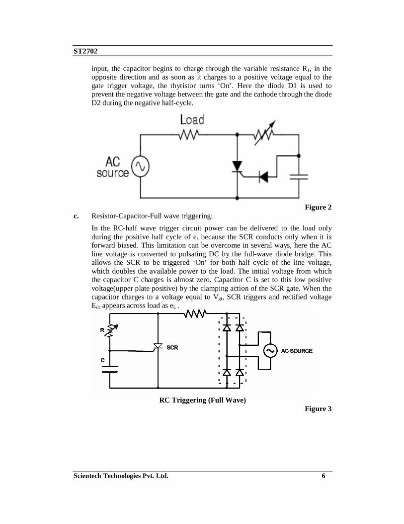
input, the capacitor begins to charge through the variable resistance R1, in the opposite direction and as soon as it charges to a positive voltage equal to the gate trigger voltage, the thyristor turns ‘On’. Here the diode D1 is used to prevent the negative voltage between the gate and the cathode through the diode D2 during the negative half-cycle.
Figure 2
c. Resistor-Capacitor-Full wave triggering: In the RC-half wave trigger circuit power can be delivered to the load only during the positive half cycle of es because the SCR conducts only when it is forward biased. This limitation can be overcome in several ways, here the AC line voltage is converted to pulsating DC by the full-wave diode bridge. This allows the SCR to be triggered ‘On’ for both half cycle of the line voltage, which doubles the available power to the load. The initial voltage from which the capacitor C charges is almost zero. Capacitor C is set to this low positive voltage(upper plate positive) by the clamping action of the SCR gate. When the capacitor charges to a voltage equal to Vgt, SCR triggers and rectified voltage Edc appears across load as eL .
RC Triggering (Full Wave)
Figure 3
ST2702
Scientech Technologies Pvt. Ltd. 7
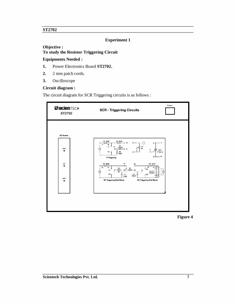
Experiment 1 Objective : To study the Resistor Triggering Circuit Equipments Needed : 1. Power Electronics Board ST2702. 2. 2 mm patch cords.
3. Oscilloscope
Circuit diagram : The circuit diagram for SCR Triggering circuits is as follows :
Figure 4

ST2702
Scientech Technologies Pvt. Ltd. 8
Procedure : 1. Connect the potentiometer points ‘D’ to point ‘d1’ and ‘E’ to point ‘e1’.
2. Connect the SCR points ‘A’ to point ‘a1’, ‘B’ to point ‘b1’ and ‘C’ to point ‘c1’. 3. Rotate the potentiometer ‘P1’ fully in clockwise direction.
4. Switch ‘On’ the power supply.
5. Connect the oscilloscope CH.I between the load test point ‘t1’ and ‘t2’ and observe the Phase angle and voltage.
6. Now, connect the oscilloscope probe across the thyristor and observe the waveform.
7. Vary the potentiometer slowly; you can see the phase angle variation.
8. Repeat the experiment from step 5 for various angles and plot the graphs.
Observation Table 1 :
S. No. Load voltage(V) Phase Angle (α)
1.
2.
3.
4.
5.
6.
ST2702
Scientech Technologies Pvt. Ltd. 9
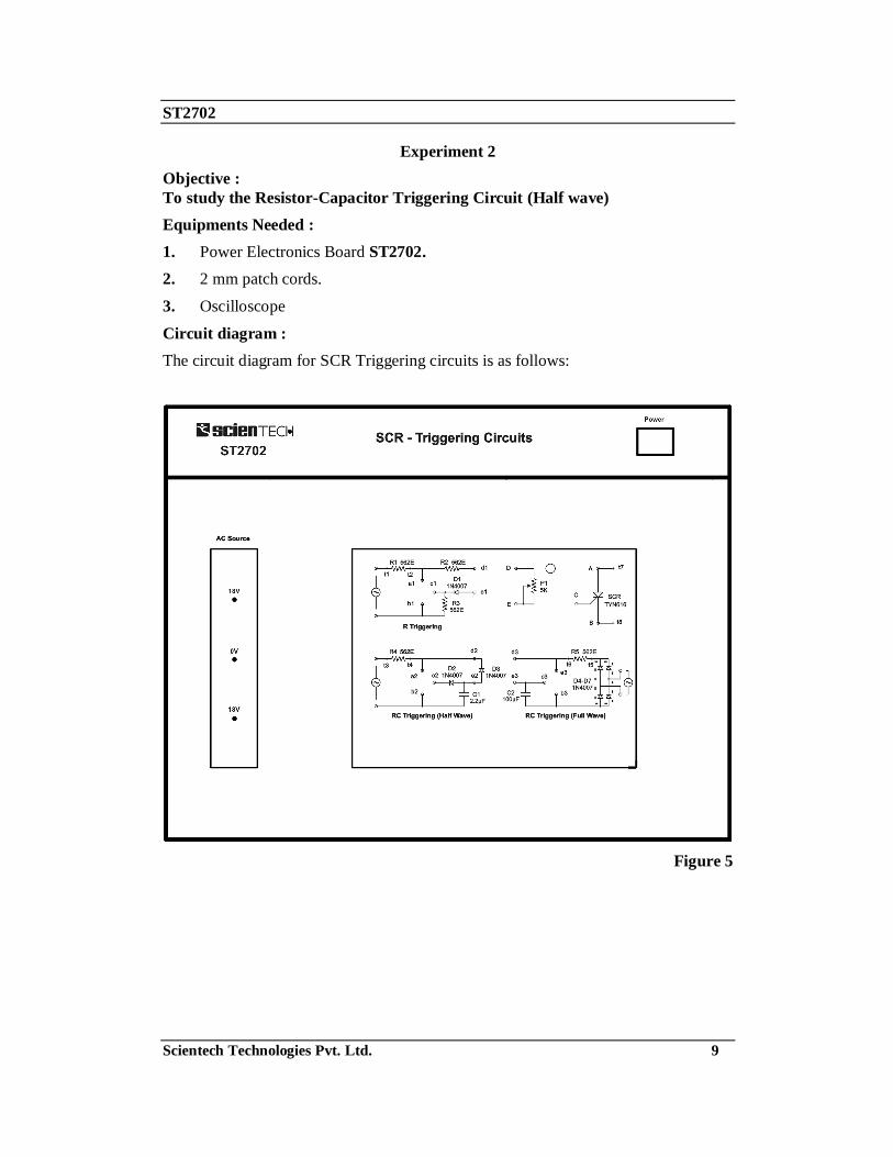
Experiment 2 Objective : To study the Resistor-Capacitor Triggering Circuit (Half wave) Equipments Needed : 1. Power Electronics Board ST2702. 2. 2 mm patch cords.
3. Oscilloscope
Circuit diagram : The circuit diagram for SCR Triggering circuits is as follows:
Figure 5

ST2702
Scientech Technologies Pvt. Ltd. 10
Procedure : 1. Connect the potentiometer points ‘D’ to point ‘d2’ and ‘E’ to point ‘e2’.
2. Connect the SCR points ‘A’ to point ‘a1’, ‘B’ to point ‘b2’ and ‘C’ to point ‘c2’. 3. Rotate the potentiometers ‘P1’ fully in the anticlockwise direction.
4. Switch ‘On’ the power supply.
5. Connect the oscilloscope probe between the load test point ‘t3’ and ‘t4’ and observe the Phase angle and voltage.
6. Now, connect the oscilloscope probe across the thyristor and observe the waveform.
7. Vary the potentiometer slowly; you can see the phase angle variation.
8. Repeat the experiment from step 5 for various angles and plot the graphs.
Observation Table 2 :
S. No. Load voltage(V) Phase Angle (α)
1.
2.
3.
4.
5.
6.

ST2702
Scientech Technologies Pvt. Ltd. 11
Experiment 3 Objective : To study the Resistor-Capacitor Triggering Circuit (Full Wave). Equipments Needed : 1. Power Electronics Board ST2702. 2. 2 mm patch cords.
3. Oscilloscope
Circuit diagram : The circuit diagram for SCR Triggering circuits is as follows:
Figure 6

ST2702
Scientech Technologies Pvt. Ltd. 12
Procedure : 1. Connect the potentiometer points ‘D’ to point ‘d3’ and ‘E’ to point ‘e3’
2. Connect the SCR points ‘A’ to point ‘a1’, ‘B’ to point ‘b3’ and ‘C’ to point ‘c3’. 3. Rotate the potentiometers ‘P1’ fully in clockwise direction.
4. Switch ‘On’ the power supply.
5. Connect the oscilloscope probe between the load test point ‘t5’ and ‘t6’ and observe the Phase angle and voltage.
6. Now, connect the oscilloscope probe across the thyristor and observe the waveform.
7. Vary the potentiometer slowly; you can see the phase angle variation.
8. Repeat the experiment from step 5 for various angles and plot the graphs.
Observation Table 3 :
S. No. Load Voltage (V) Phase Angle (α)
1.
2.
3.
4.
5.
6.

ST2702
Scientech Technologies Pvt. Ltd. 13
Datasheet
TN16 and TYNx16 Series Standard 16A SCRs
Main features
Description : The TYN / TN16 SCR Series is suitable for general purpose applications. Using clip assembly technology, they provide a superior performance in surge current capabilities.
Absolute Ratings (limiting values)

ST2702
Scientech Technologies Pvt. Ltd. 14
Warranty
1. We guarantee the product against all manufacturing defects for 24 months from the date of sale by us or through our dealers. Consumables like dry cell etc. are not covered under warranty.
2. The guarantee will become void, if
a) The product is not operated as per the instruction given in the operating manual.
b) The agreed payment terms and other conditions of sale are not followed. c) The customer resells the instrument to another party.
d) Any attempt is made to service and modify the instrument. 3. The non-working of the product is to be communicated to us immediately giving
full details of the complaints and defects noticed specifically mentioning the type, serial number of the product and date of purchase etc.
4. The repair work will be carried out, provided the product is dispatched securely packed and insured. The transportation charges shall be borne by the customer.
For any Technical Problem Please Contact us at [email protected]
List of Accessories
1. 2mm Patch Cord 16” ............................................................................ 7 Nos. 2. Mains Cord .............................................................................................1 No. 3. e-Manual.................................................................................................1 No.
Updated 22-05-2009

ST2702
Scientech Technologies Pvt. Ltd. 15
List of other Trainers available from us are : Model Name PE01 UJT Characteristics PE02 MOSFET Characteristics
PE03 SCR Characteristics
PE04 TRIAC Characteristics
PE05 DIAC Characteristics PE06 IGBT Characteristics
PE07 PUT Characteristics PE10 SCR Triggering (R, RC Full wave, RC Half wave)
PE11 SCR Triggering (UJT) PE12 SCR Triggering (IC555)
PE13 SCR Triggering (IC74121) PE14 Ramp and Pedestal Triggering
PE15 SCR Triggering (IC741) PE16 SCR Triggering (PUT)
PE40 SCR Lamp Flasher PE41 SCR Alarm Circuit
PE42 Series Inverter PE43 UJT Relaxation Oscillator
PE44 Single Phase PWM Inverter ST2701 IGBT Characteristics
ST2702 SCR Triggering (R, RC Half wave, RC Full wave) ST2703 SCR Triggering Techniques ST2704 Triggering of SCR using 74121 IC
ST2705 SCR Lamp Flasher ST2706 SCR Alarm Circuit ST2707 Series Inverter
ST2708 Single Phase Controlled Rectifier (with Ramp Comparator Firing Scheme)
ST2709 Single Phase Controlled Rectifier (Cosine Firing Scheme)

ST2702
Scientech Technologies Pvt. Ltd. 16
ST2710 Single Phase Converter Firing Techniques (by TCA 785IC and Triangular Comparator)
ST2711 Lamp Dimmer ST2712 Electronics Power Lab
ST2713 Single Phase Cyclo - Converter ST2714 Speed Control of Universal Motor using SCR
ST2715 Speed Control of AC Motor using TRIAC ST2716 Microcontroller Based Firing Circuit for Controlled Rectifier
ST2717 SCR Commutation Circuits ST2718 Bedford & Parallel Inverter ST2719 Step-Up Chopper ST2720 Single Phase Bridge Inverter
ST2722 Step-Down Chopper ST2723 AC Chopper
and many more….……