open investigation of algan/gan high electron mobility
TRANSCRIPT

1Scientific RepoRts | 6:37588 | DOI: 10.1038/srep37588
www.nature.com/scientificreports
Investigation of AlGaN/GaN high electron mobility transistor structures on 200-mm silicon (111) substrates employing different buffer layer configurationsH.-P. Lee1,2, J. Perozek1,2, L. D. Rosario1,2 & C. Bayram1,2
AlGaN/GaN high electron mobility transistor (HEMT) structures are grown on 200-mm diameter Si(111) substrates by using three different buffer layer configurations: (a) Thick-GaN/3 × {AlxGa1−xN}/AlN, (b) Thin-GaN/3 × {AlxGa1−xN}/AlN, and (c) Thin-GaN/AlN, so as to have crack-free and low-bow (<50 μm) wafer. Scanning electron microscopy, energy-dispersive X-ray spectroscopy, high resolution-cross section transmission electron microscopy, optical microscopy, atomic-force microscopy, cathodoluminescence, Raman spectroscopy, X-ray diffraction (ω/2θ scan and symmetric/asymmetric ω scan (rocking curve scan), reciprocal space mapping) and Hall effect measurements are employed to study the structural, optical, and electrical properties of these AlGaN/GaN HEMT structures. The effects of buffer layer stacks (i.e. thickness and content) on defectivity, stress, and two-dimensional electron gas (2DEG) mobility and 2DEG concentration are reported. It is shown that 2DEG characteristics are heavily affected by the employed buffer layers between AlGaN/GaN HEMT structures and Si(111) substrates. Particularly, we report that in-plane stress in the GaN layer affects the 2DEG mobility and 2DEG carrier concentration significantly. Buffer layer engineering is shown to be essential for achieving high 2DEG mobility (>1800 cm2/V∙s) and 2DEG carrier concentration (>1.0 × 1013 cm−2) on Si(111) substrates.
AlGaN/GaN high electron mobility transistors (HEMTs) are being investigated for high power high frequency applications as III-nitride (i.e. GaN) materials have high thermal and chemical stability, high breakdown field (> 3 MV/cm, 10 times of that of silicon), and high electron saturation velocity (> 2.5 × 107 cm/s, 2.5 times of that of silicon)1–3. AlGaN/GaN HEMTs are traditionally grown on sapphire (Al2O3) or silicon carbide (6H-SiC) substrates that have ~16% and ~3% lattice-mismatch with GaN, respectively4. Recently, high cost and limited diameter-scalability of these substrates fueled the research for the GaN-on-silicon (111) approach5. However, the lattice mismatch of ~17% combined with the thermal-expansion-coefficient mismatch of ~54% between GaN and Si(111) necessitate employment of novel (Al)GaN buffer layers to minimize mismatch-effects (i.e. defectivity and wafer-bow)6. It is reported that several micrometer thick buffer layers and various Al-content AlxGa1−xN layers are needed to mitigate such detrimental effects of lattice and thermal-mismatches7. Nonetheless, performance of AlGaN/GaN HEMTs is governed by the two-dimensional electron gas (2DEG) properties, which forms at the AlGaN-GaN hetero-interface and without the need of any doping – thanks to the high conduction band offset and polarization fields between AlGaN and GaN8. Particularly, a high 2DEG density reduces the source/drain contact resistance9 and increases the power output of AlGaN/GaN HEMTs3 whereas high 2DEG mobility increases the frequency performance of AlGaN/GaN HEMTs10. It is therefore imperative to study the character-istics of the 2DEG and investigate how 2DEG characteristics change under various buffer layer configurations. To do so, the same AlGaN/GaN HEMT structures need to be grown on Si(111) but with various buffer layers7.
1Department of Electrical and Computer Engineering, University of Illinois at Urbana-Champaign, Urbana, Illinois 61801, USA. 2Micro and Nanotechnology Laboratory, University of Illinois at Urbana-Champaign, Urbana, Illinois 61801, USA. Correspondence and requests for materials should be addressed to C.B. (email: [email protected])
received: 23 August 2016
Accepted: 31 October 2016
Published: 21 November 2016
OPEN
www.nature.com/scientificreports/
2Scientific RepoRts | 6:37588 | DOI: 10.1038/srep37588
Another important milestone in GaN-on-Si(111) technology is Si(111) wafer-scaling. Despite the early works on 100-mm substrates11, it is critical to scale these efforts to 200-mm substrates. This, however, is bottlenecked primarily by the large GaN-Si thermal mismatch that introduces high stress leading to significant wafer-bow12 or worse, wafer cracking13.
In this work, we grew the same AlGaN/GaN HEMT structures on 200-mm Si(111) substrates using three dif-ferent buffer layers configurations {such that all wafers are crack-free and have a small bow (< 50 μ m)} and report the effects of buffer layers on the AlGaN/GaN HEMT structures. To quantify the stress and defectivity, we inves-tigate these stacks using structural, optical and electrical characterization techniques including scanning electron microscopy (SEM), energy-dispersive X-ray spectroscopy (EDS), high resolution cross-sectional transmission electron microscopy (HR-XTEM), optical microscopy, atomic-force microscopy (AFM), cathodoluminescence (CL), Raman spectroscopy, X-ray diffraction (XRD) {ω /2θ scan, symmetric/asymmetric ω scan (rocking curve scan), and reciprocal space mapping (RSM)} and Hall effect measurements. Then we correlate the electrical prop-erties of AlGaN/GaN HEMT structures with the embodied buffer layer properties and report the effects of buffer layer stress and defectivity on the 2DEG mobility and 2DEG concentration.
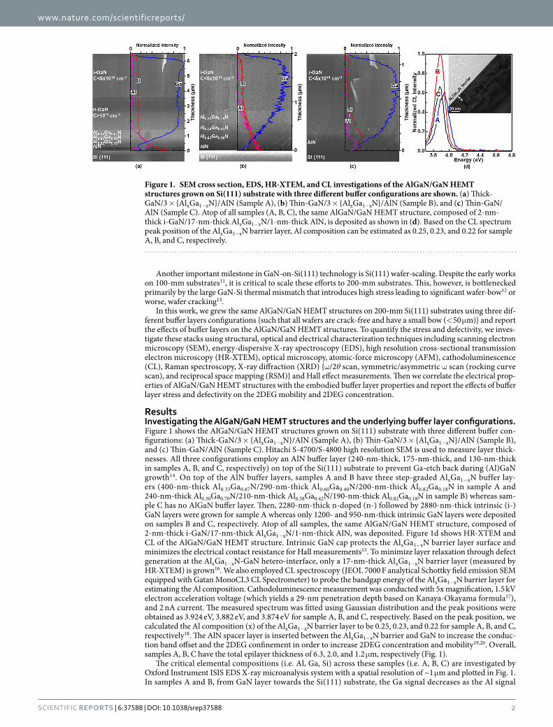
ResultsInvestigating the AlGaN/GaN HEMT structures and the underlying buffer layer configurations. Figure 1 shows the AlGaN/GaN HEMT structures grown on Si(111) substrate with three different buffer con-figurations: (a) Thick-GaN/3 × {AlxGa1−xN}/AlN (Sample A), (b) Thin-GaN/3 × {AlxGa1−xN}/AlN (Sample B), and (c) Thin-GaN/AlN (Sample C). Hitachi S-4700/S-4800 high resolution SEM is used to measure layer thick-nesses. All three configurations employ an AlN buffer layer (240-nm-thick, 175-nm-thick, and 130-nm-thick in samples A, B, and C, respectively) on top of the Si(111) substrate to prevent Ga-etch back during (Al)GaN growth14. On top of the AlN buffer layers, samples A and B have three step-graded AlxGa1−xN buffer lay-ers (400-nm-thick Al0.33Ga0.67N/290-nm-thick Al0.60Ga0.40N/200-nm-thick Al0.82Ga0.18N in sample A and 240-nm-thick Al0.30Ga0.70N/210-nm-thick Al0.58Ga0.42N/190-nm-thick Al0.82Ga0.18N in sample B) whereas sam-ple C has no AlGaN buffer layer. Then, 2280-nm-thick n-doped (n-) followed by 2880-nm-thick intrinsic (i-) GaN layers were grown for sample A whereas only 1200- and 950-nm-thick intrinsic GaN layers were deposited on samples B and C, respectively. Atop of all samples, the same AlGaN/GaN HEMT structure, composed of 2-nm-thick i-GaN/17-nm-thick AlxGa1−xN/1-nm-thick AlN, was deposited. Figure 1d shows HR-XTEM and CL of the AlGaN/GaN HEMT structure. Intrinsic GaN cap protects the AlxGa1−xN barrier layer surface and minimizes the electrical contact resistance for Hall measurements15. To minimize layer relaxation through defect generation at the AlxGa1−xN-GaN hetero-interface, only a 17-nm-thick AlxGa1−xN barrier layer (measured by HR-XTEM) is grown16. We also employed CL spectroscopy (JEOL 7000 F analytical Schottky field emission SEM equipped with Gatan MonoCL3 CL Spectrometer) to probe the bandgap energy of the AlxGa1−xN barrier layer for estimating the Al composition. Cathodoluminescence measurement was conducted with 5x magnification, 1.5 kV electron acceleration voltage (which yields a 29-nm penetration depth based on Kanaya-Okayama formula17), and 2 nA current. The measured spectrum was fitted using Gaussian distribution and the peak positions were obtained as 3.924 eV, 3.882 eV, and 3.874 eV for sample A, B, and C, respectively. Based on the peak position, we calculated the Al composition (x) of the AlxGa1−xN barrier layer to be 0.25, 0.23, and 0.22 for sample A, B, and C, respectively18. The AlN spacer layer is inserted between the AlxGa1−xN barrier and GaN to increase the conduc-tion band offset and the 2DEG confinement in order to increase 2DEG concentration and mobility19,20. Overall, samples A, B, C have the total epilayer thickness of 6.3, 2.0, and 1.2 μ m, respectively (Fig. 1).
The critical elemental compositions (i.e. Al, Ga, Si) across these samples (i.e. A, B, C) are investigated by Oxford Instrument ISIS EDS X-ray microanalysis system with a spatial resolution of ~1 μ m and plotted in Fig. 1. In samples A and B, from GaN layer towards the Si(111) substrate, the Ga signal decreases as the Al signal
Figure 1. SEM cross section, EDS, HR-XTEM, and CL investigations of the AlGaN/GaN HEMT structures grown on Si(111) substrate with three different buffer configurations are shown. (a) Thick-GaN/3 × {AlxGa1−xN}/AlN (Sample A), (b) Thin-GaN/3 × {AlxGa1−xN}/AlN (Sample B), and (c) Thin-GaN/AlN (Sample C). Atop of all samples (A, B, C), the same AlGaN/GaN HEMT structure, composed of 2-nm-thick i-GaN/17-nm-thick AlxGa1−xN/1-nm-thick AlN, is deposited as shown in (d). Based on the CL spectrum peak position of the AlxGa1−xN barrier layer, Al composition can be estimated as 0.25, 0.23, and 0.22 for sample A, B, and C, respectively.

www.nature.com/scientificreports/
3Scientific RepoRts | 6:37588 | DOI: 10.1038/srep37588
increases, as we have step-graded AlxGa1−xN layers. In sample C a rather rounded Al signal peak is observed as it has no step-graded AlxGa1−xN layers. The Si signal increases in all samples towards the substrate showing the Si diffusion.
Surface investigation of the AlGaN/GaN HEMT structures via optical microscope, atomic force microscopy, and cathodoluminescence. Figure 2 shows the surface studies of all samples (A, B, C) by optical microscopy (Fig. 2a,b,c), atomic force microscopy (Fig. 2d,e,f) and CL (Fig. 2g,h,i). No surface cracks are observed in any samples, indicating high film quality13. Atomic force microscopy (Asylum Cypher S AFM with tapping mode) is used to study the surface roughness and contour of the AlGaN/GaN HEMT structures. Figure 2d,e,f show 5 μ m × 5 μ m AFM scans. It is important to note that the average root-mean-square (RMS) roughnesses are similar across samples (5.5 ± 2.8, 5.2 ± 1.4, and 5.1 ± 1.3 Å, for A, B, and C, respectively), wherein sample A has the largest surface roughness. In order to quantify surface-terminated defects (i.e. dislocations with threading component), we counted the “dark spots” on the AFM images (Fig. 2d,e,f)21 which averaged as 1.8 ± 0.3 × 10⁹, 2.2 ± 0.8 × 10⁹, and 2.6 ± 0.8 × 109 cm−2 (Table 1) for samples A, B, and C, respectively, showing thickest sample (A) having the lowest density of threading type dislocations, in agreement with other works22,23. Based on their different sizes these dark spots can be classified as pure-edge type (small), pure-screw type (large) and mixed-type (middle) threading dislocations.
Cathodoluminescence is also a useful tool in highlighting the surface defects as defects are centers of non-radiative recombination and appear dark in a panchromatic view24. We again employed the same CL
Figure 2. Optical microscopy, AFM and CL images of samples A, B and C are shown. Optical microscopy (a,b,c) reveals no surface cracks. AFM (d,e,f) reveals the average root-mean-square (RMS) roughness of 5.5 ± 2.8, 5.2 ± 1.4, and 5.1 ± 1.3 Å for sample A, B, and C, respectively, suggesting a similar surface profile. Cathodoluminescence (g,h,i) reveals defectivity of sample A, B, and C as 1.0 ± 0.3 × 10⁹, 2.0 ± 0.3 × 10⁹, 1.8 ± 0.3 × 109 cm−2, respectively. AFM and CL studies agree that sample A (the thickest sample) has the lowest threading dislocation defect density whereas sample C (the thinnest sample) has the highest one (Table 1).

www.nature.com/scientificreports/
4Scientific RepoRts | 6:37588 | DOI: 10.1038/srep37588
spectroscopy system to study these samples. A panchromatic CL image using a 2.0-kV electron acceleration volt-age (that gives a penetration depth of 47 nm17) reveals the defect distribution as shown in Fig. 2g,h,i. The average CL defectivity for samples A, B, and C are measured as 1.0 ± 0.3 × 10⁹, 2.0 ± 0.3 × 10⁹, and 1.8 ± 0.3 × 109 cm−2 (Table 1), respectively. This suggests, similar to our AFM results, that the thickest sample A has the least defectiv-ity. With respect to AFM analysis, CL underestimates the defectivity because defects have capture radius, suggest-ing that multiple defects are located within one CL dark capture radius.
Layer stress analysis through Raman measurements, X-ray diffraction and reciprocal space mapping. We studied the GaN stress via Horiba Raman Confocal Imaging Microscope using 633-nm laser line (with a grating of 1800 lines/mm, yielding a resolution of 1.19 cm−1). A 2″ Si(111) wafer was first utilized for spectrum verification and a 521.9 cm−1 peak was obtained, as shown in Figure S1. Under Z(XX)Z configuration, E2
H and A1(LO) Raman peaks are measured, and the shifts in these Raman peaks from the stress-free values of 567.5 cm−1 (E2
H) at 300 K are recorded. Based on the shift direction and the shift amount (∆ ω ) of E2H, we deter-
mined the stress type as compressive and calculated the stress amount (σxx) through11
σ ω=∆.
⋅4 3
cm GPa (1)xx
and tabulated them in Table 1. The Raman spectra of sample A, B, and C are also plotted in Fig. 3. Our Raman spectroscopy investigation suggests that sample B is under the largest compressive stress (0.488 GPa) whereas sample C is under the smallest compressive stress (0.047 GPa) and sample A has the medium value (0.256 GPa). These results are similar to other Raman works on AlGaN/GaN HEMT structures on Si(111)11.
We further quantify the (Al)GaN layers’ composition, strain, and defect density via XRD25,26. Here we employ PANalytical/Philips X’pert MRD system with 0.154-nm-wavelength radiation to study all samples. Omega/2Theta (ω /2θ) scan is used to probe the symmetrical lattice plane (0002) to determine the Al compositions of the AlxGa1−xN buffer layers according to:
= − −−
x c c c c( )/( ), (2)Al Al Ga N GaN AlN GaNxx 1
where c represents the lattice constant along the c axis calculated via Vegard’s law27. Figure 4 shows the ω /2θ scans of samples A, B, and C. The narrowest FWHM of sample B indicates the highest crystalline order amongst the samples, whereas sample A has the lowest crystalline order indicated by its widest FWHM. However, one should be aware that the Al composition results obtained from XRD ω /2θ scan can be inaccurate since both the epilayer
Sample (Epi thickness)
AFM surface
roughness (Å)
Defectivity (109 cm−2) GaN stress (GPa) Electrical property
AFM CL
XRD XRD Raman Rs (Ω/◽) 2DEG Ns (1013 cm−2) 2DEG μn (cm2/V-s)
Dscrew Dedge Tensile Compressive RT 77 K RT 77 K RT 77 K
A (6.3 μ m) 5.5 ± 2.8 1.8 ± 0.3 1.0 ± 0.3 0.40 1.02 1.059 0.256 431.8 ± 109.8 110.8 ± 28.1 1.20 ± 0.01 1.30 ± 0.10 1295 ± 247 4867 ± 996
B (2.0 μ m) 5.2 ± 1.4 2.2 ± 0.8 2.0 ± 0.3 0.58 1.47 0.154 0.488 385.8 ± 28.1 66.5 ± 5.0 0.89 ± 0.01 1.00 ± 0.01 1802 ± 102 9175 ± 698
C (1.1 μ m) 5.1 ± 1.3 2.6 ± 0.8 1.8 ± 0.3 0.39 1.02 1.548 0.047 445.5 ± 75.3 96.0 ± 23.0 0.92 ± 0.05 1.00 ± 0.10 1593 ± 268 6930 ± 1541
Table 1. Structural (surface roughness, defectivity, stress) and electrical (contact resistance, 2DEG concentration, 2DEG mobility) properties of samples A, B, and C are tabulated.
Figure 3. Raman spectroscopy of all samples A, B, and C are shown.

www.nature.com/scientificreports/
5Scientific RepoRts | 6:37588 | DOI: 10.1038/srep37588
strain and alloy composition will significantly affect the peak position of the ω /2θ scan; to estimate the Al compo-sition more precisely, XRD reciprocal space mapping is necessary.
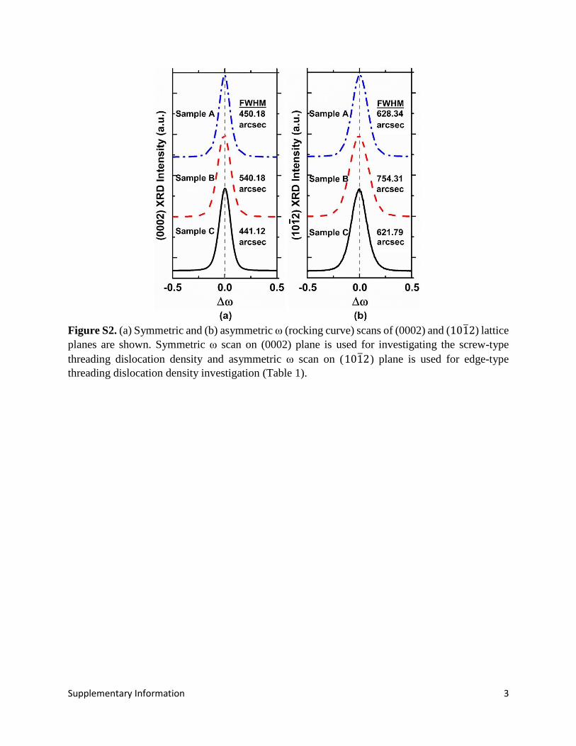
In addition, we conducted (0002) (symmetric) and (1012) (asymmetric) ω scans to estimate the densities of screw-type (Burgers vector length: 0.5185 nm (bscrew)) and edge-type (Burgers vector length: 0.3189 nm (bedge)) threading dislocations, respectively (Figure S2)25,28,29. Based on the FWHM of (0002) (symmetric) and (1012) (asymmetric) ω scans (i.e. β(0002) and β(1012)), screw- and edge-type threading dislocation densities (Dscrew and Dedge) are estimated via25,28,29:
β=.
Db4 35
,(3)
screw(0002)2
screw2
β β=
−
.D
b4 35 (4)edge
(1012)2
(0002)2
edge2
and tabulated in Table 1. Our XRD analysis suggests that sample A and C have similar amount of pure-edge- and screw-type threading dislocation densities.
X-ray diffraction reciprocal space mappings of (0002) and (1015) planes (Fig. 5) are performed to quantify the (Al)GaN layers’ strain and stress; in addition, the Al composition can be more precisely quantified compared to the ω /2θ scan. Lattice constants a and c of each layer (GaN, AlxGa1−xN, AlN) are obtained from Fig. 5 via the equation:
=
+ +
+
dh hk k
alc
1 43
,(5)hkl
2 2 2
2
2
2
where dhkl represents the interplanar spacing of the probed lattice plane (hkl)30. Employing the Poisson-Vegard’s law30 while including the lattice constant bowing parameter31, the Al composition (x), the free-standing lattice constants (a0(x) and c0(x)), and the in-plane (εxx) and out-of-plane strain (εzz) of each layer are calculated via:
δδ
−= −
−×
−
= + − + ⋅ ⋅ −= + − + ⋅ ⋅ −
= + −
c x c xc x
v xv x
a x a xa x
c x xc x c x xa x xa x a x x
v x xv x v
( ) ( )( )
2 ( )1 ( )
( ) ( )( )
( ) (1 ) (1 )( ) (1 ) (1 )
( ) (1 ) , (6)
m m0
0
0
0
0 AlN GaN c
0 AlN GaN a
0 AlN GaN
ε = −a x a x a x[ ( ) ( )]/ ( ), (7)xx m 0 0
ε = −c x c x c x[ ( ) ( )]/ ( ) (8)zz m 0 0
am(x) and cm(x) are the measured lattice constants obtained from Eq. 5; aAlN = 3.112 Å, cAlN = 4.982 Å, aGaN = 3.186 Å, and cAlN = 5.186 Å, representing free-standing lattice constants. The Poisson ratio vAlN and vGaN are 0.203 and 0.183, respectively30. δc and δa represent the deviation (bowing) parameter and were fit to be − 0.036 and 0.018 Å, respectively31. The in-plane stress (σ )xx is also calculated according to:
σ ε= + − ×C C C C[( ) 2 / ] , (9)xx xx11 12 132
33
where Cij are the elastic constants of GaN (C11 = 390 GPa, C12 = 145 GPa, C13 = 106 GPa, and C33 = 398 GPa)32. The resulting in-plane stress values of GaN layers are tabulated in Table 1. Detailed XRD RSM calculation results,
Figure 4. Symmetric XRD ω/2θ scans of samples A, B, and C are used to determine the Al-content and crystalline quality. Results show sample B having the narrowest FWHM values – suggesting the best crystallography quality amongst all samples.

www.nature.com/scientificreports/
6Scientific RepoRts | 6:37588 | DOI: 10.1038/srep37588
including the lattice constants (a and c), in-plane strain/stress, and out-of-plane strain of each (Al)GaN layer in all samples, are provided in Supplementary Table SI. The in-plane strain of each (Al)GaN layer of the three samples are also plotted in Supplementary Figure S3. For sample A and B, from the AlN layer toward the AlxGa1−xN layers the in-plane strain first decreases from positive (tensile), crossing the zero line (strain-free), and then become negative (compressive). Finally the in-plane strain returns to positive (tensile) due to the growing of the GaN layer. This discovered trend agrees with a previous work33 where the in-plane strain in a GaN/AlxGa1−xN/AlN system initially decreases along the increasing of the structure thickness and then crosses the zero line; as the thickness of GaN gets thicker the slope gets less steep, suggesting that an in-plane strain with a tensile component launches and becomes more dominant as the GaN thickness gets thicker.
Our XRD RSM results suggest that the GaN layers of all the three samples have tensile stress with sample B having the lowest stress (~0.154 GPa), sample C having the highest one (~1.548 GPa), and sample A having a medium value (~1.059 GPa). This indicates that the step-graded AlxGa1−xN layers used in samples A and B reduce
Figure 5. XRD reciprocal space mapping results reveal that the GaN layers of all samples (A, B, C) are under tensile strain along the c-plane and are under compressive strain normal to the c-plane. Amongst, sample B is observed to have the lowest GaN in-plane stress (Table 1).

www.nature.com/scientificreports/
7Scientific RepoRts | 6:37588 | DOI: 10.1038/srep37588
the in-plane (tensile) stress of the GaN layer. Moreover, GaN in sample A is shown to have a higher in-plane ten-sile stress than GaN in sample B. We attribute this to sample A having a thicker GaN layer (a thicker i-GaN layer and an additional n-GaN layer) than sample B. Moreover, it’s been reported that smaller-sized dopants, such as Si, in GaN films will from impurity atmospheres that limit the dislocation movement while growing, which further limits the dislocation reduction and the relief of the GaN tensile stress34. At this stage, we fairly believe that the carbon dopant in the n-doped GaN in sample A has an equivalent effect on enlarging the GaN film tensile stress. This indicates the importance of optimal buffer layer configuration in terms of thicknesses and Al-content.
Investigation of the two dimensional electron gas characteristics via Hall effect measurement. Hall effect measurements under Van der Pauw configuration are carried out at room (300 K) and low (77 K) temperatures. The metal contacts are formed via e-beam evaporation of 200-nm-thick Ti/200- nm-thick Ni metal stack and annealed at 750 °C under N2 for 45 seconds. Samples are then diced into 5 mm × 5 mm squares and measured under Van der Pauw configuration.
Carrier concentration (Ns), sheet resistance (Rs), and mobility (μ n) of samples A, B, and C are tabulated in Table 1. The 2DEG concentration is the highest in sample A, whereas 2DEG mobility is highest in sample B. It is earlier reported that carrier concentration and mobility of a 2DEG system are strongly related35. At high 2DEG carrier concentration (> ~ 2 × 1012 cm−3), the 2DEG mobility has a negative dependence on increasing carrier concentration due to the surface roughness scattering, in agreement with our work. At low temperature (77 K), the 2DEG mobility increases and the sheet resistance decreases in all samples due to the reduced phonon scatter-ing at low (77 K) temperature. Furthermore, 2DEG concentrations in all our samples are higher at 77 K than at 300 K, in line with other works36.
DiscussionOur defectivity measurements via AFM and CL reveal that threading dislocation density reduces with increasing total buffer thickness. We further show step-graded AlGaN buffer layers and thicker GaN buffer layers alone are beneficial in doing so. This is attributed to the interaction of edge- and mixed-type threading dislocations in the forms of fusion (i.e. two threading dislocation lines merging into one) and annihilation (two threading disloca-tion lines (having opposite Burgers vectors) annihilating one another)14. As the (Al)GaN film is further deposited, the possibility of such interactions increases, lowering the threading dislocation density. In particular, the inaccu-racy of CL and XRD defectivity measurements are discussed here. As mentioned, CL measurement tend to under-estimate the defectivity because these defects act as non-radiative recombination centers that possess capture radius; compared to AFM defectivity the lower defectivity of CL suggests that multiple defects are located within one CL dark capture radius. On the other hand, the estimated XRD defectivity here provides information about the densities of the pure-screw- and pure-edge-type threading dislocations; mixed-type threading dislocation, which typically occupies a large portion of the total defectivity, is not evaluated. In addition, although we conduct asymmetric rocking curve scan on the commonly used (1012) plane to estimate the pure-edge-type threading dislocations, the measured XRD rocking curve FWHM is not solely affected by threading dislocations; other factors such as instrumental broadening, microstrain, and wafer curvature also play roles in changing the FWHM25. We suggest to take the AFM defectivity as the total defectivity as it is the most direct and sensitive one, which concludes that sample C should possess a large amount of mixed-type threading dislocations that achieves its largest total defectivity.
X-ray diffraction RSM is used to investigate strain distribution in buffer layers (Fig. 5) providing in-/out-of-plane strain information of GaN, AlxGa1−xN, and AlN layers (Table S1). In samples A, B and C, the AlN in-plane tensile strain are found to be 0.47%, 0.51%, and 0.52%, respectively. We observe a gradual reduction of in-/out-of-plane tensile strain in the step-graded 3 × {AlxGa1−xN} buffer layers from Si(111) towards the AlGaN/GaN HEMT structure (Table S1 and Figure S3). This leads to a lower tensile GaN in-plane strain in samples A (0.23%) and B (0.03%) than that in sample C (0.34%), showing the importance of step-graded AlxGa1−xN buffer layers. Between sample A and B, GaN in-plane tensile strain in sample B is lower than that in sample A leading to a narrower XRD FWHM (Fig. 4). Although Raman spectroscopy reveals a blue shift of GaN E2
H Raman peak in all samples, which corresponds to an in-plane compressive stress (< 0.5 GPa), in line with other Raman works11. The discrepancy between the stress results from XRD RSM and Raman spectroscopy has been found in previous works37,38, which is suggested to be attributed to the fact that the stress measured by XRD RSM is an average value throughout the whole structure where the effect brought by local/random lattice distortion and/or any other imperfections are averaged out. On the other hand, the stress investigated by Raman spectroscopy is only from the spot-size area, therefore the value is statistically insufficient and less accurate to represent the strain in the whole GaN layer. In addition, it is reported that the discrepancy will also occur when the material is doped and/or with impurities37. Furthermore, stress investigation using Raman Spectroscopy requires a phonon-shift esti-mation model, which might need to be modified for short period hetero-interfaces such as AlGaN/GaN HEMTs. Thus, we believe XRD RSM to be a more reliable means of probing the stress in thick hetero-interfaced layers than Raman studies.
Hall effect measurements under Van der Pauw configuration are carried out to determine 2DEG concentra-tion, sheet resistance, and 2DEG mobility (Table 1). Sheet resistance is inversely related to the 2DEG mobility, however the relatively large variation of the sheet resistance of sample A and C should be attributed to the surface variation across the samples as the surface morphology is significantly affected by defects. As the defect density and type is varied, it is typical to have a varying surface morphology, and such variation in surface morphology greatly affects the contacts as defects are charged as well as some defects have threading component (during annealing metal is diffused further). The 2DEG concentration is the highest in sample A and the lowest in sample B whereas the 2DEG mobility is the highest in sample B and the lowest in sample A, showing a trade-off between 2DEG concentration and 2DEG mobility35. Considering that sample A has the lowest threading dislocations but
www.nature.com/scientificreports/
8Scientific RepoRts | 6:37588 | DOI: 10.1038/srep37588
sample B has the lowest in-plane strain, our work suggests that 2DEG mobility is not only affected by threading dislocations but also by GaN in-plane strain. As 2DEG concentration is affected by the spontaneous (PSP) and pie-zoelectric (PPE) polarizations in the AlxGa1−xN barrier layer and the underlying GaN layer (where the piezoelectric polarization is determined by strain8), a fixed polarization charge density (C/m2) is induced at the AlGaN/GaN hetero-interface given by:
σ + = −= −+ −
−
−
−
P P P PP PP P
( ) (GaN) (Al Ga N){ (GaN) (Al Ga N)}{ (GaN) (Al Ga N)}, (10)
x x
x x
x x
SP PE 1
PE PE 1
SP SP 1
where PSP doesn’t change with strain whereas PPE follows:
=−
−
.P a a
ae e C
C2
(11)PE
0
031 33
13
33
where (C13, C33) are elastic constants and (e31, e33) are piezoelectric coefficients. For PPE (GaN), a0 = 3.186 Å, e31 = − 0.49 C/m2, e33 = 0.73 C/m2, C13 = 103 GPa, and C33 = 405 GPa; for PPE(AlxGa1−xN, x = 0.25, 0.23, and 0.22 in sample A, B, and C, respectively), a0 ≅ 3.165 Å, e31 ≅ − 0.52 C/m2, e33 ≅ 0.92 C/m2, C13 ≅ 104.25 GPa, and C33 ≅ 397 GPa8. Since the AlxGa1−xN barrier layer is thin (~17 nm), we fairly assume that it is fully strained with no relaxation, which allows us to further assume that the lattice constant a of the AlxGa1−xN barrier layer should be the same with that of the GaN layer. From Eqn. 11, we obtain: PPE(GaN)–PPE(AlxGa1−xN) ≅ 0.057a–0.172, suggesting that as lattice constant a becomes larger (meaning that both the AlxGa1−xN barrier and GaN layers simultaneously stretch further under more tensile strain), {PPE(GaN)–PPE(AlxGa1−xN)} value and hence the polar-ization charge density (σ) increase. The increase in the polarization charge density results in an increase in 2DEG concentration, in good agreement with our observations. As stated before, the higher 2DEG concentration of sample A and C (due to their larger GaN tensile stress) is responsible for their lower 2DEG mobility because of the severer surface roughness scattering. In summary, we report that GaN layer in-plane tensile strain is the dominant mechanism governing the 2DEG characteristics.
ConclusionScanning electron microscopy, energy-dispersive X-ray spectroscopy, high resolution-cross section transmission electron microscopy, optical microscopy, atomic-force microscopy, cathodoluminescence, Raman spectroscopy, X-ray diffraction (ω /2θ scan, symmetric/asymmetric ω scan (rocking curve scan), and reciprocal space mapping), and Hall effect measurements are utilized to investigate AlGaN/GaN HEMT structures on Si(111) with different buffer layer configurations. We show that thicker buffer layers are beneficial for reducing the threading disloca-tion density, and stacked AlxGa1−xN buffer layers are critical for reducing the layer stress. Furthermore, our work suggests that the type and the magnitude of in-plane strain of the GaN layer, not the threading dislocation density, dominate the 2DEG mobility. Overall, we demonstrate the importance of optimal buffer layer configurations for 2DEG characteristics, which might allow high-frequency AlGaN/GaN HEMT designs on Si(111) substrates.
MethodsSample preparation and cleaning. The AlGaN/GaN heterostructures used for this investigation are cut from three different 200-mm-diameter wafers (A, B, and C) with Si(111) substrate. The epitaxy layer configura-tions are shown in Fig. 1. Samples (8 pieces of sample A from the wafer A, 18 pieces of sample B from the wafer B, and 6 pieces of sample C from the wafer C) populate on the wafer approximately ~15 cm away from the center. Sample cleaning is carried out as follows: Samples are soaked in (1) hot trichloroethylene (TCE), (2) hot acetone, (3) hot methanol followed by (4) DI rinse and (5) N2 blow dry. For steps (1–3), an ultrasonic bath cleaning is added. All steps are carried out for ~10 minutes.
Metallization, annealing, and dicing of AlGaN/GaN HEMT structures for Hall measurements. After sample cleaning, 200-nm titanium (Ti) and then 200-nm nickel (Ni) metal contacts were deposited through a square-shaped patterned hard mask on the Hall mobility measurement samples. The metal deposition rates were kept between 1.5 and 2.0 Å/s. Rapid thermal annealing was carried out at 750 °C for 45 s under N2 for ohmic con-tact formation. Then, photoresist (PR) (AZ 5214) was spun on the samples then soft-baked at 95 °C for ~10 min in order to prevent scratching or damaging the sample surface during dicing. Finally, nickel-bond dicing blade (0.051 mm thick, 3–6 micron diamond grain size) mounted on K&S 708 dicing saw is used for dicing samples into small square dies with metal contacts in the four corners. Samples were re-cleaned before measurements. Hall measurement were performed three times for each piece of sample. Finally we calculate the overall averages and standard deviations of the measured data from these three kinds of samples.
References1. Pengelly, R. S., Wood, S. M., Milligan, J. W., Sheppard, S. T. & Pribble, W. L. A Review of GaN on SiC High Electron-Mobility Power
Transistors and MMICs. IEEE Trans. Microw. Theory Tech. 60, 1764 (2012).2. Ishida, M., Ueda, T., Tanaka, T. & Ueda, D. GaN on Si Technologies for Power Switching Devices. IEEE Trans. Electron Dev. 60, 3053
(2013).3. Baliga, B. J. Gallium nitride devices for power electronic applications. Semicond. Sci. Technol. 28, 074011 (2013).4. Kukushkin, S. A. et al. Substrate for epitaxy of gallium nitride: new material and techniques. Rev. Adv. Mater. Sci. 17, 1 (2008).5. Dadgar, A. et al. Metalorganic Chemical Vapor Phase Epitaxy of Crack-Free GaN on Si(111) Exceeding 1 μ m in Thickness. Jpn. J.
Appl. Phys. 39, L 1183 (2000).6. Krost, A. & Dadgar, A. GaN-Based Devices on Si. Phys. Stat. Sol. (a) 194, 361 (2002).

www.nature.com/scientificreports/
9Scientific RepoRts | 6:37588 | DOI: 10.1038/srep37588
7. Able, A., Wegscheider, W., Engl, K. & Zweck, J. Growth of crack-free GaN on Si(111) with graded AlGaN buffer layers. J. Cryst. Growth. 276, 415 (2005).
8. Ambacher, O. et al. Two dimensional electron gases induced by spontaneous and piezoelectric polarization in undoped and doped AlGaN/GaN heterostructures. J. Appl. Phys. 87, 334 (2000).
9. Saito, W. et al. High Breakdown Voltage AlGaN–GaN Power-HEMT Design and High Current Density Switching Behavior. IEEE Trans. Electron Dev. 50, 2528 (2003).
10. Trew, R. J. High-frequency solid-state electronic devices. IEEE Trans. Electron Dev. 52, 638 (2005).11. Cheng, J. et al. Growth of high quality and uniformity AlGaN/GaN heterostructures on Si substrates using a single AlGaN layer with
low Al composition. Sci. Rep. 6, 23020 (2016).12. Miyoshi, M., Watanabe, A. & Egawa T. Modeling of the wafer bow in GaN-on-Si epiwafers employing GaN/AlN multilayer buffer
structure. Semicond. Sci. Technol. 31, 105016 (2016).13. Arslan, E. et al. Buffer optimization for crack-free GaN epitaxial layers grown on Si(111) substrate by MOCVD. J. Phys. D: Appl.
Phys. 41, 155317 (2008).14. Zhu, D., Wallis, D. J. & Humphreys, C. J. Prospects of III-nitride optoelectronics grown on Si. Rep. Prog. Phys. 76, 106501 (2013).15. Makaram, P., Joh, J., del Alamo, Jesús A., Palacios, T. & Thompson, C. V. Evolution of structural defects associated with electrical
degradation in AlGaN/GaN high electron mobility transistors. Appl. Phys. Lett. 96, 233509 (2010).16. Lee, S. R. et al. In situ measurements of the critical thickness for strain relaxation in AlGaN/GaN heterostructures. Appl. Phys. Lett.
85, 6164 (2004).17. Kanaya, K. & Okayama, S. Penetration and energy-loss theory of electrons in solid targets. J. Phys. D.: Appl. Phys. 5, 43 (1972).18. Takahashi, K., Yoshikawa, A. & Sandhu, A. Wide Bandgap Semiconductors - Fundamental Properties and Modern Photonic and
Electronic Devices (Springer-Verlag, Berlin Heidelberg, 2007).19. Nanjo, T. et al. Enhancement of Drain Current by an AlN Spacer Layer Insertion in AlGaN/GaN High-Electron-Mobility Transistors
with Si-Ion-Implanted Source/Drain Contacts. Jpn. J. Appl. Phys. 50, 064101 (2011).20. Wosko, M., Paszkiewicz, B., Paszkiewicz, R. & Tlaczala, M. Influence of AlN spacer on the properties of AlGaN/AlN/GaN
heterostructures. Opt. Appl. 43, 61 (2013).21. Bayram, C., Pau, J. L., McClintock, R. & Razeghi, M. Comprehensive study of blue and green multi-quantum-well light-emitting
diodes grown on conventional and lateral epitaxial overgrowth GaN. Appl Phys B 95, 307 (2009).22. Mathis, S. K. et al. Modeling of threading dislocation reduction in growing GaN layers. J. Cryst. Growth. 231, 371 (2001).23. Speck, J. S., Brewer, M. A., Beltz, G., Romanov, A. E. & Pompe, W. Scaling laws for the reduction of threading dislocation densities
in homogeneous buffer layers. J. Appl. Phys. 80, 3808 (1996).24. Rosner, S. J., Carr, E. C., Ludowise, M. J., Girolami, G. & Erikson, H. I. Correlation of cathodoluminescence inhomogeneity with
microstructural defects in epitaxial GaN grown by metalorganic chemical-vapor deposition. Appl. Phys. Lett. 70, 420 (1997).25. Moram, M. A. & Vickers, M. E. X-ray diffraction of III-nitrides. Rep. Prog. Phys. 72, 036502 (2009).26. Sardela, M. R. Jr. Practical Materials Characterization 10–12 (Springer, New York, 2014).27. Denton, A. R. & Ashcroft, N. W. Vegard’s law. Phys. Rev. A 43, 3161 (1991).28. Shan, L. et al. Super-aligned carbon nanotubes patterned sapphire substrate to improve quantum efficiency of InGaN/GaN light-
emitting diodes. Optics Express 23, A957 (2015).29. Wong, Y.-Y. et al. The effect of AlN buffer growth parameters on the defect structure of GaN grown on sapphire by plasma-assisted
molecular beam epitaxy. J. Cryst. Growth. 311, 1487 (2009).30. Kadir, A., Huang, C.-C., Lee, K. E.-K., Fitzgerald, E. A. & Chua, S.-J. Determination of alloy composition and strain in multiple
AlGaN buffer layers in GaN/Si system. Appl. Phys. Lett. 105, 232113 (2014).31. Liou, B.-T., Yen, S.-H. & Kuo, Y.-K., Vegard’s law deviation in band gaps and bowing parameters of the wurtzite III-nitride ternary
alloys. Proc. SPIE 5628, Semiconductor Lasers and Applications II, (20 January 2005).32. Kuball, M. Raman spectroscopy of GaN, AlGaN and AlN for process and growth monitoring/control. Surf. Interface Anal. 31, 987
(2001).33. Mohan, N., Manikant, Soman, R. & Raghavan, S. Integrating AlGaN/GaN high electron mobility transistor with Si: A comparative
study of integration schemes. J. Appl. Phys. 118, 135302 (2015).34. Moram, M. A. et al. The effects of Si doping on dislocation movement and tensile stress in GaN films J. Appl. Phys. 109, 073509
(2011).35. Katz, O., Horn, A., Bahir, G. & Salzman. J. Electron Mobility in an AlGaN/GaN Two-Dimensional Electron Gas I—Carrier
Concentration Dependent Mobility. IEEE Trans. Electron Dev. 50, 2002 (2003).36. Acar S., Lisesivdin S. B., Kasap M., Özçelik S. & Özbay E., Determination of two-dimensional electron and hole gas carriers in
AlGaN/GaN/AlN heterostructures grown by Metal Organic Chemical Vapor Deposition. Thin Solid Films 516, 2041 (2008).37. Ferreira, N. G., Abramof, E., Corat, E. J. & Trava-Airoldi, V. J. Residual stresses and crystalline quality of heavily boron-doped
diamond films analyzed by micro-Raman spectroscopy and X-ray diffraction. Carbon 41, 1301 (2003).38. Liu, J. et al. Unintentionally doped high resistivity GaN layers with an InGaN interlayer grown by MOCVD. RSC Adv. 6, 60068
(2016).
AcknowledgementsThis work was partially supported by the Air Force Office of Scientific Research (AFOSR) through Young Investigator Program Grant FA9550-16-1-0224 and was carried out in the Micro and Nanotechnology Laboratory and Frederick Seitz Materials Research Laboratory Central Facilities, University of Illinois at Urbana-Champaign, IL, USA. The authors acknowledge support from Dr. Mauro Sardela and Dr. James Mabon from Frederick Seitz Materials Research Laboratory. L. D. Rosario acknowledges financial support by the National Science Foundation under grant #NSF EEC-1359454 REU, as part of the nano@illinois project, managed and coordinated through the Center for Nanoscale Science and Technology collaboratory and the Micro and Nanotechnology Lab at the University of Illinois at Urbana-Champaign, IL, USA.
Author ContributionsC.B. conceived the idea and performed the epitaxial growth. H.-P.L. and C.B. designed the experiments. H.-P.L., J.P. and L.D. R performed fabrication/characterization of all samples. H.-P.L. and C.B. wrote the manuscript. H.-P.L. performed optical microscopy, SEM, EDX, AFM, XRD and Raman measurements. H.-P.L., J.P., and L.D.R carried out Hall measurements. H.-P.L. and C.B. participated in data analysis. All authors discussed the results and commented on the manuscript.
Additional InformationSupplementary information accompanies this paper at http://www.nature.com/srep

www.nature.com/scientificreports/
1 0Scientific RepoRts | 6:37588 | DOI: 10.1038/srep37588
Competing financial interests: The authors declare no competing financial interests.How to cite this article: Lee, H.-P. et al. Investigation of AlGaN/GaN high electron mobility transistor structures on 200-mm silicon (111) substrates employing different buffer layer configurations. Sci. Rep. 6, 37588; doi: 10.1038/srep37588 (2016).Publisher's note: Springer Nature remains neutral with regard to jurisdictional claims in published maps and institutional affiliations.
This work is licensed under a Creative Commons Attribution 4.0 International License. The images or other third party material in this article are included in the article’s Creative Commons license,
unless indicated otherwise in the credit line; if the material is not included under the Creative Commons license, users will need to obtain permission from the license holder to reproduce the material. To view a copy of this license, visit http://creativecommons.org/licenses/by/4.0/ © The Author(s) 2016

Supplementary Information 1
Supplementary Online Material for: “Investigation of AlGaN/GaN high electron mobility
transistor structures on 200-mm silicon (111) substrates employing different buffer layer
configurations”
H.-P. Lee1, 2, J. Perozek1, 2, L. D. Rosario1, 2 & C. Bayram* 1, 2
1Department of Electrical and Computer Engineering, University of Illinois at Urbana-Champaign,
Urbana, Illinois 61801, USA
2Micro and Nanotechnology Laboratory, University of Illinois at Urbana-Champaign, Urbana,
Illinois 61801, USA
This file includes:
- Figure S1
- Figure S2
- Table SI
- Figure S3

Supplementary Information 2
Figure S1. Si (111) Raman spectrum measured by Horiba Raman Confocal Imaging Microscope
using 633-nm laser line with a grating of 1800 lines/mm, yielding a spectrum resolution of 1.19
cm-1. A 521.9 cm-1 Si (111) Raman shift was observed.
Supplementary Information 3
Figure S2. (a) Symmetric and (b) asymmetric ω (rocking curve) scans of (0002) and (101̅2) lattice
planes are shown. Symmetric ω scan on (0002) plane is used for investigating the screw-type
threading dislocation density and asymmetric ω scan on (101̅2) plane is used for edge-type
threading dislocation density investigation (Table 1).

Supplementary Information 4
Table S1. XRD reciprocal space mapping calculations are tabulated. The free-standing lattice
constants (a0/c0) and elastic constants of AlxGa1-xN are calculated using Poisson-Vegard’s law with
bowing parameter correction.1,2
Sample
(Epi thickness) Layers
Measured lattice
constant (a/c) (Å)
Free-standing lattice
constant (a0/c0) (Å)
In-plane
strain/stress
(%)/(GPa)
Out-of-plane
strain (%)
A
(6.315 µm)
GaN 3.1936/5.1827 3.1860/5.1860 +0.2331/+1.0586 -0.0629
Al0.33Ga0.67N 3.1558/5.1275 3.1574/5.1262 -0.0540/-0.2364 +0.0253
Al0.60Ga0.40N 3.1371/5.0730 3.1375/5.0728 -0.0067/-0.0283 +0.0032
Al0.82Ga0.18N 3.1295/5.0176 3.1224/5.0232 +0.2246/+0.9185 -0.1119
AlN 3.1266/4.9678 3.1120/4.9820 +0.4699/+1.8659 -0.2849
B
(2.007 µm)
GaN 3.1873/5.1855 3.1860/5.1860 +0.0340/+0.1544 -0.0088
Al0.30Ga0.70N 3.1567/5.1295 3.1583/5.1283 -0.0487/-0.2140 +0.0228
Al0.58Ga0.42N 3.1365/5.0726 3.1372/5.0720 -0.0250/-0.1059 +0.0121
Al0.82Ga0.18N 3.1290/5.0161 3.1220/5.0217 +0.2254/+0.9218 -0.1124
AlN 3.1279/4.9674 3.1120/4.9820 +0.5134/+2.0387 -0.2933
C
(1.125 µm)
GaN 3.1968/5.1815 3.1860/5.1860 +0.3408/+1.5477 -0.0872
AlN 3.1283/4.9670 3.1120/4.9820 +0.5181/+2.0573 -0.3004

Supplementary Information 5
Figure S3. In-plane strain of GaN, AlxGa1-xN, and AlN obtained from XRD reciprocal space
mapping are demonstrated. For sample A and B, from the AlN layer to the AlxGa1-xN layer the in-
plane strain first decreases from positive (tensile), crossing the zero line (strain-free), and then
become negative (compressive). Finally the in-plane strain returns to positive (tensile) due to the
growing of the GaN layer. Sample A has a thicker GaN layer than sample B, which results in the
higher in-plane tensile strain of the GaN layer. Without any AlxGa1-xN buffer layer, the GaN in-
plane tensile strain of sample C is investigated to be the largest one.
References
1. Kadir, A., Huang, C.-C., Lee, K. E.-K., Fitzgerald, E. A. & Chua, S.-J. Determination of alloy
composition and strain in multiple AlGaN buffer layers in GaN/Si system. Appl. Phys. Lett.
105, 232113 (2014).
2. Liou, B.-T., Yen, S.-H., & Kuo, Y.-K., Vegard’s law deviation in band gaps and bowing
parameters of the wurtzite III-nitride ternary alloys. Proc. SPIE 5628, Semiconductor Lasers
and Applications II, (20 January 2005).