open house robot - university of western ontario faculty ... · 24-pfd 6 pt6 rc2 1-ref 7 pa6 rd6 3...
TRANSCRIPT


Top View 50
1 JP13 50 Sensor 1 1 H2 Rxa 1 SV3 SV3 Sensor 2 Sensor 3 Rxb 5 1 Charge LED 1 2 1
50 H1
1 JP6 50 Power Switch Side View(from Back) Side View(from Back)
JP6 – Port Header JP6 – Port Header 6 6
HC12 HC12 PIC PIC # # HC12 HC12 PIC PIC
50 Gnd Gnd 1 PS4 NC 49 Gnd Gnd 2 PS5 NC 48 PS0 RC4 3 PS6 RC3 47 +5V +5V 4 PT7 RC1/RB3 46 PE1 RB0 5 PS1 RC5 45 PE0 NC 6 PT7 RC1/RB3 44 Reset Reset 7 PT6 RC2 43 PE7 NC 8 PT5 RB7 42 PH0 RB0 9 PT4 RB6 41 PH1 RB1 10 PT3 RB5 40 PH2 RB2 11 PT2 RB4 39 PH3 RB3 12 PT1 RC0 38 PH4 RB4 13 PT0 RA4 37 PH5 RB5 14 PP7 RA5 36 PH6 RB6 15 PP6 RA4 35 PH7 RB7 16 PP5 RA3 34 PS2 RC7 17 PP4 RA2 33 PE4 RE2 18 PP3 RA1 32 PS3 RC6 19 PP2 RC1/RB3 31 VRL NC 20 PP1 RC2 30 VHL NC 21 PP0 RA0 29 PAD04 AN 4
(RA5) 22 PAD00 AN0
(RA0)
28 PAD05 AN5 (RE0)
23 PAD01 AN1 (RA1)
27 PAD06 AN6 (RE1)
24 PAD02 AN2 (RA2)
26 PAD07 AN7 (RE2)
25 PAD03 AN3 (RA3)
JP13 – Port Header # HC12 PIC # HC12 PIC 50 +5V +5V 1 PA7 RD7 49 Gnd Gnd 2 PA6 RD6 48 PE7 NC 3 PA5 RD5 47 PK7 NC 4 PA4 RD4 46 PK5 NC 5 PA3 RD3 45 PK4 NC 6 PA2 RD2 44 PK3 NC 7 PA1 RD1 43 PK2 NC 8 PA0 RD0 42 PK1 NC 9 PB7 RC7 41 PK0 NC 10 PB6 RC6 40 PJ0 NC 11 PB5 RC5 39 PJ7 RC4 12 PB4 RC4 38 PJ6 RC3 13 PB3 RC3 37 PM7 NC 14 PB2 RC2 36 PM6 NC 15 PB1 RC1 35 PM5 NC 16 PB0 RC0 34 PM4 RE1 17 PE2 RE1 33 PM3 RE0 18 PE4 RE2 32 PM2 RE2 19 PE3 RE0 31 PM1 NC 20 PE1 RB0 30 PM0 NC 21 PJ1 NC 29 PAD14 NC 22 PAD10 AN0
(RA0)
28 PAD15 NC 23 PAD11 AN1 (RA1)
27 PAD16 NC 24 PAD12 AN2 (RA2)
26 PAD17 NC 25 PAD13 AN3 (RA3)
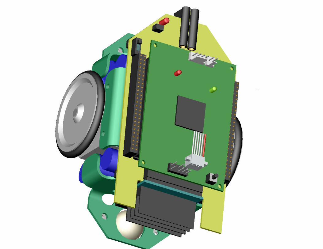
H1 &H2 – Micro-controller plug in location
• Plug micro-controller board in to these headers. • Orientation of micro-controller boards is H1 to H1 and H2 to H2 • Reset switch on micro-controller board will be located at the back of the robot near H2
Rxa & RXB – RF. Comm. Header (Laipac Data Sheets)
# HC12 PIC 1 – Gnd Gnd Gnd
2 – Digital Data Out PS2 RC7 3 – Linear Out NC NC
4 - +5V Controlled by PT3 Controlled by RB5 5 - +5V Controlled by PT3 Controlled by RB5 6 - Gnd Gnd Gnd 7 – Gnd Gnd Gnd
8 - Antenna NC NC SV3- Motor Port (A3967 Stepper Motor Driver Data Sheet)
# HC12 PIC A3967 (pin – des) # HC12 PIC A3967 (pin – des) 1 Gnd Gnd 2 Gnd Gnd 3 Gnd Gnd 4 Gnd Gnd 5 PP1
(AC coupled) RC2
(AC coupled)
24-PFD 6 PT6 RC2 1-REF
7 PA6 RD6 3 -Sleep 8 PA7 RD7 22 - Reset 9 PT5 RB7 10-Step 2nd motor 10 PA5 RD5 11- Dir 2nd motor
11 PA2 RD2 12-MS1 12 PA3 RD3 13 – MS2 13 PT4 RB6 10 – Step 1st motor 14 PA1 RD1 11- Dir 1st motor 15 PAD11 NC 16 PAD10 AN2
(RA2)
17 PAD15 NC 18 PAD12 NC 19 +5V +5V 20 +5V +5V 21 Vadj Vadj 22 Vadj Vadj 23 +12V +12
V 24 +12V +12V
25 Gnd Gnd 26 Gnd Gnd Sensors
# HC12 PIC 1 – IR RX Mod
(Data Sheet) PS0 (Pulled high) RC4 (Pulled high)
2 – Photo Resistor (Data Sheet)
PAD13 AN3 (RA3)
3 – IR Pin Diode (Data Sheet)
PAD03 AN3 (RA3)

Bottom View
2 1 2 1 TX1
JP10 JP11 1 1 TX2 JP1 JP3 ` 1 1
J2 OP1 J2
1 1 1 JP2 JP4 JP8 JP12 S1
1 2 1 2
Side View (from Front) Side View (from Front)
JP1, JP2, JP3, and JP4 – Battery Connectors JP1, JP2, JP3, and JP4 – Battery Connectors • 1 – Negative Terminal • 1 – Negative Terminal • 2 – Positive Terminal • 2 – Positive Terminal • Batteries are connected in series • Batteries are connected in series
JP10 – Sensor Header JP10 – Sensor Header
# # HC12 HC12 PIC PIC # # HC12 HC12 PIC PIC 1 PAD10 AN0
(RA0) 2 PAD11 AN1
(RA1) 3 PAD12 AN2
(RA2) 4 +5V +5V
5 Gnd Gnd 6 Gnd Gnd 7 PT2 RB4 8 PB3 RC3 9 PB4 RC4 10 PB5 RC5
11 +14 +14V 12 +14V +14V JP8 – Sensor Header
# HC12 PIC # HC12 PIC 1 PAD00 AN 0
(RA0) 2 PAD01 AN1
(RA1) 3 PAD02 AN 2
(RA2) 4 +5V +5V
5 Gnd Gnd 6 Gnd Gnd 7 PT2 RB4 8 PH0 RB0 9 PH1 RB1 10 PH2 RB2
11 +14 +14V 12 +14V +14V JP11 – Sensor Header
# HC12 PIC # HC12 PIC 1 PAD05 AN5
(RE0) 2 PAD06 AN6
(RE1) 3 Gnd Gnd) 4 +5V +5V 5 Gnd Gnd 6 Gnd Gnd 7 PT2 RB4 8 PP6 RA4 9 PP7 RA5 10 Gnd Gnd
11 +14 +14V 12 +14V +14V JP12 – Sensor Header
# HC12 PIC # HC12 PIC 1 PAD15 AN5
(RE0) 2 PAD16 AN6
(RE1) 3 Gnd Gnd) 4 +5V +5V 5 Gnd Gnd 6 Gnd Gnd 7 PT2 RB4 8 PP3 RA1 9 PP4 RA2 10 Gnd Gnd
11 +14 +14V 12 +14V +14V
Tx1 – RF. Comm. Header (Laipac Data Sheets) # HC12 PIC 1 +5V +5V 2 +5V +5V 3 Gnd Gnd 4 Gnd Gnd 5 Antenna Antenna
6 - Digital Data Input PS3 RC6 Tx2 – RF. Comm. Header (Laipac Data Sheets)
# HC12 PIC 1 Gnd Gnd
2 – Data In PS3 RC6 3 +5V +5V 4 Antenna Antenna
OP1 – IR Prox. Header(Data Sheets)
# HC12 PIC 1 – Switched +5V PT3 RB5
2 Analogue Gnd Analogue Gnd 3 – prox out to 1.2k to PAD04 to
10k to gnd PAD04 AN4
(RA5) S1 – Switch(Pulled High through 10K)
HC12 PIC PS0 RC4
J2 –Charging Port
• 16V AC, 300mA • Charging LED will light once Batteries reached full charge
Power Sensing HC12 PIC Raw Charging
Terminal PE1 RB0
Logic Low on Full Charge
PE0 NC

MICROSTEPPING DRIVER WITH TRANSLATOR
Always order by complete part number, e.g., A3967SLB .
ABSOLUTE MAXIMUM RATINGSat TA = +25°C
Load Supply Voltage, VBB ............. 30 VOutput Current, IOUT
Continuous ..................... ±750 mA*
Peak ................................ ±850 mALogic Supply Voltage, VCC ........... 7.0 VLogic Input Voltage Range, VIN
(tw >30 ns) .... -0.3 V to VCC + 0.3 V(tw <30 ns) .......... -1 V to VCC + 1 V
Sense Voltage, VSENSE .............. 0.68 VReference Voltage, VREF................. VCC
Package Power Dissipation,PD ......................................... 2.2 W
Operating Temperature Range,TA ........................... -20°C to +85°C
Junction Temperature, TJ ......... +150°CStorage Temperature Range,
TS ......................... -55°C to +150°C* Output current rating may be limited byduty cycle, ambient temperature, and heatsinking. Under any set of conditions, do notexceed the specified current rating or ajunction temperature of 150°C.
Data S
heet26184.24
3967
The A3967SLB is a complete microstepping motor driver withbuilt-in translator. It is designed to operate bipolar stepper motors infull-, half-, quarter-, and eighth-step modes, with output drive capabil-ity of 30 V and ±750 mA. The A3967SLB includes a fixed off-timecurrent regulator that has the ability to operate in slow, fast, or mixedcurrent-decay modes. This current-decay control scheme results inreduced audible motor noise, increased step accuracy, and reducedpower dissipation.
The translator is the key to the easy implementation of theA3967SLB. By simply inputting one pulse on the STEP input themotor will take one step (full, half, quarter, or eighth depending on twologic inputs). There are no phase-sequence tables, high-frequencycontrol lines, or complex interfaces to program. The A3967SLBinterface is an ideal fit for applications where a complex µP is unavail-able or over-burdened.
Internal circuit protection includes thermal shutdown with hyster-esis, under-voltage lockout (UVLO) and crossover-current protection.Special power-up sequencing is not required.
The A3967SLB is supplied in a 24-lead SOIC with copper batwingtabs. The tabs are at ground potential and need no insulation.
FEATURES ±750 mA, 30 V Output Rating Satlington™ Sink Drivers Automatic Current-Decay Mode Detection/Selection 3.0 V to 5.5 V Logic Supply Voltage Range Mixed, Fast, and Slow Current-Decay Modes Internal UVLO and Thermal Shutdown Circuitry
Crossover-Current Protection
PRELIMINARY INFORMATION(Subject to change without notice)
June 20, 2002
LOADSUPPLY1
SLEEP
ENABLE
OUT1A
GND
STEP
OUT1B
RESET
LOADSUPPLY2
SENSE1
DIR
OUT2A
PFD
RC1
REF÷8
RC2
LOGICSUPPLY
OUT2B
MS2MS1
SENSE2
PWMTIMER
TRANSLATOR& CONTROL
LOGIC
VBB2 VBB1
VCC
Dwg. PP-075-2
23
178
1
2
3
4
5
6
7
9
12
16
15
14
13
24
22
21
20
19
18
11
10
9
GND
GND
GND

115 Northeast Cutoff, Box 15036Worcester, Massachusetts 01615-0036 (508) 853-5000
3967MICROSTEPPING DRIVERWITH TRANSLATOR
2
Copyright © 2002 Allegro MicroSystems, Inc.
FUNCTIONAL BLOCK DIAGRAM
Table 1. Microstep Resolution Truth Table
MS1 MS2 ResolutionL L Full step (2 phase)H L Half stepL H Quarter stepH H Eighth step
1918
SENSE1
VBB1
VBB2
OUT1A
OUT1B
OUT2A
OUT2B
SENSE2
5
9
20
16
21
17
8
4
TR
AN
SLA
TO
R
LOADSUPPLY
Dwg. FP-050-3
PWM TIMER
PWM TIMER
PWM LATCHBLANKINGMIXED DECAY
CO
NT
RO
L LO
GIC
UVLO AND
FAULTDETECT
DAC
+ -
+ -DAC
SENSE
PWM LATCHBLANKINGMIXED DECAY
3
3
REF
LOGICSUPPLY
VCC
STEP
DIR
MS1
SLEEP
MS2
ENABLE
RC1
RESET
PFD
RC2
REF.SUPPLY
VPF
÷8
14
1
23
10
11
22
12
13
3
15
5
2
76

3967MICROSTEPPING DRIVER
WITH TRANSLATOR
www.allegromicro.com 3
ELECTRICAL CHARACTERISTICS at TA = +25°C, VBB = 30 V, VCC = 3.0 V to 5.5V (unless otherwisenoted)
Limits
Characteristic Symbol Test Conditions Min. Typ. Max. Units
Output Drivers
Load Supply Voltage Range VBB Operating 4.75 – 30 V
During sleep mode 0 – 30 V
Output Leakage Current ICEX VOUT = VBB – <1.0 20 µA
VOUT = 0 V – <-1.0 -20 µA
Output Saturation Voltage VCE(sat) Source driver, IOUT = -750 mA – – 2.1 V
Source driver, IOUT = -400 mA – – 2.0 V
Sink driver, IOUT = 750 mA – – 1.3 V
Sink driver, IOUT = 400 mA – – 0.5 V
Clamp Diode Forward Voltage VF IF = 750 mA – 1.4 1.6 V
IF = 400 mA – 1.1 1.4 V
Motor Supply Current IBB Outputs enabled – – 5.0 mA
RESET high – – 200 µA
Sleep mode – – 20 µA
Control Logic
Logic Supply Voltage Range VDD Operating 3.0 5.0 5.5 V
Logic Input Voltage VIN(1) 0.7VDD – – V
VIN(0) – – 0.3VDD V
Logic Input Current IIN(1) VIN = 0.7VDD -20 <1.0 20 µA
IIN(0) VIN = 0.3VDD -20 <1.0 20 µA
Maximum STEP Frequency fSTEP 500* – – kHz
Blank Time tBLANK Rt = 56 kΩ, Ct = 680 pF 700 950 1200 ns
Fixed Off Time toff Rt = 56 kΩ, Ct = 680 pF 30 38 46 µs
continued next page …

115 Northeast Cutoff, Box 15036Worcester, Massachusetts 01615-0036 (508) 853-5000
3967MICROSTEPPING DRIVERWITH TRANSLATOR
4
ELECTRICAL CHARACTERISTICS at TA = +25°C, VCC = 30 V, VDD = 3.0 V to 5.5V (unless otherwisenoted)
Limits
Characteristic Symbol Test Conditions Min. Typ. Max. Units
Control Logic (cont’d)
Mixed Decay Trip Point PFDH – 0.6VCC – V
PFDL – 0.21VCC – V
Ref. Input Voltage Range VREF Operating 1.0 – VCC V
Reference Input Impedance ZREF 120 160 200 kΩ
Gain (Gm) Error EG VREF = 2 V, Step = 3† – – ±10 %
(note 3) VREF = 2 V, Step = 5† – – ±5.0 %
VREF = 2 V, Step = 9† – – ±5.0 %
Thermal Shutdown Temp. TJ – 165 – °C
Thermal Shutdown Hysteresis ∆TJ – 15 – °C
UVLO Enable Threshold VUVLO Increasing VDD 2.45 2.7 2.95 V
UVLO Hysteresis ∆VUVLO 0.05 0.10 – V
Logic Supply Current IDD Outputs enabled – 65 85 mA
Outputs off – – 9.0 mA
Sleep mode – – 100 µA
* Operation at a step frequency greater than the specified minimum value is possible but not warranteed.† 8 microstep/step operation.NOTES: 1. Typical Data is for design information only.
2. Negative current is defined as coming out of (sourcing) the specified device terminal.3. EG = ([VREF/8] – VSENSE)/(VREF/8)

3967MICROSTEPPING DRIVER
WITH TRANSLATOR
www.allegromicro.com 5
Device Operation. The A3967 is a completemicrostepping motor driver with built in translator foreasy operation with minimal control lines. It is designedto operate bipolar stepper motors in full-, half-, quarter-and eighth-step modes. The current in each of the twooutput H-bridges is regulated with fixed off time pulse-width modulated (PWM) control circuitry. The H-bridgecurrent at each step is set by the value of an externalcurrent sense resistor (RS), a reference voltage (VREF), andthe DAC’s output voltage controlled by the output of thetranslator.
At power up, or reset, the translator sets the DACs andphase current polarity to initial home state (see figures forhome-state conditions), and sets the current regulator forboth phases to mixed-decay mode. When a step commandsignal occurs on the STEP input the translator automati-cally sequences the DACs to the next level (see table 2 forthe current level sequence and current polarity). Themicrostep resolution is set by inputs MS1 and MS2 asshown in table 1. If the new DAC output level is lowerthan the previous level the decay mode for that H-bridgewill be set by the PFD input (fast, slow or mixed decay).If the new DAC level is higher or equal to the previouslevel then the decay mode for that H-bridge will be slowdecay. This automatic current-decay selection willimprove microstepping performance by reducing thedistortion of the current waveform due to the motorBEMF.
Reset Input (RESET). The RESET input (active low)sets the translator to a predefined home state (see figuresfor home state conditions) and turns off all of the outputs.STEP inputs are ignored until the RESET input goes high.
Step Input (STEP). A low-to-high transition on theSTEP input sequences the translator and advances themotor one increment. The translator controls the input tothe DACs and the direction of current flow in each wind-ing. The size of the increment is determined by the stateof inputs MS1 and MS2 (see table 1).
Microstep Select (MS1 and MS2). Input terminalsMS1 and MS2 select the microstepping format pertable 1. Changes to these inputs do not take effect untilthe STEP command (see figure).
Direction Input (DIR). The state of the DIRECTIONinput will determine the direction of rotation of the motor.
Internal PWM Current Control. Each H-bridge iscontrolled by a fixed off time PWM current-control circuitthat limits the load current to a desired value (ITRIP).Initially, a diagonal pair of source and sink outputs areenabled and current flows through the motor winding andRS. When the voltage across the current-sense resistorequals the DAC output voltage, the current-sense com-parator resets the PWM latch, which turns off the sourcedriver (slow-decay mode) or the sink and source drivers(fast- or mixed-decay modes).
The maximum value of current limiting is set by theselection of RS and the voltage at the VREF input with atransconductance function approximated by:
ITRIPmax = VREF/8RS
The DAC output reduces the VREF output to thecurrent-sense comparator in precise steps (see table 2 for% ITRIPmax at each step).
ITRIP = (% ITRIPmax/100) x ITRIPmax
Fixed Off-Time. The internal PWM current-controlcircuitry uses a one shot to control the time the driver(s)remain(s) off. The one shot off-time, toff, is determined bythe selection of an external resistor (RT) and capacitor(CT) connected from the RC timing terminal to ground.The off time, over a range of values of CT = 470 pF to1500 pF and RT = 12 kΩ to 100 kΩ is approximated by:
toff = RTCT
Functional Description

115 Northeast Cutoff, Box 15036Worcester, Massachusetts 01615-0036 (508) 853-5000
3967MICROSTEPPING DRIVERWITH TRANSLATOR
6
RC Blanking. In addition to the fixed off time of thePWM control circuit, the CT component sets the compara-tor blanking time. This function blanks the output of thecurrent-sense comparator when the outputs are switchedby the internal current-control circuitry. The comparatoroutput is blanked to prevent false over-current detectiondue to reverse recovery currents of the clamp diodes, and/or switching transients related to the capacitance of theload. The blank time tBLANK can be approximated by:
tBLANK = 1400CT
Enable Input (ENABLE). This active-low inputenables all of the outputs. When logic high the outputs aredisabled. Inputs to the translator (STEP, DIRECTION,MS1, MS2) are all active independent of the ENABLEinput state.
Shutdown. In the event of a fault (excessive junctiontemperature) the outputs of the device are disabled untilthe fault condition is removed. At power up, and in theevent of low VCC, the under-voltage lockout (UVLO)circuit disables the drivers and resets the translator to thehome state.
Sleep Mode (SLEEP). An active-low control inputused to minimize power consumption when not in use.This disables much of the internal circuitry including theoutputs. A logic high allows normal operation and startupof the device in the home position.
Percent Fast Decay Input (PFD). When a STEPinput signal commands a lower output current from theprevious step, it switches the output current decay to eitherslow-, fast-, or mixed-decay depending on the voltagelevel at the PFD input. If the voltage at the PFD input isgreater than 0.6VDD then slow-decay mode is selected. Ifthe voltage on the PFD input is less than 0.21VDD thenfast-decay mode is selected. Mixed decay is betweenthese two levels.
Mixed Decay Operation. If the voltage on the PFDinput is between 0.6VDD and 0.21VDD, the bridge willoperate in mixed-decay mode depending on the stepsequence (see figures). As the trip point is reached, thedevice will go into fast-decay mode until the voltage onthe RC terminal decays to the voltage applied to the PFDterminal. The time that the device operates in fast decay isapproximated by:
tFD = RTCTIn (0.6VDD/VPFD)
After this fast decay portion, tFD, the device willswitch to slow-decay mode for the remainder of the fixedoff-time period.
Functional Description (cont’d)

3967MICROSTEPPING DRIVER
WITH TRANSLATOR
www.allegromicro.com 7
Timing Requirements(TA = +25°C, VCC = 5 V, Logic Levels are VCC and Ground)
A B
C D
50%STEP
MS1/MS2/DIR/RESET
Dwg. WP-042
SLEEP
E
A. Minimum Command Active TimeBefore Step Pulse (Data Set-Up Time) ..... 200 ns
B. Minimum Command Active TimeAfter Step Pulse (Data Hold Time)............ 200 ns
C. Minimum STEP Pulse Width ...................... 1.0 µs
D. Minimum STEP Low Time ......................... 1.0 µs
E. Maximum Wake-Up Time ......................... 1.0 ms

115 Northeast Cutoff, Box 15036Worcester, Massachusetts 01615-0036 (508) 853-5000
3967MICROSTEPPING DRIVERWITH TRANSLATOR
8
Layout. The printed wiring board should use a heavyground plane.
For optimum electrical and thermal performance, thedriver should be soldered directly onto the board.
The load supply terminal, VBB, should be decoupledwith an electrolytic capacitor (>47 µF is recommended)placed as close to the device as possible.
To avoid problems due to capacitive coupling of thehigh dv/dt switching transients, route the bridge-outputtraces away from the sensitive logic-input traces. Alwaysdrive the logic inputs with a low source impedance toincrease noise immunity.
Grounding. A star ground system located close to thedriver is recommended.
The 24-lead SOIC has the analog ground and thepower ground internally bonded to the power tabs of thepackage (leads 6, 7, 18, and 19).
Applications Information
Current Sensing. To minimize inaccuracies caused byground-trace IR drops in sensing the output current level,the current-sense resistor (RS) should have an independentground return to the star ground of the device. This pathshould be as short as possible. For low-value senseresistors the IR drops in the printed wiring board senseresistor’s traces can be significant and should be takeninto account. The use of sockets should be avoided asthey can introduce variation in RS due to their contactresistance.
Allegro MicroSystems recommends a value of RS
given by
RS = 0.5/ITRIPmax
Thermal protection. Circuitry turns off all driverswhen the junction temperature reaches 165°C, typically.It is intended only to protect the device from failures dueto excessive junction temperatures and should not implythat output short circuits are permitted. Thermal shut-down has a hysteresis of approximately 15°C.
50 75 100 125 150
2.5
1.5
1.0
0.5
0
TEMPERATURE in °°°°C
2.0
25
Dwg. GP-019C
R = 6°C/W θJT
R = 77°C/W θJA
AL
LO
WA
BL
E P
AC
KA
GE
PO
WE
R D
ISS
IPA
TIO
N in
WA
TT
S
R = 49°C/W θJARθJA is measured on typical two-sided PCB with minimal copper
ground area (77°C/W) or with3.57 in2 copper ground area
(49°C/W). See also, ApplicationNote 29501.5, Improving
Batwing Power Dissipation.

3967MICROSTEPPING DRIVER
WITH TRANSLATOR
www.allegromicro.com 9
Table 2. Step Sequencing(DIR = L)
Phase 2 Phase 1Full Half Quarter Eighth Current Current Step
Step # Step # Step # Step # [%Itripmax] [%Itripmax] Angle
1 1 1 0.00 100.00 02 19.51 98.08 11.25
2 3 38.27 92.39 22.504 55.56 83.15 33.75
1 2 3 5 70.71 70.71 45*6 83.15 55.56 56.25
4 7 92.39 38.27 67.508 98.08 19.51 78.75
3 5 9 100.00 0.00 9010 98.08 -19.51 101.25
6 11 92.39 -38.27 112.5012 83.15 -55.56 123.75
2 4 7 13 70.71 -70.71 13514 55.56 -83.15 146.25
8 15 38.27 -92.39 157.5016 19.51 -98.08 168.75
5 9 17 0.00 -100.00 18018 -19.51 -98.08 191.25
10 19 -38.27 -92.39 202.5020 -55.56 -83.15 213.75
3 6 11 21 -70.71 -70.71 22522 -83.15 -55.56 236.25
12 23 -92.39 -38.27 247.5024 -98.08 -19.51 258.75
7 13 25 -100.00 0.00 27026 -98.08 19.51 281.25
14 27 -92.39 38.27 292.5028 -83.15 55.56 303.75
4 8 15 29 -70.71 70.71 31530 -55.56 83.15 326.25
16 31 -38.27 92.39 337.5032 -19.51 98.08 348.75
9 17 33 0.00 100.00 360
* Home state.

115 Northeast Cutoff, Box 15036Worcester, Massachusetts 01615-0036 (508) 853-5000
3967MICROSTEPPING DRIVERWITH TRANSLATOR
10
Dwg. WK-004-19
PHASE 1CURRENT
PHASE 2CURRENT
STEPINPUT
SLOWDECAY
70.7%
–70.7%
70.7%
–70.7%
SLOWDECAY
Full Step OperationMS1 = MS2 = L, DIR = H
The vector addition of the output currents at any step is100%.

3967MICROSTEPPING DRIVER
WITH TRANSLATOR
www.allegromicro.com 11
Dwg. WK-004-18
PHASE 1CURRENT
PHASE 2CURRENT
STEPINPUT
SLO
WD
EC
AY
MIX
ED
DE
CA
Y
SLO
WD
EC
AY
MIX
ED
DE
CA
Y100%
–100%
100%
–100%
SLO
WD
EC
AY
MIX
ED
DE
CA
Y
SLO
WD
EC
AY
MIX
ED
DE
CA
Y
SLO
WD
EC
AY
MIX
ED
DE
CA
Y
SLO
WD
EC
AY
MIX
ED
DE
CA
Y
SLO
WD
EC
AY
MIX
ED
DE
CA
Y
SLO
WD
EC
AY
MIX
ED
DE
CA
Y
70.7%
–70.7%
70.7%
70.7%
Half Step OperationMS1 = H, MS2 = L, DIR = H
The mixed-decay mode is controlled by the percent fastdecay voltage (VPFD). If the voltage at the PFD input isgreater than 0.6VDD then slow-decay mode is selected. Ifthe voltage on the PFD input is less than 0.21VDD thenfast-decay mode is selected. Mixed decay is betweenthese two levels.

115 Northeast Cutoff, Box 15036Worcester, Massachusetts 01615-0036 (508) 853-5000
3967MICROSTEPPING DRIVERWITH TRANSLATOR
12
Dwg. WK-004-17
PHASE 1CURRENT
PHASE 2CURRENT
STEPINPUT
SLOWDECAY
MIXEDDECAY
SLOWDECAY
MIXEDDECAY
100%
–100%
100%
–100%
SLOWDECAY
MIXEDDECAY
SLOWDECAY
MIXEDDECAY
38.3%
70.7%
–70.7%
70.7%
–70.7%
–38.3%
38.3%
–38.3%
Quarter Step OperationMS1 = L, MS2 = H, DIR = H
The mixed-decay mode is controlled by the percent fastdecay voltage (VPFD). If the voltage at the PFD input isgreater than 0.6VDD then slow-decay mode is selected. Ifthe voltage on the PFD input is less than 0.21VDD thenfast-decay mode is selected. Mixed decay is betweenthese two levels.

3967MICROSTEPPING DRIVER
WITH TRANSLATOR
www.allegromicro.com 13
Dwg. WK-004-16
PHASE 2CURRENT
100%
–100%
SLOWDECAY
MIXEDDECAY
SLOWDECAY
MIXEDDECAY
PHASE 1CURRENT
STEPINPUT
SLOWDECAY
MIXEDDECAY
SLOWDECAY
MIXEDDECAY
100%
–100%
70.7%
38.3%
–70.7%
–38.3%
70.7%
38.3%
–70.7%
–38.3%
8 Microstep/Step OperationMS1 = MS2 = H, DIR = H
The mixed-decay mode is controlled by the percent fastdecay voltage (VPFD). If the voltage at the PFD input isgreater than 0.6VDD then slow-decay mode is selected. Ifthe voltage on the PFD input is less than 0.21VDD thenfast-decay mode is selected. Mixed decay is betweenthese two levels.
115 Northeast Cutoff, Box 15036Worcester, Massachusetts 01615-0036 (508) 853-5000
3967MICROSTEPPING DRIVERWITH TRANSLATOR
14
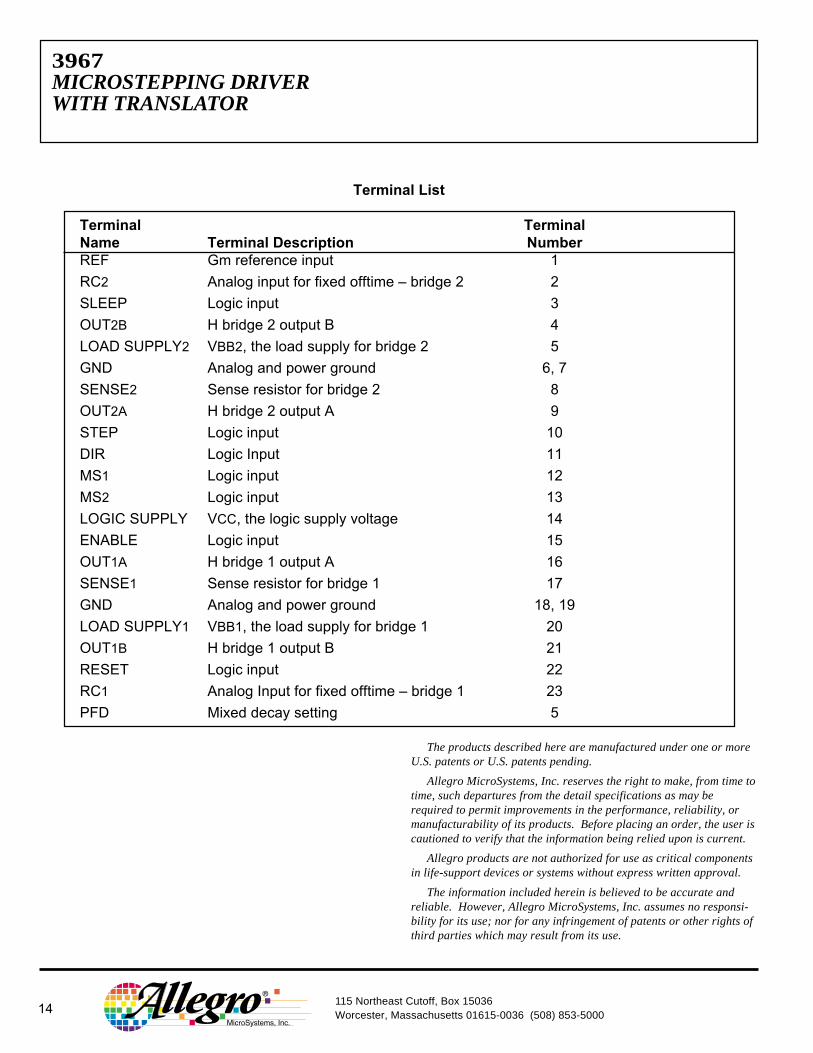
Terminal List
Terminal TerminalName Terminal Description NumberREF Gm reference input 1
RC2 Analog input for fixed offtime – bridge 2 2
SLEEP Logic input 3
OUT2B H bridge 2 output B 4
LOAD SUPPLY2 VBB2, the load supply for bridge 2 5
GND Analog and power ground 6, 7
SENSE2 Sense resistor for bridge 2 8
OUT2A H bridge 2 output A 9
STEP Logic input 10
DIR Logic Input 11
MS1 Logic input 12
MS2 Logic input 13
LOGIC SUPPLY VCC, the logic supply voltage 14
ENABLE Logic input 15
OUT1A H bridge 1 output A 16
SENSE1 Sense resistor for bridge 1 17
GND Analog and power ground 18, 19
LOAD SUPPLY1 VBB1, the load supply for bridge 1 20
OUT1B H bridge 1 output B 21
RESET Logic input 22
RC1 Analog Input for fixed offtime – bridge 1 23
PFD Mixed decay setting 5
The products described here are manufactured under one or moreU.S. patents or U.S. patents pending.
Allegro MicroSystems, Inc. reserves the right to make, from time totime, such departures from the detail specifications as may berequired to permit improvements in the performance, reliability, ormanufacturability of its products. Before placing an order, the user iscautioned to verify that the information being relied upon is current.
Allegro products are not authorized for use as critical componentsin life-support devices or systems without express written approval.
The information included herein is believed to be accurate andreliable. However, Allegro MicroSystems, Inc. assumes no responsi-bility for its use; nor for any infringement of patents or other rights ofthird parties which may result from its use.

3967MICROSTEPPING DRIVER
WITH TRANSLATOR
www.allegromicro.com 15
NOTES: 1. Exact body and lead configuration at vendor’s option within limits shown.2. Lead spacing tolerance is non-cumulative.3. Webbed lead frame. Leads 6, 7, 18, and 19 are internally one piece.4. Supplied in standard sticks/tubes of 31 devices or add “TR” to part number for tape and reel.
0° TO 8°1 2 3
0.29920.2914
0.61410.5985
0.4190.394
0.0200.013
.0926
.1043
0.0040 MIN.
0.01250.0091
Dwg. MA-008-25A in
0.050BSC
24 13
NOTE 1NOTE 3
0.0500.016
0° TO 8°1 2 3
7.607.40
15.6015.20
10.6510.00
0.510.33
.65
.35
0.10 MIN.
0.320.23
Dwg. MA-008-25A mm
1.27BSC
24 13
NOTE 1NOTE 3
1.270.40
Dimensions in Inches(for reference only)
Dimensions in Millimeters(controlling dimensions)

115 Northeast Cutoff, Box 15036Worcester, Massachusetts 01615-0036 (508) 853-5000
3967MICROSTEPPING DRIVERWITH TRANSLATOR
16
MOTOR DRIVERSFunction Output Ratings* Part Number†
INTEGRATED CIRCUITS FOR BRUSHLESS DC MOTORS3-Phase Power MOSFET Controller — 28 V 39333-Phase Power MOSFET Controller — 50 V 39323-Phase Back-EMF Controller/Driver ±900 mA 14 V 8902–A
INTEGRATED BRIDGE DRIVERS FOR DC AND BIPOLAR STEPPER MOTORSDual Full Bridge with Protection & Diagnostics ±500 mA 30 V 3976PWM Current-Controlled Dual Full Bridge ±650 mA 30 V 3966PWM Current-Controlled Dual Full Bridge ±650 mA 30 V 3968Microstepping Translator/Dual Full Bridge ±750 mA 30 V 3967PWM Current-Controlled Dual Full Bridge ±750 mA 45 V 2916PWM Current-Controlled Dual Full Bridge ±750 mA 45 V 2919PWM Current-Controlled Dual Full Bridge ±750 mA 45 V 6219PWM Current-Controlled Dual Full Bridge ±800 mA 33 V 3964PWM Current-Controlled Dual DMOS Full Bridge ±1.0 A 35 V 3973PWM Current-Controlled Full Bridge ±1.3 A 50 V 3953PWM Current-Controlled Dual Full Bridge ±1.5 A 45 V 2917PWM Current-Controlled DMOS Full Bridge ±1.5 A 50 V 3948PWM Current-Controlled Microstepping Full Bridge ±1.5 A 50 V 3955PWM Current-Controlled Microstepping Full Bridge ±1.5 A 50 V 3957PWM Current-Controlled Dual DMOS Full Bridge ±1.5 A 50 V 3972PWM Current-Controlled Dual DMOS Full Bridge ±1.5 A 50 V 3974PWM Current-Controlled Full Bridge ±2.0 A 50 V 3952PWM Current-Controlled DMOS Full Bridge ±2.0 A 50 V 3958Microstepping Translator/Dual DMOS Full Bridge ±2.5 A 35 V 3977Dual DMOS Full Bridge ±2.5 A 50 V 3971PWM Current-Controlled DMOS Full Bridge ±3.0 A 50 V 3959
UNIPOLAR STEPPER MOTOR & OTHER DRIVERSUnipolar Stepper-Motor Quad Drivers 1.0 A 46 V 7024 & 7029Unipolar Microstepper-Motor Quad Driver 1.2 A 46 V 7042Unipolar Stepper-Motor Translator/Driver 1.25 A 50 V 5804Unipolar Stepper-Motor Quad Driver 1.8 A 50 V 2540Unipolar Stepper-Motor Quad Driver 3.0 A 46 V 7026
Unipolar Microstepper-Motor Quad Driver 3.0 A 46 V 7044
* Current is maximum specified test condition, voltage is maximum rating. See specification for sustaining voltage limitsor over-current protection voltage limits. Negative current is defined as coming out of (sourcing) the output.
† Complete part number includes additional characters to indicate operating temperature range and package style.
Also, see 3175, 3177, 3235, and 3275 Hall-effect sensors for use with brushless dc motors.

Datasheet -- SDP8436-003
Representative photograph, actual product appearance may vary.
Dimensions
Schematic
Performance Charts
Specifications
Click here for a print friendly version of this datasheet.
SDP8436-003
SDP Series Silicon PhotoTransistor, Side-looking Plastic Package
Features
Side-looking plastic package 18 ° (nominal) acceptance angle Enhanced coupling distance Internal visible light rejection filter Low profile for design flexibility Wide sensitivity ranges Mechanically matched to SEP8736 infrared emitting diodes
Description
The SDP8436 is an NPN silicon phototransistor molded in a black plastic package which combines the mounting advantages of a side-looking package with the narrow acceptance angle and high optical gain of a T-1 package. The SDP8436 is designed for those applications which require longer coupling distances than standard side-looking devices can provide, such as touch screens. The device is also well suited to applications in which adjacent channel crosstalk could be a problem. The package is highly transmissive to the IR source energy while it provides effective shielding against visible ambient light.
http://catalog.sensing.honeywell.com/datasheet.asp?FAM=infrared&PN=SDP8436%2D003 (1 of 2) [2003/04/22 11:26:56 AM]

Datasheet -- SDP8436-003
Product Specifications
Product Type IR Component
Angular Response (Degree) 18
Light Current Minimum 7.0 mA
Light Current Maximum 17.5 mA
Package Style Side-Looking
Package Components Plastic
Package Color Black
Rise and Fall Time 15 µs
Power Dissipation 100 mW
Operating Temperature Range -40 °C to 85 °C [-40 °F to 185 °F]
Dark Current 100 nA
Collector-Emitter Breakdown Voltage 30 V
Emitter-Collector Breakdown Voltage 5 V
Collector-Emitter Saturation Voltage 0.4 V
Comment The radiation source is a tungsten lamp operating at a color temperature of 2870°K.
Availability Global
Product Name Phototransistor
Due to regional agency approval requirements, some products may not be available in your area.Please contact your regional Honeywell office regarding your product of choice.
Top of Page
© Copyright Honeywell Inc.1998 - 2003 All rights reserved.
Please send comments to [email protected]
http://catalog.sensing.honeywell.com/datasheet.asp?FAM=infrared&PN=SDP8436%2D003 (2 of 2) [2003/04/22 11:26:56 AM]

http://catalog.sensing.honeywell.com/Author/Images/honeywell/ir/dim_019.gif
http://catalog.sensing.honeywell.com/Author/Images/honeywell/ir/dim_019.gif [2003/04/22 11:27:00 AM]

http://catalog.sensing.honeywell.com/Author/Images/honeywell/ir/sch_002.gif
http://catalog.sensing.honeywell.com/Author/Images/honeywell/ir/sch_002.gif [2003/04/22 11:27:04 AM]

Silicon PhototransistorSDP8436
SWITCHING TIME TEST CIRCUITcir_015.cdr
SWITCHING WAVEFORMcir_004.cdr
Responsivity vsAngular Displacement gra_013.ds4
Angular displacement - degrees
Rel
ativ
e re
spon
se
0.0
0.1
0.2
0.3 0.4
0.5
0.6
0.7
0.8 0.9
1.0
-40 -30 -20 -10 0 +10 +20 +30 +40
Fig. 1 Collector Current vsAmbient Temperature gra_039.ds4
Ambient temperature - °C
Nor
mal
ized
col
lect
or
curr
ent
0.0
0.4
0.8
1.2
1.6
2.0
0 10 20 30 40 50 60 70 80
Fig. 2
Dark Current vsTemperature gra_301.cdr
Fig. 3 Non-Saturated Switching Time vsLoad Resistance gra_041.ds4
Load resistance - Ohms
Res
pons
e tim
e -
µs
1
10
100
10 100 1000 10000
Fig. 4
Honeywell reserves the right to make changes in order to improve design and supply the best products possible.
h130

Silicon PhototransistorSDP8436
Spectral Responsivity gra_050.ds4
Wavelength - nm
Rel
ativ
e re
spon
se
0.0
0.10.2
0.30.4
0.50.6
0.7
0.8
0.9
1.0
600 700 800 900 1000 1100 1200
Fig. 5 Coupling Characteristicswith SEP8736 gra_034.ds4
Lens-to-lens separation - inches
Nor
mal
ized
ligh
t cu
rren
t
0.001
0.1
1.0
10
0.1 1.0 10
0.01
Fig. 6
All Performance Curves Show Typical Values
Honeywell reserves the right to make changes in order to improve design and supply the best products possible.
h 131

ELECTRO-OPTICAL CHARACTERISTICS TA=25OC (2 HOURS LIGHT ADAPT, MIN)***
MODEL NO.CELL RESISTANCE** (Ohms) SENSITIVITY SPECTRAL PEAK RESPONSE TIME @10 Lux
10 Lux @2856K DARK LOG(R100)-LOG(R10) (nm) RISE TIME (ms) FALL TIME (ms)
MIN (KWW ) MAX (KWW ) MIN (MWW ) SEC (ll TYP) TYP TYP TYP
PDV-P9001 4 11 0.3 10 0.65 520 60 25
PDV-P9002 9 20 0.5 10 0.6 520 60 25
PDV-P9002-1 11 20 0.5 10 0.7 520 60 25
PDV-P9003 16 33 1 10 0.8 520 60 25
PDV-P9003-1 23 33 1 10 0.85 520 60 25
PDV-P9004 27 60 2 10 0.85 520 60 25
PDV-P9005 50 94 2.5 10 0.9520 60 25
PDV-P9005-1 48 140 20 10 0.9 520 60 25
ABSOLUTE MAXIMUM RATING (TA=25OC unless otherwise noted)
SYMBOL PARAMETER MIN MAX UNITS
V PK Applied Voltage 150 V dc
Pd po/ t Continuous Power Dissipation 90 mW OC
Tstg & To Operating Temperature Range & Storage -30 +75 OC
TS Soldering Temperature* +260 OC*.200 inch (5 mm) from bottom of header for 3 secs max with heat sink
FEATURESVisible light responseSintered constructionLow costHigh Reliability
Cadmium Sulfoselenide (CdS) Photoconductive PhotocellsType PDV-P9XXX-X
APPLICATIONSCamera exposureLow light levelShutter controlsNight light controls
Information in this technical data sheet is believed to be correct and reliable. However, no responsibility is assumed for possible inaccuracies or omission. Specificationsare subject to change without notice. ** Photocells are light adapted at 100 to 500 Lux. *** Photocells are tested at 2856 oK at a 10 Luxlight level. Resistance values are for reference only. PAGE 1 OF 2
[FORM NO. 100-PDV-P9001 REV A]
DESCRIPTIONPDV-P9XXX-X are (CdS) photoconductivephotocells designed to sense light from 400nm to 700 nm. As light dependent resistors,they are available in a wide range of resis-tance values. They are packaged in a twoleaded plastic-coated ceramic header.
K
Oh
ms
PHOTONICDETECTORS INC.
PACKAGE DIMENSIONS INCH [mm]
1. PHOTOCELL "GRID" PATTERN CAN VARY, PDI RESERVES THE RIGHT TO CHANGE AND MIX GRID PATTERNS.2. DIMENSION CONTROLLED AT BASE OF CERAMIC HEADER PACKAGE.
PLASTIC COATED CERAMIC PACKAGE
LOG (E100)-LOG(E10)
CELL RESISTANCE VS. ILLUMINANCE
Lux
.138 [3.50] .079 [2.00]
1.023 [26.0] MIN
2X Ø.016 [0.40]
.100 [2.54]
EPOXY ON LEADS 3mm MAX
Ø.165 [4.20]
+.015 [0.38]-.010 [0.25]
±.010 [0.25]
±.010 [0.25]
1
2PLASTICCOATED
INDUSTRY EQUIVALENTS:VT900 & NSL5152

ELECTRO-OPTICAL CHARACTERISTICS TA=25OC (2 HOURS LIGHT ADAPT, MIN)***
MODEL NO.CELL RESISTANCE** (Ohms) SENSITIVITY SPECTRAL PEAK RESPONSE TIME @10 Lux
10 Lux @2856K DARK LOG(R100)-LOG(R10) (nm) RISE TIME (ms) FALL TIME (ms)
MIN (KWW ) MAX (KWW ) MIN (MWW ) SEC (llTYP) TYP TYP TYP
PDV-P9006 80 200 5 10 1 520 60 25
PDV-P9007 10 100 1 10 0.8 520 60 25
PDV-P9008 10 200 20 10 0.85 520 60 25
PDV-P9103 20 45 1 10 0.8 520 60 25
PDV-P9200 10 50 5 10 0.9 520 70 15
PDV-P9203 5 20 20 10 0.9 520 70 15
ABSOLUTE MAXIMUM RATING (TA=25OC unless otherwise noted)
SYMBOL PARAMETER MIN MAX UNITS
V PK Applied Voltage 150 V dc
Pd po/ t Continuous Power Dissipation 90 mW OC
Tstg & To Operating Temperature Range & Storage -30 +75 OC
TS Soldering Temperature* +260 OC*.200 inch (5 mm) from bottom of header for 3 secs max with heat sink
FEATURESVisible light responseSintered constructionLow costHigh Reliability
Cadmium Sulfoselenide (CdS) Photoconductive Photocells Type PDV-P9XXX-X
Information in this technical data sheet is believed to be correct and reliable. However, no responsibility is assumed for possible inaccuracies or omission. Specificationsare subject to change without notice. ** Photocells are light adapted at 100 to 500 Lux. *** Photocells are tested at 2856 oK at a 10 Luxlight level. Resistance values are for reference only. PAGE 2 OF 2
[FORM NO. 100-PDV-P9001 REV A]
DESCRIPTIONPDV-P9XXX-X are (CdS) photoconductivephotocells designed to sense light from 400nm to 700 nm. As light dependent resistors,they are available in a wide range of resis-tance values. They are packaged in a twoleaded plastic-coated ceramic header.
K
Oh
ms
PHOTONICDETECTORS INC.
PACKAGE DIMENSIONS INCH [mm]
PLASTIC COATED CERAMIC PACKAGE
Camera exposure Low light level
Shutter controls
Night light controls
LOG (E100)-LOG(E10)
APPLICATIONS
1. PHOTOCELL "GRID" PATTERN CAN VARY, PDI RESERVES THE RIGHT TO CHANGE AND MIX GRID PATTERNS.2. DIMENSION CONTROLLED AT BASE OF CERAMIC HEADER PACKAGE.
CELL RESISTANCE VS. ILLUMINANCE
Lux
.138 [3.50] .079 [2.00]
1.023 [26.0] MIN
2X Ø.016 [0.40]
.100 [2.54]
EPOXY ON LEADS 3mm MAX
Ø.165 [4.20]
+.015 [0.38]-.010 [0.25]
±.010 [0.25]
±.010 [0.25]
1
2PLASTICCOATED
INDUSTRY EQUIVALENTS:VT900 & NSL5152

TLP434A & RLP434A RF ASK Hybrid Modules for Radio Control ( New Version )
Laipac Technology, Inc. 105 West Beaver Creek Rd. Unit 207 Richmond Hill Ontario L4B 1C6 Canada Tel: (905)762-1228 Fax: (905)763-1737 e-mail: [email protected]
Symbol Parameter Conditions Min Typ Max Unit
Vcc Operating supply voltage 2.0 - 12.0 V Icc 1 Peak Current (2V) - - 1.64 mA Icc 2 Peak Current (12V) - - 19.4 mA Vh Input High Voltage Idata= 100uA (High) Vcc-0.5 Vcc Vcc+0.5 V Vl Input Low Voltage Idata= 0 uA (Low) - - 0.3 V FO Absolute Frequency 315Mhz module 314.8 315 315.2 MHz PO RF Output Power- 50ohm Vcc = 9V-12V - 16 - dBm
Vcc = 5V-6V - 14 - dBm DR Data Rate External Encoding 512 4.8K 200K bps
Notes : ( Case Temperature = 25°C +- 2°C , Test Load Impedance = 50 ohm ) Application Circuit : Typical Key-chain Transmitter using HT12E-18DIP, a Binary 12 bit Encoder from Holtek Semiconductor Inc.
Application Circuit : Typical RF Receiver using HT12D-18DIP, a Binary 12 bit Decoder with 8 bit uC HT48RXX from Holtek Semiconductor Inc.
Easy-Link Wireless
Symbol Parameter Conditions Min Typ Max
Vcc Operating supply voltage 3.3 5.0V 6.0 V Itot Operating Current - 4.5 mA
Idata = +200 uA ( High ) Vcc-0.5 - Vcc V Vdata Data Out Idata = -10 uA ( Low ) - - 0.3 V
Electrical Characteristics
Characteristics SYM Min Typ Max Unit Operation Radio Frequency FC 315, 418 and 433.92 MHz Sensitivity Pref -110 dBm Channel Width +-500 Khz Noise Equivalent BW 4 Khz Receiver Turn On Time 5 ms Operation Temperature Top -20 - 80 C Baseboard Data Rate 4.8 KHz
TLP434A Ultra Small Transmitter
1 2 3 4
13.0mm
13.3mm
2.54mm
pin 1 : GND pin 2 : Data In pin 3 : Vcc pin 4 : Antenna ( RF output )
Frequency 315, 418 and 433.92 Mhz Frequency 315, 418 and 433.92 Mhz Frequency 315, 418 and 433.92 Mhz Frequency 315, 418 and 433.92 Mhz
Modulation : ASK Operation Voltage : 2 - 12 VDC
24.72mm
43.42mm
1 2 3 4 3 4 5 6 7 8
7 8 10.5mm
11.5mm
pin 1 : Gnd pin 2 : Digital Data Output pin 3 : Linear Output /Test pin 4 : Vcc pin 5 : Vcc pin 6 : Gnd pin 7 : Gnd pin 8 : Antenna
Frequency Frequency Frequency Frequency 315, 418 and 433.92 Mhz315, 418 and 433.92 Mhz315, 418 and 433.92 Mhz315, 418 and 433.92 MhzModulation : ASK Supply Voltage : 3.3 - 6.0 VDC
Output : Digital & Linear
RLP434A SAW Based Receiver 10.3mm

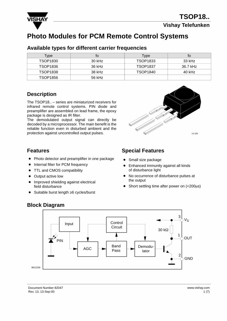
TSOP18..Vishay Telefunken
1 (7)Rev. 13, 13-Sep-00www.vishay.comDocument Number 82047
Photo Modules for PCM Remote Control Systems
Available types for different carrier frequencies Type fo Type fo
TSOP1830 30 kHz TSOP1833 33 kHz
TSOP1836 36 kHz TSOP1837 36.7 kHz
TSOP1838 38 kHz TSOP1840 40 kHz
TSOP1856 56 kHz
DescriptionThe TSOP18.. – series are miniaturized receivers forinfrared remote control systems. PIN diode andpreamplifier are assembled on lead frame, the epoxypackage is designed as IR filter. The demodulated output signal can directly bedecoded by a microprocessor. The main benefit is thereliable function even in disturbed ambient and theprotection against uncontrolled output pulses. 14 500
Features Photo detector and preamplifier in one package
Internal filter for PCM frequency
TTL and CMOS compatibility
Output active low
Improved shielding against electrical field disturbance
Suitable burst length ≥6 cycles/burst
Special Features
Small size package
Enhanced immunity against all kinds of disturbance light
No occurrence of disturbance pulses at the output
Short settling time after power on (<200s)
Block Diagram
9612226
PIN
Input
AGC
ControlCircuit
BandPass
Demodu-lator
30 k
2
3
1
VS
OUT
GND
TSOP18..Vishay Telefunken
Rev. 13, 13-Sep-00www.vishay.com Document Number 820472 (7)
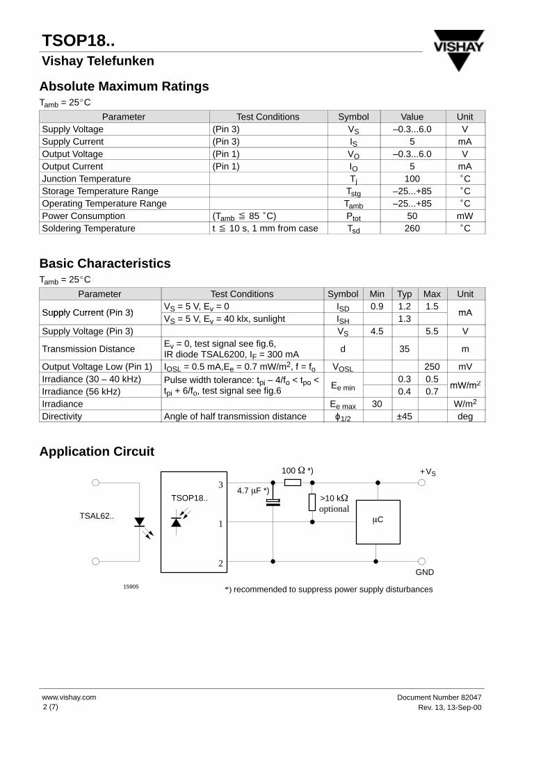
Absolute Maximum RatingsTamb = 25C
Parameter Test Conditions Symbol Value UnitSupply Voltage (Pin 3) VS –0.3...6.0 VSupply Current (Pin 3) IS 5 mAOutput Voltage (Pin 1) VO –0.3...6.0 VOutput Current (Pin 1) IO 5 mAJunction Temperature Tj 100 CStorage Temperature Range Tstg –25...+85 COperating Temperature Range Tamb –25...+85 CPower Consumption (Tamb 85 C) Ptot 50 mWSoldering Temperature t 10 s, 1 mm from case Tsd 260 C
Basic CharacteristicsTamb = 25C
Parameter Test Conditions Symbol Min Typ Max Unit
Supply Current (Pin 3)VS = 5 V, Ev = 0 ISD 0.9 1.2 1.5
mASupply Current (Pin 3)VS = 5 V, Ev = 40 klx, sunlight ISH 1.3
mA
Supply Voltage (Pin 3) VS 4.5 5.5 V
Transmission Distance Ev = 0, test signal see fig.6, IR diode TSAL6200, IF = 300 mA
d 35 m
Output Voltage Low (Pin 1) IOSL = 0.5 mA,Ee = 0.7 mW/m2, f = fo VOSL 250 mVIrradiance (30 – 40 kHz) Pulse width tolerance: tpi – 4/fo < tpo <
E0.3 0.5
mW/m2Irradiance (56 kHz)
i o otpi + 6/fo, test signal see fig.6
Ee min 0.4 0.7mW/m2
Irradiance Ee max 30 W/m2
Directivity Angle of half transmission distance ϕ1/2 ±45 deg
Application Circuit
15905
TSAL62..
TSOP18..
3
1
2
4.7 F *)
C
>10 koptional
100 *) +VS
*) recommended to suppress power supply disturbances
GND

TSOP18..Vishay Telefunken
3 (7)Rev. 13, 13-Sep-00www.vishay.comDocument Number 82047
Suitable Data FormatThe circuit of the TSOP18.. is designed in that way thatunexpected output pulses due to noise or disturbancesignals are avoided. A bandpassfilter, an integratorstage and an automatic gain control are used tosuppress such disturbances. The distinguishing mark between data signal ( notsuppressed) and disturbance signal (supressed) arecarrier frequency, burst length and Signal Gap Time(see diagram below).
The data signal should fullfill the following condition:
• Carrier frequency should be close to center fre-quency of the bandpass (e.g. 38kHz).
• Burst length should be 6 cycles/burst or longer.
• After each burst a gap time of at least 9 cycles isneccessary.
• The data format should not make a continuoussignal transmission. There must be a Signal Gap Time(longer than 15ms) at least each 90ms (see Figure A).
Some examples for suitable data format are:NEC Code (repetitive pulse), NEC Code (repetitivedata), Toshiba Micom Format, Sharp Code, RC5Code, RECS–80 Code, R–2000 Code.
When a disturbance signal is applied to the TSOP18..it can still receive the data signal. However thesensitivity is reduced to that level that no unexpectedpulses will occure.
Some examples for such disturbance signals whichare suppressed by the TSOP18.. are:
• DC light (e.g. from tungsten bulb or sunlight),
• Continuous signal at 38kHz or at any otherfrequency,
• Signals from fluorescent lamps (see Figure B).
• Continuous IR signal (e.g. 1ms burst, 2ms pause)
0 10 20 30 40 50 60 70 80 90 100
time [ms]
Signal Gap Time
Figure A: Data Signal (Output of IR Receiver) with a Signal Gap Time of 20ms
0 2 4 6 8 10 12 14 16 18 20
time [ms]
Signal Gap Time
Figure B: Disturbance Signal from Fluorescent Lamp with Signal Gap Time of 7ms

TSOP18..Vishay Telefunken
Rev. 13, 13-Sep-00www.vishay.com Document Number 820474 (7)
Typical Characteristics (Tamb = 25C unless otherwise specified)
0.7 0.8 0.9 1.0 1.1
E
/
E
– R
el. R
espo
nsiti
vity
e
min
f / f 0 – Relative Frequency
1.3
94 9102
0.0
0.2
0.4
0.6
0.8
1.0
e
1.2
f = f05%f ( 3dB ) = f0/7
Figure 1. Frequency Dependence of Responsivity
0
0.5
1.0
1.5
2.0
2.5
3.0
3.5
4.0
4.5
0.01 0.10 1.00 10.00 100.00
E – DC Irradiance (W/m2)96 12214
e m
inE
–
Thr
esho
ld I
rrad
ianc
e (m
W/m
)
2 Correlation with ambient light sources(Disturbance effect ) :10W/m21.4klx(Stand.illum.A,T=2855 K)8.2klx
(Daylight,T=5900 K)
Ambient, = 950 nm
Figure 2. Sensitivity in Bright Ambient
0.0 0.4 0.8 1.2 1.60.0
0.4
0.8
1.2
2.0
E – Field Strength of Disturbance ( kV /m )
2.0
94 8147
1.6
E
–
Thr
esho
ld Ir
radi
ance
( m
W/m
)
e m
in2
f (E )= f0
Figure 3. Sensitivity vs. Electric Field Disturbances
0.1
1.0
10.0
100.0
0.1 1.0 10.0 100.0 1000.0
Vs RMS – AC Voltage on DC Supply Voltage (mV)96 12215
e m
inE
–
Thr
esho
ld I
rrad
ianc
e (m
W/m
)
2
f = fo
10 kHz
1 kHz
100 Hz
Figure 4. Sensitivity vs. Supply Voltage Disturbances
0
0.1
0.2
0.3
0.4
0.5
0.6
0.7
0.8
0.9
1.0
4.5 4.6 4.7 4.8 4.9 5.0 5.1 5.2 5.3 5.4 5.5
VS – Supply Voltage ( V )14312
e m
inE
–
Thr
esho
ld I
rrad
ianc
e (m
W/m
)
2
Sensitivity in dark ambient
Figure 5. Sensitivity vs. Supply Voltage
Ee
t
VO
VOH
VOLt
600 s 600 s
Trep=100 ms
Ton Toff
9612218
Optical Test Signal
Output Signal, ( see Fig.7 )
TD*
* Trep–TD > 15 ms is recommended for optimal function
Figure 6. Output Function
TSOP18..Vishay Telefunken
5 (7)Rev. 13, 13-Sep-00www.vishay.comDocument Number 82047
0.4
0.45
0.50
0.55
0.60
0.65
0.70
0.75
0.80
0.1 1.0 10.0 100.0 1000.0 10000.0100000.0
Ee – Irradiance (mW/m2)16163
on
off
T
,T
–
Out
put P
ulse
Len
gth
(ms)
Ton
optical test signal, fig.6
Toff
Figure 7.
0
0.2
0.4
0.6
0.8
1.0
1.2
1.4
1.6
1.8
2.0
–30 –15 0 15 30 45 60 75 90
Tamb – Ambient Temperature ( °C )14315
I –
Sup
ply
Cur
rent
( m
A )
s
Vs = 5 V
Figure 8. Supply Current vs. Ambient Temperature
0
0.1
0.2
0.3
0.4
0.5
0.6
0.7
0.8
0.9
1.0
–30 –15 0 15 30 45 60 75 90
Tamb – Ambient Temperature ( °C )96 12221
e m
inE
–
Thr
esho
ld I
rrad
ianc
e (m
W/m
)
2
Sensitivity in dark ambient
Figure 9. Sensitivity vs. Ambient Temperature
0.5
0.6
0.7
0.8
0.9
1.0
1.1
1.2
1.3
1.4
1.5
1.6
1.7
4.5 4.6 4.7 4.8 4.9 5.0 5.1 5.2 5.3 5.4 5.5
VS – Supply Voltage ( V )14317
I –
Sup
ply
Cur
rent
( m
A )
s
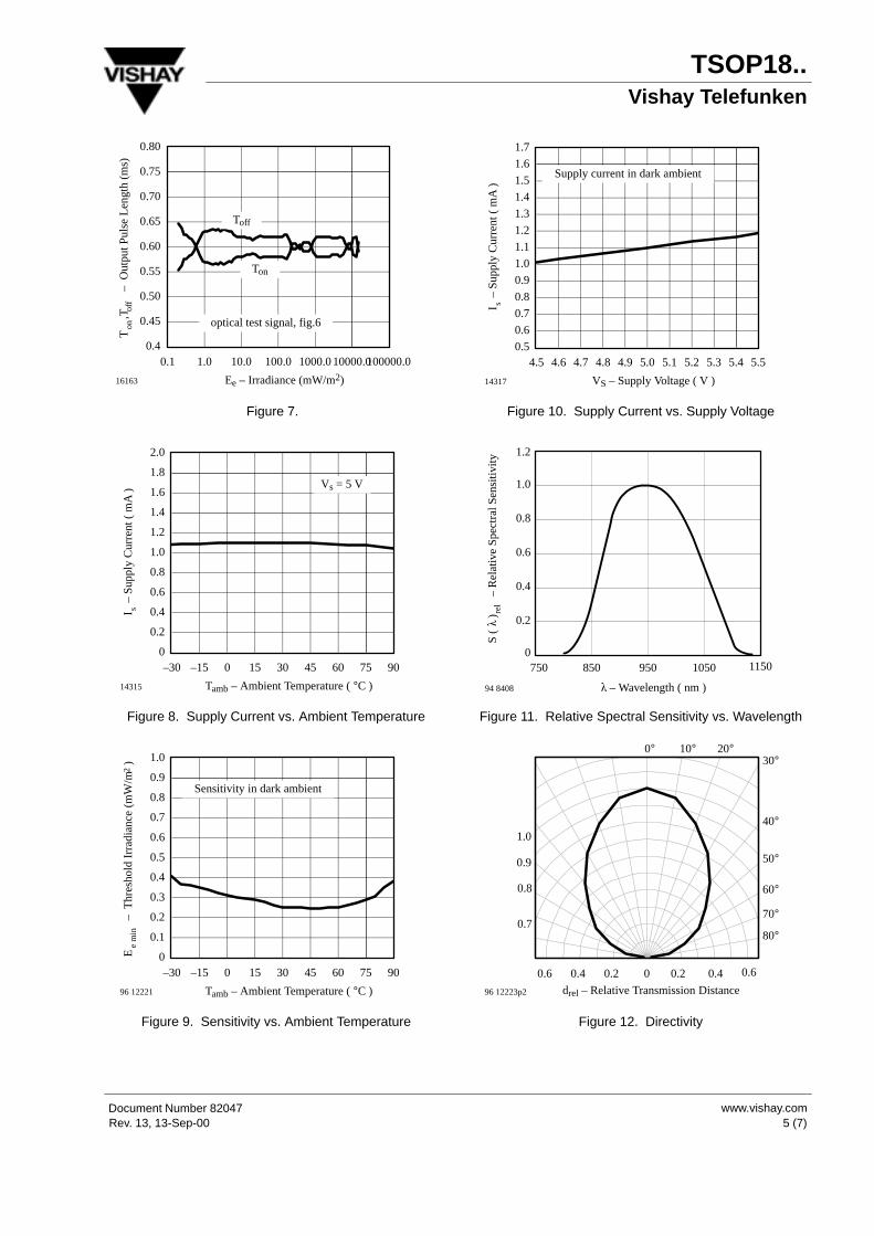
Supply current in dark ambient
Figure 10. Supply Current vs. Supply Voltage
750 850 950 10500
0.2
0.4
0.6
0.8
1.2
S (
)
– R
elat
ive
Spe
ctra
l Sen
sitiv
ityre
l
– Wavelength ( nm )
1150
94 8408
1.0
Figure 11. Relative Spectral Sensitivity vs. Wavelength
96 12223p2
0.4 0.2 0 0.2 0.4 0.60.6
0.9
0°30°
10° 20°
40°
50°
60°
70°
80°
1.0
0.8
0.7
drel – Relative Transmission Distance
Figure 12. Directivity

TSOP18..Vishay Telefunken
Rev. 13, 13-Sep-00www.vishay.com Document Number 820476 (7)
Dimensions in mm
9612211

TSOP18..Vishay Telefunken
7 (7)Rev. 13, 13-Sep-00www.vishay.comDocument Number 82047
Ozone Depleting Substances Policy Statement
It is the policy of Vishay Semiconductor GmbH to
1. Meet all present and future national and international statutory requirements.
2. Regularly and continuously improve the performance of our products, processes, distribution and operating systems with respect to their impact on the health and safety of our employees and the public, as well as their
impact on the environment.
It is particular concern to control or eliminate releases of those substances into the atmosphere which are known asozone depleting substances (ODSs).
The Montreal Protocol (1987) and its London Amendments (1990) intend to severely restrict the use of ODSs andforbid their use within the next ten years. Various national and international initiatives are pressing for an earlier banon these substances.
Vishay Semiconductor GmbH has been able to use its policy of continuous improvements to eliminate the use ofODSs listed in the following documents.
1. Annex A, B and list of transitional substances of the Montreal Protocol and the London Amendments respectively
2. Class I and II ozone depleting substances in the Clean Air Act Amendments of 1990 by the EnvironmentalProtection Agency (EPA) in the USA
3. Council Decision 88/540/EEC and 91/690/EEC Annex A, B and C ( transitional substances) respectively.
Vishay Semiconductor GmbH can certify that our semiconductors are not manufactured with ozone depletingsubstances and do not contain such substances.
We reserve the right to make changes to improve technical design and may do so without further notice.Parameters can vary in different applications. All operating parameters must be validated for each customer applicationby the customer. Should the buyer use Vishay-Telefunken products for any unintended or unauthorized application, the
buyer shall indemnify Vishay-Telefunken against all claims, costs, damages, and expenses, arising out of, directly orindirectly, any claim of personal damage, injury or death associated with such unintended or unauthorized use.
Vishay Semiconductor GmbH, P.O.B. 3535, D-74025 Heilbronn, GermanyTelephone: 49 (0)7131 67 2831, Fax number: 49 (0)7131 67 2423


