on-wafer testing of circuits through 220 ghz - nasa testing of circuits through 220 ghz ......
TRANSCRIPT
On-Wafer Testing of Circuits Through 220 GHz
Todd Gaier
Lo(ene Samoska
Jet Propulsion Laboratory, California Institute of TechnologyCharles Oleson
Oleson Microwave Labs
Greg Boll
GGB Industries
Abstract: We have jointly developed the capability to perform on-wafer s-parameter _md
noise figure measurements through 220 GHz. S-parameter test sets have been developed
covering full waveguide bands of 90-140 GHz (WR-08) and 140-220 GHz (WR-05). The
test sets have been integrated with coplanar probes to allow accurate measurements on-
wafer. We present the design and performance of the test sets and wafer probes. We also
present calibration data as well as measurements of active circuits at frequencies as high
as 215 GHz.
Introduction
Applications for frequencies higher than 100 GHz have been limited to radio-astronomy
and earth remote sensing. Improvements in semiconductor technologies have pushed
active circuits to frequencies higher than 100 GHz. Potential applications for these high
frequencies include communications, radar, passive imaging and high speed digital
networks. In order to realize the potential commercial applications for these circuits, test
equipment must be developed which can characterize these circuits in a rapid cost-
effective manner. Network analyzers are currently available spanning the continuous
frequency range 0.1-110 GHz. We present the results of three separate development
efforts which, when combined, allow for on-wafer characterization at frequencies up to
220 GHz.
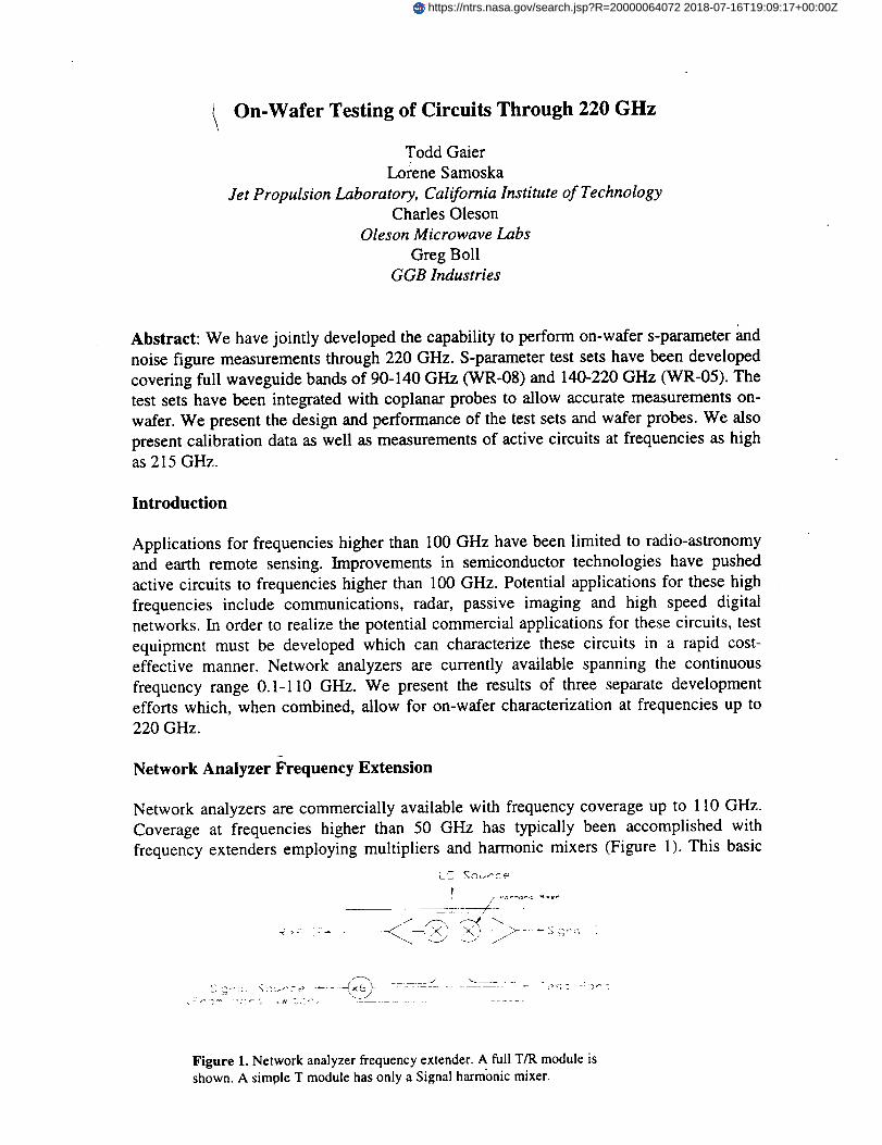
Network Analyzer Frequency Extension
Network analyzers are commercially available with frequency coverage up to 110 GHz.
Coverage at frequencies higher than 50 GHz has typically been accomplished with
frequency extenders employing multipliers and harmonic mixers (Figure 1). This basic
L_ So_'_. _
l
Figure 1. Network analyzer frequency extender. A full T/R module isshown. A simple T module has only a Signal harmonic mixer.
https://ntrs.nasa.gov/search.jsp?R=20000064072 2018-07-16T19:09:17+00:00Z
conceptis readilyextendableto frequenciesashigh as220 GHz,andpossiblyashighas325GHz. Millimeter-wave testsetscanbe readilyadaptedfor usewith network analysisequipmentfrom Hewlett-Packard(HP) and Anritsu, taking advantageof the familiarinterfacesusedindustry-wide.
Suchmillimeter-wavetest sets,or frequencyextensionmodules,must be useablewith readily availablevectornetwork analysisequipment.The following designcriteriawereestablished.1) The configurationof the frequencyextensionmodulesmust followacceptedindustrypracticeandbeableto yield S11and$21 informationin a minimal testsystemand all four "S" parametersin a completesystem.2) The IF frequencyto beutilized mustbecompatiblewith themostcommonopen-architectureanalyzersfrom HPand Anritsu. 3) The signal radio frequency (RF) and local oscillator (LO) driverequirementsmustchosenwith costacknowledgedasa majordesignrestraint.
To accomplish meaningful S-parametermeasurementsa combination of two"T/R" modulesor one "T/R" moduleand a "T" modulearerequired.The "T/R" moduleis capable of generatinga coherenttest signal and developingtwo down convertedmeasurementsignals.The downconvertedsignalsincludea referencesignal (A1) whichis a simile of the stimulussignal,and aresponsesignal(B1) whichcontainsinformationdescribing the device under test (DUT). This module can be used to measureTransmission(T) $21 characteristicsor Reflection(R) S11characteristicsof theDUT. A"T" module consistsof a single down converterfor receiving the "T/R" module testsignalasmodifiedby theDUT (B2) to measuretheTransmission(T) $21 characteristicsof theDUT. The useof two "T/R" modulesallowsthesimultaneousmeasurementof S11and$21 in theforwarddirectionandS12and$22in thereversedirection.
The down converter IF frequencyrange is 10 MHz to 300 MHz. The exactfrequencyis determinedby the analyzer.The LO drive frequencyrange is normallylimited to 20 GHz to limit that synthesizer'scost.The RF drive frequencyrangeusedisas high as possible and is limited only by the available frequencyrange of othercomponentsin the "T/R" module.The test signal is producedby a two-stagemultiplierchain,with eachstagedriveninto saturationto producetheflattestandmoststablesignal.The test signal is appliedto a directionalcouplerthroughan isolator to providea goodsourcematchfor themeasurement.
TheRF drive is fedto only one"T/R" moduleat atime in thecaseof atwo "T/R'"modulesystem.By virtueof thesignalpathchosen,forwardor reverse,thetestconvertersdevelopeither S11and $21 or $22 andS12.Thetest converterin themodulecontainingthe "active" signal sourceproducesthe reflection signal and the test converterin theinactivemoduleproducesthetransmissionsignal.TheLO drive is "split" andprovidedtoall of themodulesin anygiventest setconfiguration.In the "T/R" module,theLO signalis "split" againandfed to bothdownconverters.TheLO is thencoherentat anyconverterwith respect to any other converter. The total system becomescoherent throughcomparisonof any of the test convertersignal to the "active" referenceconvertersignalenabling phaseand amplitude information to be obtained.Thesedownconvertersaremadeup of balancedharmonicmixers and low noiseI.F. amplifiers.The LO harmonicusedfor the conversionprocessis alwaysthe highestuseablefor the bandof interestwithin the20GHz LO limitation.

The dynamic rangeof thesemodulesvarieswith the desiredwaveguidebandofoperation.The dynamic rangeachievedfor the 90 to 140 GHz band is typically betterthan 80 dB. The correctedsourcematch is typically 35 to 40 dB and the correcteddirectivity is typically 45 to 50dB enablingreflectionmeasurementsto better than60dB(Figure2). A 150-220GHz test setusing "T/R" and "T" modulesexhibits greaterthan
:'glq_l_T"3_
Figure 2a. Calibrated dynamic range of throughmeasurement, 85-140 GHz.
Figure 2b. Calibrated dynamic range for reflectionmeasurements, 85-140 GHz.
50 dB (Figure 3) dynamic range for through measurements and a minimum of 25 dB for
reflection measurements, although full calibration will yield even greater dynamic range.
The test signal power ranges from -10 to +3 dBm, which may exceed the input
>1111/141 Io8
11.o
¥
A REF-:EFI_._C:E PALLE
i: I --_ 4, I] dB
irTA_r l_o,llllllloo o_1iii11 ill, IIIIIHII
1
r_
A "-
¥ 4
iT_r 11o•1tlltlltl o_mrio, olllllllo o_m
I-%'I:lI,*'_
i
Irg:g,'=
Figure 3a. Dynamic range of through measurement,
uncalibrated, 150-220 GHz.
Figure 3b. Uncalibrated one-port response of waveguide
termination, short reference, 150-220 GHz.
level handling capability the DUT being tested. When this problem is foreseen, provision
can be made for attenuating the test signal power• The IF output level of the
downconverters may exceed the calibrated input power capability of the analyzer. In that
case the particular IF causing the overload can be attenuated to an acceptable level. The
design of these modules allows operation for prolonged periods of time in a laboratory
environment• Several systems of WR-08 have been delivered and multiple WR-05

systemswill be in operationshortly. A WR-06 designhasbeencompletedand designefforts are underway for WR-04 and WR-03. The lack of commercially availablewaveguidecomponentscurrentlylimits theseefforts to WR-03, i.e.,325GHz
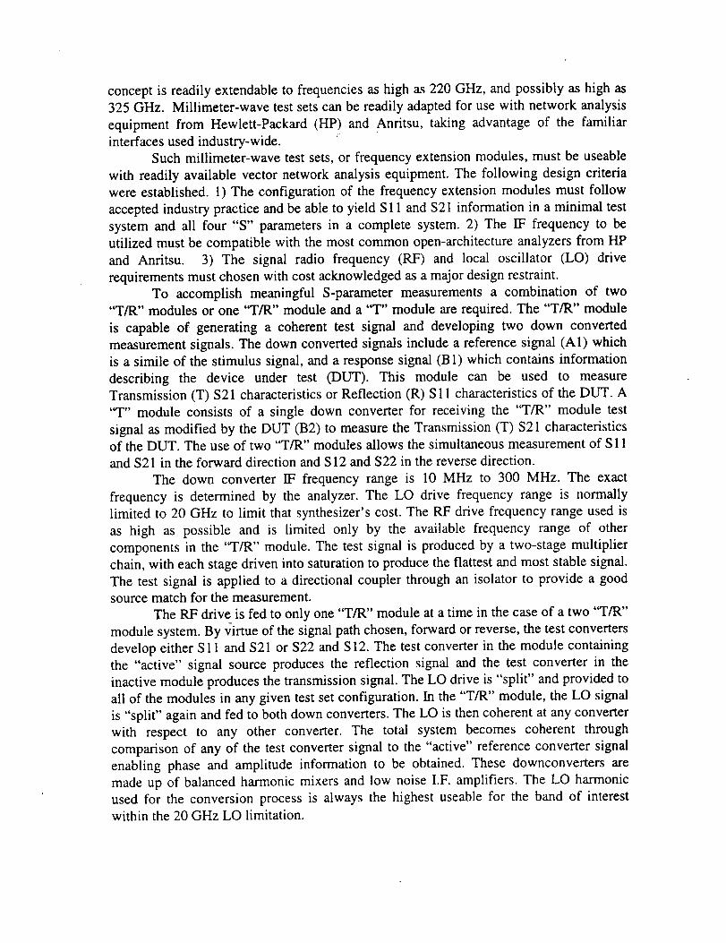
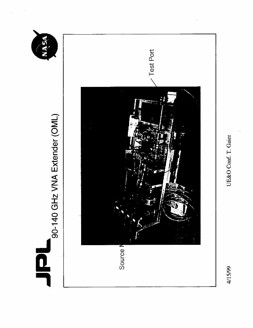
Millimeter-wave Wafer Probes
Circuit measurements at frequencies above 100 GHz have required packaging of circuits
into waveguide blocks. This technique is slow and cumbersome, and often does not yield
true circuit performance. Commercialization of high frequency circuits requires high
volume low-cost characterization of circuits.
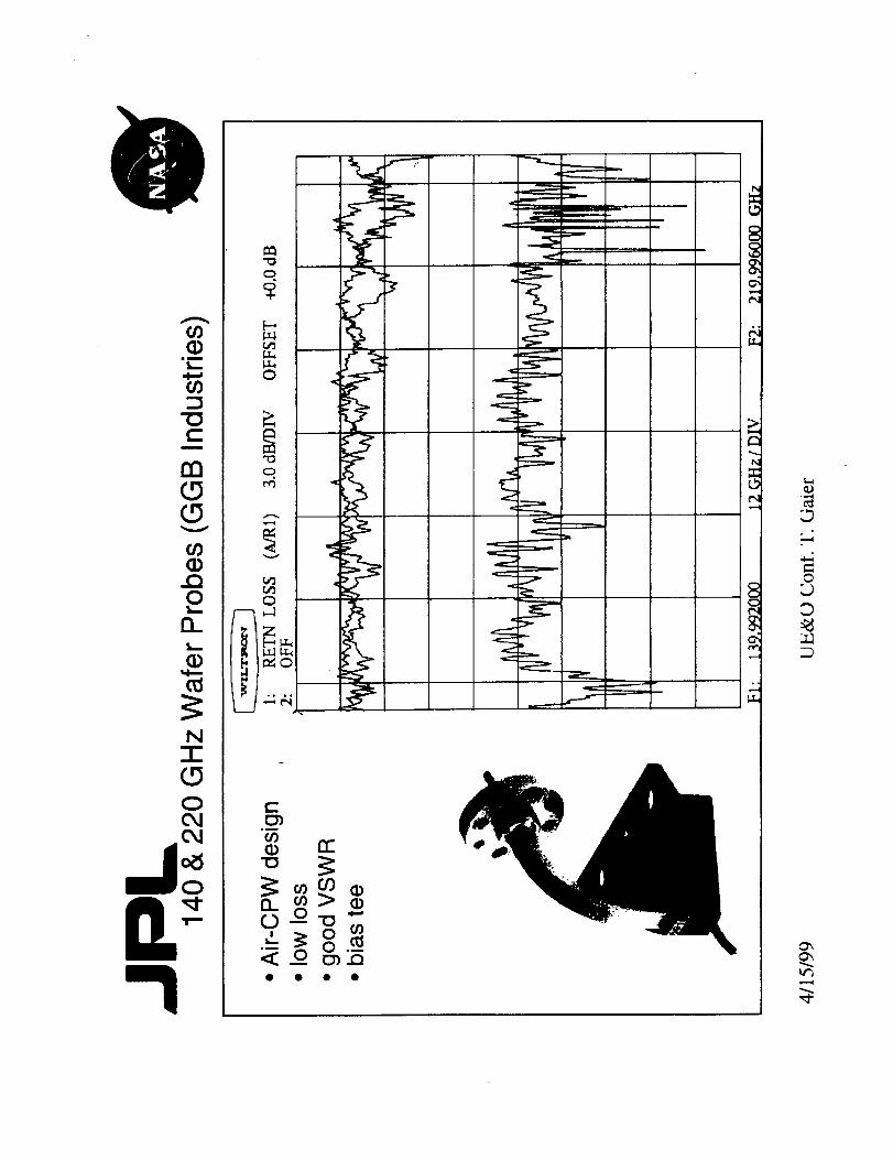
A line of co-planar probes for on-wafer testing of sub-millimeter circuits has been
developed by GGB Industries, Inc., and sold under the Picoprobe trademark. The 220
GHz probe shown in Figure 4, has a short coaxial probe body coupled to a WR-5
waveguide section for connection to test instruments. In common with all Picoprobe
microwave probes, the probe tips are individually spring-loaded Beryllium-Copper for
making reliable connection even to non-planar structures. The design is readily
I: RETN LOSS (/_RI) 3.0 dlB/DI_' OFFSET 40.0 dBOFF
^_. ,{_,AA ._,._ ._)n._,. _.,
'V " Vf
Ft: 1.39.992000 1.2 Gl-lz ¢ DIV F2: 21.9.996000 GRz
Figure 4. Photoof 220 GHz
wafer probe
Figure 5. One-port performance of 220 GHz probe.The two top traces show open and short, while thebottom shows a load.
extendable to 300 GHz and above. A bias T is included to provide current (up to 1.5A) to
the circuit under test and includes loss elements to absorb signals below the WR-5 cutoff
frequency (115 GHz) where the waveguide becomes highly reflective. A special
miniaturized co-planar calibration substrate (CS-15) has been developed for SOLT, LRL,and LRM calibrations which is based on 25 micron wide signal lines and 25 x 25 micron
probe pads.
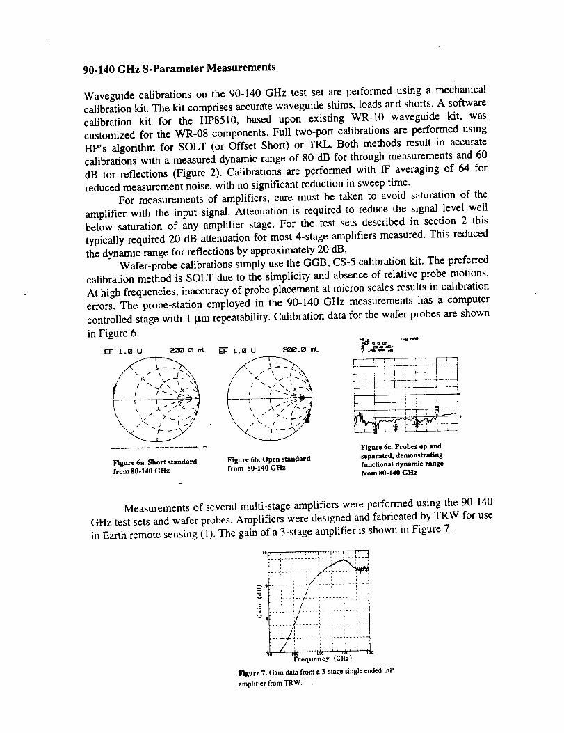
The one-port performance of the 220 GHz probe, Figure 5, shows the reflection
from a short and an open (top two traces) and that from a 50 Ohm load (bottom trace).
The approximately 4dB two-way loss for the short and open indicates a one-way loss of
about 2dB. The raggedness results from the limited dynamic range of the custom built
scalar network analyzer assembled at GGB Industries, Inc., for use in the development of
this probe.
90-140 GHz S-Parameter Measurements
Waveguide calibrations on the 90-140 GHz test set are performed using a mechanical
calibration kit. The kit comprises accurate waveguide shims, loads and shorts. A software
calibration kit for the HP8510, based upon existing WR-10 waveguide kit, was
customized for the WR-08 components. Full two-port calibrations are performed using
HP's algorithm for SOLT (or Offset Short) or TRL. Both methods result in accuratecalibrations with a measured dynamic range of 80 dB for through measurements and 60
dB for reflections (Figure 2). Calibrations are performed with IF averaging of 64 for
reduced measurement noise, with no significant reduction in sweep time.
For measurements of amplifiers, care must be taken to avoid saturation of the
amplifier with the input signal. Attenuation is required to reduce the signal level well
below saturation of any amplifier stage. For the test sets described in section 2 this
typically required 20 dB attenuation for most 4-stage amplifiers measured. This reduced
the dynamic range for reflections by approximately 20 dB.
Wafer-probe calibrations simply use the GGB, CS-5 calibration kit. The preferred
calibration method is SOLT due to the simplicity and absence of relative probe motions.
At high frequencies, inaccuracy of probe placement at micron scales results in calibration
errors. The probe-station employed in the 90-140 GHz measurements has a computer
controlled stage with 1 l.tm repeatability. Calibration data for the wafer probes are shown
in Figure 6.
Figure 6a. Short standardfrom 80-140 GHz
_.0 u _._ mL
Figure 6b. Open standardfrom 80-140 GHz
1 i _ ; I I r--_
Figure 6c. Probes up and
separated, demonstratingfunctional dynamic range
from 80-140 GHz
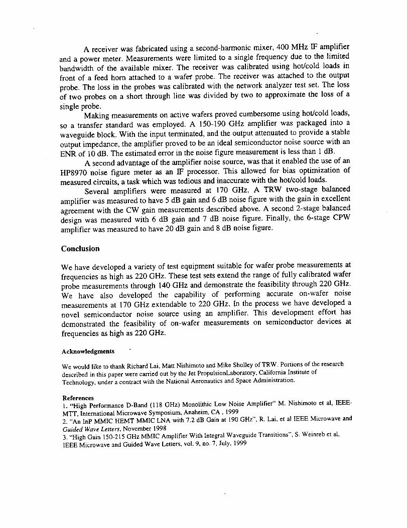
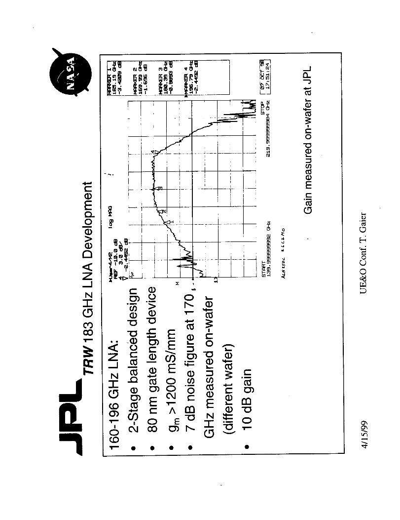
Measurements of several multi-stage amplifiers were performed using the 90-140
GHz test sets and wafer probes. Amplifiers were designed and fabricated by TRW for use
in Earth remote sensing (1). The gain of a 3-stage amplifier is shown in Figure 7.
.... I .... l .... : .... I .... i*" 1" l ''_.__,___,.._._._.-.-.---,---,--
.....i:ii !:iiii!!iiiiFrequency (GDIz)
Figure 7. Gain data from a 3-stage single ended haP
amplifier from TRW.
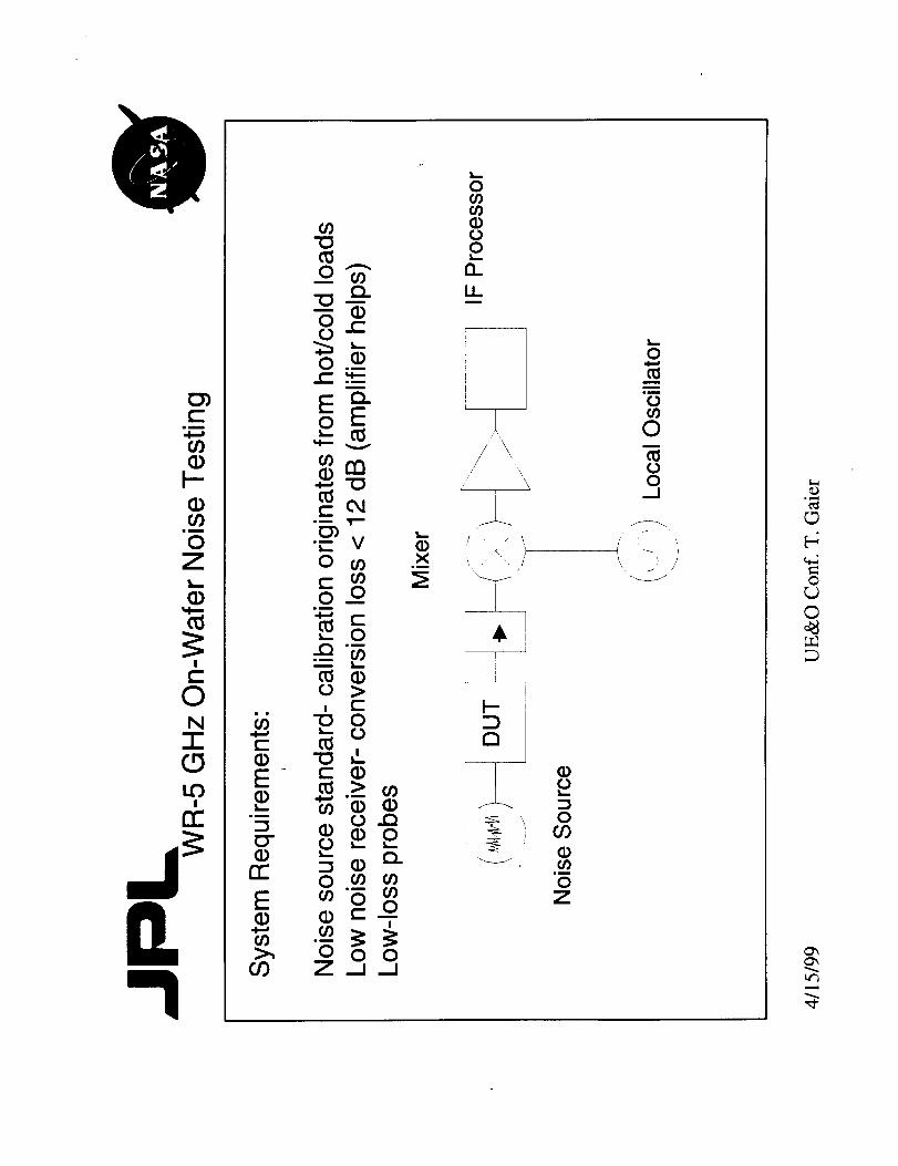
A receiver was fabricated using a second-harmonic mixer, 400 MHz IF amplifier
and a power meter. Measurements were limited to a single frequency due to the limitedbandwidth of the available mixer. The receiver was calibrated using hot/cold loads in
front of a feed horn attached to a wafer probe. The receiver was attached to the output
probe. The loss in the probes was calibrated with the network analyzer test set. The loss
of two probes on a short through line was divided by two to approximate the loss of a
single probe.
Making measurements on active wafers proved cumbersome using hot/cold loads,
so a transfer standard was employed. A 150-190 GHz amplifier was packaged into a
waveguide block. With the input terminated, and the output attenuated to provide a stable
output impedance, the amplifier proved to be an ideal semiconductor noise source with an
ENR of 10 dB. The estimated error in the noise figure measurement is less than 1 dB.
A second advantage of the amplifier noise source, was that it enabled the use of an
HP8970 noise figure meter as an IF processor. This allowed for bias optimization of
measured circuits, a task which was tedious and inaccurate with the hot/cold loads.
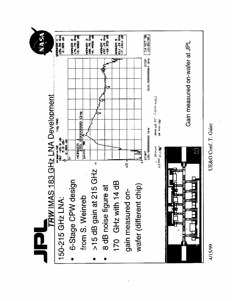
Several amplifiers were measured at 170 GHz. A TRW two-stage balanced
amplifier was measured to have 5 dB gain and 6 dB noise figure with the gain in excellent
agreement with the CW gain measurements described above. A second 2-stage balanced
design was measured with 6 dB gain and 7 dB noise figure. Finally, the 6-stage CPW
amplifier was measured to have 20 dB gain and 8 dB noise figure.
Conclusion
We have developed a variety of test equipment suitable for wafer probe measurements at
frequencies as high as 220 GHz. These test sets extend the range of fully calibrated wafer
probe measurements through 140 GHz and demonstrate the feasibility through 220 GHz.
We have also developed the capability of performing accurate on-wafer noise
measurements at 170 GHz ,extendable to 220 GHz. In the process we have developed a
novel semiconductor noise source using an amplifier. This development effort has
demonstrated the feasibility of on-wafer measurements on semiconductor devices at
frequencies as high as 220 GHz.
Acknowledgments -
We would like to thank Richard Lai, Matt Nishimoto and Mike Sholley of TRW. Portions of the research
described in this paper were carried out by the Jet PropulsionLaboratory, California Institute of
Technology, under a contract with the National Aeronautics and Space Administration.
References1. "High Performance D-Band (118 GHz) Monolithic Low Noise Amplifier" M. Nishimoto et al, IEEE-
MTr, International Microwave Symposium, Anaheim, CA, 19992. "An InP MMIC HEMT MMIC LNA with 7.2 dB Gain at 190 GHz", R. Lai, et al IEEE Microwave and
Guided Wave Letters, November 1998
3. "High Gain 150-215 GHz MMIC Amplifier With Integral Waveguide Transitions", S. Weinreb et al,IEEE Microwave and Guided Wave Letters, vol. 9, no. 7, July, 1999

N
0
0
©

e-
oe-
"I
0_
o
0

Z
!
r_
0
©
t¢3
0V
c-
XW
<Z>N
0
!
0
0co
00_
(I)
°_
0L_©
LQ
N
O
O

CD
,4row
=QOlib
0_
CD
N
0
,Tn!
_s
[L
1in
c_mmmm im
LL.-n
c_
OCJ
©
L_
Lt_

-,i
._o
_ _ o_. _ ,.,_
o_,_
0
©
_r_
0m
a
z
Q_
c-O
._
0
©
4.u
!
0
EC
o
©
Cmm
I'-CD
im
0Z
c
o
.Iii
-a
-oo-m0 _...-0
_o.__
0
00
o_LL
8
0cDm ',,
•r- v _0 m .x
o_O
_._ ,I
_ _o
_ _-_
1
a
0
0
0Z
r_
0
r..)
©