on the ground state and evolution of structural and
TRANSCRIPT
Clemson UniversityTigerPrints
All Dissertations Dissertations
12-2017
On the Ground State and Evolution of Structuraland Transport Properties of Tin SelenideYufei Liu
Follow this and additional works at: https://tigerprints.clemson.edu/all_dissertations
Part of the Physics Commons

On the Ground State and Evolution of Structural andTransport Properties of Tin Selenide
A Dissertation
Presented to
the Graduate School of
Clemson University
In Partial Fulfillment
of the Requirements for the Degree
Doctor of Philosophy
General Physics
by
Yufei Liu
December 2017
Accepted by:
Dr. Jian He, Committee Chair
Dr. Murray Daw
Dr. Apparao Rao
Dr. Sumanta Tewari

Abstract
The recent surge of interest in tin selenide (SnSe) is due to the reported record-high ther-
moelectric figure of merit at elevated temperatures. While the researchers are exerting tremendous
efforts to further improve the thermoelectric performance of SnSe via doping and nanostructuring, it
is getting more and more apparent that SnSe is fascinating in many aspects of fundamental physics.
SnSe is, in many aspects, an outlier of the current materials selection rules for high thermoelec-
tric performance. Hence, answering why thermoelectric performance is high in SnSe should come
before addressing how to further improve its thermoelectric performance. To this end, there are
three primary questions worth immediate attention, one related to the thermal nature of SnSe: (i)
why the lattice thermal conductivity is low in such a simple-structured light element containing
binary compound; and the other two related to the electrical nature of SnSe: what is the electronic
ground state of this material. The second question can be addressed by answering to sub-questions:
(ii) what is the origin of the resistivity anomaly around 50 K; and (iii) what is the nature of the
metal-insulator transition driven by Sn deficiency.
In this thesis, we intend to address the three questions by means of the temperature depen-
dent resistivity, Seebeck coefficient, Hall coefficient, specific heat, thermal conductivity, magnetic
susceptibility and X-ray diffraction measurements in conjunction with density functional theory cal-
culations. These results presented a grand picture how SnSe evolves structurally, electrically, and
thermally from a low temperature metallic state to a high temperature semiconducting state toward
a promising thermoelectric performance. In particular, we found that (i) high quality pristine SnSe
single crystals exhibit a metallic ground state (that is, a small but robust Fermi surface with mul-
tiple pockets) with a coexisting band gap; (ii) off-stoichiometry and doping could destabilize the
metallic state; (iii) the low-lying optical phonon modes and strong anharmonicity contribute to the
low lattice thermal conductivity. We obtained a thermoelectric figure of merit ZT ∼ 1.0, ∼ 0.8 and
ii

∼ 0.25 at 850 K along the b, c and a directions in high quality single crystalline SnSe. We have also
discussed the formation of the Fermi surface in relation to Sn vacancies and the disorder induced
metal-to-insulator transition in light of Anderson localization.
iii

Acknowledgments
Firstly, I want to thank my PhD adviser, Dr. Jian He. He is both my mentor and friend.
During my PhD years, he has taught me so much in not only physics, but also life.
Another person that helped me a lot is Dr. Pai-Chun Wei at Institute of Physics, Academia
Sinica, Taiwan. As an expert in crystal growth, he has prepared high quality tin selenide single
crystals in this project. More importantly, through many inspiring discussions with Dr. Jian He
and Dr. Paichun Wei, I am thinking and acting more and more like a scientist, and this is what a
physics PhD thesis is about.
Also, I would like to thank Drs. Chen-Rong Hsing, Tsu-Ling Hung, Ching-Ming Wei,
and Yang-Yuan Chen at Academia Sinica, Taiwan; Mr. Xuewang Wu, Prof. Xiaojia Wang at
University of Minnesota; Changlong Li, Prof. Kyle Brinkman, Yongchang Dong, Fengjiao Liu,
Fanchen Meng, Dr. Don Liebenberg, Prof. Apparao Rao, Prof. Murray Daw, Prof. Sumanta
Tewari, Prof. Terry Tritt at Clemson University; Dr. Nao Cai, Prof. Baosheng Li at SUNY,
Stony Brook; Dr. Raphael Hermann at Oak Ridge National Lab; Weiwu Li and Dr. Wenjie Xie
at University of Stuttgart. It would not be possible to form a thesis without their support and
assistance. Especially, Dr. Sriparna Bhattacharya and Dr. Menghan Zhou have conducted many
low temperature thermoelectric measurements.
I want to thank my group members, Fanchen Meng, Yamei Liu, and group alumni from
our group and Dr. Terry Tritt’s group, Drs. Dale Hitchcock, Menghan Zhou, Daniel Thompson,
Tim Holgate, Xiaoyu Zeng and Song Zhu. As a tradition of Dr He group, a PhD candidate must
work on 6-10 mini-projects on various topics before he/she dedicates about 2 years on a new topic
towards his/her PhD degree. My PhD thesis is no exception, which has little overlap with my
earlier work. Notably, most sample preparations and characterizations were conducted through off-
campus collaborations, as they are either beyond the on-campus resources or due to the restriction of
iv
time. Nonetheless, it is my thesis as I have independently contributed some key ideas and designed
experiments to verify or invalidate these ideas to further our understanding of SnSe.
This research is supported by NSF DMR 1307740.
v

Table of Contents
Title Page . . . . . . . . . . . . . . . . . . . . . . . . . . . . . . . . . . . . . . . . . . . . i
Abstract . . . . . . . . . . . . . . . . . . . . . . . . . . . . . . . . . . . . . . . . . . . . . ii
Acknowledgments . . . . . . . . . . . . . . . . . . . . . . . . . . . . . . . . . . . . . . . iv
List of Tables . . . . . . . . . . . . . . . . . . . . . . . . . . . . . . . . . . . . . . . . . . viii
List of Figures . . . . . . . . . . . . . . . . . . . . . . . . . . . . . . . . . . . . . . . . . . ix
1 INTRODUCTION TO THERMOELECTRICITY . . . . . . . . . . . . . . . . . . 11.1 Material Aspects of Thermoelectricity . . . . . . . . . . . . . . . . . . . . . . . . . . 21.2 A ”Flow” View of Thermoelectricity . . . . . . . . . . . . . . . . . . . . . . . . . . . 41.3 Nature of Seebeck Coefficient . . . . . . . . . . . . . . . . . . . . . . . . . . . . . . . 8
2 THERMOELECTRIC PROPERTIES OF TIN SELENIDE . . . . . . . . . . . . 162.1 Thermoelectric Properties of SnSe . . . . . . . . . . . . . . . . . . . . . . . . . . . . 162.2 Previous Works on SnSe . . . . . . . . . . . . . . . . . . . . . . . . . . . . . . . . . . 172.3 Single Crystal Growth and Crystal Structure of SnSe . . . . . . . . . . . . . . . . . 182.4 TE Properties of Single Crystalline SnSe . . . . . . . . . . . . . . . . . . . . . . . . . 21
3 LOW THERMAL CONDUCTIVITY IN TIN SELENIDE . . . . . . . . . . . . . 303.1 Mechanisms Underlying Low Thermal Conductivity . . . . . . . . . . . . . . . . . . 303.2 Thermal Conductivity of SnSe . . . . . . . . . . . . . . . . . . . . . . . . . . . . . . 393.3 Phonon Dispersion Relations of SnSe . . . . . . . . . . . . . . . . . . . . . . . . . . . 453.4 Resonant Bonding in SnSe . . . . . . . . . . . . . . . . . . . . . . . . . . . . . . . . . 50
4 ELECTRONIC STATES IN TIN SELENIDE . . . . . . . . . . . . . . . . . . . . . 564.1 Density Functional Theory (DFT) Calculations on Electronic Band Structure of SnSe 574.2 Experimental Results . . . . . . . . . . . . . . . . . . . . . . . . . . . . . . . . . . . . 584.3 Regime (iii): ∼ 600 K - ∼ 800 K . . . . . . . . . . . . . . . . . . . . . . . . . . . . . 654.4 Regime (ii): ∼ 50 K - ∼ 600 K . . . . . . . . . . . . . . . . . . . . . . . . . . . . . . 674.5 Regime (i): Below 50 K . . . . . . . . . . . . . . . . . . . . . . . . . . . . . . . . . . 704.6 Probe Localization via Doping Study . . . . . . . . . . . . . . . . . . . . . . . . . . . 78
5 CONCLUSIONS AND FUTURE WORKS . . . . . . . . . . . . . . . . . . . . . . 86
Appendices . . . . . . . . . . . . . . . . . . . . . . . . . . . . . . . . . . . . . . . . . . . 89A Onsager’s Reciprocal Relations . . . . . . . . . . . . . . . . . . . . . . . . . . . . . . 90B Brief Introduction to Pycnometer . . . . . . . . . . . . . . . . . . . . . . . . . . . . . 93C Resonant Bonding . . . . . . . . . . . . . . . . . . . . . . . . . . . . . . . . . . . . . 94D Time-Domain Thermoreflectance . . . . . . . . . . . . . . . . . . . . . . . . . . . . . 100
vi
Bibliography . . . . . . . . . . . . . . . . . . . . . . . . . . . . . . . . . . . . . . . . . . .102
vii
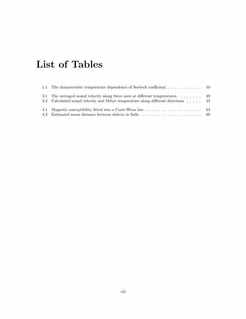
List of Tables
1.1 The characteristic temperature dependence of Seebeck coefficient. . . . . . . . . . . . 10
3.1 The averaged sound velocity along three axes at different temperatures. . . . . . . . 393.2 Calculated sound velocity and Debye temperature along different directions . . . . . 45
4.1 Magnetic susceptibility fitted into a Curie-Weiss law . . . . . . . . . . . . . . . . . . 644.2 Estimated mean distance between defects in SnSe . . . . . . . . . . . . . . . . . . . . 69
viii

List of Figures
1.1 Number of academic publications on thermoelectricity since 1998. . . . . . . . . . . . 21.2 Relationship between electrical properties and the power of carrier concentration. . . 41.3 Relationship between efficiency and heat source temperature for different ZT values. 51.4 Accuracy estimated by Goldsmid-Sharp relation versus the maximum Seebeck coeffi-
cient. . . . . . . . . . . . . . . . . . . . . . . . . . . . . . . . . . . . . . . . . . . . . . 13
2.1 Number of thermoelectric research publications for selected compounds from 1997 to2016. . . . . . . . . . . . . . . . . . . . . . . . . . . . . . . . . . . . . . . . . . . . . . 18
2.2 The lattice structure of SnSe in Pnma and Cmcm phases. . . . . . . . . . . . . . . . 192.3 Lattice parameters along three axes over a wide temperature range. . . . . . . . . . 202.4 Sn-Se binary phase diagram. . . . . . . . . . . . . . . . . . . . . . . . . . . . . . . . 212.5 Thermal neutron rocking curves and the single crystal grown by Bridgeman method. 222.6 The electrical propeties of SnSe single crystals. . . . . . . . . . . . . . . . . . . . . . 232.7 Electrical resistivity anomaly around 50 K. . . . . . . . . . . . . . . . . . . . . . . . 242.8 Thermal conductivity of SnSe single crystals. . . . . . . . . . . . . . . . . . . . . . . 262.9 Figure of merit ZT of SnSe single crystals along three directions. . . . . . . . . . . . 282.10 Temperature dependence of electrical resistivities for SnSe samples with different Sn
deficiency. . . . . . . . . . . . . . . . . . . . . . . . . . . . . . . . . . . . . . . . . . . 29
3.1 Normal process (N-process) and Umklapp process (U-process). . . . . . . . . . . . . 333.2 Calculated frequency dependence of phonon relaxation time. . . . . . . . . . . . . . . 353.3 Molar heat capacity cP of SnSe as a function of temperature. . . . . . . . . . . . . . 373.4 Estimated phonon mean free path along three primary crystallographic axes of SnSe. 403.5 Temperature dependence of volume thermal expansion coefficient. . . . . . . . . . . 423.6 Calculated phonon relaxation time and thermal conductivity due to U-process and
ph-e scattering for SnSe. . . . . . . . . . . . . . . . . . . . . . . . . . . . . . . . . . . 433.7 Comparison of Umklapp and Normal scattering rates in PbTe and SnTe at 300 K. . 443.8 Phonon dispersion relation of SnSe calculated using DFT. . . . . . . . . . . . . . . . 463.9 Calculated phonon density of states (PDOS) of SnSe at 65 K. . . . . . . . . . . . . . 473.10 (a-c) Comparison of measured and calculated specific heat at different temperature
ranges. (d) C/T vs. T 2 plot for both measured and calculated data. . . . . . . . . . 483.11 The displacement pattern for the lowest-energy TOc mode (Pnma) in SnSe. . . . . . 493.12 Illustration of how long-ranged interaction softens phonon modes. . . . . . . . . . . . 513.13 (a)Calculated temperature dependence of the bond length in SnSe, and the Sn coor-
dination polyhedron in (b) Pmna and (c) Cmcm phases, respectively. . . . . . . . . . 533.14 Crystal lattice of Bi. . . . . . . . . . . . . . . . . . . . . . . . . . . . . . . . . . . . . 54
4.1 Temperature dependence of electrical resistivity and Seebeck coefficient. . . . . . . . 574.2 Electronic band structure of SnSe at different temperatures using DFT calculations. 594.3 Projected electronic density of states in SnSe. . . . . . . . . . . . . . . . . . . . . . . 594.4 Carrier mobility of SnSe along three axes. Inset: carrier concentration. . . . . . . . . 61
ix

4.5 Sommerfeld coefficients for different elements. . . . . . . . . . . . . . . . . . . . . . . 624.6 Temperature dependence of magnetic susceptibility of SnSe single crystals. . . . . . 634.7 Magnetic moment M vs. external field H for SnSe single crystals measured at 1.8 K. 664.8 Electrical Resistivity and carrier concentration reported in 1981. . . . . . . . . . . . 684.9 Calculated Fermi surface with different Fermi energies. . . . . . . . . . . . . . . . . . 694.10 Left: Mossbauer spectroscopy of SnSe crystals in this work. Right: Mossbauer spec-
troscopy of SnSe2. . . . . . . . . . . . . . . . . . . . . . . . . . . . . . . . . . . . . . 704.11 Comparison of measured Seebeck coefficients and estimated values using the Pisarenko
relation. . . . . . . . . . . . . . . . . . . . . . . . . . . . . . . . . . . . . . . . . . . . 714.12 lnσ vs. 1/T for temperatures below 50 K. . . . . . . . . . . . . . . . . . . . . . . . . 724.13 Variable range hopping fitting for SnSe. . . . . . . . . . . . . . . . . . . . . . . . . . 734.14 Resistivity vs. Seebeck coefficient plot of SnSe. . . . . . . . . . . . . . . . . . . . . . 744.15 The categories of metal to insulator transition (MIT). . . . . . . . . . . . . . . . . . 754.16 Mott criterion diagram. . . . . . . . . . . . . . . . . . . . . . . . . . . . . . . . . . . 764.17 Schematic of the change in EF with temperature increases. . . . . . . . . . . . . . . 784.18 Temperature evolution for the ARPES-extracted effective masses of difference bands. 794.19 Electrical resistivity vs. temperature for SnSe of different stoichiometry. . . . . . . . 804.20 Left:Changes of resistivity and its temperature dependence on annealing. Right: Re-
sistivity of GeSb2Te4 films with different annealing temperature. . . . . . . . . . . . 814.21 Schematic plot of the metal-insulator transition in some phase-change materials . . . 824.22 Schematic plot of disorder induced metal-insulator transition. . . . . . . . . . . . . . 834.23 dI/dV spectroscopy of Sn vacancy in SnSe. . . . . . . . . . . . . . . . . . . . . . . . 834.24 Electrical resistivity of In-doped SnSe. . . . . . . . . . . . . . . . . . . . . . . . . . . 844.25 ln(σ) vs. T−1/4 for InxSn1−xSe samples. . . . . . . . . . . . . . . . . . . . . . . . . . 85
5.1 Group-subgroup relations associated with particular tilt systems for ABX3 singleperovskites. . . . . . . . . . . . . . . . . . . . . . . . . . . . . . . . . . . . . . . . . . 87
A1 AccuPyc II 1340 Pycnometer and the instrument schematic. . . . . . . . . . . . . . . 93A2 Lewis diagram of Cl2 and HCl. . . . . . . . . . . . . . . . . . . . . . . . . . . . . . . 94A3 Lewis diagram of nitrate polyatomic ion NO3
−. . . . . . . . . . . . . . . . . . . . . . 95A4 Lewis-like diagram of benzene. . . . . . . . . . . . . . . . . . . . . . . . . . . . . . . 95A5 Schematic diagram of resonant bonding for Sb. . . . . . . . . . . . . . . . . . . . . . 96A6 Hybridization vs. ionicity for different materials. . . . . . . . . . . . . . . . . . . . . 97A7 Normalized trace of interatomic force constant tensors versus atomic distances. . . . 99A8 Schematic diagram of experimental setup for TDTR. . . . . . . . . . . . . . . . . . . 100A9 TDTR results for SnSe single crystal. . . . . . . . . . . . . . . . . . . . . . . . . . . . 101
x

Chapter 1
INTRODUCTION TO
THERMOELECTRICITY
Tin Selenide (SnSe) is a fascinating material recently re-discovered to exhibit rich physics
and promising thermoelectric properties. The purpose of the present thesis is two-fold:
(i) by thermoelectrics: we use the electrical conductivity (the inverse of resistivity), Seebeck
coefficient (aka thermopower), and thermal conductivity in conjunction with specific heat, Hall
coefficient, magnetic susceptibility measurements and density functional theory (DFT) calculations
to probe the charge, lattice and orbital degrees of freedom and their interplay in high quality pristine
SnSe single crystals. In this thesis, the emphasis is on (i), i.e., the fundamental study of SnSe,
especially the mechanisms underlying the low thermal conductivity and the ground state of SnSe.
(ii) for thermoelectrics: the results derived from (i) are used to shed light on the origin of
high thermoelectric performance of SnSe. The performance of a thermoelectric material is gauged
by the dimensionless figure of merit, ZT , defined as ZT = σα2T/κ [1], where σ is the electrical
conductivity, α the Seebeck coefficient (i.e., thermopower), κ the thermal conductivity, and T the
temperature in Kelvin. SnSe is a seemingly simple binary compound that contains no heavy elements,
making itself an ”outlier” of the traditional material selection criteria for good thermoelectrics.
Understanding why SnSe possesses a high thermoelectric performance would open an avenue for
developing new higher performance thermoelectric materials.
In the remainder of Chapter 1, we will have a brief introduction of thermoelectric materials
1

Figure 1.1: Number of academic publications on thermoelectricity since 1998.
research and, in particular, a ”flow” view of thermoelectric process.
1.1 Material Aspects of Thermoelectricity
Thermoelectrics is an application driven material oriented topic of fundamental research
that spans the basic discipline of physics, chemistry, materials science, mechanical engineering and
electrical engineeringi [1–4]. The research on thermoelectrics is getting more and more popular over
the last two decades, as shown in Figure 1.1. Novel materials and especially the new transport
mechanisms discovered in materials are the fountain of youth for thermoelectric research. Despite
the field of thermoelectric research is application driven, it is the rich physics embodied in the
materials that drive the field forward.
Modern thermoelectric materials research was initiated in the 1950s’ and concomitant with
the development of modern semiconductor physics and quantum mechanics [5]. A good thermoelec-
tric material requires a high electrical conductivity, a low thermal conductivity, and a high Seebeck
coefficient. Over decades, the researchers have come up with a set of material selection criteria
(guidelines) for better thermoelectric materials in semiconductors. Conventionally, two basic pa-
rameters of semiconductors have been used to empirically determine the thermoelectric performance
of a material: the carrier concentration n, and the electronic band gap Eg. There are several guide-
lines. The first one states that a good thermoelectric material should be a degenerate semiconductor
with n ∼ 1019 − 1021 cm−3, because carrier concentration in this range maximizes the power factor
2
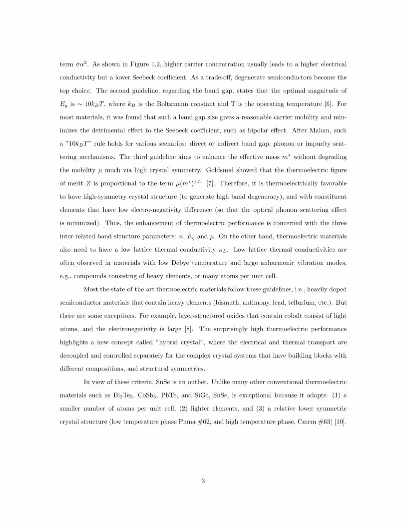
term σα2. As shown in Figure 1.2, higher carrier concentration usually leads to a higher electrical
conductivity but a lower Seebeck coefficient. As a trade-off, degenerate semiconductors become the
top choice. The second guideline, regarding the band gap, states that the optimal magnitude of
Eg is ∼ 10kBT , where kB is the Boltzmann constant and T is the operating temperature [6]. For
most materials, it was found that such a band gap size gives a reasonable carrier mobility and min-
imizes the detrimental effect to the Seebeck coefficient, such as bipolar effect. After Mahan, such
a ”10kBT” rule holds for various scenarios: direct or indirect band gap, phonon or impurity scat-
tering mechanisms. The third guideline aims to enhance the effective mass m∗ without degrading
the mobility µ much via high crystal symmetry. Goldsmid showed that the thermoelectric figure
of merit Z is proportional to the term µ(m∗)1.5 [7]. Therefore, it is thermoelectrically favorable
to have high-symmetry crystal structure (to generate high band degeneracy), and with constituent
elements that have low electro-negativity difference (so that the optical phonon scattering effect
is minimized). Thus, the enhancement of thermoelectric performance is concerned with the three
inter-related band structure parameters: n, Eg and µ. On the other hand, thermoelectric materials
also need to have a low lattice thermal conductivity κL. Low lattice thermal conductivities are
often observed in materials with low Debye temperature and large anharmonic vibration modes,
e.g., compounds consisting of heavy elements, or many atoms per unit cell.
Most the state-of-the-art thermoelectric materials follow these guidelines, i.e., heavily doped
semiconductor materials that contain heavy elements (bismuth, antimony, lead, tellurium, etc.). But
there are some exceptions. For example, layer-structured oxides that contain cobalt consist of light
atoms, and the electronegativity is large [8]. The surprisingly high thermoelectric performance
highlights a new concept called ”hybrid crystal”, where the electrical and thermal transport are
decoupled and controlled separately for the complex crystal systems that have building blocks with
different compositions, and structural symmetries.
In view of these criteria, SnSe is an outlier. Unlike many other conventional thermoelectric
materials such as Bi2Te3, CoSb3, PbTe, and SiGe, SnSe, is exceptional because it adopts: (1) a
smaller number of atoms per unit cell, (2) lighter elements, and (3) a relative lower symmetric
crystal structure (low temperature phase Pnma #62, and high temperature phase, Cmcm #63) [10].
3
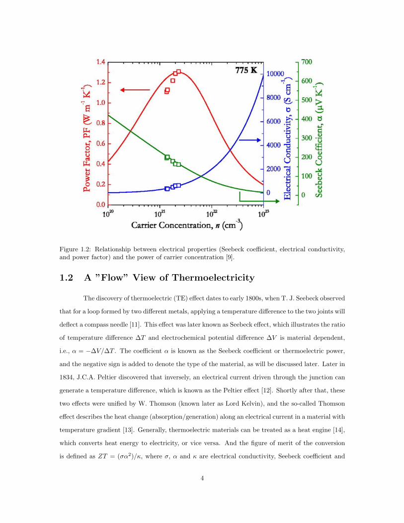
Figure 1.2: Relationship between electrical properties (Seebeck coefficient, electrical conductivity,and power factor) and the power of carrier concentration [9].
1.2 A ”Flow” View of Thermoelectricity
The discovery of thermoelectric (TE) effect dates to early 1800s, when T. J. Seebeck observed
that for a loop formed by two different metals, applying a temperature difference to the two joints will
deflect a compass needle [11]. This effect was later known as Seebeck effect, which illustrates the ratio
of temperature difference ∆T and electrochemical potential difference ∆V is material dependent,
i.e., α = −∆V/∆T . The coefficient α is known as the Seebeck coefficient or thermoelectric power,
and the negative sign is added to denote the type of the material, as will be discussed later. Later in
1834, J.C.A. Peltier discovered that inversely, an electrical current driven through the junction can
generate a temperature difference, which is known as the Peltier effect [12]. Shortly after that, these
two effects were unified by W. Thomson (known later as Lord Kelvin), and the so-called Thomson
effect describes the heat change (absorption/generation) along an electrical current in a material with
temperature gradient [13]. Generally, thermoelectric materials can be treated as a heat engine [14],
which converts heat energy to electricity, or vice versa. And the figure of merit of the conversion
is defined as ZT = (σα2)/κ, where σ, α and κ are electrical conductivity, Seebeck coefficient and
4
Figure 1.3: The relationship between efficiency and heat source temperature TH for different ZTvalues. Here the TC is set to be 300 K. In the figure, it is assumed ZT value is temperatureindependent [15].
total thermal conductivity, respectively. Thus, in order to obtain a high performance TE material,
one needs to enhance the electrical conductivity and Seebeck coefficient, while minimize the total
thermal conductivity. It needs to be noted that the figure of merit ZT is not directly proportional
to the final heat engine efficiency. The relationship between conversion efficiency η and ZT follows
the equation:
η =TH − TCTH
√1 + ZT − 1√
1 + ZT + TC
TH
, (1.1)
where TH and TC are the temperature at the hot and cold ends, respectively. Therefore, as ZT
approaches infinity, the efficiency η gets closer to Carnot efficiency ηC = 1−TC/TH , but never exceeds
it. It is worth noting that some works argued that the actual upper limit of the efficiency should be
Chambadal-Novikov efficiency rather than the Carnot term, and takes the form of η = 1−√TC/TH .
Nonetheless [14], when ZT is higher than 3, an enhancement in ZT will not lead to a significant
increase in the conversion efficiency, as depicted in Figure 1.3.
Comparing with the Carnot efficiency (TH − TC)/TH , the term√
1+ZT−1√1+ZT+TC/TH
in the ex-
pression of η is called irreversible factor [14]. Thus, the goal of thermoelectric research can also be
thought as to increase the irreversible factor as much as possible, approaching the Carnot efficiency
limit.
Onsager proposed that, the thermoelectric process can be treated as two flows: charge and
5

heat [16]. Here, we rewrite the Onsager expressions as
J = −σT(∇µee
)+σTSNT
2
e2∇(
1
T
), (1.2)
JQ = −TσTSN(∇µee
)+
(T 3
e2σTSN
2 + T 2κJ
)∇(
1
T
). (1.3)
Here J is charge flow, JQ is heat flow, σT is electrical conductivity, µe is chemical potential, SN is
Seebeck, T is temperature, κJ is thermal conductivity, e is elementary charge.
And we can find that the thermal conductivity with, zero electrochemical gradient κE , and
zero particle transport κJ , follow the equation
κE = Tα2σT + κJ . (1.4)
Furthermore, with ∇(
1T
)= − 1
T 2∇T and electrical field E = −∇µ/e, we have
J = σTE − σTα∇T, (1.5)
JQ = αTJ − κJ∇T. (1.6)
These are the ”classical” expressions of the two fluxes. We can see that the entropy flow consists
of two terms, αTJ and κJ∇T . And we can find that the ratio between them is the negative of the
figure of merit ZT . That is to say, with a fixed amount of total entropy flow, we need more of the
entropy carried by charge to achieve a higher ZT .
We can further rewrite the thermoelectric figure of merit ZT,
ZT =αJeκT∇T
=1
1− JQαJe
. (1.7)
Here we rewrote J as Je, which is the charge flow. This equation describes thermoelectricity from
the perspective of ”flow”: the figure of merit ZT depends on the ratio of the entropy flow to the
charge flow times coupling term α.
Adopting such a “flow” view provides a deeper insight: (1) the fact that ZT is the ra-
6

tio of the two terms in the expression of entropy flow explains the ”electron-crystal phonon-glass”
paradigm [17]. (2) Other flows such as the spin flow, and the ionic flow can be incorporated into
this framework. In a recent review article [14], Goupil et al. correlated the optimal thermoelectric
performance and the local entropy production, thereby generalizing the thermoelectric process in
specific materials into non-equilibrium coupled dissipative processes. In the context of this gen-
eralized view, a thermoelectric material is no more than a heat engine that uses electrons as its
working medium. In the same vein, the Seebeck coefficient α and the ZT of a material are the
measure of the charge-carried entropy and local entropy production in the given material. The local
entropy production consists of two parts: (i) the heat flow from the hot end to the cold end, and
(ii) the degradation of electrochemical potential into heat, Joule heating is an example [18]. Hence,
enhancing the ZT is hinged upon minimizing the local entropy production: when the local entropy
production is zero, the thermoelectric process becomes reversible, and thus the Carnot efficiency
is attained. And, because of this generalize view of thermoelectric process, the individual thermo-
electric properties can be used not only for calculations of ZT but also probe different aspects of
entropy and charge flows.
Regarding the electrical conductivity, the simplest form is given by the Drude-Boltzmann
expression, σ = neµ, where n and µ are carrier concentration and mobility, respectively. In two
dimensions, a more fundamental expression of σ was given by Landauer [19]. Since the mobility
µ = eh
lkF
, we have σ = 2π e2
hlkF
, where the h,h and kF represent the reduced Planck constant,
the Planck constant and the Fermi vector, respectively. This equation reveals that the electrical
conductivity is directly proportional to the ratio of two length scales: the mean free path of electrons
l, and the Fermi wavelength, λF . Moreover, the Seebeck coefficient given by the Mott relation in two
dimensions can be written as α = π3kB3 (λF
Λ )2. Here Λ represents the de Broglie thermal wavelength,
Λ2 = h2
2πm∗kBT.
We can see that although Seebeck coefficient is one of the material’s transport properties,
it is independent on scattering distance l, and this is consistent with the fact that the Seebeck
coefficient indicates the entropy to charge ratio of each individual electron.
7

1.3 Nature of Seebeck Coefficient
The Seebeck coefficient (i.e., thermopower) is the key transport parameter of thermoelec-
tricity. However, many people often forget the fact that the Seebeck coefficient an independent
transport parameter in its own right, and often confuse the way of how the Seebeck coefficient
is measured with what the Seebeck coefficient tell us. The Seebeck coefficient is defined as also
measured as α = −∆V/∆T , where ∆V and ∆T are electrical potential different and temperature
difference across the materials, respectively. Note the negative sign added here is to make the sign
of the Seebeck coefficient consistent with the sign of the primary charge carriers, which indicates the
conduction type of the material. The positive (negative) sign of Seebeck coefficient is an indicative
of that holes (electrons) are the primary charge carriers. Holes refers to the unoccupied states in the
valence band, so they only ”exist” in the context of band theory. In particular, in a material featured
by multiple band conduction, the Seebeck coefficient and the Hall coefficient might exhibit different
signs as the sign of Seebeck coefficient is dominated by the sign of the carriers with heavier effective
mass whereas the sign of Hall coefficient is dominated by the sign of the carrier with higher mobility.
Since ∆V and ∆T are both directional, the Seebeck coefficient is a 3 × 3 tensor. Regarding the
magnitude, the Seebeck coefficient of a metal is typically ∼ 1− 10µV/K, and for a semiconductor,
the maximum Seebeck coefficient often reaches hundreds of µ V/K. To explore why semiconductors
have much higher Seebeck coefficients than metals, it is helpful to adopt the expression of Seebeck
coefficient by P. M. Chaikin [20]. Basically, the physical meaning of Seebeck coefficient α is the
average entropy carried by one charge carrier, namely,
α =entropy per carrier
charge per carrier, (1.8)
where the charge per carrier is usually the elementary charge e = 1.602×10⁻¹⁹ C. Despite its simple
form, Chaikin’s expression indicates the microscopic meaning of the Seebeck coefficient: entropy per
charge. Many interesting results can be derived from this formula. For example, let’s consider the
expression of entropy in metals and semiconductors. For metals, the heat energy carried by each
carrier is linearly proportional to temperature, with the coefficient equals its molar heat capacity,
c. The molar heat capacity c is also proportional to the temperature, and inversely proportional to
the Fermi energy εF . Thus, for the Seebeck coefficient of metals can be written as α ∝ ce ∝
TεF
.
This indicates that for metals, its Seebeck coefficient is expected to be linearly proportional to
8
temperature over a wide temperature range.
On the other hand, for semiconductors, the heat per charge carrier depends on the difference
between band edge and the chemical potential, which is about half of the band gap Eg/2. And
the entropy is ∼ Eg/2T . Hence, the Seebeck coefficient for a semiconductor is α ∝ Eg
2eT . This
gives the famous Goldsmid-Sharp equation, Eg = 2eαT [21]. Therefore, the Seebeck coefficient of
semiconductors is inversely proportional to temperature, and directly proportional to the magnitude
of the band gap.
Hence from the temperature dependence of the Seebeck coefficient, one can easily distinguish
whether the material is a metal or semiconductor. However, the presence of defects will significantly
impact the behavior in semiconductors and lead to localized states. With defects, a non-periodic
perturbation term is added to the originally perfect periodic Hamiltonian in the system, and as more
and more defects are introduced, the perturbation term is no longer trivial, making the electronic
eigenstates decay spatially, leading to localization. The mechanism of how defects lead to localization
can be found in Chapter 4. In such systems (semiconductors with so many extrinsic defects that is
into a localized state), Chaikin suggested that the temperature dependence of the Seebeck coefficient
follows a power law, where the power factor is a function of the dimensionality of the material d:
α ∝ Td−1d+1 .
Table 1.1 summarizes the temperature dependence of the Seebeck coefficient in some typical
systems. From the figure, we can see that the electronic state in the system largely depends on the
α vs. T . For instance, the α(T ) in a variable range hopping (VRH) system follows a power law,
while superconductor has a Seebeck coefficient of zero. Note a VRH system is not a band conductor,
as electronic states in band conductors are extended, whereas for VRH systems they are localized.
Chaikin’s summary provides rudiments of the Seebeck coefficient. More specifically, if we
assume that (i) the scale of relaxation time is much smaller than the electronic transport, and (ii)
the system is nearly equilibrium, we can linearize Boltzmann equation, which gives us,
α =kBe
∫σ (E) E−EF
kBT
(−∂feq∂E
)dE∫
σ (E)(−∂feq∂E
)dE
. (1.9)
Here σ(E) is the electrical conductivity as a function of energy, following the relation σ(E) =
e2τ(E)v2D(E) and feq is the Fermi-Dirac distribution function. Therefore, the ”entropy” term in
the Seebeck coefficient comes from (i) the change in the density of states (DOS) (ii) the generated
9

General celq or ”heat”
qT
Classical kBq
Metals kBqkBTε
Semiconductors kBq
Eq
2kBT
Variable Range Hoping kBq ( TT0
)d−1d+1
Hubbard Large U Hopping kBq (ln2 + ln 1−ρ
ρ )
Polarons kBq lnρ
Phonon Drag
kBq
1ρ ( TθD )3 Low T
kBq
1ρ ( θDT ) High T
Superconductor 0
Sliding Density Wave 0
Quantum Hall0 filled level
kBε
ln2(N+1/2) 1/2 filled
Table 1.1: The characteristic temperature dependence of Seebeck coefficient [20].
10

entropy from scattering process.
Furthermore, if we assume that the interaction between charge carriers is not strong, one
can obtain the Mott relations [22]:
σ =
∫σ (E)
(−df (E)
dE
)dE, (1.10)
α =π2
3
(kB
2T
e
)(d lnσ (E)
dE
)E=EF
(1.11)
The Seebeck coefficient equation can be further rewritten as
α = −kBe
(η −
(r + 5
2
)Fr+ 3
2(η)(
r + 32
)Fr+ 1
2(η)
), (1.12)
where Fermi-Dirac integral Fn(η) is
Fn (η) =
∫ξn
1 + eξ−ηdξ. (1.13)
As shown, the Seebeck coefficient in its own right is a proper probe to the Fermi surface topology
and its variations. Therefore, we can formalize the Seebeck coefficient for systems with different
band structure and/or conduction mechanisms.
(1) Metals
Metals are materials with finite Fermi surface, that is, the Fermi level crosses the energy
band(s). For metals, the Fermi-Dirac integral Fn(η) can be simplified in a form of polynomial
expression,
Fn (η) =ηn+1
n+ 1+π2
6nηn−1 + . . . . (1.14)
In convention, we only keep the lowest order term in the Fermi-Dirac integral. It accordingly yields
a Seebeck coefficient,
αmetal = −π2kB3e
(kBT
µ
)(3
2+ r
). (1.15)
As shown, the sign of the Seebeck coefficient in metals also depends on the scattering term (3/2+r).
With an energy independent scattering rate, the α is expected to be directly proportional to the
temperature. Also, the µ in metals is often very large, leads to a small magnitude of α. On the
11

other hand, a reasonably high α can be obtained in a low-carrier-concentration metal. In this thesis,
we argue this is the case for SnSe at low temperatures (cf. Chapter 4).
(2) Semiconductors
The chemical potential µ in an intrinsic semiconductor is inside the band gap. With some
calculations, one can show that the Seebeck coefficient for semiconductors follows
αe = − 1
eT
(EC − µ+ kBT
(r +
5
2
)), (1.16)
αh =1
eT
(µ− EV + kBT
(r +
5
2
)). (1.17)
Here the e and h represent the electrons and holes in n- and p-type semiconductors, respectively.
For materials with both types of carriers and their conduction is in parallel with each other, the
overall Seebeck coefficient is
αtot =σeαe + σhαhσe + σh
. (1.18)
Thus, the Seebeck coefficient of semiconductors is not linearly dependent on temperature.
And since α of electrons and holes have the opposite signs, as temperature goes higher, the presence
of both types of carriers will in turn reduce the magnitude of total Seebeck coefficient. This is known
as the bipolar effect, which is generally thought to be detrimental in thermoelectrics.
Notably, the magnitude of band gap in semiconductors can also be estimated from the tem-
perature dependent Seebeck coefficient, according to the Goldsmid-Sharp relation [1]. Meanwhile,
it is worth noting that this relation does not always hold well, as shown in Figure 1.4.
In general, the Seebeck coefficient of a given material is governed by (i) the energy depen-
dence of electronic states, and (ii) the energy-dependent scattering mechanism. An approximate
formula derived from the Bethe-Sommerfeld expansion of the Mott relation for a degenerate single-
band electron system [24] is
α =π2
3
(kB
2T
e
)[1
n
∂n (E)
∂E+
1
µ
∂µ (E)
∂E
], (1.19)
where e is the carrier charge, n is the carrier concentration. While the equation is semi-quantitative
and not applicable in many cases, it is illustrative to note that the stronger the energy-dependence
12
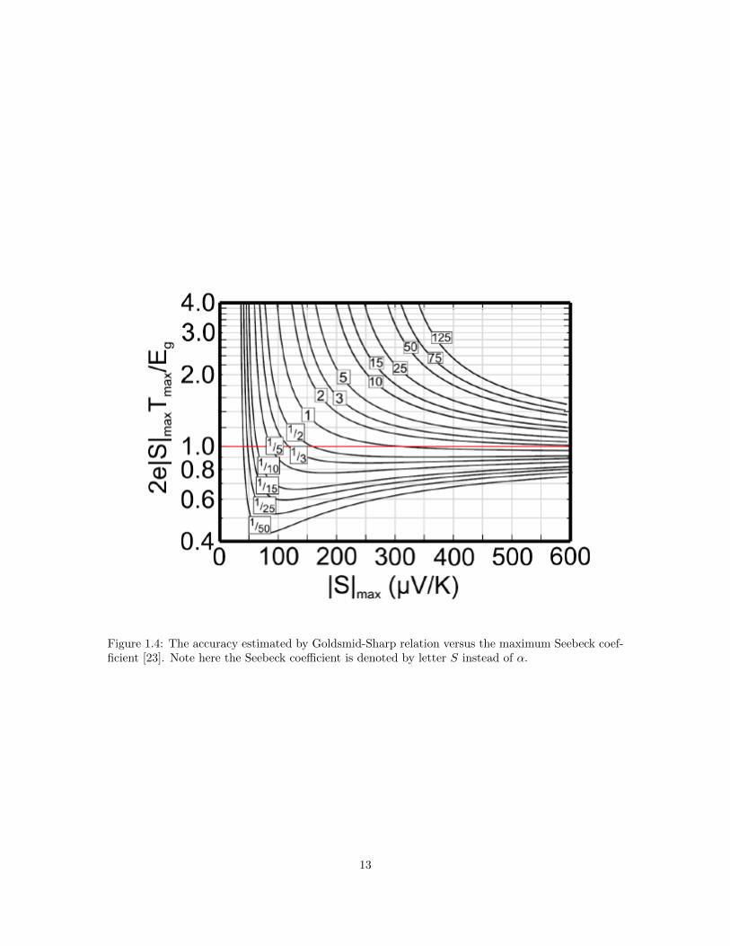
Figure 1.4: The accuracy estimated by Goldsmid-Sharp relation versus the maximum Seebeck coef-ficient [23]. Note here the Seebeck coefficient is denoted by letter S instead of α.
13

of n and µ, the higher the α, i.e., the higher the average entropy carried by a charge carrier. These
conclusions generally hold in more complex materials.
For single band degenerate semiconductors, the Seebeck coefficient can also be expressed in
terms of the effective mass and the carrier concentration,
α =8π2kB
2T
3qh2m∗( π
3n
)2/3
. (1.20)
This is also known as the Pisarenko relation [25].
Therefore, in semiconductors, the Seebeck coefficient is usually not proportional to temper-
ature, and is directly proportional to the effective mass. Also, higher carrier concentration often
leads to lower Seebeck coefficient.
Another important effect is phonon drag. This effect is often observed at low temperatures,
and is caused by the interaction between electrons and phonons. With the phonon drag effect there
is a discernible enhancement in the Seebeck coefficient, and it usually occurs at 1/5 Debye tempera-
ture. Phonon drag is typically stronger at lower temperature and when the carrier concentration is
lower [26]. The measurement of Seebeck coefficient is electrically open-circuited, no charge current
is allowed but heat flow is established under a temperature gradient. The Seebeck effect induced
electrical field accelerates charge carriers, the momenta gained by charge carriers gain are dissipated
in several ways, e.g., some go to the imperfections will eventually turn into heat while some go to
the phonon subsystem. Keep in mind that the phonon subsystem is in non-thermal equilibrium, the
momenta dumped into the phonon subsystem will be retained until non-momentum-conserving pro-
cesses occur. The relaxation time of momentum loss in phonon drag effect is generally longer than
the relaxation time of phonon-phonon interactions. As the phonon drag effects is pronounced at low
carrier concentrations and also low temperatures, we expect the Seebeck coefficient of SnSe, which
is a low carrier concentration metal at low temperatures, would exhibit phonon drag effect [27].
To summarize Chapter 1, we briefly discussed the flow view of thermoelectricity. We showed
that SnSe is an outlier of the traditional material selection criteria for high thermoelectric perfor-
mance. As such, understanding why SnSe possesses high thermoelectric performance would provide
insights into new avenues of developing higher performance thermoelectric materials. To this end,
we need to clarify the intrinsic thermoelectric properties of pristine SnSe, which is still under debate.
In Chapter 2, we will present the results of experimental and theoretical study of high quality single
14
crystalline SnSe in a wide temperature range. These results are unpublished if not otherwise noted.
15

Chapter 2
THERMOELECTRIC
PROPERTIES OF TIN
SELENIDE
2.1 Thermoelectric Properties of SnSe
We start Chapter 2 with a literature survey of the recent works of structural and thermo-
electric study of SnSe. It will be shown that SnSe possesses some peculiar features that distinguishes
it from most peer TE materials. The following discussion will be guided by two questions.
The first question is concerned with the low lattice thermal conductivity, whether the ultra-
low values by Zhao et al. are intrinsic. Most of the state-of-the-art TE materials are semimetals or
semiconductors with complex unit cells and heavy elements, e.g., Bi2Te3, CoSb3. Various approaches
have been developed and implemented to enhance the ZT , e.g., defect engineering, anharmonicity,
band convergence, and cagey semiconductors [28–31]. As a result, the state-of-the-art ZT is around
2. However, although the unit cell of SnSe is not complex, and the atomic weight of Sn and Se
are relative light comparing to many popular TE materials, its ZT was reported to be ∼ 2.6 at
∼ 800 K in pristine SnSe due to ultra-low lattice thermal conductivity even before implementing
any of aforementioned approaches [32]. Notably, whether the reported ZT is indeed that high is still
under debate [33,34] and to our best knowledge, we have not seen other group reproduce this result
16

in pristine SnSe. Nonetheless, it is without doubt that via different techniques such as doping or
nanostructuring, the maximum ZT of SnSe can reach around or above unity [10, 35]. Importantly,
the reported high ZT is mainly owing to its low lattice thermal conductivity. Considering the
relatively light elements and simple unit cell, the nature of the low κL in SnSe single crystals is
worth further investigations.
The other question is concerned with the electronic ground state of SnSe. SnSe was cus-
tomarily regarded to be a p-type semiconductor with a band gap of ∼ 1.0eV [36–38], and its
carrier concentration is only ∼ 6× 1017cm−3 at room temperature [32]. Given a hole concentration
6×1017cm−3, theoretical calculations pointed toward a small but multi-pocket Fermi surface, thus a
metallic ground state. As we will see later in this chapter, there is an anomaly in electrical resistivity
around 50 K. Also, it was found that the Sn vacancies, which contribute holes and thus are expected
to enhance conduction, can drive a metal-insulator transition (MIT).
Therefore, to explore the nature of (1) the low lattice thermal conductivity κL, (2) the
anomaly around 50 K and (3) the MIT of SnSe, the temperature dependent TE properties (the
electrical conductivity, thermal conductivity and Seebeck coefficient) of SnSe are studied from low
temperature to above 900 K in this thesis.
2.2 Previous Works on SnSe
SnSe has been known for decades, and is believed to be an intrinsically p-type semiconductor
with a band gap of ∼ 0.9−1.0eV and a low carrier concentration on the order of 1017−1018 cm−3 [36–
38]. But its application was mainly on optoelectronics and solar cells [39–42], due to its large optical
absorption coefficient [43]. The application of thermoelectrics on SnSe had not been studied for a long
time, owing to the relative high resistivity 10−105 Ωcm. However, a recent study by Zhao et al. [32]
reported an ultra-low thermal conductivity in single crystalline SnSe (< 0.4W/m · K at 923 K),
resulting in a ZT of ∼ 2.6± 0.3 at 923 K, even without doping. Although the single crystallinity of
the SnSe in that work was questioned [33,34], particularly in view of the fact that the packing density
of samples measured therein [32] was only 85% of the theoretical density and the thermal conductvity
reported by Zhao et al. is even lower than that in polycrystalline SnSe samples [35, 44, 45], SnSe
aroused great interest in thermoelectric community. As shown in Figure 2.1, since 2014 after Zhao et
al. work, SnSe surpassed PbTe, SrTiO3, and CoSb3, and became the second popular thermoelectric
17

Figure 2.1: Number of thermoelectric research publications for selected compounds from 1997 to2016.
materials. Numerous studies were conducted to investigate the intrinsic thermoelectric properties
of SnSe, but no consensus has been reached to date.
2.3 Single Crystal Growth and Crystal Structure of SnSe
SnSe adopts a Pmna (No.62) phase at low temperatures. As temperature increases to
Tc ∼ 800 K, it undergoes a second-order phase transition to a Cmcm (No.63) phase, with a higher
symmetry. Notably, the reported Cmcm (No.63) phase is questioned, and will be one of our future
works (cf. Chapter 5). The lattice structures are shown in Figure 2.2. It can be seen that both
phases are layered structure, and adopt van der Waals gaps between the layers. The asymmetric
structure indicates the quasi 2-D behavior of the material, thus TE properties in both in-plane and
out-of-plane directions are expected to anisotropic.
The temperature dependence of the lattice parameters from 65 K to 1014 K is shown in
Figure 2.3. The data were taken on synchrotron X-ray (λ = 0.619925 A, from 300 − 1014 K) at
the beamline BL01C2, National Synchrotron Radiation Research Center, Taiwan. As temperature
approaches from low T to Tc, the lattice parameters along b- and c-axes are approximately the
18

Figure 2.2: The lattice structure of SnSe in (a) Pnma, and (b) Cmcm phases.
same, indicating that Cmcm phase has a higher symmetry. And the continuous change in all three
directions confirms that the transition is second-order. It is worth noting that the thermal expansion
is negative along c-axis, which was attributed to the strong anharmonicity [46]. Another interesting
feature is that the lattice parameter along a-axis is more than twice as large comparing with the
other two directions, thus the TE properties are expected to be quite different along in-plane (the
bc-pane) and out-of-plane direction (a-axis).
SnSe single crystals herein studied were grown with the Bridgeman method at Institute of
Physics, Academia Sinica, Taiwan. Figure 2.4 shows the binary phase diagram of Sn-Se. Sn chunks
(99.999%) and Se shots (99.999%) were sealed in evacuated silica tubes with the stoichiometric ratio
of SnSe. According to the binary phase diagram, the melting is congruent (see Figure 2.4). The
tubes were then placed in a furnace and heated at 1223 K for 48 hours, and then cooled to room
temperature. The obtained ingots were then crushed and sealed in double silica tubes, as the thermal
expansion during growth may break the inner tube, causing oxidization. Vertical Bridgeman method
with a rate of 1.5 mm/h at 1223 K was used to grow SnSe single crystals. The obtained crystals
are about ∼ 50 grams and with a diameter of ∼ 13 mm. Figure 2.5(c) shows an as-grown ingot.
The crystals could be easily cleaved along the (100) face, due to the weak van der Waals bonding.
It is worth noting that for anisotropic systems like SnSe, the direction of the applied temperature
gradient is usually parallel with the axis that has the lowest thermal conductivity, which for SnSe
is a-axis. The crystallinity of the crystals was confirmed via XRD measurements: the XRD pattern
is consistent with theoretical result, and the absence of impurity phases such as SnO2/SnSe2 is
confirmed by Raman spectroscopy.
Since the record-high ZT values were obtained in single crystalline SnSe that have a packing
19

Figure 2.3: Lattice parameters along three axes over a wide temperature range. As mentioned, theactual phase above 800 K in SnSe needs further investigation, here the structure solved and shownin the figure above is still based on a Cmcm space group (unpublished).
20

Figure 2.4: Sn-Se binary phase diagram [47].
density about 85% fo the theoretical density, it is crucial to check the packing density of our as-
grown single crystalline samples. To this end, we used gas pycnometer (Micrometrics ® AccuPyc
II). The measured density of random picked pieces and those pieces for the following transport
measurements showed a density of 6.15± 0.06 g/cm3 at room temperature, within a percent of the
theoretical density 6.18 g/cm3. At room temperature, Archimedes’ method using water yields a
packing density of 6.16±0.01 g/cm3. In addition, the density estimated from the results of Rietveld
refinements of the synchrotron XRD data is around 6.14 g/cm3. These values are close to the
theoretical density. The thermal neutron rocking curves taken at NIST also confirmed the good
crystallinity of as-grown SnSe single crystals (Figure 2.5(a)(b)).
2.4 TE Properties of Single Crystalline SnSe
The electrical conductivity and Seebeck coefficient of SnSe single crystals were measured
from ∼ 14 K to 930 K. Below room temperature the measurement was take on a homemade
resistivity/Seebeck-coefficient (R&S) apparatus [48]. The high temperature part was measured using
the ULVAC ® ZEM-3 system. Around room temperatures, the results in two temperature regions
21

Figure 2.5: (a) and (b): Thermal neutron rocking curves taken on a 19 g single crystal at NIST,Gaithersburg. MD. (c): The single crystal grown by Bridgeman method. Note that the primarycrystallographic axes are not aligned with the quartz tube, rather, there is an angle of about 15degrees. We found this is due to the temperature gradient in the Bridgman furnace.
22

Figure 2.6: The electrical propeties of SnSe single crystals. Left: electrical resistivity; right: Seebeckcoefficient. The discontinuity of the curve along a-axis is discussed in the context.
match well, as shown in Figure 2.6.
For the resistivity, the in-plane direction is more conductive than a-direction, which is as
expected since the presence of van der Waals gap, but the overall trend is similar along all three
directions. Moreover, a turnover can be found around 600 K, below which the materials behaves
like a metal in most regions. From ∼ 600 K to ∼ 800 K, the resistivity decreases with increasing
temperature, while after the phase transition around 800 K, an upturn is observed. The most
interesting part lies below ∼ 50 K. It can be seen in Figure 2.7 that, as temperature decreases to
∼ 50 K, resistivity shows an upturn, i.e., the temperature dependence of resistivity behaves as an
non-metallic, rather than a metal. But whether it is resulted from the disappearance of the Fermi
surface or localization will be elaborated in details in Chapter 4.
The temperature dependence of Seebeck coefficient also shows several turnovers over the
temperature range, as shown in Figure 2.6. Most of these turnovers are concomitant with the
changes in electrical resistivity. Below ∼ 600 K, the Seebeck coefficient increases with temperature.
Between ∼ 600 K and the transition temperature ∼ 800 K, it decreases as temperature increases.
And an upturn occurs after SnSe enters Cmcm phase. Although in most temperature regions, the
temperature dependence of Seebeck coefficient resembles that of resistivity, the behavior is quite
different below ∼ 50 K. Instead of showing an upturn as temperature decreases to ∼ 50 K, Seebeck
coefficient keeps decreasing as temperature cools down, a reminiscent of metallic or hopping behavior.
Moreover, the Seebeck coefficient along a-axis and plausibly b-axis shows a higher slope after crossing
23

Figure 2.7: Electrical resistivity anomaly around 50 K.
∼ 50 K, and approaches zero more quickly, whereas similar behavior is not observed in c-direction.
The possible reasons behind this intriguing behavior will be elaborated in Chapter 4. Regarding the
discontinuity of the Seebeck curve along a-axis, we attribute it to an inefficient heat sinking of the
sample specifically along a-axis. The sample dimension along a-axis was (∼ 5 mm) which is shorter
in length than the optimal length (7 − 8 mm or longer) required for our measurement system. By
contrast, no such problem was encountered along the other two directions as the crystals are long
enough.
It is worth noting that the electrical resistivity measured in this work is very different from
some other reports. For instance, the electrical resistivity reported by Ibrahim et al. is insulating
over a wide temperature range along all three axes [34]. Instead our result is similar to what were
reported Zhao et al. [32]. Again, the cause of such discrepancy will be discussed in Chapter 4.
The total lattice thermal conductivity was also measured in a wide temperature range around
room temperature. The low temperature part was directly measured by a custom designed thermal
conductivity measurement system [49]. And for the high temperature part, the total thermal conduc-
tivity was calculated using κ = Dcvd, where D, cv and d are thermal diffusivity, obtained using the
laser flash technique by Netzsch® LFA-457, specific heat at constant volume, and packing density,
24

respectively. cv was estimated using cp ≈ cv, where cp is the specific heat under consant pressure,
measured on Netzsch® Pegasus 404 high tmemperature differential scanning calorimetry system.
But it is worthnoting that cp ≈ cv only holds for systems without high anharmonicity/thermal
expansion. Hence estimating cv using cp for SnSe needs justification. The measurements of κ were
conducted in all three directions. Since only the low temperature part (using a steady state measure-
ment technique) involves radiation loss [50], a correction was performed on low T region to obtain
the intrinsic total thermal conductivity. As shown in Figure 2.8, the data in two temperature ranges
agree with each other very well.
The lattice thermal conductivity was calculated based on the assumption of κtot = κL +
κe, and Wiedemann-Franz relation, κe = LσT , where κtot, κL, κe are total, lattice, electronic
thermal conductivities, respectively, and L, σ and T are Lorenz number, electrical conductivity and
temperature, respectively. It is worth mentioning that the Wiedemann-Franz relation is not always
valid [22]. Nonetheless, estimating the electronic portion of thermal conductivity can still provide
some insights on the lattice contribution to thermal conductivity. The calculated lattice thermal
conductivity above 300 K is shown in Figure 2.8(b).
We have several interesting observations in Figure 2.8, (1) Both total and lattice thermal
conductivity decrease with increasing temeprature above∼ 30 K, indicating a predominant Umklapp
scattering in that temperature range; (2) An Umklapp peak can be found ∼ 30 K in b- and c-axes,
but absent in a-direction, possibly due to the downshift of the peak in a-xis, since the lattice
parameter (lattice rigidity) in a-axis is much larger (lower) than the other two axes (cf. Figure 2.3).
(3) The magnitude of κL is close to total κ owing to the high electrical resistivity which leads to a low
electronic thermal conductivity. (4) The thermal conductivity measured in this work is consistent
with the report by Ibrahim et al. [34], but significantly lower than the report by Zhao et al. [32].
Other than conventional steady state and laser flash (transient) techniques, the room temperature
thermal conductivity of SnSe was also measured using the time-domain thermo-reflectance (TDTR)
technique (cf. Appendix D). The result is ∼ 0.7± 0.1 W/m ·K at room temperature, slightly lower
than the values measured by the other two techniques. The source of error is likely the smoothness
of surface.
The figure of merit ZT is shown in Figure 2.9. The ZT peaks is found in the Cmcm phase
at 850 K. The values are ∼ 1.0, 0.8 and 0.25 along b, c and a directions, repectively. The obtained
ZT is significantly lower than that of ∼ 2.6 reported by Zhao et al. [32].The discrepancy is mainly
25

Figure 2.8: (a) Total thermal conductivity in log-log scale (inset: total thermal conductivity in linearscale), and (b) lattice thermal conductivity of SnSe single crystals.
26
due to the difference in the measured κ in two works. As reported by Wei et al. [33], the high
ZT in Zhao et al.’s work [32] is possibly due to the low packing density of their crystals, thus their
measured thermal conductivity is not intrinsic. Since the packing density of the crystals in this work
is > 99% of the theoretical density, the magnitude of our measured κ is well justified, and it is still
low enough comparing with most other materials.
Other than the pristine SnSe crystals, we also prepared samples with intentionally intro-
duced Sn deficiency, Sn0.99Se and Sn0.94Sn. The temperature dependence of electrical resistivity is
shown in Figure 2.10. Intuitively, adding more Sn deficiency introduces Sn vacancies, which con-
tribute holes to the system, and making the material more conductive. This is indeed the case
for Sn0.99Se sample. However, it was found that for Sn0.94Se, the resistivity shows an insulating
behavior. Thus, we found a metal-insulator transition (MIT) driven by Sn vacancies. The possible
origin of this phenomenon will be discussed in Chapter 4.
Chapter 2 presents a whole picture of the thermoelectric properties of single crystalline
prinstine SnSe. From now on, our main focus would be on elaboration of the three primary questions:
(1) Why the thermal conductivity of SnSe is low? (2) What is the nature of the resistivity anomaly
around 50 K? (3) What is the nature of the MIT driven by Sn vacancies? We will implement both
experimental and theoretical studies to answer these questions in the following two chapters.
27

Figure 2.9: Figure of merit ZT of SnSe single crystals along three directions.
28

Figure 2.10: Temperature dependence of electrical resistivities for SnSe samples with different Sndeficiency.
29
Chapter 3
LOW THERMAL
CONDUCTIVITY IN TIN
SELENIDE
In this chapter, we will explore the origin of the low thermal conductivity in SnSe single
crystals. First, several low thermal conductivity materials are introduced. Then we will discuss the
possible origins of the low κ in SnSe, using both experimental and theoretical techniques.
3.1 Mechanisms Underlying Low Thermal Conductivity
Since heat is carried by phonons in crystals, there are two approaches to suppress thermal
conduction: (1) Reducing phonon mean free path in space domain; (2) Reducing phonon life time
in time domain.
3.1.1 Brief Introduction to Thermal Conductivity
Thermal conductivity is defined as the negative of heat flux to temperature gradient ratio,
i.e., κ = − ~Q~∇T
. Since the heat flux can be phenomenologically expressed as
~Q = −1
3ncτv2~∇T, (3.1)
30
where n, c, τ , v are particle density, heat capacity per particle, relaxation time, and mean particle
velocity, respectively. Here nc could be further written as the heat capacity per unit volume cV /Vm =
nc, where cV is the molar heat capacity at constant volume and Vm is the molar volume. vτ could also
be written as the particle mean free path l = vτ . Therefore, the thermal conductivity κ = 13CV vl.
From a microscopic perspective, the heat flux is carried by phonons. As a type of quasi-
particle, phonons represent the collective excitation in a periodic lattice. In an ideal crystal where
the interatomic force is purely harmonic, i.e., only quadratic term presents in the force constant, all
phonon modes are eigenstates and have infinite life time. At thermal equilibrium, the distribution
function of phonons follows Bose-Einstein model,
f (ω) =1
exp(hωkBT
)− 1
. (3.2)
If we assume the phonon frequency is linearly dependent on the wave vector (i.e., long wavelength
acoustic phonons or elastic waves), ω = ck, we obtain the Debye model
U =9NkBT
4
TD3
∫ TD/T
0
x3
ex − 1dx, (3.3)
CV = 9NkB
[T
TD
]3 ∫ TD/T
0
x4ex
(ex − 1)2 dx. (3.4)
Here U and CV are the internal energy and heat capacity at constant volume, respectively. N is the
number of atoms. TD is Debye temperature, defined as TD = hνDkB
, corresponding to the maximum
allowed phonon frequency νD. Debye temperature can also be treated as a gauge of the lattice
rigidity in a material. At low temperatures, one can show that the heat capacity at constant volume
follows
CV =12π4
5NkB
(T
TD
)3
. (3.5)
Hence CV ∼ T 3 when the Debye model holds. On the other hand, as temperature goes higher,
CV = 3NkB , i.e., it saturates at the so-called Dulong-Petit limit.
In crystals, the heat is mostly carried by phonons. As bosons, the behavior and nature
of phonons can be examined with the phonon dispersion relation (cf. Chapter 3 for the phonon
dispersion relation of SnSe). And in the simplest case, the angular frequency ω of acoustic phonons
31
is linearly proportional to moment k, the Debye model, whereas optical phonons obey Einstein rule,
ω equals to a constant k-independent angular frequency ω0.
3.1.2 Factors That Limit Phonon Mean Free Path
The most effective way to suppress κ is via frequent phonon scattering, which significantly
shortens the phonon mean free path. Ideally, phonons have an infinite long relaxation time, thus
the mean free path l ∼ ∞. But in real crystals, various approaches will scatter the phonons so that
the relaxation time is finite. If we assume the scattering mechanisms are independent of each other
and they affect the relaxation time in a parallel way, we can express the total relaxation time τtotal
as
1
τtotal=
1
τPD+
1
τB+
1
τU+
1
τPE+ · · · . (3.6)
This formula is also known as Matthiessen’s rule [51]. Here the subscripts represent different
phonon scattering processes: PD, B, U and PE stand for the scattering by point defects, boundaries,
other phonons, and electrons, respectively. There exist other possible scattering mechanisms such
as phonon-magnon relaxation but these four types are usually most important. Callaway model of
thermal conductivity is based on the assumptions that the longitudinal and transverse polarizations
are identical [52]. If we neglect the correction term for normal ph-ph scattering process (N-process),
a simplified Callaway model can be described as,
κ =kB
2π2v
(kBh
)3
T 3
∫ θD/T
0
τ (x)x4ex
(ex − 1)2 dx, (3.7)
where x = hω/κBT , v is the phonon velocity, and θD is the Debye temperature. Here Debye
temperature θD =v(6π2n)
1/3
κB, where n is the number of atoms in a unit volume.
As mentioned above, typically, thermal conductivity is reduced by ph-ph scattering, ph-e
scattering, point defect scattering and boundary scattering. The effects of these scattering processes
reflect in the term τ(x) in Callaway model. Below we will give the equations to estimate the
relaxation time of phonons due to each of the four scattering mechanisms.
(1) Umklapp scattering
Phonon-phonon scattering, also known as Umklapp scattering process, is crucial at temper-
atures T > 0.1θD [53]. It originates from the three-phonon scattering process where two phonons
32

Figure 3.1: Normal process (N-process) and Umklapp process (U-process).
anharmonically interact with each other and create a new phonon with different energy and mo-
mentum. If the new phonon has a wave-vector −→κ greater than the length of the first Brillouin zone,
it will be equivalent to a phonon that has a wave-vector−→κ′ = −→κ +
−→G . Here
−→G is the reciprocal
lattice vector. Figure 3.1 illustrates the two types of ph-ph scattering processes. In Normal process,
the generated new phonon is within the first Brillouin zone, thus the total momentum and energy
are conserved. Whereas in Umklapp process, the new phonon after shifted by−→G is travelling in the
opposite direction. Hence in U-process, the ph-ph scattering significantly suppresses the thermal
conduction.
The relaxation time due to Umklapp scattering is given by
τU−1 =
hγ2$2T
Mv2θDexp
(−θD
3T
), (3.8)
where γ is the Grueneisen parameter, and M is the average mass. Grueneisen parameter is closely
related to thermal expansion coefficient, and is also a gauge of the anharmonicity of the interatomic
bonding: γ = 3βBmVm
CV. Here β, Bm, Vm and CV are linear thermal expansion coefficient, isothermal
bulk modulus, the molar volume and heat capacity, respectively. The isothermal bulk modulus
depends on the transverse sound velocity vt, and density ρ, Bm = vt2ρ.
(2) Point defect scattering
Phonons can be scattered by point defects, since the phonon modes that carry heat are no
33

longer eigenstates in the vicinity of point defect. This effect of point defect scattering on thermal
conductivity reduction comes from two parts: the mass difference τM and strain difference τS within
the lattice. The resulted τPD is then given by [54]
τPD−1 = τM
−1 + τS−1 =
V $4
4πv3(ΓM + ΓS) , (3.9)
where ΓM and ΓS are the disorder scattering parameters due to the mass and strain fluctuation
across the lattice, respectively. An example of adopting the disorder scattering parameters in cal-
culating τPD can be found in Ref. [55]. The point defects (e.g., native Sn vacancies in the case
of SnSe), unless present in a large amount, would not affect the lattice thermal conductivity at low
temperatures because heat is carried by long wavelength phonon modes at low temperatures. But
the phonon-point defect scattering become more significant at high temperatures.
(3) Phonon-electron scattering
Electrons in the system can also reduce thermal conductivity via the interactions with
phonons. In the case the band structure of electrons is parabolic and carrier concentration is not
low, i.e., the ph-e interaction is not negligible, the relaxation time due to phonon-electron scattering
is given by [56],
τpe−1 =
Edef2m∗2ω
2πh3ρv1
. (3.10)
Here Edef is the deformation potential; m∗ is the effective mass of electrons; ω and ρ are the
frequency and density, respectively.
(4) Boundary scattering
Another mechanism that scatters phonons is boundary scattering. The relaxation time due
to boundary scattering depends on the grain size d and the velocity of phonons v, via τB = d/v.
The τB contribution to total thermal conductivity is non-trivial in polycrystalline materials or thin
films [54].
Those are the four main mechanisms that limit the thermal conductivity via shortening the
phonon mean free path. An example of the frequency dependence of the corresponding relaxation
time due to each scattering process is plotted in Figure 3.2. It can be shown that the ω dependence
of τ follow: τPD ∝ ω−4, τU ∝ ω−2, τPE ∝ ω−2, and τB is independent of ω.
34
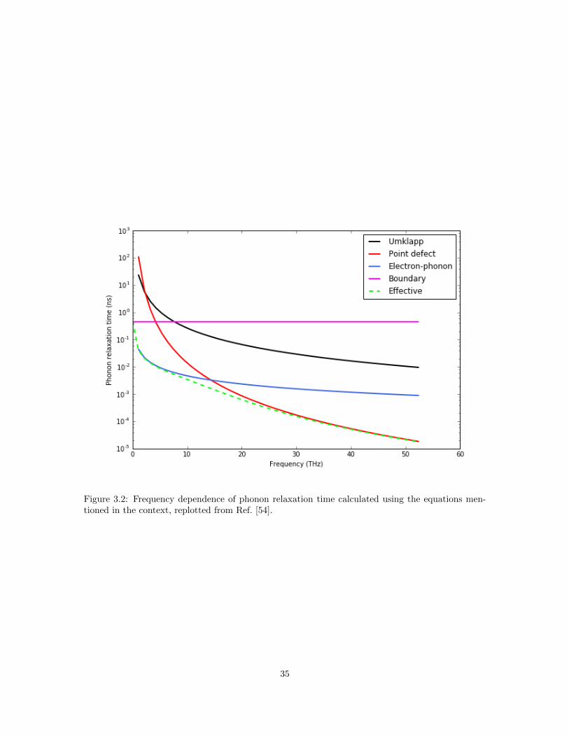
Figure 3.2: Frequency dependence of phonon relaxation time calculated using the equations men-tioned in the context, replotted from Ref. [54].
35

3.1.3 Anharmonicity That Limits Phonon Life Time
Above we discussed the scattering-limited phonon mean free path, which is the space do-
main. In this section, we investigated a mechanism that limits the phonon life time in the time
domain, called ”anharmonicity”.
If the force between atoms is linearly proportional to the inter-atomic distance, the system is
harmonic. In a harmonic system, the phonon modes have distinct energy levels and infinite lifetime.
Also, there is no phonon-phonon interaction, since all phonon modes are eigenstates of the system.
However, for a system with strong anharmonicity, the higher order terms occur in the interatomic
bonding, so that: (1) As temperature goes higher, the mean position of atomic vibrations deviates
from that at 0 K, leading to the thermal expansion effect; (2) The phonon modes of harmonic
bonding are no longer the eigenstates, and thus have finite lifetime. The finite lifetime can also be
understood by the presence of ph-ph interaction as the bonding becomes anharmonic.
The anharmonicity of a material can be quantitatively and qualitatively determined by
several techniques, such as thermal expansion measurements, and the difference between specific heat
at constant pressure CP and at constant volume CV . These methods are related to the dimensionless
Gruneisen parameter γ, which can be defined by several formulae,
γ = V
(dP
dE
)V
=αKT
CV ρ=αKS
CP ρ=αvs
2
CP, (3.11)
where α is the volume thermal expansion coefficient, KS and KT are the adiabatic and isothermal
bulk moduli, vs is the sound velocity. A large γ indicates a strong anharmonicity. As mentioned
above, the calculated γ in SnSe is about 4 over a wide temperature range. This is not a low value,
especially considering it is the averaged value over phonons with different momentum and modes.
Such a value indicates a non-trivial anharmonicity effect in SnSe. Also, the actual anharmonicity
might be stronger that the calculated Gruneisen parameter indicates, because along one of the three
axes, SnSe is shrinking as temperature increases, which compensates the expansion effect along the
other two directions when calculating volume thermal expansion coefficient.
Specific heat not only appears in the phenomenological equation κ = 13CV vl but also pro-
vides insights of the phonon modes. The specific heat at constant pressure CP of single crystalline
SnSe was measured from 0.45875 K. From 0.452 K, CP was measured with a 3He cryostat, and
from 2300 K was measured using a Quantum Design® Physical Properties Measurement System.
36

Figure 3.3: (a) Molar heat capacity cP of SnSe as a function of temperature. The red dottedhorizontal line is the Dulong-Petit limit. (b) cP /T vs. T 2 below 1 K (c) cP vs. T below 11 K. Thetwo solid curves denote the fitting results using two different models.
These two measurements were conducted in Institute of Physics, Academia Sinica in Taiwan. Above
300 K the specific heat was measured using Netzsch® Pegasus 404 high temperature differential
scanning calorimetry system. The result is shown in Figure 3.3.
The measured cP falls on the values expected for the classical Dulong-Petit limit, which
is the limit of cV . At first glance, it seems to suggest the anharmonicity diminishes. However,
the temperature dependence of crystal lattice constants clearly shows that the thermal expansion
persists into the regime above the phase transition, indicating strong anharmonic effect.
A distinct lambda-shaped peak at ∼ 800 K confirms the second order phase transition be-
tween the Pnma and Cmcm phases. The red dotted line indicates the Dulong-Petit limit calculated
for SnSe, which equals 49.9 J/mol · K. It can be seen that CP exceeds Dulong-Petit limit in the
temperature range of 300800 K. The difference between CP and D-P limit could be explained by
a strong anharmonicity, since the D-P limit describes specific heat at constant volume CV , while
37

CP = CV + V T α2
βT. Here α = 1
V (∂V∂T )P is the thermal expansion coefficient, which is closely related
to the anharmonicity in the material. βT = − 1V (∂V∂P )T is the isothermal compressibility, which is
equivalent to the bulk modulus. In the Cmcm phase, CP retains the D-P limit, which could be
explained by the presence of the phonon softening that offsets the effect of anharmonicity. The
phonon softening was observed previously in neutron scattering measurements [57], and we will
further investigate it in the following.
The specific heat generally contains two terms: the electronic contribution and the lattice
part. At sufficiently low temperatures (much lower than Debye temperature), one can assume that
Debye model is valid, and the anharmonicity is negligible. Then the specific heat can be expressed as
C = Celectron +Clattice = γT + βT 3. Here γ is the Sommerfeld constant, and β = 12π4
5 nNAkBθD−3
can be used to estimate Debye temperature. Figure 3.3(b) plots cP below 1 K, where the fitted
parameters are γ ∼ 4.65×10⁻⁵ Jmol−1K−2, and β ∼ 4.57×10⁻⁴ Jmol−1K−4. The low Sommerfeld
constant value indicates a low electronic DOS at Fermi level. From the value of β, a θD ∼ 204 K
can be obtained. Furthermore, with θD = ( 3N4πV )(1/3)hvskB
, where N/V is the number of atoms per
unit volume, we obtained a sound velocity of vs = 2619 m/s. This value agrees with the previously
reported sound velocity from neutron scattering experiment [57].
Although a Debye model is sufficient to explain the specific heat behavior below 1 K, it is
found that as temperatures goes up to 5−10 K range, even though the temperature is still far below
Debye temperature, a distinct deviation from the Debye model is evident, as shown in Figure 3.3(c).
However, by adding a single Einstein term, C (θE) = A(θE/T )2e(θE/T )/
(e(θE/T ) − 1
)2where the
Einstein oscillation temperature θE ∼ 57.5 K, the resulted fitting CP = CDebye + CEinstein can
then describe the measured Cp data. Unlike Debye model where the phonon dispersion relation is
linear, ωD = ck, the phonon frequency in Einstein model is independent of its momentum, and each
Einstein phonon mode has a fixed value over the whole k-space. Debye model is found to be able to
describe the signature of acoustic phonons with long wavelength, whereas Einstein model is often
used for optical phonon modes. In most materials, the optical phonon modes have a significantly
higher energy than acoustic phonon branches when wavelength is long (i.e., near zone center), thus
Debye model alone can describe the temperature dependence of CP at low temperatures. However,
the CP fitting shown in Figure 3.3 indicates that in SnSe, there is an optical phonon mode that also
accounts for the total specific heat. The fitted Einstein temperature of ∼ 57.5 K corresponds to a
frequency of ∼ 1.2 THz, in a good agreement to the inelastic neutron scattering study [57].
38
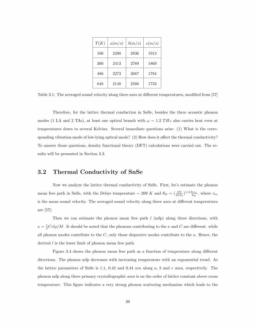
T (K) a(m/s) b(m/s) c(m/s)
100 2490 2836 1913
300 2413 2789 1869
486 2273 2687 1794
648 2148 2586 1733
Table 3.1: The averaged sound velocity along three axes at different temperatures, modified from [57]
Therefore, for the lattice thermal conduction in SnSe, besides the three acoustic phonon
modes (1 LA and 2 TAs), at least one optical branch with ω ∼ 1.2 THz also carries heat even at
temperatures down to several Kelvins. Several immediate questions arise: (1) What is the corre-
sponding vibration mode of low-lying optical mode? (2) How does it affect the thermal conductivity?
To answer those questions, density functional theory (DFT) calculations were carried out. The re-
sults will be presented in Section 3.3.
3.2 Thermal Conductivity of SnSe
Now we analyze the lattice thermal conductivity of SnSe. First, let’s estimate the phonon
mean free path in SnSe, with the Debye temperature ∼ 209 K and θD = ( 3N4πV0
)1/3 hvmkB
, where vm
is the mean sound velocity. The averaged sound velocity along three axes at different temperatures
are [57]:
Then we can estimate the phonon mean free path l (mfp) along three directions, with
κ = 13Cvlρ/M . It should be noted that the phonons contributing to the κ and C are different: while
all phonon modes contribute to the C, only those dispersive modes contribute to the κ. Hence, the
derived l is the lower limit of phonon mean free path.
Figure 3.4 shows the phonon mean free path as a function of temperature along different
directions. The phonon mfp decreases with increasing temperature with an exponential trend. As
the lattice parameters of SnSe is 1.1, 0.42 and 0.44 nm along a, b and c axes, respectively. The
phonon mfp along three primary crystallographic axes is on the order of lattice constant above room
temperature. This figure indicates a very strong phonon scattering mechanism which leads to the
39

Figure 3.4: Estimated phonon mean free path along three primary crystallographic axes of SnSe.
ultra-low thermal conductivity in SnSe. Also, above room temperatures, the reduction of thermal
conductivity in SnSe can be attributed to the decreasing phonon mean free path, while the specific
heat and speed of sound don’t change much as temperature increases.
How heat-carrying phonons are scattered in SnSe? As discussed above, there are at least four
scattering mechanisms that can reduce the phonon mean free path. For the single crystalline SnSe
samples studied in this work, the contribution of point defects and grain boundaries can be excluded.
Moreover, as the Hall measurements gives a weakly temperature dependent low carrier concentration
n ∼ 1017 cm−3 (shown in Chapter 4) from 2 K to 310 K, whereas the lattice thermal conductivity
exhibits the electron-phonon (e-ph) scattering is assumed to be not important. Certainly, one
can examine the Raman peak broadening in the context of Wigner-Fanno-Breit formulism, which
provides a gauge of the e-ph coupling [58]. The e-ph coupling may be also reflected in the phonon
drag effect. In the low temperature Seebeck coefficient of SnSe, we do not see any signature of phonon
drag, suggesting a weak e-ph coupling in SnSe (cf. Chapter 4). Therefore, it is plausible to argue
that the most important scattering mechanism is phonon-phonon interaction in single crystalline
SnSe. Since Umklapp process (U-process) is more significant on reducing κ than Normal process,
we have τtotal ≈ τU .
40

Now we try to estimate the U-process in SnSe. There are various reported values of Debye
temperature θD for SnSe, ranging from ∼ 24 − 65 K [32], to ∼ 175 K [59]. The specific heat
measurement performed in this work gives a Debye temperature of ∼ 204 K (shown later in this
chapter), which we will be using in the calculation of τU . The volume thermal expansion coefficient
in SnSe can be calculated from the lattice parameter vs. temperature plot, α = 1VdVdT , and it
gives α ∼ 2.9 × 10⁻⁵ K−1 (cf. Figure 3.5). The Grueneisen parameter γ can then be solved via
γG = 3βBmVm
CV= αvt
2Mm
CV. For simplicity and without losing much generality, we used the Dulong-
Petit limit for Cv, and the sound velocity is a constant ∼ 2600 m/s. The calculated γG is around
4 over a wide temperature range, which is close to the values reported by Zhao et al. [10]. It
is worth noting that the value is mode-averaged, as, for instance, the linear thermal expansion is
quite different along three axes. And since the linear thermal expansion is negative along c-axis,
which mitigates the expansion effect along the other two directions, the calculated volume thermal
expansion coefficient might not be a ”good” gauge of Gruneisen parameter. Nonetheless, the large
Gruneisen value indicates a strong anharmonicity in SnSe, which will be discussed later in this
chapter.
Figure 3.6 plots the calculated τU vs. ω, and calculated temperature dependence of thermal
conductivity. Here we also plotted the reduced phonon relaxation time due to e-ph scattering, to
demonstrate that in SnSe single crystals, Umklapp process is predominant. The parameters used
in calculating τPE can be found in Ref. [60]. It is apparent in Figure 3.6(a) that the phonon relax-
ation time is almost solely dependent on Umklapp scattering. Figure 3.6(b) plots the temperature
dependence of thermal conductivity based on the calculated U-process result. We can find that the
calculated value is several times greater than the experimental data. Possible explanations include:
(1) Other scattering mechanisms are not taken into account; (2) The simplified Callaway formula
is insufficient to account for the behavior of phonons in SnSe. Other models such as the original
Callaway theory, or Allen model (a modified version of the Callaway model [61] should be used. (3)
The Normal process, i.e., the type of ph-ph interaction where the generated phonon is still within
the first Brillouin zone, is not negligible. In fact, Al-Otaibi et al. studied the three-phonon scat-
tering process in some IV-chalcogenides [62]. It was found that the relaxation time due to N- and
U-processes strongly depends on the location of phonon wavenumber in the Brillouin zone, that is to
say, τU−1/τN
−1 is substantially dependent on x = q/qD. For low wavenumber phonons, τU−1/τN
−1
is typically less than 0.5, i.e., N-process is more prominent. While as the wavenumber approaches
41
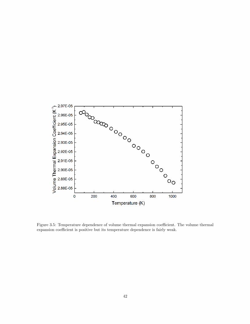
Figure 3.5: Temperature dependence of volume thermal expansion coefficient. The volume thermalexpansion coefficient is positive but its temperature dependence is fairly weak.
42
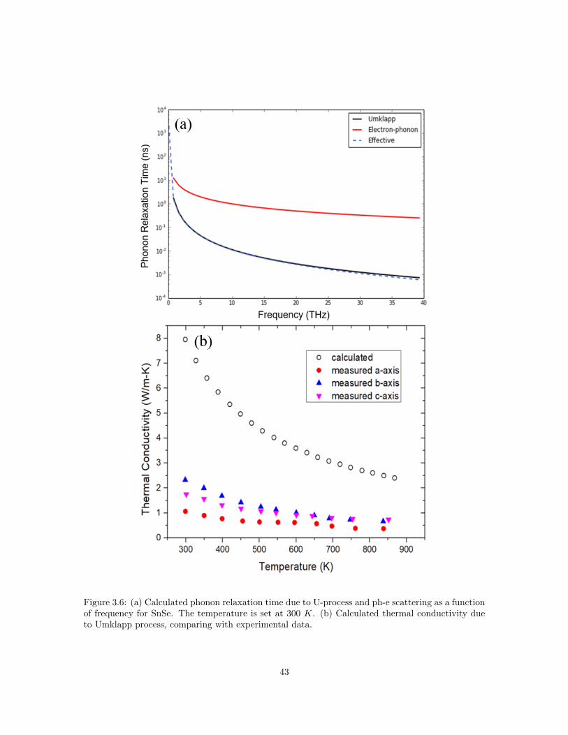
Figure 3.6: (a) Calculated phonon relaxation time due to U-process and ph-e scattering as a functionof frequency for SnSe. The temperature is set at 300 K. (b) Calculated thermal conductivity dueto Umklapp process, comparing with experimental data.
43

Figure 3.7: Comparison of Umklapp and Normal scattering rates in PbTe and SnTe at 300 K. Takenfrom [62].
the zone edge, τU−1/τN
−1 increases. Hence the relative weight of N-process and U-process varies
at different k values. Other than the wavenumber, it was found that τU−1/τN
−1 are also mode-
dependent, e.g., longitudinal/transverse, and/or acoustic/optical. Figure 3.7 shows the calculated
τU−1/τN
−1 for PbTe and SnTe at 300 K. It can be seen that Umklapp process becomes more
important as the phonon mode gets closer to zone boundary.
Therefore, to understand the origin of the low thermal conductivity in SnSe, it is crucial to
investigate the detailed phonon modes and the possible interactions between them, or equivalently,
the anharmonicity in the material. The fact that the estimated thermal conductivity due to Umklapp
scattering is several times greater than the measured value, may imply a native scattering mechanism
that may be associated with long wavelength (low k) phonons. Because phonons close to Brillouin
zone center is usually not sensitive to the Umklapp process yet carries significant amount of heat,
effectively scattering those phonons could strongly reduce the thermal conductivity even without
the presence of Umklapp scattering. In the rest of this chapter we will carry out both experimental
measurements and theoretical calculations to study the phonons in SnSe with the emphasis on those
44
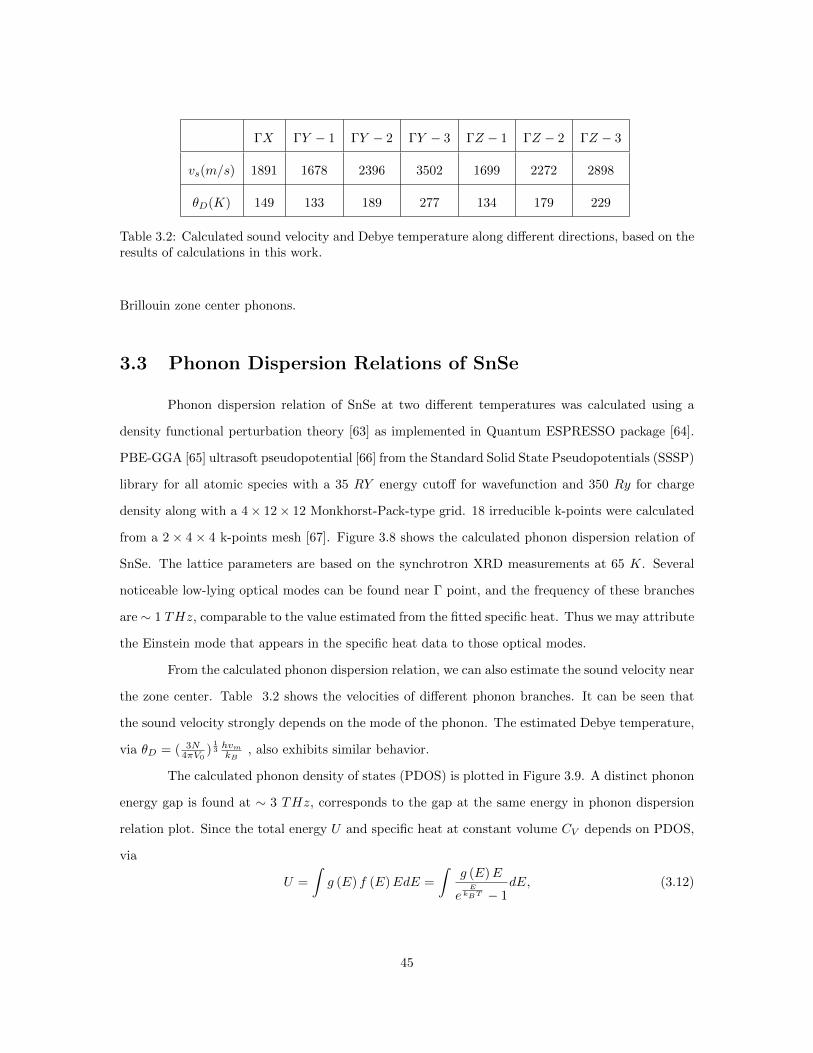
ΓX ΓY − 1 ΓY − 2 ΓY − 3 ΓZ − 1 ΓZ − 2 ΓZ − 3
vs(m/s) 1891 1678 2396 3502 1699 2272 2898
θD(K) 149 133 189 277 134 179 229
Table 3.2: Calculated sound velocity and Debye temperature along different directions, based on theresults of calculations in this work.
Brillouin zone center phonons.
3.3 Phonon Dispersion Relations of SnSe
Phonon dispersion relation of SnSe at two different temperatures was calculated using a
density functional perturbation theory [63] as implemented in Quantum ESPRESSO package [64].
PBE-GGA [65] ultrasoft pseudopotential [66] from the Standard Solid State Pseudopotentials (SSSP)
library for all atomic species with a 35 RY energy cutoff for wavefunction and 350 Ry for charge
density along with a 4× 12× 12 Monkhorst-Pack-type grid. 18 irreducible k-points were calculated
from a 2 × 4 × 4 k-points mesh [67]. Figure 3.8 shows the calculated phonon dispersion relation of
SnSe. The lattice parameters are based on the synchrotron XRD measurements at 65 K. Several
noticeable low-lying optical modes can be found near Γ point, and the frequency of these branches
are ∼ 1 THz, comparable to the value estimated from the fitted specific heat. Thus we may attribute
the Einstein mode that appears in the specific heat data to those optical modes.
From the calculated phonon dispersion relation, we can also estimate the sound velocity near
the zone center. Table 3.2 shows the velocities of different phonon branches. It can be seen that
the sound velocity strongly depends on the mode of the phonon. The estimated Debye temperature,
via θD = ( 3N4πV0
)13hvmkB
, also exhibits similar behavior.
The calculated phonon density of states (PDOS) is plotted in Figure 3.9. A distinct phonon
energy gap is found at ∼ 3 THz, corresponds to the gap at the same energy in phonon dispersion
relation plot. Since the total energy U and specific heat at constant volume CV depends on PDOS,
via
U =
∫g (E) f (E)EdE =
∫g (E)E
eE
kBT − 1dE, (3.12)
45

Figure 3.8: Phonon dispersion relation of SnSe calculated using DFT, calculated by Drs. Ching-MingWei and Chen-Rong Hsing in Taiwan.
46

Figure 3.9: Calculated PDOS of SnSe at 65 K. The resemblance of the PDOS between 0 and 3 GHzand that above 3 GHz is due the softening of zone center optical mode, which mimics the dispersionof an acoustic mode.
CV =
(∂U
∂T
)V
=
∫g (E)E2e
EkBT
kBT 2(e
EkBT − 1
)dE, (3.13)
where g(E) denotes the PDOS, and f(E) is Bose-Einstein distribution function, we can calculate
for CV and compares it with our experimental data.
The calculated specific heat are plotted in Figure 3.10. Some noteworthy remarks are:
(1) The calculated Cv is close to the measured Cp over a wide range of temperatures. As
temperature goes higher, Cv approaches the Dulong-Petit limit.
(2) Theoretically, the Cp should be no less than that the Cv. However, this is not the case
below 125 K. One possible scenario is that the calculated Cv is based on PDOS at 65 K and we
assume that the PDOS doesn’t vary with temperature. Nonetheless, we found that at T > θD, the
Cp is noticeable greater than the Cv and also the D-P limit, and the difference between them gets
larger as temperature increases. This phenomenon is a clear signature of strong anharmonicity in
SnSe.
(3) Figure 3.10(d) shows the fitted C/T vs. T at ultra-low temperatures. By fitting the
47

Figure 3.10: (a-c) Comparison of measured (CP ) and calculated (CV ) specific heat at differenttemperature ranges. (d) C/T vs. T 2 plot for both measured and calculated data.
calculated data and using , we obtain a Debye temperature of ∼ 182 K, which is close to our
experimental value 204 K (fitted with experimental Cp data).
For the vibration mode that the optical phonons represent, Li et al. [57] attribute it to
TOc mode, as illustrated in Figure 3.11. Li et al. suggested this atomic motion accounts for most
of the anharmonic effect in SnSe, greatly suppresses its thermal conductivity. Therefore, the low-
lying optical phonons found in both Cp measurement and phonon dispersion relation calculations
represents the TOc mode, and the corresponding atomic motion is illustrated in Figure 3.11. Next,
we will discuss how the presence of this low energy optical mode affects thermal conductivity, and
also why this particular mode has such a low energy and strong anharmonicity. Above we have
demonstrated that for SnSe single crystals, except for phonon-phonon interactions, all the other
phonon scattering mechanisms are negligible. More specifically, the interaction is between TOc mode
and acoustic phonons. The reason for them to interact originates from the fact that the interatomic
force constant is not purely harmonic and contains higher order terms. To verify the existence of
ph-ph coupling, further experiments such as inelastic neutron scattering is needed. Ideally, for strong
anharmonic systems, the corresponding phonon modes should have a wide linewidth, as energy and
48

Figure 3.11: The displacement pattern for the lowest-energy TOc mode (Pnma) in SnSe, taken fromRef. [57].
time are conjugate to each other according to Heisenberg uncertainty principle. A broad linewidth
indicates a short lifetime of that phonon mode.
In addition, avoided crossing of the coupled phonon modes may be observed in the measured
phonon dispersion relation. Basically, avoided crossing indicates the presence of perturbation to the
Hamiltonian which contains off-diagonal elements. Neumann and Wigner demonstrated that the
two phonon branches would not cross if they belong to the same irreducible representation (i.e.,
symmetry) [68]. The avoided crossing is found to lower the group velocity where the phonon bands
avoid crossing, thereby reducing the thermal conductivity [69]. In the case of SnSe, for example, the
higher order terms in interatomic force constant can be treated as the perturbation to the harmonic
Hamiltonian. This results in a split in the originally degenerate states at crossing point. Moreover,
after avoided crossing, the new states are mixture of the original degenerate eigenstates. In fact, as
can be seen in Figure 3.8, the avoided crossing between acoustic and low-lying optical modes in SnSe
is found for some phonon states, for example, the phonon modes along Γ− T direction at around 1
THz. But the crossing in some directions (e.g., Γ− Y ) is not evidently avoided. Nonetheless, direct
experimental measurements on these states are necessary to decisively determine the details.
49

We conclude that there exist low lying optical phonons near zone center in SnSe, which
may be responsible for the low thermal conductivity. However, why SnSe possesses such a peculiar
phonon mode and strong anharmonicity is unclear. In fact, it is believed that the anharmonicity in
SnSe is closely related to the chemical bonding in the system. Hence, in next section, we need to
look into the interatomic bonding in SnSe.
3.4 Resonant Bonding in SnSe
Although the bonding in SnSe is rarely studied, previous works on some other IV-VI mate-
rials (e.g., PbTe, SnTe, etc.) have revealed that in most of those compounds, the bonding between
atoms is resonant bonding, where the interaction is long ranged and the anharmonicity is strong [70].
And there were a few works proposed that in those materials it is the resonant bonding that leads
to the low thermal conductivity. Although not experimentally confirmed yet, we may assume the
same type of bonding exists in SnSe as well. In next section, the concept of resonant bonding is
briefly introduced, and the possibility of its existence in SnSe is discussed.
Resonant bonding is a type of interatomic bonding which can be understood as hybridization
between several different electronic configurations. A detailed introduction to resonant bonding can
be found in Appendix C. Here we recap some of the key features of resonant bonding:
(1) Although resonant bonding is mostly studied in phase change materials, it can also be
found in many IV-VI compounds with p-orbitals. One criterion in those compounds is that each
site contains six available covalent bonds. More importantly, the covalent bonding is unsaturated,
leading to several degenerate configurations.
(2) Long-range interactions: the atomic interaction in resonant bonding materials is long-
ranged, and it is not from the Coulomb interaction, but due to the long-ranged electronic polarizability.
(3) Large dielectric constant: the materials with resonant bonding usually possess large
dielectric constant.
(4) Soft TO mode at zone-center: it was found that the long-range interaction caused by
resonant bonding will soften the transverse optical phonon mode at zone-center [70]
(5) Resonant bonding amplifies anharmonicity, which could significantly reduce the thermal
conductivity.
The existence of resonant bonding has been confirmed in phase-change materials and some
50

Figure 3.12: Illustration of how long-ranged interaction softens phonon modes. (a) Optical phonondispersion in a 1D atomic chain model. The three numbers in the legend represent relative interactionstrengths of the first, second and third nearest neighbors. (b) Experimental (circles) and calculation(lines) data of soft TO phonon modes in lead chalcogenides and SnTe (which have cubic rock-salt structures). The red dotted line is the calculated dispersion relation where only short-rangeinteraction is included. (c) The TO mode in SnSe along three major crystallographic directions (fromFigure 3.8). (d) Inelastic neutron spectroscopy measurement of SnSe. (a) and (b) are from [70], and(d) is from [57]
IV-VI compounds. It is suggested that the resonant bonding in those materials has long-range (sev-
eral times of interatomic spacing) interaction, leading to a near-ferroelectric behavior and resulting
in soft TO modes at zone-center. As shown in Figure 3.12 (a) and (b), the long-ranged interactions
can soften the TO modes near zone-center. At first glance, the optical mode softening enhances
thermal conductance instead of suppresses it, because softening near zone-center leads to a non-zero
slope for long wavelength optical phonons, favorable for heat conductance. Thus, one would expect
softening enhances thermal conduction. However, in the work of Lee et al. [70], it is shown that
the softening in the TO phonons leads to strong anharmonicity and the resulting phonon scattering
significantly suppresses the thermal conductivity.
Whether SnSe possesses resonant bonding is an open question. Unlike most of its neighbor
IV-VI compounds where all three major crystallographic directions are identical, SnSe is rather
asymmetric in lattice symmetry. Accordingly, the phonon modes may be quite anisotropic. As
51
shown in Figure 3.12 (c), we found that for SnSe, the effect of TO mode softening near zone-center
is completely absent along Γ − X (a-axis), and along Γ − Y (b-axis) there is only one of the two
optical modes that is softened near q = 0, while in Γ− Z direction (c-axis), both optical modes are
softened near Γ point, resembling the behavior shown in Figure 3.12 (a) & (b). However, since the
resonant bonding is not included in the calculations, the optical phonon softening observed in the
calculated phonon dispersion relation should not be attributed to the resonant bonding. Nonetheless,
the inelastic neutron scattering measurement from ref. [70] corroborated the softening effect, which
favors the resonant bonding. We think that the interatomic force constant is long-ranged along
c-axis (Γ − Z), but not along a-axis (Γ − X), and the situation along b-axis (Γ − Y ) is somewhat
in between (i.e., only one of the two TO modes is affected). The absence of long-ranged interaction
along a-axis is plausible because of the presence of van der Waals gap in that direction, and each
SnSe layer between two van der Waals gaps contains only two atomic layers.
Zhao et al. [10] suggested that it is the 5s2 lone pair in SnSe that gives rise to the resonant
bonding, but more experiments are needed to confirm that. For example, the existence of resonant
bonding in SnSe can be verified by the dielectric constant. The dielectric constants measured at zero
frequency (0) in SnSe are 45 (a-axis), 62 (b-axis) and 42 (c-axis) [71], which are fairly large. We
calculated the long wavelength DC dielectric constants on the Palmetto Cluster. All the calculations
were carried out using density functional theory (DFT) as implemented in QUANTUM ESPRESSO
package [64]. The generalized gradient approximation (GGA) [65] of Perdue-Burke-Ernzerhof (PBE)
was used as the exchange-correlation functional. The interaction between electrons and ions is
modeled by the ultrasoft pseudopotential. The cutoff for the kinetic energy was set to 70 Ry
(1 Ry = 13.61 eV ) for the plane-wave expansion of the electronic wave functions. The charge-density
cutoff was kept at 700 Ry. The equilibrium structure of SnSe is fully relaxed until the total energy
converged to at least 106 Ry, and the forces between atoms became smaller than 104Ry/Bohr. After
getting the equilibrium structure of SnSe, density functional perturbation theory (DFPT) [63,72,73]
was employed to calculate the static response functions, such as dielectric tensors, Born effective
charges, etc.
The calculated dielectric constants are 18.5, 20.2, and 18.3 for a, b and c directions at
T = 0 K, respectively. The calculated and experimental values both indicate a large dielectric
constant in SnSe. These values are comparable with many phase-change materials [74], but much
smaller than some IV-VI compounds, such as PbTe, where ε(0) is up to 1200− 3500, depending on
52

Figure 3.13: (a) Calculated temperature dependence of the bond length in SnSe, and the Sn coor-dination polyhedron in (b) Pmna and (c) Cmcm phases, respectively, taken from [57]
samples [75]. The frequency and temperature dependent dielectric constant measurements are part
of our future work.
Therefore, the optical phonon softening confirmed by both experiments and theoretical
calculations, together with large dielectric constants, plus the fact that it belongs to IV-VI crystal
family, all strongly suggest the presence of resonant bonding in SnSe. However, a key difference
between SnSe and most of its neighbors (PbTe, PbS, SnTe, etc.) is that unlike those compounds
which adopt a rocksalt structure with Fm−3m space group, the lattice structure of SnSe is rocksalt-
like but with some distortion, which has a lower symmetry, more atoms in one unit cell, and thus
more phonon modes. And more importantly, the distorted lattice makes the coordination number
of Sn in SnSe become seven, instead of six as in many other IV-VI compounds. These differences
indicate that resonant bonding in SnSe needs further investigation.
As mentioned above, the coordination number of Sn in SnSe is seven (shown in Figure 3.11),
so it does not follow the 8-N rule, where N is the valence state. Moreover, unlike the regular rocksalt
materials where the bond length between nearest neighbors are identical, in SnSe Pmna phase, there
are five different lengths out of the total seven bonds. And as the system enters Cmcm phase, the
number of bonds with different length reduces to three. The calculated result is shown in Figure 3.13.
This difference between SnSe and many other IV-VI materials is crucial. As in other com-
pounds such as PbTe, the covalent electrons come from p-orbital since the energy of s electrons is
much lower. As each site has an average of 3 p-electrons, and there are six available covalent bonds,
the electron configuration is not unique, leading to a resonant bonding. However, there are seven
covalent bonds in SnSe, and those bonds are not equivalent as their bond lengths are different. So
53

Figure 3.14: Crystal lattice of Bi [70].
there may exist some preferred bonds to occupy, i.e., the electron configuration is less degenerate.
And that will make resonant bonding less likely to occur.
The existence of resonant bonding in SnSe is indirectly supported by the results of magnetic
measurements. As we will see in Chapter 4, the M vs. H plot indicates a presence of Brillouin-
Langevin function, which is contradictory to a pure ionic bonding. Because Sn2+ and Sn2− are
both full-shelled, the net magnetic moments are all zero for all ions. Of course, we cannot exclude
1/10000 level magnetic impurity, however, if 1/10000 level magnetic impurity is there, it will bring
the carrier concentrations up to 1019 or even 1020 cm−3, which contradict our Hall measurements
(see Chapter 4). So, SnSe is not solely ionic bonding.
Also, the unequal bond length does not exclude the possibility of resonant bonding. Single
element bismuth Bi also adopts a distorted rocksalt structure. As shown in Figure 3.14, there are
two difference bond lengths in Bi, 3.05 A and 3.45 A. Lee et al. [70] has shown that although
less significant comparing with many IV-VI compounds such as PbTe, the interaction in Bi is still
long-ranged due to resonant bonding. For SnSe, the possible degenerate bonding configurations
may relate to the four Sn-Se bonds in the b-c plane, which adopt two different bond lengths. For
example, two electrons occupying those four bonds may have two different configurations with the
same energy. The scenario resembles the b-c plane in Bi, as shown in Figure 3.14.
To summarize Chapter 3, we found low-lying optical phonon modes in SnSe that could be
responsible for the low thermal conductivity, via phonon-phonon interaction that leads to strong
anharmonicity and short phonon lifetime. Some of the low-lying phonon modes are softened near
zone-center, resembling the behavior of resonant bonding. The existence of resonant bonding in SnSe
was discussed. There are some evidences that favors its presence: (1) many other IV-VI materials
54

have resonant bonding; (2) its dielectric constant is large; (3) the calculated Grueneisen parameter
(averaged over momentum and modes) is high; (4) some but not all phonon modes softening at zone-
center. But there are also some facts that do not support the existence of resonant bonding: (1)
the crystal structure is not exact rocksalt; and (2) the coordination number is not six, and the bond
lengths are not equal. The presence of resonant bonding in SnSe is not yet fully substantialized.
Nonetheless, the low thermal conductivity of SnSe originates from the interaction between the low-
lying optical modes and heat carrying acoustic modes.
55
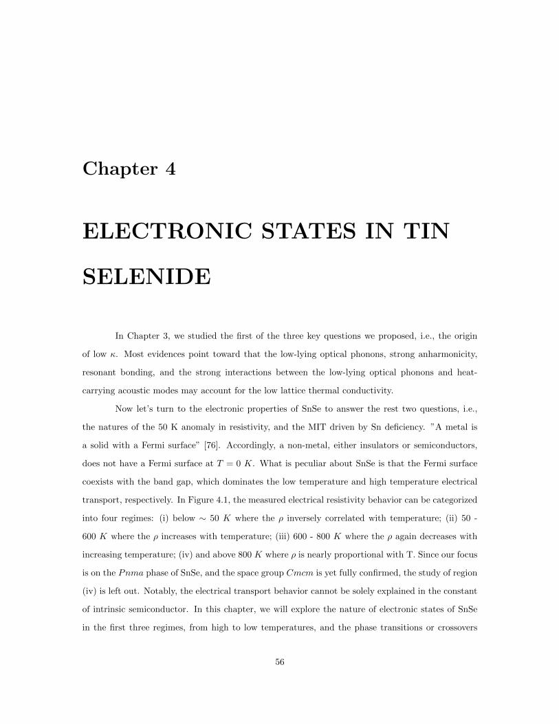
Chapter 4
ELECTRONIC STATES IN TIN
SELENIDE
In Chapter 3, we studied the first of the three key questions we proposed, i.e., the origin
of low κ. Most evidences point toward that the low-lying optical phonons, strong anharmonicity,
resonant bonding, and the strong interactions between the low-lying optical phonons and heat-
carrying acoustic modes may account for the low lattice thermal conductivity.
Now let’s turn to the electronic properties of SnSe to answer the rest two questions, i.e.,
the natures of the 50 K anomaly in resistivity, and the MIT driven by Sn deficiency. ”A metal is
a solid with a Fermi surface” [76]. Accordingly, a non-metal, either insulators or semiconductors,
does not have a Fermi surface at T = 0 K. What is peculiar about SnSe is that the Fermi surface
coexists with the band gap, which dominates the low temperature and high temperature electrical
transport, respectively. In Figure 4.1, the measured electrical resistivity behavior can be categorized
into four regimes: (i) below ∼ 50 K where the ρ inversely correlated with temperature; (ii) 50 -
600 K where the ρ increases with temperature; (iii) 600 - 800 K where the ρ again decreases with
increasing temperature; (iv) and above 800 K where ρ is nearly proportional with T. Since our focus
is on the Pnma phase of SnSe, and the space group Cmcm is yet fully confirmed, the study of region
(iv) is left out. Notably, the electrical transport behavior cannot be solely explained in the constant
of intrinsic semiconductor. In this chapter, we will explore the nature of electronic states of SnSe
in the first three regimes, from high to low temperatures, and the phase transitions or crossovers
56

Figure 4.1: Four regions with different temperature dependence of electrical resistivity and Seebeckcoefficient.
between them by means of the electrical resistivity, Seebeck coefficient, Hall coefficient, magnetic
susceptibility, and specific heat measurements. Note that the X-ray diffraction measurements and
specific heat measurements have confirmed no structural change across those three regions, thus the
term ”phase” merely indicates the electronic (conduction) states in SnSe.
4.1 Density Functional Theory (DFT) Calculations on Elec-
tronic Band Structure of SnSe
DFT calculations were performed to derive the electronic band structure of SnSe. The
calculations were conducted by Drs. Cheng-Rong Hsing and Ching-Ming Wei in Taiwan. Part of
the results are checked by us using the Palmetto Cluster. Since we’re focusing on the Pnma phase,
the calculation of the high temperature Cmcm phase is not discussed here. Figure 4.2 shows both
the calculated total and projected electronic band structure, at different temperatures. The lattice
parameters used at different temperatures are based on the synchrotron XRD measurements. Some
interesting features can be found from the results:
(1) The Fermi level crosses the valence band in Γ − Z direction, forms a small but finite
Fermi surface. In Γ−Y region, the electronic band barely touches the Fermi level. But along Γ−X,
both conduction and valence bands are far away from it.
(2) Among the four valence electron orbitals (s and p bands from both Sn and Se elements),
Se p orbitals account for most of the valence bands that are closest to Fermi level, with Sn s orbitals
57

contributing most of the rest. Sn p orbitals forms most of the conduction bands. And the energy Se
s orbitals are several eV lower than the Fermi level, thus its contribution to electronic conduction is
negligible.
(3) Along Γ − Z, a noticeable deformation of the valence band that crosses EF can be
observed. Essentially, as temperature decreases, the highest point splits into two peaks, forming a
valley-shaped structure.
The projected electronic density of states (DOS) is plotted in Figure 4.3. A distinct hump
of DOS can be found right below Fermi level, which are dominated by Se p orbitals, with some
contribution from Sn s states. The ratio between Se p and Sn s is about 3:1 to 4:1. This result
resembles the situation in PbTe [77], where Te p-states and Pb s-states account for most of the DOS
peak below EF .
There are a few previous works on the electronic band structure calculations of SnSe [36–38],
and our data agrees with their results. Regarding the twin-peak (”pudding-mold-like”) band along
Γ − Z, similar behavior was reported by Shi et al. [36], but not in the work of Guo et al. [38].
The discrepancy probably comes from the different lattice constant used in those two works. In
fact, comparing with the results from our temperature dependent synchrotron XRD measurement,
the lattice constant in Guo’s work is close to the high temperature data (∼ 650 K), and no peak
splitting was observed, whereas the one used by Shi et al. is similar to the value at ∼ 100 K, and
the dual-peak structure was emerged. Therefore, the detailed band structure of SnSe near EF along
Γ−Z is intimately related to the size of the unit cell. And since SnSe is strongly anharmonic and the
lattice constant significantly depends on temperature, it is expected that the temperature change
also has a great impact on its electronic band structure. The twin-peak (”pudding-mold-like”) band
is believed to render a large Seebeck coefficient, as suggested by Kuroki et al. for NaxCoO2 [78].
Thus, it may help explain the large Seebeck coefficient observed in SnSe.
4.2 Experimental Results
4.2.1 Hall Measurements
The carrier scattering mechanism is of fundamental importance is the electrical study of
SnSe. In particular, the temperature dependent carrier mobility µ(T ) calculated from the measured
Hall coefficient RH(T ) and the electrical resistivity ρ(T ) in the relation of µ(T ) = RH(T )/ρ(T ) allow
58

Figure 4.2: Electronic band structure of SnSe at different temperatures using DFT calculations.Calculated by Drs. Cheng-Rong Hsing and Ching-Ming Wei in Taiwan (unpublished).
Figure 4.3: Projected electronic density of states in SnSe.
59

us to study the carrier scattering mechanisms on the microscopic level. Hall coefficients below room
temperature was measured on a Quantum Design® PPMS by sweeping the magnetic field between
+/ − 2 Tesla at each measurement temperature. The effective carrier concentration n is estimated
by the simple formula n = 1/eRH , where e is the elemental charge. As shown in Figure 4.4, the
carrier concentration along three-directions is almost constant above ∼ 75 K. Below 50 K, there
is an increase in n along b and c as temperature decreases, but a drop along a-axis. Similarly, the
mobility in a-axis behaves quite different from that in b- and c-axes when temperature is below
50 K. Above that temperature, all three axes have a power-law mobility. The results in this work
is consistent with the high temperature data reported the Zhao et al. [32].
It is worth noting that the carrier concentration is a scalar, and when we estimated the
carrier concentration from the measured Hall coefficient, the derived carrier concentration is still a
scalar. The observed different carrier concentrations along different crystallographic directions reflect
the nature of multiple-band conduction in SnSe. In the case of multiple band conduction, the derived
carrier concentration is weighted by the mobility of each contributing band. Since the mobility is
a tensor, the derived carrier concentration is thus directional. In this case, it is more appropriate
to call the derived carrier concentration ”effective carrier concentration”. The anisotropy of carrier
concentration reflects the anisotropy of Fermi surface in SnSe. And we can see that as temperature
decreases below ∼ 50 K, the effective charge carriers mainly conduct in the bc plane, whereas in the
out-of-plane direction (a-axis) the carrier concentration rapidly drops.
The temperature dependence of carrier concentration indicates that SnSe has a small but
robust Fermi surface over a wide temperature range. And from the mobility data we can tell
the dominant scattering mechanisms below and above ∼ 50 K: mobility due to acoustic phonon
scattering will have a T−3/2 dependence; optical phonon scattering gives a T−1/2 trend; and charged
defects scattering has a mobility of T 3/2. Hence, we can see that phonon scattering predominates
at temperatures greater than 50 K, but the scattering mechanism below 50 K needs further study.
4.2.2 Sommerfeld Coefficient from Fitting of Specific Heat
Another interesting feature can be found in the fitted specific heat data, as discussed in
the previous chapter. The fitted Sommerfeld coefficient is about ∼ 0.0465 mJ/mol · K2, which is
extremely low. Intuitively, one may assume it implies a null Fermi surface in SnSe. However, the
low Sommerfeld coefficient is also consistent with the low carrier concentration calculated from Hall
60

Figure 4.4: Carrier mobility of SnSe along three axes. Inset: carrier concentration.
61
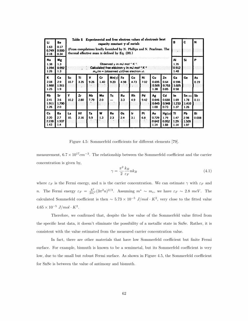
Figure 4.5: Sommerfeld coefficients for different elements [79].
measurement, 6.7× 1017cm−3. The relationship between the Sommerfeld coefficient and the carrier
concentration is given by,
γ =π2
2
kBεFnkB (4.1)
where εF is the Fermi energy, and n is the carrier concentration. We can estimate γ with εF and
n. The Fermi energy εF = h2
2m∗ (3π2n)2/3. Assuming m∗ ∼ me, we have εF ∼ 2.8 meV . The
calculated Sommefeld coefficient is then ∼ 5.73 × 10⁻⁵ J/mol · K2, very close to the fitted value
4.65× 10⁻⁵ J/mol ·K2.
Therefore, we confirmed that, despite the low value of the Sommerfeld value fitted from
the specific heat data, it doesn’t eliminate the possibility of a metallic state in SnSe. Rather, it is
consistent with the value estimated from the measured carrier concentration value.
In fact, there are other materials that have low Sommerfeld coefficient but finite Fermi
surface. For example, bismuth is known to be a semimetal, but its Sommerfeld coefficient is very
low, due to the small but robust Fermi surface. As shown in Figure 4.5, the Sommerfeld coefficient
for SnSe is between the value of antimony and bismuth.
62
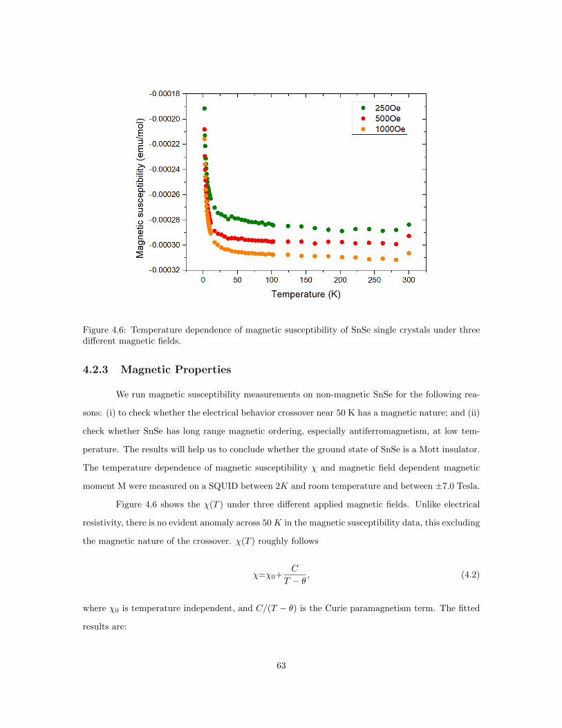
Figure 4.6: Temperature dependence of magnetic susceptibility of SnSe single crystals under threedifferent magnetic fields.
4.2.3 Magnetic Properties
We run magnetic susceptibility measurements on non-magnetic SnSe for the following rea-
sons: (i) to check whether the electrical behavior crossover near 50 K has a magnetic nature; and (ii)
check whether SnSe has long range magnetic ordering, especially antiferromagnetism, at low tem-
perature. The results will help us to conclude whether the ground state of SnSe is a Mott insulator.
The temperature dependence of magnetic susceptibility χ and magnetic field dependent magnetic
moment M were measured on a SQUID between 2K and room temperature and between ±7.0 Tesla.
Figure 4.6 shows the χ(T ) under three different applied magnetic fields. Unlike electrical
resistivity, there is no evident anomaly across 50 K in the magnetic susceptibility data, this excluding
the magnetic nature of the crossover. χ(T ) roughly follows
χ=χ0+C
T − θ, (4.2)
where χ0 is temperature independent, and C/(T − θ) is the Curie paramagnetism term. The fitted
results are:
63
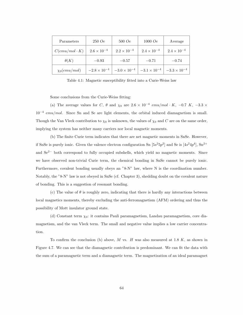
Parameters 250 Oe 500 Oe 1000 Oe Average
C(emu/mol ·K) 2.6× 10⁻⁴ 2.2× 10⁻⁴ 2.4× 10⁻⁴ 2.4× 10⁻⁴
θ(K) −0.93 −0.57 −0.71 −0.74
χ0(emu/mol) −2.8× 10⁻⁴ −3.0× 10⁻⁴ −3.1× 10⁻⁴ −3.3× 10⁻⁴
Table 4.1: Magnetic susceptibility fitted into a Curie-Weiss law
Some conclusions from the Curie-Weiss fitting:
(a) The average values for C, θ and χ0 are 2.6 × 10⁻⁴ emu/mol · K, −0.7 K, −3.3 ×
10−4 emu/mol. Since Sn and Se are light elements, the orbital induced diamagnetism is small.
Though the Van Vleck contribution to χ0 is unknown, the values of χ0 and C are on the same order,
implying the system has neither many carriers nor local magnetic moments.
(b) The finite Curie term indicates that there are net magnetic moments in SnSe. However,
if SnSe is purely ionic. Given the valence electron configuration Sn [5s25p2] and Se is [4s24p4], Sn2+
and Se2− both correspond to fully occupied subshells, which yield no magnetic moments. Since
we have observed non-trivial Curie term, the chemical bonding in SnSe cannot be purely ionic.
Furthermore, covalent bonding usually obeys an ”8-N” law, where N is the coordination number.
Notably, the ”8-N” law is not obeyed in SnSe (cf. Chapter 3), shedding doubt on the covalent nature
of bonding. This is a suggestion of resonant bonding.
(c) The value of θ is roughly zero, indicating that there is hardly any interactions between
local magnetics moments, thereby excluding the anti-ferromagnetism (AFM) ordering and thus the
possibility of Mott insulator ground state.
(d) Constant term χ0: it contains Pauli paramagnetism, Landau paramagnetism, core dia-
magnetism, and the van Vleck term. The small and negative value implies a low carrier concentra-
tion.
To confirm the conclusion (b) above, M vs. H was also measured at 1.8 K, as shown in
Figure 4.7. We can see that the diamagnetic contribution is predominant. We can fit the data with
the sum of a paramagnetic term and a diamagnetic term. The magnetization of an ideal paramagnet
64

follows the Brillouin function [80]
BJ (x) =2J + 1
2Jcoth
(2J + 1
2Jx
)− 1
2Jcoth
(1
2Jx
), (4.3)
where x is a real variable and J is a positive integer/half-integer.
Fitting the M vs. H data with
M = xMBrillouin + yMDM , (4.4)
we have: J ∼ 1.2, x ∼ 0.0016, and y ∼ 0.0038. The fitting curves are also shown in Figure 4.7.
Since an unpaired p-electron has J = 1.5, and s-electron has J = 0.5, a value of 1.2 indicates the
orbitals that unpaired electrons occupy may be a hybridized s-p orbital. This is consistent with the
facts that: (i) The projected electronic density of states indicates the main contribution to charge
carriers are Se-p and Sn-s orbitals, and the ratio between them is about 3 : 1 to 4 : 1; (ii) we have
seen in Chapter 3 that the resonant bonding possibly originates from seven Sn-Se bonds, and both
s- and p-electrons contribute to those bonds. Thus, the J value we obtained is very reasonable.
4.3 Regime (iii): ∼ 600 K - ∼ 800 K
The results of Hall coefficient, Sommerfeld coefficient, and magnetic measurements allow us
to inspect the electrical behavior in different temperature regimes, from high temperature to low
temperature. As shown in Figure 4.1, the temperature dependence of electrical resistivity exhibits a
hump around 600 K, above which it decreases drastically with increasing temperature till ∼ 800 K,
i.e., the transition temperature between Pnma and Cmcm phases. Similarly, the Seebeck coefficient
also shows a negative slope over the temperature range. Therefore, as temperature increases from
600 K to 800 K, SnSe becomes more electrically conductive yet its Seebeck coefficient is getting
lower, typical of a non-degenerate semiconductor.
This phenomenon can be explained by a bipolar effect. At low temperatures, the holes
in SnSe are predominant in charge transport. As temperature goes higher, the energy of thermal
excitation kBT is comparable to the size of the band gap. Hence electrons also play a role in
transport, leading to a Seebeck coefficient hump. Furthermore, the Seebeck coefficient maximum
that characterizes the bipolar effect can be used to quantitatively approximate the band gap of SnSe,
65
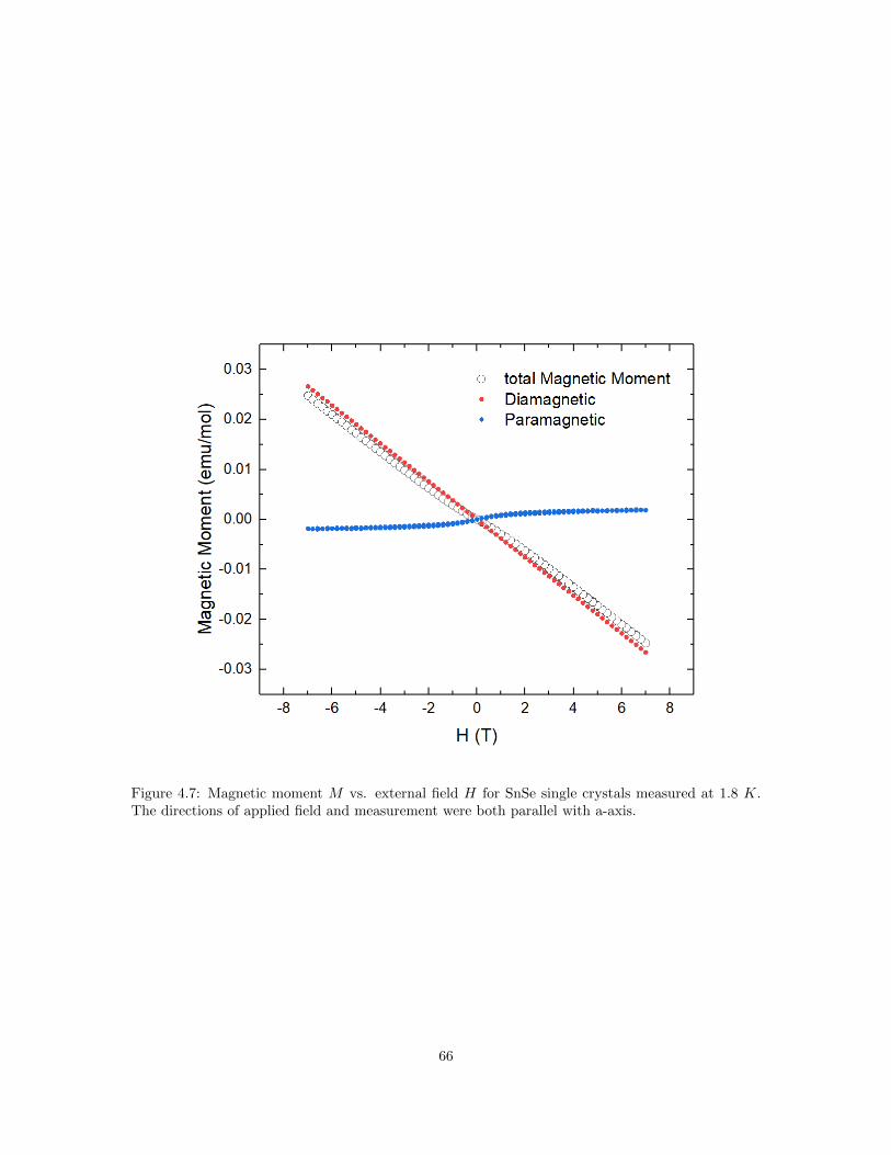
Figure 4.7: Magnetic moment M vs. external field H for SnSe single crystals measured at 1.8 K.The directions of applied field and measurement were both parallel with a-axis.
66

according to Goldsmid-Sharp relation,
Eg = 2e|α|maxTmax. (4.5)
The band gap size Eg is proportional to the product of the max Seebeck coefficient and the cor-
responding temperature. For SnSe, αmax ∼ 550 µV/K, Tmax ∼ 600 K, thus the band gap size
estimated by Goldsmid-Sharp relation is Eg ∼ 0.66 eV , which is lower but comparable to the value
calculated by DFT (Figure 4.3). Note that Goldsmid-Sharp relation is merely an approximation of
the band gap, and it fails in many materials.
From the discussion above, we may attribute the electronic properties of SnSe from ∼ 600 K
to ∼ 800 K to a typical bipolar effect, where both types of charge carriers are conducting. Hence in
this temperature regime SnSe behaves as a typical semiconductor.
4.4 Regime (ii): ∼ 50 K - ∼ 600 K
In light of the semiconducting behavior between 600 K and 800 K, and no phase transition
at 600 K, it is a surprise to see both electrical resistivity and Seebeck coefficient show a positive
temperature dependence, consistent with a metallic or degenerate semiconductor behavior. Since
the Seebeck coefficient is positive over the whole temperature range, the holes are the predominant
charge carriers. The metallic behavior in this region is also consistent with the Hall measurement
and the fitted Sommerfeld coefficient. But this is counterintuitive to the semiconducting nature of
SnSe that has been widely accepted and the semiconducting behavior between 600 K and 800 K.
In fact, there is a controversy on the electrical conduction mechanism in SnSe. Below 600 K, some
groups reported metallic behavior [32, 81, 82], whereas some reported insulating behavior [34, 83],
others reported a nearly temperature independent resistivity [45]. An early work by Yu et al. in
early 1980s [84] showed that where single crystalline SnSe samples grown by the vapor-transport
technique exhibited room temperature carrier concentration and mobility ∼ 9.7 × 1017 cm−3 and
154 cm2/V , respectively. These values are very close to that in our work. Moreover, a similar
metallic behavior was observed below room temperature, as shown in Figure 4.8. Although no MIT
was found around 50 K, a notable drop in the carrier concentration was also observed. The overall
result is consistent with this work, i.e., the SnSe crystals in this work clearly follows a metallic trend
67

Figure 4.8: Electrical Resistivity and carrier concentration reported by Yu et al. in 1981. Replottedfrom Ref. [84].
between 50 and 600 K, and the Hall measurement indicates a finite Fermi surface. The small but
robust Fermi surface at low temperatures contributes about ∼ 1017 cm−3 carrier concentration. This
is far lower than the carrier concentration at ∼ 850 K, which is on the order of 1019 cm−3. Hence,
in view of carrier concentration, the small but robust Fermi surface that leads to the metallic state
from ∼ 50 K to ∼ 600 K is trivial to the highest thermoelectric performance in SnSe.
Shi et al. calculated the topology of Fermi surface with different Fermi energies in the
valence band [36]. For low carrier concentration SnSe, (e.g., Figure 4.9 (b)), the Fermi surface
consists of 2 − 4 small pockets, located in Γ− Y direction. This agrees with the fact that a-axis is
the most insulating direction.
One possible origin of the Fermi surface is the existence of Sn deficiency. SnSe is known
to have a Sn deficiency tendency during crystal growth process, as suggested by Duvjir et al. [85].
In this work, additional Sn was added during the growth process to compensate the loss, but Sn
vacancy still exist in the crystals. We can estimate the amount of Sn vacancies from the measured
carrier concentration.
Assuming all 6.7 × 1017 cm−3 holes are due to Sn vacancies, with the lattice parameters
1.15× 4.17× 4.46 nm3, only one Sn vacancy in about 15000 unit cells is sufficient to generate such
68

Figure 4.9: Calculated Fermi surface with different Fermi energies, with (b) 10 meV , (c) 50 meVand (d) 100 meV [36].
Table 4.2: Estimated mean distance between defects in SnSe, using the Scherrer equation.
T(K)(h00) (0kl) (00l)
(400) (800) (011) (020) (022) (002)65 29 nm 26 nm 24 nm 17 nm 15 nm 14 nm300 28 nm 25 nm 19 nm 29 nm 18 nm 10 nm
a low carrier concentration. This is far lower than the limitation of most techniques. Although we
cannot eliminate the possibility of the small amount of SnSe vacancies, it is intriguing that such
trace amount of deficiency can significantly affect the electrical properties of the material.
The disorder could also be captured by the peak width of XRD pattern. According to
Scherrer equation [86], the average distance between two defects can be expressed as
τ=Kλ
β cos θ. (4.6)
Here K is a dimensionless shape factor; λ is the wavelength of the X-ray; β refers to full-width-half-
maximum (FWHM) and is the Bragg angle.
With K = 0.9 and λ = 0.062 nm, we could estimate τ . Table 4.2 shows the estimated
result. Note here the values are the lowerlimit, because the measured value of FWHM is the sum of
the actual FWHM and the broadening of the instrumental line. So the true mean distance between
defects is higher than that shown in the table. Nonetheless, we could see that τ is about 100 times
larger than the unit cell, and the volume is 5300 nm3. Assuming all defects that broaden the X-ray
peaks are due to Sn2+ vacancies, we get a carrier concentration of ∼ 3 − 4 × 1017 cm−3, which is
within the same order of magnitude of the carrier concentration estimated with Hall measurement
6.7 × 1017 cm−3. Thus, if Sn vacancies explains both the carrier concentration and X-ray peaks
broadening, there needs only a trace amount of them.
69

Figure 4.10: Left: Mossbauer spectroscopy of SnSe crystals in this work, measured in Oak RidgeNational Lab by Dr. Raphael Hermann. Right: Mossbauer spectroscopy of SnSe2, from Ref. [87].
Could the metallic behavior be due to secondary phase? To probe secondary phases, several
experiments were conducted. X-ray diffraction pattern gives no discernible secondary phases. Also,
the results of Mossbauer spectroscopy (Figure 4.10) show that there is no discernible SnSe2 peak and
the off-stoichiometry is no higher than 0.5%, confirming the purity of our SnSe crystals. Note here a
Se-rich crystal is also prepared and measured, and no SnSe2 was found by Mossbauer measurements
either.
4.5 Regime (i): Below 50 K
Surprisingly, the electrical resistivity undergoes another crossover around ∼ 50 K, exhibit-
ing a non-metallic behavior. In most band conductors, such resistivity behavior is caused by thermal
excitation across the band gap. By contrast, the Seebeck coefficient doesn’t show any discernable
feature near 50 K. More importantly, the Seebeck coefficient follows a metal or degenerate semi-
conductor behavior, following the Pisarenko relation,
α =8π2kB
2T
2qh2m∗( π
3n
)2/3
. (4.7)
We can estimate the Seebeck coefficient in SnSe using Pisarenko relation, using 0.5me and 0.15me
as the effective masses in a and c directions, respectively. These values are chosen according to the
70

Figure 4.11: Comparison of measured Seebeck coefficients and estimated values using the Pisarenkorelation (gray dashed lines).
theoretical calculations [38].
As shown in Figure 4.11, the measured Seebeck coefficient agrees well with our estimation
at low temperatures. Hence, the electronic state in SnSe below 50 K can be attributed to a metallic
or degenerate semiconductor behavior. Below 50 K, the measured carrier concentration from Hall
measurements indicates a finite amount of charge carriers (holes) persists till ∼ 0 K, contradictory
to the non-metallic resistivity behavior observed. And as mentioned before, the temperature depen-
dence of magnetic susceptibility doesn’t show a discernible anomaly around 50 K. Here we try to
understand the 50 K resistivity anomaly using to scenarios: band conduction and variable range
hopping.
4.5.1 Band Conduction
If the resistivity upturn below 50 K in a-axis can be fitted to a semiconducting behavior.
Ideally, the electrical conductivity of an insulator/semiconductor follows,
σ = σ0e− Eg
2kBT , (4.8)
71

Figure 4.12: lnσ vs. 1/T for temperatures below 50 K.
which can be written as,
lnσ = − Eg2kB
1
T+ lnσ0, (4.9)
i.e., lnσ is proportional to 1/T , and the slope is proportional to the bandgap.
Figure 4.12 shows the results for T < 50 K. We can see that lnσ roughly follows a linear
relationship with temperature only along a-direction. The fitted slope in that direction is −6.07.
That is to say, if the insulating state of SnSe below 50 K is due to a newly opened band gap, the
value of the band gap is only around the energy of 12 K, which is merely ∼ 1 meV . This is also
hard to reconcile with the ∼ 1 eV band gap of SnSe. Therefore, we exclude the band gap as the
origin of the non-metallic state. In the other two primary crystallographic directions, the resistivity
upturn is barely seen: the slope is practically zero.
72

Figure 4.13: (a) ln(σ) and (b) Seebeck coefficient as a function of T−1/4. The black solid linesindicate variable range hopping fitting.
4.5.2 Variable Range Hopping
Another possible scenario is variable range hopping (VRH). VRH describes the conduction
in strongly localized systems at low temperatures. Rather than band conduction, charge carriers are
hopping between different sites for conduction. The hopping probability depends on spatial distance
and energy difference between two sites. Mott pointed out that in such a system, the electrical
conductivity and Seebeck coefficient follows [88]
σ = σ0e−(T0
T )1
d+1
, (4.10)
α = α0T1
d+1 . (4.11)
Here T0 is a constant, and d denotes the dimensionality of the system. Figure 4.13 shows the fitted
results for d = 3. The fitting is much better comparing with the band conduction scenario, although
there is still some deviation in b-axis. We can see that VRH model explains the electrical resistivity
behavior very well. Moreover, the Seebeck coefficient roughly follows VRH model as well. Thus, we
may attribute the insulating state to localization effect. We will discuss the possible origin of the
localization in the following.
73

Figure 4.14: Resistivity vs. Seebeck coefficient plot of SnSe.
4.5.3 Explanation with Localization
If the resistivity upturn below 50 K is due to localization, the localization is anisotropic:
strong in a-direction but hardly seen in other two directions. Now let’s look into what drives the
metal-insulator-transition (MIT). The 55 K crossover can be more easily seen if we plot resistivity
vs. Seebeck coefficient (Figure 4.14).
To investigate the transition around 50 K, we will first introduce several most common
mechanisms of MIT (Figure 4.15). Then to find out which one applies to SnSe, density functional
theory (DFT) calculations were conducted in conjunction with In doping to pinpoint the driving
force underlying the 50 K crossover.
A metal-insulator transition (MIT) is one of the most fundamental yet least understood
topics in physics. It has been observed in numerous materials, but to a lot of them the driving
forces are still unclear. Basically, there are at least three types of mechanisms that lead to MIT:
electronic band gap, interaction between electrons, and interaction between electron and disorder.
Among them the MIT due to band gap is the most well understood, thanks to the development
of the band theory. MIT that resulted from electron-electron interaction is also known as Mott
insulator. If the coupling between electrons are strong enough, the energy cost of electron transfer
74

Figure 4.15: The categories of metal to insulator transition (MIT).
is so large that the system is insulating even if the conduction band is partially filled. The third
type of MIT is driven by the presence of disorder in the system, such as impurity atoms. It has
been proven by P.W. Anderson in 1958 that [89], for low dimensional systems (1D or 2D), any
degree of randomness (disorder) will localize the electrons, making the system insulating. And for
3D materials, the electrons are completely localized if the disorder in the lattice is sufficiently large.
Weak localization, which results from the interference of the random walk paths, can be treated as a
precursor of Anderson localization. In real materials, the latter two types of insulators are difficult
to detect and distinguish directly.
What would be the case for the MIT in SnSe at ∼ 50 K? Although theoretically, SnSe is a
semiconductor with a finite band gap, the carrier concentration measured in this work indicates a
finite Fermi surface along b and c directions, even near 0 K. Therefore, we may exclude the band
gap insulating as the origin of the MIT for those two directions. For a-axis, further investigations
are needed.
As for Mott insulators, an equation called Mott criterion states that nc(1/3)aH
∗ = 0.26 is
a critical relationship that determines Mott insulator. Here nc is the critical carrier concentration,
while aH∗ is the Bohr radius [90]. For doped semiconductors, they become metallic when the carrier
concentration exceeds the critical value nc, as shown in Figure 4.16. Siegrist et al. suggested that
GeSb2Te4 is far away from the Mott criterion, so it is not a Mott insulator [91]. For SnSe, since it
is strongly anisotropic, the Bohr radius is quite different in three directions (29, 164,148 A for a, b,
75
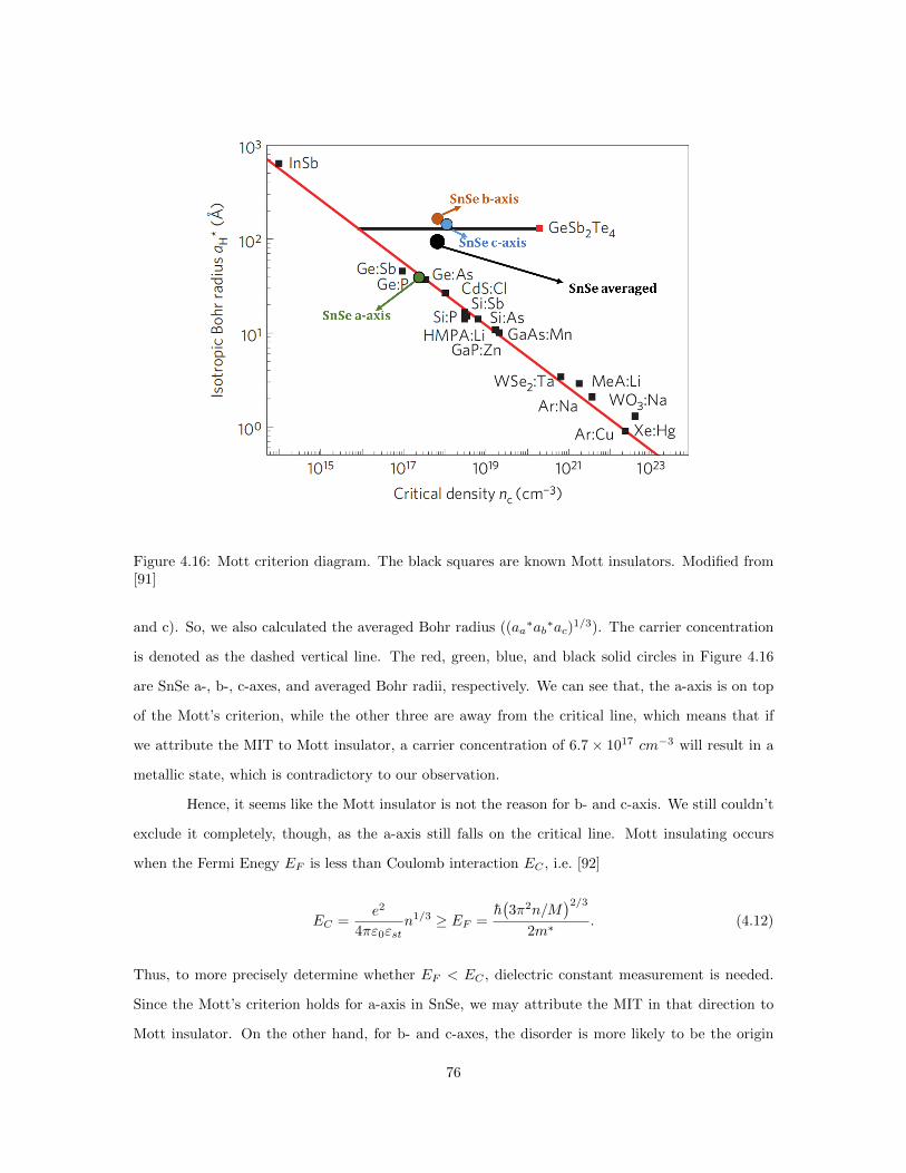
Figure 4.16: Mott criterion diagram. The black squares are known Mott insulators. Modified from[91]
and c). So, we also calculated the averaged Bohr radius ((aa∗ab∗ac)
1/3). The carrier concentration
is denoted as the dashed vertical line. The red, green, blue, and black solid circles in Figure 4.16
are SnSe a-, b-, c-axes, and averaged Bohr radii, respectively. We can see that, the a-axis is on top
of the Mott’s criterion, while the other three are away from the critical line, which means that if
we attribute the MIT to Mott insulator, a carrier concentration of 6.7× 1017 cm−3 will result in a
metallic state, which is contradictory to our observation.
Hence, it seems like the Mott insulator is not the reason for b- and c-axis. We still couldn’t
exclude it completely, though, as the a-axis still falls on the critical line. Mott insulating occurs
when the Fermi Enegy EF is less than Coulomb interaction EC , i.e. [92]
EC =e2
4πε0εstn1/3 ≥ EF =
h(3π2n/M
)2/32m∗
. (4.12)
Thus, to more precisely determine whether EF < EC , dielectric constant measurement is needed.
Since the Mott’s criterion holds for a-axis in SnSe, we may attribute the MIT in that direction to
Mott insulator. On the other hand, for b- and c-axes, the disorder is more likely to be the origin
76
of MIT, i.e., the MIT in SnSe along b and c is more likely due to Anderson localization than Mott
insulator.
We have seen that, the magnetic susceptibility (cf. Figure 4.6) indicates not antiferromag-
netic (AFM) transition occurred in SnSe down to 2 K, a signature of a Mott insulator. Ideally, a
Mott insulator would be AFM, because electrons near EF are confined on local sites due to the fact
that the intra-site transfer integral is weaker than the strength of inter-site Coulomb interaction.
Therefore, the magnetic susceptibility measurement implies Mott insulating does not apply to SnSe.
Hence, the MIT along a-axis is more complicated than that along b and c, and more experiments
and theoretical calculations are needed.
Regarding Anderson localization, what type of disorder would it be that induces MIT along b
and c, considering we have almost perfect single crystallinity? The most likely disorder is still the Sn
vacancies, even though there is only a tiny amount. But why is SnSe metallic above 50 K? Although
point defects are almost independent on temperature, but Fermi level can still move with temperature
change, via (a) population more charge carriers according to Fermi-Dirac distribution; (b) lattice
distortion with temperature change alters electronic band structure; (c) electronic band structure
change due to lattice expansion/compaction. As shown in the DFT calculated electronic band
structure of SnSe (cf. Figure 4.2), the Fermi level cross more valence band as temperature increases.
Although the calculations are based on lattice constants measured at different temperatures above
50 K, we may still assume that 50 K is a critical temperature where Fermi energy EF is roughly
equal to the mobility edge Eµ. Below 50 K, EF < Eµ, results in an insulating state. The shift in
EF was confirmed by the ARPES result reported recently [93]. Figure 4.17 is a schematic of the
electronic states as temperature changes.
4.5.4 Explanation with Electronic Band Structure
Another explanation of the anomaly is by the change in electronic band structure, which
increase in the effective mass of holes at low temperatures. Firstly, as seen in Figure 4.11, the
effective mass of holes indeed increases along a- and c-axes as temperature decreases below 50 K.
In fact, this enhancement in effective mass was confirmed by a recent angle-resolved photoemission
spectroscopy (ARPES) work by Lu et al. [93]. As shown in Figure 4.18, a significant enhancement
in effective mass can be observed for electronic band along Γ − Z direction, and along Γ − Y the
effective mass is slightly increased. Thus, the upturn in resistivity can be explained by the fact that
77

Figure 4.17: Schematic of the change in EF with temperature increases.
the effective mass of carriers increases as temperature goes to zero.
But why is there an enhancement in effective mass? The temperature evolution of electronic
band structure illustrated in Figure 4.2 may be the reason. At high temperatures, the band along
Γ− Z adopts a single parabolic shape. As temperature decreases, an extra valence band maximum
(VBM) appears, forming an M-shaped band structure. As mentioned at the beginning of this
chapter, this M-shaped band structure is called Pudding −Mold , and has been shown to have a
high effective mass. The large effective mass explains the upturn in electrical resistivity.
Therefore, the anomaly around 50 K could also be explained by the change in electronic
band structure as temperature changes. Comparing with the localization model, we suggest this
model would be morelikely to be the reason of the anomaly around 50 K.
4.6 Probe Localization via Doping Study
As mentioned in last section, one possible explanation of the metallic behavior is due to
the existence of Sn vacancies. We have conducted several experiments, and shown that even there
are Sn vacancies, the content is less than one per 15000 unit cells. Thus, we could still claim that
78

Figure 4.18: Temperature evolution for the ARPES-extracted effective masses of differencebands [93].
79

Figure 4.19: Electrical resistivity vs. temperature for SnSe of different stoichiometry.
SnSe is natively metallic over a wide temperature range. An intuitive question would then be: (i)
what if we intentionally add Sn vacancies, i.e., introducing non-stoichiometry? (ii) How would other
impurities such as dopants affect the electronic properties? In this chapter, we try to answer these
two questions via intentionally introducing two types of impurities: Sn vacancies and indium.
4.6.1 Sn Vancancies
As mentioned in Chapter 2, with more and more Sn vacancies introduced, a naıve thought
would be a more conductive sample, because Sn vacancies make the material more p-type, by
introducing holes into the system. The result, however, is counter-intuitive.
Figure 4.19 shows the temperature dependence of electrical resistivity of Sn0.99Se, and
Sn0.94Se. The stoichiometric SnSe in this work and the result reported by Ibrahim et al. are
also plotted as a comparison. We can see that Sn0.99Se is more conductive than the single crystals
prepared in this work. But as more and more Sn vacancies are introduced, the electrical resistivity
eventually behaves as an insulator! The result reported by Ibrahim et al. [34] sits between Sn0.99Se
and Sn0.94Se, although they did not disclose the composition of their samples.
80
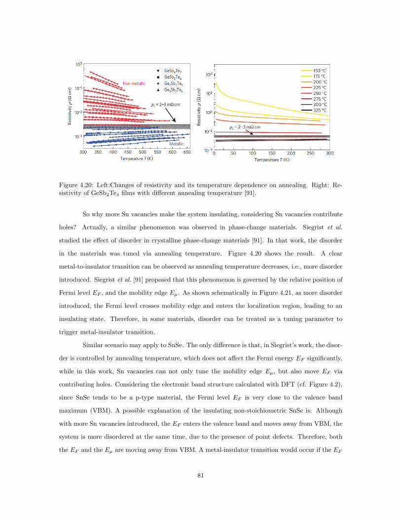
Figure 4.20: Left:Changes of resistivity and its temperature dependence on annealing. Right: Re-sistivity of GeSb2Te4 films with different annealing temperature [91].
So why more Sn vacancies make the system insulating, considering Sn vacancies contribute
holes? Actually, a similar phenomenon was observed in phase-change materials. Siegrist et al.
studied the effect of disorder in crystalline phase-change materials [91]. In that work, the disorder
in the materials was tuned via annealing temperature. Figure 4.20 shows the result. A clear
metal-to-insulator transition can be observed as annealing temperature decreases, i.e., more disorder
introduced. Siegrist et al. [91] proposed that this phenomenon is governed by the relative position of
Fermi level EF , and the mobility edge Eµ. As shown schematically in Figure 4.21, as more disorder
introduced, the Fermi level crosses mobility edge and enters the localization region, leading to an
insulating state. Therefore, in some materials, disorder can be treated as a tuning parameter to
trigger metal-insulator transition.
Similar scenario may apply to SnSe. The only difference is that, in Siegrist’s work, the disor-
der is controlled by annealing temperature, which does not affect the Fermi energy EF significantly,
while in this work, Sn vacancies can not only tune the mobility edge Eµ, but also move EF via
contributing holes. Considering the electronic band structure calculated with DFT (cf. Figure 4.2),
since SnSe tends to be a p-type material, the Fermi level EF is very close to the valence band
maximum (VBM). A possible explanation of the insulating non-stoichiometric SnSe is: Although
with more Sn vacancies introduced, the EF enters the valence band and moves away from VBM, the
system is more disordered at the same time, due to the presence of point defects. Therefore, both
the EF and the Eµ are moving away from VBM. A metal-insulator transition would occur if the EF
81

Figure 4.21: Schematic plot of the metal-insulator transition in some phase-change materials [91].
is between the Eµ and VBM. Figure 4.22 shows schematically the transition. A notable difference
between this model and Figure 4.22 is that the Fermi level is fixed in those phase-change materials,
whereas in the model we proposed for SnSe, both EF and Eµ are moving as Sn vacancies are added,
and the relative position of them determines the electrical behavior the system exhibits.
Of course, there are other models that could lead to the metal-insulator transition. And
further investigation is needed. In fact, SnSe is known to tend to form Sn vacancy. Duvjir et
al. studied the Sn vacancies in SnSe with STM [85]. Figure 4.23 shows the STM result of Sn
vacancy. It was found that Sn vacancies move the EF inside the valence band and produce extra
holes throughout the system, which is consistent with our model.
4.6.2 Indium Doping
Aside from Sn vacancies, In-doped SnSe single crystalline samples were was also prepared.
Substituting Sn with In in SnSe would introduce holes into the system, and since SnSe is natively
p-type, In-doping will enhance electrical conductivity. Surprisingly, all three samples show insu-
lating behavior. However, all three samples prepared are insulating, as shown in the Figure 4.24.
In0.05Sn0.95Se is the most insulating sample over the entire temperature range. This phenomenon
could also be explained by the same model proposed for Sn vacancies case: the point defects in-
troduced by In doping localizes the charge carriers. But here even only 1% of In could lead to an
insulating state. Figure 4.25 shows the ln(σ) vs. T−1/4 plot for all three samples. We can see that
82
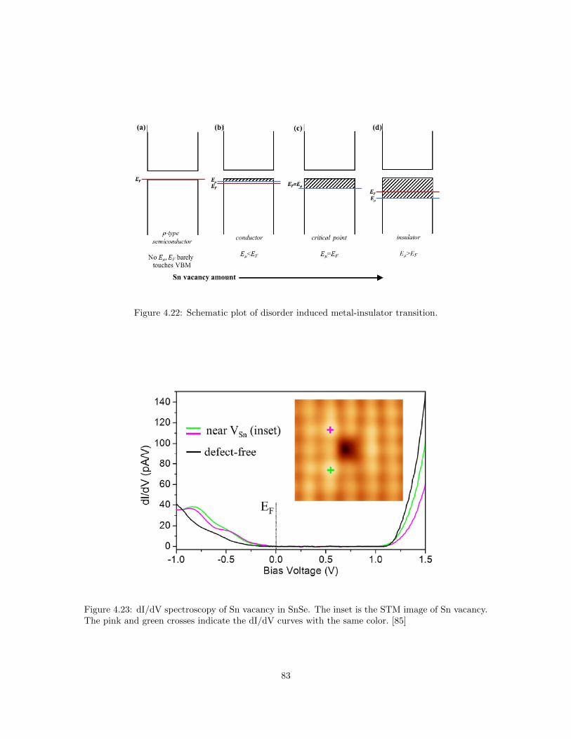
Figure 4.22: Schematic plot of disorder induced metal-insulator transition.
Figure 4.23: dI/dV spectroscopy of Sn vacancy in SnSe. The inset is the STM image of Sn vacancy.The pink and green crosses indicate the dI/dV curves with the same color. [85]
83

Figure 4.24: Electrical resistivity of In-doped SnSe.
all three samples basically follow a linear trend, but with a kink at ∼ 200 K. The linearity supports
the VRH model, but still, more investigations are needed to confirm.
Therefore, it seems like SnSe is on the verge of localization. At low temperatures, Sn
deficiency and In-doping will all localize the charge carrier via Anderson localization. For single
crystalline SnSe, the MIT is controlled by moving the EF with temperature; while for Sn deficiency
and In-doping, the MIT is tuned by the relative position of EF and mobility edge Eµ.
In this chapter, we tried to answer the second and third questions, i.e., the natures of the 50
K anomaly and the MIT driven by Sn vacancies. For the 50 K anomaly, we think it is likely due to
the change in electronic band structure, which forms a pudding −mold shape at low temperatures,
leading to an enhancement in hole effective mass. For the MIT driven by deficiency, it is attributed
to the Anderson localization, which is due to the competition of Fermi energy and mobility edge.
84
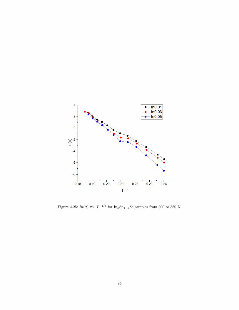
Figure 4.25: ln(σ) vs. T−1/4 for InxSn1−xSe samples from 300 to 850 K.
85

Chapter 5
CONCLUSIONS AND FUTURE
WORKS
In this thesis, we addressed the three primary questions by means of the temperature de-
pendent resistivity, Seebeck coefficient, Hall coefficient, specific heat, thermal conductivity, magnetic
susceptibility and X-ray diffraction measurements in conjunction with density functional theory cal-
culations. These results presented a grand picture how SnSe evolves structurally, electrically, and
thermally from a low temperature metallic state to a high temperature semiconducting state toward
a promising thermoelectric performance. In particular, we found that (i) high quality pristine SnSe
single crystals exhibit a metallic ground state (aka a small but robust Fermi surface with multiple
pockets) with a coexisting band gap; (ii) off stoichiometry and doping could destabilize the Fermi
surface; (iii) the low lying low-lying optical phonon modes, resonant bonding, strong anharmonic-
ity, and strong phonon-phonon interaction contribute to the low lattice thermal conductivity. We
obtained a thermoelectric figure of merit ZT ∼ 1.0, ∼ 0.8 and ∼ 0.25 at 850 K along the b, c and
a directions. We have also discussed the formation of Fermi surface in relation to the Sn vacan-
cies and the disorder induced metal to insulator transition in light of Anderson localization. We
demonstrated that, the MIT could be triggered by defect engineering (both Eµ and EF change).
For the resistiviy anomaly around 50 K, we attribute it to the change in electronic band structure
as temperature decreases.
Some profound questions remained to be answered in SnSe. For example, it should be
86
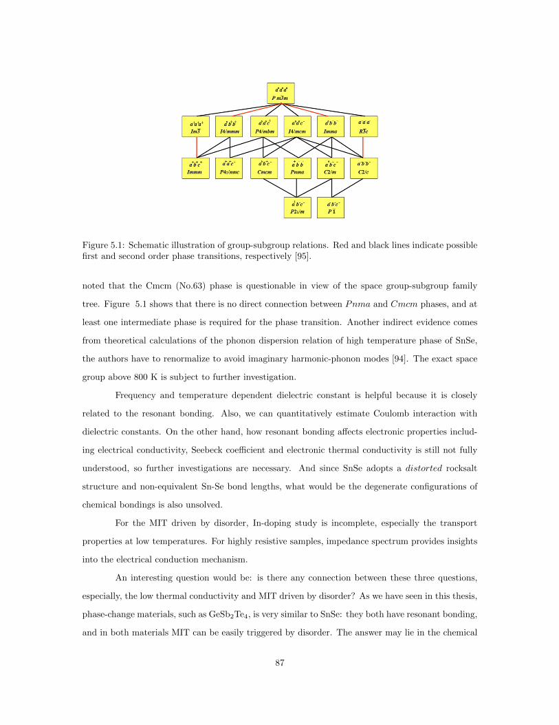
Figure 5.1: Schematic illustration of group-subgroup relations. Red and black lines indicate possiblefirst and second order phase transitions, respectively [95].
noted that the Cmcm (No.63) phase is questionable in view of the space group-subgroup family
tree. Figure 5.1 shows that there is no direct connection between Pnma and Cmcm phases, and at
least one intermediate phase is required for the phase transition. Another indirect evidence comes
from theoretical calculations of the phonon dispersion relation of high temperature phase of SnSe,
the authors have to renormalize to avoid imaginary harmonic-phonon modes [94]. The exact space
group above 800 K is subject to further investigation.
Frequency and temperature dependent dielectric constant is helpful because it is closely
related to the resonant bonding. Also, we can quantitatively estimate Coulomb interaction with
dielectric constants. On the other hand, how resonant bonding affects electronic properties includ-
ing electrical conductivity, Seebeck coefficient and electronic thermal conductivity is still not fully
understood, so further investigations are necessary. And since SnSe adopts a distorted rocksalt
structure and non-equivalent Sn-Se bond lengths, what would be the degenerate configurations of
chemical bondings is also unsolved.
For the MIT driven by disorder, In-doping study is incomplete, especially the transport
properties at low temperatures. For highly resistive samples, impedance spectrum provides insights
into the electrical conduction mechanism.
An interesting question would be: is there any connection between these three questions,
especially, the low thermal conductivity and MIT driven by disorder? As we have seen in this thesis,
phase-change materials, such as GeSb2Te4, is very similar to SnSe: they both have resonant bonding,
and in both materials MIT can be easily triggered by disorder. The answer may lie in the chemical
87

bondings in the materials, and more experiments as well as theoretical studies are necessary.
88

Appendices
89

Appendix A Onsager’s Reciprocal Relations
Onsager’s description provides an in-depth understanding of thermoelectricity from a flow
perspective [16]. Since thermoelectric process is in a non-equilibrium stationary system, from the
laws of energy and matter conservation, the thermoelectric process can be described by the following
expression,
JE = JQ + µeJN . (1)
Here JE , JQ, µe and JN are total energy flux, heat flux, chemical potential of charge carriers, and
total particles flux, respectively. These three fluxes are driven by their corresponding thermodynamic
potentials. In physics, we study these potentials (the causes) by studying the fluxes (the effects). It
can be shown that for the energy and particles fluxes, the corresponding potentials are 1/T and µe/T ,
respectively. Thus the forces that drive the particles and energy fluxes are simply their gradients,
FN = ∇(−µeT
), FE = ∇
(− 1
T
). (2)
Since the energy and particles fluxes are coupled, they can be expressed in a matrix form,
JN
JE
=
LNN LNE
LEN LEE
∇ (−µe/T )
∇ (−1/T )
. (3)
In Onsager description, a system under non-equilibrium conditions minimizes its entropy
production, which leads to the symmetry of the off-diagonal term in the matrix, i.e., LNE = LEN [96].
This is almost the result of time reversal symmetry of the process.
The above expressions can be rewritten in the form of JQ = JE − eJN . Then the matrix
form of the fluxes can be expressed as,
JN
JQ
=
L11 L12
L21 L22
− 1
T∇µe
∇(
1T
) . (4)
Here L12 = L21, and the four L terms have the form
L11 = LNN , (5)
90
L11 = LNE − µeLNN , (6)
L22 = LEE − µe (LEN + LNE) + µe2LNN . (7)
If the system is isothermal, that is, there is no temperature gradient, the electrical current density
J = eJN is solely dependent on the L11 term and the gradient of chemical potential, and takes the
form
J =−eL11
T∇µe. (8)
This is simply Ohm’s law, with conductivity σT = e2
T L11.
On the other hand, if we assume there is no particle transport, i.e., J = −L11
(1T∇µe
)+
L12∇(
1T
)= 0. The heat flux density is then,
JQ =1
T 2
(L21L12 − L11L22
L11
)∇T. (9)
This is Fourier’s law, with thermal conductivity κ = 1T 2 (L21L12−L11L22
L11). Another condition is when
electrochemical gradient is zero. In this scenario, we get thermal conductivity κ = L22
T 2 .
The above discussion considers only the decoupled processes. Another important quantity in
thermoelectricity is the Seebeck coefficient, which describes the coupling between electrochemical and
temperature gradients. Assuming there is no particle transport, the definition of Seebeck coefficient
α is
−1
e∇µe ≡ α∇T = E|J=0, (10)
which can be written as
α =1
eT
L12
L11. (11)
On the other hand, similarly, under isothermal condition, we can derive the expression of
the Peltier coefficient, Π = 1eL12
L11. Therefore, as expected, we obtain =T. Next, we will show that
both theses quantities can be understood as a representation of entropy per carrier, as pointed out
91

by Callen [97]. To clarify this concept, let us first express the entropy flux density,
JS =1
T
[−L21
(1
T∇µe
)+ L22∇
(1
T
)]. (12)
We can plug in the energy flux density J into the above equation,
JS =L21
TeL11J +
1
TL22∇
(1
T
). (13)
This equation indicates that the total entropy flux has two contributions: one from charge
carriers, and the other from thermal transport. For the first term, the coefficient of current density
is nothing but Seebeck coefficient α. Despite the surprisingly simple insight that the Seebeck co-
efficient provides, it is worth noting that entropy per carrier results from an averaged effect of the
current contribution to the total entropy flow. One should not say that the current contribution to
total entropy is the simple summation of individual contribution of all charge carriers, because ther-
modynamics cannot be reduced to a single particle. Again, entropy reflects the number of possible
microstates.
92
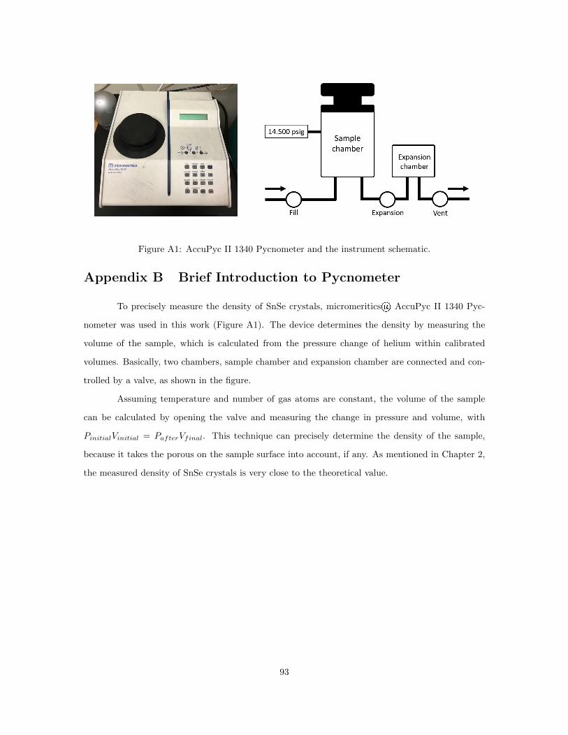
Figure A1: AccuPyc II 1340 Pycnometer and the instrument schematic.
Appendix B Brief Introduction to Pycnometer
To precisely measure the density of SnSe crystals, micromeritics® AccuPyc II 1340 Pyc-
nometer was used in this work (Figure A1). The device determines the density by measuring the
volume of the sample, which is calculated from the pressure change of helium within calibrated
volumes. Basically, two chambers, sample chamber and expansion chamber are connected and con-
trolled by a valve, as shown in the figure.
Assuming temperature and number of gas atoms are constant, the volume of the sample
can be calculated by opening the valve and measuring the change in pressure and volume, with
PinitialVinitial = PafterVfinal. This technique can precisely determine the density of the sample,
because it takes the porous on the sample surface into account, if any. As mentioned in Chapter 2,
the measured density of SnSe crystals is very close to the theoretical value.
93
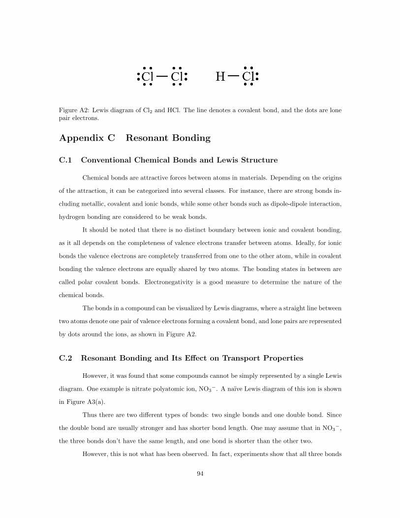
Figure A2: Lewis diagram of Cl2 and HCl. The line denotes a covalent bond, and the dots are lonepair electrons.
Appendix C Resonant Bonding
C.1 Conventional Chemical Bonds and Lewis Structure
Chemical bonds are attractive forces between atoms in materials. Depending on the origins
of the attraction, it can be categorized into several classes. For instance, there are strong bonds in-
cluding metallic, covalent and ionic bonds, while some other bonds such as dipole-dipole interaction,
hydrogen bonding are considered to be weak bonds.
It should be noted that there is no distinct boundary between ionic and covalent bonding,
as it all depends on the completeness of valence electrons transfer between atoms. Ideally, for ionic
bonds the valence electrons are completely transferred from one to the other atom, while in covalent
bonding the valence electrons are equally shared by two atoms. The bonding states in between are
called polar covalent bonds. Electronegativity is a good measure to determine the nature of the
chemical bonds.
The bonds in a compound can be visualized by Lewis diagrams, where a straight line between
two atoms denote one pair of valence electrons forming a covalent bond, and lone pairs are represented
by dots around the ions, as shown in Figure A2.
C.2 Resonant Bonding and Its Effect on Transport Properties
However, it was found that some compounds cannot be simply represented by a single Lewis
diagram. One example is nitrate polyatomic ion, NO3−. A naıve Lewis diagram of this ion is shown
in Figure A3(a).
Thus there are two different types of bonds: two single bonds and one double bond. Since
the double bond are usually stronger and has shorter bond length. One may assume that in NO3−,
the three bonds don’t have the same length, and one bond is shorter than the other two.
However, this is not what has been observed. In fact, experiments show that all three bonds
94

Figure A3: (a)A naıve Lewis diagram of nitrate polyatomic ion NO3−; (b) Three different configu-
rations of NO3− that have the same energy; (c) Lewis-like diagram of NO3
− with resonant bonding
Figure A4: Lewis-like diagram of benzene.
have the same bonding strength. Moreover, it has been shown that the strength and the length are
both between single and double N-O bonds. Therefore, a more complicated model is need to explain
the chemical bonds in NO3−. And the model is known as resonant bonding. Imagine the chemical
bonds in NO3− actually have three different configurations, and they resonate. In each of three
structures, one of the three bonds is double bonding, and the other two are single bonds, as depicted
in Figure A3(b). By adopting such a “resonance” state, the lengths of the three bonds would be
expected to be the same. However, it should be noted that nitrate ion is not really switching between
one structure to another. The actual configuration can be treated as a blend of these three resonance
structures. In order to better describe the actual structure of chemical bonds in nitrate ion, we can
adopt a Lewis-like structure, as shown in Figure A3(c). Here the dotted lines denote the bonds that
exist in at least one but not all the resonance structures.
Another important example of resonance is benzene, which has no lone pairs. It has two
types of C-C bonds, and for convenience, its Lewis-like diagram is shown in Figure A4.
95

Figure A5: Schematic diagram of resonant bonding for Sb. Image taken from ref. [99].
Thus we can see that compounds with resonant bonds are very different from those with
ionic or covalent bonds. In next section we will briefly discuss two classes of materials that have
resonant bonds, and how resonant bonds affect their physical properites.
C.3 Resonant Bonding in Real Materials
Resonant bonding have been intensively studied in a class of materials called phase change
materials (PCM). PCM are solids which can switch between amorphous and crystalline phases
rapidly. The optical properties in these two phases are very different, facilitating the usage of optical
data storage, such as rewritable CDs [98]. One of the most popular PCM is GeSbTe, which is a
composition of GeTe-Sb2Te3. It was found that the difference of optical properties in its amorphous
and crystalline phases could be attributed to the nature of bonding between atoms. Shportko et
al. claimed that amorphous GeSbTe is a covalent semiconductor, whereas its crystalline counterpart
adopts resonant bonding, which significantly enhances the optical dielectric constant [99]. Figure A5
illustrates the resonant bonding for Sb in NaCl structure, which has a similar structure with GeSeTe.
The left and right subplot in Figure A5 are two possible configurations of bonding between Sb atoms,
where each Sb atom has six nearest neighbors, but each Sb only has three p-electrons. Thus those two
configurations are unstable and will undergo a Peierls distortion. But the solid then can minimize
the total energy by hybridizing the electronic wavefunction, forming the resonant bonding shown in
the middle of Figure A5 As now the electrons are highly delocalized, the electronic polarizability is
strongly enhanced. Similar phenomenon was also found for some GeSbTe compounds [98].
Other than PCMs, resonant bonding is also present in many crystalline IV-VI compounds [100].
Similarly, large optical dielectric constants were observed in those materials. Littlewood developed
a diagram to identify the nature of the structure and bonding in IV-VI compounds [101], where two
96
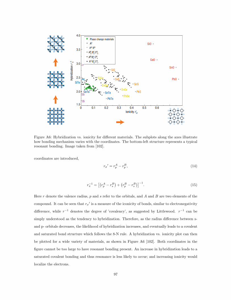
Figure A6: Hybridization vs. ionicity for different materials. The subplots along the axes illustratehow bonding mechanism varies with the coordinates. The bottom-left structure represents a typicalresonant bonding. Image taken from [102].
coordinates are introduced,
rσ′ = rAp − rBp , (14)
r−1π =
[(rAp − rBs
)+(rBp − rBs
)]−1. (15)
Here r denote the valence radius, p and s refer to the orbitals, and A and B are two elements of the
compound. It can be seen that rσ′ is a measure of the iconicity of bonds, similar to electronegativity
difference, while r−1 denotes the degree of ’covalency’, as suggested by Littlewood. r−1 can be
simply understood as the tendency to hybridization. Therefore, as the radius difference between s-
and p- orbitals decreases, the likelihood of hybridization increases, and eventually leads to a covalent
and saturated bond structure which follows the 8-N rule. A hybridization vs. ionicity plot can then
be plotted for a wide variety of materials, as shown in Figure A6 [102]. Both coordinates in the
figure cannot be too large to have resonant bonding present. An increase in hybridization leads to a
saturated covalent bonding and thus resonance is less likely to occur; and increasing ionicity would
localize the electrons.
97
Therefore, as discussed above, resonant bonding materials usually feature a large optical
dielectric constant, i.e., high electronic polarizability. Also, unlike regular electron pair bond of the
8-N rule, where only the nearest neighbors are involved, resonant bonding requires a longer-range
ordering. It is worth noting that the long-range interaction is not from Coulomb interaction, as
pointed out by [70].
There are also single element crystals that adopt resonant bonding, such as Se and Te.
Most of resonant bonding materials found so far have a cubic structure, and have a large dielectric
constant. Also, since resonant bonding requires unsaturated covalent bonds, it cannot occur in
materials with sp3-bonding.
C.4 Effects of Resonant Bonding on Thermoelectric Properties
Resonant bonding is also in favor of thermoelectric applications. Although it is still not clear
how exactly resonant bonding impacts thermoelectric properties (electrical conductivity, Seebeck
coefficient, and thermal conductivity), it is no doubt that a crystal featuring such kind of bonding
will have some intriguing behavior.
Lee et al. studied the effect of resonant bonding on lattice thermal conductivity on some
popular thermoelectric materials [70]. From their first-priciples calculations, it was argued that
in some rocksalt structured materials, such as lead chalcogenides, SnTe, Bi2Te3, Bi and Sb, the
long-ranged interaction along 〈100〉 direction is due to the presence of resonant bonding, which
further leads to optical phonon softening, strong anharmonicity, and large phase space for 3-phonon
scattering process. These effects then greatly suppress the thermal conductivities. Figure A7 shows
the relationship between interatomic force constant (IFC) and atomic distance. It can be clearly
seen that, unlike NaCl and InSb, where no resonant bonding are observed, the materials with the
presence of resonant bonding have long-range interactions, i.e., the 4th and 8th nearest neighbor
interaction, and this long-range interaction is responsible for the strong anharmonicity and low
thermal conductivity in the materials. Basically, it was found that the long-ranged interaction in
those materials is owing to the strong resonant bonding, and results in a near-ferrorelectric instability,
which lowers the lattice thermal conductivity through two approaches: strong anharmonic scattering
and large three-phonon scattering phase-space volume.
On the other hand, how resonant bonding affects electronic properties including electrical
conductivity, Seebeck coefficient and electronic thermal conductivity is still not fully understood.
98
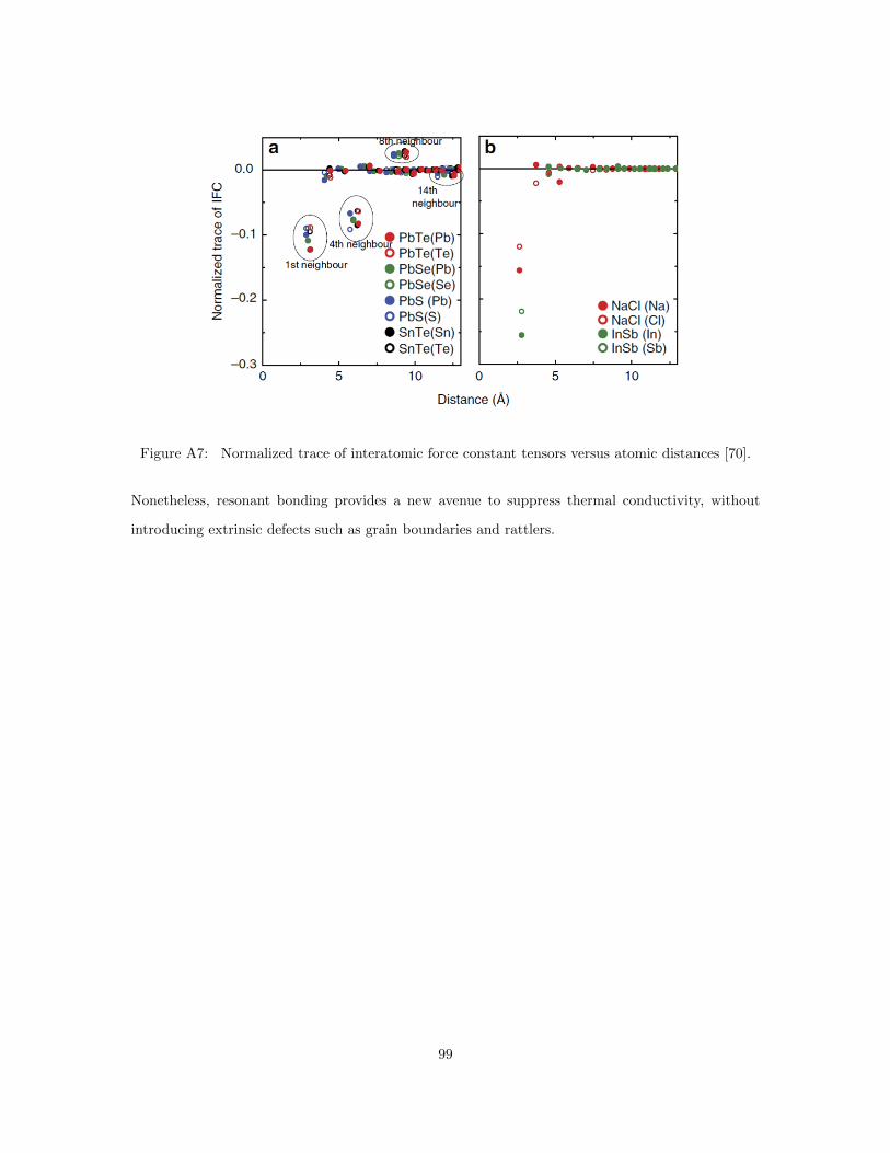
Figure A7: Normalized trace of interatomic force constant tensors versus atomic distances [70].
Nonetheless, resonant bonding provides a new avenue to suppress thermal conductivity, without
introducing extrinsic defects such as grain boundaries and rattlers.
99

Figure A8: Schematic diagram of experimental setup for TDTR [103].
Appendix D Time-Domain Thermoreflectance
Time-Domain Thermoreflectance (TDTR), is a method to measure the thermal properties
of the materials, such as thermal conductivity. TDTR can probe properties of thin film materials
which may be quite different from that of the bulk form. Basically, the reflectance of a material
changes with temperature, which provides information of its thermal properties. By measuring the
signal versus time delay, the data can be fitted to a model. For instance, for a semi-infinite solid,
the frequency domain is given by g (r) = e−qr
2πΛr , where q2 = iωd . Here Λ and r refer to the thermal
conductivity and the radial coordinate. With Hankel transform, one can have
G (k) =1
Λ(4π2k2 + q2)1/2
. (16)
Similar equation can be derived for the temperature on the surface of a layered structure. The setup
of TDTR is illustrated in Figure A8.
To investigate the surface thermal properties of SnSe, TDTR measurements were conducted
in Xiaojia Wang’s group in University of Minnesota. Figure A9 shows the image of the sample
surfaces, which were coated with aluminum with 80 nm thick before the measurements.
The results are shown in Figure A9. The fitted thermal conductivity of SnSe is 0.69− 0.7±
0.07 W/m ·K, lower than that of the bulk sample (∼ 1 W/m ·K at room temperature). Despite
100

Figure A9: TDTR results for SnSe single crystal.
the discrepancy between the values on the surface and in the bulk, it confirms that SnSe possesses
an low thermal conductivity.
101
Bibliography
[1] G.S. Nolas, J. Sharp, and J. Goldsmid. Thermoelectrics-Basic Principles and New MaterialsDevelopments. Springer, 2001.
[2] J. He and T.M. Tritt. Advances in thermoelectric materials research: Looking back and movingforward. Science, 357:1369, 2017.
[3] T.M. Tritt and M.A. Subramanian. Thermoelectric materials, phenomena, and applications:A birds eye view. MRS Bulletin, 31:188–198, 2017.
[4] G.J. Snyder and E.S. Toberer. Complex thermoelectric materials. Nature Materials, 7:105–114,2008.
[5] S.W. Angrisit. Direct Energy Conversion. Allyn and Bacon, 1982.
[6] G.D. Mahan. Figure of merit for thermoelectrics. Journal of Applied Physics, 65:1578–1583,1989.
[7] H.J. Goldsmid. Electronic Refrigeration. Pion Limited, 1986.
[8] J. He, Y. Liu, and R. Funahashi. Oxide thermoelectrics: The challenges, progress, and outlook.Journal of Materials Research, 26:1762–1772, 2011.
[9] A.M. Dehkordi, S. Bhattacharya, T. Darroudi, H.N. Alshareef, and T.M. Tritt. New insightson the synthesis and electronic transport in bulk polycrystalline Pr-doped SrTiO3-δ. Journalof Applied Physics, 117:055102, 2015.
[10] L.D. Zhao, C. Chang, G. Tan, and M.G. Kanatzidis. SnSe: a remarkable new thermoelectricmaterial. Energy & Environmental Science, 9:3044–3060, 2016.
[11] T.J. Seebeck. Ueber den Magnetismus der galvenischen Kette. Technical report for the RoyalPrussian Academy of Science, 1821.
[12] J.C.A. Peltier. Nouvelles experiences sur la caloricite des courants electrique. Annales deChimie et de Physique, 56:371–386, 1834.
[13] W. Thomson. On the mechanical theory of thermo-electric currents. Transactions of RoyalSociety of Edinburgh: Earth Sciences, 3:91–98, 1851.
[14] C. Goupil, W. Seifert, K. Zabrocki, E. Muller, and G.J. Snyder. Thermodynamics of thermo-electric phenomena and applications. Entropy, 13:1481–1517, 2011.
[15] A. Shakouri. Recent developments in semiconductor thermoelectric physics and materials.Annual Review of Materials Research, 41:399–431, 2011.
[16] L. Onsager. Reciprocal relations in irreversible processes. i. Physical Review, 37:405–426, 1931.
102

[17] G.A. Slack. New materials and performance limits for thermoelectric cooling. In D.M. Rowe,editor, CRC Handbook of Thermoelectrics. CRC Press, 1995.
[18] H.B. Callen. The application of Onsager’s reciprocal relations to thermoelectric, thermomag-netic, and galvanomagnetic effects. Physical Review, 73:1349–1358, 1948.
[19] R. Landauer. Spatial variation of currents and fields due to localized scatterers in metallicconduction. IBM Journal of Research and Development, 32:223–231, 1957.
[20] P.M. Chaikin. An introduction to thermopower for those who might want to use it to studyorganic conductors and superconductors. In V.Z. Kresin and W.A. Little, editors, OrganicSuperconductivity. Plenum Press, 1990.
[21] H.J. Goldsmid and J.W. Sharp. Estimation of the thermal band gap of a semiconductor fromSeebeck measurements. Journal of Electronic Materials, 28:869–872, 1999.
[22] M. Jonson and G.D. Mahan. Mott’s formula for the thermopower and the Wiedemann-Franzlaw. Physical Review B, 21:4223, 1980.
[23] Z.M. Gibbs, H.S. Kim, H. Wang, and G.F. Snyder. Band gap estimation from temperaturedependent Seebeck measurement deviations from the 2eSmaxTmax relation. Applied PhysicsLetters, 106:022112, 2015.
[24] M. Cutler and N.F. Mott. Observation of Anderson localization in an electron gas. PhysicalReview, 181:1336, 1969.
[25] A.F. Ioffe. Physics of Semiconductors. Academic Press, 1960.
[26] G.D. Mahan, L. Lindsay, and D.A. Broido. The Seebeck coefficient and phonon drag in silicon.Journal of Applied Physics, 116:245102, 2015.
[27] H.J. Goldsmid. Introduction to thermoelectricity. In R. Hull, R.M. Osgood Jr., J. Parsi, andH. Warlimont, editors, Springer Series in Materials Science. Springer, 2009.
[28] Y. Pei, X. Shi, A. LaLonde, H. Wang, L.D. Chen, and G.J. Snyder. Convergence of electronicbands for high performance bulk thermoelectrics. Nature, 473:66–69, 2011.
[29] Y. Liu, M. Zhou, and J. He. Towards higher thermoelectric performance of Bi2Te3 via defectengineering. Scripta Materlia, 111:39–43, 2016.
[30] D.T. Morelli, V. Jovovic, and J.P. Heremans. Intrinsically minimal thermal conductivity incubic I-V-VI2 semiconductors. Physical Review Letters, 101:035901, 2008.
[31] J.L. Cohn, G.S. Nolas, V. Fessatidis, T.H. Metcalf, and G.A. Slack. Glasslike heat conductionin high-mobility crystalline semiconductors. Physical Review Letters, 82:779–782, 1999.
[32] L.D. Zhao, S.H. Lo, Y.S. Zhang, H. Sun, G.J. Tan, C. Uher, C. Wolverton, V.P. Dravid, andM.G. Kanatzidis. Ultralow thermal conductivity and high thermoelectric figure of merit inSnSe crystals. Nature, 508:373–377, 2014.
[33] P.C. Wei, S. Bhattacharya, J. He, S. Neeleshwar, R. Podila, Y.Y. Chen, and A.M. Rao. Theintrinsic thermal conductivity of SnSe. Nature, 539:E1, 2016.
[34] D. Ibrahim, J.B. Vaney, S. Sassi, C. Candolfi, V. Ohorodniichuk, P. Levinsky, C. Sempri-moschnig, and A. Dauscher. Reinvestigation of the thermal properties of single-crystallineSnSe. Applied Physics Letters, 110:032103, 2017.
103

[35] Q. Zhang, B. Liao, Y. Lan, K. Lukas, W. Liu, K. Esfarjani, C. Opeil, D. Broido, G. Chen,and Z. Ren. Studies on thermoelectric properties of n-type polycrystalline SnSe1-xSx by iodinedoping. Advanced Energy Materials, 5:1500360, 2015.
[36] G. Shi and E. Kioupakis. Quasiparticle band structures and thermoelectric transport propertiesof p-type SnSe. Journal of Applied Physics, 117:065103, 2015.
[37] K. Kutorasinski, B. Wiendlocha, S. Kaprzyk, and J. Tobola. Electronic structure and thermo-electric properties of n- and p- type SnSe from first-principles caluculations. Physical ReviewB, 91:205201, 2015.
[38] R. Guo, X. Wang, Y. Kuang, and B. Huang. First-principles study of anisotropic thermoelectrictransport properties of IV-VI semiconductor compounds SnSe and SnS. Physical Review B,92:115202, 2015.
[39] A. Agarwal, M.N. Vashi, D. Lakshminarayana, and N.M. Batra. Electrical resistivityanisotropy in layered p-SnSe single crystals. Journal of Materials Science: Materials in Elec-tronics, 11:67–71, 2000.
[40] D.P. Padiyan, A. Marikani, and K.R. Murali. Electrical and photoelectrical properties ofvacuum deposited SnSe thin films. Crystal Research and Technology, 35:949–957, 2011.
[41] Y. Xie, H.L. Su, B. Li, and Y.T. Qian. A direct solvothermal route to nanocrystalline selenidesat low temperature. Materials Research Bulletin, 35:459–5464, 2000.
[42] S. Chen, K.F. Cai, and W.Y. Zhao. The effect of Te doping on the electronic structure andthermoelectric properties of SnSe. Physica B, 407:4154–4159, 2012.
[43] Z. Nabi, A. Kellou, S. Mecabih, A. Khalfi, and N. Benosman. Opto-electronic properties ofrutile SnO2 and orthorhombic SnS and SnSe compounds. Materials Science and Engineering:B, 98:104–115, 2003.
[44] S. Sassi, C. Candolfi, J.-B. Vaney, V. Ohorodniichuk, P. Masschelein, A. Dauscher, andB. Lenoir. Assessment of the thermoelectric performance of polycrystalline p-type SnSe. Ap-plied Physics Letters, 104:212105, 2014.
[45] C.L. Chen, H. Wang, Y.Y. Chen, T. Day, and G.J. Snyder. Thermoelectric properties of p-typepolycrystalline SnSe doped with Ag. Journal of Materials Chemistry A, 2:11171–11176, 2014.
[46] D. Bansal, J. Hong, C.W. Li, A.F. May, W. Porter, M.Y. Hu, D.L. Abernathy, and O. Delaire.Phonon anharmonicity and negative thermal expansion in SnSe. Physical Review B, 94:054307,2016.
[47] Y. Li, B. He, J.P. Heremans, and J.-C. Zhao. High-temperature oxidation behavior of ther-moelectric SnSe. Journal of Alloys and Compounds, 669:224–231, 2016.
[48] A.L. Pope, R.T. Littleton IV, and Terry M. Tritt. Apparatus for the rapid measurement ofelectrical transport properties for both needle-like and bulk materials. Review of ScientificInstruments, 72:3129–3131, 2001.
[49] A.L. Pope, B. Zawilski, and T.M. Tritt. Description of removable sample mount apparatus forrapid thermal conductivity measurements. Cryogenics, 41:725–731, 2001.
[50] A.Rudajevova, M.Svantner, D.Vasylyev, O.Musil, and V.Lang. Influence of radiation losseson thermal conductivity determination at low temperatures. International Journal of Ther-mophysics, 27:1241–1249, 2006.
104
[51] N.W. Ashcroft and N.D. Mermin. Solid State Physics. Thomson Learning, 1976.
[52] C.M. Bhandari and D.M. Rowe. Thermal conduction in semiconductors. Wiley Eastern Lim-ited, 1988.
[53] G.A. Slack and S. Galginaitis. Thermal conductivity and phonon scattering by magneticimpurities in CdTe. Physical Review, 133:A253, 1964.
[54] H. Xie, H. Wang, Y. Pei, C. Fu, X. Liu, G.J. Snyder, X. Zhao, and T. Zhu. Beneficialcontribution of alloy disorder to electron and phonon transport in half-Heusler thermoelectricmaterials. Advanced Functional Materials, 23:5123–5130, 2013.
[55] J. Yang, G.P. Meisner, and L. Chen. Strain field fluctuation effects on lattice thermal conduc-tivity of ZrNiSn-based thermoelectric compounds. Applied Physics Letters, 85:1140, 2004.
[56] J.E. Parrott. Heat conduction mechanisms in semiconducting materials. Revue internationaledes hautes temperatures et des refractaires, 16:393, 1979.
[57] C.W. Li, J. Hong, A.F. May, D. Bansal, S. Chi, T. Hong, G. Ehlers, and O. Delaire. Orbitallydriven giant phonon anharmonicity in SnSe. Nature Physics, 11:1063, 2015.
[58] Z. Zafa, A. Zafa, Y. Tian, Z. Cao, B. Jin, and Z. Shi. An easy approach to reveal the metallicnature of graphene by Breit-Wigner-Fano lineshapes using Raman spectroscopy. Journal ofRaman Spectroscopy, 48:1318–1322, 2017.
[59] M. Sist, J. Zhang, and Iversen B. Brummerstedt. Crystal structure and phase transition ofthermoelectric SnSe. Acta Crystallographica Section B: Structural Science, Crystal Engineeringand Materials, B72:310–316, 2016.
[60] M. Zhou, X. Chen, M. Li, and A. Du. Widely tunable and anisotropic charge carrier mobilityin monolayer tin(II) selenide using biaxial strain: a first-principles study. Journal of MaterialsChemistry C, 5:1247–1254, 2017.
[61] P.B. Allen. Improved callaway model for lattice thermal conductivity. Physical Review B,88:144302, 2013.
[62] J. Al-Otaibi and G.P. Srivastava. Three-phonon scattering processes and thermal conductivityin iv-chalcogenides. Journal of Physics: Condensed Matter, 27:335801, 2015.
[63] S. Baroni, S. de Gironcoli, A. Dal Corso, and P. Giannozzi. Phonons and related crystalproperties from density-functional perturbation theory. Reviews of Modern Physics, 73:515–562, 2001.
[64] P. Giannozzi, S. Baroni, N. Bonini, M. Calandra, R. Car, C. Cavazzoni, D. Ceresoli, G.L.Chiarotti, M. Cococcioni, I. Dabo, A. Dal Corso, S. de Gironcoli, S. Fabris, G. Fratesi,R. Gebauer, U. Gerstmann, C. Gougoussis, A. Kokalj, M. Lazzeri, L. Martin-Samos,N. Marzari, F. Mauri, R. Mazzarello, S.Paolini, A. Pasquarello, L. Paulatto, C. Sbraccia,S. Scandolo, G. Sclauzero, A.P. Seitsonen, A. Smogunov, P. Umari, and R.M Wentzcovitch.QUANTUM ESPRESSO: a modular and open-source software project for quantum simula-tions of materials. Journal of Physics: Condensed Matter, 21:395502, 2009.
[65] J.P. Perdew, K. Burke, and M. Ernzerhof. Generalized gradient approximation made simple.Physical Review Letters, 77:3865–3868, 1996.
[66] K.F. Garrity, J.W. Bennett, K.M. Rabe, and D. Vanderbilt. Pseudopotentials for high-throughput DFT. Computational Materials Science, 81:446, 2014.
105
[67] K. Lejaeghere, G. Bihlmayer, T. Bjorkman, P. Blaha, S. Blugel, V. Blum, D. Caliste, Ivano E.Castelli, S.J. Clark, A. Dal Corso, S. de Gironcoli, T. Deutsch, J.K. Dewhurst, I. Di Marco,C. Draxl, M. Du lak, O. Eriksson, J.A. Flores-Livas, K.F. Garrity, L. Genovese, P. Gi-annozzi, M. Giantomassi, S. Goedecker, X. Gonze, O. Granas, E.K.U. Gross, A. Gulans,F. Gygi, D.R. Hamann, P.J. Hasnip, N.A.W. Holzwarth, D. Iusan, D.B. Jochym, F. Jollet,D. Jones, G. Kresse, K. Koepernik, E. Kucukbenli, Y.O. Kvashnin, I.L.M. Locht, S. Lubeck,M. Marsman, N. Marzari, U. Nitzsche, L. Nordstrom, T. Ozaki, L. Paulatto, C.J. Pickard,W. Poelmans, M.I.J. Probert, K. Refson, M. Richter, G.-M. Rignanese, S. Saha, M. Scheffler,M. Schlipf, K. Schwarz, S. Sharma, F. Tavazza, P. Thunstrom, A. Tkatchenko, M. Torrent,D. Vanderbilt, M.J. van Setten, V. Van Speybroeck, J.M. Wills, J.R. Yates, G.-X. Zhang,and S. Cottenier. Reproducibility in density functional theory calculations of solids. Science,351:145–152, 2016.
[68] L. Liang, R. Rinaldi, and H. Schober. Neutron Applications in Earth, Energy and Environ-mental Sciences. Springer, 2009.
[69] E.S. Toberer, A. Zevalkink, and G.J. Snyder. Phonon engineering through crystal chemistry.Journal of Materials Chemistry, 21:15843, 2011.
[70] S. Lee, K. Esfarjani, T. Luo, J. Zhou, Z. Tian, and G. Chen. Resonant bonding leads to lowlattice thermal conductivity. Nature Communication, 5:3525, 2014.
[71] O. Madelung, U. Rossler, and M. Schulz, editors. Tin selenide (SnSe) optical properties,dielectric constants, pages 1–6. Springer Berlin Heidelberg, Berlin, Heidelberg, 1998.
[72] S. Baroni, P. Giannozzi, and A. Testa. Greens-function approach to linear response in solids.Physical Review Letters, 58:1861, 1987.
[73] X. Gonze. Adiabatic density-functional perturbation theory. Physical Review A, 52:1096–1114,1996.
[74] C.Chen, P.Jost, H.Volker, M.Kaminski, M.Wirtssohn, U.Engelmann, K.Kruger, F.Schlich,C.Schlockermann, R.P.S.M.Lobo, and M.Wuttig. Dielectric properties of amorphous phase-change materials. Physical Review B, 95:094111, 2017.
[75] O. Madelung, U. Rossler, and M. Schulz, editors. Lead telluride (PbTe) optical properties,dielectric constants, pages 1–10. Springer Berlin Heidelberg, Berlin, Heidelberg, 1998.
[76] A.R. Mackintosh. The Fermi surface of metals. Scientific American, 209:110–120, 1963.
[77] E.A. Albanesi, C.M.I. Okoye, C.O. Rodriguez, E.L. Peltzer y Blanca, and A.G. Petukhov.Electronic structure, structural properties, and dielectric functions of IV-VI semiconductors:PbSe and PbTe. Physical Review B, 61:16589–16595, 2000.
[78] K. Kuroki and R. Arita. Pudding mold band drives large thermopower in NaxCoO2. Journalof the Physical Society of Japan, 76:083707, 2007.
[79] C. Kittel. Introduction to Solid State Physics. John Wiley and Sons, 2004.
[80] M.I. Darby. Tables of the brillouin function and of the related function for the spontaneousmagnetization. British Journal of Applied Physics, 18:1415–1417, 1967.
[81] K.Peng, X.Lu, H.Zhan, S.Hui, X.Tang, G.Wang, J.Dai, C.Uher, G.Wang, and X.Zhou. Broadtemperature plateau for high ZTs in heavily doped p-type SnSe single crystals. Energy &Environmental Science, 9:454–460, 2016.
106

[82] M. Jin, H. Shao, H.Hu, D.Li, H.She, J.Xu, and J.Jiang. Growth and characterization of largesize undoped p-type SnSe single crystal by Horizontal Bridgman method. Journal of Alloysand Compounds, 712:857–862, 2017.
[83] M.Gharsallah, N.M. Nemes F. Serrano-Sanchez, F.J. Mompean, J.L. Martınez, M.T.Fernandez-Dıaz, F. Elhalouani, and J.A.Alonso. Giant Seebeck effect in Ge-doped SnSe. Sci-entific Reports, 6:26774, 2016.
[84] J.G. Yu, A.S. Yue, and O.M. Stafsudd Jr. Growth and electronic properties of the SnSesemiconductor. Journal of Crystal Growth, 54:248–252, 1981.
[85] G.Duvjir, T.Min, T.T. Ly, T.Kim, A.-T.Duong, S.Cho, S.H.Rhim, J.Lee, and J.Kim. Originof p-type characteristics in a SnSe single crystal. Applied Physics Letters, 110:262106, 2017.
[86] B.D. Cullity and S.R. Stock. Elements of X-Ray Diffraction, 3rd Ed. Prentice-Hall Inc., 2001.
[87] M. Achimovicova, K. Lucenildo da Silva, N. Daneu, A. Recnik, S. Indris, H. Hain, M. Scheuer-mann, H. Hahnd, and V. Sepelak. Structural and morphological study of mechanochemicallysynthesized tin diselenide. Journal of Materials Chemistry, 21:5873–5876, 2011.
[88] N.F. Mott. Conduction in non-crystalline materials. Philosophical Magazine, 19:835–852, 1969.
[89] P.W. Anderson. Absence of diffusion in certain random lattices. Physical Review, 109:1492,1958.
[90] P.P.Edwards and M.J.Sienko. Universality aspects of the metal-nonmetal transition in con-densed media. Physical Review B, 16:2575–2581, 1978.
[91] T. Siegrist, P.Jost, H.Volker, M.Woda, P.Merkelbach, C.Schlockermann, and M.Wuttig.Disorder-induced localization in crystalline phase-change materials. Nature Materials, 10:202–208, 2011.
[92] E.Abrahams, S.V.Kravchenko, and M.P.Sarachik. Colloquium: Metallic behaviour and relatedphenomena in two dimensions. Reviews of Modern Physics, 73:251–266, 2001.
[93] Q.Lu, M.Wu, D.Wu, C.Change, Y-.P.Guo, W.Li C-.S.Zhou, X-.M.Ma, G.Wang, L-.D.Zhao,L.Huang, C.Liu, and J.He. Unexpected large hole effective masses in SnSe revealed by angle-resolved photoemission sepectroscopy. Physical Review Letters, 119:116401, 2017.
[94] J.M. Skelton, L.A. Burton, S.C. Parker, A. Walsh, C.-E. Kim, A. Soon, J. Buckridge, A.A.Sokol, C.R.A. Catlow, A. Togo, and I. Tanaka. Anharmoncity in the high-temperaure Cmcmphase of SnSe: Soft modes and three-phonon interactions. Physical Review Letters, 117:075502,2016.
[95] R.H. Mitchell, M.D. Welch, and A.R. Chakhmouradian. Nomenclature of the perovskite su-pergroup: A hierarchical system of classification based on crystal structure and composition.Mineralogical Magazine, 81:411–461, 2017.
[96] Y. Rocard. Thermodynamique, 2nd ed. Masson, 1967.
[97] H.B. Callen. Thermodynamics. John Wiley & Sons, 1960.
[98] M. Wuttig and N. Yamada. Phase-change materials for rewriteable data storage. NatureMaterials, 6:824–832, 2007.
[99] K. Shportko, S. Kremers, M. Woda, D. Lencer, J. Robertson, and M. Wuttig. Resonantbonding in crystalline phase-change materials. Nature Materials, 7:653–658, 2008.
107

[100] P.B. Littlewood. Dielectric-constant of cubic IVVI compounds. Journal of Physics C: SolidState Physics, 12:4459–4468, 1979.
[101] P.B. Littlewood. The crystal structure of IVVI compounds: I. classification and description.Journal of Physics C: Solid State Physics, 13:4855–4873, 1980.
[102] D. Lencer, M. Salinga, B. Grabowski, T. Hickel, J. Neugebauer, and M. Wuttig. A map forphase-change materials. Nature Materials, 7:972–977, 2008.
[103] C.Wei, X.Zheng, D.G. Cahill, and J.-C.Zhao. Invited article: Micron resolution spatiallyresolved measurement of heat capacity using dual-frequency time-domain thermoreflectance.The Review of Scientific Instruments, 84:071301, 2013.
108