on optimization of manufacturing of multichannel heterotransistors to increase their integration...
TRANSCRIPT

7/23/2019 On Optimization of Manufacturing of Multichannel Heterotransistors to Increase Their Integration Rate
http://slidepdf.com/reader/full/on-optimization-of-manufacturing-of-multichannel-heterotransistors-to-increase 1/14
International Journal of Recent advances in Physics (IJRAP) Vol.4, No.4, November 2015
DOI : 10.14810/ijrap.2015.4401 1
ON OPTIMIZATION OF MANUFACTURING OF MULTI-
CHANNEL HETEROTRANSISTORS TO INCREASE
THEIR INTEGRATION RATE
E.L. Pankratov1, E.A. Bulaeva
1,2
1 Nizhny Novgorod State University, 23 Gagarin avenue , Nizhny Novgorod, 603950,
Russia2
Nizhny Novgorod State University of Architecture and Civil Engineering , 65 Il'insky
street , Nizhny Novgorod , 603950, Russia
A BSTRACT
In this paper we consider an approach to increase integration rate of field-effect heterotransistors. Frame-
work the approach we consider a heterostructure with specific configuration. After manufacturing theheterostructure we consider doping of required areas of the heterostructure by diffusion or ion implanta-
tion. The doping finished by optimized annealing of dopant and/or radiation defects. Framework this paper
we consider a possibility to manufacture with several channels. Manufacturing multi-channel transistors
gives us a possibility the to increase integration rate of transistors and to increase electrical current
through the transistor.
K EYWORDS
Field-effect heterotransistors; multi-channel heterotransistors; increasing of integration rate
1. INTRODUCTION
In the present time integration rate of elements of integrated circuits intensively increasing [1-6].Increasing of the integration rate leads to necessity to decrease dimensions of these elements. Are
they widely using to decrease these elements laser and microwave types of annealing [7-11]. It
could be also used radiation processing of doped materials to solve the same problem [12,13].
Fig. 1a. Heterostructure which includes into itself a substrate and an epitaxial layer. Side view

7/23/2019 On Optimization of Manufacturing of Multichannel Heterotransistors to Increase Their Integration Rate
http://slidepdf.com/reader/full/on-optimization-of-manufacturing-of-multichannel-heterotransistors-to-increase 2/14
International Journal of Recent advances in Physics (IJRAP) Vol.4, No.4, November 2015
2
In this paper we consider manufacturing a multi-channel heterotransistor with common gate. The
heterotransistor has been manufactured framework a heterostructure, which include into itself asubstrate and an epitaxial layer. The epitaxial layer includes into itself several sections (see Fig.
1). After manufacturing of the required quantity of channels they should be doped to generation
required type of conductivity (n or p). Farther we consider annealing of dopant and/or radiationdefects. Increasing of annealing time leads to increasing of quantity of dopant in nearest materi-
als. Decreasing of annealing time give not possibility to organize full doping of channels of tran-sistors. Main aim of the present paper is analysis of spatio-temporal distributions of concentra-
tions of dopant and radiation defects and temperature to determine conditions to decrease dimen-
sion of the considered heterotransistor.
Fig. 1b. Heterostructure which includes into itself a substrate and an epitaxial layer. Top view
2. METHOD OF SOLUTION
We solved our aim by calculation of spatio-temporal distributions of concentrations of dopant and
radiation defects. We determine the required distribution of concentrations of dopant by solutionof the following boundary problem
( ) ( ) ( ) ( )
+
+
=
z
t z y xC D
z y
t z y xC D
y x
t z y xC D
xt
t z y xC C C C
∂
∂
∂
∂
∂
∂
∂
∂
∂
∂
∂
∂
∂
∂ ,,,,,,,,,,,,. (1)
( )0
,,,
0
=∂
∂
= x x
t z y xC ,
( )0
,,,=
∂
∂
= x L x x
t z y xC ,
( )0
,,,
0
=∂
∂
= y y
t z y xC ,
( )0
,,,=
∂
∂
= y L x y
t z y xC ,
( )0
,,,
0
=∂
∂
= z z
t z y xC ,
( )0
,,,=
∂
∂
= z L x z
t z y xC , C ( x, y, z,0)=f ( x, y, z). (2)
Function C ( x, y, z,t ) describes the spatio-temporal distribution of concentration of dopant; T is the
temperature of annealing; DС is the dopant diffusion coefficient. Dopant diffusion coefficient willhave different values in different materials. The value will be changed during heating and cooling
of heterostructure (with account Arrhenius law). Approximation of dopant diffusion coefficientby the following function [13-15]
( ) ( )
( )( ) ( )
( )
++
+=
2*
2
2*1
,,,,,,1
,,,
,,,1,,,
V
t z y xV
V
t z y xV
T z y xP
t z y xC T z y x D D
LC ς ς ξ
γ
γ
. (3)
7/23/2019 On Optimization of Manufacturing of Multichannel Heterotransistors to Increase Their Integration Rate
http://slidepdf.com/reader/full/on-optimization-of-manufacturing-of-multichannel-heterotransistors-to-increase 3/14
International Journal of Recent advances in Physics (IJRAP) Vol.4, No.4, November 2015
3
Function D L( x, y, z,T ) describes the spatial and temperature dependences of dopant diffusion coef-
ficient. One can find these dependences due to presents several layers in heterostructure and theArrhenius law, respectively. Function P ( x, y, z,T ) describes the limit of solubility of dopant. Pa-
rameter γ ∈[1,3] has different values in different materials [14]. The function V ( x, y, z,t ) describesthe spatio-temporal distribution of concentration of radiation vacancies. V
* is the equilibrium dis-
tribution of concentration of vacancies. Dependence of dopant diffusion coefficient on concentra-tion of dopant has been described in details in [14]. It is known, that doping of materials by diffu-
sion did not leads to generation radiation defects. In this situation ζ 1= ζ 2= 0. It should be also not-
ed, that we solved more common boundary problem in comparison with recently published works[1-15].
We determine spatio-temporal distributions of concentrations of radiation defects by solving thefollowing boundary problem [13,15]
( )( )
( )( )
( )( ) ×−
∂
∂
∂
∂+
∂
∂
∂
∂=
∂
∂T z y xk
y
t z y x I T z y x D
y x
t z y x I T z y x D
xt
t z y x I I I I I
,,,,,,
,,,,,,
,,,,,,
,
( ) ( ) ( )
( ) ( ) ( )t z y xV t z y x I T z y xk z
t z y x I T z y x D zt z y x I V I I ,,,,,,,,,
,,,,,,,,, ,
2
−
∂
∂
∂
∂
+× (4)
( )( )
( )( )
( )( ) ×−
∂
∂
∂
∂+
∂
∂
∂
∂=
∂
∂T z y xk
y
t z y xV T z y x D
y x
t z y xV T z y x D
xt
t z y xV V V V V
,,,,,,
,,,,,,
,,,,,,
,
( ) ( ) ( )
( ) ( ) ( )t z y xV t z y x I T z y xk z
t z y xV T z y x D
zt z y xV
V I V ,,,,,,,,,
,,,,,,,,,
,
2−
∂
∂
∂
∂+× .
Boundary and initial conditions for these equations are
( )0
,,,
0
=∂
∂
= x x
t z y x ρ ,
( )0
,,,=
∂
∂
= x L x x
t z y x ρ ,
( )0
,,,
0
=∂
∂
= y y
t z y x ρ ,
( )0
,,,=
∂
∂
= y L y y
t z y x ρ ,
( )0
,,,
0
=∂
∂
= z z
t z y x ρ ,
( )0
,,,=
∂
∂
= z L z z
t z y x ρ , ρ ( x, y, z,0)=f ρ ( x, y, z). (5)
Here ρ = I ,V . The function I ( x, y, z,t ) describes the spatio-temporal distribution of concentration of
radiation interstitials. The functions D ρ ( x, y, z,T ) describes the approximations of diffusion coeffi-
cients of point radiation defects. Terms V 2( x, y, z,t ) and I
2( x, y, z,t ) correspond to generation
divacancies and diinterstitials. The function k I ,V ( x, y, z,T ) describes the parameter of recombination
of point radiation defects. The functions k I , I ( x, y, z,T ) and k V ,V ( x, y, z,T ) describe the parameters of
generation of simplest complexes of point radiation defects.
Now we calculate distributions of concentrations of divacancies Φ V ( x, y, z,t ) and diinterstitials
Φ I ( x, y, z,t ) in space and time by solving the following boundary problem [13,15]
( )( )
( )( )
( )+
Φ+
Φ=
ΦΦΦ
y
t z y xT z y x D
y x
t z y xT z y x D
xt
t z y x I
I
I
I
I
∂
∂
∂
∂
∂
∂
∂
∂
∂
∂ ,,,,,,
,,,,,,
,,,
( ) ( )
( ) ( ) ( ) ( )t z y x I T z y xk t z y x I T z y xk z
t z y xT z y x D
z I I I
I
I ,,,,,,,,,,,,
,,,,,,
2
, −+
Φ+
Φ
∂
∂
∂
∂ (6)
7/23/2019 On Optimization of Manufacturing of Multichannel Heterotransistors to Increase Their Integration Rate
http://slidepdf.com/reader/full/on-optimization-of-manufacturing-of-multichannel-heterotransistors-to-increase 4/14
International Journal of Recent advances in Physics (IJRAP) Vol.4, No.4, November 2015
4
( )( )
( )( )
( )+
Φ+
Φ=
ΦΦΦ
y
t z y xT z y x D
y x
t z y xT z y x D
xt
t z y xV
V
V
V
V
∂
∂
∂
∂
∂
∂
∂
∂
∂
∂ ,,,,,,
,,,,,,
,,,
( ) ( )
( ) ( ) ( ) ( )t z y xV T z y xk t z y xV T z y xk z
t z y xT z y x D
zV V V
V
V ,,,,,,,,,,,,
,,,,,, 2
, −+
Φ+
Φ∂
∂
∂
∂ ,
( )0
,,,
0
=∂
Φ∂
= x x
t z y x ρ ,
( )0
,,,=
∂
Φ∂
= x L x x
t z y x ρ ,
( )0
,,,
0
=∂
Φ∂
= y y
t z y x ρ ,
( )0
,,,=
∂
Φ∂
= y L y y
t z y x ρ ,
( )0
,,,
0
=∂
Φ∂
= z z
t z y x ρ ,
( )0
,,,=
∂
Φ∂
= z L z z
t z y x ρ , Φ I ( x, y, z,0)=f Φ I ( x, y, z), Φ V ( x, y, z,0)=f Φ V ( x, y, z). (7)
The functions DΦρ ( x, y, z,T ) describe the diffusion coefficients of the above complexes of radiation
defects. The functions k I ( x, y, z,T ) and k V ( x, y, z,T ) describe the parameters of decay of these com-
plexes. In this situation boundary problems Eqs.(4)-(7) are generalization of analogous problemsin [13-15].
We determine distribution of temperature in space and time as solution of the second law of Fou-rier [14]
( ) ( )
( ) ( )
( ) ( )
+
∂
∂
∂
∂+
∂
∂
∂
∂=
∂
∂
y
t z y xT T z y x
y x
t z y xT T z y x
xt
t z y xT T c
,,,,,,
,,,,,,
,,,λ λ
( ) ( )
( )t z y x p z
t z y xT T z y x
z,,,
,,,,,, +
∂
∂
∂
∂+ λ . (8)
Boundary and initial conditions for the Eq. (8) are
( )0
,,,
0
=∂
∂
= x x
t z y xT ,
( )0
,,,=
∂
∂
= x L x x
t z y xT ,
( )0
,,,
0
=∂
∂
= y y
t z y xT ,
( )0
,,,=
∂
∂
= y L x y
t z y xT ,
( ) 0,,,
0
=∂
∂
= z z
t z y xT , ( ) 0,,, =∂
∂
= z L x z
t z y xT , T ( x, y, z,0)=f T ( x, y, z), (9)
Function T ( x, y, z,t ) describes distribution of temperature in space and time during annealing of
dopant and/or radiation defects. Function c (T )= cass[1-η exp(-T ( x, y, z,t )/ T d )] describes dependenceof the heat capacitance on temperature. In the considered situation current temperature is approx-
imately equal or larger, than Debye temperature T d . In this situation we have a possibility to con-
sider the following limiting case c (T )≈cass) [14]. The function λ describes the heat conductioncoefficient. The heat conduction coefficient depends on properties of materials and temperature
and could be approximated by the following function λ ( x, y, z,T )=λ ass( x, y, z)[1+ µ (T d / T ( x, y, z,t ))ϕ ]
[14]). The function describes p( x, y, z,t ) is the volumetric density of power of heating; α ( x, y, z,T )=λ ( x, y, z,T )/ c(T ) is the thermal diffusivity.
We calculate distribution of concentrations of dopant and radiation defects and temperature inspace and time by method of averaging of function corrections [16-18] with decreasing quantity
of iteration steps [17]. To use the approach we consider solutions of Eqs. (1), (4), (6), (8) with
averaged values of diffusion coefficients D0 L, D0 I , D0V , D0Φ I , D0Φ V , zero values of parameters ofrecombination of radiation defects and parameters of generation and decay of their complexes as
initial-order approximations of required concentrations. The initial-order approximations could bewritten as
7/23/2019 On Optimization of Manufacturing of Multichannel Heterotransistors to Increase Their Integration Rate
http://slidepdf.com/reader/full/on-optimization-of-manufacturing-of-multichannel-heterotransistors-to-increase 5/14
International Journal of Recent advances in Physics (IJRAP) Vol.4, No.4, November 2015
5
( ) ( ) ( ) ( ) ( )∑+=∞
=11
21,,,
nnC nnnnC
z y x z y x
t e zc yc xcF L L L L L L
t z y xC ,
( ) ( ) ( ) ( ) ( )∑+=∞
=11
21,,,
nnI nnnnI
z y x z y x
t e zc yc xcF L L L L L L
t z y x I ,
( ) ( ) ( ) ( ) ( )∑+=∞
=11
21,,,
nnV nnnnV
z y x z y x
t e zc yc xcF L L L L L L
t z y xV ,
( ) ( ) ( ) ( ) ( )∑+=Φ∞
=ΦΦ
11
21,,,
nnnnnn
z y x z y x
I t e zc yc xcF
L L L L L Lt z y x
I I ,
( ) ( ) ( ) ( ) ( )∑+=Φ∞
=ΦΦ
11
21,,,
nnnnnn
z y x z y x
V t e zc yc xcF L L L L L L
t z y xV V
,
( ) ( ) ( ) ( ) ( )∑+=∞
=11
21,,,
nnT nnnnT
z y x z y x
t e zc yc xcF L L L L L L
t z y xT ,
where ( )
++−=
2220
22 111exp
z y x
n L L L
t Dnt e ρ ρ π , ( ) ( ) ( ) ( )∫ ∫ ∫=
x y z L L L
nnnnud vd wd wvu f wcvcucF
0 0 0
,, ρ ρ ,
( )
++−=
2220
22 111exp
z y x
nT L L L
t nt e α π , cn( χ ) = cos(π n χ / L χ ).
One could calculate approximations of the second- and other orders framework classical iterationprocedure of method of averaging of function corrections [16-18]. Framework this procedure to
determine the n-th-order approximation of concentrations of dopant and radiation defects we shall
replace the required functions C ( x, y, z,t ), I ( x, y, z,t ), V ( x, y, z,t ), Φ I ( x, y, z,t ), Φ V ( x, y, z,t ) and T ( x, y, z,t )in the right sides of Eqs. (1), (4), (6), (8) on the following sums α n ρ + ρ n-1( x, y, z,t ), when α n ρ are notyet known average values of the n-th-order approximation of the above concentrations. The re-
placement leads to the following relations for the second-order approximations of the required
concentrations
( )( )
( ) ( )
( )( )
×
++=
∗∗ x
t z y xC
V
t z y xV
V
t z y xV T z y x D
xt
t z y xC L
∂
∂ ς ς
∂
∂
∂
∂ ,,,,,,,,,1,,,
,,,1
2
2
21
2
( )[ ]( )
( ) ( ) ( )
( )
×
+++
++×
∗∗ 2
2
21
12 ,,,,,,1,,,
,,,
,,,1
V
t z y xV
V
t z y xV T z y x D
yT z y xP
t z y xC L
C ς ς ∂
∂ α ξ
γ
γ
( )[ ]( )
( ) ( )[ ]( )
×
+++
++×
T z y xP
t z y xC
z y
t z y xC
T z y xP
t z y xC C C
,,,
,,,1
,,,
,,,
,,,1 12112
γ
γ
γ
γ α
ξ ∂
∂
∂
∂ α ξ
( ) ( ) ( )
( )( )
++×
∗∗ z
t z y xC
V
t z y xV
V
t z y xV T z y x D
L∂
∂ ς ς
,,,,,,,,,1,,, 1
2
2
21 (10)

7/23/2019 On Optimization of Manufacturing of Multichannel Heterotransistors to Increase Their Integration Rate
http://slidepdf.com/reader/full/on-optimization-of-manufacturing-of-multichannel-heterotransistors-to-increase 6/14
International Journal of Recent advances in Physics (IJRAP) Vol.4, No.4, November 2015
6
( )( )
( )( )
( )+
+
=
y
t z y x I T z y x D
y x
t z y x I T z y x D
xt
t z y x I I I
∂
∂
∂
∂
∂
∂
∂
∂
∂
∂ ,,,,,,
,,,,,,
,,,112
( ) ( )
( ) ( )[ ] ( )[ ]−++−
+ t z y xV t z y x I T z y xk
z
t z y x I T z y x D
zV I V I I
,,,,,,,,,,,,
,,,1212,
1 α α ∂
∂
∂
∂
( ) ( )[ ]2
12,,,,,,, t z y x I T z y xk
I I I +− α (11)
( )( )
( )( )
( )+
+
=
y
t z y xV T z y x D
y x
t z y xV T z y x D
xt
t z y xV V V
∂
∂
∂
∂
∂
∂
∂
∂
∂
∂ ,,,,,,
,,,,,,
,,, 112
( ) ( )
( ) ( )[ ] ( )[ ]−++−
+ t z y xV t z y x I T z y xk
z
t z y xV T z y x D
zV I V I V
,,,,,,,,,,,,
,,,1212,
1 α α ∂
∂
∂
∂
( ) ( )[ ]2
12,,,,,,, t z y xV T z y xk
V V V +− α
( )( )
( )( ) ( )++
Φ=
ΦΦ
t z y x I T z y xk x
t z y xT z y x D
xt
t z y x I I
I
I
I ,,,,,,,,,
,,,,,, 2
,
12
∂
∂
∂
∂
∂
∂
( ) ( )
( ) ( )
−
Φ+
Φ+
ΦΦ
z
t z y xT z y x D
z y
t z y xT z y x D
y
I
I
I
I ∂
∂
∂
∂
∂
∂
∂
∂ ,,,,,,
,,,,,, 11
( ) ( )t z y x I T z y xk I
,,,,,,− (12)
( )( )
( )( ) ( )++
Φ=
ΦΦ
t z y xV T z y xk x
t z y xT z y x D
xt
t z y xV V
V
V
V ,,,,,,,,,
,,,,,, 2
,
12
∂
∂
∂
∂
∂
∂
( ) ( ) ( ) ( )−
Φ+
Φ+
ΦΦ
z
t z y xT z y x D
z y
t z y xT z y x D
y
V
V
V
V ∂
∂
∂
∂
∂
∂
∂
∂ ,,,,,,
,,,,,, 11
( ) ( )t z y xV T z y xk V
,,,,,,− .
( )( )
( )( )[ ]
+
∂
+∂
+
∂
∂=
∂
∂
x
t z y xT
t z y xT
T z y x
xt
t z y xT c T d
ass
,,,
,,,1,,
,,, 122 α µ λ
ϕ
( )( )
( )[ ]+
∂
+∂
+
∂
∂+
y
t z y xT
t z y xT
T z y x
y
T d
ass
,,,
,,,1,, 12α
µ λ
ϕ
( )( )
( )[ ]( )t z y x p
z
t z y xT
t z y xT
T z y x
z
T d
ass,,,
,,,
,,,1,, 12
+
∂
+∂
+
∂
∂+
α µ λ
ϕ
. (13)
Integration of both sides of Eqs. (10)-(13) on time gives us possibility to obtain relations for the
second-order approximations of the required concentrations in the final form
7/23/2019 On Optimization of Manufacturing of Multichannel Heterotransistors to Increase Their Integration Rate
http://slidepdf.com/reader/full/on-optimization-of-manufacturing-of-multichannel-heterotransistors-to-increase 7/14
International Journal of Recent advances in Physics (IJRAP) Vol.4, No.4, November 2015
7
( ) ( ) ( ) ( )
( )( )
∫ ×
++=
∗∗
t
L x
z y xC
V
z y xV
V
z y xV T z y x D
xt z y xC
0
1
2
2
212
,,,,,,,,,1,,,,,,
∂
τ ∂ τ ς
τ ς
∂
∂
( )[ ]
( )
( ) ( )
( )
∫ ×
+++
++×
∗∗
t C
V
z y xV
V
z y xV
yd
T z y xP
z y xC
0 2
2
21
12,,,,,,
1,,,
,,,1
τ ς
τ ς
∂
∂ τ
τ α ξ
γ
γ
( ) ( )[ ]
( )( ) ( )
∫ ×+
++×
t C
L z
z y xC
zd
y
z y xC
T z y xP
z y xC T z y x D
0
1112,,,,,,
,,,
,,,1,,,
∂
τ ∂
∂
∂ τ
∂
τ ∂ τ α ξ
γ
γ
( ) ( ) ( )
( ) ( ) z y x f d
V
z y xV
V
z y xV T z y x D
C L,,
,,,,,,1,,,
2
2
21 +
++×
∗∗ τ
τ ς
τ ς (10 a)
( ) ( ) ( )
( ) ( )
+
∫+
∫=
t
I
t
I d y
z y x I T z y x D
yd
x
z y x I T z y x D
xt z y x I
0
1
0
1
2
,,,,,,
,,,,,,,,, τ
∂
τ ∂
∂
∂ τ
∂
τ ∂
∂
∂
( ) ( )
( ) ( )[ ] −∫ +−
∫+
t
I I I
t
I d z y x I T z y xk d z
z y x I T z y x D
z 0
2
12,0
1 ,,,,,,,,,
,,, τ τ α τ ∂
τ ∂
∂
∂
( ) ( )[ ] ( )[ ] ( ) z y x f d z y xV z y x I T z y xk I
t
V I V I ,,,,,,,,,,,
01212,
+∫ ++− τ τ α τ α (11 a)
( ) ( ) ( )
( ) ( )
+
∫+
∫=
t
V
t
V d
y
z y xV T z y x D
yd
x
z y xV T z y x D
xt z y xV
0
1
0
1
2
,,,,,,
,,,,,,,,, τ
∂
τ ∂
∂
∂ τ
∂
τ ∂
∂
∂
( ) ( )
( ) ( )[ ] −∫ +−
∫+
t
I V V
t
V d z y xV T z y xk d
z
z y xV T z y x D
z 0
2
12,
0
1 ,,,,,,,,,
,,, τ τ α τ
∂
τ ∂
∂
∂
( ) ( )[ ] ( )[ ] ( ) z y x f d z y xV z y x I T z y xk V
t
V I V I ,,,,,,,,,,,
01212,
+∫ ++− τ τ α τ α
( ) ( ) ( )
( ) ( ) +∫−
∫
Φ=Φ
Φ
t
I
t I
I I d z y x I T z y xk d
x
z y xT z y x D
xt z y x
00
1
2,,,,,,
,,,,,,,,, τ τ τ
∂
τ ∂
∂
∂
( ) ( )
( ) ( )
+
∫
Φ+
∫
Φ+
ΦΦ
t I
I
t I
I d
z
z y xT z y x D
zd
y
z y xT z y x D
y 0
1
0
1,,,
,,,,,,
,,, τ ∂
τ ∂
∂
∂ τ
∂
τ ∂
∂
∂
( ) ( ) ( ) z y x f d z y x I T z y xk I
t
I I ,,,,,,,,0
2
, Φ+∫+ τ τ (12 a)
( ) ( ) ( )
( ) ( ) +∫−
∫
Φ=Φ
Φ
t
V
t V
V V d z y xV T z y xk d
x
z y xT z y x D
xt z y x
00
1
2,,,,,,
,,,,,,,,, τ τ τ
∂
τ ∂
∂
∂

7/23/2019 On Optimization of Manufacturing of Multichannel Heterotransistors to Increase Their Integration Rate
http://slidepdf.com/reader/full/on-optimization-of-manufacturing-of-multichannel-heterotransistors-to-increase 8/14
International Journal of Recent advances in Physics (IJRAP) Vol.4, No.4, November 2015
8
( ) ( )
( ) ( )
+
∫
Φ+
∫
Φ+
ΦΦ
t V
V
t V
V d
z
z y xT z y x D
zd
y
z y xT z y x D
y 0
1
0
1,,,
,,,,,,
,,, τ ∂
τ ∂
∂
∂ τ
∂
τ ∂
∂
∂
( ) ( ) ( ) z y x f d z y xV T z y xk V
t
V V ,,,,,,,,
0
2
, Φ+∫+ τ τ ,
( ) ( )( )
( )[ ]+
∫
∂
+∂
+
∂
∂=
t T d
assd
x
z y xT
z y xT
T z y x
xt z y xcT
0
12 ,,,
,,,1,,,,, τ
τ α
τ µ λ
ϕ
( ) ( )( )
( )[ ]+
∫
∂
+∂
+
∂
∂++
t T d
assT d
y
z y xT
z y xT
T z y x
y z y x f
0
12 ,,,
,,,1,,,, τ
τ α
τ µ λ
ϕ
(13 a)
( )( )
( )[ ]( )∫+
∫
∂
+∂
+
∂
∂+
t t T d
assd z y x pd
z
z y xT
z y xT
T z y x
z 00
12 ,,,,,,
,,,1,, τ τ τ
τ α
τ µ λ
ϕ
.
One could calculate average values of the second-orders approximations of the required concen-trations and temperature by the standard relation [16-18]
( ) ( )[ ]∫ ∫ ∫ ∫ −Θ
=Θ
0 0 0 0122
,,,,,,1 x y z L L L
z y x
t d xd yd zd t z y xt z y x L L L
ρ ρ α ρ . (14)
Final relations for the required average values by substitution of the relations (10a)-(13a) into therelation (14)
( )∫ ∫ ∫= x y z L L L
C
z y x
С xd yd zd z y x f
L L L 0 0 02
,,1
α , (15)
( ) [{ −+−−+++= 112010200
2
0021001
00
241
2
1 IV II IV V II IV V II IV
II
I A A A A A A A
A
α α α
( )00
0021001
2
1
0 0 0 2
1,,
1
II
IV V II IV L L L
I
z y x A
A A A xd yd zd z y x f
L L L
x y z α +++−
∫ ∫ ∫− , (16)
( )
4
313
4
2
3
4
24
442
1
B
A B
A
B y B y B
A B
BV
+−
−+−
+=α .
Parameters Aabij and other parameters in the relations (16) are presented in the Appendix. Parame-
ters α abij and other parameters in the relations (16) could be written as
( ) ( ) ( ) +∫ ∫ ∫ ∫−ΘΘ
−=
Θ
Φ0 0 0 0
202 ,,,,,,1 x y z
I
L L L
I
z y x
II t d xd yd zd t z y x I T z y xk t L L L
Aα
( )∫ ∫ ∫+ Φ
x y z L L L
I
z y x
xd yd zd z y x f L L L 0 0 0
,,1
(17)
7/23/2019 On Optimization of Manufacturing of Multichannel Heterotransistors to Increase Their Integration Rate
http://slidepdf.com/reader/full/on-optimization-of-manufacturing-of-multichannel-heterotransistors-to-increase 9/14
International Journal of Recent advances in Physics (IJRAP) Vol.4, No.4, November 2015
9
( ) ( ) ( ) +∫ ∫ ∫ ∫−ΘΘ
−=Θ
Φ0 0 0 0
202,,,,,,
1 x y z
V
L L L
V
z y x
VV t d xd yd zd t z y xV T z y xk t
L L L Aα
( )∫ ∫ ∫+ Φ
x y z L L L
V
z y x
xd yd zd z y x f L L L 0 0 0
,,1
.
The above substitution leads to obtaining equation for parameter α 2C . Solution of the equation
will be different for different values of parameter γ . We used the second-order approximationsframework method of averaging of function corrections with decreased quantity of iterative steps
for analysis of spatio-temporal distributions of concentrations of dopant and radiation defects andtemperature. The second-order approximation is usually a sufficient approximation to obtain
qualitative and some quantitative results. We checked our analytical results by numerical ap-proaches.
3. Discussion
Based on recently calculated relations we analyzed redistribution of dopant and radiation defects.
Figures 2a and 2b show distributions of concentrations of infused (Fig. 2a) and implanted (Fig.2b) dopants in channels and in nearest areas. We calculate the above distribution for larger value
of dopant diffusion coefficient in doped materials in comparison with the analogous coefficient inundoped area. In this case it is possible to increase density of channels in transistors and, as aconsequence, to decrease dimensions of multi-channel transistor. At the same time the considered
approach of doping gives us possibility to increase homogeneity of concentrations of dopants in
channels of the considered transistors. In this situation one can obtain increasing density of elec-
trical current in the channels at fixed value of maximal heating of the doped material or to de-crease length of channels. It should be noted, that using ion implantation gives us possibility to
increase homogeneity of concentrations of dopants in channels and at the same time to decreasetheir quantities in nearest materials due to radiation-induced diffusion.
Analysis of changing of concentration of dopant in time shown necessity of optimization of an-
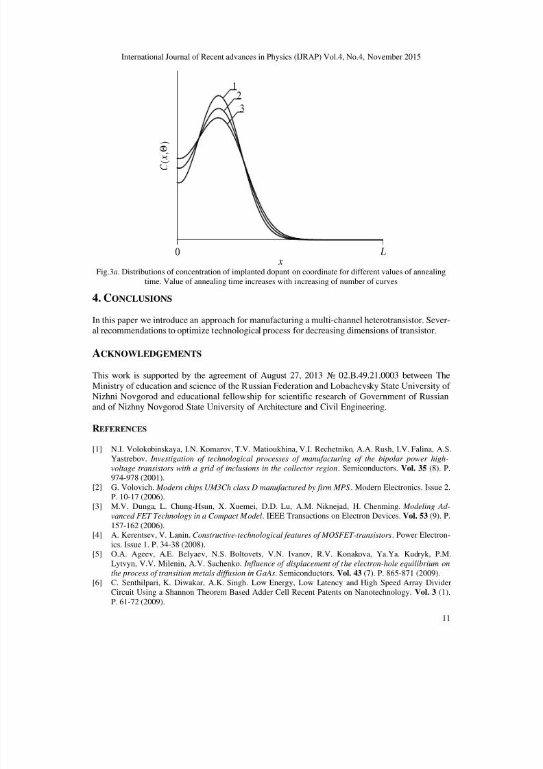
nealing time. Reason of the optimization is too large diffusion depth of dopants from channels oftransistors into nearest materials. Figs. 3 are illustrations of this situations. We used recently in-
troduced criterion [9,10,18-24] to determine optimal value of annealing time. Framework the cri-terion we approximate real distribution of concentration of dopant by idealized step-wise function
ψ ( x, y, z). Framework the criterion we minimize the following mean-squared error to determine theoptimal value of annealing time
( ) ( )[ ]∫ ∫ ∫ −Θ= x y z L L L
z y x
xd yd zd z y x z y xC L L L
U 0 0 0
,,,,,1
ψ . (18)

7/23/2019 On Optimization of Manufacturing of Multichannel Heterotransistors to Increase Their Integration Rate
http://slidepdf.com/reader/full/on-optimization-of-manufacturing-of-multichannel-heterotransistors-to-increase 10/14
International Journal of Recent advances in Physics (IJRAP) Vol.4, No.4, November 2015
10
x
0.0
0.5
1.0
1.5
C ( x ,
Θ
)
12
34
56
0 L /4 L /2 3 L /4 L
Interface
n or p channelim epitaxial layer
Fig. 2a. Spatial distributions of concentrations of infused dopant. Coordinate x is perpendicular to interface
between layers of heterostructure. Difference between values of dopant diffusion coefficient in layers of
heterostructure increases with increasing of number of distributions.
x
0.0
0.5
1.0
1.5
2.0
C ( x ,
Θ )
23
4
1
0 L /4 L /2 3 L /4 L
n or p channelim epitaxial layer
Fig. 2b. Spatial distributions of concentrations of infused dopant. Distributions 1 and 2 have been calculat-
ed in homogenous material for two values of annealing time (Θ =0,0048( L x2+ L y
2+ L z
2)/ D0 and Θ =0,0057
( L x2
+ L y2+ L z
2)/ D0, respectively). Distributions 3 and 4 have been calculated for heterostructure with two
layers for the same annealing time
The considered distributions in Figs. 2 corresponds exactly to compromise annealing time.
C ( x ,
Θ )
0 L x
1
2
3
Fig.3a. Distributions of concentration of infused dopant on coordinate for different values of annealing
time. Value of annealing time increases with increasing of number of curves
7/23/2019 On Optimization of Manufacturing of Multichannel Heterotransistors to Increase Their Integration Rate
http://slidepdf.com/reader/full/on-optimization-of-manufacturing-of-multichannel-heterotransistors-to-increase 11/14
International Journal of Recent advances in Physics (IJRAP) Vol.4, No.4, November 2015
11
x
C (
x ,
Θ )
12
3
0 L
Fig.3a. Distributions of concentration of implanted dopant on coordinate for different values of annealingtime. Value of annealing time increases with increasing of number of curves
4. CONCLUSIONS
In this paper we introduce an approach for manufacturing a multi-channel heterotransistor. Sever-al recommendations to optimize technological process for decreasing dimensions of transistor.
ACKNOWLEDGEMENTS
This work is supported by the agreement of August 27, 2013 № 02.В.49.21.0003 between The
Ministry of education and science of the Russian Federation and Lobachevsky State University of
Nizhni Novgorod and educational fellowship for scientific research of Government of Russian
and of Nizhny Novgorod State University of Architecture and Civil Engineering.
REFERENCES
[1] N.I. Volokobinskaya, I.N. Komarov, T.V. Matioukhina, V.I. Rechetniko, A.A. Rush, I.V. Falina, A.S.
Yastrebov. Investigation of technological processes of manufacturing of the bipolar power high-
voltage transistors with a grid of inclusions in the collector region. Semiconductors. Vol. 35 (8). P.
974-978 (2001).
[2] G. Volovich. Modern chips UM3Ch class D manufactured by firm MPS . Modern Electronics. Issue 2.
P. 10-17 (2006).
[3] M.V. Dunga, L. Chung-Hsun, X. Xuemei, D.D. Lu, A.M. Niknejad, H. Chenming. Modeling Ad-
vanced FET Technology in a Compact Model. IEEE Transactions on Electron Devices. Vol. 53 (9). P.
157-162 (2006).
[4] A. Kerentsev, V. Lanin. Constructive-technological features of MOSFET-transistors. Power Electron-ics. Issue 1. P. 34-38 (2008).
[5] O.A. Ageev, A.E. Belyaev, N.S. Boltovets, V.N. Ivanov, R.V. Konakova, Ya.Ya. Kudryk, P.M.
Lytvyn, V.V. Milenin, A.V. Sachenko. Influence of displacement of the electron-hole equilibrium on
the process of transition metals diffusion in GaAs. Semiconductors. Vol. 43 (7). P. 865-871 (2009).
[6] C. Senthilpari, K. Diwakar, A.K. Singh. Low Energy, Low Latency and High Speed Array Divider
Circuit Using a Shannon Theorem Based Adder Cell Recent Patents on Nanotechnology. Vol. 3 (1).
P. 61-72 (2009).
7/23/2019 On Optimization of Manufacturing of Multichannel Heterotransistors to Increase Their Integration Rate
http://slidepdf.com/reader/full/on-optimization-of-manufacturing-of-multichannel-heterotransistors-to-increase 12/14
International Journal of Recent advances in Physics (IJRAP) Vol.4, No.4, November 2015
12
[7] K.K. Ong, K.L. Pey, P.S. Lee, A.T.S. Wee, X.C. Wang, Y.F. Chong. Dopant distribution in the re-
crystallization transient at the maximum melt depth induced by laser annealing . Appl. Phys. Lett. 89
(17), 172111-172114 (2006).
[8] H.T. Wang, L.S. Tan, E. F. Chor. Pulsed laser annealing of Be-implanted GaN . J. Appl. Phys. Vol.
98 (9), 094901-094905 (2006).
[9] E.L. Pankratov. Redistribution of dopant during annealing of radiative defects in a multilayer struc-
ture by laser scans for production an implanted-junction rectifiers. Int. J. Nanoscience. Vol. 7 (4-5). P.187–197 (2008).
[10] E.L. Pankratov. Decreasing of depth of implanted-junction rectifier in semiconductor heterostructure
by optimized laser annealing. J. Comp. Theor. Nanoscience. Vol. 7 (1). P. 289-295 (2010).
[11] Yu.V. Bykov, A.G. Yeremeev, N.A. Zharova, I.V. Plotnikov, K.I. Rybakov, M.N. Drozdov, Yu.N.
Drozdov, V.D. Skupov. Diffusion processes in semiconductor structures during microwave anneal-
ing. Radiophysics and Quantum Electronics. Vol. 43 (8-9). P. 749-755 (2003).
[12] H. Ryssel, I. Ruge. Ion implantation. B.G. Teubner, Stuttgart, 1978.
[13] V.L. Vinetskiy, G.A. Kholodar', Radiative physics of semiconductors. "Naukova Dumka", Kiev,
1979, in Russian.
[14] Z.Yu. Gotra. Technology of microelectronic devices (Radio and communication, Moscow, 1991).
[15] P.M. Fahey, P.B. Griffin, J.D. Plummer. Point defects and dopant diffusion in silicon. Rev. Mod. Phys.
1989. V. 61.№ 2. P. 289-388.
[16] Yu.D. Sokolov. About the definition of dynamic forces in the mine lifting. Applied Mechanics. Vol.1
(1). P. 23-35 (1955).[17] E.L. Pankratov. Dynamics of delta-dopant redistribution during heterostructure growth. The European
Physical Journal B. Vol. 57 (3). P. 251-256 (2007).
[18] E.L. Pankratov. Influence of mechanical stress in a multilayer structure on spatial distribution of do-
pants in implanted-junction and diffusion-junction rectifiers. Mod. Phys. Lett. B. Vol. 24 (9). P. 867-
895 (2010).
[19] E.L. Pankratov. Dopant Diffusion Dynamics and Optimal Diffusion Time as Influenced by Diffusion-
Coefficient Nonuniformity Russian Microelectronics. 2007. V.36 (1). P. 33-39.
[20] E.L. Pankratov. Redistribution of dopant during annealing of radiative defects in a multilayer struc-
ture by laser scans for production an implanted-junction rectifiers. Int. J. Nanoscience. Vol. 7 (4-5). P.187–197 (2008).
[21] E.L. Pankratov. Decreasing of depth of implanted-junction rectifier in semiconductor heterostructure
by optimized laser annealing. J. Comp. Theor. Nanoscience. Vol. 7 (1). P. 289-295 (2010).
[22] E.L. Pankratov, E.A. Bulaeva. Application of native inhomogeneities to increase compactness of verti-
cal field-effect transistors. J. Comp. Theor. Nanoscience.Vol. 10
(4). P. 888-893 (2013).[23] E.L. Pankratov, E.A. Bulaeva. An approach to manufacture of bipolar transistors in thin film struc-
tures. On the method of optimization. Int. J. Micro-Nano Scale Transp. Vol. 4 (1). P. 17-31 (2014).
[24] E.L. Pankratov, E.A. Bulaeva. Increasing of sharpness of diffusion-junction heterorectifier by using
radiation processing. Int. J. Nanoscience. Vol. 11 (5). P. 1250028-1250035 (2012).
Authors:
Pankratov Evgeny Leonidovich was born at 1977. From 1985 to 1995 he was educated in a secondary
school in Nizhny Novgorod. From 1995 to 2004 he was educated in Nizhny Novgorod State University:
from 1995 to 1999 it was bachelor course in Radiophysics, from 1999 to 2001 it was master course in
Radiophysics with specialization in Statistical Radiophysics, from 2001 to 2004 it was PhD course in
Radiophysics. From 2004 to 2008 E.L. Pankratov was a leading technologist in Institute for Physics of Mi-
crostructures. From 2008 to 2012 E.L. Pankratov was a senior lecture/Associate Professor of Nizhny Nov-
gorod State University of Architecture and Civil Engineering. Now E.L. Pankratov is in his Full Doctorcourse in Radiophysical Department of Nizhny Novgorod State University. He has 110 published papers in
area of his researches.
Bulaeva Elena Alexeevna was born at 1991. From 1997 to 2007 she was educated in secondary school of
village Kochunovo of Nizhny Novgorod region. From 2007 to 2009 she was educated in boarding school
“Center for gifted children”. From 2009 she is a student of Nizhny Novgorod State University of Architec-
ture and Civil Engineering (spatiality “Assessment and management of real estate”). At the same time she
7/23/2019 On Optimization of Manufacturing of Multichannel Heterotransistors to Increase Their Integration Rate
http://slidepdf.com/reader/full/on-optimization-of-manufacturing-of-multichannel-heterotransistors-to-increase 13/14
International Journal of Recent advances in Physics (IJRAP) Vol.4, No.4, November 2015
13
is a student of courses “Translator in the field of professional communication” and “Design (interior art)”
in the University. E.A. Bulaeva was a contributor of grant of President of Russia (grant № MK-
548.2010.2). She has 74 published papers in area of her researches.
APPENDIX
( ) ( ) ( ) ( )∫ ∫ ∫ ∫−ΘΘ
=
Θ
0 0 0 011, ,,,,,,,,,1
x y z L L L
jiba
z y x
abij t d xd yd zd t z y xV t z y x I T z y xk t L L L
A ,
( )2
0000
2
00
2
00
2
0042
VV II IV IV IV A A A A A B −−= , −++=
2
001000
3
0001
2
00003 IV II IV IV IV IV IV A A A A A A A B
( ) ( ) ( )[ ]−++−+++−− 121224 10100010010000010000
2
00 VV IV II II IV IV IV IV VV II IV A A A A A A A A A A A
2
000100
2
0000101024
IV IV IV IV II IV IV A A A A A A A +− , ( ){ ×−+++= 00
2
01
2
00
2
1001
2
002 1 II IV IV II IV IV
A A A A A A B
( ) ( +++
∫ ∫ ∫−−× 01000001000 0 0
2011 2,,1
4 IV IV IV IV IV
L L L
I
z y x
II IV A A A A A xd yd zd z y x f
L L L A A
x y z
)} ( ) ([{ ++−+++−+ 10100010010000010010100021224
VV IV II II IV IV IV IV II IV II IV A A A A A A A A A A A A
)] ( ) ( ) ( )
×−−∫ ∫ ∫+++++ 11200 0 0
100101
2
2,,2
121 IV VV
L L L
V
z y x
II IV IV A A xd yd zd z y x f L L L A A A
x y z
( )] ( ) ( )[ +++−+++++× 1212110100010010010010100 VV IV II II IV IV II IV IV II A A A A A A A A A A
]}0001
2 IV IV A A+ , ( ) [ −−−++=2011000100
2
100101001812 II IV II IV IV II IV IV IV A A A A A A A A A B
( ) ( )×−+++
∫ ∫ ∫−
001010000100000 0 0 4,,
1 II IV II IV IV IV IV
L L L
I z y x
A A A A A A A xd yd zd z y x f L L L
x y z
( ) ( ) ( )
×−−+++∫ ∫ ∫−×
11201001010 0 0
002
011,,
22
IV VV II IV IV
L L L
I
z y x
II
IV A A A A A xd yd zd z y x f
L L L
A A
x y z
7/23/2019 On Optimization of Manufacturing of Multichannel Heterotransistors to Increase Their Integration Rate
http://slidepdf.com/reader/full/on-optimization-of-manufacturing-of-multichannel-heterotransistors-to-increase 14/14
International Journal of Recent advances in Physics (IJRAP) Vol.4, No.4, November 2015
14
( )] ( ) ( )[ +++−+++++× 12121210100010010010010100 VV IV II II IV IV II IV IV II A A A A A A A A A A
]00012 IV IV A A+ , ( ) −
−∫ ∫ ∫+= 11
0 0 020
201000 ,,14 IV
L L L
I
z y x
II IV II A xd yd zd z y x f
L L L A A A B
x y z
( ) ( ) ( )
+−−+++∫ ∫ ∫− 112000100101
0 0 0
00 21,,2
IV VV II II IV IV
L L L
V
z y x
II A A A A A A xd yd zd z y x f L L L
A x y z
( )] ( )2
1001
2
01
2
10010111 ++++++ II IV IV II IV IV A A A A A A , −+−+= 6
23 32 Bq pq y
3 32 q pq ++− , ( ) ( )
−+−−+= 031
221
2320
3
2 826
4278
1 B B B B B B B B Bq , 223 48 B B y A −+= ,
( ) 722823 2
2031 B B B B p −−= .