on mica at right
DESCRIPTION
Surface: Silicon Nitride with CdS nanowires Silicon oxide coated followed by APTES coating from Agarwal group. These surfaces have been in our hands for about 1 year. - PowerPoint PPT PresentationTRANSCRIPT
Surface: Silicon Nitride with CdS nanowires Silicon oxide coated followed by APTES coatingfrom Agarwal group. These surfaces have been in our hands for about 1 year.
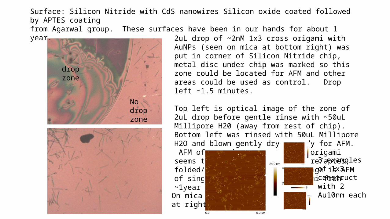
2uL drop of ~2nM 1x3 cross origami with AuNPs (seen on mica at bottom right) was put in corner of Silicon Nitride chip, metal disc under chip was marked so this zone could be located for AFM and other areas could be used as control. Drop left ~1.5 minutes.
Top left is optical image of the zone of 2uL drop before gentle rinse with ~50uL Millipore H20 (away from rest of chip). Bottom left was rinsed with 50uL Millipore H2O and blown gently dry – ready for AFM. AFM of one wire on next page, origami seems to not conform well on wire/aptes; folded/bunched? Also on next page is AFM of single (not 1x3) cross origami from ~1year ago.
On mica at right
drop zone
No drop zone
3 examples of 1x3 construct with 2 Au10nm each

At right is cross origmi imaged ~1year ago on similar sample. Coverage seems a bit more complete.
New AFM October 2014 below