old company name in catalogs and other documents electronics/r5f21332c… · r8c/33c group hardware...
TRANSCRIPT
To our customers,
Old Company Name in Catalogs and Other Documents
On April 1st, 2010, NEC Electronics Corporation merged with Renesas Technology
Corporation, and Renesas Electronics Corporation took over all the business of both companies. Therefore, although the old company name remains in this document, it is a valid Renesas Electronics document. We appreciate your understanding.
Renesas Electronics website: http://www.renesas.com
April 1st, 2010 Renesas Electronics Corporation
Issued by: Renesas Electronics Corporation (http://www.renesas.com)
Send any inquiries to http://www.renesas.com/inquiry.
Notice 1. All information included in this document is current as of the date this document is issued. Such information, however, is
subject to change without any prior notice. Before purchasing or using any Renesas Electronics products listed herein, please confirm the latest product information with a Renesas Electronics sales office. Also, please pay regular and careful attention to additional and different information to be disclosed by Renesas Electronics such as that disclosed through our website.
2. Renesas Electronics does not assume any liability for infringement of patents, copyrights, or other intellectual property rights of third parties by or arising from the use of Renesas Electronics products or technical information described in this document. No license, express, implied or otherwise, is granted hereby under any patents, copyrights or other intellectual property rights of Renesas Electronics or others.
3. You should not alter, modify, copy, or otherwise misappropriate any Renesas Electronics product, whether in whole or in part. 4. Descriptions of circuits, software and other related information in this document are provided only to illustrate the operation of
semiconductor products and application examples. You are fully responsible for the incorporation of these circuits, software, and information in the design of your equipment. Renesas Electronics assumes no responsibility for any losses incurred by you or third parties arising from the use of these circuits, software, or information.
5. When exporting the products or technology described in this document, you should comply with the applicable export control laws and regulations and follow the procedures required by such laws and regulations. You should not use Renesas Electronics products or the technology described in this document for any purpose relating to military applications or use by the military, including but not limited to the development of weapons of mass destruction. Renesas Electronics products and technology may not be used for or incorporated into any products or systems whose manufacture, use, or sale is prohibited under any applicable domestic or foreign laws or regulations.
6. Renesas Electronics has used reasonable care in preparing the information included in this document, but Renesas Electronics does not warrant that such information is error free. Renesas Electronics assumes no liability whatsoever for any damages incurred by you resulting from errors in or omissions from the information included herein.
7. Renesas Electronics products are classified according to the following three quality grades: “Standard”, “High Quality”, and “Specific”. The recommended applications for each Renesas Electronics product depends on the product’s quality grade, as indicated below. You must check the quality grade of each Renesas Electronics product before using it in a particular application. You may not use any Renesas Electronics product for any application categorized as “Specific” without the prior written consent of Renesas Electronics. Further, you may not use any Renesas Electronics product for any application for which it is not intended without the prior written consent of Renesas Electronics. Renesas Electronics shall not be in any way liable for any damages or losses incurred by you or third parties arising from the use of any Renesas Electronics product for an application categorized as “Specific” or for which the product is not intended where you have failed to obtain the prior written consent of Renesas Electronics. The quality grade of each Renesas Electronics product is “Standard” unless otherwise expressly specified in a Renesas Electronics data sheets or data books, etc.
“Standard”: Computers; office equipment; communications equipment; test and measurement equipment; audio and visual equipment; home electronic appliances; machine tools; personal electronic equipment; and industrial robots.
“High Quality”: Transportation equipment (automobiles, trains, ships, etc.); traffic control systems; anti-disaster systems; anti-crime systems; safety equipment; and medical equipment not specifically designed for life support.
“Specific”: Aircraft; aerospace equipment; submersible repeaters; nuclear reactor control systems; medical equipment or systems for life support (e.g. artificial life support devices or systems), surgical implantations, or healthcare intervention (e.g. excision, etc.), and any other applications or purposes that pose a direct threat to human life.
8. You should use the Renesas Electronics products described in this document within the range specified by Renesas Electronics, especially with respect to the maximum rating, operating supply voltage range, movement power voltage range, heat radiation characteristics, installation and other product characteristics. Renesas Electronics shall have no liability for malfunctions or damages arising out of the use of Renesas Electronics products beyond such specified ranges.
9. Although Renesas Electronics endeavors to improve the quality and reliability of its products, semiconductor products have specific characteristics such as the occurrence of failure at a certain rate and malfunctions under certain use conditions. Further, Renesas Electronics products are not subject to radiation resistance design. Please be sure to implement safety measures to guard them against the possibility of physical injury, and injury or damage caused by fire in the event of the failure of a Renesas Electronics product, such as safety design for hardware and software including but not limited to redundancy, fire control and malfunction prevention, appropriate treatment for aging degradation or any other appropriate measures. Because the evaluation of microcomputer software alone is very difficult, please evaluate the safety of the final products or system manufactured by you.
10. Please contact a Renesas Electronics sales office for details as to environmental matters such as the environmental compatibility of each Renesas Electronics product. Please use Renesas Electronics products in compliance with all applicable laws and regulations that regulate the inclusion or use of controlled substances, including without limitation, the EU RoHS Directive. Renesas Electronics assumes no liability for damages or losses occurring as a result of your noncompliance with applicable laws and regulations.
11. This document may not be reproduced or duplicated, in any form, in whole or in part, without prior written consent of Renesas Electronics.
12. Please contact a Renesas Electronics sales office if you have any questions regarding the information contained in this document or Renesas Electronics products, or if you have any other inquiries.
(Note 1) “Renesas Electronics” as used in this document means Renesas Electronics Corporation and also includes its majority-owned subsidiaries.
(Note 2) “Renesas Electronics product(s)” means any product developed or manufactured by or for Renesas Electronics.
R8C/33C GroupHardware Manual
16
User’s M
anual
Rev.1.00 2009.12
RENESAS MCUR8C FAMILY / R8C/3x SERIES
All information contained in these materials, including products and product specifications, represents information on the product at the time of publication and is subject to change by Renesas Electronics Corp. without notice. Please review the latest information published by Renesas Electronics Corp. through various means, including the Renesas Electronics Corp. website (http://www.renesas.com).

1. This document is provided for reference purposes only so that Renesas customers may select the appropriate Renesas products for their use. Renesas neither makes warranties or representations with respect to the accuracy or completeness of the information contained in this document nor grants any license to any intellectual property rights or any other rights of Renesas or any third party with respect to the information in this document. 2. Renesas shall have no liability for damages or infringement of any intellectual property or other rights arising out of the use of any information in this document, including, but not limited to, product data, diagrams, charts, programs, algorithms, and application circuit examples.3. You should not use the products or the technology described in this document for the purpose of military applications such as the development of weapons of mass destruction or for the purpose of any other military use. When exporting the products or technology described herein, you should follow the applicable export control laws and regulations, and procedures required by such laws and regulations.4. All information included in this document such as product data, diagrams, charts, programs, algorithms, and application circuit examples, is current as of the date this document is issued. Such information, however, is subject to change without any prior notice. Before purchasing or using any Renesas products listed in this document, please confirm the latest product information with a Renesas sales office. Also, please pay regular and careful attention to additional and different information to be disclosed by Renesas such as that disclosed through our website. (http://www.renesas.com )5. Renesas has used reasonable care in compiling the information included in this document, but Renesas assumes no liability whatsoever for any damages incurred as a result of errors or omissions in the information included in this document.6. When using or otherwise relying on the information in this document, you should evaluate the information in light of the total system before deciding about the applicability of such information to the intended application. Renesas makes no representations, warranties or guaranties regarding the suitability of its products for any particular application and specifically disclaims any liability arising out of the application and use of the information in this document or Renesas products. 7. With the exception of products specified by Renesas as suitable for automobile applications, Renesas products are not designed, manufactured or tested for applications or otherwise in systems the failure or malfunction of which may cause a direct threat to human life or create a risk of human injury or which require especially high quality and reliability such as safety systems, or equipment or systems for transportation and traffic, healthcare, combustion control, aerospace and aeronautics, nuclear power, or undersea communication transmission. If you are considering the use of our products for such purposes, please contact a Renesas sales office beforehand. Renesas shall have no liability for damages arising out of the uses set forth above.8. Notwithstanding the preceding paragraph, you should not use Renesas products for the purposes listed below: (1) artificial life support devices or systems (2) surgical implantations (3) healthcare intervention (e.g., excision, administration of medication, etc.) (4) any other purposes that pose a direct threat to human life Renesas shall have no liability for damages arising out of the uses set forth in the above and purchasers who elect to use Renesas products in any of the foregoing applications shall indemnify and hold harmless Renesas Technology Corp., its affiliated companies and their officers, directors, and employees against any and all damages arising out of such applications. 9. You should use the products described herein within the range specified by Renesas, especially with respect to the maximum rating, operating supply voltage range, movement power voltage range, heat radiation characteristics, installation and other product characteristics. Renesas shall have no liability for malfunctions or damages arising out of the use of Renesas products beyond such specified ranges.10. Although Renesas endeavors to improve the quality and reliability of its products, IC products have specific characteristics such as the occurrence of failure at a certain rate and malfunctions under certain use conditions. Please be sure to implement safety measures to guard against the possibility of physical injury, and injury or damage caused by fire in the event of the failure of a Renesas product, such as safety design for hardware and software including but not limited to redundancy, fire control and malfunction prevention, appropriate treatment for aging degradation or any other applicable measures. Among others, since the evaluation of microcomputer software alone is very difficult, please evaluate the safety of the final products or system manufactured by you. 11. In case Renesas products listed in this document are detached from the products to which the Renesas products are attached or affixed, the risk of accident such as swallowing by infants and small children is very high. You should implement safety measures so that Renesas products may not be easily detached from your products. Renesas shall have no liability for damages arising out of such detachment.12. This document may not be reproduced or duplicated, in any form, in whole or in part, without prior written approval from Renesas. 13. Please contact a Renesas sales office if you have any questions regarding the information contained in this document, Renesas semiconductor products, or if you have any other inquiries.
Notes regarding these materials

General Precautions in the Handling of MPU/MCU Products
The following usage notes are applicable to all MPU/MCU products from Renesas. For detailed usage notes on the products covered by this manual, refer to the relevant sections of the manual. If the descriptions under General Precautions in the Handling of MPU/MCU Products and in the body of the manual differ from each other, the description in the body of the manual takes precedence.
1. Handling of Unused Pins Handle unused pins in accord with the directions given under Handling of Unused Pins in the manual. The input pins of CMOS products are generally in the high-impedance state. In operation
with an unused pin in the open-circuit state, extra electromagnetic noise is induced in the vicinity of LSI, an associated shoot-through current flows internally, and malfunctions occur due to the false recognition of the pin state as an input signal become possible. Unused pins should be handled as described under Handling of Unused Pins in the manual.
2. Processing at Power-on The state of the product is undefined at the moment when power is supplied. The states of internal circuits in the LSI are indeterminate and the states of register
settings and pins are undefined at the moment when power is supplied. In a finished product where the reset signal is applied to the external reset pin, the states of pins are not guaranteed from the moment when power is supplied until the reset process is completed. In a similar way, the states of pins in a product that is reset by an on-chip power-on reset function are not guaranteed from the moment when power is supplied until the power reaches the level at which resetting has been specified.
3. Prohibition of Access to Reserved Addresses Access to reserved addresses is prohibited. The reserved addresses are provided for the possible future expansion of functions. Do
not access these addresses; the correct operation of LSI is not guaranteed if they are accessed.
4. Clock Signals After applying a reset, only release the reset line after the operating clock signal has become stable. When switching the clock signal during program execution, wait until the target clock signal has stabilized. When the clock signal is generated with an external resonator (or from an external
oscillator) during a reset, ensure that the reset line is only released after full stabilization of the clock signal. Moreover, when switching to a clock signal produced with an external resonator (or by an external oscillator) while program execution is in progress, wait until the target clock signal is stable.
5. Differences between Products Before changing from one product to another, i.e. to one with a different part number, confirm that the change will not lead to problems. The characteristics of MPU/MCU in the same group but having different part numbers may
differ because of the differences in internal memory capacity and layout pattern. When changing to products of different part numbers, implement a system-evaluation test for each of the products.

How to Use This Manual1. Purpose and Target Readers
This manual is designed to provide the user with an understanding of the hardware functions and electricalcharacteristics of the MCU. It is intended for users designing application systems incorporating the MCU. A basicknowledge of electric circuits, logical circuits, and MCUs is necessary in order to use this manual.The manual comprises an overview of the product; descriptions of the CPU, system control functions, peripheralfunctions, and electrical characteristics; and usage notes.
Particular attention should be paid to the precautionary notes when using the manual. These notes occurwithin the body of the text, at the end of each section, and in the Usage Notes section.
The revision history summarizes the locations of revisions and additions. It does not list all revisions. Referto the text of the manual for details.
The following documents apply to the R8C/33C Group. Make sure to refer to the latest versions of these documents.The newest versions of the documents listed may be obtained from the Renesas Technology Web site.
Document Type Description Document Title Document No.Shortsheet Hardware overview and electrical characteristics R8C/33C Group
ShortsheetREJ03B0284
Hardware manual Hardware specifications (pin assignments, memory maps, peripheral function specifications, electrical characteristics, timing charts) and operation descriptionNote: Refer to the application notes for details on using peripheral functions.
R8C/33C Group Hardware Manual
This hardware manual
Software manual Description of CPU instruction set R8C/Tiny Series Software Manual
REJ09B0001
Application note Information on using peripheral functions and application examplesSample programsInformation on writing programs in assembly language and C
Available from Renesas Technology Web site.
Renesas technical update
Product specifications, updates on documents, etc.

2. Notation of Numbers and SymbolsThe notation conventions for register names, bit names, numbers, and symbols used in this manual are describedbelow.
(1) Register Names, Bit Names, and Pin NamesRegisters, bits, and pins are referred to in the text by symbols. The symbol is accompanied by the word “register,”“bit,” or “pin” to distinguish the three categories.Examples the PM03 bit in the PM0 register
P3_5 pin, VCC pin
(2) Notation of NumbersThe indication “b” is appended to numeric values given in binary format. However, nothing is appended to thevalues of single bits. The indication “h” is appended to numeric values given in hexadecimal format. Nothing isappended to numeric values given in decimal format.Examples Binary: 11b
Hexadecimal: EFA0hDecimal: 1234

3. Register NotationThe symbols and terms used in register diagrams are described below.
x.x.x XXX Register (Symbol)
*1R/W: Read and write.R: Read only.W: Write only.−: Nothing is assigned.
*2• Reserved bit
Reserved bit. Set to specified value.
*3• Nothing is assigned.
Nothing is assigned to the bit. As the bit may be used for future functions, if necessary, set to 0.• Do not set to a value.
Operation is not guaranteed when a value is set.• Function varies according to the operating mode.
The function of the bit varies with the peripheral function mode. Refer to the register diagram for informationon the individual modes.
Address XXXXhBit b7 b6 b5 b4 b3 b2 b1 b0
Symbol XXX7 XXX6 XXX5 XXX4 — — XXX1 XXX0After Reset 0 0 0 0 0 0 0 0
Bit Symbol Bit Name Function R/Wb0 XXX0 XXX bit b1 b0
0 0: XXX 0 1: XXX 1 0: Do not set. 1 1: XXX
R/Wb1 XXX1 R/W
b2 — Nothing is assigned. If necessary, set to 0. When read, the content is undefined. —b3 — Reserved bit Set to 0. R/Wb4 XXX4 XXX bit Function varies according to the operating mode. R/Wb5 XXX5 Wb6 XXX6 R/Wb7 XXX7 XXX bit 0: XXX
1: XXXR
*1
*2 *3

4. List of Abbreviations and Acronyms
All trademarks and registered trademarks are the property of their respective owners.
Abbreviation Full FormACIA Asynchronous Communication Interface Adapterbps bits per secondCRC Cyclic Redundancy CheckDMA Direct Memory AccessDMAC Direct Memory Access ControllerGSM Global System for Mobile CommunicationsHi-Z High ImpedanceIEBus Inter Equipment BusI/O Input/OutputIrDA Infrared Data AssociationLSB Least Significant BitMSB Most Significant BitNC Non-ConnectPLL Phase Locked LoopPWM Pulse Width ModulationSIM Subscriber Identity ModuleUART Universal Asynchronous Receiver/TransmitterVCO Voltage Controlled Oscillator

A - 1
SFR Page Reference ........................................................................................................................... B - 1
1. Overview ......................................................................................................................................... 11.1 Features ..................................................................................................................................................... 1
1.1.1 Applications .......................................................................................................................................... 11.1.2 Specifications ........................................................................................................................................ 2
1.2 Product List ............................................................................................................................................... 41.3 Block Diagram ......................................................................................................................................... 51.4 Pin Assignment .......................................................................................................................................... 61.5 Pin Functions ............................................................................................................................................. 8
2. Central Processing Unit (CPU) ..................................................................................................... 102.1 Data Registers (R0, R1, R2, and R3) ...................................................................................................... 112.2 Address Registers (A0 and A1) ............................................................................................................... 112.3 Frame Base Register (FB) ....................................................................................................................... 112.4 Interrupt Table Register (INTB) .............................................................................................................. 112.5 Program Counter (PC) ............................................................................................................................. 112.6 User Stack Pointer (USP) and Interrupt Stack Pointer (ISP) .................................................................. 112.7 Static Base Register (SB) ........................................................................................................................ 112.8 Flag Register (FLG) ................................................................................................................................ 11
2.8.1 Carry Flag (C) ..................................................................................................................................... 112.8.2 Debug Flag (D) ................................................................................................................................... 112.8.3 Zero Flag (Z) ....................................................................................................................................... 112.8.4 Sign Flag (S) ....................................................................................................................................... 112.8.5 Register Bank Select Flag (B) ............................................................................................................ 112.8.6 Overflow Flag (O) .............................................................................................................................. 112.8.7 Interrupt Enable Flag (I) ..................................................................................................................... 122.8.8 Stack Pointer Select Flag (U) .............................................................................................................. 122.8.9 Processor Interrupt Priority Level (IPL) ............................................................................................. 122.8.10 Reserved Bit ........................................................................................................................................ 12
3. Memory ......................................................................................................................................... 133.1 R8C/33C Group ....................................................................................................................................... 13
4. Special Function Registers (SFRs) ............................................................................................... 14
5. Resets ........................................................................................................................................... 265.1 Registers .................................................................................................................................................. 28
5.1.1 Processor Mode Register 0 (PM0) ...................................................................................................... 285.1.2 Reset Source Determination Register (RSTFR) ................................................................................. 285.1.3 Option Function Select Register (OFS) .............................................................................................. 295.1.4 Option Function Select Register 2 (OFS2) ......................................................................................... 30
5.2 Hardware Reset ....................................................................................................................................... 315.2.1 When Power Supply is Stable ............................................................................................................. 315.2.2 Power On ............................................................................................................................................ 31
5.3 Power-On Reset Function ....................................................................................................................... 335.4 Voltage Monitor 0 Reset ......................................................................................................................... 345.5 Watchdog Timer Reset ............................................................................................................................ 355.6 Software Reset ......................................................................................................................................... 35
Table of Contents

A - 2
5.7 Cold Start-Up/Warm Start-Up Determination Function ......................................................................... 365.8 Reset Source Determination Function ..................................................................................................... 36
6. Voltage Detection Circuit .............................................................................................................. 376.1 Overview ................................................................................................................................................. 376.2 Registers .................................................................................................................................................. 41
6.2.1 Voltage Monitor Circuit Control Register (CMPA) ........................................................................... 416.2.2 Voltage Monitor Circuit Edge Select Register (VCAC) .................................................................... 426.2.3 Voltage Detect Register 1 (VCA1) ..................................................................................................... 426.2.4 Voltage Detect Register 2 (VCA2) ..................................................................................................... 436.2.5 Voltage Detection 1 Level Select Register (VD1LS) ......................................................................... 446.2.6 Voltage Monitor 0 Circuit Control Register (VW0C) ........................................................................ 456.2.7 Voltage Monitor 1 Circuit Control Register (VW1C) ........................................................................ 466.2.8 Voltage Monitor 2 Circuit Control Register (VW2C) ........................................................................ 476.2.9 Option Function Select Register (OFS) .............................................................................................. 48
6.3 VCC Input Voltage .................................................................................................................................. 496.3.1 Monitoring Vdet0 ............................................................................................................................... 496.3.2 Monitoring Vdet1 ............................................................................................................................... 496.3.3 Monitoring Vdet2 ............................................................................................................................... 49
6.4 Voltage Monitor 0 Reset ......................................................................................................................... 506.5 Voltage Monitor 1 Interrupt .................................................................................................................... 516.6 Voltage Monitor 2 Interrupt .................................................................................................................... 53
7. I/O Ports ........................................................................................................................................ 557.1 Functions of I/O Ports ............................................................................................................................. 557.2 Effect on Peripheral Functions ................................................................................................................ 567.3 Pins Other than I/O Ports ......................................................................................................................... 567.4 Registers .................................................................................................................................................. 68
7.4.1 Port Pi Direction Register (PDi) (i = 0 to 4) ....................................................................................... 687.4.2 Port Pi Register (Pi) (i = 0 to 4) .......................................................................................................... 697.4.3 Timer RA Pin Select Register (TRASR) ............................................................................................ 707.4.4 Timer RB/RC Pin Select Register (TRBRCSR) ................................................................................. 707.4.5 Timer RC Pin Select Register 0 (TRCPSR0) ..................................................................................... 717.4.6 Timer RC Pin Select Register 1 (TRCPSR1) ..................................................................................... 727.4.7 UART0 Pin Select Register (U0SR) ................................................................................................... 737.4.8 UART1 Pin Select Register (U1SR) ................................................................................................... 737.4.9 UART2 Pin Select Register 0 (U2SR0) .............................................................................................. 747.4.10 UART2 Pin Select Register 1 (U2SR1) .............................................................................................. 747.4.11 SSU/IIC Pin Select Register (SSUIICSR) .......................................................................................... 757.4.12 INT Interrupt Input Pin Select Register (INTSR) ............................................................................... 757.4.13 I/O Function Pin Select Register (PINSR) ......................................................................................... 767.4.14 Pull-Up Control Register 0 (PUR0) .................................................................................................... 777.4.15 Pull-Up Control Register 1 (PUR1) .................................................................................................... 777.4.16 Port P1 Drive Capacity Control Register (P1DRR) ............................................................................ 787.4.17 Port P2 Drive Capacity Control Register (P2DRR) ............................................................................ 787.4.18 Drive Capacity Control Register 0 (DRR0) ........................................................................................ 797.4.19 Drive Capacity Control Register 1 (DRR1) ........................................................................................ 807.4.20 Input Threshold Control Register 0 (VLT0) ....................................................................................... 817.4.21 Input Threshold Control Register 1 (VLT1) ....................................................................................... 82

A - 3
7.5 Port Settings ............................................................................................................................................ 837.6 Unassigned Pin Handling ........................................................................................................................ 96
8. Bus ................................................................................................................................................ 97
9. Clock Generation Circuit ............................................................................................................... 999.1 Overview ................................................................................................................................................. 999.2 Registers ................................................................................................................................................ 102
9.2.1 System Clock Control Register 0 (CM0) .......................................................................................... 1029.2.2 System Clock Control Register 1 (CM1) .......................................................................................... 1039.2.3 System Clock Control Register 3 (CM3) .......................................................................................... 1049.2.4 Oscillation Stop Detection Register (OCD) ...................................................................................... 1059.2.5 High-Speed On-Chip Oscillator Control Register 7 (FRA7) ............................................................ 1059.2.6 High-Speed On-Chip Oscillator Control Register 0 (FRA0) ............................................................ 1069.2.7 High-Speed On-Chip Oscillator Control Register 1 (FRA1) ............................................................ 1069.2.8 High-Speed On-Chip Oscillator Control Register 2 (FRA2) ............................................................ 1079.2.9 Clock Prescaler Reset Flag (CPSRF) ................................................................................................ 1079.2.10 High-Speed On-Chip Oscillator Control Register 4 (FRA4) ............................................................ 1089.2.11 High-Speed On-Chip Oscillator Control Register 5 (FRA5) ............................................................ 1089.2.12 High-Speed On-Chip Oscillator Control Register 6 (FRA6) ............................................................ 1089.2.13 High-Speed On-Chip Oscillator Control Register 3 (FRA3) ............................................................ 1089.2.14 Voltage Detect Register 2 (VCA2) ................................................................................................... 109
9.3 XIN Clock ............................................................................................................................................. 1119.4 On-Chip Oscillator Clock ...................................................................................................................... 112
9.4.1 Low-Speed On-Chip Oscillator Clock .............................................................................................. 1129.4.2 High-Speed On-Chip Oscillator Clock ............................................................................................. 112
9.5 XCIN Clock ........................................................................................................................................... 1139.6 CPU Clock and Peripheral Function Clock ........................................................................................... 114
9.6.1 System Clock .................................................................................................................................... 1149.6.2 CPU Clock ........................................................................................................................................ 1149.6.3 Peripheral Function Clock (f1, f2, f4, f8, and f32) ........................................................................... 1149.6.4 fOCO ................................................................................................................................................. 1149.6.5 fOCO40M ......................................................................................................................................... 1149.6.6 fOCO-F ............................................................................................................................................. 1149.6.7 fOCO-S ............................................................................................................................................. 1159.6.8 fOCO128 ........................................................................................................................................... 1159.6.9 fC, fC4, and fC32 .............................................................................................................................. 1159.6.10 fOCO-WDT ...................................................................................................................................... 115
9.7 Power Control ........................................................................................................................................ 1169.7.1 Standard Operating Mode ................................................................................................................. 1169.7.2 Wait Mode ........................................................................................................................................ 1189.7.3 Stop Mode ......................................................................................................................................... 122
9.8 Oscillation Stop Detection Function ..................................................................................................... 1259.8.1 How to Use Oscillation Stop Detection Function ............................................................................. 126
9.9 Notes on Clock Generation Circuit ....................................................................................................... 1299.9.1 Stop Mode ......................................................................................................................................... 1299.9.2 Wait Mode ........................................................................................................................................ 1299.9.3 Oscillation Stop Detection Function ................................................................................................. 1309.9.4 Oscillation Circuit Constants ............................................................................................................ 130

A - 4
10. Protection .................................................................................................................................... 13110.1 Register .................................................................................................................................................. 131
10.1.1 Protect Register (PRCR) ................................................................................................................... 131
11. Interrupts ..................................................................................................................................... 13211.1 Overview ............................................................................................................................................... 132
11.1.1 Types of Interrupts ............................................................................................................................ 13211.1.2 Software Interrupts ........................................................................................................................... 13311.1.3 Special Interrupts .............................................................................................................................. 13411.1.4 Peripheral Function Interrupts .......................................................................................................... 13411.1.5 Interrupts and Interrupt Vectors ........................................................................................................ 135
11.2 Registers ................................................................................................................................................ 13611.2.1 Interrupt Control Register
(TREIC, S2TIC, S2RIC, KUPIC, ADIC, S0TIC, S0RIC, S1TIC, S1RIC, TRAIC, TRBIC, U2BCNIC, VCMP1IC, VCMP2IC) .................................................................................................................... 137
11.2.2 Interrupt Control Register (FMRDYIC, TRCIC, SSUIC/IICIC) ..................................................... 13811.2.3 INTi Interrupt Control Register (INTiIC) (i = 0, 1, 3) ...................................................................... 139
11.3 Interrupt Control .................................................................................................................................... 14011.3.1 I Flag ................................................................................................................................................. 14011.3.2 IR Bit ................................................................................................................................................. 14011.3.3 Bits ILVL2 to ILVL0, IPL ................................................................................................................ 14011.3.4 Interrupt Sequence ............................................................................................................................ 14111.3.5 Interrupt Response Time ................................................................................................................... 14211.3.6 IPL Change when Interrupt Request is Acknowledged .................................................................... 14211.3.7 Saving Registers ............................................................................................................................... 14311.3.8 Returning from Interrupt Routine ..................................................................................................... 14511.3.9 Interrupt Priority ............................................................................................................................... 14511.3.10 Interrupt Priority Level Selection Circuit ......................................................................................... 146
11.4 INT Interrupt ......................................................................................................................................... 14711.4.1 INTi Interrupt (i = 0, 1, 3) ................................................................................................................. 14711.4.2 INT Interrupt Input Pin Select Register (INTSR) ............................................................................. 14711.4.3 External Input Enable Register 0 (INTEN) ...................................................................................... 14811.4.4 INT Input Filter Select Register 0 (INTF) ........................................................................................ 14811.4.5 INTi Input Filter (i = 0, 1, 3) ............................................................................................................. 149
11.5 Key Input Interrupt ................................................................................................................................ 15011.5.1 Key Input Enable Register 0 (KIEN) ................................................................................................ 151
11.6 Address Match Interrupt ........................................................................................................................ 15211.6.1 Address Match Interrupt Enable Register i (AIERi) (i = 0 or 1) ...................................................... 15311.6.2 Address Match Interrupt Register i (RMADi) (i = 0 or 1) ................................................................ 153
11.7 Timer RC Interrupt, Synchronous Serial Communication Unit Interrupt, I2C bus Interface Interrupt, and Flash Memory Interrupt (Interrupts with Multiple Interrupt Request Sources) .................................... 154
11.8 Notes on Interrupts ................................................................................................................................ 15611.8.1 Reading Address 00000h .................................................................................................................. 15611.8.2 SP Setting .......................................................................................................................................... 15611.8.3 External Interrupt and Key Input Interrupt ....................................................................................... 15611.8.4 Changing Interrupt Sources .............................................................................................................. 15711.8.5 Rewriting Interrupt Control Register ................................................................................................ 158

A - 5
12. ID Code Areas ............................................................................................................................ 15912.1 Overview ............................................................................................................................................... 15912.2 Functions ............................................................................................................................................... 16012.3 Forced Erase Function ........................................................................................................................... 16112.4 Standard Serial I/O Mode Disabled Function ....................................................................................... 16112.5 Notes on ID Code Areas ........................................................................................................................ 162
12.5.1 Setting Example of ID Code Areas ................................................................................................... 162
13. Option Function Select Area ....................................................................................................... 16313.1 Overview ............................................................................................................................................... 16313.2 Registers ................................................................................................................................................ 164
13.2.1 Option Function Select Register (OFS) ............................................................................................ 16413.2.2 Option Function Select Register 2 (OFS2) ....................................................................................... 165
13.3 Notes on Option Function Select Area .................................................................................................. 16613.3.1 Setting Example of Option Function Select Area ............................................................................. 166
14. Watchdog Timer ......................................................................................................................... 16714.1 Overview ............................................................................................................................................... 16714.2 Registers ................................................................................................................................................ 169
14.2.1 Processor Mode Register 1 (PM1) .................................................................................................... 16914.2.2 Watchdog Timer Reset Register (WDTR) ........................................................................................ 16914.2.3 Watchdog Timer Start Register (WDTS) ......................................................................................... 16914.2.4 Watchdog Timer Control Register (WDTC) .................................................................................... 17014.2.5 Count Source Protection Mode Register (CSPR) ............................................................................. 17014.2.6 Option Function Select Register (OFS) ............................................................................................ 17114.2.7 Option Function Select Register 2 (OFS2) ....................................................................................... 172
14.3 Functional Description ......................................................................................................................... 17314.3.1 Common Items for Multiple Modes ................................................................................................. 17314.3.2 Count Source Protection Mode Disabled .......................................................................................... 17414.3.3 Count Source Protection Mode Enabled ........................................................................................... 175
15. DTC ............................................................................................................................................ 17615.1 Overview ............................................................................................................................................... 17615.2 Registers ................................................................................................................................................ 177
15.2.1 DTC Control Register j (DTCCRj) (j = 0 to 23) ............................................................................... 17815.2.2 DTC Block Size Register j (DTBLSj) (j = 0 to 23) .......................................................................... 17815.2.3 DTC Transfer Count Register j (DTCCTj) (j = 0 to 23) ................................................................... 17915.2.4 DTC Transfer Count Reload Register j (DTRLDj) (j = 0 to 23) ...................................................... 17915.2.5 DTC Source Address Register j (DTSARj) (j = 0 to 23) .................................................................. 17915.2.6 DTC Destination Address Register j (DTDARj) (j = 0 to 23) .......................................................... 17915.2.7 DTC Activation Enable Register i (DTCENi) (i = 0 to 3, 5, 6) ........................................................ 18015.2.8 DTC Activation Control Register (DTCTL) .................................................................................... 181
15.3 Function Description ............................................................................................................................. 18215.3.1 Overview ........................................................................................................................................... 18215.3.2 Activation Sources ............................................................................................................................ 18215.3.3 Control Data Allocation and DTC Vector Table .............................................................................. 18415.3.4 Normal Mode .................................................................................................................................... 18915.3.5 Repeat Mode ..................................................................................................................................... 19015.3.6 Chain Transfers ................................................................................................................................. 191

A - 6
15.3.7 Interrupt Sources ............................................................................................................................... 19115.3.8 Operation Timings ............................................................................................................................ 19215.3.9 Number of DTC Execution Cycles ................................................................................................... 19315.3.10 DTC Activation Source Acknowledgement and Interrupt Source Flags .......................................... 194
15.4 Notes on DTC ........................................................................................................................................ 19615.4.1 DTC activation source ...................................................................................................................... 19615.4.2 DTCENi (i = 0 to 3, 5, 6) Registers .................................................................................................. 19615.4.3 Peripheral Modules ........................................................................................................................... 19615.4.4 Interrupt Request ............................................................................................................................... 196
16. General Overview of Timers ....................................................................................................... 197
17. Timer RA ..................................................................................................................................... 19917.1 Overview ............................................................................................................................................... 19917.2 Registers ................................................................................................................................................ 200
17.2.1 Timer RA Control Register (TRACR) .............................................................................................. 20017.2.2 Timer RA I/O Control Register (TRAIOC) ...................................................................................... 20017.2.3 Timer RA Mode Register (TRAMR) ................................................................................................ 20117.2.4 Timer RA Prescaler Register (TRAPRE) ......................................................................................... 20117.2.5 Timer RA Register (TRA) ................................................................................................................ 20217.2.6 Timer RA Pin Select Register (TRASR) .......................................................................................... 202
17.3 Timer Mode ........................................................................................................................................... 20317.3.1 Timer RA I/O Control Register (TRAIOC) in Timer Mode ............................................................ 20317.3.2 Timer Write Control during Count Operation .................................................................................. 204
17.4 Pulse Output Mode ................................................................................................................................ 20517.4.1 Timer RA I/O Control Register (TRAIOC) in Pulse Output Mode ................................................. 206
17.5 Event Counter Mode ............................................................................................................................. 20717.5.1 Timer RA I/O Control Register (TRAIOC) in Event Counter Mode ............................................... 208
17.6 Pulse Width Measurement Mode .......................................................................................................... 20917.6.1 Timer RA I/O Control Register (TRAIOC) in Pulse Width Measurement Mode ............................ 21017.6.2 Operating Example ........................................................................................................................... 211
17.7 Pulse Period Measurement Mode .......................................................................................................... 21217.7.1 Timer RA I/O Control Register (TRAIOC) in Pulse Period Measurement Mode ........................... 21317.7.2 Operating Example ........................................................................................................................... 214
17.8 Notes on Timer RA ............................................................................................................................... 215
18. Timer RB ..................................................................................................................................... 21618.1 Overview ............................................................................................................................................... 21618.2 Registers ................................................................................................................................................ 217
18.2.1 Timer RB Control Register (TRBCR) .............................................................................................. 21718.2.2 Timer RB One-Shot Control Register (TRBOCR) ........................................................................... 21718.2.3 Timer RB I/O Control Register (TRBIOC) ...................................................................................... 21818.2.4 Timer RB Mode Register (TRBMR) ................................................................................................ 21818.2.5 Timer RB Prescaler Register (TRBPRE) .......................................................................................... 21918.2.6 Timer RB Secondary Register (TRBSC) .......................................................................................... 21918.2.7 Timer RB Primary Register (TRBPR) .............................................................................................. 22018.2.8 Timer RB/RC Pin Select Register (TRBRCSR) ............................................................................... 220
18.3 Timer Mode ........................................................................................................................................... 22118.3.1 Timer RB I/O Control Register (TRBIOC) in Timer Mode ............................................................. 221

A - 7
18.3.2 Timer Write Control during Count Operation .................................................................................. 22218.4 Programmable Waveform Generation Mode ........................................................................................ 224
18.4.1 Timer RB I/O Control Register (TRBIOC) in Programmable Waveform Generation Mode .......... 22518.4.2 Operating Example ........................................................................................................................... 226
18.5 Programmable One-shot Generation Mode ........................................................................................... 22718.5.1 Timer RB I/O Control Register (TRBIOC) in Programmable One-Shot Generation Mode ............ 22818.5.2 Operating Example ........................................................................................................................... 22918.5.3 One-Shot Trigger Selection .............................................................................................................. 230
18.6 Programmable Wait One-Shot Generation Mode ................................................................................. 23118.6.1 Timer RB I/O Control Register (TRBIOC) in Programmable Wait One-Shot Generation Mode ... 23218.6.2 Operating Example ........................................................................................................................... 233
18.7 Notes on Timer RB ................................................................................................................................ 23418.7.1 Timer Mode ...................................................................................................................................... 23418.7.2 Programmable Waveform Generation Mode .................................................................................... 23418.7.3 Programmable One-shot Generation Mode ...................................................................................... 23518.7.4 Programmable Wait One-shot Generation Mode ............................................................................. 235
19. Timer RC .................................................................................................................................... 23619.1 Overview ............................................................................................................................................... 23619.2 Registers ................................................................................................................................................ 238
19.2.1 Module Standby Control Register (MSTCR) ................................................................................... 23919.2.2 Timer RC Mode Register (TRCMR) ................................................................................................ 23919.2.3 Timer RC Control Register 1 (TRCCR1) ......................................................................................... 24019.2.4 Timer RC Interrupt Enable Register (TRCIER) ............................................................................... 24019.2.5 Timer RC Status Register (TRCSR) ................................................................................................. 24119.2.6 Timer RC I/O Control Register 0 (TRCIOR0) ................................................................................. 24219.2.7 Timer RC I/O Control Register 1 (TRCIOR1) ................................................................................. 24219.2.8 Timer RC Counter (TRC) ................................................................................................................. 24319.2.9 Timer RC General Registers A, B, C, and D (TRCGRA, TRCGRB, TRCGRC, TRCGRD) .......... 24319.2.10 Timer RC Control Register 2 (TRCCR2) ......................................................................................... 24419.2.11 Timer RC Digital Filter Function Select Register (TRCDF) ............................................................ 24419.2.12 Timer RC Output Master Enable Register (TRCOER) .................................................................... 24519.2.13 Timer RC Trigger Control Register (TRCADCR) ........................................................................... 24519.2.14 Timer RB/RC Pin Select Register (TRBRCSR) ............................................................................... 24619.2.15 Timer RC Pin Select Register 0 (TRCPSR0) ................................................................................... 24719.2.16 Timer RC Pin Select Register 1 (TRCPSR1) ................................................................................... 248
19.3 Common Items for Multiple Modes ...................................................................................................... 24919.3.1 Count Source ..................................................................................................................................... 24919.3.2 Buffer Operation ............................................................................................................................... 25019.3.3 Digital Filter ...................................................................................................................................... 25219.3.4 Forced Cutoff of Pulse Output .......................................................................................................... 253
19.4 Timer Mode (Input Capture Function) .................................................................................................. 25519.4.1 Timer RC I/O Control Register 0 (TRCIOR0) for Input Capture Function ..................................... 25719.4.2 Timer RC I/O Control Register 1 (TRCIOR1) for Input Capture Function ..................................... 25819.4.3 Operating Example ........................................................................................................................... 259
19.5 Timer Mode (Output Compare Function) ............................................................................................. 26019.5.1 Timer RC Control Register 1 (TRCCR1) for Output Compare Function ........................................ 26219.5.2 Timer RC I/O Control Register 0 (TRCIOR0) for Output Compare Function ................................ 26319.5.3 Timer RC I/O Control Register 1 (TRCIOR1) for Output Compare Function ................................ 264

A - 8
19.5.4 Timer RC Control Register 2 (TRCCR2) for Output Compare Function ........................................ 26519.5.5 Operating Example ........................................................................................................................... 26619.5.6 Changing Output Pins in Registers TRCGRC and TRCGRD .......................................................... 267
19.6 PWM Mode ........................................................................................................................................... 26919.6.1 Timer RC Control Register 1 (TRCCR1) in PWM Mode ................................................................ 27119.6.2 Timer RC Control Register 2 (TRCCR2) in PWM Mode ................................................................ 27119.6.3 Operating Example ........................................................................................................................... 273
19.7 PWM2 Mode ......................................................................................................................................... 27519.7.1 Timer RC Control Register 1 (TRCCR1) in PWM2 Mode .............................................................. 27719.7.2 Timer RC Control Register 2 (TRCCR2) in PWM2 Mode .............................................................. 27819.7.3 Timer RC Digital Filter Function Select Register (TRCDF) in PWM2 Mode ................................. 27819.7.4 Operating Example ........................................................................................................................... 280
19.8 Timer RC Interrupt ................................................................................................................................ 28319.9 Notes on Timer RC ................................................................................................................................ 284
19.9.1 TRC Register .................................................................................................................................... 28419.9.2 TRCSR Register .............................................................................................................................. 28419.9.3 TRCCR1 Register ............................................................................................................................. 28419.9.4 Count Source Switching ................................................................................................................... 28419.9.5 Input Capture Function ..................................................................................................................... 28519.9.6 TRCMR Register in PWM2 Mode ................................................................................................... 28519.9.7 Count Source fOCO40M .................................................................................................................. 285
20. Timer RE ..................................................................................................................................... 28620.1 Overview ............................................................................................................................................... 28620.2 Real-Time Clock Mode ......................................................................................................................... 287
20.2.1 Timer RE Second Data Register (TRESEC) in Real-Time Clock Mode ......................................... 28920.2.2 Timer RE Minute Data Register (TREMIN) in Real-Time Clock Mode ......................................... 28920.2.3 Timer RE Hour Data Register (TREHR) in Real-Time Clock Mode ............................................... 29020.2.4 Timer RE Day of Week Data Register (TREWK) in Real-Time Clock Mode ................................ 29020.2.5 Timer RE Control Register 1 (TRECR1) in Real-Time Clock Mode .............................................. 29120.2.6 Timer RE Control Register 2 (TRECR2) in Real-Time Clock Mode .............................................. 29220.2.7 Timer RE Count Source Select Register (TRECSR) in Real-Time Clock Mode ............................. 29320.2.8 Operating Example ........................................................................................................................... 294
20.3 Output Compare Mode .......................................................................................................................... 29520.3.1 Timer RE Counter Data Register (TRESEC) in Output Compare Mode ......................................... 29720.3.2 Timer RE Compare Data Register (TREMIN) in Output Compare Mode ....................................... 29720.3.3 Timer RE Control Register 1 (TRECR1) in Output Compare Mode ............................................... 29820.3.4 Timer RE Control Register 2 (TRECR2) in Output Compare Mode ............................................... 29820.3.5 Timer RE Count Source Select Register (TRECSR) in Output Compare Mode .............................. 29920.3.6 Operating Example ........................................................................................................................... 300
20.4 Notes on Timer RE ................................................................................................................................ 30120.4.1 Starting and Stopping Count ............................................................................................................. 30120.4.2 Register Setting ................................................................................................................................. 30120.4.3 Time Reading Procedure of Real-Time Clock Mode ....................................................................... 303
21. Serial Interface (UARTi (i = 0 or 1)) ............................................................................................ 30421.1 Overview ............................................................................................................................................... 30421.2 Registers ................................................................................................................................................ 306
21.2.1 UARTi Transmit/Receive Mode Register (UiMR) (i = 0 or 1) ........................................................ 306

A - 9
21.2.2 UARTi Bit Rate Register (UiBRG) (i = 0 or 1) ................................................................................ 30621.2.3 UARTi Transmit Buffer Register (UiTB) (i = 0 or 1) ...................................................................... 30721.2.4 UARTi Transmit/Receive Control Register 0 (UiC0) (i = 0 or 1) .................................................... 30821.2.5 UARTi Transmit/Receive Control Register 1 (UiC1) (i = 0 or 1) .................................................... 30821.2.6 UARTi Receive Buffer Register (UiRB) (i = 0 or 1) ....................................................................... 30921.2.7 UART0 Pin Select Register (U0SR) ................................................................................................. 31021.2.8 UART1 Pin Select Register (U1SR) ................................................................................................. 310
21.3 Clock Synchronous Serial I/O Mode ..................................................................................................... 31121.3.1 Measure for Dealing with Communication Errors ........................................................................... 31521.3.2 Polarity Select Function .................................................................................................................... 31621.3.3 LSB First/MSB First Select Function ............................................................................................... 31621.3.4 Continuous Receive Mode ................................................................................................................ 317
21.4 Clock Asynchronous Serial I/O (UART) Mode .................................................................................... 31821.4.1 Bit Rate ............................................................................................................................................. 32321.4.2 Measure for Dealing with Communication Errors ........................................................................... 324
21.5 Notes on Serial Interface (UARTi (i = 0 or 1)) ..................................................................................... 325
22. Serial Interface (UART2) ............................................................................................................ 32622.1 Overview ............................................................................................................................................... 32622.2 Registers ................................................................................................................................................ 328
22.2.1 UART2 Transmit/Receive Mode Register (U2MR) ......................................................................... 32822.2.2 UART2 Bit Rate Register (U2BRG) ................................................................................................ 32822.2.3 UART2 Transmit Buffer Register (U2TB) ....................................................................................... 32922.2.4 UART2 Transmit/Receive Control Register 0 (U2C0) .................................................................... 33022.2.5 UART2 Transmit/Receive Control Register 1 (U2C1) .................................................................... 33122.2.6 UART2 Receive Buffer Register (U2RB) ........................................................................................ 33222.2.7 UART2 Digital Filter Function Select Register (URXDF) .............................................................. 33322.2.8 UART2 Special Mode Register 5 (U2SMR5) .................................................................................. 33322.2.9 UART2 Special Mode Register 4 (U2SMR4) .................................................................................. 33422.2.10 UART2 Special Mode Register 3 (U2SMR3) .................................................................................. 33422.2.11 UART2 Special Mode Register 2 (U2SMR2) .................................................................................. 33522.2.12 UART2 Special Mode Register (U2SMR) ....................................................................................... 33522.2.13 UART2 Pin Select Register 0 (U2SR0) ............................................................................................ 33622.2.14 UART2 Pin Select Register 1 (U2SR1) ............................................................................................ 336
22.3 Clock Synchronous Serial I/O Mode ..................................................................................................... 33722.3.1 Measure for Dealing with Communication Errors ........................................................................... 34122.3.2 CLK Polarity Select Function ........................................................................................................... 34122.3.3 LSB First/MSB First Select Function ............................................................................................... 34222.3.4 Continuous Receive Mode ................................................................................................................ 34222.3.5 Serial Data Logic Switching Function .............................................................................................. 34322.3.6 CTS/RTS Function ........................................................................................................................... 343
22.4 Clock Asynchronous Serial I/O (UART) Mode .................................................................................... 34422.4.1 Bit Rate ............................................................................................................................................. 34822.4.2 Measure for Dealing with Communication Errors ........................................................................... 34922.4.3 LSB First/MSB First Select Function ............................................................................................... 34922.4.4 Serial Data Logic Switching Function .............................................................................................. 35022.4.5 TXD and RXD I/O Polarity Inverse Function .................................................................................. 35022.4.6 CTS/RTS Function ........................................................................................................................... 35122.4.7 RXD2 Digital Filter Select Function ................................................................................................ 351

A - 10
22.5 Special Mode 1 (I2C Mode) .................................................................................................................. 35222.5.1 Detection of Start and Stop Conditions ............................................................................................ 35822.5.2 Output of Start and Stop Conditions ................................................................................................. 35922.5.3 Transfer Clock .................................................................................................................................. 36022.5.4 SDA Output ...................................................................................................................................... 36022.5.5 SDA Input ......................................................................................................................................... 36122.5.6 ACK and NACK ............................................................................................................................... 36122.5.7 Initialization of Transmission/Reception .......................................................................................... 361
22.6 Multiprocessor Communication Function ............................................................................................. 36222.6.1 Multiprocessor Transmission ............................................................................................................ 36522.6.2 Multiprocessor Reception ................................................................................................................. 36622.6.3 RXD2 Digital Filter Select Function ................................................................................................ 368
22.7 Notes on Serial Interface (UART2) ....................................................................................................... 36922.7.1 Clock Synchronous Serial I/O Mode ................................................................................................ 36922.7.2 Special Mode 1 (I2C Mode) .............................................................................................................. 370
23. Clock Synchronous Serial Interface ............................................................................................ 37123.1 Mode Selection ...................................................................................................................................... 371
24. Synchronous Serial Communication Unit (SSU) ........................................................................ 37224.1 Overview ............................................................................................................................................... 37224.2 Registers ................................................................................................................................................ 374
24.2.1 Module Standby Control Register (MSTCR) ................................................................................... 37424.2.2 SSU/IIC Pin Select Register (SSUIICSR) ........................................................................................ 37524.2.3 SS Bit Counter Register (SSBR) ...................................................................................................... 37624.2.4 SS Transmit Data Register (SSTDR) ................................................................................................ 37624.2.5 SS Receive Data Register (SSRDR) ................................................................................................. 37724.2.6 SS Control Register H (SSCRH) ...................................................................................................... 37724.2.7 SS Control Register L (SSCRL) ....................................................................................................... 37824.2.8 SS Mode Register (SSMR) ............................................................................................................... 37924.2.9 SS Enable Register (SSER) .............................................................................................................. 38024.2.10 SS Status Register (SSSR) ................................................................................................................ 38124.2.11 SS Mode Register 2 (SSMR2) .......................................................................................................... 382
24.3 Common Items for Multiple Modes ...................................................................................................... 38324.3.1 Transfer Clock .................................................................................................................................. 38324.3.2 SS Shift Register (SSTRSR) ............................................................................................................. 38524.3.3 Interrupt Requests ............................................................................................................................. 38624.3.4 Communication Modes and Pin Functions ....................................................................................... 387
24.4 Clock Synchronous Communication Mode .......................................................................................... 38824.4.1 Initialization in Clock Synchronous Communication Mode ............................................................ 38824.4.2 Data Transmission ............................................................................................................................ 38924.4.3 Data Reception .................................................................................................................................. 391
24.5 Operation in 4-Wire Bus Communication Mode .................................................................................. 39524.5.1 Initialization in 4-Wire Bus Communication Mode ......................................................................... 39624.5.2 Data Transmission ............................................................................................................................ 39724.5.3 Data Reception .................................................................................................................................. 39924.5.4 SCS Pin Control and Arbitration ...................................................................................................... 401
24.6 Notes on Synchronous Serial Communication Unit .............................................................................. 402

A - 11
25. I2C bus Interface ......................................................................................................................... 40325.1 Overview ............................................................................................................................................... 40325.2 Registers ................................................................................................................................................ 406
25.2.1 Module Standby Control Register (MSTCR) ................................................................................... 40625.2.2 SSU/IIC Pin Select Register (SSUIICSR) ........................................................................................ 40725.2.3 I/O Function Pin Select Register (PINSR) ....................................................................................... 40825.2.4 IIC bus Transmit Data Register (ICDRT) ......................................................................................... 40925.2.5 IIC bus Receive Data Register (ICDRR) .......................................................................................... 40925.2.6 IIC bus Control Register 1 (ICCR1) ................................................................................................. 41025.2.7 IIC bus Control Register 2 (ICCR2) ................................................................................................. 41125.2.8 IIC bus Mode Register (ICMR) ........................................................................................................ 41225.2.9 IIC bus Interrupt Enable Register (ICIER) ....................................................................................... 41325.2.10 IIC bus Status Register (ICSR) ......................................................................................................... 41425.2.11 Slave Address Register (SAR) .......................................................................................................... 41525.2.12 IIC bus Shift Register (ICDRS) ........................................................................................................ 415
25.3 Common Items for Multiple Modes ...................................................................................................... 41625.3.1 Transfer Clock .................................................................................................................................. 41625.3.2 SDA Pin Digital Delay Selection ...................................................................................................... 41825.3.3 Interrupt Requests ............................................................................................................................. 419
25.4 I2C bus Interface Mode ......................................................................................................................... 42025.4.1 I2C bus Format ................................................................................................................................. 42025.4.2 Master Transmit Operation ............................................................................................................... 42125.4.3 Master Receive Operation ................................................................................................................ 42325.4.4 Slave Transmit Operation ................................................................................................................. 42625.4.5 Slave Receive Operation ................................................................................................................... 429
25.5 Clock Synchronous Serial Mode ........................................................................................................... 43125.5.1 Clock Synchronous Serial Format .................................................................................................... 43125.5.2 Transmit Operation ........................................................................................................................... 43225.5.3 Receive Operation ............................................................................................................................. 433
25.6 Examples of Register Setting ................................................................................................................ 43425.7 Noise Canceller ..................................................................................................................................... 43825.8 Bit Synchronization Circuit ................................................................................................................... 43925.9 Notes on I2C bus Interface .................................................................................................................... 440
26. Hardware LIN .............................................................................................................................. 44126.1 Overview ............................................................................................................................................... 44126.2 Input/Output Pins .................................................................................................................................. 44226.3 Registers ................................................................................................................................................ 443
26.3.1 LIN Control Register 2 (LINCR2) .................................................................................................... 44326.3.2 LIN Control Register (LINCR) ......................................................................................................... 44426.3.3 LIN Status Register (LINST) ............................................................................................................ 444
26.4 Function Description ............................................................................................................................. 44526.4.1 Master Mode ..................................................................................................................................... 44526.4.2 Slave Mode ....................................................................................................................................... 44826.4.3 Bus Collision Detection Function ..................................................................................................... 45226.4.4 Hardware LIN End Processing ......................................................................................................... 453
26.5 Interrupt Requests .................................................................................................................................. 45426.6 Notes on Hardware LIN ........................................................................................................................ 455
A - 12
27. A/D Converter ............................................................................................................................. 45627.1 Overview ............................................................................................................................................... 45627.2 Registers ................................................................................................................................................ 458
27.2.1 On-Chip Reference Voltage Control Register (OCVREFCR) ......................................................... 45827.2.2 A/D Register i (ADi) (i = 0 to 7) ...................................................................................................... 45927.2.3 A/D Mode Register (ADMOD) ........................................................................................................ 46027.2.4 A/D Input Select Register (ADINSEL) ............................................................................................ 46127.2.5 A/D Control Register 0 (ADCON0) ................................................................................................. 46227.2.6 A/D Control Register 1 (ADCON1) ................................................................................................. 463
27.3 Common Items for Multiple Modes ...................................................................................................... 46427.3.1 Input/Output Pins .............................................................................................................................. 46427.3.2 A/D Conversion Cycles .................................................................................................................... 46427.3.3 A/D Conversion Start Condition ....................................................................................................... 46627.3.4 A/D Conversion Result ..................................................................................................................... 46827.3.5 Low Current Consumption Function ................................................................................................ 46827.3.6 Extended Analog Input Pins ............................................................................................................. 46827.3.7 A/D Open-Circuit Detection Assist Function ................................................................................... 468
27.4 One-Shot Mode ..................................................................................................................................... 47027.5 Repeat Mode 0 ....................................................................................................................................... 47127.6 Repeat Mode 1 ....................................................................................................................................... 47227.7 Single Sweep Mode ............................................................................................................................... 47427.8 Repeat Sweep Mode .............................................................................................................................. 47627.9 Output Impedance of Sensor under A/D Conversion ............................................................................ 47827.10 Notes on A/D Converter ........................................................................................................................ 479
28. D/A Converter ............................................................................................................................. 48028.1 Overview ............................................................................................................................................... 48028.2 Registers ................................................................................................................................................ 482
28.2.1 D/Ai Register (DAi) (i = 0 or 1) ....................................................................................................... 48228.2.2 D/A Control Register (DACON) ...................................................................................................... 482
29. Comparator B ............................................................................................................................. 48329.1 Overview ............................................................................................................................................... 48329.2 Registers ................................................................................................................................................ 485
29.2.1 Comparator B Control Register (INTCMP) ..................................................................................... 48529.2.2 External Input Enable Register 0 (INTEN) ...................................................................................... 48529.2.3 INT Input Filter Select Register 0 (INTF) ........................................................................................ 486
29.3 Functional Description .......................................................................................................................... 48729.3.1 Comparator Bi Digital Filter (i = 1 or 3) .......................................................................................... 488
29.4 Comparator B1 and Comparator B3 Interrupts ..................................................................................... 489
30. Flash Memory ............................................................................................................................. 49030.1 Overview ............................................................................................................................................... 49030.2 Memory Map ......................................................................................................................................... 49130.3 Functions to Prevent Flash Memory from being Rewritten .................................................................. 492
30.3.1 ID Code Check Function .................................................................................................................. 49230.3.2 ROM Code Protect Function ............................................................................................................ 49330.3.3 Option Function Select Register (OFS) ............................................................................................ 493
30.4 CPU Rewrite Mode ............................................................................................................................... 494

A - 13
30.4.1 Flash Memory Status Register (FST) ............................................................................................... 49530.4.2 Flash Memory Control Register 0 (FMR0) ...................................................................................... 49730.4.3 Flash Memory Control Register 1 (FMR1) ...................................................................................... 49930.4.4 Flash Memory Control Register 2 (FMR2) ...................................................................................... 50130.4.5 EW0 Mode ........................................................................................................................................ 50330.4.6 EW1 Mode ........................................................................................................................................ 50330.4.7 Suspend Operation ............................................................................................................................ 50430.4.8 How to Set and Exit Each Mode ....................................................................................................... 50530.4.9 BGO (BackGround Operation) Function .......................................................................................... 50630.4.10 Data Protect Function ....................................................................................................................... 50730.4.11 Software Commands ......................................................................................................................... 50830.4.12 Full Status Check .............................................................................................................................. 518
30.5 Standard Serial I/O Mode ...................................................................................................................... 52030.5.1 ID Code Check Function .................................................................................................................. 520
30.6 Parallel I/O Mode .................................................................................................................................. 52330.6.1 ROM Code Protect Function ............................................................................................................ 523
30.7 Notes on Flash Memory ........................................................................................................................ 52430.7.1 CPU Rewrite Mode ........................................................................................................................... 524
31. Reducing Power Consumption ................................................................................................... 52831.1 Overview ............................................................................................................................................... 52831.2 Key Points and Processing Methods for Reducing Power Consumption ............................................. 528
31.2.1 Voltage Detection Circuit ................................................................................................................. 52831.2.2 Ports .................................................................................................................................................. 52831.2.3 Clocks ............................................................................................................................................... 52831.2.4 Wait Mode, Stop Mode ..................................................................................................................... 52831.2.5 Stopping Peripheral Function Clocks ............................................................................................... 52831.2.6 Timers ............................................................................................................................................... 52831.2.7 A/D Converter ................................................................................................................................... 52831.2.8 Clock Synchronous Serial Interface ................................................................................................. 52831.2.9 Reducing Internal Power Consumption ............................................................................................ 52931.2.10 Stopping Flash Memory .................................................................................................................... 53031.2.11 Low-Current-Consumption Read Mode ........................................................................................... 53131.2.12 Others ................................................................................................................................................ 532
32. Electrical Characteristics ............................................................................................................ 533
33. Usage Notes ............................................................................................................................... 56033.1 Notes on Clock Generation Circuit ....................................................................................................... 560
33.1.1 Stop Mode ......................................................................................................................................... 56033.1.2 Wait Mode ........................................................................................................................................ 56033.1.3 Oscillation Stop Detection Function ................................................................................................. 56133.1.4 Oscillation Circuit Constants ............................................................................................................ 561
33.2 Notes on Interrupts ................................................................................................................................ 56233.2.1 Reading Address 00000h .................................................................................................................. 56233.2.2 SP Setting .......................................................................................................................................... 56233.2.3 External Interrupt and Key Input Interrupt ....................................................................................... 56233.2.4 Changing Interrupt Sources .............................................................................................................. 56333.2.5 Rewriting Interrupt Control Register ................................................................................................ 564

A - 14
33.3 Notes on ID Code Areas ........................................................................................................................ 56533.3.1 Setting Example of ID Code Areas ................................................................................................... 565
33.4 Notes on Option Function Select Area .................................................................................................. 56533.4.1 Setting Example of Option Function Select Area ............................................................................. 565
33.5 Notes on DTC ........................................................................................................................................ 56633.5.1 DTC activation source ...................................................................................................................... 56633.5.2 DTCENi (i = 0 to 3, 5, 6) Registers .................................................................................................. 56633.5.3 Peripheral Modules ........................................................................................................................... 56633.5.4 Interrupt Request ............................................................................................................................... 566
33.6 Notes on Timer RA ............................................................................................................................... 56733.7 Notes on Timer RB ................................................................................................................................ 568
33.7.1 Timer Mode ...................................................................................................................................... 56833.7.2 Programmable Waveform Generation Mode .................................................................................... 56833.7.3 Programmable One-shot Generation Mode ...................................................................................... 56933.7.4 Programmable Wait One-shot Generation Mode ............................................................................. 569
33.8 Notes on Timer RC ................................................................................................................................ 57033.8.1 TRC Register .................................................................................................................................... 57033.8.2 TRCSR Register .............................................................................................................................. 57033.8.3 TRCCR1 Register ............................................................................................................................. 57033.8.4 Count Source Switching ................................................................................................................... 57033.8.5 Input Capture Function ..................................................................................................................... 57133.8.6 TRCMR Register in PWM2 Mode ................................................................................................... 57133.8.7 Count Source fOCO40M .................................................................................................................. 571
33.9 Notes on Timer RE ................................................................................................................................ 57233.9.1 Starting and Stopping Count ............................................................................................................. 57233.9.2 Register Setting ................................................................................................................................. 57233.9.3 Time Reading Procedure of Real-Time Clock Mode ....................................................................... 574
33.10 Notes on Serial Interface (UARTi (i = 0 or 1)) ..................................................................................... 57533.11 Notes on Serial Interface (UART2) ....................................................................................................... 576
33.11.1 Clock Synchronous Serial I/O Mode ................................................................................................ 57633.11.2 Special Mode 1 (I2C Mode) .............................................................................................................. 577
33.12 Notes on Synchronous Serial Communication Unit .............................................................................. 57733.13 Notes on I2C bus Interface .................................................................................................................... 57733.14 Notes on Hardware LIN ........................................................................................................................ 57733.15 Notes on A/D Converter ........................................................................................................................ 57733.16 Notes on Flash Memory ........................................................................................................................ 578
33.16.1 CPU Rewrite Mode ........................................................................................................................... 57833.17 Notes on Noise ...................................................................................................................................... 582
33.17.1 Inserting a Bypass Capacitor between VCC and VSS Pins as a Countermeasure against Noise and Latch-up ............................................................................................................................................ 582
33.17.2 Countermeasures against Noise Error of Port Control Registers ..................................................... 582

A - 15
34. Notes on On-Chip Debugger ...................................................................................................... 583
35. Notes on Emulator Debugger ..................................................................................................... 584
Appendix 1. Package Dimensions ........................................................................................................ 585
Appendix 2. Connection Examples between Serial Writer and On-Chip Debugging Emulator ............ 586
Appendix 3. Example of Oscillation Evaluation Circuit ......................................................................... 587
Index ..................................................................................................................................................... 588

B - 1
Note:1. The blank regions are reserved. Do not access locations in these
regions.
Address Register Symbol Page0000h0001h0002h0003h0004h Processor Mode Register 0 PM0 280005h Processor Mode Register 1 PM1 1690006h System Clock Control Register 0 CM0 1020007h System Clock Control Register 1 CM1 1030008h Module Standby Control Register MSTCR 239, 374,
4060009h System Clock Control Register 3 CM3 104000Ah Protect Register PRCR 131000Bh Reset Source Determination Register RSTFR 28000Ch Oscillation Stop Detection Register OCD 105000Dh Watchdog Timer Reset Register WDTR 169000Eh Watchdog Timer Start Register WDTS 169000Fh Watchdog Timer Control Register WDTC 1700010h0011h0012h0013h0014h0015h High-Speed On-Chip Oscillator Control Register 7 FRA7 1050016h0017h0018h0019h001Ah001Bh001Ch Count Source Protection Mode Register CSPR 170001Dh001Eh001Fh0020h0021h0022h0023h High-Speed On-Chip Oscillator Control Register 0 FRA0 1060024h High-Speed On-Chip Oscillator Control Register 1 FRA1 1060025h High-Speed On-Chip Oscillator Control Register 2 FRA2 1070026h On-Chip Reference Voltage Control Register OCVREFCR 4580027h0028h Clock Prescaler Reset Flag CPSRF 1070029h High-Speed On-Chip Oscillator Control Register 4 FRA4 108002Ah High-Speed On-Chip Oscillator Control Register 5 FRA5 108002Bh High-Speed On-Chip Oscillator Control Register 6 FRA6 108002Ch002Dh002Eh002Fh High-Speed On-Chip Oscillator Control Register 3 FRA3 1080030h Voltage Monitor Circuit Control Register CMPA 410031h Voltage Monitor Circuit Edge Select Register VCAC 420032h0033h Voltage Detect Register 1 VCA1 420034h Voltage Detect Register 2 VCA2 43, 1090035h0036h Voltage Detection 1 Level Select Register VD1LS 440037h0038h Voltage Monitor 0 Circuit Control Register VW0C 450039h Voltage Monitor 1 Circuit Control Register VW1C 46003Ah Voltage Monitor 2 Circuit Control Register VW2C 47003Bh003Ch003Dh003Eh003Fh
Address Register Symbol Page0040h0041h Flash Memory Ready Interrupt Control
RegisterFMRDYIC 138
0042h0043h0044h0045h0046h0047h Timer RC Interrupt Control Register TRCIC 1380048h0049h004Ah Timer RE Interrupt Control Register TREIC 137004Bh UART2 Transmit Interrupt Control Register S2TIC 137004Ch UART2 Receive Interrupt Control Register S2RIC 137004Dh Key Input Interrupt Control Register KUPIC 137004Eh A/D Conversion Interrupt Control Register ADIC 137004Fh SSU Interrupt Control Register / IIC bus
Interrupt Control RegisterSSUIC/IICIC 138
0050h0051h UART0 Transmit Interrupt Control Register S0TIC 1370052h UART0 Receive Interrupt Control Register S0RIC 1370053h UART1 Transmit Interrupt Control Register S1TIC 1370054h UART1 Receive Interrupt Control Register S1RIC 1370055h0056h Timer RA Interrupt Control Register TRAIC 1370057h0058h Timer RB Interrupt Control Register TRBIC 1370059h INT1 Interrupt Control Register INT1IC 139005Ah INT3 Interrupt Control Register INT3IC 139005Bh005Ch005Dh INT0 Interrupt Control Register INT0IC 139005Eh UART2 Bus Collision Detection Interrupt
Control RegisterU2BCNIC 137
005Fh0060h0061h0062h0063h0064h0065h0066h0067h0068h0069h006Ah006Bh006Ch006Dh006Eh006Fh0070h0071h0072h Voltage Monitor 1 Interrupt Control Register VCMP1IC 1370073h Voltage Monitor 2 Interrupt Control Register VCMP2IC 1370074h0075h0076h0077h0078h0079h007Ah007Bh007Ch007Dh007Eh007Fh
SFR Page Reference

B - 2
Note:1. The blank regions are reserved. Do not access locations in these
regions.
Address Register Symbol Page0080h DTC Activation Control Register DTCTL 1810081h0082h0083h0084h0085h0086h0087h0088h DTC Activation Enable Register 0 DTCEN0 1800089h DTC Activation Enable Register 1 DTCEN1 180008Ah DTC Activation Enable Register 2 DTCEN2 180008Bh DTC Activation Enable Register 3 DTCEN3 180008Ch008Dh DTC Activation Enable Register 5 DTCEN5 180008Eh DTC Activation Enable Register 6 DTCEN6 180008Fh0090h0091h0092h0093h0094h0095h0096h0097h0098h0099h009Ah009Bh009Ch009Dh009Eh009Fh00A0h UART0 Transmit/Receive Mode Register U0MR 30600A1h UART0 Bit Rate Register U0BRG 30600A2h UART0 Transmit Buffer Register U0TB 30700A3h00A4h UART0 Transmit/Receive Control Register 0 U0C0 30800A5h UART0 Transmit/Receive Control Register 1 U0C1 30800A6h UART0 Receive Buffer Register U0RB 30900A7h00A8h UART2 Transmit/Receive Mode Register U2MR 32800A9h UART2 Bit Rate Register U2BRG 32800AAh UART2 Transmit Buffer Register U2TB 32900ABh00ACh UART2 Transmit/Receive Control Register 0 U2C0 33000ADh UART2 Transmit/Receive Control Register 1 U2C1 33100AEh UART2 Receive Buffer Register U2RB 33200AFh00B0h UART2 Digital Filter Function Select Register URXDF 33300B1h00B2h00B3h00B4h00B5h00B6h00B7h00B8h00B9h00BAh00BBh UART2 Special Mode Register 5 U2SMR5 33300BCh UART2 Special Mode Register 4 U2SMR4 33400BDh UART2 Special Mode Register 3 U2SMR3 33400BEh UART2 Special Mode Register 2 U2SMR2 33500BFh UART2 Special Mode Register U2SMR 335
Address Register Symbol Page00C0h A/D Register 0 AD0 45900C1h00C2h A/D Register 1 AD1 45900C3h00C4h A/D Register 2 AD2 45900C5h00C6h A/D Register 3 AD3 45900C7h00C8h A/D Register 4 AD4 45900C9h00CAh A/D Register 5 AD5 45900CBh00CCh A/D Register 6 AD6 45900CDh00CEh A/D Register 7 AD7 45900CFh00D0h00D1h00D2h00D3h00D4h A/D Mode Register ADMOD 46000D5h A/D Input Select Register ADINSEL 46100D6h A/D Control Register 0 ADCON0 46200D7h A/D Control Register 1 ADCON1 46300D8h D/A0 Register DA0 48200D9h D/A1 Register DA1 48200DAh00DBh00DCh D/A Control Register DACON 48200DDh00DEh00DFh00E0h Port P0 Register P0 6900E1h Port P1 Register P1 6900E2h Port P0 Direction Register PD0 6800E3h Port P1 Direction Register PD1 6800E4h Port P2 Register P2 6900E5h Port P3 Register P3 6900E6h Port P2 Direction Register PD2 6800E7h Port P3 Direction Register PD3 6800E8h Port P4 Register P4 6900E9h00EAh Port P4 Direction Register PD4 6800EBh00ECh00EDh00EEh00EFh00F0h00F1h00F2h00F3h00F4h00F5h00F6h00F7h00F8h00F9h00FAh00FBh00FCh00FDh00FEh00FFh

B - 3
Note:1. The blank regions are reserved. Do not access locations in these
regions.
Address Register Symbol Page0100h Timer RA Control Register TRACR 2000101h Timer RA I/O Control Register TRAIOC 200, 203, 206,
208, 210, 2130102h Timer RA Mode Register TRAMR 2010103h Timer RA Prescaler Register TRAPRE 2010104h Timer RA Register TRA 2020105h LIN Control Register 2 LINCR2 4430106h LIN Control Register LINCR 4440107h LIN Status Register LINST 4440108h Timer RB Control Register TRBCR 2170109h Timer RB One-Shot Control Register TRBOCR 217010Ah Timer RB I/O Control Register TRBIOC 218, 221, 225,
228, 232010Bh Timer RB Mode Register TRBMR 218010Ch Timer RB Prescaler Register TRBPRE 219010Dh Timer RB Secondary Register TRBSC 219010Eh Timer RB Primary Register TRBPR 220010Fh0110h0111h0112h0113h0114h0115h0116h0117h0118h Timer RE Second Data Register / Counter
Data RegisterTRESEC 289, 297
0119h Timer RE Minute Data Register / Compare Data Register
TREMIN 289, 297
011Ah Timer RE Hour Data Register TREHR 290011Bh Timer RE Day of Week Data Register TREWK 290011Ch Timer RE Control Register 1 TRECR1 291, 298011Dh Timer RE Control Register 2 TRECR2 292, 298011Eh Timer RE Count Source Select Register TRECSR 293, 299011Fh0120h Timer RC Mode Register TRCMR 2390121h Timer RC Control Register 1 TRCCR1 240, 262, 271,
2770122h Timer RC Interrupt Enable Register TRCIER 2400123h Timer RC Status Register TRCSR 2410124h Timer RC I/O Control Register 0 TRCIOR0 242, 257, 2630125h Timer RC I/O Control Register 1 TRCIOR1 242, 258, 2640126h Timer RC Counter TRC 2430127h0128h Timer RC General Register A TRCGRA 2430129h012Ah Timer RC General Register B TRCGRB 243012Bh012Ch Timer RC General Register C TRCGRC 243012Dh012Eh Timer RC General Register D TRCGRD 243012Fh
Address Register Symbol Page0130h Timer RC Control Register 2 TRCCR2 244, 265, 271,
2780131h Timer RC Digital Filter Function Select
RegisterTRCDF 244, 278
0132h Timer RC Output Master Enable Register TRCOER 2450133h Timer RC Trigger Control Register TRCADCR 2450134h0135h0136h0137h0138h0139h013Ah013Bh013Ch013Dh013Eh013Fh0140h0141h0142h0143h0144h0145h0146h0147h0148h0149h014Ah014Bh014Ch014Dh014Eh014Fh0150h0151h0152h0153h0154h0155h0156h0157h0158h0159h015Ah015Bh015Ch015Dh015Eh015Fh

B - 4
Note:1. The blank regions are reserved. Do not access locations in these
regions.
Address Register Symbol Page0160h UART1 Transmit/Receive Mode Register U1MR 3060161h UART1 Bit Rate Register U1BRG 3060162h UART1 Transmit Buffer Register U1TB 3070163h0164h UART1 Transmit/Receive Control Register 0 U1C0 3080165h UART1 Transmit/Receive Control Register 1 U1C1 3080166h UART1 Receive Buffer Register U1RB 3090167h0168h0169h016Ah016Bh016Ch016Dh016Eh016Fh0170h0171h0172h0173h0174h0175h0176h0177h0178h0179h017Ah017Bh017Ch017Dh017Eh017Fh0180h Timer RA Pin Select Register TRASR 70, 2020181h Timer RB/RC Pin Select Register TRBRCSR 70, 220, 2460182h Timer RC Pin Select Register 0 TRCPSR0 71, 2470183h Timer RC Pin Select Register 1 TRCPSR1 72, 2480184h0185h0186h0187h0188h UART0 Pin Select Register U0SR 73, 3100189h UART1 Pin Select Register U1SR 73, 310018Ah UART2 Pin Select Register 0 U2SR0 74, 336018Bh UART2 Pin Select Register 1 U2SR1 74, 336018Ch SSU/IIC Pin Select Register SSUIICSR 75, 375, 407018Dh018Eh INT Interrupt Input Pin Select Register INTSR 75, 147018Fh I/O Function Pin Select Register PINSR 76, 4080190h0191h0192h0193h SS Bit Counter Register SSBR 3760194h SS Transmit Data Register L / IIC bus Transmit
Data RegisterSSTDR / ICDRT
376, 409
0195h SS Transmit Data Register H SSTDRH0196h SS Receive Data Register L / IIC bus Receive
Data RegisterSSRDR / ICDRR
377, 409
0197h SS Receive Data Register H SSRDRH0198h SS Control Register H / IIC bus Control
Register 1SSCRH / ICCR1
377, 410
0199h SS Control Register L / IIC bus Control Register 2 SSCRL / ICCR2
378, 411
019Ah SS Mode Register / IIC bus Mode Register SSMR / ICMR
379, 412
019Bh SS Enable Register / IIC bus Interrupt Enable Register
SSER / ICIER
380, 413
019Ch SS Status Register / IIC bus Status Register SSSR / ICSR 381, 414019Dh SS Mode Register 2 / Slave Address Register SSMR2 /
SAR382, 415
019Eh019Fh
Address Register Symbol Page01A0h01A1h01A2h01A3h01A4h01A5h01A6h01A7h01A8h01A9h01AAh01ABh01ACh01ADh01AEh01AFh01B0h01B1h01B2h Flash Memory Status Register FST 49501B3h01B4h Flash Memory Control Register 0 FMR0 49701B5h Flash Memory Control Register 1 FMR1 49901B6h Flash Memory Control Register 2 FMR2 50101B7h01B8h01B9h01BAh01BBh01BCh01BDh01BEh01C0h Address Match Interrupt Register 0 RMAD0 15301C1h01C2h01C3h Address Match Interrupt Enable Register 0 AIER0 15301C4h Address Match Interrupt Register 1 RMAD1 15301C5h01C6h01C7h Address Match Interrupt Enable Register 1 AIER1 15301C8h01C9h01CAh01CBh01CCh01CDh01CEh01CFh01D0h01D1h01D2h01D3h01D4h01D5h01D6h01D7h01D8h01D9h01DAh01DBh01DCh01DDh01DEh01DFh

B - 5
Note:1. The blank regions are reserved. Do not access locations in these
regions.
Address Register Symbol Page01E0h Pull-Up Control Register 0 PUR0 7701E1h Pull-Up Control Register 1 PUR1 7701E2h01E3h01E4h01E5h01E6h01E7h01E8h01E9h01EAh01EBh01ECh01EDh01EEh01EFh01F0h Port P1 Drive Capacity Control Register P1DRR 7801F1h Port P2 Drive Capacity Control Register P2DRR 7801F2h Drive Capacity Control Register 0 DRR0 7901F3h Drive Capacity Control Register 1 DRR1 8001F4h01F5h Input Threshold Control Register 0 VLT0 8101F6h Input Threshold Control Register 1 VLT1 8201F7h01F8h Comparator B Control Register 0 INTCMP 48501F9h01FAh External Input Enable Register 0 INTEN 148, 48501FBh01FCh INT Input Filter Select Register 0 INTF 148, 48601FDh01FEh Key Input Enable Register 0 KIEN 15101FFh2C00h DTC Transfer Vector Area2C01h DTC Transfer Vector Area2C02h DTC Transfer Vector Area2C03h DTC Transfer Vector Area2C04h DTC Transfer Vector Area2C05h DTC Transfer Vector Area2C06h DTC Transfer Vector Area2C07h DTC Transfer Vector Area2C08h DTC Transfer Vector Area2C09h DTC Transfer Vector Area2C0Ah DTC Transfer Vector Area
: DTC Transfer Vector Area: DTC Transfer Vector Area
2C3Ah DTC Transfer Vector Area2C3Bh DTC Transfer Vector Area2C3Ch DTC Transfer Vector Area2C3Dh DTC Transfer Vector Area2C3Eh DTC Transfer Vector Area2C3Fh DTC Transfer Vector Area2C40h DTCD02C41h2C42h2C43h2C44h2C45h2C46h2C47h2C48h DTCD12C49h2C4Ah2C4Bh2C4Ch2C4Dh2C4Eh2C4Fh
Address Register Symbol Page2C50h DTCD22C51h2C52h2C53h2C54h2C55h2C56h2C57h2C58h DTCD32C59h2C5Ah2C5Bh2C5Ch2C5Dh2C5Eh2C5Fh2C60h DTCD42C61h2C62h2C63h2C64h2C65h2C66h2C67h2C68h DTCD52C69h2C6Ah2C6Bh2C6Ch2C6Dh2C6Eh2C6Fh2C70h DTCD62C71h2C72h2C73h2C74h2C75h2C76h2C77h2C78h DTCD72C79h2C7Ah2C7Bh2C7Ch2C7Dh2C7Eh2C7Fh2C80h DTCD82C81h2C82h2C83h2C84h2C85h2C86h2C87h2C88h DTCD92C89h2C8Ah2C8Bh2C8Ch2C8Dh2C8Eh2C8Fh

B - 6
Note:1. The blank regions are reserved. Do not access locations in these
regions.
Address Register Symbol Page2C90h DTCD102C91h2C92h2C93h2C94h2C95h2C96h2C97h2C98h DTCD112C99h2C9Ah2C9Bh2C9Ch2C9Dh2C9Eh2C9Fh2CA0h DTCD122CA1h2CA2h2CA3h2CA4h2CA5h2CA6h2CA7h2CA8h DTCD132CA9h2CAAh2CABh2CACh2CADh2CAEh2CAFh2CB0h DTCD142CB1h2CB2h2CB3h2CB4h2CB5h2CB6h2CB7h2CB8h DTCD152CB9h2CBAh2CBBh2CBCh2CBDh2CBEh2CBFh2CC0h DTCD162CC1h2CC2h2CC3h2CC4h2CC5h2CC6h2CC7h2CC8h DTCD172CC9h2CCAh2CCBh2CCCh2CCDh2CCEh2CCFh
Address Register Symbol Page2CD0h DTCD182CD1h2CD2h2CD3h2CD4h2CD5h2CD6h2CD7h2CD8h DTCD192CD9h2CDAh2CDBh2CDCh2CDDh2CDEh2CDFh2CE0h DTCD202CE1h2CE2h2CE3h2CE4h2CE5h2CE6h2CE7h2CE8h DTCD212CE9h2CEAh2CEBh2CECh2CEDh2CEEh2CEFh2CF0h DTCD222CF1h2CF2h2CF3h2CF4h2CF5h2CF6h2CF7h2CF8h DTCD232CF9h2CFAh2CFBh2CFCh2CFDh2CFEh2CFFh2D00h2D01h2D01h
FFDBh Option Function Select Register 2 OFS2 30, 165, 172:
FFFFh Option Function Select Register OFS 29, 48, 164, 171, 493

REJ09B0570-0100 Rev.1.00 Dec. 14, 2009Page 1 of 589
R8C/33C GroupRENESAS MCU
1. Overview
1.1 FeaturesThe R8C/33C Group of single-chip MCUs incorporates the R8C CPU core, employing sophisticated instructionsfor a high level of efficiency. With 1 Mbyte of address space, and it is capable of executing instructions at highspeed. In addition, the CPU core boasts a multiplier for high-speed operation processing.Power consumption is low, and the supported operating modes allow additional power control. These MCUs aredesigned to maximize EMI/EMS performance.Integration of many peripheral functions, including multifunction timer and serial interface, reduces the number ofsystem components.The R8C/33C Group has data flash (1 KB × 4 blocks) with the background operation (BGO) function.
1.1.1 ApplicationsElectronic household appliances, office equipment, audio equipment, consumer equipment, etc.
REJ09B0570-0100Rev.1.00
Dec. 14, 2009

R8C/33C Group 1. Overview
REJ09B0570-0100 Rev.1.00 Dec. 14, 2009Page 2 of 589
1.1.2 SpecificationsTables 1.1 and 1.2 outline the Specifications for R8C/33C Group.
Table 1.1 Specifications for R8C/33C Group (1)Item Function Specification
CPU Central processing unit
R8C CPU core• Number of fundamental instructions: 89• Minimum instruction execution time:
50 ns (f(XIN) = 20 MHz, VCC = 2.7 to 5.5 V)200 ns (f(XIN) = 5 MHz, VCC = 1.8 to 5.5 V)
• Multiplier: 16 bits × 16 bits → 32 bits• Multiply-accumulate instruction: 16 bits × 16 bits + 32 bits → 32 bits• Operation mode: Single-chip mode (address space: 1 Mbyte)
Memory ROM, RAM, Data flash
Refer to Table 1.3 Product List for R8C/33C Group.
Power Supply Voltage Detection
Voltage detection circuit
• Power-on reset• Voltage detection 3 (detection level of voltage detection 0 and voltage
detection 1 selectable)I/O Ports Programmable I/O
ports• Input-only: 1 pin• CMOS I/O ports: 27, selectable pull-up resistor• High current drive ports: 27
Clock Clock generation circuits
4 circuits: XIN clock oscillation circuit, XCIN clock oscillation circuit (32 kHz),High-speed on-chip oscillator (with frequency adjustment function),Low-speed on-chip oscillator
• Oscillation stop detection: XIN clock oscillation stop detection function• Frequency divider circuit: Dividing selectable 1, 2, 4, 8, and 16• Low power consumption modes:
Standard operating mode (high-speed clock, low-speed clock, high-speed on-chip oscillator, low-speed on-chip oscillator), wait mode, stop mode
Real-time clock (timer RE)Interrupts • Number of interrupt vectors: 69
• External Interrupt: 7 (INT × 3, Key input × 4)• Priority levels: 7 levels
Watchdog Timer • 14 bits × 1 (with prescaler)• Reset start selectable• Low-speed on-chip oscillator for watchdog timer selectable
DTC (Data Transfer Controller) • 1 channel• Activation sources: 23• Transfer modes: 2 (normal mode, repeat mode)
Timer Timer RA 8 bits × 1 (with 8-bit prescaler)Timer mode (period timer), pulse output mode (output level inverted every period), event counter mode, pulse width measurement mode, pulse period measurement mode
Timer RB 8 bits × 1 (with 8-bit prescaler)Timer mode (period timer), programmable waveform generation mode (PWM output), programmable one-shot generation mode, programmable wait one-shot generation mode
Timer RC 16 bits × 1 (with 4 capture/compare registers)Timer mode (input capture function, output compare function), PWM mode (output 3 pins), PWM2 mode (PWM output pin)
Timer RE 8 bits × 1Real-time clock mode (count seconds, minutes, hours, days of week), output compare mode

R8C/33C Group 1. Overview
REJ09B0570-0100 Rev.1.00 Dec. 14, 2009Page 3 of 589
Note:1. Specify the D version if D version functions are to be used.
Table 1.2 Specifications for R8C/33C Group (2)Item Function Specification
Serial Interface
UART0, UART1 Clock synchronous serial I/O/UART × 2 channelUART2 Clock synchronous serial I/O/UART, I2C mode (I2C-bus),
multiprocessor communication functionSynchronous Serial Communication Unit (SSU)
1 (shared with I2C-bus)
I2C bus 1 (shared with SSU)LIN Module Hardware LIN: 1 (timer RA, UART0)A/D Converter 10-bit resolution × 12 channels, includes sample and hold function, with sweep
modeD/A Converter 8-bit resolution × 2 circuitsComparator B 2 circuitsFlash Memory • Programming and erasure voltage: VCC = 2.7 to 5.5 V
• Programming and erasure endurance: 10,000 times (data flash)1,000 times (program ROM)
• Program security: ROM code protect, ID code check• Debug functions: On-chip debug, on-board flash rewrite function• Background operation (BGO) function
Operating Frequency/Supply Voltage
f(XIN) = 20 MHz (VCC = 2.7 to 5.5 V)f(XIN) = 5 MHz (VCC = 1.8 to 5.5 V)
Current Consumption Typ. 6.5 mA (VCC = 5.0 V, f(XIN) = 20 MHz)Typ. 3.5 mA (VCC = 3.0 V, f(XIN) = 10 MHz)Typ. 3.5 µA (VCC = 3.0 V, wait mode (f(XCIN) = 32 kHz))Typ. 2.0 µA (VCC = 3.0 V, stop mode)
Operating Ambient Temperature -20 to 85°C (N version)-40 to 85°C (D version) (1)
Package 32-pin LQFPPackage code: PLQP0032GB-A (previous code: 32P6U-A)

R8C/33C Group 1. Overview
REJ09B0570-0100 Rev.1.00 Dec. 14, 2009Page 4 of 589
1.2 Product ListTable 1.3 lists Product List for R8C/33C Group, and Figure 1.1 shows a Part Number, Memory Size, and Packageof R8C/33C Group.
(D): Under development
Figure 1.1 Part Number, Memory Size, and Package of R8C/33C Group
Table 1.3 Product List for R8C/33C Group Current of Dec. 2009
Part No.ROM Capacity RAM
Capacity Package Type RemarksProgram ROM Data flash
R5F21331CNFP 4 Kbytes 1 Kbyte × 4 512 bytes PLQP0032GB-A N versionR5F21332CNFP 8 Kbytes 1 Kbyte × 4 1 Kbyte PLQP0032GB-AR5F21334CNFP 16 Kbytes 1 Kbyte × 4 1.5 Kbytes PLQP0032GB-AR5F21335CNFP 24 Kbytes 1 Kbyte × 4 2 Kbytes PLQP0032GB-AR5F21336CNFP 32 Kbytes 1 Kbyte × 4 2.5 Kbytes PLQP0032GB-AR5F21331CDFP (D) 4 Kbytes 1 Kbyte × 4 512 bytes PLQP0032GB-A D versionR5F21332CDFP (D) 8 Kbytes 1 Kbyte × 4 1 Kbyte PLQP0032GB-AR5F21334CDFP (D) 16 Kbytes 1 Kbyte × 4 1.5 Kbytes PLQP0032GB-AR5F21335CDFP (D) 24 Kbytes 1 Kbyte × 4 2 Kbytes PLQP0032GB-AR5F21336CDFP (D) 32 Kbytes 1 Kbyte × 4 2.5 Kbytes PLQP0032GB-A
Part No. R 5 F 21 33 6 C N FPPackage type:
FP: PLQP0032GB-A (0.8 mm pin-pitch, 7 mm square body)
ClassificationN: Operating ambient temperature -20°C to 85°CD: Operating ambient temperature -40°C to 85°C
ROM capacity1: 4 KB2: 8 KB4: 16 KB5: 24 KB6: 32 KB
R8C/33C Group
R8C/3x Series
Memory typeF: Flash memory
Renesas MCU
Renesas semiconductor

R8C/33C Group 1. Overview
REJ09B0570-0100 Rev.1.00 Dec. 14, 2009Page 5 of 589
1.3 Block DiagramFigure 1.2 shows a Block Diagram.
Figure 1.2 Block Diagram
D/A converter(8 bits × 2)
R8C CPU core
System clock generationcircuit
XIN-XOUTHigh-speed on-chip oscillatorLow-speed on-chip oscillator
XCIN-XCOUT
Memory
ROM (1)
RAM (2)
Multiplier
R0H R0LR1H
R2R3
R1L
A0A1FB
SBUSPISP
INTBPC
FLG
I/O ports
Notes:1. ROM size varies with MCU type.2. RAM size varies with MCU type.
8
Port P1
5
Port P3
3 1
Port P4
8
Port P0
3
Port P2
Timers
Timer RA (8 bits × 1)Timer RB (8 bits × 1)
Timer RC (16 bits × 1)Timer RE (8 bits × 1)
UART orclock synchronous serial I/O
(8 bits × 3)
I2C bus or SSU(8 bits × 1)
Peripheral functions
Watchdog timer(14 bits)
A/D converter(10 bits × 12 channels)
LIN module
Comparator B
Voltage detection circuit
DTC
Low-speed on-chip oscillatorfor watchdog timer

R8C/33C Group 1. Overview
REJ09B0570-0100 Rev.1.00 Dec. 14, 2009Page 6 of 589
1.4 Pin AssignmentFigure 1.3 shows Pin Assignment (Top View). Table 1.4 outline the Pin Name Information by Pin Number.
Figure 1.3 Pin Assignment (Top View)
R8C/33C Group
PLQP0032GB-A(32P6U-A) (top view)
P4_6
/XIN
(/XC
IN)
P4_
7/X
OU
T(/X
CO
UT)
VSS/
AVS
S
RES
ET
VCC
/AVC
C
MO
DE
P3_7
/SD
A/S
SO/T
RA
O(/R
XD2/
SCL2
/TXD
2/SD
A2)
P3_5/SCL/SSCK(/CLK2/TRCIOD)P3_4/IVREF3/SSI(/RXD2/SCL2/TXD2/SDA2/TRCIOC)P3_3/IVCMP3/INT3/SCS(/CTS2/RTS2/TRCCLK)
P4_
2/V
RE
F
P1_2
/AN
10/K
l2(/T
RC
IOB)
P1_7
/IVC
MP
1/IN
T1(/T
RAI
O)
P1_4
(/TXD
0/TR
CC
LK)
P1_6
/IVR
EF1
(/CLK
0)
P1_1
/AN
9/KI
1(/T
RC
IOA/
TRC
TRG
)
P1_3
/AN
11/K
l3/T
RBO
(/TR
CIO
C)
P1_5
(/IN
T1/R
XD0/
TRAI
O)
P0_3/AN4(/CLK1/TRCIOB)P0_2/AN5(/RXD1/TRCIOA/TRCTRG)P0_1/AN6(/TXD1/TRCIOA/TRCTRG)
P0_0/AN7(/TRCIOA/TRCTRG)
P0_7/AN0/DA1(/TRCIOC)P0_6/AN1/DA0(/TRCIOD)
P0_5/AN2(/TRCIOB)
P4_5/ADTRG/INT0(/RXD2/SCL2)P3_1(/TRBO)P2_0(/INT1/TRCIOB)P2_1(/TRCIOC)P2_2(/TRCIOD)
P1_0
/AN
8/KI
0(/T
RC
IOD
)
P0_4/AN3/TREO(/TRCIOB)
Notes:1. Can be assigned to the pin in parentheses by a program.2. Confirm the pin 1 position on the package by referring to the package dimensions.
29
28
27
26
25
32
31
30
9
10
11
12
13
14
15
16
24 23 22 21 20 19 18 17
5 7 81 2 3 4 6
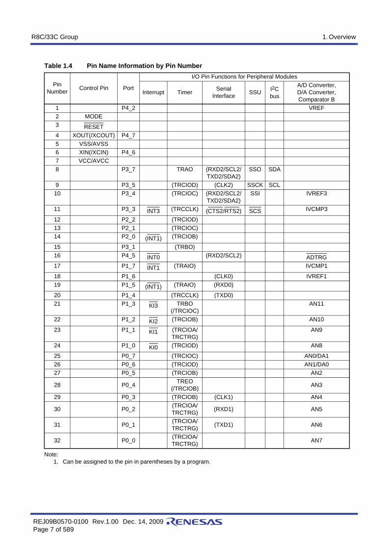
R8C/33C Group 1. Overview
REJ09B0570-0100 Rev.1.00 Dec. 14, 2009Page 7 of 589
Note:1. Can be assigned to the pin in parentheses by a program.
Table 1.4 Pin Name Information by Pin Number
Pin Number Control Pin Port
I/O Pin Functions for Peripheral Modules
Interrupt Timer Serial Interface SSU I2C
bus
A/D Converter,D/A Converter,Comparator B
1 P4_2 VREF2 MODE3 RESET4 XOUT(/XCOUT) P4_75 VSS/AVSS6 XIN(/XCIN) P4_67 VCC/AVCC8 P3_7 TRAO (RXD2/SCL2/
TXD2/SDA2)SSO SDA
9 P3_5 (TRCIOD) (CLK2) SSCK SCL10 P3_4 (TRCIOC) (RXD2/SCL2/
TXD2/SDA2)SSI IVREF3
11 P3_3 INT3 (TRCCLK) (CTS2/RTS2) SCS IVCMP3
12 P2_2 (TRCIOD)13 P2_1 (TRCIOC)14 P2_0 (INT1) (TRCIOB)
15 P3_1 (TRBO)16 P4_5 INT0 (RXD2/SCL2) ADTRG17 P1_7 INT1 (TRAIO) IVCMP1
18 P1_6 (CLK0) IVREF119 P1_5 (INT1) (TRAIO) (RXD0)
20 P1_4 (TRCCLK) (TXD0)21 P1_3 KI3 TRBO
(/TRCIOC)AN11
22 P1_2 KI2 (TRCIOB) AN10
23 P1_1 KI1 (TRCIOA/TRCTRG)
AN9
24 P1_0 KI0 (TRCIOD) AN8
25 P0_7 (TRCIOC) AN0/DA126 P0_6 (TRCIOD) AN1/DA027 P0_5 (TRCIOB) AN2
28 P0_4 TREO(/TRCIOB) AN3
29 P0_3 (TRCIOB) (CLK1) AN4
30 P0_2 (TRCIOA/TRCTRG) (RXD1) AN5
31 P0_1 (TRCIOA/TRCTRG) (TXD1) AN6
32 P0_0 (TRCIOA/TRCTRG) AN7

R8C/33C Group 1. Overview
REJ09B0570-0100 Rev.1.00 Dec. 14, 2009Page 8 of 589
1.5 Pin FunctionsTables 1.5 and 1.6 list Pin Functions.
I: Input O: Output I/O: Input and outputNote:
1. Refer to the oscillator manufacturer for oscillation characteristics.
Table 1.5 Pin Functions (1)
Item Pin Name I/O Type DescriptionPower supply input VCC, VSS − Apply 1.8 V to 5.5 V to the VCC pin. Apply 0 V to the VSS pin.Analog power supply input
AVCC, AVSS − Power supply for the A/D converter.Connect a capacitor between AVCC and AVSS.
Reset input RESET I Input “L” on this pin resets the MCU.MODE MODE I Connect this pin to VCC via a resistor.XIN clock input XIN I These pins are provided for XIN clock generation circuit I/O.
Connect a ceramic resonator or a crystal oscillator betweenthe XIN and XOUT pins (1). To use an external clock, input itto the XOUT pin and leave the XIN pin open.XIN clock output XOUT I/O
XCIN clock input XCIN I These pins are provided for XCIN clock generation circuit I/O.Connect a crystal oscillator between the XCIN and XCOUTpins (1). To use an external clock, input it to the XCIN pin andleave the XCOUT pin open.
XCIN clock output XCOUT O
INT interrupt input INT0, INT1, INT3 I INT interrupt input pins.INT0 is timer RB, and RC input pin.
Key input interrupt KI0 to KI3 I Key input interrupt input pins
Timer RA TRAIO I/O Timer RA I/O pinTRAO O Timer RA output pin
Timer RB TRBO O Timer RB output pinTimer RC TRCCLK I External clock input pin
TRCTRG I External trigger input pinTRCIOA, TRCIOB,TRCIOC, TRCIOD
I/O Timer RC I/O pins
Timer RE TREO O Divided clock output pinSerial interface CLK0, CLK1, CLK2 I/O Transfer clock I/O pins
RXD0, RXD1, RXD2 I Serial data input pinsTXD0, TXD1, TXD2 O Serial data output pins
CTS2 I Transmission control input pin
RTS2 O Reception control output pin
SCL2 I/O I2C mode clock I/O pinSDA2 I/O I2C mode data I/O pin
I2C bus SCL I/O Clock I/O pinSDA I/O Data I/O pin
SSU SSI I/O Data I/O pin
SCS I/O Chip-select signal I/O pin
SSCK I/O Clock I/O pinSSO I/O Data I/O pin

R8C/33C Group 1. Overview
REJ09B0570-0100 Rev.1.00 Dec. 14, 2009Page 9 of 589
I: Input O: Output I/O: Input and output
Table 1.6 Pin Functions (2)
Item Pin Name I/O Type DescriptionReference voltage input
VREF I Reference voltage input pin to A/D converter and D/Aconverter
A/D converter AN0 to AN11 I Analog input pins to A/D converter
ADTRG I A/D external trigger input pin
D/A converter DA0, DA1 O D/A converter output pinsComparator B IVCMP1, IVCMP3 I Comparator B analog voltage input pins
IVREF1, IVREF3 I Comparator B reference voltage input pinsI/O port P0_0 to P0_7,
P1_0 to P1_7, P2_0 to P2_2, P3_1, P3_3 to P3_5, P3_7, P4_5 to P4_7
I/O CMOS I/O ports. Each port has an I/O select directionregister, allowing each pin in the port to be directed for inputor output individually.Any port set to input can be set to use a pull-up resistor or notby a program.All ports can be used as LED drive ports.
Input port P4_2 I Input-only port

R8C/33C Group 2. Central Processing Unit (CPU)
REJ09B0570-0100 Rev.1.00 Dec. 14, 2009Page 10 of 589
2. Central Processing Unit (CPU)Figure 2.1 shows the CPU Registers. The CPU contains 13 registers. R0, R1, R2, R3, A0, A1, and FB configure aregister bank. There are two sets of register bank.
Figure 2.1 CPU Registers
R2b31 b15 b8b7 b0
Data registers (1)
Address registers (1)
R3R0H (high-order of R0)
R2R3A0A1
INTBHb15b19 b0
INTBL
FB Frame base register (1)
The 4 high order bits of INTB are INTBH andthe 16 low order bits of INTB are INTBL.
Interrupt table register
b19 b0
USP
Program counter
ISPSB
User stack pointer
Interrupt stack pointer
Static base register
PC
FLG Flag register
Carry flagDebug flagZero flagSign flagRegister bank select flagOverflow flagInterrupt enable flagStack pointer select flagReserved bitProcessor interrupt priority levelReserved bit
CIPL DZSBOIU
b15 b0
b15 b0
b15 b0b8 b7
Note:1. These registers comprise a register bank. There are two register banks.
R1H (high-order of R1)
R0L (low-order of R0)
R1L (low-order of R1)

R8C/33C Group 2. Central Processing Unit (CPU)
REJ09B0570-0100 Rev.1.00 Dec. 14, 2009Page 11 of 589
2.1 Data Registers (R0, R1, R2, and R3)R0 is a 16-bit register for transfer, arithmetic, and logic operations. The same applies to R1 to R3. R0 can be splitinto high-order bits (R0H) and low-order bits (R0L) to be used separately as 8-bit data registers. R1H and R1L areanalogous to R0H and R0L. R2 can be combined with R0 and used as a 32-bit data register (R2R0). R3R1 isanalogous to R2R0.
2.2 Address Registers (A0 and A1)A0 is a 16-bit register for address register indirect addressing and address register relative addressing. It is alsoused for transfer, arithmetic, and logic operations. A1 is analogous to A0. A1 can be combined with A0 and as a 32-bit address register (A1A0).
2.3 Frame Base Register (FB)FB is a 16-bit register for FB relative addressing.
2.4 Interrupt Table Register (INTB)INTB is a 20-bit register that indicates the starting address of an interrupt vector table.
2.5 Program Counter (PC)PC is 20 bits wide and indicates the address of the next instruction to be executed.
2.6 User Stack Pointer (USP) and Interrupt Stack Pointer (ISP)The stack pointers (SP), USP and ISP, are each 16 bits wide. The U flag of FLG is used to switch betweenUSP and ISP.
2.7 Static Base Register (SB)SB is a 16-bit register for SB relative addressing.
2.8 Flag Register (FLG)FLG is an 11-bit register indicating the CPU state.
2.8.1 Carry Flag (C)The C flag retains carry, borrow, or shift-out bits that have been generated by the arithmetic and logic unit.
2.8.2 Debug Flag (D)The D flag is for debugging only. Set it to 0.
2.8.3 Zero Flag (Z)The Z flag is set to 1 when an arithmetic operation results in 0; otherwise to 0.
2.8.4 Sign Flag (S)The S flag is set to 1 when an arithmetic operation results in a negative value; otherwise to 0.
2.8.5 Register Bank Select Flag (B)Register bank 0 is selected when the B flag is 0. Register bank 1 is selected when this flag is set to 1.
2.8.6 Overflow Flag (O)The O flag is set to 1 when an operation results in an overflow; otherwise to 0.

R8C/33C Group 2. Central Processing Unit (CPU)
REJ09B0570-0100 Rev.1.00 Dec. 14, 2009Page 12 of 589
2.8.7 Interrupt Enable Flag (I)The I flag enables maskable interrupts.Interrupts are disabled when the I flag is set to 0, and are enabled when the I flag is set to 1. The I flag is set to 0when an interrupt request is acknowledged.
2.8.8 Stack Pointer Select Flag (U)ISP is selected when the U flag is set to 0; USP is selected when the U flag is set to 1.The U flag is set to 0 when a hardware interrupt request is acknowledged or the INT instruction of softwareinterrupt numbers 0 to 31 is executed.
2.8.9 Processor Interrupt Priority Level (IPL)IPL is 3 bits wide and assigns processor interrupt priority levels from level 0 to level 7.If a requested interrupt has higher priority than IPL, the interrupt is enabled.
2.8.10 Reserved BitIf necessary, set to 0. When read, the content is undefined.

R8C/33C Group 3. Memory
REJ09B0570-0100 Rev.1.00 Dec. 14, 2009Page 13 of 589
3. Memory
3.1 R8C/33C GroupFigure 3.1 is a Memory Map of R8C/33C Group. The R8C/33C Group has a 1-Mbyte address space from addresses00000h to FFFFFh. The internal ROM (program ROM) is allocated lower addresses, beginning with address0FFFFh. For example, a 32-Kbyte internal ROM area is allocated addresses 08000h to 0FFFFh.The fixed interrupt vector table is allocated addresses 0FFDCh to 0FFFFh. The starting address of each interruptroutine is stored here. The internal ROM (data flash) is allocated addresses 03000h to 03FFFh. The internal RAM is allocated higher addresses, beginning with address 00400h. For example, a 2.5-Kbyte internalRAM area is allocated addresses 00400h to 00DFFh. The internal RAM is used not only for data storage but also asa stack area when a subroutine is called or when an interrupt request is acknowledged.Special function registers (SFRs) are allocated addresses 00000h to 002FFh and 02C00h to 02FFFh. Peripheralfunction control registers are allocated here. All unallocated spaces within the SFRs are reserved and cannot beaccessed by users.
Figure 3.1 Memory Map of R8C/33C Group
0FFFFh
0FFDCh
Notes: 1. Data flash indicates block A (1 Kbyte), block B (1 Kbyte), block C (1 Kbyte), and block D (1 Kbyte). 2. The blank areas are reserved and cannot be accessed by users.
FFFFFh
0FFFFh
0YYYYh
0XXXXh
00400h
002FFh
00000h
Internal ROM(program ROM)
Internal RAM
SFR(Refer to 4. SpecialFunction Registers
(SFRs))
02FFFh
02C00h SFR(Refer to 4. Special Function
Registers (SFRs))
ZZZZZh
Internal ROM(program ROM)
03FFFh
03000hInternal ROM(data flash) (1)
0FFD8h
Reserved area
Undefined instructionOverflow
BRK instructionAddress match
Single stepWatchdog timer, oscillation stop detection, voltage monitor
Address break(Reserved)
Reset
Part Number
R5F21331CNFP, R5F21331CDFPR5F21332CNFP, R5F21332CDFPR5F21334CNFP, R5F21334CDFPR5F21335CNFP, R5F21335CDFPR5F21336CNFP, R5F21336CDFP
Internal ROM Internal RAM
Size Address 0YYYYh Size Address 0XXXXhAddress ZZZZZh
4 Kbytes8 Kbytes
16 Kbytes24 Kbytes32 Kbytes
0F000h0E000h0C000h0A000h08000h
512 bytes1 Kbyte
1.5 Kbytes2 Kbytes
2.5 Kbytes
005FFh007FFh009FFh00BFFh00DFFh
−−−−−

R8C/33C Group 4. Special Function Registers (SFRs)
REJ09B0570-0100 Rev.1.00 Dec. 14, 2009Page 14 of 589
4. Special Function Registers (SFRs)An SFR (special function register) is a control register for a peripheral function. Tables 4.1 to 4.12 list the specialfunction registers and Table 4.13 lists the ID Code Areas and Option Function Select Area.
Table 4.1 SFR Information (1) (1)
X: UndefinedNotes:
1. The blank areas are reserved and cannot be accessed by users.2. The CWR bit in the RSTFR register is set to 0 after power-on and voltage monitor 0 reset. Hardware reset, Software reset, or watchdog timer
reset does not affect this bit.3. The CSPROINI bit in the OFS register is set to 0.4. The LVDAS bit in the OFS register is set to 1.5. The LVDAS bit in the OFS register is set to 0.
Address Register Symbol After Reset0000h0001h0002h0003h0004h Processor Mode Register 0 PM0 00h0005h Processor Mode Register 1 PM1 00h0006h System Clock Control Register 0 CM0 00101000b0007h System Clock Control Register 1 CM1 00100000b0008h Module Standby Control Register MSTCR 00h0009h System Clock Control Register 3 CM3 00h000Ah Protect Register PRCR 00h000Bh Reset Source Determination Register RSTFR 0XXXXXXXb (2)
000Ch Oscillation Stop Detection Register OCD 00000100b000Dh Watchdog Timer Reset Register WDTR XXh000Eh Watchdog Timer Start Register WDTS XXh000Fh Watchdog Timer Control Register WDTC 00111111b0010h0011h0012h0013h0014h0015h High-Speed On-Chip Oscillator Control Register 7 FRA7 When shipping0016h0017h0018h0019h001Ah001Bh001Ch Count Source Protection Mode Register CSPR 00h
10000000b (3)
001Dh001Eh001Fh0020h0021h0022h0023h High-Speed On-Chip Oscillator Control Register 0 FRA0 00h0024h High-Speed On-Chip Oscillator Control Register 1 FRA1 When shipping0025h High-Speed On-Chip Oscillator Control Register 2 FRA2 00h0026h On-Chip Reference Voltage Control Register OCVREFCR 00h0027h0028h Clock Prescaler Reset Flag CPSRF 00h0029h High-Speed On-Chip Oscillator Control Register 4 FRA4 When Shipping002Ah High-Speed On-Chip Oscillator Control Register 5 FRA5 When Shipping002Bh High-Speed On-Chip Oscillator Control Register 6 FRA6 When Shipping002Ch002Dh002Eh002Fh High-Speed On-Chip Oscillator Control Register 3 FRA3 When shipping0030h Voltage Monitor Circuit Control Register CMPA 00h0031h Voltage Monitor Circuit Edge Select Register VCAC 00h0032h0033h Voltage Detect Register 1 VCA1 00001000b0034h Voltage Detect Register 2 VCA2 00h (4)
00100000b (5)
0035h0036h Voltage Detection 1 Level Select Register VD1LS 00000111b0037h0038h Voltage Monitor 0 Circuit Control Register VW0C 1100X010b (4)
1100X011b (5)
0039h Voltage Monitor 1 Circuit Control Register VW1C 10001010b

R8C/33C Group 4. Special Function Registers (SFRs)
REJ09B0570-0100 Rev.1.00 Dec. 14, 2009Page 15 of 589
Table 4.2 SFR Information (2) (1)
X: UndefinedNotes:
1. The blank areas are reserved and cannot be accessed by users.2. Selectable by the IICSEL bit in the SSUIICSR register.
Address Register Symbol After Reset003Ah Voltage Monitor 2 Circuit Control Register VW2C 10000010b003Bh003Ch003Dh003Eh003Fh0040h0041h Flash Memory Ready Interrupt Control Register FMRDYIC XXXXX000b0042h0043h0044h0045h0046h0047h Timer RC Interrupt Control Register TRCIC XXXXX000b0048h0049h004Ah Timer RE Interrupt Control Register TREIC XXXXX000b004Bh UART2 Transmit Interrupt Control Register S2TIC XXXXX000b004Ch UART2 Receive Interrupt Control Register S2RIC XXXXX000b004Dh Key Input Interrupt Control Register KUPIC XXXXX000b004Eh A/D Conversion Interrupt Control Register ADIC XXXXX000b004Fh SSU Interrupt Control Register / IIC bus Interrupt Control Register (2) SSUIC / IICIC XXXXX000b0050h0051h UART0 Transmit Interrupt Control Register S0TIC XXXXX000b0052h UART0 Receive Interrupt Control Register S0RIC XXXXX000b0053h UART1 Transmit Interrupt Control Register S1TIC XXXXX000b0054h UART1 Receive Interrupt Control Register S1RIC XXXXX000b0055h0056h Timer RA Interrupt Control Register TRAIC XXXXX000b0057h0058h Timer RB Interrupt Control Register TRBIC XXXXX000b0059h INT1 Interrupt Control Register INT1IC XX00X000b005Ah INT3 Interrupt Control Register INT3IC XX00X000b005Bh005Ch005Dh INT0 Interrupt Control Register INT0IC XX00X000b005Eh UART2 Bus Collision Detection Interrupt Control Register U2BCNIC XXXXX000b005Fh0060h0061h0062h0063h0064h0065h0066h0067h0068h0069h006Ah006Bh006Ch006Dh006Eh006Fh0070h0071h0072h Voltage Monitor 1 Interrupt Control Register VCMP1IC XXXXX000b0073h Voltage Monitor 2 Interrupt Control Register VCMP2IC XXXXX000b0074h0075h0076h0077h0078h0079h007Ah007Bh007Ch007Dh007Eh007Fh
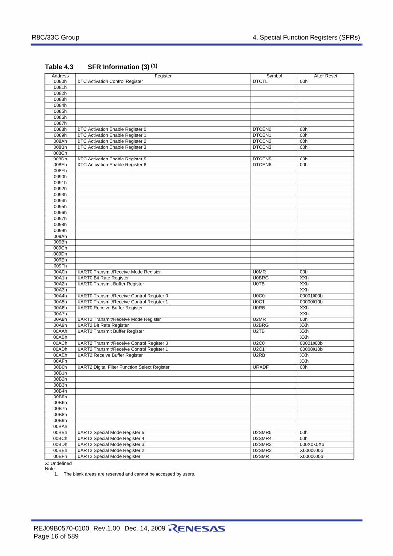
R8C/33C Group 4. Special Function Registers (SFRs)
REJ09B0570-0100 Rev.1.00 Dec. 14, 2009Page 16 of 589
Table 4.3 SFR Information (3) (1)
X: UndefinedNote:
1. The blank areas are reserved and cannot be accessed by users.
Address Register Symbol After Reset0080h DTC Activation Control Register DTCTL 00h0081h0082h0083h0084h0085h0086h0087h0088h DTC Activation Enable Register 0 DTCEN0 00h0089h DTC Activation Enable Register 1 DTCEN1 00h008Ah DTC Activation Enable Register 2 DTCEN2 00h008Bh DTC Activation Enable Register 3 DTCEN3 00h008Ch008Dh DTC Activation Enable Register 5 DTCEN5 00h008Eh DTC Activation Enable Register 6 DTCEN6 00h008Fh0090h0091h0092h0093h0094h0095h0096h0097h0098h0099h009Ah009Bh009Ch009Dh009Eh009Fh00A0h UART0 Transmit/Receive Mode Register U0MR 00h00A1h UART0 Bit Rate Register U0BRG XXh00A2h UART0 Transmit Buffer Register U0TB XXh00A3h XXh00A4h UART0 Transmit/Receive Control Register 0 U0C0 00001000b00A5h UART0 Transmit/Receive Control Register 1 U0C1 00000010b00A6h UART0 Receive Buffer Register U0RB XXh00A7h XXh00A8h UART2 Transmit/Receive Mode Register U2MR 00h00A9h UART2 Bit Rate Register U2BRG XXh00AAh UART2 Transmit Buffer Register U2TB XXh00ABh XXh00ACh UART2 Transmit/Receive Control Register 0 U2C0 00001000b00ADh UART2 Transmit/Receive Control Register 1 U2C1 00000010b00AEh UART2 Receive Buffer Register U2RB XXh00AFh XXh00B0h UART2 Digital Filter Function Select Register URXDF 00h00B1h00B2h00B3h00B4h00B5h00B6h00B7h00B8h00B9h00BAh00BBh UART2 Special Mode Register 5 U2SMR5 00h00BCh UART2 Special Mode Register 4 U2SMR4 00h00BDh UART2 Special Mode Register 3 U2SMR3 000X0X0Xb00BEh UART2 Special Mode Register 2 U2SMR2 X0000000b00BFh UART2 Special Mode Register U2SMR X0000000b

R8C/33C Group 4. Special Function Registers (SFRs)
REJ09B0570-0100 Rev.1.00 Dec. 14, 2009Page 17 of 589
Table 4.4 SFR Information (4) (1)
X: UndefinedNote:
1. The blank areas are reserved and cannot be accessed by users.
Address Register Symbol After Reset00C0h A/D Register 0 AD0 XXXh
000000XXb00C1h00C2h A/D Register 1 AD1 XXh00C3h 000000XXb00C4h A/D Register 2 AD2 XXh00C5h 000000XXb00C6h A/D Register 3 AD3 XXh00C7h 000000XXb00C8h A/D Register 4 AD4 XXh00C9h 000000XXb00CAh A/D Register 5 AD5 XXh00CBh 000000XXb00CCh A/D Register 6 AD6 XXh00CDh 000000XXb00CEh A/D Register 7 AD7 XXh00CFh 000000XXb00D0h00D1h00D2h00D3h00D4h A/D Mode Register ADMOD 00h00D5h A/D Input Select Register ADINSEL 11000000b00D6h A/D Control Register 0 ADCON0 00h00D7h A/D Control Register 1 ADCON1 00h00D8h D/A0 Register DA0 00h00D9h D/A1 Register DA1 00h00DAh00DBh00DCh D/A Control Register DACON 00h00DDh00DEh00DFh00E0h Port P0 Register P0 XXh00E1h Port P1 Register P1 XXh00E2h Port P0 Direction Register PD0 00h00E3h Port P1 Direction Register PD1 00h00E4h Port P2 Register P2 XXh00E5h Port P3 Register P3 XXh00E6h Port P2 Direction Register PD2 00h00E7h Port P3 Direction Register PD3 00h00E8h Port P4 Register P4 XXh00E9h00EAh Port P4 Direction Register PD4 00h00EBh00ECh00EDh00EEh00EFh00F0h00F1h00F2h00F3h00F4h00F5h00F6h00F7h00F8h00F9h00FAh00FBh00FCh00FDh00FEh00FFh

R8C/33C Group 4. Special Function Registers (SFRs)
REJ09B0570-0100 Rev.1.00 Dec. 14, 2009Page 18 of 589
Table 4.5 SFR Information (5) (1)
Note:1. The blank areas are reserved and cannot be accessed by users.
Address Register Symbol After Reset0100h Timer RA Control Register TRACR 00h0101h Timer RA I/O Control Register TRAIOC 00h0102h Timer RA Mode Register TRAMR 00h0103h Timer RA Prescaler Register TRAPRE FFh0104h Timer RA Register TRA FFh0105h LIN Control Register 2 LINCR2 00h0106h LIN Control Register LINCR 00h0107h LIN Status Register LINST 00h0108h Timer RB Control Register TRBCR 00h0109h Timer RB One-Shot Control Register TRBOCR 00h010Ah Timer RB I/O Control Register TRBIOC 00h010Bh Timer RB Mode Register TRBMR 00h010Ch Timer RB Prescaler Register TRBPRE FFh010Dh Timer RB Secondary Register TRBSC FFh010Eh Timer RB Primary Register TRBPR FFh010Fh0110h0111h0112h0113h0114h0115h0116h0117h0118h Timer RE Second Data Register / Counter Data Register TRESEC 00h0119h Timer RE Minute Data Register / Compare Data Register TREMIN 00h011Ah Timer RE Hour Data Register TREHR 00h011Bh Timer RE Day of Week Data Register TREWK 00h011Ch Timer RE Control Register 1 TRECR1 00h011Dh Timer RE Control Register 2 TRECR2 00h011Eh Timer RE Count Source Select Register TRECSR 00001000b011Fh0120h Timer RC Mode Register TRCMR 01001000b0121h Timer RC Control Register 1 TRCCR1 00h0122h Timer RC Interrupt Enable Register TRCIER 01110000b0123h Timer RC Status Register TRCSR 01110000b0124h Timer RC I/O Control Register 0 TRCIOR0 10001000b0125h Timer RC I/O Control Register 1 TRCIOR1 10001000b0126h Timer RC Counter TRC 00h0127h 00h0128h Timer RC General Register A TRCGRA FFh0129h FFh012Ah Timer RC General Register B TRCGRB FFh012Bh FFh012Ch Timer RC General Register C TRCGRC FFh012Dh FFh012Eh Timer RC General Register D TRCGRD FFh012Fh FFh0130h Timer RC Control Register 2 TRCCR2 00011000b0131h Timer RC Digital Filter Function Select Register TRCDF 00h0132h Timer RC Output Master Enable Register TRCOER 01111111b0133h Timer RC Trigger Control Register TRCADCR 00h0134h0135h0136h0137h0138h0139h013Ah013Bh013Ch013Dh013Eh013Fh

R8C/33C Group 4. Special Function Registers (SFRs)
REJ09B0570-0100 Rev.1.00 Dec. 14, 2009Page 19 of 589
Table 4.6 SFR Information (6) (1)
X: UndefinedNote:
1. The blank areas are reserved and cannot be accessed by users.
Address Register Symbol After Reset0140h0141h0142h0143h0144h0145h0146h0147h0148h0149h014Ah014Bh014Ch014Dh014Eh014Fh0150h0151h0152h0153h0154h0155h0156h0157h0158h0159h015Ah015Bh015Ch015Dh015Eh015Fh0160h UART1 Transmit/Receive Mode Register U1MR 00h0161h UART1 Bit Rate Register U1BRG XXh0162h UART1 Transmit Buffer Register U1TB XXh0163h XXh0164h UART1 Transmit/Receive Control Register 0 U1C0 00001000b0165h UART1 Transmit/Receive Control Register 1 U1C1 00000010b0166h UART1 Receive Buffer Register U1RB XXh0167h XXh0168h0169h016Ah016Bh016Ch016Dh016Eh016Fh0170h0171h0172h0173h0174h0175h0176h0177h0178h0179h017Ah017Bh017Ch017Dh017Eh017Fh

R8C/33C Group 4. Special Function Registers (SFRs)
REJ09B0570-0100 Rev.1.00 Dec. 14, 2009Page 20 of 589
Table 4.7 SFR Information (7) (1)
X: UndefinedNotes:
1. The blank areas are reserved and cannot be accessed by users.2. Selectable by the IICSEL bit in the SSUIICSR register.
Address Register Symbol After Reset0180h Timer RA Pin Select Register TRASR 00h0181h Timer RB/RC Pin Select Register TRBRCSR 00h0182h Timer RC Pin Select Register 0 TRCPSR0 00h0183h Timer RC Pin Select Register 1 TRCPSR1 00h0184h0185h0186h0187h0188h UART0 Pin Select Register U0SR 00h0189h UART1 Pin Select Register U1SR 00h018Ah UART2 Pin Select Register 0 U2SR0 00h018Bh UART2 Pin Select Register 1 U2SR1 00h018Ch SSU/IIC Pin Select Register SSUIICSR 00h018Dh018Eh INT Interrupt Input Pin Select Register INTSR 00h018Fh I/O Function Pin Select Register PINSR 00h0190h0191h0192h0193h SS Bit Counter Register SSBR 11111000b0194h SS Transmit Data Register L / IIC bus Transmit Data Register (2) SSTDR / ICDRT FFh0195h SS Transmit Data Register H (2) SSTDRH FFh0196h SS Receive Data Register L / IIC bus Receive Data Register (2) SSRDR / ICDRR FFh0197h SS Receive Data Register H (2) SSRDRH FFh0198h SS Control Register H / IIC bus Control Register 1 (2) SSCRH / ICCR1 00h0199h SS Control Register L / IIC bus Control Register 2 (2) SSCRL / ICCR2 01111101b019Ah SS Mode Register / IIC bus Mode Register (2) SSMR / ICMR 00010000b / 00011000b019Bh SS Enable Register / IIC bus Interrupt Enable Register (2) SSER / ICIER 00h019Ch SS Status Register / IIC bus Status Register (2) SSSR / ICSR 00h / 0000X000b019Dh SS Mode Register 2 / Slave Address Register (2) SSMR2 / SAR 00h019Eh019Fh01A0h01A1h01A2h01A3h01A4h01A5h01A6h01A7h01A8h01A9h01AAh01ABh01ACh01ADh01AEh01AFh01B0h01B1h01B2h Flash Memory Status Register FST 10000X00b01B3h01B4h Flash Memory Control Register 0 FMR0 00h01B5h Flash Memory Control Register 1 FMR1 00h01B6h Flash Memory Control Register 2 FMR2 00h01B7h01B8h01B9h01BAh01BBh01BCh01BDh01BEh01BFh

R8C/33C Group 4. Special Function Registers (SFRs)
REJ09B0570-0100 Rev.1.00 Dec. 14, 2009Page 21 of 589
Table 4.8 SFR Information (8) (1)
X: UndefinedNote:
1. The blank areas are reserved and cannot be accessed by users.
Address Register Symbol After Reset01C0h Address Match Interrupt Register 0 RMAD0 XXh01C1h XXh01C2h 0000XXXXb01C3h Address Match Interrupt Enable Register 0 AIER0 00h01C4h Address Match Interrupt Register 1 RMAD1 XXh01C5h XXh01C6h 0000XXXXb01C7h Address Match Interrupt Enable Register 1 AIER1 00h01C8h01C9h01CAh01CBh01CCh01CDh01CEh01CFh01D0h01D1h01D2h01D3h01D4h01D5h01D6h01D7h01D8h01D9h01DAh01DBh01DCh01DDh01DEh01DFh01E0h Pull-Up Control Register 0 PUR0 00h01E1h Pull-Up Control Register 1 PUR1 00h01E2h01E3h01E4h01E5h01E6h01E7h01E8h01E9h01EAh01EBh01ECh01EDh01EEh01EFh01F0h Port P1 Drive Capacity Control Register P1DRR 00h01F1h Port P2 Drive Capacity Control Register P2DRR 00h01F2h Drive Capacity Control Register 0 DRR0 00h01F3h Drive Capacity Control Register 1 DRR1 00h01F4h01F5h Input Threshold Control Register 0 VLT0 00h01F6h Input Threshold Control Register 1 VLT1 00h01F7h01F8h Comparator B Control Register 0 INTCMP 00h01F9h01FAh External Input Enable Register 0 INTEN 00h01FBh01FCh INT Input Filter Select Register 0 INTF 00h01FDh01FEh Key Input Enable Register 0 KIEN 00h01FFh

R8C/33C Group 4. Special Function Registers (SFRs)
REJ09B0570-0100 Rev.1.00 Dec. 14, 2009Page 22 of 589
Table 4.9 SFR Information (9) (1)
X: UndefinedNote:
1. The blank areas are reserved and cannot be accessed by users.
Address Register Symbol After Reset2C00h DTC Transfer Vector Area XXh2C01h DTC Transfer Vector Area XXh2C02h DTC Transfer Vector Area XXh2C03h DTC Transfer Vector Area XXh2C04h DTC Transfer Vector Area XXh2C05h DTC Transfer Vector Area XXh2C06h DTC Transfer Vector Area XXh2C07h DTC Transfer Vector Area XXh2C08h DTC Transfer Vector Area XXh2C09h DTC Transfer Vector Area XXh2C0Ah DTC Transfer Vector Area XXh
: DTC Transfer Vector Area XXh: DTC Transfer Vector Area XXh
2C3Ah DTC Transfer Vector Area XXh2C3Bh DTC Transfer Vector Area XXh2C3Ch DTC Transfer Vector Area XXh2C3Dh DTC Transfer Vector Area XXh2C3Eh DTC Transfer Vector Area XXh2C3Fh DTC Transfer Vector Area XXh2C40h DTC Control Data 0 DTCD0 XXh2C41h XXh2C42h XXh2C43h XXh2C44h XXh2C45h XXh2C46h XXh2C47h XXh2C48h DTC Control Data 1 DTCD1 XXh2C49h XXh2C4Ah XXh2C4Bh XXh2C4Ch XXh2C4Dh XXh2C4Eh XXh2C4Fh XXh2C50h DTC Control Data 2 DTCD2 XXh2C51h XXh2C52h XXh2C53h XXh2C54h XXh2C55h XXh2C56h XXh2C57h XXh2C58h DTC Control Data 3 DTCD3 XXh2C59h XXh2C5Ah XXh2C5Bh XXh2C5Ch XXh2C5Dh XXh2C5Eh XXh2C5Fh XXh2C60h DTC Control Data 4 DTCD4 XXh2C61h XXh2C62h XXh2C63h XXh2C64h XXh2C65h XXh2C66h XXh2C67h XXh2C68h DTC Control Data 5 DTCD5 XXh2C69h XXh2C6Ah XXh2C6Bh XXh2C6Ch XXh2C6Dh XXh2C6Eh XXh2C6Fh XXh

R8C/33C Group 4. Special Function Registers (SFRs)
REJ09B0570-0100 Rev.1.00 Dec. 14, 2009Page 23 of 589
Table 4.10 SFR Information (10) (1)
X: UndefinedNote:
1. The blank areas are reserved and cannot be accessed by users.
Address Register Symbol After Reset2C70h DTC Control Data 6 DTCD6 XXh2C71h XXh2C72h XXh2C73h XXh2C74h XXh2C75h XXh2C76h XXh2C77h XXh2C78h DTC Control Data 7 DTCD7 XXh2C79h XXh2C7Ah XXh2C7Bh XXh2C7Ch XXh2C7Dh XXh2C7Eh XXh2C7Fh XXh2C80h DTC Control Data 8 DTCD8 XXh2C81h XXh2C82h XXh2C83h XXh2C84h XXh2C85h XXh2C86h XXh2C87h XXh2C88h DTC Control Data 9 DTCD9 XXh2C89h XXh2C8Ah XXh2C8Bh XXh2C8Ch XXh2C8Dh XXh2C8Eh XXh2C8Fh XXh2C90h DTC Control Data 10 DTCD10 XXh2C91h XXh2C92h XXh2C93h XXh2C94h XXh2C95h XXh2C96h XXh2C97h XXh2C98h DTC Control Data 11 DTCD11 XXh2C99h XXh2C9Ah XXh2C9Bh XXh2C9Ch XXh2C9Dh XXh2C9Eh XXh2C9Fh XXh2CA0h DTC Control Data 12 DTCD12 XXh2CA1h XXh2CA2h XXh2CA3h XXh2CA4h XXh2CA5h XXh2CA6h XXh2CA7h XXh2CA8h DTC Control Data 13 DTCD13 XXh2CA9h XXh2CAAh XXh2CABh XXh2CACh XXh2CADh XXh2CAEh XXh2CAFh XXh

R8C/33C Group 4. Special Function Registers (SFRs)
REJ09B0570-0100 Rev.1.00 Dec. 14, 2009Page 24 of 589
Table 4.11 SFR Information (11) (1)
X: UndefinedNote:
1. The blank areas are reserved and cannot be accessed by users.
Address Register Symbol After Reset2CB0h DTC Control Data 14 DTCD14 XXh2CB1h XXh2CB2h XXh2CB3h XXh2CB4h XXh2CB5h XXh2CB6h XXh2CB7h XXh2CB8h DTC Control Data 15 DTCD15 XXh2CB9h XXh2CBAh XXh2CBBh XXh2CBCh XXh2CBDh XXh2CBEh XXh2CBFh XXh2CC0h DTC Control Data 16 DTCD16 XXh2CC1h XXh2CC2h XXh2CC3h XXh2CC4h XXh2CC5h XXh2CC6h XXh2CC7h XXh2CC8h DTC Control Data 17 DTCD17 XXh2CC9h XXh2CCAh XXh2CCBh XXh2CCCh XXh2CCDh XXh2CCEh XXh2CCFh XXh2CD0h DTC Control Data 18 DTCD18 XXh2CD1h XXh2CD2h XXh2CD3h XXh2CD4h XXh2CD5h XXh2CD6h XXh2CD7h XXh2CD8h DTC Control Data 19 DTCD19 XXh2CD9h XXh2CDAh XXh2CDBh XXh2CDCh XXh2CDDh XXh2CDEh XXh2CDFh XXh2CE0h DTC Control Data 20 DTCD20 XXh2CE1h XXh2CE2h XXh2CE3h XXh2CE4h XXh2CE5h XXh2CE6h XXh2CE7h XXh2CE8h DTC Control Data 21 DTCD21 XXh2CE9h XXh2CEAh XXh2CEBh XXh2CECh XXh2CEDh XXh2CEEh XXh2CEFh XXh

R8C/33C Group 4. Special Function Registers (SFRs)
REJ09B0570-0100 Rev.1.00 Dec. 14, 2009Page 25 of 589
Table 4.12 SFR Information (12) (1)
X: UndefinedNote:
1. The blank areas are reserved and cannot be accessed by users.
Table 4.13 ID Code Areas and Option Function Select Area
Notes:1. The option function select area is allocated in the flash memory, not in the SFRs. Set appropriate values as ROM data by a program.
Do not write additions to the option function select area. If the block including the option function select area is erased, the option function select area is set to FFh.When blank products are shipped, the option function select area is set to FFh. It is set to the written value after written by the user.When factory-programming products are shipped, the value of the option function select area is the value programmed by the user.
2. The ID code areas are allocated in the flash memory, not in the SFRs. Set appropriate values as ROM data by a program.Do not write additions to the ID code areas. If the block including the ID code areas is erased, the ID code areas are set to FFh.When blank products are shipped, the ID code areas are set to FFh. They are set to the written value after written by the user.When factory-programming products are shipped, the value of the ID code areas is the value programmed by the user.
Address Register Symbol After Reset2CF0h DTC Control Data 22 DTCD22 XXh2CF1h XXh2CF2h XXh2CF3h XXh2CF4h XXh2CF5h XXh2CF6h XXh2CF7h XXh2CF8h DTC Control Data 23 DTCD23 XXh2CF9h XXh2CFAh XXh2CFBh XXh2CFCh XXh2CFDh XXh2CFEh XXh2CFFh XXh2D00h
:2FFFh
Address Area Name Symbol After Reset:
FFDBh Option Function Select Register 2 OFS2 (Note 1):
FFDFh ID1 (Note 2):
FFE3h ID2 (Note 2):
FFEBh ID3 (Note 2):
FFEFh ID4 (Note 2):
FFF3h ID5 (Note 2):
FFF7h ID6 (Note 2):
FFFBh ID7 (Note 2):
FFFFh Option Function Select Register OFS (Note 1)

R8C/33C Group 5. Resets
REJ09B0570-0100 Rev.1.00 Dec. 14, 2009Page 26 of 589
5. ResetsThe following resets are implemented: hardware reset, power-on reset, voltage monitor 0 reset, watchdog timer reset,and software reset.Table 5.1 lists the Reset Names and Sources. Figure 5.1 shows the Block Diagram of Reset Circuit.
Figure 5.1 Block Diagram of Reset Circuit
Table 5.1 Reset Names and Sources Reset Name Source
Hardware reset Input voltage of RESET pin is held “L”Power-on reset VCC risesVoltage monitor 0 reset VCC falls (monitor voltage: Vdet0)Watchdog timer reset Underflow of watchdog timerSoftware reset Write 1 to PM03 bit in PM0 register
RESET
Power-on resetcircuit
Voltagedetection
circuit
Watchdogtimer
CPU
Pin, CPU, and SFR (1)
VCC
Hardware reset
Power-on reset
Voltage monitor 0 reset
Watchdog timerreset
Software reset
Note:1. The CWR bit in the RSTFR register is set to 0 (cold start-up) after power-on or
voltage monitor 0 reset. This bit remains unchanged at a hardware reset,software reset, or watchdog timer reset.

R8C/33C Group 5. Resets
REJ09B0570-0100 Rev.1.00 Dec. 14, 2009Page 27 of 589
Table 5.2 lists the Pin Functions while RESET Pin Level is “L”, Figure 5.2 shows the CPU Register Status after Reset,Figure 5.3 shows the Reset Sequence.
Figure 5.2 CPU Register Status after Reset
Figure 5.3 Reset Sequence
Table 5.2 Pin Functions while RESET Pin Level is “L”Pin Name Pin Function
P0, P1, P2_0 to P2_2, P3_1, P3_3 to P3_5, P3_7
Input port
P4_2, P4_5 to P4_7 Input port
b19 b0
Interrupt table register (INTB)Program counter (PC)
User stack pointer (USP)
Interrupt stack pointer (ISP)
Static base register (SB)
Content of addresses 0FFFEh to 0FFFCh
Flag register (FLG)
CIPL DZSBOIU
b15 b0
b15 b0
b15 b0b8 b7
b15 b0
0000h0000h0000h0000h0000h0000h0000h
Data register (R0)
Data register (R1)
Data register (R2)
Data register (R3)
Address register (A0)
Address register (A1)
Frame base register (FB)
00000h
0000h0000h0000h
0000h
Start time of flash memory(CPU clock × 148 cycles)
0FFFCh 0FFFEh
0FFFDh Content of reset vector
CPU clock
Address(internal addresssignal)
Notes:1. Hardware reset.2. When the “L” input width to the RESET pin is set to fOCO-S clock × 32 cycles or more, setting the RESET pin to “H” also sets the internal
reset signal to “H” at the same time.
CPU clock × 28 cycles
fOCO-S clock × 32 cycles (2)
fOCO-S
Internal resetsignal
RESET pin
10 µs or more are needed (1)

R8C/33C Group 5. Resets
REJ09B0570-0100 Rev.1.00 Dec. 14, 2009Page 28 of 589
5.1 Registers
5.1.1 Processor Mode Register 0 (PM0)
Set the PRC1 bit in the PRCR register to 1 (write enabled) before rewriting the PM0 register.
5.1.2 Reset Source Determination Register (RSTFR)
Notes:1. The CWR bit is set to 0 (cold start-up) after power-on or voltage monitor 0 reset. This bit remains unchanged at a
hardware reset, software reset, or watchdog timer reset.2. If 1 is written to the CWR bit by a program, it is set to 1. (Writing 0 does not affect this bit.)3. When the VW0C0 bit in the VW0C register is set to 0 (voltage monitor 0 reset disabled), the CWR bit value is
undefined.
Address 0004hBit b7 b6 b5 b4 b3 b2 b1 b0
Symbol — — — — PM03 — — —After Reset 0 0 0 0 0 0 0 0
Bit Symbol Bit Name Function R/Wb0 — Reserved bits Set to 0. R/Wb1 —b2 —b3 PM03 Software reset bit The MCU is reset when this bit is set to 1. When
read, the content is 0.R/W
b4 — Nothing is assigned. If necessary, set to 0. When read, the content is 0. —b5 —b6 —b7 —
Address 000BhBit b7 b6 b5 b4 b3 b2 b1 b0
Symbol — — — — WDR SWR HWR CWRAfter Reset 0 X X X X X X X (Note 1)
Bit Symbol Bit Name Function R/Wb0 CWR Cold start-up/warm start-up
determine flag (2, 3)0: Cold start-up1: Warm start-up
R/W
b1 HWR Hardware reset detect flag 0: Not detected1: Detected
R
b2 SWR Software reset detect flag 0: Not detected1: Detected
R
b3 WDR Watchdog timer reset detect flag 0: Not detected1: Detected
R
b4 — Reserved bits When read, the content is undefined. Rb5 —b6 —b7 — Reserved bit Set to 0. R/W
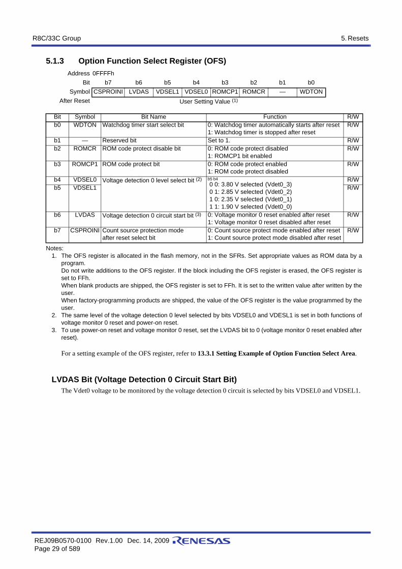
R8C/33C Group 5. Resets
REJ09B0570-0100 Rev.1.00 Dec. 14, 2009Page 29 of 589
5.1.3 Option Function Select Register (OFS)
Notes:1. The OFS register is allocated in the flash memory, not in the SFRs. Set appropriate values as ROM data by a
program.Do not write additions to the OFS register. If the block including the OFS register is erased, the OFS register isset to FFh.When blank products are shipped, the OFS register is set to FFh. It is set to the written value after written by theuser.When factory-programming products are shipped, the value of the OFS register is the value programmed by theuser.
2. The same level of the voltage detection 0 level selected by bits VDSEL0 and VDESL1 is set in both functions ofvoltage monitor 0 reset and power-on reset.
3. To use power-on reset and voltage monitor 0 reset, set the LVDAS bit to 0 (voltage monitor 0 reset enabled afterreset).
For a setting example of the OFS register, refer to 13.3.1 Setting Example of Option Function Select Area.
LVDAS Bit (Voltage Detection 0 Circuit Start Bit)The Vdet0 voltage to be monitored by the voltage detection 0 circuit is selected by bits VDSEL0 and VDSEL1.
Address 0FFFFhBit b7 b6 b5 b4 b3 b2 b1 b0
Symbol CSPROINI LVDAS VDSEL1 VDSEL0 ROMCP1 ROMCR — WDTONAfter Reset User Setting Value (1)
Bit Symbol Bit Name Function R/Wb0 WDTON Watchdog timer start select bit 0: Watchdog timer automatically starts after reset
1: Watchdog timer is stopped after resetR/W
b1 — Reserved bit Set to 1. R/Wb2 ROMCR ROM code protect disable bit 0: ROM code protect disabled
1: ROMCP1 bit enabledR/W
b3 ROMCP1 ROM code protect bit 0: ROM code protect enabled1: ROM code protect disabled
R/W
b4 VDSEL0 Voltage detection 0 level select bit (2) b5 b4 0 0: 3.80 V selected (Vdet0_3) 0 1: 2.85 V selected (Vdet0_2) 1 0: 2.35 V selected (Vdet0_1) 1 1: 1.90 V selected (Vdet0_0)
R/Wb5 VDSEL1 R/W
b6 LVDAS Voltage detection 0 circuit start bit (3) 0: Voltage monitor 0 reset enabled after reset1: Voltage monitor 0 reset disabled after reset
R/W
b7 CSPROINI Count source protection mode after reset select bit
0: Count source protect mode enabled after reset1: Count source protect mode disabled after reset
R/W

R8C/33C Group 5. Resets
REJ09B0570-0100 Rev.1.00 Dec. 14, 2009Page 30 of 589
5.1.4 Option Function Select Register 2 (OFS2)
Note:1. The OFS2 register is allocated in the flash memory, not in the SFRs. Set appropriate values as ROM data by a
program.Do not write additions to the OFS2 register. If the block including the OFS2 register is erased, the OFS2 registeris set to FFh.When blank products are shipped, the OFS2 register is set to FFh. It is set to the written value after written by theuser.When factory-programming products are shipped, the value of the OFS2 register is the value programmed by theuser.
For a setting example of the OFS2 register, refer to 13.3.1 Setting Example of Option Function Select Area.
Bits WDTRCS0 and WDTRCS1 (Watchdog Timer Refresh Acknowledgement Period Set Bit)
Assuming that the period from when the watchdog timer starts counting until it underflows is 100%, the refreshacknowledgement period for the watchdog timer can be selected. For details, refer to 14.3.1.1 Refresh Acknowledgement Period.
Address 0FFDBhBit b7 b6 b5 b4 b3 b2 b1 b0
Symbol — — — — WDTRCS1 WDTRCS0 WDTUFS1 WDTUFS0After Reset User Setting Value (1)
Bit Symbol Bit Name Function R/Wb0 WDTUFS0 Watchdog timer underflow period set bit b1 b0
0 0: 03FFh 0 1: 0FFFh 1 0: 1FFFh 1 1: 3FFFh
R/Wb1 WDTUFS1 R/W
b2 WDTRCS0 Watchdog timer refresh acknowledgement period set bit
b3 b2 0 0: 25% 0 1: 50% 1 0: 75% 1 1: 100%
R/Wb3 WDTRCS1 R/W
b4 — Reserved bits Set to 1. R/Wb5 —b6 —b7 —

R8C/33C Group 5. Resets
REJ09B0570-0100 Rev.1.00 Dec. 14, 2009Page 31 of 589
5.2 Hardware ResetA reset is applied using the RESET pin. When an “L” signal is applied to the RESET pin while the supply voltagemeets the recommended operating conditions, pins, CPU, and SFRs are all reset (refer to Table 5.2 Pin Functionswhile RESET Pin Level is “L”, Figure 5.2 CPU Register Status after Reset, and Table 4.1 to Table 4.12 SFRInformation). When the input level applied to the RESET pin changes from “L” to “H”, a program is executed beginning with theaddress indicated by the reset vector. After reset, the low-speed on-chip oscillator clock with no division isautomatically selected as the CPU clock.Refer to 4. Special Function Registers (SFRs) for the states of the SFRs after reset.The internal RAM is not reset. If the RESET pin is pulled “L” while writing to the internal RAM is in progress, thecontents of internal RAM will be undefined.Figure 5.4 shows an Example of Hardware Reset Circuit and Operation and Figure 5.5 shows an Example ofHardware Reset Circuit (Usage Example of External Supply Voltage Detection Circuit) and Operation.
5.2.1 When Power Supply is Stable(1) Apply “L” to the RESET pin.(2) Wait for 10 µs.(3) Apply “H” to the RESET pin.
5.2.2 Power On(1) Apply “L” to the RESET pin.(2) Let the supply voltage increase until it meets the recommended operating conditions.(3) Wait for td(P-R) or more to allow the internal power supply to stabilize (refer to 32. Electrical
Characteristics).(4) Wait for 10 µs.(5) Apply “H” to the RESET pin.

R8C/33C Group 5. Resets
REJ09B0570-0100 Rev.1.00 Dec. 14, 2009Page 32 of 589
Figure 5.4 Example of Hardware Reset Circuit and Operation
Figure 5.5 Example of Hardware Reset Circuit (Usage Example of External Supply Voltage Detection Circuit) and Operation
RESET
VCCVCC
RESET
1.8 V
0 V0.2 VCC or below
td(P-R) + 10 µs or more
0 V
Note:
1. Refer to 32. Electrical Characteristics.
RESET VCCVCC
RESET
1.8 V
0 V
0 V
5 V
5 V
Example whenVCC = 5 V
Supply voltagedetection circuit
Note:
1. Refer to 32. Electrical Characteristics.
td(P-R) + 10 µs or more
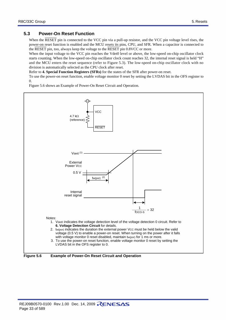
R8C/33C Group 5. Resets
REJ09B0570-0100 Rev.1.00 Dec. 14, 2009Page 33 of 589
5.3 Power-On Reset FunctionWhen the RESET pin is connected to the VCC pin via a pull-up resistor, and the VCC pin voltage level rises, thepower-on reset function is enabled and the MCU resets its pins, CPU, and SFR. When a capacitor is connected tothe RESET pin, too, always keep the voltage to the RESET pin 0.8VCC or more.When the input voltage to the VCC pin reaches the Vdet0 level or above, the low-speed on-chip oscillator clockstarts counting. When the low-speed on-chip oscillator clock count reaches 32, the internal reset signal is held “H”and the MCU enters the reset sequence (refer to Figure 5.3). The low-speed on-chip oscillator clock with nodivision is automatically selected as the CPU clock after reset.Refer to 4. Special Function Registers (SFRs) for the states of the SFR after power-on reset.To use the power-on reset function, enable voltage monitor 0 reset by setting the LVDAS bit in the OFS register to0.Figure 5.6 shows an Example of Power-On Reset Circuit and Operation.
Figure 5.6 Example of Power-On Reset Circuit and Operation
RESET
VCC4.7 kΩ(reference)
Notes:1. Vdet0 indicates the voltage detection level of the voltage detection 0 circuit. Refer to
6. Voltage Detection Circuit for details.2. tw(por) indicates the duration the external power VCC must be held below the valid
voltage (0.5 V) to enable a power-on reset. When turning on the power after it fallswith voltage monitor 0 reset disabled, maintain tw(por) for 1 ms or more.
3. To use the power-on reset function, enable voltage monitor 0 reset by setting theLVDAS bit in the OFS register to 0.
Vdet0 (1)
0.5 V
Internalreset signal
tw(por) (2)
1fOCO-S
× 32
ExternalPower VCC

R8C/33C Group 5. Resets
REJ09B0570-0100 Rev.1.00 Dec. 14, 2009Page 34 of 589
5.4 Voltage Monitor 0 ResetA reset is applied using the on-chip voltage detection 0 circuit. The voltage detection 0 circuit monitors the inputvoltage to the VCC pin. The voltage to monitor is Vdet0. To use voltage monitor 0 reset, set the LVDAS bit in theOFS register to 0 (voltage monitor 0 reset enabled after reset). The Vdet0 voltage detection level can be changed bythe settings of bits VDSEL0 to VDSEL1 in the OFS register.When the input voltage to the VCC pin reaches the Vdet0 level or below, the pins, CPU, and SFR are reset.When the input voltage to the VCC pin reaches the Vdet0 level or above, the low-speed on-chip oscillator clockstart counting. When the low-speed on-chip oscillator clock count reaches 32, the internal reset signal is held “H”and the MCU enters the reset sequence (refer to Figure 5.3). The low-speed on-chip oscillator clock with nodivision is automatically selected as the CPU clock after reset.To use the power-on reset function, enable voltage monitor 0 reset by setting the LVDAS bit in the OFS register to0.Bits VDSEL0 to VDSEL1 and LVDAS cannot be changed by a program. To set these bits, write values to b4 to b6of address 0FFFFh using a flash programmer.Refer to 5.1.3 Option Function Select Register (OFS) for details of the OFS register.Refer to 4. Special Function Registers (SFRs) for the status of the SFR after voltage monitor 0 reset.The internal RAM is not reset. When the input voltage to the VCC pin reaches the Vdet0 level or below whilewriting to the internal RAM is in progress, the contents of internal RAM are undefined.Refer to 6. Voltage Detection Circuit for details of voltage monitor 0 reset.Figure 5.7 shows an Example of Voltage Monitor 0 Reset Circuit and Operation.
Figure 5.7 Example of Voltage Monitor 0 Reset Circuit and Operation
Internal reset signal
Voltage detection 0circuit response time
1fOCO-S
× 32
Vdet0
0.5 V
Notes:1. Vdet0 indicates the voltage detection level of the voltage detection 0 circuit. Refer to 6. Voltage
Detection Circuit for details.2. To use the power-on reset function, enable voltage monitor 0 reset by setting the LVDAS bit in
the OFS register to 0.
ExternalPower VCC

R8C/33C Group 5. Resets
REJ09B0570-0100 Rev.1.00 Dec. 14, 2009Page 35 of 589
5.5 Watchdog Timer ResetWhen the PM12 bit in the PM1 register is set to 1 (reset when watchdog timer underflows), the MCU resets its pins,CPU, and SFR if the watchdog timer underflows. Then the program beginning with the address indicated by thereset vector is executed. After reset, the low-speed on-chip oscillator clock with no division is automaticallyselected as the CPU clock. Refer to 4. Special Function Registers (SFRs) for the states of the SFRs after watchdog timer reset.The internal RAM is not reset. When the watchdog timer underflows while writing to the internal RAM is inprogress, the contents of internal RAM are undefined.The underflow period and refresh acknowledge period for the watchdog timer can be set by bits WDTUFS0 toWDTUFS1 and bits WDTRCS0 to WDTRCS1 in the OFS2 register, respectively.Refer to 14. Watchdog Timer for details of the watchdog timer.
5.6 Software ResetWhen the PM03 bit in the PM0 register is set to 1 (MCU reset), the MCU resets its pins, CPU, and SFR. Theprogram beginning with the address indicated by the reset vector is executed. After reset, the low-speed on-chiposcillator clock with no division is automatically selected for the CPU clock.Refer to 4. Special Function Registers (SFRs) for the states of the SFRs after software reset.The internal RAM is not reset.

R8C/33C Group 5. Resets
REJ09B0570-0100 Rev.1.00 Dec. 14, 2009Page 36 of 589
5.7 Cold Start-Up/Warm Start-Up Determination FunctionThe cold start-up/warm start-up determination function uses the CWR bit in the RSTFR register to determine coldstart-up (reset process) at power-on and warm start-up (reset process) when a reset occurred during operation.The CWR bit is set to 0 (cold start-up) at power-on and also set to 0 at a voltage monitor 0 reset. If 1 is written tothe CWR bit by a program, it is set to 1. This bit remains unchanged at a hardware reset, software reset, orwatchdog timer reset.The cold start-up/warm stat-up determination function uses voltage monitor 0 reset.Figure 5.8 shows an Operating Example of Cold Start-Up/Warm Start-Up Function
Figure 5.8 Operating Example of Cold Start-Up/Warm Start-Up Function
5.8 Reset Source Determination FunctionThe RSTFR register can be used to detect whether a hardware reset, software reset, or watchdog timer reset hasoccurred.If a hardware reset occurs, the HWR bit is set to 1 (detected). If a software reset occurs, the SWR bit is set to 1(detected). If a watchdog timer reset occurs, the WDR bit is set to 1 (detected).
Set to 1 bya program.
5V
Vdet0
CWR bit in RSTFR register
Voltage monitor 0 reset
VCC
Set to 1 bya program.
0V

R8C/33C Group 6. Voltage Detection Circuit
REJ09B0570-0100 Rev.1.00 Dec. 14, 2009Page 37 of 589
6. Voltage Detection CircuitThe voltage detection circuit monitors the voltage input to the VCC pin. This circuit can be used to monitor the VCCinput voltage by a program.
6.1 OverviewThe detection voltage of voltage detection 0 can be selected among four levels using the OFS register.The detection voltage of voltage detection 1 can be selected among 16 levels using the VD1LS register.The voltage monitor 0 reset, and voltage monitor 1 interrupt and voltage monitor 2 interrupt can also be used.
Table 6.1 Voltage Detection Circuit SpecificationsItem Voltage Monitor 0 Voltage Monitor 1 Voltage Monitor 2
VCC monitor
Voltage to monitor
Vdet0 Vdet1 Vdet2
Detection target
Whether passing through Vdet0 by falling
Whether passing through Vdet1 by rising or falling
Whether passing through Vdet2 by rising or falling
Detection voltage
Selectable among 4 levels using the OFS register.
Selectable among 16 levels using the VD1LS register.
The fixed level.
Monitor None The VW1C3 bit inthe VW1C register
The VCA13 bit in the VCA1 register
Whether VCC is higher or lower than Vdet1
Whether VCC or LVCMP2 input voltage is higher or lower than Vdet2
Process at voltage detection
Reset Voltage monitor 0 reset None NoneReset at Vdet0 > VCC;CPU operation restarts at VCC > Vdet0
Interrupts None Voltage monitor 1 interrupt Voltage monitor 2 interruptNon-maskable or maskable selectable
Non-maskable or maskable selectable
Interrupt request at:Vdet1 > VCC and/orVCC > Vdet1
Interrupt request at:Vdet2 > VCC and/orVCC > Vdet2
Digital filter Switchingenable/disable
No digital filter function Supported Supported
Sampling time
— (fOCO-S divided by n) × 2n: 1, 2, 4, and 8
(fOCO-S divided by n) × 2n: 1, 2, 4, and 8

R8C/33C Group 6. Voltage Detection Circuit
REJ09B0570-0100 Rev.1.00 Dec. 14, 2009Page 38 of 589
Figure 6.1 Voltage Detection Circuit Block Diagram
VCA13: Bit in VCA1 registerVCA25, VCA26, VCA27: Bits in VCA2 registerVW1C3: Bit in VW1C registerVD1S0 to VD1S3: Bits in VD1LS registerVDSEL0, VDSEL1: Bits in OFS register
+
-
b3
+
-
VCA27
+
-
b3
≥ Vdet0
VCA25
VCA26
VCC
Voltage detection 1 signal
VCA13 bit
Voltage detection 0 signal
Voltage detection 2 signal
≥ Vdet1
Internalreference
voltage VCA1 register
VW1C3 bit
VW1C register
LevelSelection
Circuit(16 levels)
VD1S3 to VD1S0
≥ Vdet2
LevelSelection
Circuit(4 levels)
VDSEL1 to VDSEL0

R8C/33C Group 6. Voltage Detection Circuit
REJ09B0570-0100 Rev.1.00 Dec. 14, 2009Page 39 of 589
Figure 6.2 Block Diagram of Voltage Monitor 0 Reset Generation Circuit
Figure 6.3 Block Diagram of Voltage Monitor 1 Interrupt Generation Circuit
+
-
Voltage detection 0 circuit
VCA25
VCC
Internal reference voltage
When VCA25 bit is set to 0 (disabled),voltage detection 0 signal is driven high.
Voltagedetection 0signal
VW0C0
Voltage monitor 0 reset generation circuit
VW0C0: Bit in VW0C registerVCA25: Bit in VCA2 registerVDSEL0, VDSEL1: Bits in OFS register
Voltage monitor 0reset signal
Level selection
VDSEL1to VDSEL0
+
-
1/2 1/2 1/2Voltage detection 1 circuit
VCA26
VW1C3
When VCA26 bit is set to 0 (disabled),voltage detection 1 signal is driven high.
Voltagedetection 1signal
fOCO-S
VW1F1 to VW1F0= 00b= 01b
= 10b
= 11bVW1C2 bit is set to 0 (not detected) by writing 0 by a program.When VCA26 bit is set to 0 (voltage detection 1 circuit disabled),VW1C2 bit is set to 0.
VW1C2
IRQ1SEL Maskableinterrupt signal
Voltage monitor 1 interrupt generation circuit
VW1C0 to VW1C3, VW1F0, VW1F1, VW1C7: Bits in VW1C registerVCA26: Bits in VCA2 registerVD1S0 to VD1S3: Bits in VD1LS registerCOMPSEL, IRQ1SEL: Bits in CMPA registerVCAC1: Bit in VCAC register
COMPSEL
VD1S3to VD1S0
VCCVW1C1 = 0
VW1C1 = 1
Digital filter
Edgeselection
circuit
VW1C0VCAC1VW1C7
Internal reference voltage
Levelselection
Non-maskableinterrupt signal
Voltage monitor 1interrupt signal
Watchdog timerinterrupt signal

R8C/33C Group 6. Voltage Detection Circuit
REJ09B0570-0100 Rev.1.00 Dec. 14, 2009Page 40 of 589
Figure 6.4 Block Diagram of Voltage Monitor 2 Interrupt Generation Circuit
+
-
1/2 1/2 1/2
Voltage detection 2 circuit
VCA27
VCA13
When VCA27 bit is set to 0 (disabled),voltage detection 2 signal is driven high.
Voltagedetection 2signal
fOCO-S
VW2F1 to VW2F0= 00b= 01b
= 10b
= 11bVW2C2 bit is set to 0 (not detected) by writing 0 by a program.When VCA27 bit is set to 0 (voltage detection 2 circuit disabled),VW2C2 bit is set to 0.
VW2C2
VW2C3Watchdog timer block
Watchdog timer underflow signal
VW2C3 bit is set to 0 (not detected)by writing 0 by a program.
COMPSELIRQ2SEL Maskable
interrupt signal
Non-maskableinterrupt signal
Voltage monitor 2interrupt signal
Watchdog timerinterrupt signal
Voltage monitor 2 interrupt generation circuit
VW2C0 to VW2C3, VW2F0, VW2F1, VW2C7: Bits in VW2CVCA13: Bit in VCA1 registerVCA27: Bits in VCA2 registerCOMPSEL, IRQ2SEL: Bits in CMPA registerVCAC2: Bit in VCAC register
VW2C1 = 0
VW2C1 = 1
Digital filter
Edgeselection
circuit
VW2C0VCAC2VW2C7
Internal reference voltage
VCC Levelchange

R8C/33C Group 6. Voltage Detection Circuit
REJ09B0570-0100 Rev.1.00 Dec. 14, 2009Page 41 of 589
6.2 Registers
6.2.1 Voltage Monitor Circuit Control Register (CMPA)
Notes:1. When the VW1C0 bit in the VW1C register is set to 1 (enabled), do not set bits IRQ1SEL and COMPSEL
simultaneously (with one instruction).2. When the VW2C0 bit in the VW2C register is set to 1 (enabled), do not set bits IRQ2SEL and COMPSEL
simultaneously (with one instruction).
Address 0030hBit b7 b6 b5 b4 b3 b2 b1 b0
Symbol COMPSEL — IRQ2SEL IRQ1SEL — — — —After Reset 0 0 0 0 0 0 0 0
Bit Symbol Bit Name Function R/Wb0 — Reserved bits Set to 0. R/Wb1 —b2 —b3 —b4 IRQ1SEL Voltage monitor 1 interrupt type
select bit (1)0: Non-maskable interrupt1: Maskable interrupt
R/W
b5 IRQ2SEL Voltage monitor 2 interrupt type select bit (2)
0: Non-maskable interrupt1: Maskable interrupt
R/W
b6 — Reserved bit Set to 0. R/Wb7 COMPSEL Voltage monitor interrupt type
selection enable bit (1, 2)0: Bits IRQ1SEL and IRQ2SEL disabled1: Bits IRQ1SEL and IRQ2SEL enabled
R/W
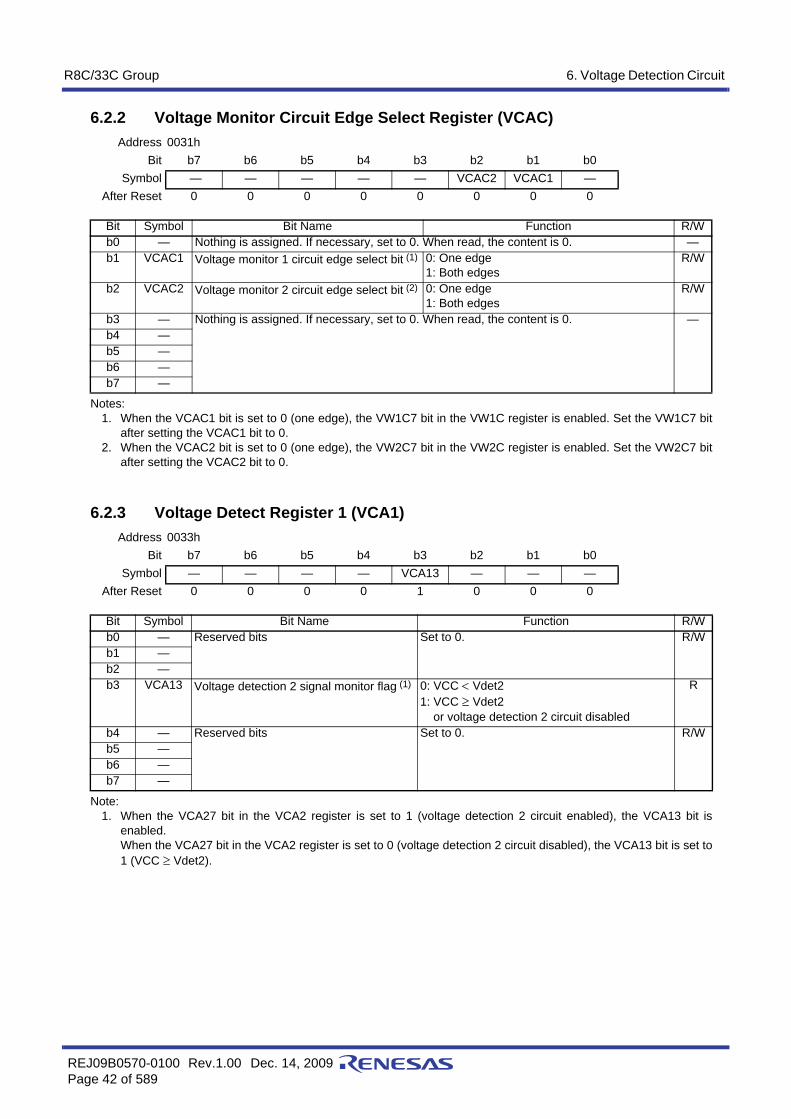
R8C/33C Group 6. Voltage Detection Circuit
REJ09B0570-0100 Rev.1.00 Dec. 14, 2009Page 42 of 589
6.2.2 Voltage Monitor Circuit Edge Select Register (VCAC)
Notes:1. When the VCAC1 bit is set to 0 (one edge), the VW1C7 bit in the VW1C register is enabled. Set the VW1C7 bit
after setting the VCAC1 bit to 0.2. When the VCAC2 bit is set to 0 (one edge), the VW2C7 bit in the VW2C register is enabled. Set the VW2C7 bit
after setting the VCAC2 bit to 0.
6.2.3 Voltage Detect Register 1 (VCA1)
Note:1. When the VCA27 bit in the VCA2 register is set to 1 (voltage detection 2 circuit enabled), the VCA13 bit is
enabled.When the VCA27 bit in the VCA2 register is set to 0 (voltage detection 2 circuit disabled), the VCA13 bit is set to1 (VCC ≥ Vdet2).
Address 0031hBit b7 b6 b5 b4 b3 b2 b1 b0
Symbol — — — — — VCAC2 VCAC1 —After Reset 0 0 0 0 0 0 0 0
Bit Symbol Bit Name Function R/Wb0 — Nothing is assigned. If necessary, set to 0. When read, the content is 0. —b1 VCAC1 Voltage monitor 1 circuit edge select bit (1) 0: One edge
1: Both edgesR/W
b2 VCAC2 Voltage monitor 2 circuit edge select bit (2) 0: One edge1: Both edges
R/W
b3 — Nothing is assigned. If necessary, set to 0. When read, the content is 0. —b4 —b5 —b6 —b7 —
Address 0033hBit b7 b6 b5 b4 b3 b2 b1 b0
Symbol — — — — VCA13 — — —After Reset 0 0 0 0 1 0 0 0
Bit Symbol Bit Name Function R/Wb0 — Reserved bits Set to 0. R/Wb1 —b2 —b3 VCA13 Voltage detection 2 signal monitor flag (1) 0: VCC < Vdet2
1: VCC ≥ Vdet2or voltage detection 2 circuit disabled
R
b4 — Reserved bits Set to 0. R/Wb5 —b6 —b7 —

R8C/33C Group 6. Voltage Detection Circuit
REJ09B0570-0100 Rev.1.00 Dec. 14, 2009Page 43 of 589
6.2.4 Voltage Detect Register 2 (VCA2)
Notes:1. Use the VCA20 bit only when the MCU enters wait mode. To set the VCA20 bit, follow the procedure shown in
Figure 9.3 Procedure for Reducing Internal Power Consumption Using VCA20 bit. 2. When the VCA20 bit is set to 1 (low consumption enabled), do not set the CM10 bit in the CM1 register to 1 (stop
mode).3. When writing to the VCA25 bit, set a value after reset.4. To use the voltage detection 1 interrupt or the VW1C3 bit in the VW1C register, set the VCA26 bit to 1.
After the VCA26 bit is set to 1 from 0, allow td(E-A) to elapse before the voltage detection 1 circuit startsoperation.
5. To use the voltage detection 2 interrupt or the VCA13 bit in the VCA1 register, set the VCA27 bit to 1.After the VCA27 bit is set to 1 from 0, allow td(E-A) to elapse before the voltage detection 2 circuit startsoperation.
Set the PRC3 bit in the PRCR register to 1 (write enabled) before rewriting the VCA2 register.
Address 0034hBit b7 b6 b5 b4 b3 b2 b1 b0
Symbol VCA27 VCA26 VCA25 — — — — VCA20After Reset 0 0 0 0 0 0 0 0
The above applies when the LVDAS bit in the OFS register is set to 1.After Reset 0 0 1 0 0 0 0 0
The above applies when the LVDAS bit in the OFS register is set to 0.
Bit Symbol Bit Name Function R/Wb0 VCA20 Internal power low consumption
enable bit (1)0: Low consumption disabled1: Low consumption enabled (2)
R/W
b1 — Reserved bits Set to 0. R/Wb2 —b3 —b4 —b5 VCA25 Voltage detection 0 enable bit (3) 0: Voltage detection 0 circuit disabled
1: Voltage detection 0 circuit enabledR/W
b6 VCA26 Voltage detection 1 enable bit (4) 0: Voltage detection 1 circuit disabled1: Voltage detection 1 circuit enabled
R/W
b7 VCA27 Voltage detection 2 enable bit (5) 0: Voltage detection 2 circuit disabled1: Voltage detection 2 circuit enabled
R/W

R8C/33C Group 6. Voltage Detection Circuit
REJ09B0570-0100 Rev.1.00 Dec. 14, 2009Page 44 of 589
6.2.5 Voltage Detection 1 Level Select Register (VD1LS)
Set the PRC3 bit in the PRCR register to 1 (write enabled) before rewriting the VD1LS register.
Address 0036hBit b7 b6 b5 b4 b3 b2 b1 b0
Symbol — — — — VD1S3 VD1S2 VD1S1 VD1S0After Reset 0 0 0 0 0 1 1 1
Bit Symbol Bit Name Function R/Wb0 VD1S0 Voltage detection 1 level select bit
(Reference voltage when the voltage falls) b3 b2 b1 b0 0 0 0 0: 2.20 V (Vdet1_0) 0 0 0 1: 2.35 V (Vdet1_1) 0 0 1 0: 2.50 V (Vdet1_2) 0 0 1 1: 2.65 V (Vdet1_3) 0 1 0 0: 2.80 V (Vdet1_4) 0 1 0 1: 2.95 V (Vdet1_5) 0 1 1 0: 3.10 V (Vdet1_6) 0 1 1 1: 3.25 V (Vdet1_7) 1 0 0 0: 3.40 V (Vdet1_8) 1 0 0 1: 3.55 V (Vdet1_9) 1 0 1 0: 3.70 V (Vdet1_A) 1 0 1 1: 3.85 V (Vdet1_B) 1 1 0 0: 4.00 V (Vdet1_C) 1 1 0 1: 4.15 V (Vdet1_D) 1 1 1 0: 4.30 V (Vdet1_E) 1 1 1 1: 4.45 V (Vdet1_F)
R/Wb1 VD1S1 R/Wb2 VD1S2 R/Wb3 VD1S3 R/W
b4 — Reserved bits Set to 0. R/Wb5 —b6 —b7 —

R8C/33C Group 6. Voltage Detection Circuit
REJ09B0570-0100 Rev.1.00 Dec. 14, 2009Page 45 of 589
6.2.6 Voltage Monitor 0 Circuit Control Register (VW0C)
Note:1. The VW0C0 bit is enabled when the VCA25 bit in the VCA2 register is set to 1 (voltage detection 0 circuit
enabled). When writing to the VW0C0 bit, set a value after reset.
Set the PRC3 bit in the PRCR register to 1 (write enabled) before writing the VW0C register.
Address 0038hBit b7 b6 b5 b4 b3 b2 b1 b0
Symbol — — — — — — — VW0C0After Reset 1 1 0 0 X 0 1 0
The above applies when the LVDAS bit in the OFS register is set to 1.After Reset 1 1 0 0 X 0 1 1
The above applies when the LVDAS bit in the OFS register is set to 0.
Bit Symbol Bit Name Function R/Wb0 VW0C0 Voltage monitor 0 reset enable bit (1) 0: Disabled
1: EnabledR/W
b1 — Reserved bit Set to 1. R/Wb2 — Reserved bit Set to 0. R/Wb3 — Reserved bit When read, the content is undefined. Rb4 — Reserved bits Set to 0. R/Wb5 —b6 — Reserved bits Set to 1. R/Wb7 —

R8C/33C Group 6. Voltage Detection Circuit
REJ09B0570-0100 Rev.1.00 Dec. 14, 2009Page 46 of 589
6.2.7 Voltage Monitor 1 Circuit Control Register (VW1C)
Notes:1. The VW1C0 is enabled when the VCA26 bit in the VCA2 register is set to 1 (voltage detection 1 circuit enabled).
Set the VW1C0 bit to 0 (disabled) when the VCA26 bit is set to 0 (voltage detection 1 circuit disabled).To set the VW0C0 bit to 1 (enabled), follow the procedure shown in Table 6.2 Procedure for Setting BitsAssociated with Voltage Monitor 1 Interrupt.
2. When using the digital filter (while the VW1C1 bit is 0), set the CM14 bit in the CM1 register to 0 (low-speed on-chip oscillator on).To use the voltage monitor 1 interrupt to exit stop mode, set the VW1C1 bit in the VW1C register to 1 (digital filterdisabled).
3. Bits VW1C2 and VW1C3 are enabled when the VCA26 bit in the VCA2 register is set to 1 (voltage detection 1circuit enabled).
4. Set the VW1C2 bit to 0 by a program. When 0 is written by a program, this bit is set to 0 (and remains unchangedeven if 1 is written to it).
5. The VW1C7 bit is enabled when the VCAC1 bit in the VCAC register is set to 0 (one edge). After setting theVCAC1 bit to 0, set the VW1C7 bit.
6. When the VW1C0 bit is set to 1 (enabled), do not set the VW1C1 bit and bits VW1F1 and VW1F0 simultaneously(with one instruction).
Set the PRC3 bit in the PRCR register to 1 (write enabled) before writing the VW1C register.Rewriting the VW1C register may set the VW1C2 bit to 1. Set the VW1C2 bit to 0 after rewriting the VW1Cregister.
Address 0039hBit b7 b6 b5 b4 b3 b2 b1 b0
Symbol VW1C7 — VW1F1 VW1F0 VW1C3 VW1C2 VW1C1 VW1C0After Reset 1 0 0 0 1 0 1 0
Bit Symbol Bit Name Function R/Wb0 VW1C0 Voltage monitor 1 reset interrupt enable
bit (1)0: Disabled1: Enabled
R/W
b1 VW1C1 Voltage monitor 1 digital filter disable mode select bit (2, 6)
0: Digital filter enabled mode (digital filter circuit enabled)
1: Digital filter disable mode (digital filter circuit disabled)
R/W
b2 VW1C2 Voltage change detection flag (3, 4) 0: Not detected1: Vdet1 passing detected
R/W
b3 VW1C3 Voltage detection 1 signal monitor flag (3) 0: VCC < Vdet11: VCC ≥ Vdet1
or voltage detection 1 circuit disabled
R
b4 VW1F0 Sampling clock select bit (6) b5 b4 0 0: fOCO-S divided by 1 0 1: fOCO-S divided by 2 1 0: fOCO-S divided by 4 1 1: fOCO-S divided by 8
R/Wb5 VW1F1 R/W
b6 — Reserved bit Set to 0. R/Wb7 VW1C7 Voltage monitor 1 interrupt
generation condition select bit (5)0: When VCC reaches Vdet1 or above.1: When VCC reaches Vdet1 or below.
R/W

R8C/33C Group 6. Voltage Detection Circuit
REJ09B0570-0100 Rev.1.00 Dec. 14, 2009Page 47 of 589
6.2.8 Voltage Monitor 2 Circuit Control Register (VW2C)
Notes:1. The VW2C0 is enabled when the VCA27 bit in the VCA2 register is set to 1 (voltage detection 2 circuit enabled).
Set the VW2C0 bit to 0 (disabled) when the VCA27 bit is set to 0 (voltage detection 2 circuit disabled). To set the VW2C0 bit to 1 (enabled), follow the procedure shown in Table 6.3 Procedure for Setting BitsAssociated with Voltage Monitor 2 Interrupt.
2. When using the digital filter (while the VW2C1 bit is 0), set the CM14 bit in the CM1 register to 0 (low-speed on-chip oscillator on).To use the voltage monitor 2 interrupt to exit stop mode, set the VW2C1 bit in the VW2C register to 1 (digital filterdisabled).
3. The VW2C2 bit is enabled when the VCA27 bit in the VCA2 register is set to 1 (voltage detection 2 circuitenabled).
4. Set this bit to 0 by a program. When 0 is written by a program, this bit is set to 0 (and remains unchanged even if1 is written to it).
5. The VW2C7 bit is enabled when the VCAC2 bit in the VCAC register is set to 0 (one edge). After setting theVCAC2 bit to 0, set the VW2C7 bit.
6. When the VW2C0 bit is set to 1 (enabled), do not set the VW2C1 bit and bits VW2F1 and VW2F0 simultaneously(with one instruction).
Set the PRC3 bit in the PRCR register to 1 (write enabled) before rewriting the VW2C register. Rewriting the VW2C register may set the VW2C2 bit to 1. After rewriting this register, set the VW2C2 bit to 0.
Address 003AhBit b7 b6 b5 b4 b3 b2 b1 b0
Symbol VW2C7 — VW2F1 VW2F0 VW2C3 VW2C2 VW2C1 VW2C0After Reset 1 0 0 0 0 0 1 0
Bit Symbol Bit Name Function R/Wb0 VW2C0 Voltage monitor 2 interrupt enable bit (1) 0: Disabled
1: EnabledR/W
b1 VW2C1 Voltage monitor 2 digital filterdisable mode select bit (2, 6)
0: Digital filter enable mode(digital filter circuit enabled)
1: Digital filter disable mode(digital filter circuit disabled)
R/W
b2 VW2C2 Voltage change detection flag (3, 4) 0: Not detected1: Vdet2 passing detected
R/W
b3 VW2C3 WDT detection monitor flag (4) 0: Not detected1: Detected
R/W
b4 VW2F0 Sampling clock select bit (6) b5 b4 0 0: fOCO-S divided by 1 0 1: fOCO-S divided by 2 1 0: fOCO-S divided by 4 1 1: fOCO-S divided by 8
R/Wb5 VW2F1 R/W
b6 — Reserved bit Set to 0. R/Wb7 VW2C7 Voltage monitor 2 interrupt
generation condition select bit (5)0: When VCC reaches Vdet2 or above. 1: When VCC reaches Vdet2 or below.
R/W

R8C/33C Group 6. Voltage Detection Circuit
REJ09B0570-0100 Rev.1.00 Dec. 14, 2009Page 48 of 589
6.2.9 Option Function Select Register (OFS)
Notes:1. The OFS register is allocated in the flash memory, not in the SFRs. Set appropriate values as ROM data by a
program.Do not write additions to the OFS register. If the block including the OFS register is erased, the OFS register isset to FFh.When blank products are shipped, the OFS register is set to FFh. It is set to the written value after written by theuser.When factory-programming products are shipped, the value of the OFS register is the value programmed by theuser.
2. The same level of the voltage detection 0 level selected by bits VDSEL0 and VDESL1 is set in both functions ofvoltage monitor 0 reset and power-on reset.
3. To use power-on reset and voltage monitor 0 reset, set the LVDAS bit to 0 (voltage monitor 0 reset enabled afterreset).
For a setting example of the OFS register, refer to 13.3.1 Setting Example of Option Function Select Area.
LVDAS Bit (Voltage Detection 0 Circuit Start Bit)The Vdet0 voltage to be monitored by the voltage detection 0 circuit is selected by bits VDSEL0 and VDSEL1.
Address 0FFFFhBit b7 b6 b5 b4 b3 b2 b1 b0
Symbol CSPROINI LVDAS VDSEL1 VDSEL0 ROMCP1 ROMCR — WDTONAfter Reset User Setting Value (1)
Bit Symbol Bit Name Function R/Wb0 WDTON Watchdog timer start select bit 0: Watchdog timer automatically starts after reset
1: Watchdog timer is stopped after resetR/W
b1 — Reserved bit Set to 1. R/Wb2 ROMCR ROM code protect disable bit 0: ROM code protect disabled
1: ROMCP1 bit enabledR/W
b3 ROMCP1 ROM code protect bit 0: ROM code protect enabled1: ROM code protect disabled
R/W
b4 VDSEL0 Voltage detection 0 level select bit (2) b5 b4 0 0: 3.80 V selected (Vdet0_3) 0 1: 2.85 V selected (Vdet0_2) 1 0: 2.35 V selected (Vdet0_1) 1 1: 1.90 V selected (Vdet0_0)
R/Wb5 VDSEL1 R/W
b6 LVDAS Voltage detection 0 circuit start bit (3) 0: Voltage monitor 0 reset enabled after reset1: Voltage monitor 0 reset disabled after reset
R/W
b7 CSPROINI Count source protection mode after reset select bit
0: Count source protect mode enabled after reset1: Count source protect mode disabled after reset
R/W

R8C/33C Group 6. Voltage Detection Circuit
REJ09B0570-0100 Rev.1.00 Dec. 14, 2009Page 49 of 589
6.3 VCC Input Voltage
6.3.1 Monitoring Vdet0Vdet0 cannot be monitored.
6.3.2 Monitoring Vdet1Once the following settings are made, the comparison result of voltage monitor 1 can be monitored by theVW1C3 bit in the VW1C register after td(E-A) has elapsed (refer to 32. Electrical Characteristics).
(1) Set bits VD1S3 to VD1S0 in the VD1LS register (voltage detection 1 detection voltage).(2) Set the VCA26 bit in the VCA2 register to 1 (voltage detection 1 circuit enabled).
6.3.3 Monitoring Vdet2Once the following settings are made, the comparison result of voltage monitor 2 can be monitored by theVCA13 bit in the VCA1 register after td(E-A) has elapsed (refer to 32. Electrical Characteristics).
• Set the VCA27 bit in the VCA2 register to 1 (voltage detection 2 circuit enabled).

R8C/33C Group 6. Voltage Detection Circuit
REJ09B0570-0100 Rev.1.00 Dec. 14, 2009Page 50 of 589
6.4 Voltage Monitor 0 ResetTo use voltage monitor 0 reset, set the LVDAS bit in the OFS register to 0 (voltage monitor 0 reset enabled afterreset).Figure 6.5 shows an Operating Example of Voltage Monitor 0 Reset.
Figure 6.5 Operating Example of Voltage Monitor 0 Reset
Vdet0
VCC
When the internal reset signal is driven low, the pins, CPU, and SFRs are initialized.When the internal reset signal level changes from low to high,a program is executed beginning with the address indicated by the reset vector.Refer to 4. Special Function Registers (SFRs) for the states of the SFRs after reset.
Internal reset signal
1fOCO-S × 32

R8C/33C Group 6. Voltage Detection Circuit
REJ09B0570-0100 Rev.1.00 Dec. 14, 2009Page 51 of 589
6.5 Voltage Monitor 1 InterruptTable 6.2 lists the Procedure for Setting Bits Associated with Voltage Monitor 1 Interrupt. Figure 6.6 shows anOperating Example of Voltage Monitor 1 Interrupt. To use the voltage monitor 1 interrupt to exit stop mode, set the VW1C1 bit in the VW1C register to 1 (digital filterdisabled).
Notes:1. When the VW1C0 bit is set to 0, steps 4 and 5 can be executed simultaneously (with one instruction).2. When the VW1C0 bit is set to 0, steps 6 and 7 can be executed simultaneously (with one instruction).3. When making the setting while the voltage monitor 1 interrupt is disabled (the VW1C0 bit in the
VW1C register is 0 and the VCA26 bit in the VCA2 register is 0), no interrupt request is generated if VCC < Vdet1 (or VCC > Vdet1) is detected before enabling the voltage monitor 1 interrupt in step 12.If VCC < Vdet1 (or VCC > Vdet1) is detected between step 10 and step 12, the VW1C2 bit is set to 1. Read the VW1C2 bit after step 12. If this bit is read as 1, perform the processing to be executed when the above state is detected.
Table 6.2 Procedure for Setting Bits Associated with Voltage Monitor 1 InterruptStep When Using Digital Filter When Using No Digital Filter
1 Select the voltage detection 1 detection voltage by bits VD1S3 to VD1S0 in the VD1LS register. 2 Set the VCA26 bit in the VCA2 register to 1 (voltage detection 1 circuit enabled).3 Wait for td(E-A).4 Set the COMPSEL bit in the CMPA register to 1.
5 (1) Select the interrupt type by the IRQ1SEL in the CMPA register.
6 Select the sampling clock of the digital filter by bits VW1F0 and VW1F1 in the VW1C register.
Set the VW1C1 bit in the VW1C register to 1 (digital filter disabled).
7 (2) Set the VW1C1 bit in the VW1C register to 0 (digital filter enabled).
−
8 Select the interrupt request timing by the VCAC1 bit in the VCAC register and the VW1C7 bit in the VW1C register.
9 Set the VW1C2 bit in the VW1C register to 0.
10 Set the CM14 bit in the CM1 register to 0 (low-speed on-chip oscillator on)
−
11 Wait for 2 cycles of the sampling clock of the digital filter
− (No wait time required)
12 (3) Set the VW1C0 bit in the VW1C register to 1 (voltage monitor 1 interrupt enabled)

R8C/33C Group 6. Voltage Detection Circuit
REJ09B0570-0100 Rev.1.00 Dec. 14, 2009Page 52 of 589
Figure 6.6 Operating Example of Voltage Monitor 1 Interrupt
Vdet1
VW1C3 bit
VCC
The above applies when: • VCA26 bit in VCA2 register = 1 (voltage detection 1 circuit enabled) • VW1C0 bit in VW1C register = 1 (voltage monitor 1 interrupt enabled)
Note: 1. If voltage monitor 0 reset is not used, set the power supply to VCC ≥ 1.8 V.
1.8 V (1)
Sampling clock ofdigital filter × 2 cycles
VW1C2 bit
VW1C2 bitVW1C1 bit is set to 1(digital filter disabled),VCAC1 bit is set to 0(one edge),andVW1C7 bit is set to 0(when VCC reaches Vdet1 or above)
VW1C1, VW1C2, VW1C3, VW1C7: Bits in VW1C registerVCAC1: Bit in VCAC register
Sampling clock ofdigital filter × 2 cycles
Set to 0 by a program.
Voltage monitor 1interrupt request
Voltage monitor 1interrupt request
Set to 0 when an interrupt requestis acknowledged.
VW1C2 bit
Voltage monitor 1interrupt request
VW1C1 bit is set to 0(digital filter enabled)andVCAC1 bit is set to 1(both edges)
VW1C2 bit
Set to 0 when an interrupt requestis acknowledged.
Set to 0 by a program.
Voltage monitor 1interrupt request
VW1C1 bit is set to 0(digital filter enabled),VCAC1 bit is set to 0(one edge),andVW1C7 bit is set to 0(when VCC reaches Vdet1 or above)
VW1C2 bit
Voltage monitor 1interrupt request
VW1C1 bit is set to 0(digital filter enabled),VCAC1 bit is set to 0(one edge),andVW1C7 bit is set to 1(when VCC reaches Vdet1 or below)
Set to 0 by a program.
VW1C2 bit
Voltage monitor 1interrupt request
VW1C1 bit is set to 1(digital filter disabled)andVCAC1 bit is set to 1(both edges)
Set to 0 by a program.
Set to 0 when an interrupt requestis acknowledged.
Set to 0 by a program.
Set to 0 when an interrupt requestis acknowledged.
Set to 0 by a program.VW1C1 bit is set to 1(digital filter disabled),VCAC1 bit is set to 0(one edge),andVW1C7 bit is set to 1(when VCC reaches Vdet1 or below)
Set to 0 when an interrupt requestis acknowledged.
Set to 0 when an interrupt requestis acknowledged.

R8C/33C Group 6. Voltage Detection Circuit
REJ09B0570-0100 Rev.1.00 Dec. 14, 2009Page 53 of 589
6.6 Voltage Monitor 2 InterruptTable 6.3 lists the Procedure for Setting Bits Associated with Voltage Monitor 2 Interrupt. Figure 6.7 shows anOperating Example of Voltage Monitor 2 Interrupt. To use the voltage monitor 2 interrupt to exit stop mode, set the VW2C1 bit in the VW2C register to 1 (digital filterdisabled).
Notes:1. When the VW2C0 bit is set to 0, steps 3 and 4 can be executed simultaneously (with one instruction).2. When the VW2C0 bit is set to 0, steps 5 and 6 can be executed simultaneously (with one instruction).3. When making the setting while the voltage monitor 2 interrupt is disabled (the VW2C0 bit in the
VW2C register is 0 and the VCA27 bit in the VCA2 register is 0), no interrupt request is generated if VCC < Vdet2 (or VCC > Vdet2) is detected before enabling the voltage monitor 2 interrupt in step 11. If VCC < Vdet2 (or VCC > Vdet2) is detected between step 9 and step 11, the VW2C2 bit is set to 1. Read the VW2C2 bit after step 11. If this bit is read as 1, perform the processing to be executed when the above state is detected.
Table 6.3 Procedure for Setting Bits Associated with Voltage Monitor 2 InterruptStep When Using Digital Filter When Using No Digital Filter
1 Set the VCA27 bit in the VCA2 register to 1 (voltage detection 2 circuit enabled).2 Wait for td(E-A).3 Set the COMPSEL bit in the CMPA register to 1.
4 (1) Select the interrupt type by the IRQ2SEL in the CMPA register.
5 Select the sampling clock of the digital filter by bits VW2F0 and VW2F1 in the VW2C register.
Set the VW2C1 bit in the VW2C register to 1 (digital filter disabled).
6 (2) Set the VW2C1 bit in the VW2C register to 0 (digital filter enabled).
−
7 Select the interrupt request timing by the VCAC2 bit in the VCAC register andthe VW2C7 bit in the VW2C register.
8 Set the VW2C2 bit in the VW2C register to 0.
9 Set the CM14 bit in the CM1 register to 0 (low-speed on-chip oscillator on).
−
10 Wait for 2 cycles of the sampling clock of the digital filter.
− (No wait time required)
11 (3) Set the VW2C0 bit in the VW2C register to 1 (voltage monitor 2 interrupt enabled).

R8C/33C Group 6. Voltage Detection Circuit
REJ09B0570-0100 Rev.1.00 Dec. 14, 2009Page 54 of 589
Figure 6.7 Operating Example of Voltage Monitor 2 Interrupt
Vdet2
VCA13 bit
VCC
The above applies when: • VCA27 bit in VCA2 register = 1 (voltage detection 2 circuit enabled) • VW2C0 bit in VW2C register = 1 (voltage monitor 2 interrupt enabled)
Note: 1. If voltage monitor 0 reset is not used, set the power supply to VCC ≥ 1.8 V.
1.8 V (1)
Sampling clock ofdigital filter × 2 cycles
VW2C2 bit
VW2C2 bit
VW2C1 bit is set to 1(digital filter disabled),VCAC2 bit is set to 0(one edge),andVW2C7 bit is set to 0(when VCC reachesVdet2 or above)
VCA13: Bit in VCA1 registerVW2C1, VW2C2, VW2C7: Bits in VW2C registerVCAC2: Bit in VCAC register
Sampling clock ofdigital filter × 2 cycles
Set to 0 by a program.
Voltage monitor 2interrupt request
Voltage monitor 2interrupt request
Set to 0 when an interrupt requestis acknowledged.
VW2C2 bit
Voltage monitor 2interrupt request
VW2C1 bit is set to 0(digital filter enabled)andVCAC2 bit is set to 1(both edges)
VW2C2 bit
Set to 0 when an interrupt requestis acknowledged.
Set to 0 by a program.
Voltage monitor 2interrupt request
VW2C1 bit is set to 0(digital filter enabled),VCAC2 bit is set to 0(one edge),andVW2C7 bit is set to 0(when VCC reachesVdet2 or above)
VW2C2 bit
Voltage monitor 2interrupt request
VW2C1 bit is set to 0(digital filter enabled),VCAC2 bit is set to 0(one edge),andVW2C7 bit is set to 1(when VCC reachesVdet2 or below)
Set to 0 by a program.
VW2C2 bit
Voltage monitor 2interrupt request
VW2C1 bit is set to 1(digital filter disabled)andVCAC2 bit is set to 1(both edges)
Set to 0 by a program.
Set to 0 when an interrupt requestis acknowledged.
Set to 0 by a program.
Set to 0 when an interrupt requestis acknowledged.
Set to 0 by a program.VW2C1 bit is set to 1(digital filter disabled),VCAC2 bit is set to 0(one edge),andVW2C7 bit is set to 1(when VCC reachesVdet2 or below)
Set to 0 when an interrupt requestis acknowledged.
Set to 0 when an interrupt requestis acknowledged.

R8C/33C Group 7. I/O Ports
REJ09B0570-0100 Rev.1.00 Dec. 14, 2009Page 55 of 589
7. I/O PortsThere are 27 I/O ports P0, P1, P2_0 to P2_2, P3_1, P3_3 to P3_5, P3_7, and P4_5 to P4_7 (P4_6 and P4_7 can be usedas I/O ports if the XIN clock oscillation circuit and the XCIN clock oscillation circuit are not used.). If the A/D converter and the D/A converter are not used, P4_2 can be used as an input-only port.Table 7.1 lists an Overview of I/O Ports.
Notes:1. In input mode, whether an internal pull-up resistor is connected or not can be selected by registers PUR0 and
PUR1.2. Whether the drive capacity of the output transistor is set to low or high can be selected using registers P1DRR
and P2DRR.3. Whether the drive capacity of the output transistor is set to low or high can be selected using registers DRR0
and DRR1.4. The input threshold value can be selected among three voltage levels (0.35 VCC, 0.50 VCC, and 0.70 VCC)
using registers VLT0 and VLT1.5. When the XIN clock oscillation circuit and the XCIN clock oscillation circuit are not used, these ports can be
used as I/O ports.6. When the A/D converter and the D/A converter are not used, this port can be used as an input-only ports.
7.1 Functions of I/O PortsThe PDi_j (j = 0 to 7) bit in the PDi (i = 0 to 4) register controls I/O of the ports P0, P1, P2_0 to P2_2, P3_1, P3_3to P3_5, P3_7, and P4_5 to P4_7. The Pi register consists of a port latch to hold output data and a circuit to read pinstates.Figures 7.1 to 7.10 show the Configurations of I/O Ports. Table 7.2 lists the Functions of I/O Ports.
i = 0 to 4, j = 0 to 7Note:
1. Nothing is assigned to bits PD4_0 to PD4_2.
Table 7.1 Overview of I/O Ports
Ports I/O Type of Output I/O Setting Internal Pull-Up Resister
Drive Capacity Switch Input Level Switch
P0 I/O CMOS3 state Set in 1-bit units Set in 4-bit units (1) Set in 4-bit units (3) Set in 8-bit units (4)
P1 I/O CMOS3 state Set in 1-bit units Set in 4-bit units (1) Set in 1-bit units (2) Set in 8-bit units (4)
P2_0 to P2_2 I/O CMOS3 state Set in 1-bit units Set in 3-bit units (1) Set in 1-bit units (2) Set in 3-bit units (4)
P3_1, P3_3 I/O CMOS3 state Set in 1-bit units Set in 2-bit units (1) Set in 2-bit units (3) Set in 5-bit units (4)
P3_4, P3_5, P3_7
I/O CMOS3 state Set in 1-bit units Set in 3-bit units (1) Set in 3-bit units (3)
P4_5, P4_6 (5), P4_7 (5)
I/O CMOS3 state Set in 1-bit units Set in 3-bit units (1) Set in 3-bit units (3) Set in 4-bit units (4)
P4_2 (6) I (No output function)
None None None
Table 7.2 Functions of I/O PortsOperation When
Accessing Pi Register
Value of PDi_j Bit in PDi Register (1)
When PDi_j Bit is Set to 0 (Input Mode) When PDi_j Bit is Set to 1 (Output Mode)
Read Read the pin input level. Read the port latch.
Write Write to the port latch. Write to the port latch. The value written to the port latch is output from the pin.

R8C/33C Group 7. I/O Ports
REJ09B0570-0100 Rev.1.00 Dec. 14, 2009Page 56 of 589
7.2 Effect on Peripheral FunctionsI/O ports function as I/O ports for peripheral functions (refer to Table 1.4 Pin Name Information by PinNumber).Table 7.3 lists the Setting of PDi_j Bit when Functioning as I/O Ports for Peripheral Functions (i = 0 to 4, j = 0 to7). Refer to the description of each function for information on how to set peripheral functions.
7.3 Pins Other than I/O PortsFigure 7.11 shows the Configuration of I/O Pins.
Table 7.3 Setting of PDi_j Bit when Functioning as I/O Ports for Peripheral Functions (i = 0 to 4, j = 0 to 7)
I/O of Peripheral Function PDi_j Bit Settings for Shared Pin FunctionInput Set this bit to 0 (input mode).Output This bit can be set to either 0 or 1 (output regardless of the port setting).

R8C/33C Group 7. I/O Ports
REJ09B0570-0100 Rev.1.00 Dec. 14, 2009Page 57 of 589
Figure 7.1 Configuration of I/O Ports (1)
Pin select register
P0_0 to P0_5
Drive capacity selection
(Note 1)
(Note 1)
Input to individual peripheral function
Analog input of A/D converter
P0_6 and P0_7
Drive capacity selection
(Note 1)
(Note 1)
Input to individual peripheral function
Analog input of A/D converter
Analog output of D/A converterD/A converteroutput enable
Note:1. symbolizes a parasitic diode.
Ensure the input voltage to each port does not exceed VCC.
Data bus
Pull-up selection
Output from individualperipheral function
Drive capacity selection
Input levelswitch function
Data bus
Pull-up selection
Output from individualperipheral function
Drive capacity selection
Input levelswitch function
Port latch
Directionregister Pin select
registerOutput from individual
peripheral function enabled
IOINSEL
Pin select register
Port latch
Directionregister Pin select
registerOutput from individual
peripheral function enabled
IOINSEL
IOINSEL: Bit in PINSR register

R8C/33C Group 7. I/O Ports
REJ09B0570-0100 Rev.1.00 Dec. 14, 2009Page 58 of 589
Figure 7.2 Configuration of I/O Ports (2)
IOINSEL: Bit in PINSR register
P1_0 to P1_3
Drive capacity selection
Input to individual peripheral function
Analog input of A/D converter
Note:1. symbolizes a parasitic diode.
Ensure the input voltage to each port does not exceed VCC.
(Note 1)
(Note 1)
Data bus
Pull-up selection
Output from individualperipheral function
Drive capacity selection
Input levelswitch function
Pin select register
Port latch
Directionregister Pin select
register
IOINSEL
Output from individualperipheral function enabled

R8C/33C Group 7. I/O Ports
REJ09B0570-0100 Rev.1.00 Dec. 14, 2009Page 59 of 589
Figure 7.3 Configuration of I/O Ports (3)
P1_5Drive capacity selection
Drive capacity selection
Input to individualperipheral function
Input to external interruptDigitalfilter
P1_4
Drive capacity selection
Input to individual peripheral function
(Note 1)
(Note 1)
(Note 1)
(Note 1)
Note:1. symbolizes a parasitic diode.
Ensure the input voltage to each port does not exceed VCC.
Data bus
Pull-up selection
Output from individualperipheral function
Drive capacity selection
Input levelswitch function
Data bus
Pull-up selection
Output from individualperipheral function
Input levelswitch function
IOINSEL: Bit in PINSR register
Pin select register
Port latch
Directionregister Pin select
register
IOINSEL
Output from individualperipheral function enabled
Pin select register
Port latch
Directionregister Pin select
register
IOINSEL
Output from individualperipheral function enabled

R8C/33C Group 7. I/O Ports
REJ09B0570-0100 Rev.1.00 Dec. 14, 2009Page 60 of 589
Figure 7.4 Configuration of I/O Ports (4)
IOINSEL: Bit in PINSR register
P1_7 Drive capacity selection
Drive capacity selection
Input to individualperipheral function
Input to external interruptDigitalfilter
Analog input ofcomparator B
Drive capacity selection
Drive capacity selection
Input to individual peripheral function
Analog input of comparator B
P1_6
(Note 1)
(Note 1)
(Note 1)
(Note 1)
Note:1. symbolizes a parasitic diode.
Ensure the input voltage to each port does not exceed VCC.
Data bus
Pull-up selection
Output from individualperipheral function
Input levelswitch function
Data bus
Pull-up selection
Output from individualperipheral function
Input levelswitch function
Pin select register
Port latch
Directionregister
IOINSEL
Output from individualperipheral function enabled
Pin selectregister
Pin select register
Port latch
Directionregister Pin select
register
IOINSEL
Output from individualperipheral function enabled

R8C/33C Group 7. I/O Ports
REJ09B0570-0100 Rev.1.00 Dec. 14, 2009Page 61 of 589
Figure 7.5 Configuration of I/O Ports (5)
P2_0 Drive capacity selection
Drive capacity selection
Input to individualperipheral function
Input to external interruptDigitalfilter
(Note 1)
(Note 1)
Note:1. symbolizes a parasitic diode.
Ensure the input voltage to each port does not exceed VCC.
Data bus
Pull-up selection
Output from individualperipheral function
Input levelswitch function
P2_1 to P2_2Drive capacity selection
Drive capacity selection
Input to individual peripheral function
(Note 1)
(Note 1)
Data bus
Pull-up selection
Output from individualperipheral function
Input levelswitch function
IOINSEL: Bit in PINSR register
Pin select register
Port latch
Directionregister
IOINSEL
Output from individualperipheral function enabled
Pin selectregister
Pin select register
Port latch
Directionregister Pin select
register
IOINSEL
Output from individualperipheral function enabled

R8C/33C Group 7. I/O Ports
REJ09B0570-0100 Rev.1.00 Dec. 14, 2009Page 62 of 589
Figure 7.6 Configuration of I/O Ports (6)
Drive capacity selection
Drive capacity selection
P3_1
(Note 1)
(Note 1)
Data bus
Pull-up selection
Output from individualperipheral function
Input levelswitch function
P3_3
Drive capacity selection
Input to individualperipheral function
Input to external interruptDigitalfilter
Analog input ofcomparator B
(Note 1)
(Note 1)
Data bus
Pull-up selection
Output from individualperipheral function
Input levelswitch function
Drive capacity selection
Note:1. symbolizes a parasitic diode.
Ensure the input voltage to each port does not exceed VCC.
Port latch
Directionregister Pin select
register
IOINSEL
Output from individualperipheral function enabled
IOINSEL: Bit in PINSR register
Pin select register
Port latch
Directionregister Pin select
register
IOINSEL
Output from individualperipheral function enabled

R8C/33C Group 7. I/O Ports
REJ09B0570-0100 Rev.1.00 Dec. 14, 2009Page 63 of 589
Figure 7.7 Configuration of I/O Ports (7)
Note:1. symbolizes a parasitic diode.
Ensure the input voltage to each port does not exceed VCC.
P3_5
Drive capacity selection
Input to individual peripheral function
(Note 1)
(Note 1)
Data bus
Pull-up selection
Output from individualperipheral function
Input levelswitch function
Drive capacity selection
Drive capacity selection
Drive capacity selection
Input to individual peripheral function
Analog input of comparator B
P3_4
(Note 1)
(Note 1)
Data bus
Pull-up selection
Output from individualperipheral function
Input levelswitch function
Pin select register
Port latch
Directionregister Pin select
register
IOINSEL
Output from individualperipheral function enabled
IOINSEL: Bit in PINSR register
Pin select register
Port latch
Directionregister Pin select
register
IOINSEL
Output from individualperipheral function enabled

R8C/33C Group 7. I/O Ports
REJ09B0570-0100 Rev.1.00 Dec. 14, 2009Page 64 of 589
Figure 7.8 Configuration of I/O Ports (8)
Note:1. symbolizes a parasitic diode.
Ensure the input voltage to each port does not exceed VCC.
P3_7Drive capacity selection
Drive capacity selection
Input to individualperipheral function
(Note 1)
(Note 1)
Data bus
Pull-up selection
Output from individualperipheral function
Input levelswitch function
IOINSEL: Bit in PINSR register
Pin select register
Port latch
Directionregister
IOINSEL
Output from individualperipheral function enabled
Pin selectregister

R8C/33C Group 7. I/O Ports
REJ09B0570-0100 Rev.1.00 Dec. 14, 2009Page 65 of 589
Figure 7.9 Configuration of I/O Ports (9)
IOINSEL: Bit in PINSR register
P4_2/VREF
Data bus Input levelswitch function
(Note 1)
(Note 1)
P4_5 Drive capacity selection
Drive capacity selection
(Note 1)
(Note 1)
Input to individualperipheral function
Input to external interruptA/D trigger input
Digitalfilter
Note:1. symbolizes a parasitic diode.
Ensure the input voltage to each port does not exceed VCC.
Data bus
Pull-up selection
Output from individualperipheral function
Input levelswitch function
Pin select register
Port latch
Directionregister
IOINSEL
Output from individualperipheral function enabled
Pin selectregister

R8C/33C Group 7. I/O Ports
REJ09B0570-0100 Rev.1.00 Dec. 14, 2009Page 66 of 589
Figure 7.10 Configuration of I/O Ports (10)
Note:1. symbolizes a parasitic diode.
Ensure the input voltage to each port does not exceed VCC.
CM01, CM03, CM04, CM05: Bits in CM0 registerCM11, CM12, CM13: Bits in CM1 registerIOINSEL: Bit in PINSR register
CM05
CM11
CM13
RfXIN
XINoscillation
circuit CM03
CM12
RfXCIN
XCINoscillationcircuit
CM04, CM130 1
CM01
0 1
CM01
Data bus
Pull-up selection
Drive capacity selection
Drive capacity selection
Input levelswitch function
P4_6/XIN/XCIN
Data bus
Pull-up selection
Drive capacity selection
Drive capacity selection
Input levelswitch function
P4_7/XOUT/XCOUT
(Note 1)
(Note 1)
(Note 1)
(Note 1)
Port latch
Directionregister
IOINSEL
Port latch
Directionregister
IOINSEL

R8C/33C Group 7. I/O Ports
REJ09B0570-0100 Rev.1.00 Dec. 14, 2009Page 67 of 589
Figure 7.11 Configuration of I/O Pins
MODE
RESET
(Note 1)
(Note 1)
(Note 1)
Note:1. symbolizes a parasitic diode.
Ensure the input voltage to each port does not exceed VCC.
MODE signal input
RESET signal input

R8C/33C Group 7. I/O Ports
REJ09B0570-0100 Rev.1.00 Dec. 14, 2009Page 68 of 589
7.4 Registers
7.4.1 Port Pi Direction Register (PDi) (i = 0 to 4)
Notes:1. Write to the PD0 register with the next instruction after that used to set the PRC2 bit in the PRCR register to 1
(write enabled).2. Bits PD2_3 to PD2_7 in the PD2 register are reserved bits. If it is necessary to set bits PD2_3 and PD2_7, set to
0. When read, the content is 0.3. Bits PD3_0, PD3_2, and PD3_6 in the PD3 register are reserved bits. If it is necessary to set bits PD3_0, PD3_2
and PD3_6, set to 0. When read, the content is 0.4. Bits PD4_0 to PD4_2 in the PD4 register are unavailable on this MCU. If it is necessary to set bits PD4_0 to
PD4_2 set to 0. When read, the content is 0. Bits PD4_3, PD4_4 are reserved bits. If it is necessary to set bitsPD4_3 and PD4_4, set to 0. When read, the content is 0.
The PDi register selects whether I/O ports are used for input or output. Each bit in the PDi register correspondsto one port.
Address 00E2h (PD0 (1)), 00E3h (PD1), 00E6h (PD2 (2)), 00E7h (PD3 (3)), 00EAh (PD4 (4))Bit b7 b6 b5 b4 b3 b2 b1 b0
Symbol PDi_7 PDi_6 PDi_5 PDi_4 PDi_3 PDi_2 PDi_1 PDi_0After Reset 0 0 0 0 0 0 0 0
Bit Symbol Bit Name Function R/Wb0 PDi_0 Port Pi_0 direction bit 0: Input mode (functions as an input port)
1: Output mode (functions as an output port)R/W
b1 PDi_1 Port Pi_1 direction bit R/Wb2 PDi_2 Port Pi_2 direction bit R/Wb3 PDi_3 Port Pi_3 direction bit R/Wb4 PDi_4 Port Pi_4 direction bit R/Wb5 PDi_5 Port Pi_5 direction bit R/Wb6 PDi_6 Port Pi_6 direction bit R/Wb7 PDi_7 Port Pi_7 direction bit R/W

R8C/33C Group 7. I/O Ports
REJ09B0570-0100 Rev.1.00 Dec. 14, 2009Page 69 of 589
7.4.2 Port Pi Register (Pi) (i = 0 to 4)
Notes:1. Bits P2_3 to P2_7 in the P2 register are reserved bits. If it is necessary to set bits P2_3 and P2_7, set to 0. When
read, the content is 0.2. Bits P3_0, P3_2, and P3_6 in the P3 register are reserved bits. If it is necessary to set bits P3_0, P3_2 and
P3_6, set to 0. When read, the content is 0.3. Bits P4_0 to P4_1 in the P4 register are unavailable on this MCU. If it is necessary to set bits P4_0 to P4_1 set to
0. When read, the content is 0. Bits P4_3, P4_4 are reserved bits. If it is necessary to set bits P4_3 and P4_4, setto 0. When read, the content is 0.
Data input and output to and from external devices are accomplished by reading and writing to the Pi register.The Pi register consists of a port latch to retain output data and a circuit to read the pin status. The value writtenin the port latch is output from the pin. Each bit in the Pi register corresponds to one port.
Pi_j Bit (i = 0 to 4, j = 0 to 7) (Port Pi_j Bit)The pin level of any I/O port which is set to input mode can be read by reading the corresponding bit in thisregister. The pin level of any I/O port which is set to output mode can be controlled by writing to thecorresponding bit in this register.
Address 00E0h(P0), 00E1h(P1), 00E4h(P2 (1)), 00E5h(P3 (2)), 00E8h(P4 (3))Bit b7 b6 b5 b4 b3 b2 b1 b0
Symbol Pi_7 Pi_6 Pi_5 Pi_4 Pi_3 Pi_2 Pi_1 Pi_0After Reset X X X X X X X X
Bit Symbol Bit Name Function R/Wb0 Pi_0 Port Pi_0 bit 0: “L” level
1: “H” levelR/W
b1 Pi_1 Port Pi_1 bit R/Wb2 Pi_2 Port Pi_2 bit R/Wb3 Pi_3 Port Pi_3 bit R/Wb4 Pi_4 Port Pi_4 bit R/Wb5 Pi_5 Port Pi_5 bit R/Wb6 Pi_6 Port Pi_6 bit R/Wb7 Pi_7 Port Pi_7 bit R/W

R8C/33C Group 7. I/O Ports
REJ09B0570-0100 Rev.1.00 Dec. 14, 2009Page 70 of 589
7.4.3 Timer RA Pin Select Register (TRASR)
The TRASR register selects which pin is assigned to the timer RA I/O. To use the I/O pin for timer RA, set thisregister. Set the TRASR register before setting the timer RA associated registers. Also, do not change the setting valuein this register during timer RA operation.
7.4.4 Timer RB/RC Pin Select Register (TRBRCSR)
The TRBRCSR register selects which pin is assigned to the timer RB and timer RC I/O. To use the I/O pin fortimer RB and timer RC, set this register. Set the TRBOSEL0 bit before setting the timer RB associated registers. Set bits TRCCLKSEL0 andTRCCLKSEL1 before setting the timer RC associated registers. Also, do not change the setting values of theTRBOSEL0 bit during timer RB operation. Do not change the setting values of bits TRCCLKSEL0 andTRCCLKSEL1 during timer RC operation.
Address 0180hBit b7 b6 b5 b4 b3 b2 b1 b0
Symbol — — — — — — TRAIOSEL1 TRAIOSEL0After Reset 0 0 0 0 0 0 0 0
Bit Symbol Bit Name Function R/Wb0 TRAIOSEL0 TRAIO pin select bit b1 b0
0 0: TRAIO pin not used 0 1: P1_7 assigned 1 0: P1_5 assigned 1 1: Do not set.
R/Wb1 TRAIOSEL1 R/W
b2 — Reserved bits Set to 0. R/Wb3 —b4 —b5 — Nothing is assigned. If necessary, set to 0. When read, the content is 0. —b6 —b7 —
Address 0181hBit b7 b6 b5 b4 b3 b2 b1 b0
Symbol — — TRCCLKSEL1 TRCCLKSEL0 — — — TRBOSEL0After Reset 0 0 0 0 0 0 0 0
Bit Symbol Bit Name Function R/Wb0 TRBOSEL0 TRBO pin select bit 0: P1_3 assigned
1: P3_1 assignedR/W
b1 — Reserved bit Set to 0. R/Wb2 — Nothing is assigned. If necessary, set to 0. When read, the content is 0. —b3 —b4 TRCCLKSEL0 TRCCLK pin select bit b5 b4
0 0: TRCCLK pin not used 0 1: P1_4 assigned 1 0: P3_3 assigned 1 1: Do not set.
R/Wb5 TRCCLKSEL1 R/W
b6 — Reserved bit Set to 0. R/Wb7 — Nothing is assigned. If necessary, set to 0. When read, the content is 0. —

R8C/33C Group 7. I/O Ports
REJ09B0570-0100 Rev.1.00 Dec. 14, 2009Page 71 of 589
7.4.5 Timer RC Pin Select Register 0 (TRCPSR0)
The TRCPSR0 register selects which pin is assigned to the timer RC I/O. To use the I/O pin for timer RC, setthis register. Set the TRCPSR0 register before setting the timer RC associated registers. Also, do not change the setting valuein this register during timer RC operation.
Address 0182hBit b7 b6 b5 b4 b3 b2 b1 b0
Symbol — TRCIOBSEL2 TRCIOBSEL1 TRCIOBSEL0 — TRCIOASEL2 TRCIOASEL1 TRCIOASEL0After Reset 0 0 0 0 0 0 0 0
Bit Symbol Bit Name Function R/Wb0 TRCIOASEL0 TRCIOA/TRCTRG pin select bit b2 b1 b0
0 0 0: TRCIOA/TRCTRG pin not used 0 0 1: P1_1 assigned 0 1 0: P0_0 assigned 0 1 1: P0_1 assigned 1 0 0: P0_2 assignedOther than above: Do not set.
R/Wb1 TRCIOASEL1 R/Wb2 TRCIOASEL2 R/W
b3 — Nothing is assigned. If necessary, set to 0. When read, the content is 0. —b4 TRCIOBSEL0 TRCIOB pin select bit b6 b5 b4
0 0 0: TRCIOB pin not used 0 0 1: P1_2 assigned 0 1 0: P0_3 assigned 0 1 1: P0_4 assigned 1 0 0: P0_5 assigned 1 0 1: P2_0 assignedOther than above: Do not set.
R/Wb5 TRCIOBSEL1 R/Wb6 TRCIOBSEL2 R/W
b7 — Nothing is assigned. If necessary, set to 0. When read, the content is 0. —

R8C/33C Group 7. I/O Ports
REJ09B0570-0100 Rev.1.00 Dec. 14, 2009Page 72 of 589
7.4.6 Timer RC Pin Select Register 1 (TRCPSR1)
The TRCPSR1 register selects which pin is assigned to the timer RC I/O. To use the I/O pin for timer RC, setthis register. Set the TRCPSR1 register before setting the timer RC associated registers. Also, do not change the setting valuein this register during timer RC operation.
Address 0183hBit b7 b6 b5 b4 b3 b2 b1 b0
Symbol — TRCIODSEL2 TRCIODSEL1 TRCIODSEL0 — TRCIOCSEL2 TRCIOCSEL1 TRCIOCSEL0After Reset 0 0 0 0 0 0 0 0
Bit Symbol Bit Name Function R/Wb0 TRCIOCSEL0 TRCIOC pin select bit b2 b1 b0
0 0 0: TRCIOC pin not used 0 0 1: P1_3 assigned 0 1 0: P3_4 assigned 0 1 1: P0_7 assigned 1 0 0: P2_1 assignedOther than above: Do not set.
R/Wb1 TRCIOCSEL1 R/Wb2 TRCIOCSEL2 R/W
b3 — Nothing is assigned. If necessary, set to 0. When read, the content is 0. —b4 TRCIODSEL0 TRCIOD pin select bit b6 b5 b4
0 0 0: TRCIOD pin not used 0 0 1: P1_0 assigned 0 1 0: P3_5 assigned 0 1 1: P0_6 assigned 1 0 0: P2_2 assignedOther than above: Do not set.
R/Wb5 TRCIODSEL1 R/Wb6 TRCIODSEL2 R/W
b7 — Nothing is assigned. If necessary, set to 0. When read, the content is 0. —

R8C/33C Group 7. I/O Ports
REJ09B0570-0100 Rev.1.00 Dec. 14, 2009Page 73 of 589
7.4.7 UART0 Pin Select Register (U0SR)
The U0SR register selects which pin is assigned to the UART0 I/O. To use the I/O pin for UART0, set thisregister. Set the U0SR register before setting the UART0 associated registers. Also, do not change the setting value inthis register during UART0 operation.
7.4.8 UART1 Pin Select Register (U1SR)
The U1SR register selects which pin is assigned to the UART1 I/O. To use the I/O pin for UART1, set thisregister. Set the U1SR register before setting the UART1 associated registers. Also, do not change the setting value inthis register during UART1 operation.
Address 0188hBit b7 b6 b5 b4 b3 b2 b1 b0
Symbol — — — CLK0SEL0 — RXD0SEL0 — TXD0SEL0After Reset 0 0 0 0 0 0 0 0
Bit Symbol Bit Name Function R/Wb0 TXD0SEL0 TXD0 pin select bit 0: TXD0 pin not used
1: P1_4 assignedR/W
b1 — Nothing is assigned. If necessary, set to 0. When read, the content is 0. —b2 RXD0SEL0 RXD0 pin select bit 0: RXD0 pin not used
1: P1_5 assignedR/W
b3 — Nothing is assigned. If necessary, set to 0. When read, the content is 0. —b4 CLK0SEL0 CLK0 pin select bit 0: CLK0 pin not used
1: P1_6 assignedR/W
b5 — Nothing is assigned. If necessary, set to 0. When read, the content is 0. —b6 —b7 —
Address 0189hBit b7 b6 b5 b4 b3 b2 b1 b0
Symbol — — — CLK1SEL0 — RXD1SEL0 — TXD1SEL0After Reset 0 0 0 0 0 0 0 0
Bit Symbol Bit Name Function R/Wb0 TXD1SEL0 TXD1 pin select bit 0: TXD1 pin not used
1: P0_1 assignedR/W
b1 — Reserved bit Set to 0. R/Wb2 RXD1SEL0 RXD1 pin select bit 0: RXD1 pin not used
1: P0_2 assignedR/W
b3 — Reserved bit Set to 0. R/Wb4 CLK1SEL0 CLK1 pin select bit 0: CLK1 pin not used
1: P0_3 assignedR/W
b5 — Reserved bit Set to 0. R/Wb6 — Nothing is assigned. If necessary, set to 0. When read, the content is 0. —b7 —

R8C/33C Group 7. I/O Ports
REJ09B0570-0100 Rev.1.00 Dec. 14, 2009Page 74 of 589
7.4.9 UART2 Pin Select Register 0 (U2SR0)
The U2SR0 register selects which pin is assigned to the UART2 I/O. To use the I/O pin for UART2, set thisregister. Set the U2SR0 register before setting the UART2 associated registers. Also, do not change the setting value inthis register during UART2 operation.
7.4.10 UART2 Pin Select Register 1 (U2SR1)
The U2SR1 register selects which pin is assigned to the UART2 I/O. To use the I/O pin for UART2, set thisregister. Set the U2SR1 register before setting the UART2 associated registers. Also, do not change the setting value inthis register during UART2 operation.
Address 018AhBit b7 b6 b5 b4 b3 b2 b1 b0
Symbol — — RXD2SEL1 RXD2SEL0 — — TXD2SEL1 TXD2SEL0After Reset 0 0 0 0 0 0 0 0
Bit Symbol Bit Name Function R/Wb0 TXD2SEL0 TXD2/SDA2 pin select bit b1 b0
0 0: TXD2/SDA2 pin not used 0 1: P3_7 assigned 1 0: P3_4 assigned 1 1: Do not set.
R/Wb1 TXD2SEL1 R/W
b2 — Reserved bit Set to 0. R/Wb3 — Nothing is assigned. If necessary, set to 0. When read, the content is 0. —b4 RXD2SEL0 RXD2/SCL2 pin select bit b5 b4
0 0: RXD2/SCL2 pin not used 0 1: P3_4 assigned 1 0: P3_7 assigned 1 1: P4_5 assigned
R/Wb5 RXD2SEL1 R/W
b6 — Reserved bit Set to 0. R/Wb7 — Nothing is assigned. If necessary, set to 0. When read, the content is 0. —
Address 018BhBit b7 b6 b5 b4 b3 b2 b1 b0
Symbol — — — CTS2SEL0 — — — CLK2SEL0After Reset 0 0 0 0 0 0 0 0
Bit Symbol Bit Name Function R/Wb0 CLK2SEL0 CLK2 pin select bit 0: CLK2 pin not used
1: P3_5 assignedR/W
b1 — Reserved bit Set to 0. R/Wb2 — Nothing is assigned. If necessary, set to 0. When read, the content is 0. —b3 —b4 CTS2SEL0 CTS2/RTS2 pin select bit 0: CTS2/RTS2 pin not used
1: P3_3 assignedR/W
b5 — Reserved bit Set to 0. R/Wb6 — Nothing is assigned. If necessary, set to 0. When read, the content is 0. —b7 —
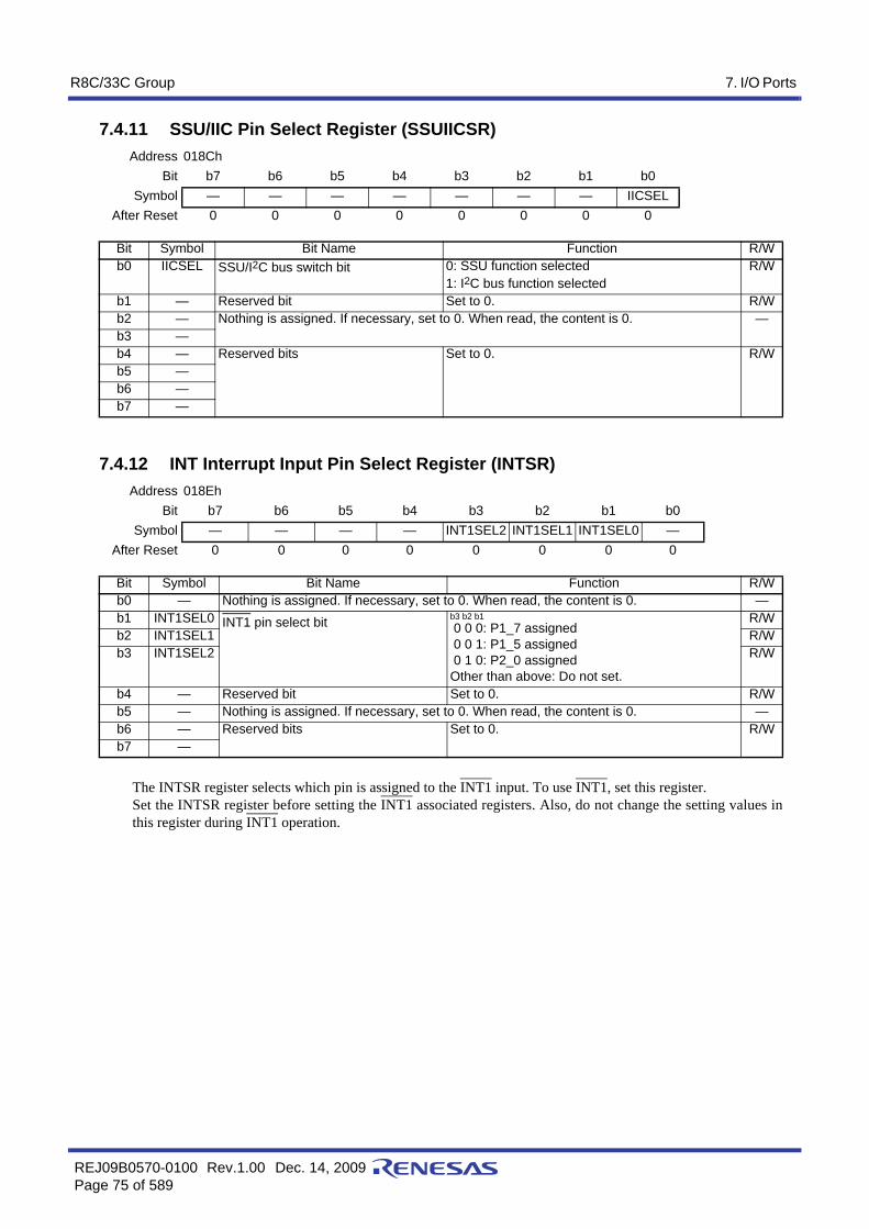
R8C/33C Group 7. I/O Ports
REJ09B0570-0100 Rev.1.00 Dec. 14, 2009Page 75 of 589
7.4.11 SSU/IIC Pin Select Register (SSUIICSR)
7.4.12 INT Interrupt Input Pin Select Register (INTSR)
The INTSR register selects which pin is assigned to the INT1 input. To use INT1, set this register. Set the INTSR register before setting the INT1 associated registers. Also, do not change the setting values inthis register during INT1 operation.
Address 018ChBit b7 b6 b5 b4 b3 b2 b1 b0
Symbol — — — — — — — IICSELAfter Reset 0 0 0 0 0 0 0 0
Bit Symbol Bit Name Function R/Wb0 IICSEL SSU/I2C bus switch bit 0: SSU function selected
1: I2C bus function selectedR/W
b1 — Reserved bit Set to 0. R/Wb2 — Nothing is assigned. If necessary, set to 0. When read, the content is 0. —b3 —b4 — Reserved bits Set to 0. R/Wb5 —b6 —b7 —
Address 018EhBit b7 b6 b5 b4 b3 b2 b1 b0
Symbol — — — — INT1SEL2 INT1SEL1 INT1SEL0 —After Reset 0 0 0 0 0 0 0 0
Bit Symbol Bit Name Function R/Wb0 — Nothing is assigned. If necessary, set to 0. When read, the content is 0. —b1 INT1SEL0 INT1 pin select bit b3 b2 b1
0 0 0: P1_7 assigned 0 0 1: P1_5 assigned 0 1 0: P2_0 assignedOther than above: Do not set.
R/Wb2 INT1SEL1 R/Wb3 INT1SEL2 R/W
b4 — Reserved bit Set to 0. R/Wb5 — Nothing is assigned. If necessary, set to 0. When read, the content is 0. —b6 — Reserved bits Set to 0. R/Wb7 —

R8C/33C Group 7. I/O Ports
REJ09B0570-0100 Rev.1.00 Dec. 14, 2009Page 76 of 589
7.4.13 I/O Function Pin Select Register (PINSR)
IOINSEL Bit (I/O port input function select bit)The IOINSEL bit is used to select the pin level of an I/O port when the PDi_j (j = 0 to 7) bit in the PDi (i = 0 to4) register is set to 1 (output mode). When this bit is set to 1, the I/O port input function reads the pin input levelregardless of the PDi register.
Table 7.4 lists I/O Port Values Read by Using IOINSEL Bit. The IOINSEL bit can be used to change the inputfunction of all I/O ports except P4_2.
Address 018FhBit b7 b6 b5 b4 b3 b2 b1 b0
Symbol SDADLY1 SDADLY0 IICTCHALF IICTCTWI IOINSEL — — —After Reset 0 0 0 0 0 0 0 0
Bit Symbol Bit Name Function R/Wb0 — Reserved bit Set to 0. R/Wb1 — R/Wb2 — Nothing is assigned. If necessary, set to 0. When read, the content is 0. —b3 IOINSEL I/O port input function select bit 0: The I/O port input function depends on the PDi (i =
0 to 4) register.When the PDi_j (j = 0 to 7) bit in the PDi register is set to 0 (input mode), the pin input level is read. When the PDi_j bit in the PDi register is set to 1 (output mode), the port latch is read.
1: The I/O port input function reads the pin input level regardless of the PDi register.
R/W
b4 IICTCTWI I2C double transfer rate select bit 0: Transfer rate is the same as the value set with bits CKS0 to CKS3 in the ICCR1 register
1: Transfer rate is twice the value set with bits CKS0 to CKS3 in the ICCR1 register
R/W
b5 IICTCHALF I2C half transfer rate select bit 0: Transfer rate is the same as the value set with bits CKS0 to CKS3 in the ICCR1 register
1: Transfer rate is half the value set with bits CKS0 to CKS3 in the ICCR1 register
R/W
b6 SDADLY0 SDA digital delay select bit b7 b6 0 0: Digital delay of 3 × f1 cycles 0 1: Digital delay of 11 × f1 cycles 1 0: Digital delay of 19 × f1 cycles 1 1: Do not set.
R/Wb7 SDADLY1 R/W
Table 7.4 I/O Port Values Read by Using IOINSEL BitPDi_j bit in PDi register 0 (input mode) 1 (output mode)
IOINSEL bit 0 1 0 1I/O port values read Pin input level Port latch value Pin input level

R8C/33C Group 7. I/O Ports
REJ09B0570-0100 Rev.1.00 Dec. 14, 2009Page 77 of 589
7.4.14 Pull-Up Control Register 0 (PUR0)
Note:1. When this bit is set to 1 (pulled up), the pin whose port direction bit is set to 0 (input mode) is pulled up.
For pins used as input, the setting values in the PUR0 register are valid.
7.4.15 Pull-Up Control Register 1 (PUR1)
Note:1. When this bit is set to 1 (pulled up), the pin whose port direction bit is set to 0 (input mode) is pulled up.
For pins used as input, the setting values in the PUR1 register are valid.
Address 01E0hBit b7 b6 b5 b4 b3 b2 b1 b0
Symbol PU07 PU06 — PU04 PU03 PU02 PU01 PU00After Reset 0 0 0 0 0 0 0 0
Bit Symbol Bit Name Function R/Wb0 PU00 P0_0 to P0_3 pull-up 0: Not pulled up
1: Pulled up (1)R/W
b1 PU01 P0_4 to P0_7 pull-up R/Wb2 PU02 P1_0 to P1_3 pull-up R/Wb3 PU03 P1_4 to P1_7 pull-up R/Wb4 PU04 P2_0 to P2_2 pull-up R/Wb5 — Reserved bit Set to 0. R/Wb6 PU06 P3_1, P3_3 pull-up 0: Not pulled up
1: Pulled up (1)R/W
b7 PU07 P3_4, P3_5, P3_7 pull-up R/W
Address 01E1hBit b7 b6 b5 b4 b3 b2 b1 b0
Symbol — — — — — — PU11 —After Reset 0 0 0 0 0 0 0 0
Bit Symbol Bit Name Function R/Wb0 — Reserved bit Set to 0. R/Wb1 PU11 P4_5 to P4_7 pull-up 0: Not pulled up
1: Pulled up (1)R/W
b2 — Reserved bits Set to 0. R/Wb3 —b4 —b5 —b6 — Nothing is assigned. If necessary, set to 0. When read, the content is undefined. —b7 —

R8C/33C Group 7. I/O Ports
REJ09B0570-0100 Rev.1.00 Dec. 14, 2009Page 78 of 589
7.4.16 Port P1 Drive Capacity Control Register (P1DRR)
Note:1. Both “H” and “L” output are set to high drive capacity.
The P1DRR register selects whether the drive capacity of the P1 output transistor is set to low or high. The P1DRRi bit (i = 0 to 7) is used to select whether the drive capacity of the output transistor is set to low orhigh for each pin.For pins used as output, the setting values in the P1DRR register are valid.
7.4.17 Port P2 Drive Capacity Control Register (P2DRR)
Note:1. Both “H” and “L” output are set to high drive capacity.
The P2DRR register selects whether the drive capacity of the P2_0 to P2_2 output transistor is set to low orhigh. The P2DRRi bit (i = 0 to 2) is used to select whether the drive capacity of the output transistor is set to lowor high for each pin.For pins used as output, the setting values in the P2DRR register are valid.
Address 01F0hBit b7 b6 b5 b4 b3 b2 b1 b0
Symbol P1DRR7 P1DRR6 P1DRR5 P1DRR4 P1DRR3 P1DRR2 P1DRR1 P1DRR0After Reset 0 0 0 0 0 0 0 0
Bit Symbol Bit Name Function R/Wb0 P1DRR0 P1_0 drive capacity 0: Low
1: High (1)R/W
b1 P1DRR1 P1_1 drive capacity R/Wb2 P1DRR2 P1_2 drive capacity R/Wb3 P1DRR3 P1_3 drive capacity R/Wb4 P1DRR4 P1_4 drive capacity R/Wb5 P1DRR5 P1_5 drive capacity R/Wb6 P1DRR6 P1_6 drive capacity R/Wb7 P1DRR7 P1_7 drive capacity R/W
Address 01F1hBit b7 b6 b5 b4 b3 b2 b1 b0
Symbol — — — — — P2DRR2 P2DRR1 P2DRR0After Reset 0 0 0 0 0 0 0 0
Bit Symbol Bit Name Function R/Wb0 P2DRR0 P2_0 drive capacity 0: Low
1: High (1)R/W
b1 P2DRR1 P2_1 drive capacity R/Wb2 P2DRR2 P2_2 drive capacity R/Wb3 — Reserved bits Set to 0. R/Wb4 —b5 —b6 —b7 —

R8C/33C Group 7. I/O Ports
REJ09B0570-0100 Rev.1.00 Dec. 14, 2009Page 79 of 589
7.4.18 Drive Capacity Control Register 0 (DRR0)
Note:1. Both “H” and “L” output are set to high drive capacity.
For pins used as output, the setting values in the DRR0 register are valid.
DRR00 Bit (P0_0 to P0_3 drive capacity)The DRR00 bit selects whether the drive capacity of the P0_0 to P0_3 output transistors is set to low or high.This bit is used to select whether the drive capacity of the output transistors is set to low or high for four pins.
DRR01 Bit (P0_4 to P0_7 drive capacity)The DRR01 bit selects whether the drive capacity of the P0_4 to P0_7 output transistors is set to low or high.This bit is used to select whether the drive capacity of the output transistors is set to low or high for four pins.
DRR06 Bit (P3_1, P3_3 drive capacity)The DRR06 bit selects whether the drive capacity of the P3_1, P3_3 output transistors is set to low or high. Thisbit is used to select whether the drive capacity of the output transistors is set to low or high for two pins.
DRR07 Bit (P3_4, P3_5, P3_7 drive capacity)The DRR07 bit selects whether the drive capacity of the P3_4, P3_5, P3_7 output transistors is set to low orhigh. This bit is used to select whether the drive capacity of the output transistors is set to low or high for threepins.
Address 01F2hBit b7 b6 b5 b4 b3 b2 b1 b0
Symbol DRR07 DRR06 — — — — DRR01 DRR00After Reset 0 0 0 0 0 0 0 0
Bit Symbol Bit Name Function R/Wb0 DRR00 P0_0 to P0_3 drive capacity 0: Low
1: High (1)R/W
b1 DRR01 P0_4 to P0_7 drive capacity R/Wb2 — Nothing is assigned. If necessary, set to 0. When read, the content is 0. —b3 —b4 —b5 —b6 DRR06 P3_1, P3_3 drive capacity 0: Low
1: High (1)R/W
b7 DRR07 P3_4, P3_5, P3_7 drive capacity R/W
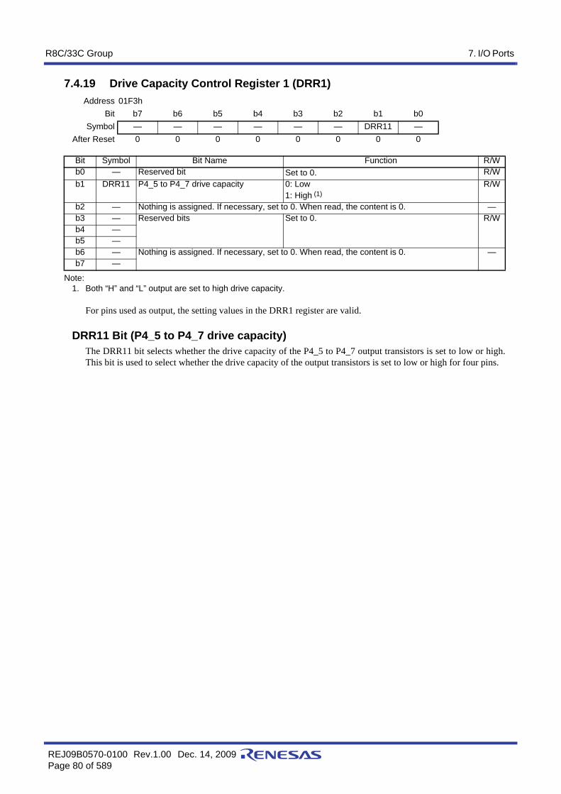
R8C/33C Group 7. I/O Ports
REJ09B0570-0100 Rev.1.00 Dec. 14, 2009Page 80 of 589
7.4.19 Drive Capacity Control Register 1 (DRR1)
Note:1. Both “H” and “L” output are set to high drive capacity.
For pins used as output, the setting values in the DRR1 register are valid.
DRR11 Bit (P4_5 to P4_7 drive capacity)The DRR11 bit selects whether the drive capacity of the P4_5 to P4_7 output transistors is set to low or high.This bit is used to select whether the drive capacity of the output transistors is set to low or high for four pins.
Address 01F3hBit b7 b6 b5 b4 b3 b2 b1 b0
Symbol — — — — — — DRR11 —After Reset 0 0 0 0 0 0 0 0
Bit Symbol Bit Name Function R/Wb0 — Reserved bit Set to 0. R/Wb1 DRR11 P4_5 to P4_7 drive capacity 0: Low
1: High (1)R/W
b2 — Nothing is assigned. If necessary, set to 0. When read, the content is 0. —b3 — Reserved bits Set to 0. R/Wb4 —b5 —b6 — Nothing is assigned. If necessary, set to 0. When read, the content is 0. —b7 —

R8C/33C Group 7. I/O Ports
REJ09B0570-0100 Rev.1.00 Dec. 14, 2009Page 81 of 589
7.4.20 Input Threshold Control Register 0 (VLT0)
The VLT0 register selects the voltage level of the input threshold values for ports P0, P1, P2_0 to P2_2, P3_1,P3_3 to P3_5, P3_7. Bits VLT00 to VLT07 are used to select the input threshold values among three voltagelevels (0.35 VCC, 0.50 VCC, and 0.70 VCC).
Address 01F5hBit b7 b6 b5 b4 b3 b2 b1 b0
Symbol VLT07 VLT06 VLT05 VLT04 VLT03 VLT02 VLT01 VLT00After Reset 0 0 0 0 0 0 0 0
Bit Symbol Bit Name Function R/Wb0 VLT00 P0 input level select bit b1 b0
0 0: 0.50 × VCC 0 1: 0.35 × VCC 1 0: 0.70 × VCC 1 1: Do not set.
R/Wb1 VLT01 R/W
b2 VLT02 P1 input level select bit b3 b2 0 0: 0.50 × VCC 0 1: 0.35 × VCC 1 0: 0.70 × VCC 1 1: Do not set.
R/Wb3 VLT03 R/W
b4 VLT04 P2_0 to P2_2 input level select bit b5 b4 0 0: 0.50 × VCC 0 1: 0.35 × VCC 1 0: 0.70 × VCC 1 1: Do not set.
R/Wb5 VLT05 R/W
b6 VLT06 P3_1, P3_3 to P3_5, P3_7 input level select bit
b7 b6 0 0: 0.50 × VCC 0 1: 0.35 × VCC 1 0: 0.70 × VCC 1 1: Do not set.
R/Wb7 VLT07 R/W

R8C/33C Group 7. I/O Ports
REJ09B0570-0100 Rev.1.00 Dec. 14, 2009Page 82 of 589
7.4.21 Input Threshold Control Register 1 (VLT1)
The VLT1 register selects the voltage level of the input threshold values for ports P4_2 and P4_5 to P4_7. BitsVLT10 to VLT15 are used to select the input threshold values among three voltage levels (0.35 VCC, 0.50VCC, and 0.70 VCC).
Address 01F6hBit b7 b6 b5 b4 b3 b2 b1 b0
Symbol — — — — — — VLT11 VLT10After Reset 0 0 0 0 0 0 0 0
Bit Symbol Bit Name Function R/Wb0 VLT10 P4_2, P4_5 to P4_7 input level select
bitb1 b0 0 0: 0.50 × VCC 0 1: 0.35 × VCC 1 0: 0.70 × VCC 1 1: Do not set.
R/Wb1 VLT11 R/W
b2 — Reserved bits Set to 0. R/Wb3 —b4 —b5 —b6 — Nothing is assigned. If necessary, set to 0. When read, the content is 0. —b7 —

R8C/33C Group 7. I/O Ports
REJ09B0570-0100 Rev.1.00 Dec. 14, 2009Page 83 of 589
7.5 Port SettingsTables 7.5 to 7.37 list the port settings.
X: 0 or 1Notes:
1. Pulled up by setting the PU00 bit in the PUR0 register to 1.2. Output drive capacity high by setting the DRR00 bit in the DRR0 register to 1.
X: 0 or 1Notes:
1. Pulled up by setting the PU00 bit in the PUR0 register to 1.2. Output drive capacity high by setting the DRR00 bit in the DRR0 register to 1.3. N-channel open-drain output by setting the NCH bit in the U1C0 register to 1.
X: 0 or 1Notes:
1. Pulled up by setting the PU00 bit in the PUR0 register to 1.2. Output drive capacity high by setting the DRR00 bit in the DRR0 register to 1.
Table 7.5 Port P0_0/AN7/TRCIOA/TRCTRGRegister PD0 ADINSEL TRCPSR0 Timer RC Setting
FunctionBit PD0_0
CH ADGSEL TRCIOASEL—
2 1 0 1 0 2 1 0
Setting Value
0 X X X X X Other than 010b X Input port (1)
1 X X X X X Other than 010b X Output port (2)
0 1 1 1 0 0 Other than 010b X A/D converter input (AN7) (1)
0 X X X X X 0 1 0 Refer to Table 7.34 TRCIOA Pin Setting TRCIOA input (1)
X X X X X X 0 1 0 Refer to Table 7.34 TRCIOA Pin Setting TRCIOA output (2)
Table 7.6 Port P0_1/AN6/TXD1/TRCIOA/TRCTRGRegister PD0 ADINSEL U1SR U1MR TRCPSR0 Timer RC Setting
FunctionBit PD0_1
CH ADGSELTXD1SEL0
SMD TRCIOASEL—
2 1 0 1 0 2 1 0 2 1 0
Setting Value
0 X X X X X 0 X X X Other than 011b X Input port (1)
1 X X X X X 0 X X X Other than 011b X Output port (2)
0 1 1 0 0 0 0 X X X Other than 011b X A/D converter input (AN6) (1)
X X X X X X 1
00
1
X X X X TXD1 output (2, 3)1
01
1 0
0 X X X X X 0 X X X 0 1 1 Refer to Table 7.34 TRCIOA Pin Setting TRCIOA input (1)
X X X X X X 0 X X X 0 1 1 Refer to Table 7.34 TRCIOA Pin Setting TRCIOA output (2)
Table 7.7 Port P0_2/AN5/RXD1/TRCIOA/TRCTRGRegister PD0 ADINSEL U1SR TRCPSR0 Timer RC Setting
FunctionBit PD0_2
CH ADGSELRXD1SEL0
TRCIOASEL—
2 1 0 1 0 2 1 0
Setting Value
0 X X X X X X Other than 100b X Input port (1)
1 X X X X X X Other than 100b X Output port (2)
0 1 0 1 0 0 0 Other than 100b X A/D converter input (AN5) (1)
0 X X X X X 1 Other than 100b X RXD1 input (1)
0 X X X X X X 1 0 0 Refer to Table 7.34 TRCIOA Pin Setting TRCIOA input (1)
X X X X X X X 1 0 0 Refer to Table 7.34 TRCIOA Pin Setting TRCIOA output (2)

R8C/33C Group 7. I/O Ports
REJ09B0570-0100 Rev.1.00 Dec. 14, 2009Page 84 of 589
X: 0 or 1Notes:
1. Pulled up by setting the PU00 bit in the PUR0 register to 1.2. Output drive capacity high by setting the DRR00 bit in the DRR0 register to 1.
X: 0 or 1Notes:
1. Pulled up by setting the PU01 bit in the PUR0 register to 1.2. Output drive capacity high by setting the DRR01 bit in the DRR0 register to 1.
X: 0 or 1Notes:
1. Pulled up by setting the PU01 bit in the PUR0 register to 1.2. Output drive capacity high by setting the DRR01 bit in the DRR0 register to 1.
Table 7.8 Port P0_3/AN4/CLK1/TRCIOBRegister PD0 ADINSEL U1SR U1MR TRCPSR0 Timer RC Setting
FunctionBit PD0_3
CH ADGSELCLK1SEL0
SMDCKDIR
TRCIOBSEL—
2 1 0 1 0 2 1 0 2 1 0
Setting Value
0 X X X X X 0 X X X X Other than 010b X Input port (1)
1 X X X X X 0 X X X X Other than 010b X Output port (2)
0 1 0 0 0 0 0 X X X X Other than 010b X
A/D converter input (AN4) (1)
0 X X X X X 1 X X X 1 X X X XCLK1 (external clock) input (1)
X X X X X X 1 0 0 1 0 X X X XCLK1 (internal clock) output (2)
0 X X X X X 0 X X X X 0 1 0 Refer to Table 7.35 TRCIOB Pin Setting TRCIOB input (1)
X X X X X X 0 X X X X 0 1 0 Refer to Table 7.35 TRCIOB Pin Setting TRCIOB output (2)
Table 7.9 Port P0_4/AN3/TREO/TRCIOBRegister PD0 ADINSEL TRECR1 TRCPSR0 Timer RC Setting
FunctionBit PD0_4
CH ADGSELTOENA
TRCIOBSEL—
2 1 0 1 0 2 1 0
Setting Value
0 X X X X X 0 Other than 011b X Input port (1)
1 X X X X X 0 Other than 011b X Output port (2)
0 0 1 1 0 0 0 Other than 011b X A/D converter input (AN3) (1)
X X X X X X 1 Other than 011b X TREO output (2)
0 X X X X X X 0 1 1 Refer to Table 7.35 TRCIOB Pin Setting TRCIOB input (1)
X X X X X X X 0 1 1 Refer to Table 7.35 TRCIOB Pin Setting TRCIOB output (2)
Table 7.10 Port P0_5/AN2/TRCIOBRegister PD0 ADINSEL TRCPSR0 Timer RC Setting
FunctionBit PD0_5
CH ADGSEL TRCIOBSEL—
2 1 0 1 0 2 1 0
Setting Value
0 X X X X X Other than 100b X Input port (1)
1 X X X X X Other than 100b X Output port (2)
0 0 1 0 0 0 Other than 100b X A/D converter input (AN2) (1)
0 X X X X X 1 0 0 Refer to Table 7.35 TRCIOB Pin Setting TRCIOB input (1)
X X X X X X 1 0 0 Refer to Table 7.35 TRCIOB Pin Setting TRCIOB output (2)

R8C/33C Group 7. I/O Ports
REJ09B0570-0100 Rev.1.00 Dec. 14, 2009Page 85 of 589
X: 0 or 1Notes:
1. Pulled up by setting the PU01 bit in the PUR0 register to 1.2. Output drive capacity high by setting the DRR01 bit in the DRR0 register to 1.
X: 0 or 1Notes:
1. Pulled up by setting the PU01 bit in the PUR0 register to 1.2. Output drive capacity high by setting the DRR01 bit in the DRR0 register to 1.
X: 0 or 1Notes:
1. Pulled up by setting the PU02 bit in the PUR0 register to 1.2. Output drive capacity high by setting the P1DRR0 bit in the P1DRR register to 1.
Table 7.11 Port P0_6/AN1/DA0/TRCIODRegister PD0 ADINSEL DACON TRCPSR1 Timer RC Setting
FunctionBit PD0_6
CH ADGSELDA0E
TRCIODSEL—
2 1 0 1 0 2 1 0
Setting Value
0 X X X X X 0 Other than 011b X Input port (1)
1 X X X X X 0 Other than 011b X Output port (2)
0 0 0 1 0 0 0 Other than 011b X A/D converter input (AN1) (1)
0 X X X X X 1 Other than 011b X D/A converter output (DA0) (1)
0 X X X X X 0 0 1 1 Refer to Table 7.37 TRCIOD Pin Setting TRCIOD input (1)
X X X X X X 0 0 1 1 Refer to Table 7.37 TRCIOD Pin Setting TRCIOD output (2)
Table 7.12 Port P0_7/AN0/DA1/TRCIOCRegister PD0 ADINSEL DACON TRCPSR1 Timer RC Setting
FunctionBit PD0_7
CH ADGSELDA1E
TRCIOCSEL—
2 1 0 1 0 2 1 0
Setting Value
0 X X X X X 0 Other than 011b X Input port (1)
1 X X X X X 0 Other than 011b X Output port (2)
0 0 0 0 0 0 0 Other than 011b X A/D converter input (AN0) (1)
0 X X X X X 1 Other than 011b X D/A converter output (DA1) (1)
0 X X X X X 0 0 1 1 Refer to Table 7.36 TRCIOC Pin Setting TRCIOC input (1)
X X X X X X 0 0 1 1 Refer to Table 7.36 TRCIOC Pin Setting TRCIOC output (2)
Table 7.13 Port P1_0/KI0/AN8/TRCIODRegister PD1 KIEN ADINSEL TRCPSR1 Timer RC Setting
FunctionBit PD1_0 KI0EN
CH ADGSEL TRCIODSEL—
2 1 0 1 0 2 1 0
Setting Value
0 X X X X X X Other than 001b X Input port (1)
1 X X X X X X Other than 001b X Output port (2)
0 1 X X X X X Other than 001b X KI0 input (1)
0 0 0 0 0 0 1 Other than 001b X A/D converter input (AN8) (1)
0 X X X X X X 0 0 1 Refer to Table 7.37 TRCIOD Pin Setting TRCIOD input (1)
X X X X X X X 0 0 1 Refer to Table 7.37 TRCIOD Pin Setting TRCIOD output (2)

R8C/33C Group 7. I/O Ports
REJ09B0570-0100 Rev.1.00 Dec. 14, 2009Page 86 of 589
X: 0 or 1Notes:
1. Pulled up by setting the PU02 bit in the PUR0 register to 1.2. Output drive capacity high by setting the P1DRR1 bit in the P1DRR register to 1.
X: 0 or 1Notes:
1. Pulled up by setting the PU02 bit in the PUR0 register to 1.2. Output drive capacity high by setting the P1DRR2 bit in the P1DRR register to 1.
Table 7.14 Port P1_1/KI1/AN9/TRCIOA/TRCTRGRegister PD1 KIEN ADINSEL TRCPSR0 Timer RC Setting
FunctionBit PD1_1 KI1EN
CH ADGSEL TRCIOASEL—
2 1 0 1 0 2 1 0
Setting Value
0 X X X X X X Other than 001b X Input port (1)
1 X X X X X X Other than 001b X Output port (2)
0 1 X X X X X Other than 001b X KI1 input (1)
0 0 0 0 1 0 1 Other than 001b X A/D converter input (AN9) (1)
0 X X X X X X 0 0 1 Refer to Table 7.34 TRCIOA Pin Setting TRCIOA input (1)
X X X X X X X 0 0 1 Refer to Table 7.34 TRCIOA Pin Setting TRCIOA output (2)
Table 7.15 Port P1_2/KI2/AN10/TRCIOBRegister PD1 KIEN ADINSEL TRCPSR0 Timer RC Setting
FunctionBit PD1_2 KI2EN
CH ADGSEL TRCIOBSEL—
2 1 0 1 0 2 1 0
Setting Value
0 X X X X X X Other than 001b X Input port (1)
1 X X X X X X Other than 001b X Output port (2)
0 1 X X X X X Other than 001b X KI2 input (1)
0 0 0 1 0 0 1 Other than 001b X A/D converter input (AN10) (1)
0 X X X X X X 0 0 1 Refer to Table 7.35 TRCIOB Pin Setting TRCIOB input (1)
X X X X X X X 0 0 1 Refer to Table 7.35 TRCIOB Pin Setting TRCIOB output (2)

R8C/33C Group 7. I/O Ports
REJ09B0570-0100 Rev.1.00 Dec. 14, 2009Page 87 of 589
X: 0 or 1Notes:
1. Pulled up by setting the PU02 bit in the PUR0 register to 1.2. Output drive capacity high by setting the P1DRR3 bit in the P1DRR register to 1.
X: 0 or 1Notes:
1. Pulled up by setting the PU03 bit in the PUR0 register to 1.2. Output drive capacity high by setting the P1DRR4 bit in the P1DRR register to 1.3. N-channel open-drain output by setting the NCH bit in the U0C0 register to 1.
Table 7.16 Port P1_3/KI3/AN11/TRCIOCRegister PD1 KIEN ADINSEL TRBRCSR TRCPSR1 Timer RB Setting Timer RC Setting
FunctionBit PD1_3 KI3EN
CH ADGSELTRBOSEL0
TRCIOCSEL— —
2 1 0 1 0 2 1 0
Setting Value
0 X X X X X X1
Other than 001b
XX Input port (1)
X Other than TRBO usage conditions
1 X X X X X X1
Other than 001b
XX Output port (2)
X Other than TRBO usage conditions
0 1 X X X X X1
Other than 001b
XX KI3 input (1)
X Other than TRBO usage conditions
0 0 0 1 1 0 11
Other than 001b
XX A/D converter
input (AN11) (1)X Other than TRBO usage conditions
X X X X X X X 0 X X XRefer to Table 7.33 TRBO Pin
SettingX TRBO output (2)
0 X X X X X X1
0 0 1X
Refer to Table 7.36 TRCIOC Pin Setting TRCIOC input (1)
X Other than TRBO usage conditions
X X X X X X X1
0 0 1X
Refer to Table 7.36 TRCIOC Pin Setting TRCIOC output (2)
X Other than TRBO usage conditions
Table 7.17 Port P1_4/TXD0/TRCCLKRegister PD1 U0SR U0MR TRBRCSR TRCCR1
FunctionBit PD1_4 TXD0SEL0
SMD TRCCLKSEL TCK2 1 0 1 0 2 1 0
Setting Value
0 0 X X X X X X X X Input port (1)
1 0 X X X X X X X X Output port (2)
X 1
00
1
X X X X X TXD0 output (2, 3)1
01
1 00 0 X X X 0 1 1 0 1 TRCCLK input (1)

R8C/33C Group 7. I/O Ports
REJ09B0570-0100 Rev.1.00 Dec. 14, 2009Page 88 of 589
X: 0 or 1Notes:
1. Pulled up by setting the PU03 bit in the PUR0 register to 1.2. Output drive capacity high by setting the P1DRR5 bit in the P1DRR register to 1.
X: 0 or 1Notes:
1. Pulled up by setting the PU03 bit in the PUR0 register to 1.2. Output drive capacity high by setting the P1DRR6 bit in the P1DRR register to 1.
Table 7.18 Port P1_5/RXD0/TRAIO/INT1Register PD1 U0SR TRASR TRAIOC TRAMR INTSR INTEN INTCMP
FunctionBit PD1_5 RXD0SEL0
TRAIOSELTOPCR
TMOD INT1SELINT1EN INT1CP0
1 0 2 1 0 2 1 0
Setting Value
0 X Other than 10b X X X X X X X X X Input port (1)
1 X Other than 10b X X X X X X X X X Output port (2)
0 1 Other than 10b X X X X X X X X X RXD0 input (1)
0 X 1 0 0 Other than 000b, 001b X X X X X TRAIO input (1)
0 X Other than 10b X X X X 0 0 1 1 0 INT1 input (1)
0 X 1 0 0 Other than 000b, 001b 0 0 1 1 0 TRAIO/INT1 input (1)
X X 1 0 0 0 0 1 X X X X XTRAIO pulse output (2)
0 1 1 0 0Master mode: 000bSlave mode: 011b
X X X X X TRAIO/RXD0 input (Hardware LIN)
0 1 1 0 0 0 0 1 1 0TRAIO/RXD0/INT1 input (Hardware LIN)
Table 7.19 Port P1_6/CLK0/IVREF1Register PD1 U0SR U0MR INTCMP
FunctionBit PD1_6 CLK0SEL0
SMDCKDIR INT1CP0
2 1 0
Setting Value
0 0 X X X X X Input port (1)
1 0 X X X X X Output port (2)
0 1 X X X 1 X CLK0 (external clock) input (1)
X 1 0 0 1 0 X CLK0 (internal clock) output (2)
0 0 X X X X 1 Comparator B1 reference voltage input (IVREF1)

R8C/33C Group 7. I/O Ports
REJ09B0570-0100 Rev.1.00 Dec. 14, 2009Page 89 of 589
X: 0 or 1Notes:
1. Pulled up by setting the PU03 bit in the PUR0 register to 1.2. Output drive capacity high by setting the P1DRR7 bit in the P1DRR register to 1.
X: 0 or 1Notes:
1. Pulled up by setting the PU04 bit in the PUR0 register to 1.2. Output drive capacity high by setting the P2DRR0 bit in the P2DRR register to 1.
X: 0 or 1Notes:
1. Pulled up by setting the PU04 bit in the PUR0 register to 1.2. Output drive capacity high by setting the P2DRR1 bit in the P2DRR register to 1.
Table 7.20 Port P1_7/INT1/TRAIO/IVCMP1Register PD1 TRASR TRAIOC TRAMR INTSR INTEN INTCMP
FunctionBit PD1_7
TRAIOSELTOPCR
TMOD INT1SELINT1EN INT1CP0
1 0 2 1 0 2 1 0
Setting Value
0 Other than 01b X X X X X X X X X Input port (1)
1 Other than 01b X X X X X X X X X Output port (2)
0 0 1 0 Other than 000b, 001b X X X X X TRAIO input (1)
0 Other than 01b X X X X 0 0 0 1 0 INT1 input (1)
0 0 1 0 Other than 000b, 001b 0 0 0 1 0 TRAIO/INT1 input (1)
X 0 1 0 0 0 1 X X X X X TRAIO pulse output (2)
0 Other than 01b X X X X X X X 1 1 Comparator B1 input (IVCMP1)
Table 7.21 Port P2_0/INT1/TRCIOBRegister PD2 INTSR INTEN INTCMP TRCPSR0 Timer RC Setting
FunctionBit PD2_0
INT1SELINT1EN INT1CP0
TRCIOBSEL—
2 1 0 2 1 0
Setting Value
0 X X X X X Other than 101b X Input port (1)
1 X X X X X Other than 101b X Output port (2)
0 0 1 0 1 0 Other than 101b X INT1 input (1)
0 X X X X X 1 0 1 Refer to Table 7.35 TRCIOB Pin Setting TRCIOB input (1)
X X X X X X 1 0 1 Refer to Table 7.35 TRCIOB Pin Setting TRCIOB output (2)
Table 7.22 Port P2_1/TRCIOCRegister PD2 TRCPSR1 Timer RC Setting
FunctionBit PD2_1
TRCIOCSEL—
2 1 0
Setting Value
0 Other than 100b X Input port (1)
1 Other than 100b X Output port (2)
0 1 0 0 Refer to Table 7.36 TRCIOC Pin Setting TRCIOC input (1)
X 1 0 0 Refer to Table 7.36 TRCIOC Pin Setting TRCIOC output (2)

R8C/33C Group 7. I/O Ports
REJ09B0570-0100 Rev.1.00 Dec. 14, 2009Page 90 of 589
X: 0 or 1Notes:
1. Pulled up by setting the PU04 bit in the PUR0 register to 1.2. Output drive capacity high by setting the P2DRR2 bit in the P2DRR register to 1.
X: 0 or 1Notes:
1. Pulled up by setting the PU06 bit in the PUR0 register to 1.2. Output drive capacity high by setting the DRR06 bit in the DRR0 register to 1.
X: 0 or 1Notes:
1. Pulled up by setting the PU06 bit in the PUR0 register to 1.2. Output drive capacity high by setting the DRR06 bit in the DRR0 register to 1.3. N-channel open-drain output by setting the CSOS bit in the SSMR2 register to 1 (N-channel open-drain output).
Table 7.23 Port P2_2/TRCIODRegister PD2 TRCPSR1 Timer RC Setting
FunctionBit PD2_2
TRCIODSEL—
2 1 0
Setting Value
0 Other than 100b X Input port (1)
1 Other than 100b X Output port (2)
0 1 0 0 Refer to Table 7.37 TRCIOD Pin Setting TRCIOD input (1)
X 1 0 0 Refer to Table 7.37 TRCIOD Pin Setting TRCIOD output (2)
Table 7.24 Port P3_1/TRBORegister PD3 TRBRCSR Timer RB Setting
FunctionBit PD3_1 TRBOSEL0 —
Setting Value
0 0 X Input port (1)
1 0 X Output port (2)
X 1 Refer to Table 7.33 TRBO Pin Setting TRBO output (2)
Table 7.25 Port P3_3/INT3/TRCCLK/SCS/CTS2/RTS2/IVCMP3Register PD3 SSMR2 INTEN TRBRCSR TRCCR1 U2SR1 U2MR U2CO INTCMP
FunctionBit PD3_3
CSSINT3EN
TRCCLKSEL TCKCTS2SEL0
SMDCRS CRD INT3CP0
1 0 1 0 2 1 0 2 1 0
Setting Value
0 0 0 X X X X X X 0 X X X X X X Input port (1)
1 0 0 X X X X X X 0 X X X X X X Output port (2)
0 0 0 1 X X X X X 0 X X X X X 0 INT3 input (1)
0 0 0 X 1 0 1 0 1 0 X X X X X X TRCCLK input (1)
X 0 1 X X X X X X X X X X X SCS input (1)
X1 0
X X X X X X X X X X X SCS output (2, 3)1 1
0 0 0 X X X X X X 1 Other than 000b 0 0 X CTS2 input (1)
X 0 0 X X X X X X 1 Other than 000b 1 0 X RTS2 output (2)
0 0 0 1 Other than 10b X X X 0 X X X X X 1 Comparator B3 input (IVCMP3)

R8C/33C Group 7. I/O Ports
REJ09B0570-0100 Rev.1.00 Dec. 14, 2009Page 91 of 589
X: 0 or 1Notes:
1. Pulled up by setting the PU07 bit in the PUR0 register to 1.2. Output drive capacity high by setting the DRR07 bit in the DRR0 register to 1.3. N-channel open-drain output by setting the SOOS bit in the SSMR2 register to 1 (N-channel open-drain output) and setting the BIDE bit in the
SSMR2 register to 0 (standard mode).4. N-channel open-drain output by setting the NCH bit in the U2C0 register to 1.
Table 7.26 Port P3_4/TRCIOC/SSI/RXD2/SCL2/TXD2/SDA2/IVREF3
Register PD3 SSUIICSR
Synchronous Serial Communication Unit (Refer to Table 24.4
Association between Communication
Modes and I/O Pins.)
TRCPSR1 U2SR0 U2MR U2SMR INTCMP Timer RC Setting
Function
Bit PD3_4 IICSEL SSI output control
SSI input control
TRCIOCSEL
RXD2SEL
TXD2SEL SMD
IICM INT3CP0 —
2 1 0 1 0 1 0 2 1 0
Setting Value
0 X 0 0 Other than 010b
Other than 01b
Other than 10b X X X X X X Input port (1)
1 X 0 0 Other than 010b
Other than 01b
Other than 10b X X X X X X Output port (2)
0 X 0 0 0 1 0 Other than 01b
Other than 10b X X X X X
Refer to Table 7.36 TRCIOC
Pin Setting
TRCIOC input (1)
X X 0 0 0 1 0 Other than 01b
Other than 10b X X X X X
Refer to Table 7.36 TRCIOC
Pin Setting
TRCIOC output (2)
X 0 0 1 X X X X X X X X X X X X X SSI input (1)
X 0 1 0 X X X X X X X X X X X X X SSI output (2, 3)
0 X 0 0 Other than 010b 0 1 Other
than 10b X X X X X X RXD2 input (1)
0 X 0 0 X X X 0 1 Other than 10b 0 1 0 1 X X SCL2 input/
output (2, 4)
X X 0 0 X X X X X 1 0
00
1
X X X TXD2 output (2, 4)1
01
1 0
0 X 0 0 X X X X X 1 0 0 1 0 1 X X SDA2 input/output (2, 4)
0 X 0 0 Other than 010b
Other than 01b
Other than 10b X X X X 1 X
Comparator B3 reference voltage input (IVREF3)

R8C/33C Group 7. I/O Ports
REJ09B0570-0100 Rev.1.00 Dec. 14, 2009Page 92 of 589
X: 0 or 1Notes:
1. Pulled up by setting the PU07 bit in the PUR0 register to 1.2. Output drive capacity high by setting the DRR07 bit in the DRR0 register to 1.3. N-channel open-drain output by setting the SCKOS bit in the SSMR2 register to 1 (N-channel open-drain output).4. N-channel open-drain output by setting the NODC bit in the U2SMR3 register to 1.
X: 0 or 1Notes:
1. Pulled up by setting the PU07 bit in the PUR0 register to 1.2. Output drive capacity high by setting the DRR07 bit in the DRR0 register to 1.3. N-channel open-drain output by setting the SOOS bit in the SSMR2 register to 1 (N-channel open-drain output).4. N-channel open-drain output by setting the NCH bit in the U2C0 register to 1.
Table 7.27 Port P3_5/SCL/SSCK/TRCIOD/CLK2
Register PD3 SSUIICSR ICCR1
Synchronous Serial Communication Unit (Refer to
Table 24.4 Association between Communication
Modes and I/O Pins.)
TRCPSR1 U2SR1 U2MR Timer RC Setting
Function
Bit PD3_5 IICSEL ICE SSCK output control
SSCK input control
TRCIODSELCLK2SEL0
SMDCKDIR —
2 1 0 2 1 0
Setting Value
00 X 0 0 Other than
010b 0 X X X X X Input port (1)1 0 X X
10 X 0 0 Other than
010b 0 X X X X X Output port (2)1 0 X X
X 1 1 X X X X X X X X X X X SCL input/output (2)
X 0 X 0 1 X X X X X X X X X SSCK input (1)
X 0 X 1 0 X X X X X X X X X SSCK output (2, 3)
00 X 0 0
0 1 0 0 X X X XRefer to Table 7.37 TRCIOD Pin Setting
TRCIOD input (1)1 0 X X
X0 X 0 0
0 1 0 0 X X X XRefer to Table 7.37 TRCIOD Pin Setting
TRCIOD output (2)1 0 X X
00 X 0 0
X X X 1 X X X 1 X CLK2 input (2)1 0 X X
X0 X 0 0
X X X 1 0 0 1 0 X CLK2 output (2, 4)1 0 X X
Table 7.28 Port P3_7/SSO/TXD2/SDA2/RXD2/SCL2/TRAO/SDA
Register PD3 SSUIICSR ICCR1
Synchronous Serial Communication Unit (Refer to Table 24.4 Association between Communication
Modes and I/O Pins.)
U2SR0 U2MR U2SMR TRAIOCFunction
Bit PD3_7 IICSEL ICE SSO output control
SSO input control
RXD2SEL TXD2SEL SMDIICM TOENA
1 0 1 0 2 1 0
Setting Value
01 0 X X Other than
10bOther than
01b X X X X 0 Input port (1)0 X 0 0
11 0 X X Other than
10bOther than
01b X X X X 0 Output port (2)0 X 0 0
X 1 1 X X X X X X X X X X X SDA input/output (2)
X 0 X 0 1 X X X X X X X X X SSO input (1)
X 0 X 1 0 X X X X X X X X X SSO output (2, 3)
01 0 X X
1 0 Other than 01b X X X X 0 RXD2 input (1)
0 X 0 0
01 0 X X
1 0 Other than 01b 0 1 0 1 X SCL2 input/
output (2, 4)0 X 0 0
X1 0 X X
X X 0 1
00
1
X X TXD2 output (2, 4)1
0
0 X 0 01
1 0
01 0 X X
X X 0 1 0 1 0 1 X SDA2 input/output (2, 4)0 X 0 0
X1 0 X X Other than
10bOther than
01b X X X X 1 TRAO output (2)0 X 0 0
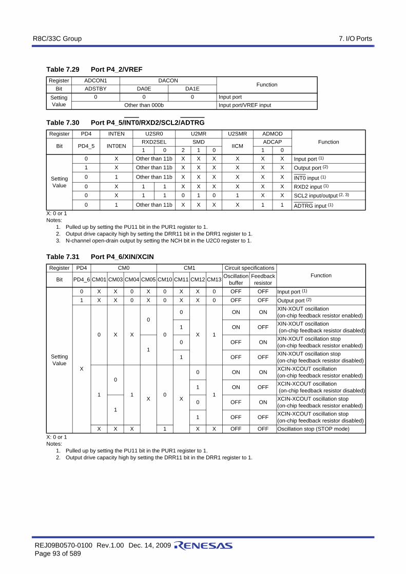
R8C/33C Group 7. I/O Ports
REJ09B0570-0100 Rev.1.00 Dec. 14, 2009Page 93 of 589
X: 0 or 1Notes:
1. Pulled up by setting the PU11 bit in the PUR1 register to 1.2. Output drive capacity high by setting the DRR11 bit in the DRR1 register to 1.3. N-channel open-drain output by setting the NCH bit in the U2C0 register to 1.
X: 0 or 1Notes:
1. Pulled up by setting the PU11 bit in the PUR1 register to 1.2. Output drive capacity high by setting the DRR11 bit in the DRR1 register to 1.
Table 7.29 Port P4_2/VREFRegister ADCON1 DACON
FunctionBit ADSTBY DA0E DA1E
Setting Value
0 0 0 Input portOther than 000b Input port/VREF input
Table 7.30 Port P4_5/INT0/RXD2/SCL2/ADTRGRegister PD4 INTEN U2SR0 U2MR U2SMR ADMOD
FunctionBit PD4_5 INT0EN
RXD2SEL SMDIICM
ADCAP1 0 2 1 0 1 0
Setting Value
0 X Other than 11b X X X X X X Input port (1)
1 X Other than 11b X X X X X X Output port (2)
0 1 Other than 11b X X X X X X INT0 input (1)
0 X 1 1 X X X X X X RXD2 input (1)
0 X 1 1 0 1 0 1 X X SCL2 input/output (2, 3)
0 1 Other than 11b X X X X 1 1 ADTRG input (1)
Table 7.31 Port P4_6/XIN/XCINRegister PD4 CM0 CM1 Circuit specifications
FunctionBit PD4_6 CM01 CM03 CM04 CM05 CM10 CM11 CM12 CM13 Oscillation
bufferFeedback resistor
Setting Value
0 X X 0 X 0 X X 0 OFF OFF Input port (1)
1 X X 0 X 0 X X 0 OFF OFF Output port (2)
X
0 X X
0
0
0
X 1
ON ON XIN-XOUT oscillation (on-chip feedback resistor enabled)
1 ON OFF XIN-XOUT oscillation (on-chip feedback resistor disabled)
10 OFF ON XIN-XOUT oscillation stop
(on-chip feedback resistor enabled)
1 OFF OFF XIN-XOUT oscillation stop (on-chip feedback resistor disabled)
1
0
1X
0X
0
1
ON ON XCIN-XCOUT oscillation (on-chip feedback resistor enabled)
1 ON OFF XCIN-XCOUT oscillation (on-chip feedback resistor disabled)
10 OFF ON XCIN-XCOUT oscillation stop
(on-chip feedback resistor enabled)
1 OFF OFF XCIN-XCOUT oscillation stop (on-chip feedback resistor disabled)
X X X 1 X X OFF OFF Oscillation stop (STOP mode)

R8C/33C Group 7. I/O Ports
REJ09B0570-0100 Rev.1.00 Dec. 14, 2009Page 94 of 589
X: 0 or 1Note:
1. Pulled up by setting the PU11 bit in the PUR1 register to 1.2. Output drive capacity high by setting the DRR11 bit in the DRR1 register to 1.3. Since the XCIN-XCOUT oscillation buffer operates with internal step-down power, the XCOUT output level cannot be used as
the CMOS level signal directly.
Table 7.32 Port P4_7/XOUT/XCOUTRegister PD4 CM0 CM1 Circuit specifications
FunctionBit PD4_7 CM01 CM03 CM04 CM05 CM10 CM11 CM12 CM13 Oscillation
bufferFeedback resistor
Setting Value
0 X X 0 X 0 X X 0 OFF OFF Input port (1)
1 X X 0 X 0 X X 0 OFF OFF Output port (2)
X
0 X X
0
0
0
X 1
ON ON XIN-XOUT oscillation (on-chip feedback resistor enabled)
1 ON OFF XIN-XOUT oscillation(on-chip feedback resistor disabled)
10 OFF ON XIN-XOUT oscillation stop
(on-chip feedback resistor enabled)
1 OFF OFF XIN-XOUT oscillation stop (on-chip feedback resistor disabled)
1
0
1X
0X
0
1
ON ONXCIN-XCOUT oscillation (on-chip feedback resistor enabled) (3)
1 ON OFFXCIN-XCOUT oscillation(on-chip feedback resistor disabled) (3)
10 OFF ON XCIN-XCOUT oscillation stop
(on-chip feedback resistor enabled)
1 OFF OFF XCIN-XCOUT oscillation stop (on-chip feedback resistor disabled)
X X X 1 X X OFF OFF Oscillation stop (STOP mode)

R8C/33C Group 7. I/O Ports
REJ09B0570-0100 Rev.1.00 Dec. 14, 2009Page 95 of 589
X: 0 or 1
X: 0 or 1
X: 0 or 1
X: 0 or 1
Table 7.33 TRBO Pin SettingRegister TRBIOC TRBMR
FunctionBit TOCNT TMOD1 TMOD0
Setting Value
0 0 1 Programmable waveform generation mode (pulse output)1 0 1 Programmable waveform generation mode (programmable output)0 1 0 Programmable one-shot generation mode0 1 1 Programmable wait one-shot generation mode
Table 7.34 TRCIOA Pin SettingRegister TRCOER TRCMR TRCIOR0 TRCCR2
FunctionBit EA PWM2 IOA2 IOA1 IOA0 TCEG1 TCEG0
Setting Value
0 1 00 1
X X Timer waveform output (output compare function)1 X
01 1 X X X X Timer mode (input capture function)
1
1 0 X X X0 1
PWM2 mode TRCTRG input1 X
Table 7.35 TRCIOB Pin SettingRegister TRCOER TRCMR TRCIOR0
FunctionBit EB PWM2 PWMB IOB2 IOB1 IOB0
Setting Value
0 0 X X X X PWM2 mode waveform output0 1 1 X X X PWM mode waveform output
0 1 0 00 1 Timer waveform output (output compare
function)1 X0
1 0 1 X X Timer mode (input capture function)1
Table 7.36 TRCIOC Pin SettingRegister TRCOER TRCMR TRCIOR1
FunctionBit EC PWM2 PWMC IOC2 IOC1 IOC0
Setting Value
0 1 1 X X X PWM mode waveform output
0 1 0 00 1 Timer waveform output (output compare
function)1 X0
1 0 1 X X Timer mode (input capture function)1
Table 7.37 TRCIOD Pin SettingRegister TRCOER TRCMR TRCIOR1
FunctionBit ED PWM2 PWMD IOD2 IOD1 IOD0
Setting Value
0 1 1 X X X PWM mode waveform output
0 1 0 00 1 Timer waveform output (output compare
function)1 X0
1 0 1 X X Timer mode (input capture function)1

R8C/33C Group 7. I/O Ports
REJ09B0570-0100 Rev.1.00 Dec. 14, 2009Page 96 of 589
7.6 Unassigned Pin HandlingTable 7.38 lists Unassigned Pin Handling. Figure 7.12 shows the Unassigned Pin Handling.
Notes:1. If these ports are set to output mode and left open, they remain in input mode until they are switched
to output mode by a program. The voltage level of these pins may be undefined and the powercurrent may increase while the ports remain in input mode.The content of the direction registers may change due to noise or program runaway caused bynoise. In order to enhance program reliability, the program should periodically repeat the setting ofthe direction registers.
2. Connect these unassigned pins to the MCU using the shortest wire length (2 cm or less) possible.3. When the power-on reset function is in use.
Figure 7.12 Unassigned Pin Handling
Table 7.38 Unassigned Pin HandlingPin Name Connection
Ports P0, P1, P2_0 to P2_2, P3_1, P3_3 to P3_5, P3_7, P4_5 to P4_7
• After setting to input mode, connect each pin to VSS via a resistor (pull-down) or connect each pin to VCC via a resistor (pull-up). (2)
• After setting to output mode, leave these pins open. (1, 2)
Port P4_2/VREF Connect to VCCRESET (3) Connect to VCC via a pull-up resistor (2)
Note: 1. When the power-on reset function is in use.
MCU
Port P0, P1,P2_0 to P2_2,
P3_1, P3_3 to P3_5,P3_7, P4_5 to P4_7
(Input mode )::
(Input mode)
(Output mode)
::
Open
RESET (1)
Port P4_2/VREF

R8C/33C Group 8. Bus
REJ09B0570-0100 Rev.1.00 Dec. 14, 2009Page 97 of 589
8. BusThe bus cycles differ when accessing ROM, RAM, DTC vector area, DTC control data and when accessing SFR.Table 8.1 lists Bus Cycles by Access Area of R8C/33C Group.ROM, RAM, DTC vector area, DTC control data and SFR are connected to the CPU by an 8-bit bus. When accessingin word (16-bit) units, these areas are accessed twice in 8-bit units.Table 8.2 shows Access Units and Bus Operations.
Table 8.2 Access Units and Bus Operations
Table 8.1 Bus Cycles by Access Area of R8C/33C GroupAccess Area Bus Cycle
SFR/Data flash 2 cycles of CPU clockProgram ROM/RAM 1 cycle of CPU clock
Area SFR, Data flash
Even addressByte access
ROM (program ROM), RAM,DTC vector area, DTC control data
Odd addressByte access
Even addressWord access
Odd addressWord access
CPU clock
Data Data Data
Even EvenAddress
CPU clock
Data
Address
CPU clock
Data
Address
CPU clock
Data
Address
CPU clock
Data
Address
CPU clock
Data
Address
CPU clock
Data
Address
CPU clock
Data
Address
Data Data
Odd Odd
Data
Even Even + 1
Data
Data
Odd Odd + 1
Data
Data
Even Even + 1
Data
Data
Odd Odd + 1
Data

R8C/33C Group 8. Bus
REJ09B0570-0100 Rev.1.00 Dec. 14, 2009Page 98 of 589
However, only the following SFRs are connected with the 16-bit bus:
Interrupts: Each interrupt control registerTimer RC: Registers TRC, TRCGRA, TRCGRB, TRCGRC, and TRCGRDSSU: Registers SSTDR, SSTDRH, SSRDR, and SSRDRHUART2: Registers U2MR, U2BRG, U2TB, U2C0, U2C1, U2RB, U2SMR5, U2SMR4, U2SMR3, U2SMR2,
and U2SMRA/D converter: Registers AD0, AD1, AD2, AD3, AD4, AD5, AD6, AD7, ADMOD, ADINSEL, ADCON0,
and ADCON1D/A converter: Registers DA0 and DA1Address match interrupt: Registers RMAD0, AIER0, RMAD1, and AIER1Therefore, they are accessed once in 16-bit units. The bus operation is the same as “Area: SFR, Data flash, Evenaddress Byte Access” in Table 8.2 Access Units and Bus Operations, and 16-bit data is accessed at a time.

R8C/33C Group 9. Clock Generation Circuit
REJ09B0570-0100 Rev.1.00 Dec. 14, 2009Page 99 of 589
9. Clock Generation CircuitThe following five circuits are incorporated in the clock generation circuit:• XIN clock oscillation circuit• XCIN clock oscillation circuit• Low-speed on-chip oscillator• High-speed on-chip oscillator• Low-speed on-chip oscillator for watchdog timer
9.1 OverviewTable 9.1 lists the Specification Overview of Clock Generation Circuit. Figure 9.1 shows a Clock GenerationCircuit (With XIN and XCIN Pins Shared). Figure 9.2 shows a Peripheral Function Clock and Figure 9.3 shows aProcedure for Reducing Internal Power Consumption Using VCA20 bit.
Notes:1. These pins can be used as P4_6 or P4_7 when using the on-chip oscillator clock as the CPU clock while the
XIN clock oscillation circuit and the XCIN clock oscillation circuit are not used.2. To input an external clock, set the CM05 bit in the CM0 register to 1 (XIN clock stops), the CM11 bit in the CM1
register to 1 (internal feedback resistor disabled), and the CM13 bit to 1 (XIN-XOUT pin).3. The clock frequency is automatically set to up to 20 MHz by a divider when using the high-speed on-chip
oscillator as the CPU clock source.4. This applies when the CSPROINI bit in the OFS register is set to 1 (count source protection mode disabled after reset).5. This applies when the CSPROINI bit in the OFS register is set to 0 (count source protection mode enabled after reset).
Table 9.1 Specification Overview of Clock Generation Circuit
Item XIN Clock Oscillation Circuit
XCIN Clock Oscillation Circuit
On-Chip Oscillator Low-Speed On-Chip Oscillator
for Watchdog TimerHigh-Speed
On-Chip OscillatorLow-Speed
On-Chip OscillatorApplications • CPU clock
source• Peripheral
function clock source
• CPU clock source
• Peripheral function clock source
• CPU clock source
• Peripheral function clock source
• CPU and peripheral function clock source when XIN clock stops oscillating
• CPU clock source
• Peripheral function clock source
• CPU and peripheral function clock source when XIN clock stops oscillating
• Watchdog timer clock source
Clock frequency 0 to 20 MHz 32.768 kHz Approx. 40 MHz (3) Approx. 125 kHz Approx. 125 kHzConnectable oscillator
• Ceramic resonator
• Crystal oscillator
• Crystal oscillator
− − −
Oscillator connect pins
XIN, XOUT (1) XCIN, XCOUT (1) − (1) − (1) −
Oscillation stop, restart function
Usable Usable Usable Usable Usable
Oscillator status after reset
Stop Stop Stop Oscillate Stop (4)
Oscillate (5)
Others Externally generated clock can be input (2)
• Externally generated clock can be input
• On-chip feedback resistor Rf (connected/ not connected selectable)
− − −
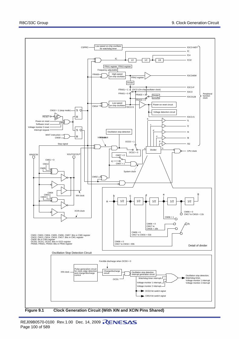
R8C/33C Group 9. Clock Generation Circuit
REJ09B0570-0100 Rev.1.00 Dec. 14, 2009Page 100 of 589
Figure 9.1 Clock Generation Circuit (With XIN and XCIN Pins Shared)
S Q
R
1/2 1/2 1/2 1/2 1/2
Charge/dischargecircuit Oscillation stop detection
Interrupt generation circuit
S Q
R
High-speedon-chip oscillator
FRA01 = 1
FRA01 = 0
CM14
b
c
d
e
Divider
XIN clockWAIT instruction
RESET
CM10 = 1 (stop mode)
a
dc
h
b
CM06 = 0CM17 to CM16 = 11b
CM06 = 1
CM06 = 0CM17 toCM16 = 10b
CM06 = 0CM17 to CM16 = 01b
CM06 = 0CM17 to CM16 = 00b Detail of divider
Oscillation Stop Detection Circuit
Pulse generation circuitfor clock edge detectionand charge/dischargecontrol
XIN clock
Forcible discharge when OCD0 = 0
OCD1
OCD2 bit switch signal
CM14 bit switch signal
Oscillation stop detection,Watchdog timer,Voltage monitor 1 interrupt,Voltage monitor 2 interrupt
CM02, CM03, CM04, CM05, CM06, CM07: Bits in CM0 registerCM10, CM13, CM14, CM16, CM17: Bits in CM1 registerCM30: Bit in CM3 registerOCD0, OCD1, OCD2: Bits in OCD registerFRA00, FRA01, FRA03: Bits in FRA0 register
e g
FRA2 register
fOCO (On-chip oscillator clock)
fOCO-S
g
h
Low-speedon-chip oscillator
Frequency adjustable
Divider
fC
Power-on reset circuit
Voltage detection circuit
Divider(1/128)
Power-on resetSoftware reset
Voltage monitor 0 reset
1/81/2
CPU clock
f1
f2
f4
f8
f32
fOCO40M
fC4
fC32
fOCO-F
fOCO
fOCO128
fOCO-S
Peripheralfunctionclock
1/2
fC
fOCO-WDTLow-speed on-chip oscillatorfor watchdog timerCSPRO
CM30
XIN clock
XOUT/XCOUTXIN/XCIN
CM04
XCIN clock
CM01 = 0
CM13
CM05
Stop signal
CM01CM03
Watchdog timer interrupt
Voltage monitor 1 interrupt
Voltage monitor 2 interrupt
FRA03 = 1
FRA03 = 0
FRA00
FRA1 register, FRA3 register
a
OCD2 = 0
OCD2 = 1
Oscillation stop detection
XIN clock
System clock
CM07 = 0
CM07 = 1fC
CM02
Interrupt request

R8C/33C Group 9. Clock Generation Circuit
REJ09B0570-0100 Rev.1.00 Dec. 14, 2009Page 101 of 589
Figure 9.2 Peripheral Function Clock
UART0A/D converterTimer RBTimer RAINT0SSU /
I2C bus
Watchdogtimer
UART1Timer RE
CPU clock
f1
f2
f4
f8
f32
fOCO40M
fOCO-F
fC4
fC32
fOCO128
Timer RC UART2
fOCO-WDT
fOCO
CPU
fC

R8C/33C Group 9. Clock Generation Circuit
REJ09B0570-0100 Rev.1.00 Dec. 14, 2009Page 102 of 589
9.2 Registers
9.2.1 System Clock Control Register 0 (CM0)
Notes:1. The CM05 bit stops the XIN clock when the high-speed on-chip oscillator mode or low-speed on-chip oscillator
mode is selected. This bit cannot be used to detect whether the XIN clock has stopped. To stop the XIN clock, setthe bits in the following order:(a) Set bits OCD1 to OCD0 in the OCD register to 00b.(b) Set the OCD2 bit to 1 (on-chip oscillator clock selected).
2. During external clock input, only the clock oscillation buffer stops and clock input is acknowledged.3. Only when the CM05 bit is set to 1 (XIN clock stops) and the CM13 bit in the CM1 register is set to 0 (P4_6 and
P4_7), P4_6 and P4_7 can be used as I/O ports.4. When the MCU enters stop mode, the CM06 bit is set to 1 (divide-by-8 mode).5. The CM04 bit can be set to 1 by a program but cannot be set to 0.6. To use the XCIN clock, set the CM04 bit to 1.7. Set the CM07 bit to 1 (XCIN clock) from 0 after setting the CM04 bit to 1 (XCIN-XCOUT pin) and allowing XCIN
clock oscillation to stabilize.
Set the PRC0 bit in the PRCR register to 1 (write enabled) before rewriting the CM0 register.
Address 0006hBit b7 b6 b5 b4 b3 b2 b1 b0
Symbol CM07 CM06 CM05 CM04 CM03 CM02 CM01 —After Reset 0 0 1 0 1 0 0 0
Bit Symbol Bit Name Function R/Wb0 — Reserved bit Set to 0. R/Wb1 CM01 XIN-XCIN switch bit 0: P4_6 and P4_7 set as XIN-XOUT pin
1: P4_6 and P4_7 set as XCIN-XCOUT pinR/W
b2 CM02 Wait mode peripheral function clock stop bit
0: Peripheral function clock does not stop in wait mode1: Peripheral function clock stops in wait mode
R/W
b3 CM03 XCIN clock stop bit 0: XCIN clock oscillates1: XCIN clock stops
R/W
b4 CM04 Port/XCIN-XCOUT switch bit (5) 0: I/O ports P4_6 and P4_71: XCIN-XCOUT pin (6)
R/W
b5 CM05 XIN clock (XIN-XOUT) stop bit (1, 3) 0: XIN clock oscillates1: XIN clock stops (2)
R/W
b6 CM06 CPU clock division select bit 0 (4) 0: Bits CM16 and CM17 in CM1 register enabled1: Divide-by-8 mode
R/W
b7 CM07 XIN, XCIN clock select bit (7) 0: XIN clock1: XCIN clock
R/W

R8C/33C Group 9. Clock Generation Circuit
REJ09B0570-0100 Rev.1.00 Dec. 14, 2009Page 103 of 589
9.2.2 System Clock Control Register 1 (CM1)
Notes:1. When the CM06 bit is set to 0 (bits CM16 and CM17 enabled), bits CM16 and CM17 are enabled.2. If the CM10 bit is set to 1 (stop mode), the on-chip feedback resistor is disabled.3. When the OCD2 bit is set to 0 (XIN clock selected), the CM14 bit can be set to 1 (low-speed on-chip oscillator
off). When the OCD2 bit is set to 1 (on-chip oscillator clock selected), the CM14 bit is set to 0 (low-speed on-chiposcillator on). It remains unchanged even if 1 is written to it.
4. To use the voltage monitor 1 interrupt or voltage monitor 2 interrupt (when the digital filter is used), set the CM14bit to 0 (low-speed on-chip oscillator on).
5. Once the CM13 bit is set to 1 by a program, it cannot be set to 0.6. Do not set the CM10 bit to 1 (stop mode) when the VCA20 bit in the VCA2 register to 1 (low consumption
enabled).
Set the PRC0 bit in the PRCR register to 1 (write enabled) before rewriting the CM1 register.
Address 0007hBit b7 b6 b5 b4 b3 b2 b1 b0
Symbol CM17 CM16 — CM14 CM13 CM12 CM11 CM10After Reset 0 0 1 0 0 0 0 0
Bit Symbol Bit Name Function R/Wb0 CM10 All clock stop control bit (2, 6) 0: Clock oscillates
1: All clocks stop (stop mode)R/W
b1 CM11 XIN-XOUT on-chip feedback resistor select bit
0: On-chip feedback resistor enabled1: On-chip feedback resistor disabled
R/W
b2 CM12 XCIN-XCOUT on-chip feedback resistor select bit
0: On-chip feedback resistor enabled1: On-chip feedback resistor disabled
R/W
b3 CM13 Port/XIN-XOUT switch bit (5) 0: I/O ports P4_6 and P4_71: XIN-XOUT pin
R/W
b4 CM14 Low-speed on-chip oscillator stop bit (3, 4)
0: Low-speed on-chip oscillator on1: Low-speed on-chip oscillator off
R/W
b5 — Reserved bit Set to 1. R/Wb6 CM16 CPU clock division select bit 1 (1) b7 b6
0 0: No division mode 0 1: Divide-by-2 mode 1 0: Divide-by-4 mode 1 1: Divide-by-16 mode
R/Wb7 CM17 R/W

R8C/33C Group 9. Clock Generation Circuit
REJ09B0570-0100 Rev.1.00 Dec. 14, 2009Page 104 of 589
9.2.3 System Clock Control Register 3 (CM3)
Notes:1. When the MCU exits wait mode by a peripheral function interrupt, the CM30 bit is set to 0 (other than wait mode).2. Set the CM35 bit to 0 in stop mode. When the MCU enters wait mode, if the CM35 bit is set to 1 (no division), the
CM06 bit in the CM0 register is set to 0 (bits CM16 and CM17 enabled) and bits CM17 and CM16 in the CM1register is set to 00b (no division mode).
3. When bits CM37 and CM36 are set to 10b (high-speed on-chip oscillator clock selected), the following will be setwhen the MCU exits wait mode or stop mode.• OCD2 bit in OCD register = 1 (on-chip oscillator selected)• FRA00 bit in FRA0 register = 1 (high-speed on-chip oscillator on)• FRA01 bit in FRA0 register = 1 (high-speed on-chip oscillator selected)
4. When bits CM37 and CM36 are set to 11b (XIN clock selected), the following will be set when the MCU exits waitmode or stop mode.• OM05 bit in OM0 register = 1 (XIN clock oscillates)• OM13 bit in OM1 register = 1 (XIN-XOUT pin)• OCD2 bit in OCD register = 0 (XIN clock selected)When the MCU enters wait mode while the CM05 bit in the CM0 register is 1 (XIN clock stops), if the XIN clock isselected as the CPU clock when exiting wait mode, set the CM06 bit to 1 (divide-by-8 mode) and the CM35 bit to0.However, if an externally generated clock is used as the XIN clock, do not set bits CM37 to CM36 to 11b (XINclock selected).
Set the PRC0 bit in the PRCR register to 1 (write enabled) before rewriting the CM3 register.
CM30 bit (Wait Control Bit)When the CM30 bit is set to 1 (MCU enters wait mode), the CPU clock stops (wait mode). Since the XIN clock,XCIN clock, and the on-chip oscillator clock do not stop, the peripheral functions using these clocks continueoperating. To set the CM30 bit to 1, set the I flag to 0 (maskable interrupt disabled).The MCU exits wait mode by a reset or peripheral function interrupt. When the MCU exits wait mode by aperipheral function interrupt, it resumes executing the instruction immediately after the instruction to set theCM30 bit to 1. When the MCU enters wait mode with the WAIT instruction, make sure to set the I flag to 1 (maskable interruptenabled). With this setting, interrupt handling is performed by the CPU when the MCU exits wait mode.
Address 0009hBit b7 b6 b5 b4 b3 b2 b1 b0
Symbol CM37 CM36 CM35 — — — — CM30After Reset 0 0 0 0 0 0 0 0
Bit Symbol Bit Name Function R/Wb0 CM30 Wait control bit (1) 0: Other than wait mode
1: MCU enters wait modeR/W
b1 — Nothing is assigned. If necessary, set to 0. When read, the content is 0. —b2 —b3 — Reserved bits Set to 0. R/Wb4 —b5 CM35 CPU clock division when exiting
wait mode select bit (2)0: Following settings are enabled:
CM06 bit in CM0 registerBits CM16 and CM17 in CM1 register
1: No division
R/W
b6 CM36 System clock when exiting wait mode or stop mode select bit
b7 b6 0 0: MCU exits with the CPU clock immediately
before entering wait or stop mode. 0 1: Do not set. 1 0: High-speed on-chip oscillator clock selected (3)
1 1: XIN clock selected (4)
R/Wb7 CM37 R/W

R8C/33C Group 9. Clock Generation Circuit
REJ09B0570-0100 Rev.1.00 Dec. 14, 2009Page 105 of 589
9.2.4 Oscillation Stop Detection Register (OCD)
Notes:1. Set bits OCD1 to OCD0 to 00b before the MCU enters stop mode, high-speed on-chip oscillator mode, or low-
speed on-chip oscillator mode (XIN clock stops).2. If the OCD2 bit is set to 1 (on-chip oscillator clock selected), the CM14 bit is set to 0 (low-speed on-chip oscillator
on).3. The OCD2 bit is automatically set to 1 (on-chip oscillator clock selected) if XIN clock oscillation stop is detected
while bits OCD1 to OCD0 are set to 11b. If the OCD3 bit is set to 1 (XIN clock stops), the OCD2 bit remainsunchanged even when set to 0 (XIN clock selected).
4. The OCD3 bit is enabled when the OCD0 bit is set to 1 (oscillation stop detection function enabled).5. The OCD3 bit remains 0 (XIN clock oscillates) if bits OCD1 to OCD0 are set to 00b.6. Refer to Figure 9.10 Procedure for Switching Clock Source from Low-Speed On-Chip Oscillator to XIN
Clock for the switching procedure when the XIN clock re-oscillates after detecting oscillation stop.
Set the PRC0 bit in the PRCR register to 1 (write enabled) before rewriting the OCD register.
9.2.5 High-Speed On-Chip Oscillator Control Register 7 (FRA7)
Address 000ChBit b7 b6 b5 b4 b3 b2 b1 b0
Symbol — — — — OCD3 OCD2 OCD1 OCD0After Reset 0 0 0 0 0 1 0 0
Bit Symbol Bit Name Function R/Wb0 OCD0 Oscillation stop detection enable bit (6) 0: Oscillation stop detection function disabled (1)
1: Oscillation stop detection function enabledR/W
b1 OCD1 Oscillation stop detection interrupt enable bit
0: Disabled (1)
1: EnabledR/W
b2 OCD2 System clock select bit (3) 0: XIN clock selected (6)
1: On-chip oscillator clock selected (2)R/W
b3 OCD3 Clock monitor bit (4, 5) 0: XIN clock oscillates1: XIN clock stops
R
b4 — Reserved bits Set to 0. R/Wb5 —b6 —b7 —
Address 0015hBit b7 b6 b5 b4 b3 b2 b1 b0
Symbol — — — — — — — —After Reset When shipping
Bit Function R/Wb7-b0 32 MHz frequency correction data is stored.
The frequency can be adjusted by transferring this value to the FRA3 register and by transferring the correction value in the FRA6 register to the FRA1 register.
R

R8C/33C Group 9. Clock Generation Circuit
REJ09B0570-0100 Rev.1.00 Dec. 14, 2009Page 106 of 589
9.2.6 High-Speed On-Chip Oscillator Control Register 0 (FRA0)
Notes:1. Change the FRA01 bit in the following conditions.
• FRA00 = 1 (high-speed on-chip oscillator on)• The CM14 bit in the CM1 register = 0 (low-speed on-chip oscillator on)• Bits FRA22 to FRA20 in the FRA2 register:
All division mode can be set when VCC = 2.7 V to 5.5 V 000b to 111b Divide ratio of 8 or more when VCC = 1.8 V to 5.5 V 110b to 111b (divide-by-8 or more)
2. When setting the FRA01 bit to 0 (low-speed on-chip oscillator selected), do not set the FRA00 bit to 0 (high-speed on-chip oscillator off) at the same time. Set the FRA00 bit to 0 after setting the FRA01 bit to 0.
Set the PRC0 bit in the PRCR register to 1 (write enabled) before rewriting the FRA0 register.
9.2.7 High-Speed On-Chip Oscillator Control Register 1 (FRA1)
Set the PRC0 bit in the PRCR register to 1 (write enabled) before rewriting the FRA1 register.Also, rewrite the FRA1 register when the FRA00 bit in the FRA0 register is set 0 (high-speed on-chip oscillatoroff).
Address 0023hBit b7 b6 b5 b4 b3 b2 b1 b0
Symbol — — — — FRA03 — FRA01 FRA00After Reset 0 0 0 0 0 0 0 0
Bit Symbol Bit Name Function R/Wb0 FRA00 High-speed on-chip oscillator enable bit 0: High-speed on-chip oscillator off
1: HIgh-speed on-chip oscillator onR/W
b1 FRA01 High-speed on-chip oscillator select bit (1) 0: Low-speed on-chip oscillator selected (2)
1: High-speed on-chip oscillator selectedR/W
b2 — Reserved bits Set to 0. R/Wb3 FRA03 fOCO128 clock select bit 0: fOCO-S divided by 128 selected
1: fOCO-F divided by 128 selectedR/W
b4 — Nothing is assigned. If necessary, set to 0. When read, the content is 0. —b5 —b6 —b7 —
Address 0024hBit b7 b6 b5 b4 b3 b2 b1 b0
Symbol — — — — — — — —After Reset When shipping
Bit Function R/Wb7-b0 The frequency of the high-speed on-chip oscillator can be adjusted by setting as follows:
40 MHz: FRA1 = value after reset, FRA3 = value after reset36.864 MHz: Transfer the value in the FRA4 register to the FRA1 register and the value in
the FRA5 register to the FRA3 register.32 MHz: Transfer the value in the FRA6 register to the FRA1 register and the value in
the FRA7 register to the FRA3 register.
R/W

R8C/33C Group 9. Clock Generation Circuit
REJ09B0570-0100 Rev.1.00 Dec. 14, 2009Page 107 of 589
9.2.8 High-Speed On-Chip Oscillator Control Register 2 (FRA2)
Set the PRC0 bit in the PRCR register to 1 (write enabled) before rewriting the FRA2 register.
9.2.9 Clock Prescaler Reset Flag (CPSRF)
Address 0025hBit b7 b6 b5 b4 b3 b2 b1 b0
Symbol — — — — — FRA22 FRA21 FRA20After Reset 0 0 0 0 0 0 0 0
Bit Symbol Bit Name Function R/Wb0 FRA20 High-speed on-chip oscillator frequency
switching bitDivision selectionThese bits select the division ratio for the high-speed on-chip oscillator clock.b2 b1 b0 0 0 0: Divide-by-2 mode 0 0 1: Divide-by-3 mode 0 1 0: Divide-by-4 mode 0 1 1: Divide-by-5 mode 1 0 0: Divide-by-6 mode 1 0 1: Divide-by-7 mode 1 1 0: Divide-by-8 mode 1 1 1: Divide-by-9 mode
R/Wb1 FRA21 R/Wb2 FRA22 R/W
b3 — Reserved bits Set to 0. R/Wb4 —b5 —b6 —b7 —
Address 0028hBit b7 b6 b5 b4 b3 b2 b1 b0
Symbol CPSR — — — — — — —After Reset 0 0 0 0 0 0 0 0
Bit Symbol Bit Name Function R/Wb0 — Reserved bits Set to 0. R/Wb1 —b2 —b3 —b4 —b5 —b6 —b7 CPSR Clock prescaler reset flag Setting this bit to 1 initializes the clock prescaler.
(When read, the content is 0.)R/W

R8C/33C Group 9. Clock Generation Circuit
REJ09B0570-0100 Rev.1.00 Dec. 14, 2009Page 108 of 589
9.2.10 High-Speed On-Chip Oscillator Control Register 4 (FRA4)
9.2.11 High-Speed On-Chip Oscillator Control Register 5 (FRA5)
9.2.12 High-Speed On-Chip Oscillator Control Register 6 (FRA6)
9.2.13 High-Speed On-Chip Oscillator Control Register 3 (FRA3)
Set the PRC0 bit in the PRCR register to 1 (write enabled) before rewriting the FRA3 register.Also, rewrite the FRA3 register when the FRA00 bit in the FRA0 register is set 0 (high-speed on-chip oscillatoroff).
Address 0029hBit b7 b6 b5 b4 b3 b2 b1 b0
Symbol — — — — — — — —After Reset When shipping
Bit Function R/Wb7-b0 36.864 MHz frequency correction data is stored.
The frequency can be adjusted by transferring this value to the FRA1 register and by transferring the correction value in the FRA5 register to the FRA3 register.
R
Address 002AhBit b7 b6 b5 b4 b3 b2 b1 b0
Symbol — — — — — — — —After Reset When shipping
Bit Function R/Wb7-b0 36.864 MHz frequency correction data is stored.
The frequency can be adjusted by transferring this value to the FRA3 register and by transferring the correction value in the FRA4 register to the FRA1 register.
R
Address 002BhBit b7 b6 b5 b4 b3 b2 b1 b0
Symbol — — — — — — — —After Reset When shipping
Bit Function R/Wb7-b0 32 MHz frequency correction data is stored.
The frequency can be adjusted by transferring this value to the FRA1 register and by transferring the correction value in the FRA7 register to the FRA3 register.
R
Address 002FhBit b7 b6 b5 b4 b3 b2 b1 b0
Symbol — — — — — — — —After Reset When shipping
Bit Function R/Wb7-b0 The frequency of the high-speed on-chip oscillator can be adjusted by setting as follows:
40 MHz: FRA1 = value after reset, FRA3 = value after reset36.864 MHz: Transfer the value in the FRA4 register to the FRA1 register and the value in
the FRA5 register to the FRA3 register.32 MHz: Transfer the value in the FRA6 register to the FRA1 register and the value in
the FRA7 register to the FRA3 register.
R/W

R8C/33C Group 9. Clock Generation Circuit
REJ09B0570-0100 Rev.1.00 Dec. 14, 2009Page 109 of 589
9.2.14 Voltage Detect Register 2 (VCA2)
Notes:1. Use the VCA20 bit only when the MCU enters wait mode. To set the VCA20 bit, follow the procedure shown in
Figure 9.3 Procedure for Reducing Internal Power Consumption Using VCA20 bit. 2. When the VCA20 bit is set to 1 (low consumption enabled), do not set the CM10 bit in the CM1 register to 1 (stop
mode).3. When writing to the VCA25 bit, set a value after reset.4. To use the voltage detection 1 interrupt or the VW1C3 bit in the VW1C register, set the VCA26 bit to 1.
After the VCA26 bit is set to 1 from 0, allow td(E-A) to elapse before the voltage detection 1 circuit startsoperation.
5. To use the voltage detection 2 interrupt or the VCA13 bit in the VCA1 register, set the VCA27 bit to 1.After the VCA27 bit is set to 1 from 0, allow td(E-A) to elapse before the voltage detection 2 circuit startsoperation.
Set the PRC3 bit in the PRCR register to 1 (write enabled) before rewriting the VCA2 register.
Address 0034hBit b7 b6 b5 b4 b3 b2 b1 b0
Symbol VCA27 VCA26 VCA25 — — — — VCA20After Reset 0 0 0 0 0 0 0 0
The above applies when the LVDAS bit in the OFS register is set to 1.After Reset 0 0 1 0 0 0 0 0
The above applies when the LVDAS bit in the OFS register is set to 0.
Bit Symbol Bit Name Function R/Wb0 VCA20 Internal power low consumption
enable bit (1)0: Low consumption disabled1: Low consumption enabled (2)
R/W
b1 — Reserved bits Set to 0. R/Wb2 —b3 —b4 —b5 VCA25 Voltage detection 0 enable bit (3) 0: Voltage detection 0 circuit disabled
1: Voltage detection 0 circuit enabledR/W
b6 VCA26 Voltage detection 1 enable bit (4) 0: Voltage detection 1 circuit disabled1: Voltage detection 1 circuit enabled
R/W
b7 VCA27 Voltage detection 2 enable bit (5) 0: Voltage detection 2 circuit disabled1: Voltage detection 2 circuit enabled
R/W

R8C/33C Group 9. Clock Generation Circuit
REJ09B0570-0100 Rev.1.00 Dec. 14, 2009Page 110 of 589
Figure 9.3 Procedure for Reducing Internal Power Consumption Using VCA20 bit
Notes:1. Execute this routine to handle all interrupts generated in wait mode.
However, this does not apply if it is not necessary to start the high-speed clock or high-speed on-chip oscillator during the interrupt routine.2. Do not set the VCA20 bit to 0 with the instruction immediately after setting the VCA20 bit to 1. Also, do not do the opposite.3. When the VCA20 bit is set to 1, do not set the CM10 bit to 1 (stop mode).4. When the MCU enters wait mode, follow 9.7.2 Wait Mode.
Procedure for enabling reduced internalpower consumption using VCA20 bit
Enter low-speed clock mode orlow-speed on-chip oscillator mode
Stop XIN clock andhigh-speed on-chip oscillator clock
VCA20 ← 1(internal power low consumption enabled) (2, 3)
Enter wait mode (4)
VCA20 ← 0(internal power low consumption disabled) (2)
Start XIN clock orhigh-speed on-chip oscillator clock
(Wait until XIN clock or high-speed on-chiposcillator clock oscillation stabilizes)
Enter high-speed clock mode orhigh-speed on-chip oscillator mode
In interrupt routine
VCA20 ← 0(internal power low consumption disabled) (2)
(This is automatically set when exiting wait mode)
Start XIN clockor high-speed on-chip oscillator clock
Enter high-speed clock mode orhigh-speed on-chip oscillator mode
Enter low-speed clock mode orlow-speed on-chip oscillator mode
Exit wait mode by interrupt
Stop XIN clock andhigh-speed on-chip oscillator clock
VCA20 ← 1(internal power low consumption enabled) (2, 3)
Interrupt handling completed
Step (1)
Step (2)
Step (3)
Step (4)
Step (5)
Step (6)
Step (7)
Step (8)
Step (5)
Step (6)
Step (7)
Step (8)
(Wait until XIN clock or high-speed on-chiposcillator clock oscillation stabilizes)
Step (1)
Step (2)
Step (3)
If it is necessary to startthe high-speed clock orhigh-speed on-chip oscillatorduring the interrupt routine,execute steps (6) to (7)in the routine.
If the high-speed clock orhigh-speed on-chip oscillatorstarts during the interruptroutine, execute steps (1) to(3) at the end of the routine.
(Note 1)
Interrupt handling
VCA20: Bit in VCA2 register

R8C/33C Group 9. Clock Generation Circuit
REJ09B0570-0100 Rev.1.00 Dec. 14, 2009Page 111 of 589
The clocks generated by the clock generation circuits are described below.
9.3 XIN ClockThe XIN clock is supplied by the XIN clock oscillation circuit. This clock is used as the clock source for the CPUand peripheral function clocks. The XIN clock oscillation circuit is configured by connecting a resonator betweenpins XIN and XOUT. The XIN clock oscillation circuit includes an on-chip feedback resistor, which isdisconnected from the oscillation circuit in stop mode in order to reduce the amount of power consumed by thechip. The XIN clock oscillation circuit may also be configured by feeding an externally generated clock to theXOUT pin.Figure 9.4 shows Examples of XIN Clock Connection Circuit. During and after a reset, the XIN clock stops.After setting the CM13 bit in the CM1 register to 1 (XIN-XOUT pin), the XIN clock starts oscillating when theCM05 bit in the CM0 register is set to 0 (XIN clock oscillates). After the XIN clock oscillation stabilizes, the XINclock is used as the CPU clock source when the OCD2 bit in the OCD register is set to 0 (XIN clock selected).The power consumption can be reduced by setting the CM05 bit in the CM0 register to 1 (XIN clock stops) if theOCD2 bit is set to 1 (on-chip oscillator clock selected).When an externally generated clock is input to the XOUT pin, the XIN clock does not stop even if the CM05 bit isset to 1. If necessary, use an external circuit to stop the clock.In stop mode, all clocks including the XIN clock stop. Refer to 9.7 Power Control for details.
Figure 9.4 Examples of XIN Clock Connection Circuit
XIN XOUT
MCU(on-chip feedback resistor)
Rd (1)
COUTCIN
XIN XOUT
MCU(on-chip feedback resistor)
Externally generated clockVCC
VSS
Notes: 1. Insert a damping resistor if required. The resistance will vary depending on the oscillator and
the oscillation drive capacity settings. Use the values recommended by the oscillator manufacturer.If the oscillator manufacturer's datasheet specifies that a feedback resistor be added to the chipexternally, insert a feedback resistor between XIN and XOUT following the instructions.
2. Insert a damping resistor if required to prevent an overshoot from occurring.
Open
Ceramic resonator external circuit External clock input circuit
Rf (1)
• When CM05 bit in CM0 registeris set to 0 (XIN clock oscillates)and CM13 bit in CM1 register isset to 1 (XIN-XOUT pin)
• When CM05 bit in CM0 registeris set to 1 (XIN clock stops),CM11 bit in CM1 register is setto 1 (internal feedback resistordisabled), and the CM13 bit isset to 1 (XIN-XOUT pin)
(2)
R8C/33C Group 9. Clock Generation Circuit
REJ09B0570-0100 Rev.1.00 Dec. 14, 2009Page 112 of 589
9.4 On-Chip Oscillator ClockThe on-chip oscillator clock is supplied by the on-chip oscillator (high-speed on-chip oscillator or low-speed on-chip oscillator). This clock is selected by the FRA01 bit in the FRA0 register.
9.4.1 Low-Speed On-Chip Oscillator ClockThe clock generated by the low-speed on-chip oscillator is used as the clock source for the CPU clock,peripheral function clock, fOCO, fOCO-S, and fOCO128.After a reset, the on-chip oscillator clock generated by the low-speed on-chip oscillator divided by 1 (nodivision) is selected as the CPU clock.If the XIN clock stops oscillating when bits OCD1 to OCD0 in the OCD register are set to 11b, the low-speedon-chip oscillator automatically starts operating and supplies the necessary clock for the MCU.The frequency of the low-speed on-chip oscillator varies depending on the supply voltage and the operatingambient temperature. Application products must be designed with sufficient margin to allow for frequencychanges.
9.4.2 High-Speed On-Chip Oscillator ClockThe clock generated by the high-speed on-chip oscillator is used as the clock source for the CPU clock,peripheral function clock, fOCO, fOCO-F, fOCO40M, and fOCO128.To use the high-speed on-chip oscillator clock as the clock source for the CPU clock, peripheral clock, fOCO,and fOCO-F, set bits FRA20 to FRA22 in the FRA2 register as follows:•All division mode can be set when VCC = 2.7 V to 5.5 V 000b to 111b•Divide ratio of 8 or more when VCC = 1.8 V to 5.5 V 110b to 111b (divide by 8 or more)
After a reset, the on-chip oscillator clock generated by the high-speed on-chip oscillator stops. Oscillation isstarted by setting the FRA00 bit in the FRA0 register to 1 (high-speed on-chip oscillator on).
Frequency correction data is stored in registers FRA4 to FRA7.To adjust the frequency of the high-speed on-chip oscillator clock to 36.864 MHz, first transfer the correctionvalue in the FRA4 register to the FRA1 register and the correction value in the FRA5 register to the FRA3register before using the values. This enables the setting errors of bit rates such as 9600 bps and 38400 bps to be0% when the serial interface is used in UART mode (refer to Table 21.8 and Table 22.8 Bit Rate SettingExample in UART Mode).To adjust the frequency of the high-speed on-chip oscillator clock to 32 MHz, first transfer the correction valuein the FRA6 register to the FRA1 register and the correction value in the FRA7 register to the FRA3 registerbefore using the values.

R8C/33C Group 9. Clock Generation Circuit
REJ09B0570-0100 Rev.1.00 Dec. 14, 2009Page 113 of 589
9.5 XCIN ClockThe XCIN clock is supplied by the XCIN clock oscillation circuit. This clock is used as the clock source for theCPU and peripheral function clocks. The XCIN clock oscillation circuit is configured by connecting a resonatorbetween the XCIN and XCOUT pins. The XCIN clock oscillation circuit includes an on-chip a feedback resistor,which is disconnected from the oscillation circuit in stop mode in order to reduce the amount of power consumedby the chip. The XCIN clock oscillation circuit may also be configured by feeding an externally generated clock tothe XCIN pin.Figure 9.5 shows Examples of XCIN Clock Connection Circuits. During and after a reset, the XCIN clock stops.After setting the CM04 bit in the CM0 register to 1 (XCIN-XCOUT pin), the XCIN clock starts oscillating whenthe CM03 bit in the CM0 register is set to 0 (XCIN clock oscillates). After the XCIN clock oscillation stabilizes,the XCIN clock is used as the CPU clock source when the CM07 bit in the CM0 register is set to 1 (XCIN clock).To input an externally generated clock to the XCIN pin, also set the CM04 bit in the CM0 register to 1 (XCIN-XCOUT pin). Leave the XCOUT pin open at this time. This MCU has an on-chip feedback resistor, which can be disabled/enabled by the CM12 bit in the CM1 register.In stop mode, all clocks including the XCIN clock stop. Refer to 9.7 Power Control for details.
Figure 9.5 Examples of XCIN Clock Connection Circuits
XCIN XCOUT
MCU(on-chip feedback resistor)
Rd (1)
COUTCIN
XCIN XCOUT
MCU(on-chip feedback resistor)
Externally generated clock
VCC
VSS
Note: 1. Insert a damping resistor and feedback resistor if required. The resistance will vary depending on the oscillator and the oscillation drive capacity setting. Use the value recommended by the oscillator manufacturer.
When the oscillation drive capacity is set to low, check that oscillation is stable. If the oscillatormanufacturer's datasheet specifies that a feedback resistor be added to the chip externally,
insert a feedback resistor between XCIN and XCOUT following the instructions.
Open
External crystal oscillator circuit External clock input circuit
Rf (1)
• When CM03 bit in CM0 register is setto 0 (XCIN clock oscillates) and CM04bit is set to 1 (XCIN-XCOUT pin)
• When CM03 bit in CM0 register is setto 1 (XCIN clock stops) and CM04 bitis set to 1 (XCIN-XCOUT pin)
R8C/33C Group 9. Clock Generation Circuit
REJ09B0570-0100 Rev.1.00 Dec. 14, 2009Page 114 of 589
9.6 CPU Clock and Peripheral Function ClockThere are a CPU clock to operate the CPU and a peripheral function clock to operate the peripheral functions. Referto Figure 9.1 Clock Generation Circuit (With XIN and XCIN Pins Shared).
9.6.1 System ClockThe system clock is the clock source for the CPU and peripheral function clocks. The XIN clock, the XCINclock, or the on-chip oscillator clock can be selected.
9.6.2 CPU ClockThe CPU clock is an operating clock for the CPU and the watchdog timer.The system clock divided by 1 (no division), 2, 4, 8, or 16 is used as the CPU clock. Use the CM06 bit in theCM0 register and bits CM16 and CM17 in the CM1 register to select the value of the division.Also, use the XCIN clock while the XCIN clock oscillation stabilizes.After a reset, the low-speed on-chip oscillator clock divided by 1 (no division) is used as the CPU clock. When the MCU enters stop mode, the CM06 bit is set to 1 (divide-by-8 mode). To enter stop mode, set theCM35 bit in the CM3 register to 0 (settings of CM06 in CM0 register and bits CM16 and CM17 in CM1register enabled).
9.6.3 Peripheral Function Clock (f1, f2, f4, f8, and f32)The peripheral function clock is an operating clock for the peripheral functions.The fi (i = 1, 2, 4, 8, and 32) clock is generated by the system clock divided by i. It is used for timers RA, RB,RC, RE, the serial interface, and the A/D converter. If the MCU enters wait mode after the CM02 bit in the CM0 register is set to 1 (peripheral function clock stopsin wait mode), the fi clock stops.
9.6.4 fOCOfOCO is an operating clock for the peripheral functions.This clock runs at the same frequency as the on-chip oscillator clock and can be used as the source for timerRA. In wait mode, the fOCO clock does not stop.
9.6.5 fOCO40MfOCO40M is used as the count source for timer RC. This clock is generated by the high-speed on-chip oscillator and supplied by setting the FRA00 bit to 1.In wait mode, the fOCO40M clock does not stop.This clock can be used with supply voltage VCC = 2.7 to 5.5 V.
9.6.6 fOCO-FfOCO-F is used as the count source for timer RC and the A/D converter.fOCO-F is a clock generated by the high-speed on-chip oscillator and divided by i (i = 2, 3, 4, 5, 6, 7, 8, and 9;divide ratio selected by the FRA2 register). This clock is supplied by setting the FRA00 bit to 1. In wait mode, the fOCO-F clock does not stop.

R8C/33C Group 9. Clock Generation Circuit
REJ09B0570-0100 Rev.1.00 Dec. 14, 2009Page 115 of 589
9.6.7 fOCO-SfOCO-S is an operating clock for the voltage detection circuit. This clock is generated by the low-speed on-chip oscillator and supplied by setting the CM14 bit to 0 (low-speed on-chip oscillator on). In wait mode, the fOCO-S clock does not stop.
9.6.8 fOCO128fOCO128 is a clock generated by dividing fOCO-S or fOCO-F by 128. When the FRA03 bit is set to 0, fOCO-S divided by 128 is selected. When this bit is set to 1, fOCO-F divided by 128 is selected.fOCO128 is configured as the capture signal used in the TRCGRA register for timer RC.
9.6.9 fC, fC4, and fC32fC, fC4, and fC32 are used for timers RA, RE, and the serial interface. Use theses clocks while the XCIN clock oscillation stabilizes.
9.6.10 fOCO-WDTfOCO-WDT is an operating clock for the watchdog timer. This clock is generated by the low-speed on-chip oscillator for the watchdog timer and supplied by setting theCSPRO bit in the CSPR register to 1 (count source protect mode enabled).In count source protection mode for the watchdog timer, the fOCO-WDT clock does not stop.

R8C/33C Group 9. Clock Generation Circuit
REJ09B0570-0100 Rev.1.00 Dec. 14, 2009Page 116 of 589
9.7 Power ControlThere are three power control modes. All modes other than wait mode and stop mode are referred to as standardoperating mode.
9.7.1 Standard Operating ModeStandard operating mode is further separated into four modes.In standard operating mode, the CPU and peripheral function clocks are supplied to operate the CPU and theperipheral functions. Power consumption control is enabled by controlling the CPU clock frequency. The higherthe CPU clock frequency, the more processing power increases. The lower the CPU clock frequency, the morepower consumption decreases. If unnecessary oscillator circuits stop, power consumption is further reduced.Before the clock sources for the CPU clock can be switched over, the new clock source needs to be oscillatingand stable. Allow sufficient wait time in a program until oscillation stabilizes before switching the clock.
−: Indicates that either 0 or 1 can be set.
Table 9.2 Settings and Modes of Clock Associated Bits
Modes
OCD Register CM1 Register CM0 Register FRA0 Register
OCD2 CM17,CM16 CM14 CM13 CM07 CM06 CM05 CM04 CM03 FRA01 FRA00
High-speed clock mode
No division 0 00b − 1 0 0 0 − − − −Divide-by-2 0 01b − 1 0 0 0 − − − −Divide-by-4 0 10b − 1 0 0 0 − − − −Divide-by-8 0 − − 1 0 1 0 − − − −Divide-by-16 0 11b − 1 0 0 0 − − − −
Low-speed clock mode
No division − 00b − − 1 0 − 1 0 − −Divide-by-2 − 01b − − 1 0 − 1 0 − −Divide-by-4 − 10b − − 1 0 − 1 0 − −Divide-by-8 − − − − 1 1 − 1 0 − −Divide-by-16 − 11b − − 1 0 − 1 0 − −
High-speed on-chip oscillator mode
No division 1 00b − − 0 0 − − − 1 1Divide-by-2 1 01b − − 0 0 − − − 1 1Divide-by-4 1 10b − − 0 0 − − − 1 1Divide-by-8 1 − − − 0 1 − − − 1 1Divide-by-16 1 11b − − 0 0 − − − 1 1
Low-speed on-chip oscillator mode
No division 1 00b 0 − 0 0 − − − 0 −Divide-by-2 1 01b 0 − 0 0 − − − 0 −Divide-by-4 1 10b 0 − 0 0 − − − 0 −Divide-by-8 1 − 0 − 0 1 − − − 0 −Divide-by-16 1 11b 0 − 0 0 − − − 0 −

R8C/33C Group 9. Clock Generation Circuit
REJ09B0570-0100 Rev.1.00 Dec. 14, 2009Page 117 of 589
9.7.1.1 High-Speed Clock ModeThe XIN clock divided by 1 (no division), 2, 4, 8, or 16 is used as the CPU clock. If the CM14 bit is set to 0(low-speed on-chip oscillator on) or the FRA00 bit in the FRA0 register is set to 1 (high-speed on-chiposcillator on), fOCO can be used for timer RA. Also, if the FRA00 bit is set to 1, fOCO40M can be used for timer RC. If the CM14 bit is set to 0 (low-speed on-chip oscillator on), fOCO-S can be used for the voltage detectioncircuit.
9.7.1.2 Low-Speed Clock ModeThe XCIN clock divided by 1 (no division), 2, 4, 8, or 16 is used as the CPU clock.In this mode, low consumption operation is enabled by stopping the XIN clock and the high-speed on-chiposcillator, and by setting the FMR27 bit in the FMR2 register to 1 (low-current-consumption read modeenabled). When the CPU clock is set to the XCIN clock divided by 1 (no division), 2, 4, or 8, low-current-consumption read mode can be used. However, do not use low-current-consumption read mode when thefrequency of the selected CPU clock is 3 kHz or below. After setting the divide ratio of the CPU clock, set theFMR27 bit to 1.Also, if the FRA00 bit is set to 1, fOCO40M can be used for timer RC. If the CM14 bit is set to 0 (low-speed on-chip oscillator on), fOCO-S can be used for the voltage detectioncircuit.To enter wait mode from low-speed clock mode, lower consumption current in wait mode is enabled by settingthe VCA20 bit in the VCA2 register to 1 (internal power low consumption enabled).To reduce the power consumption, refer to 31. Reducing Power Consumption.
9.7.1.3 High-Speed On-Chip Oscillator ModeThe high-speed on-chip oscillator is used as the on-chip oscillator clock when the FRA00 bit in the FRA0register is set to 1 (high-speed on-chip oscillator on) and the FRA01 bit in the FRA0 register is set to 1. The on-chip oscillator divided by 1 (no division), 2, 4, 8, or 16 is used as the CPU clock. If the FRA00 bit is set to 1,fOCO40M can be used for timer RC. Also, if the CM14 bit is set to 0 (low-speed on-chip oscillator on), fOCO-S can be used for the voltage detectioncircuit.
9.7.1.4 Low-Speed On-Chip Oscillator ModeIf the CM14 bit in the CM1 register is set to 0 (low-speed on-chip oscillator on) and the FRA01 bit in the FRA0register is set to 0, the low-speed on-chip oscillator is used as the on-chip oscillator clock. At this time, the on-chip oscillator clock divided by 1 (no division), 2, 4, 8 or 16 is used as the CPU clock. The on-chip oscillatorclock is also the clock source for the peripheral function clocks. If the FRA00 bit is set to 1, fOCO40M can beused for timer RC. Also, if the CM14 bit is set to 0 (low-speed on-chip oscillator on), fOCO-S can be used for the voltage detectioncircuit.In this mode, low consumption operation is enabled by stopping the XIN clock and the high-speed on-chiposcillator, and by setting the FMR27 bit in the FMR2 register to 1 (low-current-consumption read modeenabled). When the CPU clock is set to the low-speed on-chip oscillator clock divided by 4, 8, or 16, low-current-consumption read mode can be used. After setting the divide ratio of the CPU clock, set the FMR27 bitto 1.To enter wait mode from low-speed clock mode, lower consumption current in wait mode is enabled by settingthe VCA20 bit in the VCA2 register to 1 (internal power low consumption enabled).To reduce the power consumption, refer to 31. Reducing Power Consumption.

R8C/33C Group 9. Clock Generation Circuit
REJ09B0570-0100 Rev.1.00 Dec. 14, 2009Page 118 of 589
9.7.2 Wait ModeSince the CPU clock stops in wait mode, the CPU operating with the CPU clock and the watchdog timer whencount source protection mode is disabled stop. Since the XIN clock, XCIN clock, and on-chip oscillator clockdo not stop, the peripheral functions using these clocks continue operating.
9.7.2.1 Peripheral Function Clock Stop FunctionIf the CM02 bit is set to 1 (peripheral function clock stops in wait mode), the f1, f2, f4, f8, and f32 clocks stopin wait mode. This reduces power consumption.
9.7.2.2 Entering Wait ModeThe MCU enters wait mode by executing the WAIT instruction or setting the CM30 bit in the CM3 register to 1(MCU enters wait mode).When the OCD2 bit in the OCD register is set to 1 (on-chip oscillator selected as system clock), set the OCD1bit in the OCD register to 0 (oscillation stop detection interrupt disabled) before executing the WAIT instructionor setting the CM30 bit in the CM3 register to 1(MCU enters wait mode). If the MCU enters wait mode while the OCD1 bit is set to 1 (oscillation stop detection interrupt enabled),current consumption is not reduced because the CPU clock does not stop.Enter wait mode after setting the FMR27 bit to 0 (low-current-consumption read mode disabled). Do not enterwait mode while the FMR27 bit is 1 (low-current-consumption read mode enabled).
9.7.2.3 Pin Status in Wait ModeThe I/O port retains the status immediately before the MCU enters wait mode.

R8C/33C Group 9. Clock Generation Circuit
REJ09B0570-0100 Rev.1.00 Dec. 14, 2009Page 119 of 589
9.7.2.4 Exiting Wait ModeThe MCU exits wait mode by a reset or peripheral function interrupt.The peripheral function interrupts are affected by the CM02 bit. When the CM02 bit is set to 0 (peripheralfunction clock does not stop in wait mode), the peripheral function interrupts other than A/D conversioninterrupts can be used to exit wait mode. When the CM02 bit is set to 1 (peripheral function clock stops in waitmode), the peripheral functions using the peripheral function clock stop and the peripheral functions operatingwith external signals or the on-chip oscillator clock can be used to exit wait mode.Table 9.3 lists Interrupts to Exit Wait Mode and Usage Conditions.
Table 9.3 Interrupts to Exit Wait Mode and Usage ConditionsInterrupt CM02 = 0 CM02 = 1
Serial interface interrupt Usable when operating with internal or external clock
Usable when operating with external clock
Synchronous serial communication unit interrupt / I2C bus interface interrupt
Usable in all modes (Do not use)
Key input interrupt Usable UsableA/D conversion interrupt (Do not use) (Do not use)Timer RA interrupt Usable in all modes Usable if there is no filter in event
counter mode.Usable by selecting fOCO, fC, or fC32 as count source.
Timer RB interrupt Usable in all modes (Do not use)Timer RC interrupt Usable in all modes (Do not use)Timer RE interrupt Usable in all modes Usable when operating in real time
clock modeINT interrupt Usable Usable (INT0, INT1, INT3 can be
used if there is no filter.)Voltage monitor 1 interrupt Usable UsableVoltage monitor 2 interrupt Usable UsableOscillation stop detection interrupt
Usable (Do not use)

R8C/33C Group 9. Clock Generation Circuit
REJ09B0570-0100 Rev.1.00 Dec. 14, 2009Page 120 of 589
Figure 9.6 shows the Time from Wait Mode to First Instruction Execution following Exit after CM30 Bit inCM3 Register is Set to 1 (MCU Enters Wait Mode).To use a peripheral function interrupt to exit wait mode, set up the following before setting the CM30 bit to 1.(1) Set the I flag to 0 (maskable interrupt disabled).(2) Set the interrupt priority level in bits ILVL2 to ILVL0 in the interrupt control registers of the peripheral
function interrupts to be used for exiting wait mode. Set bits ILVL2 to ILVL0 of the peripheral functioninterrupts that are not to be used for exiting wait mode to 000b (interrupt disabled).
(3) Operate the peripheral function to be used for exiting wait mode.
When the MCU exits by a peripheral function interrupt, the time (number of cycles) between interrupt requestgeneration and interrupt routine execution is determined by the settings of the FMSTP bit in the FMR0 registerand the VCA20 bit in the VCA2 register, as shown in Figure 9.6.The clock set by bits CM35, CM36, and CM37 in the CM3 register is used as the CPU clock when the MCUexits wait mode by a peripheral function interrupt. At this time, the CM06 bit in the CM0 register and bitsCM16 and CM17 in the CM1 register automatically change.
Figure 9.6 Time from Wait Mode to First Instruction Execution following Exit after CM30 Bit in CM3 Register is Set to 1 (MCU Enters Wait Mode)
Wait mode
Interrupt request generation
Flash memoryactivation sequence
T1
CPU clockrestart sequence
T2
Internal powerstabilization time
T0
100 µs (max.)
0 µs
100 µs (max.)
0 µs
0(internal power
low consumption disabled)
1(internal power
low consumption enabled)
1(internal power
low consumption enabled)
0(internal power
low consumption disabled
FMSTP Bit
0(flash memory
operates)
1(flash memory
stops)
FMR0 Register VCA2 Register
100 µs (max.)
Time untilFlash MemoryActivation (T1)
Period of system clock × 1 cycle + 60 µs
(max.)
Period of system clock × 1 cycle
Period of CPU clock× 2 cycles
Same as above
Time untilCPU ClockSupply (T2)
Internal PowerStabilization Time
(T0)VCA20 Bit
The total of T0 toT2 is the timefrom wait mode tofirst instructionexecutionfollowing exit.
Remarks

R8C/33C Group 9. Clock Generation Circuit
REJ09B0570-0100 Rev.1.00 Dec. 14, 2009Page 121 of 589
Figure 9.7 shows the Time from Wait Mode to Interrupt Routine Execution after WAIT instruction is Executed.To use a peripheral function interrupt to exit wait mode, set up the following before executing the WAITinstruction.(1) Set the interrupt priority level in bits ILVL2 to ILVL0 of the peripheral function interrupts to be used for
exiting stop mode. Set bits ILVL2 to ILVL0 of the peripheral function interrupts that are not to be used forexiting stop mode to 000b (interrupt disabled).
(2) Set the I flag to 1.(3) Operate the peripheral function to be used for exiting stop mode.
When the MCU exits by a peripheral function interrupt, the time (number of cycles) between interrupt requestgeneration and interrupt routine execution is determined by the settings of the FMSTP bit in the FMR0 registerand the VCA20 bit in the VCA2 register, as shown in Figure 9.7.The clock set by bits CM35, CM36, and CM37 in the CM3 register is used as the CPU clock when the MCUexits wait mode by a peripheral function interrupt. At this time, the CM06 bit in the CM0 register and bitsCM16 and CM17 in the CM1 register automatically change.
Figure 9.7 Time from Wait Mode to Interrupt Routine Execution after WAIT instruction is Executed
Wait mode
Interrupt request generation
Flash memoryactivation sequence
T1
CPU clockrestart sequence
T2
Internal powerstabilization time
T0
100 µs (max.)
0 µs
100 µs (max.)
0 µs
0(internal power
low consumption disabled)
1(internal power
low consumption enabled)
1(internal power
low consumption enabled)
0(internal power
low consumption disabled
FMSTP Bit
0(flash memory
operates)
1(flash memory
stops)
FMR0 Register VCA2 Register
100 µs (max.)
Time untilFlash MemoryActivation (T1)
Period of system clock × 1 cycle + 60 µs
(max.)
Period of system clock × 1 cycle
Period of CPU clock× 2 cycles
Same as above
Time untilCPU ClockSupply (T2)
Internal PowerStabilization Time
(T0)
Time forInterrupt
Sequence (T3)
Period of CPU clock× 20 cycles
Same as above
VCA20 Bit
The total of T0to T3 is the timefrom wait mode tointerrupt routineexecution.
Remarks
Interrupt sequence
T3
R8C/33C Group 9. Clock Generation Circuit
REJ09B0570-0100 Rev.1.00 Dec. 14, 2009Page 122 of 589
9.7.3 Stop ModeSince all oscillator circuits except fOCO-WDT stop in stop mode, the CPU and peripheral function clocks stopand the CPU and the peripheral functions operating with these clocks also stop. The least power required tooperate the MCU is in stop mode. If the voltage applied to the VCC pin is VRAM or more, the contents ofinternal RAM is retained.The peripheral functions clocked by external signals continue operating.Table 9.4 lists Interrupts to Exit Stop Mode and Usage Conditions.
9.7.3.1 Entering Stop ModeThe MCU enters stop mode when the CM10 bit in the CM1 register is set to 1 (all clocks stop). At the sametime, the CM06 bit in the CM0 register is set to 1 (divide-by-8 mode).To use stop mode, set the following before the MCU enters stop mode:• Bits OCD1 to OCD0 in the OCD register = 00b• CM35 bit in CM3 register = 0 (settings of CM06 bit in CM0 register and bits CM16 and CM17 in CM1
register enabled)Enter stop mode after setting the FMR27 bit to 0 (low-current-consumption read mode disabled). Do not enterstop mode while the FMR27 bit is 1 (low-current-consumption read mode enabled).
9.7.3.2 Pin Status in Stop ModeThe I/O port retains the status before the MCU enters stop mode.However, when the CM13 bit in the CM1 register is set to 1 (XIN-XOUT pin), the XOUT(P4_7) pin is held“H”. When the CM13 bit is set to 0 (input ports P4_6 and P4_7), the P4_7(XOUT pin) is held in an input status.
Table 9.4 Interrupts to Exit Stop Mode and Usage ConditionsInterrupt Usage Conditions
Key input interrupt −
INT0, INT1, INT3 interrupt Usable if there is no filterTimer RA interrupt Usable if there is no filter when external pulse is counted in event counter
modeSerial interface interrupt When external clock selectedVoltage monitor 1 interrupt Usable in digital filter disabled mode (VW1C1 bit in VW1C register is set to 1)Voltage monitor 2 interrupt Usable in digital filter disabled mode (VW2C1 bit in VW2C register is set to 1)

R8C/33C Group 9. Clock Generation Circuit
REJ09B0570-0100 Rev.1.00 Dec. 14, 2009Page 123 of 589
9.7.3.3 Exiting Stop ModeThe MCU exits stop mode by a reset or peripheral function interrupt.Figure 9.8 shows the Time from Stop Mode to Interrupt Routine Execution.To use a peripheral function interrupt to exit stop mode, set up the following before setting the CM10 bit to 1.(1) Set the interrupt priority level in bits ILVL2 to ILVL0 of the peripheral function interrupts to be used for
exiting stop mode. Set bits ILVL2 to ILVL0 of the peripheral function interrupts that are not to be used forexiting stop mode to 000b (interrupt disabled).
(2) Set the I flag to 1.(3) Operate the peripheral function to be used for exiting stop mode.
When the MCU exits stop mode by a peripheral function interrupt, the interrupt sequence is executed whenan interrupt request is generated and the CPU clock supply starts.
The clock used immediately before stop mode divided by 8 is used as the CPU clock when the MCU exits stopmode by a peripheral function interrupt. To enter stop mode, set the CM35 bit in the CM3 register to 0 (settingsof CM06 bit in CM0 register and bits CM16 and CM17 in CM1 register enabled)
Figure 9.8 Time from Stop Mode to Interrupt Routine Execution
100 µs (max.)
FMSTP Bit
0(flash memory operates)
1(flash memory stops)
FMR0 Register
Period of system clock × 1 cycle + 60 µs
(max.)
Period of system clock × 1 cycle
Period of CPU clock× 2 cycles
Same as above
Time untilCPU ClockSupply (T3)
Interrupt request generation
Internal PowerStabilization Time (T0)
Time untilFlash MemoryActivation (T2)
T1
100 ms (max.)
T0
Stop mode Internal powerstabilization time
Oscillation time of CPU clocksource used immediately
before stop mode
T4T2
Interrupt sequenceFlash memoryactivation sequence
T3
CPU clockrestart sequence
Time forInterrupt
Sequence (T4)
Period of CPU clock× 20 cycles
The total of T0to T4 is the timefrom wait mode tointerrupt routineexecution.
Remarks
Same as above100 µs (max.)

R8C/33C Group 9. Clock Generation Circuit
REJ09B0570-0100 Rev.1.00 Dec. 14, 2009Page 124 of 589
Figure 9.9 shows the State Transitions in Power Control Mode.
Figure 9.9 State Transitions in Power Control Mode
CM10 = 1
CPU operation stops
Stop mode
State Transitions in Power Control Mode
Reset
Wait mode
Low-speed on-chip oscillator modeCM07 = 0CM14 = 0OCD2 = 1FRA01 = 0
High-speed on-chip oscillator modeCM07 = 0OCD2 = 1FRA00 = 1FRA01 = 1
High-speed clock modeCM05 = 0CM07 = 0CM13 = 1OCD2 = 0
Standard operating mode
CM14 = 0OCD2 = 1FRA01 = 0
CM05 = 0CM13 = 1OCD2 = 0
CM05 = 0CM13 = 1OCD2 = 0
OCD2 = 1FRA00 = 1FRA01 = 1
FRA00 = 1FRA01 = 1
CM14 = 0FRA01 = 0
All oscillators stop(except fOCO-WDT)
InterruptWAIT instructionInterrupt
CM03, CM04, CM05, CM07: Bits in CM0 registerCM13, CM14: Bits in CM1 registerOCD2: Bit in OCD registerFRA00, FRA01: Bits in FRA0 register
Low-speed clock modeCM04 = 1CM07 = 1CM03 = 0
CM07 = 0CM14 = 0OCD2 = 1FRA01 = 0
CM03 = 0CM04 = 1CM07 = 1
CM07 = 0OCD2 = 1FRA00 = 1FRA01 = 1
CM03 = 0CM04 = 1CM07 = 1
CM03 = 0CM04 = 1CM07 = 1
CM05 = 0CM07 = 0CM13 = 1OCD2 = 0

R8C/33C Group 9. Clock Generation Circuit
REJ09B0570-0100 Rev.1.00 Dec. 14, 2009Page 125 of 589
9.8 Oscillation Stop Detection FunctionThe oscillation stop detection function detects the stop of the XIN clock oscillating circuit. The oscillation stop detection function can be enabled and disabled by the OCD0 bit in the OCD register.Table 9.5 lists the Specifications of Oscillation Stop Detection Function.
When the XIN clock is the CPU clock source and bits OCD1 to OCD0 are set to 11b, the MCU is placed in thefollowing state if the XIN clock stops.
• OCD2 bit in OCD register = 1 (on-chip oscillator clock selected)• OCD3 bit in OCD register = 1 (XIN clock stops)• CM14 bit in CM1 register = 0 (low-speed on-chip oscillator oscillates)• Oscillation stop detection interrupt request is generated
Table 9.5 Specifications of Oscillation Stop Detection FunctionItem Specification
Oscillation stop detection clock and frequency bandwidth
f(XIN) ≥ 2 MHz
Enabled condition for oscillation stop detection function
Bits OCD1 to OCD0 set to 11b
Operation at oscillation stop detection Oscillation stop detection interrupt generated

R8C/33C Group 9. Clock Generation Circuit
REJ09B0570-0100 Rev.1.00 Dec. 14, 2009Page 126 of 589
9.8.1 How to Use Oscillation Stop Detection Function• The oscillation stop detection interrupt shares a vector with the voltage monitor 1 interrupt, the voltage
monitor 2 interrupt, and the watchdog timer interrupt. To use the oscillation stop detection interrupt andwatchdog timer interrupt, the interrupt source needs to be determined.Table 9.6 lists the Determination of Interrupt Sources for Oscillation Stop Detection, Watchdog Timer,Voltage Monitor 1, or Voltage Monitor 2 Interrupt. Figure 9.11 shows an Example of Determining InterruptSources for Oscillation Stop Detection, Watchdog Timer, Voltage Monitor 1, or Voltage Monitor 2 Interrupt.
• When the XIN clock restarts after oscillation stop, switch the XIN clock to the clock source for the CPU clockand the peripheral functions by a program.Figure 9.10 shows the Procedure for Switching Clock Source from Low-Speed On-Chip Oscillator to XINClock.
• To enter wait mode while the oscillation stop detection function is used, set the CM02 bit to 0 (peripheralfunction clock does not stop in wait mode).
• Since the oscillation stop detection function is a function for cases where the XIN clock is stopped by anexternal cause, set bits OCD1 to OCD0 to 00b to stop or start the XIN clock by a program (select stop mode orchange the CM05 bit).
• This function cannot be used when the XIN clock frequency is below 2 MHz. In this case, set bits OCD1 toOCD0 to 00b.
• To use the low-speed on-chip oscillator clock as the clock source for the CPU clock and the peripheralfunctions after detecting the oscillation stop, set the FRA01 bit in the FRA0 register to 0 (low-speed on-chiposcillator selected) and bits OCD1 to OCD0 to 11b. To use the high-speed on-chip oscillator clock as the clock source for the CPU clock and the peripheralfunctions after detecting the oscillation stop, first set the FRA00 bit to 1 (high-speed on-chip oscillatoroscillates) and the FRA01 bit to 1 (high-speed on-chip oscillator selected). Then set bits OCD1 to OCD0 to11b.

R8C/33C Group 9. Clock Generation Circuit
REJ09B0570-0100 Rev.1.00 Dec. 14, 2009Page 127 of 589
Figure 9.10 Procedure for Switching Clock Source from Low-Speed On-Chip Oscillator to XIN Clock
Table 9.6 Determination of Interrupt Sources for Oscillation Stop Detection, Watchdog Timer, Voltage Monitor 1, or Voltage Monitor 2 Interrupt
Generated Interrupt Source Bit Indicating Interrupt SourceOscillation stop detection((a) or (b))
(a) OCD3 bit in OCD register = 1(b) OCD1 to OCD0 bits in OCD register = 11b and OCD2 bit = 1
Watchdog timer VW2C3 bit in VW2C register = 1Voltage monitor 1 VW1C2 bit in VW1C register = 1Voltage monitor 2 VW2C2 bit in VW2C register = 1
OCD3 to OCD0: Bits in OCD register
Switch to XIN clock
Check several timeswhether OCD3 bit is set to 0
(XIN clock oscillates)
Set bits OCD1 to OCD0 to 00b
Set OCD2 bit to 0(XIN clock selected)
End
YES
NO
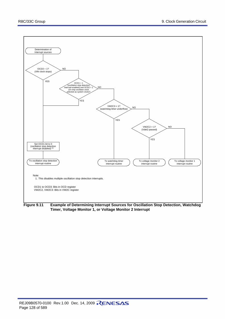
R8C/33C Group 9. Clock Generation Circuit
REJ09B0570-0100 Rev.1.00 Dec. 14, 2009Page 128 of 589
Figure 9.11 Example of Determining Interrupt Sources for Oscillation Stop Detection, Watchdog Timer, Voltage Monitor 1, or Voltage Monitor 2 Interrupt
Determination ofInterrupt sources
OCD3 = 1?(XIN clock stops)
OCD1 = 1(oscillation stop detection
interrupt enabled) and OCD2 = 1(on-chip oscillator clock
selected as system clock)?
VW2C3 = 1?(watchdog timer underflow)
VW2C2 = 1?(Vdet2 passed)
To oscillation stop detectioninterrupt routine
To voltage monitor 1interrupt routine
To voltage monitor 2interrupt routine
To watchdog timerinterrupt routine
NO
YES
NO
YES
NO
YES
NO
YES
Note:1. This disables multiple oscillation stop detection interrupts.
OCD1 to OCD3: Bits in OCD registerVW2C2, VW2C3: Bits in VW2C register
Set OCD1 bit to 0(oscillation stop detection
interrupt disabled) (1)

R8C/33C Group 9. Clock Generation Circuit
REJ09B0570-0100 Rev.1.00 Dec. 14, 2009Page 129 of 589
9.9 Notes on Clock Generation Circuit
9.9.1 Stop ModeTo enter stop mode, set the FMR01 bit in the FMR0 register to 0 (CPU rewrite mode disabled) and then theCM10 bit in the CM1 register to 1 (stop mode). An instruction queue pre-reads 4 bytes from the instructionwhich sets the CM10 bit to 1 (stop mode) and the program stops.Insert at least four NOP instructions following the JMP.B instruction after the instruction which sets the CM10bit to 1.
• Program example to enter stop modeBCLR 1,FMR0 ; CPU rewrite mode disabledBCLR 7,FMR2 ; Low-current-consumption read mode disabledBSET 0,PRCR ; Writing to CM1 register enabledFSET I ; Interrupt enabledBSET 0,CM1 ; Stop modeJMP.B LABEL_001
LABEL_001:NOPNOPNOPNOP
9.9.2 Wait ModeTo enter wait mode by setting the CM30 bit to 1, set the FMR01 bit in the FMR0 register to 0 (CPU rewritemode disabled) before setting the CM30 bit to 1.To enter wait mode with the WAIT instruction, set the FMR01 bit in the FMR0 register to 0 (CPU rewrite modedisabled) and then execute the WAIT instruction. An instruction queue pre-reads 4 bytes from the instruction toset the CM30 bit to 1 (MCU enters wait mode) or the WAIT instruction, and then the program stops. Insert atleast four NOP instructions after the instruction to set the CM30 bit to 1 (MCU enters wait mode) or the WAITinstruction.
• Program example to execute the WAIT instructionBCLR 1,FMR0 ; CPU rewrite mode disabledBCLR 7,FMR2 ; Low-current-consumption read mode disabledFSET I ; Interrupt enabledWAIT ; Wait modeNOPNOPNOPNOP
• Program example to execute the instruction to set the CM30 bit to 1BCLR 1, FMR0 ; CPU rewrite mode disabledBCLR 7,FMR2 ; Low-current-consumption read mode disabledBSET 0, PRCR ; Writing to CM3 register enabledFCLR I ; Interrupt disabledBSET 0, CM3 ; Wait modeNOPNOPNOPNOPBCLR 0, PRCR ; Writing to CM3 register disabledFSET I ; Interrupt enabled

R8C/33C Group 9. Clock Generation Circuit
REJ09B0570-0100 Rev.1.00 Dec. 14, 2009Page 130 of 589
9.9.3 Oscillation Stop Detection FunctionSince the oscillation stop detection function cannot be used if the XIN clock frequency is below 2 MHz, set bitsOCD1 to OCD0 to 00b.
9.9.4 Oscillation Circuit ConstantsConsult the oscillator manufacturer to determine the optimal oscillation circuit constants for the user system.To use the MCU with supply voltage below VCC = 2.7 V, it is recommended to set the CM11 bit in the CM1register to 1 (on-chip feedback resistor disabled) and connect the feedback resistor to the chip externally.

R8C/33C Group 10. Protection
REJ09B0570-0100 Rev.1.00 Dec. 14, 2009Page 131 of 589
10. ProtectionThe protection function protects important registers from being easily overwritten if a program runs out of control.The registers protected by the PRCR register are as follows:• Registers protected by PRC0 bit: Registers CM0, CM1, CM3, OCD, FRA0, FRA1, FRA2, and FRA3• Registers protected by PRC1 bit: Registers PM0 and PM1• Registers protected by PRC2 bit: PD0 register• Registers protected by PRC3 bit: Registers OCVREFCR, VCA2, VD1LS, VW0C, VW1C, and VW2C
10.1 Register
10.1.1 Protect Register (PRCR)
Notes:1. The PRC2 bit is set to 0 after setting it to 1 (write enabled) and writing to the SFR area. Change the register
protected by the PRC2 bit with the next instruction after that used to set the PRC2 bit to 1. Do not allow interruptsor DTC activation between the instruction to set to the PRC2 bit to 1 and the next instruction.
2. Bits PRC0, PRC1, and PRC3 are not set to 0 even after setting them to 1 (write enabled) and writing to the SFRareas. Set these bits to 0 by a program.
Address 000AhBit b7 b6 b5 b4 b3 b2 b1 b0
Symbol — — — — PRC3 PRC2 PRC1 PRC0After Reset 0 0 0 0 0 0 0 0
Bit Symbol Bit Name Function R/Wb0 PRC0 Protect bit 0 Enables writing to registers CM0, CM1, CM3, OCD, FRA0,
FRA1, FRA2, and FRA3.0: Write disabled1: Write enabled (2)
R/W
b1 PRC1 Protect bit 1 Enables writing to registers PM0 and PM1.0: Write disabled1: Write enabled (2)
R/W
b2 PRC2 Protect bit 2 Enables writing to the PD0 register.0: Write disabled1: Write enabled (1)
R/W
b3 PRC3 Protect bit 3 Enables writing to registers OCVREFCR, VCA2, VD1LS, VW0C, VW1C, and VW2C.0: Write disabled1: Write enabled (2)
R/W
b4 — Reserved bits Set to 0. R/Wb5 —b6 —b7 — Nothing is assigned. If necessary, set to 0. When read, the content is 0. —

R8C/33C Group 11. Interrupts
REJ09B0570-0100 Rev.1.00 Dec. 14, 2009Page 132 of 589
11. Interrupts
11.1 Overview
11.1.1 Types of InterruptsFigure 11.1 shows the Types of Interrupts.
Figure 11.1 Types of Interrupts
• Maskable interrupts: These interrupts are enabled or disabled by the interrupt enable flag (I flag).The interrupt priority can be changed based on the interrupt priority level.
• Non-maskable interrupts: These interrupts are not enabled or disabled by the interrupt enable flag (I flag).The interrupt priority cannot be changed based on the interrupt priority level.
Interrupts
(non-maskable interrupts)
Hardware
Software
(non-maskable interrupts)
(maskable interrupts)
Special
Peripheral function (1)
Undefined instruction (UND instruction)Overflow (INTO instruction)BRK instructionINT instruction
Watchdog timerOscillation stop detectionVoltage monitor 1 (3)
Voltage monitor 2 (3)
Single step (2)
Address break (2)
Address match
Notes: 1. Peripheral function interrupts are generated by the peripheral functions in the MCU. 2. Do not use these interrupts. This is provided exclusively for use by development tools. 3. A non-maskable or maskable interrupt can be selected by bits IRQ1SEL and IRQ2SEL in the CMPA register.

R8C/33C Group 11. Interrupts
REJ09B0570-0100 Rev.1.00 Dec. 14, 2009Page 133 of 589
11.1.2 Software InterruptsA software interrupt is generated when an instruction is executed. Software interrupts are non-maskable.
11.1.2.1 Undefined Instruction InterruptAn undefined instruction interrupt is generated when the UND instruction is executed.
11.1.2.2 Overflow InterruptAn overflow interrupt is generated when the O flag is set to 1 (arithmetic operation overflow) and the INTOinstruction is executed. Instructions that set the O flag are as follows: ABS, ADC, ADCF, ADD, CMP, DIV, DIVU, DIVX, NEG, RMPA, SBB, SHA, and SUB.
11.1.2.3 BRK InterruptA BRK interrupt is generated when the BRK instruction is executed.
11.1.2.4 INT Instruction InterruptAn INT instruction interrupt is generated when the INT instruction is executed. Software interrupt numbers 0 to63 can be specified with the INT instruction. Because some software interrupt numbers are assigned toperipheral function interrupts, the same interrupt routine as for peripheral function interrupts can be executed byexecuting the INT instruction. For software interrupt numbers 0 to 31, the U flag is saved on the stack during instruction execution and the Uflag is set to 0 (ISP selected) before the interrupt sequence is executed. The U flag is restored from the stackwhen returning from the interrupt routine. For software interrupt numbers 32 to 63, the U flag does not changestate during instruction execution, and the selected SP is used.

R8C/33C Group 11. Interrupts
REJ09B0570-0100 Rev.1.00 Dec. 14, 2009Page 134 of 589
11.1.3 Special InterruptsSpecial interrupts are non-maskable.
11.1.3.1 Watchdog Timer InterruptA watchdog timer interrupt is generated by the watchdog timer. For details, refer to 14. Watchdog Timer.
11.1.3.2 Oscillation Stop Detection InterruptAn oscillation stop detection interrupt is generated by the oscillation stop detection function. For details of theoscillation stop detection function, refer to 9. Clock Generation Circuit.
11.1.3.3 Voltage Monitor 1 InterruptA voltage monitor 1 interrupt is generated by the voltage detection circuit. A non-maskable or maskableinterrupt can be selected by IRQ1SEL bit in the CMPA register. For details of the voltage detection circuit,refer to 6. Voltage Detection Circuit.
11.1.3.4 Voltage Monitor 2 InterruptA voltage monitor 2 interrupt is generated by the voltage detection circuit. A non-maskable or maskableinterrupt can be selected by IRQ2SEL bit in the CMPA register. For details of the voltage detection circuit,refer to 6. Voltage Detection Circuit.
11.1.3.5 Single-Step Interrupt, and Address Break InterruptDo not use these interrupts. They are provided exclusively for use by development tools.
11.1.3.6 Address Match InterruptAn address match interrupt is generated immediately before executing an instruction that is stored at an addressindicated by registers RMAD0 to RMAD1 if the AIER00 bit in the AIER0 register or the AIER10 bit in theAIER1 register is set to 1 (address match interrupt enabled). For details of the address match interrupt, refer to 11.6 Address Match Interrupt.
11.1.4 Peripheral Function InterruptsA peripheral function interrupt is generated by a peripheral function in the MCU. Peripheral function interruptsare maskable. Refer to Table 11.2 Relocatable Vector Tables for sources of the corresponding peripheralfunction interrupt. For details of peripheral functions, refer to the descriptions of individual peripheralfunctions.

R8C/33C Group 11. Interrupts
REJ09B0570-0100 Rev.1.00 Dec. 14, 2009Page 135 of 589
11.1.5 Interrupts and Interrupt VectorsThere are 4 bytes in each vector. Set the starting address of an interrupt routine in each interrupt vector. Whenan interrupt request is acknowledged, the CPU branches to the address set in the corresponding interrupt vector.Figure 11.2 shows an Interrupt Vector.
Figure 11.2 Interrupt Vector
11.1.5.1 Fixed Vector TablesThe fixed vector tables are allocated addresses 0FFDCh to 0FFFFh.Table 11.1 lists the Fixed Vector Tables. The vector addresses (H) of fixed vectors are used by the ID codecheck function. For details, refer to 30.3 Functions to Prevent Flash Memory from being Rewritten.
Note:1. Do not use these interrupts. They are provided exclusively for use by development tools.
Table 11.1 Fixed Vector Tables
Interrupt Source Vector Addresses Address (L) to (H) Remarks Reference
Undefined instruction 0FFDCh to 0FFDFh Interrupt with UND instruction
R8C/Tiny Series Software Manual
Overflow 0FFE0h to 0FFE3h Interrupt with INTO instruction
BRK instruction 0FFE4h to 0FFE7h If the content of address 0FFE7h is FFh, program execution starts from the address shown by the vector in the relocatable vector table.
Address match 0FFE8h to 0FFEBh 11.6 Address Match Interrupt
Single step (1) 0FFECh to 0FFEFhWatchdog timer, Oscillation stop detection, Voltage monitor 1, Voltage monitor 2
0FFF0h to 0FFF3h 14. Watchdog Timer9. Clock Generation Circuit6. Voltage Detection Circuit
Address break (1) 0FFF4h to 0FFF7h(Reserved) 0FFF8h to 0FFFBhReset 0FFFCh to 0FFFFh 5. Resets
Vector address (L)
Vector address (H)
MSB LSB
Low-order address
Middle-order address
High-order address0 0 0 0
0 0 0 0 0 0 0 0

R8C/33C Group 11. Interrupts
REJ09B0570-0100 Rev.1.00 Dec. 14, 2009Page 136 of 589
11.1.5.2 Relocatable Vector TablesThe relocatable vector tables occupy 256 bytes beginning from the starting address set in the INTB register.Table 11.2 lists the Relocatable Vector Tables.
Notes:1. These addresses are relative to those in the INTB register.2. Selectable by the IICSEL bit in the SSUIICSR register.3. These interrupts are not disabled by the I flag.
11.2 Registers
Table 11.2 Relocatable Vector Tables
Interrupt Source Vector Addresses (1)
Address (L) to Address (H)
Software Interrupt Number
Interrupt Control Register Reference
BRK instruction (3) +0 to +3 (0000h to 0003h) 0 − R8C/Tiny Series Software Manual
Flash memory ready +4 to +7 (0004h to 0007h) 1 FMRDYIC 30. Flash Memory(Reserved) 2 to 5 − −(Reserved) +24 to +27 (0018h to 001Bh) 6 − −Timer RC +28 to +31 (001Ch to 001Fh) 7 TRCIC 19. Timer RC(Reserved) +32 to +35 (0020h to 0023h) 8 − −(Reserved) +36 to +39 (0024h to 0027h) 9 − −Timer RE +40 to +43 (0028h to 002Bh) 10 TREIC 20. Timer REUART2 transmit/NACK2 +44 to +47 (002Ch to 002Fh) 11 S2TIC 22. Serial Interface
(UART2)UART2 receive/ACK2 +48 to +51 (0030h to 0033h) 12 S2RICKey input +52 to +55 (0034h to 0037h) 13 KUPIC 11.5 Key Input InterruptA/D conversion +56 to +59 (0038h to 003Bh) 14 ADIC 27. A/D ConverterSynchronous serial communication unit / I2C bus interface (2)
+60 to +63 (003Ch to 003Fh) 15 SSUIC/IICIC 24. Synchronous Serial Communication Unit (SSU),
25. I2C bus Interface(Reserved) 16 − −UART0 transmit +68 to +71 (0044h to 0047h) 17 S0TIC 21. Serial Interface
(UARTi (i = 0 or 1))UART0 receive +72 to +75 (0048h to 004Bh) 18 S0RICUART1 transmit +76 to +79 (004Ch to 004Fh) 19 S1TICUART1 receive +80 to +83 (0050h to 0053h) 20 S1RIC(Reserved) +84 to +87 (0054h to 0057h) 21 − −Timer RA +88 to +91 (0058h to 005Bh) 22 TRAIC 17. Timer RA(Reserved) 23 − −Timer RB +96 to +99 (0060h to 0063h) 24 TRBIC 18. Timer RBINT1 +100 to +103 (0064h to 0067h) 25 INT1IC 11.4 INT InterruptINT3 +104 to +107 (0068h to 006Bh) 26 INT3IC(Reserved) 27 − −(Reserved) 28 − −
INT0 +116 to +119 (0074h to 0077h) 29 INT0IC 11.4 INT InterruptUART2 bus collision detection +120 to +123 (0078h to 007Bh) 30 U2BCNIC 22. Serial Interface
(UART2)(Reserved) 31 − −Software (3) +128 to +131 (0080h to 0083h) to
+164 to +167 (00A4h to 00A7h)32 to 41 − R8C/Tiny Series
Software Manual(Reserved) 42 to 49 − −Voltage monitor 1 +200 to +203 (00C8h to 00CBh) 50 VCMP1IC 6. Voltage Detection
CircuitVoltage monitor 2 +204 to +207 (00CCh to 00CFh) 51 VCMP2IC(Reserved) 52 to 55 − −Software (3) +224 to +227 (00E0h to 00E3h) to
+252 to +255 (00FCh to 00FFh)56 to 63 − R8C/Tiny Series
Software Manual

R8C/33C Group 11. Interrupts
REJ09B0570-0100 Rev.1.00 Dec. 14, 2009Page 137 of 589
11.2.1 Interrupt Control Register(TREIC, S2TIC, S2RIC, KUPIC, ADIC, S0TIC, S0RIC, S1TIC, S1RIC, TRAIC,TRBIC, U2BCNIC, VCMP1IC, VCMP2IC)
Note:1. Only 0 can be written to the IR bit. Do not write 1 to this bit.
Rewrite the interrupt control register when an interrupt request corresponding to the register is not generated.Refer to 11.8.5 Rewriting Interrupt Control Register.
Address 004Ah (TREIC), 004Bh (S2TIC), 004Ch (S2RIC), 004Dh (KUPIC), 004Eh (ADIC), 0051h (S0TIC), 0052h (S0RIC), 0053h (S1TIC), 0054h (S1RIC), 0056h (TRAIC), 0058h (TRBIC), 005Eh (U2BCNIC), 0072h (VCMP1IC), 0073h (VCMP2IC),
Bit b7 b6 b5 b4 b3 b2 b1 b0Symbol — — — — IR ILVL2 ILVL1 ILVL0
After Reset X X X X X 0 0 0
Bit Symbol Bit Name Function R/Wb0 ILVL0 Interrupt priority level select bit b2 b1 b0
0 0 0: Level 0 (interrupt disabled) 0 0 1: Level 1 0 1 0: Level 2 0 1 1: Level 3 1 0 0: Level 4 1 0 1: Level 5 1 1 0: Level 6 1 1 1: Level 7
R/Wb1 ILVL1 R/Wb2 ILVL2 R/W
b3 IR Interrupt request bit 0: No interrupt requested1: Interrupt requested
R/W(1)
b4 — Nothing is assigned. If necessary, set to 0.When read, the content is undefined.
—b5 —b6 —b7 —

R8C/33C Group 11. Interrupts
REJ09B0570-0100 Rev.1.00 Dec. 14, 2009Page 138 of 589
11.2.2 Interrupt Control Register (FMRDYIC, TRCIC, SSUIC/IICIC)
Note:1. Selectable by the IICSEL bit in the SSUIICSR register.
Rewrite the interrupt control register when an interrupt request corresponding to the register is not generated.Refer to 11.8.5 Rewriting Interrupt Control Register.
Address 0041h (FMRDYIC), 0047h (TRCIC), 004Fh (SSUIC/IICIC (1))Bit b7 b6 b5 b4 b3 b2 b1 b0
Symbol — — — — IR ILVL2 ILVL1 ILVL0After Reset X X X X X 0 0 0
Bit Symbol Bit Name Function R/Wb0 ILVL0 Interrupt priority level select bit b2 b1 b0
0 0 0: Level 0 (interrupt disabled) 0 0 1: Level 1 0 1 0: Level 2 0 1 1: Level 3 1 0 0: Level 4 1 0 1: Level 5 1 1 0: Level 6 1 1 1: Level 7
R/Wb1 ILVL1 R/Wb2 ILVL2 R/W
b3 IR Interrupt request bit 0: No interrupt requested1: Interrupt requested
R
b4 — Nothing is assigned. If necessary, set to 0.When read, the content is undefined.
—b5 —b6 —b7 —

R8C/33C Group 11. Interrupts
REJ09B0570-0100 Rev.1.00 Dec. 14, 2009Page 139 of 589
11.2.3 INTi Interrupt Control Register (INTiIC) (i = 0, 1, 3)
Notes:1. Only 0 can be written to the IR bit. (Do not write 1 to this bit.)2. If the INTiPL bit in the INTEN register is set to 1 (both edges), set the POL bit to 0 (falling edge selected).3. The IR bit may be set to 1 (interrupt requested) when the POL bit is rewritten. Refer to 11.8.4 Changing
Interrupt Sources.
Rewrite the interrupt control register when an interrupt request corresponding to the register is not generated.Refer to 11.8.5 Rewriting Interrupt Control Register.
Address 0059h (INT1IC), 005Ah (INT3IC), 005Dh (INT0IC)Bit b7 b6 b5 b4 b3 b2 b1 b0
Symbol — — — POL IR ILVL2 ILVL1 ILVL0After Reset X X 0 0 X 0 0 0
Bit Symbol Bit Name Function R/Wb0 ILVL0 Interrupt priority level select bit b2 b1 b0
0 0 0: Level 0 (interrupt disabled) 0 0 1: Level 1 0 1 0: Level 2 0 1 1: Level 3 1 0 0: Level 4 1 0 1: Level 5 1 1 0: Level 6 1 1 1: Level 7
R/Wb1 ILVL1 R/Wb2 ILVL2 R/W
b3 IR Interrupt request bit 0: No interrupt requested1: Interrupt requested
R/W(1)
b4 POL Polarity switch bit (3) 0: Falling edge selected1: Rising edge selected (2)
R/W
b5 — Reserved bit Set to 0. R/Wb6 — Nothing is assigned. If necessary, set to 0.
When read, the content is undefined.—
b7 —

R8C/33C Group 11. Interrupts
REJ09B0570-0100 Rev.1.00 Dec. 14, 2009Page 140 of 589
11.3 Interrupt ControlThe following describes enabling and disabling maskable interrupts and setting the acknowledgement priority.This description does not apply to non-maskable interrupts.Use the I flag in the FLG register, IPL, and bits ILVL2 to ILVL0 in the corresponding interrupt control registerto enable or disable a maskable interrupt. Whether an interrupt is requested or not is indicated by the IR bit inthe corresponding interrupt control register.
11.3.1 I FlagThe I flag enables or disables maskable interrupts. Setting the I flag to 1 (enabled) enables maskable interrupts.Setting the I flag to 0 (disabled) disables all maskable interrupts.
11.3.2 IR BitThe IR bit is set to 1 (interrupt requested) when an interrupt request is generated. After the interrupt request isacknowledged and the CPU branches to the corresponding interrupt vector, the IR bit is set to 0 (no interruptrequested).The IR bit can be set to 0 by a program. Do not write 1 to this bit.However, the IR bit operations of the timer RC interrupt, the synchronous serial communication unit interrupt,the I2C bus interface interrupt, and the flash memory interrupt are different. Refer to 11.7 Timer RC Interrupt,Synchronous Serial Communication Unit Interrupt, I2C bus Interface Interrupt, and Flash MemoryInterrupt (Interrupts with Multiple Interrupt Request Sources).
11.3.3 Bits ILVL2 to ILVL0, IPLInterrupt priority levels can be set using bits ILVL2 to ILVL0.Table 11.3 lists the Settings of Interrupt Priority Levels and Table 11.4 lists the Interrupt Priority LevelsEnabled by IPL.
The following are the conditions when an interrupt is acknowledged:• I flag = 1• IR bit = 1• Interrupt priority level > IPL
The I flag, IR bit, bits ILVL2 to ILVL0, and IPL are independent of each other. They do not affect one another.
Table 11.3 Settings of Interrupt Priority Levels
Bits ILVL2 to ILVL0 Interrupt Priority Level Priority000b Level 0 (interrupt disabled) −001b Level 1 Low010b Level 2011b Level 3100b Level 4101b Level 5110b Level 6111b Level 7 High
Table 11.4 Interrupt Priority Levels Enabled by IPL
IPL Enabled Interrupt Priority Level000b Interrupt level 1 and above001b Interrupt level 2 and above010b Interrupt level 3 and above011b Interrupt level 4 and above100b Interrupt level 5 and above101b Interrupt level 6 and above110b Interrupt level 7 and above111b All maskable interrupts are disabled

R8C/33C Group 11. Interrupts
REJ09B0570-0100 Rev.1.00 Dec. 14, 2009Page 141 of 589
11.3.4 Interrupt SequenceThe following describes an interrupt sequence which is performed from when an interrupt request isacknowledged until the interrupt routine is executed. When an interrupt request is generated while an instruction is being executed, the CPU determines its interruptpriority level after the instruction is completed. The CPU starts the interrupt sequence from the following cycle.However, for the SMOVB, SMOVF, SSTR, or RMPA instruction, if an interrupt request is generated while theinstruction is being executed, the MCU suspends the instruction to start the interrupt sequence. The interruptsequence is performed as indicated below.Figure 11.3 shows the Time Required for Executing Interrupt Sequence.
(1) The CPU obtains interrupt information (interrupt number and interrupt request level) by reading address00000h. The IR bit for the corresponding interrupt is set to 0 (no interrupt requested). (2)
(2) The FLG register is saved to a temporary register (1) in the CPU immediately before entering the interruptsequence.
(3) The I, D and U flags in the FLG register are set as follows:The I flag is set to 0 (interrupts disabled).The D flag is set to 0 (single-step interrupt disabled).The U flag is set to 0 (ISP selected).However, the U flag does not change state if an INT instruction for software interrupt number 32 to 63 isexecuted.
(4) The CPU internal temporary register (1) is saved on the stack.(5) The PC is saved on the stack.(6) The interrupt priority level of the acknowledged interrupt is set in the IPL.(7) The starting address of the interrupt routine set in the interrupt vector is stored in the PC.
After the interrupt sequence is completed, instructions are executed from the starting address of the interruptroutine.
Figure 11.3 Time Required for Executing Interrupt Sequence
Notes:1. These registers cannot be accessed by the user.2. Refer to 11.7 Timer RC Interrupt, Synchronous Serial Communication Unit Interrupt, I2C bus
Interface Interrupt, and Flash Memory Interrupt (Interrupts with Multiple Interrupt Request Sources) for the IR bit operations of the timer RC Interrupt, the Synchronous Serial Communication unit Interrupt, and the I2C bus Interface Interrupt.
1 2 3 4 5 6 7 8 9 10 11 12 13 14 15 16 17 18 19 20CPU Clock
Address Bus
Data Bus
RD
WR
Address0000h Undefined
Undefined
Undefined
Interruptinformation
SP-2 SP-1 SP-4 SP-3 VEC VEC+1 VEC+2 PC
SP-2contents
SP-1contents
SP-4contents
SP-3 contents
VECcontents
VEC+1contents
VEC+2contents
Note: The indeterminate state depends on the instruction queue buffer. A read cycle occurs when the instruction queue buffer is ready to acknowledge instructions.
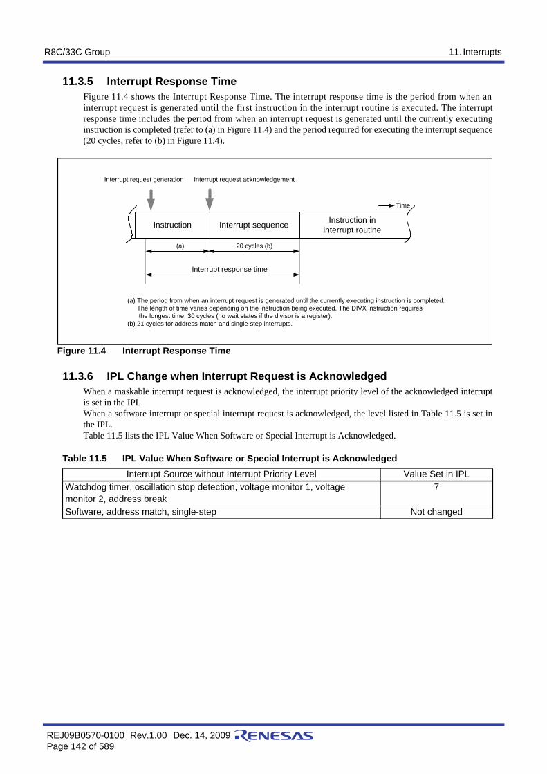
R8C/33C Group 11. Interrupts
REJ09B0570-0100 Rev.1.00 Dec. 14, 2009Page 142 of 589
11.3.5 Interrupt Response TimeFigure 11.4 shows the Interrupt Response Time. The interrupt response time is the period from when aninterrupt request is generated until the first instruction in the interrupt routine is executed. The interruptresponse time includes the period from when an interrupt request is generated until the currently executinginstruction is completed (refer to (a) in Figure 11.4) and the period required for executing the interrupt sequence(20 cycles, refer to (b) in Figure 11.4).
Figure 11.4 Interrupt Response Time
11.3.6 IPL Change when Interrupt Request is AcknowledgedWhen a maskable interrupt request is acknowledged, the interrupt priority level of the acknowledged interruptis set in the IPL.When a software interrupt or special interrupt request is acknowledged, the level listed in Table 11.5 is set inthe IPL.Table 11.5 lists the IPL Value When Software or Special Interrupt is Acknowledged.
Table 11.5 IPL Value When Software or Special Interrupt is AcknowledgedInterrupt Source without Interrupt Priority Level Value Set in IPL
Watchdog timer, oscillation stop detection, voltage monitor 1, voltage monitor 2, address break
7
Software, address match, single-step Not changed
Interrupt request generation Interrupt request acknowledgement
Instruction Interrupt sequence Instruction ininterrupt routine
Time
(a) 20 cycles (b)
Interrupt response time
(a) The period from when an interrupt request is generated until the currently executing instruction is completed.The length of time varies depending on the instruction being executed. The DIVX instruction requires the longest time, 30 cycles (no wait states if the divisor is a register).
(b) 21 cycles for address match and single-step interrupts.

R8C/33C Group 11. Interrupts
REJ09B0570-0100 Rev.1.00 Dec. 14, 2009Page 143 of 589
11.3.7 Saving RegistersIn the interrupt sequence, the FLG register and PC are saved on the stack.After an extended 16 bits, 4 high-order bits in the PC and 4 high-order (IPL) and 8 low-order bits in the FLGregister, are saved on the stack, the 16 low-order bits in the PC are saved.Figure 11.5 shows the Stack State Before and After Acknowledgement of Interrupt Request.The other necessary registers should be saved by a program at the beginning of the interrupt routine. ThePUSHM instruction can save several registers in the register bank being currently used (1) with a singleinstruction.
Note:1. Selectable from registers R0, R1, R2, R3, A0, A1, SB, and FB.
Figure 11.5 Stack State Before and After Acknowledgement of Interrupt Request
Stack
[SP]SP value beforeinterrupt requestacknowledgement (1)
Previous stack contents
LSBMSBAddress
Previous stack contents
m−4
m−3
m−2
m−1
m
m+1
Stack state before interrupt request acknowledgement
[SP]New SP value (1)
Previous stack contents
LSBMSB
Previous stack contents
m
m+1
Stack state after interrupt request acknowledgement
PCL
PCM
FLGL
FLGH PCH
m−4
m−3
m−2
m−1
StackAddress
PCL : 8 low-order bits of PCPCM : 8 middle-order bits of PCPCH : 4 high-order bits of PCFLGL : 8 low-order bits of FLGFLGH : 4 high-order bits of FLG
Note: 1.When an INT instruction for software numbers 32 to 63 has been executed, this SP is indicated by the U flag. Otherwise it is ISP.

R8C/33C Group 11. Interrupts
REJ09B0570-0100 Rev.1.00 Dec. 14, 2009Page 144 of 589
The register saving operation, which is performed as part of the interrupt sequence, saved in 8 bits at a time infour steps.Figure 11.6 shows the Register Saving Operation.
Figure 11.6 Register Saving Operation
Stack
Completed saving registersin four operations
Address
[SP]−5
[SP]
PCL
PCM
FLGL
FLGH PCH
(3)
(4)
(1)
(2)
Saved, 8 bits at a time
Sequence in which registers are saved
Note:1.[SP] indicates the SP initial value when an interrupt request is acknowledged.
After registers are saved, the SP content is [SP] minus 4. When an INT instruction for software numbers 32 to 63 has been executed, this SP is indicated by the U flag. Otherwise it is ISP.
[SP]−4
[SP]−3
[SP]−2
[SP]−1PCL : 8 low-order bits of PCPCM : 8 middle-order bits of PCPCH : 4 high-order bits of PCFLGL : 8 low-order bits of FLGFLGH : 4 high-order bits of FLG

R8C/33C Group 11. Interrupts
REJ09B0570-0100 Rev.1.00 Dec. 14, 2009Page 145 of 589
11.3.8 Returning from Interrupt RoutineWhen the REIT instruction is executed at the end of an interrupt routine, the FLG register and PC, which havebeen saved on the stack, are automatically restored. The program, that was running before the interrupt requestwas acknowledged, starts running again.Registers saved by a program in an interrupt routine should be saved using the POPM instruction or a similarinstruction before executing the REIT instruction.
11.3.9 Interrupt PriorityIf two or more interrupt requests are generated while a single instruction is being executed, the interrupt withthe higher priority is acknowledged. Set bits ILVL2 to ILVL0 to select any priority level for maskable interrupts (peripheral function). However, iftwo or more maskable interrupts have the same priority level, their interrupt priority is resolved by hardware,with the higher priority interrupts acknowledged.The priority of watchdog timer and other special interrupts is set by hardware.Figure 11.7 shows the Hardware Interrupt Priority.Software interrupts are not affected by the interrupt priority. If an instruction is executed, the MCU executes theinterrupt routine.
Figure 11.7 Hardware Interrupt Priority
Address break
Watchdog timerOscillation stop detection
Voltage monitor 1Voltage monitor 2
Peripheral function
Single step
Address match
High
Low
Reset

R8C/33C Group 11. Interrupts
REJ09B0570-0100 Rev.1.00 Dec. 14, 2009Page 146 of 589
11.3.10 Interrupt Priority Level Selection CircuitThe interrupt priority level selection circuit is used to select the highest priority interrupt.Figure 11.8 shows the Interrupt Priority Level Selection Circuit.
Figure 11.8 Interrupt Priority Level Selection Circuit
Timer RA
INT0
Timer RC
UART1 transmit
UART0 transmit
SSU / I2C bus (1)
Flash memory ready
Lowest
Highest
Peripheral function interrupt priority(if the priority levels are same)
Interrupt request levelselection output signal
Interrupt requestacknowledgementI flag
Address match
Watchdog timer
Oscillation stop detection
Voltage monitor 1
Note: 1. Selectable by the IICSEL bit in the SSUIICSR register.
UART2 receive/ACK2
Timer RE
UART0 receive
A/D conversion
UART2 transmit/NACK2
UART1 receive
INT3
Voltage monitor 1
Priority level of interruptsLevel 0 (initial value)
Voltage monitor 2
Voltage monitor 2
Timer RB
INT1
Key input
UART2 bus collision detection
IPL

R8C/33C Group 11. Interrupts
REJ09B0570-0100 Rev.1.00 Dec. 14, 2009Page 147 of 589
11.4 INT Interrupt
11.4.1 INTi Interrupt (i = 0, 1, 3)The INTi interrupt is generated by an INTi input. To use the INTi interrupt, set the INTiEN bit in the INTENregister is to 1 (enabled). The edge polarity is selected using the INTiPL bit in the INTEN register and the POLbit in the INTiIC register. The input pins used as the INT1 input can be selected. Also, inputs can be passed through a digital filter with three different sampling clocks. The INT0 pin is shared with the pulse output forced cutoff input of timer RC, and the external trigger input oftimer RB.Table 11.6 lists the Pin Configuration of INT Interrupt.
11.4.2 INT Interrupt Input Pin Select Register (INTSR)
The INTSR register selects which pin is assigned to the INT1 input. To use INT1, set this register. Set the INTSR register before setting the INT1 associated registers. Also, do not change the setting values inthis register during INT1 operation.
Table 11.6 Pin Configuration of INT Interrupt
Pin Name Assigned Pin I/O Function
INT0 P4_5 Input INT0 interrupt input, timer RB external trigger input, timer RC pulse output forced cutoff input
INT1 P1_5, P1_7, or P2_0 Input INT1 interrupt input
INT3 P3_3 Input INT3 interrupt input
Address 018EhBit b7 b6 b5 b4 b3 b2 b1 b0
Symbol — — — — INT1SEL2 INT1SEL1 INT1SEL0 —After Reset 0 0 0 0 0 0 0 0
Bit Symbol Bit Name Function R/Wb0 — Nothing is assigned. If necessary, set to 0. When read, the content is 0. —b1 INT1SEL0 INT1 pin select bit b3 b2 b1
0 0 0: P1_7 assigned 0 0 1: P1_5 assigned 0 1 0: P2_0 assignedOther than above: Do not set.
R/Wb2 INT1SEL1 R/Wb3 INT1SEL2 R/W
b4 — Reserved bit Set to 0. R/Wb5 — Nothing is assigned. If necessary, set to 0. When read, the content is 0. —b6 — Reserved bits Set to 0. R/Wb7 —

R8C/33C Group 11. Interrupts
REJ09B0570-0100 Rev.1.00 Dec. 14, 2009Page 148 of 589
11.4.3 External Input Enable Register 0 (INTEN)
Notes:1. To set the INTiPL bit (i = 0, 1, 3) to 1 (both edges), set the POL bit in the INTiIC register to 0 (falling edge
selected).2. The IR bit in the INTiIC register may be set to 1 (interrupt requested) if the INTEN register is rewritten. Refer to
11.8.4 Changing Interrupt Sources.
11.4.4 INT Input Filter Select Register 0 (INTF)
Address 01FAhBit b7 b6 b5 b4 b3 b2 b1 b0
Symbol INT3PL INT3EN — — INT1PL INT1EN INT0PL INT0ENAfter Reset 0 0 0 0 0 0 0 0
Bit Symbol Bit Name Function R/Wb0 INT0EN INT0 input enable bit 0: Disabled
1: EnabledR/W
b1 INT0PL INT0 input polarity select bit (1, 2) 0: One edge1: Both edges
R/W
b2 INT1EN INT1 input enable bit 0: Disabled1: Enabled
R/W
b3 INT1PL INT1 input polarity select bit (1, 2) 0: One edge1: Both edges
R/W
b4 — Reserved bits Set to 0. R/Wb5 —b6 INT3EN INT3 input enable bit 0: Disabled
1: EnabledR/W
b7 INT3PL INT3 input polarity select bit (1, 2) 0: One edge1: Both edges
R/W
Address 01FChBit b7 b6 b5 b4 b3 b2 b1 b0
Symbol INT3F1 INT3F0 — — INT1F1 INT1F0 INT0F1 INT0F0After Reset 0 0 0 0 0 0 0 0
Bit Symbol Bit Name Function R/Wb0 INT0F0 INT0 input filter select bit b1 b0
0 0: No filter 0 1: Filter with f1 sampling 1 0: Filter with f8 sampling 1 1: Filter with f32 sampling
R/Wb1 INT0F1 R/W
b2 INT1F0 INT1 input filter select bit b3 b2 0 0: No filter 0 1: Filter with f1 sampling 1 0: Filter with f8 sampling 1 1: Filter with f32 sampling
R/Wb3 INT1F1 R/W
b4 — Reserved bits Set to 0. R/Wb5 —b6 INT3F0 INT3 input filter select bit b7 b6
0 0: No filter 0 1: Filter with f1 sampling 1 0: Filter with f8 sampling 1 1: Filter with f32 sampling
R/Wb7 INT3F1 R/W

R8C/33C Group 11. Interrupts
REJ09B0570-0100 Rev.1.00 Dec. 14, 2009Page 149 of 589
11.4.5 INTi Input Filter (i = 0, 1, 3)The INTi input contains a digital filter. The sampling clock is selected using bits INTiF1 and INTiF0 in theINTF register. The INTi level is sampled every sampling clock cycle and if the sampled input level matchesthree times, the IR bit in the INTiIC register is set to 1 (interrupt requested).Figure 11.9 shows the INTi Input Filter Configuration. Figure 11.10 shows an Operating Example of INTi InputFilter.
Figure 11.9 INTi Input Filter Configuration
Figure 11.10 Operating Example of INTi Input Filter
INTiF0, INTiF1: Bits in INTF registerINTiEN, INTiPL: Bits in INTEN registeri = 0, 1, 3
= 01b
INTi
Port directionregister (1)
Sampling clock
Digital filter(input levelmatches3 times)
INTi interrupt
= 10b= 11bf32
f8f1
INTiF1 to INTiF0
INTiEN
Other thanINTiF1 to INTiF0= 00b
= 00b INTiPL = 0
INTiPL = 1
Note: 1. INT0: Port P4_5 direction register
INT1: Port P1_5 direction register when P1_5 pin usedPort P1_7 direction register when P1_7 pin usedPort P2_0 direction register when P2_0 pin used
INT3: Port P3_3 direction register when P3_3 pin used
Both edgesdetection
circuit
INTi input
Samplingtiming
IR bit inINTiIC register
Set to 0 by a program.
Note:1. This is an operating example when bits INTiF1 to INTiF0 in the INTF register are set to 01b, 10b, or 11b
(digital filter enabled).i = 0, 1, 3

R8C/33C Group 11. Interrupts
REJ09B0570-0100 Rev.1.00 Dec. 14, 2009Page 150 of 589
11.5 Key Input InterruptA key input interrupt request is generated by one of the input edges of pins K10 to K13. The key input interrupt canbe used as a key-on wake-up function to exit wait or stop mode. The KIiEN (i = 0 to 3) bit in the KIEN register is be used to select whether or not the pins are used as the KIi input.The KIiPL bit in the KIEN register is also be used to select the input polarity. When inputting “L” to the KIi pin, which sets the KIiPL bit to 0 (falling edge), the input to the other pins K10 toK13 is not detected as interrupts. When inputting “H” to the KIi pin, which sets the KIiPL bit to 1 (rising edge), theinput to the other pins K10 to K13 is not also detected as interrupts. Figure 11.11 shows a Block Diagram of Key Input Interrupt. Table 11.7 lists the Pin Configuration of Key InputInterrupt.
Figure 11.11 Block Diagram of Key Input Interrupt
Table 11.7 Pin Configuration of Key Input InterruptPin Name I/O Function
KI0 Input KI0 interrupt input
KI1 Input KI1 interrupt input
KI2 Input KI2 interrupt input
KI3 Input KI3 interrupt input
KI3
Pull-uptransistor
KI2
Pull-uptransistor
KI3PL = 0
KI3PL = 1
PD1_3 bitKI3EN bit
PU02 bit in PUR0 register
PD1_3 bit in PD1 registerKUPIC register
Interrupt control circuit Key inputinterrupt request
KI2PL = 0
KI2PL = 1
PD1_2 bitKI2EN bit
KI1
Pull-uptransistor KI1PL = 0
KI1PL = 1
PD1_1 bitKI1EN bit
KI0
Pull-uptransistor KI0PL = 0
KI0PL = 1
PD1_0 bitKI0EN bit KI0EN, KI1EN, KI2EN, KI3EN,
KI0PL, KI1PL, KI2PL, KI3PL: Bits in KIEN registerPD1_0, PD1_1, PD1_2, PD1_3: Bits in PD1 register

R8C/33C Group 11. Interrupts
REJ09B0570-0100 Rev.1.00 Dec. 14, 2009Page 151 of 589
11.5.1 Key Input Enable Register 0 (KIEN)
The IR bit in the KUPIC register may be set to 1 (interrupt requested) when the KIEN register is rewritten. Refer to 11.8.4 Changing Interrupt Sources.
Address 01FEhBit b7 b6 b5 b4 b3 b2 b1 b0
Symbol KI3PL KI3EN KI2PL KI2EN KI1PL KI1EN KI0PL KI0ENAfter Reset 0 0 0 0 0 0 0 0
Bit Symbol Bit Name Function R/Wb0 KI0EN KI0 input enable bit 0: Disabled
1: EnabledR/W
b1 KI0PL KI0 input polarity select bit 0: Falling edge1: Rising edge
R/W
b2 KI1EN KI1 input enable bit 0: Disabled1: Enabled
R/W
b3 KI1PL KI1 input polarity select bit 0: Falling edge1: Rising edge
R/W
b4 KI2EN KI2 input enable bit 0: Disabled1: Enabled
R/W
b5 KI2PL KI2 input polarity select bit 0: Falling edge1: Rising edge
R/W
b6 KI3EN KI3 input enable bit 0: Disabled1: Enabled
R/W
b7 KI3PL KI3 input polarity select bit 0: Falling edge1: Rising edge
R/W

R8C/33C Group 11. Interrupts
REJ09B0570-0100 Rev.1.00 Dec. 14, 2009Page 152 of 589
11.6 Address Match InterruptAn address match interrupt request is generated immediately before execution of the instruction at the addressindicated by the RMADi register (i = 0 or 1). This interrupt is used as a break function by the debugger. When theon-chip debugger is used, do not set an address match interrupt (registers AIER0, AIER1, RMAD0, and RMAD1,and fixed vector tables) in the user system.
Set the starting address of any instruction in the RMADi register (i = 0 or 1). The AIERi0 bit in the AIERi registercan be used to select enable or disable the interrupt. The address match interrupt is not affected by the I flag andIPL.The PC value (refer to 11.3.7 Saving Registers) which is saved on the stack when an address match interruptrequest is acknowledged varies depending on the instruction at the address indicated by the RMADi register. (Theappropriate return address is not saved on the stack.) When returning from the address match interrupt, follow oneof the following means:• Rewrite the contents of the stack and use the REIT instruction to return.• Use an instruction such as POP to restore the stack to its previous state before the interrupt request was
acknowledged. Then use a jump instruction to return.Table 11.8 lists the PC Value Saved on Stack When Address Match Interrupt Request is Acknowledged and Table11.9 lists the Correspondence Between Address Match Interrupt Sources and Associated Registers.
Notes:1. Refer to 11.3.7 Saving Registers.2. Operation code: Refer to the R8C/Tiny Series Software Manual (REJ09B0001).
Chapter 4. Instruction Code/Number of Cycles contains diagrams showing operation code below each syntax. Operation code is shown in the bold frame in the diagrams.
Table 11.8 PC Value Saved on Stack When Address Match Interrupt Request is AcknowledgedAddress Indicated by RMADi Register (i = 0 or 1) PC Value Saved (1)
• Instruction with 2-byte operation code (2)
• Instruction with 1-byte operation code (2)
ADD.B:S #IMM8,dest SUB.B:S #IMM8,dest AND.B:S #IMM8,destOR.B:S #IMM8,dest MOV.B:S #IMM8,dest STZ #IMM8,destSTNZ #IMM8,dest STZX #IMM81,#IMM82,destCMP.B:S #IMM8,dest PUSHM src POPM destJMPS #IMM8 JSRS #IMM8MOV.B:S #IMM,dest (however, dest = A0 or A1)
Address indicated by RMADi register + 2
Instructions other than above Address indicated by RMADi register + 1
Table 11.9 Correspondence Between Address Match Interrupt Sources and Associated RegistersAddress Match Interrupt Source Address Match Interrupt Enable Bit Address Match Interrupt RegisterAddress match interrupt 0 AIER00 RMAD0Address match interrupt 1 AIER10 RMAD1

R8C/33C Group 11. Interrupts
REJ09B0570-0100 Rev.1.00 Dec. 14, 2009Page 153 of 589
11.6.1 Address Match Interrupt Enable Register i (AIERi) (i = 0 or 1)
11.6.2 Address Match Interrupt Register i (RMADi) (i = 0 or 1)
Address 01C3h (AIER0), 01C7h (AIER1)Bit b7 b6 b5 b4 b3 b2 b1 b0
Symbol — — — — — — — AIER00 AIER0 registerAfter Reset 0 0 0 0 0 0 0 0
Symbol — — — — — — — AIER10 AIER1 registerAfter Reset 0 0 0 0 0 0 0 0
Bit Symbol Bit Name Function R/Wb0 AIERi0 Address match interrupt i enable bit 0: Disabled
1: EnabledR/W
b1 — Nothing is assigned. If necessary, set to 0. When read, the content is 0. —b2 —b3 —b4 —b5 —b6 —b7 —
Address 01C2h to 01C0h (RMAD0), 01C6h to 01C4h (RMAD1)Bit b7 b6 b5 b4 b3 b2 b1 b0
Symbol — — — — — — — —After Reset X X X X X X X X
Bit b15 b14 b13 b12 b11 b10 b9 b8Symbol — — — — — — — —
After Reset X X X X X X X X
Bit b23 b22 b21 b20 b19 b18 b17 b16Symbol — — — — — — — —
After Reset 0 0 0 0 X X X X
Bit Symbol Function Setting Range R/Wb19 to b0 — Address setting register for address match interrupt 00000h to FFFFFh R/W
b20 — Nothing is assigned. If necessary, set to 0. When read, the content is 0. —b21 —b22 —b23 —

R8C/33C Group 11. Interrupts
REJ09B0570-0100 Rev.1.00 Dec. 14, 2009Page 154 of 589
11.7 Timer RC Interrupt, Synchronous Serial Communication Unit Interrupt, I2Cbus Interface Interrupt, and Flash Memory Interrupt (Interrupts with MultipleInterrupt Request Sources)
The timer RC interrupt, synchronous serial communication unit interrupt, I2C bus interface interrupt, and flashmemory interrupt each have multiple interrupt request sources. An interrupt request is generated by the logical ORof several interrupt request sources and is reflected in the IR bit in the corresponding interrupt control register.Therefore, each of these peripheral functions has its own interrupt request source status register (status register) andinterrupt request source enable register (enable register) to control the generation of interrupt requests (change ofthe IR bit in the interrupt control register). Table 11.10 lists the Registers Associated with Timer RC Interrupt,Synchronous Serial Communication Unit Interrupt, I2C bus Interface Interrupt, and Flash Memory Interrupt.
Table 11.10 Registers Associated with Timer RC Interrupt, Synchronous Serial Communication Unit Interrupt, I2C bus Interface Interrupt, and Flash Memory Interrupt
Peripheral Function Name
Status Register of Interrupt Request Source
Enable Register of Interrupt Request Source
Interrupt Control Register
Timer RC TRCSR TRCIER TRCICSynchronous serial communication unit
SSSR SSER SSUIC
I2C bus interface ICSR ICIER IICICFlash memory RDYSTI RDYSTIE FMRDYIC
BSYAEI BSYAEIECMDERIE

R8C/33C Group 11. Interrupts
REJ09B0570-0100 Rev.1.00 Dec. 14, 2009Page 155 of 589
As with other maskable interrupts, the timer RC interrupt, synchronous serial communication unit interrupt, I2Cbus interface interrupt, and flash memory interrupt are controlled by the combination of the I flag, IR bit, bitsILVL0 to ILVL2, and IPL. However, since each interrupt source is generated by a combination of multipleinterrupt request sources, the following differences from other maskable interrupts apply:• When bits in the enable register are set to 1 and the corresponding bits in the status register are set to 1 (interrupt
enabled), the IR bit in the interrupt control register is set to 1 (interrupt requested).• When either bits in the status register or the corresponding bits in the enable register, or both are set to 0, the IR
bit is set to 0 (no interrupt requested). That is, even if the interrupt is not acknowledged after the IR bit is set to 1, the interrupt request will not beretained. Also, the IR bit is not set to 0 even if 0 is written to this bit.
• Individual bits in the status register are not automatically set to 0 even if the interrupt is acknowledged. The IR bit is also not automatically set to 0 when the interrupt is acknowledged. Set individual bits in the status register to 0 in the interrupt routine. Refer to the status register figure for how toset individual bits in the status register to 0.
• When multiple bits in the enable register are set to 1 and other request sources are generated after the IR bit is setto 1, the IR bit remains 1.
• When multiple bits in the enable register are set to 1, use the status register to determine which request sourcecauses an interrupt.
Refer to chapters of the individual peripheral functions (19. Timer RC, 24. Synchronous Serial CommunicationUnit (SSU), 25. I2C bus Interface, and 30. Flash Memory) for the status register and enable register.For the interrupt control register, refer to 11.3 Interrupt Control.

R8C/33C Group 11. Interrupts
REJ09B0570-0100 Rev.1.00 Dec. 14, 2009Page 156 of 589
11.8 Notes on Interrupts
11.8.1 Reading Address 00000hDo not read address 00000h by a program. When a maskable interrupt request is acknowledged, the CPU readsinterrupt information (interrupt number and interrupt request level) from 00000h in the interrupt sequence. Atthis time, the IR bit for the acknowledged interrupt is set to 0.If address 00000h is read by a program, the IR bit for the interrupt which has the highest priority among theenabled interrupts is set to 0. This may cause the interrupt to be canceled, or an unexpected interrupt to begenerated.
11.8.2 SP SettingSet a value in the SP before an interrupt is acknowledged. The SP is set to 0000h after a reset. If an interrupt isacknowledged before setting a value in the SP, the program may run out of control.
11.8.3 External Interrupt and Key Input InterruptEither the “L” level width or “H” level width shown in the Electrical Characteristics is required for the signalinput to pins INT0, INT1, INT3 and pins KI0 to KI3, regardless of the CPU clock.For details, refer to Table 32.22 (VCC = 5V), Table 32.28 (VCC = 3V), Table 32.34 (VCC = 2.2V) ExternalInterrupt INTi (i = 0, 1, 3) Input, Key Input Interrupt KIi (i = 0 to 3).

R8C/33C Group 11. Interrupts
REJ09B0570-0100 Rev.1.00 Dec. 14, 2009Page 157 of 589
11.8.4 Changing Interrupt SourcesThe IR bit in the interrupt control register may be set to 1 (interrupt requested) when the interrupt sourcechanges. To use an interrupt, set the IR bit to 0 (no interrupt requested) after changing interrupt sources.Changing interrupt sources as referred to here includes all factors that change the source, polarity, or timing ofthe interrupt assigned to a software interrupt number. Therefore, if a mode change of a peripheral functioninvolves the source, polarity, or timing of an interrupt, set the IR bit to 0 (no interrupt requested) after makingthese changes. Refer to the descriptions of the individual peripheral functions for related interrupts. Figure 11.12 shows a Procedure Example for Changing Interrupt Sources.
Figure 11.12 Procedure Example for Changing Interrupt Sources
Notes:1. The above settings must be executed individually. Do not execute two or more settings
simultaneously (using one instruction).2. To prevent interrupt requests from being generated disable the peripheral function
before changing the interrupt source. In this case, use the I flag if all maskableinterrupts can be disabled.If all maskable interrupts cannot be disabled, use bits ILVL0 to ILVL2 for the interruptwhose source is to be changed.
3. To change the interrupt source to the input with the digital filter used, wait for three ormore cycles of the sampling clock of the digital filter before setting the IR bit to 0 (nointerrupt request). Refer to 11.8.5 Rewriting Interrupt Control Register for theinstructions to use and related notes.
Interrupt source change
Disable interrupts (2, 3)
Set the IR bit to 0 (no interrupt request)using the MOV instruction (3)
Change interrupt sources(including mode of peripheral function)
Enable interrupts (2, 3)
Change completed
IR bit: The interrupt control register bit for the interrupt whose source is to be changed

R8C/33C Group 11. Interrupts
REJ09B0570-0100 Rev.1.00 Dec. 14, 2009Page 158 of 589
11.8.5 Rewriting Interrupt Control Register(a) The contents of the interrupt control register can be rewritten only while no interrupt requests
corresponding to that register are generated. If an interrupt request may be generated, disable the interruptbefore rewriting the contents of the interrupt control register.
(b) When rewriting the contents of the interrupt control register after disabling the interrupt, be careful tochoose appropriate instructions.Changing any bit other than the IR bitIf an interrupt request corresponding to the register is generated while executing the instruction, the IR bitmay not be set to 1 (interrupt requested), and the interrupt may be ignored. If this causes a problem, use oneof the following instructions to rewrite the contents of the register: AND, OR, BCLR, and BSET.
Changing the IR bitDepending on the instruction used, the IR bit may not be set to 0 (no interrupt requested). Use the MOV instruction to set the IR bit to 0.
(c) When using the I flag to disable an interrupt, set the I flag as shown in the sample programs below. Refer to(b) regarding rewriting the contents of interrupt control registers using the sample programs.
Examples 1 to 3 shows how to prevent the I flag from being set to 1 (interrupts enabled) before the contents ofthe interrupt control register are rewritten for the effects of the internal bus and the instruction queue buffer.
Example 1: Use the NOP instructions to pause program until the interrupt control register is rewrittenINT_SWITCH1:
FCLR I ; Disable interruptsAND.B #00H,0056H ; Set the TRAIC register to 00hNOP ;NOPFSET I ; Enable interrupts
Example 2: Use a dummy read to delay the FSET instructionINT_SWITCH2:
FCLR I ; Disable interruptsAND.B #00H,0056H ; Set the TRAIC register to 00hMOV.W MEM,R0 ; Dummy readFSET I ; Enable interrupts
Example 3: Use the POPC instruction to change the I flagINT_SWITCH3:
PUSHC FLGFCLR I ; Disable interruptsAND.B #00H,0056H ; Set the TRAIC register to 00hPOPC FLG ; Enable interrupts

R8C/33C Group 12. ID Code Areas
REJ09B0570-0100 Rev.1.00 Dec. 14, 2009Page 159 of 589
12. ID Code AreasThe ID code areas are used to implement a function that prevents the flash memory from being rewritten in standardserial I/O mode. This function prevents the flash memory from being read, rewritten, or erased.
12.1 OverviewThe ID code areas are assigned to 0FFDFh, 0FFE3h, 0FFEBh, 0FFEFh, 0FFF3h, 0FFF7h, and 0FFFBh of therespective vector highest-order addresses of the fixed vector table. Figure 12.1 shows the ID Code Areas.
Figure 12.1 ID Code Areas
4 bytes
Address
Watchdog timer, oscillation stop detection,voltage monitor 1, voltage monitor 2
(Reserved)
Undefined instruction vector
Overflow vector
BRK instruction vector
Address match vector
Single step vector
Address break vector
Reset vector
ID code areas
ID1
ID2
ID3
ID4
ID5
ID6
ID7
OFS
0FFDFh to 0FFDCh
0FFE3h to 0FFE0h
0FFE7h to 0FFE4h
0FFEBh to 0FFE8h
0FFEFh to 0FFECh
0FFF3h to 0FFF0h
0FFF7h to 0FFF4h
0FFFBh to 0FFF8h
0FFFFh to 0FFFCh

R8C/33C Group 12. ID Code Areas
REJ09B0570-0100 Rev.1.00 Dec. 14, 2009Page 160 of 589
12.2 FunctionsThe ID code areas are used in standard serial I/O mode. Unless 3 bytes (addresses 0FFFCh to 0FFFEh) of the resetvector are set to FFFFFFh, the ID codes stored in the ID code areas and the ID codes sent from the serialprogrammer or the on-chip debugging emulator are checked to see if they match. If the ID codes match, thecommands sent from the serial programmer or the on-chip debugging emulator are acknowledged. If the ID codesdo not match, the commands are not acknowledged. To use the serial programmer or the on-chip debuggingemulator, first write predetermined ID codes to the ID code areas. If 3 bytes (addresses 0FFFCh to 0FFFEh) of the reset vector are set to FFFFFFh, the ID codes are not checked andall commands are accepted.
The ID code areas are allocated in the flash memory, not in the SFRs. Set appropriate values as ROM data by aprogram.
The character sequence of the ASCII codes “ALeRASE” is the reserved word used for the forced erase function.The character sequence of the ASCII codes “Protect” is the reserved word used for the standard serial I/O modedisabled function. Table 12.1 shows the ID Code Reserved Word. The reserved word is a set of reserved characterswhen all the addresses and data in the ID code storage addresses sequentially match Table 12.1. When the forcederase function or standard serial I/O mode disabled function is not used, use another character sequence of theASCII codes.
Table 12.1 ID Code Reserved Word
Note:1. Reserve word:A set of characters when all the addresses and data in the ID code storage addresses
sequentially match Table 12.1.
ID Code Storage Address lD Code Reserved Word (ASCII) (1)
ALeRASE Protect0FFDFh ID1 41h (upper-case “A”) 50h (upper-case “P”)0FFE3h ID2 4Ch (upper-case “L”) 72h (lower-case “r”)0FFEBh ID3 65h (lower-case “e”) 6Fh (lower-case “o”)0FFEFh ID4 52h (upper-case “R”) 74h (lower-case “t”)0FFF3h ID5 41h (upper-case “A”) 65h (lower-case “e”)0FFF7h ID6 53h (upper-case “S”) 63h (lower-case “c”)0FFFBh ID7 45h (upper-case “E”) 74h (lower-case “t”)

R8C/33C Group 12. ID Code Areas
REJ09B0570-0100 Rev.1.00 Dec. 14, 2009Page 161 of 589
12.3 Forced Erase FunctionThis function is used in standard serial I/O mode. When the ID codes sent from the serial programmer or the on-chip debugging emulator are “ALeRASE” in ASCII code, the content of the user ROM area will be erased at once.However, if the contents of the ID code addresses are set to other than “ALeRASE” (other than Table 12.1 IDCode Reserved Word) when the ROMCR bit in the OFS register is set to 1 and the ROMCP1 bit is set to 0 (ROMcode protect enabled), forced erasure is not executed and the ID codes are checked with the ID code check function.Table 12.2 lists the Conditions and Operations of Forced Erase Function.Also, when the contents of the ID code addresses are set to “ALeRASE” in ASCII code, if the ID codes sent fromthe serial programmer or the on-chip debugging emulator are “ALeRASE”, the content of the user ROM area willbe erased. If the ID codes sent from the serial programmer are other than “ALeRASE”, the ID codes do not matchand no command is acknowledged, thus the user ROM area remains protected.
Note:1. For “Protect”, refer to 12.4 Standard Serial I/O Mode Disabled Function.
12.4 Standard Serial I/O Mode Disabled FunctionThis function is used in standard serial I/O mode. When the I/D codes in the ID code storage addresses are set to thereserved character sequence of the ASCII codes “Protect” (refer to Table 12.1 ID Code Reserved Word),communication with the serial programmer or the on-chip debugging emulator is not performed. This does notallow the flash memory to be read, rewritten, or erased using the serial programmer or the on-chip debuggingemulator.Also, if the ID codes are also set to the reserved character sequence of the ASCII codes “Protect” when theROMCR bit in the OFS register is set to 1 and the ROMCP1 bit is set to 0 (ROM code protect enabled), ROM codeprotection cannot be disabled using the serial programmer or the on-chip debugging emulator. This prevents theflash memory from being read, rewritten, or erased using the serial programmer, the on-chip debugging emulator,or parallel programmer.
Table 12.2 Conditions and Operations of Forced Erase FunctionCondition
OperationID code from serial programmer or the on-chip debugging
emulator
ID code in ID code storage
address
Bits ROMCP1 and ROMCR
in OFS register
ALeRASE ALeRASE – All erasure of user ROM area (forced erase function)Other than ALeRASE (1) Other than 01b
(ROM code protect disabled)01b(ROM code protect enabled)
ID code check(ID code check function)
Other than ALeRASE ALeRASE – ID code check(ID code check function. No ID code match.)
Other than ALeRASE (1) – ID code check(ID code check function)

R8C/33C Group 12. ID Code Areas
REJ09B0570-0100 Rev.1.00 Dec. 14, 2009Page 162 of 589
12.5 Notes on ID Code Areas
12.5.1 Setting Example of ID Code AreasThe ID code areas are allocated in the flash memory, not in the SFRs. Set appropriate values as ROM data by aprogram. The following shows a setting example.
• To set 55h in all of the ID code areas.org 00FFDCH.lword dummy | (55000000h) ; UND.lword dummy | (55000000h) ; INTO.lword dummy ; BREAK.lword dummy | (55000000h) ; ADDRESS MATCH.lword dummy | (55000000h) ; SET SINGLE STEP.lword dummy | (55000000h) ; WDT.lword dummy | (55000000h) ; ADDRESS BREAK.lword dummy | (55000000h) ; RESERVE
(Programming formats vary depending on the compiler. Check the compiler manual.)

R8C/33C Group 13. Option Function Select Area
REJ09B0570-0100 Rev.1.00 Dec. 14, 2009Page 163 of 589
13. Option Function Select Area
13.1 OverviewThe option function select area is used to select the MCU state after a reset, the function to prevent rewriting inparallel I/O mode, or the watchdog timer operation. The reset vector highest-order-address, 0FFFFh and 0FFDBh,are assigned as the option function select area. Figure 13.1 shows the Option Function Select Area.
Figure 13.1 Option Function Select Area
Address
0FFDBh to 0FFD8h OFS2
Option function select area
4 bytes
0FFFFh to 0FFFCh OFS Reset vector
Reserved area

R8C/33C Group 13. Option Function Select Area
REJ09B0570-0100 Rev.1.00 Dec. 14, 2009Page 164 of 589
13.2 Registers
Registers OFS and OFS2 are used to select the MCU state after a reset, the function to prevent rewriting in parallelI/O mode, or the watchdog timer operation.
13.2.1 Option Function Select Register (OFS)
Notes:1. The OFS register is allocated in the flash memory, not in the SFRs. Set appropriate values as ROM data by a
program.Do not write additions to the OFS register. If the block including the OFS register is erased, the OFS register isset to FFh.When blank products are shipped, the OFS register is set to FFh. It is set to the written value after written by theuser.When factory-programming products are shipped, the value of the OFS register is the value programmed by theuser.
2. The same level of the voltage detection 0 level selected by bits VDSEL0 and VDESL1 is set in both functions ofvoltage monitor 0 reset and power-on reset.
3. To use power-on reset and voltage monitor 0 reset, set the LVDAS bit to 0 (voltage monitor 0 reset enabled afterreset).
For a setting example of the OFS register, refer to 13.3.1 Setting Example of Option Function Select Area.
LVDAS Bit (Voltage Detection 0 Circuit Start Bit)The Vdet0 voltage to be monitored by the voltage detection 0 circuit is selected by bits VDSEL0 and VDSEL1.
Address 0FFFFhBit b7 b6 b5 b4 b3 b2 b1 b0
Symbol CSPROINI LVDAS VDSEL1 VDSEL0 ROMCP1 ROMCR — WDTONAfter Reset User Setting Value (1)
Bit Symbol Bit Name Function R/Wb0 WDTON Watchdog timer start select bit 0: Watchdog timer automatically starts after reset
1: Watchdog timer is stopped after resetR/W
b1 — Reserved bit Set to 1. R/Wb2 ROMCR ROM code protect disable bit 0: ROM code protect disabled
1: ROMCP1 bit enabledR/W
b3 ROMCP1 ROM code protect bit 0: ROM code protect enabled1: ROM code protect disabled
R/W
b4 VDSEL0 Voltage detection 0 level select bit (2) b5 b4 0 0: 3.80 V selected (Vdet0_3) 0 1: 2.85 V selected (Vdet0_2) 1 0: 2.35 V selected (Vdet0_1) 1 1: 1.90 V selected (Vdet0_0)
R/Wb5 VDSEL1 R/W
b6 LVDAS Voltage detection 0 circuit start bit (3) 0: Voltage monitor 0 reset enabled after reset1: Voltage monitor 0 reset disabled after reset
R/W
b7 CSPROINI Count source protection mode after reset select bit
0: Count source protect mode enabled after reset1: Count source protect mode disabled after reset
R/W

R8C/33C Group 13. Option Function Select Area
REJ09B0570-0100 Rev.1.00 Dec. 14, 2009Page 165 of 589
13.2.2 Option Function Select Register 2 (OFS2)
Note:1. The OFS2 register is allocated in the flash memory, not in the SFRs. Set appropriate values as ROM data by a
program.Do not write additions to the OFS2 register. If the block including the OFS2 register is erased, the OFS2 registeris set to FFh.When blank products are shipped, the OFS2 register is set to FFh. It is set to the written value after written by theuser.When factory-programming products are shipped, the value of the OFS2 register is the value programmed by theuser.
For a setting example of the OFS2 register, refer to 13.3.1 Setting Example of Option Function Select Area.
Bits WDTRCS0 and WDTRCS1 (Watchdog Timer Refresh Acknowledgement Period Set Bit)
Assuming that the period from when the watchdog timer starts counting until it underflows is 100%, the refreshacknowledgement period for the watchdog timer can be selected. For details, refer to 14.3.1.1 Refresh Acknowledgement Period.
Address 0FFDBhBit b7 b6 b5 b4 b3 b2 b1 b0
Symbol — — — — WDTRCS1 WDTRCS0 WDTUFS1 WDTUFS0After Reset User Setting Value (1)
Bit Symbol Bit Name Function R/Wb0 WDTUFS0 Watchdog timer underflow period set bit b1 b0
0 0: 03FFh 0 1: 0FFFh 1 0: 1FFFh 1 1: 3FFFh
R/Wb1 WDTUFS1 R/W
b2 WDTRCS0 Watchdog timer refresh acknowledgement period set bit
b3 b2 0 0: 25% 0 1: 50% 1 0: 75% 1 1: 100%
R/Wb3 WDTRCS1 R/W
b4 — Reserved bits Set to 1. R/Wb5 —b6 —b7 —

R8C/33C Group 13. Option Function Select Area
REJ09B0570-0100 Rev.1.00 Dec. 14, 2009Page 166 of 589
13.3 Notes on Option Function Select Area
13.3.1 Setting Example of Option Function Select AreaThe option function select area is allocated in the flash memory, not in the SFRs. Set appropriate values asROM data by a program. The following shows a setting example.
• To set FFh in the OFS register.org 00FFFCH.lword reset | (0FF000000h) ; RESET
(Programming formats vary depending on the compiler. Check the compiler manual.)
• To set FFh in the OFS2 register.org 00FFDBH.byte 0FFh
(Programming formats vary depending on the compiler. Check the compiler manual.)

R8C/33C Group 14. Watchdog Timer
REJ09B0570-0100 Rev.1.00 Dec. 14, 2009Page 167 of 589
14. Watchdog TimerThe watchdog timer is a function that detects when a program is out of control. Use of the watchdog timer isrecommended to improve the reliability of the system.
14.1 OverviewThe watchdog timer contains a 14-bit counter and allows selection of count source protection mode enable ordisable.Table 14.1 lists the Watchdog Timer Specifications.Refer to 5.5 Watchdog Timer Reset for details of the watchdog timer reset.Figure 14.1 shows a Watchdog Timer Block Diagram.
Note:1. Write the WDTR register during the count operation of the watchdog timer.
Table 14.1 Watchdog Timer Specifications
Item Count Source Protection Mode Disabled
Count Source Protection Mode Enabled
Count source CPU clock Low-speed on-chip oscillator clockfor the watchdog timer
Count operation DecrementCount start condition Either of the following can be selected:
• After a reset, count starts automatically• Count starts by writing to the WDTS register
Count stop condition Stop mode, wait mode NoneWatchdog timerinitialization conditions
• Reset• Write 00h and then FFh to the WDTR register (with acknowledgement period
setting) (1)
• UnderflowOperations at underflow Watchdog timer interrupt
or watchdog timer resetWatchdog timer reset
Selectable functions • Division ratio of the prescalerSelected by the WDTC7 bit in the WDTC register or the CM07 bit in the CM0 register.
• Count source protection modeWhether count source protection mode is enabled or disabled after a reset can be selected by the CSPROINI bit in the OFS register (flash memory). If count source protection mode is disabled after a reset, it can be enabled or disabled by the CSPRO bit in the CSPR register (program).
• Start or stop of the watchdog timer after a resetSelected by the WDTON bit in the OFS register (flash memory).
• Initial value of the watchdog timerSelectable by bits WDTUFS0 and WDTUFS1 in the OFS2 register.
• Refresh acknowledgement period for the watchdog timerSelectable by bits WDTRCS0 and WDTRCS1 in the OFS2 register.

R8C/33C Group 14. Watchdog Timer
REJ09B0570-0100 Rev.1.00 Dec. 14, 2009Page 168 of 589
Figure 14.1 Watchdog Timer Block Diagram
1/128
1/2 Watchdog timer
CPU clock
Bits WDTRCS0 and WDTRCS1
CM07 = 1(Note 1) PM12 = 1
Watchdog timer reset
PM12 = 0 Watchdog timer interrupt request
Prescaler
CSPRO = 0
CSPRO = 1
CSPRO: Bit in CSPR registerWDTC7: Bit in WDTC registerPM12: Bit in PM1 registerCM07: Bit in CM0 registerWDTUFS0, WDTUFS1, WDTRCS0, WDTRCS1: Bits in OFS2 register
Note: 1. A value set by bits WDTUFS0 and WDTUFS1 is set in the watchdog timer (value when shipping: 3FFFh).
Internal reset signal(“L” active)
1/16
CM07 = 0,WDTC7 = 0
CM07 = 0,WDTC7 = 1
Low-speed on-chip oscillatorfor watchdog timer
Oscillation startswhen CSPRO = 1
Refresh periodcontrol circuitWrite to WDTR register

R8C/33C Group 14. Watchdog Timer
REJ09B0570-0100 Rev.1.00 Dec. 14, 2009Page 169 of 589
14.2 Registers
14.2.1 Processor Mode Register 1 (PM1)
Note:1. The PM12 bit is set to 1 when 1 is written by a program (and remains unchanged even if 0 is written to it).
This bit is automatically set to 1 when the CSPRO bit in the CSPR register is set to 1 (count source protectionmode enabled).
Set the PRC1 bit in the PRCR register to 1 (write enabled) before rewriting the PM1 register.
14.2.2 Watchdog Timer Reset Register (WDTR)
Note:1. Write the WDTR register during the count operation of the watchdog timer.
14.2.3 Watchdog Timer Start Register (WDTS)
Address 0005hBit b7 b6 b5 b4 b3 b2 b1 b0
Symbol — — — — — PM12 — —After Reset 0 0 0 0 0 0 0 0
Bit Symbol Bit Name Function R/Wb0 — Reserved bits Set to 0. R/Wb1 —b2 PM12 WDT interrupt/reset switch bit 0: Watchdog timer interrupt
1: Watchdog timer reset (1)R/W
b3 — Nothing is assigned. If necessary, set to 0. When read, the content is 0. —b4 —b5 —b6 —b7 — Reserved bit Set to 0. R/W
Address 000DhBit b7 b6 b5 b4 b3 b2 b1 b0
Symbol — — — — — — — —After Reset X X X X X X X X
Bit Function R/Wb7 to b0 Writing 00h and then FFh to this register initializes the watchdog timer.
The initial value of the watchdog timer is specified by bits WDTUFS0 and WDTUF1 in the OFS2 register. (1)
W
Address 000EhBit b7 b6 b5 b4 b3 b2 b1 b0
Symbol — — — — — — — —After Reset X X X X X X X X
Bit Function R/Wb7 to b0 A write instruction to this register starts the watchdog timer. W

R8C/33C Group 14. Watchdog Timer
REJ09B0570-0100 Rev.1.00 Dec. 14, 2009Page 170 of 589
14.2.4 Watchdog Timer Control Register (WDTC)
14.2.5 Count Source Protection Mode Register (CSPR)
Notes:1. When 0 is written to the CSPROINI bit in the OFS register, the value after reset is 10000000b.2. To set the CSPRO bit to 1, write 0 and then 1 to it. This bit cannot be set to 0 by a program. Disable interrupts
and DTC activation between writing 0 and writing 1.
Address 000FhBit b7 b6 b5 b4 b3 b2 b1 b0
Symbol WDTC7 — — — — — — —After Reset 0 0 1 1 1 1 1 1
Bit Symbol Bit Name Function R/Wb0 — The following bits of the watchdog timer can be read.
When bits WDTUFS1 to WDTUFS0 in the OFS2 register are00b (03FFh): b5 to b001b (0FFFh): b7 to b210b (1FFFh): b8 to b311b (3FFFh): b9 to b4
Rb1 — Rb2 — Rb3 — Rb4 — Rb5 — Rb6 — Reserved bit When read, the content is 0. Rb7 WDTC7 Prescaler select bit 0: Divided-by-16
1: Divided-by-128R/W
Address 001ChBit b7 b6 b5 b4 b3 b2 b1 b0
Symbol CSPRO — — — — — — —After Reset 0 0 0 0 0 0 0 0
The above applies when the CSPROINI bit in the OFS register is set to 1.After Reset 1 0 0 0 0 0 0 0
The above applies when the CSPROINI bit in the OFS register is set to 0.
Bit Symbol Bit Name Function R/Wb0 — Reserved bits Set to 0. R/Wb1 —b2 —b3 —b4 —b5 —b6 —b7 CSPRO Count source protection mode select bit (2) 0: Count source protection mode disabled
1: Count source protection mode enabledR/W

R8C/33C Group 14. Watchdog Timer
REJ09B0570-0100 Rev.1.00 Dec. 14, 2009Page 171 of 589
14.2.6 Option Function Select Register (OFS)
Notes:1. The OFS register is allocated in the flash memory, not in the SFRs. Set appropriate values as ROM data by a
program.Do not write additions to the OFS register. If the block including the OFS register is erased, the OFS register isset to FFh.When blank products are shipped, the OFS register is set to FFh. It is set to the written value after written by theuser.When factory-programming products are shipped, the value of the OFS register is the value programmed by theuser.
2. The same level of the voltage detection 0 level selected by bits VDSEL0 and VDESL1 is set in both functions ofvoltage monitor 0 reset and power-on reset.
3. To use power-on reset and voltage monitor 0 reset, set the LVDAS bit to 0 (voltage monitor 0 reset enabled afterreset).
For a setting example of the OFS register, refer to 13.3.1 Setting Example of Option Function Select Area.
LVDAS Bit (Voltage Detection 0 Circuit Start Bit)The Vdet0 voltage to be monitored by the voltage detection 0 circuit is selected by bits VDSEL0 and VDSEL1.
Address 0FFFFhBit b7 b6 b5 b4 b3 b2 b1 b0
Symbol CSPROINI LVDAS VDSEL1 VDSEL0 ROMCP1 ROMCR — WDTONAfter Reset User Setting Value (1)
Bit Symbol Bit Name Function R/Wb0 WDTON Watchdog timer start select bit 0: Watchdog timer automatically starts after reset
1: Watchdog timer is stopped after resetR/W
b1 — Reserved bit Set to 1. R/Wb2 ROMCR ROM code protect disable bit 0: ROM code protect disabled
1: ROMCP1 bit enabledR/W
b3 ROMCP1 ROM code protect bit 0: ROM code protect enabled1: ROM code protect disabled
R/W
b4 VDSEL0 Voltage detection 0 level select bit (2) b5 b4 0 0: 3.80 V selected (Vdet0_3) 0 1: 2.85 V selected (Vdet0_2) 1 0: 2.35 V selected (Vdet0_1) 1 1: 1.90 V selected (Vdet0_0)
R/Wb5 VDSEL1 R/W
b6 LVDAS Voltage detection 0 circuit start bit (3) 0: Voltage monitor 0 reset enabled after reset1: Voltage monitor 0 reset disabled after reset
R/W
b7 CSPROINI Count source protection mode after reset select bit
0: Count source protect mode enabled after reset1: Count source protect mode disabled after reset
R/W

R8C/33C Group 14. Watchdog Timer
REJ09B0570-0100 Rev.1.00 Dec. 14, 2009Page 172 of 589
14.2.7 Option Function Select Register 2 (OFS2)
Note:1. The OFS2 register is allocated in the flash memory, not in the SFRs. Set appropriate values as ROM data by a
program.Do not write additions to the OFS2 register. If the block including the OFS2 register is erased, the OFS2 registeris set to FFh.When blank products are shipped, the OFS2 register is set to FFh. It is set to the written value after written by theuser.When factory-programming products are shipped, the value of the OFS2 register is the value programmed by theuser.
For a setting example of the OFS2 register, refer to 13.3.1 Setting Example of Option Function Select Area.
Bits WDTRCS0 and WDTRCS1 (Watchdog Timer Refresh Acknowledgement Period Set Bit)
Assuming that the period from when the watchdog timer starts counting until it underflows is 100%, the refreshacknowledgement period for the watchdog timer can be selected. For details, refer to 14.3.1.1 Refresh Acknowledgement Period.
Address 0FFDBhBit b7 b6 b5 b4 b3 b2 b1 b0
Symbol — — — — WDTRCS1 WDTRCS0 WDTUFS1 WDTUFS0After Reset User Setting Value (1)
Bit Symbol Bit Name Function R/Wb0 WDTUFS0 Watchdog timer underflow period set bit b1 b0
0 0: 03FFh 0 1: 0FFFh 1 0: 1FFFh 1 1: 3FFFh
R/Wb1 WDTUFS1 R/W
b2 WDTRCS0 Watchdog timer refresh acknowledgement period set bit
b3 b2 0 0: 25% 0 1: 50% 1 0: 75% 1 1: 100%
R/Wb3 WDTRCS1 R/W
b4 — Reserved bits Set to 1. R/Wb5 —b6 —b7 —
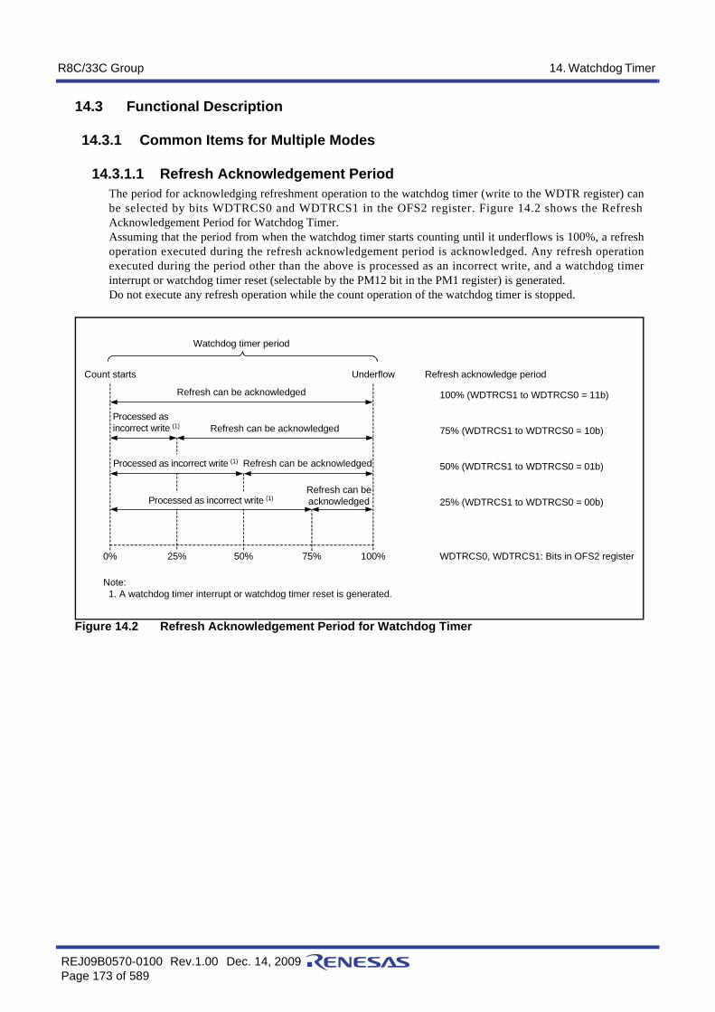
R8C/33C Group 14. Watchdog Timer
REJ09B0570-0100 Rev.1.00 Dec. 14, 2009Page 173 of 589
14.3 Functional Description
14.3.1 Common Items for Multiple Modes
14.3.1.1 Refresh Acknowledgement PeriodThe period for acknowledging refreshment operation to the watchdog timer (write to the WDTR register) canbe selected by bits WDTRCS0 and WDTRCS1 in the OFS2 register. Figure 14.2 shows the RefreshAcknowledgement Period for Watchdog Timer.Assuming that the period from when the watchdog timer starts counting until it underflows is 100%, a refreshoperation executed during the refresh acknowledgement period is acknowledged. Any refresh operationexecuted during the period other than the above is processed as an incorrect write, and a watchdog timerinterrupt or watchdog timer reset (selectable by the PM12 bit in the PM1 register) is generated.Do not execute any refresh operation while the count operation of the watchdog timer is stopped.
Figure 14.2 Refresh Acknowledgement Period for Watchdog Timer
Count starts
Note: 1. A watchdog timer interrupt or watchdog timer reset is generated.
Watchdog timer period
Underflow
0%
Refresh can be acknowledged
Refresh can be acknowledged
Refresh can be acknowledged
Processed as incorrect write (1)Refresh can beacknowledged
Processed asincorrect write (1)
Processed as incorrect write (1)
25% 50% 75% 100%
Refresh acknowledge period
100% (WDTRCS1 to WDTRCS0 = 11b)
75% (WDTRCS1 to WDTRCS0 = 10b)
50% (WDTRCS1 to WDTRCS0 = 01b)
25% (WDTRCS1 to WDTRCS0 = 00b)
WDTRCS0, WDTRCS1: Bits in OFS2 register

R8C/33C Group 14. Watchdog Timer
REJ09B0570-0100 Rev.1.00 Dec. 14, 2009Page 174 of 589
14.3.2 Count Source Protection Mode DisabledThe count source for the watchdog timer is the CPU clock when count source protection mode is disabled.Table 14.2 lists the Watchdog Timer Specifications (Count Source Protection Mode Disabled).
Notes:1. The watchdog timer is initialized when 00h and then FFh is written to the WDTR register. The
prescaler is initialized after a reset. This may cause some errors due to the prescaler during thewatchdog timer period.
2. The WDTON bit cannot be changed by a program. To set this bit, write 0 to bit 0 of address 0FFFFhwith a flash programmer.
3. Write the WDTR register during the count operation of the watchdog timer.
Table 14.2 Watchdog Timer Specifications (Count Source Protection Mode Disabled)Item Specification
Count source CPU clockCount operation DecrementPeriod Division ratio of prescaler (n) × count value of watchdog timer (m) (1)
CPU clock
n: 16 or 128 (selected by the WDTC7 bit in the WDTC register), or 2 when selecting the low-speed clock (CM07 bit in CM0 register = 1)
m: Value set by bits WDTUFS0 and WDTUFS1 in the OFS2 registerExample:The period is approximately 13.1 ms when:- The CPU clock frequency is set to 20 MHz.- The prescaler is divided by 16.- Bits WDTUFS1 to WDTUFS0 are set to 11b (3FFFh).
Watchdog timerinitialization conditions
• Reset• Write 00h and then FFh to the WDTR register. (3)
• UnderflowCount start conditions The operation of the watchdog timer after a reset is selected by
the WDTON bit (2) in the OFS register (address 0FFFFh).• When the WDTON bit is set to 1 (watchdog timer is stopped after reset).
The watchdog timer and prescaler are stopped after a reset and start counting when the WDTS register is written to.
• When the WDTON bit is set to 0 (watchdog timer starts automatically after reset).The watchdog timer and prescaler start counting automatically after a reset.
Count stop condition Stop mode, wait mode (Count resumes from the retained value after exiting.)Operations at underflow • When the PM12 bit in the PM1 register is set to 0.
Watchdog timer interrupt• When the PM12 bit in the PM1 register is set to 1.
Watchdog timer reset (refer to 5.5 Watchdog Timer Reset)

R8C/33C Group 14. Watchdog Timer
REJ09B0570-0100 Rev.1.00 Dec. 14, 2009Page 175 of 589
14.3.3 Count Source Protection Mode EnabledThe count source for the watchdog timer is the low-speed on-chip oscillator clock for the watchdog timer whencount source protection mode is enabled. If the CPU clock stops when a program is out of control, the clock canstill be supplied to the watchdog timer.Table 14.3 lists the Watchdog Timer Specifications (Count Source Protection Mode Enabled).
Notes:1. The WDTON bit cannot be changed by a program. To set this bit, write 0 to bit 0 of address 0FFFFh
with a flash programmer.2. Even if 0 is written to the CSPROINI bit in the OFS register, the CSPRO bit is set to 1. The
CSPROINI bit cannot be changed by a program. To set this bit, write 0 to bit 7 of address 0FFFFhwith a flash programmer.
3. Write the WDTR register during the count operation of the watchdog timer.
Table 14.3 Watchdog Timer Specifications (Count Source Protection Mode Enabled)Item Specification
Count source Low-speed on-chip oscillator clockCount operation DecrementPeriod Count value of watchdog timer (m)
Low-speed on-chip oscillator clock for the watchdog timer
m: Value set by bits WDTUFS0 and WDTUFS1 in the OFS2 registerExample: The period is approximately 8.2 ms when:- The on-chip oscillator clock for the watchdog timer is set to 125 kHz.- Bits WDTUFS1 to WDTUFS0 are set to 00b (03FFh).
Watchdog timerinitialization conditions
• Reset• Write 00h and then FFh to the WDTR register. (3)
• UnderflowCount start conditions The operation of the watchdog timer after a reset is selected by
the WDTON bit (1) in the OFS register (address 0FFFFh).• When the WDTON bit is set to 1 (watchdog timer is stopped after reset).
The watchdog timer and prescaler are stopped after a reset and start counting when the WDTS register is written to.
• When the WDTON bit is set to 0 (watchdog timer starts automatically after reset).The watchdog timer and prescaler start counting automatically after a reset.
Count stop condition None (Count does not stop even in wait mode and stop mode once it starts.)Operation at underflow Watchdog timer reset (Refer to 5.5 Watchdog Timer Reset.)Registers, bits • When the CSPPRO bit in the CSPR register is set to 1 (count source
protection mode enabled) (2), the following are set automatically:- The low-speed on-chip oscillator for the watchdog timer is on.- The PM12 bit in the PM1 register is set to 1 (watchdog timer reset when the
watchdog timer underflows).

R8C/33C Group 15. DTC
REJ09B0570-0100 Rev.1.00 Dec. 14, 2009Page 176 of 589
15. DTCThe DTC (data transfer controller) is a function that transfers data between the SFR and on-chip memory without usingthe CPU. This chip incorporates one DTC channel. The DTC is activated by a peripheral function interrupt to performdata transfers. The DTC and CPU use the same bus, and the DTC takes priority over the CPU in using the bus. To control DTC data transfers, control data comprised of a transfer source address, a transfer destination address, andoperating modes are allocated in the DTC control data area. Each time the DTC is activated, the DTC reads controldata to perform data transfers.
15.1 OverviewTable 15.1 shows the DTC Specifications.
i = 0 to 3, 5, 6, j = 0 to 23
Table 15.1 DTC SpecificationsItem Specification
Activation sources 23 sourcesAllocatable control data 24 setsAddress space which can be transferred 64 Kbytes (00000h to 0FFFFh)Maximum number of transfer times
Normal mode 256 timesRepeat mode 255 times
Maximum size of block to be transferred
Normal mode 256 bytesRepeat mode 255 bytes
Unit of transfers ByteTransfer mode Normal mode Transfers end on completion of the transfer causing the DTCCTj
register value to change from 1 to 0.Repeat mode On completion of the transfer causing the DTCCTj register value to
change from 1 to 0, the repeat area address is initialized and the DTRLDj register value is reloaded to the DTCCTj register to continue transfers.
Address control Normal mode Fixed or incrementedRepeat mode Addresses of the area not selected as the repeat area are fixed or
incremented.Priority of activation sources Refer to Table 15.5 DTC Activation Sources and DTC Vector
Addresses.Interrupt request Normal mode When the data transfer causing the DTCCTj register value to change
from 1 to 0 is performed, the activation source interrupt request is generated for the CPU, and interrupt handling is performed on completion of the data transfer.
Repeat mode When the data transfer causing the DTCCTj register value to change from 1 to 0 is performed while the RPTINT bit in the DTCCRj register is 1 (interrupt generation enabled), the activation source interrupt request is generated for the CPU, and interrupt handling is performed on completion of the transfer.
Transfer start When bits DTCENi0 to DTCENi7 in the DTCENi registers are 1 (activation enabled), data transfer is started each time the corresponding DTC activation sources are generated.
Transfer stop Normal mode • When bits DTCENi0 to DTCENi7 are set to 0 (activation disabled).• When the data transfer causing the DTCCTj register value to
change from 1 to 0 is completed.Repeat mode • When bits DTCENi0 to DTCENi7 are set to 0 (activation disabled).
• When the data transfer causing the DTCCTj register value to change from 1 to 0 is completed while the RPTINT bit is 1 (interrupt generation enabled).

R8C/33C Group 15. DTC
REJ09B0570-0100 Rev.1.00 Dec. 14, 2009Page 177 of 589
Figure 15.1 DTC Block Diagram
15.2 RegistersWhen the DTC is activated, control data (DTCCRj, DTBLSj, DTCCTj, DTRLDj, DTSARj, and DTDARj, j = 0 to23) allocated in the control data area is read, and then transferred to the control registers (DTCCR, DTBLS,DTCCT, DTRLD, DTSAR, and DTDAR) in the DTC. On completion of the DTC data transfer, the contents of theDTC control registers are written back to the control data area.
Each DTCCR, DTBLS, DTCCT, DTRLD, DTSAR, and DTDAR register cannot be directly read or written to.DTCCRj, DTBLSj, DTCCTj, DTRLDj, DTSARj, and DTDARj are allocated as control data at addresses from2C40h to 2CFFh in the DTC control data area, and can be directly accessed. Also, registers DTCTL and DTCENi (i = 0 to 3, 5, 6) can be directly accessed.
DTCENi(i = 0 to 3, 5, 6)
Interrupt controller
Per
iphe
ral i
nter
rupt
requ
est
Con
trol c
ircui
t DTCCR
DTBLS
DTCCT
DTRLD
DTSAR
DTDAR
DTC activationrequest
Peripheral interruptrequest
Inte
rnal
bus
CPU
Bus interface
RO
M
RA
M
Per
iphe
ral
func
tions
DTCCR: DTC control registerDTBLS: DTC block size registerDTCCT: DTC transfer count registerDTRLD: DTC transfer count reload registerDTSAR: DTC source address registerDTDAR: DTC destination address registerDTCTL: DTC activation control registerDTCEN0 to DTCEN6:
DTC activation enable registers 0 to 6
Peripheral bus
DTCTL

R8C/33C Group 15. DTC
REJ09B0570-0100 Rev.1.00 Dec. 14, 2009Page 178 of 589
15.2.1 DTC Control Register j (DTCCRj) (j = 0 to 23)
Notes:1. This bit is valid when the MODE bit is 1 (repeat mode).2. Settings of bits SAMOD and DAMOD are invalid for the repeat area.3. Set the CHNE bit in the DTCCR23 register to 0 (chain transfers disabled).
15.2.2 DTC Block Size Register j (DTBLSj) (j = 0 to 23)
Note:1. When the DTBLS register is set to 00h, the block size is 256 bytes.
Address Refer to Table 15.4 Control Data Allocation Addresses.Bit b7 b6 b5 b4 b3 b2 b1 b0
Symbol — — RPTINT CHNE DAMOD SAMOD RPTSEL MODEAfter Reset X X X X X X X X
Bit Symbol Bit Name Function R/Wb0 MODE Transfer mode select bit 0: Normal mode
1: Repeat modeR/W
b1 RPTSEL Repeat area select bit (1) 0: Transfer destination is the repeat area.1: Transfer source is the repeat area.
R/W
b2 SAMOD Source address control bit (2) 0: Fixed1: Incremented
R/W
b3 DAMOD Destination address control bit (2) 0: Fixed1: Incremented
R/W
b4 CHNE Chain transfer enable bit (3) 0: Chain transfers disabled1: Chain transfers enabled
R/W
b5 RPTINT Repeat mode interrupt enable bit (1) 0: Interrupt generation disabled1: Interrupt generation enabled
R/W
b6 — Reserved bits Set to 0. R/Wb7 —
Address Refer to Table 15.4 Control Data Allocation Addresses.Bit b7 b6 b5 b4 b3 b2 b1 b0
Symbol — — — — — — — —After Reset X X X X X X X X
Bit Function Setting Range R/Wb7 to b0 These bits specify the size of the data block to be transferred by one
activation.00h to FFh (1) R/W

R8C/33C Group 15. DTC
REJ09B0570-0100 Rev.1.00 Dec. 14, 2009Page 179 of 589
15.2.3 DTC Transfer Count Register j (DTCCTj) (j = 0 to 23)
Note:1. When the DTCCT register is set to 00h, the number of transfer times is 256. Each time the DTC is activated, the
DTCCT register is decremented by 1.
15.2.4 DTC Transfer Count Reload Register j (DTRLDj) (j = 0 to 23)
Note:1. Set the initial value for the DTCCT register.
15.2.5 DTC Source Address Register j (DTSARj) (j = 0 to 23)
15.2.6 DTC Destination Address Register j (DTDARj) (j = 0 to 23)
Address Refer to Table 15.4 Control Data Allocation Addresses.Bit b7 b6 b5 b4 b3 b2 b1 b0
Symbol — — — — — — — —After Reset X X X X X X X X
Bit Function Setting Range R/Wb7 to b0 These bits specify the number of times of DTC data transfers. 00h to FFh (1) R/W
Address Refer to Table 15.4 Control Data Allocation Addresses.Bit b7 b6 b5 b4 b3 b2 b1 b0
Symbol — — — — — — — —After Reset X X X X X X X X
Bit Function Setting Range R/Wb7 to b0 This register value is reloaded to the DTCCT register in repeat mode. 00h to FFh (1) R/W
Address Refer to Table 15.4 Control Data Allocation Addresses.Bit b7 b6 b5 b4 b3 b2 b1 b0
Symbol — — — — — — — —After Reset X X X X X X X X
Bit b15 b14 b13 b12 b11 b10 b9 b8Symbol — — — — — — — —
After Reset X X X X X X X X
Bit Function Setting Range R/Wb15 to b0 These bits specify a transfer source address for data transfer. 0000h to FFFFh R/W
Address Refer to Table 15.4 Control Data Allocation Addresses.Bit b7 b6 b5 b4 b3 b2 b1 b0
Symbol — — — — — — — —After Reset X X X X X X X X
Bit b15 b14 b13 b12 b11 b10 b9 b8Symbol — — — — — — — —
After Reset X X X X X X X X
Bit Function Setting Range R/Wb15 to b0 These bits specify a transfer destination address for data transfer. 0000h to FFFFh R/W

R8C/33C Group 15. DTC
REJ09B0570-0100 Rev.1.00 Dec. 14, 2009Page 180 of 589
15.2.7 DTC Activation Enable Register i (DTCENi) (i = 0 to 3, 5, 6)
i = 0 to 3, 5, 6Note:
1. For the operation of this bit, refer to 15.3.7 Interrupt Sources.
The DTCENi registers enable/disable DTC activation by interrupt sources. Table 15.2 shows Correspondencesbetween Bits DTCENi0 to DTCENi7 (i = 0 to 3, 5, 6) and Interrupt Sources.
Address 0088h (DTCEN0), 0089h (DTCEN1), 008Ah (DTCEN2), 008Bh (DTCEN3), 008Dh (DTCEN5), 008Eh (DTCEN6)
Bit b7 b6 b5 b4 b3 b2 b1 b0Symbol DTCENi7 DTCENi6 DTCENi5 DTCENi4 DTCENi3 DTCENi2 DTCENi1 DTCENi0
After Reset 0 0 0 0 0 0 0 0
Bit Symbol Bit Name Function R/Wb0 DTCENi0 DTC activation enable bit (1) 0: Activation disabled
1: Activation enabledR/W
b1 DTCENi1 R/Wb2 DTCENi2 R/Wb3 DTCENi3 R/Wb4 DTCENi4 R/Wb5 DTCENi5 R/Wb6 DTCENi6 R/Wb7 DTCENi7 R/W
Table 15.2 Correspondences between Bits DTCENi0 to DTCENi7 (i = 0 to 3, 5, 6) and Interrupt Sources
Register DTCENi7 Bit
DTCENi6 Bit
DTCENi5 Bit
DTCENi4 Bit
DTCENi3 Bit
DTCENi2 Bit
DTCENi1 Bit
DTCENi0 Bit
DTCEN0 INT0 INT1 — INT3 — — — —
DTCEN1 Key input A/D conversion
UART0 reception
UART0 transmission
UART1 reception
UART1 transmission
UART2 reception
UART2 transmission
DTCEN2SSU/I2C bus receive data
full
SSU/I2C bus transmit
data empty
Voltage Monitor 2
Voltage Monitor 1 — —
Timer RC input-
capture/compare-match A
Timer RC input-
capture/compare-match B
DTCEN3
Timer RCinput-
capture/compare-match C
Timer RCinput-
capture/compare-match D
— — — — — —
DTCEN5 — — Timer RE — — — — —
DTCEN6 — Timer RA — Timer RB Flash ready status — — —

R8C/33C Group 15. DTC
REJ09B0570-0100 Rev.1.00 Dec. 14, 2009Page 181 of 589
15.2.8 DTC Activation Control Register (DTCTL)
Note:1. This bit is set to 0 when the read result is 1 and 0 is written to the same bit. This bit remains
unchanged even if the read result is 0 and 0 is written to the same bit. This bit remains unchanged if1 is written to it.
The DTCTL register controls DTC activation when a non-maskable interrupt (an interrupt by the watchdogtimer, oscillation stop detection, voltage monitor 1, or voltage monitor 2) is generated.
NMIF Bit (Non-Maskable Interrupt Generation Bit)The NMIF bit is set to 1 when a watchdog timer interrupt, an oscillation stop detection interrupt, a voltagemonitor 1 interrupt, or a voltage monitor 2 interrupt is generated.When the NMIF bit is 1, the DTC is not activated even if the interrupt which enables DTC activation isgenerated. If the NMIF bit is changed to 1 during DTC transfer, the transfer is continued until it is completed.
When an interrupt source is the watchdog timer, wait for the following cycles before writing 0 to the NMIF bit:If the WDTC7 bit in the WDTC register is set to 0 (divide-by-16 using the prescaler), wait for 16 cycles of theCPU clock after the interrupt source is generated.If the WDTC7 bit is set to 1 (divide-by-128 using the prescaler), wait for 128 cycles of the CPU clock after theinterrupt source is generated. When an interrupt source is oscillation stop detection, set to the OCD1 bit in the OCD register to 0 (oscillationstop detection interrupt disabled) before writing 0 to the NMIF bit.
Address 0080hBit b7 b6 b5 b4 b3 b2 b1 b0
Symbol — — — — — — NMIF —After Reset 0 0 0 0 0 0 0 0
Bit Symbol Bit Name Function R/Wb0 — Reserved bit Set to 0. R/Wb1 NMIF Non-maskable interrupt generation
bit (1)0: Non-maskable interrupts not generated1: Non-maskable interrupts generated
R/W
b2 — Nothing is assigned. If necessary, set to 0. When read, the content is 0. —b3 —b4 —b5 —b6 —b7 —
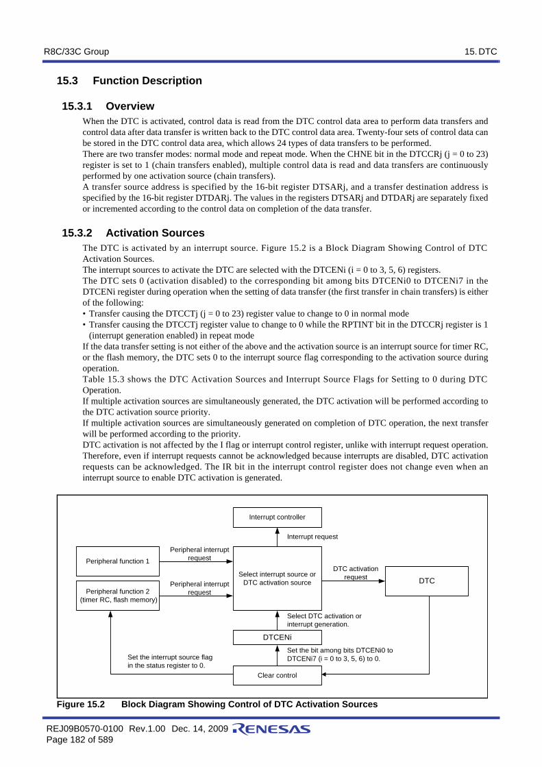
R8C/33C Group 15. DTC
REJ09B0570-0100 Rev.1.00 Dec. 14, 2009Page 182 of 589
15.3 Function Description
15.3.1 OverviewWhen the DTC is activated, control data is read from the DTC control data area to perform data transfers andcontrol data after data transfer is written back to the DTC control data area. Twenty-four sets of control data canbe stored in the DTC control data area, which allows 24 types of data transfers to be performed.There are two transfer modes: normal mode and repeat mode. When the CHNE bit in the DTCCRj (j = 0 to 23)register is set to 1 (chain transfers enabled), multiple control data is read and data transfers are continuouslyperformed by one activation source (chain transfers).A transfer source address is specified by the 16-bit register DTSARj, and a transfer destination address isspecified by the 16-bit register DTDARj. The values in the registers DTSARj and DTDARj are separately fixedor incremented according to the control data on completion of the data transfer.
15.3.2 Activation SourcesThe DTC is activated by an interrupt source. Figure 15.2 is a Block Diagram Showing Control of DTCActivation Sources.The interrupt sources to activate the DTC are selected with the DTCENi (i = 0 to 3, 5, 6) registers.The DTC sets 0 (activation disabled) to the corresponding bit among bits DTCENi0 to DTCENi7 in theDTCENi register during operation when the setting of data transfer (the first transfer in chain transfers) is eitherof the following: • Transfer causing the DTCCTj (j = 0 to 23) register value to change to 0 in normal mode• Transfer causing the DTCCTj register value to change to 0 while the RPTINT bit in the DTCCRj register is 1
(interrupt generation enabled) in repeat modeIf the data transfer setting is not either of the above and the activation source is an interrupt source for timer RC,or the flash memory, the DTC sets 0 to the interrupt source flag corresponding to the activation source duringoperation. Table 15.3 shows the DTC Activation Sources and Interrupt Source Flags for Setting to 0 during DTCOperation.If multiple activation sources are simultaneously generated, the DTC activation will be performed according tothe DTC activation source priority.If multiple activation sources are simultaneously generated on completion of DTC operation, the next transferwill be performed according to the priority.DTC activation is not affected by the I flag or interrupt control register, unlike with interrupt request operation.Therefore, even if interrupt requests cannot be acknowledged because interrupts are disabled, DTC activationrequests can be acknowledged. The IR bit in the interrupt control register does not change even when aninterrupt source to enable DTC activation is generated.
Figure 15.2 Block Diagram Showing Control of DTC Activation Sources
Interrupt controller
Select interrupt source orDTC activation source
DTCENi
Clear control
Peripheral function 1
Peripheral function 2 (timer RC, flash memory)
DTC
Interrupt request
Peripheral interruptrequest
Peripheral interruptrequest
DTC activationrequest
Select DTC activation orinterrupt generation.
Set the bit among bits DTCENi0 toDTCENi7 (i = 0 to 3, 5, 6) to 0.Set the interrupt source flag
in the status register to 0.
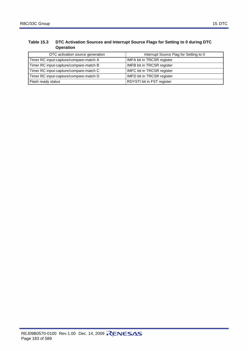
R8C/33C Group 15. DTC
REJ09B0570-0100 Rev.1.00 Dec. 14, 2009Page 183 of 589
Table 15.3 DTC Activation Sources and Interrupt Source Flags for Setting to 0 during DTC Operation
DTC activation source generation Interrupt Source Flag for Setting to 0Timer RC input-capture/compare-match A IMFA bit in TRCSR registerTimer RC input-capture/compare-match B IMFB bit in TRCSR registerTimer RC input-capture/compare-match C IMFC bit in TRCSR registerTimer RC input-capture/compare-match D IMFD bit in TRCSR registerFlash ready status RDYSTI bit in FST register

R8C/33C Group 15. DTC
REJ09B0570-0100 Rev.1.00 Dec. 14, 2009Page 184 of 589
15.3.3 Control Data Allocation and DTC Vector TableControl data is allocated in the order: Registers DTCCRj, DTBLSj, DTCCTj, DTRLDj, DTSARj, and DTDARj(j = 0 to 23). Table 15.4 shows the Control Data Allocation Addresses.
j = 0 to 23
Table 15.4 Control Data Allocation Addresses
Register Symbol
Control Data No. Address DTCCRj
RegisterDTBLSjRegister
DTCCTjRegister
DTRLDjRegister
DTSARjRegister (Lower 8 Bits)
DTSARjRegister (Higher 8 Bits)
DTDARjRegister (Lower 8 Bits)
DTDARjRegister (Higher8 Bits)
DTCD0 Control Data 0
2C40h to 2C47h 2C40h 2C41h 2C42h 2C43h 2C44h 2C45h 2C46h 2C47h
DTCD1 Control Data 1
2C48h to 2C4Fh 2C48h 2C49h 2C4Ah 2C4Bh 2C4Ch 2C4Dh 2C4Eh 2C4Fh
DTCD2 Control Data 2
2C50h to 2C57h 2C50h 2C51h 2C52h 2C53h 2C54h 2C55h 2C56h 2C57h
DTCD3 Control Data 3
2C58h to 2C5Fh 2C58h 2C59h 2C5Ah 2C5Bh 2C5Ch 2C5Dh 2C5Eh 2C5Fh
DTCD4 Control Data 4
2C60h to 2C67h 2C60h 2C61h 2C62h 2C63h 2C64h 2C65h 2C66h 2C67h
DTCD5 Control Data 5
2C68h to 2C6Fh 2C68h 2C69h 2C6Ah 2C6Bh 2C6Ch 2C6Dh 2C6Eh 2C6Fh
DTCD6 Control Data 6
2C70h to 2C77h 2C70h 2C71h 2C72h 2C73h 2C74h 2C75h 2C76h 2C77h
DTCD7 Control Data 7
2C78h to 2C7Fh 2C78h 2C79h 2C7Ah 2C7Bh 2C7Ch 2C7Dh 2C7Eh 2C7Fh
DTCD8 Control Data 8
2C80h to 2C87h 2C80h 2C81h 2C82h 2C83h 2C84h 2C85h 2C86h 2C87h
DTCD9 Control Data 9
2C88h to 2C8Fh 2C88h 2C89h 2C8Ah 2C8Bh 2C8Ch 2C8Dh 2C8Eh 2C8Fh
DTCD10 Control Data 10
2C90h to 2C97h 2C90h 2C91h 2C92h 2C93h 2C94h 2C95h 2C96h 2C97h
DTCD11 Control Data 11
2C98h to 2C9Fh 2C98h 2C99h 2C9Ah 2C9Bh 2C9Ch 2C9Dh 2C9Eh 2C9Fh
DTCD12 Control Data 12
2CA0h to 2CA7h 2CA0h 2CA1h 2CA2h 2CA3h 2CA4h 2CA5h 2CA6h 2CA7h
DTCD13 Control Data 13
2CA8h to 2CAFh 2CA8h 2CA9h 2CAAh 2CABh 2CACh 2CADh 2CAEh 2CAFh
DTCD14 Control Data 14
2CB0h to 2CB7h 2CB0h 2CB1h 2CB2h 2CB3h 2CB4h 2CB5h 2CB6h 2CB7h
DTCD15 Control Data 15
2CB8h to 2CBFh 2CB8h 2CB9h 2CBAh 2CBBh 2CBCh 2CBDh 2CBEh 2CBFh
DTCD16 Control Data 16
2CC0h to 2CC7h 2CC0h 2CC1h 2CC2h 2CC3h 2CC4h 2CC5h 2CC6h 2CC7h
DTCD17 Control Data 17
2CC8h to 2CCFh 2CC8h 2CC9h 2CCAh 2CCBh 2CCCh 2CCDh 2CCEh 2CCFh
DTCD18 Control Data 18
2CD0h to 2CD7h 2CD0h 2CD1h 2CD2h 2CD3h 2CD4h 2CD5h 2CD6h 2CD7h
DTCD19 Control Data 19
2CD8h to 2CDFh 2CD8h 2CD9h 2CDAh 2CDBh 2CDCh 2CDDh 2CDEh 2CDFh
DTCD20 Control Data 20
2CE0h to 2CE7h 2CE0h 2CE1h 2CE2h 2CE3h 2CE4h 2CE5h 2CE6h 2CE7h
DTCD21 Control Data 21
2CE8h to 2CEFh 2CE8h 2CE9h 2CEAh 2CEBh 2CECh 2CEDh 2CEEh 2CEFh
DTCD22 Control Data 22
2CF0h to 2CF7h 2CF0h 2CF1h 2CF2h 2CF3h 2CF4h 2CF5h 2CF6h 2CF7h
DTCD23 Control Data 23
2CF8h to 2CFFh 2CF8h 2CF9h 2CFAh 2CFBh 2CFCh 2CFDh 2CFEh 2CFFh

R8C/33C Group 15. DTC
REJ09B0570-0100 Rev.1.00 Dec. 14, 2009Page 185 of 589
When the DTC is activated, one control data is selected according to the data read from the vector table whichhas been assigned to each activation source, and the selected control data is read from the DTC control dataarea.Table 15.5 shows the DTC Activation Sources and DTC Vector Addresses. A one-byte vector table area isassigned to each activation source and one value from 00000000b to 00010111b (control data numbers in Table15.4) is stored in each area to select one of the 24 control data sets.Figures 15.3 to 15.7 show the DTC Internal Operation Flowchart.
Table 15.5 DTC Activation Sources and DTC Vector AddressesInterrupt Request Source Interrupt Name Source No. DTC Vector Address Priority
External input INT0 0 2C00h High
INT1 1 2C01h
(Reserved) 2 2C02h
INT3 3 2C03h
(Reserved) 4 2C04hKey input Key input 8 2C08hA/D A/D conversion 9 2C09hUART0 UART0 reception 10 2C0Ah
UART0 transmission 11 2C0BhUART1 UART1 reception 12 2C0Ch
UART1 transmission 13 2C0DhUART2 UART2 reception 14 2C0Eh
UART2 transmission 15 2C0FhSSU/I2C bus Receive data full 16 2C10h
Transmit data empty 17 2C11hVoltage detection circuit Voltage monitor 2 18 2C12h
Voltage monitor 1 19 2C13hTimer RC Input-capture/compare-match A 22 2C16h
Input-capture/compare-match B 23 2C17hInput-capture/compare-match C 24 2C18hInput-capture/compare-match D 25 2C19h
(Reserved) — 26 2C1Ah— 27 2C1Bh— 28 2C1Ch— 29 2C1Dh— 30 2C1Eh— 31 2C1Fh— 32 2C20h— 33 2C21h
Timer RE Timer RE 42 2C2AhTimer RA Timer RA 49 2C31hTimer RB Timer RB 51 2C33hFlash memory Flash ready status 52 2C34h Low

R8C/33C Group 15. DTC
REJ09B0570-0100 Rev.1.00 Dec. 14, 2009Page 186 of 589
Figure 15.3 DTC Internal Operation Flowchart When DTC Activation Source is not SSU/I2C bus, Timer RC, or Flash Memory Interrupt Source
Figure 15.4 DTC Internal Operation Flowchart When DTC Activation Source is Timer RC Interrupt Source
DTC activation sourcegeneration
NMIF = 1?
Read DTC vector
Read control data
Transfer data
Write back control data
CHNE=1?
Branch 10 is written to the bit among bits DTCENi0 to DTCENi7 and an interrupt request is generatedwhen transfer is either of the following:- Transfer causing the DTCCTj (j = 0 to 23) register value to change from 1 to 0 in normal mode- Transfer causing the DTCCTj register value to change from 1 to 0 while the RPTINT bit is 1 in
repeat mode
Yes
No
DTCENi0 to DTCENi7: Bits in DTCENi (i = 0 to 3, 5, 6) registersRPTINT, CHNE: Bits in DTCCRj registersNMIF: Bit in DTCTL register
Branch 1
End
No
Yes
Yes
Read control data
Transfer data
Write back control data
CHNE=1?
No
Write 0 to the bit amongDTCENi0 to DTCENi7
Generate an interrupt requestfor the CPU
Transfer data
Write back control data
CHNE=1?Yes
No
Interrupt handling
Read control data
Transfer data
Write back control data
CHNE=1?Yes
No
DTC activation sourcegeneration
NMIF = 1?
Read DTC vector
Read control data
Write 0 to the interrupt sourceflag in the status register
Transfer data
Branch 10 is written to the bit among bits DTCENi0 to DTCENi7 and an interrupt request is generatedwhen transfer is either of the following:- Transfer causing the DTCCTj (j = 0 to 23) register value to change from 1 to 0 in normal mode- Transfer causing the DTCCTj register value to change from 1 to 0 while the RPTINT bit is 1 in
repeat mode
Yes
DTCENi0 to DTCENi7: Bits in DTCENi (i = 0 to 3, 5, 6) registersRPTINT, CHNE: Bits in DTCCRj registersNMIF: Bit in DTCTL register
Branch 1
No
Yes
Read control data
Transfer data
Write back control data
CHNE=1?
No
Write 0 to the bit amongDTCENi0 to DTCENi7
Generate an interrupt requestfor the CPU
Transfer data
Write back control data
CHNE=1?Yes
No
Interrupt handling
Read control data
Transfer data
Write back control data
CHNE=1?Yes
No
CHNE=1?
No
End
Yes
Write back control data

R8C/33C Group 15. DTC
REJ09B0570-0100 Rev.1.00 Dec. 14, 2009Page 187 of 589
Figure 15.5 DTC Internal Operation Flowchart When DTC Activation Source is SSU/I2C bus Receive Data Full
Figure 15.6 DTC Internal Operation Flowchart When DTC Activation Source is SSU/I2C bus Transmit Data Empty
DTC activation source generation
NMIF = 1?
Read DTC vector
Read control data
Transfer data(Reading the receive data register
sets the RDRF bit to 0) (1)
Write back control data
CHNE=1?
Branch 10 is written to the bit among bits DTCENi0 to DTCENi7 and an interrupt request is generatedwhen transfer is either of the following:- Transfer causing the DTCCTj (j = 0 to 23) register value to change from 1 to 0 in normal mode- Transfer causing the DTCCTj register value to change from 1 to 0 while the RPTINT bit is 1 in
repeat mode
YesNo
DTCENi0 to DTCENi7: Bits in DTCENi (i = 0 to 3, 5, 6) registersRPTINT, CHNE: Bits in DTCCRj registersNMIF: Bit in DTCTL registerRDRF: Bit in SSSR/ICSR register
Branch 1
End
No
Yes
Yes
Read control data
Transfer data(Reading the receive data register
sets the RDRF bit to 0) (1)
Write back control data
CHNE=1?
No
Write 0 to the bit amongDTCENi0 to DTCENi7
Generate an interrupt requestfor the CPU
Transfer data(Reading the receive data register
does not set the RDRF bit to 0)
Write back control data
CHNE=1?Yes
No
Interrupt handling
Read control data
Transfer data(Reading the receive data register
does not set the RDRF bit to 0)
Write back control data
CHNE=1?Yes
No
Note:1. When the DTC activation source is SSU/I2C bus receive data full, the DTC does not set the RDRF bit in the SSSR register/the ICSR register to 0.
Instead, reading the receive data register during DTC data transfer sets the RDRF bit to 0.
DTC activation source generation
NMIF = 1?
Read DTC vector
Read control data
Transfer data(writing the transmit data register
sets the TDRE bit to 0) (1)
Write back control data
CHNE=1?
Branch 10 is written to the bit among bits DTCENi0 to DTCENi7 when transfer is either of the following:- Transfer causing the DTCCTj (j = 0 to 23) register value to change from 1 to 0 in normal mode- Transfer causing the DTCCTj register value to change from 1 to 0 while the RPTINT bit is 1 in
repeat mode
YesNo
DTCENi0 to DTCENi7: Bits in DTCENi (i = 0 to 3, 5, 6) registersRPTINT, CHNE: Bits in DTCCRj registersNMIF: Bit in DTCTL registerTDRE: Bit in SSSR/ICSR register
Branch 1
End
No
Yes
Yes
Read control data
Transfer data(writing the transmit data register
sets the TDRE bit to 0) (1)
Write back control data
CHNE=1?
No
Write 0 to the bit amongDTCENi0 to DTCENi7
Transfer data(writing the transmit data register
sets the TDRE bit to 0) (1)
Write back control data
CHNE=1?Yes
No
Read control data
Transfer data(writing the transmit data register
sets the TDRE bit to 0) (1)
Write back control data
CHNE=1?Yes
No
Note:1. When the DTC activation source is SSU/I2C bus transmit data empty, the DTC does not set the TDRE bit in the SSSR register/the ICSR register to 0.
Instead, writing data to the transmit data register during DTC data transfer sets the TDRE bit to 0.

R8C/33C Group 15. DTC
REJ09B0570-0100 Rev.1.00 Dec. 14, 2009Page 188 of 589
Figure 15.7 DTC Internal Operation Flowchart When DTC Activation Source is Flash ready status
DTC activation sourcegeneration
NMIF = 1?
Read DTC vector
Read control data
Write 0 to the interrupt sourceflag in the status register
Transfer data
Branch 10 is written to the bit among bits DTCENi0 to DTCENi7 when transfer is either of the following:- Transfer causing the DTCCTj (j = 0 to 23) register value to change from 1 to 0 in normal mode- Transfer causing the DTCCTj register value to change from 1 to 0 while the RPTINT bit is 1 in
repeat mode
Yes
DTCENi0 to DTCENi7: Bits in DTCENi (i = 0 to 3, 5, 6) registersRPTINT, CHNE: Bits in DTCCRj registerNMIF: Bit in DTCTL register
Branch 1
No
Yes
Read control data
Transfer data
Write back control data
CHNE=1?
No
Write 0 to the bit amongDTCENi0 to DTCENi7
Write 0 to the interrupt sourceflag in the status register
Transfer data
Write back control data
CHNE=1?Yes
No
Read control data
Transfer data
Write back control data
CHNE=1?Yes
No
CHNE=1?
No
End
Yes
Write back control data

R8C/33C Group 15. DTC
REJ09B0570-0100 Rev.1.00 Dec. 14, 2009Page 189 of 589
15.3.4 Normal ModeOne to 256 bytes of data are transferred by one activation. The number of transfer times can be 1 to 256. Whenthe data transfer causing the DTCCTj (j = 0 to 23) register value to change to 0 is performed, an interruptrequest for the CPU is generated during DTC operation. Table 15.6 shows Register Functions in Normal Mode.Figure 15.8 shows Data Transfers in Normal Mode.
j =0 to 23
Figure 15.8 Data Transfers in Normal Mode
Table 15.6 Register Functions in Normal ModeRegister Symbol Function
DTC block size register j DTBLSj Size of the data block to be transferred by one activationDTC transfer count register j DTCCTj Number of times of data transfersDTC transfer count reload register j
DTRLDj Not used
DTC source address register j DTSARj Data transfer source addressDTC destination address register j
DTDARj Data transfer destination address
SRCTransfer
DST
Transfer source Transfer destination
Size of the data block to be transferredby one activation (N bytes)
DTBLSj = NDTSARj = SRCDTDARj = DST
j = 0 to 23
Bits b3 to b0 inDTCCR register
00X0b01X0b10X0b11X0b
Source addresscontrol
FixedIncremented
FixedIncremented
Destination addresscontrol
FixedFixed
IncrementedIncremented
Source addressafter transfer
SRCSRC+N
SRCSRC+N
Destination addressafter transfer
DSTDST
DST+NDST+N
X: 0 or 1

R8C/33C Group 15. DTC
REJ09B0570-0100 Rev.1.00 Dec. 14, 2009Page 190 of 589
15.3.5 Repeat ModeOne to 255 bytes of data are transferred by one activation. Either of the transfer source or destination should bespecified as the repeat area. The number of transfer times can be 1 to 255. On completion of the specifiednumber of transfer times, the DTCCTj (i =0 to 23) register and the address specified for the repeat area areinitialized to continue transfers. When the data transfer causing the DTCCTj register value to change to 0 isperformed while the RPTINT bit in the DTCCRj register is 1 (interrupt generation enabled), an interrupt requestfor the CPU is generated during DTC operation.The lower 8 bits of the initial value for the repeat area address must be 00h. The size of data to be transferredmust be set to 255 bytes or less before the specified number of transfer times is completed. Table 15.7 shows Register Functions in Repeat Mode.Figure 15.9 shows Data Transfers in Repeat Mode.
j =0 to 23
Figure 15.9 Data Transfers in Repeat Mode
Table 15.7 Register Functions in Repeat ModeRegister Symbol Function
DTC block size register j DTBLSj Size of the data block to be transferred by one activationDTC transfer count register j DTCCTj Number of times of data transfersDTC transfer count reload register j DTRLDj This register value is reloaded to the DTCCT register. (Data
transfer count is initialized.)DTC source address register j DTSARj Data transfer source addressDTC destination address register j DTDARj Data transfer destination address
SRCTransfer
DST
Transfer source Transfer destination
Size of the data block to be transferred byone activation (N bytes)
DTBLSj = NDTCCTj ≠ 1DTSARj = SRCDTDARj = DST
j = 0 to 23
Bits b3 to b0 inDTCCR register
0X11b1X11bX001bX101b
Source addresscontrol
Repeat areaRepeat area
FixedIncremented
Destination addresscontrolFixed
IncrementedRepeat areaRepeat area
Source addressafter transfer
SRC+NSRC+N
SRCSRC+N
Destination addressafter transfer
DSTDST+NDST+NDST+N
DTCCTj register = 1
SRC0/DST0
…
Repeat area
Bits b3 to b0 inDTCCR register
0X11b1X11bX001bX101b
Source addresscontrol
Repeat areaRepeat area
FixedIncremented
Destination addresscontrol
FixedIncrementedRepeat areaRepeat area
Source addressafter transfer
SRC0SRC0SRC
SRC+N
Destination addressafter transfer
DSTDST+NDST0DST0
SRC/DST
Address of the repeat area is initializedafter a transfer.
DTBLSj = NDTCCTj = 1DTSARj = SRCDTDARj = DST
j = 0 to 23
SRC0: Initial source address valueDST0: Initial destination address valueX: 0 or 1
X: 0 or 1
DTCCTj register ≠ 1

R8C/33C Group 15. DTC
REJ09B0570-0100 Rev.1.00 Dec. 14, 2009Page 191 of 589
15.3.6 Chain TransfersWhen the CHNE bit in the DTCCRj (j = 0 to 22) register is 1 (chain transfers enabled), multiple data transferscan be continuously performed by one activation source. Figure 15.10 shows a Flow of Chain Transfers.When the DTC is activated, one control data is selected according to the data read from the DTC vector addresscorresponding to the activation source, and the selected control data is read from the DTC control data area.When the CHNE bit for the control data is 1 (chain transfers enabled), the next control data immediatelyfollowing the current control data is read and transferred after the current transfer is completed. This operationis repeated until the data transfer with the control data for which the CHNE bit is 0 (chain transfers disabled) iscompleted.Set the CHNE bit in the DTCCR23 register to 0 (chain transfers disabled).
Figure 15.10 Flow of Chain Transfers
15.3.7 Interrupt SourcesWhen the data transfer causing the DTCCTj (j = 0 to 23) register value to change to 0 is performed in normalmode, and when the data transfer causing the DTCCTj register value to change to 0 is performed while theRPTINT bit in the DTCCRj register is 1 (interrupt generation enabled) in repeat mode, the interrupt requestcorresponding to the activation source is generated for the CPU during DTC operation. However, no interruptrequest is generated for the CPU when the activation source is SSU/I2C bus transmit data empty or flash readystatus. Interrupt requests for the CPU are affected by the I flag or interrupt control register. In chain transfers, whetherthe interrupt request is generated or not is determined either by the number of transfer times specified for thefirst type of the transfer or the RPTINT bit. When an interrupt request is generated for the CPU, the bit amongbits DTCENi0 to DTCENi7 in the DTCENi (i = 0 to 3, 5, 6) registers corresponding to the activation source areset to 0 (activation disabled).
DTC activation sourcegeneration
Read DTC vector
Read control data 1
Transfer data
Write back control data 1
Read control data 2
Data transfer
Write back control data 2
End of DTC transfers
Control data 1CHNE = 1
Control data 2CHNE = 0
DTC control data area
CHNE: Bit in DTCCRj register
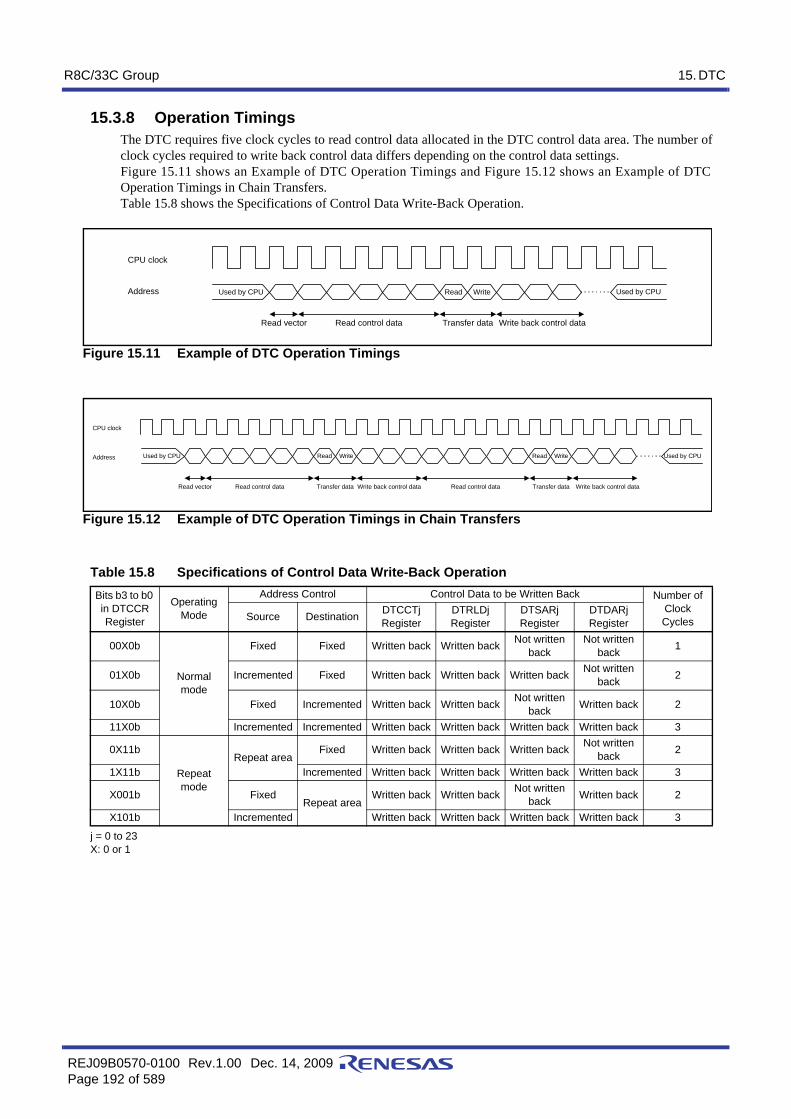
R8C/33C Group 15. DTC
REJ09B0570-0100 Rev.1.00 Dec. 14, 2009Page 192 of 589
15.3.8 Operation TimingsThe DTC requires five clock cycles to read control data allocated in the DTC control data area. The number ofclock cycles required to write back control data differs depending on the control data settings.Figure 15.11 shows an Example of DTC Operation Timings and Figure 15.12 shows an Example of DTCOperation Timings in Chain Transfers.Table 15.8 shows the Specifications of Control Data Write-Back Operation.
Figure 15.11 Example of DTC Operation Timings
Figure 15.12 Example of DTC Operation Timings in Chain Transfers
j = 0 to 23X: 0 or 1
Table 15.8 Specifications of Control Data Write-Back OperationBits b3 to b0 in DTCCR Register
Operating Mode
Address Control Control Data to be Written Back Number of Clock CyclesSource Destination DTCCTj
RegisterDTRLDj Register
DTSARj Register
DTDARj Register
00X0b
Normal mode
Fixed Fixed Written back Written back Not written back
Not written back 1
01X0b Incremented Fixed Written back Written back Written back Not written back 2
10X0b Fixed Incremented Written back Written back Not written back Written back 2
11X0b Incremented Incremented Written back Written back Written back Written back 3
0X11b
Repeat mode
Repeat areaFixed Written back Written back Written back Not written
back 2
1X11b Incremented Written back Written back Written back Written back 3
X001b FixedRepeat area
Written back Written back Not written back Written back 2
X101b Incremented Written back Written back Written back Written back 3
Used by CPU Used by CPU
Read control data Transfer data Write back control data
CPU clock
Address Read Write
Read vector
Used by CPU Read Write Used by CPU
Read control data Transfer data Write back control data Read control data Transfer data Write back control data
CPU clock
Address Read Write
Read vector

R8C/33C Group 15. DTC
REJ09B0570-0100 Rev.1.00 Dec. 14, 2009Page 193 of 589
15.3.9 Number of DTC Execution CyclesTable 15.9 shows the Operations Following DTC Activation and Required Number of Cycles for eachoperation. Table 15.10 shows the Number of Clock Cycles Required for Data Transfers.
Notes:1. For the number of clock cycles required for data read/write, refer to Table 15.10 Number of Clock
Cycles Required for Data Transfers.2. For the number of clock cycles required for control data write-back, refer to Table 15.8
Specifications of Control Data Write-Back Operation.
Data is transferred as described below, when the DTBLSj (j = 0 to 23) register = N,(1) When N = 2n (even), two-byte transfers are performed n times. (2) When N = 2n + 1 (odd), two-byte transfers are performed n times followed by one time of one-byte
transfer.
From Tables 15.9 and 15.10, the total number of required execution cycles can be obtained by the followingformula:
Number of required execution cycles = 1 + Σ[formula A] + 2Σ: Sum of the cycles for the number of transfer times performed by one activation source ([the number oftransfer times for which CHNE is set to 1] + 1)
(1) For N = 2n (even)Formula A = J + n • SK2 + n • SL2
(2) For N = 2n+1 (odd)Formula A = J + n • SK2 + 1 • SK1 + n • SL2 + 1 • SL1J: Number of cycles required to read control data (5 cycles) + number of cycles required to write back control data
To read data from or write data to the register that to be accessed in 16-bit units, set an even value of 2 or greaterto the DTBLSj (j = 0 to 23) register. The DTC performs accesses in 16-bit units.
Table 15.9 Operations Following DTC Activation and Required Number of Cycles
Vector ReadControl Data
Data Read Data Write Internal OperationRead Write-back
1 5 (Note 2) (Note 1) (Note 1) 1
Table 15.10 Number of Clock Cycles Required for Data Transfers
Operation Unit of Transfers
Internal RAM(During DTC Transfers) Internal ROM
(Program ROM)Internal ROM(Data flash)
SFR(Word Access) SFR
(Byte Access)
SFR(DTC control data area)
Even Address
Odd Address
Even Address
Odd Address
Even Address
Odd Address
Data read1-byte SK1 1 1 2 2 2 12-byte SK2 1 2 2 4 2 4 4 1 2
Data write1-byte SL1 1 — — 2 2 12-byte SL2 1 2 — — 2 4 4 1 2

R8C/33C Group 15. DTC
REJ09B0570-0100 Rev.1.00 Dec. 14, 2009Page 194 of 589
15.3.10 DTC Activation Source Acknowledgement and Interrupt Source Flags
15.3.10.1 Interrupt Sources Except for Flash Memory, Timer RC, andSynchronous Serial Communication Unit (SSU)/I2C bus
When the DTC activation source is an interrupt source except for the flash memory, timer RC, or thesynchronous serial communication unit/I2C bus, the same DTC activation source cannot be acknowledged for 8to 12 cycles of the CPU clock after the interrupt source is generated. If an interrupt source is generated when asoftware command is executed, the same DTC activation source cannot be acknowledged for 9 to 16 cycles ofthe CPU clock. If a DTC activation source is generated during DTC operation and acknowledged, the sameDTC activation source cannot be acknowledged for 8 to 12 cycles of the CPU clock on completion of the DTCtransfer immediately before the DTC is activated by the source. When a software command is executed oncompletion of the DTC transfer immediately before the DTC is activated, the same DTC activation sourcecannot be acknowledged for 16 cycles of the CPU clock.
15.3.10.2 Flash MemoryWhen the DTC activation source is flash ready status, even if a flash ready status interrupt request is generated,it is not acknowledged as the DTC activation source after the RDYSTI bit in the FST register is set to 1 (flashready status interrupt request) and before the DTC sets the RDYSTI bit to 0 (no flash ready status interruptrequest). If a flash ready status interrupt request is generated after the DTC sets the RDYSTI bit to 0, the DTCacknowledges it as the activation source. 8 to 12 cycles of the CPU clock are required after the RDYSTI bit isset to 1 and before the DTC sets the interrupt request flag to 0. If a flash ready status interrupt is generated whena software command is executed, 9 to 16 cycles of the CPU clock are required before the DTC sets the interruptsource flag to 0. If a flash ready status interrupt request is generated during DTC operation and acknowledgedas the DTC activation source, the RDYSTI bit is set to 0 after 8 to 12 cycles of the CPU clock on completion ofthe DTC transfer immediately before the DTC is activated by the source. When a software command isexecuted on completion of the DTC transfer immediately before the DTC is activated, the RDYSTI bit is set to0 after 16 cycles of the CPU clock.
15.3.10.3 Timer RCWhen the DTC activation source is an interrupt source for timer RC, even if an input capture/compare matchoccurs, it is not acknowledged as the DTC activation source after the interrupt source flag is set to 1 and beforethe DTC sets the flag to 0. If an input capture/compare match occurs after the DTC sets the interrupt source flagto 0, the DTC acknowledges it as the activation source. 8 to 12 cycles of the CPU clock plus 0.5 to 1.5 cycles ofthe timer operating clock are required after the interrupt source flag is set to 1 and before the DTC sets the flagto 0. If the interrupt request flag is set to 1 when a software command is executed, 9 to 16 cycles of the CPUclock plus 0.5 to 1.5 cycles of the timer operating clock are required before the DTC sets the interrupt sourceflag to 0. If individual DTC activation sources are generated for timer RC during DTC operation andacknowledged, the interrupt source flag is set to 0 after 8 to 12 cycles of the CPU clock plus 0.5 to 1.5 cycles ofthe timer operating clock on completion of the DTC transfer immediately before the DTC is activated by thesource. When a software command is executed on completion of the DTC transfer immediately before the DTCis activated, the interrupt source flag is set to 0 after 16 cycles of the CPU clock plus 0.5 to 1.5 cycles of thetimer operating clock.

R8C/33C Group 15. DTC
REJ09B0570-0100 Rev.1.00 Dec. 14, 2009Page 195 of 589
15.3.10.4 SSU/I2C bus Receive Data FullWhen the DTC activation source is SSU/I2C bus receive data full, read the SSRDR register/the ICDRR registerusing a data transfer. The RDRF bit in the SSSR register/the ICSR register is set to 0 (no data inSSRDR/ICDRR register) by reading the SSRDR register/ the ICDRR register. If an interrupt source for receivedata full is subsequently generated, the DTC acknowledges it as the activation source.
15.3.10.5 SSU/I2C bus Transmit Data EmptyWhen the DTC activation source is SSU/I2C bus transmit data empty, write to the SSTDR register/the ICDRTregister using a data transfer. The TDRE bit in the SSSR register/the ICSR register is set to 0 (data is nottransferred from registers SSTDR/ICDRT to SSTRSR/ICDRS) by writing to the SSTDR register/the ICDRTregister. If an interrupt source for transmit data empty is subsequently generated, the DTC acknowledges it asthe activation source.

R8C/33C Group 15. DTC
REJ09B0570-0100 Rev.1.00 Dec. 14, 2009Page 196 of 589
15.4 Notes on DTC
15.4.1 DTC activation source• Do not generate any DTC activation sources before entering wait mode or during wait mode. • Do not generate any DTC activation sources before entering stop mode or during stop mode.
15.4.2 DTCENi (i = 0 to 3, 5, 6) Registers• Modify bits DTCENi0 to DTCENi7 only while an interrupt request corresponding to the bit is not generated.• When the interrupt source flag in the status register for the peripheral function is 1, do not modify the
corresponding activation source bit among bits DTCENi0 to DTCENi7.• Do not access the DTCENi registers using DTC transfers.
15.4.3 Peripheral Modules• Do not set the status register bit for the peripheral function to 0 using a DTC transfer.• When the DTC activation source is SSU/I2C bus receive data full, read the SSRDR register/the ICDRR
register using a DTC transfer.The RDRF bit in the SSSR register/the ICSR register is set to 0 (no data in SSRDR/ICDRR register) byreading the SSRDR register/the ICDRR register.However, the RDRF bit is not set to 0 by reading the SSRDR register/the ICDRR register when the DTC datatransfer setting is either of the following:- Transfer causing the DTCCTj (j = 0 to 23) register value to change from 1 to 0 in normal mode- Transfer causing the DTCCRj register value to change from 1 to 0 while the RPTINT bit in the DTCCRj
register is 1 (interrupt generation enabled) in repeat mode• When the DTC activation source is SSU/I2C bus transmit data empty, write to the SSTDR register/the ICDRT
register using a DTC transfer. The TDRE bit in the SSSR register/the ICSR register is set to 0 (data is nottransferred from registers SSTDR/ICDRT to SSTRSR/ICDRS) by writing to the SSTDR register/the ICDRTregister.
15.4.4 Interrupt RequestNo interrupt is generated for the CPU during DTC operation in any of the following cases:- When the DTC activation source is SSU/I2C transmit data empty or flash ready status- When performing the data transfer causing the DTCCTj (j = 0 to 23) register value to change to 0 in normal
mode- When performing the data transfer causing the DTCCRj register value to change to 0 while the RPTINT bit in
the DTCCRj register is 1 (interrupt generation enabled) in repeat mode

R8C/33C Group 16. General Overview of Timers
REJ09B0570-0100 Rev.1.00 Dec. 14, 2009Page 197 of 589
16. General Overview of TimersThe MCU has two 8-bit timers with 8-bit prescalers, a 16-bit timer, and a timer with a 4-bit counter and an 8-bitcounter. The two 8-bit timers with 8-bit prescalers are timer RA and timer RB. These timers contain a reload register tostore the default value of the counter. The 16-bit timers are timer RC, and have input capture and output comparefunctions. The 4-bit and 8-bit counters are timer RE, and has an output compare function. All the timers operateindependently. Table 16.1 lists Functional Comparison of Timers.

R8C/33C Group 16. General Overview of Timers
REJ09B0570-0100 Rev.1.00 Dec. 14, 2009Page 198 of 589
Note:1. Rectangular waves are output in these modes. Since the waves are inverted at each overflow, the “H” and “L” level widths of
the pulses are the same.
Table 16.1 Functional Comparison of TimersItem Timer RA Timer RB Timer RC Timer RE
Configuration 8-bit timer with 8-bit prescaler (with reload register)
8-bit timer with 8-bit prescaler (with reload register)
16-bit timer (with input capture and output compare)
4-bit counter8-bit counter
Count Decrement Decrement Increment IncrementCount sources • f1
• f2• f8• fOCO• fC32• fC
• f1• f2• f8• Timer RA underflow
• f1• f2• f4• f8• f32• fOCO40M• fOCO-F• TRCCLK
• f4• f8• f32• fC4
Function Count of the internal count source
Timer mode Timer mode Timer mode (output compare function)
—
Count of the external count source
Event counter mode — Timer mode (output compare function)
—
External pulse width/period measurement
Pulse width measurement mode, pulse period measurement mode
— Timer mode (input capture function; 4 pins)
—
PWM output Pulse output mode (1), Event counter mode (1)
Programmable waveform generation mode
Timer mode (output compare function; 4 pins) (1),PWM mode (3 pins),PWM2 mode (1 pin)
Output compare mode (1)
One-shot waveform output
— Programmable one-shot generation mode, Programmable wait one-shot generation mode
PWM mode (3 pins) —
Three-phase waveforms output
— — — —
Timer Timer mode (only fC32 count)
— — Real-time clock mode
Input pin TRAIO,INT2
INT0 INT0, TRCCLK,TRCTRG, TRCIOA, TRCIOB, TRCIOC, TRCIOD
—
Output pin TRAO,TRAIO
TRBO TRCIOA,TRCIOB, TRCIOC, TRCIOD
TREO
Related interrupt Timer RA interrupt,INT2 interrupt
Timer RB interrupt, INT0 interrupt
Compare match/input capture A to D interrupt, Overflow interrupt, INT0 interrupt
Timer RE interrupt
Timer stop Provided Provided Provided Provided

R8C/33C Group 17. Timer RA
REJ09B0570-0100 Rev.1.00 Dec. 14, 2009Page 199 of 589
17. Timer RATimer RA is an 8-bit timer with an 8-bit prescaler.
17.1 OverviewThe prescaler and timer each consist of a reload register and counter. The reload register and counter are allocated atthe same address, and can be accessed when accessing registers TRAPRE and TRA (refer to Tables 17.2 to 17.6 theSpecifications of Each Mode).The count source for timer RA is the operating clock that regulates the timing of timer operations such as counting andreloading.
Figure 17.1 shows a Timer RA Block Diagram. Table 17.1 lists Pin Configuration of Timer RA.
Timer RA contains the following five operating modes:• Timer mode: The timer counts the internal count source.• Pulse output mode: The timer counts the internal count source and outputs pulses which invert the
polarity by underflow of the timer.• Event counter mode: The timer counts external pulses.• Pulse width measurement mode: The timer measures the pulse width of an external pulse.• Pulse period measurement mode: The timer measures the pulse period of an external pulse.
Figure 17.1 Timer RA Block Diagram
Table 17.1 Pin Configuration of Timer RA
Pin Name Assigned Pin I/O Function
TRAIO P1_5 or P1_7 I/O Function differs according to the mode. Refer to descriptions of individual modes for detailsTRAO P3_7 Output
TCK2 to TCK0 bit
TMOD2 to TMOD0= other than 010b
Counter
Reloadregister
TRAPRE register(prescaler)
Data bus
Timer RA interrupt
Write to TRAMR registerWrite 1 to TSTOP bit
TCSTF, TSTOP: TRACR registerTEDGSEL, TOPCR, TOENA, TIPF1, TIPF0, TIOGT1, TIOGT0: TRAIOC registerTMOD2 to TMOD0, TCK2 to TCK0, TCKCUT: TRAMR register
Toggleflip-flop
Q
Q CLR
CK
TOENA bit
TRAO pin
TCSTF bitTCKCUT bit
TMOD2 to TMOD0= 011b or 100b
TMOD2 to TMOD0= 010b
Polarityswitching
Digitalfilter
Counter
Reloadregister
TRA register(timer)
TIPF1 to TIPF0 bits= 01b= 10bf8
f1
= 11bf32Count control
circle
TMOD2 to TMOD0 = 001bTOPCR bit
Underflow signal
Measurementcompletion signal
TIPF1 to TIPF0 bits= other than 000b
= 00b
TEDGSEL = 1
TEDGSEL = 0
= 000b= 001b
= 011bf2
f8f1
= 010bfOCO
= 100bfC32
Note:1. Bits TRAIOSEL0 and TRAIOSEL1 in the TRASR register are used to select which pin is assigned.
TIOGT1 to TIOGT0 bits
= 01b= 10b
Do not setEvent input always enabled = 00b
Event enabled for “L” period ofTRCIOD (timer RC output)
= 110bfC
TRAIO pin (1)

R8C/33C Group 17. Timer RA
REJ09B0570-0100 Rev.1.00 Dec. 14, 2009Page 200 of 589
17.2 Registers
17.2.1 Timer RA Control Register (TRACR)
Notes:1. Refer to 17.8 Notes on Timer RA for precautions regarding bits TSTART and TCSTF.2. When the TSTOP bit is set to 1, bits TSTART and TCSTF and registers TRAPRE and TRA are set to the values
after a reset.3. Bits TEDGF and TUNDF can be set to 0 by writing 0 to these bits by a program. However, their value remains
unchanged when 1 is written.4. Set to 0 in timer mode, pulse output mode, and event counter mode.
In pulse width measurement mode and pulse period measurement mode, use the MOV instruction to set theTRACR register. If it is necessary to avoid changing the values of bits TEDGF and TUNDF, write 1 to them.
17.2.2 Timer RA I/O Control Register (TRAIOC)
Address 0100hBit b7 b6 b5 b4 b3 b2 b1 b0
Symbol — — TUNDF TEDGF — TSTOP TCSTF TSTARTAfter Reset 0 0 0 0 0 0 0 0
Bit Symbol Bit Name Function R/Wb0 TSTART Timer RA count start bit (1) 0: Count stops
1: Count startsR/W
b1 TCSTF Timer RA count status flag (1) 0: Count stops1: During count
R
b2 TSTOP Timer RA count forcible stop bit (2) When this bit is set to 1, the count is forcibly stopped. When read, its content is 0.
R/W
b3 — Nothing is assigned. If necessary, set to 0. When read, the content is 0. —b4 TEDGF Active edge judgment flag (3, 4) 0: Active edge not received
1: Active edge received (end of measurement period)R/W
b5 TUNDF Timer RA underflow flag (3, 4) 0: No underflow1: Underflow
R/W
b6 — Nothing is assigned. If necessary, set to 0. When read, the content is 0. —b7 —
Address 0101hBit b7 b6 b5 b4 b3 b2 b1 b0
Symbol TIOGT1 TIOGT0 TIPF1 TIPF0 TIOSEL TOENA TOPCR TEDGSELAfter Reset 0 0 0 0 0 0 0 0
Bit Symbol Bit Name Function R/Wb0 TEDGSEL TRAIO polarity switch bit Function varies according to the operating mode. R/Wb1 TOPCR TRAIO output control bit R/Wb2 TOENA TRAO output enable bit R/Wb3 TIOSEL Hardware LIN function select bit R/Wb4 TIPF0 TRAIO input filter select bit R/Wb5 TIPF1 R/Wb6 TIOGT0 TRAIO event input control bit R/Wb7 TIOGT1 R/W

R8C/33C Group 17. Timer RA
REJ09B0570-0100 Rev.1.00 Dec. 14, 2009Page 201 of 589
17.2.3 Timer RA Mode Register (TRAMR)
When both the TSTART and TCSTF bits in the TRACR register are set to 0 (count stops), rewrite this register.
17.2.4 Timer RA Prescaler Register (TRAPRE)
Note:1. When the TSTOP bit in the TRACR register is set to 1, the TRAPRE register is set to FFh.
Address 0102hBit b7 b6 b5 b4 b3 b2 b1 b0
Symbol TCKCUT TCK2 TCK1 TCK0 — TMOD2 TMOD1 TMOD0After Reset 0 0 0 0 0 0 0 0
Bit Symbol Bit Name Function R/Wb0 TMOD0 Timer RA operating mode select bit b2 b1 b0
0 0 0: Timer mode 0 0 1: Pulse output mode 0 1 0: Event counter mode 0 1 1: Pulse width measurement mode 1 0 0: Pulse period measurement mode 1 0 1: Do not set. 1 1 0: Do not set. 1 1 1: Do not set.
R/Wb1 TMOD1 R/Wb2 TMOD2 R/W
b3 — Nothing is assigned. If necessary, set to 0. When read, the content is 0. —b4 TCK0 Timer RA count source select bit b6 b5 b4
0 0 0: f1 0 0 1: f8 0 1 0: fOCO 0 1 1: f2 1 0 0: fC32 1 0 1: Do not set. 1 1 0: fC 1 1 1: Do not set.
R/Wb5 TCK1 R/Wb6 TCK2 R/W
b7 TCKCUT Timer RA count source cutoff bit 0: Provides count source1: Cuts off count source
R/W
Address 0103hBit b7 b6 b5 b4 b3 b2 b1 b0
Symbol — — — — — — — —After Reset 1 1 1 1 1 1 1 1 (Note 1)
Bit Mode Function Setting Range R/Wb7 to b0 Timer mode Counts an internal count source 00h to FFh R/W
Pulse output mode 00h to FFh R/WEvent counter mode Counts an external count source 00h to FFh R/WPulse width measurement mode Measure pulse width of input pulses from
external (counts internal count source)00h to FFh R/W
Pulse period measurement mode Measure pulse period of input pulses from external (counts internal count source)
00h to FFh R/W
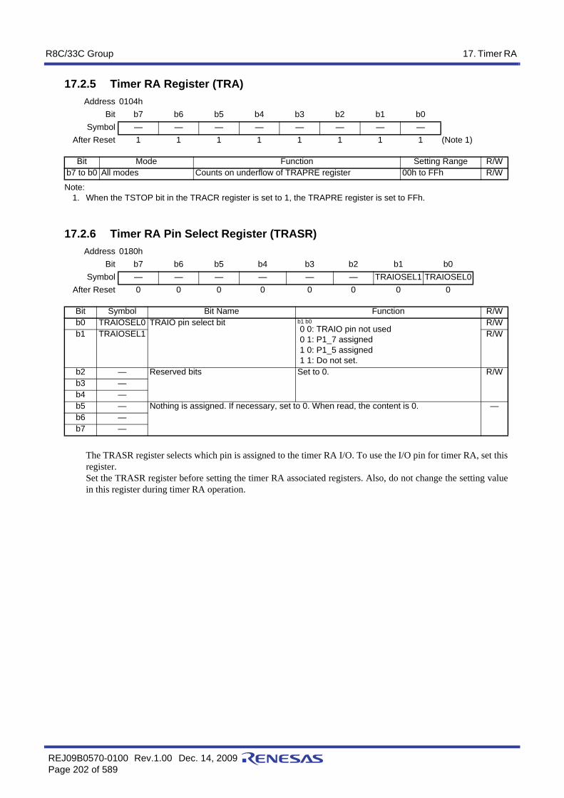
R8C/33C Group 17. Timer RA
REJ09B0570-0100 Rev.1.00 Dec. 14, 2009Page 202 of 589
17.2.5 Timer RA Register (TRA)
Note:1. When the TSTOP bit in the TRACR register is set to 1, the TRAPRE register is set to FFh.
17.2.6 Timer RA Pin Select Register (TRASR)
The TRASR register selects which pin is assigned to the timer RA I/O. To use the I/O pin for timer RA, set thisregister. Set the TRASR register before setting the timer RA associated registers. Also, do not change the setting valuein this register during timer RA operation.
Address 0104hBit b7 b6 b5 b4 b3 b2 b1 b0
Symbol — — — — — — — —After Reset 1 1 1 1 1 1 1 1 (Note 1)
Bit Mode Function Setting Range R/Wb7 to b0 All modes Counts on underflow of TRAPRE register 00h to FFh R/W
Address 0180hBit b7 b6 b5 b4 b3 b2 b1 b0
Symbol — — — — — — TRAIOSEL1 TRAIOSEL0After Reset 0 0 0 0 0 0 0 0
Bit Symbol Bit Name Function R/Wb0 TRAIOSEL0 TRAIO pin select bit b1 b0
0 0: TRAIO pin not used 0 1: P1_7 assigned 1 0: P1_5 assigned 1 1: Do not set.
R/Wb1 TRAIOSEL1 R/W
b2 — Reserved bits Set to 0. R/Wb3 —b4 —b5 — Nothing is assigned. If necessary, set to 0. When read, the content is 0. —b6 —b7 —

R8C/33C Group 17. Timer RA
REJ09B0570-0100 Rev.1.00 Dec. 14, 2009Page 203 of 589
17.3 Timer ModeIn this mode, the timer counts an internally generated count source (refer to Table 17.2 Timer ModeSpecifications).
17.3.1 Timer RA I/O Control Register (TRAIOC) in Timer Mode
Table 17.2 Timer Mode SpecificationsItem Specification
Count sources f1, f2, f8, fOCO, fC32, fCCount operations • Decrement
• When the timer underflows, the contents of the reload register are reloaded and the count is continued.
Divide ratio 1/(n+1)(m+1)n: Value set in TRAPRE register, m: Value set in TRA register
Count start condition 1 (count starts) is written to the TSTART bit in the TRACR register.Count stop conditions • 0 (count stops) is written to the TSTART bit in the TRACR register.
• 1 (count forcibly stops) is written to the TSTOP bit in the TRACR register.Interrupt request generation timing
When timer RA underflows [timer RA interrupt].
TRAIO pin function Programmable I/O portTRAO pin function Programmable I/O portRead from timer The count value can be read by reading registers TRA and TRAPRE.Write to timer • When registers TRAPRE and TRA are written while the count is stopped,
values are written to both the reload register and counter.• When registers TRAPRE and TRA are written during the count, values are
written to the reload register and counter (refer to 17.3.2 Timer Write Control during Count Operation).
Address 0101hBit b7 b6 b5 b4 b3 b2 b1 b0
Symbol TIOGT1 TIOGT0 TIPF1 TIPF0 — TOENA TOPCR TEDGSELAfter Reset 0 0 0 0 0 0 0 0
Bit Symbol Bit Name Function R/Wb0 TEDGSEL TRAIO polarity switch bit Set to 0 in timer mode. R/Wb1 TOPCR TRAIO output control bit R/Wb2 TOENA TRAO output enable bit R/Wb3 — Reserved bit Set to 0. R/Wb4 TIPF0 TRAIO input filter select bit Set to 0 in timer mode. R/Wb5 TIPF1 R/Wb6 TIOGT0 TRAIO event input control bit R/Wb7 TIOGT1 R/W

R8C/33C Group 17. Timer RA
REJ09B0570-0100 Rev.1.00 Dec. 14, 2009Page 204 of 589
17.3.2 Timer Write Control during Count OperationTimer RA has a prescaler and a timer (which counts the prescaler underflows). The prescaler and timer eachconsist of a reload register and a counter. When writing to the prescaler or timer, values are written to both thereload register and counter.However, values are transferred from the reload register to the counter of the prescaler in synchronization withthe count source. In addition, values are transferred from the reload register to the counter of the timer insynchronization with prescaler underflows. Therefore, if the prescaler or timer is written to when countoperation is in progress, the counter value is not updated immediately after the WRITE instruction is executed.Figure 17.2 shows an Operating Example of Timer RA when Counter Value is Rewritten during CountOperation.
Figure 17.2 Operating Example of Timer RA when Counter Value is Rewritten during Count Operation
Count source
Reload register oftimer RA prescaler
IR bit in TRAICregister 0
Counter oftimer RA prescaler
Reload register oftimer RA
Counter of timer RA
Set 01h to the TRAPRE register and 25h tothe TRA register by a program.
After writing, the reload register iswritten to at the first count source.
Reload atsecond countsource
Reload atunderflow
After writing, the reload register iswritten to at the first underflow.
Reload at the second underflow
The IR bit remains unchanged until underflow isgenerated by a new value.
05h 04h 01h 00h 01h 00h 01h 00h 01h 00h06h
New value (01h)Previous value
New value (25h)Previous value
03h 24h02h 25h
The above applies under the following conditions.Both bits TSTART and TCSTF in the TRACR register are set to 1 (during count).

R8C/33C Group 17. Timer RA
REJ09B0570-0100 Rev.1.00 Dec. 14, 2009Page 205 of 589
17.4 Pulse Output ModeIn pulse output mode, the internally generated count source is counted, and a pulse with inverted polarity isoutput from the TRAIO pin each time the timer underflows (refer to Table 17.3 Pulse Output ModeSpecifications).
Note:1. The level of the output pulse becomes the level when the pulse output starts when the TRAMR
register is written to.
Table 17.3 Pulse Output Mode SpecificationsItem Specification
Count sources f1, f2, f8, fOCO, fC32, fCCount operations • Decrement
• When the timer underflows, the contents in the reload register is reloaded and the count is continued.
Divide ratio 1/(n+1)(m+1)n: Value set in TRAPRE register, m: Value set in TRA register
Count start condition 1 (count starts) is written to the TSTART bit in the TRACR register.Count stop conditions • 0 (count stops) is written to the TSTART bit in the TRACR register.
• 1 (count forcibly stops) is written to the TSTOP bit in the TRACR register.Interrupt request generation timing
When timer RA underflows [timer RA interrupt].
TRAIO pin function Pulse output, programmable output portTRAO pin function Programmable I/O port or inverted output of TRAIORead from timer The count value can be read by reading registers TRA and TRAPRE.Write to timer • When registers TRAPRE and TRA are written while the count is stopped, values
are written to both the reload register and counter.• When registers TRAPRE and TRA are written during the count, values are
written to the reload register and counter (refer to 17.3.2 Timer Write Control during Count Operation).
Selectable functions • TRAIO signal polarity switch functionThe level when the pulse output starts is selected by the TEDGSEL bit in the TRAIOC register. (1)
• TRAO output functionPulses inverted from the TRAIO output polarity can be output from the TRAO pin (selectable by the TOENA bit in the TRAIOC register).
• Pulse output stop functionOutput from the TRAIO pin is stopped by the TOPCR bit in the TRAIOC register.
• TRAIO pin select functionP1_5 or P1_7 is selected by bits TRAIOSEL0 to TRAIOSEL1 in the TRASR register.

R8C/33C Group 17. Timer RA
REJ09B0570-0100 Rev.1.00 Dec. 14, 2009Page 206 of 589
17.4.1 Timer RA I/O Control Register (TRAIOC) in Pulse Output ModeAddress 0101h
Bit b7 b6 b5 b4 b3 b2 b1 b0Symbol TIOGT1 TIOGT0 TIPF1 TIPF0 — TOENA TOPCR TEDGSEL
After Reset 0 0 0 0 0 0 0 0
Bit Symbol Bit Name Function R/Wb0 TEDGSEL TRAIO polarity switch bit 0: TRAIO output starts at “H”
1: TRAIO output starts at “L”R/W
b1 TOPCR TRAIO output control bit 0: TRAIO output1: TRAIO output disabled
R/W
b2 TOENA TRAO output enable bit 0: TRAO output disabled1: TRAO output (inverted TRAIO output from the
port)
R/W
b3 — Reserved bit Set to 0. R/Wb4 TIPF0 TRAIO input filter select bit Set to 0 in pulse output mode. R/Wb5 TIPF1 R/Wb6 TIOGT0 TRAIO event input control bit R/Wb7 TIOGT1 R/W

R8C/33C Group 17. Timer RA
REJ09B0570-0100 Rev.1.00 Dec. 14, 2009Page 207 of 589
17.5 Event Counter ModeIn event counter mode, external signal inputs to the TRAIO pin are counted (refer to Table 17.4 EventCounter Mode Specifications).
Note:1. The level of the output pulse becomes the level when the pulse output starts when the TRAMR
register is written to.
Table 17.4 Event Counter Mode SpecificationsItem Specification
Count source External signal which is input to TRAIO pin (active edge selectable by a program)Count operations • Decrement
• When the timer underflows, the contents of the reload register are reloaded and the count is continued.
Divide ratio 1/(n+1)(m+1)n: setting value of TRAPRE register, m: setting value of TRA register
Count start condition 1 (count starts) is written to the TSTART bit in the TRACR register.Count stop conditions • 0 (count stops) is written to the TSTART bit in the TRACR register.
• 1 (count forcibly stops) is written to the TSTOP bit in the TRACR register.Interrupt request generation timing
When timer RA underflows [timer RA interrupt].
TRAIO pin function Count source inputTRAO pin function Programmable I/O port or pulse output (1)
Read from timer The count value can be read by reading registers TRA and TRAPRE.Write to timer • When registers TRAPRE and TRA are written while the count is stopped, values
are written to both the reload register and counter.• When registers TRAPRE and TRA are written during the count, values are
written to the reload register and counter (refer to 17.3.2 Timer Write Control during Count Operation).
Selectable functions • TRAIO input polarity switch functionThe active edge of the count source is selected by the TEDGSEL bit in the TRAIOC register.
• Count source input pin select functionP1_5 or P1_7 is selected by bits TRAIOSEL0 to TRAIOSEL1 in the TRASR register.
• Pulse output functionPulses of inverted polarity can be output from the TRAO pin each time the timer underflows (selectable by the TOENA bit in the TRAIOC register). (1)
• Digital filter functionWhether enabling or disabling the digital filter and the sampling frequency is selected by bits TIPF0 and TIPF1 in the TRAIOC register.
• Event input control functionThe enabled period for the event input to the TRAIO pin is selected by bits TIOGT0 and TIOGT1 in the TRAIOC register.

R8C/33C Group 17. Timer RA
REJ09B0570-0100 Rev.1.00 Dec. 14, 2009Page 208 of 589
17.5.1 Timer RA I/O Control Register (TRAIOC) in Event Counter Mode
Note:1. When the same value from the TRAIO pin is sampled three times continuously, the input is determined.
Address 0101hBit b7 b6 b5 b4 b3 b2 b1 b0
Symbol TIOGT1 TIOGT0 TIPF1 TIPF0 — TOENA TOPCR TEDGSELAfter Reset 0 0 0 0 0 0 0 0
Bit Symbol Bit Name Function R/Wb0 TEDGSEL TRAIO polarity switch bit 0: Starts counting at rising edge of the TRAIO input
and TRAO starts output at “L”1: Starts counting at falling edge of the TRAIO input
and TRAO starts output at “H”
R/W
b1 TOPCR TRAIO output control bit Set to 0 in event counter mode. R/Wb2 TOENA TRAO output enable bit 0: TRAO output disabled
1: TRAO outputR/W
b3 — Reserved bit Set to 0. R/Wb4 TIPF0 TRAIO input filter select bit (1) b5 b4
0 0: No filter 0 1: Filter with f1 sampling 1 0: Filter with f8 sampling 1 1: Filter with f32 sampling
R/Wb5 TIPF1 R/W
b6 TIOGT0 TRAIO event input control bit b7 b6 0 0: Event input always enabled 0 1: Do not set. 1 0: Event input enabled for "L" period of TRCIOD
(timer RC output) 1 1: Do not set.
R/Wb7 TIOGT1 R/W

R8C/33C Group 17. Timer RA
REJ09B0570-0100 Rev.1.00 Dec. 14, 2009Page 209 of 589
17.6 Pulse Width Measurement ModeIn pulse width measurement mode, the pulse width of an external signal input to the TRAIO pin is measured(refer to Table 17.5 Pulse Width Measurement Mode Specifications).Figure 17.3 shows an Operating Example of Pulse Width Measurement Mode.
Table 17.5 Pulse Width Measurement Mode SpecificationsItem Specification
Count sources f1, f2, f8, fOCO, fC32, fCCount operations • Decrement
• Continuously counts the selected signal only when measurement pulse is “H” level, or conversely only “L” level.
• When the timer underflows, the contents of the reload register are reloaded and the count is continued.
Count start condition 1 (count starts) is written to the TSTART bit in the TRACR register.Count stop conditions • 0 (count stops) is written to the TSTART bit in the TRACR register.
• 1 (count forcibly stops) is written to the TSTOP bit in the TRACR register.Interrupt request generation timing
• When timer RA underflows [timer RA interrupt].• Rising or falling of the TRAIO input (end of measurement period) [timer RA
interrupt]TRAIO pin function Measured pulse inputTRAO pin function Programmable I/O portRead from timer The count value can be read by reading registers TRA and TRAPRE.Write to timer • When registers TRAPRE and TRA are written while the count is stopped,
values are written to both the reload register and counter.• When registers TRAPRE and TRA are written during the count, values are
written to the reload register and counter (refer to 17.3.2 Timer Write Control during Count Operation).
Selectable functions • Measurement level settingThe “H” level or “L” level period is selected by the TEDGSEL bit in the TRAIOC register.
• Measured pulse input pin select functionP1_5 or P1_7 is selected by bits TRAIOSEL0 to TRAIOSEL1 in the TRASR register.
• Digital filter functionWhether enabling or disabling the digital filter and the sampling frequency is selected by bits TIPF0 and TIPF1 in the TRAIOC register.

R8C/33C Group 17. Timer RA
REJ09B0570-0100 Rev.1.00 Dec. 14, 2009Page 210 of 589
17.6.1 Timer RA I/O Control Register (TRAIOC) in Pulse Width MeasurementMode
Note:1. When the same value from the TRAIO pin is sampled three times continuously, the input is determined.
Address 0101hBit b7 b6 b5 b4 b3 b2 b1 b0
Symbol TIOGT1 TIOGT0 TIPF1 TIPF0 — TOENA TOPCR TEDGSELAfter Reset 0 0 0 0 0 0 0 0
Bit Symbol Bit Name Function R/Wb0 TEDGSEL TRAIO polarity switch bit 0: TRAIO input starts at “L”
1: TRAIO input starts at “H”R/W
b1 TOPCR TRAIO output control bit Set to 0 in pulse width measurement mode. R/Wb2 TOENA TRAO output enable bit R/Wb3 — Reserved bit Set to 0. R/Wb4 TIPF0 TRAIO input filter select bit (1) b5 b4
0 0: No filter 0 1: Filter with f1 sampling 1 0: Filter with f8 sampling 1 1: Filter with f32 sampling
R/Wb5 TIPF1 R/W
b6 TIOGT0 TRAIO event input control bit Set to 0 in pulse width measurement mode. R/Wb7 TIOGT1 R/W

R8C/33C Group 17. Timer RA
REJ09B0570-0100 Rev.1.00 Dec. 14, 2009Page 211 of 589
17.6.2 Operating Example
Figure 17.3 Operating Example of Pulse Width Measurement Mode
FFFFh
n
0000h
Con
tent
of c
ount
er (h
ex)
n = high level: the contents of TRA register, low level: the contents of TRAPRE register
Count start
Count stop
Underflow
Period
TSTART bit inTRACR register
Measured pulse(TRAIO pin input)
TEDGF bit inTRACR register
TUNDF bit inTRACR register
• “H” level width of measured pulse is measured. (TEDGSEL = 1)• TRAPRE = FFh
Set to 1 by program
IR bit in TRAICregister
Set to 0 by program
Count stop
Count start
Set to 0 when interrupt request is acknowledged, or set by program
Count start
Set to 0 by program
The above applies under the following conditions.

R8C/33C Group 17. Timer RA
REJ09B0570-0100 Rev.1.00 Dec. 14, 2009Page 212 of 589
17.7 Pulse Period Measurement ModeIn pulse period measurement mode, the pulse period of an external signal input to the TRAIO pin is measured(refer to Table 17.6 Pulse Period Measurement Mode Specifications).Figure 17.4 shows an Operating Example of Pulse Period Measurement Mode.
Note:1. Input a pulse with a period longer than twice the timer RA prescaler period. Input a pulse with a
longer “H” and “L” width than the timer RA prescaler period. If a pulse with a shorter period is input to the TRAIO pin, the input may be ignored.
Table 17.6 Pulse Period Measurement Mode SpecificationsItem Specification
Count sources f1, f2, f8, fOCO, fC32, fCCount operations • Decrement
• After the active edge of the measured pulse is input, the contents of the read-out buffer are retained at the first underflow of timer RA prescaler. Then timer RA reloads the contents in the reload register at the second underflow of timer RA prescaler and continues counting.
Count start condition 1 (count starts) is written to the TSTART bit in the TRACR register.Count stop conditions • 0 (count stops) is written to TSTART bit in the TRACR register.
• 1 (count forcibly stops) is written to the TSTOP bit in the TRACR register.Interrupt request generation timing
• When timer RA underflows or reloads [timer RA interrupt].• Rising or falling of the TRAIO input (end of measurement period) [timer RA
interrupt]TRAIO pin function Measured pulse input (1)
TRAO pin function Programmable I/O portRead from timer The count value can be read by reading registers TRA and TRAPRE.Write to timer • When registers TRAPRE and TRA are written while the count is stopped,
values are written to both the reload register and counter.• When registers TRAPRE and TRA are written during the count, values are
written to the reload register and counter (refer to 17.3.2 Timer Write Control during Count Operation).
Selectable functions • Measurement period selectionThe measurement period of the input pulse is selected by the TEDGSEL in the TRAIOC register.
• Measured pulse input pin select functionP1_5 or P1_7 is selected by bits TRAIOSEL0 to TRAIOSEL1 in the TRASR register.
• Digital filter functionWhether enabling or disabling the digital filter and the sampling frequency is selected by bits TIPF0 and TIPF1 in the TRAIOC register.

R8C/33C Group 17. Timer RA
REJ09B0570-0100 Rev.1.00 Dec. 14, 2009Page 213 of 589
17.7.1 Timer RA I/O Control Register (TRAIOC) in Pulse Period MeasurementMode
Note:1. When the same value from the TRAIO pin is sampled three times continuously, the input is determined.
Address 0101hBit b7 b6 b5 b4 b3 b2 b1 b0
Symbol TIOGT1 TIOGT0 TIPF1 TIPF0 — TOENA TOPCR TEDGSELAfter Reset 0 0 0 0 0 0 0 0
Bit Symbol Bit Name Function R/Wb0 TEDGSEL TRAIO polarity switch bit 0: Measures measurement pulse from one rising
edge to next rising edge1: Measures measurement pulse from one falling
edge to next falling edge
R/W
b1 TOPCR TRAIO output control bit Set to 0 in pulse period measurement mode. R/Wb2 TOENA TRAO output enable bit R/Wb3 — Reserved bit Set to 0. R/Wb4 TIPF0 TRAIO input filter select bit (1) b5 b4
0 0: No filter 0 1: Filter with f1 sampling 1 0: Filter with f8 sampling 1 1: Filter with f32 sampling
R/Wb5 TIPF1 R/W
b6 TIOGT0 TRAIO event input control bit Set to 0 in pulse period measurement mode. R/Wb7 TIOGT1 R/W

R8C/33C Group 17. Timer RA
REJ09B0570-0100 Rev.1.00 Dec. 14, 2009Page 214 of 589
17.7.2 Operating Example
Figure 17.4 Operating Example of Pulse Period Measurement Mode
Underflow signal oftimer RA prescaler
Notes:1. The contents of the read-out buffer can be read by reading the TRA register in pulse period measurement mode.2. After an active edge of the measured pulse is input, the TEDGF bit in the TRACR register is set to 1 (active edge received) when the
timer RA prescaler underflows for the second time.3. The TRA register should be read before the next active edge is input after the TEDGF bit is set to 1 (active edge received).
The contents in the read-out buffer are retained until the TRA register is read. If the TRA register is not read before the next active edgeis input, the measured result of the previous period is retained.
4. To set to 0 by a program, use a MOV instruction to write 0 to the TEDGF bit in the TRACR register. At the same time, write 1 to theTUNDF bit in the TRACR register.
5. To set to 0 by a program, use a MOV instruction to write 0 to the TUNDF bit. At the same time, write 1 to the TEDGF bit.6. Bits TUNDF and TEDGF are both set to 1 if timer RA underflows and reloads on an active edge simultaneously.
0Eh 0Dh 0Fh 0Eh 0Dh 0Ch 0Bh 0Ah 09h 0Fh 0Eh 0Dh 01h 00h 0Fh 0Eh0Fh
0Dh0Fh 0Bh 0Ah 0Dh 01h 00h 0Fh 0Eh09h
TSTART bit inTRACR register
TEDGF bit inTRACR register
Measurement pulse(TRAIO pin input)
Contents of TRA
Contents of read-outbuffer (1)
IR bit in TRAICregister
TUNDF bit inTRACR register
Set to 1 by program
Count start
TRA reloaded
TRA read (3)
Retained
Set to 0 by program
Conditions: The period from one rising edge to the next rising edge of the measured pulse is measured (TEDGSEL = 0) withthe default value of the TRA register as 0Fh.
0Eh
TRA reloaded
Retained
Set to 0 when interrupt request is acknowledged, or set by program
Set to 0 by program
Underflow
(Note 2) (Note 2)
(Note 4)(Note 6)
(Note 5)

R8C/33C Group 17. Timer RA
REJ09B0570-0100 Rev.1.00 Dec. 14, 2009Page 215 of 589
17.8 Notes on Timer RA• Timer RA stops counting after a reset. Set the values in the timer RA and timer RA prescalers before the count
starts.• Even if the prescaler and timer RA are read out in 16-bit units, these registers are read 1 byte at a time by the
MCU. Consequently, the timer value may be updated during the period when these two registers are being read.• In pulse width measurement mode and pulse period measurement mode, bits TEDGF and TUNDF in the TRACR
register can be set to 0 by writing 0 to these bits by a program. However, these bits remain unchanged if 1 iswritten. When using the READ-MODIFY-WRITE instruction for the TRACR register, the TEDGF or TUNDFbit may be set to 0 although these bits are set to 1 while the instruction is being executed. In this case, write 1 tothe TEDGF or TUNDF bit which is not supposed to be set to 0 with the MOV instruction.
• When changing to pulse period measurement mode from another mode, the contents of bits TEDGF and TUNDFare undefined. Write 0 to bits TEDGF and TUNDF before the count starts.
• The TEDGF bit may be set to 1 by the first timer RA prescaler underflow generated after the count starts.• When using the pulse period measurement mode, leave two or more periods of the timer RA prescaler
immediately after the count starts, then set the TEDGF bit to 0.• The TCSTF bit retains 0 (count stops) for 0 to 1 cycle of the count source after setting the TSTART bit to 1 (count
starts) while the count is stopped.During this time, do not access registers associated with timer RA (1) other than the TCSTF bit. Timer RA startscounting at the first valid edge of the count source after the TCSTF bit is set to 1 (during count).The TCSTF bit remains 1 for 0 to 1 cycle of the count source after setting the TSTART bit to 0 (count stops)while the count is in progress. Timer RA counting is stopped when the TCSTF bit is set to 0.During this time, do not access registers associated with timer RA (1) other than the TCSTF bit.
Note:1. Registers associated with timer RA: TRACR, TRAIOC, TRAMR, TRAPRE, and TRA.
• When the TRAPRE register is continuously written during count operation (TCSTF bit is set to 1), allow three ormore cycles of the count source clock for each write interval.
• When the TRA register is continuously written during count operation (TCSTF bit is set to 1), allow three ormore cycles of the prescaler underflow for each write interval.

R8C/33C Group 18. Timer RB
REJ09B0570-0100 Rev.1.00 Dec. 14, 2009Page 216 of 589
18. Timer RBTimer RB is an 8-bit timer with an 8-bit prescaler.
18.1 OverviewThe prescaler and timer each consist of a reload register and counter (refer to Tables 18.2 to 18.5 theSpecifications of Each Mode). Timer RB has timer RB primary and timer RB secondary as reload registers.The count source for timer RB is the operating clock that regulates the timing of timer operations such as countingand reloading.Figure 18.1 shows a Timer RB Block Diagram. Table 18.1 lists Pin Configuration of Timer RB.
Timer RB has four operation modes listed as follows:• Timer mode: The timer counts an internal count source (peripheral
function clock or timer RA underflows).• Programmable waveform generation mode: The timer outputs pulses of a given width successively.• Programmable one-shot generation mode: The timer outputs a one-shot pulse.• Programmable wait one-shot generation mode: The timer outputs a delayed one-shot pulse.
Figure 18.1 Timer RB Block Diagram
Table 18.1 Pin Configuration of Timer RB
Pin Name Assigned Pin I/O Function
TRBO P1_3 or P3_1 Output
Pulse output (Programmable waveform generation mode, Programmable one-shot generation mode, Programmable wait one-shot generation mode)
INT0PL bit
= 00b= 01b
= 11b
f8f1
= 10bTimer RA underflow
Bits TCK1 to TCK0
TSTART bit
TRBPRE register(prescaler)
Timer RB interrupt
INT0 interrupt
Write 1 to TSTOP bit
Toggleflip-flop
Q
Q CLR
CK
TOPL = 1
TOPL = 0P1_3 bit in P1 register orP3_1 bit in P3 register
f2 TMOD1 to TMOD0 bits= 10b or 11b
TOSSTF bit
Polarityselect
INOSEG bit
Input polarityselected to be oneedge or both edges
Digital filterINT0 pin
INT0EN bit
Bits TMOD1 to TMOD0= 01b, 10b, 11b
Counter
Reloadregister
Counter (timer RB)
Reloadregister
TRBPRregister
Data busTRBSCregister
Reloadregister
TCKCUT bit
INOSTG bit
TSTART, TCSTF: Bits in TRBCR registerTOSSTF: Bit in TRBOCR registerTOPL, TOCNT, INOSTG, INOSEG: Bits in TRBIOC registerTMOD1 to TMOD0, TCK1 to TCK0, TCKCUT: Bits in TRBMR register
(Timer)
TOCNT = 0
TOCNT = 1
Bits TMOD1 to TMOD0= 01b, 10b, 11b
TRBO pin (1)
Note:1. Bit TRBOSEL0 in the TRBRCSR register is used to select which pin is assigned.

R8C/33C Group 18. Timer RB
REJ09B0570-0100 Rev.1.00 Dec. 14, 2009Page 217 of 589
18.2 Registers
18.2.1 Timer RB Control Register (TRBCR)
Notes:1. Refer to 18.7 Notes on Timer RB for precautions regarding bits TSTART, TCSTF and TSTOP.2. When the TSTOP bit is set to 1, registers TRBPRE, TRBSC, TRBPR, and bits TSTART and TCSTF, and the
TOSSTF bit in the TRBOCR register are set to values after a reset.3. Indicates that count operation is in progress in timer mode or programmable waveform mode. In programmable
one-shot generation mode or programmable wait one-shot generation mode, indicates that a one-shot pulsetrigger has been acknowledged.
18.2.2 Timer RB One-Shot Control Register (TRBOCR)
Note:1. When 1 is set to the TSTOP bit in the TRBCR register, the TOSSTF bit is set to 0.
This register is enabled when bits TMOD1 to TMOD0 in the TRBMR register is set to 10b (programmable one-shot generation mode) or 11b (programmable wait one-shot generation mode).
Address 0108hBit b7 b6 b5 b4 b3 b2 b1 b0
Symbol — — — — — TSTOP TCSTF TSTARTAfter Reset 0 0 0 0 0 0 0 0
Bit Symbol Bit Name Function R/Wb0 TSTART Timer RB count start bit (1) 0: Count stops
1: Count startsR/W
b1 TCSTF Timer RB count status flag (1) 0: Count stops1: During count (3)
R
b2 TSTOP Timer RB count forcible stop bit (1, 2) When this bit is set to 1, the count is forcibly stopped. When read, the content is 0.
R/W
b3 — Nothing is assigned. If necessary, set to 0. When read, the content is 0. —b4 —b5 —b6 —b7 —
Address 0109hBit b7 b6 b5 b4 b3 b2 b1 b0
Symbol — — — — — TOSSTF TOSSP TOSSTAfter Reset 0 0 0 0 0 0 0 0
Bit Symbol Bit Name Function R/Wb0 TOSST Timer RB one-shot start bit When this bit is set to 1, one-shot trigger
generated. When read, its content is 0.R/W
b1 TOSSP Timer RB one-shot stop bit When this bit is set to 1, counting of one-shot pulses (including programmable wait one-shot pulses) stops. When read, the content is 0.
R/W
b2 TOSSTF Timer RB one-shot status flag (1) 0: One-shot stopped1: One-shot operating (Including wait period)
R
b3 — Nothing is assigned. If necessary, set to 0. When read, the content is 0. —b4 —b5 —b6 —b7 —
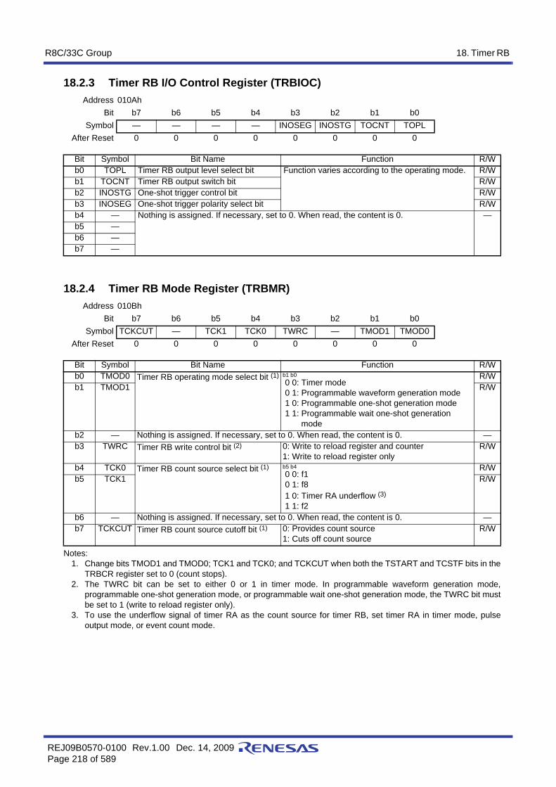
R8C/33C Group 18. Timer RB
REJ09B0570-0100 Rev.1.00 Dec. 14, 2009Page 218 of 589
18.2.3 Timer RB I/O Control Register (TRBIOC)
18.2.4 Timer RB Mode Register (TRBMR)
Notes:1. Change bits TMOD1 and TMOD0; TCK1 and TCK0; and TCKCUT when both the TSTART and TCSTF bits in the
TRBCR register set to 0 (count stops).2. The TWRC bit can be set to either 0 or 1 in timer mode. In programmable waveform generation mode,
programmable one-shot generation mode, or programmable wait one-shot generation mode, the TWRC bit mustbe set to 1 (write to reload register only).
3. To use the underflow signal of timer RA as the count source for timer RB, set timer RA in timer mode, pulseoutput mode, or event count mode.
Address 010AhBit b7 b6 b5 b4 b3 b2 b1 b0
Symbol — — — — INOSEG INOSTG TOCNT TOPLAfter Reset 0 0 0 0 0 0 0 0
Bit Symbol Bit Name Function R/Wb0 TOPL Timer RB output level select bit Function varies according to the operating mode. R/Wb1 TOCNT Timer RB output switch bit R/Wb2 INOSTG One-shot trigger control bit R/Wb3 INOSEG One-shot trigger polarity select bit R/Wb4 — Nothing is assigned. If necessary, set to 0. When read, the content is 0. —b5 —b6 —b7 —
Address 010BhBit b7 b6 b5 b4 b3 b2 b1 b0
Symbol TCKCUT — TCK1 TCK0 TWRC — TMOD1 TMOD0After Reset 0 0 0 0 0 0 0 0
Bit Symbol Bit Name Function R/Wb0 TMOD0 Timer RB operating mode select bit (1) b1 b0
0 0: Timer mode 0 1: Programmable waveform generation mode 1 0: Programmable one-shot generation mode 1 1: Programmable wait one-shot generation
mode
R/Wb1 TMOD1 R/W
b2 — Nothing is assigned. If necessary, set to 0. When read, the content is 0. —b3 TWRC Timer RB write control bit (2) 0: Write to reload register and counter
1: Write to reload register onlyR/W
b4 TCK0 Timer RB count source select bit (1) b5 b4 0 0: f1 0 1: f8 1 0: Timer RA underflow (3)
1 1: f2
R/Wb5 TCK1 R/W
b6 — Nothing is assigned. If necessary, set to 0. When read, the content is 0. —b7 TCKCUT Timer RB count source cutoff bit (1) 0: Provides count source
1: Cuts off count sourceR/W

R8C/33C Group 18. Timer RB
REJ09B0570-0100 Rev.1.00 Dec. 14, 2009Page 219 of 589
18.2.5 Timer RB Prescaler Register (TRBPRE)
When the TSTOP bit in the TRBCR register is set to 1, the TRBPRE register is set to FFh.
18.2.6 Timer RB Secondary Register (TRBSC)
Notes:1. The values of registers TRBPR and TRBSC are reloaded to the counter alternately and counted.2. The count value can be read out by reading the TRBPR register even when the secondary period is being
counted.
When the TSTOP bit in the TRBCR register is set to 1, the TRBSC register is set to FFh.To write to the TRBSC register, perform the following steps.(1) Write the value to the TRBSC register.(2) Write the value to the TRBPR register. (If the value does not change, write the same value second time.)
Address 010ChBit b7 b6 b5 b4 b3 b2 b1 b0
Symbol — — — — — — — —After Reset 1 1 1 1 1 1 1 1
Bit Mode Function Setting Range R/Wb7 to b0 Timer mode Counts an internal count source or
timer RA underflows00h to FFh R/W
Programmable waveform generation mode
00h to FFh R/W
Programmable one-shot generation mode
00h to FFh R/W
Programmable wait one-shot generation mode
00h to FFh R/W
Address 010DhBit b7 b6 b5 b4 b3 b2 b1 b0
Symbol — — — — — — — —After Reset 1 1 1 1 1 1 1 1
Bit Mode Function Setting Range R/Wb7 to b0 Timer mode Disabled 00h to FFh —
Programmable waveform generation mode
Counts timer RB prescaler underflows (1) 00h to FFh W (2)
Programmable one-shot generation mode
Disabled 00h to FFh —
Programmable wait one-shot generation mode
Counts timer RB prescaler underflows (one-shot width is counted)
00h to FFh W (2)

R8C/33C Group 18. Timer RB
REJ09B0570-0100 Rev.1.00 Dec. 14, 2009Page 220 of 589
18.2.7 Timer RB Primary Register (TRBPR)
Note:1. The values of registers TRBPR and TRBSC are reloaded to the counter alternately and counted.
When the TSTOP bit in the TRBCR register is set to 1, the TRBPR register is set to FFh.
18.2.8 Timer RB/RC Pin Select Register (TRBRCSR)
The TRBRCSR register selects which pin is assigned to the timer RB and timer RC I/O. To use the I/O pin fortimer RB and timer RC, set this register. Set the TRBOSEL0 bit before setting the timer RB associated registers. Set bits TRCCLKSEL0 andTRCCLKSEL1 before setting the timer RC associated registers. Also, do not change the setting values of theTRBOSEL0 bit during timer RB operation. Do not change the setting values of bits TRCCLKSEL0 andTRCCLKSEL1 during timer RC operation.
Address 010EhBit b7 b6 b5 b4 b3 b2 b1 b0
Symbol — — — — — — — —After Reset 1 1 1 1 1 1 1 1
Bit Mode Function Setting Range R/Wb7 to b0 Timer mode Counts timer RB prescaler underflows 00h to FFh R/W
Programmable waveform generation mode
Counts timer RB prescaler underflows (1) 00h to FFh R/W
Programmable one-shot generation mode
Counts timer RB prescaler underflows(one-shot width is counted)
00h to FFh R/W
Programmable wait one-shot generation mode
Counts timer RB prescaler underflows(wait period width is counted)
00h to FFh R/W
Address 0181hBit b7 b6 b5 b4 b3 b2 b1 b0
Symbol — — TRCCLKSEL1 TRCCLKSEL0 — — — TRBOSEL0After Reset 0 0 0 0 0 0 0 0
Bit Symbol Bit Name Function R/Wb0 TRBOSEL0 TRBO pin select bit 0: P1_3 assigned
1: P3_1 assignedR/W
b1 — Reserved bit Set to 0. R/Wb2 — Nothing is assigned. If necessary, set to 0. When read, the content is 0. —b3 —b4 TRCCLKSEL0 TRCCLK pin select bit b5 b4
0 0: TRCCLK pin not used 0 1: P1_4 assigned 1 0: P3_3 assigned 1 1: Do not set.
R/Wb5 TRCCLKSEL1 R/W
b6 — Reserved bit Set to 0. R/Wb7 — Nothing is assigned. If necessary, set to 0. When read, the content is 0. —

R8C/33C Group 18. Timer RB
REJ09B0570-0100 Rev.1.00 Dec. 14, 2009Page 221 of 589
18.3 Timer ModeIn timer mode, a count source which is internally generated or timer RA underflows are counted (refer to Table18.2 Timer Mode Specifications). Registers TRBOCR and TRBSC are not used in timer mode.
18.3.1 Timer RB I/O Control Register (TRBIOC) in Timer Mode
Table 18.2 Timer Mode SpecificationsItem Specification
Count sources f1, f2, f8, timer RA underflowCount operations • Decrement
• When the timer underflows, it reloads the reload register contents before the count continues (when timer RB underflows, the contents of timer RB primary reload register is reloaded).
Divide ratio 1/(n+1)(m+1)n: setting value in TRBPRE register, m: setting value in TRBPR register
Count start condition 1 (count starts) is written to the TSTART bit in the TRBCR register.Count stop conditions • 0 (count stops) is written to the TSTART bit in the TRBCR register.
• 1 (count forcibly stop) is written to the TSTOP bit in the TRBCR register.Interrupt request generation timing
When timer RB underflows [timer RB interrupt].
TRBO pin function Programmable I/O portINT0 pin function Programmable I/O port or INT0 interrupt inputRead from timer The count value can be read out by reading registers TRBPR and TRBPRE.Write to timer • When registers TRBPRE and TRBPR are written while the count is stopped,
values are written to both the reload register and counter. • When registers TRBPRE and TRBPR are written to while count operation is in
progress:If the TWRC bit in the TRBMR register is set to 0, the value is written to both the reload register and the counter.If the TWRC bit is set to 1, the value is written to the reload register only.(Refer to 18.3.2 Timer Write Control during Count Operation.)
Address 010AhBit b7 b6 b5 b4 b3 b2 b1 b0
Symbol — — — — INOSEG INOSTG TOCNT TOPLAfter Reset 0 0 0 0 0 0 0 0
Bit Symbol Bit Name Function R/Wb0 TOPL Timer RB output level select bit Set to 0 in timer mode. R/Wb1 TOCNT Timer RB output switch bit R/Wb2 INOSTG One-shot trigger control bit R/Wb3 INOSEG One-shot trigger polarity select bit R/Wb4 — Nothing is assigned. If necessary, set to 0. When read, the content is 0. —b5 —b6 —b7 —

R8C/33C Group 18. Timer RB
REJ09B0570-0100 Rev.1.00 Dec. 14, 2009Page 222 of 589
18.3.2 Timer Write Control during Count OperationTimer RB has a prescaler and a timer (which counts the prescaler underflows). The prescaler and timer eachconsist of a reload register and a counter. In timer mode, the TWRC bit in the TRBMR register can be used toselect whether writing to the prescaler or timer during count operation is performed to both the reload registerand counter or only to the reload register.However, values are transferred from the reload register to the counter of the prescaler in synchronization withthe count source. In addition, values are transferred from the reload register to the counter of the timer insynchronization with prescaler underflows. Therefore, even if the TWRC bit is set for writing to both the reloadregister and counter, the counter value is not updated immediately after the WRITE instruction is executed. Inaddition, if the TWRC bit is set for writing to the reload register only, the synchronization of the writing will beshifted if the prescaler value changes. Figure 18.2 shows an Operating Example of Timer RB when CounterValue is Rewritten during Count Operation.

R8C/33C Group 18. Timer RB
REJ09B0570-0100 Rev.1.00 Dec. 14, 2009Page 223 of 589
Figure 18.2 Operating Example of Timer RB when Counter Value is Rewritten during Count Operation
Count source
Reloads register oftimer RB prescaler
IR bit in TRBICregister 0
Counter oftimer RB prescaler
Reloads register oftimer RB
Counter of timer RB
Set 01h to the TRBPRE register and 25h tothe TRBPR register by a program.
After writing, the reload register iswritten with the first count source.
Reload withthe secondcount source
Reload onunderflow
After writing, the reload register iswritten on the first underflow.
Reload on the secondunderflow
The IR bit remains unchanged until underflowis generated by a new value.
When the TWRC bit is set to 0 (write to reload register and counter)
Count source
Reloads register oftimer RB prescaler
IR bit in TRBICregister
Counter oftimer RB prescaler
Reloads register oftimer RB
Counter of timer RB
Set 01h to the TRBPRE register and 25h tothe TRBPR register by a program.
After writing, the reload register iswritten with the first count source.
Reload onunderflow
After writing, the reload register iswritten on the first underflow.
Reload onunderflow
Only the prescaler values are updated,extending the duration until timer RB underflow.
When the TWRC bit is set to 1 (write to reload register only)
05h 04h 03h 02h 01h 00h 01h 00h 01h 00h06h 01h 00h 01h
03h 00h02h 01h 25h
New value (25h)Previous value
New value (01h)Previous value
New value (01h)Previous value
05h 04h 01h 00h 01h 00h 01h 00h 01h 00h06h
New value (25h)Previous value
03h 24h02h 25h
The above applies under the following conditions.Both bits TSTART and TCSTF in the TRBCR register are set to 1 (During count).

R8C/33C Group 18. Timer RB
REJ09B0570-0100 Rev.1.00 Dec. 14, 2009Page 224 of 589
18.4 Programmable Waveform Generation ModeIn programmable waveform generation mode, the signal output from the TRBO pin is inverted each time thecounter underflows, while the values in registers TRBPR and TRBSC are counted alternately (refer to Table 18.3Programmable Waveform Generation Mode Specifications). Counting starts by counting the setting value in theTRBPR register. The TRBOCR register is unused in this mode.Figure 18.3 shows an Operating Example of Timer RB in Programmable Waveform Generation Mode.
Notes:1. Even when counting the secondary period, the TRBPR register may be read.2. The set values are reflected in the waveform output beginning with the following primary period after writing to
the TRBPR register.3. The value written to the TOCNT bit is enabled by the following.
• When counting starts.• When a timer RB interrupt request is generated.
The contents after the TOCNT bit is changed are reflected from the output of the following primary period.
Table 18.3 Programmable Waveform Generation Mode SpecificationsItem Specification
Count sources f1, f2, f8, timer RA underflowCount operations • Decrement
• When the timer underflows, it reloads the contents of the primary reload and secondary reload registers alternately before the count continues.
Width and period of output waveform
Primary period: (n+1)(m+1)/fiSecondary period: (n+1)(p+1)/fiPeriod: (n+1)(m+1)+(p+1)/fifi: Count source frequencyn: Value set in TRBPRE register, m: Value set in TRBPR registerp: Value set in TRBSC register
Count start condition 1 (count start) is written to the TSTART bit in the TRBCR register.Count stop conditions • 0 (count stop) is written to the TSTART bit in the TRBCR register.
• 1 (count forcibly stop) is written to the TSTOP bit in the TRBCR register.Interrupt request generation timing
In half a cycle of the count source, after timer RB underflows during the secondary period (at the same time as the TRBO output change) [timer RB interrupt]
TRBO pin function Programmable output port or pulse output
INT0 pin function Programmable I/O port or INT0 interrupt inputRead from timer The count value can be read out by reading registers TRBPR and TRBPRE (1).Write to timer • When registers TRBPRE, TRBSC, and TRBPR are written while the count is stopped,
values are written to both the reload register and counter. • When registers TRBPRE, TRBSC, and TRBPR are written to during count operation,
values are written to the reload registers only. (2)
Selectable functions • Output level select functionThe output level during primary and secondary periods is selected by the TOPL bit in the TRBIOC register.
• TRBO pin output switch functionTimer RB pulse output or P3_1 (P1_3) latch output is selected by the TOCNT bit in the TRBIOC register. (3)

R8C/33C Group 18. Timer RB
REJ09B0570-0100 Rev.1.00 Dec. 14, 2009Page 225 of 589
18.4.1 Timer RB I/O Control Register (TRBIOC) in Programmable Waveform Generation Mode
Address 010AhBit b7 b6 b5 b4 b3 b2 b1 b0
Symbol — — — — INOSEG INOSTG TOCNT TOPLAfter Reset 0 0 0 0 0 0 0 0
Bit Symbol Bit Name Function R/Wb0 TOPL Timer RB output level select bit 0: Outputs “H” for primary period
Outputs “L” for secondary periodOutputs “L” when the timer is stopped
1: Outputs “L” for primary periodOutputs “H” for secondary periodOutputs “H” when the timer is stopped
R/W
b1 TOCNT Timer RB output switch bit 0: Outputs timer RB waveform1: Outputs value in P3_1 (P1_3) port register
R/W
b2 INOSTG One-shot trigger control bit Set to 0 in programmable waveform generation mode.
R/Wb3 INOSEG One-shot trigger polarity select bit R/Wb4 — Nothing is assigned. If necessary, set to 0. When read, the content is 0. —b5 —b6 —b7 —

R8C/33C Group 18. Timer RB
REJ09B0570-0100 Rev.1.00 Dec. 14, 2009Page 226 of 589
18.4.2 Operating Example
Figure 18.3 Operating Example of Timer RB in Programmable Waveform Generation Mode
IR bit in TRBICregister
Count source
Timer RB prescalerunderflow signal
Counter of timer RB
TRBO pin output
TOPL bit in TRBIOregister
Set to 1 by program
Set to 0 when interruptrequest is acknowledged,or set by program.
The above applies under the following conditions.
TSTART bit in TRBCRregister
01h 00h 02h
Timer RB secondary reloads Timer RB primary reloads
Set to 0 by program
TRBPRE = 01h, TRBPR = 01h, TRBSC = 02hTRBIOC register TOCNT = 0 (timer RB waveform is output from the TRBO pin)
02h 01h 00h 01h 00h
Primary period Primary periodSecondary period
Waveformoutput starts Waveform output inverted Waveform output starts
Initial output is the same levelas during secondary period.
R8C/33C Group 18. Timer RB
REJ09B0570-0100 Rev.1.00 Dec. 14, 2009Page 227 of 589
18.5 Programmable One-shot Generation ModeIn programmable one-shot generation mode, a one-shot pulse is output from the TRBO pin by a program or anexternal trigger input (input to the INT0 pin) (refer to Table 18.4 Programmable One-Shot Generation ModeSpecifications). When a trigger is generated, the timer starts operating from the point only once for a given periodequal to the set value in the TRBPR register. The TRBSC register is not used in this mode.Figure 18.4 shows an Operating Example of Programmable One-Shot Generation Mode.
Note:1. The set value is reflected at the following one-shot pulse after writing to the TRBPR register.
Table 18.4 Programmable One-Shot Generation Mode SpecificationsItem Specification
Count sources f1, f2, f8, timer RA underflowCount operations • Decrement the setting value in the TRBPR register
• When the timer underflows, it reloads the contents of the reload register before the count completes and the TOSSTF bit is set to 0 (one-shot stops).
• When the count stops, the timer reloads the contents of the reload register before it stops.
One-shot pulse output time
(n+1)(m+1)/fifi: Count source frequency,n: Setting value in TRBPRE register, m: Setting value in TRBPR register
Count start conditions • The TSTART bit in the TRBCR register is set to 1 (count starts) and the next trigger is generated
• Set the TOSST bit in the TRBOCR register to 1 (one-shot starts)• Input trigger to the INT0 pin
Count stop conditions • When reloading completes after timer RB underflows during primary period• When the TOSSP bit in the TRBOCR register is set to 1 (one-shot stops)• When the TSTART bit in the TRBCR register is set to 0 (stops counting)• When the TSTOP bit in the TRBCR register is set to 1 (forcibly stops counting)
Interrupt request generation timing
In half a cycle of the count source, after the timer underflows (at the same time as the TRBO output ends) [timer RB interrupt]
TRBO pin function Pulse outputINT0 pin functions • When the INOSTG bit in the TRBIOC register is set to 0 (INT0 one-shot trigger
disabled): programmable I/O port or INT0 interrupt input• When the INOSTG bit in the TRBIOC register is set to 1 (INT0 one-shot trigger
enabled): external trigger (INT0 interrupt input)Read from timer The count value can be read out by reading registers TRBPR and TRBPRE.Write to timer • When registers TRBPRE and TRBPR are written while the count is stopped,
values are written to both the reload register and counter. • When registers TRBPRE and TRBPR are written during the count, values are
written to the reload register only (the data is transferred to the counter at the following reload) (1).
Selectable functions • Output level select functionThe output level of the one-shot pulse waveform is selected by the TOPL bit in the TRBIOC register.
• One-shot trigger select functionRefer to 18.5.3 One-Shot Trigger Selection.

R8C/33C Group 18. Timer RB
REJ09B0570-0100 Rev.1.00 Dec. 14, 2009Page 228 of 589
18.5.1 Timer RB I/O Control Register (TRBIOC) in Programmable One-Shot Generation Mode
Note:1. Refer to 18.5.3 One-Shot Trigger Selection.
Address 010AhBit b7 b6 b5 b4 b3 b2 b1 b0
Symbol — — — — INOSEG INOSTG TOCNT TOPLAfter Reset 0 0 0 0 0 0 0 0
Bit Symbol Bit Name Function R/Wb0 TOPL Timer RB output level select bit 0: Outputs one-shot pulse “H”
Outputs “L” when the timer is stopped1: Outputs one-shot pulse “L”
Outputs “H” when the timer is stopped
R/W
b1 TOCNT Timer RB output switch bit Set to 0 in programmable one-shot generation mode.
R/W
b2 INOSTG One-shot trigger control bit (1) 0: INT0 pin one-shot trigger disabled1: INT0 pin one-shot trigger enabled
R/W
b3 INOSEG One-shot trigger polarity select bit (1) 0: Falling edge trigger1: Rising edge trigger
R/W
b4 — Nothing is assigned. If necessary, set to 0. When read, the content is 0. —b5 —b6 —b7 —

R8C/33C Group 18. Timer RB
REJ09B0570-0100 Rev.1.00 Dec. 14, 2009Page 229 of 589
18.5.2 Operating Example
Figure 18.4 Operating Example of Programmable One-Shot Generation Mode
TOSSTF bit in TRBOCRregister
INT0 pin input
IR bit in TRBICregister
Count source
Timer RB prescalerunderflow signal
Counter of timer RB
TRBIO pin output
TOPL bit inTRBIOC register
Set to 1 by program
Set to 1 by setting 1 toTOSST bit in TRBOCRregister
Set to 0 when interrupt request isacknowledged, or set by program
The above applies under the following conditions.
TSTART bit in TRBCRregister
01h 00h 01h 00h 01h
Count starts Timer RB primary reloads Count starts Timer RB primary reloads
Set to 0 by program
Waveform output starts Waveform output ends Waveform output starts Waveform output ends
Set to 0 whencounting ends
Set to 1 by INT0 pininput trigger
TRBPRE = 01h, TRBPR = 01hTRBIOC register TOPL = 0, TOCNT = 0INOSTG = 1 (INT0 one-shot trigger enabled)INOSEG = 1 (edge trigger at rising edge)

R8C/33C Group 18. Timer RB
REJ09B0570-0100 Rev.1.00 Dec. 14, 2009Page 230 of 589
18.5.3 One-Shot Trigger SelectionIn programmable one-shot generation mode and programmable wait one-shot generation mode, operation startswhen a one-shot trigger is generated while the TCSTF bit in the TRBCR register is set to 1 (count starts).A one-shot trigger can be generated by either of the following causes:• 1 is written to the TOSST bit in the TRBOCR register by a program.• Trigger input from the INT0 pin.When a one-shot trigger occurs, the TOSSTF bit in the TRBOCR register is set to 1 (one-shot operation inprogress) after one or two cycles of the count source have elapsed. Then, in programmable one-shot generationmode, count operation begins and one-shot waveform output starts. (In programmable wait one-shot generationmode, count operation starts for the wait period.) If a one-shot trigger occurs while the TOSSTF bit is set to 1,no retriggering occurs.
To use trigger input from the INT0 pin, input the trigger after making the following settings:• Set the PD4_5 bit in the PD4 register to 0 (input port).• Select the INT0 digital filter with bits INT0F1 and INT0F0 in the INTF register.• Select both edges or one edge with the INT0PL bit in INTEN register. If one edge is selected, further select
falling or rising edge with the INOSEG bit in TRBIOC register.• Set the INT0EN bit in the INTEN register to 1 (enabled).• After completing the above, set the INOSTG bit in the TRBIOC register to 1 (INT0 pin one-shot trigger
enabled).
Note the following points with regard to generating interrupt requests by trigger input from the INT0 pin.• Processing to handle the interrupts is required. Refer to 11. Interrupts, for details.• If one edge is selected, use the POL bit in the INT0IC register to select falling or rising edge. (The INOSEG
bit in the TRBIOC register does not affect INT0 interrupts).• If a one-shot trigger occurs while the TOSSTF bit is set to 1, timer RB operation is not affected, but the value
of the IR bit in the INT0IC register changes.

R8C/33C Group 18. Timer RB
REJ09B0570-0100 Rev.1.00 Dec. 14, 2009Page 231 of 589
18.6 Programmable Wait One-Shot Generation ModeIn programmable wait one-shot generation mode, a one-shot pulse is output from the TRBO pin by a program or anexternal trigger input (input to the INT0 pin) (refer to Table 18.5 Programmable Wait One-Shot Generation ModeSpecifications). When a trigger is generated from that point, the timer outputs a pulse only once for a given lengthof time equal to the setting value in the TRBSC register after waiting for a given length of time equal to the settingvalue in the TRBPR register.Figure 18.5 shows an Operating Example of Programmable Wait One-Shot Generation Mode.
Note:1. The set value is reflected at the following one-shot pulse after writing to registers TRBSC and TRBPR.
Table 18.5 Programmable Wait One-Shot Generation Mode SpecificationsItem Specification
Count sources f1, f2, f8, timer RA underflowCount operations • Decrement the timer RB primary setting value.
• When a count of the timer RB primary underflows, the timer reloads the contents of timer RB secondary before the count continues.
• When a count of the timer RB secondary underflows, the timer reloads the contents of timer RB primary before the count completes and the TOSSTF bit is set to 0 (one-shot stops).
• When the count stops, the timer reloads the contents of the reload register before it stops.
Wait time (n+1)(m+1)/fifi: Count source frequencyn: Value set in the TRBPRE register, m Value set in the TRBPR register
One-shot pulse output time (n+1)(p+1)/fifi: Count source frequencyn: Value set in the TRBPRE register, p: Value set in the TRBSC register
Count start conditions • The TSTART bit in the TRBCR register is set to 1 (count starts) and the next trigger is generated.
• Set the TOSST bit in the TRBOCR register to 1 (one-shot starts).• Input trigger to the INT0 pin
Count stop conditions • When reloading completes after timer RB underflows during secondary period.• When the TOSSP bit in the TRBOCR register is set to 1 (one-shot stops).• When the TSTART bit in the TRBCR register is set to 0 (starts counting).• When the TSTOP bit in the TRBCR register is set to 1 (forcibly stops counting).
Interrupt request generation timing
In half a cycle of the count source after timer RB underflows during secondary period (complete at the same time as waveform output from the TRBO pin) [timer RB interrupt].
TRBO pin function Pulse outputINT0 pin functions • When the INOSTG bit in the TRBIOC register is set to 0 (INT0 one-shot trigger
disabled): programmable I/O port or INT0 interrupt input• When the INOSTG bit in the TRBIOC register is set to 1 (INT0 one-shot trigger
enabled): external trigger (INT0 interrupt input)Read from timer The count value can be read out by reading registers TRBPR and TRBPRE.Write to timer • When registers TRBPRE, TRBSC, and TRBPR are written while the count stops,
values are written to both the reload register and counter.• When registers TRBPRE, TRBSC, and TRBPR are written to during count
operation, values are written to the reload registers only. (1)
Selectable functions • Output level select functionThe output level of the one-shot pulse waveform is selected by the TOPL bit in the TRBIOC register.
• One-shot trigger select functionRefer to 18.5.3 One-Shot Trigger Selection.

R8C/33C Group 18. Timer RB
REJ09B0570-0100 Rev.1.00 Dec. 14, 2009Page 232 of 589
18.6.1 Timer RB I/O Control Register (TRBIOC) in Programmable Wait One-ShotGeneration Mode
Note:1. Refer to 18.5.3 One-Shot Trigger Selection.
Address 010AhBit b7 b6 b5 b4 b3 b2 b1 b0
Symbol — — — — INOSEG INOSTG TOCNT TOPLAfter Reset 0 0 0 0 0 0 0 0
Bit Symbol Bit Name Function R/Wb0 TOPL Timer RB output level select bit 0: Outputs one-shot pulse “H”
Outputs “L” when the timer stops or during wait1: Outputs one-shot pulse “L”
Outputs “H” when the timer stops or during wait
R/W
b1 TOCNT Timer RB output switch bit Set to 0 in programmable wait one-shot generation mode.
R/W
b2 INOSTG One-shot trigger control bit (1) 0: INT0 pin one-shot trigger disabled1: INT0 pin one-shot trigger enabled
R/W
b3 INOSEG One-shot trigger polarity select bit (1) 0: Falling edge trigger1: Rising edge trigger
R/W
b4 — Nothing is assigned. If necessary, set to 0. When read, the content is 0. —b5 —b6 —b7 —

R8C/33C Group 18. Timer RB
REJ09B0570-0100 Rev.1.00 Dec. 14, 2009Page 233 of 589
18.6.2 Operating Example
Figure 18.5 Operating Example of Programmable Wait One-Shot Generation Mode
TOSSTF bit in TRBOCRregister
INT0 pin input
IR bit in TRBICregister
Count source
Timer RB prescalerunderflow signal
Counter of timer RB
TRBIO pin output
TOPL bit inTRBIOC register
Set to 1 by program
Set to 1 by setting 1 to TOSST bit in TRBOCRregister, or INT0 pin input trigger.
Set to 0 when interrupt request isacknowledged, or set by program.
The above applies under the following conditions.
TSTART bit in TRBCRregister
01h 00h 00h 01h
Count starts Timer RB secondary reloads Timer RB primary reloads
Set to 0 by program
Wait starts Waveform output starts Waveform output ends
Set to 0 whencounting ends
TRBPRE = 01h, TRBPR = 01h, TRBSC = 04hINOSTG = 1 (INT0 one-shot trigger enabled)INOSEG = 1 (edge trigger at rising edge)
04h 03h 02h 01h
Wait(primary period)
One-shot pulse(secondary period)

R8C/33C Group 18. Timer RB
REJ09B0570-0100 Rev.1.00 Dec. 14, 2009Page 234 of 589
18.7 Notes on Timer RB• Timer RB stops counting after a reset. Set the values in the timer RB and timer RB prescalers before the count
starts.• Even if the prescaler and timer RB is read out in 16-bit units, these registers are read 1 byte at a time by the MCU.
Consequently, the timer value may be updated during the period when these two registers are being read.• In programmable one-shot generation mode and programmable wait one-shot generation mode, when setting the
TSTART bit in the TRBCR register to 0 (stops counting) or setting the TOSSP bit in the TRBOCR register to 1(stops one-shot), the timer reloads the value of reload register and stops. Therefore, in programmable one-shotgeneration mode and programmable wait one-shot generation mode, read the timer count value before the timerstops.
• The TCSTF bit remains 0 (count stops) for 1 to 2 cycles of the count source after setting the TSTART bit to 1(count starts) while the count is stopped.During this time, do not access registers associated with timer RB (1) other than the TCSTF bit. Timer RB startscounting at the first valid edge of the count source after the TCSTF bit is set to 1 (during count).The TCSTF bit remains 1 for 1 to 2 cycles of the count source after setting the TSTART bit to 0 (count stops)while the count is in progress. Timer RB counting is stopped when the TCSTF bit is set to 0.During this time, do not access registers associated with timer RB (1) other than the TCSTF bit.
Note:1. Registers associated with timer RB: TRBCR, TRBOCR, TRBIOC, TRBMR, TRBPRE, TRBSC, and
TRBPR.
• If the TSTOP bit in the TRBCR register is set to 1 during timer operation, timer RB stops immediately.• If 1 is written to the TOSST or TOSSP bit in the TRBOCR register, the value of the TOSSTF bit changes after
one or two cycles of the count source have elapsed. If the TOSSP bit is written to 1 during the period betweenwhen the TOSST bit is written to 1 and when the TOSSTF bit is set to 1, the TOSSTF bit may be set to either 0 or1 depending on the content state. Likewise, if the TOSST bit is written to 1 during the period between when theTOSSP bit is written to 1 and when the TOSSTF bit is set to 0, the TOSSTF bit may be set to either 0 or 1.
• To use the underflow signal of timer RA as the count source for timer RB, set timer RA in timer mode, pulseoutput mode, or event count mode.
18.7.1 Timer ModeTo write to registers TRBPRE and TRBPR during count operation (TCSTF bit in the TRBCR register is set to1), note the following points:• When the TRBPRE register is written continuously, allow three or more cycles of the count source for each
write interval. • When the TRBPR register is written continuously, allow three or more cycles of the prescaler underflow for
each write interval.
18.7.2 Programmable Waveform Generation ModeTo write to registers TRBPRE and TRBPR during count operation (TCSTF bit in the TRBCR register is set to1), note the following points:• When the TRBPRE register is written continuously, allow three or more cycles of the count source for each
write interval. • When the TRBPR register is written continuously, allow three or more cycles of the prescaler underflow for
each write interval.

R8C/33C Group 18. Timer RB
REJ09B0570-0100 Rev.1.00 Dec. 14, 2009Page 235 of 589
18.7.3 Programmable One-shot Generation ModeTo write to registers TRBPRE and TRBPR during count operation (TCSTF bit in the TRBCR register is set to1), note the following points:• When the TRBPRE register is written continuously during count operation (TCSTF bit is set to 1), allow three
or more cycles of the count source for each write interval. • When the TRBPR register is written continuously during count operation (TCSTF bit is set to 1), allow three
or more cycles of the prescaler underflow for each write interval.
18.7.4 Programmable Wait One-shot Generation ModeTo write to registers TRBPRE and TRBPR during count operation (TCSTF bit in the TRBCR register is set to1), note the following points:• When the TRBPRE register is written continuously, allow three or more cycles of the count source for each
write interval. • When the TRBPR register is written continuously, allow three or more cycles of the prescaler underflow for
each write interval.

R8C/33C Group 19. Timer RC
REJ09B0570-0100 Rev.1.00 Dec. 14, 2009Page 236 of 589
19. Timer RCTimer RC is a 16-bit timer with four I/O pins.
19.1 OverviewTimer RC uses either f1, fOCO40M or fOCO-F as its operation clock. Table 19.1 lists the Timer RC OperationClock.
Table 19.2 lists the Pin Configuration of Timer RC, and Figure 19.1 shows a Timer RC Block Diagram.Timer RC has three modes.• Timer mode
- Input capture function The counter value is captured to a register, using an external signal as the trigger.- Output compare function Matches between the counter and register values are detected. (Pin output state
changes when a match is detected.)The following two modes use the output compare function.• PWM mode Pulses of a given width are output continuously.• PWM2 mode A one-shot waveform or PWM waveform is output following the trigger after the
wait time has elapsed.
Input capture function, output compare function, and PWM mode settings may be specified independently for eachpin.In PWM2 mode waveforms are output based on a combination of the counter or the register.
Table 19.1 Timer RC Operation ClockCondition Timer RC Operation Clock
Count source is f1, f2, f4, f8, f32, or TRCCLK input (bits TCK2 to TCK0 in TRCCR1 register are set to a value from 000b to 101b)
f1
Count source is fOCO40M (bits TCK2 to TCK0 in TRCCR1 register are set to 110b)
fOCO40M
Count source is fOCO-F (bits TCK2 to TCK0 in TRCCR1 register are set to 111b)
fOCO-F

R8C/33C Group 19. Timer RC
REJ09B0570-0100 Rev.1.00 Dec. 14, 2009Page 237 of 589
Figure 19.1 Timer RC Block Diagram
Table 19.2 Pin Configuration of Timer RC
Pin Name Assigned Pin I/O Function
TRCIOA P0_0, P0_1, P0_2, or P1_1 I/O Function differs according to the mode. Refer to descriptions of individual modes for details
TRCIOB P0_3, P0_4, P0_5, P1_2, or P2_0
TRCIOC P0_7, P1_3, P2_1, or P3_4
TRCIOD P0_6, P1_0, P2_2, or P3_5
TRCCLK P1_4 or P3_3 Input External clock input
TRCTRG P0_0, P0_1, P0_2, or P1_1 Input PWM2 mode external trigger input
TRCMR register
Dat
a bu
s
TRCCR1 register
TRCIER register
TRCSR register
TRCIOR0 register
TRC register
TRCGRA register
TRCGRB register
TRCGRC register
TRCGRD register
TRCCR2 register
TRCDF register
TRCOER register
Timer RC control circuit
INT0
TRCCLKCount sourceselect circuit
f1, f2, f4, f8, f32,fOCO40M, fOCO-F
Timer RC interruptrequest
TRCIOR1 register TRCIOB
TRCIOC
TRCIOD
TRCIOA/TRCTRG
TRCADCR register

R8C/33C Group 19. Timer RC
REJ09B0570-0100 Rev.1.00 Dec. 14, 2009Page 238 of 589
19.2 RegistersTable 19.3 lists the Registers Associated with Timer RC.
−: Invalid
Table 19.3 Registers Associated with Timer RC
Address Symbol
Mode
Related InformationTimer
PWM PWM2Input Capture Function
Output Compare Function
0008h MSTCR Valid Valid Valid Valid 19.2.1 Module Standby Control Register (MSTCR)0120h TRCMR Valid Valid Valid Valid 19.2.2 Timer RC Mode Register (TRCMR)0121h TRCCR1 Valid Valid Valid Valid Timer RC control register 1
19.2.3 Timer RC Control Register 1 (TRCCR1)19.5.1 Timer RC Control Register 1 (TRCCR1) for
Output Compare Function19.6.1 Timer RC Control Register 1 (TRCCR1) in
PWM Mode19.7.1 Timer RC Control Register 1 (TRCCR1) in
PWM2 Mode0122h TRCIER Valid Valid Valid Valid 19.2.4 Timer RC Interrupt Enable Register (TRCIER)0123h TRCSR Valid Valid Valid Valid 19.2.5 Timer RC Status Register (TRCSR)0124h TRCIOR0 Valid Valid − − Timer RC I/O control register 0, timer RC I/O control
register 119.2.6 Timer RC I/O Control Register 0 (TRCIOR0)19.2.7 Timer RC I/O Control Register 1 (TRCIOR1)19.4.1 Timer RC I/O Control Register 0 (TRCIOR0)
for Input Capture Function19.4.2 Timer RC I/O Control Register 1 (TRCIOR1)
for Input Capture Function19.5.2 Timer RC I/O Control Register 0 (TRCIOR0)
for Output Compare Function19.5.3 Timer RC I/O Control Register 1 (TRCIOR1)
for Output Compare Function
0125h TRCIOR1
0126h 0127h
TRC Valid Valid Valid Valid 19.2.8 Timer RC Counter (TRC)
0128h 0129h
TRCGRA Valid Valid Valid Valid 19.2.9 Timer RC General Registers A, B, C, and D (TRCGRA, TRCGRB, TRCGRC, TRCGRD)
012Ah 012Bh
TRCGRB
012Ch 012Dh
TRCGRC
012Eh 012Fh
TRCGRD
0130h TRCCR2 − Valid Valid Valid 19.2.10 Timer RC Control Register 2 (TRCCR2)0131h TRCDF Valid − − Valid 19.2.11 Timer RC Digital Filter Function Select
Register (TRCDF)0132h TRCOER − Valid Valid Valid 19.2.12 Timer RC Output Master Enable Register
(TRCOER)0133h TRCADCR − Valid Valid Valid 19.2.13 Timer RC Trigger Control Register
(TRCADCR)0181h TRBRCSR Valid Valid Valid Valid 19.2.14 Timer RB/RC Pin Select Register
(TRBRCSR)0182h TRCPSR0 Valid Valid Valid Valid 19.2.15 Timer RC Pin Select Register 0 (TRCPSR0)0183h TRCPSR1 Valid Valid Valid Valid 19.2.16 Timer RC Pin Select Register 1 (TRCPSR1)

R8C/33C Group 19. Timer RC
REJ09B0570-0100 Rev.1.00 Dec. 14, 2009Page 239 of 589
19.2.1 Module Standby Control Register (MSTCR)
Notes:1. When the MSTIIC bit is set to 1 (standby), any access to the SSU or the I2C bus associated registers (addresses
0193h to 019Dh) is disabled.2. When the MSTTRC bit is set to 1 (standby), any access to the timer RC associated registers (addresses 0120h
to 0133h) is disabled.
19.2.2 Timer RC Mode Register (TRCMR)
Notes:1. These bits are enabled when the PWM2 bit is set to 1 (timer mode or PWM mode).2. Set the BFC bit to 0 (general register) in PWM2 mode.
For notes on PWM2 mode, refer to 19.9.6 TRCMR Register in PWM2 Mode.
Address 0008hBit b7 b6 b5 b4 b3 b2 b1 b0
Symbol — — MSTTRC MSTTRD MSTIIC — — —After Reset 0 0 0 0 0 0 0 0
Bit Symbol Bit Name Function R/Wb0 — Nothing is assigned. If necessary, set to 0. When read, the content is 0. —b1 —b2 —b3 MSTIIC SSU, I2C bus standby bit 0: Active
1: Standby (1)R/W
b4 MSTTRD Power consumption reduce bit Set to 1. The power consumption can be reduced.
R/W
b5 MSTTRC Timer RC standby bit 0: Active1: Standby (2)
R/W
b6 — Nothing is assigned. If necessary, set to 0. When read, the content is 0. —b7 —
Address 0120hBit b7 b6 b5 b4 b3 b2 b1 b0
Symbol TSTART — BFD BFC PWM2 PWMD PWMC PWMBAfter Reset 0 1 0 0 1 0 0 0
Bit Symbol Bit Name Function R/Wb0 PWMB PWM mode of TRCIOB select bit (1) 0: Timer mode
1: PWM modeR/W
b1 PWMC PWM mode of TRCIOC select bit (1) 0: Timer mode1: PWM mode
R/W
b2 PWMD PWM mode of TRCIOD select bit (1) 0: Timer mode1: PWM mode
R/W
b3 PWM2 PWM2 mode select bit 0: PWM 2 mode1: Timer mode or PWM mode
R/W
b4 BFC TRCGRC register function select bit (2) 0: General register1: Buffer register of TRCGRA register
R/W
b5 BFD TRCGRD register function select bit 0: General register1: Buffer register of TRCGRB register
R/W
b6 — Nothing is assigned. If necessary, set to 0. When read, the content is 1. —b7 TSTART TRC count start bit 0: Count stops
1: Count startsR/W

R8C/33C Group 19. Timer RC
REJ09B0570-0100 Rev.1.00 Dec. 14, 2009Page 240 of 589
19.2.3 Timer RC Control Register 1 (TRCCR1)
Notes:1. Set to these bits when the TSTART bit in the TRCMR register is set to 0 (count stops).2. To select fOCO-F, set it to the clock frequency higher than the CPU clock frequency.
19.2.4 Timer RC Interrupt Enable Register (TRCIER)
Address 0121hBit b7 b6 b5 b4 b3 b2 b1 b0
Symbol CCLR TCK2 TCK1 TCK0 TOD TOC TOB TOAAfter Reset 0 0 0 0 0 0 0 0
Bit Symbol Bit Name Function R/Wb0 TOA TRCIOA output level select bit (1) Function varies according to the operating mode
(function).R/W
b1 TOB TRCIOB output level select bit (1) R/Wb2 TOC TRCIOC output level select bit (1) R/Wb3 TOD TRCIOD output level select bit (1) R/Wb4 TCK0 Count source select bit (1) b6 b5 b4
0 0 0: f1 0 0 1: f2 0 1 0: f4 0 1 1: f8 1 0 0: f32 1 0 1: TRCCLK input rising edge 1 1 0: fOCO40M 1 1 1: fOCO-F (2)
R/Wb5 TCK1 R/Wb6 TCK2 R/W
b7 CCLR TRC counter clear select bit 0: Disable clear (free-running operation)1: Clear TRC counter by input capture or by compare
match in TRCGRA
R/W
Address 0122hBit b7 b6 b5 b4 b3 b2 b1 b0
Symbol OVIE — — — IMIED IMIEC IMIEB IMIEAAfter Reset 0 1 1 1 0 0 0 0
Bit Symbol Bit Name Function R/Wb0 IMIEA Input capture / compare match interrupt
enable bit A0: Disable interrupt (IMIA) by the IMFA bit1: Enable interrupt (IMIA) by the IMFA bit
R/W
b1 IMIEB Input capture / compare match interrupt enable bit B
0: Disable interrupt (IMIB) by the IMFB bit1: Enable interrupt (IMIB) by the IMFB bit
R/W
b2 IMIEC Input capture / compare match interrupt enable bit C
0: Disable interrupt (IMIC) by the IMFC bit1: Enable interrupt (IMIC) by the IMFC bit
R/W
b3 IMIED Input capture / compare match interrupt enable bit D
0: Disable interrupt (IMID) by the IMFD bit1: Enable interrupt (IMID) by the IMFD bit
R/W
b4 — Nothing is assigned. If necessary, set to 0. When read, the content is 1. —b5 —b6 —b7 OVIE Overflow interrupt enable bit 0: Disable interrupt (OVI) by the OVF bit
1: Enable interrupt (OVI) by the OVF bitR/W

R8C/33C Group 19. Timer RC
REJ09B0570-0100 Rev.1.00 Dec. 14, 2009Page 241 of 589
19.2.5 Timer RC Status Register (TRCSR)
Note:1. The writing results are as follows:
•This bit is set to 0 when the read result is 1 and 0 is written to the same bit.•This bit remains unchanged even if the read result is 0 and 0 is written to the same bit. (This bit remains 1 even
if it is set to 1 from 0 after reading, and writing 0.)•This bit remains unchanged if 1 is written to it.
Notes:1. Edge selected by bits IOj1 to IOj0 (j = A, B, C, or D).2. Includes the condition that bits BFC and BFD are set to 1 (buffer registers of registers TRCGRA and TRCGRB).
Address 0123hBit b7 b6 b5 b4 b3 b2 b1 b0
Symbol OVF — — — IMFD IMFC IMFB IMFAAfter Reset 0 1 1 1 0 0 0 0
Bit Symbol Bit Name Function R/Wb0 IMFA Input capture / compare match flag A [Source for setting this bit to 0]
Write 0 after read (1).[Source for setting this bit to 1]Refer to Table 19.4 Source for Setting Bit of Each Flag to 1.
R/Wb1 IMFB Input capture / compare match flag B R/Wb2 IMFC Input capture / compare match flag C R/Wb3 IMFD Input capture / compare match flag D R/W
b4 — Nothing is assigned. If necessary, set to 0. When read, the content is 1. —b5 —b6 —b7 OVF Overflow flag [Source for setting this bit to 0]
Write 0 after read (1).[Source for setting this bit to 1]Refer to Table 19.4 Source for Setting Bit of Each Flag to 1.
R/W
Table 19.4 Source for Setting Bit of Each Flag to 1
Bit SymbolTimer Mode
PWM Mode PWM2 ModeInput capture Function Output Compare Function
IMFA TRCIOA pin input edge (1) When the values of the registers TRC and TRCGRA match.IMFB TRCIOB pin input edge (1) When the values of the registers TRC and TRCGRB match.IMFC TRCIOC pin input edge (1) When the values of the registers TRC and TRCGRC match. (2)
IMFD TRCIOD pin input edge (1) When the values of the registers TRC and TRCGRD match. (2)
OVF When the TRC register overflows.

R8C/33C Group 19. Timer RC
REJ09B0570-0100 Rev.1.00 Dec. 14, 2009Page 242 of 589
19.2.6 Timer RC I/O Control Register 0 (TRCIOR0)
Notes:1. When the BFC bit in the TRCMR register is set to 1 (buffer register of TRCGRA register), set the IOC2 bit in the
TRCIOR1 register to the same value as the IOA2 bit in the TRCIOR0 register.2. When the BFD bit in the TRCMR register is set to 1 (buffer register of TRCGRB register), set the IOD2 bit in the
TRCIOR1 register to the same value as the IOB2 bit in the TRCIOR0 register.3. The IOA3 bit is enabled when the IOA2 bit is set to 1 (input capture function).
The TRCIOR0 register is enabled in timer mode. It is disabled in modes PWM and PWM2.
19.2.7 Timer RC I/O Control Register 1 (TRCIOR1)
Notes:1. When the BFC bit in the TRCMR register is set to 1 (buffer register of TRCGRA register), set the IOC2 bit in the
TRCIOR1 register to the same value as the IOA2 bit in the TRCIOR0 register.2. When the BFD bit in the TRCMR register is set to 1 (buffer register of TRCGRB register), set the IOD2 bit in the
TRCIOR1 register to the same value as the IOB2 bit in the TRCIOR0 register.
The TRCIOR1 register is enabled in timer mode. It is disabled in modes PWM and PWM2.
Address 0124hBit b7 b6 b5 b4 b3 b2 b1 b0
Symbol — IOB2 IOB1 IOB0 IOA3 IOA2 IOA1 IOA0After Reset 1 0 0 0 1 0 0 0
Bit Symbol Bit Name Function R/Wb0 IOA0 TRCGRA control bit Function varies according to the operating mode
(function).R/W
b1 IOA1 R/Wb2 IOA2 TRCGRA mode select bit (1) 0: Output compare function
1: Input capture functionR/W
b3 IOA3 TRCGRA input capture input switch bit (3)
0: fOCO128 signal1: TRCIOA pin input
R/W
b4 IOB0 TRCGRB control bit Function varies according to the operating mode (function).
R/Wb5 IOB1 R/Wb6 IOB2 TRCGRB mode select bit (2) 0: Output compare function
1: Input capture functionR/W
b7 — Nothing is assigned. If necessary, set to 0. When read, the content is 1. —
Address 0125hBit b7 b6 b5 b4 b3 b2 b1 b0
Symbol IOD3 IOD2 IOD1 IOD0 IOC3 IOC2 IOC1 IOC0After Reset 1 0 0 0 1 0 0 0
Bit Symbol Bit Name Function R/Wb0 IOC0 TRCGRC control bit Function varies according to the operating mode
(function).R/W
b1 IOC1 R/Wb2 IOC2 TRCGRC mode select bit (1) 0: Output compare function
1: Input capture functionR/W
b3 IOC3 TRCGRC register function select bit 0: TRCIOA output register1: General register or buffer register
R/W
b4 IOD0 TRCGRD control bit Function varies according to the operating mode (function).
R/Wb5 IOD1 R/Wb6 IOD2 TRCGRD mode select bit (2) 0: Output compare function
1: Input capture functionR/W
b7 IOD3 TRCGRD register function select bit 0: TRCIOB output register1: General register or buffer register
R/W

R8C/33C Group 19. Timer RC
REJ09B0570-0100 Rev.1.00 Dec. 14, 2009Page 243 of 589
19.2.8 Timer RC Counter (TRC)
Access the TRC register in 16-bit units. Do not access it in 8-bit units.
19.2.9 Timer RC General Registers A, B, C, and D (TRCGRA, TRCGRB, TRCGRC,TRCGRD)
Access registers TRCGRA to TRCGRD in 16-bit units. Do not access them in 8-bit units.
Address 0127h to 0126hBit b7 b6 b5 b4 b3 b2 b1 b0
Symbol — — — — — — — —After Reset 0 0 0 0 0 0 0 0
Bit b15 b14 b13 b12 b11 b10 b9 b8Symbol — — — — — — — —
After Reset 0 0 0 0 0 0 0 0
Bit Function Setting Range R/Wb15 to b0 Count a count source. Count operation is incremented.
When an overflow occurs, the OVF bit in the TRCSR register is set to 1.0000h to FFFFh R/W
Address 0129h to 0128h (TRCGRA), 012Bh to 012Ah (TRCGRB), 012Dh to 012Ch (TRCGRC), 012Fh to 012Eh (TRCGRD)
Bit b7 b6 b5 b4 b3 b2 b1 b0Symbol — — — — — — — —
After Reset 1 1 1 1 1 1 1 1
Bit b15 b14 b13 b12 b11 b10 b9 b8Symbol — — — — — — — —
After Reset 1 1 1 1 1 1 1 1
Bit Function R/Wb15 to b0 Function varies according to the operating mode. R/W

R8C/33C Group 19. Timer RC
REJ09B0570-0100 Rev.1.00 Dec. 14, 2009Page 244 of 589
19.2.10 Timer RC Control Register 2 (TRCCR2)
Notes:1. Enabled when in PWM mode.2. Enabled when in output compare function, PWM mode, or PWM2 mode. For notes on PWM2 mode, refer to
19.9.6 TRCMR Register in PWM2 Mode.3. Enabled when in PWM2 mode.
19.2.11 Timer RC Digital Filter Function Select Register (TRCDF)
Notes:1. These bits are enabled for the input capture function.2. These bits are enabled when in PWM2 mode and bits TCEG1 to TCEG0 in the TRCCR2 register are set to 01b,
10b, or 11b (TRCTRG trigger input enabled).
Address 0130hBit b7 b6 b5 b4 b3 b2 b1 b0
Symbol TCEG1 TCEG0 CSEL — — POLD POLC POLBAfter Reset 0 0 0 1 1 0 0 0
Bit Symbol Bit Name Function R/Wb0 POLB PWM mode output level control
bit B (1)0: TRCIOB output level selected as “L” active1: TRCIOB output level selected as “H” active
R/W
b1 POLC PWM mode output level control bit C (1)
0: TRCIOC output level selected as “L” active1: TRCIOC output level selected as “H” active
R/W
b2 POLD PWM mode output level control bit D (1)
0: TRCIOD output level selected as “L” active1: TRCIOD output level selected as “H” active
R/W
b3 — Nothing is assigned. If necessary, set to 0. When read, the content is 1. —b4 —b5 CSEL TRC count operation select bit (2) 0: Count continues at compare match with the
TRCGRA register1: Count stops at compare match with the TRCGRA
register
R/W
b6 TCEG0 TRCTRG input edge select bit (3) b7 b6 0 0: Disable the trigger input from the TRCTRG pin 0 1: Rising edge selected 1 0: Falling edge selected 1 1: Both edges selected
R/Wb7 TCEG1 R/W
Address 0131hBit b7 b6 b5 b4 b3 b2 b1 b0
Symbol DFCK1 DFCK0 — DFTRG DFD DFC DFB DFAAfter Reset 0 0 0 0 0 0 0 0
Bit Symbol Bit Name Function R/Wb0 DFA TRCIOA pin digital filter function select bit (1) 0: Function is not used
1: Function is usedR/W
b1 DFB TRCIOB pin digital filter function select bit (1) R/Wb2 DFC TRCIOC pin digital filter function select bit (1) R/Wb3 DFD TRCIOD pin digital filter function select bit (1) R/Wb4 DFTRG TRCTRG pin digital filter function select bit (2) R/Wb5 — Nothing is assigned. If necessary, set to 0. When read, the content is 0. —b6 DFCK0 Clock select bits for digital filter function (1, 2) b7 b6
0 0: f32 0 1: f8 1 0: f1 1 1: Count source (clock selected by bits
TCK2 to TCK0 in the TRCCR1 register)
R/Wb7 DFCK1 R/W

R8C/33C Group 19. Timer RC
REJ09B0570-0100 Rev.1.00 Dec. 14, 2009Page 245 of 589
19.2.12 Timer RC Output Master Enable Register (TRCOER)
Note:1. These bits are disabled for input pins set to the input capture function.
19.2.13 Timer RC Trigger Control Register (TRCADCR)
Address 0132hBit b7 b6 b5 b4 b3 b2 b1 b0
Symbol PTO — — — ED EC EB EAAfter Reset 0 1 1 1 1 1 1 1
Bit Symbol Bit Name Function R/Wb0 EA TRCIOA output disable bit (1) 0: Enable output
1: Disable output (The TRCIOA pin is used as a programmable I/O port.)
R/W
b1 EB TRCIOB output disable bit (1) 0: Enable output1: Disable output (The TRCIOB pin is used as a
programmable I/O port.)
R/W
b2 EC TRCIOC output disable bit (1) 0: Enable output1: Disable output (The TRCIOC pin is used as a
programmable I/O port.)
R/W
b3 ED TRCIOD output disable bit (1) 0: Enable output1: Disable output (The TRCIOD pin is used as a
programmable I/O port.)
R/W
b4 — Nothing is assigned. If necessary, set to 0. When read, the content is 1. —b5 —b6 —b7 PTO INT0 of pulse output forced cutoff
signal input enabled bit0: Pulse output forced cutoff input disabled1: Pulse output forced cutoff input enabled
(Bits EA, EB, EC, and ED are set to 1 (disable output) when “L” is applied to the INT0 pin)
R/W
Address 0133hBit b7 b6 b5 b4 b3 b2 b1 b0
Symbol — — — — ADTRGDE ADTRGCE ADTRGBE ADTRGAEAfter Reset 0 0 0 0 0 0 0 0
Bit Symbol Bit Name Function R/Wb0 ADTRGAE A/D trigger A enable bit 0: A/D trigger disabled
1: A/D trigger generated at compare match with registers TRC and TRCGRA
R/W
b1 ADTRGBE A/D trigger B enable bit 0: A/D trigger disabled1: A/D trigger generated at compare match with
registers TRC and TRCGRB
R/W
b2 ADTRGCE A/D trigger C enable bit 0: A/D trigger disabled1: A/D trigger generated at compare match with
registers TRC and TRCGRC
R/W
b3 ADTRGDE A/D trigger D enable bit 0: A/D trigger disabled1: A/D trigger generated at compare match with
registers TRC and TRCGRD
R/W
b4 — Nothing is assigned. If necessary, set to 0. When read, the content is 0. —b5 —b6 —b7 —

R8C/33C Group 19. Timer RC
REJ09B0570-0100 Rev.1.00 Dec. 14, 2009Page 246 of 589
19.2.14 Timer RB/RC Pin Select Register (TRBRCSR)
The TRBRCSR register selects which pin is assigned to the timer RB and timer RC I/O. To use the I/O pin fortimer RB and timer RC, set this register. Set the TRBOSEL0 bit before setting the timer RB associated registers. Set bits TRCCLKSEL0 andTRCCLKSEL1 before setting the timer RC associated registers. Also, do not change the setting values of theTRBOSEL0 bit during timer RB operation. Do not change the setting values of bits TRCCLKSEL0 andTRCCLKSEL1 during timer RC operation.
Address 0181hBit b7 b6 b5 b4 b3 b2 b1 b0
Symbol — — TRCCLKSEL1 TRCCLKSEL0 — — — TRBOSEL0After Reset 0 0 0 0 0 0 0 0
Bit Symbol Bit Name Function R/Wb0 TRBOSEL0 TRBO pin select bit 0: P1_3 assigned
1: P3_1 assignedR/W
b1 — Reserved bit Set to 0. R/Wb2 — Nothing is assigned. If necessary, set to 0. When read, the content is 0. —b3 —b4 TRCCLKSEL0 TRCCLK pin select bit b5 b4
0 0: TRCCLK pin not used 0 1: P1_4 assigned 1 0: P3_3 assigned 1 1: Do not set.
R/Wb5 TRCCLKSEL1 R/W
b6 — Reserved bit Set to 0. R/Wb7 — Nothing is assigned. If necessary, set to 0. When read, the content is 0. —

R8C/33C Group 19. Timer RC
REJ09B0570-0100 Rev.1.00 Dec. 14, 2009Page 247 of 589
19.2.15 Timer RC Pin Select Register 0 (TRCPSR0)
The TRCPSR0 register selects which pin is assigned to the timer RC I/O. To use the I/O pin for timer RC, setthis register. Set the TRCPSR0 register before setting the timer RC associated registers. Also, do not change the setting valuein this register during timer RC operation.
Address 0182hBit b7 b6 b5 b4 b3 b2 b1 b0
Symbol — TRCIOBSEL2 TRCIOBSEL1 TRCIOBSEL0 — TRCIOASEL2 TRCIOASEL1 TRCIOASEL0After Reset 0 0 0 0 0 0 0 0
Bit Symbol Bit Name Function R/Wb0 TRCIOASEL0 TRCIOA/TRCTRG pin select bit b2 b1 b0
0 0 0: TRCIOA/TRCTRG pin not used 0 0 1: P1_1 assigned 0 1 0: P0_0 assigned 0 1 1: P0_1 assigned 1 0 0: P0_2 assignedOther than above: Do not set.
R/Wb1 TRCIOASEL1 R/Wb2 TRCIOASEL2 R/W
b3 — Nothing is assigned. If necessary, set to 0. When read, the content is 0. —b4 TRCIOBSEL0 TRCIOB pin select bit b6 b5 b4
0 0 0: TRCIOB pin not used 0 0 1: P1_2 assigned 0 1 0: P0_3 assigned 0 1 1: P0_4 assigned 1 0 0: P0_5 assigned 1 0 1: P2_0 assignedOther than above: Do not set.
R/Wb5 TRCIOBSEL1 R/Wb6 TRCIOBSEL2 R/W
b7 — Nothing is assigned. If necessary, set to 0. When read, the content is 0. —

R8C/33C Group 19. Timer RC
REJ09B0570-0100 Rev.1.00 Dec. 14, 2009Page 248 of 589
19.2.16 Timer RC Pin Select Register 1 (TRCPSR1)
The TRCPSR1 register selects which pin is assigned to the timer RC I/O. To use the I/O pin for timer RC, setthis register. Set the TRCPSR1 register before setting the timer RC associated registers. Also, do not change the setting valuein this register during timer RC operation.
Address 0183hBit b7 b6 b5 b4 b3 b2 b1 b0
Symbol — TRCIODSEL2 TRCIODSEL1 TRCIODSEL0 — TRCIOCSEL2 TRCIOCSEL1 TRCIOCSEL0After Reset 0 0 0 0 0 0 0 0
Bit Symbol Bit Name Function R/Wb0 TRCIOCSEL0 TRCIOC pin select bit b2 b1 b0
0 0 0: TRCIOC pin not used 0 0 1: P1_3 assigned 0 1 0: P3_4 assigned 0 1 1: P0_7 assigned 1 0 0: P2_1 assignedOther than above: Do not set.
R/Wb1 TRCIOCSEL1 R/Wb2 TRCIOCSEL2 R/W
b3 — Nothing is assigned. If necessary, set to 0. When read, the content is 0. —b4 TRCIODSEL0 TRCIOD pin select bit b6 b5 b4
0 0 0: TRCIOD pin not used 0 0 1: P1_0 assigned 0 1 0: P3_5 assigned 0 1 1: P0_6 assigned 1 0 0: P2_2 assignedOther than above: Do not set.
R/Wb5 TRCIODSEL1 R/Wb6 TRCIODSEL2 R/W
b7 — Nothing is assigned. If necessary, set to 0. When read, the content is 0. —

R8C/33C Group 19. Timer RC
REJ09B0570-0100 Rev.1.00 Dec. 14, 2009Page 249 of 589
19.3 Common Items for Multiple Modes
19.3.1 Count SourceThe method of selecting the count source is common to all modes.Table 19.5 lists the Count Source Selection, and Figure 19.2 shows a Count Source Block Diagram.
Figure 19.2 Count Source Block Diagram
The pulse width of the external clock input to the TRCCLK pin should be three cycles or more of the timer RCoperation clock (refer to Table 19.1 Timer RC Operation Clock).To select fOCO40M or fOCO-F as the count source, set the FRA00 bit in the FRA0 register set to 1 (high-speedon-chip oscillator on), and then set bits TCK2 to TCK0 in the TRCCR1 register to 110b (fOCO40M) or 111b(fOCO-F).
Table 19.5 Count Source SelectionCount Source Selection Method
f1, f2, f4, f8, f32 Count source selected using bits TCK2 to TCK0 in TRCCR1 registerfOCO40MfOCO-F
FRA00 bit in FRA0 register set to 1 (high-speed on-chip oscillator on)Bits TCK2 to TCK0 in TRCCR1 register are set to 110b (fOCO40M)Bits TCK2 to TCK0 in TRCCR1 register are set to 111b (fOCO-F)
External signal input to TRCCLK pin
Bits TCK2 to TCK0 in TRCCR1 register are set to 101b (count source is rising edge of external clock) and the corresponding direction bit in the corresponding direction register is set is set to 0 (input mode)
TCK2 to TCK0
TRC register
TCK2 to TCK0: Bits in TRCCR1 register
f1
f2
f4
f8
f32
= 001b
= 010b
= 011b
= 000b
= 110b
= 100b
Count source
TRCCLK = 101b
fOCO40M
= 111bfOCO-F

R8C/33C Group 19. Timer RC
REJ09B0570-0100 Rev.1.00 Dec. 14, 2009Page 250 of 589
19.3.2 Buffer OperationBits BFC and BFD in the TRCMR register are used to select the TRCGRC or TRCGRD register as the bufferregister for the TRCGRA or TRCGRB register.• Buffer register for TRCGRA register: TRCGRC register• Buffer register for TRCGRB register: TRCGRD registerBuffer operation differs depending on the mode. Table 19.6 lists the Buffer Operation in Each Mode, Figure 19.3 shows the Buffer Operation for Input CaptureFunction, and Figure 19.4 shows the Buffer Operation for Output Compare Function.
Figure 19.3 Buffer Operation for Input Capture Function
Table 19.6 Buffer Operation in Each ModeFunction, Mode Transfer Timing Transfer Destination Register
Input capture function Input capture signal input Contents of TRCGRA (TRCGRB) register are transferred to buffer register
Output compare function Compare match between TRC register and TRCGRA (TRCGRB) register
Contents of buffer register are transferred to TRCGRA (TRCGRB) registerPWM mode
PWM2 mode • Compare match between TRC register and TRCGRA register
• TRCTRG pin trigger input
Contents of buffer register (TRCGRD) are transferred to TRCGRB register
m
Transfer
n
n-1 n+1
TRCIOA input
TRC register
The above applies under the following conditions:• The BFC bit in the TRCMR register is set to 1 (the TRCGRC register functions as the buffer register for the TRCGRA register).• Bits IOA2 to IOA0 in the TRCIOR0 register are set to 100b (input capture at the rising edge).
m
Transfer
n
TRCGRC register
TRCGRA register TRC
TRCIOA input (input capture signal)
TRCGRA register
TRCGRC register (buffer)

R8C/33C Group 19. Timer RC
REJ09B0570-0100 Rev.1.00 Dec. 14, 2009Page 251 of 589
Figure 19.4 Buffer Operation for Output Compare Function
Make the following settings in timer mode.• To use the TRCGRC register as the buffer register for the TRCGRA register:
Set the IOC2 bit in the TRCIOR1 register to the same value as the IOA2 bit in the TRCIOR0 register.• To use the TRCGRD register as the buffer register for the TRCGRB register:
Set the IOD2 bit in the TRCIOR1 register to the same value as the IOB2 bit in the TRCIOR0 register.The output compare function, PWM mode, or PWM2 mode, and the TRCGRC or TRCGRD register isfunctioning as a buffer register, the IMFC bit or IMFD bit in the TRCSR register is set to 1 when a comparematch with the TRC register occurs.The input capture function and the TRCGRC register or TRCGRD register is functioning as a buffer register,the IMFC bit or IMFD bit in the TRCSR register is set to 1 at the input edge of a signal input to the TRCIOC pinor TRCIOD pin.
m nTRCGRA register
m-1 m+1TRC register
The above applies under the following conditions:• The BFC bit in the TRCMR register is set to 1 (the TRCGRC register functions as the buffer register for the TRCGRA register).• Bits IOA2 to IOA0 in the TRCIOR0 register are set to 001b (“L” output by compare match).
n
TransferTRCGRC register
(buffer)
m
TRCIOA output
TRCGRC register
TRCGRA register Comparator TRC
Compare match signal

R8C/33C Group 19. Timer RC
REJ09B0570-0100 Rev.1.00 Dec. 14, 2009Page 252 of 589
19.3.3 Digital FilterThe input to TRCTRG or TRCIOj (j = A, B, C, or D) is sampled, and the level is considered to be determinedwhen three matches occur. The digital filter function and sampling clock are selected using the TRCDF register.Figure 19.5 shows a Digital Filter Block Diagram.
Figure 19.5 Digital Filter Block Diagram
C
D Q
Latch
C
D Q
Latch
C
D Q
Latch
Match detectcircuit
Edge detectcircuit
DFj (or DFTRG)
Sampling clock
IOA2 to IOA0IOB2 to IOB0IOC2 to IOC0IOD2 to IOD0
(or TCEG1 to TCEG0)
DFCK1 to DFCK0
TRCIOj input signal (or TRCTRG inputsignal)
Clock cycle selected byTCK2 to TCK0
(or DFCK1 to DFCK0)
Sampling clock
TRCIOj input signal (or TRCTRG input signal)
Input signal after passingthrough digital filter
If fewer than three matches occur,the matches are treated as noiseand no transmission is performed.
Maximum signal transmissiondelay is five sampling clock
pulses.
Three matches occur and asignal change is confirmed.
f32
f8
f1
j = A, B, C, or D
TCK0 to TCK2: Bits in TRCCR1 registerDFTRG, DFCK0 to DFCK1, DFj: Bits in TRCDF registerIOA0 to IOA2, IOB0 to IOB2: Bits in TRCIOR0 registerIOC0 to IOC2, IOD0 to IOD2: Bits in TRCIOR1 registerTCEG1 to TCEG0: Bits in TRCCR2 register
C
D Q
Latch
C
D Q
Latch
Timer RC operation clockf1 or fOCO40M
Count source
= 00b
= 01b
= 10b
= 11b
TCK2 to TCK0
1
0
= 001b
= 010b
= 011b
= 000b
= 100b
= 101b
f1
f32
TRCCLK
f8
f4
f2
fOCO40M = 110b
fOCO-F = 111b

R8C/33C Group 19. Timer RC
REJ09B0570-0100 Rev.1.00 Dec. 14, 2009Page 253 of 589
19.3.4 Forced Cutoff of Pulse OutputWhen using the timer mode’s output compare function, the PWM mode, or the PWM2 mode, pulse output fromthe TRCIOj (j = A, B, C, or D) output pin can be forcibly cut off and the TRCIOj pin set to function as aprogrammable I/O port by means of input to the INT0 pin.A pin used for output by the timer mode’s output compare function, the PWM mode, or the PWM2 mode can beset to function as the timer RC output pin by setting the Ej bit in the TRCOER register to 0 (timer RC outputenabled). If “L” is input to the INT0 pin while the PTO bit in the TRCOER register is set to 1 (pulse outputforced cutoff signal input INT0 enabled), bits EA, EB, EC, and ED in the TRCOER register are all set to 1(timer RC output disabled, TRCIOj output pin functions as the programmable I/O port). When one or twocycles of the timer RC operation clock after “L” input to the INT0 pin (refer to Table 19.1 Timer RCOperation Clock) has elapsed, the TRCIOj output pin becomes a programmable I/O port.
Make the following settings to use this function:• Set the pin state following forced cutoff of pulse output (high impedance (input), “L” output, or “H” output).
(Refer to 7. I/O Ports.)• Set the INT0EN bit in the INTEN register to 1 (INT0 input enabled) and the INT0PL bit to 0 (one edge), and
set the POL bit in the INT0IC register to 0 (falling edge selected).• Set the PD4_5 bit in the PD4 register to 0 (input mode).• Select the INT0 digital filter by bits INT0F1 to INT0F0 in the INTF register.• Set the PTO bit in the TRCOER register to 1 (pulse output forced cutoff signal input INT0 enabled).
The IR bit in the INT0IC register is set to 1 (interrupt request) in accordance with the setting of the POL bit inthe INT0IC register and the INT0PL bit in the INTEN register and a change in the INT0 pin input (refer to 11.8Notes on Interrupts).For details on interrupts, refer to 11. Interrupts.

R8C/33C Group 19. Timer RC
REJ09B0570-0100 Rev.1.00 Dec. 14, 2009Page 254 of 589
Figure 19.6 Forced Cutoff of Pulse Output
INT0 input TRCIOA
PTO bit
D
S
QEA bit
EA bit write value
TRCIOB
D
S
QEB bit
EB bit write value
TRCIOC
D
S
QEC bit
EC bit write value
TRCIOD
D
S
QED bit
ED bit write value
EA, EB, EC, ED, PTO: Bits in TRCOER register
Timer RC output data
Port P1_1 output data
Port P1_1 input data
Timer RC output data
Port P1_2 output data
Port P1_2 input data
Timer RC output data
Port P3_4 output data
Port P3_4 input data
Timer RC output data
Port P3_5 output data
Port P3_5 input data

R8C/33C Group 19. Timer RC
REJ09B0570-0100 Rev.1.00 Dec. 14, 2009Page 255 of 589
19.4 Timer Mode (Input Capture Function)This function measures the width or period of an external signal. An external signal input to the TRCIOj (j = A, B,C, or D) pin acts as a trigger for transferring the contents of the TRC register (counter) to the TRCGRj register(input capture). The input capture function, or any other mode or function, can be selected for each individual pin.The TRCGRA register can also select fOCO128 signal as input-capture trigger input.Table 19.7 lists the Specifications of Input Capture Function, Figure 19.7 shows a Block Diagram of Input CaptureFunction, Table 19.8 lists the Functions of TRCGRj Register when Using Input Capture Function, and Figure 19.8shows an Operating Example of Input Capture Function.
j = A, B, C, or D
Table 19.7 Specifications of Input Capture FunctionItem Specification
Count source f1, f2, f4, f8, f32, fOCO40M, fOCO-FExternal signal (rising edge) input to TRCCLK pin
Count operation IncrementCount period • The CCLR bit in the TRCCR1 register is set to 0 (free running operation):
1/fk × 65,536fk: Count source frequency
• The CCLR bit in the TRCCR1 register is set to 1 (TRC register set to 0000h at TRCGRA compare match):1/fk × (n + 1)n: TRCGRA register setting value
Count start condition 1 (count starts) is written to the TSTART bit in the TRCMR register.Count stop condition 0 (count stops) is written to the TSTART bit in the TRCMR register.
The TRC register retains a value before count stops.Interrupt request generation timing
• Input capture (valid edge of TRCIOj input or fOCO128 signal edge)• The TRC register overflows.
TRCIOA, TRCIOB, TRCIOC, and TRCIOD pin functions
Programmable I/O port or input capture input (selectable individually for each pin)
INT0 pin function Programmable I/O port or INT0 interrupt inputRead from timer The count value can be read by reading TRC register.Write to timer The TRC register can be written to.Select functions • Input capture input pin selection
One or more of pins TRCIOA, TRCIOB, TRCIOC, and TRCIOD• Input capture input valid edge selection
Rising edge, falling edge, or both rising and falling edges• Buffer operation (Refer to 19.3.2 Buffer Operation.)• Digital filter (Refer to 19.3.3 Digital Filter.)• Timing for setting the TRC register to 0000h
Overflow or input capture• Input-capture trigger selected
fOCO128 can be selected for input-capture trigger input of the TRCGRA register.

R8C/33C Group 19. Timer RC
REJ09B0570-0100 Rev.1.00 Dec. 14, 2009Page 256 of 589
Figure 19.7 Block Diagram of Input Capture Function
IOA3: Bit in TRCIOR0 register
Notes:1. The BFC bit in the TRCMR register is set to 1 (TRCGRC register functions as the buffer register for the TRCGRA register)2. The BFD bit in the TRCMR register is set to 1 (TRCGRD register functions as the buffer register for the TRCGRB register)3. The trigger input of the TRCGRA register can select the TRCIOA pin input or fOCO128 signal.
TRCGRA register TRC register
Input capture signal (3)
TRCGRC register
TRCGRB register
TRCGRD register
TRCIOB
(Note 1)
(Note 2)
TRCIOC
TRCIOD
Input capture signal
Input capture signal
Input capture signal
Dividedby 128
IOA3 = 0
IOA3 = 1
fOCO-S orfOCO-F
fOCO128
TRCIOA Edgeselection
Edgeselection
Edgeselection
Edgeselection
(Note 3)

R8C/33C Group 19. Timer RC
REJ09B0570-0100 Rev.1.00 Dec. 14, 2009Page 257 of 589
19.4.1 Timer RC I/O Control Register 0 (TRCIOR0) for Input Capture Function
Notes:1. When the BFC bit in the TRCMR register is set to 1 (buffer register of TRCGRA register), set the IOC2 bit in the
TRCIOR1 register to the same value as the IOA2 bit in the TRCIOR0 register.2. When the BFD bit in the TRCMR register is set to 1 (buffer register of TRCGRB register), set the IOD2 bit in the
TRCIOR1 register to the same value as the IOB2 bit in the TRCIOR0 register.3. The IOA3 bit is enabled when the IOA2 bit is set to 1 (input capture function).
Address 0124hBit b7 b6 b5 b4 b3 b2 b1 b0
Symbol — IOB2 IOB1 IOB0 IOA3 IOA2 IOA1 IOA0After Reset 1 0 0 0 1 0 0 0
Bit Symbol Bit Name Function R/Wb0 IOA0 TRCGRA control bit b1 b0
0 0: Input capture to the TRCGRA register at the rising edge
0 1: Input capture to the TRCGRA register at the falling edge
1 0: Input capture to the TRCGRA register at both edges
1 1: Do not set.
R/Wb1 IOA1 R/W
b2 IOA2 TRCGRA mode select bit (1) Set to 1 (input capture) in the input capture function. R/Wb3 IOA3 TRCGRA input capture input switch
bit (3)0: fOCO128 signal1: TRCIOA pin input
R/W
b4 IOB0 TRCGRB control bit b5 b4 0 0: Input capture to the TRCGRB register at the
rising edge 0 1: Input capture to the TRCGRB register at the
falling edge 1 0: Input capture to the TRCGRB register at both
edges 1 1: Do not set.
R/Wb5 IOB1 R/W
b6 IOB2 TRCGRB mode select bit (2) Set to 1 (input capture) in the input capture function. R/Wb7 — Nothing is assigned. If necessary, set to 0. When read, the content is 1. —

R8C/33C Group 19. Timer RC
REJ09B0570-0100 Rev.1.00 Dec. 14, 2009Page 258 of 589
19.4.2 Timer RC I/O Control Register 1 (TRCIOR1) for Input Capture Function
Notes:1. When the BFC bit in the TRCMR register is set to 1 (buffer register of TRCGRA register), set the IOC2 bit in the
TRCIOR1 register to the same value as the IOA2 bit in the TRCIOR0 register.2. When the BFD bit in the TRCMR register is set to 1 (buffer register of TRCGRB register), set the IOD2 bit in the
TRCIOR1 register to the same value as the IOB2 bit in the TRCIOR0 register.
j = A, B, C, or DBFC, BFD: Bits in TRCMR register
Address 0125hBit b7 b6 b5 b4 b3 b2 b1 b0
Symbol IOD3 IOD2 IOD1 IOD0 IOC3 IOC2 IOC1 IOC0After Reset 1 0 0 0 1 0 0 0
Bit Symbol Bit Name Function R/Wb0 IOC0 TRCGRC control bit b1 b0
0 0: Input capture to the TRCGRC register at the rising edge
0 1: Input capture to the TRCGRC register at the falling edge
1 0: Input capture to the TRCGRC register at both edges
1 1: Do not set.
R/Wb1 IOC1 R/W
b2 IOC2 TRCGRC mode select bit (1) Set to 1 (input capture) in the input capture function. R/Wb3 IOC3 TRCGRC register function select
bitSet to 1. R/W
b4 IOD0 TRCGRD control bit b5 b4 0 0: Input capture to the TRCGRD register at the rising
edge 0 1: Input capture to the TRCGRD register at the
falling edge 1 0: Input capture to the TRCGRD register at both
edges 1 1: Do not set.
R/Wb5 IOD1 R/W
b6 IOD2 TRCGRD mode select bit (2) Set to 1 (input capture) in the input capture function. R/Wb7 IOD3 TRCGRD register function select
bitSet to 1. R/W
Table 19.8 Functions of TRCGRj Register when Using Input Capture Function
Register Setting Register Function Input Capture Input Pin
TRCGRA − General register. Can be used to read the TRC register value at input capture.
TRCIOATRCGRB TRCIOBTRCGRC BFC = 0 General register. Can be used to read the TRC register value
at input capture.TRCIOC
TRCGRD BFD = 0 TRCIODTRCGRC BFC = 1 Buffer registers. Can be used to hold transferred value from
the general register. (Refer to 19.3.2 Buffer Operation.)TRCIOA
TRCGRD BFD = 1 TRCIOB

R8C/33C Group 19. Timer RC
REJ09B0570-0100 Rev.1.00 Dec. 14, 2009Page 259 of 589
19.4.3 Operating Example
Figure 19.8 Operating Example of Input Capture Function
TRC registercount value
TSTART bit inTRCMR register
TRCGRA register
TRCIOA input
TRCGRC register
IMFA bit inTRCSR register
OVF bit inTRCSR register
TRCCLK inputcount source
The above applies under the following conditions:• The CCLR bit in the TRCCR1 register is set to 1 (Clear TRC counter by input capture).• Bits TCK2 to TCK0 in the TRCCR1 register are set to 101b (the count source is TRCCLK input).• Bits IOA2 to IOA0 in the TRCIORA register are set to 101b (input capture at the falling edge of the TRCIOA input).• The BFC bit in the TRCMR register is set to 1 (the TRCGRC register functions as the buffer register for the TRCGRA register).
Set to 0 by a program
Transfer
FFFFh
0009h
0006h
65536
0000h
0009h0006h
0006h
Transfer

R8C/33C Group 19. Timer RC
REJ09B0570-0100 Rev.1.00 Dec. 14, 2009Page 260 of 589
19.5 Timer Mode (Output Compare Function)This function detects when the contents of the TRC register (counter) and the TRCGRj register (j = A, B, C, or D)match (compare match). When a match occurs a signal is output from the TRCIOj pin at a given level. The outputcompare function, or other mode or function, can be selected for each individual pin.Table 19.9 lists the Specifications of Output Compare Function, Figure 19.9 shows a Block Diagram of OutputCompare Function, Table 19.10 lists the Functions of TRCGRj Register when Using Output Compare Function,and Figure 19.10 shows an Operating Example of Output Compare Function.
j = A, B, C, or D
Table 19.9 Specifications of Output Compare FunctionItem Specification
Count source f1, f2, f4, f8, f32, fOCO40M, fOCO-FExternal signal (rising edge) input to TRCCLK pin
Count operation IncrementCount period • The CCLR bit in the TRCCR1 register is set to 0 (free running operation):
1/fk × 65,536fk: Count source frequency
• The CCLR bit in the TRCCR1 register is set to 1 (TRC register set to 0000h at TRCGRA compare match):1/fk × (n + 1)n: TRCGRA register setting value
Waveform output timing Compare matchCount start condition 1 (count starts) is written to the TSTART bit in the TRCMR register.Count stop condition • When the CSEL bit in the TRCCR2 register is set to 0 (count continues after
compare match with TRCGRA).0 (count stops) is written to the TSTART bit in the TRCMR register.The output compare output pin retains output level before count stops, the TRC register retains a value before count stops.
• When the CSEL bit in the TRCCR2 register is set to 1 (count stops at compare match with TRCGRA register).The count stops at the compare match with the TRCGRA register. The output compare output pin retains the level after the output is changed by the compare match.
Interrupt request generation timing
• Compare match (contents of registers TRC and TRCGRj match)• The TRC register overflows.
TRCIOA, TRCIOB, TRCIOC, and TRCIOD pin functions
Programmable I/O port or output compare output (Selectable individually for each pin)
INT0 pin function Programmable I/O port, pulse output forced cutoff signal input, or INT0 interrupt input
Read from timer The count value can be read by reading the TRC register.Write to timer The TRC register can be written to.Select functions • Output compare output pin selection
One or more of pins TRCIOA, TRCIOB, TRCIOC, and TRCIOD• Compare match output level selection
“L” output, “H” output, or toggle output• Initial output level selection
Sets output level for period from count start to compare match• Timing for setting the TRC register to 0000h
Overflow or compare match with the TRCGRA register• Buffer operation (Refer to 19.3.2 Buffer Operation.)• Pulse output forced cutoff signal input (Refer to 19.3.4 Forced Cutoff of Pulse
Output.)• Can be used as an internal timer by disabling timer RC output• Changing output pins for registers TRCGRC and TRCGRD
TRCGRC can be used for output control of the TRCIOA pin and TRCGRD can be used for output control of the TRCIOB pin.
• A/D trigger generation

R8C/33C Group 19. Timer RC
REJ09B0570-0100 Rev.1.00 Dec. 14, 2009Page 261 of 589
Figure 19.9 Block Diagram of Output Compare Function
TRCIOA Outputcontrol
Comparator TRCGRA
TRC
TRCIOCTRCGRC
TRCIOBTRCGRB
TRCIODTRCGRD
Outputcontrol
Outputcontrol
Outputcontrol
Compare match signal
Compare match signal
Compare match signal
Compare match signal
Comparator
Comparator
Comparator

R8C/33C Group 19. Timer RC
REJ09B0570-0100 Rev.1.00 Dec. 14, 2009Page 262 of 589
19.5.1 Timer RC Control Register 1 (TRCCR1) for Output Compare Function
Notes:1. Set to these bits when the TSTART bit in the TRCMR register is set to 0 (count stops).2. If the pin function is set for waveform output (refer to 7.5 Port Settings), the initial output level is output when the
TRCCR1 register is set.3. To select fOCO-F, set it to the clock frequency higher than the CPU clock frequency.
j = A, B, C, or DBFC, BFD: Bits in TRCMR register
Address 0121hBit b7 b6 b5 b4 b3 b2 b1 b0
Symbol CCLR TCK2 TCK1 TCK0 TOD TOC TOB TOAAfter Reset 0 0 0 0 0 0 0 0
Bit Symbol Bit Name Function R/Wb0 TOA TRCIOA output level select bit (1, 2) 0: Initial output “L”
1: Initial output “H”R/W
b1 TOB TRCIOB output level select bit (1, 2) R/Wb2 TOC TRCIOC output level select bit (1, 2) R/Wb3 TOD TRCIOD output level select bit (1, 2) R/Wb4 TCK0 Count source select bit (1) b6 b5 b4
0 0 0: f1 0 0 1: f2 0 1 0: f4 0 1 1: f8 1 0 0: f32 1 0 1: TRCCLK input rising edge 1 1 0: fOCO40M 1 1 1: fOCO-F (3)
R/Wb5 TCK1 R/Wb6 TCK2 R/W
b7 CCLR TRC counter clear select bit 0: Disable clear (free-running operation)1: Clear by compare match in the TRCGRA register
R/W
Table 19.10 Functions of TRCGRj Register when Using Output Compare Function
Register Setting Register Function Output Compare Output Pin
TRCGRA − General register. Write a compare value to one of these registers.
TRCIOATRCGRB TRCIOBTRCGRC BFC = 0 General register. Write a compare value to one of these
registers.TRCIOC
TRCGRD BFD = 0 TRCIODTRCGRC BFC = 1 Buffer register. Write the next compare value to one of
these registers. (Refer to 19.3.2 Buffer Operation.)TRCIOA
TRCGRD BFD = 1 TRCIOB

R8C/33C Group 19. Timer RC
REJ09B0570-0100 Rev.1.00 Dec. 14, 2009Page 263 of 589
19.5.2 Timer RC I/O Control Register 0 (TRCIOR0) for Output Compare Function
Notes:1. When the BFC bit in the TRCMR register is set to 1 (buffer register of TRCGRA register), set the IOC2 bit in
theTRCIOR1 register to the same value as the IOA2 bit in the TRCIOR0 register.2. When the BFD bit in the TRCMR register is set to 1 (buffer register of TRCGRB register), set the IOD2 bit in the
TRCIOR1 register to the same value as the IOB2 bit in the TRCIOR0 register.
Address 0124hBit b7 b6 b5 b4 b3 b2 b1 b0
Symbol — IOB2 IOB1 IOB0 IOA3 IOA2 IOA1 IOA0After Reset 1 0 0 0 1 0 0 0
Bit Symbol Bit Name Function R/Wb0 IOA0 TRCGRA control bit b1 b0
0 0: Disable pin output by compare match (TRCIOA pin functions as the programmable I/O port)
0 1: “L” output by compare match in the TRCGRA register
1 0: “H” output by compare match in the TRCGRA register
1 1: Toggle output by compare match in the TRCGRA register
R/Wb1 IOA1 R/W
b2 IOA2 TRCGRA mode select bit (1) Set to 0 (output compare) in the output compare function.
R/W
b3 IOA3 TRCGRA input capture input switch bit
Set to 1. R/W
b4 IOB0 TRCGRB control bit b5 b4 0 0: Disable pin output by compare match (TRCIOB pin
functions as the programmable I/O port) 0 1: “L” output by compare match in the TRCGRB
register 1 0: “H” output by compare match in the TRCGRB
register 1 1: Toggle output by compare match in the TRCGRB
register
R/Wb5 IOB1 R/W
b6 IOB2 TRCGRB mode select bit (2) Set to 0 (output compare) in the output compare function.
R/W
b7 — Nothing is assigned. If necessary, set to 0. When read, the content is 1. —

R8C/33C Group 19. Timer RC
REJ09B0570-0100 Rev.1.00 Dec. 14, 2009Page 264 of 589
19.5.3 Timer RC I/O Control Register 1 (TRCIOR1) for Output Compare Function
Notes:1. When the BFC bit in the TRCMR register is set to 1 (buffer register of TRCGRA register), set the IOC2 bit in
theTRCIOR1 register to the same value as the IOA2 bit in the TRCIOR0 register.2. When the BFD bit in the TRCMR register is set to 1 (buffer register of TRCGRB register), set the IOD2 bit in
theTRCIOR1 register to the same value as the IOB2 bit in the TRCIOR0 register.
Address 0125hBit b7 b6 b5 b4 b3 b2 b1 b0
Symbol IOD3 IOD2 IOD1 IOD0 IOC3 IOC2 IOC1 IOC0After Reset 1 0 0 0 1 0 0 0
Bit Symbol Bit Name Function R/Wb0 IOC0 TRCGRC control bit b1 b0
0 0: Disable pin output by compare match 0 1: “L” output by compare match in the TRCGRC
register 1 0: “H” output by compare match in the TRCGRC
register 1 1: Toggle output by compare match in the TRCGRC
register
R/Wb1 IOC1 R/W
b2 IOC2 TRCGRC mode select bit (1) Set to 0 (output compare) in the output compare function.
R/W
b3 IOC3 TRCGRC register function select bit
0: TRCIOA output register1: General register or buffer register
R/W
b4 IOD0 TRCGRD control bit b5 b4 0 0: Disable pin output by compare match 0 1: “L” output by compare match in the TRCGRD
register 1 0: “H” output by compare match in the TRCGRD
register 1 1: Toggle output by compare match in the TRCGRD
register
R/Wb5 IOD1 R/W
b6 IOD2 TRCGRD mode select bit (2) Set to 0 (output compare) in the output compare function.
R/W
b7 IOD3 TRCGRD register function select bit
0: TRCIOB output register1: General register or buffer register
R/W

R8C/33C Group 19. Timer RC
REJ09B0570-0100 Rev.1.00 Dec. 14, 2009Page 265 of 589
19.5.4 Timer RC Control Register 2 (TRCCR2) for Output Compare Function
Notes:1. Enabled when in PWM mode.2. Enabled when in the output compare function, PWM mode, or PWM2 mode. For notes on PWM2 mode, refer to
19.9.6 TRCMR Register in PWM2 Mode.3. Enabled when in PWM2 mode.
Address 0130hBit b7 b6 b5 b4 b3 b2 b1 b0
Symbol TCEG1 TCEG0 CSEL — — POLD POLC POLBAfter Reset 0 0 0 1 1 0 0 0
Bit Symbol Bit Name Function R/Wb0 POLB PWM mode output level control
bit B (1)0: TRCIOB output level selected as “L” active1: TRCIOB output level selected as “H” active
R/W
b1 POLC PWM mode output level control bit C (1)
0: TRCIOC output level selected as “L” active1: TRCIOC output level selected as “H” active
R/W
b2 POLD PWM mode output level control bit D (1)
0: TRCIOD output level selected as “L” active1: TRCIOD output level selected as “H” active
R/W
b3 — Nothing is assigned. If necessary, set to 0. When read, the content is 1. —b4 —b5 CSEL TRC count operation select bit (2) 0: Count continues at compare match with the
TRCGRA register1: Count stops at compare match with the TRCGRA
register
R/W
b6 TCEG0 TRCTRG input edge select bit (3) b7 b6 0 0: Disable the trigger input from the TRCTRG pin 0 1: Rising edge selected 1 0: Falling edge selected 1 1: Both edges selected
R/Wb7 TCEG1 R/W

R8C/33C Group 19. Timer RC
REJ09B0570-0100 Rev.1.00 Dec. 14, 2009Page 266 of 589
19.5.5 Operating Example
Figure 19.10 Operating Example of Output Compare Function
Output level held
m
n
p
TRC register value
Count source
m+1 m+1
TSTART bit inTRCMR register
TRCIOA output
IMFA bit inTRCSR register
n+1
TRCIOB output“H” output by
compare match
Set to 0 by a program
IMFB bit inTRCSR register
Initial output “L”
Initial output “L”
TRCIOC output
Set to 0 by a program
IMFC bit inTRCSR register
Initial output “H”
“L” output by compare match
P+1
m: TRCGRA register setting valuen: TRCGRB register setting valuep: TRCGRC register setting value
The above applies under the following conditions:
Countrestarts
Countstops
Output level held
Set to 0 by a program
• Bits BFC and BFD in the TRCMR register are set to 0 (TRCGRC and TRCGRD do not operate as buffers).• Bits EA, EB, and EC in the TRCOER register are set to 0 (output from TRCIOA, TRCIOB, and TRCIOC enabled).• The CCLR bit in the TRCCR1 register is set to 1 (set the TRC register to 0000h by TRCGRA compare match).• In the TRCCR1 register, bits TOA and TOB are set to 0 (“L” initial output until compare match) and the TOC bit is set to 1 (“H” initial output untilcompare match).
• Bits IOA2 to IOA0 in the TRCIOR0 register are set to 011b (TRCIOA output inverted at TRCGRA compare match).• Bits IOB2 to IOB0 in the TRCIOR0 register are set to 010b (“H” TRCIOB output at TRCGRB compare match).• Bits IOC2 to IOC2 in the TRCIOR1 register are set to 001b (“L” TRCIOC output at TRCGRC compare match).• The CSEL bit in the TRCCR2 register is set to 0 (TRC count continues after TRCGRA compare match).
Output level held
Output inverted bycompare match

R8C/33C Group 19. Timer RC
REJ09B0570-0100 Rev.1.00 Dec. 14, 2009Page 267 of 589
19.5.6 Changing Output Pins in Registers TRCGRC and TRCGRDThe TRCGRC register can be used for output control of the TRCIOA pin, and the TRCGRD register can beused for output control of the TRCIOB pin. Therefore, each pin output can be controlled as follows:
• TRCIOA output is controlled by the values in registers TRCGRA and TRCGRC.• TRCIOB output is controlled by the values in registers TRCGRB and TRCGRD.
Change output pins in registers TRCGRC and TRCGRD as follows:• Set the IOC3 bit in the TRCIOR1 register to 0 (TRCIOA output register) and set the IOD3 bit to 0
(TRCIOB output register).• Set bits BFC and BFD in the TRCMR register to 0 (general register).• Set different values in registers TRCGRC and TRCGRA. Also, set different values in registers TRCGRD
and TRCGRB.Figure 19.12 shows an Operating Example When TRCGRC Register is Used for Output Control of TRCIOAPin and TRCGRD Register is Used for Output Control of TRCIOB Pin.
Figure 19.11 Changing Output Pins in Registers TRCGRC and TRCGRD
TRCIOA Outputcontrol
Comparator TRCGRA
TRC
TRCIOC Outputcontrol
Comparator TRCGRC
Compare match signal
TRCIOB Outputcontrol
Comparator TRCGRB
TRCIOD Outputcontrol
Comparator TRCGRD
Compare match signal
Compare match signal
Compare match signal
IOC3 = 0 inTRCIOR1 register
IOC3 = 1
IOD3 = 0 inTRCIOR1 register
IOD3 = 1

R8C/33C Group 19. Timer RC
REJ09B0570-0100 Rev.1.00 Dec. 14, 2009Page 268 of 589
Figure 19.12 Operating Example When TRCGRC Register is Used for Output Control of TRCIOA Pin and TRCGRD Register is Used for Output Control of TRCIOB Pin
Set to 0 by a programSet to 0 by a program
Value in TRC register
Count source
TRCIOA output
FFFFh
TRCIOB output
m: Value set in TRCGRA registern: Value set in TRCGRC registerp: Value set in TRCGRB registerq: Value set in TRCGRD register
The above applies under the following conditions:• Bits BFC and BFD in the TRCMR register are set to 0 (registers TRCGRC and TRCGRD are not used as buffer register).• Bits EA and EB in the TRCOER register are set to 0 (enable TRCIOA and TRCIOB pin outputs).• The CCLR bit in the TRCCR1 register are set to 1 (set the TRC register to 0000h by compare match in the TRCGRA register).• Bits TOA and TOB in the TRCCR1 register are set to 0 (initial output “L” to compare match).• Bits IOA2 to IOA0 in the TRCIOR0 register are set to 011b (TRCIOA output inverted at TRCGRA register compare match).• Bits IOB2 to IOB0 in the TRCIOR0 register are set to 011b (TRCIOB output inverted at TRCGRB register compare match).• Bits IOC2 to IOC0 in the TRCIOR1 register are set to 011b (TRCIOA output inverted at TRCGRC register compare match).• The IOC3 bit in the TRCIOR1 register are set to 0 (TRCIOA output register).• Bits IOD2 to IOD0 in the TRCIOR1 register are set to 011b (TRCIOB output inverted at TRCGRD register compare match).• The IOD3 bit in the TRCIOR1 register are set to 0 (TRCIOB output register).• The CSEL bit in the TRCCR2 register are set to 0 (TRC continues counting after compare match).
m
n
p
m+1
n+1
q
0000h
m-n
p+1
p-qq+1
IMFA bit inTRCSR register
IMFC bit inTRCSR register
Set to 0 by a program
Output inverted by compare match
Initial output “L”
IMFB bit inTRCSR register
IMFD bit inTRCSR register
Initial output “L”
Set to 0 by a program
Output inverted by compare match

R8C/33C Group 19. Timer RC
REJ09B0570-0100 Rev.1.00 Dec. 14, 2009Page 269 of 589
19.6 PWM ModeThis mode outputs PWM waveforms. A maximum of three PWM waveforms with the same period are output.The PWM mode, or the timer mode, can be selected for each individual pin. (However, since the TRCGRA registeris used when using any pin for the PWM mode, the TRCGRA register cannot be used for the timer mode.)Table 19.11 lists the Specifications of PWM Mode, Figure 19.13 shows a PWM Mode Block Diagram, Table 19.12lists the Functions of TRCGRh Register in PWM Mode, and Figures 19.14 and 19.15 show Operating Examples ofPWM Mode.
j = B, C, or Dh = A, B, C, or D
Table 19.11 Specifications of PWM ModeItem Specification
Count source f1, f2, f4, f8, f32, fOCO40M, fOCO-FExternal signal (rising edge) input to TRCCLK pin
Count operation IncrementPWM waveform PWM period: 1/fk × (m + 1)
Active level width: 1/fk × (m - n)Inactive width: 1/fk × (n + 1)
fk: Count source frequencym: TRCGRA register setting valuen: TRCGRj register setting value
Count start condition 1 (count starts) is written to the TSTART bit in the TRCMR register.Count stop condition • When the CSEL bit in the TRCCR2 register is set to 0 (count continues
after compare match with TRCGRA).0 (count stops) is written to the TSTART bit in the TRCMR register.PWM output pin retains output level before count stops, TRC register retains value before count stops.
• When the CSEL bit in the TRCCR2 register is set to 1 (count stops at compare match with TRCGRA register).The count stops at the compare match with the TRCGRA register. The PWM output pin retains the level after the output is changed by the compare match.
Interrupt request generation timing
• Compare match (contents of registers TRC and TRCGRh match)• The TRC register overflows.
TRCIOA pin function Programmable I/O portTRCIOB, TRCIOC, and TRCIOD pin functions
Programmable I/O port or PWM output (selectable individually for each pin)
INT0 pin function Programmable I/O port, pulse output forced cutoff signal input, or INT0 interrupt input
Read from timer The count value can be read by reading the TRC register.Write to timer The TRC register can be written to.Select functions • One to three pins selectable as PWM output pins
One or more of pins TRCIOB, TRCIOC, and TRCIOD• Active level selectable for each pin• Initial level selectable for each pin• Buffer operation (Refer to 19.3.2 Buffer Operation.)• Pulse output forced cutoff signal input (Refer to 19.3.4 Forced Cutoff
of Pulse Output.)• A/D trigger generation
m+1
n+1 m-n (“L” is active level)

R8C/33C Group 19. Timer RC
REJ09B0570-0100 Rev.1.00 Dec. 14, 2009Page 270 of 589
Figure 19.13 PWM Mode Block Diagram
TRCIOB
Outputcontrol
Comparator TRCGRA
TRC
Compare match signal
TRCGRBTRCIOC
TRCGRC
TRCGRD
TRCIOD
Notes:1. The BFC bit in the TRCMR register is set to 1 (TRCGRC register functions as the buffer register for the TRCGRA register)2. The BFD bit in the TRCMR register is set to 1 (TRCGRD register functions as the buffer register for the TRCGRB register)
(Note 1)
(Note 2)
Compare match signal
Compare match signal
Compare match signal
Comparator
Comparator
Comparator

R8C/33C Group 19. Timer RC
REJ09B0570-0100 Rev.1.00 Dec. 14, 2009Page 271 of 589
19.6.1 Timer RC Control Register 1 (TRCCR1) in PWM Mode
Notes:1. Set to these bits when the TSTART bit in the TRCMR register is set to 0 (count stops).2. If the pin function is set for waveform output (refer to 7.5 Port Settings), the initial output level is output when the
TRCCR1 register is set.3. To select fOCO-F, set it to the clock frequency higher than the CPU clock frequency.
19.6.2 Timer RC Control Register 2 (TRCCR2) in PWM Mode
Notes:1. Enabled when in PWM mode. 2. Enabled when in output compare function, PWM mode, or PWM2 mode. For notes on PWM2 mode, refer to
19.9.6 TRCMR Register in PWM2 Mode.3. In timer mode and PWM mode these bits are disabled.
Address 0121hBit b7 b6 b5 b4 b3 b2 b1 b0
Symbol CCLR TCK2 TCK1 TCK0 TOD TOC TOB TOAAfter Reset 0 0 0 0 0 0 0 0
Bit Symbol Bit Name Function R/Wb0 TOA TRCIOA output level select bit (1) Disabled in PWM mode R/Wb1 TOB TRCIOB output level select bit (1, 2) 0: Initial output selected as non-active level
1: Initial output selected as active levelR/W
b2 TOC TRCIOC output level select bit (1, 2) R/Wb3 TOD TRCIOD output level select bit (1, 2) R/Wb4 TCK0 Count source select bit (1) b6 b5 b4
0 0 0: f1 0 0 1: f2 0 1 0: f4 0 1 1: f8 1 0 0: f32 1 0 1: TRCCLK input rising edge 1 1 0: fOCO40M 1 1 1: fOCO-F (3)
R/Wb5 TCK1 R/Wb6 TCK2 R/W
b7 CCLR TRC counter clear select bit 0: Disable clear (free-running operation)1: Clear by compare match in the TRCGRA register
R/W
Address 0130hBit b7 b6 b5 b4 b3 b2 b1 b0
Symbol TCEG1 TCEG0 CSEL — — POLD POLC POLBAfter Reset 0 0 0 1 1 0 0 0
Bit Symbol Bit Name Function R/Wb0 POLB PWM mode output level control
bit B (1)0: TRCIOB output level selected as “L” active1: TRCIOB output level selected as “H” active
R/W
b1 POLC PWM mode output level control bit C (1)
0: TRCIOC output level selected as “L” active1: TRCIOC output level selected as “H” active
R/W
b2 POLD PWM mode output level control bit D (1)
0: TRCIOD output level selected as “L” active1: TRCIOD output level selected as “H” active
R/W
b3 — Nothing is assigned. If necessary, set to 0. When read, the content is 1. —b4 —b5 CSEL TRC count operation select bit (2) 0: Count continues at compare match with the
TRCGRA register1: Count stops at compare match with the TRCGRA
register
R/W
b6 TCEG0 TRCTRG input edge select bit (3) b7 b6 0 0: Disable the trigger input from the TRCTRG pin 0 1: Rising edge selected 1 0: Falling edge selected 1 1: Both edges selected
R/Wb7 TCEG1 R/W

R8C/33C Group 19. Timer RC
REJ09B0570-0100 Rev.1.00 Dec. 14, 2009Page 272 of 589
h = A, B, C, or DBFC, BFD: Bits in TRCMR registerNote:
1. The output level does not change even when a compare match occurs if the TRCGRA register value (PWM period) is the same as the TRCGRB, TRCGRC, or TRCGRD register value.
Table 19.12 Functions of TRCGRh Register in PWM ModeRegister Setting Register Function PWM Output Pin
TRCGRA − General register. Set the PWM period. −TRCGRB − General register. Set the PWM output change point. TRCIOBTRCGRC BFC = 0 General register. Set the PWM output change point. TRCIOCTRCGRD BFD = 0 TRCIODTRCGRC BFC = 1 Buffer register. Set the next PWM period. (Refer to 19.3.2 Buffer
Operation.)−
TRCGRD BFD = 1 Buffer register. Set the next PWM output change point. (Refer to 19.3.2 Buffer Operation.)
TRCIOB

R8C/33C Group 19. Timer RC
REJ09B0570-0100 Rev.1.00 Dec. 14, 2009Page 273 of 589
19.6.3 Operating Example
Figure 19.14 Operating Example of PWM Mode
TRCIOC output
TRCIOD output
m: TRCGRA register setting valuen: TRCGRB register setting valuep: TRCGRC register setting valueq: TRCGRD register setting value
TRCIOB output
IMFA bit inTRCSR register
IMFB bit inTRCSR register
IMFC bit inTRCSR register
IMFD bit inTRCSR register
The above applies under the following conditions:• Bits BFC and BFD in the TRCMR register are set to 0 (registers TRCGRC and TRCGRD do not operate as buffers).• Bits EB, EC, and ED in the TRCOER register are set to 0 (output from TRCIOB, TRCIOC, and TRCIOD enabled).• Bits TOB and TOC in the TRCCR1 register are set to 0 (inactive level), the TOD bit is set to 1 (active level).• The POLB bit in the TRCCR2 register is set to 1 (“H” active), bits POLC and POLD are set to 0 (“L” active).
m
n
p
Value in TRC register
Count source
m+1
n+1
q
m-n
p+1 m-p
m-qq+1
Inactive level “L”
Active level “H”
Inactive level “H”
Active level “L”
Set to 0 by a program Set to 0 by a program
Set to 0 by a program Set to 0 by a program
Initial output “L”to compare match
Initial output “H”to compare match
Initial output “L”to compare match

R8C/33C Group 19. Timer RC
REJ09B0570-0100 Rev.1.00 Dec. 14, 2009Page 274 of 589
Figure 19.15 Operating Example of PWM Mode (Duty 0% and Duty 100%)
Rewritten bya program
m
p
q
TRC register value
n
m: TRCGRA register setting value
Set to 0 by a program
Rewritten by a program
0000h
q
Duty 0%
TRCGRB register
IMFA bit inTRCSR register
IMFB bit inTRCSR register
TSTART bit inTRCMR register
TRCIOB output
p (p>m)
1
m
p
TRC register value
n
0000h
TRCGRB register
IMFA bit inTRCSR register
IMFB bit inTRCSR register
TSTART bit inTRCMR register
TRCIOB output
pn m
The above applies under the following conditions:• The EB bit in the TRCOER register is set to 0 (output from TRCIOB enabled).• The POLB bit in the TRCCR2 register is set to 0 (“L” active).
TRCIOB output does not switch to “L” becauseno compare match with the TRCGRB registerhas occurred
If compare matches occur simultaneously with registers TRCGRA andTRCGRB, the compare match with the TRCGRB register has priority.TRCIOB output switches to “L”. (In other words, no change).
TRCIOB output switches to “L” at compare match with theTRCGRB register. (In other words, no change).
Set to 0 by a programSet to 0 by a program
Duty 100%
Set to 0 by a program
1

R8C/33C Group 19. Timer RC
REJ09B0570-0100 Rev.1.00 Dec. 14, 2009Page 275 of 589
19.7 PWM2 ModeThis mode outputs a single PWM waveform. After a given wait duration has elapsed following the trigger, the pinoutput switches to active level. Then, after a given duration, the output switches back to inactive level.Furthermore, the counter stops at the same time the output returns to inactive level, making it possible to usePWM2 mode to output a programmable wait one-shot waveform.Since timer RC uses multiple general registers in PWM2 mode, other modes cannot be used in conjunction with it.Figure 19.16 shows a PWM2 Mode Block Diagram, Table 19.13 lists the Specifications of PWM2 Mode, Table19.14 lists the Functions of TRCGRj Register in PWM2 Mode, and Figures 19.17 to 19.19 show OperatingExamples of PWM2 Mode.
Figure 19.16 PWM2 Mode Block Diagram
TRCTRG Inputcontrol
TRCIOB Outputcontrol
Comparator TRCGRATRC
TRCGRDregister
Compare match signal
Comparator TRCGRB
Comparator TRCGRC
Note:1. The BFD bit in the TRCMR register is set to 1 (the TRCGRD register functions as the buffer register for the TRCGRB register).
Count clear signal
Trigger signal
(Note 1)

R8C/33C Group 19. Timer RC
REJ09B0570-0100 Rev.1.00 Dec. 14, 2009Page 276 of 589
j = A, B, or C
Table 19.13 Specifications of PWM2 ModeItem Specification
Count source f1, f2, f4, f8, f32, fOCO40M, fOCO-FExternal signal (rising edge) input to TRCCLK pin
Count operation Increment TRC registerPWM waveform PWM period: 1/fk × (m + 1) (no TRCTRG input)
Active level width: 1/fk × (n - p)Wait time from count start or trigger: 1/fk × (p + 1)
fk: Count source frequencym: TRCGRA register setting valuen: TRCGRB register setting valuep: TRCGRC register setting value
Count start conditions • Bits TCEG1 to TCEG0 in the TRCCR2 register are set to 00b (TRCTRG trigger disabled) or the CSEL bit in the TRCCR2 register is set to 0 (count continues).1 (count starts) is written to the TSTART bit in the TRCMR register.
• Bits TCEG1 to TCEG0 in the TRCCR2 register are set to 01b, 10b, or 11b (TRCTRG trigger enabled) and the TSTART bit in the TRCMR register is set to 1 (count starts).A trigger is input to the TRCTRG pin
Count stop conditions • 0 (count stops) is written to the TSTART bit in the TRCMR register while the CSEL bit in the TRCCR2 register is set to 0 or 1.The TRCIOB pin outputs the initial level in accordance with the value of the TOB bit in the TRCCR1 register. The TRC register retains the value before count stops.
• The count stops due to a compare match with TRCGRA while the CSEL bit in the TRCCR2 register is set to 1The TRCIOB pin outputs the initial level. The TRC register retains the value before count stops if the CCLR bit in the TRCCR1 register is set to 0. The TRC register is set to 0000h if the CCLR bit in the TRCCR1 register is set to 1.
Interrupt request generation timing
• Compare match (contents of TRC and TRCGRj registers match)• The TRC register overflows
TRCIOA/TRCTRG pin function
Programmable I/O port or TRCTRG input
TRCIOB pin function PWM outputTRCIOC and TRCIOD pin functions
Programmable I/O port
INT0 pin function Programmable I/O port, pulse output forced cutoff signal input, or INT0 interrupt inputRead from timer The count value can be read by reading the TRC register.Write to timer The TRC register can be written to.Select functions • External trigger and valid edge selection
The edge or edges of the signal input to the TRCTRG pin can be used as the PWM output trigger: rising edge, falling edge, or both rising and falling edges
• Buffer operation (Refer to 19.3.2 Buffer Operation.)• Pulse output forced cutoff signal input (Refer to 19.3.4 Forced Cutoff of Pulse
Output.)• Digital filter (Refer to 19.3.3 Digital Filter.)• A/D trigger generation
m+1
TRCTRG input
TRCIOB output
(TRCTRG: Rising edge, active level is “H”)
n-p
n+1
p+1 p+1
n+1
n-p

R8C/33C Group 19. Timer RC
REJ09B0570-0100 Rev.1.00 Dec. 14, 2009Page 277 of 589
19.7.1 Timer RC Control Register 1 (TRCCR1) in PWM2 Mode
Notes:1. Set to these bits when the TSTART bit in the TRCMR register is set to 0 (count stops).2. If the pin function is set for waveform output (refer to 7.5 Port Settings), the initial output level is output when the
TRCCR1 register is set.3. To select fOCO-F, set it to the clock frequency higher than the CPU clock frequency.
Address 0121hBit b7 b6 b5 b4 b3 b2 b1 b0
Symbol CCLR TCK2 TCK1 TCK0 TOD TOC TOB TOAAfter Reset 0 0 0 0 0 0 0 0
Bit Symbol Bit Name Function R/Wb0 TOA TRCIOA output level select bit (1) Disabled in PWM2 mode R/Wb1 TOB TRCIOB output level select bit (1, 2) 0: Active level “H”
(Initial output “L”“H” output by compare match in the TRCGRC register“L” output by compare match in the TRCGRB register)
1: Active level “L”(Initial output “H”“L” output by compare match in the TRCGRC register“H” output by compare match in the TRCGRB register)
R/W
b2 TOC TRCIOC output level select bit (1) Disabled in PWM2 mode R/Wb3 TOD TRCIOD output level select bit (1) R/Wb4 TCK0 Count source select bit (1) b6 b5 b4
0 0 0: f1 0 0 1: f2 0 1 0: f4 0 1 1: f8 1 0 0: f32 1 0 1: TRCCLK input rising edge 1 1 0: fOCO40M 1 1 1: fOCO-F (3)
R/Wb5 TCK1 R/Wb6 TCK2 R/W
b7 CCLR TRC counter clear select bit 0: Disable clear (free-running operation)1: Clear by compare match in the TRCGRA
register
R/W

R8C/33C Group 19. Timer RC
REJ09B0570-0100 Rev.1.00 Dec. 14, 2009Page 278 of 589
19.7.2 Timer RC Control Register 2 (TRCCR2) in PWM2 Mode
Notes:1. Enabled when in PWM mode.2. Enabled when in output compare function, PWM mode, or PWM2 mode. For notes on PWM2 mode, refer to
19.9.6 TRCMR Register in PWM2 Mode.3. Enabled when in PWM2 mode.
19.7.3 Timer RC Digital Filter Function Select Register (TRCDF) in PWM2 Mode
Notes:1. These bits are enabled for the input capture function.2. These bits are enabled when in PWM2 mode and bits TCEG1 to TCEG0 in the TRCCR2 register are set to 01b,
10b, or 11b (TRCTRG trigger input enabled).
Address 0130hBit b7 b6 b5 b4 b3 b2 b1 b0
Symbol TCEG1 TCEG0 CSEL — — POLD POLC POLBAfter Reset 0 0 0 1 1 0 0 0
Bit Symbol Bit Name Function R/Wb0 POLB PWM mode output level control
bit B (1)0: TRCIOB output level selected as “L” active1: TRCIOB output level selected as “H” active
R/W
b1 POLC PWM mode output level control bit C (1)
0: TRCIOC output level selected as “L” active1: TRCIOC output level selected as “H” active
R/W
b2 POLD PWM mode output level control bit D (1)
0: TRCIOD output level selected as “L” active1: TRCIOD output level selected as “H” active
R/W
b3 — Nothing is assigned. If necessary, set to 0. When read, the content is 1. —b4 —b5 CSEL TRC count operation select bit (2) 0: Count continues at compare match with the
TRCGRA register1: Count stops at compare match with the TRCGRA
register
R/W
b6 TCEG0 TRCTRG input edge select bit (3) b7 b6 0 0: Disable the trigger input from the TRCTRG pin 0 1: Rising edge selected 1 0: Falling edge selected 1 1: Both edges selected
R/Wb7 TCEG1 R/W
Address 0131hBit b7 b6 b5 b4 b3 b2 b1 b0
Symbol DFCK1 DFCK0 — DFTRG DFD DFC DFB DFAAfter Reset 0 0 0 0 0 0 0 0
Bit Symbol Bit Name Function R/Wb0 DFA TRCIOA pin digital filter function select bit (1) 0: Function is not used
1: Function is usedR/W
b1 DFB TRCIOB pin digital filter function select bit (1) R/Wb2 DFC TRCIOC pin digital filter function select bit (1) R/Wb3 DFD TRCIOD pin digital filter function select bit (1) R/Wb4 DFTRG TRCTRG pin digital filter function select bit (2) R/Wb5 — Nothing is assigned. If necessary, set to 0. When read, the content is 0. —b6 DFCK0 Clock select bits for digital filter function (1, 2) b7 b6
0 0: f32 0 1: f8 1 0: f1 1 1: Count source (clock selected by bits
TCK2 to TCK0 in the TRCCR1 register)
R/Wb7 DFCK1 R/W

R8C/33C Group 19. Timer RC
REJ09B0570-0100 Rev.1.00 Dec. 14, 2009Page 279 of 589
j = A, B, C, or DBFC, BFD: Bits in TRCMR registerNote:
1. Do not set the TRCGRB and TRCGRC registers to the same value.
Table 19.14 Functions of TRCGRj Register in PWM2 ModeRegister Setting Register Function PWM2 Output Pin
TRCGRA − General register. Set the PWM period. TRCIOB pinTRCGRB (1) − General register. Set the PWM output change point.
TRCGRC (1) BFC = 0 General register. Set the PWM output change point (wait time after trigger).
TRCGRD BFD = 0 (Not used in PWM2 mode) −TRCGRD BFD = 1 Buffer register. Set the next PWM output change point. (Refer to
19.3.2 Buffer Operation.)TRCIOB pin

R8C/33C Group 19. Timer RC
REJ09B0570-0100 Rev.1.00 Dec. 14, 2009Page 280 of 589
19.7.4 Operating Example
Figure 19.17 Operating Example of PWM2 Mode (TRCTRG Trigger Input Disabled)
Set to 0 by a program Set to 0 by a program
TRC register value
Count source
m+1
n+1
0000h
FFFFh
p+1
TRCIOB output
m: TRCGRA register setting valuen: TRCGRB register setting valuep: TRCGRC register setting value
m
n
p
TSTART bit inTRCMR register
Count stopsbecause theCSEL bit isset to 1
“L” initial output
“H” output at TRCGRCregister compare match
“L” output at TRCGRBregister compare match
IMFA bit inTRCSR register
Set to 0 by a programIMFB bit inTRCSR register
CSEL bit inTRCCR2 register
Set to 1 bya program
IMFC bit inTRCSR register
Transfer
TRCGRB register
TRCGRD register n Next data
Transfer
n
Transfer from buffer register to general register
The above applies under the following conditions:• The TOB bit in the TRCCR1 register is set to 0 (initial level is “L”, “H” output by compare match with the TRCGRC register, “L” output by compare
match with the TRCGRB register).• Bits TCEG1 and TCEG0 in the TRCCR2 register are set to 00b (TRCTRG trigger input disabled).
Set to 0000hby a program
Previous value held if theTSTART bit is set to 0
TSTART bitis set to 0
TRC register clearedat TRCGRA registercompare match
p+1
“H” output at TRCGRC registercompare match
No changeNo change
Return to initial outputif the TSTART bit isset to 0

R8C/33C Group 19. Timer RC
REJ09B0570-0100 Rev.1.00 Dec. 14, 2009Page 281 of 589
Figure 19.18 Operating Example of PWM2 Mode (TRCTRG Trigger Input Enabled)
Set to 0 bya program
TRC register value
Count source
m+1
n+1
0000h
FFFFh
p+1
TRCIOB output
m: TRCGRA register setting valuen: TRCGRB register setting valuep: TRCGRC register setting value
m
n
p
TSTART bit inTRCMR register
Count stopsbecause theCSEL bit isset to 1
“L” initial output
“H” output atTRCGRC registercompare match
IMFA bit inTRCSR register
Set to 0 bya programIMFB bit in
TRCSR register
CSEL bit inTRCCR2 register
IMFC bit inTRCSR register
Transfer
TRCGRB register
TRCGRD register Next data
Transfer
n
Transfer from buffer register to general register
The above applies under the following conditions:• The TOB bit in the TRCCR1 register is set to 0 (initial level is “L”, “H” output by compare match with the TRCGRC register, “L” output by compare match with the
TRCGRB register).• Bits TCEG1 and TCEG0 in the TRCCR2 register are set to 11b (trigger at both rising and falling edges of TRCTRG input).
Set to 0000hby a program
Previous valueheld if the
TSTART bit isset to 0
The TSTARTbit is set to 0
TRC register clearedat TRCGRA registercompare match
Return to initial value if theTSTART bit is set to 0
TRC register (counter)cleared at TRCTRG pintrigger input
TRCTRG input Count startsTSTART bitis set to 1
n+1
p+1 p+1
“L” output atTRCGRB registercompare match
Inactive level soTRCTRG input isenabled
Active level so TRCTRGinput is disabled
Set to 0 bya program
Set to 0 bya program
n
Transfer
n
n
Transfer
Transfer from buffer register to general register
n
Set to 1 bya program
Changed by a program
Count starts atTRCTRG pintrigger input

R8C/33C Group 19. Timer RC
REJ09B0570-0100 Rev.1.00 Dec. 14, 2009Page 282 of 589
Figure 19.19 Operating Example of PWM2 Mode (Duty 0% and Duty 100%)
• TRCGRC register setting value greater than TRCGRAregister setting value
m
n
TRC register value
p
Set to 0 by aprogram
0000h
IMFB bit inTRCSR register
IMFC bit inTRCSR register
TSTART bit inTRCMR register
TRCIOB output
The above applies under the following conditions:• The TOB bit in the TRCCR1 register is set to 0 (initial level is “L”, “H” output by compare match with the TRCGRC register, “L” output by compare
match with the TRCGRB register).• Bits TCEG1 and TCEG0 in the TRCCR2 register are set to 00b (TRCTRG trigger input disabled).
p+1
IMFA bit inTRCSR register
“L” initialoutput
No compare match withTRCGRB register, so“H” output continues
“H” output at TRCGRC registercompare match
m+1
• TRCGRB register setting value greater than TRCGRAregister setting value
m
p
TRC register value
n
0000h
IMFB bit inTRCSR register
IMFC bit inTRCSR register 0
TSTART bit inTRCMR register
TRCIOB output
n+1
IMFA bit inTRCSR register
“L” initialoutput
“L” output atTRCGRB registercompare matchwith no change.
No compare matchwith TRCGRC register,so “L” output continues
m+1
m: TRCGRA register setting valuen: TRCGRB register setting valuep: TRCGRC register setting value
0

R8C/33C Group 19. Timer RC
REJ09B0570-0100 Rev.1.00 Dec. 14, 2009Page 283 of 589
19.8 Timer RC InterruptTimer RC generates a timer RC interrupt request from five sources. The timer RC interrupt uses the single TRCICregister (bits IR and ILVL0 to ILVL2) and a single vector.Table 19.15 lists the Registers Associated with Timer RC Interrupt, and Figure 19.20 is a Timer RC Interrupt BlockDiagram.
Figure 19.20 Timer RC Interrupt Block Diagram
Like other maskable interrupts, the timer RC interrupt is controlled by the combination of the I flag, IR bit, bitsILVL0 to ILVL2, and IPL. However, it differs from other maskable interrupts in the following respects becausea single interrupt source (timer RC interrupt) is generated from multiple interrupt request sources.• The IR bit in the TRCIC register is set to 1 (interrupt requested) when a bit in the TRCSR register is set to 1
and the corresponding bit in the TRCIER register is also set to 1 (interrupt enabled).• The IR bit is set to 0 (no interrupt requested) when the bit in the TRCSR register or the corresponding bit in
the TRCIER register is set to 0, or both are set to 0. In other words, the interrupt request is not maintained ifthe IR bit is once set to 1 but the interrupt is not acknowledged.
• If another interrupt source is triggered after the IR bit is set to 1, the IR bit remains set to 1 and does notchange.
• If multiple bits in the TRCIER register are set to 1, use the TRCSR register to determine the source of theinterrupt request.
• The bits in the TRCSR register are not automatically set to 0 when an interrupt is acknowledged. Set them to0 within the interrupt routine. Refer to 19.2.5 Timer RC Status Register (TRCSR), for the procedure forsetting these bits to 0.
Refer to 19.2.4 Timer RC Interrupt Enable Register (TRCIER), for details of the TRCIER register.Refer to 11.3 Interrupt Control, for details of the TRCIC register and 11.1.5.2 Relocatable Vector Tables,for information on interrupt vectors.
Table 19.15 Registers Associated with Timer RC InterruptTimer RC Status Register Timer RC Interrupt Enable Register Timer RC Interrupt Control Register
TRCSR TRCIER TRCIC
Timer RC interrupt request(IR bit in TRCIC register)
IMFA bitIMIEA bit
IMFB bitIMIEB bit
IMFC bitIMIEC bit
IMFD bitIMIED bit
OVF bitOVIE bit
IMFA, IMFB, IMFC, IMFD, OVF: Bits in TRCSR registerIMIEA, IMIEB, IMIEC, IMIED, OVIE: Bits in TRCIER register

R8C/33C Group 19. Timer RC
REJ09B0570-0100 Rev.1.00 Dec. 14, 2009Page 284 of 589
19.9 Notes on Timer RC
19.9.1 TRC Register• The following note applies when the CCLR bit in the TRCCR1 register is set to 1 (clear TRC register at
compare match with TRCGRA register). When using a program to write a value to the TRC register while the TSTART bit in the TRCMR register isset to 1 (count starts), ensure that the write does not overlap with the timing with which the TRC register is setto 0000h.If the timing of the write to the TRC register and the setting of the TRC register to 0000h coincide, the writevalue will not be written to the TRC register and the TRC register will be set to 0000h.
• Reading from the TRC register immediately after writing to it can result in the value previous to the writebeing read out. To prevent this, execute the JMP.B instruction between the read and the write instructions.
Program Example MOV.W #XXXXh, TRC ;WriteJMP.B L1 ;JMP.B instruction
L1: MOV.W TRC,DATA ;Read
19.9.2 TRCSR RegisterReading from the TRCSR register immediately after writing to it can result in the value previous to the writebeing read out. To prevent this, execute the JMP.B instruction between the read and the write instructions.
Program Example MOV.B #XXh, TRCSR ;WriteJMP.B L1 ;JMP.B instruction
L1: MOV.B TRCSR,DATA ;Read
19.9.3 TRCCR1 RegisterTo set bits TCK2 to TCK0 in the TRCCR1 register to 111b (fOCO-F), set fOCO-F to the clock frequencyhigher than the CPU clock frequency.
19.9.4 Count Source Switching• Stop the count before switching the count source.Switching procedure(1) Set the TSTART bit in the TRCMR register to 0 (count stops).(2) Change the settings of bits TCK2 to TCK0 in the TRCCR1 register.
• After switching the count source from fOCO40M to another clock, allow a minimum of two cycles of f1 toelapse after changing the clock setting before stopping fOCO40M.
Switching procedure(1) Set the TSTART bit in the TRCMR register to 0 (count stops).(2) Change the settings of bits TCK2 to TCK0 in the TRCCR1 register.(3) Wait for a minimum of two cycles of f1.(4) Set the FRA00 bit in the FRA0 register to 0 (high-speed on-chip oscillator off).

R8C/33C Group 19. Timer RC
REJ09B0570-0100 Rev.1.00 Dec. 14, 2009Page 285 of 589
• After switching the count source from fOCO-F to fOCO40M, allow a minimum of two cycles of fOCO-F toelapse after changing the clock setting before stopping fOCO-F.
Switching procedure(1) Set the TSTART bit in the TRCMR register to 0 (count stops).(2) Change the settings of bits TCK2 to TCK0 in the TRCCR1 register.(3) Wait for a minimum of two cycles of fOCO-F.(4) Set the FRA00 bit in the FRA0 register to 0 (high-speed on-chip oscillator off).
• After switching the count source from fOCO-F to a clock other than fOCO40M, allow a minimum of onecycle of fOCO-F + fOCO40M to elapse after changing the clock setting before stopping fOCO-F.
Switching procedure(1) Set the TSTART bit in the TRCMR register to 0 (count stops).(2) Change the settings of bits TCK2 to TCK0 in the TRCCR1 register.(3) Wait for a minimum of one cycle of fOCO-F + fOCO40M.(4) Set the FRA00 bit in the FRA0 register to 0 (high-speed on-chip oscillator off).
19.9.5 Input Capture Function• Set the pulse width of the input capture signal as follows:
[When the digital filter is not used]Three or more cycles of the timer RC operation clock (refer to Table 19.1 Timer RC Operation Clock)[When the digital filter is used]Five cycles of the digital filter sampling clock + three cycles of the timer RC operating clock, minimum (referto Figure 19.5 Digital Filter Block Diagram)
• The value of the TRC register is transferred to the TRCGRj register one or two cycles of the timer RCoperation clock after the input capture signal is input to the TRCIOj (j = A, B, C, or D) pin (when the digitalfilter function is not used).
19.9.6 TRCMR Register in PWM2 ModeWhen the CSEL bit in the TRCCR2 register is set to 1 (count stops at compare match with the TRCGRAregister), do not set the TRCMR register at compare match timing of registers TRC and TRCGRA.
19.9.7 Count Source fOCO40MThe count source fOCO40M can be used with supply voltage VCC = 2.7 to 5.5 V. For supply voltage other thanthat, do not set bits TCK2 to TCK0 in the TRCCR1 register to 110b (select fOCO40M as the count source).
R8C/33C Group 20. Timer RE
REJ09B0570-0100 Rev.1.00 Dec. 14, 2009Page 286 of 589
20. Timer RETimer RE has an 8-bit counter with a 4-bit prescaler.
20.1 OverviewTimer RE has the following 2 modes:• Real-time clock mode Generate 1-second signal from fC4 and count seconds, minutes, hours, and days of
the week.• Output compare mode Count a count source and detect compare matches.
The count source for timer RE is the operating clock that regulates the timing of timer operations.Table 20.1 lists the Pin Configuration of Timer RE.
Table 20.1 Pin Configuration of Timer RE
Pin Name Assigned Pin I/O Function
TREO P0_4 Output Function differs according to the mode. Refer to descriptions of individual modes for details.

R8C/33C Group 20. Timer RE
REJ09B0570-0100 Rev.1.00 Dec. 14, 2009Page 287 of 589
20.2 Real-Time Clock ModeIn real-time clock mode, a 1-second signal is generated from fC4 using a divide-by-2 frequency divider, 4-bitcounter, and 8-bit counter and used to count seconds, minutes, hours, and days of the week. Figure 20.1 showsa Block Diagram of Real-Time Clock Mode and Table 20.2 lists the Real-Time Clock Mode Specifications.Table 20.3 lists the Interrupt Sources, Figure 20.2 shows the Definition of Time Representation and Figure 20.3shows the Operating Example in Real-Time Clock Mode.
Figure 20.1 Block Diagram of Real-Time Clock Mode
TREWKregister
TREHRregister
TREMINregister
TRESECregister
H12_H24bit
PMbit
MNIE
HRIE
WKIE
000
DYIE
SEIE
Timer REinterrupt
INTbit
BSYbit
Overflow
Timingcontrol
Data bus
Overflow Overflow
TREO pin
(1s) Overflow(1/256)(1/16)
fC4(8.192kHz)
f2
RCS6 to RCS4
= 000b
= 010b
= 100b
= 011bTOENA
= 001bfC
f4
f8
8-bit counter4-bit counter1/2
TOENA, H12_H24, PM, INT: Bits in TRECR1 registerSEIE, MNIE, HRIE, DYIE, WKIE: Bits in TRECR2 registerBSY: Bit in TRESEC, TREMIN, TREHR, TREWK registerRCS4 to RCS6: Bits in TRECSR register

R8C/33C Group 20. Timer RE
REJ09B0570-0100 Rev.1.00 Dec. 14, 2009Page 288 of 589
Table 20.2 Real-Time Clock Mode SpecificationsItem Specification
Count source fC4Count operation IncrementCount start condition 1 (count starts) is written to TSTART bit in TRECR1 registerCount stop condition 0 (count stops) is written to TSTART bit in TRECR1 registerInterrupt request generation timing
Select any one of the following:• Update second data• Update minute data• Update hour data• Update day of week data• When day of week data is set to 000b (Sunday)
TREO pin function Programmable I/O ports or output of f2, fC, f4, f8 or, 1HzRead from timer When reading TRESEC, TREMIN, TREHR, or TREWK register, the count
value can be read. The values read from registers TRESEC, TREMIN, and TREHR are represented by the BCD code.
Write to timer When bits TSTART and TCSTF in the TRECR1 register are set to 0 (timer stops), the value can be written to registers TRESEC, TREMIN, TREHR, and TREWK. The values written to registers TRESEC, TREMIN, and TREHR are represented by the BCD codes.
Select function 12-hour mode/24-hour mode switch function

R8C/33C Group 20. Timer RE
REJ09B0570-0100 Rev.1.00 Dec. 14, 2009Page 289 of 589
20.2.1 Timer RE Second Data Register (TRESEC) in Real-Time Clock Mode
20.2.2 Timer RE Minute Data Register (TREMIN) in Real-Time Clock Mode
Address 0118hBit b7 b6 b5 b4 b3 b2 b1 b0
Symbol BSY SC12 SC11 SC10 SC03 SC02 SC01 SC00After Reset 0 0 0 0 0 0 0 0
Bit Symbol Bit Name Function Setting Range R/Wb0 SC00 1st digit of second count bit Count 0 to 9 every second. When the digit
moves up, 1 is added to the 2nd digit of second.
0 to 9(BCD code)
R/Wb1 SC01 R/Wb2 SC02 R/Wb3 SC03 R/Wb4 SC10 2nd digit of second count bit When counting 0 to 5, 60 seconds are
counted.0 to 5(BCD code)
R/Wb5 SC11 R/Wb6 SC12 R/Wb7 BSY Timer RE busy flag This bit is set to 1 while registers TRESEC, TREMIN,
TREHR, and TREWK are updatedR
Address 0119hBit b7 b6 b5 b4 b3 b2 b1 b0
Symbol BSY MN12 MN11 MN10 MN03 MN02 MN01 MN00After Reset 0 0 0 0 0 0 0 0
Bit Symbol Bit Name Function Setting Range R/Wb0 MN00 1st digit of minute count bit Count 0 to 9 every minute. When the digit
moves up, 1 is added to the 2nd digit of minute.
0 to 9(BCD code)
R/Wb1 MN01 R/Wb2 MN02 R/Wb3 MN03 R/Wb4 MN10 2nd digit of minute count bit When counting 0 to 5, 60 minutes are
counted.0 to 5(BCD code)
R/Wb5 MN11 R/Wb6 MN12 R/Wb7 BSY Timer RE busy flag This bit is set to 1 while registers TRESEC, TREMIN,
TREHR, and TREWK are updated.R

R8C/33C Group 20. Timer RE
REJ09B0570-0100 Rev.1.00 Dec. 14, 2009Page 290 of 589
20.2.3 Timer RE Hour Data Register (TREHR) in Real-Time Clock Mode
20.2.4 Timer RE Day of Week Data Register (TREWK) in Real-Time Clock Mode
Address 011AhBit b7 b6 b5 b4 b3 b2 b1 b0
Symbol BSY — HR11 HR10 HR03 HR02 HR01 HR00After Reset 0 0 0 0 0 0 0 0
Bit Symbol Bit Name Function Setting Range R/Wb0 HR00 1st digit of hour count bit Count 0 to 9 every hour. When the digit
moves up, 1 is added to the 2nd digit of hour.
0 to 9(BCD code)
R/Wb1 HR01 R/Wb2 HR02 R/Wb3 HR03 R/Wb4 HR10 2nd digit of hour count bit Count 0 to 1 w hen the H12_H24 bit is set
to 0 (12-hour mode).Count 0 to 2 w hen the H12_H24 bit is set to 1 (24-hour mode).
0 to 2(BCD code)
R/Wb5 HR11 R/W
b6 — Nothing is assigned. If necessary, set to 0. When read, the content is 0. —b7 BSY Timer RE busy flag This bit is set to 1 while registers TRESEC, TREMIN,
TREHR, and TREWK are updated.R
Address 011BhBit b7 b6 b5 b4 b3 b2 b1 b0
Symbol BSY — — — — WK2 WK1 WK0After Reset 0 0 0 0 0 0 0 0
Bit Symbol Bit Name Function R/Wb0 WK0 Day of week count bit b2 b1 b0
0 0 0: Sunday 0 0 1: Monday 0 1 0: Tuesday 0 1 1: Wednesday 1 0 0: Thursday 1 0 1: Friday 1 1 0: Saturday 1 1 1: Do not set.
R/Wb1 WK1 R/Wb2 WK2 R/W
b3 — Nothing is assigned. If necessary, set to 0. When read, the content is 0. —b4 —b5 —b6 —b7 BSY Timer RE busy flag This bit is set to 1 while registers TRESEC, TREMIN,
TREHR, and TREWK are updated.R

R8C/33C Group 20. Timer RE
REJ09B0570-0100 Rev.1.00 Dec. 14, 2009Page 291 of 589
20.2.5 Timer RE Control Register 1 (TRECR1) in Real-Time Clock Mode
Note:1. This bit is automatically modified while timer RE counts.
Figure 20.2 Definition of Time Representation
Address 011ChBit b7 b6 b5 b4 b3 b2 b1 b0
Symbol TSTART H12_H24 PM TRERST INT TOENA TCSTF —After Reset 0 0 0 0 0 0 0 0
Bit Symbol Bit Name Function R/Wb0 — Nothing is assigned. If necessary, set to 0. When read, the content is 0. —b1 TCSTF Timer RE count status flag 0: Count stopped
1: CountingR
b2 TOENA TREO pin output enable bit 0: Disable clock output1: Enable clock output
R/W
b3 INT Interrupt request timing bit Set to 1 in real-time clock mode. R/Wb4 TRERST Timer RE reset bit When setting this bit to 0, after setting it to 1, the followings
will occur. • Registers TRESEC, TREMIN, TREHR, TREWK, and
TRECR2 are set to 00h.• Bits TCSTF, INT, PM, H12_H24, and TSTART in the
TRECR1 register are set to 0.• The 8-bit counter is set to 00h and the 4-bit counter is set
to 0h.
R/W
b5 PM A.m./p.m. bit When the H12_H24 bit is set to 0 (12-hour mode) (1)
0: a.m.1: p.m.When the H12_H24 bit is set to 1 (24-hour mode), its value is undefined.
R/W
b6 H12_H24 Operating mode select bit 0: 12-hour mode1: 24-hour mode
R/W
b7 TSTART Timer RE count start bit 0: Count stops1: Count starts
R/W
Noon
H12_H24 bit = 1(24-hour mode)
Contents of PM bit 0 (a.m.) 1 (p.m.)
Contents ofTREHR Register H12_H24 bit = 0
(12-hour mode)
Contents in TREWK register 000 (Sunday)
0 1 2 3 4 5 7 9 11 13 15 176 8 10 12 14 16
0 1 2 3 4 5 7 9 11 1 3 56 8 10 0 2 4
H12_H24 bit = 1(24-hour mode)
Contents of PM bit 1 (p.m.)
Contents ofTREHR Register H12_H24 bit = 0
(12-hour mode)
Contents in TREWK register 000 (Sunday)
18 19 20 21 22 23 1 30 2 ⋅⋅⋅
6 7 8 9 10 11 1 30 2
Date changes
⋅⋅⋅
⋅⋅⋅0 (a.m.)
001 (Monday) ⋅⋅⋅
PM bit and H12_H24 bits: Bits in TRECR1 registerThe above applies to the case when count starts from a.m. 0 on Sunday.

R8C/33C Group 20. Timer RE
REJ09B0570-0100 Rev.1.00 Dec. 14, 2009Page 292 of 589
20.2.6 Timer RE Control Register 2 (TRECR2) in Real-Time Clock Mode
Note:1. Do not set multiple enable bits to 1 (enable interrupt).
Address 011DhBit b7 b6 b5 b4 b3 b2 b1 b0
Symbol — — COMIE WKIE DYIE HRIE MNIE SEIEAfter Reset 0 0 0 0 0 0 0 0
Bit Symbol Bit Name Function R/Wb0 SEIE Periodic interrupt triggered every
second enable bit (1)0: Disable periodic interrupt triggered every second1: Enable periodic interrupt triggered every second
R/W
b1 MNIE Periodic interrupt triggered every minute enable bit (1)
0: Disable periodic interrupt triggered every minute1: Enable periodic interrupt triggered every minute
R/W
b2 HRIE Periodic interrupt triggered every hour enable bit (1)
0: Disable periodic interrupt triggered every hour1: Enable periodic interrupt triggered every hour
R/W
b3 DYIE Periodic interrupt triggered every day enable bit (1)
0: Disable periodic interrupt triggered every day1: Enable periodic interrupt triggered every day
R/W
b4 WKIE Periodic interrupt triggered every week enable bit (1)
0: Disable periodic interrupt triggered every week1: Enable periodic interrupt triggered every week
R/W
b5 COMIE Compare match interrupt enable bit Set to 0 in real-time clock mode. R/Wb6 — Nothing is assigned. If necessary, set to 0. When read, the content is 0. —b7 —
Table 20.3 Interrupt SourcesFactor Interrupt Source Interrupt Enable Bit
Periodic interrupt triggered every week
Value in TREWK register is set to 000b (Sunday)(1-week period)
WKIE
Periodic interrupt triggered every day
TREWK register is updated (1-day period) DYIE
Periodic interrupt triggered every hour
TREHR register is updated (1-hour period) HRIE
Periodic interrupt triggered every minute
TREMIN register is updated (1-minute period) MNIE
Periodic interrupt triggered every second
TRESEC register is updated (1-second period) SEIE
R8C/33C Group 20. Timer RE
REJ09B0570-0100 Rev.1.00 Dec. 14, 2009Page 293 of 589
20.2.7 Timer RE Count Source Select Register (TRECSR) in Real-Time ClockMode
Note:1. Write to bits RCS4 to RCS6 when the TOENA bit in the TRECR1 register is set to 0 (disable clock output).
Address 011EhBit b7 b6 b5 b4 b3 b2 b1 b0
Symbol — RCS6 RCS5 RCS4 RCS3 RCS2 RCS1 RCS0After Reset 0 0 0 0 1 0 0 0
Bit Symbol Bit Name Function R/Wb0 RCS0 Count source select bit Set to 00b in real-time clock mode. R/Wb1 RCS1 R/Wb2 RCS2 4-bit counter select bit Set to 0 in real-time clock mode. R/Wb3 RCS3 Real-time clock mode select bit Set to 1 in real-time clock mode. R/Wb4 RCS4 Clock output select bit (1) b6 b5 b4
0 0 0: f2 0 0 1: fC 0 1 0: f4 0 1 1: 1Hz 1 0 0: f8Other than above: Do not set.
R/Wb5 RCS5 R/Wb6 RCS6 R/W
b7 — Nothing is assigned. If necessary, set to 0. When read, the content is 0. —

R8C/33C Group 20. Timer RE
REJ09B0570-0100 Rev.1.00 Dec. 14, 2009Page 294 of 589
20.2.8 Operating Example
Figure 20.3 Operating Example in Real-Time Clock Mode
IR bit in TREIC register
03
IR bit in TREIC register
Bits WK2 to WK0 inTREWK register
(when SEIE bit in TRECR2 register is setto 1 (enable periodic interrupt triggered
every second))
(when MNIE bit in TRECR2 register is setto 1 (enable periodic interrupt triggered
every minute))
PM bit inTRECR1 register
Bits HR11 to HR00 inTREHR register (Not changed)
Set to 0 by acknowledgementof interrupt request
or a program
04Bits MN12 to MN00 in
TREMIN register
58 59 00
BSY bit
Approx.62.5 ms
Bits SC12 to SC00 inTRESEC register
1s
BSY: Bit in registers TRESEC, TREMIN, TREHR, and TREWK
Approx.62.5 ms
(Not changed)
(Not changed)

R8C/33C Group 20. Timer RE
REJ09B0570-0100 Rev.1.00 Dec. 14, 2009Page 295 of 589
20.3 Output Compare ModeIn output compare mode, the internal count source divided by 2 is counted using the 4-bit or 8-bit counter andcompare value match is detected with the 8-bit counter. Figure 20.4 shows a Block Diagram of Output CompareMode and Table 20.4 lists the Output Compare Mode Specifications. Figure 20.5 shows the Operating Examplein Output Compare Mode.
Figure 20.4 Block Diagram of Output Compare Mode
fC4
f32
f4f8
4-bitcounter 8-bit
counter
TRESEC TREMIN
1/2RCS2 = 1
RCS2 = 0
COMIETimer RE interrupt
Matchsignal
= 00b
= 01b
= 10b
= 11b
RCS1 to RCS0
TRERST, TOENA: Bits in TRECR1 registerCOMIE: Bit in TRECR2 registerRCS0 to RCS2, RCS4 to RCS6: Bits in TRECSR register
T Q
RResetTRERST
Data bus
Comparisoncircuit
f2
RCS6 to RCS4
=000b
=010b
=100b
=110bTOENA
=001bfC
TREO pin

R8C/33C Group 20. Timer RE
REJ09B0570-0100 Rev.1.00 Dec. 14, 2009Page 296 of 589
Table 20.4 Output Compare Mode SpecificationsItem Specification
Count sources f4, f8, f32, fC4Count operations • Increment
• When the 8-bit counter content matches with the TREMIN register content, the value returns to 00h and count continues.The count value is held while count stops.
Count period • When RCS2 = 0 (4-bit counter is not used)1/fi x 2 x (n+1)
• When RCS2 = 1 (4-bit counter is used)1/fi x 32 x (n+1)
fi: Frequency of count sourcen: Setting value of TREMIN register
Count start condition 1 (count starts) is written to the TSTART bit in the TRECR1 registerCount stop condition 0 (count stops) is written to the TSTART bit in the TRECR1 registerInterrupt request generation timing
When the 8-bit counter content matches with the TREMIN register content
TREO pin function Select any one of the following:• Programmable I/O ports• Output f2, fC, f4, or f8• Compare output
Read from timer When reading the TRESEC register, the 8-bit counter value can be read.When reading the TREMIN register, the compare value can be read.
Write to timer Writing to the TRESEC register is disabled.When bits TSTART and TCSTF in the TRECR1 register are set to 0 (timer stops), writing to the TREMIN register is enabled.
Selectable functions • Select use of 4-bit counter• Compare output function
Every time the 8-bit counter value matches the TREMIN register value, TREO output polarity is reversed. The TREO pin outputs “L” after reset is deasserted and the timer RE is reset by the TRERST bit in the TRECR1 register. Output level is held by setting the TSTART bit to 0 (count stops).

R8C/33C Group 20. Timer RE
REJ09B0570-0100 Rev.1.00 Dec. 14, 2009Page 297 of 589
20.3.1 Timer RE Counter Data Register (TRESEC) in Output Compare Mode
20.3.2 Timer RE Compare Data Register (TREMIN) in Output Compare Mode
Address 0118hBit b7 b6 b5 b4 b3 b2 b1 b0
Symbol — — — — — — — —After Reset 0 0 0 0 0 0 0 0
Bit Function R/Wb7 to b0 8-bit counter data can be read.
Although Timer RE stops counting, the count value is held.The TRESEC register is set to 00h at the compare match.
R
Address 0119hBit b7 b6 b5 b4 b3 b2 b1 b0
Symbol — — — — — — — —After Reset 0 0 0 0 0 0 0 0
Bit Function R/Wb7 to b0 8-bit compare data is stored. R/W

R8C/33C Group 20. Timer RE
REJ09B0570-0100 Rev.1.00 Dec. 14, 2009Page 298 of 589
20.3.3 Timer RE Control Register 1 (TRECR1) in Output Compare Mode
20.3.4 Timer RE Control Register 2 (TRECR2) in Output Compare Mode
Address 011ChBit b7 b6 b5 b4 b3 b2 b1 b0
Symbol TSTART H12_H24 PM TRERST INT TOENA TCSTF —After Reset 0 0 0 0 0 0 0 0
Bit Symbol Bit Name Function R/Wb0 — Nothing is assigned. If necessary, set to 0. When read, the content is 0. —b1 TCSTF Timer RE count status flag 0: Count stopped
1: CountingR
b2 TOENA TREO pin output enable bit 0: Disable clock output1: Enable clock output
R/W
b3 INT Interrupt request timing bit Set to 0 in output compare mode. R/Wb4 TRERST Timer RE reset bit When setting this bit to 0, after setting it to 1, the
following will occur.• Registers TRESEC, TREMIN, TREHR, TREWK,
and TRECR2 are set to 00h.• Bits TCSTF, INT, PM, H12_H24, and TSTART in
the TRECR1 register are set to 0.• The 8-bit counter is set to 00h and the 4-bit
counter is set to 0h.
R/W
b5 PM A.m./p.m. bit Set to 0 in output compare mode. R/Wb6 H12_H24 Operating mode select bit R/Wb7 TSTART Timer RE count start bit 0: Count stops
1: Count startsR/W
Address 011DhBit b7 b6 b5 b4 b3 b2 b1 b0
Symbol — — COMIE WKIE DYIE HRIE MNIE SEIEAfter Reset 0 0 0 0 0 0 0 0
Bit Symbol Bit Name Function R/Wb0 SEIE Periodic interrupt triggered every
second enable bitSet to 0 in output compare mode. R/W
b1 MNIE Periodic interrupt triggered every minute enable bit
R/W
b2 HRIE Periodic interrupt triggered every hour enable bit
R/W
b3 DYIE Periodic interrupt triggered every day enable bit
R/W
b4 WKIE Periodic interrupt triggered every week enable bit
R/W
b5 COMIE Compare match interrupt enable bit 0: Disable compare match interrupt1: Enable compare match interrupt
R/W
b6 — Nothing is assigned. If necessary, set to 0. When read, the content is 0. —b7 —

R8C/33C Group 20. Timer RE
REJ09B0570-0100 Rev.1.00 Dec. 14, 2009Page 299 of 589
20.3.5 Timer RE Count Source Select Register (TRECSR) in Output CompareMode
Notes:1. Write to bits RCS0 to RCS2 when the TCSTF bit in the TRECR1 register is set to 0 (count stopped).2. Write to bits RCS4 to RCS6 when the TOENA bit in the TRECR1 register is set to 0 (disable clock output).
Address 011EhBit b7 b6 b5 b4 b3 b2 b1 b0
Symbol — RCS6 RCS5 RCS4 RCS3 RCS2 RCS1 RCS0After Reset 0 0 0 0 1 0 0 0
Bit Symbol Bit Name Function R/Wb0 RCS0 Count source select bit (1) b1 b0
0 0: f4 0 1: f8 1 0: f32 1 1: fC4
R/Wb1 RCS1 R/W
b2 RCS2 4-bit counter select bit (1) 0: Not used1: Used
R/W
b3 RCS3 Real-time clock mode select bit Set to 0 in output compare mode. R/Wb4 RCS4 Clock output select bit (2) b6 b5 b4
0 0 0: f2 0 0 1: fC 0 1 0: f4 1 0 0: f8 1 1 0: Compare outputOther than above: Do not set.
R/Wb5 RCS5 R/Wb6 RCS6 R/W
b7 — Nothing is assigned. If necessary, set to 0. When read, the content is 0. —

R8C/33C Group 20. Timer RE
REJ09B0570-0100 Rev.1.00 Dec. 14, 2009Page 300 of 589
20.3.6 Operating Example
Figure 20.5 Operating Example in Output Compare Mode
2 cycles of maximum count source
00h
8-bi
t cou
nter
con
tent
(hex
adec
imal
num
ber)
Count starts
Time
TSTART bit inTRECR1 register
IR bit inTREIC register
The above applies under the following conditions.TOENA bit in TRECR1 register = 1 (enable clock output)COMIE bit in TRECR2 register = 1 (enable compare match interrupt)RCS6 to RCS4 bits in TRECSR register = 110b (compare output)
Set to 1 by a program
Set to 0 by acknowledgement of interrupt requestor a program
TREMIN registersetting value
Matched
TREO output
TCSTF bit inTRECR1 register
Output polarity is invertedwhen the compare matches
Matched Matched

R8C/33C Group 20. Timer RE
REJ09B0570-0100 Rev.1.00 Dec. 14, 2009Page 301 of 589
20.4 Notes on Timer RE
20.4.1 Starting and Stopping CountTimer RE has the TSTART bit for instructing the count to start or stop, and the TCSTF bit, which indicatescount start or stop. Bits TSTART and TCSTF are in the TRECR1 register.Timer RE starts counting and the TCSTF bit is set to 1 (count starts) when the TSTART bit is set to 1 (countstarts). It takes up to 2 cycles of the count source until the TCSTF bit is set to 1 after setting the TSTART bit to1. During this time, do not access registers associated with timer RE (1) other than the TCSTF bit. Also, timer RE stops counting when setting the TSTART bit to 0 (count stops) and the TCSTF bit is set to 0(count stops). It takes the time for up to 2 cycles of the count source until the TCSTF bit is set to 0 after settingthe TSTART bit to 0. During this time, do not access registers associated with timer RE other than the TCSTFbit.
Note:1. Registers associated with timer RE: TRESEC, TREMIN, TREHR, TREWK, TRECR1, TRECR2, and
TRECSR.
20.4.2 Register SettingWrite to the following registers or bits when timer RE is stopped.• Registers TRESEC, TREMIN, TREHR, TREWK, and TRECR2 • Bits H12_H24, PM, and INT in TRECR1 register• Bits RCS0 to RCS3 in TRECSR registerTimer RE is stopped when bits TSTART and TCSTF in the TRECR1 register are set to 0 (timer RE stopped).
Also, set all above-mentioned registers and bits (immediately before timer RE count starts) before setting theTRECR2 register.Figure 20.6 shows a Setting Example in Real-Time Clock Mode.

R8C/33C Group 20. Timer RE
REJ09B0570-0100 Rev.1.00 Dec. 14, 2009Page 302 of 589
Figure 20.6 Setting Example in Real-Time Clock Mode
Stop timer RE operation
TCSTF in TRECR1 = 0?
TSTART in TRECR1 = 0
TRERST in TRECR1 = 1
TRERST in TRECR1 = 0
Setting of registers TRECSR,TRESEC, TREMIN, TREHR,
TREWK, and bits H12_H24, PM,and INT in TRECR1 register
Setting of TRECR2
TSTART in TRECR1 = 1
TCSTF in TRECR1 = 1?
TREIC ← 00h(disable timer RE interrupt)
Setting of TREIC (IR bit ← 0,select interrupt priority level)
Timer RE registerand control circuit reset
Select clock outputSelect clock sourceSeconds, minutes, hours, days of week, operating modeSet a.m./p.m., interrupt timing
Select interrupt source
Start timer RE operation
TOENA in TRECR1 = 0 Disable timer RE clock output(When it is necessary)
TOENA in TRECR1 = 1 Enable timer RE clock output(When it is necessary)

R8C/33C Group 20. Timer RE
REJ09B0570-0100 Rev.1.00 Dec. 14, 2009Page 303 of 589
20.4.3 Time Reading Procedure of Real-Time Clock ModeIn real-time clock mode, read registers TRESEC, TREMIN, TREHR, and TREWK when time data is updatedand read the PM bit in the TRECR1 register when the BSY bit is set to 0 (not while data is updated). Also, when reading several registers, an incorrect time will be read if data is updated before another register isread after reading any register.
In order to prevent this, use the reading procedure shown below.
• Using an interruptRead necessary contents of registers TRESEC, TREMIN, TREHR, and TREWK and the PM bit in theTRECR1 register in the timer RE interrupt routine.
• Monitoring with a program 1Monitor the IR bit in the TREIC register with a program and read necessary contents of registers TRESEC,TREMIN, TREHR, and TREWK and the PM bit in the TRECR1 register after the IR bit in the TREIC registeris set to 1 (timer RE interrupt request generated).
• Monitoring with a program 2(1) Monitor the BSY bit.(2) Monitor until the BSY bit is set to 0 after the BSY bit is set to 1 (approximately 62.5 ms while the BSY bit
is set to 1).(3) Read necessary contents of registers TRESEC, TREMIN, TREHR, and TREWK and the PM bit in the
TRECR1 register after the BSY bit is set to 0.
• Using read results if they are the same value twice(1) Read necessary contents of registers TRESEC, TREMIN, TREHR, and TREWK and the PM bit in the
TRECR1 register.(2) Read the same register as (1) and compare the contents.(3) Recognize as the correct value if the contents match. If the contents do not match, repeat until the read
contents match with the previous contents.Also, when reading several registers, read them as continuously as possible.

R8C/33C Group 21. Serial Interface (UARTi (i = 0 or 1))
REJ09B0570-0100 Rev.1.00 Dec. 14, 2009Page 304 of 589
21. Serial Interface (UARTi (i = 0 or 1))The serial interface consists of three channels, UART0 to UART2. This chapter describes the UARTi (i = 0 or 1).
21.1 OverviewUART0 and UART 1 have a dedicated timer to generate a transfer clock and operate independently. UART0 andUART1 support clock synchronous serial I/O mode and clock asynchronous serial I/O mode (UART mode).Figure 21.1 shows a UARTi (i = 0 or 1) Block Diagram. Figure 21.2 shows a Block Diagram of UARTiTransmit/Receive Unit. Table 21.1 lists the Pin Configuration of UARTi (i = 0 or 1).
Figure 21.1 UARTi (i = 0 or 1) Block Diagram
= 01bf8f1
= 10b
CLK1 and CLK0 = 00b
RXDi
f32
1/16
1/16
1/2
1/(n0+1)
UART reception
UART transmission
Clock synchronous type(internal clock selected)
Clock synchronous typeReception control
circuit
Transmissioncontrol circuit
CKDIR = 0
CKDIR = 1
Receive clock
Transmit clock
Transmit/receive
unitUiBRG register
CKDIR = 0Internal
ExternalCKDIR = 1
UARTiTXDi
CLKpolarityswitchcircuit
CLKi
Clock synchronous type
Clock synchronous type(external clock selected)Clock synchronous type
(internal clock selected)
CKDIR: Bit in UiMR registerCLK0, CLK1: Bits in UiC0 register
i = 0 or 1
= 11bfC

R8C/33C Group 21. Serial Interface (UARTi (i = 0 or 1))
REJ09B0570-0100 Rev.1.00 Dec. 14, 2009Page 305 of 589
Figure 21.2 Block Diagram of UARTi Transmit/Receive Unit
Table 21.1 Pin Configuration of UARTi (i = 0 or 1)
Pin Name Assigned Pin I/O Function
TXD0 P1_4 Output Serial data output
RXD0 P1_5 Input Serial data input
CLK0 P1_6 I/O Transfer clock I/O
TXD1 P0_1 Output Serial data output
RXD1 P0_2 Input Serial data input
CLK1 P0_3 I/O Transfer clock I/O
RXDi
1SP
2SP
SP SP PAR
PRYE = 0PARdisabled
PAR enabledPRYE = 1
UART UART (9 bits)
D7 D6 D5 D4 D3 D2 D1 D0
UARTi receive register
UiRB register0 0 0 0 0 0 0 D8
MSB/LSB conversion circuit
Data bus high-order bits
Data bus low-order bits
D7 D6 D5 D4 D3 D2 D1 D0 UiTB registerD8
TXDi1SP
2SP
SP SP PAR
UARTi transmit register
0i = 0 or 1SP: Stop bitPAR: Parity bit
UART (7 bits)UART (8 bits)
Clocksynchronoustype
Clocksynchronoustype
UART (7 bits)
Clocksynchronoustype
UART (7 bits)
Clocksynchronoustype
UART (8 bits)UART (9 bits)
UART (7 bits)UART (8 bits)
Clocksynchronoustype
UART (9 bits)UART
PRYE = 1PAR enabled
PARdisabledPRYE = 0
Clocksynchronoustype
MSB/LSB conversion circuit
UART (8 bits)UART (9 bits)

R8C/33C Group 21. Serial Interface (UARTi (i = 0 or 1))
REJ09B0570-0100 Rev.1.00 Dec. 14, 2009Page 306 of 589
21.2 Registers
21.2.1 UARTi Transmit/Receive Mode Register (UiMR) (i = 0 or 1)
21.2.2 UARTi Bit Rate Register (UiBRG) (i = 0 or 1)
Write to the UiBRG register while transmission and reception stop. Use the MOV instruction to write to this register.Set bits CLK0 and CLK1 in the UiC0 register before writing to the UiBRG register.
Address 00A0h (U0MR), 0160h (U1MR)Bit b7 b6 b5 b4 b3 b2 b1 b0
Symbol — PRYE PRY STPS CKDIR SMD2 SMD1 SMD0After Reset 0 0 0 0 0 0 0 0
Bit Symbol Bit Name Function R/Wb0 SMD0 Serial I/O mode select bit b2 b1 b0
0 0 0: Serial interface disabled 0 0 1: Clock synchronous serial I/O mode 1 0 0: UART mode, transfer data 7 bits long 1 0 1: UART mode, transfer data 8 bits long 1 1 0: UART mode, transfer data 9 bits longOther than above: Do not set.
R/Wb1 SMD1 R/Wb2 SMD2 R/W
b3 CKDIR Internal/external clock select bit 0: Internal clock1: External clock
R/W
b4 STPS Stop bit length select bit 0: One stop bit1: Two stop bits
R/W
b5 PRY Odd/even parity select bit Enabled when PRYE = 10: Odd parity1: Even parity
R/W
b6 PRYE Parity enable bit 0: Parity disabled1: Parity enabled
R/W
b7 — Reserved bit Set to 0. R/W
Address 00A1h (U0BRG), 0161h (U1BRG)Bit b7 b6 b5 b4 b3 b2 b1 b0
Symbol — — — — — — — —After Reset X X X X X X X X
Bit Function Setting Range R/Wb7 to b0 If the setting value is n, UiBRG divides the count source by n+1. 00h to FFh W

R8C/33C Group 21. Serial Interface (UARTi (i = 0 or 1))
REJ09B0570-0100 Rev.1.00 Dec. 14, 2009Page 307 of 589
21.2.3 UARTi Transmit Buffer Register (UiTB) (i = 0 or 1)
If the transfer data is 9 bits long, write data to the high-order byte first, then low-order byte of the UiTB register.Use the MOV instruction to write to this register.
Address 00A3h to 00A2h (U0TB), 0163h to 0162h (U1TB)Bit b7 b6 b5 b4 b3 b2 b1 b0
Symbol — — — — — — — —After Reset X X X X X X X X
Bit b15 b14 b13 b12 b11 b10 b9 b8Symbol — — — — — — — —
After Reset X X X X X X X X
Bit Symbol Function R/Wb0 — Transmit data Wb1 —b2 —b3 —b4 —b5 —b6 —b7 —b8 —b9 — Nothing is assigned. If necessary, set to 0. When read, the content is undefined. —
b10 —b11 —b12 —b13 —b14 —b15 —

R8C/33C Group 21. Serial Interface (UARTi (i = 0 or 1))
REJ09B0570-0100 Rev.1.00 Dec. 14, 2009Page 308 of 589
21.2.4 UARTi Transmit/Receive Control Register 0 (UiC0) (i = 0 or 1)
Note:1. If the BRG count source is switched, set the UiBRG register again.
21.2.5 UARTi Transmit/Receive Control Register 1 (UiC1) (i = 0 or 1)
Notes:1. The RI bit is set to 0 when the higher byte of the UiRB register is read.2. In UART mode, set the UiRRM bit to 0 (continuous receive mode disabled).
Address 00A4h (U0C0), 0164h (U1C0)Bit b7 b6 b5 b4 b3 b2 b1 b0
Symbol UFORM CKPOL NCH — TXEPT — CLK1 CLK0After Reset 0 0 0 0 1 0 0 0
Bit Symbol Bit Name Function R/Wb0 CLK0 BRG count source select bit (1) b1 b0
0 0: f1 selected 0 1: f8 selected 1 0: f32 selected 1 1: fC selected
R/Wb1 CLK1 R/W
b2 — Reserved bit Set to 0. R/Wb3 TXEPT Transmit register empty flag 0: Data present in the transmit register
(transmission in progress)1: No data in the transmit register
(transmission completed)
R
b4 — Nothing is assigned. If necessary, set to 0. When read, the content is 0. —b5 NCH Data output select bit 0: TXDi pin set to CMOS output
1: TXDi pin set to N-channel open-drain outputR/W
b6 CKPOL CLK polarity select bit 0: Transmit data output at the falling edge and receive data input at the rising edge of the transfer clock
1: Transmit data output at the rising edge and receive data input at the falling edge of the transfer clock
R/W
b7 UFORM Transfer format select bit 0: LSB first1: MSB first
R/W
Address 00A5h (U0C1), 0165h (U1C1)Bit b7 b6 b5 b4 b3 b2 b1 b0
Symbol — — UiRRM UiIRS RI RE TI TEAfter Reset 0 0 0 0 0 0 1 0
Bit Symbol Bit Name Function R/Wb0 TE Transmit enable bit 0: Transmission disabled
1: Transmission enabledR/W
b1 TI Transmit buffer empty flag 0: Data present in the UiTB register1: No data in the UiTB register
R
b2 RE Receive enable bit 0: Reception disabled1: Reception enabled
R/W
b3 RI Receive complete flag (1) 0: No data in the UiRB register1: Data present in the UiRB register
R
b4 UiIRS UARTi transmit interrupt source select bit
0: Transmission buffer empty (TI = 1)1: Transmission completed (TXEPT = 1)
R/W
b5 UiRRM UARTi continuous receive mode enable bit (2)
0: Continuous receive mode disabled1: Continuous receive mode enabled
R/W
b6 — Nothing is assigned. If necessary, set to 0. When read, the content is 0. —b7 —

R8C/33C Group 21. Serial Interface (UARTi (i = 0 or 1))
REJ09B0570-0100 Rev.1.00 Dec. 14, 2009Page 309 of 589
21.2.6 UARTi Receive Buffer Register (UiRB) (i = 0 or 1)
Notes:1. Bits SUM, PER, FER, and OER are set to 0 (no error) when either of the following is set:
- Bits SMD2 to SMD0 in the UiMR register are set to 000b (serial interface disabled), or- The RE bit in the UiC1 register is set to 0 (reception disabled)The SUM bit is set to 0 (no error) when all of bits PER, FER, and OER are set to 0 (no error). Bits PER and FER are also set to 0 when the high-order byte of the UiRB register is read.When setting bits SMD2 to SMD0 in the UiMR register to 000b, set the TE bit in the UiC1 register to 0(transmission disabled) and the RE bit to 0 (reception disabled).
2. These error flags are invalid when bits SMD2 to SMD0 in the UiMR register are set to 001b (clock synchronousserial I/O mode). When read, the content is undefined.
Always read the UiRB register in 16-bit units.
Address 00A7h to 00A6h (U0RB), 0167h to 0166h (U1RB)Bit b7 b6 b5 b4 b3 b2 b1 b0
Symbol — — — — — — — —After Reset X X X X X X X X
Bit b15 b14 b13 b12 b11 b10 b9 b8Symbol SUM PER FER OER — — — —
After Reset X X X X X X X X
Bit Symbol Bit Name Function R/Wb0 — — Receive data (D7 to D0) Rb1 —b2 —b3 —b4 —b5 —b6 —b7 —b8 — — Receive data (D8) Rb9 — Nothing is assigned. If necessary, set to 0. When read, the content is undefined. —
b10 —b11 —b12 OER Overrun error flag (1) 0: No overrun error
1: Overrun errorR
b13 FER Framing error flag (1, 2) 0: No framing error1: Framing error
R
b14 PER Parity error flag (1, 2) 0: No parity error1: Parity error
R
b15 SUM Error sum flag (1, 2) 0: No error1: Error
R

R8C/33C Group 21. Serial Interface (UARTi (i = 0 or 1))
REJ09B0570-0100 Rev.1.00 Dec. 14, 2009Page 310 of 589
21.2.7 UART0 Pin Select Register (U0SR)
The U0SR register selects which pin is assigned to the UART0 I/O. To use the I/O pin for UART0, set thisregister. Set the U0SR register before setting the UART0 associated registers. Also, do not change the setting value inthis register during UART0 operation.
21.2.8 UART1 Pin Select Register (U1SR)
The U1SR register selects which pin is assigned to the UART1 I/O. To use the I/O pin for UART1, set thisregister. Set the U1SR register before setting the UART1 associated registers. Also, do not change the setting value inthis register during UART1 operation.
Address 0188hBit b7 b6 b5 b4 b3 b2 b1 b0
Symbol — — — CLK0SEL0 — RXD0SEL0 — TXD0SEL0After Reset 0 0 0 0 0 0 0 0
Bit Symbol Bit Name Function R/Wb0 TXD0SEL0 TXD0 pin select bit 0: TXD0 pin not used
1: P1_4 assignedR/W
b1 — Nothing is assigned. If necessary, set to 0. When read, the content is 0. —b2 RXD0SEL0 RXD0 pin select bit 0: RXD0 pin not used
1: P1_5 assignedR/W
b3 — Nothing is assigned. If necessary, set to 0. When read, the content is 0. —b4 CLK0SEL0 CLK0 pin select bit 0: CLK0 pin not used
1: P1_6 assignedR/W
b5 — Nothing is assigned. If necessary, set to 0. When read, the content is 0. —b6 —b7 —
Address 0189hBit b7 b6 b5 b4 b3 b2 b1 b0
Symbol — — — CLK1SEL0 — RXD1SEL0 — TXD1SEL0After Reset 0 0 0 0 0 0 0 0
Bit Symbol Bit Name Function R/Wb0 TXD1SEL0 TXD1 pin select bit 0: TXD1 pin not used
1: P0_1 assignedR/W
b1 — Reserved bit Set to 0. R/Wb2 RXD1SEL0 RXD1 pin select bit 0: RXD1 pin not used
1: P0_2 assignedR/W
b3 — Reserved bit Set to 0. R/Wb4 CLK1SEL0 CLK1 pin select bit 0: CLK1 pin not used
1: P0_3 assignedR/W
b5 — Reserved bit Set to 0. R/Wb6 — Nothing is assigned. If necessary, set to 0. When read, the content is 0. —b7 —

R8C/33C Group 21. Serial Interface (UARTi (i = 0 or 1))
REJ09B0570-0100 Rev.1.00 Dec. 14, 2009Page 311 of 589
21.3 Clock Synchronous Serial I/O ModeIn clock synchronous serial I/O mode, data is transmitted and received using a transfer clock.Table 21.2 lists the Clock Synchronous Serial I/O Mode Specifications. Table 21.3 lists the Registers Used andSettings in Clock Synchronous Serial I/O Mode.
i = 0 or 1Notes:
1. When an external clock is selected, the requirements must be met in either of the following states: - The external clock is held high when the CKPOL bit in the UiC0 register is set to 0 (transmit data
output at the falling edge and receive data input at the rising edge of the transfer clock)- The external clock is held low when the CKPOL bit in the UiC0 register is set to 1 (transmit data
output at the rising edge and receive data input at the falling edge of the transfer clock)2. If an overrun error occurs, the receive data (b0 to b8) in the UiRB register will be undefined.
The IR bit in the SiRIC register remains unchanged.
Table 21.2 Clock Synchronous Serial I/O Mode SpecificationsItem Specification
Transfer data format • Transfer data length: 8 bitsTransfer clocks • The CKDIR bit in the UiMR register is set to 0 (internal clock): fi/(2(n+1))
fi = f1, f8, f32, fC n = setting value in the UiBRG register: 00h to FFh• The CKDIR bit is set to 1 (external clock): Input from the CLKi pin
Transmit start conditions • To start transmission, the following requirements must be met: (1)
- The TE bit in the UiC1 register is set to 1 (transmission enabled).- The TI bit in the UiC1 register is set to 0 (data present in the UiTB
register).Receive start conditions • To start reception, the following requirements must be met: (1)
- The RE bit in the UiC1 register is set to 1 (reception enabled).- The TE bit in the UiC1 register is set to 1 (transmission enabled).- The TI bit in the UiC1 register is set to 0 (data present in the UiTB
register).Interrupt request generation timing
• For transmission: One of the following can be selected.- The UiIRS bit is set to 0 (transmit buffer empty):
When data is transferred from the UiTB register to the UARTi transmit register (at start of transmission).
- The UiIRS bit is set to 1 (transmission completed): When data transmission from the UARTi transmit register is completed.
• For reception:When data is transferred from the UARTi receive register to the UiRB register (at completion of reception).
Error detection • Overrun error (2)
This error occurs if the serial interface starts receiving the next unit of data before reading the UiRB register and receives the 7th bit of the next unit of data.
Selectable functions • CLK polarity selectionTransfer data input/output can be selected to occur synchronously with the rising or the falling edge of the transfer clock.
• LSB first, MSB first selectionWhether transmitting or receiving data begins with bit 0 or begins with bit 7 can be selected.
• Continuous receive mode selectionReception is enabled immediately by reading the UiRB register.

R8C/33C Group 21. Serial Interface (UARTi (i = 0 or 1))
REJ09B0570-0100 Rev.1.00 Dec. 14, 2009Page 312 of 589
i = 0 or 1Note:
1. Set the bits not listed in this table to 0 when writing to the above registers in clock synchronous serial I/O mode.
Table 21.3 Registers Used and Settings in Clock Synchronous Serial I/O Mode Register Bit Function
UiTB b0 to b7 Set data transmission.UiRB b0 to b7 Receive data can be read.
OER Overrun error flagUiBRG b0 to b7 Set a bit rate.UiMR SMD2 to SMD0 Set to 001b.
CKDIR Select the internal clock or external clock.UiC0 CLK1, CLK0 Select the count source for the UiBRG register.
TXEPT Transmit register empty flagNCH Select TXDi pin output mode.CKPOL Select the transfer clock polarity.UFORM Select LSB first or MSB first.
UiC1 TE Set to 1 to enable transmission/receptionTI Transmit buffer empty flagRE Set to 1 to enable reception.RI Receive complete flagUiIRS Select the UARTi transmit interrupt source.UiRRM Set to 1 to use continuous receive mode.
(1)

R8C/33C Group 21. Serial Interface (UARTi (i = 0 or 1))
REJ09B0570-0100 Rev.1.00 Dec. 14, 2009Page 313 of 589
Table 21.4 lists the I/O Pin Functions in Clock Synchronous Serial I/O Mode. After UARTi (i = 0 or 1) operating mode is selected, the TXDi pin outputs a “H” level until transfer starts. (If theNCH bit is set to 1 (N-channel open-drain output), this pin is in the high-impedance state.)
Table 21.4 I/O Pin Functions in Clock Synchronous Serial I/O ModePin Name Function Selection Method
TXD0 (P1_4) Serial data output TXD0SEL0 bit in U0SR register = 1For reception only: P1_4 can be used as a port by setting TXD0SEL0 bit = 0.
RXD0 (P1_5) Serial data input RXD0SEL0 bit in U0SR register = 1PD1_5 bit in PD1 register = 0For transmission only: P1_5 can be used as a port by setting RXD0SEL0 bit = 0.
CLK0 (P1_6) Transfer clock output CLK0SEL0 bit in U0SR register = 1CKDIR bit in U0MR register = 0
Transfer clock input CLK0SEL0 bit in U0SR register = 1CKDIR bit in U0MR register = 1PD1_6 bit in PD1 register = 0
TXD1 (P0_1) Serial data output TXD1SEL0 bit in U1SR register = 1For reception only: P0_1 can be used as a port by setting TXD1SEL0 bit = 0.
RXD1 (P0_2) Serial data input RXD1SEL0 bit in U1SR register = 1PD0_2 bit in PD0 register = 0For transmission only:P0_2 can be used as a port by setting RXD1SEL0 bit = 0.
CLK1 (P0_3) Transfer clock output CLK1SEL0 bit in U1SR register = 1CKDIR bit in U1MR register = 0
Transfer clock input CLK1SEL0 bit in U1SR register = 1CKDIR bit in U1MR register = 1PD0_3 bit in PD0 register = 0

R8C/33C Group 21. Serial Interface (UARTi (i = 0 or 1))
REJ09B0570-0100 Rev.1.00 Dec. 14, 2009Page 314 of 589
Figure 21.3 Transmit and Receive Timing in Clock Synchronous Serial I/O Mode
Transfer clock
D0
TE bit inUiC1 register
TXDi
• Transmit Timing Example (Internal Clock Selected)
Data is set in UiTB register.
Data transfer from UiTB register to UARTi transmit register
TC
CLKi
TCLK Pulsing stops because TE bit is set to 0.
D1 D2 D3 D4 D5 D6 D7 D0 D1 D2 D3 D4 D5 D6 D7 D0 D1 D2 D3 D4 D5 D6 D7
TC = TCLK = 2(n+1)/fifi: Frequency of UiBRG count source (f1, f8, f32, fC)n: Setting value in UiBRG register
The above applies when:• CKDIR bit in UiMR register = 0 (internal clock)• CKPOL bit in UiC0 register = 0 (transmit data output at the falling edge and
receive data input at the rising edge of the transfer clock)• UiIRS bit in UiC1 register = 0
(interrupt request generation when the transmit buffer is empty)
D0
Set to 0 by an interrupt request acknowledgement or by a program.
Dummy data is set in UiTB register.
Data transfer from UiTB register to UARTi transmit register
1/fEXT
D1 D2 D3 D4 D5 D6 D7 D0 D1 D2 D3 D4 D5
Receive data taken in
Data read from UiRB registerData transfer from UARTi receive registerto UiRB register
TI bit inUiC1 register
TXEPT bit inUiC0 register
IR bit inSiTIC register
Set to 0 when an interrupt request is acknowledged or by a program.
• Receive Timing Example (External Clock Selected)
RE bit inUiC1 register
TE bit inUiC1 register
TI bit inUiC1 register
RI bit inUiC1 register
IR bit inSiRIC register
CLKi
RXDi
The above applies when:• CKDIR bit in UiMR register = 1 (external clock)• CKPOL bit in UiC0 register = 0 (transmit data output at the falling edge and
receive data input at the rising edge of the transfer clock)
The following should be met when “H” is applied to the CLKi pin before receiving data:• TE bit in UiC1 register = 1 (transmission enabled)• RE bit in UiC1 register = 1 (reception enabled)• Dummy data is written to UiTB register
fEXT: Frequency of external clock
i = 0 or 1

R8C/33C Group 21. Serial Interface (UARTi (i = 0 or 1))
REJ09B0570-0100 Rev.1.00 Dec. 14, 2009Page 315 of 589
21.3.1 Measure for Dealing with Communication ErrorsIf communication is aborted or a communication error occurs while transmitting or receiving in clocksynchronous serial I/O mode, follow the procedures below:
(1) Set the TE bit in the UiC1 register (i = 0 or 1) to 0 (transmission disabled) and the RE bit to 0 (receptiondisabled).
(2) Set bits SMD2 to SMD0 in the UiMR register to 000b (serial interface disabled).(3) Set bits SMD2 to SMD0 in the UiMR register to 001b (clock synchronous serial I/O mode).(4) Set the TE bit in the UiC1 register to 1 (transmission enabled) and the RE bit to 1 (reception enabled).

R8C/33C Group 21. Serial Interface (UARTi (i = 0 or 1))
REJ09B0570-0100 Rev.1.00 Dec. 14, 2009Page 316 of 589
21.3.2 Polarity Select Function Figure 21.4 shows the Transfer Clock Polarity. Use the CKPOL bit in the UiC0 (i = 0 or 1) register to select thetransfer clock polarity.
Figure 21.4 Transfer Clock Polarity
21.3.3 LSB First/MSB First Select FunctionFigure 21.5 shows the Transfer Format. Use the UFORM bit in the UiC0 (i = 0 to 1) register to select thetransfer format.
Figure 21.5 Transfer Format
CLKi (1)
D0TXDi
• CKPOL bit in UiC0 register = 0 (transmit data output at the falling edge and receive data input at the rising edge of the transfer clock)
D1 D2
Notes: 1. The CLKi pin level is high during no transfer.
2. The CLKi pin level is low during no transfer.
D3 D4 D5 D6 D7
D0RXDi D1 D2 D3 D4 D5 D6 D7
CLKi (2)
D0TXDi D1 D2 D3 D4 D5 D6 D7
D0RXDi D1 D2 D3 D4 D5 D6 D7
• CKPOL bit in UiC0 register = 1 (transmit data output at the rising edge and receive data input at the falling edge of the transfer clock)
i = 0 or 1
CLKi
D0TXDi
• UFORM bit in UiC0 register = 0 (LSB first) (1)
D1 D2 D3 D4 D5 D6 D7
D0RXDi D1 D2 D3 D4 D5 D6 D7
CLKi
D7TXDi D6 D5 D4 D3 D2 D1 D0
RXDi
• UFORM bit in UiC0 register = 1 (MSB first) (1)
Note:1. The above applies when: CKPOL bit in UiC0 register = 0 (transmit data output at the falling edge and
receive data input at the rising edge of the transfer clock).
D7 D6 D5 D4 D3 D2 D1 D0
i = 0 or 1

R8C/33C Group 21. Serial Interface (UARTi (i = 0 or 1))
REJ09B0570-0100 Rev.1.00 Dec. 14, 2009Page 317 of 589
21.3.4 Continuous Receive ModeContinuous receive mode is selected by setting the UiRRM bit in the UiC1 register (i = 0 or 1) to 1 (continuousreceive mode enabled). In this mode, reading the UiRB register sets the TI bit in the UiC1 register to 0 (datapresent in the UiTB register). If the UiRRM bit is set to 1, do not write dummy data to the UiTB register by aprogram.

R8C/33C Group 21. Serial Interface (UARTi (i = 0 or 1))
REJ09B0570-0100 Rev.1.00 Dec. 14, 2009Page 318 of 589
21.4 Clock Asynchronous Serial I/O (UART) ModeThe UART mode allows data transmission and reception after setting the desired bit rate and transfer data format.Table 21.5 lists the UART Mode Specifications. Table 21.6 lists the Registers Used and Settings in UART Mode.
i = 0 or 1Notes:
1. If an overrun error occurs, the receive data (b0 to b8) in the UiRB register will be undefined. The IR bit in the SiRIC register remains unchanged.
2. The framing error flag and the parity error flag are set to 1 when data is transferred from the UARTi receive register to the UiRB register.
Table 21.5 UART Mode SpecificationsItem Specification
Transfer data formats • Character bits (transfer data): Selectable among 7, 8 or 9 bits• Start bit: 1 bit• Parity bit: Selectable among odd, even, or none• Stop bits: Selectable among 1 or 2 bits
Transfer clocks • The CKDIR bit in the UiMR register is set to 0 (internal clock): fj/(16(n+1))fj = f1, f8, f32, fC n = setting value in the UiBRG register: 00h to FFh
• The CKDIR bit is set to 1 (external clock): fEXT/(16(n+1))fEXT: Input from the CLKi pin, n = setting value in the UiBRG register: 00h to FFh
Transmit start conditions • To start transmission, the following requirements must be met:- The TE bit in the UiC1 register is set to 1 (transmission enabled).- The TI bit in the UiC1 register is set to 0 (data present in the UiTB
register).Receive start conditions • To start reception, the following requirements must be met:
- The RE bit in the UiC1 register is set to 1 (reception enabled).- Start bit detection
Interrupt request generation timing
• For transmission: One of the following can be selected.- The UiIRS bit is set to 0 (transmit buffer empty):
When data is transferred from the UiTB register to the UARTi transmit register (at start of transmission).
- The UiIRS bit is set to 1 (transfer completed): When data transmission from the UARTi transmit register is completed.
• For reception:When data is transferred from the UARTi receive register to the UiRB register (at completion of reception).
Error detection • Overrun error (1)
This error occurs if the serial interface starts receiving the next unit of data before reading the UiRB register and receive the bit one before the last stop bit of the next unit of data.
• Framing errorThis error occurs when the set number of stop bits is not detected. (2)
• Parity errorThis error occurs when parity is enabled, and the number of 1’s in the parity and character bits do not match the set number of 1’s. (2)
• Error sum flagThis flag is set to 1 if an overrun, framing, or parity error occurs.
R8C/33C Group 21. Serial Interface (UARTi (i = 0 or 1))
REJ09B0570-0100 Rev.1.00 Dec. 14, 2009Page 319 of 589
i = 0 or 1Notes:
1. The bits used for transmission/receive data are as follows: - Bits b0 to b6 when transfer data is 7 bits long- Bits b0 to b7 when transfer data is 8 bits long- Bits b0 to b8 when transfer data is 9 bits long
2. The contents of the following are undefined:- Bits 7 and 8 when the transfer data is 7 bits long- Bit 8 when the transfer data is 8 bits long
Table 21.6 Registers Used and Settings in UART ModeRegister Bit Function
UiTB b0 to b8 Set transmit data. (1)
UiRB b0 to b8 Receive data can be read. (2)
OER,FER,PER,SUM Error flagUiBRG b0 to b7 Set a bit rate.UiMR SMD2 to SMD0 Set to 100b when transfer data is 7 bits long.
Set to 101b when transfer data is 8 bits long.Set to 110b when transfer data is 9 bits long.
CKDIR Select the internal clock or external clock.STPS Select the stop bit.PRY, PRYE Select whether parity is included and whether odd or even.
UiC0 CLK0, CLK1 Select the count source for the UiBRG register.TXEPT Transmit register empty flagNCH Select TXDi pin output mode.CKPOL Set to 0.UFORM Select LSB first or MSB first when transfer data is 8 bits long.
Set to 0 when transfer data is 7 bits or 9 bits long.UiC1 TE Set to 1 to enable transmission.
TI Transmit buffer empty flagRE Set to 1 to enable reception.RI Receive complete flagUiIRS Select the UARTi transmit interrupt source.UiRRM Set to 0.

R8C/33C Group 21. Serial Interface (UARTi (i = 0 or 1))
REJ09B0570-0100 Rev.1.00 Dec. 14, 2009Page 320 of 589
Table 21.7 lists the I/O Pin Functions in UART Mode. After the UARTi (i = 0 to 1) operating mode is selected, the TXDi pin outputs a “H” level until transfer starts. (Ifthe NCH bit is set to 1 (N-channel open-drain output), this pin is in the high-impedance state.)
Table 21.7 I/O Pin Functions in UART ModePin name Function Selection Method
TXD0 (P1_4) Serial data output TXD0SEL0 bit in U0SR register = 1For reception only:P1_4 can be used as a port by setting TXD0SEL0 bit = 0.
RXD0 (P1_5) Serial data input RXD0SEL0 bit in U0SR register = 1PD1_5 bit in PD1 register = 0For transmission only: P1_5 can be used as a port by setting RXD0SEL0 bit = 0.
CLK0 (P1_6) Programmable I/O port CLK0SEL0 bit in U0SR register = 0 (CLK0 pin not used)Transfer clock input CLK0SEL0 bit in U0SR register = 1
CKDIR bit in U0MR register = 1PD1_6 bit in PD1 register = 0
TXD1 (P0_1) Serial data output TXD1SEL0 bit in U1SR register = 1For reception only:P0_1 can be used as a port by setting TXD1SEL0 bit = 0.
RXD1 (P0_2) Serial data input RXD1SEL0 bit in U1SR register = 1PD0_2 bit in PD0 register = 0For transmission only:P0_2 can be used as a port by setting RXD1SEL0 bit = 0.
CLK1 (P0_3) Programmable I/O port CLK1SEL0 bit in U1SR register = 0(CLK1 pin not used)
Transfer clock input CLK1SEL0 bit in U1SR register = 1CKDIR bit in U1MR register = 1PD0_3 bit in PD0 register = 0
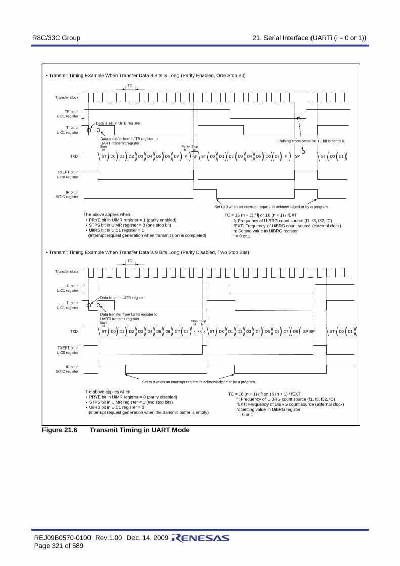
R8C/33C Group 21. Serial Interface (UARTi (i = 0 or 1))
REJ09B0570-0100 Rev.1.00 Dec. 14, 2009Page 321 of 589
Figure 21.6 Transmit Timing in UART Mode
Data is set in UiTB register.
Data is set in UiTB register.
D0
TC
D1 D2 D3 D4 D5 D6 D7 P SPST D0 D1 D2 D3 D4 D5 D6 D7 P SPST D0 D1ST
D0
TC
D1 D2 D3 D4 D5 D6 D7 D8 SP SPST D0 D1 D2 D3 D4 D5 D6 D7 D8 SP SPST D0 D1ST
Transfer clock
TE bit inUiC1 register
TXDi
Set to 0 when an interrupt request is acknowledged or by a program.
• Transmit Timing Example When Transfer Data 8 Bits is Long (Parity Enabled, One Stop Bit)
TC = 16 (n + 1) / fj or 16 (n + 1) / fEXTfj: Frequency of UiBRG count source (f1, f8, f32, fC)fEXT: Frequency of UiBRG count source (external clock)n: Setting value in UiBRG registeri = 0 or 1
The above applies when: • PRYE bit in UiMR register = 1 (parity enabled) • STPS bit in UiMR register = 0 (one stop bit) • UiIRS bit in UiC1 register = 1 (interrupt request generation when transmission is completed)
Startbit
Paritybit
Pulsing stops because TE bit is set to 0.
TXDi
Data transfer from UiTB register toUARTi transmit register
TI bit inUiC1 register
TXEPT bit inUiC0 register
IR bit inSiTIC register
Stopbit
• Transmit Timing Example When Transfer Data is 9 Bits Long (Parity Disabled, Two Stop Bits)
Stopbit
StopbitStart
bit
Transfer clock
TE bit inUiC1 register
TI bit inUiC1 register
TXEPT bit inUiC0 register
IR bit inSiTIC register
Data transfer from UiTB register toUARTi transmit register
TC = 16 (n + 1) / fj or 16 (n + 1) / fEXTfj: Frequency of UiBRG count source (f1, f8, f32, fC)fEXT: Frequency of UiBRG count source (external clock)n: Setting value in UiBRG registeri = 0 or 1
Set to 0 when an interrupt request is acknowledged or by a program.
The above applies when: • PRYE bit in UiMR register = 0 (parity disabled) • STPS bit in UiMR register = 1 (two stop bits) • UiIRS bit in UiC1 register = 0 (interrupt request generation when the transmit buffer is empty)

R8C/33C Group 21. Serial Interface (UARTi (i = 0 or 1))
REJ09B0570-0100 Rev.1.00 Dec. 14, 2009Page 322 of 589
Figure 21.7 Receive Timing in UART Mode
UiBRG output
Set to 0 when an interrupt request is acknowledged or by a program.
• Receive Timing Example When Transfer Data is 8 Bits Long (Parity Disabled, One Stop Bit)
The above applies when :• PRYE bit in UiMR register = 0 (parity disabled)• STPS bit in UiMR register = 0 (one stop bit)
i = 0 or 1
RE bit inUiC1 register
Start bitStop bit
D0 D1 D7RXDi
Transfer clock
“L” is determined.Receive data taken in
Reception starts when a transfer clock isgenerated at the falling edge of the start bit.
Data transfer from UARTi receive register to UiRB register
RI bit inUiC1 register
IR bit inSiRIC register

R8C/33C Group 21. Serial Interface (UARTi (i = 0 or 1))
REJ09B0570-0100 Rev.1.00 Dec. 14, 2009Page 323 of 589
21.4.1 Bit RateIn UART mode, the bit rate is the frequency divided by the UiBRG (i = 0 or 1) register and divided by 16.
Figure 21.8 Formula for Calculating Setting Value in UiBRG (i = 0 or 1) Register
i = 0 or 1Note:
1. For the high-speed on-chip oscillator, the correction value in the FRA4 register should be written into the FRA1 register and the correction value in the FRA5 register should be written into the FRA3 register. This applies when the high-speed on-chip oscillator is selected as the system clock and bits FRA22 to FRA20 in the FRA2 register are set to 000b (divide-by-2 mode). For the precision of the high-speed on-chip oscillator, refer to 32. Electrical Characteristics.
Table 21.8 Bit Rate Setting Example in UART Mode (Internal Clock Selected)
Bit Rate (bps)
UiBRG Count Source
System Clock = 20 MHz System Clock = 18.432 MHz (1) System Clock = 8 MHzUiBRG Setting Value
Actual Time (bps)
Setting Error (%)
UiBRG Setting Value
Actual Time (bps)
Setting Error (%)
UiBRG Setting Value
Actual Time (bps)
Setting Error (%)
1200 f8 129 (81h) 1201.92 0.16 119 (77h) 1200.00 0.00 51 (33h) 1201.92 0.162400 f8 64 (40h) 2403.85 0.16 59 (3Bh) 2400.00 0.00 25 (19h) 2403.85 0.164800 f8 32 (20h) 4734.85 -1.36 29 (1Dh) 4800.00 0.00 12 (0Ch) 4807.69 0.169600 f1 129 (81h) 9615.38 0.16 119 (77h) 9600.00 0.00 51 (33h) 9615.38 0.16
14400 f1 86 (56h) 14367.82 -0.22 79 (4Fh) 14400.00 0.00 34 (22h) 14285.71 -0.7919200 f1 64 (40h) 19230.77 0.16 59 (3Bh) 19200.00 0.00 25 (19h) 19230.77 0.1628800 f1 42 (2Ah) 29069.77 0.94 39 (27h) 28800.00 0.00 16 (10h) 29411.76 2.1238400 f1 32 (20h) 37878.79 -1.36 29 (1Dh) 38400.00 0.00 12 (0Ch) 38461.54 0.1657600 f1 21 (15h) 56818.18 -1.36 19 (13h) 57600.00 0.00 8 (08h) 55555.56 -3.55115200 f1 10 (0Ah) 113636.36 -1.36 9 (09h) 115200.00 0.00 − − −
UART mode
• Internal clock selected
Setting value in UiBRG register = fjBit Rate × 16 − 1
fj: Count source frequency of UiBRG register (f1, f8, f32, or fC)
• External clock selectedfEXT
Bit Rate × 16 − 1
fEXT: Count source frequency of UiBRG register (external clock)
Setting value in UiBRG register =
i = 0 or 1

R8C/33C Group 21. Serial Interface (UARTi (i = 0 or 1))
REJ09B0570-0100 Rev.1.00 Dec. 14, 2009Page 324 of 589
21.4.2 Measure for Dealing with Communication ErrorsIf communication is aborted or a communication error occurs while transmitting or receiving in clocksynchronous serial I/O mode, follow the procedures below:
(1) Set the TE bit in the UiC1 register (i = 0 or 1) to 0 (transmission disabled) and the RE bit to 0 (receptiondisabled).
(2) Set bits SMD2 to SMD0 in the UiMR register to 000b (serial interface disabled).(3) Set bits SMD2 to SMD0 in the UiMR register to 001b (clock synchronous serial I/O mode).(4) Set the TE bit in the UiC1 register to 1 (transmission enabled) and the RE bit to 1 (reception enabled).

R8C/33C Group 21. Serial Interface (UARTi (i = 0 or 1))
REJ09B0570-0100 Rev.1.00 Dec. 14, 2009Page 325 of 589
21.5 Notes on Serial Interface (UARTi (i = 0 or 1))• When reading data from the UiRB (i = 0 or 1) register either in clock synchronous serial I/O mode or in clock
asynchronous serial I/O mode, always read data in 16-bit units. When the high-order byte of the UiRB register is read, bits PER and FER in the UiRB register and the RI bit inthe UiC1 register are set to 0.To check receive errors, read the UiRB register and then use the read data.
Program example to read the receive buffer register:MOV.W 00A6H,R0 ; Read the U0RB register
• When writing data to the UiTB register in clock asynchronous serial I/O mode with 9-bit transfer data length,write data to the high-order byte first and then the low-order byte, in 8-bit units.
Program example to write to the transmit buffer register:MOV.B #XXH,00A3H ; Write to the high-order byte of the U0TB registerMOV.B #XXH,00A2H ; Write to the low-order byte of the U0TB register

R8C/33C Group 22. Serial Interface (UART2)
REJ09B0570-0100 Rev.1.00 Dec. 14, 2009Page 326 of 589
22. Serial Interface (UART2)The serial interface consists of three channels, UART0 to UART2. This chapter describes the UART2.
22.1 OverviewUART2 has a dedicated timer to generate a transfer clock.Figure 22.1 shows a UART2 Block Diagram. Figure 22.2 shows a Block Diagram of UART2 Transmit/ReceiveUnit. Table 22.1 lists the Pin Configuration of UART2.
UART2 has the following modes:
• Clock synchronous serial I/O mode• Clock asynchronous serial I/O mode (UART mode)• Special mode 1 (I2C mode)• Multiprocessor communication function
Figure 22.1 UART2 Block Diagram
n: Setting value in U2BRG register
1/(n+1) 1/16
U2BRGregister
Clock synchronous type(internal clock selected)
Clock synchronous type
Clock synchronous type(internal clock selected)
Clock synchronous type(external clock selected)
CLK2
Clock source selection
f1f8
f32
CKDIRinternal
CKDIRexternal
RTS2
CTS2
Transmit/receive
unit
TXD2
CLKpolarity
switchingcircuit
CTS/RTS disabled
CTS/RTS disabledCTS/RTS selected
Receiveclock
TXDpolarity
switchingcircuit
CLK1 to CLK0= 00b= 01b= 10b
CKPOL
UART reception
UART transmission
Clock synchronous type
CRS = 1
CRS = 0CRD = 0
VSS
CKDIR= 0
CKDIR= 1
SMD2 to SMD0
= 010b, 100b, 101b, 110b
= 001b
CKDIR = 0
SMD2 to SMD0, CKDIR: Bits in U2MR registerCLK1, CLK0, CKPOL, CRD, CRS: Bits in U2C0 registerDF2EN: Bit in URXDF register
CTS2/RTS2
= 11bfC
CKDIR = 1
= 100b, 101b, 110b
= 001b, 010b
1/16
1/2
Transmitclock
CRD = 1
Receptioncontrol circuit
Transmissioncontrol circuit
RXD2
RXD polarityswitching circuit
DF2EN = 1Digital filter
DF2EN = 0

R8C/33C Group 22. Serial Interface (UART2)
REJ09B0570-0100 Rev.1.00 Dec. 14, 2009Page 327 of 589
Figure 22.2 Block Diagram of UART2 Transmit/Receive Unit
Table 22.1 Pin Configuration of UART2Pin Name Assigned Pin I/O FunctionTXD2 P3_4 or P3_7 Output Serial data outputRXD2 P3_4, P3_7, or P4_5 Input Serial data inputCLK2 P3_5 I/O Transfer clock I/OCTS2 P3_3 Input Transmit control input
RTS2 P3_3 Output Receive control inputSCL2 P3_4, P3_7, or P4_5 I/O I2C mode clock I/OSDA2 P3_4 or P3_7 I/O I2C mode data I/O
UART(8 bits)UART(9 bits)
U2ERE = 1
PARdisabled
PARenabled
PRYE = 0
PRYE = 12SPSTPS = 1
1SP
SP SP PAR
UART
UART(7 bits)UART(8 bits)
UART (7 bits)
UART(9 bits)
Clocksynchronous type
Data bus low-order bits
TXD2
UART2 transmit register
D8 D7 D6 D5 D4 D3 D2 D1 D0
SP: Stop bitPAR: Parity bitSMD2 to SMD0, STPS, PRYE, IOPOL, CKDIR: Bits in U2MR registerCLK1, CLK0, CKPOL, CRD, CRS: Bits in U2C0 registerU2ERE: Bit in U2C1 register
U2TBregister
UART(8 bits)UART(9 bits)
I2CClocksynchronous type
U2RBregister
UART2 receive register
PAR
1SP
PARenabled
PARdisabled
UART
UART(7 bits)UART(8 bits)
UART (7 bits)
I2CClocksynchronoustype
Clocksynchronous type
RXD2
Data bus high-order bits
Logic inversion circuit + MSB/LSB conversion circuit
D7 D6 D5 D4 D3 D2 D1 D0D80 0 0 0 0 0 0
Inverted
Not inverted
Error signaloutputcircuit
TXD datainversion
circuitError signal output enabled
Error signal output disabled
Inverted
Not inverted
Logic inversion circuit + MSB/LSB conversion circuit
IOPOL = 0RXD data
inversion circuit
STPS = 0
SP
2SP
PRYE = 0
SMD = 0
IOPOL = 0
I2C
I2C
I2CClocksynchronoustype
IOPOL = 1
SPSTPS = 1 PRYE = 1
UART(9 bits)
I2CClocksynchronoustype
U2ERE = 0
IOPOL = 1
STPS = 0
SMD = 1

R8C/33C Group 22. Serial Interface (UART2)
REJ09B0570-0100 Rev.1.00 Dec. 14, 2009Page 328 of 589
22.2 Registers
22.2.1 UART2 Transmit/Receive Mode Register (U2MR)
22.2.2 UART2 Bit Rate Register (U2BRG)
Write to the U2BRG register while transmission and reception stop. Use the MOV instruction to write to this register.Set bits CLK1 to CLK0 in the U2C0 register before writing to the U2BRG register.
Address 00A8hBit b7 b6 b5 b4 b3 b2 b1 b0
Symbol IOPOL PRYE PRY STPS CKDIR SMD2 SMD1 SMD0After Reset 0 0 0 0 0 0 0 0
Bit Symbol Bit Name Function R/Wb0 SMD0 Serial I/O mode select bit b2 b1 b0
0 0 0: Serial interface disabled 0 0 1: Clock synchronous serial I/O mode 0 1 0: I2C mode 1 0 0: UART mode, transfer data 7 bits long 1 0 1: UART mode, transfer data 8 bits long 1 1 0: UART mode, transfer data 9 bits longOther than above: Do not set.
R/Wb1 SMD1 R/Wb2 SMD2 R/W
b3 CKDIR Internal/external clock select bit 0: Internal clock1: External clock
R/W
b4 STPS Stop bit length select bit 0: One stop bit1: Two stop bits
R/W
b5 PRY Odd/even parity select bit Enabled when PRYE = 10: Odd parity1: Even parity
R/W
b6 PRYE Parity enable bit 0: Parity disabled1: Parity enabled
R/W
b7 IOPOL TXD, RXD I/O polarity switch bit 0: Not inverted1: Inverted
R/W
Address 00A9hBit b7 b6 b5 b4 b3 b2 b1 b0
Symbol — — — — — — — —After Reset X X X X X X X X
Bit Function Setting Range R/Wb7 to b0 If the setting value is n, U2BRG divides the count source by n+1. 00h to FFh W

R8C/33C Group 22. Serial Interface (UART2)
REJ09B0570-0100 Rev.1.00 Dec. 14, 2009Page 329 of 589
22.2.3 UART2 Transmit Buffer Register (U2TB)
Note:1. Set bits b0 to b7 after setting the MPTB bit.
Address 00ABh to 00AAhBit b7 b6 b5 b4 b3 b2 b1 b0
Symbol — — — — — — — —After Reset X X X X X X X X
Bit b15 b14 b13 b12 b11 b10 b9 b8Symbol — — — — — — — MPTB
After Reset X X X X X X X X
Bit Symbol Function R/Wb0 — Transmit data (D7 to D0) Wb1 —b2 —b3 —b4 —b5 —b6 —b7 —b8 MPTB Transmit data (D8) (1)
[When the multiprocessor communication function is not used]Transmit data (D8)[When the multiprocessor communication function is used]• To transfer an ID, set the MPTB bit to 1. • To transfer data, set the MPTB bit to 0.
W
b9 — Nothing is assigned. If necessary, set to 0. When read, the content is 0. —b10 —b11 —b12 —b13 —b14 —b15 —

R8C/33C Group 22. Serial Interface (UART2)
REJ09B0570-0100 Rev.1.00 Dec. 14, 2009Page 330 of 589
22.2.4 UART2 Transmit/Receive Control Register 0 (U2C0)
Notes:1. If bits CLK1 to CLK0 are switched, set the U2BRG register again.2. The UFORM bit is enabled when bits SMD2 to SMD0 in the U2MR register are set to 001b (clock synchronous
serial I/O mode), or set to 101b (UART mode, transfer data 8 bits long).Set the UFORM bit to 1 when bits SMD2 to SMD0 are set to 010b (I2C mode), and to 0 when bits SMD2 to SMD0are set to 100b (UART mode, transfer data 7 bits long) or 110b (UART mode, transfer data 9 bits long).
Address 00AChBit b7 b6 b5 b4 b3 b2 b1 b0
Symbol UFORM CKPOL NCH CRD TXEPT CRS CLK1 CLK0After Reset 0 0 0 0 1 0 0 0
Bit Symbol Bit Name Function R/Wb0 CLK0 U2BRG count source
select bit (1)b1 b0 0 0: f1 selected 0 1: f8 selected 1 0: f32 selected 1 1: fC selected
R/Wb1 CLK1 R/W
b2 CRS CTS/RTS function select bit Enabled when CRD = 00: CTS function selected1: RTS function selected
R/W
b3 TXEPT Transmit register empty flag 0: Data present in the transmit register (transmission in progress)
1: No data in the transmit register (transmission completed)
R
b4 CRD CTS/RTS disable bit 0: CTS/RTS function enabled1: CTS/RTS function disabled
R/W
b5 NCH Data output select bit 0: Pins TXD2/SDA2, SCL2 set to CMOS output1: Pins TXD2/SDA2, SCL2 set to N-channel open-drain
output
R/W
b6 CKPOL CLK polarity select bit 0: Transmit data output at the falling edge and receive data input at the rising edge of the transfer clock
1: Transmit data output at the rising edge and receive data input at the falling edge of the transfer clock
R/W
b7 UFORM Transfer format select bit (2) 0: LSB first1: MSB first
R/W

R8C/33C Group 22. Serial Interface (UART2)
REJ09B0570-0100 Rev.1.00 Dec. 14, 2009Page 331 of 589
22.2.5 UART2 Transmit/Receive Control Register 1 (U2C1)
Note:1. The U2LCH bit is enabled when bits SMD2 to SMD0 in the U2MR register are set to 001b (clock synchronous
serial I/O mode), 100b (UART mode, transfer data 7 bits long), or 101b (UART mode, transfer data 8 bits long). Set the U2LCH bit to 0 when bits SMD2 to SMD0 are set to 010b (I2C mode) or 110b (UART mode, transfer data9 bits long).
Address 00ADhBit b7 b6 b5 b4 b3 b2 b1 b0
Symbol U2ERE U2LCH U2RRM U2IRS RI RE TI TEAfter Reset 0 0 0 0 0 0 1 0
Bit Symbol Bit Name Function R/Wb0 TE Transmit enable bit 0: Transmission disabled
1: Transmission enabledR/W
b1 TI Transmit buffer empty flag 0: Data present in the U2TB register1: No data in the U2TB register
R
b2 RE Receive enable bit 0: Reception disabled1: Reception enabled
R/W
b3 RI Receive complete flag 0: No data in the U2RB register1: Data present in the U2RB register
R
b4 U2IRS UART2 transmit interrupt source select bit
0: Transmit buffer empty (TI = 1)1: Transmission completed (TXEPT = 1)
R/W
b5 U2RRM UART2 continuous receive mode enable bit
0: Continuous receive mode disabled1: Continuous receive mode enabled
R/W
b6 U2LCH Data logic select bit (1) 0: Not inverted1: Inverted
R/W
b7 U2ERE Error signal output enable bit 0: Output disabled1: Output enabled
R/W

R8C/33C Group 22. Serial Interface (UART2)
REJ09B0570-0100 Rev.1.00 Dec. 14, 2009Page 332 of 589
22.2.6 UART2 Receive Buffer Register (U2RB)
Notes:1. When bits SMD2 to SMD0 in the U2MR register are set to 000b (serial interface disabled) or the RE bit in the
U2C1 register is set to 0 (reception disabled), all of bits SUM, PER, FER, and OER are set to 0 (no error). TheSUM bit is set to 0 (no error) when all of bits PER, FER, and OER are set to 0 (no error). Bits PER and FER areset to 0 by reading the lower byte of the U2RB register.When setting bits SMD2 to SMD0 in the U2MR register to 000b, set the TE bit in the U2C1 register to 0(transmission disabled) and the RE bit to 0 (reception disabled).
2. These error flags are disabled when bits SMD2 to SMD0 in the U2MR register are set to 001b (clocksynchronous serial I/O mode) or to 010b (I2C mode). When read, the content is undefined.
Address 00AFh to 00AEhBit b7 b6 b5 b4 b3 b2 b1 b0
Symbol — — — — — — — —After Reset X X X X X X X X
Bit b15 b14 b13 b12 b11 b10 b9 b8Symbol SUM PER FER OER — — — MPRB
After Reset X X X X X X X X
Bit Symbol Bit Name Function R/Wb0 — — Receive data (D7 to D0) Rb1 —b2 —b3 —b4 —b5 —b6 —b7 —b8 MPRB — Receive data (D8) (1)
[When the multiprocessor communication function is not used]Receive data (D8)[When the multiprocessor communication function is used]• When the MPRB bit is set to 0, received D0 to D7
are data fields.• When the MPRB bit is set to 1, received D0 to D7
are ID fields.
R
b9 — Nothing is assigned. If necessary, set to 0. When read, the content is undefined. —b10 —b11 — Reserved bit Set to 0. R/Wb12 OER Overrun error flag (1) 0: No overrun error
1: Overrun errorR
b13 FER Framing error flag (1, 2) 0: No framing error1: Framing error
R
b14 PER Parity error flag (1, 2) 0: No parity error1: Parity error
R
b15 SUM Error sum flag (1, 2) 0: No error1: Error
R

R8C/33C Group 22. Serial Interface (UART2)
REJ09B0570-0100 Rev.1.00 Dec. 14, 2009Page 333 of 589
22.2.7 UART2 Digital Filter Function Select Register (URXDF)
Note:1. The RXD2 digital filter can be used only in clock asynchronous serial I/O (UART) mode. When bits SMD2 to
SMD0 in the U2MR register are set to 001b (clock synchronous serial I/O mode) or 010b (I2C mode), set theDF2EN bit to 0 (RXD2 digital filter disabled).
22.2.8 UART2 Special Mode Register 5 (U2SMR5)
Note:1. When the MP bit is set to 1 (multiprocessor communication enabled), the settings of bits PRY and PRYE in the
U2MR register are disabled. If bits SMD2 to SMD0 in the U2MR register are set to 001b (clock synchronousserial I/O mode), set the MP bit to 0 (multiprocessor communication disabled).
Address 00B0hBit b7 b6 b5 b4 b3 b2 b1 b0
Symbol — — — — — DF2EN — —After Reset 0 0 0 0 0 0 0 0
Bit Symbol Bit Name Function R/Wb0 — Nothing is assigned. If necessary, set to 0. When read, the content is 0. —b1 —b2 DF2EN RXD2 digital filter enable bit (1) 0: RXD2 digital filter disabled
1: RXD2 digital filter enabledR/W
b3 — Nothing is assigned. If necessary, set to 0. When read, the content is 0. —b4 —b5 —b6 —b7 —
Address 00BBhBit b7 b6 b5 b4 b3 b2 b1 b0
Symbol — — — MPIE — — — MPAfter Reset 0 0 0 0 0 0 0 0
Bit Symbol Bit Name Function R/Wb0 MP Multiprocessor communication
enable bit0: Multiprocessor communication disabled1: Multiprocessor communication enabled (1)
R/W
b1 — Nothing is assigned. If necessary, set to 0. When read, the content is 0. —b2 —b3 —b4 MPIE Multiprocessor communication
control bitThis bit is enabled when the MP bit is set to 1 (multiprocessor communication enabled).When the MPIE bit is set to 1, the following will result:• Receive data in which the multiprocessor bit is 0
is ignored. Setting of the RI bit in the U2C1 register and bits OER and FER in the U2RB register to 1 is disabled.
• On receiving receive data in which the multiprocessor bit is 1, the MPIE bit is set to 0 and receive operation other than multiprocessor communication is performed.
R/W
b5 — Nothing is assigned. If necessary, set to 0. When read, the content is 0. —b6 —b7 — Reserved bit Set to 0. R/W

R8C/33C Group 22. Serial Interface (UART2)
REJ09B0570-0100 Rev.1.00 Dec. 14, 2009Page 334 of 589
22.2.9 UART2 Special Mode Register 4 (U2SMR4)
Note:1. This bit is set to 0 when each condition is generated.
22.2.10 UART2 Special Mode Register 3 (U2SMR3)
Notes:1. Bits DL2 to DL0 are used to generate a delay in SDA2 output digitally in I2C mode. In other than I2C mode, set
these bits to 000b (no delay).2. The amount of delay varies with the load on pins SCL2 and SDA2. When an external clock is used, the amount
of delay increases by about 100 ns.
Address 00BChBit b7 b6 b5 b4 b3 b2 b1 b0
Symbol SWC9 SCLHI ACKC ACKD STSPSEL STPREQ RSTAREQ STAREQAfter Reset 0 0 0 0 0 0 0 0
Bit Symbol Bit Name Function R/Wb0 STAREQ Start condition generate bit (1) 0: Clear
1: StartR/W
b1 RSTAREQ Restart condition generate bit (1) 0: Clear1: Start
R/W
b2 STPREQ Stop condition generate bit (1) 0: Clear1: Start
R/W
b3 STSPSEL SCL, SDA output select bit 0: Start and stop conditions not output1: Start and stop conditions output
R/W
b4 ACKD ACK data bit 0: ACK1: NACK
R/W
b5 ACKC ACK data output enable bit 0: Serial interface data output1: ACK data output
R/W
b6 SCLHI SCL output stop enable bit 0: Disabled1: Enabled
R/W
b7 SWC9 SCL wait bit 3 0: SCL “L” hold disabled1: SCL “L” hold enabled
R/W
Address 00BDhBit b7 b6 b5 b4 b3 b2 b1 b0
Symbol DL2 DL1 DL0 — NODC — CKPH —After Reset 0 0 0 X 0 X 0 X
Bit Symbol Bit Name Function R/Wb0 — Nothing is assigned. If necessary, set to 0. When read, the content is undefined. —b1 CKPH Clock phase set bit 0: No clock delay
1: With clock delayR/W
b2 — Nothing is assigned. If necessary, set to 0. When read, the content is undefined. —b3 NODC Clock output select bit 0: CLK2 set to CMOS output
1: CLK2 set to N-channel open-drain outputR/W
b4 — Nothing is assigned. If necessary, set to 0. When read, the content is undefined. —b5 DL0 SDA2 digital delay setup bit (1, 2) b7 b6 b5
0 0 0: No delay 0 0 1: 1 to 2 cycle(s) of U2BRG count source 0 1 0: 2 to 3 cycles of U2BRG count source 0 1 1: 3 to 4 cycles of U2BRG count source 1 0 0: 4 to 5 cycles of U2BRG count source 1 0 1: 5 to 6 cycles of U2BRG count source 1 1 0: 6 to 7 cycles of U2BRG count source 1 1 1: 7 to 8 cycles of U2BRG count source
R/Wb6 DL1 R/Wb7 DL2 R/W

R8C/33C Group 22. Serial Interface (UART2)
REJ09B0570-0100 Rev.1.00 Dec. 14, 2009Page 335 of 589
22.2.11 UART2 Special Mode Register 2 (U2SMR2)
22.2.12 UART2 Special Mode Register (U2SMR)
Note:1. The BBS bit is set to 0 by writing 0 by a program (Writing 1 has no effect).
Address 00BEhBit b7 b6 b5 b4 b3 b2 b1 b0
Symbol — SDHI SWC2 STAC — SWC CSC IICM2After Reset X 0 0 0 0 0 0 0
Bit Symbol Bit Name Function R/Wb0 IICM2 I2C mode select bit 2 Refer to Table 22.12 I2C Mode Functions. R/Wb1 CSC Clock synchronization bit 0: Disabled
1: EnabledR/W
b2 SWC SCL wait output bit 0: Disabled1: Enabled
R/W
b3 — Reserved bit Set to 0. R/Wb4 STAC UART2 initialization bit 0: Disabled
1: EnabledR/W
b5 SWC2 SCL wait output bit 2 0: Transfer clock1: “L” output
R/W
b6 SDHI SDA output disable bit 0: Enabled1: Disabled (high-impedance)
R/W
b7 — Nothing is assigned. If necessary, set to 0. When read, the content is undefined. —
Address 00BFhBit b7 b6 b5 b4 b3 b2 b1 b0
Symbol — — — — — BBS — IICMAfter Reset X 0 0 0 0 0 0 0
Bit Symbol Bit Name Function R/Wb0 IICM I2C mode select bit 0: Other than I2C mode
1: I2C modeR/W
b1 — Reserved bit Set to 0. R/Wb2 BBS Bus busy flag (1) 0: Stop condition detected
1: Start condition detected (busy)R/W
b3 — Reserved bit Set to 0. R/Wb4 — R/Wb5 — R/Wb6 — R/Wb7 — Nothing is assigned. If necessary, set to 0. When read, the content is undefined. —

R8C/33C Group 22. Serial Interface (UART2)
REJ09B0570-0100 Rev.1.00 Dec. 14, 2009Page 336 of 589
22.2.13 UART2 Pin Select Register 0 (U2SR0)
The U2SR0 register selects which pin is assigned to the UART2 I/O. To use the I/O pin for UART2, set thisregister. Set the U2SR0 register before setting the UART2 associated registers. Also, do not change the setting value inthis register during UART2 operation.
22.2.14 UART2 Pin Select Register 1 (U2SR1)
The U2SR1 register selects which pin is assigned to the UART2 I/O. To use the I/O pin for UART2, set thisregister. Set the U2SR1 register before setting the UART2 associated registers. Also, do not change the setting value inthis register during UART2 operation.
Address 018AhBit b7 b6 b5 b4 b3 b2 b1 b0
Symbol — — RXD2SEL1 RXD2SEL0 — — TXD2SEL1 TXD2SEL0After Reset 0 0 0 0 0 0 0 0
Bit Symbol Bit Name Function R/Wb0 TXD2SEL0 TXD2/SDA2 pin select bit b1 b0
0 0: TXD2/SDA2 pin not used 0 1: P3_7 assigned 1 0: P3_4 assigned 1 1: Do not set.
R/Wb1 TXD2SEL1 R/W
b2 — Reserved bit Set to 0. R/Wb3 — Nothing is assigned. If necessary, set to 0. When read, the content is 0. —b4 RXD2SEL0 RXD2/SCL2 pin select bit b5 b4
0 0: RXD2/SCL2 pin not used 0 1: P3_4 assigned 1 0: P3_7 assigned 1 1: P4_5 assigned
R/Wb5 RXD2SEL1 R/W
b6 — Reserved bit Set to 0. R/Wb7 — Nothing is assigned. If necessary, set to 0. When read, the content is 0. —
Address 018BhBit b7 b6 b5 b4 b3 b2 b1 b0
Symbol — — — CTS2SEL0 — — — CLK2SEL0After Reset 0 0 0 0 0 0 0 0
Bit Symbol Bit Name Function R/Wb0 CLK2SEL0 CLK2 pin select bit 0: CLK2 pin not used
1: P3_5 assignedR/W
b1 — Reserved bit Set to 0. R/Wb2 — Nothing is assigned. If necessary, set to 0. When read, the content is 0. —b3 —b4 CTS2SEL0 CTS2/RTS2 pin select bit 0: CTS2/RTS2 pin not used
1: P3_3 assignedR/W
b5 — Reserved bit Set to 0. R/Wb6 — Nothing is assigned. If necessary, set to 0. When read, the content is 0. —b7 —

R8C/33C Group 22. Serial Interface (UART2)
REJ09B0570-0100 Rev.1.00 Dec. 14, 2009Page 337 of 589
22.3 Clock Synchronous Serial I/O ModeIn clock synchronous serial I/O mode, data is transmitted and received using a transfer clock.Table 22.2 lists the Clock Synchronous Serial I/O Mode Specifications. Table 22.3 lists the Registers Used andSettings in Clock Synchronous Serial I/O Mode.
Notes:1. When an external clock is selected, the requirements must be met in either of the following states:
- The external clock is held high when the CKPOL bit in the U2C0 register is set to 0 (transmit data output at the falling edge and receive data input at the rising edge of the transfer clock)
- The external clock is held low when the CKPOL bit in the U2C0 register is set to 1 (transmit data output at the rising edge and receive data input at the falling edge of the transfer clock)
2. If an overrun error occurs, the receive data in the U2RB register will be undefined. The IR bit in the S2RICregister does not change to 1 (interrupt requested).
Table 22.2 Clock Synchronous Serial I/O Mode SpecificationsItem Specification
Transfer data format Transfer data length: 8 bitsTransfer clock • The CKDIR bit in the U2MR register is set to 0 (internal clock): fj/(2(n+1))
fj = f1, f8, f32, fC n = setting value in the U2BRG register: 00h to FFh• The CKDIR bit is set to 1 (external clock): Input from the CLK2 pin
Transmit/receive control Selectable from the CTS function, RTS function, or CTS/RTS function disabled.Transmit start conditions To start transmission, the following requirements must be met: (1)
• The TE bit in the U2C1 register is set to 1 (transmission enabled)• The TI bit in the U2C1 register is set to 0 (data present in the U2TB register)• If the CTS function is selected, input to the CTS2 pin = “L”.
Receive start conditions To start reception, the following requirements must be met: (1)
• The RE bit in the U2C1 register is set to 1 (reception enabled).• The TE bit in the U2C1 register is set to 1 (transmission enabled).• The TI bit in the U2C1 register is set to 0 (data present in the U2TB register).
Interrupt request generation timing
For transmission, one of the following conditions can be selected.• The U2IRS bit in the U2C1 register is set to 0 (transmit buffer empty):
When data is transferred from the U2TB register to the UART2 transmit register (at start of transmission).
• The U2IRS bit is set to 1 (transmission completed): When data transmission from the UART2 transmit register is completed.
For reception• When data is transferred from the UART2 receive register to the U2RB register
(at completion of reception).Error detection Overrun error (2)
This error occurs if the serial interface starts receiving the next unit of data before reading the U2RB register and receives the 7th bit of the next unit of data.
Selectable functions • CLK polarity selectionTransfer data I/O can be selected to occur synchronously with the rising or fallingedge of the transfer clock.
• LSB first, MSB first selectionWhether transmitting or receiving data begins with bit 0 or begins with bit 7 can beselected.
• Continuous receive mode selectionReception is enabled immediately by reading the U2RB register.
• Serial data logic switchingThis function inverts the logic value of the transmit/receive data.

R8C/33C Group 22. Serial Interface (UART2)
REJ09B0570-0100 Rev.1.00 Dec. 14, 2009Page 338 of 589
Note:1. Set the bits not listed in this table to 0 when writing to the above registers in clock synchronous
serial I/O mode.
Table 22.3 Registers Used and Settings in Clock Synchronous Serial I/O ModeRegister Bit Function
U2TB (1) b0 to b7 Set transmit data.U2RB (1) b0 to b7 Receive data can be read.
OER Overrun error flagU2BRG b0 to b7 Set a bit rate.U2MR (1) SMD2 to SMD0 Set to 001b.
CKDIR Select the internal clock or external clock.IOPOL Set to 0.
U2C0 CLK1, CLK0 Select the count source for the U2BRG register.CRS Select either CTS or RTS to use functions.TXEPT Transmit register empty flagCRD Enable or disable the CTS or RTS function.NCH Select TXD2 pin output mode.CKPOL Select the transfer clock polarity.UFORM Select LSB first or MSB first.
U2C1 TE Set to 1 to enable transmission/reception.TI Transmit buffer empty flagRE Set to 1 to enable reception.RI Receive complete flagU2IRS Select the source of UART2 transmit interrupt.U2RRM Set to 1 to use continuous receive mode.U2LCH Set to 1 to use inverted data logic.U2ERE Set to 0.
U2SMR b0 to b7 Set to 0.U2SMR2 b0 to b7 Set to 0.U2SMR3 b0 to b2 Set to 0.
NODC Select clock output mode.b4 to b7 Set to 0.
U2SMR4 b0 to b7 Set to 0.URXDF DF2EN Set to 0.U2SMR5 MP Set to 0.

R8C/33C Group 22. Serial Interface (UART2)
REJ09B0570-0100 Rev.1.00 Dec. 14, 2009Page 339 of 589
Table 22.4 lists the Pin Functions in Clock Synchronous Serial I/O Mode (Multiple Transfer Clock Output PinFunction Not Selected). Note that for a period from when UART2 operating mode is selected to when transfer starts, the TXD2 pin outputsa “H” level. (When N-channel open-drain output is selected, this pin is in the high-impedance state.)Figure 22.3 shows the Transmit and Receive Timing in Clock Synchronous Serial I/O Mode.
Table 22.4 Pin Functions in Clock Synchronous Serial I/O Mode (Multiple Transfer Clock Output Pin Function Not Selected)
Pin Name Function Selection MethodTXD2(P3_4 or P3_7)
Serial data output • TXD2 (P3_4)Bits TXD2SEL1 to TXD2SEL0 in U2SR0 register = 10b (P3_4)
• TXD2 (P3_7)Bits TXD2SEL1 to TXD2SEL0 in U2SR0 register = 01b (P3_7)
• For reception only:P3_4 and P3_7 can be used as ports by setting TXD2SEL1 toTXD2SEL0 to 00b.
RXD2(P3_4, P3_7, orP4_5)
Serial data input • RXD2 (P3_4)Bits RXD2SEL1 to RXD2SEL0 in U2SR0 register = 01b (P3_4)PD3_4 bit in PD3 register = 0
• RXD2 (P3_7)Bits RXD2SEL1 to RXD2SEL0 in U2SR0 register = 10b (P3_7)PD3_7 bit in PD3 register = 0
• RXD2 (P4_5)Bits RXD2SEL1 to RXD2SEL0 in U2SR0 register = 11b (P4_5)PD4_5 bit in PD4 register = 0
• For transmission only:P3_4, P3_7, and P4_5 can be used as ports by settingRXD2SEL1 to RXD2SEL0 to 00b.
CLK2 (P3_5) Transfer clock output CLK2SEL0 bit in U2SR1 register = 1CKDIR bit in U2MR register = 0
Transfer clock input CLK2SEL0 bit in U2SR1 register = 1CKDIR bit in U2MR register = 1PD3_5 bit in PD3 register = 0
CTS2/RTS2(P3_3)
CTS input CTS2SEL0 bit in U2SR1 register = 1CRD bit in U2C0 register = 0CRS bit in U2C0 register = 0PD3_3 bit in PD3 register = 0
RTS output CTS2SEL0 bit in U2SR1 register = 1CRD bit in U2C0 register = 0CRS bit in U2C0 register = 1
I/O port CTS2SEL0 bit in U2SR1 register = 0

R8C/33C Group 22. Serial Interface (UART2)
REJ09B0570-0100 Rev.1.00 Dec. 14, 2009Page 340 of 589
Figure 22.3 Transmit and Receive Timing in Clock Synchronous Serial I/O Mode
D0 D1 D2 D3 D4 D5 D6 D7 D0 D1 D2 D3 D4 D5 D6 D7 D0 D1 D2 D3 D4 D5 D6 D7
TC
TCLKPulsing stops because TE bit is set to 0.
Data is set in U2TB register.
Data transfer from U2TB register to UART2 transmit register
TC = TCLK = 2(n+1)/fjfj: Frequency of U2BRG count source
(f1, f8, f32, fC)n: Setting value in U2BRG register
Transfer clock
TE bit inU2C1 register
TI bit inU2C1 register
CLK2
TXD2
TXEPT flag inU2C0 register
CTS2
IR bit inS2TIC register
Set to 0 when an interrupt request is acknowledged or by a program.
Pulsing stops because “H” is applied to CTS2.
1/fEXT
Dummy data is set in U2TB register.
CLK2
RXD2
RTS2
RE bit inU2C1 register
Data transfer from U2TB register to UART2 transmit register
Data read from U2RB register
fEXT: Frequency of external clock
Make sure the following conditions are metwhen the CLK2 pin input before receiving data is high:
• TE bit in U2C0 register = 1 (transmission enabled)• RE bit in U2C1 register = 1 (reception enabled)• Dummy data is written to U2TB register
Data transfer from UART2 receiveregister to U2RB register
Set to 0 when an interrupt request is acknowledged or by a program.
D0 D1 D2 D3 D4 D5 D6 D7 D0 D1 D2 D3 D4 D5 D0 D1 D2 D3 D4 D5D7D6 D6
TE bit inU2C1 register
TI bit inU2C1 register
OER flag inU2RB register
IR bit inS2RIC register
RI bit inU2C1 register
The above applies when:• CKDIR bit in U2MR register = 0 (internal clock)• CRD bit in U2C0 register = 0 (CTS/RTS function enabled), CRS bit = 0 (CTS function selected)• CKPOL bit in U2C0 register = 0 (transmit data output at the falling edge and receive data input at the rising edge of the transfer clock)• U2IRS bit in U2C1 register = 0 (interrupt request generation when the U2TB register is empty)
The above applies when:• CKDIR bit in U2MR register = 1 (external clock)• CRD bit in U2C0 register = 0 (CTS/RTS function enabled), CRS bit = 1 (RTS function selected)• CKPOL bit in U2C0 register = 0 (transmit data output at the falling edge and receive data input at the rising edge of the transfer clock)
Received data taken in
“L” is applied when U2RB register is read.
(1) Transmit Timing Example (Internal Clock Selected)
(2) Receive Timing Example (External Clock Selected)

R8C/33C Group 22. Serial Interface (UART2)
REJ09B0570-0100 Rev.1.00 Dec. 14, 2009Page 341 of 589
22.3.1 Measure for Dealing with Communication ErrorsIf communication is aborted or a communication error occurs while transmitting or receiving in clocksynchronous serial I/O mode, follow the procedures below:
(1) Set the TE bit in the U2C1 register to 0 (transmission disabled) and the RE bit to 0 (reception disabled).(2) Set bits SMD2 to SMD0 in the U2MR register to 000b (serial interface disabled).(3) Set bits SMD2 to SMD0 in the U2MR register to 001b (clock synchronous serial I/O mode).(4) Set the TE bit in the U2C1 register to 1 (transmission enabled) and the RE bit to 1 (reception enabled).
22.3.2 CLK Polarity Select FunctionUse the CKPOL bit in the U2C0 register to select the transfer clock polarity. Figure 22.4 shows the TransferClock Polarity.
Figure 22.4 Transfer Clock Polarity
(2) CKPOL bit in U2C0 register = 1 (transmit data output at the rising edge andreceive data input at the falling edge of the transfer clock)
D1 D2 D3 D4 D5 D6 D7
D1 D2 D3 D4 D5 D6 D7
D0
D0
TXD2
RXD2
CLK2
(1) CKPOL bit in U2C0 register = 0 (transmit data output at the falling edge and receive data input at the rising edge of the transfer clock)
D1 D2 D3 D4 D5 D6 D7D0
D1 D2 D3 D4 D5 D6 D7D0
TXD2
RXD2
CLK2
The above applies when:• UFORM bit in U2C0 register = 0 (LSB first)• U2LCH bit in U2C1 register = 0 (not inverted)
“H” output from CLK2 pin during no transfer
“L” output from CLK2 pin during no transfer

R8C/33C Group 22. Serial Interface (UART2)
REJ09B0570-0100 Rev.1.00 Dec. 14, 2009Page 342 of 589
22.3.3 LSB First/MSB First Select FunctionUse the UFORM bit in the U2C0 register to select the transfer format. Figure 22.5 shows the Transfer Format.
Figure 22.5 Transfer Format
22.3.4 Continuous Receive ModeIn continuous receive mode, receive operation is enabled when the receive buffer register is read. It is notnecessary to write dummy data to the transmit buffer register to enable receive operation in this mode.However, a dummy read of the receive buffer register is required when starting the operating mode.When the U2RRM bit in the U2C1 register is set to 1 (continuous receive mode), the TI bit in the U2C1 registeris set to 0 (data present in the U2TB register) by reading the U2RB register. If the U2RRM bit is set to 1, do notwrite dummy data to the U2TB register by a program.
(1) UFORM Bit in U2C0 Register = 0 (LSB first)
D1 D2 D3 D4 D5 D6 D7D0
D1 D2 D3 D4 D5 D6 D7D0
TXD2
RXD2
CLK2
(2) UFORM Bit in U2C0 Register = 1 (MSB first)
D6 D5 D4 D3 D2 D1 D0D7
D6 D5 D4 D3 D2 D1 D0D7
TXD2
RXD2
CLK2
The above applies when:• CKPOL bit in U2C0 register = 0
(transmit data output at the falling edge and receive data input at the rising edge of the transfer clock)
• U2LCH bit in U2C1 register = 0 (not inverted)

R8C/33C Group 22. Serial Interface (UART2)
REJ09B0570-0100 Rev.1.00 Dec. 14, 2009Page 343 of 589
22.3.5 Serial Data Logic Switching FunctionIf the U2LCH bit in the U2C1 register is set to 1 (inverted), the data written to the U2TB register has its logicinverted before being transmitted. Similarly, the received data has its logic inverted when read from the U2RBregister. Figure 22.6 shows the Serial Data Logic Switching.
Figure 22.6 Serial Data Logic Switching
22.3.6 CTS/RTS FunctionThe CTS function is used to start transmit and receive operation when “L” is applied to the CTS2/RTS2 pin.Transmit and receive operation begins when the CTS2/RTS2 pin is held low. If the “L” signal is switched to“H” during a transmit or receive operation, the operation stops before the next data.For the RTS function, the CTS2/RTS2 pin outputs “L” when the MCU is ready for a receive operation. Theoutput level goes high at the first falling edge of the CLK2 pin.• The CRD bit in the U2C0 register = 1 (CTS/RTS function disabled)
The CTS2/RTS2 pin operates as the programmable I/O function.• The CRD bit = 0, CRS bit = 0 (CTS function selected)
The CTS2/RTS2 pin operates as the CTS function.• The CRD bit = 0, CRS bit = 1 (RTS function selected)
The CTS2/RTS2 pin operates as the RTS function.
D0 D1 D2 D3 D4 D5 D6 D7
Transfer Clock
TXD2(not inverted)
(1) U2LCH Bit in U2C1 Register = 0 (not inverted)
(2) U2LCH Bit in U2C1 Register = 1 (inverted)
The above applies when:• CKPOL bit in U2C0 register = 0 (transmit data output at the falling edge of the transfer clock)• UFORM bit in U2C0 register = 0 (LSB first)
D0 D1 D2 D3 D4 D5 D6 D7
Transfer Clock
TXD2(inverted)

R8C/33C Group 22. Serial Interface (UART2)
REJ09B0570-0100 Rev.1.00 Dec. 14, 2009Page 344 of 589
22.4 Clock Asynchronous Serial I/O (UART) ModeIn UART mode, data is transmitted and received after setting the desired bit rate and transfer data format. Table22.5 lists the UART Mode Specifications. Table 22.6 lists the Registers Used and Settings in UART Mode.
Notes:1. If an overrun error occurs, the receive data in the U2RB register will be undefined. The IR bit in the S2RIC
register remains unchanged.2. The framing error flag and the parity error flag are set to 1 when data is transferred from the UART2 receive
register to the U2RB register.
Table 22.5 UART Mode SpecificationsItem Specification
Transfer data format • Character bits (transfer data): Selectable from 7, 8, or 9 bits• Start bit:1 bit• Parity bit: Selectable from odd, even, or none• Stop bits: Selectable from 1 bit or 2 bits
Transfer clock • The CKDIR bit in the U2MR register is set to 0 (internal clock): fj/(16(n + 1))fj = f1, f8, f32, fC n = setting value in the U2BRG register: 00h to FFh
• The CKDIR bit is set to 1 (external clock): fEXT/(16(n + 1))fEXT: Input from CLK2 pin n: Setting value in the U2BRG register: 00h to FFh
Transmit/receive control Selectable from the CTS function, RTS function, or CTS/RTS function disabled.Transmit start conditions To start transmission, the following requirements must be met:
• The TE bit in the U2C1 register is set to 1 (transmission enabled).• The TI bit in the U2C1 register is set to 0 (data present in the U2TB register).• If the CTS function is selected, input to the CTS2 pin = “L”.
Receive start conditions To start reception, the following requirements must be met:• The RE bit in the U2C1 register is set to 1 (reception enabled).• Start bit detection
Interrupt request generation timing
For transmission, one of the following conditions can be selected.• The U2IRS bit in the U2C1 register is set to 0 (transmit buffer empty):
When data is transferred from the U2TB register to the UART2 transmit register (at start of transmission).
• The U2IRS bit is set to 1 (transmission completed): When data transmission from the UART2 transmit register is completed.
For reception• When data is transferred from the UART2 receive register to the U2RB register
(at completion of reception).Error detection • Overrun error (1)
This error occurs if the serial interface starts receiving the next unit of data beforereading the U2RB register and receives the bit one before the last stop bit of thenext unit of data.
• Framing error (2)
This error occurs when the set number of stop bits is not detected.• Parity error (2)
This error occurs when if parity is enabled, the number of 1’s in the parity andcharacter bits does not match the set number of 1’s.
• Error sum flagThis flag is set to 1 if an overrun, framing, or parity error occurs.
Selectable functions • LSB first, MSB first selectionWhether transmitting or receiving data begins with bit 0 or begins with bit 7 can beselected.
• Serial data logic switchingThis function inverts the logic of the transmit/receive data. The start and stop bitsare not inverted.
• TXD, RXD I/O polarity switchingThis function inverts the polarities of the TXD pin output and RXD pin input. Thelogic levels of all I/O data are inverted.
• RXD2 digital filter selectionThe RXD2 input signal can be enabled or disabled.

R8C/33C Group 22. Serial Interface (UART2)
REJ09B0570-0100 Rev.1.00 Dec. 14, 2009Page 345 of 589
Notes:1. The bits used for transmit/receive data are as follows:
- Bits b0 to b6 when transfer data is 7 bits long - Bits b0 to b7 when transfer data is 8 bits long- Bits b0 to b8 when transfer data is 9 bits long
2. The contents of the following are undefined: - Bits b7 and b8 when transfer data is 7 bits long - Bit b8 when transfer data is 8 bits long
Table 22.6 Registers Used and Settings in UART ModeRegister Bit Function
U2TB b0 to b8 Set transmit data. (1)
U2RB b0 to b8 Receive data can be read. (1, 2)
OER, FER, PER, SUM Error flagU2BRG b0 to b7 Set a bit rate.U2MR SMD2 to SMD0 Set to 100b when transfer data is 7 bits long.
Set to 101b when transfer data is 8 bits long.Set to 110b when transfer data is 9 bits long.
CKDIR Select the internal clock or external clock.STPS Select the stop bit.PRY, PRYE Select whether parity is included and whether odd or even.IOPOL Select the TXD/RXD I/O polarity.
U2C0 CLK0, CLK1 Select the count source for the U2BRG register.CRS Select CTS or RTS to use functions.TXEPT Transmit register empty flagCRD Enable or disable the CTS or RTS function.NCH Select TXD2 pin output mode.CKPOL Set to 0.UFORM Select LSB first or MSB first when transfer data is 8 bits long.
Set to 0 when transfer data is 7 or 9 bits long.U2C1 TE Set to 1 to enable transmission.
TI Transmit buffer empty flagRE Set to 1 to enable reception.RI Receive complete flagU2IRS Select the UART2 transmit interrupt source.U2RRM Set to 0.U2LCH Set to 1 to use inverted data logic.U2ERE Set to 0.
U2SMR b0 to b7 Set to 0.U2SMR2 b0 to b7 Set to 0.U2SMR3 b0 to b7 Set to 0.U2SMR4 b0 to b7 Set to 0.URXDF DF2EN Select the digital filter disabled or enabled.U2SMR5 MP Set to 0.

R8C/33C Group 22. Serial Interface (UART2)
REJ09B0570-0100 Rev.1.00 Dec. 14, 2009Page 346 of 589
Table 22.7 lists the I/O Pin Functions in UART Mode.Note that for a period from when the UART2 operating mode is selected to when transfer starts, the TXD2 pinoutputs “H”. (When N-channel open-drain output is selected, this pin is in the high-impedance state.)Figure 22.7 shows the Transmit Timing in UART Mode. Figure 22.8 shows the Receive Timing in UART Mode.
Table 22.7 I/O Pin Functions in UART ModePin Name Function Selection Method
TXD2(P3_4 or P3_7)
Serial data output • TXD2 (P3_4)Bits TXD2SEL1 to TXD2SEL0 in U2SR0 register = 10b (P3_4)
• TXD2 (P3_7)Bits TXD2SEL1 to TXD2SEL0 in U2SR0 register = 01b (P3_7)
• For reception only:P3_4 and P3_7 can be used as ports by setting TXD2SEL1 toTXD2SEL0 to 00b.
RXD2(P3_4, P3_7, orP4_5)
Serial data input • RXD2 (P3_4)Bits RXD2SEL1 to RXD2SEL0 in U2SR0 register = 01b (P3_4)PD3_4 bit in PD3 register = 0
• RXD2 (P3_7)Bits RXD2SEL1 to RXD2SEL0 in U2SR0 register = 10b (P3_7)PD3_7 bit in PD3 register = 0
• RXD2 (P4_5)Bits RXD2SEL1 to RXD2SEL0 in U2SR0 register = 11b (P4_5)PD4_5 bit in PD4 register = 0
• For transmission only:P3_4, P3_7, and P4_5 can be used as ports by settingRXD2SEL1 to RXD2SEL0 to 00b.
CLK2 (P3_5) I/O port CLK2SEL0 bit in U2SR1 register = 0Transfer clock input CLK2SEL0 bit in U2SR1 register = 1
CKDIR bit in U2MR register = 1PD3_5 bit in PD3 register = 0
CTS2/RTS2(P3_3)
CTS input CTS2SEL0 bit in U2SR1 register = 1CRD bit in U2C0 register = 0CRS bit in U2C0 register = 0PD3_3 bit in PD3 register = 0
RTS output CTS2SEL0 bit in U2SR1 register = 1CRD bit in U2C0 register = 0CRS bit in U2C0 register = 1
I/O port CTS2SEL0 bit in U2SR1 register = 0

R8C/33C Group 22. Serial Interface (UART2)
REJ09B0570-0100 Rev.1.00 Dec. 14, 2009Page 347 of 589
Figure 22.7 Transmit Timing in UART Mode
D0 D1 D2 D3 D4 D5 D6 D7ST P
Paritybit
TXD2
CTS2
The above applies when:• PRYE bit in U2MR register = 1 (parity enabled)• STPS bit in U2MR register = 0 (one stop bit)• CRD bit in U2C0 register = 0 (CTS/RTS function enabled), CRS bit = 0 (CTS function selected)• U2IRS bit in U2C1 register = 1 (interrupt request generation when transmission is completed)
TC = 16(n + 1)/fj or 16(n + 1)/fEXTfj: Frequency of U2BRG count source (f1, f8, f32, fC)fEXT: Frequency of U2BRG count source (external clock)
n: Setting value in U2BRG
Set to 0 when an interrupt request is acknowledged or by a program.
D0 D1 D2 D3 D4 D5 D6 D7ST P D0 D1ST
TXD2
The above applies when:• PRYE bit in U2MR register = 0 (parity disabled)• STPS bit in U2MR register = 1 (two stop bits)• CRD bit in U2C0 register = 1 (CTS/RTS function disabled)• U2IRS bit in U2C1 register = 0 (interrupt request generation when the transmit buffer is empty)
Transfer clock
TC
Set to 0 when an interrupt request is acknowledged or by a program.
TC
Transfer clock
Stopbit
Data is set in U2TB register.
Start bit
D0 D1 D2 D3 D4 D5 D6 D7ST D8 D0 D1 D2 D3 D4 D5 D6 D7ST D8 D0 D1STSP SP
Stopbit
The transfer clock stops once because “H” is applied to CTS pin when the stop bit is verified.The transfer clock resumes running immediately after “L” is applied to CTS pin.
Data is set in U2TB register.
SP
Data transfer from U2TB registerto UART2 transmit register
Stopbit
TE bit inU2C1 register
TI bit inU2C1 register
TXEPT bit inU2C0 register
IR bit inS2TIC register
TE bit inU2C1 register
TI bit inU2C1 register
TXEPT bit inU2C0 register
IR bit inS2TIC register
Pulsing stops because TE bit is set to 0.
SPSP
Start bit
SP
TC = 16(n + 1)/fj or 16(n + 1)/fEXT fj: Frequency of U2BRG count source (f1, f8, f32, fC) fEXT: Frequency of U2BRG count source (external clock) n: Setting value in U2BRG
(1) Transmit Timing Example When Transfer Data 8 Bits is Long (Parity Enabled, One Stop Bit)
(2) Transmit Timing Example When Transfer Data 9 Bits is Long (Parity Disabled, Two Stop Bits)
Data transfer from U2TB registerto UART2 transmit register

R8C/33C Group 22. Serial Interface (UART2)
REJ09B0570-0100 Rev.1.00 Dec. 14, 2009Page 348 of 589
Figure 22.8 Receive Timing in UART Mode
22.4.1 Bit RateIn UART mode, the bit rate is the frequency divided by the U2BRG register divided by 16. Table 22.8 lists theBit Rate Setting Example in UART Mode (Internal Clock Selected).
Note:1. For the high-speed on-chip oscillator, the correction value in the FRA4 register should be written into the FRA1
register and the correction value in the FRA5 register should be written into the FRA3 register. This applies when the high-speed on-chip oscillator is selected as the system clock and bits FRA22 to FRA20 in the FRA2 register are set to 000b (divide-by-2 mode). For the precision of the high-speed on-chip oscillator, refer to 32. Electrical Characteristics.
Table 22.8 Bit Rate Setting Example in UART Mode (Internal Clock Selected)
Bit Rate (bps)
U2BRG Count Source
System Clock = 20 MHz System Clock = 18.432 MHz (1) System Clock = 8 MHzU2BRG Setting Value
Actual Time (bps)
Setting Error (%)
U2BRG Setting Value
Actual Time (bps)
Setting Error (%)
U2BRG Setting Value
Actual Time (bps)
Setting Error (%)
1200 f8 129 (81h) 1201.92 0.16 119 (77h) 1200.00 0.00 51 (33h) 1201.92 0.162400 f8 64 (40h) 2403.85 0.16 59 (3Bh) 2400.00 0.00 25 (19h) 2403.85 0.164800 f8 32 (20h) 4734.85 -1.36 29 (1Dh) 4800.00 0.00 12 (0Ch) 4807.69 0.169600 f1 129 (81h) 9615.38 0.16 119 (77h) 9600.00 0.00 51 (33h) 9615.38 0.16
14400 f1 86 (56h) 14367.82 -0.22 79 (4Fh) 14400.00 0.00 34 (22h) 14285.71 -0.7919200 f1 64 (40h) 19230.77 0.16 59 (3Bh) 19200.00 0.00 25 (19h) 19230.77 0.1628800 f1 42 (2Ah) 29069.77 0.94 39 (27h) 28800.00 0.00 16 (10h) 29411.76 2.1238400 f1 32 (20h) 37878.79 -1.36 29 (1Dh) 38400.00 0.00 12 (0Ch) 38461.54 0.1657600 f1 21 (15h) 56818.18 -1.36 19 (13h) 57600.00 0.00 8 (08h) 55555.56 -3.55115200 f1 10 (0Ah) 113636.36 -1.36 9 (09h) 115200.00 0.00 − − −
D0 D1 D7Start bit
Reception starts when a transfer clockis generated at the falling edgeof the start bit.
“L” is determined.Receive data taken in
U2BRGcount source
RE bit inU2C1 register
RXD2
Transfer clock
RI bit inU2C1 register
RTS2
Stop bit
The above applies when:• PRYE bit in U2MR register = 0 (parity disabled)• STPS bit in U2MR register = 0 (one stop bit)• CRD bit in U2C0 register = 0 (CTS2/RTS2 function enabled), CRS bit = 1 (RTS2 function selected)
IR bit inS2RIC register
Set to 0 when an interrupt request is acknowledged or by a program.
Data transfer from UART2 receive registerto U2RB register
Receive Timing Example When Transfer Data 8 Bits is Long (Parity Disabled, One Stop Bit)

R8C/33C Group 22. Serial Interface (UART2)
REJ09B0570-0100 Rev.1.00 Dec. 14, 2009Page 349 of 589
22.4.2 Measure for Dealing with Communication ErrorsIf communication is aborted or a communication error occurs while transmitting or receiving in UART mode,follow the procedures below:
(1) Set the TE bit in the U2C1 register to 0 (transmission disabled) and the RE bit to 0 (reception disabled).(2) Set bits SMD2 to SMD0 in the U2MR register to 000b (serial interface disabled).(3) Set bits SMD2 to SMD0 in the U2MR register to 100b (UART mode, transfer data 7 bits long), 101b
(UART mode, transfer data 8 bits long), or 110b (UART mode, transfer data 9 bits long).(4) Set the TE bit in the U2C1 register to 1 (transmission enabled) and the RE bit to 1 (reception enabled).
22.4.3 LSB First/MSB First Select FunctionAs shown in Figure 22.9, use the UFORM bit in the U2C0 register to select the transfer format. This function isenabled when transfer data is 8 bits long. Figure 22.9 shows the Transfer Format.
Figure 22.9 Transfer Format
(1) UFORM Bit in U2C0 Register = 0 (LSB first)
D1 D2 D3 D4 D5 D6 SPD0
D1 D2 D3 D4 D5 D6 SPD0
TXD2
RXD2
CLK2
(2) UFORM Bit in U2C0 Register = 1 (MSB first)
D6 D5 D4 D3 D2 D1 D0D7
TXD2
RXD2
CLK2
The above applies when:• CKPOL bit in U2C0 register = 0 (transmit data output at the falling edge and receive data input at the rising edge of the transfer clock)• U2LCH bit in U2C1 register = 0 (not inverted)• STPS bit in U2MR register = 0 (one stop bit)• PRYE bit in U2MR register = 1 (parity enabled)
ST
ST
D7 P
D7 P
SP
SP
ST
ST
P
P
D6 D5 D4 D3 D2 D1 D0D7
ST: Start bitP: Parity bitSP: Stop bit

R8C/33C Group 22. Serial Interface (UART2)
REJ09B0570-0100 Rev.1.00 Dec. 14, 2009Page 350 of 589
22.4.4 Serial Data Logic Switching FunctionThe data written to the U2TB register has its logic inverted before being transmitted. Similarly, the receiveddata has its logic inverted when read from the U2RB register. Figure 22.10 shows the Serial Data LogicSwitching.
Figure 22.10 Serial Data Logic Switching
22.4.5 TXD and RXD I/O Polarity Inverse FunctionThis function inverts the polarities of the TXD2 pin output and RXD2 pin input. The logic levels of all I/O data(including bits for start, stop, and parity) are inverted. Figure 22.11 shows the TXD and RXD I/O Inversion.
Figure 22.11 TXD and RXD I/O Inversion
D0 D1 D2 D3 D4 D5 D6 D7 P SPST
SPST D3 D4 D5 D6 D7 PD0 D1 D2
Transfer clock
TXD2(not inverted)
TXD2(inverted)
(1) U2LCH bit in U2C1 Register = 0 (not inverted)
Transfer clock
(2) U2LCH Bit in U2C1 Register = 1 (inverted)
ST: Start bitP: Parity bitSP: Stop bitThe above applies when:
• CKPOL bit in U2C0 register = 0 (transmit data output at the falling edge of the transfer clock)• UFORM bit in U2C0 register = 0 (LSB first)• STPS bit in U2MR register = 0 (one stop bit)• PRYE bit in U2MR register = 1 (parity enabled)
D0 D1 D2 D3 D4 D5 D6 D7 P SPST
SPST D3 D4 D5 D6 D7 PD0 D1 D2
Transfer clock
TXD2(not inverted)
TXD2(inverted)
(1) IOPOL Bit in U2MR Register = 0 (not inverted)
The above applies when:• UFORM bit in U2C0 register = 0 (LSB first)• STPS bit in U2MR register = 0 (one stop bit)• PRYE bit in U2MR register = 1 (parity enabled)
Transfer clock
(2) IOPOL Bit in U2MR Register = 1 (inverted)
D0 D1 D2 D3 D4 D5 D6 D7 P SPSTRXD2(not inverted)
SPST D3 D4 D5 D6 D7 PD0 D1 D2RXD2(inverted)
ST: Start bitP: Parity bitSP: Stop bit

R8C/33C Group 22. Serial Interface (UART2)
REJ09B0570-0100 Rev.1.00 Dec. 14, 2009Page 351 of 589
22.4.6 CTS/RTS FunctionThe CTS function is used to start transmit operation when “L” is applied to the CTS2/RTS2 pin. Transmitoperation begins when the CTS2/RTS2 pin is held low. If the “L” signal is switched to “H” during transmitoperation, the operation stops after the ongoing transmit/receive operation is completed.When the RTS function is used, the CTS2/RTS2 pin outputs “L” when the MCU is ready for a receiveoperation. The output level goes high at the first falling edge of the CLK2 pin.
• The CRD bit in the U2C0 register = 1 (CTS/RTS function disabled)The CTS2/RTS2 pin operates as the programmable I/O function.
• The CRD bit = 0, CRS bit = 0 (CTS function selected)The CTS2/RTS2 pin operates as the CTS function.
• The CRD bit = 0, CRS bit = 1 (RTS function selected)The CTS2/RTS2 pin operates as the RTS function.
22.4.7 RXD2 Digital Filter Select FunctionWhen the DF2EN bit in the URXDF register is set to 1 (RXD2 digital filer enabled), the RXD2 input signal isloaded internally via the digital filter circuit for noise reduction. The noise canceller consists of three cascadedlatch circuits and a match detection circuit. The RXD2 input signal is sampled on the internal basic clock with afrequency 16 times the bit rate. It is recognized as a signal and the level is passed forward to the next circuitwhen three latch outputs match. When the outputs do not match, the previous value is retained. In other words, when the level is changed within three clocks, the change is recognized as not a signal but noise. Figure 22.12 shows a Block Diagram of RXD2 Digital Filter Circuit.
Figure 22.12 Block Diagram of RXD2 Digital Filter Circuit
C
D Q
Latch
C
D Q
Latch
Matchdetection
circuit
RXD2input signal
Samplingclock
Sampling clock
URXDFregister
(DF2EN bit)
C
D Q
Latch
Internal RXD2input signal
Internal basic clockperiod (1)
Note:1. When the CKDIR bit in the U2MR register is 0 (internal clock), the internal basic clock is set to fj/(n+1)
(fj = f1, f8, f32, fC; n = setting value in the U2BRG register).When the CKDIR bit in the U2MR register is 1 (external clock), the internal basic clock is set to fEXT/(n+1)(fEXT is input from the CLK2 pin. n = setting value in the U2BRG register).

R8C/33C Group 22. Serial Interface (UART2)
REJ09B0570-0100 Rev.1.00 Dec. 14, 2009Page 352 of 589
22.5 Special Mode 1 (I2C Mode)I2C mode is provided for use as a simplified I2C interface compatible mode. Table 22.9 lists the I2C ModeSpecifications. Tables 22.10 and 22.11 list the registers used in I2C mode and the settings. Table 22.12 lists the I2CMode Functions, Figure 22.13 shows an I2C Mode Block Diagram, and Figure 22.14 shows the Transfer to U2RBRegister and Interrupt Timing.
As shown in Table 22.12, the MCU is placed in I2C mode by setting bits SMD2 to SMD0 to 010b and the IICM bitto 1. Because SDA2 transmit output has a delay circuit attached, SDA2 output does not change state until SCL2goes low and remains stably low.
Notes:1. When an external clock is selected, the requirements must be met while the external clock is held high.2. If an overrun error occurs, the received data in the U2RB register will be undefined. The IR bit in the S2RIC
register remains unchanged.
Table 22.9 I2C Mode SpecificationsItem Specification
Transfer data format Transfer data length: 8 bitsTransfer clock • Master mode
The CKDIR bit in the U2MR register is set to 0 (internal clock): fj/(2(n+1)) fj = f1, f8, f32, fC n = setting value in the U2BRG register: 00h to FFh
• Slave modeThe CKDIR bit is set to 1 (external clock): Input from the SCL2 pin
Transmit start conditions To start transmission, the following requirements must be met: (1)
• The TE bit in the U2C1 register is set to 1 (transmission enabled).• The TI bit in the U2C1 register is set to 0 (data present in the U2TB register).
Receive start conditions To start reception, the following requirements must be met: (1)
• The RE bit in the U2C1 register is set to 1 (reception enabled). • The TE bit in the U2C1 register is set to 1 (transmission enabled).• The TI bit in the U2C1 register is set to 0 (data present in the U2TB register).
Interrupt request generation timing
Start/stop condition detection, no acknowledgement detection, or acknowledgementdetection
Error detection Overrun error (2)
This error occurs if the serial interface starts receiving the next unit of data before reading the U2RB register and receives the 8th bit of the next unit of data.
Selectable functions • SDA2 digital delayNo digital delay or a delay of 2 to 8 U2BRG count source clock cycles can be selected.
• Clock phase settingWith or without clock delay can be selected.

R8C/33C Group 22. Serial Interface (UART2)
REJ09B0570-0100 Rev.1.00 Dec. 14, 2009Page 353 of 589
Figure 22.13 I2C Mode Block Diagram
Delaycircuit
Transmitregister
SDA2
SCL2
Receiveregister
CLKcontrol
Internal clock
UART2Externalclock
Start conditiondetection
Stop conditiondetection
Port register (1)D
TQ
DT
Q
NACK
ACK
UART2
UART2
UART2
R
UART2 transmit/NACKinterrupt request
UART2 receive/ACKinterrupt requestDTC request(source number 14)
9th bit
IICM = 1 andIICM2 = 0
S
RQ
Busbusy
Start/stop condition detectioninterrupt request
R
S SWC
9th bit falling edge
IICM = 1 andIICM2 = 0
IICM2 = 1
IICM2 = 1
SWC2
SDHI
DTC request(source number 15)
The above applies when:• Bits SMD2 to SMD0 in U2MR register = 010b• IICM bit in U2SMR register = 1
IICM: Bit in U2SMR registerIICM2, SWC, SWC2, SDHI: Bits in U2SMR2 registerSTSPSEL, ACKD, ACKC: Bits in U2SMR4 register
IICM = 0
IICM = 1
I/O portSTSPSEL = 0
STSPSEL= 1
STSPSEL = 1
STSPSEL = 0
SDA (STSP)SCL (STSP)
ACKC = 1 ACKC = 0
ACKD bit
Note:If the IICM bit is set to 1, the pin can be read even when the port direction bit corresponding to the SCL2 pin is set to 1 (output mode).
Q
Start/stop condition generation block
Noisefilter
Noisefilter

R8C/33C Group 22. Serial Interface (UART2)
REJ09B0570-0100 Rev.1.00 Dec. 14, 2009Page 354 of 589
Note:1. Set the bits not listed in this table to 0 when writing to the above registers in I2C mode.
Table 22.10 Registers Used and Settings in I2C Mode (1)
Register BitFunction
Master SlaveU2TB (1) b0 to b7 Set transmit data. Set transmit data.
U2RB (1) b0 to b7 Receive data can be read. Receive data can be read.b8 ACK or NACK is set in this bit. ACK or NACK is set in this bit.OER Overrun error flag Overrun error flag
U2BRG b0 to b7 Set a bit rate. DisabledU2MR (1) SMD2 to SMD0 Set to 010b. Set to 010b.
CKDIR Set to 0. Set to 1.IOPOL Set to 0. Set to 0.
U2C0 CLK1, CLK0 Select the count source for the U2BRG register.
Disabled
CRS Disabled because CRD = 1. Disabled because CRD = 1.TXEPT Transmit register empty flag Transmit register empty flagCRD Set to 1. Set to 1.NCH Set to 1. Set to 1.CKPOL Set to 0. Set to 0.UFORM Set to 1. Set to 1.
U2C1 TE Set to 1 to enable transmission. Set to 1 to enable transmission.TI Transmit buffer empty flag Transmit buffer empty flagRE Set to 1 to enable reception. Set to 1 to enable reception.RI Receive complete flag Receive complete flagU2IRS Set to 1. Set to 1.U2RRM, U2LCH, U2ERE
Set to 0. Set to 0.
U2SMR IICM Set to 1. Set to 1.BBS Bus busy flag Bus busy flagb3 to b7 Set to 0. Set to 0.
U2SMR2 IICM2 Refer to Table 22.12 I2C Mode Functions.
Refer to Table 22.12 I2C Mode Functions.
CSC Set to 1 to enable clock synchronization. Set to 0.SWC Set to 1 to fix SCL2 output low at the falling
edge of the 9th bit of clock.Set to 1 to fix SCL2 output low at the falling edge of the 9th bit of clock.
STAC Set to 0. Set to 1 to initialize UART2 at start condition detection
SWC2 Set to 1 to forcibly pull SCL2 low. Set to 1 to forcibly pull SCL2 output low.SDHI Set to 1 to disable SDA2 output. Set to 1 to disable SDA2 output.b7 Set to 0. Set to 0.
U2SMR3 b0, b2, b4, and NODC
Set to 0. Set to 0.
CKPH Refer to Table 22.12 I2C Mode Functions.
Refer to Table 22.12 I2C Mode Functions.
DL2 to DL0 Set the amount of SDA2 digital delay. Set the amount of SDA2 digital delay.

R8C/33C Group 22. Serial Interface (UART2)
REJ09B0570-0100 Rev.1.00 Dec. 14, 2009Page 355 of 589
Table 22.11 Registers Used and Settings in I2C Mode (2)
Register BitFunction
Master SlaveU2SMR4 STAREQ Set to 1 to generate a start condition. Set to 0.
RSTAREQ Set to 1 to generate a restart condition. Set to 0.STPREQ Set to 1 to generate a stop condition. Set to 0.STSPSEL Set to 1 to output each condition. Set to 0.ACKD Select ACK or NACK. Select ACK or NACK.ACKC Set to 1 to output ACK data. Set to 1 to output ACK data.SCLHI Set to 1 to stop SCL2 output when a stop
condition is detected.Set to 0.
SWC9 Set to 0. Set to 1 to hold SCL2 low at the fallingedge of the 9th bit of clock.
URXDF DF2EN Set to 0. Set to 0.U2SMR5 MP Set to 0. Set to 0.
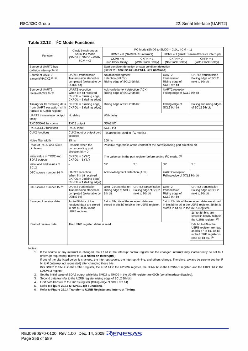
R8C/33C Group 22. Serial Interface (UART2)
REJ09B0570-0100 Rev.1.00 Dec. 14, 2009Page 356 of 589
Notes:1. If the source of any interrupt is changed, the IR bit in the interrupt control register for the changed interrupt may inadvertently be set to 1
(interrupt requested). (Refer to 11.8 Notes on Interrupts.) If one of the bits listed below is changed, the interrupt source, the interrupt timing, and others change. Therefore, always be sure to set the IRbit to 0 (interrupt not requested) after changing these bits.Bits SMD2 to SMD0 in the U2MR register, the IICM bit in the U2SMR register, the IICM2 bit in the U2SMR2 register, and the CKPH bit in theU2SMR3 register.
2. Set the initial value of SDA2 output while bits SMD2 to SMD0 in the U2MR register are 000b (serial interface disabled).3. Second data transfer to the U2RB register (rising edge of SCL2 9th bit)4. First data transfer to the U2RB register (falling edge of SCL2 9th bit)5. Refer to Figure 22.16 STSPSEL Bit Functions.6. Refer to Figure 22.14 Transfer to U2RB Register and Interrupt Timing.
Table 22.12 I2C Mode Functions
Function
Clock Synchronous Serial I/O Mode
(SMD2 to SMD0 = 001b, IICM = 0)
I2C Mode (SMD2 to SMD0 = 010b, IICM = 1)IICM2 = 0 (NACK/ACK interrupt) IICM2 = 1 (UART transmit/receive interrupt)CKPH = 0
(No Clock Delay) CKPH = 1
(With Clock Delay)CKPH = 0
(No Clock Delay)CKPH = 1
(With Clock Delay)Source of UART2 bus collision interrupt (1, 5)
− Start condition detection or stop condition detection(Refer to Table 22.13 STSPSEL Bit Functions)
Source of UART2 transmit/NACK2 (1, 6)
UART2 transmissionTransmission started orcompleted (selectable by U2IRS bit)
No acknowledgmentdetection (NACK)Rising edge of SCL2 9th bit
UART2 transmission Rising edge of SCL2 9th bit
UART2 transmission Falling edge of SCL2 next to 9th bit
Source of UART2 receive/ACK2 (1, 6)
UART2 receptionWhen 8th bit receivedCKPOL = 0 (rising edge)CKPOL = 1 (falling edge)
Acknowledgment detection (ACK)Rising edge of SCL2 9th bit
UART2 reception Falling edge of SCL2 9th bit
Timing for transferring datafrom UART reception shiftregister to U2RB register
CKPOL = 0 (rising edge)CKPOL = 1 (falling edge)
Rising edge of SCL2 9th bit Falling edge of SCL2 9th bit
Falling and rising edges of SCL2 9th bit
UART2 transmission output delay
No delay With delay
TXD2/SDA2 functions TXD2 output SDA2 I/ORXD2/SCL2 functions RXD2 input SCL2 I/OCLK2 functions CLK2 input or output port
selected− (Cannot be used in I2C mode.)
Noise filter width 15 ns 200 nsRead of RXD2 and SCL2 pin levels
Possible when the corresponding port direction bit = 0
Possible regardless of the content of the corresponding port direction bit.
Initial value of TXD2 and SDA2 outputs
CKPOL = 0 (“H”)CKPOL = 1 (“L”)
The value set in the port register before setting I2C mode. (2)
Initial and end values of SCL2
− “H” “L” “H” “L”
DTC source number 14 (6) UART2 receptionWhen 8th bit receivedCKPOL = 0 (rising edge)CKPOL = 1 (falling edge)
Acknowledgment detection (ACK) UART2 reception Falling edge of SCL2 9th bit
DTC source number 15 (6) UART2 transmissionTransmission started orcompleted (selectable by U2IRS bit)
UART2 transmission Rising edge of SCL2 9th bit
UART2 transmission Falling edge of SCL2 next to 9th bit
UART2 transmission Rising edge of SCL2 9th bit
UART2 transmission Falling edge of SCL2 next to 9th bit
Storage of receive data 1st to 8th bits of the received data are stored in bits b0 to b7 in the U2RB register.
1st to 8th bits of the received data are stored in bits b7 to b0 in the U2RB register.
1st to 7th bits of the received data are stored in bits b6 to b0 in the U2RB register. 8th bit is stored in bit b8 in the U2RB register.
1st to 8th bits are stored in bits b7 to b0 in the U2RB register. (3)
Read of receive data The U2RB register status is read. Bits b6 to b0 in the U2RB register are read as bits b7 to b1. Bit b8 in the U2RB register is read as bit b0. (4)

R8C/33C Group 22. Serial Interface (UART2)
REJ09B0570-0100 Rev.1.00 Dec. 14, 2009Page 357 of 589
Figure 22.14 Transfer to U2RB Register and Interrupt Timing
(1) IICM2 = 0 (ACK and NACK interrupts), CKPH = 0 (no clock delay)
D6 D5 D4 D3 D2 D1 D8 (ACK, NACK)D7SDA2
SCL2
D0
ACK interrupt (DTC source number 14 request),NACK interrupt
Transfer to U2RB registerb15
...b9 b8 b7 b0
U2RB register contentsD8 D7 D6 D5 D4 D3 D2 D1 D0
(2) IICM2 = 0, CKPH = 1 (with clock delay)
D6 D5 D4 D3 D2 D1D7SDA2
SCL2
D0
ACK interrupt (DTC source number 14 request),NACK interrupt
Transfer to U2RB registerb15
...b9 b8 b7 b0
D8 D7 D6 D5 D4 D3 D2 D1 D0
U2RB register contents
D8 (ACK, NACK)
(3) IICM2 = 1 (UART transmit/receive interrupt), CKPH = 0
D6 D5 D4 D3 D2 D1D7SDA2
SCL2
D0
Receive interrupt (DTC source number 14 request)
Transmitinterrupt
Transfer to U2RB registerb15
...b9 b8 b7 b0
D0 D7 D6 D5 D4 D3 D2 D1
U2RB register contents
D8 (ACK, NACK)
(4) IICM2 = 1, CKPH = 1
D6 D5 D4 D3 D2 D1D7SDA2
SCL2
D0
Transmit interrupt
Transfer to U2RB register
The above applies when:• CKDIR bit in U2MR register = 0 (master selected)
Receive interrupt(DTC source number 14 request)
b15
...b9 b8 b7 b0
D0 D7 D6 D5 D4 D3 D2 D1
U2RB register contents
Transfer to U2RB registerb15
...b9 b8 b7 b0
D8 D7 D6 D5 D4 D3 D2 D1 D0
U2RB register contents
D8 (ACK, NACK)
1st bit 2nd bit 3rd bit 4th bit 5th bit 6th bit 7th bit 8th bit 9th bit
1st bit 2nd bit 3rd bit 4th bit 5th bit 6th bit 7th bit 8th bit 9th bit
1st bit 2nd bit 3rd bit 4th bit 5th bit 6th bit 7th bit 8th bit 9th bit
1st bit 2nd bit 3rd bit 4th bit 5th bit 6th bit 7th bit 8th bit 9th bit

R8C/33C Group 22. Serial Interface (UART2)
REJ09B0570-0100 Rev.1.00 Dec. 14, 2009Page 358 of 589
22.5.1 Detection of Start and Stop ConditionsWhether a start or a stop condition has been detected is determined.A start condition detect interrupt request is generated when the SDA2 pin changes state from high to low whilethe SCL2 pin is in the high state. A stop condition detect interrupt request is generated when the SDA2 pinchanges state from low to high while the SCL2 pin is in the high state.Because the start and stop condition detect interrupts share an interrupt control register and vector, check theBBS bit in the U2SMR register to determine which interrupt source is requesting the interrupt. Figure 22.15 shows the Detection of Start and Stop Conditions.
Figure 22.15 Detection of Start and Stop Conditions
Setting upduration
Holdingduration
SCL2
SDA2(Start condition)
SDA2(Stop condition)
5 cycles of f1 < Setting up duration5 cycles of f1 < Holding duration

R8C/33C Group 22. Serial Interface (UART2)
REJ09B0570-0100 Rev.1.00 Dec. 14, 2009Page 359 of 589
22.5.2 Output of Start and Stop ConditionsA start condition is generated by setting the STAREQ bit in the U2SMR4 register to 1 (start).A restart condition is generated by setting the RSTAREQ bit in the U2SMR4 register to 1 (start).A stop condition is generated by setting the STPREQ bit in the U2SMR4 register to 1 (start).The output procedure is as follows:(1) Set the STAREQ bit, RSTAREQ bit or STPREQ bit to 1 (start).(2) Set the STSPSEL bit in the U2SMR4 register to 1 (output).Table 22.13 lists the STSPSEL Bit Functions. Figure 22.16 shows the STSPSEL Bit Functions.
Figure 22.16 STSPSEL Bit Functions
Table 22.13 STSPSEL Bit FunctionsFunction STSPSEL = 0 STSPSEL = 1
Output of pins SCL2 and SDA2
Output of transfer clock and data Output of start/stop conditions is accomplished by a program using ports (not automatically generated in hardware)
Output of start/stop conditions according to bits STAREQ, RSTAREQ, and STPREQ
Start/stop condition interrupt request generation timing
Detection of start/stop conditions Completion of start/stop condition generation
SDA2
Start conditiondetection interrupt
Stop conditiondetection interrupt
(1) Slave Mode CKDIR = 1 (external clock)
SCL2
SDA2
Start condition detectioninterrupt
Stop condition detectioninterrupt
(2) Master Mode CKDIR = 0 (internal clock), CKPH = 1 (with clock delay)
SCL2
Set STAREQ = 1(start) Set STPREQ = 1
(start)
STSPSEL bit 0
STSPSEL bit
Set to 1 bya program.
Set to 0 bya program.
Set to 1 bya program.
Set to 0 bya program.
1st 2nd 3rd 4th 5th 6th 7th 8th 9th bit
1st 2nd 3rd 4th 5th 6th 7th 8th 9th bit

R8C/33C Group 22. Serial Interface (UART2)
REJ09B0570-0100 Rev.1.00 Dec. 14, 2009Page 360 of 589
22.5.3 Transfer ClockThe transfer clock is used to transmit and receive data as is shown in Figure 22.14 Transfer to U2RB Registerand Interrupt Timing.The CSC bit in the U2SMR2 register is used to synchronize an internally generated clock (internal SCL2) andan external clock supplied to the SCL2 pin. When the CSC bit is set to 1 (clock synchronization enabled), if afalling edge on the SCL2 pin is detected while the internal SCL2 is high, the internal SCL2 goes low. The valuein the U2BRG register is reloaded and counting of the low-level intervals starts. If the internal SCL2 changesstate from low to high while the SCL2 pin is low, counting stops. If the SCL2 pin goes high, counting restarts.In this way, the UART2 transfer clock is equivalent to AND of the internal SCL2 and the clock signal applied tothe SCL2 pin. The transfer clock works from a half cycle before the falling edge of the internal SCL2 1st bit tothe rising edge of the 9th bit. To use this function, select an internal clock for the transfer clock.The SWC bit in the U2SMR2 register determines whether the SCL2 pin is fixed low or freed from low-leveloutput at the falling edge of the 9th clock pulse.If the SCLHI bit in the U2SMR4 register is set to 1 (enabled), SCL2 output is turned off (placed in the high-impedance state) when a stop condition is detected.Setting the SWC2 bit in the U2SMR2 register to 1 (“L” output) makes it possible to forcibly output a low-levelsignal from the SCL2 pin even while sending or receiving data. Setting the SWC2 bit to 0 (transfer clock)allows the transfer clock to be output from or supplied to the SCL2 pin, instead of outputting a low-level signal.If the SWC9 bit in the U2SMR4 register is set to 1 (SCL “L” hold enabled) when the CKPH bit in the U2SMR3register is 1, the SCL2 pin is fixed low at the falling edge of the clock pulse next to the 9th. Setting the SWC9bit to 0 (SCL “L” hold disabled) frees the SCL2 pin from low-level output.
22.5.4 SDA OutputThe data written to bits b7 to b0 (D7 to D0) in the U2TB register is output in descending order from D7.The 9th bit (D8) is ACK or NACK.Set the initial value of SDA2 transmit output when IICM is set to 1 (I2C mode) and bits SMD2 to SMD0 in theU2MR register are set to 000b (serial interface disabled).Bits DL2 to DL0 in the U2SMR3 register allow addition of no delays or a delay of 2 to 8 U2BRG count sourceclock cycles to the SDA2 output.Setting the SDHI bit in the U2SMR2 register to 1 (SDA output disabled) forcibly places the SDA2 pin in thehigh-impedance state. Do not write to the SDHI bit at the rising edge of the UART2 transfer clock.

R8C/33C Group 22. Serial Interface (UART2)
REJ09B0570-0100 Rev.1.00 Dec. 14, 2009Page 361 of 589
22.5.5 SDA InputWhen the IICM2 bit is set to 0, the 1st to 8th bits (D7 to D0) of received data are stored in bits b7 to b0 in theU2RB register. The 9th bit (D8) is ACK or NACK.When the IICM2 bit is set to 1, the 1st to 7th bits (D7 to D1) of received data are stored in bits b6 to b0 in theU2RB register and the 8th bit (D0) is stored in bit b8 in the U2RB register. Even when the IICM2 bit is set to 1,if the CKPH bit is 1, the same data as when the IICM2 bit is 0 can be read by reading the U2RB register afterthe rising edge of 9th bit of the clock.
22.5.6 ACK and NACK If the STSPSEL bit in the U2SMR4 register is set to 0 (start and stop conditions not output) and the ACKC bitin the U2SMR4 register is set to 1 (ACK data output), the value of the ACKD bit in the U2SMR4 register isoutput from the SDA2 pin.If the IICM2 bit is set to 0, a NACK interrupt request is generated if the SDA2 pin remains high at the risingedge of the 9th bit of transmit clock pulse. An ACK interrupt request is generated if the SDA2 pin is low at therising edge of the 9th bit of the transmit clock.If ACK2 (UART2 reception) is selected to generate a DTC request source, a DTC transfer can be activated bydetection of an acknowledge.
22.5.7 Initialization of Transmission/ReceptionIf a start condition is detected while the STAC bit is set to 1 (UART2 initialization enabled), the serial interfaceoperates as described below.• The transmit shift register is initialized, and the contents of the U2TB register are transferred to the transmit
shift register. In this way, the serial interface starts sending data when the next clock pulse is applied.However, the UART2 output value does not change state and remains the same as when a start condition wasdetected until the first bit of data is output in synchronization with the input clock.
• The receive shift register is initialized, and the serial interface starts receiving data when the next clock pulseis applied.
• The SWC bit is set to 1 (SCL wait output enabled). Consequently, the SCL2 pin is pulled low at the fallingedge of the 9th clock pulse.
Note that when UART2 transmission/reception is started using this function, the TI bit does not change state.Select the external clock as the transfer clock to start UART2 transmission/reception with this setting.
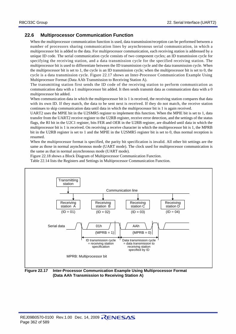
R8C/33C Group 22. Serial Interface (UART2)
REJ09B0570-0100 Rev.1.00 Dec. 14, 2009Page 362 of 589
22.6 Multiprocessor Communication FunctionWhen the multiprocessor communication function is used, data transmission/reception can be performed between anumber of processors sharing communication lines by asynchronous serial communication, in which amultiprocessor bit is added to the data. For multiprocessor communication, each receiving station is addressed by aunique ID code. The serial communication cycle consists of two component cycles; an ID transmission cycle forspecifying the receiving station, and a data transmission cycle for the specified receiving station. Themultiprocessor bit is used to differentiate between the ID transmission cycle and the data transmission cycle. Whenthe multiprocessor bit is set to 1, the cycle is an ID transmission cycle; when the multiprocessor bit is set to 0, thecycle is a data transmission cycle. Figure 22.17 shows an Inter-Processor Communication Example UsingMultiprocessor Format (Data AAh Transmission to Receiving Station A).The transmitting station first sends the ID code of the receiving station to perform communication ascommunication data with a 1 multiprocessor bit added. It then sends transmit data as communication data with a 0multiprocessor bit added.When communication data in which the multiprocessor bit is 1 is received, the receiving station compares that datawith its own ID. If they match, the data to be sent next is received. If they do not match, the receive stationcontinues to skip communication data until data in which the multiprocessor bit is 1 is again received.UART2 uses the MPIE bit in the U2SMR5 register to implement this function. When the MPIE bit is set to 1, datatransfer from the UART2 receive register to the U2RB register, receive error detection, and the settings of the statusflags, the RI bit in the U2C1 register, bits FER and OER in the U2RB register, are disabled until data in which themultiprocessor bit is 1 is received. On receiving a receive character in which the multiprocessor bit is 1, the MPRBbit in the U2RB register is set to 1 and the MPIE in the U2SMR5 register bit is set to 0, thus normal reception isresumed. When the multiprocessor format is specified, the parity bit specification is invalid. All other bit settings are thesame as those in normal asynchronous mode (UART mode). The clock used for multiprocessor communication isthe same as that in normal asynchronous mode (UART mode). Figure 22.18 shows a Block Diagram of Multiprocessor Communication Function.Table 22.14 lists the Registers and Settings in Multiprocessor Communication Function.
Figure 22.17 Inter-Processor Communication Example Using Multiprocessor Format (Data AAh Transmission to Receiving Station A)
01hSerial data AAh
(MPRB = 1) (MPRB = 0)
ID transmission cycle= receiving station
specification
Data transmission cycle= data transmission to
receiving stationspecified by ID
MPRB: Multiprocessor bit
(ID = 01) (ID = 02) (ID = 03) (ID = 04)
Receivingstation A
Receivingstation B
Receivingstation C
Receivingstation D
Transmittingstation
Communication line

R8C/33C Group 22. Serial Interface (UART2)
REJ09B0570-0100 Rev.1.00 Dec. 14, 2009Page 363 of 589
Figure 22.18 Block Diagram of Multiprocessor Communication Function
RXD2
1SP
2SPSP
SP PAR
PRYE = 0PARdisabled
PARenabledPRYE = 1
Clocksynchronoustype
UART
UART (7 bits)UART (8 bits)
UART(9 bits)
UART(7 bits)
UART (8 bits)UART (9 bits)
D7 D6 D5 D4 D3 D2 D1 D0
UART2 receive register
U2RBregister0 0 0 0 0 0 0 MPRB
Data bus high-order bits
Data bus low-order bits
D7 D6 D5 D4 D3 D2 D1 D0 U2TBregisterMPTB
TXD2
1SP
2SP
SP SP PARPARdisabledPRYE = 0
PARenabledPRYE = 1
Clocksynchronoustype
UART
UART (7 bits)UART (8 bits)
UART(9 bits)
UART(7 bits)
UART2 transmit register
0
SP: Stop bitPAR: Parity bitPRYE: Bit in U2MR registerDF2EN: Bit in URXDF registerMP: Bit in U2SMR5 register
DF2EN = 0
DF2EN = 1
Digitalfilter
Reception
Transmission
(5)
(2)
(1)
[Multiprocessor mode reception when MP = 1 (multiprocessor communication enabled)](1) Clock asynchronous (7 bits): Received D7 is transferred to b8 in the U2RB register.(2) Clock asynchronous (8 bits): Received D8 is transferred to b8 in the U2RB register.
[Multiprocessor mode transmission when MP = 1 (multiprocessor communication enabled)](3) Clock asynchronous (7 bits): b8 in the U2TB register is transferred externally as transfer data D7.(4) Clock asynchronous (8 bits): b8 in the U2TB register is transferred externally as transfer data D8.
[Multiprocessor mode transmission/reception](5) PAR is disabled.
(3)(4)
(5)
Clocksynchronous type
MSB/LSB conversion circuit
MSB/LSB conversion circuit
Clocksynchronoustype
Clocksynchronous type
UART (8 bits)UART (9 bits)
Clocksynchronoustype

R8C/33C Group 22. Serial Interface (UART2)
REJ09B0570-0100 Rev.1.00 Dec. 14, 2009Page 364 of 589
Notes:1. Set the MPTB bit to 1 when the ID data frame is transmitted. Set this bit to 0 when the data frame is
transmitted.2. If the MPRB bit is set to 1, received D7 to D0 are ID fields. If the MPRB bit is set to 0, received D7 to
D0 are data fields.
Table 22.14 Registers and Settings in Multiprocessor Communication FunctionRegister Bit Function
U2TB (1) b0 to b7 Set transmit data.MPTB Set to 0 or 1.
U2RB (2) b0 to b7 Receive data can be read. MPRB Multiprocessor bitOER, FER, SUM Error flag
U2BRG b0 to b7 Set the transfer rate.U2MR SMD2 to SMD0 Set to 100b when transfer data is 7 bits long.
Set to 101b when transfer data is 8 bits long.CKDIR Select the internal clock or external clock. STPS Select the stop bit.PRY, PRYE Parity detection function disabledIOPOL Set to 0.
U2C0 CLK0, CLK1 Select the U2BRG count source.CRS CTS or RTS function disabledTXEPT Transmit register empty flagCRD Set to 0.NCH Select TXD2 pin output mode.CKPOL Set to 0.UFORM Set to 0.
U2C1 TE Set to 1 to enable transmission.TI Transmit buffer empty flagRE Set to 1 to enable reception.RI Receive complete flagU2IRS Select the UART2 transmit interrupt source.U2LCH Set to 0.U2ERE Set to 0.
U2SMR b0 to b7 Set to 0.U2SMR2 b0 to b7 Set to 0.U2SMR3 b0 to b7 Set to 0.U2SMR4 b0 to b7 Set to 0.U2SMR5 MP Set to 1.
MPIE Set to 1.URXDF DF2EN Select the digital filter enabled or disabled.

R8C/33C Group 22. Serial Interface (UART2)
REJ09B0570-0100 Rev.1.00 Dec. 14, 2009Page 365 of 589
22.6.1 Multiprocessor TransmissionFigure 22.19 shows a Sample Flowchart of Multiprocessor Data Transmission. Set the MPBT bit in the U2TBregister to 1 for ID transmission cycles. Set the MPBT bit in the U2TB register to 0 for data transmission cycles.Other operations are the same as in universal asynchronous receiver/transmitter mode (UART mode).
Figure 22.19 Sample Flowchart of Multiprocessor Data Transmission
(1) Read the U2C1 register to confirm that the TI bit is set to 1. Then set the MPBT bit in the U2TB register to 0 or 1 and write transmit data to the U2TB register. Writing data to the U2TB register sets the TI bit to 0 automatically.
(2) When transmission completes, the TXEPT bit is set to 1 automatically.
(3) To continue data transmission, read that the TI bit is 1 and write data to the U2TB register. Writing data to the U2TB register sets the TI bit to 0 automatically.
Yes
No
End
Read the TI bit in the U2C1 register(1)
Set the MPBT bit in the U2TB register
Write transmit data tothe U2TB register
Read the TXEPT bitin the U2C0 register
TXEPT = 1?
Set the TE bitin the U2C1 register to 0
Continuedata transmission?
YesYes
No
(2)
(3)
TI = 1?
Start
No

R8C/33C Group 22. Serial Interface (UART2)
REJ09B0570-0100 Rev.1.00 Dec. 14, 2009Page 366 of 589
22.6.2 Multiprocessor ReceptionFigure 22.20 shows a Sample Flowchart of Multiprocessor Data Reception. When the MPIE bit in the U2SMR5register is set to 1, communication data is ignored until data in which the multiprocessor bit is 1 is received.Communication data with a 1 multiprocessor bit added is transferred to the U2RB register as receive data. Atthis time, a reception complete interrupt request is generated. Other operations are the same as in universalasynchronous receiver/transmitter mode (UART mode). Figure 22.21 shows a Receive Operation Exampleduring Multiprocessor Communication (with 8-Bit Data/Multiprocessor Bit/One-Stop Bit).
Figure 22.20 Sample Flowchart of Multiprocessor Data Reception
(1) Set the MPIE bit in the U2SMR5 register to 1.
(2) When the MPRB bit is detected to be 1, theMPIE bit is set to 0 and a reception completeinterrupt request can be generated.Read the U2C1 register to confirm that the RIbit is set to 1. If the RI bit is 1, read data in thereceive shift register and compare the data withits own station ID. Reading data in the U2RBregister sets the RI bit to 0 automatically.
(3) When the data matches the own station ID, thenext data reception starts. When the data doesnot match the ID, set the MPIE bit to 1 and theMCU enters the idle state.
(4) Read the U2C1 register to confirm that the RIbit is set to 1. Then read data in the receiveshift register.
(5) To discontinue reception, set the RE bit in theU2C0 register to 0 to complete reception.
To continue reception, restart the procedurefrom step (1).
Yes
No
End
Set the MPIE bitin the U2SMR5 register to 1(1)
Read datain the receive shift register
Read the RI bit in the U2C1 register
Read receive datain the U2RB register
RI = 1?
Set the RE bitin the U2C1 register to 0
Continuedata reception?
Yes
No
(4)
(5)
Start
RI = 1?
Read the RI bit in the U2C1 register
Own station ID?
Yes
Yes
(2)
(3)No
No

R8C/33C Group 22. Serial Interface (UART2)
REJ09B0570-0100 Rev.1.00 Dec. 14, 2009Page 367 of 589
Figure 22.21 Receive Operation Example during Multiprocessor Communication (with 8-Bit Data/Multiprocessor Bit/One-Stop Bit)
D0 D101 D7 1 D0 D1 D7 0 11 0 1
Receivedata (ID1)
Serial data
MPRBStartbit
Stopbit
Receivedata (DATA1) MPRB
Marked state(Idle state)
1 frame1 frame
1MP bit inU2SMR5 register
MPIE bit inU2SMR5 register
RI bit inU2C1 register
U2RB register
MCU operation
User processing
Detect the MPRB bit andset the MPIE bit to 0.
A reception completeinterrupt request isgenerated.
Set the RI bit to 0.
Read data in theU2RB register.
If data does not matchown station ID, set theMPIE bit to 1 again.
No reception completeinterrupt request isgenerated.The U2RB register retainsstate.
ID1
(a) When Data Does Not Match Own Station ID
D0 D101 D7 1 D0 D1 D7 0 11 0 1
Receivedata (ID2)
Serial data
MPRBStartbit
Stopbit
Receivedata (DATA2) MPRB
Marked state(Idle state)
1 frame1 frame
1MP bit inU2SMR5 register
MPIE bit inU2SMR5 register
RI bit inU2C1 register
U2RB register
MCU operation
User processing
Detect the MPRB bit andset the MPIE bit to 0.
A receptioncompleteinterrupt requestis generated.
Set the RI bit to 0.
Read data in theU2RB register.
If data matches ownstation ID, continuereception without anysetting changes.
Set the MPIE bitto 1 again.
ID2
(b) When Data Matches Own Station ID
DATA2ID1
A receptioncompleteinterrupt requestis generated.
Set the RI bit to 0.
Read data in theU2RB register.
MPRB: Bit in U2RB registerMPIE: Bit in U2SMR5 register

R8C/33C Group 22. Serial Interface (UART2)
REJ09B0570-0100 Rev.1.00 Dec. 14, 2009Page 368 of 589
22.6.3 RXD2 Digital Filter Select FunctionWhen the DF2EN bit in the URXDF register is set to 1 (RXD2 digital filer enabled), the RXD2 input signal isloaded internally via the digital filter circuit for noise reduction. The noise canceller consists of three cascadedlatch circuits and a match detection circuit. The RXD2 input signal is sampled on the internal basic clock with afrequency 16 times the bit rate. It is recognized as a signal and the level is passed forward to the next circuitwhen three latch outputs match. When the outputs do not match, the previous value is retained. In other words, when the level is changed within three clocks, the change is recognized as not a signal but noise.Figure 22.22 shows a Block Diagram of RXD2 Digital Filter Circuit.
Figure 22.22 Block Diagram of RXD2 Digital Filter Circuit
C
D Q
Latch
C
D Q
Latch
Matchdetection
circuit
RXD2input signal
Samplingclock
Sampling clock
URXDFregister
(DF2EN bit)
C
D Q
Latch
Internal RXD2input signal
Internal basic clockperiod (1)
Note:1. When the CKDIR bit in the U2MR register is 0 (internal clock), the internal basic clock is set to fj/(n+1)
(fj = f1, f8, f32, fC; n = setting value in the U2BRG register).When the CKDIR bit in the U2MR register is 1 (external clock), the internal basic clock is set to fEXT/(n+1)(fEXT is input from the CLK2 pin. n = setting value in the U2BRG register).

R8C/33C Group 22. Serial Interface (UART2)
REJ09B0570-0100 Rev.1.00 Dec. 14, 2009Page 369 of 589
22.7 Notes on Serial Interface (UART2)
22.7.1 Clock Synchronous Serial I/O Mode
22.7.1.1 Transmission/ReceptionWhen the RTS function is used with an external clock, the RTS2 pin outputs “L,” which informs thetransmitting side that the MCU is ready for a receive operation. The RTS2 pin outputs “H” when a receiveoperation starts. Therefore, the transmit timing and receive timing can be synchronized by connecting the RTS2pin to the CTS2 pin of the transmitting side. The RTS function is disabled when an internal clock is selected.
22.7.1.2 TransmissionIf an external clock is selected, the following conditions must be met while the external clock is held high whenthe CKPOL bit in the U2C0 register is set to 0 (transmit data output at the falling edge and receive data input atthe rising edge of the transfer clock), or while the external clock is held low when the CKPOL bit is set to 1(transmit data output at the rising edge and receive data input at the falling edge of the transfer clock).• The TE bit in the U2C1 register = 1 (transmission enabled)• The TI bit in the U2C1 register = 0 (data present in the U2TB register)• If the CTS function is selected, input on the CTS2 pin = “L”
22.7.1.3 ReceptionIn clock synchronous serial I/O mode, the shift clock is generated by activating the transmitter. Set the UART2-associated registers for transmit operation even if the MCU is used for receive operation only. Dummy data isoutput from the TXD2 pin while receiving.
When an internal clock is selected, the shift clock is generated by setting the TE bit in the U2C1 register to 1(transmission enabled) and placing dummy data in the U2TB register. When an external clock is selected, setthe TE bit to 1 (transmission enabled), place dummy data in the U2TB register, and input an external clock tothe CLK2 pin to generate the shift clock.
If data is received consecutively, an overrun error occurs when the RE bit in the U2C1 register is set to 1 (datapresent in the U2RB register) and the next receive data is received in the UART2 receive register. Then, theOER bit in the U2RB register is set to 1 (overrun error). At this time, the U2RB register value is undefined. If anoverrun error occurs, the IR bit in the S2RIC register remains unchanged.
To receive data consecutively, set dummy data in the low-order byte in the U2TB register per each receiveoperation.
If an external clock is selected, the following conditions must be met while the external clock is held high whenthe CKPOL bit is set to 0, or while the external clock is held low when the CKPOL bit is set to 1.• The RE bit in the U2C1 register = 1 (reception enabled)• The TE bit in the U2C1 register = 1 (transmission enabled)• The TI bit in the U2C1 register = 0 (data present in the U2TB register)

R8C/33C Group 22. Serial Interface (UART2)
REJ09B0570-0100 Rev.1.00 Dec. 14, 2009Page 370 of 589
22.7.2 Special Mode 1 (I2C Mode)When generating start, stop, and restart conditions, set the STSPSEL bit in the U2SMR4 register to 0 and waitfor more than half cycle of the transfer clock before changing each condition generation bit (STAREQ,RSTAREQ, and STPREQ) from 0 to 1.

R8C/33C Group 23. Clock Synchronous Serial Interface
REJ09B0570-0100 Rev.1.00 Dec. 14, 2009Page 371 of 589
23. Clock Synchronous Serial InterfaceThe clock synchronous serial interface is configured as follows.
Clock synchronous serial interface
The clock synchronous serial interface uses the registers at addresses 0193h to 019Dh. Registers, bits, symbols, andfunctions vary even for the same addresses depending on the mode. Refer to the registers of each function for details.Also, the differences between clock synchronous communication mode and clock synchronous serial mode are theoptions of the transfer clock, clock output format, and data output format.
23.1 Mode SelectionThe clock synchronous serial interface has four modes.Table 23.1 lists the Mode Selections. Refer to 24. Synchronous Serial Communication Unit (SSU), 25. I2C busInterface and the sections that follow for details of each mode.
Synchronous serial communication unit (SSU) Clock synchronous communication mode
4-wire bus communication mode
I2C bus Interface I2C bus interface mode
Clock synchronous serial mode
Table 23.1 Mode Selections
IICSEL Bit in SSUIICSR Register
Bit 7 in 0198h(ICE Bit in ICCR1
Register)
Bit 0 in 019Dh(SSUMS Bit in SSMR2
Register, FS Bit in SAR Register)
Function Mode
0 0 0 Synchronous serial communication unit
Clock synchronous communication mode
0 0 1 4-wire bus communication mode1 1 0 I2C bus interface I2C bus interface mode1 1 1 Clock synchronous serial mode

R8C/33C Group 24. Synchronous Serial Communication Unit (SSU)
REJ09B0570-0100 Rev.1.00 Dec. 14, 2009Page 372 of 589
24. Synchronous Serial Communication Unit (SSU)Synchronous serial communication unit (SSU) supports clock synchronous serial data communication.
24.1 OverviewTable 24.1 lists the Synchronous Serial Communication Unit Specifications and Figure 24.1 shows a BlockDiagram of Synchronous Serial Communication Unit. Table 24.2 lists the Pin Configuration of Synchronous SerialCommunication Unit.
Note:1. Synchronous serial communication unit has only one interrupt vector table.
Table 24.1 Synchronous Serial Communication Unit SpecificationsItem Specification
Transfer data format • Transfer data length: 8 to 16 bitsContinuous transmission and reception of serial data are supported since both transmitter and receiver have buffer structures.
Operating modes • Clock synchronous communication mode• 4-wire bus communication mode (including bidirectional communication)
Master/slave device SelectableI/O pins SSCK (I/O): Clock I/O pin
SSI (I/O): Data I/O pinSSO (I/O): Data I/O pinSCS (I/O): Chip-select I/O pin
Transfer clocks • When the MSS bit in the SSCRH register is set to 0 (operates as slave device), external clock is selected (input from SSCK pin).
• When the MSS bit in the SSCRH register is set to 1 (operates as master device), internal clock (selectable among f1/256, f1/128, f1/64, f1/32, f1/16, f1/8 and f1/4, output from SSCK pin) is selected.
• Clock polarity and phase of SSCK can be selected.Receive error detection • Overrun error
Overrun error occurs during reception and completes in error. While the RDRF bit in the SSSR register is set to 1 (data in the SSRDR register) and when next serial data receive is completed, the ORER bit is set to 1.
Multimaster error detection
• Conflict errorWhen the SSUMS bit in the SSMR2 register is set to 1 (4-wire bus communication mode) and the MSS bit in the SSCRH register is set to 1 (operates as master device) and when starting a serial communication, the CE bit in the SSSR register is set to 1 if “L” applies to the SCS pin input. When the SSUMS bit in the SSMR2 register is set to 1 (4-wire bus communication mode), the MSS bit in the SSCRH register is set to 0 (operates as slave device) and the SCS pin input changes state from “L” to “H”, the CE bit in the SSSR register is set to 1.
Interrupt requests 5 interrupt requests (transmit-end, transmit-data-empty, receive-data-full, overrun error, and conflict error) (1).
Select functions • Data transfer directionSelects MSB-first or LSB-first
• SSCK clock polaritySelects “L” or “H” level when clock stops
• SSCK clock phaseSelects edge of data change and data download

R8C/33C Group 24. Synchronous Serial Communication Unit (SSU)
REJ09B0570-0100 Rev.1.00 Dec. 14, 2009Page 373 of 589
Figure 24.1 Block Diagram of Synchronous Serial Communication Unit
Table 24.2 Pin Configuration of Synchronous Serial Communication Unit
Pin Name Assigned Pin I/O Function
SSI P3_3, P3_4, or P1_6 I/O Data I/O pin
SCS P3_3 or P3_4 I/O Chip-select signal I/O pin
SSCK P3_5 I/O Clock I/O pin
SSO P3_7 I/O Data I/O pin
SSMR register
Dat
a bu
s
Transmit/receivecontrol circuit
SSCRL register
SSCRH register
SSER register
SSSR register
SSMR2 register
SSTDR register
SSTRSR register
SSRDR register
Selector
Multiplexer
SSO
SSI
SCS
SSCK
Interrupt requests(TXI, TEI, RXI, OEI, and CEI)
Internal clockgeneration
circuit
f1
Internal clock (f1/i)
i = 4, 8, 16, 32, 64, 128, or 256

R8C/33C Group 24. Synchronous Serial Communication Unit (SSU)
REJ09B0570-0100 Rev.1.00 Dec. 14, 2009Page 374 of 589
24.2 Registers
24.2.1 Module Standby Control Register (MSTCR)
Notes:1. When the MSTIIC bit is set to 1 (standby), any access to the SSU or the I2C bus associated registers (addresses
0193h to 019Dh) is disabled.2. When the MSTTRC bit is set to 1 (standby), any access to the timer RC associated registers (addresses 0120h
to 0133h) is disabled.
Address 0008hBit b7 b6 b5 b4 b3 b2 b1 b0
Symbol — — MSTTRC MSTTRD MSTIIC — — —After Reset 0 0 0 0 0 0 0 0
Bit Symbol Bit Name Function R/Wb0 — Nothing is assigned. If necessary, set to 0. When read, the content is 0. —b1 —b2 —b3 MSTIIC SSU, I2C bus standby bit 0: Active
1: Standby (1)R/W
b4 MSTTRD Power consumption reduce bit Set to 1. The power consumption can be reduced.
R/W
b5 MSTTRC Timer RC standby bit 0: Active1: Standby (2)
R/W
b6 — Nothing is assigned. If necessary, set to 0. When read, the content is 0. —b7 —

R8C/33C Group 24. Synchronous Serial Communication Unit (SSU)
REJ09B0570-0100 Rev.1.00 Dec. 14, 2009Page 375 of 589
24.2.2 SSU/IIC Pin Select Register (SSUIICSR)
Address 018ChBit b7 b6 b5 b4 b3 b2 b1 b0
Symbol — — — — — — — IICSELAfter Reset 0 0 0 0 0 0 0 0
Bit Symbol Bit Name Function R/Wb0 IICSEL SSU/I2C bus switch bit 0: SSU function selected
1: I2C bus function selectedR/W
b1 — Reserved bit Set to 0. R/Wb2 — Nothing is assigned. If necessary, set to 0. When read, the content is 0. —b3 —b4 — Reserved bits Set to 0. R/Wb5 —b6 —b7 —

R8C/33C Group 24. Synchronous Serial Communication Unit (SSU)
REJ09B0570-0100 Rev.1.00 Dec. 14, 2009Page 376 of 589
24.2.3 SS Bit Counter Register (SSBR)
Note:1. Do not write to bits BS0 to BS3 during SSU operation.
To set the SSBR register, set the RE bit in the SSER register to 0 (reception disabled) and the TE bit to 0(transmission disabled).
Bits BS0 to BS3 (SSU Data Transfer Length Set Bit)As the SSU data transfer length, 8 to 16 bits can be used.
24.2.4 SS Transmit Data Register (SSTDR)
Note:1. When the SSU data transfer length is set to 9 bits or more with the SSBR register, access the SSTDR register in
16-bit units.
Address 0193hBit b7 b6 b5 b4 b3 b2 b1 b0
Symbol — — — — BS3 BS2 BS1 BS0After Reset 1 1 1 1 1 0 0 0
Bit Symbol Bit Name Function R/Wb0 BS0 SSU data transfer length set bit (1) b3 b2 b1 b0
0 0 0 0: 16 bits 1 0 0 0: 8 bits 1 0 0 1: 9 bits 1 0 1 0: 10 bits 1 0 1 1: 11 bits 1 1 0 0: 12 bits 1 1 0 1: 13 bits 1 1 1 0: 14 bits 1 1 1 1: 15 bits
R/Wb1 BS1 R/Wb2 BS2 R/Wb3 BS3 R/W
b4 — Nothing is assigned. If necessary, set to 0. When read, the content is 1. —b5 —b6 —b7 —
Address 0195h to 0194hBit b7 b6 b5 b4 b3 b2 b1 b0
Symbol — — — — — — — —After Reset 1 1 1 1 1 1 1 1
Bit b15 b14 b13 b12 b11 b10 b9 b8Symbol — — — — — — — —
After Reset 1 1 1 1 1 1 1 1
Bit Symbol Function R/Wb15 to b0 — Store the transmit data. (1)
The stored transmit data is transferred to the SSTRSR register and transmission is started when it is detected that the SSTRSR register is empty.When the next transmit data is written to the SSTDR register during the data transmission from the SSTRSR register, the data can be transmitted continuously.When the MLS bit in the SSMR register is set to 1 (transfer data with LSB-first), the data in which MSB and LSB are reversed is read, after writing to the SSTDR register.
R/W

R8C/33C Group 24. Synchronous Serial Communication Unit (SSU)
REJ09B0570-0100 Rev.1.00 Dec. 14, 2009Page 377 of 589
24.2.5 SS Receive Data Register (SSRDR)
Notes:1. The SSRDR register retains the data received before an overrun error occurs (ORER bit in the SSSR register set
to 1 (overrun error)). When an overrun error occurs, the receive data may contain errors and therefore should bediscarded.
2. When the SSU data transfer length is set to 9 bits or more with the SSBR register, access the SSRDR register in16-bit units.
24.2.6 SS Control Register H (SSCRH)
Notes:1. The set clock is used when the MSS bit is set to 1 (operates as master device).2. The SSCK pin functions as the transfer clock output pin when the MSS bit is set to 1 (operates as master
device). The MSS bit is set to 0 (operates as slave device) when the CE bit in the SSSR register is set to 1(conflict error occurs).
3. The RSSTP bit is disabled when the MSS bit is set to 0 (operates as slave device).
Address 0197h to 0196hBit b7 b6 b5 b4 b3 b2 b1 b0
Symbol — — — — — — — —After Reset 1 1 1 1 1 1 1 1
Bit b15 b14 b13 b12 b11 b10 b9 b8Symbol — — — — — — — —
After Reset 1 1 1 1 1 1 1 1
Bit Symbol Function R/Wb15 to b0 — Store the receive data. (1, 2)
The receive data is transferred to the SSRDR register and the receive operation is completed when 1 byte of data has been received by the SSTRSR register. At this time, the next receive operation is possible.Continuous reception is possible using registers SSTRSR and SSRDR.
R
Address 0198hBit b7 b6 b5 b4 b3 b2 b1 b0
Symbol — RSSTP MSS — — CKS2 CKS1 CKS0After Reset 0 0 0 0 0 0 0 0
Bit Symbol Bit Name Function R/Wb0 CKS0 Transfer clock select bit (1) b2 b1 b0
0 0 0: f1/256 0 0 1: f1/128 0 1 0: f1/64 0 1 1: f1/32 1 0 0: f1/16 1 0 1: f1/8 1 1 0: f1/4 1 1 1: Do not set.
R/Wb1 CKS1 R/Wb2 CKS2 R/W
b3 — Nothing is assigned. If necessary, set to 0. When read, the content is 0. —b4 —b5 MSS Master/slave device select bit (2) 0: Operates as slave device
1: Operates as master deviceR/W
b6 RSSTP Receive single stop bit (3) 0: Maintains receive operation after receiving 1 byte of data
1: Completes receive operation after receiving 1 byte of data
R/W
b7 — Nothing is assigned. If necessary, set to 0. When read, the content is 0. —

R8C/33C Group 24. Synchronous Serial Communication Unit (SSU)
REJ09B0570-0100 Rev.1.00 Dec. 14, 2009Page 378 of 589
24.2.7 SS Control Register L (SSCRL)
Notes:1. Registers SSBR, SSCRH, SSCRL, SSMR, SSER, SSSR, SSMR2, SSTDR, and SSRDR.2. For the data output after serial data transmission, the last bit value of the transmitted serial data is retained.
If the content of the SOL bit is rewritten before or after serial data transmission, the change is immediatelyreflected in the data output.When writing to the SOL bit, set the SOLP bit to 0 and the SOL bit to 0 or 1 simultaneously by the MOVinstruction.
3. Do not write to the SOL bit during data transfer.
Address 0199hBit b7 b6 b5 b4 b3 b2 b1 b0
Symbol — — SOL SOLP — — SRES —After Reset 0 1 1 1 1 1 0 1
Bit Symbol Bit Name Function R/Wb0 — Nothing is assigned. If necessary, set to 0. When read, the content is 1. —b1 SRES SSU control unit reset bit Writing 1 to this bit resets the SSU control unit and the
SSTRSR register.The value in the SSU internal register (1) is retained.
R/W
b2 — Nothing is assigned. If necessary, set to 0. When read, the content is 1. —b3 —b4 SOLP SOL write protect bit (2) The output level can be changed by the SOL bit when
this bit is set to 0.The SOLP bit remains unchanged even if 1 is written to it. When read, the content is 1.
R/W
b5 SOL Serial data output value setting bit When read0: The serial data output is set to “L”.1: The serial data output is set to “H”.When written (2, 3)
0: The data output is “L”.1: The data output is “H”.
R/W
b6 — Nothing is assigned. If necessary, set to 0. When read, the content is 1. —b7 — Nothing is assigned. If necessary, set to 0. When read, the content is 0. —

R8C/33C Group 24. Synchronous Serial Communication Unit (SSU)
REJ09B0570-0100 Rev.1.00 Dec. 14, 2009Page 379 of 589
24.2.8 SS Mode Register (SSMR)
Note:1. Refer to 24.3.1.1 Association between Transfer Clock Polarity, Phase, and Data for the settings of the CPHS
and CPOS bits.When the SSUMS bit in the SSMR2 register is set to 0 (clock synchronous communication mode), set the CPHSbit to 0 and the CPOS bit to 0.
Address 019AhBit b7 b6 b5 b4 b3 b2 b1 b0
Symbol MLS CPOS CPHS — BC3 BC2 BC1 BC0After Reset 0 0 0 1 0 0 0 0
Bit Symbol Bit Name Function R/Wb0 BC0 Bits counter 3 to 0 b3 b2 b1 b0
0 0 0 0: 16 bits left 0 0 0 1: 1 bit left 0 0 1 0: 2 bits left 0 0 1 1: 3 bits left 0 1 0 0: 4 bits left 0 1 0 1: 5 bits left 0 1 1 0: 6 bits left 0 1 1 1: 7 bits left 1 0 0 0: 8 bits left 1 0 0 1: 9 bits left 1 0 1 0: 10 bits left 1 0 1 1: 11 bits left 1 1 0 0: 12 bits left 1 1 0 1: 13 bits left 1 1 1 0: 14 bits left 1 1 1 1: 15 bits left
Rb1 BC1 Rb2 BC2 Rb3 BC3 R
b4 — Nothing is assigned. If necessary, set to 0. When read, the content is 1. —b5 CPHS SSCK clock phase select bit (1) 0: Change data at odd edge
(Download data at even edge)1: Change data at even edge
(Download data at odd edge)
R/W
b6 CPOS SSCK clock polarity select bit (1) 0: “H” when clock stops1: “L” when clock stops
R/W
b7 MLS MSB first/LSB first select bit 0: Transfers data MSB first1: Transfers data LSB first
R/W

R8C/33C Group 24. Synchronous Serial Communication Unit (SSU)
REJ09B0570-0100 Rev.1.00 Dec. 14, 2009Page 380 of 589
24.2.9 SS Enable Register (SSER)Address 019Bh
Bit b7 b6 b5 b4 b3 b2 b1 b0Symbol TIE TEIE RIE TE RE — — CEIE
After Reset 0 0 0 0 0 0 0 0
Bit Symbol Bit Name Function R/Wb0 CEIE Conflict error interrupt enable bit 0: Disables conflict error interrupt request
1: Enables conflict error interrupt requestR/W
b1 — Nothing is assigned. If necessary, set to 0. When read, the content is 0. —b2 —b3 RE Receive enable bit 0: Disables receive
1: Enables receiveR/W
b4 TE Transmit enable bit 0: Disables transmit1: Enables transmit
R/W
b5 RIE Receive interrupt enable bit 0: Disables receive data full and overrun error interrupt request
1: Enables receive data full and overrun error interrupt request
R/W
b6 TEIE Transmit end interrupt enable bit 0: Disables transmit end interrupt request1: Enables transmit end interrupt request
R/W
b7 TIE Transmit interrupt enable bit 0: Disables transmit data empty interrupt request1: Enables transmit data empty interrupt request
R/W

R8C/33C Group 24. Synchronous Serial Communication Unit (SSU)
REJ09B0570-0100 Rev.1.00 Dec. 14, 2009Page 381 of 589
24.2.10 SS Status Register (SSSR)
Notes:1. Writing 1 to CE, ORER, RDRF, TEND, or TDRE bits is invalid. To set any of these bits to 0, first read 1 then write
0.2. When the serial communication is started while the SSUMS bit in the SSMR2 register is set to 1 (four-wire bus
communication mode) and the MSS bit in the SSCRH register is set to 1 (operates as master device), the CE bitis set to 1 if “L” is applied to the SCS pin input. Refer to 24.5.4 SCS Pin Control and Arbitration for moreinformation.When the SSUMS bit in the SSMR2 register is set to 1 (four-wire bus communication mode), the MSS bit in theSSCRH register is set to 0 (operates as slave device) and the SCS pin input changes the level from “L” to “H”during transfer, the CE bit is set to 1.
3. Indicates when overrun errors occur and receive completes by error reception. If the next serial data receiveoperation is completed while the RDRF bit is set to 1 (data in the SSRDR register), the ORER bit is set to 1.After the ORER bit is set to 1 (overrun error), receive operation is disabled while the bit remains 1.
4. The RDRF bit is set to 0 when reading out the data from the SSRDR register.5. Bits TEND and TDRE are set to 0 when writing data to the SSTDR register.6. The TDRE bit is set to 1 when the TE bit in the SSER register is set to 1 (transmit enabled).
If the SSSR register is accessed continuously, insert one or more NOP instructions between the instructionsused for access.
Address 019ChBit b7 b6 b5 b4 b3 b2 b1 b0
Symbol TDRE TEND RDRF — — ORER — CEAfter Reset 0 0 0 0 0 0 0 0
Bit Symbol Bit Name Function R/Wb0 CE Conflict error flag (1) 0: No conflict errors generated
1: Conflict errors generated (2)R/W
b1 — Nothing is assigned. If necessary, set to 0. When read, the content is 0. —b2 ORER Overrun error flag (1) 0: No overrun errors generated
1: Overrun errors generated (3)R/W
b3 — Nothing is assigned. If necessary, set to 0. When read, the content is 0. —b4 —b5 RDRF Receive data register full flag (1, 4) 0: No data in SSRDR register
1: Data in SSRDR registerR/W
b6 TEND Transmit end flag (1, 5) 0: The TDRE bit is set to 0 when transmitting the last bit of transmit data
1: The TDRE bit is set to 1 when transmitting the last bit of transmit data
R/W
b7 TDRE Transmit data empty flag (1, 5, 6) 0: Data is not transferred from registers SSTDR to SSTRSR
1: Data is transferred from registers SSTDR to SSTRSR
R/W

R8C/33C Group 24. Synchronous Serial Communication Unit (SSU)
REJ09B0570-0100 Rev.1.00 Dec. 14, 2009Page 382 of 589
24.2.11 SS Mode Register 2 (SSMR2)
Notes:1. Refer to 24.3.2.1 Association between Data I/O Pins and SS Shift Register for information on combinations of
data I/O pins.2. The SCS pin functions as a port, regardless of the values of bits CSS0 and CSS1 when the SSUMS bit is set to
0 (clock synchronous communication mode).3. This bit functions as the SCS input pin before starting transfer.4. The BIDE bit is disabled when the SSUMS bit is set to 0 (clock synchronous communication mode).5. When the SOOS bit is set to 0 (CMOS output), set the port direction register bits corresponding to pins SSI and
SSO to 0 (input mode).
Address 019DhBit b7 b6 b5 b4 b3 b2 b1 b0
Symbol BIDE SCKS CSS1 CSS0 SCKOS SOOS CSOS SSUMSAfter Reset 0 0 0 0 0 0 0 0
Bit Symbol Bit Name Function R/Wb0 SSUMS SSU mode select bit (1) 0: Clock synchronous communication mode
1: Four-wire bus communication modeR/W
b1 CSOS SCS pin open drain output select bit
0: CMOS output1: N-channel open-drain output
R/W
b2 SOOS Serial data pin open output drain select bit (1)
0: CMOS output (5)
1: N-channel open-drain outputR/W
b3 SCKOS SSCK pin open drain output select bit
0: CMOS output1: N-channel open-drain output
R/W
b4 CSS0 SCS pin select bit (2) b5 b4 0 0: Functions as port 0 1: Functions as SCS input pin 1 0: Functions as SCS output pin (3)
1 1: Functions as SCS output pin (3)
R/Wb5 CSS1 R/W
b6 SCKS SSCK pin select bit 0: Functions as port1: Functions as serial clock pin
R/W
b7 BIDE Bidirectional mode enable bit (1, 4) 0: Standard mode (communication using 2 pins of data input and data output)
1: Bidirectional mode (communication using 1 pin of data input and data output)
R/W

R8C/33C Group 24. Synchronous Serial Communication Unit (SSU)
REJ09B0570-0100 Rev.1.00 Dec. 14, 2009Page 383 of 589
24.3 Common Items for Multiple Modes
24.3.1 Transfer ClockThe transfer clock can be selected from among seven internal clocks (f1/256, f1/128, f1/64, f1/32, f1/16, f1/8,and f1/4) and an external clock. When using synchronous serial communication unit, set the SCKS bit in the SSMR2 register to 1 and select theSSCK pin as the serial clock pin. When the MSS bit in the SSCRH register is set to 1 (operates as master device), an internal clock can beselected and the SSCK pin functions as output. When transfer is started, the SSCK pin outputs clocks of thetransfer rate selected by bits CKS0 to CKS2 in the SSCRH register. When the MSS bit in the SSCRH register is set to 0 (operates as slave device), an external clock can be selectedand the SSCK pin functions as input.
24.3.1.1 Association between Transfer Clock Polarity, Phase, and DataThe association between the transfer clock polarity, phase and data changes according to the combination of theSSUMS bit in the SSMR2 register and bits CPHS and CPOS in the SSMR register.Figure 24.2 shows the Association between Transfer Clock Polarity, Phase, and Transfer Data. Also, the MSB-first transfer or LSB-first transfer can be selected by setting the MLS bit in the SSMR register.When the MLS bit is set to 1, transfer is started from the LSB and proceeds to the MSB. When the MLS bit isset to 0, transfer is started from the MSB and proceeds to the LSB.

R8C/33C Group 24. Synchronous Serial Communication Unit (SSU)
REJ09B0570-0100 Rev.1.00 Dec. 14, 2009Page 384 of 589
Figure 24.2 Association between Transfer Clock Polarity, Phase, and Transfer Data
SSCK
b0SSO, SSI
• SSUMS = 0 (clock synchronous communication mode), CPHS bit = 0 (data change at oddedge), and CPOS bit = 0 (“H” when clock stops)
b1 b2 b3 b4 b5 b6 b7
SSCKCPOS = 0
(“H” when clock stops)
b0SSO, SSI
• SSUMS = 1 (4-wire bus communication mode) and CPHS = 0 (data change at odd edge)
b1 b2 b3 b4 b5 b6 b7
SSCKCPOS = 1
(“L” when clock stops)
SCS
SSCKCPOS = 0
(“H” when clock stops)
SSO, SSI
• SSUMS = 1 (4-wire bus communication mode) and CPHS = 1 (data download at odd edge)
SSCKCPOS = 1
(“L” when clock stops)
SCS
b0 b1 b2 b3 b4 b5 b6 b7
CPHS and CPOS: Bits in SSMR register, SSUMS: Bit in SSMR2 register

R8C/33C Group 24. Synchronous Serial Communication Unit (SSU)
REJ09B0570-0100 Rev.1.00 Dec. 14, 2009Page 385 of 589
24.3.2 SS Shift Register (SSTRSR)The SSTRSR register is a shift register for transmitting and receiving serial data. When transmit data is transferred from the SSTDR register to the SSTRSR register and the MLS bit in theSSMR register is set to 0 (MSB-first), the bit 0 in the SSTDR register is transferred to bit 0 in the SSTRSRregister. When the MLS bit is set to 1 (LSB-first), bit 7 in the SSTDR register is transferred to bit 0 in theSSTRSR register.
24.3.2.1 Association between Data I/O Pins and SS Shift RegisterThe connection between the data I/O pins and SSTRSR register (SS shift register) changes according to acombination of the MSS bit in the SSCRH register and the SSUMS bit in the SSMR2 register. The connectionalso changes according to the BIDE bit in the SSMR2 register.Figure 24.3 shows the Association between Data I/O Pins and SSTRSR Register.
Figure 24.3 Association between Data I/O Pins and SSTRSR Register
SSTRSR register SSO
SSI
• SSUMS = 0(clock synchronous communication mode)
SSTRSR register SSO
SSI
• SSUMS = 1 (4-wire bus communication mode),BIDE = 0 (standard mode), and MSS = 0 (operatesas slave device)
SSTRSR register SSO
SSI
• SSUMS = 1 (4-wire bus communication mode),BIDE = 0 (standard mode), and MSS = 1 (operates asmaster device)
SSTRSR register SSO
SSI
• SSUMS = 1 (4-wire bus communication mode) andBIDE = 1 (bidirectional mode)
R8C/33C Group 24. Synchronous Serial Communication Unit (SSU)
REJ09B0570-0100 Rev.1.00 Dec. 14, 2009Page 386 of 589
24.3.3 Interrupt RequestsSynchronous serial communication unit has five interrupt requests: transmit data empty, transmit end, receivedata full, overrun error, and conflict error. Since these interrupt requests are assigned to the synchronous serialcommunication unit interrupt vector table, determining interrupt sources by flags is required.Table 24.3 shows the Synchronous Serial Communication Unit Interrupt Requests.
CEIE, RIE, TEIE and TIE: Bits in SSER registerORER, RDRF, TEND and TDRE: Bits in SSSR register
If the generation conditions in Table 24.3 are met, a synchronous serial communication unit interrupt request isgenerated. Set each interrupt source to 0 by a synchronous serial communication unit interrupt routine.
However, the TDRE and TEND bits are automatically set to 0 by writing transmit data to the SSTDR register andthe RDRF bit is automatically set to 0 by reading the SSRDR register. In particular, the TDRE bit is set to 1 (datatransmitted from registers SSTDR to SSTRSR) at the same time transmit data is written to the SSTDR register.Setting the TDRE bit to 0 (data not transmitted from registers SSTDR to SSTRSR) can cause an additional byte ofdata to be transmitted.
Table 24.3 Synchronous Serial Communication Unit Interrupt RequestsInterrupt Request Abbreviation Generation Condition
Transmit data empty TXI TIE = 1, TDRE = 1Transmit end TEI TEIE = 1, TEND = 1Receive data full RXI RIE = 1, RDRF = 1Overrun error OEI RIE = 1, ORER = 1Conflict error CEI CEIE = 1, CE = 1

R8C/33C Group 24. Synchronous Serial Communication Unit (SSU)
REJ09B0570-0100 Rev.1.00 Dec. 14, 2009Page 387 of 589
24.3.4 Communication Modes and Pin FunctionsSynchronous serial communication unit switches the functions of the I/O pins in each communication modeaccording to the setting of the MSS bit in the SSCRH register and bits RE and TE in the SSER register.Table 24.4 shows the Association between Communication Modes and I/O Pins.
Notes:1. This pin can be used as a programmable I/O port.2. Do not set both bits TE and RE to 1 in 4-wire bus (bidirectional) communication mode.
SSUMS and BIDE: Bits in SSMR2 registerMSS: Bit in SSCRH registerTE and RE: Bits in SSER register
Table 24.4 Association between Communication Modes and I/O Pins
Communication ModeBit Setting Pin State
SSUMS BIDE MSS TE RE SSI SSO SSCKClock synchronous communication mode
0 Disabled 0 0 1 Input − (1) Input1 0 − (1) Output Input
1 Input Output Input1 0 1 Input − (1) Output
1 0 − (1) Output Output1 Input Output Output
4-wire bus communication mode
1 0 0 0 1 − (1) Input Input1 0 Output − (1) Input
1 Output Input Input1 0 1 Input − (1) Output
1 0 − (1) Output Output1 Input Output Output
4-wire bus (bidirectional) communication mode (2)
1 1 0 0 1 − (1) Input Input1 0 − (1) Output Input
1 0 1 − (1) Input Output1 0 − (1) Output Output

R8C/33C Group 24. Synchronous Serial Communication Unit (SSU)
REJ09B0570-0100 Rev.1.00 Dec. 14, 2009Page 388 of 589
24.4 Clock Synchronous Communication Mode
24.4.1 Initialization in Clock Synchronous Communication ModeFigure 24.4 shows Initialization in Clock Synchronous Communication Mode. To initialize, set the TE bit in theSSER register to 0 (transmit disabled) and the RE bit to 0 (receive disabled) before data transmission orreception. Set the TE bit to 0 and the RE bit to 0 before changing the communication mode or format. Setting the RE bit to 0 does not change the contents of flags RDRF and ORER or the contents of the SSRDRregister.
Figure 24.4 Initialization in Clock Synchronous Communication Mode
Start
SSMR2 register SSUMS bit ← 0
SSCRH register Set bits CKS0 to CKS2Set RSSTP bit
SSSR register ORER bit ← 0 (1)
SSER register RE bit ← 1 (receive)TE bit ← 1 (transmit)Set bits RIE, TEIE, and TIE
End
Note:1. Write 0 after reading 1 to set the ORER bit to 0.
SSER register RE bit ← 0TE bit ← 0
SSMR2 register SCKS bit ← 1Set SOOS bit
SSCRH register Set MSS bit
SSMR register CPHS bit ← 0CPOS bit ← 0Set MLS bit

R8C/33C Group 24. Synchronous Serial Communication Unit (SSU)
REJ09B0570-0100 Rev.1.00 Dec. 14, 2009Page 389 of 589
24.4.2 Data TransmissionFigure 24.5 shows an Example of Synchronous Serial Communication Unit Operation for Data Transmission(Clock Synchronous Communication Mode, 8-Bit SSU Data Transfer Length). During data transmission, thesynchronous serial communication unit operates as described below (The data transfer length can be set from 8to 16 bits using the SSBR register).When synchronous serial communication unit is set as a master device, it outputs a synchronous clock and data.When synchronous serial communication unit is set as a slave device, it outputs data synchronized with theinput clock.When the TE bit is set to 1 (transmit enabled) before writing the transmit data to the SSTDR register, the TDREbit is automatically set to 0 (data not transferred from registers SSTDR to SSTRSR) and the data is transferredfrom registers SSTDR to SSTRSR.After the TDRE bit is set to 1 (data transferred from registers SSTDR to SSTRSR), transmission starts. Whenthe TIE bit in the SSER register is set to 1, the TXI interrupt request is generated. When one frame of data istransferred while the TDRE bit is set to 0, data is transferred from registers SSTDR to SSTRSR andtransmission of the next frame is started. If the 8th bit is transmitted while the TDRE bit is set to 1, the TENDbit in the SSSR register is set to 1 (the TDRE bit is set to 1 when the last bit of the transmit data is transmitted)and the state is retained. The TEI interrupt request is generated when the TEIE bit in the SSER register is set to1 (transmit-end interrupt request enabled). The SSCK pin is fixed “H” after transmit-end. Transmission cannot be performed while the ORER bit in the SSSR register is set to 1 (overrun error). Confirmthat the ORER bit is set to 0 before transmission. Figure 24.6 shows a Sample Flowchart of Data Transmission (Clock Synchronous Communication Mode).
Figure 24.5 Example of Synchronous Serial Communication Unit Operation for Data Transmission (Clock Synchronous Communication Mode, 8-Bit SSU Data Transfer Length)
SSCK
b0SSO
• SSUMS = 0 (clock synchronous communication mode), CPHS = 0 (data change atodd numbers), CPOS = 0 (“H” when clock stops), and BS3 to BS0 = 1000b (8 bits)
b1 b7b0 b1b7
1 frame
TDRE bit inSSSR register
TEND bit inSSSR register
TEI interrupt requestgeneration
Write data to SSTDR registerProcessingby program
1 frame
TXI interrupt request generation
BS0 to BS3: Bits in SSBR registerCPHS, CPOS: Bits in SSMR registerSSUMS: Bit in SSMR2 register

R8C/33C Group 24. Synchronous Serial Communication Unit (SSU)
REJ09B0570-0100 Rev.1.00 Dec. 14, 2009Page 390 of 589
Figure 24.6 Sample Flowchart of Data Transmission (Clock Synchronous Communication Mode)
Start
Initialization
Read TDRE bit in SSSR register
SSSR register TEND bit ← 0 (1)
End
TDRE = 1 ?
Write transmit data to SSTDR register
Datatransmissioncontinues?
Read TEND bit in SSSR register
TEND = 1 ?
No
Yes
Yes
No
No
Yes
SSER register TE bit ← 0
(1)
(2)
(3)
(1) After reading the SSSR register and confirmingthat the TDRE bit is set to 1, write the transmitdata to the SSTDR register. When the transmitdata is written to the SSTDR register, the TDREbit is automatically set to 0.
(2) Determine whether data transmission continues.
(3) When data transmission is completed, the TENDbit is set to 1. Set the TEND bit to 0 and the TE bitto 0 and complete transmit mode.
Note:1. Write 0 after reading 1 to set the TEND bit to 0.

R8C/33C Group 24. Synchronous Serial Communication Unit (SSU)
REJ09B0570-0100 Rev.1.00 Dec. 14, 2009Page 391 of 589
24.4.3 Data ReceptionFigure 24.7 shows an Example of Synchronous Serial Communication Unit Operation for Data Reception(Clock Synchronous Communication Mode, 8-Bit SSU Data Transfer Length). During data reception,synchronous serial communication unit operates as described below (The data transfer length can be set from 8to 16 bits using the SSBR register).When the synchronous serial communication unit is set as the master device, it outputs a synchronous clock andinputs data. When synchronous serial communication unit is set as a slave device, it inputs data synchronizedwith the input clock.When synchronous serial communication unit is set as a master device, it outputs a receive clock and startsreceiving by performing dummy read of the SSRDR register.After 8 bits of data are received, the RDRF bit in the SSSR register is set to 1 (data in the SSRDR register) andreceive data is stored in the SSRDR register. When the RIE bit in the SSER register is set to 1 (RXI and OEIinterrupt requests enabled), the RXI interrupt request is generated. If the SSDR register is read, the RDRF bit isautomatically set to 0 (no data in the SSRDR register).Read the receive data after setting the RSSTP bit in the SSCRH register to 1 (after receiving 1 byte of data, thereceive operation is completed). Synchronous serial communication unit outputs a clock for receiving 8 bits ofdata and stops. After that, set the RE bit in the SSER register to 0 (receive disabled) and the RSSTP bit to 0(receive operation is continued after receiving the 1 byte of data) and read the receive data. If the SSRDRregister is read while the RE bit is set to 1 (receive enabled), a receive clock is output again.When the 8th clock rises while the RDRF bit is set to 1, the ORER bit in the SSSR register is set to 1 (overrunerror: OEI) and the operation is stopped. When the ORER bit is set to 1, receive cannot be performed. Confirmthat the ORER bit is set to 0 before restarting receive.Figure 24.8 shows a Sample Flowchart of Data Reception (MSS = 1) (Clock Synchronous CommunicationMode).
Figure 24.7 Example of Synchronous Serial Communication Unit Operation for Data Reception (Clock Synchronous Communication Mode, 8-Bit SSU Data Transfer Length)
SSCK
b0SSI
• SSUMS = 0 (clock synchronous communication mode), CPHS = 0 (data download ateven edges), CPOS bit = 0 (“H” when clock stops), and BS3 to BS0 = 1000b (8 bits)
b0b7
1 frame
RDRF bit inSSSR register
RSSTP bit inSSCRH register
Dummy read inSSRDR register
Processingby program
RXI interrupt requestgeneration
b0b7 b7
1 frame
RXI interrupt requestgeneration
Read data in SSRDRregister
Read data inSSRDR register
Set RSSTP bit to 1
RXI interrupt requestgeneration
BS0 to BS3: Bits in SSBR registerCPHS, CPOS: Bits in SSMR registerSSUMS: Bit in SSMR2 register

R8C/33C Group 24. Synchronous Serial Communication Unit (SSU)
REJ09B0570-0100 Rev.1.00 Dec. 14, 2009Page 392 of 589
Figure 24.8 Sample Flowchart of Data Reception (MSS = 1) (Clock Synchronous Communication Mode)
Start
Initialization
Dummy read of SSRDR register
Read receive data in SSRDR register
Read ORER bit in SSSR register
Last datareceived?
Read RDRF bit in SSSR register
RDRF = 1 ?
No
Yes
Yes
No
No
Yes
(1)
(2)
(3)
(1) After setting each register in the synchronous serialcommunication unit register, a dummy read of theSSRDR register is performed and the receiveoperation is started.
(2) Determine whether it is the last 1 byte of data to bereceived. If so, set to stop after the data is received.
(3) If a receive error occurs, perform error(6) processing after reading the ORER bit. Then set
the ORER bit to 0. Transmission/reception cannotbe restarted while the ORER bit is set to 1.
(4) Confirm that the RDRF bit is set to 1. If the RDRFbit is set to 1, read the receive data in the SSRDRregister. When the SSRDR register is read, theRDRF bit is automatically set to 0.
ORER = 1 ?
End
Read receive data in SSRDR register
Read ORER bit in SSSR register
Read RDRF in SSSR register
RDRF = 1 ?No
YesORER = 1 ?
SSER register RE bit ← 0
SSCRH register RSSTP bit ← 0
SSCRH register RSSTP bit ← 1
Overrunerror
processing
No
Yes
(4)
(5)
(6)
(7)
(7) Confirm that the RDRF bit is set to 1. When thereceive operation is completed, set the RSSTP bit to0 and the RE bit to 0 before reading the last 1 byteof data. If the SSRDR register is read before settingthe RE bit to 0, the receive operation is restartedagain.
(5) Before the last 1 byte of data is received, set theRSSTP bit to 1 and stop after the data isreceived.

R8C/33C Group 24. Synchronous Serial Communication Unit (SSU)
REJ09B0570-0100 Rev.1.00 Dec. 14, 2009Page 393 of 589
24.4.3.1 Data Transmission/ReceptionData transmission/reception is an operation combining data transmission and reception which were describedearlier. Transmission/reception is started by writing data to the SSTDR register.When the last transfer clock (The data transfer length can be set from 8 to 16 bits using the SSBR register) risesor the ORER bit is set to 1 (overrun error) while the TDRE bit is set to 1 (data is transferred from registersSSTDR to SSTRSR), the transmit/receive operation is stopped.When switching from transmit mode (TE = 1) or receive mode (RE = 1) to transmit/receive mode (TE = RE =1), set the TE bit to 0 and RE bit to 0 before switching. After confirming that the TEND bit is set to 0 (theTDRE bit is set to 0 when the last bit of the transmit data is transmitted), the RDRF bit is set to 0 (no data in theSSRDR register), and the ORER bit is set to 0 (no overrun error), set bits TE and RE to 1.Figure 24.9 shows a Sample Flowchart of Data Transmission/Reception (Clock Synchronous CommunicationMode).When exiting transmit/receive mode after this mode is used (TE = RE = 1), a clock may be output iftransmit/receive mode is exited after reading the SSRDR register. To avoid any clock outputs, perform either ofthe following:
- First set the RE bit to 0, and then set the TE bit to 0.- Set bits TE and RE to 0 at the same time.
When subsequently switching to receive mode (TE = 0 and RE = 1), first set the SRES bit to 1, and set this bitto 0 to reset the SSU control unit and the SSTRSR register. Then, set the RE bit to 1.

R8C/33C Group 24. Synchronous Serial Communication Unit (SSU)
REJ09B0570-0100 Rev.1.00 Dec. 14, 2009Page 394 of 589
Figure 24.9 Sample Flowchart of Data Transmission/Reception (Clock Synchronous Communication Mode)
Start
Initialization
Read TDRE bit in SSSR register
SSSR register TEND bit ← 0 (1)
End
TDRE = 1 ?
Write transmit data to SSTDR register
Datatransmission (2)
continues?
No
Yes
Yes
No
SSER register RE bit ← 0TE bit ← 0
(1)
(2)
(3)
(1) After reading the SSSR register and confirmingthat the TDRE bit is set to 1, write the transmitdata to the SSTDR register. When the transmitdata is written to the SSTDR register, the TDREbit is automatically set to 0.
(5) Set the TEND bit to 0 and bits RE and TE in(6) the SSER register to 0 before ending transmit/
receive mode.
Read receive data in SSRDR register
Read RDRF bit in SSSR register
RDRF = 1 ?No
Yes
(4)
(2) Confirm that the RDRF bit is set to 1. If the RDRFbit is set to 1, read the receive data in the SSRDRregister. When the SSRDR register is read, theRDRF bit is automatically set to 0.
(3) Determine whether the data transmissioncontinues
(5)
Note:1. Write 0 after reading 1 to set the TEND bit to 0.
Read TEND bit in SSSR register
TEND = 1 ?
Yes
No
(6)
(4) When the data transmission is completed, theTEND bit in the SSSR register is set to 1.

R8C/33C Group 24. Synchronous Serial Communication Unit (SSU)
REJ09B0570-0100 Rev.1.00 Dec. 14, 2009Page 395 of 589
24.5 Operation in 4-Wire Bus Communication ModeIn 4-wire bus communication mode, a 4-wire bus consisting of a clock line, a data input line, a data output line, anda chip select line is used for communication. This mode includes bidirectional mode in which the data input lineand data output line function as a single pin. The data input line and output line change according to the settings of the MSS bit in the SSCRH register and theBIDE bit in the SSMR2 register. For details, refer to 24.3.2.1 Association between Data I/O Pins and SS ShiftRegister. In this mode, clock polarity, phase, and data settings are performed by bits CPOS and CPHS in theSSMR register. For details, refer to 24.3.1.1 Association between Transfer Clock Polarity, Phase, and Data. When this MCU is set as the master device, the chip select line controls output. When synchronous serialcommunication unit is set as a slave device, the chip select line controls input. When it is set as the master device,the chip select line controls output of the SCS pin or controls output of a general port according to the setting of theCSS1 bit in the SSMR2 register. When the MCU is set as a slave device, the chip select line sets the SCS pin as aninput pin by setting bits CSS1 and CSS0 in the SSMR2 register to 01b. In 4-wire bus communication mode, the MLS bit in the SSMR register is set to 0 and communication is performedMSB-first.

R8C/33C Group 24. Synchronous Serial Communication Unit (SSU)
REJ09B0570-0100 Rev.1.00 Dec. 14, 2009Page 396 of 589
24.5.1 Initialization in 4-Wire Bus Communication ModeFigure 24.10 shows Initialization in 4-Wire Bus Communication Mode. Before the data transit/receiveoperation, set the TE bit in the SSER register to 0 (transmit disabled), the RE bit in the SSER register to 0(receive disabled), and initialize the synchronous serial communication unit. To change the communication mode or format, set the TE bit to 0 and the RE bit to 0 before making the change. Setting the RE bit to 0 does not change the settings of flags RDRF and ORER or the contents of the SSRDRregister.
Figure 24.10 Initialization in 4-Wire Bus Communication Mode
Start
SSMR2 register SSUMS bit ← 1
SSCRH register Set bits CKS0 to CKS2Set RSSTP bit
SSSR register ORER bit ← 0 (1)
SSER register RE bit ← 1 (receive)TE bit ← 1 (transmit)Set bits RIE, TEIE, and TIE
End
SSER register RE bit ← 0TE bit ← 0
(2) Set the BIDE bit to 1 in bidirectional mode andset the I/O of the SCS pin by bits CSS0 andCSS1.
(1) (1) The MLS bit is set to 0 for MSB-first transfer.The clock polarity and phase are set by bitsCPHS and CPOS.
(2)
Note:1. Write 0 after reading 1 to set the ORER bit to 0.
SSMR2 register SCKS bit ← 1Set bits SOOS, CSS0 toCSS1, and BIDE
SSCRH register Set MSS bit
SSMR register Set bits CPHS and CPOSMLS bits ← 0

R8C/33C Group 24. Synchronous Serial Communication Unit (SSU)
REJ09B0570-0100 Rev.1.00 Dec. 14, 2009Page 397 of 589
24.5.2 Data TransmissionFigure 24.11 shows an Example of Synchronous Serial Communication Unit Operation during DataTransmission (4-Wire Bus Communication Mode, 8-Bit SSU Data Transfer Length). During the data transmitoperation, synchronous serial communication unit operates as described below (The data transfer length can beset from 8 to 16 bits using the SSBR register).When the MCU is set as the master device, it outputs a synchronous clock and data. When the MCU is set as aslave device, it outputs data in synchronization with the input clock while the SCS pin is “L”.When the transmit data is written to the SSTDR register after setting the TE bit to 1 (transmit enabled), theTDRE bit is automatically set to 0 (data has not been transferred from registers SSTDR to SSTRSR) and thedata is transferred from registers SSTDR to SSTRSR. After the TDRE bit is set to 1 (data is transferred fromregisters SSTDR to SSTRSR), transmission starts. When the TIE bit in the SSER register is set to 1, a TXIinterrupt request is generated.After 1 frame of data is transferred while the TDRE bit is set to 0, the data is transferred from registers SSTDRto SSTRSR and transmission of the next frame is started. If the 8th bit is transmitted while TDRE is set to 1,TEND in the SSSR register is set to 1 (when the last bit of the transmit data is transmitted, the TDRE bit is setto 1) and the state is retained. If the TEIE bit in the SSER register is set to 1 (transmit-end interrupt requestsenabled), a TEI interrupt request is generated. The SSCK pin remains “H” after transmit-end and the SCS pin isheld “H”. When transmitting continuously while the SCS pin is held “L”, write the next transmit data to theSSTDR register before transmitting the 8th bit.Transmission cannot be performed while the ORER bit in the SSSR register is set to 1 (overrun error). Confirmthat the ORER bit is set to 0 before transmission.In contrast to the clock synchronous communication mode, the SSO pin is placed in high-impedance state whilethe SCS pin is placed in high-impedance state when operating as a master device and the SSI pin is placed inhigh-impedance state while the SCS pin is placed in “H” input state when operating as a slave device.The sample flowchart is the same as that for the clock synchronous communication mode (refer to Figure 24.6Sample Flowchart of Data Transmission (Clock Synchronous Communication Mode)).

R8C/33C Group 24. Synchronous Serial Communication Unit (SSU)
REJ09B0570-0100 Rev.1.00 Dec. 14, 2009Page 398 of 589
Figure 24.11 Example of Synchronous Serial Communication Unit Operation during Data Transmission (4-Wire Bus Communication Mode, 8-Bit SSU Data Transfer Length)
TDRE bit inSSSR register
TEND bit inSSSR register
Data write to SSTDR registerProcessingby program
SSCK
b0SSO
• CPHS bit = 0 (data change at odd edges), CPOS bit = 0 (“H” when clock stops), and BS3 toBS0 = 1000b (8 bits)
b7
SCS(output)
SSCK
• CPHS bit = 1 (data change at even edges). CPOS bit = 0 (“H” when clock stops), and BS3 toBS0 = 1000b (8 bits)
BS0 to BS3: Bits in SSBR registerCPHS, CPOS: Bits in SSMR register
1 frame
TDRE bit inSSSR register
TEND bit inSSSR register
Data write to SSTDR registerProcessingby program
1 frame
High-impedance
b0b7
High-impedanceSCS
(output)
TXI interrupt request isgenerated
b7 b0SSO
1 frame 1 frame
b6 b6
TXI interrupt request isgenerated
TEI interrupt request isgenerated
b6 b7 b0b6
TEI interrupt request isgenerated
TXI interrupt request isgenerated
TXI interrupt request isgenerated

R8C/33C Group 24. Synchronous Serial Communication Unit (SSU)
REJ09B0570-0100 Rev.1.00 Dec. 14, 2009Page 399 of 589
24.5.3 Data ReceptionFigure 24.12 shows an Example of Synchronous Serial Communication Unit Operation during Data Reception(4-Wire Bus Communication Mode, 8-Bit SSU Data Transfer Length). During data reception, synchronousserial communication unit operates as described below (The data transfer length can be set from 8 to 16 bitsusing the SSBR register).When the MCU is set as the master device, it outputs a synchronous clock and inputs data. When the MCU isset as a slave device, it outputs data synchronized with the input clock while the SCS pin receives “L” input.When the MCU is set as the master device, it outputs a receive clock and starts receiving by performing adummy read of the SSRDR register. After 8 bits of data are received, the RDRF bit in the SSSR register is set to 1 (data in the SSRDR register) andreceive data is stored in the SSRDR register. When the RIE bit in the SSER register is set to 1 (RXI and OEIinterrupt requests enabled), an RXI interrupt request is generated. When the SSRDR register is read, the RDRFbit is automatically set to 0 (no data in the SSRDR register).Read the receive data after setting the RSSTP bit in the SSCRH register to 1 (after receiving 1-byte data, thereceive operation is completed). Synchronous serial communication unit outputs a clock for receiving 8 bits ofdata and stops. After that, set the RE bit in the SSER register to 0 (receive disabled) and the RSSTP bit to 0(receive operation is continued after receiving 1-byte data) and read the receive data. When the SSRDR registeris read while the RE bit is set to 1 (receive enabled), a receive clock is output again. When the 8th clock rises while the RDRF bit is set to 1, the ORER bit in the SSSR register is set to 1 (overrunerror: OEI) and the operation is stopped. When the ORER bit is set to 1, reception cannot be performed.Confirm that the ORER bit is set to 0 before restarting reception. The timing with which bits RDRF and ORER are set to 1 varies depending on the setting of the CPHS bit in theSSMR register. Figure 24.12 shows when bits RDRF and ORER are set to 1. When the CPHS bit is set to 1 (data download at the odd edges), bits RDRF and ORER are set to 1 at somepoint during the frame.The sample flowchart is the same as that for the clock synchronous communication mode (refer to Figure 24.8Sample Flowchart of Data Reception (MSS = 1) (Clock Synchronous Communication Mode)).

R8C/33C Group 24. Synchronous Serial Communication Unit (SSU)
REJ09B0570-0100 Rev.1.00 Dec. 14, 2009Page 400 of 589
Figure 24.12 Example of Synchronous Serial Communication Unit Operation during Data Reception (4-Wire Bus Communication Mode, 8-Bit SSU Data Transfer Length)
SSCK
b0SSI
• CPHS bit = 0 (data download at even edges), CPOS bit = 0 (“H” when clock stops), and BS3to BS0 = 1000b (8 bits)
b7
SCS(output)
SSCK
• CPHS bit = 1 (data download at odd edges), CPOS bit = 0 (“H” when clock stops), and BS3 toBS0 = 1000b (8 bits)
BS0 to BS3: Bits in SSBR registerCPHS and CPOS: Bits in SSMR register
1 frame
RDRF bit inSSSR register
RSSTP bit inSSCRH register
Dummy read inSSRDR register
Processingby program
1 frame
High-impedance
b0b7
High-impedanceSCS
(output)
b7 b0
Data read in SSRDRregister
RXI interrupt requestis generated
RXI interrupt requestis generated
Data read in SSRDRregister
RXI interrupt requestis generated
b0b7b0b7b7 b0SSI
1 frame
RDRF bit inSSSR register
RSSTP bit inSSCRH register
Dummy read inSSRDR register
Processingby program
1 frame
Data read in SSRDRregister
RXI interrupt requestis generated
RXI interrupt requestis generated RXI interrupt request
is generated
Set RSSTPbit to 1
Data read in SSRDRregister
Set RSSTPbit to 1

R8C/33C Group 24. Synchronous Serial Communication Unit (SSU)
REJ09B0570-0100 Rev.1.00 Dec. 14, 2009Page 401 of 589
24.5.4 SCS Pin Control and ArbitrationWhen setting the SSUMS bit in the SSMR2 register to 1 (4-wire bus communication mode) and the CSS1 bit inthe SSMR2 register to 1 (functions as SCS output pin), set the MSS bit in the SSCRH register to 1 (operates asthe master device) and check the arbitration of the SCS pin before starting serial transfer. If synchronous serialcommunication unit detects that the synchronized internal SCS signal is held “L” in this period, the CE bit inthe SSSR register is set to 1 (conflict error) and the MSS bit is automatically set to 0 (operates as a slavedevice). Figure 24.13 shows the Arbitration Check Timing.
Future transmit operations are not performed while the CE bit is set to 1. Set the CE bit to 0 (no conflict error)before starting transmission.
Figure 24.13 Arbitration Check Timing
Data write toSSTDR register
Maximum time of SCS internalsynchronization
During arbitration detection
High-impedance
SCS input
Internal SCS(synchronization)
MSS bit inSSCRH register
Transfer start
CE
SCS output

R8C/33C Group 24. Synchronous Serial Communication Unit (SSU)
REJ09B0570-0100 Rev.1.00 Dec. 14, 2009Page 402 of 589
24.6 Notes on Synchronous Serial Communication UnitSet the IICSEL bit in the SSUIICSR register to 0 (select SSU function) to use the synchronous serialcommunication unit function.

R8C/33C Group 25. I2C bus Interface
REJ09B0570-0100 Rev.1.00 Dec. 14, 2009Page 403 of 589
25. I2C bus InterfaceThe I2C bus interface is the circuit that performs serial communication based on the data transfer format of the PhilipsI2C bus.
25.1 OverviewTable 25.1 lists the I2C bus Interface Specifications, Figure 25.1 shows an I2C bus interface Block Diagram, andFigure 25.2 shows the External Circuit Connection Example of Pins SCL and SDA, Table 25.2 lists the PinConfiguration of I2C bus Interface.
Note:1. All sources use one interrupt vector for I2C bus interface.
Table 25.1 I2C bus Interface SpecificationsItem Specification
Communication formats • I2C bus format- Selectable as master/slave device.- Continuous transmit/receive operation (because the shift register, transmit
data register, and receive data register are independent.)- Start/stop conditions are automatically generated in master mode.- Automatic loading of the acknowledge bit during transmission- Bit synchronization/wait function (In master mode, the state of the SCL
signal is monitored per bit and the timing is synchronized automatically. If the transfer is not possible yet, the SCL signal goes “L” and the interface stands by.)
- Support for direct drive of pins SCL and SDA (N-channel open-drain output) • Clock synchronous serial format
- Continuous transmit/receive operation (because the shift register, transmit data register, and receive data register are independent.)
I/O pins SCL (I/O): Serial clock I/O pinSDA (I/O): Serial data I/O pin
Transfer clocks • When the MST bit in the ICCR1 register is set to 0.External clock (input from the SCL pin)
• When the MST bit in the ICCR1 register is set to 1.Internal clock selected by bits CKS0 to CKS3 in the ICCR1 register and bits IICTCTWI and IICTCHALF in the PINSR register (output from the SCL pin)
Receive error detection • Overrun error detection (clock synchronous serial format)Indicates an overrun error during reception. When the last bit of the next unit of data is received while the RDRF bit in the ICSR register is set to 1 (data in the ICDRR register), the AL bit is set to 1.
Interrupt sources • I2C bus format .................................. 6 sources (1) Transmit data empty (including when slave address matches), end of transmission, receive data full (including when slave address matches), arbitration lost, NACK detection, and stop condition detection
• Clock synchronous serial format ...... 4 sources (1) Transmit data empty, end of transmission, receive data full, and overrun error
Selectable functions • I2C bus format- Selectable output level for the acknowledge signal during reception.
• Clock synchronous serial format- MSB-first or LSB-first selectable as the data transfer direction.
• SDA digital delay- Digital delay value for the SDA pin selectable by bits SDADLY0 to SDADLY1 in the PINSR register.
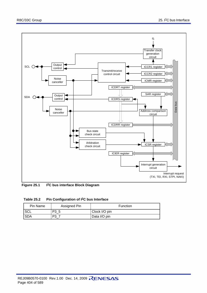
R8C/33C Group 25. I2C bus Interface
REJ09B0570-0100 Rev.1.00 Dec. 14, 2009Page 404 of 589
Figure 25.1 I2C bus interface Block Diagram
Table 25.2 Pin Configuration of I2C bus Interface
Pin Name Assigned Pin FunctionSCL P3_5 Clock I/O pinSDA P3_7 Data I/O pin
ICCR1 register
Dat
a bu
s
ICCR2 register
ICMR register
ICDRT register
SAR register
ICSR register
Address comparisoncircuit
OutputcontrolSCL
Interrupt request(TXI, TEI, RXI, STPI, NAKI)
Transfer clockgeneration
circuit
ICDRS register
ICDRR register
Bus statecheck circuit
Arbitrationcheck circuit
ICIER register
Interrupt generationcircuit
Transmit/receivecontrol circuit
Noisecanceller
SDA Outputcontrol
f1
Noisecanceller

R8C/33C Group 25. I2C bus Interface
REJ09B0570-0100 Rev.1.00 Dec. 14, 2009Page 405 of 589
Figure 25.2 External Circuit Connection Example of Pins SCL and SDA
SCL
SDA
SCL input
SCL output
SDA input
SDA output
(Master)
VCC VCC
SCL
SDA
SCL input
SCL output
SDA input
SDA output
(Slave 1)
SCL
SDA
SCL input
SCL output
SDA input
SDA output
SCL
SDA
(Slave 2)

R8C/33C Group 25. I2C bus Interface
REJ09B0570-0100 Rev.1.00 Dec. 14, 2009Page 406 of 589
25.2 Registers
25.2.1 Module Standby Control Register (MSTCR)
Notes:1. When the MSTIIC bit is set to 1 (standby), any access to the SSU or the I2C bus associated registers (addresses
0193h to 019Dh) is disabled.2. When the MSTTRC bit is set to 1 (standby), any access to the timer RC associated registers (addresses 0120h
to 0133h) is disabled.
Address 0008hBit b7 b6 b5 b4 b3 b2 b1 b0
Symbol — — MSTTRC MSTTRD MSTIIC — — —After Reset 0 0 0 0 0 0 0 0
Bit Symbol Bit Name Function R/Wb0 — Nothing is assigned. If necessary, set to 0. When read, the content is 0. —b1 —b2 —b3 MSTIIC SSU, I2C bus standby bit 0: Active
1: Standby (1)R/W
b4 MSTTRD Power consumption reduce bit Set to 1. The power consumption can be reduced.
R/W
b5 MSTTRC Timer RC standby bit 0: Active1: Standby (2)
R/W
b6 — Nothing is assigned. If necessary, set to 0. When read, the content is 0. —b7 —

R8C/33C Group 25. I2C bus Interface
REJ09B0570-0100 Rev.1.00 Dec. 14, 2009Page 407 of 589
25.2.2 SSU/IIC Pin Select Register (SSUIICSR)
Address 018ChBit b7 b6 b5 b4 b3 b2 b1 b0
Symbol — — — — — — — IICSELAfter Reset 0 0 0 0 0 0 0 0
Bit Symbol Bit Name Function R/Wb0 IICSEL SSU/I2C bus switch bit 0: SSU function selected
1: I2C bus function selectedR/W
b1 — Reserved bit Set to 0. R/Wb2 — Nothing is assigned. If necessary, set to 0. When read, the content is 0. —b3 —b4 — Reserved bits Set to 0. R/Wb5 —b6 —b7 —
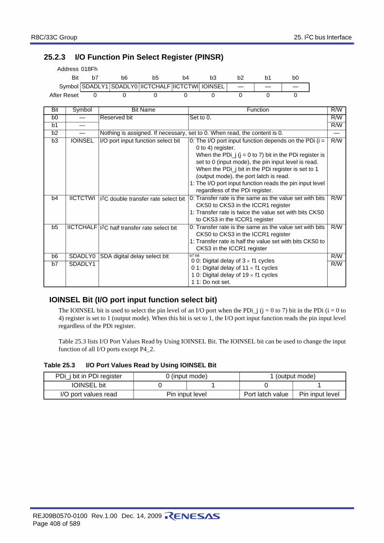
R8C/33C Group 25. I2C bus Interface
REJ09B0570-0100 Rev.1.00 Dec. 14, 2009Page 408 of 589
25.2.3 I/O Function Pin Select Register (PINSR)
IOINSEL Bit (I/O port input function select bit)The IOINSEL bit is used to select the pin level of an I/O port when the PDi_j (j = 0 to 7) bit in the PDi (i = 0 to4) register is set to 1 (output mode). When this bit is set to 1, the I/O port input function reads the pin input levelregardless of the PDi register.
Table 25.3 lists I/O Port Values Read by Using IOINSEL Bit. The IOINSEL bit can be used to change the inputfunction of all I/O ports except P4_2.
Address 018FhBit b7 b6 b5 b4 b3 b2 b1 b0
Symbol SDADLY1 SDADLY0 IICTCHALF IICTCTWI IOINSEL — — —After Reset 0 0 0 0 0 0 0 0
Bit Symbol Bit Name Function R/Wb0 — Reserved bit Set to 0. R/Wb1 — R/Wb2 — Nothing is assigned. If necessary, set to 0. When read, the content is 0. —b3 IOINSEL I/O port input function select bit 0: The I/O port input function depends on the PDi (i =
0 to 4) register.When the PDi_j (j = 0 to 7) bit in the PDi register is set to 0 (input mode), the pin input level is read. When the PDi_j bit in the PDi register is set to 1 (output mode), the port latch is read.
1: The I/O port input function reads the pin input level regardless of the PDi register.
R/W
b4 IICTCTWI I2C double transfer rate select bit 0: Transfer rate is the same as the value set with bits CKS0 to CKS3 in the ICCR1 register
1: Transfer rate is twice the value set with bits CKS0 to CKS3 in the ICCR1 register
R/W
b5 IICTCHALF I2C half transfer rate select bit 0: Transfer rate is the same as the value set with bits CKS0 to CKS3 in the ICCR1 register
1: Transfer rate is half the value set with bits CKS0 to CKS3 in the ICCR1 register
R/W
b6 SDADLY0 SDA digital delay select bit b7 b6 0 0: Digital delay of 3 × f1 cycles 0 1: Digital delay of 11 × f1 cycles 1 0: Digital delay of 19 × f1 cycles 1 1: Do not set.
R/Wb7 SDADLY1 R/W
Table 25.3 I/O Port Values Read by Using IOINSEL BitPDi_j bit in PDi register 0 (input mode) 1 (output mode)
IOINSEL bit 0 1 0 1I/O port values read Pin input level Port latch value Pin input level

R8C/33C Group 25. I2C bus Interface
REJ09B0570-0100 Rev.1.00 Dec. 14, 2009Page 409 of 589
25.2.4 IIC bus Transmit Data Register (ICDRT)
25.2.5 IIC bus Receive Data Register (ICDRR)
Address 0194hBit b7 b6 b5 b4 b3 b2 b1 b0
Symbol — — — — — — — —After Reset 1 1 1 1 1 1 1 1
Bit Function R/Wb7 to b0 This register stores transmit data.
When the ICDRS register is detected as empty, the stored transmit data item is transferred to the ICDRS register and data transmission starts.When the next unit of transmit data is written to the ICDRT register while data is transmitted to the ICDRS register, continuous transmission is enabled.When the MLS bit in the ICMR register is set to 1 (data transfer with LSB-first), the MSB-LSB inverted data is read after the data is written to the ICDRT register.
R/W
Address 0196hBit b7 b6 b5 b4 b3 b2 b1 b0
Symbol — — — — — — — —After Reset 1 1 1 1 1 1 1 1
Bit Function R/Wb7 to b0 This register stores receive data.
When the ICDRS register receives 1 byte of data, the receive data is transferred to the ICDRR register and the next receive operation is enabled.
R

R8C/33C Group 25. I2C bus Interface
REJ09B0570-0100 Rev.1.00 Dec. 14, 2009Page 410 of 589
25.2.6 IIC bus Control Register 1 (ICCR1)
Notes:1. Set according to the necessary transfer rate in master mode. Refer to Tables 25.4 and 25.5 Transfer Rate
Examples for the transfer rate. This bit is used for maintaining the setup time in transmit mode of slave mode. The time is 10Tcyc when the CKS3 bit is set to 0 and 20Tcyc when the CKS3 bit is set to 1. (1Tcyc = 1/f1(s))
2. Rewrite the TRS bit between transfer frames.3. When the first 7 bits after the start condition in slave receive mode match the slave address set in the SAR
register and the 8th bit is set to 1, the TRS bit is set to 1.4. In master mode with the I2C bus format, if arbitration is lost, bits MST and TRS are set to 0 and the IIC enters
slave receive mode.5. When an overrun error occurs in master receive mode with the clock synchronous serial format, the MST bit is
set to 0 and the I2C bus enters slave receive mode.6. In multimaster operation, use the MOV instruction to set bits TRS and MST.
Address 0198hBit b7 b6 b5 b4 b3 b2 b1 b0
Symbol ICE RCVD MST TRS CKS3 CKS2 CKS1 CKS0After Reset 0 0 0 0 0 0 0 0
Bit Symbol Bit Name Function R/Wb0 CKS0 Transmit clock select bits 3 to 0 (1) b3 b2 b1 b0
0 0 0 0: f1/28 0 0 0 1: f1/40 0 0 1 0: f1/48 0 0 1 1: f1/64 0 1 0 0: f1/80 0 1 0 1: f1/100 0 1 1 0: f1/112 0 1 1 1: f1/128 1 0 0 0: f1/56 1 0 0 1: f1/80 1 0 1 0: f1/96 1 0 1 1: f1/128 1 1 0 0: f1/160 1 1 0 1: f1/200 1 1 1 0: f1/224 1 1 1 1: f1/256
R/Wb1 CKS1 R/Wb2 CKS2 R/Wb3 CKS3 R/W
b4 TRS Transfer/receive select bit (2, 3, 6) b5 b4
0 0: Slave Receive Mode (4)
0 1: Slave Transmit Mode 1 0: Master Receive Mode 1 1: Master Transmit Mode
R/Wb5 MST Master/slave select bit (5, 6) R/W
b6 RCVD Receive disable bit After reading the ICDRR register while the TRS bit is set to 00: Next receive operation continues1: Next receive operation disabled
R/W
b7 ICE I2C bus interface enable bit 0: This module is halted(Pins SCL and SDA are set to a port function)
1: This module is enabled for transfer operations(Pins SCL and SDA are in a bus drive state)
R/W

R8C/33C Group 25. I2C bus Interface
REJ09B0570-0100 Rev.1.00 Dec. 14, 2009Page 411 of 589
25.2.7 IIC bus Control Register 2 (ICCR2)
Notes:1. When rewriting the SDAO bit, write 0 to the SDAOP bit simultaneously using the MOV instruction.2. Do not write to the SDAO bit during a transfer operation.3. Enabled in master mode. When writing to the BBSY bit, write 0 to the SCP bit simultaneously using the MOV
instruction. Execute the same way when a start condition is regenerated.4. Disabled when the clock synchronous serial format is used.
Address 0199hBit b7 b6 b5 b4 b3 b2 b1 b0
Symbol BBSY SCP SDAO SDAOP SCLO — IICRST —After Reset 0 1 1 1 1 1 0 1
Bit Symbol Bit Name Function R/Wb0 — Nothing is assigned. If necessary, set to 0. When read, the content is 1. —b1 IICRST I2C bus control block reset bit When hang-up occurs due to communication failure during
I2C bus interface operation, writing 1 resets the control block of the I2C bus interface without setting ports or initializing registers.
R/W
b2 — Nothing is assigned. If necessary, set to 0. When read, the content is 1. —b3 SCLO SCL monitor flag 0: SCL pin is set to “L”
1: SCL pin is set to “H”R
b4 SDAOP SDAO write protect bit When rewriting the SDAO bit, write 0 simultaneously (1).When read, the content is 1.
R/W
b5 SDAO SDA output value control bit When read0: SDA pin output is held “L”1: SDA pin output is held “H”When written (1, 2)
0: SDA pin output is changed to “L”1: SDA pin output is changed to high-impedance
(“H” output via external pull-up resistor)
R/W
b6 SCP Start/stop condition generation disable bit
When writing to the to BBSY bit, write 0 simultaneously (3).When read, the content is 1.Writing 1 is invalid.
R/W
b7 BBSY Bus busy bit (4) When read:0: Bus is released
(SDA signal changes from “L” to “H” while SCL signal is held “H”)
1: Bus is occupied(SDA signal changes from “H” to “L” while SCL signal is held “H”)
When written (3):0: Stop condition generated1: Start condition generated
R/W
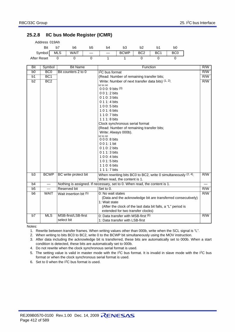
R8C/33C Group 25. I2C bus Interface
REJ09B0570-0100 Rev.1.00 Dec. 14, 2009Page 412 of 589
25.2.8 IIC bus Mode Register (ICMR)
Notes:1. Rewrite between transfer frames. When writing values other than 000b, write when the SCL signal is “L”.2. When writing to bits BC0 to BC2, write 0 to the BCWP bit simultaneously using the MOV instruction.3. After data including the acknowledge bit is transferred, these bits are automatically set to 000b. When a start
condition is detected, these bits are automatically set to 000b.4. Do not rewrite when the clock synchronous serial format is used.5. The setting value is valid in master mode with the I2C bus format. It is invalid in slave mode with the I2C bus
format or when the clock synchronous serial format is used.6. Set to 0 when the I2C bus format is used.
Address 019AhBit b7 b6 b5 b4 b3 b2 b1 b0
Symbol MLS WAIT — — BCWP BC2 BC1 BC0After Reset 0 0 0 1 1 0 0 0
Bit Symbol Bit Name Function R/Wb0 BC0 Bit counters 2 to 0 I2C bus format
(Read: Number of remaining transfer bits; Write: Number of next transfer data bits) (1, 2).b2 b1 b0
0 0 0: 9 bits (3)
0 0 1: 2 bits 0 1 0: 3 bits 0 1 1: 4 bits 1 0 0: 5 bits 1 0 1: 6 bits 1 1 0: 7 bits 1 1 1: 8 bitsClock synchronous serial format (Read: Number of remaining transfer bits; Write: Always 000b).b2 b1 b0 0 0 0: 8 bits 0 0 1: 1 bit 0 1 0: 2 bits 0 1 1: 3 bits 1 0 0: 4 bits 1 0 1: 5 bits 1 1 0: 6 bits 1 1 1: 7 bits
R/Wb1 BC1 R/Wb2 BC2 R/W
b3 BCWP BC write protect bit When rewriting bits BC0 to BC2, write 0 simultaneously (2, 4).When read, the content is 1.
R/W
b4 — Nothing is assigned. If necessary, set to 0. When read, the content is 1. —b5 — Reserved bit Set to 0. R/Wb6 WAIT Wait insertion bit (5) 0: No wait states
(Data and the acknowledge bit are transferred consecutively)1: Wait state
(After the clock of the last data bit falls, a “L” period is extended for two transfer clocks)
R/W
b7 MLS MSB-first/LSB-first select bit
0: Data transfer with MSB-first (6)
1: Data transfer with LSB-firstR/W

R8C/33C Group 25. I2C bus Interface
REJ09B0570-0100 Rev.1.00 Dec. 14, 2009Page 413 of 589
25.2.9 IIC bus Interrupt Enable Register (ICIER)
Notes:1. An overrun error interrupt request is generated when the clock synchronous format is used.2. Set the STIE bit to 1 (stop condition detection interrupt request enabled) when the STOP bit in the ICSR register
is set to 0.
Address 019BhBit b7 b6 b5 b4 b3 b2 b1 b0
Symbol TIE TEIE RIE NAKIE STIE ACKE ACKBR ACKBTAfter Reset 0 0 0 0 0 0 0 0
Bit Symbol Bit Name Function R/Wb0 ACKBT Transmit acknowledge
select bit0: In receive mode, 0 is transmitted as the acknowledge bit.1: In receive mode, 1 is transmitted as the acknowledge bit.
R/W
b1 ACKBR Receive acknowledge bit 0: In transmit mode, the acknowledge bit received from receive device is set to 0.
1: In transmit mode, the acknowledge bit received from receive device is set to 1.
R
b2 ACKE Acknowledge bit detection select bit
0: Content of the receive acknowledge bit is ignored and continuous transfer is performed.
1: When the receive acknowledge bit is set to 1, continuous transfer is halted.
R/W
b3 STIE Stop condition detection interrupt enable bit
0: Stop condition detection interrupt request disabled1: Stop condition detection interrupt request enabled (2)
R/W
b4 NAKIE NACK receive interrupt enable bit
0: NACK receive interrupt request and arbitration lost/ overrun error interrupt request disabled
1: NACK receive interrupt request and arbitration lost/ overrun error interrupt request (1)
R/W
b5 RIE Receive interrupt enable bit 0: Receive data full and overrun error interrupt request disabled
1: Receive data full and overrun error interrupt request enabled (1)
R/W
b6 TEIE Transmit end interrupt enable bit
0: Transmit end interrupt request disabled1: Transmit end interrupt request enabled
R/W
b7 TIE Transmit interrupt enable bit 0: Transmit data empty interrupt request disabled1: Transmit data empty interrupt request enabled
R/W

R8C/33C Group 25. I2C bus Interface
REJ09B0570-0100 Rev.1.00 Dec. 14, 2009Page 414 of 589
25.2.10 IIC bus Status Register (ICSR)
Notes:1. Each bit is set to 0 by reading 1 before writing 0.2. This flag is enabled in slave receive mode with the I2C bus format.3. When two or more master devices attempt to occupy the bus at nearly the same time, if the I2C bus Interface
monitors the SDA pin and the data which the I2C bus Interface transmits is different, the AL flag is set to 1 andthe bus is occupied by another master.
4. The NACKF bit is enabled when the ACKE bit in the ICIER register is set to 1 (when the receive acknowledge bitis set to 1, transfer is halted).
5. The RDRF bit is set to 0 when data is read from the ICDRR register.6. Bits TEND and TDRE are set to 0 when data is written to the ICDRT register.
When accessing the ICSR register continuously, insert one or more NOP instructions between the instructionsto access it.
Address 019ChBit b7 b6 b5 b4 b3 b2 b1 b0
Symbol TDRE TEND RDRF NACKF STOP AL AAS ADZAfter Reset 0 0 0 0 X 0 0 0
Bit Symbol Bit Name Function R/Wb0 ADZ General call address
recognition flag (1, 2)This flag is set to 1 when a general call address is detected.
R/W
b1 AAS Slave address recognition flag (1)
This flag is set to 1 when the first frame immediately after the start condition matches bits SVA0 to SVA6 in the SAR register in slave receive mode (slave address detection and general call address detection)
R/W
b2 AL Arbitration lost flag/overrun error flag (1)
I2C bus format: This flag indicates that arbitration has been lost in master mode. This flag is set to 1 (3) when:
• The internal SDA signal and SDA pin level do not match at the rising edge of the SCL signal in master transmit mode
• The SDA pin is held “H” at start condition detection in master transmit/receive mode
Clock synchronous format: This flag indicates an overrun error. This flag is set to 1 when:
• The last bit of the next unit of data is received while the RDRF bit is set to 1
R/W
b3 STOP Stop condition detection flag (1) This flag is set to 1 when a stop condition is detected after the frame is transferred.
R/W
b4 NACKF No acknowledge detection flag (1, 4)
This flag is set to 1 when no ACKnowledge is detected from the receive device after transmission.
R/W
b5 RDRF Receive data register full flag (1, 5)
This flag is set to 1 when receive data is transferred from registers ICDRS to ICDRR.
R/W
b6 TEND Transmit end flag (1, 6) I2C bus format: This flag is set to 1 at the rising edge of the 9th clock cycle of the SCL signal while the TDRE bit is set to 1.Clock synchronous format: This flag is set to 1 when the last bit of the transmit frame is transmitted.
R/W
b7 TDRE Transmit data empty flag (1, 6) This flag is set to 1 when:• Data is transferred from registers ICDRT to ICDRS and
the CDRT register is empty• The TRS bit in the ICCR1 register is set to 1 (transmit
mode)• A start condition is generated (including retransmission)• Slave receive mode is changed to slave transmit mode
R/W

R8C/33C Group 25. I2C bus Interface
REJ09B0570-0100 Rev.1.00 Dec. 14, 2009Page 415 of 589
25.2.11 Slave Address Register (SAR)
25.2.12 IIC bus Shift Register (ICDRS)
Address 019DhBit b7 b6 b5 b4 b3 b2 b1 b0
Symbol SVA6 SVA5 SVA4 SVA3 SVA2 SVA1 SVA0 FSAfter Reset 0 0 0 0 0 0 0 0
Bit Symbol Bit Name Function R/Wb0 FS Format select bit 0: I2C bus format
1: Clock synchronous serial formatR/W
b1 SVA0 Slave addresses 6 to 0 Set an address different from that of the other slave devices connected to the I2C bus. When the 7 high-order bits of the first frame transmitted after the start condition match bits SVA0 to SVA6 in slave mode of the I2C bus format, the MCU operates as a slave device.
R/Wb2 SVA1 R/Wb3 SVA2 R/Wb4 SVA3 R/Wb5 SVA4 R/Wb6 SVA5 R/Wb7 SVA6 R/W
Bit b7 b6 b5 b4 b3 b2 b1 b0Symbol — — — — — — — —
Bit Function R/Wb7 to b0 This register transmits and receives data.
During transmission, data is transferred from registers ICRDT to ICDRS and transmitted from the SDA pin.During reception, data is transferred from registers ICDRS to the ICDRR after 1 byte of data reception ends.
—

R8C/33C Group 25. I2C bus Interface
REJ09B0570-0100 Rev.1.00 Dec. 14, 2009Page 416 of 589
25.3 Common Items for Multiple Modes
25.3.1 Transfer ClockWhen the MST bit in the ICCR1 register is set to 0, the transfer clock is the external clock input from the SCLpin. When the MST bit in the ICCR1 register is set to 1, the transfer clock is the internal clock selected by bits CKS0to CKS3 in the ICCR1 register and bits IICTCTWI and IICTCHALF in the PINSR register and the transferclock is output from the SCL pin.Table 25.4 lists the Transfer Rate Examples (1).
Table 25.4 Transfer Rate Examples (1)PINSR Register ICCR1 Register Transfer
ClockTransfer Rate
IICTCHALF IICTCTWI CKS3 CKS2 CKS1 CKS0 f1 = 5 MHz f1 = 8 MHz f1 = 10 MHz f1 = 16 MHz f1 = 20 MHz0 0 0 0 0 0 f1/28 179 kHz 286 kHz 357 kHz 571 kHz 714 kHz
1 f1/40 125 kHz 200 kHz 250 kHz 400 kHz 500 kHz1 0 f1/48 104 kHz 167 kHz 208 kHz 333 kHz 417 kHz
1 f1/64 78.1 kHz 125 kHz 156 kHz 250 kHz 313 kHz1 0 0 f1/80 62.5 kHz 100 kHz 125 kHz 200 kHz 250 kHz
1 f1/100 50.0 kHz 80.0 kHz 100 kHz 160 kHz 200 kHz1 0 f1/112 44.6 kHz 71.4 kHz 89.3 kHz 143 kHz 179 kHz
1 f1/128 39.1 kHz 62.5 kHz 78.1 kHz 125 kHz 156 kHz1 0 0 0 f1/56 89.3 kHz 143 kHz 179 kHz 286 kHz 357 kHz
1 f1/80 62.5 kHz 100 kHz 125 kHz 200 kHz 250 kHz1 0 f1/96 52.1 kHz 83.3 kHz 104 kHz 167 kHz 208 kHz
1 f1/128 39.1 kHz 62.5 kHz 78.1 kHz 125 kHz 156 kHz1 0 0 f1/160 31.3 kHz 50.0 kHz 62.5 kHz 100 kHz 125 kHz
1 f1/200 25.0 kHz 40.0 kHz 50.0 kHz 80.0 kHz 100 kHz1 0 f1/224 22.3 kHz 35.7 kHz 44.6 kHz 71.4 kHz 89.3 kHz
1 f1/256 19.5 kHz 31.3 kHz 39.1 kHz 62.5 kHz 78.1 kHz

R8C/33C Group 25. I2C bus Interface
REJ09B0570-0100 Rev.1.00 Dec. 14, 2009Page 417 of 589
Table 25.5 Transfer Rate Examples (2)PINSR Register ICCR1 Register Transfer
ClockTransfer Rate
IICTCHALF IICTCTWI CKS3 CKS2 CKS1 CKS0 f1 = 5 MHz f1 = 8 MHz f1 = 10 MHz f1 = 16 MHz f1 = 20 MHz0 1 0 0 0 0 f1/28 358 kHz 572 kHz 714 kHz 1142 kHz 1428 kHz
1 f1/40 250 kHz 400 kHz 500 kHz 800 kHz 1000 kHz1 0 f1/48 208 kHz 334 kHz 416 kHz 666 kHz 834 kHz
1 f1/64 156 kHz 250 kHz 312 kHz 500 kHz 626 kHz1 0 0 f1/80 125 kHz 200 kHz 250 kHz 400 kHz 500 kHz
1 f1/100 100 kHz 160 kHz 200 kHz 320 kHz 400 kHz1 0 f1/112 89 kHz 143 kHz 179 kHz 286 kHz 358 kHz
1 f1/128 78 kHz 125 kHz 156 kHz 250 kHz 312 kHz1 0 0 0 f1/56 179 kHz 286 kHz 358 kHz 572 kHz 714 kHz
1 f1/80 125 kHz 200 kHz 250 kHz 400 kHz 500 kHz1 0 f1/96 104 kHz 167 kHz 208 kHz 334 kHz 416 kHz
1 f1/128 78 kHz 125 kHz 156 kHz 250 kHz 312 kHz1 0 0 f1/160 63 kHz 100 kHz 125 kHz 200 kHz 250 kHz
1 f1/200 50 kHz 80 kHz 100 kHz 160 kHz 200 kHz1 0 f1/224 45 kHz 71 kHz 89 kHz 143 kHz 179 kHz
1 f1/256 39 kHz 63 kHz 78 kHz 125 kHz 156 kHz1 0 0 0 0 0 f1/28 90 kHz 143 kHz 179 kHz 286 kHz 357 kHz
1 f1/40 63 kHz 100 kHz 125 kHz 200 kHz 250 kHz1 0 f1/48 52 kHz 84 kHz 104 kHz 167 kHz 209 kHz
1 f1/64 39 kHz 63 kHz 78 kHz 125 kHz 157 kHz1 0 0 f1/80 31 kHz 50 kHz 63 kHz 100 kHz 125 kHz
1 f1/100 25 kHz 40 kHz 50 kHz 80 kHz 100 kHz1 0 f1/112 22 kHz 36 kHz 45 kHz 72 kHz 90 kHz
1 f1/128 20 kHz 31 kHz 39 kHz 63 kHz 78 kHz1 0 0 0 f1/56 45 kHz 72 kHz 90 kHz 143 kHz 179 kHz
1 f1/80 31 kHz 50 kHz 63 kHz 100 kHz 125 kHz1 0 f1/96 26 kHz 42 kHz 52 kHz 84 kHz 104 kHz
1 f1/128 20 kHz 31 kHz 39 kHz 63 kHz 78 kHz1 0 0 f1/160 16 kHz 25 kHz 31 kHz 50 kHz 63 kHz
1 f1/200 13 kHz 20 kHz 25 kHz 40 kHz 50 kHz1 0 f1/224 11 kHz 18 kHz 22 kHz 36 kHz 45 kHz
1 f1/256 10 kHz 16 kHz 20 kHz 31 kHz 39 kHz

R8C/33C Group 25. I2C bus Interface
REJ09B0570-0100 Rev.1.00 Dec. 14, 2009Page 418 of 589
25.3.2 SDA Pin Digital Delay SelectionThe digital delay value for the SDA pin can be selected by bits SDADLY0 to SDADLY1 in the PINSR register.Figure 25.3 shows the Operating Example of Digital Delay for SDA Pin.
Figure 25.3 Operating Example of Digital Delay for SDA Pin
20 µs (Transfer Rate = 50 kHz)
SCL
SDADLY0 to SDADLY1: Bits in PINSR register
• SDADLY1 to SDADLY0 = 00b(3 × f1 cycles)
3 × f1 cycles
SDA
300 ns (f1 = 10 MHz)
• SDADLY1 to SDADLY0 = 01b(11 × f1 cycles)
11 × f1 cycles
SDA
1.1 µs (f1 = 10 MHz)
• SDADLY1 to SDADLY0 = 10b(19 × f1 cycles)
19 × f1 cycles
SDA
0.95 µs (f1 = 20 MHz)

R8C/33C Group 25. I2C bus Interface
REJ09B0570-0100 Rev.1.00 Dec. 14, 2009Page 419 of 589
25.3.3 Interrupt RequestsThe I2C bus interface has six interrupt requests when the I2C bus format is used and four interrupt requests whenthe clock synchronous serial format is used.Table 25.6 lists the Interrupt Requests of I2C bus Interface.Because these interrupt requests are allocated at the I2C bus interface interrupt vector table, the source must bedetermined bit by bit.
STIE, NAKIE, RIE, TEIE, TIE: Bits in ICIER registerAL, STOP, NACKF, RDRF, TEND, TDRE: Bits in ICSR register
When generation conditions listed in Table 25.6 are met, an I2C bus interface interrupt request is generated. Setthe interrupt generation conditions to 0 by the I2C bus interface interrupt routine. Note that bits TDRE and TEND are automatically set to 0 by writing transmit data to the ICDRT register andthat the RDRF bit is automatically set to 0 by reading the ICDRR register. Especially, the TDRE bit is set to 0when writing transmit data to the ICDRT register and set to 1 when transferring data from the ICDRT register tothe ICDRS register. If the TDRE bit is further set to 0, additional 1 byte may be transmitted.Also, set the STIE bit to 1 (stop condition detection interrupt request enabled) when the STOP bit is set to 0.
Table 25.6 Interrupt Requests of I2C bus Interface
Interrupt Request Generation Condition
Format
I2C busClock
Synchronous Serial
Transmit data empty TXI TIE = 1 and TDRE = 1 Enabled EnabledTransmit ends TEI TEIE = 1 and TEND = 1 Enabled EnabledReceive data full RXI RIE = 1 and RDRF = 1 Enabled EnabledStop condition detection STPI STIE = 1 and STOP = 1 Enabled DisabledNACK detection NAKI NAKIE = 1 and AL = 1
(or NAKIE = 1 and NACKF = 1)Enabled Disabled
Arbitration lost/overrun error Enabled Enabled

R8C/33C Group 25. I2C bus Interface
REJ09B0570-0100 Rev.1.00 Dec. 14, 2009Page 420 of 589
25.4 I2C bus Interface Mode
25.4.1 I2C bus FormatWhen the FS bit in the SAR register is set to 0, the I2C bus format is used for communication.Figure 25.4 shows the I2C bus Format and Bus Timing. The first frame following the start condition consists of8 bits.
Figure 25.4 I2C bus Format and Bus Timing
S R/W A DATA A A/A P
1 7 1 1 n 1 1 1
1 m
(a) I2C bus format (FS = 0)
Number of transfer bits (n = 1 to 8)
Number of transfer frames (m = 1 or more)
S R/W A DATA A/A P
1 7 1 1 n1 1 1
1 m1
(b) I2C bus format When Start Condition is Retransmitted (FS = 0)
Upper: Number of transfer bits (n1, n2 = 1 to 8)Lower: Number of transfer frames (m1, m2 = 1 or more)
SLA
SLA A/A
1
S
1
R/W A DATA
7 1 1 n2
SLA
1 m2
SDA
SCL
S SLA R/W A DATA A DATA A P
1 to 7 8 9 1 to 7 8 9 1 to 7 8 9
(1) I2C bus format
(2) I2C bus timing
Legend:S : Start condition The master device changes the SDA signal from “H” to “L” while the SCL signal is held “H”.SLA : Slave addressR/W : Indicates the direction of data transmission/reception Data is transmitted when: R/W value is 1: From the slave device to the master device R/W value is 0: From the master device to the slave deviceA : Acknowledge The receive device sets the SDA signal to “L”.DATA : Transmit/receive dataP : Stop condition The master device changes the SDA signal from “L” to “H” while the SCL signal is held “H”.

R8C/33C Group 25. I2C bus Interface
REJ09B0570-0100 Rev.1.00 Dec. 14, 2009Page 421 of 589
25.4.2 Master Transmit OperationIn master transmit mode, the master device outputs the transmit clock and data, and the slave device returns anacknowledge signal.Figures 25.5 and 25.6 show the Operating Timing in Master Transmit Mode (I2C bus Interface Mode).
The transmit procedure and operation in master transmit mode are as follows.(1) Set the STOP bit in the ICSR register to 0 for initialization, and set the ICE bit in the ICCR1 register to 1
(transfer operation enabled). Then, set bits WAIT and MLS in the ICMR register and bits CKS0 to CKS3 inthe ICCR1 register (initial setting).
(2) After confirming that the bus is released by reading the BBSY bit in the ICCR2 register, set bits TRS andMST in the ICCR1 register to master transmit mode. Then, write 1 to the BBSY bit and 0 to the SCP bitwith the MOV instruction (start condition generated). This will generate a start condition.
(3) After confirming that the TDRE bit in the ICSR register is set to 1 (data is transferred from registers ICDRTto ICDRS), write transmit data to the ICDRT register (data in which a slave address and R/W are indicatedin the 1st byte). At this time, the TDRE bit is automatically set to 0. When data is transferred from registersICDRT to ICDRS, the TDRE bit is set to 1 again.
(4) When 1 byte of data transmission is completed while the TDRE bit is set to 1, the TEND bit in the ICSRregister is set to 1 at the rising edge of the 9th clock cycle of the transmit clock. After confirming that theslave device is selected by reading the ACKBR bit in the ICIER register, write the 2nd byte of data to theICDRT register. Since the slave device is not acknowledged when the ACKBR bit is set to 1, generate astop condition. Stop condition generation is enabled by writing 0 to the BBSY bit and 0 to the SCP bit withthe MOV instruction. The SCL signal is fixed “L” until data is ready or a stop condition is generated.
(5) Write the transmit data after the 2nd byte to the ICDRT register every time the TDRE bit is set to 1.(6) When the number of bytes to be transmitted is written to the ICDRT register, wait until the TEND bit is set
to 1 while the TDRE bit is set to 1. Or wait for NACK (NACKF bit in ICSR register = 1) from the receivedevice while the ACKE bit in the ICIER register is set to 1 (when the receive acknowledge bit is set to 1,transfer is halted). Then, generate a stop condition before setting the TEND bit or the NACKF bit to 0.
(7) When the STOP bit in the ICSR register is set to 1, return to slave receive mode.

R8C/33C Group 25. I2C bus Interface
REJ09B0570-0100 Rev.1.00 Dec. 14, 2009Page 422 of 589
Figure 25.5 Operating Timing in Master Transmit Mode (I2C bus Interface Mode) (1)
Figure 25.6 Operating Timing in Master Transmit Mode (I2C bus Interface Mode) (2)
SDA(master output)
SCL(master output) 1 2 8 96 74 53
b7 b6 b5 b4 b3 b2 b1 b0 b7 b6
1 2
SDA(slave output)
TDRE bit inICSR register
TEND bit inICSR register
ICDRT register
ICDRS register
R/WSlave address
Address + R/W
Program processing (2) Instruction forstart conditiongeneration
(3) Write data to ICDRT register(1st byte).
A
(4) Write data to ICDRT register(2nd byte).
(5) Write data to ICDRT register(3rd byte).
Data 2
Address + R/W
Data 1
Data 1
SDA(master output)
SCL(master output) 1 2 8 96 74 53
b7 b6 b5 b4 b3 b2 b1 b0
SDA(slave output)
TDRE bit inICSR register
TEND bit inICSR register
ICDRT register
ICDRS register
Data n
Program processing (6) Generate a stop conditionand set TEND bit to 0.
(3) Write data to ICDRT register.
A/A
(7) Set to slave receive mode.
9
A
Data n

R8C/33C Group 25. I2C bus Interface
REJ09B0570-0100 Rev.1.00 Dec. 14, 2009Page 423 of 589
25.4.3 Master Receive OperationIn master receive mode, the master device outputs the receive clock, receives data from the slave device, andreturns an acknowledge signal.Figures 25.7 and 25.8 show the Operating Timing in Master Receive Mode (I2C bus Interface Mode). The receive procedure and operation in master receive mode are shown below.(1) After setting the TEND bit in the ICSR register to 0, set the TRS bit in the ICCR1 register to 0 to switch
from master transmit mode to master receive mode. Then set the TDRE bit in the ICSR register to 0.(2) Dummy reading the ICDRR register starts receive operation. The receive clock is output in synchronization
with the internal clock and data is received. The master device outputs the level set by the ACKBT bit inthe ICIER register to the SDA pin at the rising edge of the 9th clock cycle of the receive clock.
(3) When 1-frame of data reception is completed, the RDRF bit in the ICSR register is set to 1 at the risingedge of the 9th clock cycle of the receive clock. At this time, if the ICDRR register is read, the receiveddata can be read and the RDRF bit is set to 0 simultaneously.
(4) Continuous receive operation is enabled by reading the ICDRR register every time the RDRF bit is set to 1.If reading the ICDRR register is delayed by another process and the 8th clock cycle falls while the RDRFbit is set to 1, the SCL signal is fixed “L” until the ICDRR register is read.
(5) If the next frame is the last receive frame and the RCVD bit in the ICCR1 register is set to 1 (next receiveoperation disabled) before reading the ICDRR register, stop condition generation is enabled after the nextreceive operation.
(6) When the RDRF bit is set to 1 at the rising edge of the 9th clock cycle of the receive clock, generate a stopcondition.
(7) When the STOP bit in the ICSR register is set to 1, read the ICDRR register and set the RCVD bit to 0 (nextreceive operation continues).
(8) Return to slave receive mode.

R8C/33C Group 25. I2C bus Interface
REJ09B0570-0100 Rev.1.00 Dec. 14, 2009Page 424 of 589
Figure 25.7 Operating Timing in Master Receive Mode (I2C bus Interface Mode) (1)
SDA(master output)
SCL(master output) 189 6 74 53
b7 b6 b5 b4 b3 b2 b1 b0 b7
1 2
SDA(slave output)
TDRE bit inICSR register
TEND bit inICSR register
ICDRR register
ICDRS register Data 1
Program processing (1) After setting bits TEND and TRS to 0,set TDRE bit to 0.
A
(2) Read ICDRR register.
Data 1
9
TRS bit inICCR1 register
RDRF bit inICSR register
A
(3) Read ICDRR register.
Master transmit mode Master receive mode

R8C/33C Group 25. I2C bus Interface
REJ09B0570-0100 Rev.1.00 Dec. 14, 2009Page 425 of 589
Figure 25.8 Operating Timing in Master Receive Mode (I2C bus Interface Mode) (2)
SDA(master output)
SCL(master output) 1 2 8 96 74 53
b7 b6 b5 b4 b3 b2 b1 b0SDA(slave output)
RCVD bit inICCR1 register
ICDRR register
ICDRS register Data n-1
Program processing (6) Generate a stop condition.
A/A
(8) Set to slave receive mode.
9
A
Data n
RDRF bit inICSR register
Data n
Data n-1
(5) Read ICDRR registerafter setting RCVD bit to 1.
(7) Set RCVD bit to 0after reading ICDRR register.

R8C/33C Group 25. I2C bus Interface
REJ09B0570-0100 Rev.1.00 Dec. 14, 2009Page 426 of 589
25.4.4 Slave Transmit OperationIn slave transmit mode, the slave device outputs the transmit data while the master device outputs the receiveclock and returns an acknowledge signal.Figures 25.9 and 25.10 show the Operating Timing in Slave Transmit Mode (I2C bus Interface Mode).
The transmit procedure and operation in slave transmit mode are as follows.(1) Set the ICE bit in the ICCR1 register to 1 (transfer operation enabled), and set bits WAIT and MLS in the
ICMR register and bits CKS0 to CKS3 in the ICCR1 register (initial setting). Then, set bits TRS and MSTin the ICCR1 register to 0 and wait until the slave address matches in slave receive mode.
(2) When the slave address matches at the first frame after detecting the start condition, the slave deviceoutputs the level set by the ACKBT bit in the ICIER register to the SDA pin at the rising edge of the 9thclock cycle. At this time, if the 8th bit of data (R/W) is 1, bits TRS and TDRE in the ICSR register are set to1, and the mode is switched to slave transmit mode automatically. Continuous transmission is enabled bywriting transmit data to the ICDRT register every time the TDRE bit is set to 1.
(3) When the TDRE bit in the ICDRT register is set to 1 after the last transmit data is written to the ICDRTregister, wait until the TEND bit in the ICSR register is set to 1 while the TDRE bit is set to 1. When theTEND bit is set to 1, set the TEND bit to 0.
(4) Set the TRS bit to 0 and dummy read the ICDRR register to end the process. This will release the SCLsignal.
(5) Set the TDRE bit to 0.

R8C/33C Group 25. I2C bus Interface
REJ09B0570-0100 Rev.1.00 Dec. 14, 2009Page 427 of 589
Figure 25.9 Operating Timing in Slave Transmit Mode (I2C bus Interface Mode) (1)
SDA(master output)
SCL(master output) 189 6 74 53
b7 b6 b5 b4 b3 b2 b1 b0 b7
1 2
SDA(slave output)
TDRE bit inICSR register
TEND bit inICSR register
0
ICDRR register
ICDRS register Data 1
Program Processing
A
Data 2
9
TRS bit inICCR1 register
A
Slave transmit modeSlave receive mode
SCL(slave output)
ICDRT register Data 1
(1) Write data to ICDRT register(data 1).
(2) Write data to ICDRT register(data 2).
Data 2
(2) Write Data to ICDRT register(data 3).
Data 3

R8C/33C Group 25. I2C bus Interface
REJ09B0570-0100 Rev.1.00 Dec. 14, 2009Page 428 of 589
Figure 25.10 Operating Timing in Slave Transmit Mode (I2C bus Interface Mode) (2)
SDA(slave output)
SCL(master output) 1 2 8 96 74 53
b7 b6 b5 b4 b3 b2 b1 b0
SDA(master output)
TDRE bit inICSR register
TEND bit inICSR register
ICDRT register
ICDRS register
Data n
Program processing (3) Set TEND bit to 0.
A
9
A
Data n
Slave receivemode
Slave transmit mode
TRS bit inICCR1 register
ICDRR register
(4) Dummy read ICDRR registerafter setting TRS bit to 0. (5) Set TDRE bit to 0.
SCL(slave output)

R8C/33C Group 25. I2C bus Interface
REJ09B0570-0100 Rev.1.00 Dec. 14, 2009Page 429 of 589
25.4.5 Slave Receive OperationIn slave receive mode, the master device outputs the transmit clock and data, and the slave device returns anacknowledge signal.Figures 25.11 and 25.12 show the Operating Timing in Slave Receive Mode (I2C bus Interface Mode).
The receive procedure and operation in slave receive mode are as follows.(1) Set the ICE bit in the ICCR1 register to 1 (transfer operation enabled), and set bits WAIT and MLS in the
ICMR register and bits CKS0 to CKS3 in the ICCR1 register (initial setting). Then, set bits TRS and MSTin the ICCR1 register to 0 and wait until the slave address matches in slave receive mode.
(2) When the slave address matches at the first frame after detecting the start condition, the slave deviceoutputs the level set in the ACKBT bit in the ICIER register to the SDA pin at the rising edge of the 9thclock cycle. Since the RDRF bit in the ICSR register is set to 1 simultaneously, dummy read the ICDRRregister (the read data is unnecessary because it indicates the slave address and R/W).
(3) Read the ICDRR register every time the RDRF bit is set to 1. If the 8th clock cycle falls while the RDRF bitis set to 1, the SCL signal is fixed “L” until the ICDRR register is read. The setting change of theacknowledge signal returned to the master device before reading the ICDRR register takes affect from thefollowing transfer frame.
(4) Reading the last byte is also performed by reading the ICDRR register.

R8C/33C Group 25. I2C bus Interface
REJ09B0570-0100 Rev.1.00 Dec. 14, 2009Page 430 of 589
Figure 25.11 Operating Timing in Slave Receive Mode (I2C bus Interface Mode) (1)
Figure 25.12 Operating Timing in Slave Receive Mode (I2C bus Interface Mode) (2)
SDA(master output)
SCL(master output) 189 6 74 53
b7 b6 b5 b4 b3 b2 b1 b0 b7
1 2
SDA(slave output)
ICDRR register
ICDRS register Data 1
Program processing
A
(2) Dummy read ICDRR register.
Data 1
9
RDRF bit inICSR register
A
(2) Read ICDRR register.
SCL(slave output)
Data 2
SDA(master output)
SCL(master output) 89 6 74 53
b7 b6 b5 b4 b3 b2 b1 b0
1 2
SDA(slave output)
ICDRR register
ICDRS register Data 1
Program processing
A
(3) Read ICDRR register.
Data 1
9
RDRF bit inICSR register
A
(4) Read ICDRR register.
SCL(slave output)
Data 2
(3) Set ACKBT bit to 1.

R8C/33C Group 25. I2C bus Interface
REJ09B0570-0100 Rev.1.00 Dec. 14, 2009Page 431 of 589
25.5 Clock Synchronous Serial Mode
25.5.1 Clock Synchronous Serial FormatWhen the FS bit in the SAR register is set to 1, the clock synchronous serial format is used for communication.Figure 25.13 shows the Transfer Format of Clock Synchronous Serial Format. When the MST bit in the ICCR1 register is set to 1, the transfer clock is output from the SCL pin. When theMST bit is set to 0, the external clock is input. The transfer data is output between successive falling edges of the SCL clock, and data is determined at therising edge of the SCL clock. MSB-first or LSB-first can be selected as the order of the data transfer by settingthe MLS bit in the ICMR register. The SDA output level can be changed by the SDAO bit in the ICCR2 registerduring transfer standby.
Figure 25.13 Transfer Format of Clock Synchronous Serial Format
SCL
b0SDA b1 b2 b3 b4 b5 b6 b7

R8C/33C Group 25. I2C bus Interface
REJ09B0570-0100 Rev.1.00 Dec. 14, 2009Page 432 of 589
25.5.2 Transmit OperationIn transmit mode, transmit data is output from the SDA pin in synchronization with the falling edge of thetransfer clock. The transfer clock is output when the MST bit in the ICCR1 register is set to 1 and input whenthe MST bit is set to 0.Figure 25.14 shows the Operating Timing in Transmit Mode (Clock Synchronous Serial Mode).
The transmit procedure and operation in transmit mode are as follows.(1) Set the ICE bit in the ICCR1 register to 1 (transfer operation enabled). Then set bits CKS0 to CKS3 in the
ICCR1 register and the MST bit (initial setting).(2) Set the TRS bit in the ICCR1 register to 1 to select transmit mode. This will set the TDRE bit in the ICSR
register is to 1.(3) After confirming that the TDRE bit is set to 1, write transmit data to the ICDRT register. Data is transferred
from registers ICDRT to ICDRS and the TDRE bit is automatically set to 1. Continuous transmission isenabled by writing data to the ICDRT register every time the TDRE bit is set to 1. To switch from transmitto receive mode, set the TRS bit to 0 while the TDRE bit is set to 1.
Figure 25.14 Operating Timing in Transmit Mode (Clock Synchronous Serial Mode)
SDA(output)
SCL 87
b7b1b0
1 2
ICDRT register
ICDRS register
Program processing
1 7 8 1
b6 b7 b0 b6 b0
TDRE bit inICSR register
TRS bit inICCR1 register
Data 1 Data 2 Data 3
Data 1 Data 2 Data 3
(2) Set TRS bit to 1.
(3) Write data toICDRT register.
(3) Write data to ICDRT register.
(3) Write data toICDRT register.
(3) Write data toICDRT register.

R8C/33C Group 25. I2C bus Interface
REJ09B0570-0100 Rev.1.00 Dec. 14, 2009Page 433 of 589
25.5.3 Receive OperationIn receive mode, data is latched at the rising edge of the transfer clock. The transfer clock is output when theMST bit in the ICCR1 register is set to 1 and input when the MST bit is set to 0.Figure 25.15 shows the Operating Timing in Receive Mode (Clock Synchronous Serial Mode). The receive procedure and operation in receive mode are as follows.(1) Set the ICE bit in the ICCR1 register to 1 (transfer operation enabled). Then set bits CKS0 to CKS3 in the
ICCR1 register and the MST bit (initial setting).(2) Set the MST bit to 1 while the transfer clock is being output. This will start the output of the receive clock.(3) When the receive operation is completed, data is transferred from registers ICDRS to ICDRR and the
RDRF bit in the ICSR register is set to 1. When the MST bit is set to 1, the clock is output continuouslysince the next byte of data is enabled for reception. Continuous reception is enabled by reading the ICDRRregister every time the RDRF bit is set to 1. If the 8th clock cycle falls while the RDRF bit is set to 1, anoverrun is detected and the AL bit in the ICSR register is set to 1. At this time, the last receive data isretained in the ICDRR register.
(4) When the MST bit is set to 1, set the RCVD bit in the ICCR1 register to 1 (next receive operation disabled)and read the ICDRR register. The SCL signal is fixed “H” after the following byte of data reception iscompleted.
Figure 25.15 Operating Timing in Receive Mode (Clock Synchronous Serial Mode)
SDA(input)
SCL 87
b7b1b0
1 2
ICDRR register
ICDRS register
Program processing
1 7 8 1
b6 b7 b0 b6 b0
RDRF bit inICSR register
MST bit inICCR1 register
Data 1 Data 2
(2) Set MST bit to 1 (when transfer clock is output).
(3) Read ICDRR register.
2
TRS bit inICCR1 register
0
Data 2 Data 3Data 1
(3) Read ICDRR register.

R8C/33C Group 25. I2C bus Interface
REJ09B0570-0100 Rev.1.00 Dec. 14, 2009Page 434 of 589
25.6 Examples of Register SettingFigures 25.16 to 25.19 show Examples of Register Setting When Using I2C bus interface.
Figure 25.16 Register Setting Example in Master Transmit Mode (I2C bus Interface Mode)
Start
Initial setting
Read BBSY bit in ICCR2 register
End
BBSY = 0?
Write transmit data to ICDRT register
Transmitmode?
Master receive mode
TEND = 1?
No
Yes
Yes
No
(1) Determine the state of the SCL and SDA lines.
(2) Set to master transmit mode.
(3) Generate a start condition.
(4) Set the transmit data of the 1st byte (slave address + R/W).
(5) Wait until 1 byte of data is transmitted.
(6) Determine the ACKBR bit from the specifiedslave device.
(7) Set the transmit data after 2nd byte(except the last byte).
(8) Wait until the ICRDT register is empty.
(9) Set the transmit data of the last byte.
(10) Wait for end of transmission of the last byte.
(11) Set the TEND bit to 0.
(12) Set the STOP bit to 0.
(13) Generate a stop condition.
(14) Wait until a stop condition is generated.
(15) Set to slave receive mode. Set the TDRE bit to 0.
ICCR1 register TRS bit ← 1 MST bit ← 1
ICCR2 register SCP bit ← 0 BBSY bit ← 1
Read TEND bit in ICSR register
No
Read ACKBR bit in ICIER registerYes
ACKBR = 0?
Write transmit data to ICDRT register
TDRE = 1?
Read TDRE bit in ICSR register
Last byte?
Write transmit data to ICDRT register
TEND = 1?
Read TEND bit in ICSR register
ICSR register TEND bit ← 0
ICSR register STOP bit ← 0
ICCR2 register SCP bit ← 0 BBSY bit ← 0
Read STOP bit in ICSR register
STOP = 1?
ICCR1 register TRS bit ← 0 MST bit ← 0
ICSR register TDRE bit ← 0
No
Yes
No
Yes
No
Yes
No
Yes
No
Yes
(1)
(2)
(3)
(4)
(5)
(6)
(7)
(8)
(12)
(10)
(13)
(14)
(11)
(9)
(15)
• Set the STOP bit in the ICSR register to 0.• Set the IICSEL bit in the SSUIICSR register to 1.• Set the MSTIIC bit in the MSTCR register to 0.

R8C/33C Group 25. I2C bus Interface
REJ09B0570-0100 Rev.1.00 Dec. 14, 2009Page 435 of 589
Figure 25.17 Register Setting Example in Master Receive Mode (I2C bus Interface Mode)
End
RDRF = 1?
Master receive mode
No
Yes
(1) Set the TEND bit to 0 and set to master receive mode. Set the TDRE bit to 0. (1, 2)
(2) Set the ACKBT bit to the transmit device. (1)
(3) Dummy read the ICDRR register. (1)
(4) Wait until 1 byte is received.
(5) Determine (last receive - 1).
(6) Read the receive data.
(7) Set the ACKBT bit of the last byte and set continuous receive operation to disable (RCVD = 1). (2)
(8) Read the receive data of (last byte - 1).
(9) Wait until the last byte is received.
(10) Set the STOP bit to 0.
(11) Generate a stop condition.
(12) Wait until a stop condition is generated.
(13) Read the receive data of the last byte.
(14) Set the RCVD bit to 0.
(15) Set to slave receive mode.
ICCR1 register TRS bit ← 0
Dummy read in ICDRR register
Read RDRF bit in ICSR register
Last receive - 1?
ICSR register TEND bit ← 0
ICSR register STOP bit ← 0
ICCR2 register SCP bit ← 0 BBSY bit ← 0
Read STOP bit in ICSR register
STOP = 1?
ICSR register TDRE bit ← 0
No
(1)
(2)
(3)
(4)
(5)
(6)
(7)
(8)
(12)
(10)
(13)
(14)
(11)
(9)
(15)
ICIER register ACKBT bit ← 0
No
Yes
Read ICDRR register
ICIER register ACKBT bit ← 1
ICCR1 register RCVD bit ← 1
Read ICDRR register
Read RDRF bit in ICSR register
RDRF = 1?
Read ICDRR register
ICCR1 register RCVD bit ← 0
ICCR1 register MST bit ← 0
No
Yes
Yes
Notes:1. Do not generate interrupts while processing steps (1) to (3).2. For 1 byte of data reception, skip steps (2) to (6) after step (1) and jump to process step (7). Process step (8) is a dummy read from the ICDRR register.

R8C/33C Group 25. I2C bus Interface
REJ09B0570-0100 Rev.1.00 Dec. 14, 2009Page 436 of 589
Figure 25.18 Register Setting Example in Slave Transmit Mode (I2C bus Interface Mode)
End
Write transmit data to ICDRT register
Slave transmit mode
No
Yes
(1) Set the AAS bit to 0.
(2) Set the transmit data (except the last byte).
(3) Wait until the ICRDT register is empty.
(4) Set the transmit data of the last byte.
(5) Wait until the last byte is transmitted.
(6) Set the TEND bit to 0.
(7) Set to slave receive mode.
(8) Dummy read the ICDRR register to releasethe SCL signal.
(9) Set the TDRE bit to 0.
TDRE = 1?
Read TDRE bit in ICSR register
Last byte?
Write transmit data to ICDRT register
TEND = 1?
Read TEND bit in ICSR register
ICSR register TEND bit ← 0
ICSR register AAS bit ← 0
ICCR1 register TRS bit ← 0
ICSR register TDRE bit ← 0
No
Yes
No
Yes
(1)
(2)
(3)
(4)
(5)
(6)
(7)
(8)
(9)
Dummy read ICDRR register

R8C/33C Group 25. I2C bus Interface
REJ09B0570-0100 Rev.1.00 Dec. 14, 2009Page 437 of 589
Figure 25.19 Register Setting Example in Slave Receive Mode (I2C bus Interface Mode)
End
RDRF = 1?
Slave receive mode
No
Yes
(1) Set the AAS bit to 0. (1)
(2) Set the ACKBT bit to the transmit device.
(3) Dummy read the ICDRR register.
(4) Wait until 1 byte is received.
(5) Determine (last receive - 1).
(6) Read the receive data.
(7) Set the ACKBT bit of the last byte. (1)
(8) Read the receive data of (last byte - 1).
(9) Wait until the last byte is received.
(10) Read the receive data of the last byte.
Dummy read ICDRR register
Read RDRF bit in ICSR register
Last receive - 1?
(1)
(2)
(3)
(4)
(5)
(6)
(7)
(8)
(10)
(9)
ICIER register ACKBT bit ← 0
No
Yes
Read ICDRR register
ICIER register ACKBT bit ← 1
Read ICDRR register
Read RDRF bit in ICSR register
RDRF = 1?
Read ICDRR register
No
Yes
Note: 1. For 1 byte of data reception, skip steps (2) to (6) after (1) and jump to process step (7). Process step (8) is a dummy read from the ICDRR register.
ICSR register AAS bit ← 0

R8C/33C Group 25. I2C bus Interface
REJ09B0570-0100 Rev.1.00 Dec. 14, 2009Page 438 of 589
25.7 Noise CancellerThe states of pins SCL and SDA are routed through the noise canceller before being latched internally.Figure 25.20 shows a Noise Canceller Block Diagram.The noise canceller consists of two cascaded latch and match detector circuits. When the SCL pin input signal (orSDA pin input signal) is sampled on f1 and two latch outputs match, the level is passed forward to the next circuit.When they do not match, the former value is retained.
Figure 25.20 Noise Canceller Block Diagram
C
D QLatch
C
D QLatch
Matchdetection
circuit
SCL or SDA input signal Internal SCL
or SDA signal
f1 (sampling clock)
f1 period
f1 (sampling clock)

R8C/33C Group 25. I2C bus Interface
REJ09B0570-0100 Rev.1.00 Dec. 14, 2009Page 439 of 589
25.8 Bit Synchronization CircuitWhen the I2C bus interface is set to master mode, the high-level period may become shorter if:• The SCL signal is driven L level by a slave device• The rise speed of the SCL signal is reduced by a load (load capacity or pull-up resistor) on the SCL line.Therefore, the SCL signal is monitored and communication is synchronized bit by bit.Figure 25.21 shows the Bit Synchronization Circuit Timing and Table 25.7 lists the Time between Changing SCLSignal from “L” Output to High-Impedance and Monitoring SCL Signal.
Figure 25.21 Bit Synchronization Circuit Timing
1Tcyc = 1/f1(s)
Table 25.7 Time between Changing SCL Signal from “L” Output to High-Impedance and Monitoring SCL Signal
ICCR1 Register SCL Monitoring Time
CKS3 CKS20 0 7.5Tcyc
1 19.5Tcyc1 0 17.5Tcyc
1 41.5Tcyc
VIH
Reference clock ofSCL monitor timing
SCL
Internal SCL

R8C/33C Group 25. I2C bus Interface
REJ09B0570-0100 Rev.1.00 Dec. 14, 2009Page 440 of 589
25.9 Notes on I2C bus InterfaceTo use the I2C bus interface, set the IICSEL bit in the SSUIICSR register to 1 (I2C bus interface functionselected).

R8C/33C Group 26. Hardware LIN
REJ09B0570-0100 Rev.1.00 Dec. 14, 2009Page 441 of 589
26. Hardware LINThe hardware LIN performs LIN communication in cooperation with timer RA and UART0.
26.1 OverviewThe hardware LIN has the features listed below.Figure 26.1 shows a Hardware LIN Block Diagram.The wake-up function for each mode is detected using INT1.
Master mode• Synch Break generation• Bus collision detection
Slave mode• Synch Break detection• Synch Field measurement• Control function for Synch Break and Synch Field signal inputs to UART0 • Bus collision detection
Figure 26.1 Hardware LIN Block Diagram
Timer RA
UART0
InterruptcontrolcircuitBus collision
detectioncircuit
Synch Fieldcontrolcircuit
RXD0 inputcontrolcircuit
RXD0 pin
TXD0 pin
LSTART bitSBE bitLINE bit Timer RA
interrupt
TIOSEL = 0
Hardware LIN
TIOSEL = 1
RXD data
Timer RAunderflow signal
Bits BCIE, SBIE,and SFIE
UART0 transfer clockUART0 TE bit
Timer RA output pulse
UART0 TXD data
MST bit
LINE, MST, SBE, LSTART, BCIE, SBIE, SFIE: Bits in LINCR registerTIOSEL: Bit in TRAIOC registerTE: Bit in U0C1 register

R8C/33C Group 26. Hardware LIN
REJ09B0570-0100 Rev.1.00 Dec. 14, 2009Page 442 of 589
26.2 Input/Output PinsThe pin configuration for the hardware LIN is listed in Table 26.1.
Note:1. To use the hardware LIN, refer to Table 7.18.2. To use the hardware LIN, set the TXD0SEL0 bit in the U0SR register to 1.
Table 26.1 Hardware LIN Pin Configuration
Name Pin Name Assigned Pin Input/Output Function
Receive data input RXD0 P1_5 (1) Input Receive data input pin for the hardware LIN
Transmit data output TXD0 P1_4 (2) Output Transmit data output pin for the hardware LIN

R8C/33C Group 26. Hardware LIN
REJ09B0570-0100 Rev.1.00 Dec. 14, 2009Page 443 of 589
26.3 RegistersThe hardware LIN contains the following registers:• LIN Control Register 2 (LINCR2)• LIN Control Register (LINCR)• LIN Status Register (LINST)
26.3.1 LIN Control Register 2 (LINCR2)Address 0105h
Bit b7 b6 b5 b4 b3 b2 b1 b0Symbol — — — — — — — BCE
After Reset 0 0 0 0 0 0 0 0
Bit Symbol Bit Name Function R/Wb0 BCE Bus collision detection during Sync Break transmission
enable bit0: Bus collision detection disabled1: Bus collision detection enabled
R/W
b1 — Reserved bits Set to 0. R/Wb2 —b3 —b4 — Nothing is assigned. If necessary, set to 0. When read, the content is 0. —b5 —b6 —b7 —

R8C/33C Group 26. Hardware LIN
REJ09B0570-0100 Rev.1.00 Dec. 14, 2009Page 444 of 589
26.3.2 LIN Control Register (LINCR)
Notes:1. After setting the LSTART bit, confirm that the RXDSF flag is set to 1 before Synch Break input starts.2. Before switching LIN operation modes, stop the LIN operation (LINE bit = 0) once. 3. Inputs to timer RA and UART0 are disabled immediately after the LINE bit is set to 1 (LIN operation starts).
(Refer to Figure 26.3 Header Field Transmission Flowchart Example (1) and Figure 26.7 Header Field Reception Flowchart Example (2).)
26.3.3 LIN Status Register (LINST)
Address 0106hBit b7 b6 b5 b4 b3 b2 b1 b0
Symbol LINE MST SBE LSTART RXDSF BCIE SBIE SFIEAfter Reset 0 0 0 0 0 0 0 0
Bit Symbol Bit Name Function R/Wb0 SFIE Synch Field measurement-completed
interrupt enable bit0: Synch Field measurement-completed interrupt
disabled1: Synch Field measurement-completed interrupt
enabled
R/W
b1 SBIE Synch Break detection interrupt enable bit
0: Synch Break detection interrupt disabled1: Synch Break detection interrupt enabled
R/W
b2 BCIE Bus collision detection interrupt enable bit
0: Bus collision detection interrupt disabled1: Bus collision detection interrupt enabled
R/W
b3 RXDSF RXD0 input status flag 0: RXD0 input enabled1: RXD0 input disabled
R
b4 LSTART Synch Break detection start bit (1) When this bit is set to 1, timer RA input is enabled and RXD0 input is disabled.When read, the content is 0.
R/W
b5 SBE RXD0 input unmasking timing select bit (effective only in slave mode)
0: Unmasked after Synch Break detected1: Unmasked after Synch Field measurement
completed
R/W
b6 MST LIN operation mode setting bit (2) 0: Slave mode (Synch Break detection circuit operation)
1: Master mode (timer RA output OR’ed with TXD0)
R/W
b7 LINE LIN operation start bit 0: LIN operation stops1: LIN operation starts (3)
R/W
Address 0107hBit b7 b6 b5 b4 b3 b2 b1 b0
Symbol — — B2CLR B1CLR B0CLR BCDCT SBDCT SFDCTAfter Reset 0 0 0 0 0 0 0 0
Bit Symbol Bit Name Function R/Wb0 SFDCT Synch Field measurement-completed
flagWhen this bit is set to 1, Synch Field measurement is completed.
R
b1 SBDCT Synch Break detection flag when this bit is set to 1, Synch Break is detected or Synch Break generation is completed.
R
b2 BCDCT Bus collision detection flag When this bit is set to 1, bus collision is detected. Rb3 B0CLR SFDCT bit clear bit When this bit is set to 1, the SFDCT bit is set to 0.
When read, the content is 0.R/W
b4 B1CLR SBDCT bit clear bit When this bit is set to 1, the SBDCT bit is set to 0.When read, the content is 0.
R/W
b5 B2CLR BCDCT bit clear bit When this bit is set to 1, the BCDCT bit is set to 0.When read, the content is 0.
R/W
b6 — Nothing is assigned. If necessary, set to 0. When read, the content is 0. —b7 —

R8C/33C Group 26. Hardware LIN
REJ09B0570-0100 Rev.1.00 Dec. 14, 2009Page 445 of 589
26.4 Function Description
26.4.1 Master ModeFigure 26.2 shows an Operating Example during Header Field Transmission in master mode. Figures 26.3 and26.4 show Examples of Header Field Transmission Flowchart.During header field transmission, the hardware LIN operates as follows:
(1) When 1 is written to the TSTART bit in the TRACR register for timer RA, a “L” level is output from theTXD0 pin for the period set in registers TRAPRE and TRA for timer RA.
(2) When timer RA underflows, the TXD0 pin output is inverted and the SBDCT flag in the LINST register isset to 1. If the SBIE bit in the LINCR register is set to 1, a timer RA interrupt is generated.
(3) The hardware LIN transmits “55h” via UART0.(4) After the hardware LIN completes transmitting “55h”, it transmits an ID field via UART0.(5) After the hardware LIN completes transmitting the ID field, it performs communication for a response
field.
Figure 26.2 Operating Example during Header Field Transmission
TXD0 pin
Synch Break
SBDCT flag inLINST register
IR bit inTRAIC register
Synch Field IDENTIFIER
(1) (2) (3) (4) (5)
The above applies when:LINE = 1, MST = 1, SBIE = 1
Set to 0 when an interrupt request is acknowledgedor by a program.
1 is written to B1CLR bit in LINST register.

R8C/33C Group 26. Hardware LIN
REJ09B0570-0100 Rev.1.00 Dec. 14, 2009Page 446 of 589
Figure 26.3 Header Field Transmission Flowchart Example (1)
Timer RA Set to timer modeBits TMOD2 to TMOD0 in TRAMR register ← 000b
Timer RA Set the pulse output level from low to startTEDGSEL bit in TRAIOC register ← 1
Timer RA TRAIO pin assigned to P1_5Bits TRAIOSEL1 to TRAIOSEL0 in TRASR register ← 10b
UART0 RXD0 pin assigned to P1_5RXD0SEL0 bit in U0SR register ← 1
INT1 INT1 pin assigned to P1_5Bits INT1SEL2 to INT1SEL0 in INTSR register ← 001b
Timer RA Set the count source (f1, f2, f8, fOCO)Bits TCK0 to TCK2 in TRAMR register
Timer RA Set the Synch Break widthTRAPRE registerTRA register
Hardware LIN Set to master mode.MST bit in LINCR register ← 1
Hardware LIN Set the LIN operation to startLINE bit in LINCR register ← 1
Hardware LIN Set interrupts to enable(Bus collision detection, Synch Break detection,Synch Field measurement)Bits BCIE, SBIE, SFIE in LINCR register
Hardware LIN Clear the status flags(Bus collision detection, Synch Break detection,Synch Field measurement)Bits B2CLR, B1CLR, B0CLR in LINST register ← 1
Set the count source andregisters TRA and TRAPREas appropriate for the SynchBreak period.
In master mode, the SynchField measurement-completedinterrupt cannot be used.
A
Set the TIOSEL bit in theTRAIOC register to 1 to selectthe hardware LIN function.If the wake-up function is notnecessary, the setting of theINT1 pin can be omitted.
UART0 Set to transmit/receive mode(Transfer data 8 bits long, internal clock, 1 stop bit, paritydisabled)U0MR register
UART0 Set the BRG count source (f1, f8, f32)Bits CLK0 and CLK1 in U0C0 register
UART0 Set the bit rateU0BRG register
Hardware LIN Set the LIN operation to stopLINE bit in LINCR register ← 0
Set the BRG count sourceand the U0BRG register asappropriate for the bit rate.
Hardware LIN Set bus collision detection to enableBCE bit in LINCR2 register ← 1
Notes:1. When the previous communication completes normally and header field transmission is
performed again with the same settings, the above settings can be omitted.2. Although the timer-associated registers (TRAMR and TRAIOC) are set before the
TRASR register is set, there is no problem with this flow for the hardware LIN.
(1, 2)
(1)
(1)
(1)
(1)
(1)
(1)
(1)
(1, 2)
(1, 2)
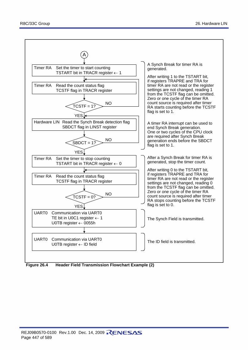
R8C/33C Group 26. Hardware LIN
REJ09B0570-0100 Rev.1.00 Dec. 14, 2009Page 447 of 589
Figure 26.4 Header Field Transmission Flowchart Example (2)
Timer RA Set the timer to start countingTSTART bit in TRACR register ← 1
Timer RA Read the count status flagTCSTF flag in TRACR register
Hardware LIN Read the Synch Break detection flagSBDCT flag in LINST register
Timer RA Set the timer to stop countingTSTART bit in TRACR register ← 0
Timer RA Read the count status flagTCSTF flag in TRACR register
UART0 Communication via UART0TE bit in U0C1 register ← 1U0TB register ← 0055h
A timer RA interrupt can be used toend Synch Break generation.One or two cycles of the CPU clockare required after Synch Breakgeneration ends before the SBDCTflag is set to 1.
The ID field is transmitted.
A
TCSTF = 1?
SBDCT = 1?
YES
TCSTF = 0?
YES
UART0 Communication via UART0U0TB register ← ID field
NO
YES
NO
NO
After writing 0 to the TSTART bit,if registers TRAPRE and TRA fortimer RA are not read or the registersettings are not changed, reading 0from the TCSTF flag can be omitted.Zero or one cycle of the timer RAcount source is required after timerRA stops counting before the TCSTFflag is set to 0.
The Synch Field is transmitted.
After a Synch Break for timer RA isgenerated, stop the timer count.
After writing 1 to the TSTART bit,if registers TRAPRE and TRA fortimer RA are not read or the registersettings are not changed, reading 1from the TCSTF flag can be omitted.Zero or one cycle of the timer RAcount source is required after timerRA starts counting before the TCSTFflag is set to 1.
A Synch Break for timer RA isgenerated.

R8C/33C Group 26. Hardware LIN
REJ09B0570-0100 Rev.1.00 Dec. 14, 2009Page 448 of 589
26.4.2 Slave ModeFigure 26.5 shows an Operating Example during Header Field Reception in slave mode. Figure 26.6 throughFigure 26.8 show examples of Header Field Reception Flowchart.During header field reception, the hardware LIN operates as follows:
(1) When 1 is written to the LSTART bit in the LINCR register for the hardware LIN, Synch Break detection isenabled.
(2) If a “L” level is input for a duration equal to or longer than the period set in timer RA, the hardware LINdetected it as a Synch Break. At this time, the SBDCT flag in the LINST register is set to 1. If the SBIE bitin the LINCR register is set to 1, a timer RA interrupt is generated. Then the hardware LIN enters the SynchField measurement.
(3) The hardware LINA receives a Synch Field (55h) and measures the period of the start bit and bits 0 to 6 isusing timer RA. At this time, whether to input the Synch Field signal to RXD0 of UART0 can be selectedby the SBE bit in the LINCR register.
(4) When the Synch Field measurement is completed, the SFDCT flag in the LINST register is set to 1. If theSFIE bit in the LINCR register is set to 1, a timer RA interrupt is generated.
(5) After the Synch Field measurement is completed, a transfer rate is calculated from the timer RA countvalue. The rate is set in UART0 and registers TRAPRE and TRA for timer RA are set again. Then thehardware LIN receives an ID field via UART0.
(6) After the hardware LIN completes receiving the ID field, it performs communication for a response field.
Figure 26.5 Operating Example during Header Field Reception
RXD0 pin
Synch Break
RXD0 inputfor UART0
RXDSF flag inLINCR register
Synch Field IDENTIFIER
(2) (3) (5) (6)
The above applies when:LINE = 1, MST = 0, SBE = 1, SBIE = 1, SFIE = 1
(4)(1)
SBDCT flag inLINST register
SFDCT flag inLINST register
IR bit inTRAIC register
1 is written to B0CLR bitin LINST register.
This period is measured.
1 is written to B1CLR bitin LINST register.
Set to 0 when an interrupt request is acknowledgedor by a program.
1 is written to LSTART bitin LINCR register. The flag is set to 0 after Synch Field
measurement is completed.

R8C/33C Group 26. Hardware LIN
REJ09B0570-0100 Rev.1.00 Dec. 14, 2009Page 449 of 589
Figure 26.6 Header Field Reception Flowchart Example (1)
Set the count source and registersTRA and TRAPRE as appropriatefor the Synch Break period.
Select the timing at which tounmask the RXD0 input for UART0.If the RXD0 input is chosen to beunmasked after Synch Breakdetection, the Synch Field signal isalso input to UART0.
A
Set the TIOSEL bit in theTRAIOC register to 1 to select thehardware LIN function.If the wake-up function is notnecessary, the setting of the INT1pin can be omitted.
Timer RA Set to pulse width measurement modeBits TMOD2 to TMOD0 in TRAMR register ← 011b
Timer RA Set the pulse width measurement level to lowTEDGSEL bit in TRAIOC register ← 0
Timer RA TRAIO pin assigned to P1_5Bits TRAIOSEL1 to TRAIOSEL0 in TRASR register ← 10b
UART0 RXD0 pin assigned to P1_5RXD0SEL0 bit in U0SR register ← 1
INT1 INT1 pin assigned to P1_5Bits INT1SEL2 to INT1SEL0 in INTSR register ← 001b
Timer RA Set the count source (f1, f2, f8, fOCO)Bits TCK0 to TCK2 in TRAMR register
Timer RA Set the Synch Break widthTRAPRE registerTRA register
Hardware LIN Set the LIN operation to stopLINE bit in LINCR register ← 0
Hardware LIN Set to slave modeMST bit in LINCR register ← 0
Hardware LIN Set the RXD0 input unmasking timing(After Synch Break detection, or after Synch Fieldmeasurement)SBE bit in LINCR register
Hardware LIN Set interrupts to enable(Bus collision detection, Synch Break detection, SynchField measurement)
Bits BCIE, SBIE, SFIE in LINCR register
Hardware LIN Set the LIN operation to startLINE bit in LINCR register ← 1
Notes:1. When the previous communication completes normally and header field reception is
performed again with the same settings, the above settings can be omitted.2. Although the timer-associated registers (TRAMR and TRAIOC) are set before the
TRASR register is set, there is no problem with this flow for the hardware LIN.
(1, 2)
(1)
(1)
(1)
(1)
(1)
(1)
(1, 2)
(1, 2)

R8C/33C Group 26. Hardware LIN
REJ09B0570-0100 Rev.1.00 Dec. 14, 2009Page 450 of 589
Figure 26.7 Header Field Reception Flowchart Example (2)
Timer RA Set pulse width measurement to startTSTART bit in TRACR register ← 1
Timer RA Read the count status flagTCSTF flag in TRACR register
Hardware LIN Set Synch Break detection to startLSTART bit in LINCR register ← 1
Hardware LIN Read the RXD0 input status flagRXDSF flag in LINCR register
A
TCSTF = 1?
YES
RXDSF = 1?
YES
NO
NO
Wait until timer RA starts counting.
Hardware LIN Clear the status flags(Bus collision detection, Synch Breakdetection, Synch Field measurement)Bits B2CLR, B1CLR, B0CLR in LINSTregister ← 1
Hardware LIN Read the Synch Break detection flagSBDCT flag in LINST register
SBDCT = 1?
YES
NO
B
After writing 1 to the LSTART bit,do not apply a “L” level to the RXD0 pinuntil 1 is read from the RXDSF flag.Otherwise, the signal applied during thistime will be input directly to UART0.One or two cycles of the CPU clock andzero or one cycle of the timer RA countsource are required after the LSTART bitis set to 1 before the RXDSF flag is setto 1. After this, input to timer RA andUART0 is enabled.A Synch Break for the hardware LIN isdetected.A timer RA interrupt can be used.
Wait until the RXD0 input to UART0 forthe hardware LIN is masked.
When a Synch Break is detected, timerRA is reloaded with the initially set countvalue.Even if the duration of the input “L” levelis shorter than the set period, timer RA isreloaded with the initially set count value.Wait until the next “L” level is input.One or two cycles of the CPU clock arerequired after Synch Break detectionbefore the SBDCT flag isset to 1.If the SBE bit in the LINCR register is setto 0 (unmasked after Synch Breakdetected), timer RA can be used in timermode after the SBDCT flag in the LINSTregister is set to 1 and the RXDSF flag isset to 0.
Zero or one cycle of the timer RA countsource is required after timer RA startscounting before the TCSTF flag is setto 1.

R8C/33C Group 26. Hardware LIN
REJ09B0570-0100 Rev.1.00 Dec. 14, 2009Page 451 of 589
Figure 26.8 Header Field Reception Flowchart Example (3)
Hardware LIN Read the Synch Field measurement-completed flagSFDCT flag in LINST register
UART0 Set the UART0 communication rateU0BRG register
Communication is performed viaUART0.(The SBDCT flag is set whenthe timer RA counter underflows.)
B
SFDCT = 1?
YES
UART0 Communication via UART0Clock asynchronous serial interface
(UART) mode ID field reception
NO
A Synch Field for the hardware LINis measured.A timer RA interrupt can be used.(The SBDCT flag is set whenthe timer RA counter underflows.)If the SBE bit in the LINCR registeris set to 1 (unmasked after SynchField measurement completed),timer RA can be used in timer modeafter the SFDCT flag in the LINSTregister is set to 1 and the RXDSFflag is set to 0.
Set a communication rate based onthe Synch Field measurementresult.Timer RA Set the Synch Break width again
TRAPRE registerTRA register

R8C/33C Group 26. Hardware LIN
REJ09B0570-0100 Rev.1.00 Dec. 14, 2009Page 452 of 589
26.4.3 Bus Collision Detection FunctionThe bus collision detection function can be used if UART0 is enabled for transmission (TE bit in U0C1 register= 1). To detect a bus collision during Synch Break transmission, set the BCE bit in the LINCR2 register to 1(bus collision detection enabled).Figure 26.9 shows an Operating Example When Bus Collision is Detected.
Figure 26.9 Operating Example When Bus Collision is Detected
TXD0 pin
RXD0 pin
Transfer clock
LINE bit in LINCR register
TE bit inU0C1 register
BCDCT flag inLINST register
IR bit inTRAIC register
Set to 0 when an interrupt request is acknowledgedor by a program.
1 is written to B2CLR bit in LINST register.
Set to 1 by a program.
Set to 1 by a program.

R8C/33C Group 26. Hardware LIN
REJ09B0570-0100 Rev.1.00 Dec. 14, 2009Page 453 of 589
26.4.4 Hardware LIN End ProcessingFigure 26.10 shows an Example of Hardware LIN Communication Completion Flowchart.Use the following timing for hardware LIN end processing:• If the hardware bus collision detection function is used
Perform hardware LIN end processing after checksum transmission completes.• If the bus collision detection function is not used
Perform hardware LIN end processing after header field transmission and reception complete.
Figure 26.10 Example of Hardware LIN Communication Completion Flowchart
Hardware LIN Clear the status flags(Bus collision detection, Synch Break detection, SynchField measurement)Bits B2CLR, B1CLR, B0CLR in LINST register ← 1
Timer RA Read the count status flagTCSTF flag in TRACR register
UART0 Transmission completes via UART0If the bus collision detectionfunction is not used, UART0transmission completionprocessing is not required.
TCSTF = 0?
YES
NO
Set the timer to stop counting.
Zero or one cycle of the timer RAcount source is required aftertimer RA stops counting beforethe TCSTF flag is set to 1.
After clearing the hardware LINstatus flag, stop the hardwareLIN operation.
Timer RA Set the timer to stop countingTSTART bit in TRACR register ← 0
Hardware LIN Set the LIN operation to stopLINE bit in LINCR register ← 0

R8C/33C Group 26. Hardware LIN
REJ09B0570-0100 Rev.1.00 Dec. 14, 2009Page 454 of 589
26.5 Interrupt RequestsThere are four interrupt requests generated by the hardware LIN: Synch Break detection, Completion of SynchBreak generation, Completion of Synch Field measurement, and bus collision detection. These interrupts areshared with timer RA.Table 26.2 lists the Hardware LIN Interrupt Requests.
Table 26.2 Hardware LIN Interrupt Requests
Interrupt Request Status Flag Interrupt Source
Synch Break detection SBDCT Generated when timer RA underflows after the “L” level duration for the RXD0 input is measured, or when a “L” level is input for a duration longer than the Synch Break period during communication.
Completion of Synch Break generation
Generated when a “L” level output to TXD0 for the duration set by timer RA is completed.
Completion of Synch Field measurement
SFDCT Generated when measurement for 6 bits of the Lynch Field by timer RA is completed.
Bus collision detection BCDCT Generated when the RXD0 input and TXD0 output values are different at data latch timing while UART0 is enabled for transmission.

R8C/33C Group 26. Hardware LIN
REJ09B0570-0100 Rev.1.00 Dec. 14, 2009Page 455 of 589
26.6 Notes on Hardware LINFor the time-out processing of the header and response fields, use another timer to measure the duration of timewith a Synch Break detection interrupt as the starting point.

R8C/33C Group 27. A/D Converter
REJ09B0570-0100 Rev.1.00 Dec. 14, 2009Page 456 of 589
27. A/D ConverterThe A/D converter consists of one 10-bit successive approximation A/D converter circuit with a capacitive couplingamplifier. The analog input shares pins P0_0 to P0_7, and P1_0 to P1_3.
27.1 OverviewTable 27.1 lists the A/D Converter Performance. Figure 27.1 shows a Block Diagram of A/D Converter.
Notes:1. When the analog input voltage is over the reference voltage, the A/D conversion result will be 3FFh
in 10-bit mode and FFh in 8-bit mode.2. Refer to Table 32.3 A/D Converter Characteristics for the operating clock φA/D.3. The conversion rate per pin is minimum 43 φAD cycles for 8-bit and 10-bit resolution.
Table 27.1 A/D Converter PerformanceItem Performance
A/D conversion method Successive approximation (with capacitive coupling amplifier)Analog input voltage (1) 0 V to AVCCOperating clock φAD (2) fAD, fAD divided by 2, fAD divided by 4, fAD divided by 8
(fAD=f1 or fOCO-F)Resolution 8 bits or 10 bits selectableAbsolute accuracy AVCC = Vref = 5 V, φAD = 20 MHz
• 8-bit resolution ±2 LSB• 10-bit resolution ±3 LSB
AVCC = Vref = 3.3 V, φAD = 16 MHz• 8-bit resolution ±2 LSB• 10-bit resolution ±5 LSB
AVCC = Vref = 3.0 V, φAD = 10 MHz• 8-bit resolution ±2 LSB• 10-bit resolution ±5 LSB
AVCC = Vref = 2.2 V, φAD = 5 MHz• 8-bit resolution ±2 LSB• 10-bit resolution ±5 LSB
Operating mode One-shot mode, repeat mode 0, repeat mode 1, single sweep mode, and repeat sweep mode
Analog input pin 12 pins (AN0 to AN11)A/D conversion start condition • Software trigger
• Timer RC• External trigger
(Refer to 27.3.3 A/D Conversion Start Condition.)Conversion rate per pin(φAD = fAD) (3)
Minimum 43 φAD cycles

R8C/33C Group 27. A/D Converter
REJ09B0570-0100 Rev.1.00 Dec. 14, 2009Page 457 of 589
Figure 27.1 Block Diagram of A/D Converter
VREFAnalog circuitADSTBY = 0
AVSS
Successive conversionregister
CH2 to CH0
Decoder
Vref
Vin
P1_0/AN8P1_1/AN9
P1_2/AN10P1_3/AN11
CKS0 to CKS2, ADCAP0 to ADCAP1: Bits in ADMOD registerCH0 to CH2, SCAN0 to SCAN1, ADGSEL0 to ADGSEL1: Bits in ADINSEL registerADEX0, ADSTBY, ADDDAEN, ADDDAEL: Bits in ADCON1 registerOCVREFAN: Bit in OCVREFCR register
Software triggerDo not set.
ADCAP1 to ADCAP0
Trigger
P0_7/AN0P0_6/AN1P0_5/AN2P0_4/AN3P0_3/AN4P0_2/AN5P0_1/AN6P0_0/AN7
CKS2 = 0
fOCO-F
f1
CKS2 = 1
AD0 register
ADGSEL1 to ADGSEL0
ADEX0 = 0
SCAN1 to SCAN0
Data bus
Comparator
CH2 to CH0 = 000bCH2 to CH0 = 001bCH2 to CH0 = 010bCH2 to CH0 = 011b
CH2 to CH0 = 000bCH2 to CH0 = 001bCH2 to CH0 = 010bCH2 to CH0 = 011bCH2 to CH0 = 100bCH2 to CH0 = 101bCH2 to CH0 = 110bCH2 to CH0 = 111b
1/2fAD
1/2 1/2
CKS1 to CKS0= 00b
φAD= 01b= 10b= 11b
ADSTBY = 1
AD1 registerAD2 registerAD3 registerAD4 registerAD5 registerAD6 register
= 00b
= 01b
= 10b
= 11bTimer RC triggerADTRG
ADGSEL1 to ADGSEL0
= 00b
= 01b
= 11b
ADEX0 = 1OCVREFAN = 0
OCVREFAN = 1On-chip reference voltage
(OCVREF)
AD7 register
Note:1. When on-chip reference voltage is used as analog input, first set the ADEX0
bit to 1 (on-chip reference voltage selected) and then set the OCVREFAN bit to1 (on-chip reference voltage and analog input are connected).When on-chip reference voltage is not used as analog input, first set theOCVREFAN bit to 0 (on-chip reference voltage and analog input are cut off)and then set the ADEX0 bit to 0 (extended analog input pin not selected).
(Note 1)
ADDDAEN=0ADDDAEN=1
ADDDAEL

R8C/33C Group 27. A/D Converter
REJ09B0570-0100 Rev.1.00 Dec. 14, 2009Page 458 of 589
27.2 Registers
27.2.1 On-Chip Reference Voltage Control Register (OCVREFCR)
Note:1. When on-chip reference voltage is used as analog input, first set the ADEX0 bit in the ADCON1 register to 1 (on-
chip reference voltage selected) and then set the OCVREFAN bit to 1 (on-chip reference voltage and analoginput are connected).When on-chip reference voltage is not used as analog input, first set the OCVREFAN bit to 0 (on-chip referencevoltage and analog input are cut off) and then set the ADEX0 bit to 0 (extended analog input pin not selected).
Set the PRC3 bit in the PRCR register to 1 (write enabled) before rewriting the OCVREFCR register.If the contents of the OCVREFCR register are rewritten during A/D conversion, the conversion result isundefined.
Address 0026hBit b7 b6 b5 b4 b3 b2 b1 b0
Symbol — — — — — — — OCVREFANAfter Reset 0 0 0 0 0 0 0 0
Bit Symbol Bit Name Function R/Wb0 OCVREFAN On-chip reference voltage to
analog input connect bit (1)0: On-chip reference voltage and analog input are cut off1: On-chip reference voltage and analog input are
connected
R/W
b1 — Reserved bits Set to 0. R/Wb2 —b3 —b4 —b5 —b6 —b7 —

R8C/33C Group 27. A/D Converter
REJ09B0570-0100 Rev.1.00 Dec. 14, 2009Page 459 of 589
27.2.2 A/D Register i (ADi) (i = 0 to 7)
If the contents of the ADCON1, ADMOD, ADINSEL, or OCVREFCR register are written during A/Dconversion, the conversion result is undefined.When using the A/D converter in 10-bit mode, repeat mode 0, repeat mode 1, or repeat sweep mode, access theADi register in 16-bit units. Do not access it in 8-bit units.
Address 00C1h to 00C0h (AD0), 00C3h to 00C2h (AD1), 00C5h to 00C4h (AD2),00C7h to 00C6h (AD3), 00C9h to 00C8h (AD4), 00CBh to 00CAh (AD5),00CDh to 00CCh (AD6), 00CFh to 00CEh (AD7)
Bit b7 b6 b5 b4 b3 b2 b1 b0Symbol — — — — — — — —
After Reset X X X X X X X X
Bit b15 b14 b13 b12 b11 b10 b9 b8Symbol — — — — — — — —
After Reset 0 0 0 0 0 0 X X
BitFunction
R/W10-Bit Mode(BITS Bit in ADCON1 Register = 1)
8-Bit Mode(BITS Bit in ADCON1 Register = 0)
b0 8 low-order bits in A/D conversion result A/D conversion result Rb1b2b3b4b5b6b7b8 2 high-order bits in A/D conversion result When read, the content is 0. Rb9
b10 Nothing is assigned. If necessary, set to 0. When read, the content is 0. —b11b12b13b14b15 Reserved bit When read, the content is undefined. R

R8C/33C Group 27. A/D Converter
REJ09B0570-0100 Rev.1.00 Dec. 14, 2009Page 460 of 589
27.2.3 A/D Mode Register (ADMOD)
Note:1. When the CKS2 bit is changed, wait for 3 φAD cycles or more before starting A/D conversion.
If the ADMOD register is rewritten during A/D conversion, the conversion result is undefined.
Address 00D4hBit b7 b6 b5 b4 b3 b2 b1 b0
Symbol ADCAP1 ADCAP0 MD2 MD1 MD0 CKS2 CKS1 CKS0After Reset 0 0 0 0 0 0 0 0
Bit Symbol Bit Name Function R/Wb0 CKS0 Division select bit b1 b0
0 0: fAD divided by 8 0 1: fAD divided by 4 1 0: fAD divided by 2 1 1: fAD divided by 1 (no division)
R/Wb1 CKS1 R/W
b2 CKS2 Clock source select bit (1) 0: Selects f11: Selects fOCO-F
R/W
b3 MD0 A/D operating mode select bit b5 b4 b3 0 0 0: One-shot mode 0 0 1: Do not set. 0 1 0: Repeat mode 0 0 1 1: Repeat mode 1 1 0 0: Single sweep mode 1 0 1: Do not set. 1 1 0: Repeat sweep mode 1 1 1: Do not set.
R/Wb4 MD1 R/Wb5 MD2 R/W
b6 ADCAP0 A/D conversion trigger select bit
b7 b6 0 0: A/D conversion starts by software trigger (ADST bit in
ADCON0 register) 0 1: Do not set. 1 0: A/D conversion starts by conversion trigger from timer
RC 1 1: A/D conversion starts by external trigger (ADTRG)
R/Wb7 ADCAP1 R/W

R8C/33C Group 27. A/D Converter
REJ09B0570-0100 Rev.1.00 Dec. 14, 2009Page 461 of 589
27.2.4 A/D Input Select Register (ADINSEL)
If the ADINSEL register is rewritten during A/D conversion, the conversion result is undefined.
Address 00D5hBit b7 b6 b5 b4 b3 b2 b1 b0
Symbol ADGSEL1 ADGSEL0 SCAN1 SCAN0 — CH2 CH1 CH0After Reset 1 1 0 0 0 0 0 0
Bit Symbol Bit Name Function R/Wb0 CH0 Analog input pin select bit Refer to Table 27.2 Analog Input Pin Selection R/Wb1 CH1 R/Wb2 CH2 R/Wb3 — Reserved bit Set to 0. R/Wb4 SCAN0 A/D sweep pin count select bit b5 b4
0 0: 2 pins 0 1: 4 pins 1 0: 6 pins 1 1: 8 pins
R/Wb5 SCAN1 R/W
b6 ADGSEL0 A/D input group select bit b7 b6 0 0: Port P0 group selected 0 1: Port P1 group selected 1 0: Do not set. 1 1: Port group not selected
R/Wb7 ADGSEL1 R/W
Table 27.2 Analog Input Pin SelectionBits CH2 to CH0 Bits ADGSEL1, ADGSEL0 = 00b Bits ADGSEL1, ADGSEL0 = 01b
000b AN0 AN8001b AN1 AN9010b AN2 AN10011b AN3 AN11100b AN4 Do not set.101b AN5110b AN6111b AN7
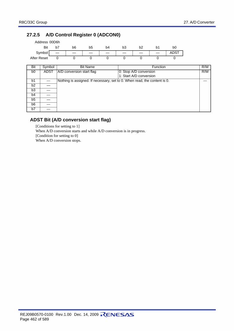
R8C/33C Group 27. A/D Converter
REJ09B0570-0100 Rev.1.00 Dec. 14, 2009Page 462 of 589
27.2.5 A/D Control Register 0 (ADCON0)
ADST Bit (A/D conversion start flag)[Conditions for setting to 1]When A/D conversion starts and while A/D conversion is in progress.[Condition for setting to 0]When A/D conversion stops.
Address 00D6hBit b7 b6 b5 b4 b3 b2 b1 b0
Symbol — — — — — — — ADSTAfter Reset 0 0 0 0 0 0 0 0
Bit Symbol Bit Name Function R/Wb0 ADST A/D conversion start flag 0: Stop A/D conversion
1: Start A/D conversionR/W
b1 — Nothing is assigned. If necessary, set to 0. When read, the content is 0. —b2 —b3 —b4 —b5 —b6 —b7 —

R8C/33C Group 27. A/D Converter
REJ09B0570-0100 Rev.1.00 Dec. 14, 2009Page 463 of 589
27.2.6 A/D Control Register 1 (ADCON1)
Notes:1. When on-chip reference voltage is used as analog input, first set the ADEX0 bit to 1 (on-chip reference voltage
selected) and then set the OCVREFAN bit in the OCVREFCR register to 1 (on-chip reference voltage and analoginput are connected).When on-chip reference voltage is not used as analog input, first set the OCVREFAN bit to 0 (on-chip referencevoltage and analog input are cut off) and then set the ADEX0 bit to 0 (extended analog input pin not selected).
2. Do not set to 1 (A/D conversion using comparison reference voltage as input) in single sweep mode or repeatsweep mode.
3. When the ADSTBY bit is changed from 0 (A/D operation stops) to 1 (A/D operation enabled), wait for 1 φAD cycleor more before starting A/D conversion.
4. To enable the A/D open-circuit detection assist function, select the conversion start state with the ADDDAEL bitafter setting the ADDDAEN bit to 1 (enabled).The conversion result with an open circuit varies with external circuits. Careful evaluation should be performedaccording to the system before using this function.
If the ADCON1 register is rewritten during A/D conversion, the conversion result is undefined.
Address 00D7hBit b7 b6 b5 b4 b3 b2 b1 b0
Symbol ADDDAEL ADDDAEN ADSTBY BITS — — — ADEX0After Reset 0 0 0 0 0 0 0 0
Bit Symbol Bit Name Function R/Wb0 ADEX0 Extended analog input pin select bit (1) 0: Extended analog input pin not selected
1: On-chip reference voltage selected (2)R/W
b1 — Reserved bits Set to 0. R/Wb2 —b3 —b4 BITS 8/10-bit mode select bit 0: 8-bit mode
1: 10-bit modeR/W
b5 ADSTBY A/D standby bit (3) 0: A/D operation stops (standby)1: A/D operation enabled
R/W
b6 ADDDAEN A/D open-circuit detection assist function enable bit (4)
0: Disabled1: Enabled
R/W
b7 ADDDAEL A/D open-circuit detection assist method select bit (4)
0: Discharge before conversion1: Precharge before conversion
R/W

R8C/33C Group 27. A/D Converter
REJ09B0570-0100 Rev.1.00 Dec. 14, 2009Page 464 of 589
27.3 Common Items for Multiple Modes
27.3.1 Input/Output PinsThe analog input shares pins P0_0 to P0_7, and P1_0 to P1_3 in AN0 to AN11.When using the ANi (i = 0 to 11) pin as input, set the corresponding port direction bit to 0 (input mode).After changing the A/D operating mode, select an analog input pin again.
27.3.2 A/D Conversion CyclesFigure 27.2 shows a Timing Diagram of A/D Conversion. Figure 27.3 shows the A/D Conversion Cycles (φAD= fAD).
Figure 27.2 Timing Diagram of A/D Conversion
Figure 27.3 A/D Conversion Cycles (φAD = fAD)
A/D conversion execution time
Sampling time15 φAD cycles
Conversion time of 1st bit 2nd bit
Comparisontime
Comparisontime ……
* Repeat until conversion ends
Comparisontime
Open-circuitdetection
Charging time
Comparisontime End process
Open-circuitdetection End process
Startprocess
Start process
Conversion time(Minimum) (1)
43 φAD 1 φAD
Open-circuitdetection
Charging time
ComparisontimeSampling time
End processConversion time at the 1st bit
Comparisontime
Conversion timeat the 2nd bit and
the follows
Disabled: 0 φAD
Start process(Minimum)
Enabled: 2 φAD
End process
Open-circuitdetection
15 φAD 2.5 φAD 2.5 φAD 2 φAD
Note:1. The conversion time (minimum) is 43 φAD for 8-bit and 10-bit resolution.
A/D conversion execution time
Start process
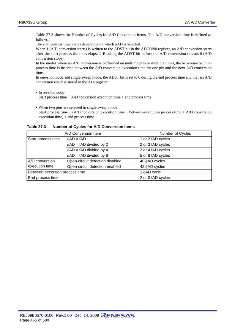
R8C/33C Group 27. A/D Converter
REJ09B0570-0100 Rev.1.00 Dec. 14, 2009Page 465 of 589
Table 27.3 shows the Number of Cycles for A/D Conversion Items. The A/D conversion time is defined asfollows.The start process time varies depending on which φAD is selected.When 1 (A/D conversion starts) is written to the ADST bit in the ADCON0 register, an A/D conversion startsafter the start process time has elapsed. Reading the ADST bit before the A/D conversion returns 0 (A/Dconversion stops).In the modes where an A/D conversion is performed on multiple pins or multiple times, the between-executionprocess time is inserted between the A/D conversion execution time for one pin and the next A/D conversiontime. In one-shot mode and single sweep mode, the ADST bit is set to 0 during the end process time and the last A/Dconversion result is stored in the ADi register.
• In on-shot modeStart process time + A/D conversion execution time + end process time
• When two pins are selected in single sweep modeStart process time + (A/D conversion execution time + between-execution process time + A/D conversionexecution time) + end process time
Table 27.3 Number of Cycles for A/D Conversion ItemsA/D Conversion Item Number of Cycles
Start process time φAD = fAD 1 or 2 fAD cyclesφAD = fAD divided by 2 2 or 3 fAD cyclesφAD = fAD divided by 4 3 or 4 fAD cyclesφAD = fAD divided by 8 5 or 6 fAD cycles
A/D conversion execution time
Open-circuit detection disabled 40 φAD cyclesOpen-circuit detection enabled 42 φAD cycles
Between-execution process time 1 φAD cycleEnd process time 2 or 3 fAD cycles

R8C/33C Group 27. A/D Converter
REJ09B0570-0100 Rev.1.00 Dec. 14, 2009Page 466 of 589
27.3.3 A/D Conversion Start ConditionA software trigger, trigger from timer RC, and external trigger are used as A/D conversion start triggers. Figure 27.4 shows the Block Diagram of A/D Conversion Start Control Unit.
Figure 27.4 Block Diagram of A/D Conversion Start Control Unit
27.3.3.1 Software TriggerA software trigger is selected when bits ADCAP1 to ADCAP0 in the ADMOD register are set to 00b (softwaretrigger).The A/D conversion starts when the ADST bit in the ADCON0 register is set to 1 (A/D conversion starts).
27.3.3.2 Trigger from Timer RCThis trigger is selected when bits ADCAP1 to ADCAP0 in the ADMOD register are set to 10b (timer RC).To use this function, make sure the following conditions are met.
• Bits ADCAP1 to ADCAP0 in the ADMOD register are set to 10b (timer RC).• Timer RC is used in the output compare function (timer mode, PWM mode, PWM2 mode).• The ADTRGjE bit (j = A, B, C, D) in the TRCADCR register is set to 1 (A/D trigger occurs at compare match
with TRCGRj register).• The ADST bit in the ADCON0 register is set to 1 (A/D conversion starts).
When the IMFj bit in the TRCSR register is changed from 0 to 1, A/D conversion starts. Refer to 19. Timer RC, 19.5 Timer Mode (Output Compare Function), 19.6 PWM Mode, 19.7 PWM2Mode for the details of timer RC and the output compare function (timer mode, PWM mode, and PWM2mode).
j = A, B, C, D k = 0 to 1
ADCAP1 to ADCAP0: Bits in ADMOD registerADST: Bit in ADCON0 registerADTRGjE: Bit in TRCADCR registerINT0EN: Bit in INTEN registerIMFj: Bit in TRCSR registerPD4_5: Bit in PD4 register
ADSTA/D conversion start trigger
ADCAP1 to ADCAP0 (1)
= 00b= 10b
= 11b
INT0EN
IMFj(TRCSR register) ADTRGjE
ADTRG pinPD4_5
Note:1. Do not set bits ADCAP1 to ADCAP0 to 01b.

R8C/33C Group 27. A/D Converter
REJ09B0570-0100 Rev.1.00 Dec. 14, 2009Page 467 of 589
27.3.3.3 External TriggerThis trigger is selected when bits ADCAP1 to ADCAP0 in the ADMOD register are set to 11b (external trigger(ADTRG)).To use this function, make sure the following conditions are met.
• Bits ADCAP1 to ADCAP0 in the ADMOD register are set to 11b (external trigger (ADTRG)).• Set the INT0EN bit in the INTEN register to 1 (INT0 input enabled) and the INT0PL bit to 0 (one edge), and
set the POL bit in the INT0IC register to 0 (falling edge selected).• Set the PD4_5 bit in the PD4 register to 0 (input mode).• Select the INT0 digital filter by bits INT0F1 to INT0F0 in the INTF register.• The ADST bit in the ADCON0 register is set to 1 (A/D conversion starts).
The IR bit in the INT0IC register is set to 1 (interrupt requested) in accordance with the setting of the POL bit inthe INT0IC register and the INT0PL bit in the INTEN register and a change in the ADTRG pin input (refer to11.8 Notes on Interrupts).For details on interrupts, refer to 11. Interrupts.
When the ADTRG pin input is changed from “H” to “L” under the above conditions, A/D conversion starts.

R8C/33C Group 27. A/D Converter
REJ09B0570-0100 Rev.1.00 Dec. 14, 2009Page 468 of 589
27.3.4 A/D Conversion ResultThe A/D conversion result is stored in the ADi register (i = 0 to 7). The register where the result is stored variesdepending on the A/D operating mode used. The contents of the ADi register are undefined after a reset. Valuescannot be written to the ADi register.
In repeat mode 0, no interrupt request is generated. After the first AD conversion is completed, determine if theA/D conversion time has elapsed by a program.In one-shot mode, repeat mode 1, single sweep mode, and repeat sweep mode, an interrupt request is generatedat certain times, such as when an A/D conversion completes (the IR bit in the ADIC register is set to 1). However, in repeat mode 1 and repeat sweep mode, A/D conversion continues after an interrupt request isgenerated. Read the ADi register before the next A/D conversion is completed, since at completion the ADiregister is rewritten with the new value.
In one-shot mode and single sweep mode, when bits ADCAP1 to ADCAP0 in the ADMOD register is set to00b (software trigger), the ADST bit in the ADCON0 register is used to determine whether the A/D conversionor sweep has completed.
During an A/D conversion operation, if the ADST bit in the ADCON0 register is set to 0 (A/D conversionstops) by a program to forcibly terminate A/D conversion, the conversion result of the A/D converter isundefined and no interrupt is generated. The value of the ADi register before A/D conversion may also beundefined.If the ADST bit is set to 0 by a program, do not use the value of all the ADi register.
27.3.5 Low Current Consumption FunctionWhen the A/D converter is not used, power consumption can be reduced by setting the ADSTBY bit in theADCON1 register to 0 (A/D operation stops (standby)) to shut off any analog circuit current flow. To use the A/D converter, set the ADSTBY bit to 1 (A/D operation enabled) and wait for 1 φAD cycle or morebefore setting the ADST bit in the ADCON0 register to 1 (A/D conversion starts). Do not write 1 to bits ADSTand ADSTBY at the same time. Also, do not set the ADSTBY bit to 0 (A/D operation stops (standby)) during A/D conversion.
27.3.6 Extended Analog Input PinsIn one-shot mode, repeat mode 0, and repeat mode 1, the on-chip reference voltage (OCVREF) can be used asanalog input.Any variation in VREF can be confirmed using the on-chip reference voltage. Use the ADEX0 bit in theADCON1 register and the OCVREFAN bit in the OCVREFCR register to select the on-chip reference voltage. The A/D conversion result of the on-chip reference voltage in one-shot mode or in repeat mode 0 is stored in theAD0 register.
27.3.7 A/D Open-Circuit Detection Assist FunctionTo suppress influences of the analog input voltage leakage from the previously converted channel during A/Dconversion operation, a function is incorporated to fix the electric charge on the chopper amp capacitor to thepredetermined state (AVCC or GND) before starting conversion.This function enables more reliable detection of an open circuit in the wiring connected to the analog input pins.Figure 27.5 shows the A/D Open-Circuit Detection Example on AVCC Side (Precharge before ConversionSelected) and Figure 27.6 shows the A/D Open-Circuit Detection Example on AVSS Side (Discharge beforeConversion Selected).

R8C/33C Group 27. A/D Converter
REJ09B0570-0100 Rev.1.00 Dec. 14, 2009Page 469 of 589
Figure 27.5 A/D Open-Circuit Detection Example on AVCC Side (Precharge before Conversion Selected)
Figure 27.6 A/D Open-Circuit Detection Example on AVSS Side (Discharge before Conversion Selected)
External circuitexample (1)
Open
RAnalog input
ANi
ON
Precharge
ADDDAENOFF
Chopper ampcapacitor
i = 0 to 11
Prechargecontrol signal
Dischargecontrol signal
C
Note:1. The conversion result for an open circuit varies with external circuits. Careful evaluation should be
performed before using this function.
External circuitexample (1)
Open R
Analog inputANi
OFF
Discharge
ADDDAENON
Chopper ampcapacitor
i = 0 to 11
Prechargecontrol signal
Dischargecontrol signal
C
Note:1. The conversion result for an open circuit varies with external circuits. Careful evaluation should be
performed before using this function.

R8C/33C Group 27. A/D Converter
REJ09B0570-0100 Rev.1.00 Dec. 14, 2009Page 470 of 589
27.4 One-Shot ModeIn one-shot mode, the input voltage to one pin selected from among AN0 to AN11 or OCVREF is A/D convertedonce.Table 27.4 lists the One-Shot Mode Specifications.
Table 27.4 One-Shot Mode SpecificationsItem Specification
Function The input voltage to the pin selected by bits CH2 to CH0 and bits ADGSEL1 to ADGSEL0 in the ADINSEL register or the ADEX0 bit in the ADCON1 register is A/D converted once.
Resolution 8 bits or 10 bitsA/D conversion start condition • Software trigger
• Timer RC• External trigger
(Refer to 27.3.3 A/D Conversion Start Condition)A/D conversion stop condition • A/D conversion completes (If bits ADCAP1 to ADCAP0 in the
ADMOD register are set to 00b (software trigger), the ADST bit in the ADCON0 register is set to 0.)
• Set the ADST bit to 0Interrupt request generation timing
When A/D conversion completes
Analog input pin One pin selectable from among AN0 to AN11, or OCVREF.Storage resister for A/D conversion result
AD0 register: AN0, AN8, OCVREFAD1 register: AN1, AN9AD2 register: AN2, AN10AD3 register: AN3, AN11AD4 register: AN4AD5 register: AN5AD6 register: AN6AD7 register: AN7
Reading of result of A/D converter
Read register AD0 to AD7 corresponding to the selected pin.

R8C/33C Group 27. A/D Converter
REJ09B0570-0100 Rev.1.00 Dec. 14, 2009Page 471 of 589
27.5 Repeat Mode 0In repeat mode 0, the input voltage to one pin selected from among AN0 to AN11 or OCVREF is A/D convertedrepeatedly.Table 27.5 lists the Repeat Mode 0 Specifications.
Table 27.5 Repeat Mode 0 SpecificationsItem Specification
Function The input voltage to the pin selected by bits CH2 to CH0 and bits ADGSEL1 to ADGSEL0 in the ADINSEL register or the ADEX0 bit in the ADCON1 register is A/D converted repeatedly.
Resolution 8 bits or 10 bitsA/D conversion start condition • Software trigger
• Timer RC• External trigger
(Refer to 27.3.3 A/D Conversion Start Condition)A/D conversion stop condition Set the ADST bit in the ADCON0 register to 0Interrupt request generation timing
Not generated
Analog input pin One pin selectable from among AN0 to AN11, or OCVREF.Storage resister for A/D conversion result
AD0 register: AN0, AN8, OCVREFAD1 register: AN1, AN9AD2 register: AN2, AN10AD3 register: AN3, AN11AD4 register: AN4AD5 register: AN5AD6 register: AN6AD7 register: AN7
Reading of result of A/D converter
Read register AD0 to AD7 corresponding to the selected pin.

R8C/33C Group 27. A/D Converter
REJ09B0570-0100 Rev.1.00 Dec. 14, 2009Page 472 of 589
27.6 Repeat Mode 1In repeat mode 1, the input voltage to one pin selected from among AN0 to AN11 or OCVREF is A/D convertedrepeatedly.Table 27.6 lists the Repeat Mode 1 Specifications. Figure 27.7 shows the Operating Example of Repeat Mode 1.
Table 27.6 Repeat Mode 1 SpecificationsItem Specification
Function The input voltage to the pin selected by bits CH2 to CH0 and bits ADGSEL1 to ADGSEL0 in the ADINSEL register or the ADEX0 bit in the ADCON1 register is A/D converted repeatedly.
Resolution 8 bits or 10 bitsA/D conversion start condition • Software trigger
• Timer RC• External trigger
(Refer to 27.3.3 A/D Conversion Start Condition)A/D conversion stop condition Set the ADST bit in the ADCON0 register to 0Interrupt request generation timing
When the A/D conversion result is stored in the AD7 register.
Analog input pin One pin selectable from among AN0 to AN11, or OCVREF.Storage resister for A/D conversion result
AD0 register: 1st A/D conversion result, 9th A/D conversion result...AD1 register: 2nd A/D conversion result, 10th A/D conversion result...AD2 register: 3rd A/D conversion result, 11th A/D conversion result...AD3 register: 4th A/D conversion result, 12th A/D conversion result...AD4 register: 5th A/D conversion result, 13th A/D conversion result...AD5 register: 6th A/D conversion result, 14th A/D conversion result...AD6 register: 7th A/D conversion result, 15th A/D conversion result...AD7 register: 8th A/D conversion result, 16th A/D conversion result...
Reading of result of A/D converter
Read registers AD0 to AD7

R8C/33C Group 27. A/D Converter
REJ09B0570-0100 Rev.1.00 Dec. 14, 2009Page 473 of 589
Figure 27.7 Operating Example of Repeat Mode 1
8th A/D conversion result
7th A/D conversion result
The above applies under the following conditions:Bits ADCAP1 to ADCAP0 in the ADMOD register are set to 00b (starts by software trigger).
Set to 0 when interruptrequest is acknowledged,or set by a program.
Successive conversionregister 1st 2nd 3rd 4th
AD0 register Undefined
ADST bit inADCON0 register
AD1 register Undefined
AD2 register Undefined
AD3 register Undefined
1st A/D conversion result
2nd A/D conversion result
3rd A/D conversion result
4th A/D conversion result
IR bit inADIC register
5th 6th 7th 8th 9th
Undefined
Undefined
Undefined
Undefined
5th A/D conversion result
6th A/D conversion result
AD4 register
AD5 register
AD6 register
AD7 register
9th A/D conversion result

R8C/33C Group 27. A/D Converter
REJ09B0570-0100 Rev.1.00 Dec. 14, 2009Page 474 of 589
27.7 Single Sweep ModeIn single sweep mode, the input voltage to two, four, six, or eight pins selected from among AN0 to AN11 are A/Dconverted once. Table 27.7 lists the Single Sweep Mode Specifications. Figure 27.8 shows the Operating Example of Single SweepMode.
Table 27.7 Single Sweep Mode SpecificationsItem Specification
Function The input voltage to the pins selected by bits ADGSEL1 to ADGSEL0 and bits SCAN1 to SCAN0 in the ADINSEL register is A/D converted once.
Resolution 8 bits or 10 bitsA/D conversion start condition • Software trigger
• Timer RC• External trigger
(Refer to 27.3.3 A/D Conversion Start Condition)A/D conversion stop condition • If two pins are selected, when A/D conversion of the two selected pins
completes (the ADST bit in the ADCON0 register is set to 0).• If four pins are selected, when A/D conversion of the four selected pins
completes (the ADST bit is set to 0).• If six pins are selected, when A/D conversion of the six selected pins
completes (the ADST bit is set to 0).• If eight pins are selected, when A/D conversion of the eight selected
pins completes (the ADST bit is set to 0).• Set the ADST bit to 0.
Interrupt request generation timing
• If two pins are selected, when A/D conversion of the two selected pins completes.
• If four pins are selected, when A/D conversion of the four selected pins completes.
• If six pins are selected, when A/D conversion of the six selected pins completes.
• If eight pins are selected, when A/D conversion of the eight selected pins completes.
Analog input pin AN0 to AN1(2 pins), AN8 to AN9(2 pins), AN0 to AN3(4 pins), AN8 to AN11(4 pins), AN0 to AN5(6 pins), AN0 to AN7(8 pins)(Selectable by bits SCAN1 to SCAN0 and bits ADGSEL1 to ADGSEL0.)
Storage resister for A/D conversion result
AD0 register: AN0, AN8AD1 register: AN1, AN9AD2 register: AN2, AN10AD3 register: AN3, AN11AD4 register: AN4AD5 register: AN5AD6 register: AN6AD7 register: AN7
Reading of result of A/D converter
Read the registers from AD0 to AD7 corresponding to the selected pin.
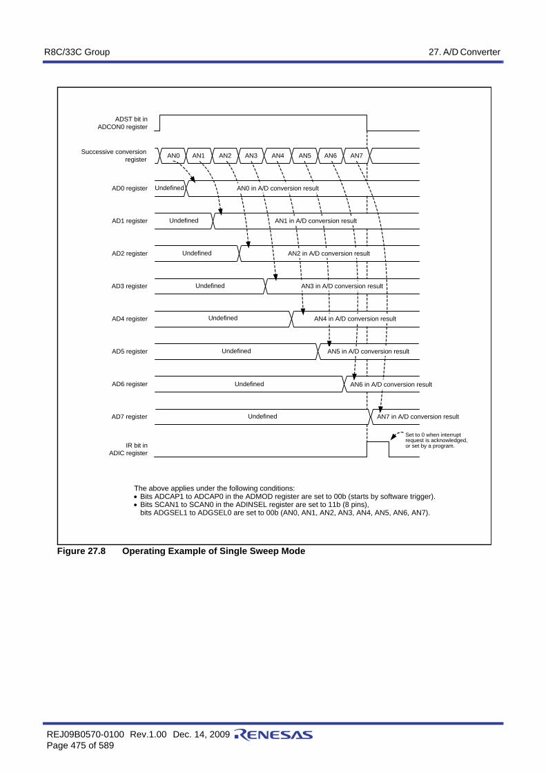
R8C/33C Group 27. A/D Converter
REJ09B0570-0100 Rev.1.00 Dec. 14, 2009Page 475 of 589
Figure 27.8 Operating Example of Single Sweep Mode
AN7 in A/D conversion result
AN6 in A/D conversion result
Set to 0 when interruptrequest is acknowledged,or set by a program.
Successive conversionregister AN0 AN1 AN2 AN3
AD0 register Undefined
ADST bit inADCON0 register
AD1 register Undefined
AD2 register Undefined
AD3 register Undefined
AN0 in A/D conversion result
AN1 in A/D conversion result
AN2 in A/D conversion result
AN3 in A/D conversion result
IR bit inADIC register
AN4 AN5 AN6 AN7
Undefined
Undefined
Undefined
Undefined
AN4 in A/D conversion result
AN5 in A/D conversion result
AD4 register
AD5 register
AD6 register
AD7 register
The above applies under the following conditions:• Bits ADCAP1 to ADCAP0 in the ADMOD register are set to 00b (starts by software trigger).• Bits SCAN1 to SCAN0 in the ADINSEL register are set to 11b (8 pins),
bits ADGSEL1 to ADGSEL0 are set to 00b (AN0, AN1, AN2, AN3, AN4, AN5, AN6, AN7).

R8C/33C Group 27. A/D Converter
REJ09B0570-0100 Rev.1.00 Dec. 14, 2009Page 476 of 589
27.8 Repeat Sweep ModeIn repeat sweep mode, the input voltage to two, four, six, or eight pins selected from among AN0 to AN11 are A/Dconverted repeatedly.Table 27.8 lists the Repeat Sweep Mode Specifications. Figure 27.9 shows the Operating Example of RepeatSweep Mode.
Table 27.8 Repeat Sweep Mode SpecificationsItem Specification
Function The input voltage to the pins selected by bits ADGSEL1 to ADGSEL0 and bits SCAN1 to SCAN0 in the ADINSEL register are A/D converted repeatedly.
Resolution 8 bits or 10 bitsA/D conversion start condition • Software trigger
• Timer RC• External trigger
(Refer to 27.3.3 A/D Conversion Start Condition)A/D conversion stop condition Set the ADST bit in the ADCON0 register to 0Interrupt request generation timing
• If two pins are selected, when A/D conversion of the two selected pins completes.
• If four pins are selected, when A/D conversion of the four selected pins completes.
• If six pins are selected, when A/D conversion of the six selected pins completes.
• If eight pins are selected, when A/D conversion of the eight selected pins completes.
Analog input pin AN0 to AN1(2 pins), AN8 to AN9(2 pins), AN0 to AN3(4 pins), AN8 to AN11(4 pins), AN0 to AN5(6 pins), AN0 to AN7(8 pins)(Selectable by bits SCAN1 to SCAN0 and bits ADGSEL1 to ADGSEL0.)
Storage resister for A/D conversion result
AD0 register: AN0, AN8AD1 register: AN1, AN9AD2 register: AN2, AN10AD3 register: AN3, AN11AD4 register: AN4AD5 register: AN5AD6 register: AN6AD7 register: AN7
Reading of result of A/D converter
Read the registers from AD0 to AD7 corresponding to the selected pin.

R8C/33C Group 27. A/D Converter
REJ09B0570-0100 Rev.1.00 Dec. 14, 2009Page 477 of 589
Figure 27.9 Operating Example of Repeat Sweep Mode
AN7 in A/D conversion result
AN6 in A/D conversion result
Set to 0 when interruptrequest is acknowledged,or set by a program.
Successive conversionregister AN0 AN1 AN2 AN3
AD0 register Undefined
ADST bit inADCON0 register
AD1 register Undefined
AD2 register Undefined
AD3 register Undefined
AN0 in A/D conversion result
AN1 in A/D conversion result
AN2 in A/D conversion result
AN3 in A/D conversion result
IR bit inADIC register
AN4 AN5 AN6 AN7
Undefined
Undefined
Undefined
Undefined
AN4 in A/D conversion result
AN5 in A/D conversion result
AD4 register
AD5 register
AD6 register
AD7 register
The above applies under the following conditions:• Bits ADCAP1 to ADCAP0 in the ADMOD register are set to 00b (starts by software trigger).• Bits SCAN1 to SCAN0 in the ADINSEL register are set to 11b (8 pins),
bits ADGSEL1 to ADGSEL0 are set to 00b (AN0, AN1, AN2, AN3, AN4, AN5, AN6, and AN7).
AN0
AN0 in A/D conversion result

R8C/33C Group 27. A/D Converter
REJ09B0570-0100 Rev.1.00 Dec. 14, 2009Page 478 of 589
27.9 Output Impedance of Sensor under A/D ConversionTo carry out A/D conversion properly, charging the internal capacitor C shown in Figure 27.10 has to be completedwithin a specified period of time. T (sampling time) as the specified time. Let output impedance of sensorequivalent circuit be R0, internal resistance of microcomputer be R, precision (error) of the A/D converter be X,and the resolution of A/D converter be Y (Y is 1024 in the 10-bit mode, and 256 in the 8-bit mode).
VC is generally
And when t = T,
Hence,
Figure 27.10 shows the Analog Input Pin and External Sensor Equivalent Circuit. When the difference betweenVIN and VC becomes 0.1LSB, we find impedance R0 when voltage between pins VC changes from 0 to VIN-(0.1/1024) VIN in time T. (0.1/1024) means that A/D precision drop due to insufficient capacitor charge is held to0.1LSB at time of A/D conversion in the 10-bit mode. Actual error however is the value of absolute precisionadded to 0.1LSB. T = 0.75 µs when φAD = 20 MHz. Output impedance R0 for sufficiently charging capacitor C within time T isdetermined as follows.
T = 0.75 µs, R = 10 kΩ, C = 6.0 pF, X = 0.1, and Y = 1024. Hence,
Thus, the allowable output impedance of the sensor equivalent circuit, making the precision (error) 0.1LSB or less,is approximately 3.5 kΩ. maximum.
Figure 27.10 Analog Input Pin and External Sensor Equivalent Circuit
VC VIN 1 e 1C R0 R+( )--------------------------– t
–
=
1C R0 R+( )--------------------------– T X
Y----ln=
e 1C R0 R+( )--------------------------T– X
Y----=
VC VIN XY---- VIN VIN 1 X
Y----–
=–=
R0 T
C XY----ln•
-------------------– R–=
R0 0.75 10 6–×
6.0 10 12– 0.11024------------ln•×
---------------------------------------------------–= 10 3×10– 3.5 3×10≈
R0 R (10 kΩ)
C (6.0 pF)VIN
VC
MCU
Sensor equivalentcircuit

R8C/33C Group 27. A/D Converter
REJ09B0570-0100 Rev.1.00 Dec. 14, 2009Page 479 of 589
27.10 Notes on A/D Converter• Write to the ADMOD register, the ADINSEL register, the ADCON0 register (other than ADST bit), the
ADCON1 register, the OCVREFCR register when A/D conversion is stopped (before a trigger occurs).• To use the A/D converter in repeat mode 0, repeat mode 1, or repeat sweep mode, select the frequency of the A/D
converter operating clock φAD or more for the CPU clock during A/D conversion. Do not select fOCO-F as φAD.
• Connect 0.1 µF capacitor between the VREF pin and AVSS pin.• Do not enter stop mode during A/D conversion.• Do not enter wait mode during A/D conversion regardless of the state of the CM02 bit in the CM0 register (1:
Peripheral function clock stops in wait mode or 0: Peripheral function clock does not stop in wait mode). • Do not set the FMSTP bit in the FMR0 register to 1 (flash memory stops) or the FMR27 bit to 1 (low-current-
consumption read mode enabled) during A/D conversion. Otherwise, the A/D conversion result will beundefined.
• Do not change the CKS2 bit in the ADMOD register while fOCO-F is stopped.• During an A/D conversion operation, if the ADST bit in the ADCON0 register is set to 0 (A/D conversion stops)
by a program to forcibly terminate A/D conversion, the conversion result of the A/D converter is undefined andno interrupt is generated. The value of the ADi register before A/D conversion may also be undefined. If the ADST bit is set to 0 by a program, do not use the value of all the ADi register.

R8C/33C Group 28. D/A Converter
REJ09B0570-0100 Rev.1.00 Dec. 14, 2009Page 480 of 589
28. D/A ConverterThe D/A converters are 8-bit R-2R type units. There are two independent D/A converters.
28.1 OverviewD/A conversion is performed by writing a value to the DAi register (i = 0 or 1). To output the conversion result, setthe DAiE bit in the DACON register to 1 (output enabled). Before using D/A conversion, set the corresponding bitsPD0_6 and PD0_7 in the PD0 register to 0 (input mode) and the PU01 bit in the PUR0 register to 0 (not pulled up).The output analog voltage (V) is determined by the setting value n (n: decimal) of the DAi register.
V = Vref × n/ 256 (n = 0 to 255)Vref: Reference voltage
Table 28.1 lists the D/A Converter Specifications. Figure 28.1 shows the D/A Converter Block Diagram and Figure28.2 shows the D/A Converter Equivalent Circuit.
Figure 28.1 D/A Converter Block Diagram
Table 28.1 D/A Converter SpecificationsItem Performance
D/A conversion method R-2R methodResolution 8 bitsAnalog output pins 2 (DA0 and DA1)
DA0 register
R-2R resistor ladder
DA0E bit
DA0
DA1 register
R-2R resistor ladder
DA1E bit
DA1
0
1
0
1
Dat
a bu
s

R8C/33C Group 28. D/A Converter
REJ09B0570-0100 Rev.1.00 Dec. 14, 2009Page 481 of 589
Figure 28.2 D/A Converter Equivalent Circuit
VREF
AVSS
2R
R
2R
R
2R
R
2R
R
2R
R
2R
R
2R
R
2R
2R
DAi
MSB LSB
DAiE bit
DAi register
Note:1. The above diagram applies when the value of the DAi register is 2Ah.
R
i = 0 or 1
0
0
1
1

R8C/33C Group 28. D/A Converter
REJ09B0570-0100 Rev.1.00 Dec. 14, 2009Page 482 of 589
28.2 Registers
28.2.1 D/Ai Register (DAi) (i = 0 or 1)
When the D/A converter is not used, set the DAiE bit (i = 0 or 1) to 0 (output disabled) and set the DAi registerto 00h to prevent current from flowing into the R-2R resistor ladder to reduce unnecessary current consumption.
28.2.2 D/A Control Register (DACON)
When the D/A converter is not used, set the DAiE bit (i = 0 or 1) to 0 (output disabled) and set the DAi registerto 00h to prevent current from flowing into the R-2R resistor ladder to reduce unnecessary current consumption.
Address 00D8h (DA0), 00D9h (DA1) Bit b7 b6 b5 b4 b3 b2 b1 b0
Symbol — — — — — — — —After Reset 0 0 0 0 0 0 0 0
Bit Function Setting Range R/Wb7-b0 Output value of D/A conversion 00h to FFh R/W
Address 00DChBit b7 b6 b5 b4 b3 b2 b1 b0
Symbol — — — — — — DA1E DA0EAfter Reset 0 0 0 0 0 0 0 0
Bit Symbol Bit Name Function R/Wb0 DA0E D/A0 output enable bit 0: Output disabled
1: Output enabledR/W
b1 DA1E D/A1 output enable bit 0: Output disabled1: Output enabled
R/W
b2 — Nothing is assigned. If necessary, set to 0. When read, the content is 0. —b3 —b4 —b5 —b6 —b7 —

R8C/33C Group 29. Comparator B
REJ09B0570-0100 Rev.1.00 Dec. 14, 2009Page 483 of 589
29. Comparator BComparator B compares a reference input voltage and an analog input voltage. Comparator B1 and comparator B3 areindependent of each other.
29.1 OverviewThe comparison result of the reference input voltage and analog input voltage can be read by software. An input tothe IVREFi (i = 1 or 3) pin can be used as the reference input voltage.Table 29.1 lists the Comparator B Specifications, Figure 29.1 shows a Comparator B Block Diagram, and Table29.2 lists the I/O Pins.
i = 1 or 3
Figure 29.1 Comparator B Block Diagram
Table 29.1 Comparator B SpecificationsItem Specification
Analog input voltage Input voltage to the IVCMPi pinReference input voltage Input voltage to the IVREFi pinComparison result Read from the INTiCOUT bit in the INTCMP registerInterrupt request generation timing
When the comparison result changes.
Selectable functions • Digital filter functionWhether the digital filter is applied or not and the sampling frequency can be selected.
+
-
INT3F1 to INT3F0= 01b= 10b= 11b
INT1CP0, INT1COUT, INT3CP0, INT3COUT: Bits in INTCMP registerINT1EN, INT1PL, INT3EN, INT3PL: Bits in INTEN registerINT1F0, INT1F1, INT3F0, INT3F1: Bits in INTF register
f1f8
f32
Digital filter(3 times match)
INT3CP0 = 0
Sampling clock
INT3COUT
INT3
Port direction register
IVCMP3
IVREF3
INT3CP0 = 1
= other than 00bINT3F1 to INT3F0
= 00b
INT3PL = 0
INT3PL = 1Both edgedetection
circuit
To INT3 interruptINT3EN
Digital filter(3 times match)
INT1CP0 = 1
INT1CP0 = 0
= other than 00bINT1F1 to INT1F0
= 00b
INT1PL = 0
INT1PL = 1Both edgedetection
circuit
To INT1 interruptINT1EN
INT1F1 to INT1F0=01b=10b=11b
f1f8
f32 Sampling clock
INT1COUT
INT1
Port direction register
+
-
IVCMP1
IVREF1

R8C/33C Group 29. Comparator B
REJ09B0570-0100 Rev.1.00 Dec. 14, 2009Page 484 of 589
Table 29.2 I/O Pins
Pin Name I/O FunctionIVCMP1 Input Comparator B1 analog pinIVREF1 Input Comparator B1 reference voltage pinIVCMP3 Input Comparator B3 analog pinIVREF3 Input Comparator B3 reference voltage pin

R8C/33C Group 29. Comparator B
REJ09B0570-0100 Rev.1.00 Dec. 14, 2009Page 485 of 589
29.2 Registers
29.2.1 Comparator B Control Register (INTCMP)
29.2.2 External Input Enable Register 0 (INTEN)
Notes:1. To set the INTiPL bit (i = 0, 1, 3) to 1 (both edges), set the POL bit in the INTiIC register to 0 (falling edge
selected).2. The IR bit in the INTiIC register may be set to 1 (interrupt requested) if the INTEN register is rewritten. Refer to
11.8.4 Changing Interrupt Sources.
Address 01F8hBit b7 b6 b5 b4 b3 b2 b1 b0
Symbol INT3COUT — — INT3CP0 INT1COUT — — INT1CP0After Reset 0 0 0 0 0 0 0 0
Bit Symbol Bit Name Function R/Wb0 INT1CP0 Comparator B1 operation enable bit 0: Comparator B1 operation disabled
1: Comparator B1 operation enabledR/W
b1 — Reserved bits Set to 0. R/Wb2 —b3 INT1COUT Comparator B1 monitor flag 0: IVCMP1 < IVREF1
or comparator B1 operation disabled1: IVCMP1 > IVREF1
R
b4 INT3CP0 Comparator B3 operation enable bit 0: Comparator B3 operation disabled1: Comparator B3 operation enabled
R/W
b5 — Reserved bits Set to 0. R/Wb6 —b7 INT3COUT Comparator B3 monitor flag 0: IVCMP3 < IVREF3
or comparator B3 operation disabled1: IVCMP3 > IVREF3
R
Address 01FAhBit b7 b6 b5 b4 b3 b2 b1 b0
Symbol INT3PL INT3EN — — INT1PL INT1EN INT0PL INT0ENAfter Reset 0 0 0 0 0 0 0 0
Bit Symbol Bit Name Function R/Wb0 INT0EN INT0 input enable bit 0: Disabled
1: EnabledR/W
b1 INT0PL INT0 input polarity select bit (1, 2) 0: One edge1: Both edges
R/W
b2 INT1EN INT1 input enable bit 0: Disabled1: Enabled
R/W
b3 INT1PL INT1 input polarity select bit (1, 2) 0: One edge1: Both edges
R/W
b4 — Reserved bits Set to 0. R/Wb5 —b6 INT3EN INT3 input enable bit 0: Disabled
1: EnabledR/W
b7 INT3PL INT3 input polarity select bit (1, 2) 0: One edge1: Both edges
R/W

R8C/33C Group 29. Comparator B
REJ09B0570-0100 Rev.1.00 Dec. 14, 2009Page 486 of 589
29.2.3 INT Input Filter Select Register 0 (INTF)
Address 01FChBit b7 b6 b5 b4 b3 b2 b1 b0
Symbol INT3F1 INT3F0 — — INT1F1 INT1F0 INT0F1 INT0F0After Reset 0 0 0 0 0 0 0 0
Bit Symbol Bit Name Function R/Wb0 INT0F0 INT0 input filter select bit b1 b0
0 0: No filter 0 1: Filter with f1 sampling 1 0: Filter with f8 sampling 1 1: Filter with f32 sampling
R/Wb1 INT0F1 R/W
b2 INT1F0 INT1 input filter select bit b3 b2 0 0: No filter 0 1: Filter with f1 sampling 1 0: Filter with f8 sampling 1 1: Filter with f32 sampling
R/Wb3 INT1F1 R/W
b4 — Reserved bits Set to 0. R/Wb5 —b6 INT3F0 INT3 input filter select bit b7 b6
0 0: No filter 0 1: Filter with f1 sampling 1 0: Filter with f8 sampling 1 1: Filter with f32 sampling
R/Wb7 INT3F1 R/W

R8C/33C Group 29. Comparator B
REJ09B0570-0100 Rev.1.00 Dec. 14, 2009Page 487 of 589
29.3 Functional DescriptionComparator B1 and comparator B3 operate independently. Their operations are the same.Table 29.3 lists the Procedure for Setting Registers Associated with Comparator B.
i = 1 or 3
Figure 29.2 shows an Operating Example of Comparator Bi (i = 1 or 3).If the analog input voltage is higher than the reference input voltage, the INTiCOUT bit in the INTCMP registeris set to 1. If the analog input voltage is lower than the reference input voltage, the INTiCOUT bit is set to 0. Touse the comparator Bi interrupt, set the INTiEN bit in the INTEN register to 1 (interrupt enabled). If thecomparison result changes at this time, a comparator Bi interrupt request is generated. Refer to 29.4Comparator B1 and Comparator B3 Interrupts for details of interrupts.
Figure 29.2 Operating Example of Comparator Bi (i = 1 or 3)
Table 29.3 Procedure for Setting Registers Associated with Comparator BStep Register Bit Setting Value1 Select the function of pins IVCMPi and IVREFi. Refer to 7.5 Port Settings.
However, set registers and bits other than listed in step 2 and the following steps.2 INTF Select whether to enable or disable the filter.
Select the sampling clock.3 INTCMP INTiCP0 1 (operation enabled)4 Wait for comparator stability time (100 µs max.)5 INTEN INTiEN When using an interrupt: 1 (interrupt enabled)
INTiPL When using an interrupt: Select the input polarity.6 INTiIC ILVL2 to ILVL0 When using an interrupt: Select the interrupt priority level.
IR When using an interrupt: 0 (no interrupt requested: initialization)
0
INTiCOUT bit inINTCMP register
The above applies when:
Bits INTiF1 to INTiF0 in INTF register = 00b (no filter)INTiPL bit in the INTEN register = 0 (both edges)
i = 1 or 3
Reference input voltage
IR bit inINTiIC register
Set to 0 by a program.
Analog input voltage (V)
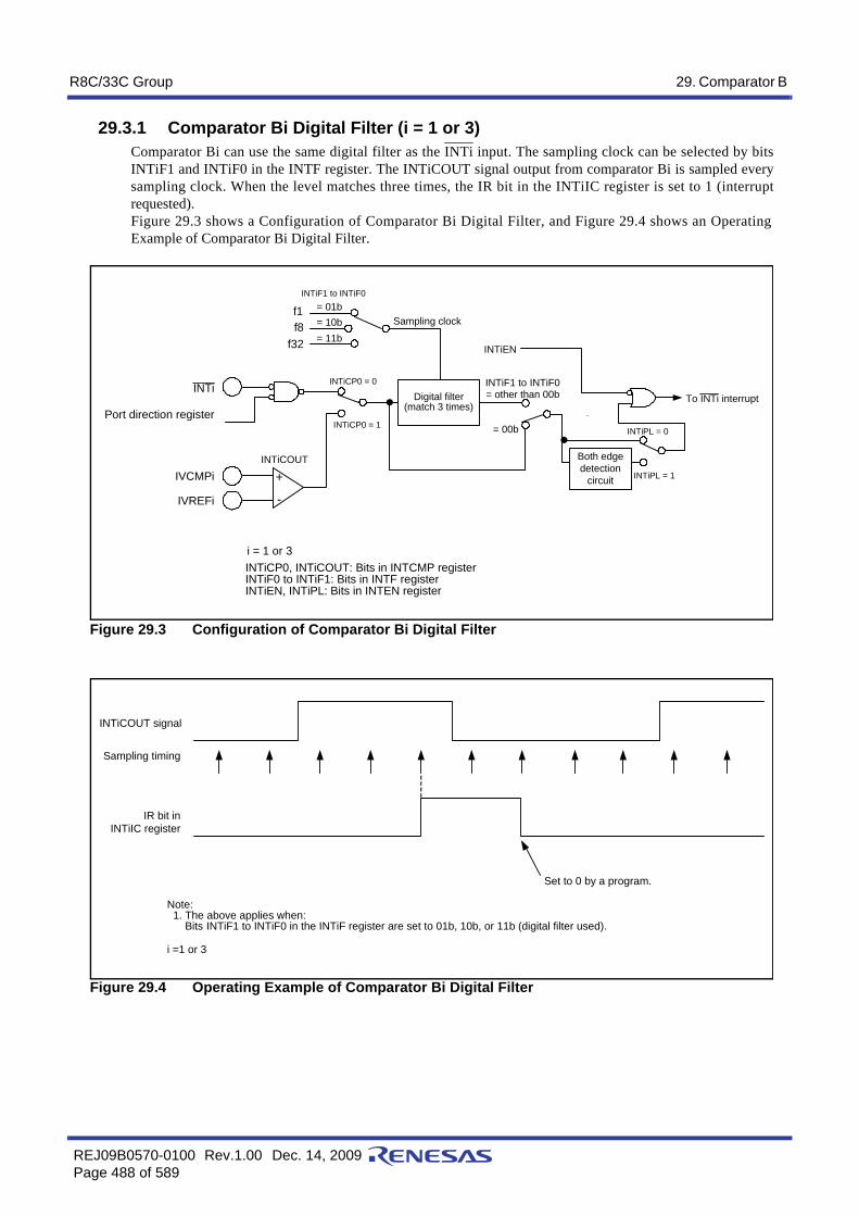
R8C/33C Group 29. Comparator B
REJ09B0570-0100 Rev.1.00 Dec. 14, 2009Page 488 of 589
29.3.1 Comparator Bi Digital Filter (i = 1 or 3)Comparator Bi can use the same digital filter as the INTi input. The sampling clock can be selected by bitsINTiF1 and INTiF0 in the INTF register. The INTiCOUT signal output from comparator Bi is sampled everysampling clock. When the level matches three times, the IR bit in the INTiIC register is set to 1 (interruptrequested). Figure 29.3 shows a Configuration of Comparator Bi Digital Filter, and Figure 29.4 shows an OperatingExample of Comparator Bi Digital Filter.
Figure 29.3 Configuration of Comparator Bi Digital Filter
Figure 29.4 Operating Example of Comparator Bi Digital Filter
= 01b
INTi
Port direction register
Sampling clock
To INTi interrupt
= 10b= 11bf32
f8f1
INTiF1 to INTiF0
INTiEN
INTiF1 to INTiF0= other than 00b
= 00b
INTiCP0, INTiCOUT: Bits in INTCMP registerINTiF0 to INTiF1: Bits in INTF registerINTiEN, INTiPL: Bits in INTEN register
INTiPL = 0
INTiPL = 1
i = 1 or 3
+
-
INTiCOUT
IVCMPi
IVREFi
INTiCP0 = 0
INTiCP0 = 1
Digital filter(match 3 times)
Both edgedetection
circuit
INTiCOUT signal
Sampling timing
IR bit inINTiIC register
Set to 0 by a program.
Note: 1. The above applies when: Bits INTiF1 to INTiF0 in the INTiF register are set to 01b, 10b, or 11b (digital filter used).
i =1 or 3

R8C/33C Group 29. Comparator B
REJ09B0570-0100 Rev.1.00 Dec. 14, 2009Page 489 of 589
29.4 Comparator B1 and Comparator B3 InterruptsComparator B generates an interrupt request from two sources, comparator B1 and comparator B3. Thecomparator Bi (i = 1 or 3) interrupt uses the same INTiIC register (bits IR and ILVL0 to ILVL2) as the INTi (i= 1 or 3) and a single vector. To use the comparator Bi interrupt, set the INTiEN bit in the INTEN register to 1 (interrupt enabled). Inaddition, the polarity can be selected by the INTiPL bit in the INTEN register and the POL bit in the INTiICregister. Inputs can also be passed through the digital filter with three different sampling clocks.

R8C/33C Group 30. Flash Memory
REJ09B0570-0100 Rev.1.00 Dec. 14, 2009Page 490 of 589
30. Flash MemoryThe flash memory can perform in the following three rewrite modes: CPU rewrite mode, standard serial I/O mode, andparallel I/O mode.
30.1 OverviewTable 30.1 lists the Flash Memory Version Performance. (Refer to Table 1.1 and Table 1.2 R8C/33C GroupSpecifications for items not listed in Table 30.1.)
Notes:1. To perform programming and erasure, use VCC = 2.7 V to 5.5 V as the supply voltage. Do not perform
programming and erasure at less than 2.7 V. 2. Definition of programming and erasure endurance
The programming and erasure endurance is defined on a per-block basis. If the programming and erasureendurance is n (n = 1,000 or 10,000), each block can be erased n times. For example, if 1,024 1-byte writes areperformed to different addresses in block A, a 1-Kbyte block, and then the block is erased, the programming/erasure endurance still stands at one. When performing 100 or more rewrites, the actual erase count can bereduced by executing program operations in such a way that all blank areas are used before performing anerase operation. Avoid rewriting only particular blocks and try to average out the programming and erasureendurance of the blocks. It is also advisable to retain data on the erasure endurance of each block and limit thenumber of erase operations to a certain number.
3. The number of blocks and block division vary with the MCU. Refer to Figure 30.1 R8C/33C Group FlashMemory Block Diagram for details.
Table 30.1 Flash Memory Version PerformanceItem Specification
Flash memory operating mode 3 modes (CPU rewrite, standard serial I/O, and parallel I/O)Division of erase blocks Refer to Figure 30.1.Programming method Byte unitsErasure method Block eraseProgramming and erasure control method (1) Program and erase control by software commandsRewrite control method
Blocks 0 to 3(Program ROM) (3)
Rewrite protect control in block units by the lock bit
Blocks A, B, C, and D(Data flash)
Individual rewrite protect control on blocks A, B, C, and D by bits FMR14, FMR15, FMR16, and FMR17 in the FMR1 register
Number of commands 7 commandsProgramming and erasure endurance (2)
Blocks 0 to 3(Program ROM) (3)
1,000 times
Blocks A, B, C, and D(Data flash)
10,000 times
ID code check function Standard serial I/O mode supportedROM code protection Parallel I/O mode supported
Table 30.2 Flash Memory Rewrite ModeFlash MemoryRewrite Mode CPU Rewrite Mode Standard Serial I/O Mode Parallel I/O Mode
Function User ROM area is rewritten by executing software commands from the CPU.
User ROM area is rewritten using a dedicated serial programmer.
User ROM area is rewritten using a dedicated parallel programmer.
Rewritable area User ROM User ROM User ROMRewrite programs User program Standard boot program –

R8C/33C Group 30. Flash Memory
REJ09B0570-0100 Rev.1.00 Dec. 14, 2009Page 491 of 589
30.2 Memory MapThe flash memory contains a user ROM area and a boot ROM area (reserved area). Figure 30.1 show the R8C/33C Group Flash Memory Block Diagrams.The user ROM area contains program ROM and data flash.Program ROM: Flash memory mainly used for storing programsData flash: Flash memory mainly used for storing data to be rewrittenThe user ROM area is divided into several blocks. The user ROM area can be rewritten in CPU rewrite mode,standard serial I/O mode, or parallel I/O mode.The rewrite control program (standard boot program) for standard serial I/O mode is stored in the boot ROM areabefore shipment. The boot ROM area is allocated separately from the user ROM area.
Figure 30.1 R8C/33C Group Flash Memory Block Diagram
Program ROM
Data flash
User ROM area
0F7FFh
03000h
03FFFh
ROM 8 KB product
Block B: 1 Kbyte
Block A: 1 Kbyte
Block C: 1 Kbyte
Block D: 1 Kbyte
Block 2: 4 Kbytes
Block 0: 2 KbytesUser ROM area
03000h
03FFFh
ROM 4 KB product
Block B: 1 Kbyte
Block A: 1 Kbyte
Block C: 1 Kbyte
Block D: 1 Kbyte
0E000h0EFFFh0F000h Block 1: 2 Kbytes0F800h0FFFFh
0F7FFhBlock 0: 2 Kbytes
0F000h Block 1: 2 Kbytes0F800h0FFFFh
Program ROM
Data flash
03FFFh
User ROM area
0C000h
0FFFFh
03000hROM 16 KB product
Block B: 1 Kbyte
Block A: 1 Kbyte
Block C: 1 Kbyte
Block D: 1 Kbyte
Block 2: 8 Kbytes
Block 1: 4 KbytesBlock 0: 4 Kbytes
0E000h0F000h
08000h
User ROM area
0BFFFh0C000h
0FFFFh
03000h
03FFFh
ROM 32 KB product
Block B: 1 Kbyte
Block A: 1 Kbyte
Block C: 1 Kbyte
Block D: 1 Kbyte
Block 2: 8 Kbytes
Block 3: 16 Kbytes
Block 1: 4 KbytesBlock 0: 4 Kbytes
0F000h0E000h
User ROM area
0C000h
03000hROM 24 KB product
0FFFFh
0A000h
03FFFh
Block B: 1 Kbyte
Block A: 1 Kbyte
Block C: 1 Kbyte
Block D: 1 Kbyte
Block 2: 8 Kbytes
Block 1: 4 KbytesBlock 0: 4 Kbytes
Block 3: 8 Kbytes
0F000h0E000h
0BFFFh

R8C/33C Group 30. Flash Memory
REJ09B0570-0100 Rev.1.00 Dec. 14, 2009Page 492 of 589
30.3 Functions to Prevent Flash Memory from being RewrittenStandard serial I/O mode has an ID code check function, and parallel I/O mode has a ROM code protect function toprevent the flash memory from being read or rewritten easily.
30.3.1 ID Code Check FunctionThe ID code check function is used in standard serial I/O mode. Unless 3 bytes (addresses 0FFFCh to 0FFFEh)of the reset vector are set to FFFFFFh, the ID codes sent from the serial programmer or the on-chip debuggingemulator and the 7-byte ID codes written in the flash memory are checked to see if they match. If the ID codesdo not match, the commands sent from the serial programmer or the on-chip debugging emulator are notaccepted. For details of the ID code check function, refer to 12. ID Code Areas.

R8C/33C Group 30. Flash Memory
REJ09B0570-0100 Rev.1.00 Dec. 14, 2009Page 493 of 589
30.3.2 ROM Code Protect FunctionThe ROM protect function prevents the contents of the flash memory from being read, rewritten, or erasedusing the OFS register in parallel I/O mode.Refer to 13. Option Function Select Area for details of the option function select area.
The ROM code protect function is enabled by writing 1 to the ROMCR bit and writing 0 to the ROMCP1 bit.This prevents the contents of the on-chip flash memory from being read or rewritten. Once ROM code protection is enabled, the content of the internal flash memory cannot be rewritten in parallelI/O mode. To disable ROM code protection, erase the block including the OFS register using CPU rewrite modeor standard serial I/O mode.
30.3.3 Option Function Select Register (OFS)
Notes:1. The OFS register is allocated in the flash memory, not in the SFRs. Set appropriate values as ROM data by a
program.Do not write additions to the OFS register. If the block including the OFS register is erased, the OFS register isset to FFh.When blank products are shipped, the OFS register is set to FFh. It is set to the written value after written by theuser.When factory-programming products are shipped, the value of the OFS register is the value programmed by theuser.
2. The same level of the voltage detection 0 level selected by bits VDSEL0 and VDESL1 is set in both functions ofvoltage monitor 0 reset and power-on reset.
3. To use power-on reset and voltage monitor 0 reset, set the LVDAS bit to 0 (voltage monitor 0 reset enabled afterreset).
For a setting example of the OFS register, refer to 13.3.1 Setting Example of Option Function Select Area.
LVDAS Bit (Voltage Detection 0 Circuit Start Bit)The Vdet0 voltage to be monitored by the voltage detection 0 circuit is selected by bits VDSEL0 and VDSEL1.
Address 0FFFFhBit b7 b6 b5 b4 b3 b2 b1 b0
Symbol CSPROINI LVDAS VDSEL1 VDSEL0 ROMCP1 ROMCR — WDTONAfter Reset User Setting Value (1)
Bit Symbol Bit Name Function R/Wb0 WDTON Watchdog timer start select bit 0: Watchdog timer automatically starts after reset
1: Watchdog timer is stopped after resetR/W
b1 — Reserved bit Set to 1. R/Wb2 ROMCR ROM code protect disable bit 0: ROM code protect disabled
1: ROMCP1 bit enabledR/W
b3 ROMCP1 ROM code protect bit 0: ROM code protect enabled1: ROM code protect disabled
R/W
b4 VDSEL0 Voltage detection 0 level select bit (2) b5 b4 0 0: 3.80 V selected (Vdet0_3) 0 1: 2.85 V selected (Vdet0_2) 1 0: 2.35 V selected (Vdet0_1) 1 1: 1.90 V selected (Vdet0_0)
R/Wb5 VDSEL1 R/W
b6 LVDAS Voltage detection 0 circuit start bit (3) 0: Voltage monitor 0 reset enabled after reset1: Voltage monitor 0 reset disabled after reset
R/W
b7 CSPROINI Count source protection mode after reset select bit
0: Count source protect mode enabled after reset1: Count source protect mode disabled after reset
R/W

R8C/33C Group 30. Flash Memory
REJ09B0570-0100 Rev.1.00 Dec. 14, 2009Page 494 of 589
30.4 CPU Rewrite ModeIn CPU rewrite mode, the user ROM area can be rewritten by executing software commands from the CPU.Therefore, the user ROM area can be rewritten directly while the MCU is mounted on a board without using aROM programmer. Execute the software command only to blocks in the user ROM area.The flash module has an erase-suspend function which halts the erase operation temporarily during an eraseoperation in CPU rewrite mode. During erase-suspend, the flash memory can be read or programmed.Erase-write 0 mode (EW0 mode) and erase-write 1 mode (EW1 mode) are available in CPU rewrite mode. Table 30.3 lists the Differences between EW0 Mode and EW1 Mode.
Table 30.3 Differences between EW0 Mode and EW1 ModeItem EW0 Mode EW1 Mode
Operating mode Single-chip mode Single-chip modeRewrite control program allocatable area
User ROM User ROM
Rewrite control program executable areas
RAM (The rewrite control program must be transferred before being executed.)However, the program can be executed in the program ROM area when rewriting the data flash area.
User ROM or RAM
Rewritable area User ROM User ROMHowever, blocks which contain the rewrite control program are excluded.
Software command restrictions
— Program and block erase commandsCannot be executed to any block which contains the rewrite control program.
Mode after programming or block erasure or after entering erase-suspend
Read array mode Read array mode
CPU state during programming and block erasure
The CPU operates. • The CPU operates while the data flash area is being programmed or block erased.
• The CPU is put in a hold state while the program ROM area is being programmed or block erased. (I/O ports retain the state before the command execution).
Flash memory status detection
Read bits FST7, FMT5, and FMT4 in the FST register by a program.
Read bits FST7, FMT5, and FMT4 in the FST register by a program.
Conditions for entering erase-suspend
• Set bits FMR20 and FMR21 in the FMR2 register to 1 by a program.
• Set bits FMR20 and FMR22 in the FMR2 register to 1 and the enabled maskable interrupt is generated.
• Set bits FMR20 and FMR21 in the FMR2 register to 1 by a program (while rewriting the data flash area).
• Set bits FMR20 and FMR22 in the FMR2 register to 1 and the enabled maskable interrupt is generated.
CPU clock Max. 20 MHz Max. 20 MHz

R8C/33C Group 30. Flash Memory
REJ09B0570-0100 Rev.1.00 Dec. 14, 2009Page 495 of 589
30.4.1 Flash Memory Status Register (FST)
Notes:1. The RDYSTI bit cannot be set to 1 (flash ready status interrupt request) by a program.2. The BSYAEI bit cannot be set to 1 (flash access error interrupt request) by a program.3. This bit is also set to 1 (error) when a command error occurs.4. When this bit is set to 1, dot not set the FMR01 bit in the FMR0 register to 0 (CPU rewrite mode disabled).
RDYSTI Bit (Flash Ready Status Flag Interrupt Request Flag)When the RDYSTIE bit in the FMR0 register is set to 1 (flash ready status interrupt enabled) and auto-programming or auto-erasure completes, or erase-suspend mode is entered, the RDYSTI bit is set to 1 (flashready status interrupt request).During interrupt handling, set the RDYSTI bit to 0 (no flash ready status interrupt request).
[Condition for setting to 0]Set to 0 by an interrupt handling program.[Condition for setting to 1]When the flash memory status changes from busy to ready while the RDYSTIE bit in the FRMR0 register is setto 1, the RDYSTI bit is set to 1. The status is changed from busy to ready in the following states:• Completion of erasing/programming the flash memory• Suspend acknowledgement• Completion of forcible termination• Completion of the lock bit program• Completion of the read lock bit status• Completion of the block blank check• When the flash memory can be read after it has been stopped.
Address 01B2hBit b7 b6 b5 b4 b3 b2 b1 b0
Symbol FST7 FST6 FST5 FST4 — LBDATA BSYAEI RDYSTIAfter Reset 1 0 0 0 0 X 0 0
Bit Symbol Bit Name Function R/Wb0 RDYSTI Flash ready status interrupt request
flag (1, 4)0: No flash ready status interrupt request 1: Flash ready status interrupt request
R/W
b1 BSYAEI Flash access error interrupt request flag (2, 4)
0: No flash access error interrupt request1: Flash access error interrupt request
R/W
b2 LBDATA LBDATA monitor flag 0: Locked1: Not locked
R
b3 — Nothing is assigned. If necessary, set to 0. When read, the content is 0. —b4 FST4 Program error flag (3) 0: No program error
1: Program errorR
b5 FST5 Erase error/blank check error flag (3) 0: No erase error/blank check error1: Erase error/blank check error
R
b6 FST6 Erase-suspend status flag 0: Other than erase-suspend1: During erase-suspend
R
b7 FST7 Ready/busy status flag 0: Busy1: Ready
R

R8C/33C Group 30. Flash Memory
REJ09B0570-0100 Rev.1.00 Dec. 14, 2009Page 496 of 589
BSYAEI Bit (Flash Access Error Interrupt Request Flag)The BYSAEI bit is set to 1 (flash access error interrupt request) when the BSYAEIE bit in the FMR0 register isset to 1 (flash access error interrupt enabled) and the block during auto-programming/auto-erasure is accessed.This bit is also set to 1 if an erase or program error occurs when the CMDERIE bit in the FMR0 register is set to1 (erase/write error interrupt enabled).During interrupt handling, set the BSYAEI bit to 0 (no flash access error interrupt request).
[Conditions for setting to 0](1) Set to 0 by an interrupt handling program.(2) Execute the clear status register command.[Conditions for setting to 1](1) Read or write the area that is being erased/written when the BSYAEIE bit in the FRMR0 register is set to 1
and while the flash memory is busy.Or, read the data flash area while erasing/writing to the program ROM area. (Note that the read value isundefined in both cases. Writing has no effect.)
(2) If a command sequence error, erase error, blank check error, or program error occurs when the CMDERIEbit in the FMR0 register is set to 1 (erase/write error interrupt enabled).
LBDATA Bit (LBDATA Monitor Flag)This is a read-only bit indicating the lock bit status. To confirm the lock bit status, execute the read lock bitstatus command and read the LBDATA bit after the FST7 bit is set to 1 (ready). The condition for updating this bit is when the program, erase, read lock bit status commands are generated. When the read lock bit status command is input, the FST7 bit is set to 0 (busy). At the time when the FST7 bitis set to 1 (ready), the lock bit status is stored in the LBDATA bit. The data in the LBDATA bit is retained untilthe next command is input.
FST4 Bit (Program Error Flag)This is a read-only bit indicating the auto-programming status. The bit is set to 1 if a program error occurs;otherwise, it is set to 0. For details, refer to the description in 30.4.12 Full Status Check.
FST5 Bit (Erase Error/Blank Check Error Flag)This is a read-only bit indicating the status of auto-programming or the block blank check command. The bit isset to 1 if an erase error or blank check error occurs; otherwise, it is set to 0. Refer to 30.4.12 Full Status Checkfor details.
FST6 Bit (Erase Suspend Status Flag)This is a read-only bit indicating the suspend status. The bit is set to 1 when an erase-suspend request isacknowledged and a suspend status is entered; otherwise, it is set to 0.
FST7 Bit (Ready/Busy Status Flag)When the FST7 bit is set to 0 (busy), the flash memory is in one of the following states:• During programming• During erasure• During the lock bit program• During the read lock bit status• During the block blank check• During forced stop operation• The flash memory is being stopped• The flash memory is being activatedOtherwise, the FST7 bit is set to 1 (ready).

R8C/33C Group 30. Flash Memory
REJ09B0570-0100 Rev.1.00 Dec. 14, 2009Page 497 of 589
30.4.2 Flash Memory Control Register 0 (FMR0)
Notes:1. To set this bit to 1, first write 0 and then 1 immediately. Disable interrupts and DTC activation between writing 0
and writing 1.2. Write to the FMSTP bit by a program transferred to the RAM. The FMSTP bit is enabled when the FMR01 bit is
set to 1 (CPU rewrite mode enabled). To set the FMSTP bit to 1 (flash memory stops), set it when the FST7 bit inthe FST register is set to 1 (ready).
3. The CMDRST bit is enabled when the FMR01 bit is set to 1 (CPU rewrite mode enabled) and the FST7 bit in theFST register is set to 0 (busy).
4. To set the FMR01 bit to 0 (CPU rewrite mode disabled), set it when the RDYSTI bit in the FST register is set to 0(no flash ready status interrupt request) and the BSYAEI bit is set to 0 (no flash access error interrupt request).
FMR01 Bit (CPU Rewrite Mode Select Bit)When the FMR01 bit is set to 1 (CPU rewrite mode enabled), the MCU is made ready to accept softwarecommands.
FMR02 Bit (EW1 Mode Select Bit)When the FMR02 bit is set to 1 (EW1 mode), EW1 mode is selected.
Address 01B4hBit b7 b6 b5 b4 b3 b2 b1 b0
Symbol RDYSTIE BSYAEIE CMDERIE CMDRST FMSTP FMR02 FMR01 —After Reset 0 0 0 0 0 0 0 0
Bit Symbol Bit Name Function R/Wb0 — Reserved bit Set to 0. R/Wb1 FMR01 CPU rewrite mode select bit (1, 4) 0: CPU rewrite mode disabled
1: CPU rewrite mode enabledR/W
b2 FMR02 EW1 mode select bit (1) 0: EW0 mode1: EW1 mode
R/W
b3 FMSTP Flash memory stop bit (2) 0: Flash memory operates1: Flash memory stops
(Low-power consumption state, flash memory initialization)
R/W
b4 CMDRST Erase/write sequence reset bit (3) When the CMDRST bit is set to 1, the erase/write sequence is reset and erasure/writing can be forcibly stopped.When read, the content is 0.
R/W
b5 CMDERIE Erase/write error interrupt enable bit 0: Erase/write error interrupt disabled1: Erase/write error interrupt enabled
R/W
b6 BSYAEIE Flash access error interrupt enable bit 0: Flash access error interrupt disabled1: Flash access error interrupt enabled
R/W
b7 RDYSTIE Flash ready status interrupt enable bit 0: Flash ready status interrupt disabled1: Flash ready status interrupt enabled
R/W

R8C/33C Group 30. Flash Memory
REJ09B0570-0100 Rev.1.00 Dec. 14, 2009Page 498 of 589
FMSTP Bit (Flash Memory Stop Bit)This bit is used to initialize the flash memory control circuits, and also to reduce the amount of currentconsumed by the flash memory. Access to the flash memory is disabled by setting the FMSTP bit to 1.Write to the FMSTP bit by a program transferred to the RAM.To reduce the power consumption further in high-speed on-chip oscillator mode, low-speed on-chip oscillatormode (XIN clock stopped), and low-speed clock mode (XIN clock stopped), set the FMSTP bit to 1. Refer to31.2.10 Stopping Flash Memory for details.When entering stop mode or wait mode while CPU rewrite mode is disabled, the FMR0 register does not needto be set because the power for the flash memory is automatically turned off and is turned back on when exitingstop or wait mode. When the FMSTP bit is set to 1 (including during the busy status (the period while the FST7 bit is 0)immediately after the FMSTP bit is changed from 1 to 0), do not set to low-current-consumption read mode atthe same time.
Figure 30.2 Transition to Low-Current-Consumption Read Mode
CMDRST Bit (Erase/Write Sequence Reset Bit)This bit is used to initialize the flash memory sequence and forcibly stop a program or erase command. Theprogram ROM area can be read when resetting the sequence of programming/erasing the data flash area.If the program or erase command is forcibly stopped using the CMDRST bit in the FMR0 register, execute theclear status command after the FST7 bit in the FST register is changed to 1 (ready). To program to the sameaddress again, execute the block erase command again and ensure it has been completed normally beforeprogramming. If the addresses and blocks which the program or block erase command is forcibly stopped areallocated in the program area, set the FMR13 bit in the FMR1 register to 1 (lock bit disabled) before executingthe block erasure command again.When the CMDRST bit is set to 1 (erasure/writing stopped) during erase-suspend, the suspend status is alsoinitialized. Thus execute block erasure again to the block which the block erasure is being suspended.When td(CMDRST-READY) has elapsed after the CMDRST bit is set to 1 (erasure/writing stopped), theexecuting command is forcibly terminated and reading from the flash memory is enabled.
CMDERIE Bit (Erase/Write Error Interrupt Enable Bit)This bit enables an flash command error interrupt to be generated if the following errors occur:• Program error• Block erase error• Command sequence error• Block blank check errorIf the CMDERIE bit is set to 1 (erase/write error interrupt enabled), an interrupt is generated if the above errorsoccur.If a flash command error interrupt is generated, execute the clear status register command during interrupthandling.
BSYAEIE Bit (Flash Access Error Interrupt Enable Bit)This bit enables a flash access error interrupt to be generated if the flash memory during rewriting is accessed.
RDYSTIE Bit (Flash Ready Status Interrupt Enable Bit)This bit enables a flash ready status error interrupt to be generated when the status of the flash memorysequence changes from the busy to ready status.
FMSTP bit
FST7 bit 0 (busy) 1 (ready)
Do not set to low-current-consumption read mode.Low-current-consumption
read mode enabled

R8C/33C Group 30. Flash Memory
REJ09B0570-0100 Rev.1.00 Dec. 14, 2009Page 499 of 589
30.4.3 Flash Memory Control Register 1 (FMR1)
Notes:1. To set the FMR13 bit to 1, first write 0 and then 1 immediately. Disable interrupts and DTC activation between
writing 0 and writing 1.2. To set this bit to 0, first write 1 and then 0 immediately. Disable interrupts and DTC activation between writing 1
and writing 0.3. This bit is set to 0 when the FMR01 bit in the FMR0 register is set to 0 (CPU rewrite mode disabled).
FMR13 Bit (Lock Bit Disable Select Bit)When the FMR13 bit is set to 1 (lock bit disabled), the lock bit is disabled. When the FMR13 bit is set to 0, thelock bit is enabled. Refer to 30.4.10 Data Protect Function for the details of the lock bit. The FMR13 bit enables the lock bit function only and the lock bit data does not change. However, when a blockerase command is executed while the FMR13 bit is set to 1, the lock bit data set to 0 (locked) changes to 1 (notlocked) after erasure completes.
[Conditions for setting to 0]The FMR13 bit is set to 0 when one of the following conditions is met. • Completion of the program command• Completion of the erase command• Generation of a command sequence error• Transition to erase-suspend• If the FMR01 bit in the FMR0 register is set to 0 (CPU rewrite mode disabled).• If the FMSTP bit in the FMR0 register is set to 1 (flash memory stops).• If the CMDRST bit in the FMR0 register is set to 1 (erasure/writing stopped).[Condition for setting to 1]Set to 1 by a program.
Address 01B5hBit b7 b6 b5 b4 b3 b2 b1 b0
Symbol FMR17 FMR16 FMR15 FMR14 FMR13 FMR12 FMR11 FMR10After Reset 0 0 0 0 0 0 0 0
Bit Symbol Bit Name Function R/Wb0 FMR10 Nothing is assigned. If necessary, set to 0. When read, the content is 0. —b1 FMR11b2 FMR12b3 FMR13 Lock bit disable select bit (1) 0: Lock bit enabled
1: Lock bit disabledR/W
b4 FMR14 Data flash block A rewrite disable bit (2, 3)
0: Rewrite enabled (software command acceptable)1: Rewrite disabled (software command not acceptable,
no error occurred)
R/W
b5 FMR15 Data flash block B rewrite disable bit (2, 3)
0: Rewrite enabled (software command acceptable)1: Rewrite disabled (software command not acceptable,
no error occurred)
R/W
b6 FMR16 Data flash block C rewrite disable bit (2, 3)
0: Rewrite enabled (software command acceptable)1: Rewrite disabled (software command not acceptable,
no error occurred)
R/W
b7 FMR17 Data flash block D rewrite disable bit (2, 3)
0: Rewrite enabled (software command acceptable)1: Rewrite disabled (software command not acceptable,
no error occurred)
R/W

R8C/33C Group 30. Flash Memory
REJ09B0570-0100 Rev.1.00 Dec. 14, 2009Page 500 of 589
FMR14 Bit (Data Flash Block A Rewrite Disable Bit)When the FMR 14 bit is set to 0, data flash block A accepts program and block erase commands.
FMR15 Bit (Data Flash Block B Rewrite Disable Bit)When the FMR 15 bit is set to 0, data flash block B accepts program and block erase commands.
FMR16 Bit (Data Flash Block C Rewrite Disable Bit)When the FMR 16 bit is set to 0, data flash block C accepts program and block erase commands.
FMR17 Bit (Data Flash Block D Rewrite Disable Bit)When the FMR 17 bit is set to 0, data flash block D accepts program and block erase commands.
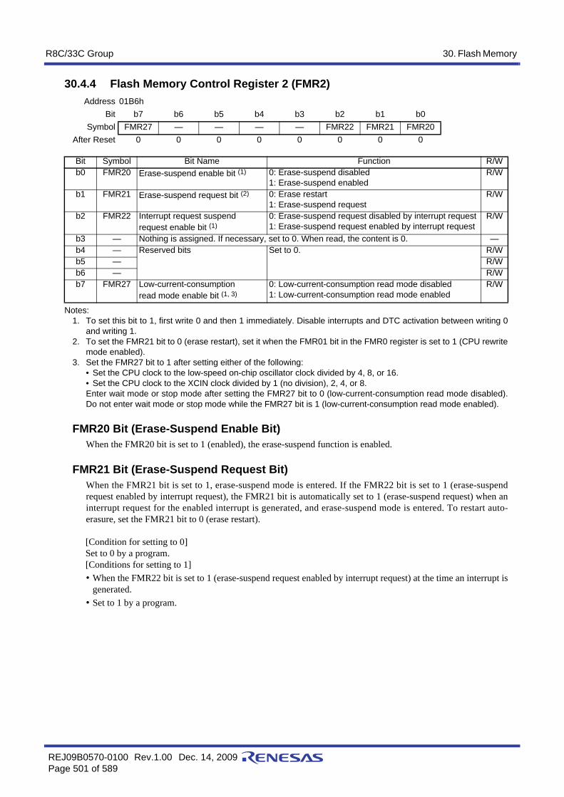
R8C/33C Group 30. Flash Memory
REJ09B0570-0100 Rev.1.00 Dec. 14, 2009Page 501 of 589
30.4.4 Flash Memory Control Register 2 (FMR2)
Notes:1. To set this bit to 1, first write 0 and then 1 immediately. Disable interrupts and DTC activation between writing 0
and writing 1.2. To set the FMR21 bit to 0 (erase restart), set it when the FMR01 bit in the FMR0 register is set to 1 (CPU rewrite
mode enabled).3. Set the FMR27 bit to 1 after setting either of the following:
• Set the CPU clock to the low-speed on-chip oscillator clock divided by 4, 8, or 16.• Set the CPU clock to the XCIN clock divided by 1 (no division), 2, 4, or 8.Enter wait mode or stop mode after setting the FMR27 bit to 0 (low-current-consumption read mode disabled).Do not enter wait mode or stop mode while the FMR27 bit is 1 (low-current-consumption read mode enabled).
FMR20 Bit (Erase-Suspend Enable Bit)When the FMR20 bit is set to 1 (enabled), the erase-suspend function is enabled.
FMR21 Bit (Erase-Suspend Request Bit)When the FMR21 bit is set to 1, erase-suspend mode is entered. If the FMR22 bit is set to 1 (erase-suspendrequest enabled by interrupt request), the FMR21 bit is automatically set to 1 (erase-suspend request) when aninterrupt request for the enabled interrupt is generated, and erase-suspend mode is entered. To restart auto-erasure, set the FMR21 bit to 0 (erase restart).
[Condition for setting to 0]Set to 0 by a program. [Conditions for setting to 1]• When the FMR22 bit is set to 1 (erase-suspend request enabled by interrupt request) at the time an interrupt is
generated.• Set to 1 by a program.
Address 01B6hBit b7 b6 b5 b4 b3 b2 b1 b0
Symbol FMR27 — — — — FMR22 FMR21 FMR20After Reset 0 0 0 0 0 0 0 0
Bit Symbol Bit Name Function R/Wb0 FMR20 Erase-suspend enable bit (1) 0: Erase-suspend disabled
1: Erase-suspend enabledR/W
b1 FMR21 Erase-suspend request bit (2) 0: Erase restart1: Erase-suspend request
R/W
b2 FMR22 Interrupt request suspend request enable bit (1)
0: Erase-suspend request disabled by interrupt request1: Erase-suspend request enabled by interrupt request
R/W
b3 — Nothing is assigned. If necessary, set to 0. When read, the content is 0. —b4 — Reserved bits Set to 0. R/Wb5 — R/Wb6 — R/Wb7 FMR27 Low-current-consumption
read mode enable bit (1, 3)0: Low-current-consumption read mode disabled1: Low-current-consumption read mode enabled
R/W

R8C/33C Group 30. Flash Memory
REJ09B0570-0100 Rev.1.00 Dec. 14, 2009Page 502 of 589
FMR22 Bit (Interrupt Request Suspend-Request Enable Bit)When the FMR 22 bit is set to 1 (erase-suspend request enabled by interrupt request), the FMR21 bit isautomatically set to 1 (erase-suspend request) at the time an interrupt request is generated during auto-erasure.Set the FMR22 bit to 1 when using erase-suspend while rewriting the user ROM area in EW1 mode.
FMR27 Bit (Low-Current-Consumption Read Mode Enable Bit)When the FMR 27 bit is set to 1 (low-current-consumption read mode enabled) in low-speed clock mode (XINclock stopped) or low-speed on-chip oscillator mode (XIN clock stopped), power consumption when readingthe flash memory can be reduced. Refer to 31.2.11 Low-Current-Consumption Read Mode for details.Low-current-consumption read mode can be used when the CPU clock is set to either of the following:• The CPU clock is set to the low-speed on-chip oscillator clock divided by 4, 8, or 16.• The CPU clock is set to the XCIN clock divided by 1 (no division), 2, 4, or 8.However, do not use low-current-consumption read mode when the frequency of the selected CPU clock is3 kHz or below. After setting the divide ratio of the CPU clock, set the FMR27 bit to 1.Enter wait mode or stop mode after setting the FMR27 bit to 0 (low-current-consumption read mode disabled).Do not enter wait mode or stop mode while the FMR27 bit is 1 (low-current-consumption read mode enabled).When the FMR27 bit is set to 1 (low-current-consumption read mode enabled), do not execute the program,block erase, or lock bit program command. To change the FMSTP bit from 1 (flash memory stops) to 0 (flashmemory operates), make the setting when the FMR27 bit is set to 0 (low-current-consumption read modedisabled).
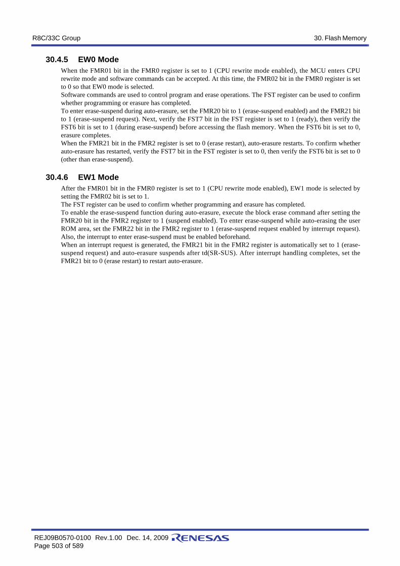
R8C/33C Group 30. Flash Memory
REJ09B0570-0100 Rev.1.00 Dec. 14, 2009Page 503 of 589
30.4.5 EW0 ModeWhen the FMR01 bit in the FMR0 register is set to 1 (CPU rewrite mode enabled), the MCU enters CPUrewrite mode and software commands can be accepted. At this time, the FMR02 bit in the FMR0 register is setto 0 so that EW0 mode is selected.Software commands are used to control program and erase operations. The FST register can be used to confirmwhether programming or erasure has completed.To enter erase-suspend during auto-erasure, set the FMR20 bit to 1 (erase-suspend enabled) and the FMR21 bitto 1 (erase-suspend request). Next, verify the FST7 bit in the FST register is set to 1 (ready), then verify theFST6 bit is set to 1 (during erase-suspend) before accessing the flash memory. When the FST6 bit is set to 0,erasure completes.When the FMR21 bit in the FMR2 register is set to 0 (erase restart), auto-erasure restarts. To confirm whetherauto-erasure has restarted, verify the FST7 bit in the FST register is set to 0, then verify the FST6 bit is set to 0(other than erase-suspend).
30.4.6 EW1 ModeAfter the FMR01 bit in the FMR0 register is set to 1 (CPU rewrite mode enabled), EW1 mode is selected bysetting the FMR02 bit is set to 1. The FST register can be used to confirm whether programming and erasure has completed.To enable the erase-suspend function during auto-erasure, execute the block erase command after setting theFMR20 bit in the FMR2 register to 1 (suspend enabled). To enter erase-suspend while auto-erasing the userROM area, set the FMR22 bit in the FMR2 register to 1 (erase-suspend request enabled by interrupt request).Also, the interrupt to enter erase-suspend must be enabled beforehand.When an interrupt request is generated, the FMR21 bit in the FMR2 register is automatically set to 1 (erase-suspend request) and auto-erasure suspends after td(SR-SUS). After interrupt handling completes, set theFMR21 bit to 0 (erase restart) to restart auto-erasure.

R8C/33C Group 30. Flash Memory
REJ09B0570-0100 Rev.1.00 Dec. 14, 2009Page 504 of 589
30.4.7 Suspend OperationThe suspend function halts the auto-erase operation temporarily during auto-erasure.When auto-erasure is suspended, the next operation can be executed. (Refer to Table 30.4 ExecutableOperation during Suspend.)• When suspending the auto-erasure of any block in data flash, auto-programming and reading another block
can be executed.• When suspending the auto-erasure of data flash, auto-programming and reading program ROM can be
executed. • When suspending the auto-erasure of any block in program ROM, auto-programming and reading another
block can be executed. • When suspending the auto-erasure of program ROM, auto-programming and reading data flash can be
executed.• To check the suspend, verify the FST7 bit is set to 1 (ready), then verify the FST6 bit is set to 1 (during erase-
suspend) to confirm whether erasure has been suspended. When the FST6 bit is set to 0 (other than erasesuspend), erasure completes.
Figure 30.3 shows the Suspend Operation Timing.
Notes:1. E indicates operation is enabled by using the suspend function, D indicates operation is disabled, and N/A
indicates no combination is available.2. Operation cannot be suspended during programming.3. The block erase command can be executed for erasure. The program, lock bit program, and read lock bit status
commands can be executed for programming.The clear status register command can be executed when the FST7 bit in the FST register is set to 1 (ready).The operation of block blank check is disabled during suspend.
4. The MCU enters read array mode immediately after entering erase-suspend.5. The program ROM area can be read with the BGO function while programming or block erasing data flash.
Figure 30.3 Suspend Operation Timing
Table 30.4 Executable Operation during SuspendOperation during Suspend
Data flash(Block during erasure
execution before entering suspend)
Data flash(Block during no erasure
execution before entering suspend)
Program ROM(Block during erasure
execution before entering suspend)
Program ROM(Block during no erasure
execution before entering suspend)
Erase Program Read Erase Program Read Erase Program Read Erase Program ReadAreas during erasure execution before entering suspend
Data flash D D D D E E N/A N/A N/A D E E (5)
Program ROM N/A N/A N/A D E E D D D D E E
Data flashDataread
Suspend(readable) Program Erase
ProgramROM
Userprogram
Commandissue
Userprogram
SetFMR21bit to 1
Commandissue
Userprogram
SetFMR21bit to 0
Userprogram
Userprogram
FMR21 bit inFMR2 register
FST7 bit inFST register
FST6 bit inFST register
RDYSTI bit inFST register
Flash readyinterrupthandling
Suspend(readable)
Flash readyinterrupthandling
Userprogram
Flash readyinterrupthandling
Suspend(readable)
Set to 0 by a program. Set to 0 by a program. Set to 0 by a program.
td(SR-SUS)
1 is set automatically.
Erase
1 is set automatically. 1 is set automatically.

R8C/33C Group 30. Flash Memory
REJ09B0570-0100 Rev.1.00 Dec. 14, 2009Page 505 of 589
30.4.8 How to Set and Exit Each ModeFigure 30.4 shows How to Set and Exit EW0 Mode and Figure 30.5 shows How to Set and Exit EW0 Mode(When Rewriting Data Flash) and EW1 Mode.
Figure 30.4 How to Set and Exit EW0 Mode
Figure 30.5 How to Set and Exit EW0 Mode (When Rewriting Data Flash) and EW1 Mode
Transfer the rewrite mode program that usesCPU rewrite mode to the RAM
Jump to the rewrite control program transferredto the RAM(The subsequent process is executed by therewrite control program in the RAM)
After writing 0 to the FMR01 bit,write 1 (CPU rewrite mode enabled) (1)
Execute software commands
Write 0 (CPU rewrite mode disabled) tothe FMR01 bit
Jump to the specified address in the flash memory
Rewrite control program
Note: To set the FMR01 bit to 1, first write 0 and then 1 immediately. Disable interrupts and DTC activation between writing 0 and writing 1. Writing to the FMR01 bit must be performed in the RAM.
EW0 Mode Execution Procedure(When Rewriting User ROM)
FMR01: Bit in FMR0 register
After writing 0 to the FMR01 bit,write 1 (CPU rewrite mode enabled) (1)
Execute software commands
Write 0 (CPU rewrite mode disabled) tothe FMR01 bit
Notes: 1. To set the FMR01 bit to 1, first write 0 and then 1 immediately.
Disable interrupts and DTC activation between writing 0 and writing 1. 2. Not required when rewriting the data flash in EW0 mode.
EW0 Mode Execution Procedure (When Rewriting Data Flash)EW1 Mode Execution Procedure
Program in ROM
After writing 0 to the FMR02 bit,write 1 (EW1 mode) (2)
FMR01, FMR02: Bits in FMR0 register

R8C/33C Group 30. Flash Memory
REJ09B0570-0100 Rev.1.00 Dec. 14, 2009Page 506 of 589
30.4.9 BGO (BackGround Operation) FunctionWhen the program ROM area is specified while a program or block erase operation to the data flash, array datacan be read. This eliminates the need for writing software commands. Access time is the same as for normalread operations.Any other block of the data flash cannot read during a program or block erase operation to the data flash.Figure 30.6 shows the BGO Function.
Figure 30.6 BGO Function
Time
Data flash
Program ROM
Erase/program
Read Read Read Read

R8C/33C Group 30. Flash Memory
REJ09B0570-0100 Rev.1.00 Dec. 14, 2009Page 507 of 589
30.4.10 Data Protect FunctionEach block in the flash memory has a nonvolatile lock bit. The lock bit is enabled by setting the FMR13 bit inthe FMR1 register is set to 0 (lock bit enabled). The lock bit can be used to disable (lock) programming orerasing each block. This prevents data from being written or erased inadvertently. A block status changesaccording to the lock bit as follows:
• When the lock bit data is set to 0: locked (the block cannot be programmed or erased)• When the lock bit data is set to 1: not locked (the block can be programmed and erased)
The lock bit data is set to 0 (locked) by executing the lock bit program command and to 1 (not locked) byerasing the block. No commands can be used to set only the lock bit data to 1.The lock bit data can be read using the read lock bit status command.
When the FMR13 bit is set to 1 (lock bit disabled), the lock bit function is disabled and all blocks are not locked(each lock bit data remains unchanged). The lock bit function is enabled by setting the FMR13 bit to 0 (the lockbit data is retained).When the block erase command is executed while the FMR13 bit is set to 1, the target block is erased regardlessof the lock bit status. The lock bit of the erase target block is set to 1 after auto-erasure completes. Refer to 30.4.11 Software Commands for the details of individual commands.The FMR13 bit is set to 0 after auto-erasure completes. This bit is also set to 0 if one of the following conditionsis met. To erase or program a different locked block, set the FMR 13 bit to 1 again and execute the block eraseor program command.
• If the FST7 bit in the FST register is changed from 0 (busy) to 1 (ready).• If a command sequence error occurs.• If the FMR01 bit in the FMR0 register is set to 0 (CPU mode disabled).• If the FMSTP bit in the FM0 register is set to 1 (flash memory stops).• If the CMDRST bit in the FMR0 register is set to 1 (erasure/writing stopped).
Figure 30.7 shows the FMR13 Bit Operation Timing.
Figure 30.7 FMR13 Bit Operation Timing
Erase start Erase completion
Operation
FST7 bit(Ready/busy status flag)
0 is set at the rising edge of the FST7 bit.FMR13 bit
(Lock bit disable select bit)
Set to 1 by a program. Lock bit enabled
Erase
FST7: Bit in FST registerFMR13: Bit in FMR1 register

R8C/33C Group 30. Flash Memory
REJ09B0570-0100 Rev.1.00 Dec. 14, 2009Page 508 of 589
30.4.11 Software CommandsThe software commands are described below. Read or write commands and data in 8-bit units.Do not input any command other than those listed in the table below.
WA: Write address WD: Write dataBA: Any block addressBT: Starting block address×: Any address in the user ROM area
30.4.11.1 Read Array CommandThe read array command is used to read the flash memory.When FFh is written in the first bus cycle, the MCU enters read array mode. When the read address is input inthe following bus cycles, the content of the specified address can be read in 8-bit units.Since read array mode remains until another command is written, the contents of multiple addresses can be readcontinuously.In addition, after a reset, the MCU enters read array mode after programming or block erasure or after enteringerase-suspend.
30.4.11.2 Clear Status Register CommandThe clear status register command is used to set bits FST4 and FST5 in the FST register to 0.When 50h is written in the first bus cycle, bits FST4 and FST5 in the FST register are set to 0.
Table 30.5 Software Commands
CommandFirst Bus Cycle Second Bus Cycle
Mode Address Data Mode Address DataRead array Write × FFhClear status register Write × 50hProgram Write WA 40h Write WA WDBlock erase Write × 20h Write BA D0hLock bit program Write BT 77h Write BT D0hRead lock bit status Write × 71h Write BT D0hBlock blank check Write × 25h Write BA D0h

R8C/33C Group 30. Flash Memory
REJ09B0570-0100 Rev.1.00 Dec. 14, 2009Page 509 of 589
30.4.11.3 Program CommandThe program command is used to write data to the flash memory in 1-byte units.When 40h is written in the first bus cycle and data is written in the second bus cycle to the write address, auto-programming (data program and verify operation) starts. Make sure the address value specified in the first buscycle is the same address as the write address specified in the second bus cycle.The FST7 bit in the FST register can be used to confirm whether auto-programming has completed. The FST7bit is set to 0 during auto-programming and is set to 1 when auto-programming completes. After auto-programming has completed, the auto-program result can be confirmed by the FST4 bit in the FSTregister (refer to 30.4.12 Full Status Check).Do not write additions to the already programmed addresses.
The program command targeting each block in the program ROM can be disabled using the lock bit.The following commands are not accepted under the following conditions:• Block erase commands targeting data flash block A when the FMR14 bit in the FMR1 register is set to 1
(rewrite disabled).• Block erase commands targeting data flash block B when the FMR15 bit is set to 1 (rewrite disabled).• Block erase commands targeting data flash block C when the FMR16 bit is set to 1 (rewrite disabled).• Block erase commands targeting data flash block D when the FMR17 bit is set to 1 (rewrite disabled).
Figure 30.8 shows a Program Flowchart (Flash Ready Status Interrupt Disabled) and Figure 30.9 shows aProgram Flowchart (Flash Ready Status Interrupt Enabled).
In EW1 mode, do not execute this command to any address where a rewrite control program is allocated.
When the RDYSTIE bit in the FMR0 register is set to 1 (flash ready status interrupt enabled), a flash readystatus interrupt can be generated upon completion of auto-programming. The auto-program result can beconfirmed by reading the FST register during the interrupt routine.
Figure 30.8 Program Flowchart (Flash Ready Status Interrupt Disabled)
Start
Write the command code 40h
Write data to the write address
FST7 = 1?
Program completed
No
Yes
FST7: Bit in FST register
Full status check

R8C/33C Group 30. Flash Memory
REJ09B0570-0100 Rev.1.00 Dec. 14, 2009Page 510 of 589
Figure 30.9 Program Flowchart (Flash Ready Status Interrupt Enabled)
Start
Write the command code 40h
Write data to the write address
Program completed
RDYSTIE = 1
RDYSTI: Bit in FST registerRDYSTIE: Bit in FMR0 register
I = 1 (interrupt enabled)
Flash ready statusinterrupt
REIT
RDYSTI = 0
Full status check

R8C/33C Group 30. Flash Memory
REJ09B0570-0100 Rev.1.00 Dec. 14, 2009Page 511 of 589
30.4.11.4 Block Erase CommandWhen 20h is written in the first bus cycle and then D0h is written in the second bus cycle to any block address,auto-erasure (erase and erase verify operation) starts in the specified block.The FST7 bit in the FST register can be used to confirm whether auto-erasure has completed. The FST7 bit isset to 0 during auto-erasure and is set to 1 when auto-erasure completes. After auto-erasure completes, all datain the block is set to FFh.After auto-erasure has completed, the auto-erase result can be confirmed by the FST5 bit in the FST register.(Refer to 30.4.12 Full Status Check).
The block erase command targeting each block in the program ROM can be disabled using the lock bit.The following commands are not accepted under the following conditions:• Block erase commands targeting data flash block A when the FMR14 bit in the FMR1 register is set to 1
(rewrite disabled).• Block erase commands targeting data flash block B when the FMR15 bit is set to 1 (rewrite disabled).• Block erase commands targeting data flash block C when the FMR16 bit is set to 1 (rewrite disabled).• Block erase commands targeting data flash block D when the FMR17 bit is set to 1 (rewrite disabled).
Figure 30.10 shows a Block Erase Flowchart (Flash Ready Status Interrupt Disabled), Figure 30.11 shows aBlock Erase Flowchart (Flash Ready Status Interrupt Disabled and Suspend Enabled), and Figure 30.12 showsa Block Erase Flowchart (Flash Ready Status Interrupt Enabled and Suspend Enabled).
In EW1 mode, do not execute this command to any block where a rewrite control program is allocated.
While the RDYSTIE bit in the FMR0 register is set to 1 (flash ready status interrupt enabled), a flash readystatus interrupt can be generated upon completion of auto-erasure. While the RDYSTIE bit is set to 1 and theFMR20 bit in the FMR2 register is set to 1 (erase-suspend enabled), a flash ready status interrupt is generatedwhen the FMR21 bit is set to 1 (erase-suspend request) and auto-erasure suspends. The auto-erase result can beconfirmed by reading the FST register during the interrupt routine.

R8C/33C Group 30. Flash Memory
REJ09B0570-0100 Rev.1.00 Dec. 14, 2009Page 512 of 589
Figure 30.10 Block Erase Flowchart (Flash Ready Status Interrupt Disabled)
Start
Write the command code 20h
Write D0h to any block address
FST7 = 1?
Full status check
Block erase completed
No
Yes
FST7: Bit in FST register

R8C/33C Group 30. Flash Memory
REJ09B0570-0100 Rev.1.00 Dec. 14, 2009Page 513 of 589
Figure 30.11 Block Erase Flowchart (Flash Ready Status Interrupt Disabled and Suspend Enabled)
Start
Write the command code 20h
Write D0h to any block address
FST7 = 1?
Block erase completed
No
Yes
FMR20 = 1
Maskable interrupt (1)
Notes: 1. The interrupt vector table and interrupt routine for interrupts to be used must be allocated to an area other the erase target area. 2. td(SR-SUS) is required until suspend is acknowledged after the FMR21 bit is set to 1. The interrupt to enter suspend must be enabled beforehand.
FST7 = 1?
REIT
Yes
FMR21 = 1 (2)
FMR21 = 0
Access the flash memory
No
I = 1 (interrupt enabled)
I: Flag in CPU registerFST7: Bits in FST registerFMR20, FMR21: Bits in FMR2 register
Full status check
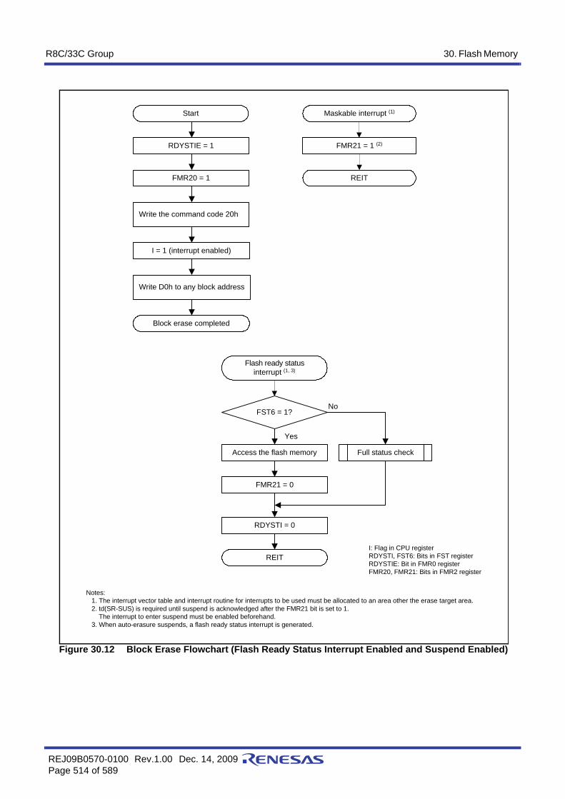
R8C/33C Group 30. Flash Memory
REJ09B0570-0100 Rev.1.00 Dec. 14, 2009Page 514 of 589
Figure 30.12 Block Erase Flowchart (Flash Ready Status Interrupt Enabled and Suspend Enabled)
Start
Write the command code 20h
Write D0h to any block address
I = 1 (interrupt enabled)
Block erase completed
RDYSTIE = 1
Maskable interrupt (1)
Notes: 1. The interrupt vector table and interrupt routine for interrupts to be used must be allocated to an area other the erase target area. 2. td(SR-SUS) is required until suspend is acknowledged after the FMR21 bit is set to 1. The interrupt to enter suspend must be enabled beforehand. 3. When auto-erasure suspends, a flash ready status interrupt is generated.
REIT
FMR21 = 1 (2)
Flash ready statusinterrupt (1, 3)
REIT
Access the flash memory
RDYSTI = 0
FMR21 = 0
FST6 = 1?
Yes
No
FMR20 = 1
I: Flag in CPU registerRDYSTI, FST6: Bits in FST registerRDYSTIE: Bit in FMR0 registerFMR20, FMR21: Bits in FMR2 register
Full status check

R8C/33C Group 30. Flash Memory
REJ09B0570-0100 Rev.1.00 Dec. 14, 2009Page 515 of 589
30.4.11.5 Lock Bit Program CommandThis command is used to set the lock bit of any block in the program ROM area to 0 (locked).When 77h is written in the first bus cycle and D0h is written in the second bus cycle to the starting blockaddress, 0 is written to the lock bit of the specified block. Make sure the address value in the first bus cycle isthe same address as the starting block address specified in the second bus cycle. Figure 30.13 shows a Lock Bit Program Flowchart. The lock bit status (lock bit data) can be read using the readlock bit status command. The FST7 bit in the FST register can be used to confirm whether writing to the lock bit has completed. Refer to 30.4.10 Data Protect Function for the lock bit function and how to set the lock bit to 1 (not locked).
Figure 30.13 Lock Bit Program Flowchart
Start
Write the command code 77h
Write D0h to the startingblock address
FST7 = 1?
Completed
No
Yes
FST7: Bit in FST register
Full status check

R8C/33C Group 30. Flash Memory
REJ09B0570-0100 Rev.1.00 Dec. 14, 2009Page 516 of 589
30.4.11.6 Read Lock Bit Status CommandThis command is used to read the lock bit status of any address in the program ROM area. When 71h written in the first bus cycle and D0h is written in the second cycle to the starting block address, thelock bit status of the specified block is stored in the LBDATA bit in the FST register. After the FST7 bit in theFST register has been set to 1 (ready), read the LBDATA bit.Figure 30.14 shows a Read Lock Bit Status Flowchart.
Figure 30.14 Read Lock Bit Status Flowchart
Start
Write D0h to the startingblock address
No
Write the command code 71h
FST7 = 1?
Yes
CompletedFST7: Bit in FST register
Full status check
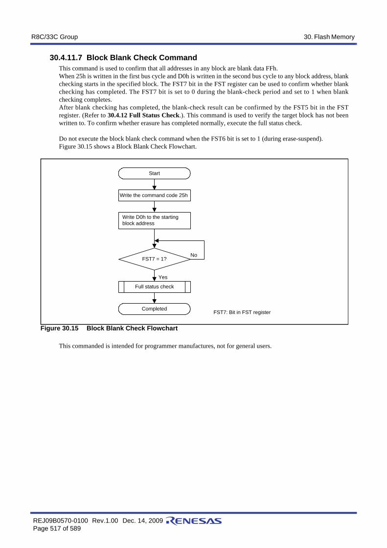
R8C/33C Group 30. Flash Memory
REJ09B0570-0100 Rev.1.00 Dec. 14, 2009Page 517 of 589
30.4.11.7 Block Blank Check CommandThis command is used to confirm that all addresses in any block are blank data FFh. When 25h is written in the first bus cycle and D0h is written in the second bus cycle to any block address, blankchecking starts in the specified block. The FST7 bit in the FST register can be used to confirm whether blankchecking has completed. The FST7 bit is set to 0 during the blank-check period and set to 1 when blankchecking completes. After blank checking has completed, the blank-check result can be confirmed by the FST5 bit in the FSTregister. (Refer to 30.4.12 Full Status Check.). This command is used to verify the target block has not beenwritten to. To confirm whether erasure has completed normally, execute the full status check.
Do not execute the block blank check command when the FST6 bit is set to 1 (during erase-suspend).Figure 30.15 shows a Block Blank Check Flowchart.
Figure 30.15 Block Blank Check Flowchart
This commanded is intended for programmer manufactures, not for general users.
Start
Write D0h to the startingblock address
No
Write the command code 25h
FST7 = 1?
Yes
CompletedFST7: Bit in FST register
Full status check

R8C/33C Group 30. Flash Memory
REJ09B0570-0100 Rev.1.00 Dec. 14, 2009Page 518 of 589
30.4.12 Full Status CheckIf an error occurs, bits FST4 and FST5 in the FST register are set to 1, indicating the occurrence of an error. Theexecution result can be confirmed by checking these status bits (full status check). Table 30.6 lists the Errors and FST Register Status. Figure 30.16 shows the Full Status Check and HandlingProcedure for Individual Errors.
Note:1. When FFh is written in the second bus cycle of these commands, the MCU enters read array mode.
At the same time, the command code written in the first bus cycle is invalid.
Table 30.6 Errors and FST Register StatusFST Register Status
Error Error Occurrence ConditionFST5 FST4
1 1 Command sequence error
• When a command is not written correctly.• When data other than valid data (i.e., D0h or FFh) is
written in the second bus cycle of the block erase command (1).
• The erase command is executed during suspend• The command is executed to the block during suspend
1 0 Erase error When the block erase command is executed, but auto-erasure does not complete correctly.
Blank check error When the block blank check command is executed and data other than blank data FFh is read.
0 1 Program error/lock bit program error
When the program command is executed, but auto-programming does not complete correctly.

R8C/33C Group 30. Flash Memory
REJ09B0570-0100 Rev.1.00 Dec. 14, 2009Page 519 of 589
Figure 30.16 Full Status Check and Handling Procedure for Individual Errors
Note: 1. To rewrite to the address where the program error occurs, ensure that
the full status check completes normally and write to the address after the block erase command is executed.
Full status check
FST4 = 1and
FST5 = 1?
FST5 = 1?
FST4 = 1?
Full status check completed
No
Yes
Yes
No
Yes
No
Command sequence error
Erase error/blank check error
Program error
Command sequence error
Execute the clear status register command(Set bits FST4 and FST5
in the FST register to 0)
Check if the command is properly input
Re-execute the command
Erase error/blank check error
Execute the clear status register command(Set bits FST4 and FST5
in the FST register to 0)
Erase commandRe-execution times ≤ 3 times?
Re-execute the block erase command
Program error
Execute the clear status register command(Set bits FST4 and FST5
in the FST register to 0)
Specify an address other than the writeaddress where the error occurs (1)
as the program address
Re-execute the program command
The erasure target blockcannot be used
No
Yes
FST4, FST5: Bits in FST registerFMR13: Bits in FMR1 register
Is the lock bit disabled?or
Is the command executed onthe data flash area?
No
Yes
Set FMR13 bit to 1
Is the lock bit disabled?or
Is the command executed onthe data flash area?
No
Yes
Set FMR13 bit to 1

R8C/33C Group 30. Flash Memory
REJ09B0570-0100 Rev.1.00 Dec. 14, 2009Page 520 of 589
30.5 Standard Serial I/O ModeIn standard serial I/O mode, a serial programmer which supports the MCU can be used to rewrite the user ROMarea while the MCU is mounted on-board. There are three types of standard serial I/O modes:• Standard serial I/O mode 1 .................Clock synchronous serial I/O used to connect to a serial programmer• Standard serial I/O mode 2 .................Clock asynchronous serial I/O used to connect to a serial programmer• Standard serial I/O mode 3 .................Special clock asynchronous serial I/O used to connect to a serial
programmer
Standard serial I/O mode 2 and standard serial I/O mode 3 can be used for the MCU.
Refer to Appendix 2. Connection Examples between Serial Writer and On-Chip Debugging Emulator forexamples of connecting to a serial programmer. Contact the serial programmer manufacturer for more information.Refer to the user’s manual included with your serial programmer for instructions.
Table 30.7 lists the Pin Functions (Flash Memory Standard Serial I/O Mode 2) and Figure 30.17 shows PinHandling in Standard Serial I/O Mode 2. Table 30.8 lists the Pin Functions (Flash Memory Standard Serial I/OMode 3) and Figure 30.18 shows Pin Handling in Standard Serial I/O Mode 3.After handling the pins shown in Table 30.8 and rewriting the flash memory using the programmer, apply a “H”level signal to the MODE pin and reset the hardware to run a program in the flash memory in single-chip mode.
30.5.1 ID Code Check FunctionThe ID code check function determines whether the ID codes sent from the serial programmer and those writtenin the flash memory match.Refer to 12. ID Code Areas for details of the ID code check.

R8C/33C Group 30. Flash Memory
REJ09B0570-0100 Rev.1.00 Dec. 14, 2009Page 521 of 589
I: Input O: Output I/O: Input and output
Figure 30.17 Pin Handling in Standard Serial I/O Mode 2
Table 30.7 Pin Functions (Flash Memory Standard Serial I/O Mode 2)Pin Name I/O Description
VCC, VSS Power supply input Apply the guaranteed programming and erasure voltage to the VCC pin and 0 V to the VSS pin.
RESET Reset input I Reset input pinP4_6/XIN/(XCIN) P4_6 input/clock input I Connect a ceramic resonator or crystal oscillator
between pins XIN(XCIN) and XOUT(XCOUT). P4_7/XOUT/(XCOUT) P4_7 input/clock output I/OP0_0 to P0_7 Input port P0 I Input a “H” or “L” level signal or leave open.P1_0 to P1_3, P1_6, P1_7
Input port P1 I Input a “H” or “L” level signal or leave open.
P2_0 to P2_2 Input port P2 I Input a “H” or “L” level signal or leave open.P3_1, P3_3 to P3_5, P3_7
Input port P3 I Input a “H” or “L” level signal or leave open.
P4_2/VREF, P4_5 Input port P4 I Input a “H” or “L” level signal or leave open.MODE MODE I/O Input a “L” level signal.P1_4 TXD output O Serial data output pin P1_5 RXD input I Serial data input pin
Notes:1. In this example, modes are switched between single-chip mode and standard serial I/O mode
by controlling the MODE input with a switch.2. When operating with the on-chip oscillator clock, it is not necessary to connect an oscillation
circuit. Refer to Appendix Figure 2.1 Connection Example with M16C Flash Starter (M3A-0806).
MCU
TXD
RXD
Data output
Data input
MODE
VCC
AVCC
VSS
AVSS
RESETUser reset signal
Connect an oscillator (2)
XIN/(XCIN )
XOUT/(XCOUT)

R8C/33C Group 30. Flash Memory
REJ09B0570-0100 Rev.1.00 Dec. 14, 2009Page 522 of 589
I: Input O: Output I/O: Input and output
Figure 30.18 Pin Handling in Standard Serial I/O Mode 3
Table 30.8 Pin Functions (Flash Memory Standard Serial I/O Mode 3)Pin Name I/O Description
VCC, VSS Power supply input Apply the guaranteed programming and erasure voltage to the VCC pin and 0 V to the VSS pin.
RESET Reset input I Reset input pinP4_6/XIN/(XCIN) P4_6 input/clock input I If an external oscillator is connected, connect a
ceramic resonator or crystal oscillator between pins XIN(XCIN) and XOUT(XCOUT). To use as an input port, input a “H” or “L” level signal or leave the pin open.
P4_7/XOUT/(XCOUT) P4_7 input/clock output I/O
P0_0 to P0_7 Input port P0 I Input a “H” or “L” level signal or leave open.P1_0 to P1_7 Input port P1 I Input a “H” or “L” level signal or leave open.P2_0 to P2_2 Input port P2 I Input a “H” or “L” level signal or leave open.P3_1, P3_3 to P3_5, P3_7
Input port P3 I Input a “H” or “L” level signal or leave open.
P4_2/VREF, P4_5 Input port P4 I Input a “H” or “L” level signal or leave open.MODE MODE I/O Serial data I/O pin. Connect the pin to a
programmer.
Notes:1. Controlled pins and external circuits vary depending on the programmer.
Refer to the programmer manual for details.2. In this example, modes are switched between single-chip mode and
standard serial I/O mode by connecting a programmer.3. When operating with the on-chip oscillator clock, it is not necessary to
connect an oscillation circuit.
MCU
MODE
RESET
MODE I/O
Reset input
User reset signalVSS
AVSS
VCC
AVCC

R8C/33C Group 30. Flash Memory
REJ09B0570-0100 Rev.1.00 Dec. 14, 2009Page 523 of 589
30.6 Parallel I/O ModeParallel I/O mode is used to input and output software commands, addresses and data necessary to control (read,program, and erase) the on-chip flash memory. Use a parallel programmer which supports the MCU. Contact the parallel programmer manufacturer for moreinformation. Refer to the user’s manual included with your parallel programmer for instructions.In parallel I/O mode, the user ROM areas shown in Figure 30.1 can be rewritten.
30.6.1 ROM Code Protect FunctionThe ROM code protect function prevents the flash memory from being read and rewritten. (Refer to the 30.3.2ROM Code Protect Function.)

R8C/33C Group 30. Flash Memory
REJ09B0570-0100 Rev.1.00 Dec. 14, 2009Page 524 of 589
30.7 Notes on Flash Memory
30.7.1 CPU Rewrite Mode
30.7.1.1 Prohibited InstructionsThe following instructions cannot be used while the program ROM area is being rewritten in EW0 modebecause they reference data in the flash memory: UND, INTO, and BRK.
30.7.1.2 InterruptsTables 30.9 and 30.11 show CPU Rewrite Mode Interrupts (1), (2) and (3), respectively.
FMR21, FMR22: Bits in FMR2 register
Table 30.9 CPU Rewrite Mode Interrupts (1)
ModeErase/Write Target
Status Maskable Interrupt
EW0 Data flash
During auto-erasure(suspend enabled)
When an interrupt request is acknowledged, interrupt handling is executed. If the FMR22 bit is set to 1 (erase-suspend request enabled by interrupt request), the FMR21 bit is automatically set to 1 (erase-suspend request). The flash memory suspends auto-erasure after td(SR-SUS). If erase-suspend is required while the FMR22 bit is set to 0 (erase-suspend request disabled by interrupt request), set the FMR21 bit to 1 during interrupt handling. The flash memory suspends auto-erasure after td(SR-SUS).While auto-erasure is being suspended, any block other than the block during auto-erasure execution can be read or written. Auto-erasure can be restarted by setting the FMR21 bit to 0 (erase restart).
During auto-erasure(suspend disabled or FMR22 = 0)
Interrupt handling is executed while auto-erasure or auto-programming is being performed.
During auto-programming
Program ROM
During auto-erasure(suspend enabled)
Usable by allocating a vector in RAM.
During auto-erasure(suspend disabled)During auto-programming
EW1 Data flash
During auto-erasure(suspend enabled)
When an interrupt request is acknowledged, interrupt handling is executed. If the FMR22 bit is set to 1, the FMR21 bit is automatically set to 1. The flash memory suspends auto-erasure after td(SR-SUS). If erase-suspend is required while the FMR22 bit is set to 0, set the FMR21 bit to 1 during interrupt handling. The flash memory suspends auto-erasure after td(SR-SUS).While auto-erasure is being suspended, any block other than the block during auto-erasure execution can be read or written. Auto-erasure can be restarted by setting the FMR21 bit to 0.
During auto-erasure(suspend disabled or FMR22 = 0)
Interrupt handling is executed while auto-erasure or auto-programming is being performed.
During auto-programming
Program ROM
During auto-erasure(suspend enabled)
Auto-erasure suspends after td(SR-SUS) and interrupt handling is executed. Auto-erasure can be restarted by setting the FMR21 bit to 0 after interrupt handling completes. While auto-erasure is being suspended, any block other than the block during auto-erasure execution can be read or written.
During auto-erasure(suspend disabled or FMR22 = 0)
Auto-erasure and auto-programming have priority and interrupt requests are put on standby. Interrupt handling is executed after auto-erase and auto-program complete.
During auto-programming

R8C/33C Group 30. Flash Memory
REJ09B0570-0100 Rev.1.00 Dec. 14, 2009Page 525 of 589
FMR21, FMR22: Bits in FMR2 registerNote:
1. Do not use a non-maskable interrupt while block 0 is being auto-erased because the fixed vector is allocated in block 0.
Table 30.10 CPU Rewrite Mode Interrupts (2)
ModeErase/Write Target
Status
• Watchdog Timer• Oscillation Stop Detection• Voltage Monitor 2• Voltage Monitor 1• NMI (Note 1)
• Undefined Instruction• INTO Instruction• BRK Instruction• Single Step• Address Match• Address Break (Note 1)
EW0 Data flash During auto-erasure(suspend enabled)
When an interrupt request is acknowledged, interrupt handling is executed. If the FMR22 bit is set to 1 (erase-suspend request enabled by interrupt request), the FMR21 bit is automatically set to 1 (erase-suspend request). The flash memory suspends auto-erasure after td(SR-SUS). If erase-suspend is required while the FMR22 bit is set to 0 (erase-suspend request disabled by interrupt request), set the FMR21 bit to 1 during interrupt handling. The flash memory suspends auto-erasure after td(SR-SUS).While auto-erasure is being suspended, any block other than the block during auto-erasure execution can be read or written. Auto-erasure can be restarted by setting the FMR21 bit is set to 0 (erase restart).
When an interrupt request is acknowledged, interrupt handling is executed.If erase-suspend is required, set the FMR21 bit to 1 during interrupt handling. The flash memory suspends auto-erasure after td(SR-SUS).While auto-erasure is being suspended, any block other than the block during auto-erasure execution can be read or written. Auto-erasure can be restarted by setting the FMR21 bit in the FMR2 register is set to 0 (erase restart).
During auto-erasure(suspend disabled or FMR22 = 0)
Interrupt handling is executed while auto-erasure or auto-programming is being performed.
During auto-programming
Program ROM
During auto-erasure(suspend enabled)
When an interrupt request is acknowledged, auto-erasure or auto-programming is forcibly stopped immediately and the flash memory is reset. Interrupt handling starts when the flash memory restarts after the fixed period. Since the block during auto-erasure or the address during auto-programming is forcibly stopped, the normal value may not be read. After the flash memory restarts, execute auto-erasure again and ensure it completes normally. The watchdog timer does not stop during the command operation, so interrupt requests may be generated. Initialize the watchdog timer regularly using the erase-suspend function.
Not usable during auto-erasure or auto-programming.
During auto-erasure(suspend disabled)During auto-programming

R8C/33C Group 30. Flash Memory
REJ09B0570-0100 Rev.1.00 Dec. 14, 2009Page 526 of 589
FMR21, FMR22: Bits in FMR2 registerNote:
1. Do not use a non-maskable interrupt while block 0 is being auto-erased because the fixed vector is allocated in block 0.
Table 30.11 CPU Rewrite Mode Interrupts (3)
ModeErase/Write Target
Status
• Watchdog Timer• Oscillation Stop Detection• Voltage Monitor 2• Voltage Monitor 1• NMI (Note 1)
• Undefined Instruction• INTO Instruction• BRK Instruction• Single Step• Address Match• Address Break (Note 1)
EW1 Data flash During auto-erasure(suspend enabled)
When an interrupt request is acknowledged, interrupt handling is executed. If the FMR22 bit is set to 1, the FMR21 bit is automatically set to 1. The flash memory suspends auto-erasure after td(SR-SUS). If erase-suspend is required while the FMR22 bit is set to 0, set the FMR21 bit to 1 during interrupt handling. The flash memory suspends auto-programming after td(SR-SUS).While auto-erasure is being suspended, any block other than the block during auto-erasure execution can be read or written. Auto-erasure can be restarted by setting the FMR21 bit is set to 0.
When an interrupt request is acknowledged, interrupt handling is executed.If erase-suspend is required, set the FMR21 bit to 1 during interrupt handling. The flash memory suspends auto-erasure after td(SR-SUS).While auto-erasure is being suspended, any block other than the block during auto-erasure execution can be read or written. Auto-erasure can be restarted by setting the FMR21 bit in the FMR2 register is set to 0 (erase restart).
During auto-erasure(suspend disabled or FMR22 = 0)
Interrupt handling is executed while auto-erasure or auto-programming is being performed.
During auto-programming
Program ROM
During auto-erasure(suspend enabled)
When an interrupt request is acknowledged, auto-erasure or auto-programming is forcibly stopped immediately and the flash memory is reset. Interrupt handling starts when the flash memory restarts after the fixed period. Since the block during auto-erasure or the address during auto-programming is forcibly stopped, the normal value may not be read. After the flash memory restarts, execute auto-erasure again and ensure it completes normally. The watchdog timer does not stop during the command operation, so interrupt requests may be generated. Initialize the watchdog timer regularly using the erase-suspend function.
Not usable during auto-erasure orauto-programming.
During auto-erasure(suspend disabled or FMR22 = 0)During auto-programming

R8C/33C Group 30. Flash Memory
REJ09B0570-0100 Rev.1.00 Dec. 14, 2009Page 527 of 589
30.7.1.3 How to AccessTo set one of the following bits to 1, first write 0 and then 1 immediately. Disable interrupts and DTC activationbetween writing 0 and writing 1.• The FMR01 bit or FMR02 bit in the FMR0 register• The FMR13 bit in the FMR1 register• The FMR20 bit, FMR22 bit, or FMR 27 bit in the FMR2 register
To set one of the following bits to 0, first write 1 and then 0 immediately. Disable interrupts and DTC activationbetween writing 0 and writing 1.• The FMR14 bit, FMR15 bit, FMR16 bit, or FMR17 bit in the FMR1 register
30.7.1.4 Rewriting User ROM AreaIn EW0 Mode, if the supply voltage drops while rewriting any block in which a rewrite control program isstored, it may not be possible to rewrite the flash memory because the rewrite control program cannot berewritten correctly. In this case, use standard serial I/O mode.
30.7.1.5 ProgrammingDo not write additions to the already programmed address.
30.7.1.6 Entering Stop Mode or Wait ModeDo not enter stop mode or wait mode during erase-suspend.If the FST7 in the FST register is set to 0 (busy (during programming or erasure execution)), do not enter to stopmode or wait mode.Do not enter stop mode or wait mode while the FMR27 bit is 1 (low-current-consumption read mode enabled).
30.7.1.7 Programming and Erasure Voltage for Flash MemoryTo perform programming and erasure, use VCC = 2.7 V to 5.5 V as the supply voltage. Do not performprogramming and erasure at less than 2.7 V.
30.7.1.8 Block Blank CheckDo not execute the block blank check command during erase-suspend.
30.7.1.9 Low-Current-Consumption Read ModeIn low-speed clock mode and low-speed on-chip oscillator mode, the current consumption when reading theflash memory can be reduced by setting the FMR27 bit in the FMR2 register to 1 (low-current-consumptionread mode enabled).Low-current-consumption read mode can be used when the CPU clock is set to either of the following:• The CPU clock is set to the low-speed on-chip oscillator clock divided by 4, 8, or 16.• The CPU clock is set to the XCIN clock divided by 1 (no division), 2, 4, or 8.However, do not use low-current-consumption read mode when the frequency of the selected CPU clock is3 kHz or below. After setting the divide ratio of the CPU clock, set the FMR27 bit to 1 (low-current-consumption read mode enabled).To reduce the power consumption, refer to 31. Reducing Power Consumption.Enter wait mode or stop mode after setting the FMR27 bit to 0 (low-current-consumption read mode disabled).Do not enter wait mode or stop mode while the FMR27 bit is 1 (low-current-consumption read mode enabled).

R8C/33C Group 31. Reducing Power Consumption
REJ09B0570-0100 Rev.1.00 Dec. 14, 2009Page 528 of 589
31. Reducing Power Consumption
31.1 OverviewThis chapter describes key points and processing methods for reducing power consumption.
31.2 Key Points and Processing Methods for Reducing Power ConsumptionKey points for reducing power consumption are shown below. They should be referred to when designing a systemor creating a program.
31.2.1 Voltage Detection CircuitIf voltage monitor 1 is not used, set the VCA26 bit in the VCA2 register to 0 (voltage detection 1 circuitdisabled). If voltage monitor 2 is not used, set the VCA27 bit in the VCA2 register to 0 (voltage detection 2circuit disabled).If the power-on reset and voltage monitor 0 reset are not used, set the VCA25 bit in the VCA2 register to 0(voltage detection 0 circuit disabled).
31.2.2 PortsEven after the MCU enters wait mode or stop mode, the states of the I/O ports are retained. Current flows intothe output ports in the active state, and shoot-through current flows into the input ports in the high-impedancestate. Unnecessary ports should be set to input and fixed to a stable electric potential before the MCU enterswait mode or stop mode.
31.2.3 ClocksPower consumption generally depends on the number of the operating clocks and their frequencies. The fewerthe number of operating clocks or the lower their frequencies, the more power consumption decreases. Unnecessary clocks should be stopped accordingly.
Stopping low-speed on-chip oscillator oscillation: CM14 bit in CM1 registerStopping high-speed on-chip oscillator oscillation: FRA00 bit in FRA0 register
31.2.4 Wait Mode, Stop ModePower consumption can be reduced in wait mode and stop mode. Refer to 9.7 Power Control for details.
31.2.5 Stopping Peripheral Function ClocksIf the peripheral function f1, f2, f4, f8, and f32 clocks are not necessary in wait mode, set the CM02 bit in theCM0 register to 1 (peripheral function clock stops in wait mode). This will stop the f1, f2, f4, f8, and f32 clocksin wait mode.
31.2.6 TimersIf timer RA is not used, set the TCKCUT bit in the TRAMR register to 1 (count source cutoff).If timer RB is not used, set the TCKCUT bit in the TRBMR register to 1 (count source cutoff).If timer RC is not used, set the MSTTRC bit in the MSTCR register to 1 (standby).
31.2.7 A/D ConverterWhen the A/D converter is not used, power consumption can be reduced by setting the ADSTBY bit in theADCON1 register to 0 (A/D operation stops (standby)) to shut off any analog circuit current flow.
31.2.8 Clock Synchronous Serial InterfaceWhen the SSU or the I2C bus is not used, set the MSTIIC bit in the MSTCR register to 1 (standby).

R8C/33C Group 31. Reducing Power Consumption
REJ09B0570-0100 Rev.1.00 Dec. 14, 2009Page 529 of 589
31.2.9 Reducing Internal Power ConsumptionWhen the MCU enters wait mode using low-speed clock mode or low-speed on-chip oscillator mode, internalpower consumption can be reduced by using the VCA20 bit in the VCA2 register. Figure 31.1 shows theHandling Procedure for Reducing Internal Power Consumption Using VCA20 Bit. To enable reduced internalpower consumption by the VCA20 bit, follow Figure 31.1 Handling Procedure for Reducing Internal PowerConsumption Using VCA20 Bit.
Figure 31.1 Handling Procedure for Reducing Internal Power Consumption Using VCA20 Bit
Notes:1. Execute this routine to handle all interrupts generated in wait mode.
However, this does not apply if it is not necessary to start the high-speed clock or high-speed on-chip oscillator during the interrupt routine.2. Do not set the VCA20 bit to 0 with the instruction immediately after setting the VCA20 bit to 1. Also, do not do the opposite.3. When the VCA20 bit is set to 1, do not set the CM10 bit to 1 (stop mode).4. When the MCU enters wait mode, follow 9.7.2 Wait Mode.
Procedure for enabling reduced internalpower consumption using VCA20 bit
Enter low-speed clock mode orlow-speed on-chip oscillator mode
Stop XIN clock andhigh-speed on-chip oscillator clock
VCA20 ← 1(internal power low consumption enabled) (2, 3)
Enter wait mode (4)
VCA20 ← 0(internal power low consumption disabled) (2)
Start XIN clock orhigh-speed on-chip oscillator clock
(Wait until XIN clock or high-speed on-chiposcillator clock oscillation stabilizes)
Enter high-speed clock mode orhigh-speed on-chip oscillator mode
In interrupt routine
VCA20 ← 0(internal power low consumption disabled) (2)
(This is automatically set when exiting wait mode)
Start XIN clockor high-speed on-chip oscillator clock
Enter high-speed clock mode orhigh-speed on-chip oscillator mode
Enter low-speed clock mode orlow-speed on-chip oscillator mode
Exit wait mode by interrupt
Stop XIN clock andhigh-speed on-chip oscillator clock
VCA20 ← 1(internal power low consumption enabled) (2, 3)
Interrupt handling completed
Step (1)
Step (2)
Step (3)
Step (4)
Step (5)
Step (6)
Step (7)
Step (8)
Step (5)
Step (6)
Step (7)
Step (8)
(Wait until XIN clock or high-speed on-chiposcillator clock oscillation stabilizes)
Step (1)
Step (2)
Step (3)
If it is necessary to startthe high-speed clock orhigh-speed on-chip oscillatorduring the interrupt routine,execute steps (6) to (7)in the routine.
If the high-speed clock orhigh-speed on-chip oscillatorstarts during the interruptroutine, execute steps (1) to(3) at the end of the routine.
(Note 1)
Interrupt handling
VCA20: Bit in VCA2 register

R8C/33C Group 31. Reducing Power Consumption
REJ09B0570-0100 Rev.1.00 Dec. 14, 2009Page 530 of 589
31.2.10 Stopping Flash MemoryIn low-speed on-chip oscillator mode and low-speed clock mode, power consumption can be further reduced bystopping the flash memory using the FMSTP bit in the FMR0 register.Access to the flash memory is disabled by setting the FMSTP bit to 1 (flash memory stops). The FMSTP bitmust be written to by a program transferred to RAM.When the MCU enters stop mode or wait mode while CPU rewrite mode is disabled, the power for the flashmemory is automatically turned off. It is turned back on again after the MCU exit stop mode or wait mode. Thiseliminates the need to set the FMR0 register. Figure 31.2 shows the Handling Procedure Example for Reducing Power Consumption Using FMSTP Bit.
Figure 31.2 Handling Procedure Example for Reducing Power Consumption Using FMSTP Bit
FMSTP bit setting program
Transfer the FMSTP bit setting program tothe RAM
Jump to the FMSTP bit setting program(The subsequent processing is executedby the program in the RAM)
After writing 0 to the FMR01 bit,write 1 (CPU rewrite mode enabled)
Enter low-speed clock mode orlow-speed on-chip oscillator mode
Process in low-speed clock mode orlow-speed on-chip oscillator mode
Write 0 to the FMR01 bit(CPU rewrite mode disabled)
Jump to the specified address in the flash memory
Notes:1. After setting the FMR01 bit to 1 (CPU rewrite mode enabled), set the FMSTP bit to 1 (flash memory stops).
2. Before switching the CPU clock source, make sure the designated clock is stable. 3. Insert a 60-µs wait time by a program. Do not access the flash memory during this wait time.
Write 1 to the FMSTP bit (flash memory stops.low power consumption state) (1)
Wait until the flash memory circuit stabilizes(60 µs) (3)
Write 0 to the FMSTP bit(flash memory operates)
Switch the clock source for the CPU clock (2)
FMR01, FMSTP: Bits in FMR0 register
Stop the high-speed on-chip oscillator

R8C/33C Group 31. Reducing Power Consumption
REJ09B0570-0100 Rev.1.00 Dec. 14, 2009Page 531 of 589
31.2.11 Low-Current-Consumption Read ModeIn low-speed clock mode and low-speed on-chip oscillator mode, the current consumption when reading theflash memory can be reduced by setting the FMR27 bit in the FMR2 register to 1 (low-current-consumptionread mode enabled).Low-current-consumption read mode can be used when the CPU clock is set to either of the following:• The CPU clock is set to the low-speed on-chip oscillator clock divided by 4, 8, or 16.• The CPU clock is set to the XCIN clock divided by 1 (no division), 2, 4, or 8.However, do not use low-current-consumption read mode when the frequency of the selected CPU clock is3 kHz or below. After setting the divide ratio of the CPU clock, set the FMR27 bit to 1 (low-current-consumption read modeenabled).Enter wait mode or stop mode after setting the FMR27 bit to 0 (low-current-consumption read mode disabled).Do not enter wait mode or stop mode while the FMR27 bit is 1 (low-current-consumption read mode enabled).Figure 31.3 shows the Handling Procedure Example of Low-Current-Consumption Read Mode.
Figure 31.3 Handling Procedure Example of Low-Current-Consumption Read Mode
Notes:1. To set the FMR27 bit to 1, first write 0 and then write 1 immediately.
Disable interrupts and DTC activation between writing 0 and writing 1.2. In low-current-consumption read mode, set the FMR01 bit in the FMR0 register to 0 (CPU rewrite mode disabled).
Enter wait mode or stop mode after setting the FMR27 bit to 0 (low-current-consumption read mode disabled).Do not enter wait mode or stop mode while the FMR27 bit is 1 (low-current-consumption read mode enabled).
Handling procedure for enablinglow-current-consumption read mode
by FMR27 bit
Step (1)
Step (2)
Step (3)
Step (4)
Step (5)
Step (6)
Step (7)
Step (8)
FMR27: Bit in FMR2 register
Enter low-speed clock mode orlow-speed on-chip oscillator mode
Stop the high-speed on-chip oscillator clock
FMR27 ← 1(low-current-consumption read mode enabled) (1)
Enter low-current-consumption read mode (2)
FMR27 ← 0(low-current-consumption read mode disabled)
Start the high-speed on-chip oscillator clock
(Wait until the high-speed on-chip oscillator clockoscillation stabilizes)
Enter high-speed on-chip oscillator mode

R8C/33C Group 31. Reducing Power Consumption
REJ09B0570-0100 Rev.1.00 Dec. 14, 2009Page 532 of 589
31.2.12 OthersSet the MSTTRD bit in the MSTCR register to 1.The power consumption of the peripheral functions can be reduced.

R8C/33C Group 32. Electrical Characteristics
REJ09B0570-0100 Rev.1.00 Dec. 14, 2009Page 533 of 589
32. Electrical Characteristics
Table 32.1 Absolute Maximum RatingsSymbol Parameter Condition Rated Value Unit
VCC/AVCC Supply voltage −0.3 to 6.5 VVI Input voltage −0.3 to VCC + 0.3 VVO Output voltage −0.3 to VCC + 0.3 VPd Power dissipation −40°C ≤ Topr ≤ 85°C 500 mWTopr Operating ambient temperature −20 to 85 (N version) /
−40 to 85 (D version)°C
Tstg Storage temperature −65 to 150 °C

R8C/33C Group 32. Electrical Characteristics
REJ09B0570-0100 Rev.1.00 Dec. 14, 2009Page 534 of 589
Notes:1. VCC = 1.8 to 5.5 V and Topr = −20 to 85°C (N version) / −40 to 85°C (D version), unless otherwise specified.2. The average output current indicates the average value of current measured during 100 ms.3. fOCO40M can be used as the count source for timer RC in the range of VCC = 2.7 V to 5.5 V.
Table 32.2 Recommended Operating Conditions
Symbol Parameter ConditionsStandard
UnitMin. Typ. Max.
VCC/AVCC Supply voltage 1.8 − 5.5 VVSS/AVSS Supply voltage − 0 − VVIH Input “H” voltage Other than CMOS input 0.8 VCC − VCC V
CMOS input
Input level switching function (I/O port)
Input level selection: 0.35 VCC
4.0 V ≤ VCC ≤ 5.5 V 0.5 VCC − VCC V2.7 V ≤ VCC < 4.0 V 0.55 VCC − VCC V1.8 V ≤ VCC < 2.7 V 0.65 VCC − VCC V
Input level selection: 0.5 VCC
4.0 V ≤ VCC ≤ 5.5 V 0.65 VCC − VCC V2.7 V ≤ VCC < 4.0 V 0.7 VCC − VCC V1.8 V ≤ VCC < 2.7 V 0.8 VCC − VCC V
Input level selection: 0.7 VCC
4.0 V ≤ VCC ≤ 5.5 V 0.85 VCC − VCC V2.7 V ≤ VCC < 4.0 V 0.85 VCC − VCC V1.8 V ≤ VCC < 2.7 V 0.85 VCC − VCC V
External clock input (XOUT) 1.2 − VCC VVIL Input “L” voltage Other than CMOS input 0 − 0.2 VCC V
CMOS input
Input level switching function (I/O port)
Input level selection: 0.35 VCC
4.0 V ≤ VCC ≤ 5.5 V 0 − 0.2 VCC V2.7 V ≤ VCC < 4.0 V 0 − 0.2 VCC V1.8 V ≤ VCC < 2.7 V 0 − 0.2 VCC V
Input level selection: 0.5 VCC
4.0 V ≤ VCC ≤ 5.5 V 0 − 0.4 VCC V2.7 V ≤ VCC < 4.0 V 0 − 0.3 VCC V1.8 V ≤ VCC < 2.7 V 0 − 0.2 VCC V
Input level selection: 0.7 VCC
4.0 V ≤ VCC ≤ 5.5 V 0 − 0.55 VCC V2.7 V ≤ VCC < 4.0 V 0 − 0.45 VCC V1.8 V ≤ VCC < 2.7 V 0 − 0.35 VCC V
External clock input (XOUT) 0 − 0.4 VIOH(sum) Peak sum output
“H” currentSum of all pins IOH(peak) − − −160 mA
IOH(sum) Average sum output “H” current
Sum of all pins IOH(avg) − − −80 mA
IOH(peak) Peak output “H” current
Drive capacity Low − − −10 mADrive capacity High − − −40 mA
IOH(avg) Average output “H” current
Drive capacity Low − − −5 mADrive capacity High − − −20 mA
IOL(sum) Peak sum output “L” current
Sum of all pins IOL(peak) − − 160 mA
IOL(sum) Average sum output “L” current
Sum of all pins IOL(avg) − − 80 mA
IOL(peak) Peak output “L” current
Drive capacity Low − − 10 mADrive capacity High − − 40 mA
IOL(avg) Average output “L” current
Drive capacity Low − − 5 mADrive capacity High − − 20 mA
f(XIN) XIN clock input oscillation frequency 2.7 V ≤ VCC ≤ 5.5 V − − 20 MHz1.8 V ≤ VCC < 2.7 V − − 5 MHz
f(XCIN) XCIN clock input oscillation frequency 1.8 V ≤ VCC ≤ 5.5 V − 32.768 50 kHzfOCO40M When used as the count source for timer RC (3) 2.7 V ≤ VCC ≤ 5.5 V 32 − 40 MHzfOCO-F fOCO-F frequency 2.7 V ≤ VCC ≤ 5.5 V − − 20 MHz
1.8 V ≤ VCC < 2.7 V − − 5 MHz− System clock frequency 2.7 V ≤ VCC ≤ 5.5 V − − 20 MHz
1.8 V ≤ VCC < 2.7 V − − 5 MHzf(BCLK) CPU clock frequency 2.7 V ≤ VCC ≤ 5.5 V − − 20 MHz
1.8 V ≤ VCC < 2.7 V − − 5 MHz

R8C/33C Group 32. Electrical Characteristics
REJ09B0570-0100 Rev.1.00 Dec. 14, 2009Page 535 of 589
Figure 32.1 Ports P0 to P4 Timing Measurement Circuit
P0P1P2P3P4
30pF

R8C/33C Group 32. Electrical Characteristics
REJ09B0570-0100 Rev.1.00 Dec. 14, 2009Page 536 of 589
Notes:1. VCC/AVCC = Vref = 2.2 to 5.5 V, VSS = 0 V and Topr = −20 to 85°C (N version) / −40 to 85°C (D version), unless otherwise
specified.2. The A/D conversion result will be undefined in wait mode, stop mode, when the flash memory stops, and in low-current-
consumption mode. Do not perform A/D conversion in these states or transition to these states during A/D conversion.3. When the analog input voltage is over the reference voltage, the A/D conversion result will be 3FFh in 10-bit mode and FFh in
8-bit mode.
Table 32.3 A/D Converter Characteristics
Symbol Parameter ConditionsStandard
UnitMin. Typ. Max.
− Resolution Vref = AVCC − − 10 Bit− Absolute accuracy 10-bit mode Vref = AVCC = 5.0 V AN0 to AN7 input,
AN8 to AN11 input− − ±3 LSB
Vref = AVCC = 3.3 V AN0 to AN7 input, AN8 to AN11 input
− − ±5 LSB
Vref = AVCC = 3.0 V AN0 to AN7 input, AN8 to AN11 input
− − ±5 LSB
Vref = AVCC = 2.2 V AN0 to AN7 input, AN8 to AN11 input
− − ±5 LSB
8-bit mode Vref = AVCC = 5.0 V AN0 to AN7 input, AN8 to AN11 input
− − ±2 LSB
Vref = AVCC = 3.3 V AN0 to AN7 input, AN8 to AN11 input
− − ±2 LSB
Vref = AVCC = 3.0 V AN0 to AN7 input, AN8 to AN11 input
− − ±2 LSB
Vref = AVCC = 2.2 V AN0 to AN7 input, AN8 to AN11 input
− − ±2 LSB
φAD A/D conversion clock 4.0 ≤ Vref = AVCC ≤ 5.5 V (2) 2 − 20 MHz
3.2 ≤ Vref = AVCC ≤ 5.5 V (2) 2 − 16 MHz
2.7 ≤ Vref = AVCC ≤ 5.5 V (2) 2 − 10 MHz
2.2 ≤ Vref = AVCC ≤ 5.5 V (2) 2 − 5 MHz− Tolerance level impedance − 3 − kΩtCONV Conversion time 10-bit mode Vref = AVCC = 5.0 V, φAD = 20 MHz 2.15 − − µs
8-bit mode Vref = AVCC = 5.0 V, φAD = 20 MHz 2.15 − − µstSAMP Sampling time φAD = 20 MHz 0.75 − − µsIVref Vref current Vcc = 5 V, XIN = f1 = φAD = 20 MHz − 45 − µAVref Reference voltage 2.2 − AVCC VVIA Analog input voltage (3) 0 − Vref V

R8C/33C Group 32. Electrical Characteristics
REJ09B0570-0100 Rev.1.00 Dec. 14, 2009Page 537 of 589
Notes:1. VCC/AVCC = Vref = 2.7 to 5.5 V and Topr = −20 to 85°C (N version) / −40 to 85°C (D version), unless otherwise specified.2. This applies when one D/A converter is used and the value of the DAi register (i = 0 or 1) for the unused D/A converter is 00h.
The resistor ladder of the A/D converter is not included.
Notes:1. VCC = 2.7 to 5.5 V, Topr = −20 to 85°C (N version) / −40 to 85°C (D version), unless otherwise specified.2. When the digital filter is disabled.
Table 32.4 D/A Converter Characteristics
Symbol Parameter ConditionStandard
UnitMin. Typ. Max.
− Resolution − − 8 Bit− Absolute accuracy − − 2.5 LSBtsu Setup time − − 3 µsRO Output resistor − 6 − kΩIVref Reference power input current (Note 2) − − 1.5 mA
Table 32.5 Comparator B Electrical Characteristics
Symbol Parameter ConditionStandard
UnitMin. Typ. Max.
Vref IVREF1, IVREF3 input reference voltage 0 − VCC − 1.4 VVI IVCMP1, IVCMP3 input voltage −0.3 − VCC + 0.3 V− Offset − 5 100 mVtd Comparator output delay time (2) VI = Vref ± 100 mV − 0.1 − µsICMP Comparator operating current VCC = 5.0 V − 17.5 − µA

R8C/33C Group 32. Electrical Characteristics
REJ09B0570-0100 Rev.1.00 Dec. 14, 2009Page 538 of 589
Notes:1. VCC = 2.7 to 5.5 V and Topr = 0 to 60°C, unless otherwise specified.2. Definition of programming/erasure endurance
The programming and erasure endurance is defined on a per-block basis.If the programming and erasure endurance is n (n = 1,000), each block can be erased n times. For example, if 1,024 1-byte writes are performed to different addresses in block A, a 1 Kbyte block, and then the block is erased, the programming/erasure endurance still stands at one.However, the same address must not be programmed more than once per erase operation (overwriting prohibited).
3. Endurance to guarantee all electrical characteristics after program and erase. (1 to Min. value can be guaranteed).4. In a system that executes multiple programming operations, the actual erasure count can be reduced by writing to sequential
addresses in turn so that as much of the block as possible is used up before performing an erase operation. For example, when programming groups of 16 bytes, the effective number of rewrites can be minimized by programming up to 128 groups before erasing them all in one operation. It is also advisable to retain data on the erasure endurance of each block and limit the number of erase operations to a certain number.
5. If an error occurs during block erase, attempt to execute the clear status register command, then execute the block erase command at least three times until the erase error does not occur.
6. Customers desiring program/erase failure rate information should contact their Renesas technical support representative.7. The data hold time includes time that the power supply is off or the clock is not supplied.
Table 32.6 Flash Memory (Program ROM) Electrical Characteristics
Symbol Parameter ConditionsStandard
UnitMin. Typ. Max.
− Program/erase endurance (2) 1,000 (3) − − times− Byte program time − 80 500 µs− Block erase time − 0.3 − std(SR-SUS) Time delay from suspend request until
suspend− − 5+CPU clock
× 3 cyclesms
− Interval from erase start/restart until following suspend request
0 − − µs
− Time from suspend until erase restart − − 30+CPU clock × 1 cycle
µs
td(CMDRST-READY)
Time from when command is forcibly terminated until reading is enabled
− − 30+CPU clock × 1 cycle
µs
− Program, erase voltage 2.7 − 5.5 V− Read voltage 1.8 − 5.5 V− Program, erase temperature 0 − 60 °C− Data hold time (7) Ambient temperature = 55°C 20 − − year

R8C/33C Group 32. Electrical Characteristics
REJ09B0570-0100 Rev.1.00 Dec. 14, 2009Page 539 of 589
Notes:1. VCC = 2.7 to 5.5 V and Topr = −20 to 85°C (N version) / −40 to 85°C (D version), unless otherwise specified.2. Definition of programming/erasure endurance
The programming and erasure endurance is defined on a per-block basis.If the programming and erasure endurance is n (n = 10,000), each block can be erased n times. For example, if 1,024 1-byte writes are performed to different addresses in block A, a 1 Kbyte block, and then the block is erased, the programming/erasure endurance still stands at one. However, the same address must not be programmed more than once per erase operation (overwriting prohibited).
3. Endurance to guarantee all electrical characteristics after program and erase. (1 to Min. value can be guaranteed).4. In a system that executes multiple programming operations, the actual erasure count can be reduced by writing to sequential
addresses in turn so that as much of the block as possible is used up before performing an erase operation. For example, when programming groups of 16 bytes, the effective number of rewrites can be minimized by programming up to 128 groups before erasing them all in one operation. In addition, averaging the erasure endurance between blocks A to D can further reduce the actual erasure endurance. It is also advisable to retain data on the erasure endurance of each block and limit the number of erase operations to a certain number.
5. If an error occurs during block erase, attempt to execute the clear status register command, then execute the block erase command at least three times until the erase error does not occur.
6. Customers desiring program/erase failure rate information should contact their Renesas technical support representative.7. −40°C for D version.8. The data hold time includes time that the power supply is off or the clock is not supplied.
Figure 32.2 Time delay until Suspend
Table 32.7 Flash Memory (Data flash Block A to Block D) Electrical Characteristics
Symbol Parameter ConditionsStandard
UnitMin. Typ. Max.
− Program/erase endurance (2) 10,000 (3) − − times− Byte program time
(program/erase endurance ≤ 1,000 times)− 160 1,500 µs
− Byte program time(program/erase endurance > 1,000 times)
− 300 1,500 µs
− Block erase time(program/erase endurance ≤ 1,000 times)
− 0.2 1 s
− Block erase time(program/erase endurance > 1,000 times)
− 0.3 1 s
td(SR-SUS) Time delay from suspend request until suspend
− − 5+CPU clock × 3 cycles
ms
− Interval from erase start/restart until following suspend request
0 − − µs
− Time from suspend until erase restart − − 30+CPU clock × 1 cycle
µs
td(CMDRST-READY)
Time from when command is forcibly terminated until reading is enabled
− − 30+CPU clock × 1 cycle
µs
− Program, erase voltage 2.7 − 5.5 V− Read voltage 1.8 − 5.5 V− Program, erase temperature −20 (7) − 85 °C− Data hold time (8) Ambient temperature = 55 °C 20 − − year
FST6 bit
Suspend request(FMR21 bit)
Fixed timeClock-dependent
timeAccess restart
FST6, FST7: Bit in FST registerFMR21: Bit in FMR2 register
FST7 bit
td(SR-SUS)

R8C/33C Group 32. Electrical Characteristics
REJ09B0570-0100 Rev.1.00 Dec. 14, 2009Page 540 of 589
Notes:1. The measurement condition is VCC = 1.8 V to 5.5 V and Topr = −20 to 85°C (N version) / −40 to 85°C (D version).2. Select the voltage detection level with bits VDSEL0 and VDSEL1 in the OFS register. 3. Necessary time until the voltage detection circuit operates when setting to 1 again after setting the VCA25 bit in the VCA2
register to 0.4. Time until the voltage monitor 0 reset is generated after the voltage passes Vdet0.
Notes:1. The measurement condition is VCC = 1.8 V to 5.5 V and Topr = −20 to 85°C (N version) / −40 to 85°C (D version).2. Select the voltage detection level with bits VD1S0 to VD1S3 in the VD1LS register. 3. Time until the voltage monitor 1 interrupt request is generated after the voltage passes Vdet1.4. Necessary time until the voltage detection circuit operates when setting to 1 again after setting the VCA26 bit in the VCA2
register to 0.
Table 32.8 Voltage Detection 0 Circuit Electrical Characteristics
Symbol Parameter ConditionStandard
UnitMin. Typ. Max.
Vdet0 Voltage detection level Vdet0_0 (2) 1.80 1.90 2.05 V
Voltage detection level Vdet0_1 (2) 2.15 2.35 2.50 V
Voltage detection level Vdet0_2 (2) 2.70 2.85 3.05 V
Voltage detection level Vdet0_3 (2) 3.55 3.80 4.05 V− Voltage detection 0 circuit response time (4) At the falling of Vcc from 5 V
to (Vdet0_0 − 0.1) V− 6 150 µs
− Voltage detection circuit self power consumption VCA25 = 1, VCC = 5.0 V − 1.5 − µAtd(E-A) Waiting time until voltage detection circuit
operation starts (3)− − 100 µs
Table 32.9 Voltage Detection 1 Circuit Electrical Characteristics
Symbol Parameter ConditionStandard
UnitMin. Typ. Max.
Vdet1 Voltage detection level Vdet1_0 (2) At the falling of VCC 2.00 2.20 2.40 V
Voltage detection level Vdet1_1 (2) At the falling of VCC 2.15 2.35 2.55 V
Voltage detection level Vdet1_2 (2) At the falling of VCC 2.30 2.50 2.70 V
Voltage detection level Vdet1_3 (2) At the falling of VCC 2.45 2.65 2.85 V
Voltage detection level Vdet1_4 (2) At the falling of VCC 2.60 2.80 3.00 V
Voltage detection level Vdet1_5 (2) At the falling of VCC 2.75 2.95 3.15 V
Voltage detection level Vdet1_6 (2) At the falling of VCC 2.85 3.10 3.40 V
Voltage detection level Vdet1_7 (2) At the falling of VCC 3.00 3.25 3.55 V
Voltage detection level Vdet1_8 (2) At the falling of VCC 3.15 3.40 3.70 V
Voltage detection level Vdet1_9 (2) At the falling of VCC 3.30 3.55 3.85 V
Voltage detection level Vdet1_A (2) At the falling of VCC 3.45 3.70 4.00 V
Voltage detection level Vdet1_B (2) At the falling of VCC 3.60 3.85 4.15 V
Voltage detection level Vdet1_C (2) At the falling of VCC 3.75 4.00 4.30 V
Voltage detection level Vdet1_D (2) At the falling of VCC 3.90 4.15 4.45 V
Voltage detection level Vdet1_E (2) At the falling of VCC 4.05 4.30 4.60 V
Voltage detection level Vdet1_F (2) At the falling of VCC 4.20 4.45 4.75 V− Hysteresis width at the rising of Vcc in voltage
detection 1 circuitVdet1_0 to Vdet1_5 selected
− 0.07 − V
Vdet1_6 to Vdet1_F selected
− 0.10 − V
− Voltage detection 1 circuit response time (3) At the falling of Vcc from 5 V to (Vdet1_0 − 0.1) V
− 60 150 µs
− Voltage detection circuit self power consumption VCA26 = 1, VCC = 5.0 V − 1.7 − µAtd(E-A) Waiting time until voltage detection circuit operation
starts (4)− − 100 µs

R8C/33C Group 32. Electrical Characteristics
REJ09B0570-0100 Rev.1.00 Dec. 14, 2009Page 541 of 589
Notes:1. The measurement condition is VCC = 1.8 V to 5.5 V and Topr = −20 to 85°C (N version) / −40 to 85°C (D version).2. Time until the voltage monitor 2 interrupt request is generated after the voltage passes Vdet2.3. Necessary time until the voltage detection circuit operates after setting to 1 again after setting the VCA27 bit in the VCA2
register to 0.
Notes:1. The measurement condition is Topr = −20 to 85°C (N version) / −40 to 85°C (D version), unless otherwise specified.2. To use the power-on reset function, enable voltage monitor 0 reset by setting the LVDAS bit in the OFS register to 0.
Figure 32.3 Power-on Reset Circuit Electrical Characteristics
Table 32.10 Voltage Detection 2 Circuit Electrical Characteristics
Symbol Parameter ConditionStandard
UnitMin. Typ. Max.
Vdet2 Voltage detection level Vdet2_0 At the falling of VCC 3.70 4.00 4.30 V− Hysteresis width at the rising of Vcc in voltage detection
2 circuit− 0.10 − V
− Voltage detection 2 circuit response time (2) At the falling of Vcc from 5 V to (Vdet2_0 − 0.1) V
− 20 150 µs
− Voltage detection circuit self power consumption VCA27 = 1, VCC = 5.0 V − 1.7 − µAtd(E-A) Waiting time until voltage detection circuit operation
starts (3)− − 100 µs
Table 32.11 Power-on Reset Circuit (2)
Symbol Parameter ConditionStandard
UnitMin. Typ. Max.
trth External power VCC rise gradient (1) 0 − 50,000 mV/msec
Notes:1. Vdet0 indicates the voltage detection level of the voltage detection 0 circuit. Refer to 6. Voltage Detection
Circuit for details.2. tw(por) indicates the duration the external power VCC must be held below the valid voltage (0.5 V) to enable
a power-on reset. When turning on the power after it falls with voltage monitor 0 reset disabled, maintaintw(por) for 1 ms or more.
Vdet0 (1)
0.5 V
Internalreset signal
tw(por) (2) Voltage detection 0circuit response time
Vdet0 (1)
1fOCO-S
× 32 1fOCO-S
× 32
ExternalPower VCC
trthtrth

R8C/33C Group 32. Electrical Characteristics
REJ09B0570-0100 Rev.1.00 Dec. 14, 2009Page 542 of 589
Notes:1. VCC = 1.8 to 5.5 V, Topr = −20 to 85°C (N version) / −40 to 85°C (D version), unless otherwise specified.2. This enables the setting errors of bit rates such as 9600 bps and 38400 bps to be 0% when the serial interface is used in
UART mode.
Note:1. VCC = 1.8 to 5.5 V, Topr = −20 to 85°C (N version) / −40 to 85°C (D version), unless otherwise specified.
Notes:1. The measurement condition is VCC = 1.8 to 5.5 V and Topr = 25°C.2. Waiting time until the internal power supply generation circuit stabilizes during power-on.
Table 32.12 High-speed On-Chip Oscillator Circuit Electrical Characteristics
Symbol Parameter ConditionStandard
UnitMin. Typ. Max.
− High-speed on-chip oscillator frequency after reset
VCC = 1.8 V to 5.5 V−20°C ≤ Topr ≤ 85°C
3.84 40 41.6 MHz
VCC = 1.8 V to 5.5 V−40°C ≤ Topr ≤ 85°C
38.0 40 42.0 MHz
High-speed on-chip oscillator frequency when the FRA4 register correction value is written into the FRA1 register and the FRA5 register correction value into the FRA3 register (2)
VCC = 1.8 V to 5.5 V−20°C ≤ Topr ≤ 85°C
35.389 36.864 38.338 MHz
VCC = 1.8 V to 5.5 V−40°C ≤ Topr ≤ 85°C
35.020 36.864 38.707 MHz
High-speed on-chip oscillator frequency when the FRA6 register correction value is written into the FRA1 register and the FRA7 register correction value into the FRA3 register
VCC = 1.8 V to 5.5 V−20°C ≤ Topr ≤ 85°C
30.72 32 33.28 MHz
VCC = 1.8 V to 5.5 V−40°C ≤ Topr ≤ 85°C
30.40 32 33.60 MHz
− Oscillation stability time VCC = 5.0 V, Topr = 25°C − 0.5 3 ms− Self power consumption at oscillation VCC = 5.0 V, Topr = 25°C − 400 − µA
Table 32.13 Low-speed On-Chip Oscillator Circuit Electrical Characteristics
Symbol Parameter ConditionStandard
UnitMin. Typ. Max.
fOCO-S Low-speed on-chip oscillator frequency 60 125 250 kHz− Oscillation stability time VCC = 5.0 V, Topr = 25°C − 30 100 µs− Self power consumption at oscillation VCC = 5.0 V, Topr = 25°C − 2 − µA
Table 32.14 Power Supply Circuit Timing Characteristics
Symbol Parameter ConditionStandard
UnitMin. Typ. Max.
td(P-R) Time for internal power supply stabilization during power-on(2)
− − 2,000 µs

R8C/33C Group 32. Electrical Characteristics
REJ09B0570-0100 Rev.1.00 Dec. 14, 2009Page 543 of 589
Notes:1. VCC = 1.8 to 5.5 V, VSS = 0 V and Topr = −20 to 85°C (N version) / −40 to 85°C (D version), unless otherwise specified.2. 1tCYC = 1/f1(s)
Table 32.15 Timing Requirements of Synchronous Serial Communication Unit (SSU) (1)
Symbol Parameter ConditionsStandard
UnitMin. Typ. Max.
tSUCYC SSCK clock cycle time 4 − − tCYC (2)
tHI SSCK clock “H” width 0.4 − 0.6 tSUCYC
tLO SSCK clock “L” width 0.4 − 0.6 tSUCYC
tRISE SSCK clock rising time
Master − − 1 tCYC (2)
Slave − − 1 µstFALL SSCK clock falling
time Master − − 1 tCYC (2)
Slave − − 1 µstSU SSO, SSI data input setup time 100 − − nstH SSO, SSI data input hold time 1 − − tCYC (2)
tLEAD SCS setup time Slave 1tCYC + 50 − − ns
tLAG SCS hold time Slave 1tCYC + 50 − − ns
tOD SSO, SSI data output delay time − − 1 tCYC (2)
tSA SSI slave access time 2.7 V ≤ VCC ≤ 5.5 V − − 1.5tCYC + 100 ns1.8 V ≤ VCC < 2.7 V − − 1.5tCYC + 200 ns
tOR SSI slave out open time 2.7 V ≤ VCC ≤ 5.5 V − − 1.5tCYC + 100 ns1.8 V ≤ VCC < 2.7 V − − 1.5tCYC + 200 ns
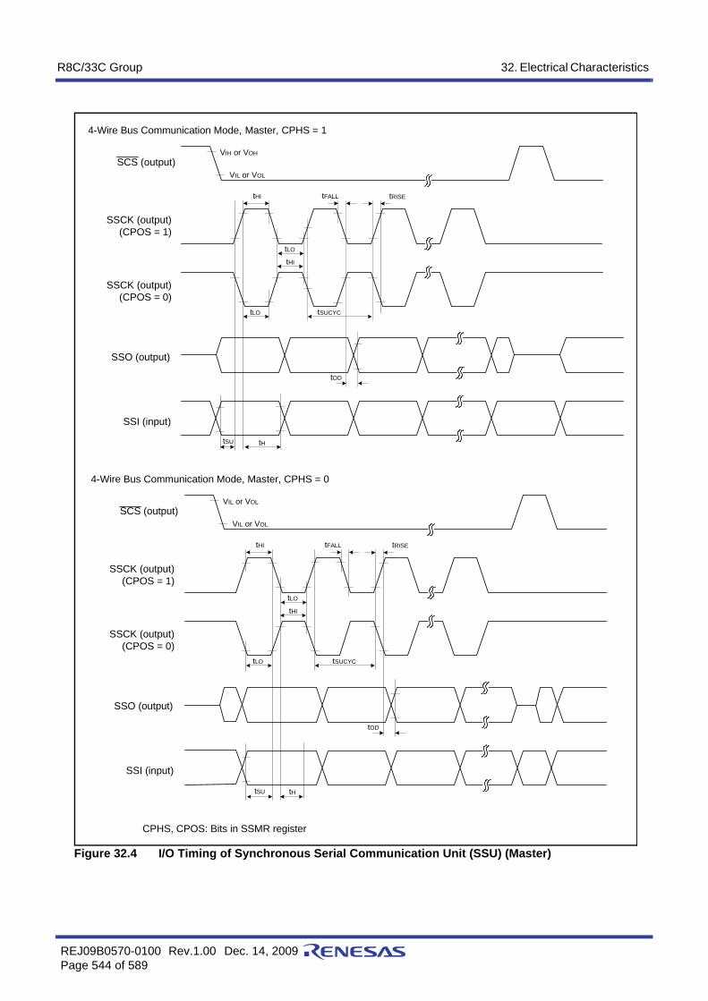
R8C/33C Group 32. Electrical Characteristics
REJ09B0570-0100 Rev.1.00 Dec. 14, 2009Page 544 of 589
Figure 32.4 I/O Timing of Synchronous Serial Communication Unit (SSU) (Master)
VIH or VOH
VIL or VOL
tHI
tLO
tHI
tFALL tRISE
tLO tSUCYC
tOD
tHtSU
SCS (output)
SSCK (output)(CPOS = 1)
SSCK (output)(CPOS = 0)
SSO (output)
SSI (input)
4-Wire Bus Communication Mode, Master, CPHS = 1
VIL or VOL
VIL or VOL
tHI
tLO
tHI
tFALL tRISE
tLO tSUCYC
tOD
tHtSU
SCS (output)
SSCK (output)(CPOS = 1)
SSCK (output)(CPOS = 0)
SSO (output)
SSI (input)
4-Wire Bus Communication Mode, Master, CPHS = 0
CPHS, CPOS: Bits in SSMR register

R8C/33C Group 32. Electrical Characteristics
REJ09B0570-0100 Rev.1.00 Dec. 14, 2009Page 545 of 589
Figure 32.5 I/O Timing of Synchronous Serial Communication Unit (SSU) (Slave)
VIH or VOH
VIL or VOL
SCS (input)
SSCK (input)(CPOS = 1)
SSCK (input)(CPOS = 0)
SSO (input)
SSI (output)
4-Wire Bus Communication Mode, Slave, CPHS = 1
VIH or VOH
VIL or VOL
tHI
tLO
tHI
tFALL tRISE
tLO tSUCYC
tHtSU
SCS (input)
SSCK (input)(CPOS = 1)
SSCK (input)(CPOS = 0)
SSO (input)
SSI (output)
4-Wire Bus Communication Mode, Slave, CPHS = 0
tOD
tLEAD
tSA
tLAG
tOR
tHI
tLO
tHI
tFALL tRISE
tLO tSUCYC
tHtSU
tOD
tLEAD
tSA
tLAG
tOR
CPHS, CPOS: Bits in SSMR register

R8C/33C Group 32. Electrical Characteristics
REJ09B0570-0100 Rev.1.00 Dec. 14, 2009Page 546 of 589
Figure 32.6 I/O Timing of Synchronous Serial Communication Unit (SSU) (Clock Synchronous Communication Mode)
VIH or VOH
tHI
tLO tSUCYC
tOD
tHtSU
SSCK
SSO (output)
SSI (input)
VIL or VOL

R8C/33C Group 32. Electrical Characteristics
REJ09B0570-0100 Rev.1.00 Dec. 14, 2009Page 547 of 589
Notes:1. VCC = 1.8 to 5.5 V, VSS = 0 V and Topr = −20 to 85°C (N version) / −40 to 85°C (D version), unless otherwise specified.2. 1tCYC = 1/f1(s)
Figure 32.7 I/O Timing of I2C bus Interface
Table 32.16 Timing Requirements of I2C bus Interface (1)
Symbol Parameter ConditionStandard
UnitMin. Typ. Max.
tSCL SCL input cycle time 12tCYC + 600 (2) − − nstSCLH SCL input “H” width 3tCYC + 300 (2) − − nstSCLL SCL input “L” width 5tCYC + 500 (2) − − nstsf SCL, SDA input fall time − − 300 nstSP SCL, SDA input spike pulse rejection time − − 1tCYC (2) nstBUF SDA input bus-free time 5tCYC (2) − − nstSTAH Start condition input hold time 3tCYC (2) − − nstSTAS Retransmit start condition input setup time 3tCYC (2) − − nstSTOP Stop condition input setup time 3tCYC (2) − − nstSDAS Data input setup time 1tCYC + 40 (2) − − nstSDAH Data input hold time 10 − − ns
SDA
tSTAH
tSCLL
tBUF
VIH
VIL
tSCLH
SCL
tsrtsf
tSDAHtSCL
tSTAStSP tSTOP
tSDAS
P(2) S(1) Sr(3) P(2)
Notes: 1. Start condition 2. Stop condition 3. Retransmit start condition

R8C/33C Group 32. Electrical Characteristics
REJ09B0570-0100 Rev.1.00 Dec. 14, 2009Page 548 of 589
Note:1. 4.2 V ≤ VCC ≤ 5.5 V and Topr = −20 to 85°C (N version) / −40 to 85°C (D version), f(XIN) = 20 MHz, unless otherwise specified.
Table 32.17 Electrical Characteristics (1) [4.2 V ≤ Vcc ≤ 5.5 V]
Symbol Parameter ConditionStandard
UnitMin. Typ. Max.
VOH Output “H” voltage
Other than XOUT Drive capacity High VCC = 5 V IOH = −20 mA VCC − 2.0 − VCC VDrive capacity Low VCC = 5 V IOH = −5 mA VCC − 2.0 − VCC V
XOUT VCC = 5 V IOH = −200 µA 1.0 − VCC VVOL Output
“L” voltageOther than XOUT Drive capacity High VCC = 5 V IOL = 20 mA − − 2.0 V
Drive capacity Low VCC = 5 V IOL = 5 mA − − 2.0 VXOUT VCC = 5 V IOL = 200 µA − − 0.5 V
VT+-VT- Hysteresis INT0, INT1, INT3, KI0, KI1, KI2, KI3, TRAIO, TRBO, TRCIOA, TRCIOB, TRCIOC, TRCIOD, TRCTRG, TRCCLK, ADTRG, RXD0, RXD1, RXD2, CLK0, CLK1, CLK2, SSI, SCL, SDA, SSO
0.1 1.2 − V
RESET 0.1 1.2 − V
IIH Input “H” current VI = 5 V, VCC = 5.0 V − − 5.0 µAIIL Input “L” current VI = 0 V, VCC = 5.0 V − − −5.0 µARPULLUP Pull-up resistance VI = 0 V, VCC = 5.0 V 25 50 100 kΩRfXIN Feedback
resistanceXIN − 0.3 − MΩ
RfXCIN Feedback resistance
XCIN − 8 − MΩ
VRAM RAM hold voltage During stop mode 1.8 − − V
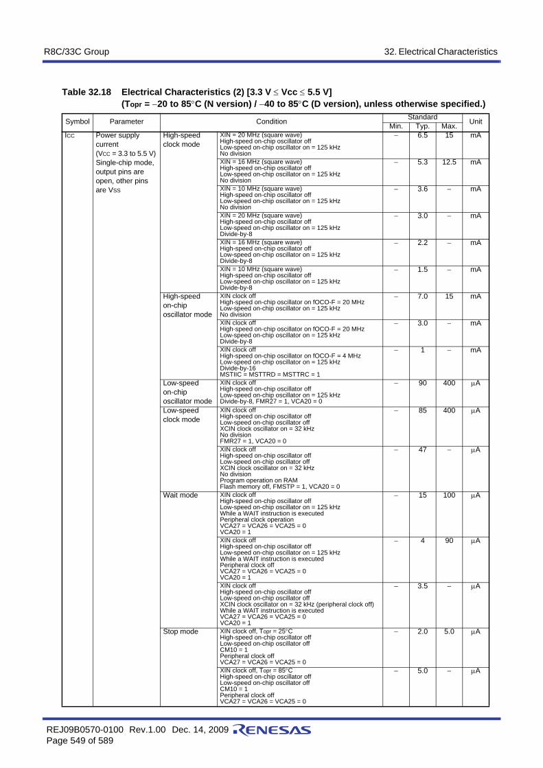
R8C/33C Group 32. Electrical Characteristics
REJ09B0570-0100 Rev.1.00 Dec. 14, 2009Page 549 of 589
Table 32.18 Electrical Characteristics (2) [3.3 V ≤ Vcc ≤ 5.5 V](Topr = −20 to 85°C (N version) / −40 to 85°C (D version), unless otherwise specified.)
Symbol Parameter Condition Standard UnitMin. Typ. Max.ICC Power supply
current (VCC = 3.3 to 5.5 V)Single-chip mode, output pins are open, other pins are VSS
High-speed clock mode
XIN = 20 MHz (square wave)High-speed on-chip oscillator offLow-speed on-chip oscillator on = 125 kHzNo division
− 6.5 15 mA
XIN = 16 MHz (square wave)High-speed on-chip oscillator offLow-speed on-chip oscillator on = 125 kHzNo division
− 5.3 12.5 mA
XIN = 10 MHz (square wave)High-speed on-chip oscillator offLow-speed on-chip oscillator on = 125 kHzNo division
− 3.6 − mA
XIN = 20 MHz (square wave)High-speed on-chip oscillator offLow-speed on-chip oscillator on = 125 kHzDivide-by-8
− 3.0 − mA
XIN = 16 MHz (square wave)High-speed on-chip oscillator offLow-speed on-chip oscillator on = 125 kHzDivide-by-8
− 2.2 − mA
XIN = 10 MHz (square wave)High-speed on-chip oscillator offLow-speed on-chip oscillator on = 125 kHzDivide-by-8
− 1.5 − mA
High-speed on-chip oscillator mode
XIN clock offHigh-speed on-chip oscillator on fOCO-F = 20 MHzLow-speed on-chip oscillator on = 125 kHzNo division
− 7.0 15 mA
XIN clock offHigh-speed on-chip oscillator on fOCO-F = 20 MHzLow-speed on-chip oscillator on = 125 kHzDivide-by-8
− 3.0 − mA
XIN clock offHigh-speed on-chip oscillator on fOCO-F = 4 MHzLow-speed on-chip oscillator on = 125 kHzDivide-by-16MSTIIC = MSTTRD = MSTTRC = 1
− 1 − mA
Low-speed on-chip oscillator mode
XIN clock offHigh-speed on-chip oscillator offLow-speed on-chip oscillator on = 125 kHzDivide-by-8, FMR27 = 1, VCA20 = 0
− 90 400 µA
Low-speed clock mode
XIN clock offHigh-speed on-chip oscillator offLow-speed on-chip oscillator offXCIN clock oscillator on = 32 kHz No divisionFMR27 = 1, VCA20 = 0
− 85 400 µA
XIN clock offHigh-speed on-chip oscillator offLow-speed on-chip oscillator offXCIN clock oscillator on = 32 kHz No divisionProgram operation on RAMFlash memory off, FMSTP = 1, VCA20 = 0
− 47 − µA
Wait mode XIN clock offHigh-speed on-chip oscillator offLow-speed on-chip oscillator on = 125 kHzWhile a WAIT instruction is executedPeripheral clock operationVCA27 = VCA26 = VCA25 = 0VCA20 = 1
− 15 100 µA
XIN clock offHigh-speed on-chip oscillator offLow-speed on-chip oscillator on = 125 kHzWhile a WAIT instruction is executedPeripheral clock offVCA27 = VCA26 = VCA25 = 0VCA20 = 1
− 4 90 µA
XIN clock offHigh-speed on-chip oscillator offLow-speed on-chip oscillator offXCIN clock oscillator on = 32 kHz (peripheral clock off)While a WAIT instruction is executedVCA27 = VCA26 = VCA25 = 0VCA20 = 1
− 3.5 − µA
Stop mode XIN clock off, Topr = 25°CHigh-speed on-chip oscillator offLow-speed on-chip oscillator offCM10 = 1Peripheral clock offVCA27 = VCA26 = VCA25 = 0
− 2.0 5.0 µA
XIN clock off, Topr = 85°CHigh-speed on-chip oscillator offLow-speed on-chip oscillator offCM10 = 1Peripheral clock offVCA27 = VCA26 = VCA25 = 0
− 5.0 − µA
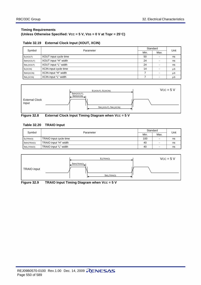
R8C/33C Group 32. Electrical Characteristics
REJ09B0570-0100 Rev.1.00 Dec. 14, 2009Page 550 of 589
Timing Requirements (Unless Otherwise Specified: VCC = 5 V, VSS = 0 V at Topr = 25°C)
Figure 32.8 External Clock Input Timing Diagram when VCC = 5 V
Figure 32.9 TRAIO Input Timing Diagram when VCC = 5 V
Table 32.19 External Clock Input (XOUT, XCIN)
Symbol ParameterStandard
UnitMin. Max.
tc(XOUT) XOUT input cycle time 50 − nstWH(XOUT) XOUT input “H” width 24 − nstWL(XOUT) XOUT input “L” width 24 − nstc(XCIN) XCIN input cycle time 14 − µstWH(XCIN) XCIN input “H” width 7 − µstWL(XCIN) XCIN input “L” width 7 − µs
Table 32.20 TRAIO Input
Symbol ParameterStandard
UnitMin. Max.
tc(TRAIO) TRAIO input cycle time 100 − nstWH(TRAIO) TRAIO input “H” width 40 − nstWL(TRAIO) TRAIO input “L” width 40 − ns
External ClockInput
tWH(XOUT),tWH(XCIN)
tC(XOUT), tC(XCIN)
tWL(XOUT), tWL(XCIN)
VCC = 5 V
TRAIO input
VCC = 5 VtC(TRAIO)
tWL(TRAIO)
tWH(TRAIO)

R8C/33C Group 32. Electrical Characteristics
REJ09B0570-0100 Rev.1.00 Dec. 14, 2009Page 551 of 589
i = 0 to 2
Figure 32.10 Serial Interface Timing Diagram when VCC = 5 V
Notes:1. When selecting the digital filter by the INTi input filter select bit, use an INTi input HIGH width of either (1/digital filter clock
frequency × 3) or the minimum value of standard, whichever is greater.2. When selecting the digital filter by the INTi input filter select bit, use an INTi input LOW width of either (1/digital filter clock
frequency × 3) or the minimum value of standard, whichever is greater.
Figure 32.11 Input Timing Diagram for External Interrupt INTi and Key Input Interrupt KIi when Vcc = 5 V
Table 32.21 Serial Interface
Symbol ParameterStandard
UnitMin. Max.
tc(CK) CLKi input cycle time 200 − nstW(CKH) CLKi input “H” width 100 − nstW(CKL) CLKi input “L” width 100 − nstd(C-Q) TXDi output delay time − 50 nsth(C-Q) TXDi hold time 0 − nstsu(D-C) RXDi input setup time 50 − nsth(C-D) RXDi input hold time 90 − ns
Table 32.22 External Interrupt INTi (i = 0, 1, 3) Input, Key Input Interrupt KIi (i = 0 to 3)
Symbol ParameterStandard
UnitMin. Max.
tW(INH) INTi input “H” width, KIi input “H” width 250 (1) − ns
tW(INL) INTi input “L” width, KIi input “L” width 250 (2) − ns
tW(CKH)
tC(CK)
tW(CKL)
th(C-Q)
th(C-D)tsu(D-C)td(C-Q)
CLKi
TXDi
RXDi
i = 0 to 2
VCC = 5 V
INTi input(i = 0, 1, 3)
tW(INL)
tW(INH)
VCC = 5 V
KIi input(i = 0 to 3)

R8C/33C Group 32. Electrical Characteristics
REJ09B0570-0100 Rev.1.00 Dec. 14, 2009Page 552 of 589
Note:1. 2.7 V ≤ VCC < 4.2 V and Topr = −20 to 85°C (N version) / −40 to 85°C (D version), f(XIN) = 10 MHz, unless otherwise
specified.
Table 32.23 Electrical Characteristics (3) [2.7 V ≤ Vcc < 4.2 V]
Symbol Parameter ConditionStandard
UnitMin. Typ. Max.
VOH Output “H” voltage Other than XOUT Drive capacity High IOH = −5 mA VCC − 0.5 − VCC VDrive capacity Low IOH = −1 mA VCC − 0.5 − VCC V
XOUT IOH = −200 µA 1.0 − VCC VVOL Output “L” voltage Other than XOUT Drive capacity High IOL = 5 mA − − 0.5 V
Drive capacity Low IOL = 1 mA − − 0.5 VXOUT IOL = 200 µA − − 0.5 V
VT+-VT- Hysteresis INT0, INT1, INT3, KI0, KI1, KI2, KI3, TRAIO, TRBO, TRCIOA, TRCIOB, TRCIOC, TRCIOD, TRCTRG, TRCCLK, ADTRG, RXD0, RXD1, RXD2, CLK0, CLK1, CLK2, SSI, SCL, SDA, SSO
VCC = 3.0 V 0.1 0.4 − V
RESET VCC = 3.0 V 0.1 0.5 − V
IIH Input “H” current VI = 3 V, VCC = 3.0 V − − 4.0 µAIIL Input “L” current VI = 0 V, VCC = 3.0 V − − −4.0 µARPULLUP Pull-up resistance VI = 0 V, VCC = 3.0 V 42 84 168 kΩRfXIN Feedback
resistanceXIN − 0.3 − MΩ
RfXCIN Feedback resistance
XCIN − 8 − MΩ
VRAM RAM hold voltage During stop mode 1.8 − − V

R8C/33C Group 32. Electrical Characteristics
REJ09B0570-0100 Rev.1.00 Dec. 14, 2009Page 553 of 589
Table 32.24 Electrical Characteristics (4) [2.7 V ≤ Vcc < 3.3 V](Topr = −20 to 85°C (N version) / −40 to 85°C (D version), unless otherwise specified.)
Symbol Parameter Condition Standard UnitMin. Typ. Max.ICC Power supply current
(VCC = 2.7 to 3.3 V)Single-chip mode, output pins are open, other pins are VSS
High-speed clock mode
XIN = 10 MHz (square wave)High-speed on-chip oscillator offLow-speed on-chip oscillator on = 125 kHzNo division
− 3.5 10 mA
XIN = 10 MHz (square wave)High-speed on-chip oscillator offLow-speed on-chip oscillator on = 125 kHzDivide-by-8
− 1.5 7.5 mA
High-speed on-chip oscillator mode
XIN clock offHigh-speed on-chip oscillator on fOCO-F = 20 MHzLow-speed on-chip oscillator on = 125 kHzNo division
− 7.0 15 mA
XIN clock offHigh-speed on-chip oscillator on fOCO-F = 20 MHzLow-speed on-chip oscillator on = 125 kHzDivide-by-8
− 3.0 − mA
XIN clock offHigh-speed on-chip oscillator on fOCO-F = 10 MHzLow-speed on-chip oscillator on = 125 kHzNo division
− 4.0 − mA
XIN clock offHigh-speed on-chip oscillator on fOCO-F = 10 MHzLow-speed on-chip oscillator on = 125 kHzDivide-by-8
− 1.5 − mA
XIN clock offHigh-speed on-chip oscillator on fOCO-F = 4 MHzLow-speed on-chip oscillator on = 125 kHzDivide-by-16MSTIIC = MSTTRD = MSTTRC = 1
− 1 − mA
Low-speed on-chip oscillator mode
XIN clock offHigh-speed on-chip oscillator offLow-speed on-chip oscillator on = 125 kHzDivide-by-8, FMR27 = 1, VCA20 = 0
− 90 390 µA
Low-speed clock mode
XIN clock offHigh-speed on-chip oscillator offLow-speed on-chip oscillator offXCIN clock oscillator on = 32 kHz No divisionFMR27 = 1, VCA20 = 0
− 80 400 µA
XIN clock offHigh-speed on-chip oscillator offLow-speed on-chip oscillator offXCIN clock oscillator on = 32 kHz No divisionProgram operation on RAMFlash memory off, FMSTP = 1, VCA20 = 0
− 40 − µA
Wait mode XIN clock offHigh-speed on-chip oscillator offLow-speed on-chip oscillator on = 125 kHzWhile a WAIT instruction is executedPeripheral clock operationVCA27 = VCA26 = VCA25 = 0, VCA20 = 1
− 15 90 µA
XIN clock offHigh-speed on-chip oscillator offLow-speed on-chip oscillator on = 125 kHzWhile a WAIT instruction is executedPeripheral clock offVCA27 = VCA26 = VCA25 = 0, VCA20 = 1
− 4 80 µA
XIN clock offHigh-speed on-chip oscillator offLow-speed on-chip oscillator offXCIN clock oscillator on = 32 kHz (peripheral clock off)While a WAIT instruction is executedVCA27 = VCA26 = VCA25 = 0, VCA20 = 1
− 3.5 − µA
Stop mode XIN clock off, Topr = 25°CHigh-speed on-chip oscillator offLow-speed on-chip oscillator offCM10 = 1Peripheral clock offVCA27 = VCA26 = VCA25 = 0
− 2.0 5.0 µA
XIN clock off, Topr = 85°CHigh-speed on-chip oscillator offLow-speed on-chip oscillator offCM10 = 1Peripheral clock offVCA27 = VCA26 = VCA25 = 0
− 5.0 − µA

R8C/33C Group 32. Electrical Characteristics
REJ09B0570-0100 Rev.1.00 Dec. 14, 2009Page 554 of 589
Timing requirements (Unless Otherwise Specified: VCC = 3 V, VSS = 0 V at Topr = 25°C)
Figure 32.12 External Clock Input Timing Diagram when VCC = 3 V
Figure 32.13 TRAIO Input Timing Diagram when VCC = 3 V
Table 32.25 External Clock Input (XOUT, XCIN)
Symbol ParameterStandard
UnitMin. Max.
tc(XOUT) XOUT input cycle time 50 − nstWH(XOUT) XOUT input “H” width 24 − nstWL(XOUT) XOUT input “L” width 24 − nstc(XCIN) XCIN input cycle time 14 − µstWH(XCIN) XCIN input “H” width 7 − µstWL(XCIN) XCIN input “L” width 7 − µs
Table 32.26 TRAIO Input
Symbol ParameterStandard
UnitMin. Max.
tc(TRAIO) TRAIO input cycle time 300 − nstWH(TRAIO) TRAIO input “H” width 120 − nstWL(TRAIO) TRAIO input “L” width 120 − ns
External Clock Input
tWH(XOUT),tWH(XCIN)
tC(XOUT), tC(XCIN)
tWL(XOUT), tWL(XCIN)
VCC = 3 V
TRAIO input
VCC = 3 VtC(TRAIO)
tWL(TRAIO)
tWH(TRAIO)

R8C/33C Group 32. Electrical Characteristics
REJ09B0570-0100 Rev.1.00 Dec. 14, 2009Page 555 of 589
i = 0 to 2
Figure 32.14 Serial Interface Timing Diagram when VCC = 3 V
Notes:1. When selecting the digital filter by the INTi input filter select bit, use an INTi input HIGH width of either (1/digital filter clock
frequency × 3) or the minimum value of standard, whichever is greater.2. When selecting the digital filter by the INTi input filter select bit, use an INTi input LOW width of either (1/digital filter clock
frequency × 3) or the minimum value of standard, whichever is greater.
Figure 32.15 Input Timing Diagram for External Interrupt INTi and Key Input Interrupt KIi when Vcc = 3 V
Table 32.27 Serial Interface
Symbol ParameterStandard
UnitMin. Max.
tc(CK) CLKi input cycle time 300 − nstW(CKH) CLKi input “H” width 150 − nstW(CKL) CLKi Input “L” width 150 − nstd(C-Q) TXDi output delay time − 80 nsth(C-Q) TXDi hold time 0 − nstsu(D-C) RXDi input setup time 70 − nsth(C-D) RXDi input hold time 90 − ns
Table 32.28 External Interrupt INTi (i = 0, 1, 3) Input, Key Input Interrupt KIi (i = 0 to 3)
Symbol ParameterStandard
UnitMin. Max.
tW(INH) INTi input “H” width, KIi input “H” width 380 (1) − ns
tW(INL) INTi input “L” width, KIi input “L” width 380 (2) − ns
tW(CKH)
tC(CK)
tW(CKL)
th(C-Q)
th(C-D)tsu(D-C)td(C-Q)
CLKi
TXDi
RXDi
VCC = 3 V
i = 0 to 2
tW(INL)
tW(INH)
VCC = 3 VINTi input(i = 0, 1, 3)
KIi input(i = 0 to 3)

R8C/33C Group 32. Electrical Characteristics
REJ09B0570-0100 Rev.1.00 Dec. 14, 2009Page 556 of 589
Note:1. 1.8 V ≤ VCC < 2.7 V and Topr = −20 to 85°C (N version) / −40 to 85°C (D version), f(XIN) = 5 MHz, unless otherwise specified.
Table 32.29 Electrical Characteristics (5) [1.8 V ≤ Vcc < 2.7 V]
Symbol Parameter ConditionStandard
UnitMin. Typ. Max.
VOH Output “H” voltage Other than XOUT Drive capacity High IOH = −2 mA VCC − 0.5 − VCC VDrive capacity Low IOH = −1 mA VCC − 0.5 − VCC V
XOUT IOH = −200 µA 1.0 − VCC VVOL Output “L” voltage Other than XOUT Drive capacity High IOL = 2 mA − − 0.5 V
Drive capacity Low IOL = 1 mA − − 0.5 VXOUT IOL = 200 µA − − 0.5 V
VT+-VT- Hysteresis INT0, INT1, INT3, KI0, KI1, KI2, KI3, TRAIO, TRBO, TRCIOA, TRCIOB, TRCIOC, TRCIOD, TRCTRG, TRCCLK, ADTRG, RXD0, RXD1, RXD2, CLK0, CLK1, CLK2, SSI, SCL, SDA, SSO
0.05 0.20 − V
RESET 0.05 0.2 − V
IIH Input “H” current VI = 2.2 V, VCC = 2.2 V − − 4.0 µAIIL Input “L” current VI = 0 V, VCC = 2.2 V − − −4.0 µARPULLUP Pull-up resistance VI = 0 V, VCC = 2.2 V 70 140 300 kΩRfXIN Feedback
resistanceXIN − 0.3 − MΩ
RfXCIN Feedback resistance
XCIN − 8 − MΩ
VRAM RAM hold voltage During stop mode 1.8 − − V

R8C/33C Group 32. Electrical Characteristics
REJ09B0570-0100 Rev.1.00 Dec. 14, 2009Page 557 of 589
Table 32.30 Electrical Characteristics (6) [1.8 V ≤ Vcc < 2.7 V](Topr = −20 to 85°C (N version) / −40 to 85°C (D version), unless otherwise specified.)
Symbol Parameter ConditionStandard
UnitMin. Typ. Max.
ICC Power supply current (VCC = 1.8 to 2.7 V)Single-chip mode, output pins are open, other pins are VSS
High-speed clock mode
XIN = 5 MHz (square wave)High-speed on-chip oscillator offLow-speed on-chip oscillator on = 125 kHzNo division
− 2.2 − mA
XIN = 5 MHz (square wave)High-speed on-chip oscillator offLow-speed on-chip oscillator on = 125 kHzDivide-by-8
− 0.8 − mA
High-speed on-chip oscillator mode
XIN clock offHigh-speed on-chip oscillator on fOCO-F = 5 MHzLow-speed on-chip oscillator on = 125 kHzNo division
− 2.5 10 mA
XIN clock offHigh-speed on-chip oscillator on fOCO-F = 5 MHzLow-speed on-chip oscillator on = 125 kHzDivide-by-8
− 1.7 − mA
XIN clock offHigh-speed on-chip oscillator on fOCO-F = 4 MHzLow-speed on-chip oscillator on = 125 kHzDivide-by-16MSTIIC = MSTTRD = MSTTRC = 1
− 1 − mA
Low-speed on-chip oscillator mode
XIN clock offHigh-speed on-chip oscillator offLow-speed on-chip oscillator on = 125 kHzDivide-by-8, FMR27 = 1, VCA20 = 0
− 90 300 µA
Low-speed clock mode
XIN clock offHigh-speed on-chip oscillator offLow-speed on-chip oscillator offXCIN clock oscillator on = 32 kHz No divisionFMR27 = 1, VCA20 = 0
− 80 350 µA
XIN clock offHigh-speed on-chip oscillator offLow-speed on-chip oscillator offXCIN clock oscillator on = 32 kHz No divisionProgram operation on RAMFlash memory off, FMSTP = 1, VCA20 = 0
− 40 − µA
Wait mode XIN clock offHigh-speed on-chip oscillator offLow-speed on-chip oscillator on = 125 kHzWhile a WAIT instruction is executedPeripheral clock operationVCA27 = VCA26 = VCA25 = 0VCA20 = 1
− 15 90 µA
XIN clock offHigh-speed on-chip oscillator offLow-speed on-chip oscillator on = 125 kHzWhile a WAIT instruction is executedPeripheral clock offVCA27 = VCA26 = VCA25 = 0VCA20 = 1
− 4 80 µA
XIN clock offHigh-speed on-chip oscillator offLow-speed on-chip oscillator offXCIN clock oscillator on = 32 kHz (peripheral clock off)While a WAIT instruction is executedVCA27 = VCA26 = VCA25 = 0VCA20 = 1
− 3.5 − µA
Stop mode XIN clock off, Topr = 25°CHigh-speed on-chip oscillator offLow-speed on-chip oscillator offCM10 = 1Peripheral clock offVCA27 = VCA26 = VCA25 = 0
− 2.0 5 µA
XIN clock off, Topr = 85°CHigh-speed on-chip oscillator offLow-speed on-chip oscillator offCM10 = 1Peripheral clock offVCA27 = VCA26 = VCA25 = 0
− 5.0 − µA

R8C/33C Group 32. Electrical Characteristics
REJ09B0570-0100 Rev.1.00 Dec. 14, 2009Page 558 of 589
Timing requirements (Unless Otherwise Specified: VCC = 2.2 V, VSS = 0 V at Topr = 25°C)
Figure 32.16 External Clock Input Timing Diagram when VCC = 2.2 V
Figure 32.17 TRAIO Input Timing Diagram when VCC = 2.2 V
Table 32.31 External Clock Input (XOUT, XCIN)
Symbol ParameterStandard
UnitMin. Max.
tc(XOUT) XOUT input cycle time 200 − nstWH(XOUT) XOUT input “H” width 90 − nstWL(XOUT) XOUT input “L” width 90 − nstc(XCIN) XCIN input cycle time 14 − µstWH(XCIN) XCIN input “H” width 7 − µstWL(XCIN) XCIN input “L” width 7 − µs
Table 32.32 TRAIO Input
Symbol ParameterStandard
UnitMin. Max.
tc(TRAIO) TRAIO input cycle time 500 − nstWH(TRAIO) TRAIO input “H” width 200 − nstWL(TRAIO) TRAIO input “L” width 200 − ns
External Clock Input
tWH(XOUT),tWH(XCIN)
tC(XOUT), tC(XCIN)
tWL(XOUT), tWL(XCIN)
VCC = 2.2 V
TRAIO input
tC(TRAIO)
tWL(TRAIO)
tWH(TRAIO)
VCC = 2.2 V

R8C/33C Group 32. Electrical Characteristics
REJ09B0570-0100 Rev.1.00 Dec. 14, 2009Page 559 of 589
i = 0 to 2
Figure 32.18 Serial Interface Timing Diagram when VCC = 2.2 V
Notes:1. When selecting the digital filter by the INTi input filter select bit, use an INTi input HIGH width of either (1/digital filter clock
frequency × 3) or the minimum value of standard, whichever is greater.2. When selecting the digital filter by the INTi input filter select bit, use an INTi input LOW width of either (1/digital filter clock
frequency × 3) or the minimum value of standard, whichever is greater.
Figure 32.19 Input Timing Diagram for External Interrupt INTi and Key Input Interrupt KIi when Vcc = 2.2 V
Table 32.33 Serial Interface
Symbol ParameterStandard
UnitMin. Max.
tc(CK) CLKi input cycle time 800 − nstW(CKH) CLKi input “H” width 400 − nstW(CKL) CLKi input “L” width 400 − nstd(C-Q) TXDi output delay time − 200 nsth(C-Q) TXDi hold time 0 − nstsu(D-C) RXDi input setup time 150 − nsth(C-D) RXDi input hold time 90 − ns
Table 32.34 External Interrupt INTi (i = 0, 1, 3) Input, Key Input Interrupt KIi (i = 0 to 3)
Symbol ParameterStandard
UnitMin. Max.
tW(INH) INTi input “H” width, KIi input “H” width 1000 (1) − ns
tW(INL) INTi input “L” width, KIi input “L” width 1000 (2) − ns
tW(CKH)
tC(CK)
tW(CKL)
th(C-Q)
th(C-D)tsu(D-C)td(C-Q)
CLKi
TXDi
RXDi
VCC = 2.2 V
i = 0 to 2
tW(INL)
tW(INH)
VCC = 2.2 VINTi input(i = 0, 1, 3)
KIi input(i = 0 to 3)

R8C/33C Group 33. Usage Notes
REJ09B0570-0100 Rev.1.00 Dec. 14, 2009Page 560 of 589
33. Usage Notes
33.1 Notes on Clock Generation Circuit
33.1.1 Stop ModeTo enter stop mode, set the FMR01 bit in the FMR0 register to 0 (CPU rewrite mode disabled) and then theCM10 bit in the CM1 register to 1 (stop mode). An instruction queue pre-reads 4 bytes from the instructionwhich sets the CM10 bit to 1 (stop mode) and the program stops.Insert at least four NOP instructions following the JMP.B instruction after the instruction which sets the CM10bit to 1.
• Program example to enter stop modeBCLR 1,FMR0 ; CPU rewrite mode disabledBCLR 7,FMR2 ; Low-current-consumption read mode disabledBSET 0,PRCR ; Writing to CM1 register enabledFSET I ; Interrupt enabledBSET 0,CM1 ; Stop modeJMP.B LABEL_001
LABEL_001:NOPNOPNOPNOP
33.1.2 Wait ModeTo enter wait mode by setting the CM30 bit to 1, set the FMR01 bit in the FMR0 register to 0 (CPU rewritemode disabled) before setting the CM30 bit to 1.To enter wait mode with the WAIT instruction, set the FMR01 bit in the FMR0 register to 0 (CPU rewrite modedisabled) and then execute the WAIT instruction. An instruction queue pre-reads 4 bytes from the instruction toset the CM30 bit to 1 (MCU enters wait mode) or the WAIT instruction, and then the program stops. Insert atleast four NOP instructions after the instruction to set the CM30 bit to 1 (MCU enters wait mode) or the WAITinstruction.
• Program example to execute the WAIT instructionBCLR 1,FMR0 ; CPU rewrite mode disabledBCLR 7,FMR2 ; Low-current-consumption read mode disabledFSET I ; Interrupt enabledWAIT ; Wait modeNOPNOPNOPNOP
• Program example to execute the instruction to set the CM30 bit to 1BCLR 1, FMR0 ; CPU rewrite mode disabledBCLR 7,FMR2 ; Low-current-consumption read mode disabledBSET 0, PRCR ; Writing to CM3 register enabledFCLR I ; Interrupt disabledBSET 0, CM3 ; Wait modeNOPNOPNOPNOPBCLR 0, PRCR ; Writing to CM3 register disabledFSET I ; Interrupt enabled

R8C/33C Group 33. Usage Notes
REJ09B0570-0100 Rev.1.00 Dec. 14, 2009Page 561 of 589
33.1.3 Oscillation Stop Detection FunctionSince the oscillation stop detection function cannot be used if the XIN clock frequency is below 2 MHz, set bitsOCD1 to OCD0 to 00b.
33.1.4 Oscillation Circuit ConstantsConsult the oscillator manufacturer to determine the optimal oscillation circuit constants for the user system.To use the MCU with supply voltage below VCC = 2.7 V, it is recommended to set the CM11 bit in the CM1register to 1 (on-chip feedback resistor disabled) and connect the feedback resistor to the chip externally.

R8C/33C Group 33. Usage Notes
REJ09B0570-0100 Rev.1.00 Dec. 14, 2009Page 562 of 589
33.2 Notes on Interrupts
33.2.1 Reading Address 00000hDo not read address 00000h by a program. When a maskable interrupt request is acknowledged, the CPU readsinterrupt information (interrupt number and interrupt request level) from 00000h in the interrupt sequence. Atthis time, the IR bit for the acknowledged interrupt is set to 0.If address 00000h is read by a program, the IR bit for the interrupt which has the highest priority among theenabled interrupts is set to 0. This may cause the interrupt to be canceled, or an unexpected interrupt to begenerated.
33.2.2 SP SettingSet a value in the SP before an interrupt is acknowledged. The SP is set to 0000h after a reset. If an interrupt isacknowledged before setting a value in the SP, the program may run out of control.
33.2.3 External Interrupt and Key Input InterruptEither the “L” level width or “H” level width shown in the Electrical Characteristics is required for the signalinput to pins INT0, INT1, INT3 and pins KI0 to KI3, regardless of the CPU clock.For details, refer to Table 32.22 (VCC = 5V), Table 32.28 (VCC = 3V), Table 32.34 (VCC = 2.2V) ExternalInterrupt INTi (i = 0, 1, 3) Input, Key Input Interrupt KIi (i = 0 to 3).

R8C/33C Group 33. Usage Notes
REJ09B0570-0100 Rev.1.00 Dec. 14, 2009Page 563 of 589
33.2.4 Changing Interrupt SourcesThe IR bit in the interrupt control register may be set to 1 (interrupt requested) when the interrupt sourcechanges. To use an interrupt, set the IR bit to 0 (no interrupt requested) after changing interrupt sources.Changing interrupt sources as referred to here includes all factors that change the source, polarity, or timing ofthe interrupt assigned to a software interrupt number. Therefore, if a mode change of a peripheral functioninvolves the source, polarity, or timing of an interrupt, set the IR bit to 0 (no interrupt requested) after makingthese changes. Refer to the descriptions of the individual peripheral functions for related interrupts. Figure 33.1 shows a Procedure Example for Changing Interrupt Sources.
Figure 33.1 Procedure Example for Changing Interrupt Sources
Notes:1. The above settings must be executed individually. Do not execute two or more settings
simultaneously (using one instruction).2. To prevent interrupt requests from being generated disable the peripheral function
before changing the interrupt source. In this case, use the I flag if all maskableinterrupts can be disabled.If all maskable interrupts cannot be disabled, use bits ILVL0 to ILVL2 for the interruptwhose source is to be changed.
3. To change the interrupt source to the input with the digital filter used, wait for three ormore cycles of the sampling clock of the digital filter before setting the IR bit to 0 (nointerrupt request). Refer to 11.8.5 Rewriting Interrupt Control Register for theinstructions to use and related notes.
Interrupt source change
Disable interrupts (2, 3)
Set the IR bit to 0 (no interrupt request)using the MOV instruction (3)
Change interrupt sources(including mode of peripheral function)
Enable interrupts (2, 3)
Change completed
IR bit: The interrupt control register bit for the interrupt whose source is to be changed

R8C/33C Group 33. Usage Notes
REJ09B0570-0100 Rev.1.00 Dec. 14, 2009Page 564 of 589
33.2.5 Rewriting Interrupt Control Register(a) The contents of the interrupt control register can be rewritten only while no interrupt requests
corresponding to that register are generated. If an interrupt request may be generated, disable the interruptbefore rewriting the contents of the interrupt control register.
(b) When rewriting the contents of the interrupt control register after disabling the interrupt, be careful tochoose appropriate instructions.Changing any bit other than the IR bitIf an interrupt request corresponding to the register is generated while executing the instruction, the IR bitmay not be set to 1 (interrupt requested), and the interrupt may be ignored. If this causes a problem, use oneof the following instructions to rewrite the contents of the register: AND, OR, BCLR, and BSET.
Changing the IR bitDepending on the instruction used, the IR bit may not be set to 0 (no interrupt requested). Use the MOV instruction to set the IR bit to 0.
(c) When using the I flag to disable an interrupt, set the I flag as shown in the sample programs below. Refer to(b) regarding rewriting the contents of interrupt control registers using the sample programs.
Examples 1 to 3 shows how to prevent the I flag from being set to 1 (interrupts enabled) before the contents ofthe interrupt control register are rewritten for the effects of the internal bus and the instruction queue buffer.
Example 1: Use the NOP instructions to pause program until the interrupt control register is rewrittenINT_SWITCH1:
FCLR I ; Disable interruptsAND.B #00H,0056H ; Set the TRAIC register to 00hNOP ;NOPFSET I ; Enable interrupts
Example 2: Use a dummy read to delay the FSET instructionINT_SWITCH2:
FCLR I ; Disable interruptsAND.B #00H,0056H ; Set the TRAIC register to 00hMOV.W MEM,R0 ; Dummy readFSET I ; Enable interrupts
Example 3: Use the POPC instruction to change the I flagINT_SWITCH3:
PUSHC FLGFCLR I ; Disable interruptsAND.B #00H,0056H ; Set the TRAIC register to 00hPOPC FLG ; Enable interrupts

R8C/33C Group 33. Usage Notes
REJ09B0570-0100 Rev.1.00 Dec. 14, 2009Page 565 of 589
33.3 Notes on ID Code Areas
33.3.1 Setting Example of ID Code AreasThe ID code areas are allocated in the flash memory, not in the SFRs. Set appropriate values as ROM data by aprogram. The following shows a setting example.
• To set 55h in all of the ID code areas.org 00FFDCH.lword dummy | (55000000h) ; UND.lword dummy | (55000000h) ; INTO.lword dummy ; BREAK.lword dummy | (55000000h) ; ADDRESS MATCH.lword dummy | (55000000h) ; SET SINGLE STEP.lword dummy | (55000000h) ; WDT.lword dummy | (55000000h) ; ADDRESS BREAK.lword dummy | (55000000h) ; RESERVE
(Programming formats vary depending on the compiler. Check the compiler manual.)
33.4 Notes on Option Function Select Area
33.4.1 Setting Example of Option Function Select AreaThe option function select area is allocated in the flash memory, not in the SFRs. Set appropriate values asROM data by a program. The following shows a setting example.
• To set FFh in the OFS register.org 00FFFCH.lword reset | (0FF000000h) ; RESET
(Programming formats vary depending on the compiler. Check the compiler manual.)
• To set FFh in the OFS2 register.org 00FFDBH.byte 0FFh
(Programming formats vary depending on the compiler. Check the compiler manual.)

R8C/33C Group 33. Usage Notes
REJ09B0570-0100 Rev.1.00 Dec. 14, 2009Page 566 of 589
33.5 Notes on DTC
33.5.1 DTC activation source• Do not generate any DTC activation sources before entering wait mode or during wait mode. • Do not generate any DTC activation sources before entering stop mode or during stop mode.
33.5.2 DTCENi (i = 0 to 3, 5, 6) Registers• Modify bits DTCENi0 to DTCENi7 only while an interrupt request corresponding to the bit is not generated.• When the interrupt source flag in the status register for the peripheral function is 1, do not modify the
corresponding activation source bit among bits DTCENi0 to DTCENi7.• Do not access the DTCENi registers using DTC transfers.
33.5.3 Peripheral Modules• Do not set the status register bit for the peripheral function to 0 using a DTC transfer.• When the DTC activation source is SSU/I2C bus receive data full, read the SSRDR register/the ICDRR
register using a DTC transfer.The RDRF bit in the SSSR register/the ICSR register is set to 0 (no data in SSRDR/ICDRR register) byreading the SSRDR register/the ICDRR register.However, the RDRF bit is not set to 0 by reading the SSRDR register/the ICDRR register when the DTC datatransfer setting is either of the following:- Transfer causing the DTCCTj (j = 0 to 23) register value to change from 1 to 0 in normal mode- Transfer causing the DTCCRj register value to change from 1 to 0 while the RPTINT bit in the DTCCRj
register is 1 (interrupt generation enabled) in repeat mode• When the DTC activation source is SSU/I2C bus transmit data empty, write to the SSTDR register/the ICDRT
register using a DTC transfer. The TDRE bit in the SSSR register/the ICSR register is set to 0 (data is nottransferred from registers SSTDR/ICDRT to SSTRSR/ICDRS) by writing to the SSTDR register/the ICDRTregister.
33.5.4 Interrupt RequestNo interrupt is generated for the CPU during DTC operation in any of the following cases:- When the DTC activation source is SSU/I2C transmit data empty or flash ready status- When performing the data transfer causing the DTCCTj (j = 0 to 23) register value to change to 0 in normal
mode- When performing the data transfer causing the DTCCRj register value to change to 0 while the RPTINT bit in
the DTCCRj register is 1 (interrupt generation enabled) in repeat mode

R8C/33C Group 33. Usage Notes
REJ09B0570-0100 Rev.1.00 Dec. 14, 2009Page 567 of 589
33.6 Notes on Timer RA• Timer RA stops counting after a reset. Set the values in the timer RA and timer RA prescalers before the count
starts.• Even if the prescaler and timer RA are read out in 16-bit units, these registers are read 1 byte at a time by the
MCU. Consequently, the timer value may be updated during the period when these two registers are being read.• In pulse width measurement mode and pulse period measurement mode, bits TEDGF and TUNDF in the TRACR
register can be set to 0 by writing 0 to these bits by a program. However, these bits remain unchanged if 1 iswritten. When using the READ-MODIFY-WRITE instruction for the TRACR register, the TEDGF or TUNDFbit may be set to 0 although these bits are set to 1 while the instruction is being executed. In this case, write 1 tothe TEDGF or TUNDF bit which is not supposed to be set to 0 with the MOV instruction.
• When changing to pulse period measurement mode from another mode, the contents of bits TEDGF and TUNDFare undefined. Write 0 to bits TEDGF and TUNDF before the count starts.
• The TEDGF bit may be set to 1 by the first timer RA prescaler underflow generated after the count starts.• When using the pulse period measurement mode, leave two or more periods of the timer RA prescaler
immediately after the count starts, then set the TEDGF bit to 0.• The TCSTF bit retains 0 (count stops) for 0 to 1 cycle of the count source after setting the TSTART bit to 1 (count
starts) while the count is stopped.During this time, do not access registers associated with timer RA (1) other than the TCSTF bit. Timer RA startscounting at the first valid edge of the count source after the TCSTF bit is set to 1 (during count).The TCSTF bit remains 1 for 0 to 1 cycle of the count source after setting the TSTART bit to 0 (count stops)while the count is in progress. Timer RA counting is stopped when the TCSTF bit is set to 0.During this time, do not access registers associated with timer RA (1) other than the TCSTF bit.
Note:1. Registers associated with timer RA: TRACR, TRAIOC, TRAMR, TRAPRE, and TRA.
• When the TRAPRE register is continuously written during count operation (TCSTF bit is set to 1), allow three ormore cycles of the count source clock for each write interval.
• When the TRA register is continuously written during count operation (TCSTF bit is set to 1), allow three ormore cycles of the prescaler underflow for each write interval.

R8C/33C Group 33. Usage Notes
REJ09B0570-0100 Rev.1.00 Dec. 14, 2009Page 568 of 589
33.7 Notes on Timer RB• Timer RB stops counting after a reset. Set the values in the timer RB and timer RB prescalers before the count
starts.• Even if the prescaler and timer RB is read out in 16-bit units, these registers are read 1 byte at a time by the MCU.
Consequently, the timer value may be updated during the period when these two registers are being read.• In programmable one-shot generation mode and programmable wait one-shot generation mode, when setting the
TSTART bit in the TRBCR register to 0 (stops counting) or setting the TOSSP bit in the TRBOCR register to 1(stops one-shot), the timer reloads the value of reload register and stops. Therefore, in programmable one-shotgeneration mode and programmable wait one-shot generation mode, read the timer count value before the timerstops.
• The TCSTF bit remains 0 (count stops) for 1 to 2 cycles of the count source after setting the TSTART bit to 1(count starts) while the count is stopped.During this time, do not access registers associated with timer RB (1) other than the TCSTF bit. Timer RB startscounting at the first valid edge of the count source after the TCSTF bit is set to 1 (during count).The TCSTF bit remains 1 for 1 to 2 cycles of the count source after setting the TSTART bit to 0 (count stops)while the count is in progress. Timer RB counting is stopped when the TCSTF bit is set to 0.During this time, do not access registers associated with timer RB (1) other than the TCSTF bit.
Note:1. Registers associated with timer RB: TRBCR, TRBOCR, TRBIOC, TRBMR, TRBPRE, TRBSC, and
TRBPR.
• If the TSTOP bit in the TRBCR register is set to 1 during timer operation, timer RB stops immediately.• If 1 is written to the TOSST or TOSSP bit in the TRBOCR register, the value of the TOSSTF bit changes after
one or two cycles of the count source have elapsed. If the TOSSP bit is written to 1 during the period betweenwhen the TOSST bit is written to 1 and when the TOSSTF bit is set to 1, the TOSSTF bit may be set to either 0 or1 depending on the content state. Likewise, if the TOSST bit is written to 1 during the period between when theTOSSP bit is written to 1 and when the TOSSTF bit is set to 0, the TOSSTF bit may be set to either 0 or 1.
• To use the underflow signal of timer RA as the count source for timer RB, set timer RA in timer mode, pulseoutput mode, or event count mode.
33.7.1 Timer ModeTo write to registers TRBPRE and TRBPR during count operation (TCSTF bit in the TRBCR register is set to1), note the following points:• When the TRBPRE register is written continuously, allow three or more cycles of the count source for each
write interval. • When the TRBPR register is written continuously, allow three or more cycles of the prescaler underflow for
each write interval.
33.7.2 Programmable Waveform Generation ModeTo write to registers TRBPRE and TRBPR during count operation (TCSTF bit in the TRBCR register is set to1), note the following points:• When the TRBPRE register is written continuously, allow three or more cycles of the count source for each
write interval. • When the TRBPR register is written continuously, allow three or more cycles of the prescaler underflow for
each write interval.

R8C/33C Group 33. Usage Notes
REJ09B0570-0100 Rev.1.00 Dec. 14, 2009Page 569 of 589
33.7.3 Programmable One-shot Generation ModeTo write to registers TRBPRE and TRBPR during count operation (TCSTF bit in the TRBCR register is set to1), note the following points:• When the TRBPRE register is written continuously during count operation (TCSTF bit is set to 1), allow three
or more cycles of the count source for each write interval. • When the TRBPR register is written continuously during count operation (TCSTF bit is set to 1), allow three
or more cycles of the prescaler underflow for each write interval.
33.7.4 Programmable Wait One-shot Generation ModeTo write to registers TRBPRE and TRBPR during count operation (TCSTF bit in the TRBCR register is set to1), note the following points:• When the TRBPRE register is written continuously, allow three or more cycles of the count source for each
write interval. • When the TRBPR register is written continuously, allow three or more cycles of the prescaler underflow for
each write interval.

R8C/33C Group 33. Usage Notes
REJ09B0570-0100 Rev.1.00 Dec. 14, 2009Page 570 of 589
33.8 Notes on Timer RC
33.8.1 TRC Register• The following note applies when the CCLR bit in the TRCCR1 register is set to 1 (clear TRC register at
compare match with TRCGRA register). When using a program to write a value to the TRC register while the TSTART bit in the TRCMR register isset to 1 (count starts), ensure that the write does not overlap with the timing with which the TRC register is setto 0000h.If the timing of the write to the TRC register and the setting of the TRC register to 0000h coincide, the writevalue will not be written to the TRC register and the TRC register will be set to 0000h.
• Reading from the TRC register immediately after writing to it can result in the value previous to the writebeing read out. To prevent this, execute the JMP.B instruction between the read and the write instructions.
Program Example MOV.W #XXXXh, TRC ;WriteJMP.B L1 ;JMP.B instruction
L1: MOV.W TRC,DATA ;Read
33.8.2 TRCSR RegisterReading from the TRCSR register immediately after writing to it can result in the value previous to the writebeing read out. To prevent this, execute the JMP.B instruction between the read and the write instructions.
Program Example MOV.B #XXh, TRCSR ;WriteJMP.B L1 ;JMP.B instruction
L1: MOV.B TRCSR,DATA ;Read
33.8.3 TRCCR1 RegisterTo set bits TCK2 to TCK0 in the TRCCR1 register to 111b (fOCO-F), set fOCO-F to the clock frequencyhigher than the CPU clock frequency.
33.8.4 Count Source Switching• Stop the count before switching the count source.Switching procedure(1) Set the TSTART bit in the TRCMR register to 0 (count stops).(2) Change the settings of bits TCK2 to TCK0 in the TRCCR1 register.
• After switching the count source from fOCO40M to another clock, allow a minimum of two cycles of f1 toelapse after changing the clock setting before stopping fOCO40M.
Switching procedure(1) Set the TSTART bit in the TRCMR register to 0 (count stops).(2) Change the settings of bits TCK2 to TCK0 in the TRCCR1 register.(3) Wait for a minimum of two cycles of f1.(4) Set the FRA00 bit in the FRA0 register to 0 (high-speed on-chip oscillator off).

R8C/33C Group 33. Usage Notes
REJ09B0570-0100 Rev.1.00 Dec. 14, 2009Page 571 of 589
• After switching the count source from fOCO-F to fOCO40M, allow a minimum of two cycles of fOCO-F toelapse after changing the clock setting before stopping fOCO-F.
Switching procedure(1) Set the TSTART bit in the TRCMR register to 0 (count stops).(2) Change the settings of bits TCK2 to TCK0 in the TRCCR1 register.(3) Wait for a minimum of two cycles of fOCO-F.(4) Set the FRA00 bit in the FRA0 register to 0 (high-speed on-chip oscillator off).
• After switching the count source from fOCO-F to a clock other than fOCO40M, allow a minimum of onecycle of fOCO-F + fOCO40M to elapse after changing the clock setting before stopping fOCO-F.
Switching procedure(1) Set the TSTART bit in the TRCMR register to 0 (count stops).(2) Change the settings of bits TCK2 to TCK0 in the TRCCR1 register.(3) Wait for a minimum of one cycle of fOCO-F + fOCO40M.(4) Set the FRA00 bit in the FRA0 register to 0 (high-speed on-chip oscillator off).
33.8.5 Input Capture Function• Set the pulse width of the input capture signal as follows:
[When the digital filter is not used]Three or more cycles of the timer RC operation clock (refer to Table 19.1 Timer RC Operation Clock)[When the digital filter is used]Five cycles of the digital filter sampling clock + three cycles of the timer RC operating clock, minimum (referto Figure 19.5 Digital Filter Block Diagram)
• The value of the TRC register is transferred to the TRCGRj register one or two cycles of the timer RCoperation clock after the input capture signal is input to the TRCIOj (j = A, B, C, or D) pin (when the digitalfilter function is not used).
33.8.6 TRCMR Register in PWM2 ModeWhen the CSEL bit in the TRCCR2 register is set to 1 (count stops at compare match with the TRCGRAregister), do not set the TRCMR register at compare match timing of registers TRC and TRCGRA.
33.8.7 Count Source fOCO40MThe count source fOCO40M can be used with supply voltage VCC = 2.7 to 5.5 V. For supply voltage other thanthat, do not set bits TCK2 to TCK0 in the TRCCR1 register to 110b (select fOCO40M as the count source).
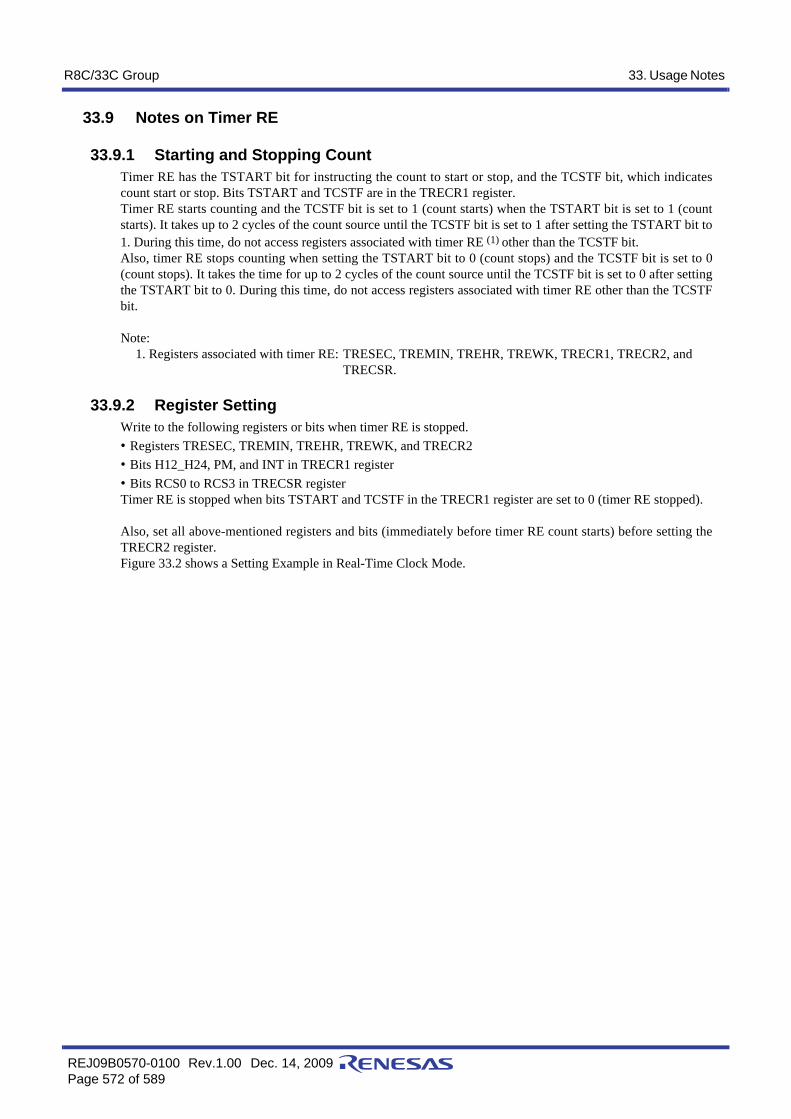
R8C/33C Group 33. Usage Notes
REJ09B0570-0100 Rev.1.00 Dec. 14, 2009Page 572 of 589
33.9 Notes on Timer RE
33.9.1 Starting and Stopping CountTimer RE has the TSTART bit for instructing the count to start or stop, and the TCSTF bit, which indicatescount start or stop. Bits TSTART and TCSTF are in the TRECR1 register.Timer RE starts counting and the TCSTF bit is set to 1 (count starts) when the TSTART bit is set to 1 (countstarts). It takes up to 2 cycles of the count source until the TCSTF bit is set to 1 after setting the TSTART bit to1. During this time, do not access registers associated with timer RE (1) other than the TCSTF bit. Also, timer RE stops counting when setting the TSTART bit to 0 (count stops) and the TCSTF bit is set to 0(count stops). It takes the time for up to 2 cycles of the count source until the TCSTF bit is set to 0 after settingthe TSTART bit to 0. During this time, do not access registers associated with timer RE other than the TCSTFbit.
Note:1. Registers associated with timer RE: TRESEC, TREMIN, TREHR, TREWK, TRECR1, TRECR2, and
TRECSR.
33.9.2 Register SettingWrite to the following registers or bits when timer RE is stopped.• Registers TRESEC, TREMIN, TREHR, TREWK, and TRECR2 • Bits H12_H24, PM, and INT in TRECR1 register• Bits RCS0 to RCS3 in TRECSR registerTimer RE is stopped when bits TSTART and TCSTF in the TRECR1 register are set to 0 (timer RE stopped).
Also, set all above-mentioned registers and bits (immediately before timer RE count starts) before setting theTRECR2 register.Figure 33.2 shows a Setting Example in Real-Time Clock Mode.
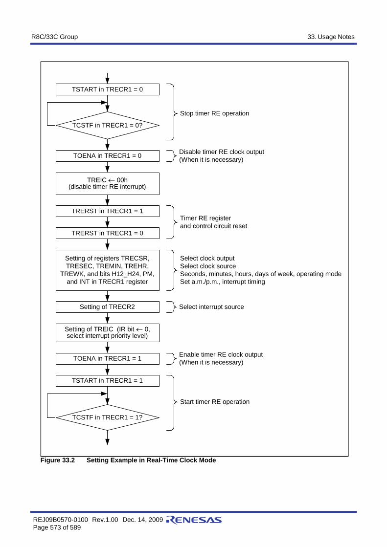
R8C/33C Group 33. Usage Notes
REJ09B0570-0100 Rev.1.00 Dec. 14, 2009Page 573 of 589
Figure 33.2 Setting Example in Real-Time Clock Mode
Stop timer RE operation
TCSTF in TRECR1 = 0?
TSTART in TRECR1 = 0
TRERST in TRECR1 = 1
TRERST in TRECR1 = 0
Setting of registers TRECSR,TRESEC, TREMIN, TREHR,
TREWK, and bits H12_H24, PM,and INT in TRECR1 register
Setting of TRECR2
TSTART in TRECR1 = 1
TCSTF in TRECR1 = 1?
TREIC ← 00h(disable timer RE interrupt)
Setting of TREIC (IR bit ← 0,select interrupt priority level)
Timer RE registerand control circuit reset
Select clock outputSelect clock sourceSeconds, minutes, hours, days of week, operating modeSet a.m./p.m., interrupt timing
Select interrupt source
Start timer RE operation
TOENA in TRECR1 = 0 Disable timer RE clock output(When it is necessary)
TOENA in TRECR1 = 1 Enable timer RE clock output(When it is necessary)

R8C/33C Group 33. Usage Notes
REJ09B0570-0100 Rev.1.00 Dec. 14, 2009Page 574 of 589
33.9.3 Time Reading Procedure of Real-Time Clock ModeIn real-time clock mode, read registers TRESEC, TREMIN, TREHR, and TREWK when time data is updatedand read the PM bit in the TRECR1 register when the BSY bit is set to 0 (not while data is updated). Also, when reading several registers, an incorrect time will be read if data is updated before another register isread after reading any register.
In order to prevent this, use the reading procedure shown below.
• Using an interruptRead necessary contents of registers TRESEC, TREMIN, TREHR, and TREWK and the PM bit in theTRECR1 register in the timer RE interrupt routine.
• Monitoring with a program 1Monitor the IR bit in the TREIC register with a program and read necessary contents of registers TRESEC,TREMIN, TREHR, and TREWK and the PM bit in the TRECR1 register after the IR bit in the TREIC registeris set to 1 (timer RE interrupt request generated).
• Monitoring with a program 2(1) Monitor the BSY bit.(2) Monitor until the BSY bit is set to 0 after the BSY bit is set to 1 (approximately 62.5 ms while the BSY bit
is set to 1).(3) Read necessary contents of registers TRESEC, TREMIN, TREHR, and TREWK and the PM bit in the
TRECR1 register after the BSY bit is set to 0.
• Using read results if they are the same value twice(1) Read necessary contents of registers TRESEC, TREMIN, TREHR, and TREWK and the PM bit in the
TRECR1 register.(2) Read the same register as (1) and compare the contents.(3) Recognize as the correct value if the contents match. If the contents do not match, repeat until the read
contents match with the previous contents.Also, when reading several registers, read them as continuously as possible.

R8C/33C Group 33. Usage Notes
REJ09B0570-0100 Rev.1.00 Dec. 14, 2009Page 575 of 589
33.10 Notes on Serial Interface (UARTi (i = 0 or 1))• When reading data from the UiRB (i = 0 or 1) register either in clock synchronous serial I/O mode or in clock
asynchronous serial I/O mode, always read data in 16-bit units. When the high-order byte of the UiRB register is read, bits PER and FER in the UiRB register and the RI bit inthe UiC1 register are set to 0.To check receive errors, read the UiRB register and then use the read data.
Program example to read the receive buffer register:MOV.W 00A6H,R0 ; Read the U0RB register
• When writing data to the UiTB register in clock asynchronous serial I/O mode with 9-bit transfer data length,write data to the high-order byte first and then the low-order byte, in 8-bit units.
Program example to write to the transmit buffer register:MOV.B #XXH,00A3H ; Write to the high-order byte of the U0TB registerMOV.B #XXH,00A2H ; Write to the low-order byte of the U0TB register

R8C/33C Group 33. Usage Notes
REJ09B0570-0100 Rev.1.00 Dec. 14, 2009Page 576 of 589
33.11 Notes on Serial Interface (UART2)
33.11.1 Clock Synchronous Serial I/O Mode
33.11.1.1 Transmission/ReceptionWhen the RTS function is used with an external clock, the RTS2 pin outputs “L,” which informs thetransmitting side that the MCU is ready for a receive operation. The RTS2 pin outputs “H” when a receiveoperation starts. Therefore, the transmit timing and receive timing can be synchronized by connecting the RTS2pin to the CTS2 pin of the transmitting side. The RTS function is disabled when an internal clock is selected.
33.11.1.2 TransmissionIf an external clock is selected, the following conditions must be met while the external clock is held high whenthe CKPOL bit in the U2C0 register is set to 0 (transmit data output at the falling edge and receive data input atthe rising edge of the transfer clock), or while the external clock is held low when the CKPOL bit is set to 1(transmit data output at the rising edge and receive data input at the falling edge of the transfer clock).• The TE bit in the U2C1 register = 1 (transmission enabled)• The TI bit in the U2C1 register = 0 (data present in the U2TB register)• If the CTS function is selected, input on the CTS2 pin = “L”
33.11.1.3 ReceptionIn clock synchronous serial I/O mode, the shift clock is generated by activating the transmitter. Set the UART2-associated registers for transmit operation even if the MCU is used for receive operation only. Dummy data isoutput from the TXD2 pin while receiving.
When an internal clock is selected, the shift clock is generated by setting the TE bit in the U2C1 register to 1(transmission enabled) and placing dummy data in the U2TB register. When an external clock is selected, setthe TE bit to 1 (transmission enabled), place dummy data in the U2TB register, and input an external clock tothe CLK2 pin to generate the shift clock.
If data is received consecutively, an overrun error occurs when the RE bit in the U2C1 register is set to 1 (datapresent in the U2RB register) and the next receive data is received in the UART2 receive register. Then, theOER bit in the U2RB register is set to 1 (overrun error). At this time, the U2RB register value is undefined. If anoverrun error occurs, the IR bit in the S2RIC register remains unchanged.
To receive data consecutively, set dummy data in the low-order byte in the U2TB register per each receiveoperation.
If an external clock is selected, the following conditions must be met while the external clock is held high whenthe CKPOL bit is set to 0, or while the external clock is held low when the CKPOL bit is set to 1.• The RE bit in the U2C1 register = 1 (reception enabled)• The TE bit in the U2C1 register = 1 (transmission enabled)• The TI bit in the U2C1 register = 0 (data present in the U2TB register)

R8C/33C Group 33. Usage Notes
REJ09B0570-0100 Rev.1.00 Dec. 14, 2009Page 577 of 589
33.11.2 Special Mode 1 (I2C Mode)When generating start, stop, and restart conditions, set the STSPSEL bit in the U2SMR4 register to 0 and waitfor more than half cycle of the transfer clock before changing each condition generation bit (STAREQ,RSTAREQ, and STPREQ) from 0 to 1.
33.12 Notes on Synchronous Serial Communication UnitSet the IICSEL bit in the SSUIICSR register to 0 (select SSU function) to use the synchronous serialcommunication unit function.
33.13 Notes on I2C bus InterfaceTo use the I2C bus interface, set the IICSEL bit in the SSUIICSR register to 1 (I2C bus interface functionselected).
33.14 Notes on Hardware LINFor the time-out processing of the header and response fields, use another timer to measure the duration of timewith a Synch Break detection interrupt as the starting point.
33.15 Notes on A/D Converter• Write to the ADMOD register, the ADINSEL register, the ADCON0 register (other than ADST bit), the
ADCON1 register, the OCVREFCR register when A/D conversion is stopped (before a trigger occurs).• To use the A/D converter in repeat mode 0, repeat mode 1, or repeat sweep mode, select the frequency of the A/D
converter operating clock φAD or more for the CPU clock during A/D conversion. Do not select fOCO-F as φAD.
• Connect 0.1 µF capacitor between the VREF pin and AVSS pin.• Do not enter stop mode during A/D conversion.• Do not enter wait mode during A/D conversion regardless of the state of the CM02 bit in the CM0 register (1:
Peripheral function clock stops in wait mode or 0: Peripheral function clock does not stop in wait mode). • Do not set the FMSTP bit in the FMR0 register to 1 (flash memory stops) or the FMR27 bit to 1 (low-current-
consumption read mode enabled) during A/D conversion. Otherwise, the A/D conversion result will beundefined.
• Do not change the CKS2 bit in the ADMOD register while fOCO-F is stopped.• During an A/D conversion operation, if the ADST bit in the ADCON0 register is set to 0 (A/D conversion stops)
by a program to forcibly terminate A/D conversion, the conversion result of the A/D converter is undefined andno interrupt is generated. The value of the ADi register before A/D conversion may also be undefined. If the ADST bit is set to 0 by a program, do not use the value of all the ADi register.

R8C/33C Group 33. Usage Notes
REJ09B0570-0100 Rev.1.00 Dec. 14, 2009Page 578 of 589
33.16 Notes on Flash Memory
33.16.1 CPU Rewrite Mode
33.16.1.1 Prohibited InstructionsThe following instructions cannot be used while the program ROM area is being rewritten in EW0 modebecause they reference data in the flash memory: UND, INTO, and BRK.
33.16.1.2 InterruptsTables 33.1 and 33.3 show CPU Rewrite Mode Interrupts (1), (2) and (3), respectively.
FMR21, FMR22: Bits in FMR2 register
Table 33.1 CPU Rewrite Mode Interrupts (1)
ModeErase/Write Target
Status Maskable Interrupt
EW0 Data flash
During auto-erasure(suspend enabled)
When an interrupt request is acknowledged, interrupt handling is executed. If the FMR22 bit is set to 1 (erase-suspend request enabled by interrupt request), the FMR21 bit is automatically set to 1 (erase-suspend request). The flash memory suspends auto-erasure after td(SR-SUS). If erase-suspend is required while the FMR22 bit is set to 0 (erase-suspend request disabled by interrupt request), set the FMR21 bit to 1 during interrupt handling. The flash memory suspends auto-erasure after td(SR-SUS).While auto-erasure is being suspended, any block other than the block during auto-erasure execution can be read or written. Auto-erasure can be restarted by setting the FMR21 bit to 0 (erase restart).
During auto-erasure(suspend disabled or FMR22 = 0)
Interrupt handling is executed while auto-erasure or auto-programming is being performed.
During auto-programming
Program ROM
During auto-erasure(suspend enabled)
Usable by allocating a vector in RAM.
During auto-erasure(suspend disabled)During auto-programming
EW1 Data flash
During auto-erasure(suspend enabled)
When an interrupt request is acknowledged, interrupt handling is executed. If the FMR22 bit is set to 1, the FMR21 bit is automatically set to 1. The flash memory suspends auto-erasure after td(SR-SUS). If erase-suspend is required while the FMR22 bit is set to 0, set the FMR21 bit to 1 during interrupt handling. The flash memory suspends auto-erasure after td(SR-SUS).While auto-erasure is being suspended, any block other than the block during auto-erasure execution can be read or written. Auto-erasure can be restarted by setting the FMR21 bit to 0.
During auto-erasure(suspend disabled or FMR22 = 0)
Interrupt handling is executed while auto-erasure or auto-programming is being performed.
During auto-programming
Program ROM
During auto-erasure(suspend enabled)
Auto-erasure suspends after td(SR-SUS) and interrupt handling is executed. Auto-erasure can be restarted by setting the FMR21 bit to 0 after interrupt handling completes. While auto-erasure is being suspended, any block other than the block during auto-erasure execution can be read or written.
During auto-erasure(suspend disabled or FMR22 = 0)
Auto-erasure and auto-programming have priority and interrupt requests are put on standby. Interrupt handling is executed after auto-erase and auto-program complete.
During auto-programming

R8C/33C Group 33. Usage Notes
REJ09B0570-0100 Rev.1.00 Dec. 14, 2009Page 579 of 589
FMR21, FMR22: Bits in FMR2 registerNote:
1. Do not use a non-maskable interrupt while block 0 is being auto-erased because the fixed vector is allocated in block 0.
Table 33.2 CPU Rewrite Mode Interrupts (2)
ModeErase/Write Target
Status
• Watchdog Timer• Oscillation Stop Detection• Voltage Monitor 2• Voltage Monitor 1• NMI (Note 1)
• Undefined Instruction• INTO Instruction• BRK Instruction• Single Step• Address Match• Address Break (Note 1)
EW0 Data flash During auto-erasure(suspend enabled)
When an interrupt request is acknowledged, interrupt handling is executed. If the FMR22 bit is set to 1 (erase-suspend request enabled by interrupt request), the FMR21 bit is automatically set to 1 (erase-suspend request). The flash memory suspends auto-erasure after td(SR-SUS). If erase-suspend is required while the FMR22 bit is set to 0 (erase-suspend request disabled by interrupt request), set the FMR21 bit to 1 during interrupt handling. The flash memory suspends auto-erasure after td(SR-SUS).While auto-erasure is being suspended, any block other than the block during auto-erasure execution can be read or written. Auto-erasure can be restarted by setting the FMR21 bit is set to 0 (erase restart).
When an interrupt request is acknowledged, interrupt handling is executed.If erase-suspend is required, set the FMR21 bit to 1 during interrupt handling. The flash memory suspends auto-erasure after td(SR-SUS).While auto-erasure is being suspended, any block other than the block during auto-erasure execution can be read or written. Auto-erasure can be restarted by setting the FMR21 bit in the FMR2 register is set to 0 (erase restart).
During auto-erasure(suspend disabled or FMR22 = 0)
Interrupt handling is executed while auto-erasure or auto-programming is being performed.
During auto-programming
Program ROM
During auto-erasure(suspend enabled)
When an interrupt request is acknowledged, auto-erasure or auto-programming is forcibly stopped immediately and the flash memory is reset. Interrupt handling starts when the flash memory restarts after the fixed period. Since the block during auto-erasure or the address during auto-programming is forcibly stopped, the normal value may not be read. After the flash memory restarts, execute auto-erasure again and ensure it completes normally. The watchdog timer does not stop during the command operation, so interrupt requests may be generated. Initialize the watchdog timer regularly using the erase-suspend function.
Not usable during auto-erasure or auto-programming.
During auto-erasure(suspend disabled)During auto-programming

R8C/33C Group 33. Usage Notes
REJ09B0570-0100 Rev.1.00 Dec. 14, 2009Page 580 of 589
FMR21, FMR22: Bits in FMR2 registerNote:
1. Do not use a non-maskable interrupt while block 0 is being auto-erased because the fixed vector is allocated in block 0.
Table 33.3 CPU Rewrite Mode Interrupts (3)
ModeErase/Write Target
Status
• Watchdog Timer• Oscillation Stop Detection• Voltage Monitor 2• Voltage Monitor 1• NMI (Note 1)
• Undefined Instruction• INTO Instruction• BRK Instruction• Single Step• Address Match• Address Break (Note 1)
EW1 Data flash During auto-erasure(suspend enabled)
When an interrupt request is acknowledged, interrupt handling is executed. If the FMR22 bit is set to 1, the FMR21 bit is automatically set to 1. The flash memory suspends auto-erasure after td(SR-SUS). If erase-suspend is required while the FMR22 bit is set to 0, set the FMR21 bit to 1 during interrupt handling. The flash memory suspends auto-programming after td(SR-SUS).While auto-erasure is being suspended, any block other than the block during auto-erasure execution can be read or written. Auto-erasure can be restarted by setting the FMR21 bit is set to 0.
When an interrupt request is acknowledged, interrupt handling is executed.If erase-suspend is required, set the FMR21 bit to 1 during interrupt handling. The flash memory suspends auto-erasure after td(SR-SUS).While auto-erasure is being suspended, any block other than the block during auto-erasure execution can be read or written. Auto-erasure can be restarted by setting the FMR21 bit in the FMR2 register is set to 0 (erase restart).
During auto-erasure(suspend disabled or FMR22 = 0)
Interrupt handling is executed while auto-erasure or auto-programming is being performed.
During auto-programming
Program ROM
During auto-erasure(suspend enabled)
When an interrupt request is acknowledged, auto-erasure or auto-programming is forcibly stopped immediately and the flash memory is reset. Interrupt handling starts when the flash memory restarts after the fixed period. Since the block during auto-erasure or the address during auto-programming is forcibly stopped, the normal value may not be read. After the flash memory restarts, execute auto-erasure again and ensure it completes normally. The watchdog timer does not stop during the command operation, so interrupt requests may be generated. Initialize the watchdog timer regularly using the erase-suspend function.
Not usable during auto-erasure orauto-programming.
During auto-erasure(suspend disabled or FMR22 = 0)During auto-programming

R8C/33C Group 33. Usage Notes
REJ09B0570-0100 Rev.1.00 Dec. 14, 2009Page 581 of 589
33.16.1.3 How to AccessTo set one of the following bits to 1, first write 0 and then 1 immediately. Disable interrupts and DTC activationbetween writing 0 and writing 1.• The FMR01 bit or FMR02 bit in the FMR0 register• The FMR13 bit in the FMR1 register• The FMR20 bit, FMR22 bit, or FMR 27 bit in the FMR2 register
To set one of the following bits to 0, first write 1 and then 0 immediately. Disable interrupts and DTC activationbetween writing 0 and writing 1.• The FMR14 bit, FMR15 bit, FMR16 bit, or FMR17 bit in the FMR1 register
33.16.1.4 Rewriting User ROM AreaIn EW0 Mode, if the supply voltage drops while rewriting any block in which a rewrite control program isstored, it may not be possible to rewrite the flash memory because the rewrite control program cannot berewritten correctly. In this case, use standard serial I/O mode.
33.16.1.5 ProgrammingDo not write additions to the already programmed address.
33.16.1.6 Entering Stop Mode or Wait ModeDo not enter stop mode or wait mode during erase-suspend.If the FST7 in the FST register is set to 0 (busy (during programming or erasure execution)), do not enter to stopmode or wait mode.Do not enter stop mode or wait mode while the FMR27 bit is 1 (low-current-consumption read mode enabled).
33.16.1.7 Programming and Erasure Voltage for Flash MemoryTo perform programming and erasure, use VCC = 2.7 V to 5.5 V as the supply voltage. Do not performprogramming and erasure at less than 2.7 V.
33.16.1.8 Block Blank CheckDo not execute the block blank check command during erase-suspend.
33.16.1.9 Low-Current-Consumption Read ModeIn low-speed clock mode and low-speed on-chip oscillator mode, the current consumption when reading theflash memory can be reduced by setting the FMR27 bit in the FMR2 register to 1 (low-current-consumptionread mode enabled).Low-current-consumption read mode can be used when the CPU clock is set to either of the following:• The CPU clock is set to the low-speed on-chip oscillator clock divided by 4, 8, or 16.• The CPU clock is set to the XCIN clock divided by 1 (no division), 2, 4, or 8.However, do not use low-current-consumption read mode when the frequency of the selected CPU clock is3 kHz or below. After setting the divide ratio of the CPU clock, set the FMR27 bit to 1 (low-current-consumption read mode enabled).To reduce the power consumption, refer to 31. Reducing Power Consumption.Enter wait mode or stop mode after setting the FMR27 bit to 0 (low-current-consumption read mode disabled).Do not enter wait mode or stop mode while the FMR27 bit is 1 (low-current-consumption read mode enabled).

R8C/33C Group 33. Usage Notes
REJ09B0570-0100 Rev.1.00 Dec. 14, 2009Page 582 of 589
33.17 Notes on Noise
33.17.1 Inserting a Bypass Capacitor between VCC and VSS Pins as a Countermeasureagainst Noise and Latch-up
Connect a bypass capacitor (at least 0.1 µF) using the shortest and thickest wire possible.
33.17.2 Countermeasures against Noise Error of Port Control RegistersDuring rigorous noise testing or the like, external noise (mainly power supply system noise) can exceed thecapacity of the MCU’s internal noise control circuitry. In such cases the contents of the port related registersmay be changed.As a firmware countermeasure, it is recommended that the port registers, port direction registers, and pull-upcontrol registers be reset periodically. However, examine the control processing fully before introducing thereset routine as conflicts may be created between the reset routine and interrupt routines.

R8C/33C Group 34. Notes on On-Chip Debugger
REJ09B0570-0100 Rev.1.00 Dec. 14, 2009Page 583 of 589
34. Notes on On-Chip DebuggerWhen using the on-chip debugger to develop and debug programs for the R8C/33C Group, take note of the following:
(1) Some of the user flash memory and RAM areas are used by the on-ship debugger. These areas cannot be accessedby the user.Refer to the on-chip debugger manual for which areas are used.
(2) Do not set the address match interrupt (registers AIER0, AIER1, RMAD0, and RMAD1 and fixed vector tables)in a user system.
(3) Do not use the BRK instruction in a user system.(4) Debugging is available under the condition of supply voltage VCC = 1.8 to 5.5 V. Set the supply voltage to 2.7 V
or above for rewriting the flash memory.
Connecting and using the on-chip debugger has some special restrictions. Refer to the on-chip debugger manual fordetails.

R8C/33C Group 35. Notes on Emulator Debugger
REJ09B0570-0100 Rev.1.00 Dec. 14, 2009Page 584 of 589
35. Notes on Emulator DebuggerConnecting and using the emulator debugger has some special restrictions. Refer to the emulator debugger manual fordetails.

R8C/33C Group Appendix 1. Package Dimensions
REJ09B0570-0100 Rev.1.00 Dec. 14, 2009Page 585 of 589
Appendix 1. Package DimensionsDiagrams showing the latest package dimensions and mounting information are available in the “Packages” section ofthe Renesas Technology website.
2.
1. DIMENSIONS "*1" AND "*2"DO NOT INCLUDE MOLD FLASH.
NOTE)
DIMENSION "*3" DOES NOTINCLUDE TRIM OFFSET.
y
Index mark
*3
F
32
25
24 17
16
9
81
*1
*2
xbpe
HEE
D
HD
ZD
ZE
Detail F
L1
L
A
cA2
A1
Previous CodeJEITA Package Code RENESAS Code
PLQP0032GB-A 32P6U-A
MASS[Typ.]
0.2gP-LQFP32-7x7-0.80
1.0
0.125
0.35
0.7
0.7
0.20
0.200.1450.09
0.420.370.32
MaxNomMin
Dimension in MillimetersSymbol
Reference
7.17.06.9D
7.17.06.9E
1.4A2
9.29.08.8
9.29.08.8
1.7A
0.20.10
0.70.50.3L
x
8°0°
c
0.8e
0.10y
HD
HE
A1
bp
b1
c1
ZD
ZE
L1
Terminal cross section
b1
c 1
bp
c

R8C/33C Group Appendix 2. Connection Examples between Serial Writer and On-Chip Debugging Emulator
REJ09B0570-0100 Rev.1.00 Dec. 14, 2009Page 586 of 589
Appendix 2. Connection Examples between Serial Writer and On-ChipDebugging Emulator
Appendix Figure 2.1 shows a Connection Example with M16C Flash Starter (M3A-0806) and Appendix Figure 2.2shows a Connection Example with E8a Emulator (R0E00008AKCE00).
Appendix Figure 2.1 Connection Example with M16C Flash Starter (M3A-0806)
Appendix Figure 2.2 Connection Example with E8a Emulator (R0E00008AKCE00)
Note: 1. An oscillation circuit must be connected, even when operating with the on-chip oscillator clock.
RXD 4
7 VSS
1 VCC
10
M16C Flash Starter(M3A-0806)
RXD
TXD
VSS
VCC
TXD
RESETConnect
oscillationcircuit (1)
29 28 27 26 2532 31 30
9 10 11 12 13 14 15 16
5
7
8
1
2
3
4
6
24
23
22
21
20
19
18
17
R8C
/33C G
roup
MODE
Note: 1. It is not necessary to connect an oscillation circuit when
operating with the on-chip oscillator clock.
MODE
4.7kΩ ±10%
E8a emulator(R0E00008AKCE00)
RESET12
10
8
6
4
2VSS
13
7 MODE
VCC
14
VSS
VCC
Connectoscillation
circuit (1)
29 28 27 26 2532 31 30
9 10 11 12 13 14 15 16
5
7
8
1
2
3
4
6
24
23
22
21
20
19
18
17
R8C
/33C G
roup
4.7kΩ or more
Open collector buffer
User logic

R8C/33C Group Appendix 3. Example of Oscillation Evaluation Circuit
REJ09B0570-0100 Rev.1.00 Dec. 14, 2009Page 587 of 589
Appendix 3. Example of Oscillation Evaluation CircuitAppendix Figure 3.1 shows an Example of Oscillation Evaluation Circuit.
Appendix Figure 3.1 Example of Oscillation Evaluation Circuit
Connectoscillationcircuit
Note:1. After reset, the XIN and XCIN clocks are stopped.
Write a program to oscillate the XIN and XCIN clocks.
VSS
VCC
RESET
29 28 27 26 2532 31 30
9 10 11 12 13 14 15 16
5
7
8
1
2
3
4
6
24
23
22
21
20
19
18
17
R8C
/33C G
roup

REJ09B0570-0100 Rev.1.00 Dec. 14, 2009Page 588 of 589
R8C/33C Group Index
[ A ]ADCON0 ............................................................................. 462ADCON1 ............................................................................. 463ADi (i = 0 to 7) ..................................................................... 459ADIC .................................................................................... 137ADINSEL ............................................................................. 461ADMOD ............................................................................... 460AIERi (i = 0 or 1) .................................................................. 153
[ C ]CM0 ..................................................................................... 102CM1 ..................................................................................... 103CM3 ..................................................................................... 104CMPA .................................................................................... 41CPSRF ................................................................................ 107CSPR .................................................................................. 170
[ D ]DACON ............................................................................... 482DAi (i = 0 or 1) ..................................................................... 482DRR0 .................................................................................... 79DRR1 .................................................................................... 80DTBLSj (j = 0 to 23) ............................................................. 178DTCCRj (j = 0 to 23) ............................................................ 178DTCCTj (j = 0 to 23) ............................................................ 179DTCENi (i = 0 to 3, 5, 6) ...................................................... 180DTCTL ................................................................................. 181DTDARj (j = 0 to 23) ............................................................ 179DTRLDj (j = 0 to 23) ............................................................ 179DTSARj (j = 0 to 23) ............................................................ 179
[ F ]FMR0 .................................................................................. 497FMR1 .................................................................................. 499FMR2 .................................................................................. 501FMRDYIC ............................................................................ 138FRA0 ................................................................................... 106FRA1 ................................................................................... 106FRA2 ................................................................................... 107FRA3 ................................................................................... 108FRA4 ................................................................................... 108FRA5 ................................................................................... 108FRA6 ................................................................................... 108FRA7 ................................................................................... 105FST ..................................................................................... 495
[ I ]ICCR1 ................................................................................. 410ICCR2 ................................................................................. 411ICDRR ................................................................................. 409ICDRS ................................................................................. 415ICDRT ................................................................................. 409ICIER ................................................................................... 413ICMR ................................................................................... 412ICSR .................................................................................... 414INTCMP .............................................................................. 485INTEN ......................................................................... 148, 485INTF ............................................................................ 148, 486INTiIC (i = 0, 1, 3) ................................................................ 139INTSR ........................................................................... 75, 147
[ K ]KIEN .................................................................................... 151KUPIC .................................................................................. 137
[ L ]LINCR .................................................................................. 444LINCR2 ................................................................................ 443LINST .................................................................................. 444
[ M ]MSTCR ................................................................ 239, 374, 406
[ O ]OCD ..................................................................................... 105OCVREFCR ........................................................................ 458OFS ......................................................... 29, 48, 164, 171, 493OFS2 ..................................................................... 30, 165, 172
[ P ]P1DRR .................................................................................. 78P2DRR .................................................................................. 78PDi (i = 0 to 4) ....................................................................... 68Pi (i = 0 to 4) .......................................................................... 69PINSR ............................................................................ 76, 408PM0 ....................................................................................... 28PM1 ..................................................................................... 169PRCR .................................................................................. 131PUR0 ..................................................................................... 77PUR1 ..................................................................................... 77
[ R ]RMADi (i = 0 or 1) ................................................................ 153RSTFR ................................................................................... 28
[ S ]S0RIC .................................................................................. 137S0TIC .................................................................................. 137S1RIC .................................................................................. 137S1TIC .................................................................................. 137S2RIC .................................................................................. 137S2TIC .................................................................................. 137SAR ..................................................................................... 415SSBR ................................................................................... 376SSCRH ................................................................................ 377SSCRL ................................................................................. 378SSER ................................................................................... 380SSMR .................................................................................. 379SSMR2 ................................................................................ 382SSRDR ................................................................................ 377SSSR ................................................................................... 381SSTDR ................................................................................ 376SSUIC/IICIC ........................................................................ 138SSUIICSR .............................................................. 75, 375, 407
[ T ]TRA ..................................................................................... 202TRACR ................................................................................ 200TRAIC .................................................................................. 137TRAIOC ....................................... 200, 203, 206, 208, 210, 213TRAMR ................................................................................ 201TRAPRE .............................................................................. 201
Index

REJ09B0570-0100 Rev.1.00 Dec. 14, 2009Page 589 of 589
R8C/33C Group Index
TRASR .......................................................................... 70, 202TRBCR ................................................................................ 217TRBIC ................................................................................. 137TRBIOC ............................................... 218, 221, 225, 228, 232TRBMR ............................................................................... 218TRBOCR ............................................................................. 217TRBPR ................................................................................ 220TRBPRE .............................................................................. 219TRBRCSR ............................................................. 70, 220, 246TRBSC ................................................................................ 219TRC ..................................................................................... 243TRCADCR ........................................................................... 245TRCCR1 ...................................................... 240, 262, 271, 277TRCCR2 ...................................................... 244, 265, 271, 278TRCDF ........................................................................ 244, 278TRCGRA ............................................................................. 243TRCGRB ............................................................................. 243TRCGRC ............................................................................. 243TRCGRD ............................................................................. 243TRCIC ................................................................................. 138TRCIER ............................................................................... 240TRCIOR0 ............................................................ 242, 257, 263TRCIOR1 ............................................................ 242, 258, 264TRCMR ............................................................................... 239TRCOER ............................................................................. 245TRCPSR0 ..................................................................... 71, 247TRCPSR1 ..................................................................... 72, 248TRCSR ................................................................................ 241TRECR1 ...................................................................... 291, 298TRECR2 ...................................................................... 292, 298TRECSR ..................................................................... 293, 299TREHR ................................................................................ 290TREIC ................................................................................. 137TREMIN ...................................................................... 289, 297TRESEC ...................................................................... 289, 297TREWK ............................................................................... 290
[ U ]U0SR ............................................................................. 73, 310U1SR ............................................................................. 73, 310U2BCNIC ............................................................................ 137U2BRG ................................................................................ 328U2C0 ................................................................................... 330U2C1 ................................................................................... 331U2MR .................................................................................. 328U2RB ................................................................................... 332U2SMR ................................................................................ 335U2SMR2 .............................................................................. 335U2SMR3 .............................................................................. 334U2SMR4 .............................................................................. 334U2SMR5 .............................................................................. 333U2SR0 ........................................................................... 74, 336U2SR1 ........................................................................... 74, 336U2TB ................................................................................... 329UiBRG (i = 0 or 1) ................................................................ 306UiC0 (i = 0 or 1) ................................................................... 308UiC1 (i = 0 or 1) ................................................................... 308UiMR (i = 0 or 1) .................................................................. 306UiRB (i = 0 or 1) .................................................................. 309UiTB (i = 0 or 1) ................................................................... 307URXDF ................................................................................ 333
[ V ]VCA1 ..................................................................................... 42VCA2 ............................................................................. 43, 109
VCAC ..................................................................................... 42VCMP1IC ............................................................................. 137VCMP2IC ............................................................................. 137VD1LS ................................................................................... 44VLT0 ...................................................................................... 81VLT1 ...................................................................................... 82VW0C .................................................................................... 45VW1C .................................................................................... 46VW2C .................................................................................... 47
[ W ]WDTC .................................................................................. 170WDTR .................................................................................. 169WDTS .................................................................................. 169

C - 1
REVISION HISTORY R8C/33C Group Hardware Manual
Rev. DateDescription
Page Summary0.10 Sep. 17, 2009 — First Edition issued1.00 Dec. 14, 2009 All “Preliminary” and “Under development” deleted
4 Table 1.3 revised43, 45,
1096.2.4, 6.2.6, 9.2.14 revised
47 6.2.8 b7 “or LVCMP2” deleted54 Figure 6.7 “VCC or LVCMP2” → “VCC”66 Figure 7.10 revised
104 9.2.3 Note5 deleted114 9.6.5 “VCC = 3.0 to 5.5 V” → “VCC = 2.7 to 5.5 V”118 9.7.2.2 revised122 9.7.3.1 revised
129, 560 9.9.1, 9.9.2, 33.1.1, 33.1.2 revised170 14.2.5 revised180 15.2.7 Note1 added299 20.3.5 b2 “(1)” added, Note1 revised326 Figure 22.1 revised456 Table 27.1 Note2 revised494 Table 30.3 CPU clock: “20 MHz” → “Max. 20 MHz”
501, 502 30.4.4 Note3, FMR27 Bit revised527, 581 30.7.1.6, 30.7.1.9, 33.16.1.6, 33.16.1.9 revised
531 31.2.11, Figure 31.3 Note2 revised536 Table 32.3 revised538 Table 32.6 revised539 Table 32.7 revised540 Table 32.8, Table 32.9 revised541 Table 32.10 revised542 Table 32.12 revised, Note2 deleted
R8C/33C Group Hardware ManualREVISION HISTORY

R8C/33C Group Hardware Manual
Publication Date: Rev.0.10 Sep. 17, 2009 Rev.1.00 Dec. 14, 2009
Published by: Sales Strategic Planning Div.Renesas Technology Corp.
© 2009. Renesas Technology Corp., All rights reserved. Printed in Japan

1753, Shimonumabe, Nakahara-ku, Kawasaki-shi, Kanagawa 211-8668 Japan
R8C/33C Group
REJ09B0570-0100
Hardware Manual