odin-w2 series - tme.eu€¦ · stand-alone multiradio modules with wi-fi and bluetooth ... 10...
TRANSCRIPT
ODIN-W2 series Stand-alone multiradio modules with Wi-Fi and Bluetooth® Data Sheet
www.u-blox.com
UBX-14039949 - R13
Abstract
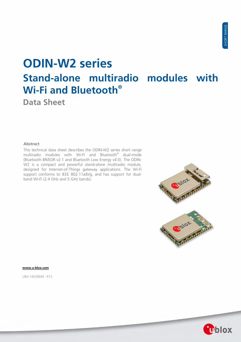
This technical data sheet describes the ODIN-W2 series short range multiradio modules with Wi-Fi and Bluetooth® dual-mode (Bluetooth BR/EDR v2.1 and Bluetooth Low Energy v4.0). The ODIN-W2 is a compact and powerful stand-alone multiradio module, designed for Internet-of-Things gateway applications. The Wi-Fi support conforms to IEEE 802.11a/b/g, and has support for dual-band Wi-Fi (2.4 GHz and 5 GHz bands).
ODIN-W2 series - Data Sheet
UBX-14039949 - R13 Page 2 of 44
Document Information
Title ODIN-W2 series
Subtitle Stand-alone multiradio modules with Wi-Fi and Bluetooth®
Document type Data Sheet
Document number UBX-14039949
Revision and date R13 1-Sep-2017
Disclosure restriction
Product Status Corresponding content status
Functional Sample Draft For functional testing. Revised and supplementary data will be published later.
In Development / Prototype
Objective Specification Target values. Revised and supplementary data will be published later.
Engineering Sample Advance Information Data based on early testing. Revised and supplementary data will be published later.
Initial Production Early Prod. Information Data from product verification. Revised and supplementary data may be published later.
Mass Production / End of Life Production Information Final product specification.
This document applies to the following products:
Product name Type number Software version PCN reference Product status
ODIN-W260 ODIN-W260-00B-00 1.0.0 N/A Mass Production
ODIN-W260-01B-00 2.0.0
ODIN-W260-01B-01 2.0.1 2.0.2
ODIN-W260-02B-00 3.0.0 3.0.1
ODIN-W260-03B-00 4.0.0
ODIN-W260-03B-01 ODIN-W260-03X-00
4.0.1
ODIN-W262 ODIN-W262-00B-00 1.0.0 N/A Mass Production
ODIN-W262-01B-00 2.0.0
ODIN-W262-01B-01 2.0.1 2.0.2
ODIN-W262-02B-00 3.0.0 3.0.1
ODIN-W262-03B-00 4.0.0
ODIN-W262-03B-01 ODIN-W262-03X-00
4.0.1
u-blox reserves all rights to this document and the information contained herein. Products, names, logos and designs described herein may in whole or in part be subject to intellectual property rights. Reproduction, use, modification or disclosure to third parties of this document or any part thereof without the express permission of u-blox is strictly prohibited.
The information contained herein is provided “as is” and u-blox assumes no liability for the use of the information. No warranty, either express or implied, is given, including but not limited, with respect to the accuracy, correctness, reliability and fitness for a particular purpose of the information. This document may be revised by u-blox at any time. For most recent documents, visit www.u-blox.com.
Copyright © 2017, u-blox AG.
u-blox is a registered trademark of u-blox Holding AG in the EU and other countries. Arm® is the registered trademark of Arm Limited in the EU and other countries.
ODIN-W2 series - Data Sheet
UBX-14039949 - R13 Contents
Page 3 of 44
Contents Contents .............................................................................................................................. 3
1 Functional description .................................................................................................. 6 1.1 Overview .............................................................................................................................................. 6 1.2 Applications .......................................................................................................................................... 6 1.3 Product features ................................................................................................................................... 6 1.4 Block diagram ....................................................................................................................................... 7 1.5 Product description ............................................................................................................................... 8 1.6 AT command support ........................................................................................................................... 8 1.7 IEEE 802.11d and additional regulatory domains .................................................................................. 8
1.7.1 ODIN-W2 IEEE 802.11d implementation description ...................................................................... 9 1.8 MAC addresses ................................................................................................................................... 10
2 Interfaces .................................................................................................................... 11 2.1 Power management ........................................................................................................................... 11
2.1.1 Module supply input (VCC) ......................................................................................................... 11 2.1.2 Digital I/O interfaces supply output (V_INT) .................................................................................. 11
2.2 Antenna interfaces ............................................................................................................................. 11 2.2.1 Antenna connectors and internal antenna ................................................................................... 11
2.3 Data communication interfaces .......................................................................................................... 12 2.3.1 UART interface ............................................................................................................................ 12 2.3.2 Ethernet interface ........................................................................................................................ 12
3 System functions ........................................................................................................ 14 3.1 Module power modes ........................................................................................................................ 14 3.2 Module reset ...................................................................................................................................... 14 3.3 System IO ........................................................................................................................................... 14
4 Pin definition .............................................................................................................. 15 4.1 Pin assignment ................................................................................................................................... 15
5 Electrical specification ................................................................................................ 18 5.1 Absolute maximum ratings ................................................................................................................. 18
5.1.1 Maximum ESD ............................................................................................................................. 18 5.2 Operating conditions .......................................................................................................................... 18
5.2.1 Temperature range ...................................................................................................................... 18 5.2.2 Power supply ............................................................................................................................... 18 5.2.3 I/O DC characteristics .................................................................................................................. 19 5.2.4 Reset characteristics .................................................................................................................... 19 5.2.5 LPO clock .................................................................................................................................... 19 5.2.6 Universal asynchronous serial interface (UART) ............................................................................ 19
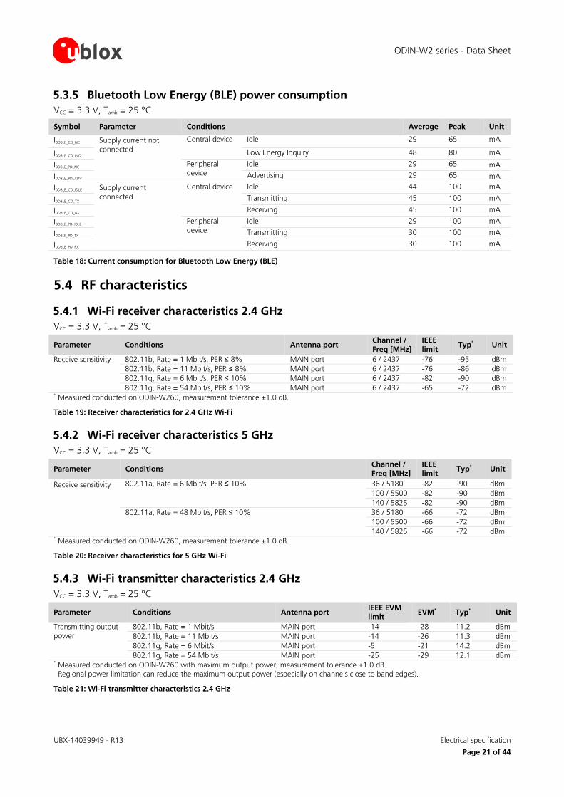
5.3 Power consumption ............................................................................................................................ 20
ODIN-W2 series - Data Sheet
UBX-14039949 - R13 Contents
Page 4 of 44
5.3.1 General power consumption ....................................................................................................... 20 5.3.2 Wi-Fi 2.4 GHz power consumption .............................................................................................. 20 5.3.3 Wi-Fi 5 GHz power consumption ................................................................................................. 20 5.3.4 Classic Bluetooth power consumption ......................................................................................... 20 5.3.5 Bluetooth Low Energy (BLE) power consumption ......................................................................... 21
5.4 RF characteristics ................................................................................................................................ 21 5.4.1 Wi-Fi receiver characteristics 2.4 GHz .......................................................................................... 21 5.4.2 Wi-Fi receiver characteristics 5 GHz ............................................................................................. 21 5.4.3 Wi-Fi transmitter characteristics 2.4 GHz ..................................................................................... 21 5.4.4 Wi-Fi transmitter characteristics 5 GHz ........................................................................................ 22 5.4.5 Classic Bluetooth receiver characteristics ..................................................................................... 22 5.4.6 Bluetooth Low Energy receiver sensitivity ..................................................................................... 22 5.4.7 Classic Bluetooth transmitter characteristics ................................................................................ 22 5.4.8 Bluetooth Low Energy transmitter characteristics ......................................................................... 22
6 Mechanical specifications .......................................................................................... 23 6.1 Dimensions ......................................................................................................................................... 23 6.2 Module weight ................................................................................................................................... 24
7 Qualification and approvals ...................................................................................... 25 7.1 Compliance with RoHS directive ......................................................................................................... 25 7.2 European Union regulatory compliance .............................................................................................. 25 7.3 Safety compliance ............................................................................................................................... 25 7.4 FCC and IC Compliance ...................................................................................................................... 25
7.4.1 IC compliance.............................................................................................................................. 25 7.4.2 Conformité aux normes d’IC ....................................................................................................... 25 7.4.3 FCC statement ............................................................................................................................ 26 7.4.4 Labeling requirements for end product ........................................................................................ 27
7.5 Japan radio equipment compliance ..................................................................................................... 28 7.6 SRRC China Radio Transmission Equipment Type Approval ................................................................. 28
7.6.1 ODIN-W262 labeling requirements for end product ..................................................................... 28 7.7 NCC Taiwan compliance ..................................................................................................................... 29
7.7.1 Taiwan NCC Warning Statement ................................................................................................. 29 7.7.2 ODIN-W260 labeling requirements for end product ..................................................................... 29 7.7.3 ODIN-W262 labeling requirements for end product ..................................................................... 29
7.8 Korean KCC certification .................................................................................................................... 30 7.9 Brazil compliance ................................................................................................................................ 30 7.10 Australia and New Zealand regulatory compliance .......................................................................... 30 7.11 South Africa regulatory compliance................................................................................................. 31 7.12 Bluetooth qualification information ................................................................................................. 31 7.13 ATEX Certification ........................................................................................................................... 31
8 Antennas ..................................................................................................................... 33 8.1 Antenna accessories ........................................................................................................................... 33 8.2 Approved antennas ............................................................................................................................ 34
ODIN-W2 series - Data Sheet
UBX-14039949 - R13 Contents
Page 5 of 44
8.2.1 Single band antennas .................................................................................................................. 34 8.2.2 Dual-band antennas .................................................................................................................... 36
9 Product handling and soldering ................................................................................ 37 9.1 Packaging ........................................................................................................................................... 37 9.2 Packaging ........................................................................................................................................... 37
9.2.1 Reels ........................................................................................................................................... 37 9.2.2 Tapes .......................................................................................................................................... 37
9.3 Moisture sensitivity levels .................................................................................................................... 38 9.4 Reflow soldering ................................................................................................................................. 38 9.5 ESD precautions .................................................................................................................................. 38
10 Labeling and ordering information ........................................................................... 39 10.1 Label information ............................................................................................................................ 39 10.2 Explanation of codes ....................................................................................................................... 40 10.3 Ordering information ...................................................................................................................... 41
Appendix .......................................................................................................................... 42
Glossary ............................................................................................................................ 42
Related documents........................................................................................................... 43
Revision history ................................................................................................................ 43
Contact .............................................................................................................................. 44
ODIN-W2 series - Data Sheet
UBX-14039949 - R13 Functional description
Page 6 of 44
1 Functional description
1.1 Overview The ODIN-W2 series is a highly integrated multiradio module developed by u-blox for integration in demanding, reliable devices such as those needed for industrial and medical applications. The module is built around a multiradio chip, which includes dual-band Wi-Fi and dual-mode Bluetooth (Classic Bluetooth v2.1+EDR and Bluetooth Low Energy v4.0). The Wi-Fi support conforms to IEEE 802.11a/b/g/n, and has support for dual-band 2.4 GHz and 5 GHz operation and 2.4 GHz 2×2 MIMO.
The high performance ODIN-W2 series module is available in different versions (see Product features). The module has a small form factor and the interface layout is the same as previous Bluetooth and Wi-Fi modules from u-blox in the 15x22 mm ODIN form factor.
The module is complete with embedded driver, stack and application for wireless data transfer and AT-command configuration.
1.2 Applications • Internet of Things (IoT) • Wi-Fi and Bluetooth networks • Medical and industrial networking • Access to laptops, mobile phones, and similar consumer devices • Home/building automation • Ethernet/Wireless Gateway
1.3 Product features
Table 1: Key features of ODIN-W2 series
ODIN-W2 series - Data Sheet
UBX-14039949 - R13 Functional description
Page 7 of 44
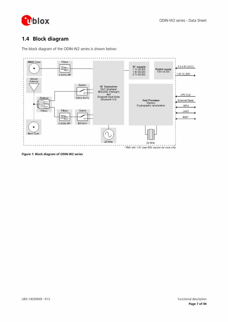
1.4 Block diagram
The block diagram of the ODIN-W2 series is shown below:
Figure 1: Block diagram of ODIN-W2 series
ODIN-W2 series - Data Sheet
UBX-14039949 - R13 Functional description
Page 8 of 44
1.5 Product description The ODIN-W2 series module supports Wi-Fi, classic Bluetooth and Bluetooth Low Energy (dual-mode / Bluetooth Smart Ready). The Wi-Fi support conforms to IEEE 802.11a/b/g/n, and has support for dual-band 2.4 GHz and 5 GHz operations and 2×2 MIMO (2.4 GHz).Wi-Fi
Classic Bluetooth
Bluetooth Low Energy
IEEE 802.11a/b/g/n*** IEEE 802.11d/e/i/h**** ODIN-W260: 2X2 MIMO***(2.4 GHz only)
Classic Bluetooth v2.1+EDR Maximum number of slaves: 7 Bluetooth profiles: SPP, DUN, GATT and PAN
Bluetooth 4.0 BLE dual-mode
Band support Station mode:
2.4 GHz, channel 1-13*
5 GHz, channel 36-165* Access Point mode:
2.4 GHz, channel 1-11 5 GHz, channel 36-48
Band support 2.4 GHz, 79 channels
Band support 2.4 GHz, 40 channels
Maximum conducted output power 15 dBm
Maximum conducted output power 11 dBm
Maximum conducted output power 7 dBm
Maximum radiated output power 18 dBm EIRP**
Maximum radiated output power 14 dBm EIRP**
Maximum radiated output power 10 dBm EIRP**
Conducted sensitivity 2.4 GHz: -95 dBm 5 GHz: -90 dBm
Conducted sensitivity -90 dBm
Conducted sensitivity -95 dBm
Data rates: IEEE 802.11b:
1 / 2 / 5.5 / 11 Mbit/s IEEE 802.11a/g:
6 / 9 / 12 / 18 / 24 / 36 / 48 / 54 Mbit/s IEEE 802.11n SISO***:
6.5 / 13 / 19.5 / 26 / 39 / 52 / 58.5 / 65 Mbit/s IEEE 802.11n 2x2 MIMO***:
13 / 26 / 39 / 52 / 78 / 104 / 117 / 130 Mbit/s
Data rates: 1 / 2 / 3 Mbit/s
Data rates: 1 Mbit/s
* Maximum, supports 802.11d and depends on region. ** RF power including maximum antenna gain (3 dBi). *** Planned feature. **** DFS client only.
Table 2: ODIN-W2 series Wi-Fi and Bluetooth characteristics
1.6 AT command support The ODIN-W2 series modules support AT commands as described in the u-blox Short Range AT Commands Manual [1].
See also the s-center software, which is an easy-to-use tool from u-blox for evaluating, and configuration of u-blox Short Range modules. The s-center tool is available for download on the www.u-blox.com website.
1.7 IEEE 802.11d and additional regulatory domains The ODIN-W2 series modules support IEEE 802.11d. IEEE 802.11d is an amendment to the IEEE 802.11 specification that adds support for "additional regulatory domains". IEEE 802.11d allows ODIN-W2 based devices to self-configure and operate according to the regulations of the country in which they operate. Its parameters include country name, channel quantity and maximum transmission level. The country information feature simplifies the creation of 802.11 wireless access points and client devices that meet the different regulations enforced in various parts of the world.
ODIN-W2 series - Data Sheet
UBX-14039949 - R13 Functional description
Page 9 of 44
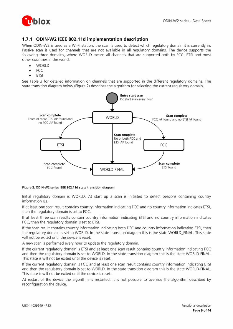
1.7.1 ODIN-W2 IEEE 802.11d implementation description When ODIN-W2 is used as a Wi-Fi station, the scan is used to detect which regulatory domain it is currently in. Passive scan is used for channels that are not available in all regulatory domains. The device supports the following three domains, where WORLD means all channels that are supported both by FCC, ETSI and most other countries in the world:
• WORLD • FCC • ETSI
See Table 3 for detailed information on channels that are supported in the different regulatory domains. The state transition diagram below (Figure 2) describes the algorithm for selecting the current regulatory domain.
Figure 2: ODIN-W2 series IEEE 802.11d state transition diagram
Initial regulatory domain is WORLD. At start up a scan is initiated to detect beacons containing country information IEs.
If at least one scan result contains country information indicating FCC and no country information indicates ETSI, then the regulatory domain is set to FCC.
If at least three scan results contain country information indicating ETSI and no country information indicates FCC, then the regulatory domain is set to ETSI.
If the scan result contains country information indicating both FCC and country information indicating ETSI, then the regulatory domain is set to WORLD. In the state transition diagram this is the state WORLD_FINAL. This state will not be exited until the device is reset.
A new scan is performed every hour to update the regulatory domain.
If the current regulatory domain is ETSI and at least one scan result contains country information indicating FCC and then the regulatory domain is set to WORLD. In the state transition diagram this is the state WORLD-FINAL. This state is will not be exited until the device is reset.
If the current regulatory domain is FCC and at least one scan result contains country information indicating ETSI and then the regulatory domain is set to WORLD. In the state transition diagram this is the state WORLD-FINAL. This state is will not be exited until the device is reset.
At restart of the device the algorithm is restarted. It is not possible to override the algorithm described by reconfiguration the device.
WORLD
FCC
WORLD-FINAL
ETSI
Scan complete FCC AP found and no ETSI AP found
Scan complete ETSI found
Scan complete Three or more ETSI AP found and
no FCC AP found
Scan complete FCC found
Scan complete No or both FCC and ETSI AP found
Entry start scan Do start scan every hour
ODIN-W2 series - Data Sheet
UBX-14039949 - R13 Functional description
Page 10 of 44
Regulatory Domain Band Tx Channels
WORLD 2.4 GHz 1, 2, 3, 4, 5, 6, 7, 8, 9, 10, 11
U-NII-1 36, 40, 44, 48
U-NII-2 52, 56, 60, 64
U-NII-2e 100, 104, 108, 112, 116, 132, 136, 140
U-NII-3 -
ETSI 2.4 GHz 1, 2, 3, 4, 5, 6, 7, 8, 9, 10, 11, 12, 13
U-NII-1 36, 40, 44, 48
U-NII-2 52, 56, 60, 64
U-NII-2e 100, 104, 108, 112, 116, 120, 124, 128, 132, 136, 140
U-NII-3 149, 153, 157, 161, 165
FCC 2.4 GHz 1, 2, 3, 4, 5, 6, 7, 8, 9, 10, 11
U-NII-1 36, 40, 44, 48
U-NII-2 52, 56, 60, 64
U-NII-2e 100, 104, 108, 112, 116, 132, 136, 140
U-NII-3 149, 153, 157, 161, 165
Table 3: Channel list for supported regulatory domains
The maximum output power is reduced on some channels depending on regulatory requirements. For example, frequency band edge requirements can limit the output power on channels close to band edges.
1.8 MAC addresses The ODIN-W2 module series has four unique consecutive MAC addresses reserved for each module, from which the three first addresses are stored in the configuration memory during production. The first Bluetooth MAC address is available in the Data Matrix on the label (see section 10.2). The last MAC address is not stored in the configuration memory but is reserved for usage with the module.
MAC address Assignment Last bits of MAC address Example
Module 1, address 1 Bluetooth 00 D4:CA:6E:90:04:90
Module 1, address 2 Wi-Fi 01 D4:CA:6E:90:04:91
Module 1, address 3 RMII/Ethernet 10 D4:CA:6E:90:04:92
Module 1, address 4 Reserved 11 D4:CA:6E:90:04:93
Module 2, address 1 Bluetooth 00 D4:CA:6E:90:04:94
Module 2, address 2 Wi-Fi 01 D4:CA:6E:90:04:95
Module 2, address 3 RMII/Ethernet 10 D4:CA:6E:90:04:96
Module 2, address 4 Reserved 11 D4:CA:6E:90:04:97
Table 4: Example MAC address assignment for two modules
ODIN-W2 series - Data Sheet
UBX-14039949 - R13 Interfaces
Page 11 of 44
2 Interfaces The ODIN-W2 series module is a surface mounted device (SMD). Due to the fact that ports of the ODIN-
W2 module is not tested against fast transients, RF common mode, transients and surge, the module is not allowed to be connected with cables longer than 3 m.
2.1 Power management
In order to fulfill the safety standard EN 60950-1, the unit must be supplied by a limited power source.
2.1.1 Module supply input (VCC) The ODIN-W2 series modules must be supplied through the VCC pin by a DC power supply. Voltage must be stable, because during operation the current drawn from VCC can vary significantly based on the power consumption profile of the Bluetooth/Wi-Fi technologies.
2.1.2 Digital I/O interfaces supply output (V_INT) The ODIN-W2 series modules provide a 1.8 V supply rail output on the V_INT pin, which is internally generated when the module is powered on. The same voltage domain is used internally to supply the generic digital interfaces of the modules. The V_INT supply output can be used instead of an external discrete regulator. See the Electrical specification section for maximum output current.
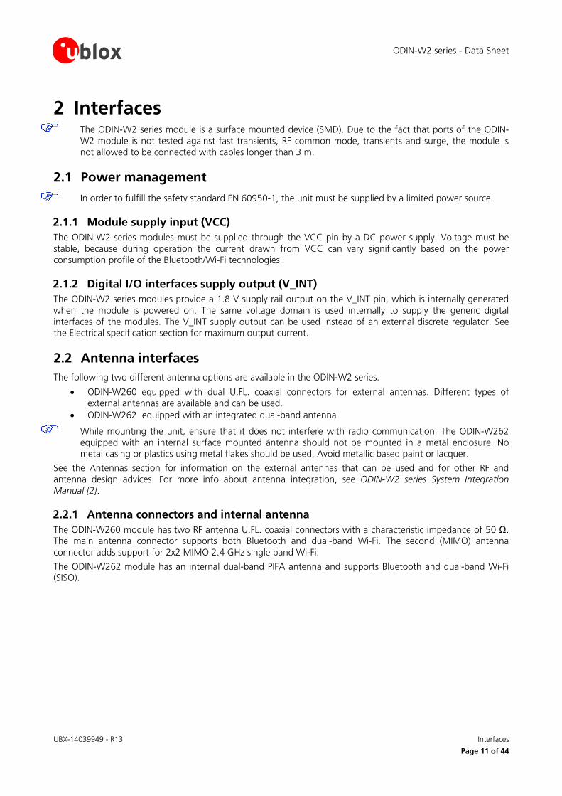
2.2 Antenna interfaces The following two different antenna options are available in the ODIN-W2 series:
• ODIN-W260 equipped with dual U.FL. coaxial connectors for external antennas. Different types of external antennas are available and can be used.
• ODIN-W262 equipped with an integrated dual-band antenna
While mounting the unit, ensure that it does not interfere with radio communication. The ODIN-W262 equipped with an internal surface mounted antenna should not be mounted in a metal enclosure. No metal casing or plastics using metal flakes should be used. Avoid metallic based paint or lacquer.
See the Antennas section for information on the external antennas that can be used and for other RF and antenna design advices. For more info about antenna integration, see ODIN-W2 series System Integration Manual [2].
2.2.1 Antenna connectors and internal antenna The ODIN-W260 module has two RF antenna U.FL. coaxial connectors with a characteristic impedance of 50 Ω. The main antenna connector supports both Bluetooth and dual-band Wi-Fi. The second (MIMO) antenna connector adds support for 2x2 MIMO 2.4 GHz single band Wi-Fi.
The ODIN-W262 module has an internal dual-band PIFA antenna and supports Bluetooth and dual-band Wi-Fi (SISO).
ODIN-W2 series - Data Sheet
UBX-14039949 - R13 Interfaces
Page 12 of 44
Figure 3: ODIN-W260 with connectors for external antennas and ODIN-W262 with an internal antenna
2.3 Data communication interfaces The ODIN-W2 series provides several data communication interfaces which are described below.
2.3.1 UART interface The ODIN-W2 series modules include a 6-wire UART for communication with an application host processor (AT commands, Data communication and software upgrades).
The following UART signals are available:
• Data lines (RXD as input, TXD as output) • Hardware flow control lines (CTS as input, RTS as output) • Link status (DTR as output, DSR as input)
It is recommended to use CMOS compatible signal levels. See u-blox Short Range AT Commands Manual [1] and ODIN-W2 series System Integration Manual [2] for more information about the UART interface.
2.3.2 Ethernet interface The ODIN-W2 series modules include an integrated Ethernet MAC to communicate with other networked nodes over a shared medium. It supports 10/100 Mbit/s communication and can operate in both full- and half-duplex (CSMA/CD).
The Ethernet interface includes:
• RMII either for MAC to PHY or Ethernet MAC to MAC communication. • SMI for PHY configuration
ODIN-W2 series - Data Sheet
UBX-14039949 - R13 Interfaces
Page 13 of 44
The IO voltage of the ODIN-W2 is 1.8 V, which means that the RMII interface operates outside the RMII specification v1.2. If the RMII is to be connected to a PHY circuit, then that circuit must support 1.8 V operation. If a direct RMII to RMII connection is used, then a level shifter might be needed depending on the selected host. The selected hardware setup must be verified on the application board to guarantee operation.
2.3.2.1 RMII
The RMII uses 7 signals in total. The interface requires an external 50 MHz clock source either from a compatible PHY chip or an external oscillator. The ODIN-W2 module cannot provide this clock signal by itself.
2.3.2.2 SMI (MDC/MDIO management interface)
The two-wire SMI is used to configure the PHY chips. It uses a clock line and a data line to clock data to and from the PHY chips registers.
ODIN-W2 series - Data Sheet
UBX-14039949 - R13 System functions
Page 14 of 44
3 System functions
3.1 Module power modes The ODIN-W2 series module does not have an internal low power oscillator (LPO) which is required for low power modes. An external 32.768 kHz LPO signal can be supplied externally via the LPO_CLK pin if low power modes are required.
3.2 Module reset The ODIN-W2 series modules can be reset (rebooted) in one of the following ways:
• Low level on the RESET_N pin, which is normally set high by an internal pull-up. This causes “hardware” reset of the module. The RESET_N line should be driven by an open drain, open collector or contact switch.
• Using a reset AT command (see the u-blox Short Range AT Commands Manual [1]). This causes “software” reset of the module.
3.3 System IO The module has the following six different configurable IOs that can be used to indicate different system states or to be used as inputs, thus setting the module in different states:
• SWITCH_0 • RED • GREEN/SWITCH_1 • BLUE • UART_DTR • UART_DSR
See the Pin definition section for more information on the separate IOs. For more information on the use and configuration of the System IOs, see the u-blox Short Range AT Commands Manual [1].
ODIN-W2 series - Data Sheet
UBX-14039949 - R13 Pin definition
Page 15 of 44
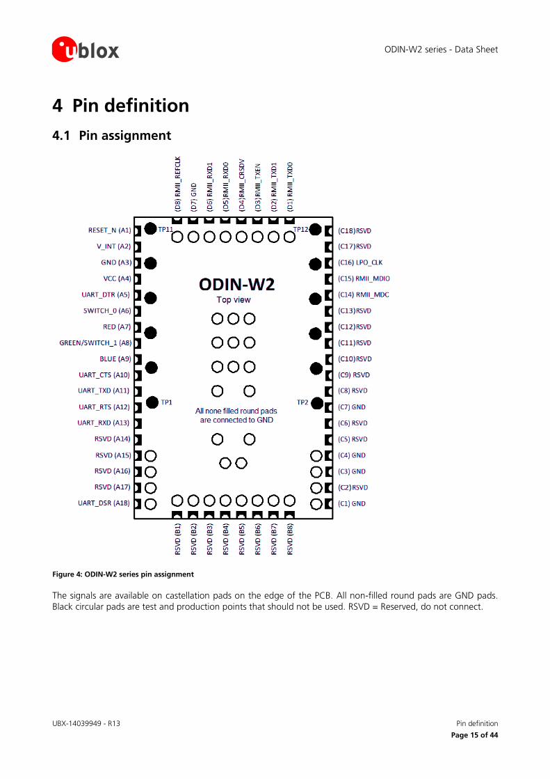
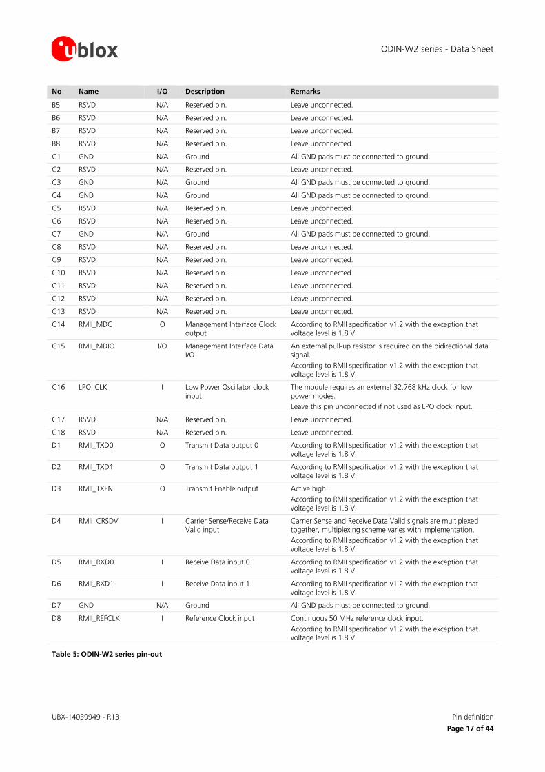
4 Pin definition
4.1 Pin assignment
Figure 4: ODIN-W2 series pin assignment
The signals are available on castellation pads on the edge of the PCB. All non-filled round pads are GND pads. Black circular pads are test and production points that should not be used. RSVD = Reserved, do not connect.
ODIN-W2 series - Data Sheet
UBX-14039949 - R13 Pin definition
Page 16 of 44
No Name I/O Description Remarks
A1 RESET_N I External reset input. Internal active pull-up to V_INT.
A2 V_INT O Regulated output of the internal I/O voltage.
1.8 V, maximum output current 100mA. The maximum output current can be limited by the internal current consumption of the V_INT rail. See the Power consumption section.
A3 GND N/A Ground All GND pads must be connected to ground.
A4 VCC I Module power supply. 3.0 - 3.6 V power supply.
A5 UART_DTR O UART Data Terminal Ready. Active low. Can also be used as a System IO. See the System IO section for more information. See the u-blox Short Range AT Commands Manual [1] for more information about the pin functionality.
A6 SWITCH_0 I Connect on external signal. Active low. A secondary function is that the module will restore all factory settings if both the SWITCH_1 and SWITCH_0 signals are low during start up. See the u-blox Short Range AT Commands Manual [1] for more information about the pin functionality.
A7 RED O Logic Red LED Signal. Active low. See the System IO section for more information. See the u-blox Short Range AT Commands Manual [1] for more information about the pin functionality.
A8 GREEN/ SWITCH_1
O/I This signal is multiplexed: GREEN: Logic Green LED Signal. SWITCH_1: Default Serial Settings.
Active low. The GREEN signal is not valid until 500ms after startup. See the System IO section for more information. If the level on this pin is pulled-down during start-up the unit goes back to default serial settings. The SWITCH_1 input is only active during the first 500ms after startup. The module will restore all factory settings if both the SWITCH_1 and SWITCH_0 signals are low during start up. See the u-blox Short Range AT Commands Manual [1] for more information about the pin functionality.
A9 BLUE O Logic Blue LED Signal. Active low. See the System IO section for more information. See the u-blox Short Range AT Commands Manual [1] for more information about the pin functionality.
A10 UART_CTS I UART Clear To Send, Hardware flow control.
Active low.
A11 UART_TXD O UART Transmit.
A12 UART_RTS O UART Request To Send, Hardware flow control.
Active low.
A13 UART_RXD I UART Receive.
A14 RSVD N/A Reserved pin. Leave unconnected.
A15 RSVD N/A Reserved pin. Leave unconnected.
A16 RSVD N/A Reserved pin. Leave unconnected.
A17 RSVD N/A Reserved pin. Leave unconnected.
A18 UART_DSR I UART Data Set Ready. Active low. Can also be used as a System IO. See the System IO section for more information. See the u-blox Short Range AT Commands Manual [1] for more information about the pin functionality.
B1 RSVD N/A Reserved pin. Leave unconnected.
B2 RSVD N/A Reserved pin. Leave unconnected.
B3 RSVD N/A Reserved pin. Leave unconnected.
B4 RSVD N/A Reserved pin. Leave unconnected.
ODIN-W2 series - Data Sheet
UBX-14039949 - R13 Pin definition
Page 17 of 44
No Name I/O Description Remarks
B5 RSVD N/A Reserved pin. Leave unconnected.
B6 RSVD N/A Reserved pin. Leave unconnected.
B7 RSVD N/A Reserved pin. Leave unconnected.
B8 RSVD N/A Reserved pin. Leave unconnected.
C1 GND N/A Ground All GND pads must be connected to ground.
C2 RSVD N/A Reserved pin. Leave unconnected.
C3 GND N/A Ground All GND pads must be connected to ground.
C4 GND N/A Ground All GND pads must be connected to ground.
C5 RSVD N/A Reserved pin. Leave unconnected.
C6 RSVD N/A Reserved pin. Leave unconnected.
C7 GND N/A Ground All GND pads must be connected to ground.
C8 RSVD N/A Reserved pin. Leave unconnected.
C9 RSVD N/A Reserved pin. Leave unconnected.
C10 RSVD N/A Reserved pin. Leave unconnected.
C11 RSVD N/A Reserved pin. Leave unconnected.
C12 RSVD N/A Reserved pin. Leave unconnected.
C13 RSVD N/A Reserved pin. Leave unconnected.
C14 RMII_MDC O Management Interface Clock output
According to RMII specification v1.2 with the exception that voltage level is 1.8 V.
C15 RMII_MDIO I/O Management Interface Data I/O
An external pull-up resistor is required on the bidirectional data signal. According to RMII specification v1.2 with the exception that voltage level is 1.8 V.
C16 LPO_CLK I Low Power Oscillator clock input
The module requires an external 32.768 kHz clock for low power modes. Leave this pin unconnected if not used as LPO clock input.
C17 RSVD N/A Reserved pin. Leave unconnected.
C18 RSVD N/A Reserved pin. Leave unconnected.
D1 RMII_TXD0 O Transmit Data output 0 According to RMII specification v1.2 with the exception that voltage level is 1.8 V.
D2 RMII_TXD1 O Transmit Data output 1 According to RMII specification v1.2 with the exception that voltage level is 1.8 V.
D3 RMII_TXEN O Transmit Enable output Active high. According to RMII specification v1.2 with the exception that voltage level is 1.8 V.
D4 RMII_CRSDV I Carrier Sense/Receive Data Valid input
Carrier Sense and Receive Data Valid signals are multiplexed together, multiplexing scheme varies with implementation. According to RMII specification v1.2 with the exception that voltage level is 1.8 V.
D5 RMII_RXD0 I Receive Data input 0 According to RMII specification v1.2 with the exception that voltage level is 1.8 V.
D6 RMII_RXD1 I Receive Data input 1 According to RMII specification v1.2 with the exception that voltage level is 1.8 V.
D7 GND N/A Ground All GND pads must be connected to ground.
D8 RMII_REFCLK I Reference Clock input Continuous 50 MHz reference clock input. According to RMII specification v1.2 with the exception that voltage level is 1.8 V.
Table 5: ODIN-W2 series pin-out
ODIN-W2 series - Data Sheet
UBX-14039949 - R13 Electrical specification
Page 18 of 44
5 Electrical specification Stressing the device above one or more of the ratings listed in the Absolute maximum ratings section may cause permanent damage. These are stress ratings only. Operating the module at these or at any conditions other than those specified in the Operating conditions section should be avoided. Exposure to absolute maximum rating conditions for extended periods may affect device reliability.
5.1 Absolute maximum ratings
Symbol Description Condition Min Maximum Unit
VCC Module supply voltage Input DC voltage at VCC pin -0.3 5.5* V
GDI Generic digital interfaces Input DC voltage at Generic digital interfaces pins
-0.3 2.2 V
ERS External reset signal Input DC voltage at RESET_N pin -0.3 5.2 V
Tstg Storage temperature -40 +85 ºC * 5.5 V up to 10 s cumulative in 7 years, 5 V cumulative to 250 s, 4.8 V cumulative to 2.33 years - all includes charging dips and peaks.
Table 6: Absolute maximum ratings
5.1.1 Maximum ESD Parameter Maximum Unit Remarks
ESD immunity for antenna connector shielding
6000 V Contact Discharge according to IEC 61000-4-2
8000 V Air Discharge according to IEC 61000-4-2
ESD sensitivity for all pins 1000 V Human Body Model according to ANSI/ESDA/JEDEC JS-001
250 V Charged Device Model according to EIA-JEDEC JESD22-C101E
Table 7: Maximum ESD ratings
5.2 Operating conditions
Operating condition ranges define those limits within which the functionality of the device is guaranteed.
5.2.1 Temperature range Parameter Min Maximum Unit
Storage temperature -40 +85 ºC
Operating temperature -40 +85 ºC
Table 8: Temperature range
5.2.2 Power supply Symbol Parameter Min Typ Maximum Unit
VCC Supply voltage 3.00 3.30 3.60 V
V_INT Output voltage 1.76 1.80 1.84 V
IVCC Supply voltage current drain1 - - 1.0 A
IV_INT Output voltage current drain - - 100 mA
Table 9: Power supply voltage
1 See Power consumption section for detailed information.
ODIN-W2 series - Data Sheet
UBX-14039949 - R13 Electrical specification
Page 19 of 44
5.2.3 I/O DC characteristics Symbol Parameter Min Typ Maximum Unit
VIL LOW level input voltage 0 0.5 V
VIH HIGH level input voltage 1.31 1.8 2.0 V
VOL LOW level output voltage 0 0.4 V
VOH HIGH level output voltage 1.34 1.8 V
IIO I/O pin sink and source current 4.0* mA
CIO I/O pin input capacitance 5 pF
RPU Internal active pull-up resistance All IO pins except for UART_RXD 30 40 50 kΩ
UART_RXD 8 11 15 kΩ
RPD Internal active pull-down resistance 30 40 50 kΩ * 8.0 mA is possible but the output voltage level is not guaranteed.
Table 10: I/O DC characteristics
5.2.4 Reset characteristics Symbol Parameter Conditions Min Typ Maximum Unit
VIL(RESET_N) RESET_N Input low level voltage 0.5 V
VIH(RESET_N) RESET_N Input high level voltage 1.3 V
Vhys(RESET_N) RESET_N Schmitt trigger voltage hysteresis
200 mV
RPU(RESET_N) Internal RESET_N pull-up resistance 8 kΩ
CRESET_N Internal RESET_N capacitance 100 nF
VF(RESET_N) RESET_N Input filtered pulse 100 ns
Table 11: Reset characteristics
5.2.5 LPO clock The ODIN-W2 series module does not have an internal low power oscillator (LPO) required for low power modes. An LPO can be supplied from an external oscillator if low power modes are required.
Symbol Parameter Min Typ Maximum Unit
LPO32.768kHz Input clock frequency 32.768 kHz
Input slow clock accuracy (Initial + temp + aging)
±150 ppm
Tr/Tf Input transition time Tr/Tf -10% to 90% 100 ns
Frequency input duty cycle 20 50 80 %
VIH Input voltage limits (Square wave, DC-coupled)
1.31 1.8 V
VIL 0 0.5 V
Input capacitance 10 pF
Table 12: External LPO clock characteristics
5.2.6 Universal asynchronous serial interface (UART) Symbol Parameter Min Typ Maximum Unit
fbaud Baud rate 2400 115200 5.25M bit/s
Table 13: UART characteristics
ODIN-W2 series - Data Sheet
UBX-14039949 - R13 Electrical specification
Page 20 of 44
5.3 Power consumption
5.3.1 General power consumption VCC = 3.3 V, TA = 25 °C unless otherwise specified.
Symbol Parameter Conditions Average Peak Unit
IDD Supply current Reset 5.2 6.0 mA Startup 130 800* mA Idle, not connected, default configuration 30 65 mA Idle, not connected, no running services** 30 60 mA Stop mode*** TBD TBD mA
IDD_MAXIMUM Absolute maximum current drain - 1.0 A * Wi-Fi and Bluetooth calibration during the startup phase causes large short current peaks. ** No server running and Bluetooth Connectable and Discoverable turned off. *** Feature not supported in the current software version. See u-blox Short Range AT Commands manual [1] for more information.
Table 14: General current consumption
5.3.2 Wi-Fi 2.4 GHz power consumption VCC = 3.3 V, TA = 25 °C unless otherwise specified.
Symbol Parameter Conditions Average Peak Unit
IDDW24 Supply current not connected
Scan, 11 channels, 300 ms 100 450 mA Idle, Connected DTIM = 1, Tbeacon = 100 ms 36 100 mA Idle, Connected DTIM = 5, Tbeacon = 100 ms 32 100 mA
IDDW24_TX Supply current transmitting
802.11b 110 460 mA
802.11g 110 450 mA
IDDW24_RX Supply current receiving
802.11b 110 460 mA
802.11g 110 460 mA
Table 15: Current consumption for Wi-Fi 2.4 GHz
5.3.3 Wi-Fi 5 GHz power consumption VCC = 3.3 V, Tamb = 25 °C
Symbol Parameter Conditions Average Peak Unit
IDDW5 Supply current not connected Scan, 4 channels, 100 ms 100 510 mA Idle, Connected DTIM = 1, Tbeacon = 100 ms 36 100 mA Idle, Connected DTIM = 5****, Tbeacon = 100 ms 32 100 mA
IDDW5_TX Supply current transmitting 802.11a 250 650 mA
IDDW5_RX Supply current receiving 802.11a 102 610 mA
Table 16: Current consumption for Wi-Fi 5 GHz
5.3.4 Classic Bluetooth power consumption VCC = 3.3 V, Tamb = 25 °C
Symbol Parameter Conditions Average Peak Unit
IDDBT_NDNC Supply current not connected
Not discoverable, Not connectable 30 65 mA
IDDBT_NDC Not discoverable, Connectable, scan interval = TBD, scan window = TBD
30 65 mA
IDDBT_DC Discoverable, Connectable, scan interval = TBD, scan window = TBD
30 65 mA
IDDBT_INQ Supply current inquiry 47 120 mA
IDDBT_IDLE Supply current connected Idle 32 120 mA
IDDBT_TX1Mb Transmitting 56 120 mA
IDDBT_RX1Mb Receiving 46 120 mA
Table 17: Current consumption for classic Bluetooth
ODIN-W2 series - Data Sheet
UBX-14039949 - R13 Electrical specification
Page 21 of 44
5.3.5 Bluetooth Low Energy (BLE) power consumption VCC = 3.3 V, Tamb = 25 °C
Symbol Parameter Conditions Average Peak Unit
IDDBLE_CD_NC Supply current not connected
Central device Idle 29 65 mA
IDDBLE_CD_INQ Low Energy Inquiry 48 80 mA
IDDBLE_PD_NC Peripheral device
Idle 29 65 mA
IDDBLE_PD_ADV Advertising 29 65 mA
IDDBLE_CD_IDLE Supply current connected
Central device Idle 44 100 mA
IDDBLE_CD_TX Transmitting 45 100 mA
IDDBLE_CD_RX Receiving 45 100 mA
IDDBLE_PD_IDLE Peripheral device
Idle 29 100 mA
IDDBLE_PD_TX Transmitting 30 100 mA
IDDBLE_PD_RX Receiving 30 100 mA
Table 18: Current consumption for Bluetooth Low Energy (BLE)
5.4 RF characteristics
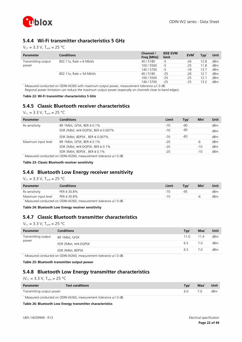
5.4.1 Wi-Fi receiver characteristics 2.4 GHz VCC = 3.3 V, Tamb = 25 °C
Parameter Conditions Antenna port Channel / Freq [MHz]
IEEE limit
Typ* Unit
Receive sensitivity 802.11b, Rate = 1 Mbit/s, PER ≤ 8% MAIN port 6 / 2437 -76 -95 dBm 802.11b, Rate = 11 Mbit/s, PER ≤ 8% MAIN port 6 / 2437 -76 -86 dBm 802.11g, Rate = 6 Mbit/s, PER ≤ 10% MAIN port 6 / 2437 -82 -90 dBm 802.11g, Rate = 54 Mbit/s, PER ≤ 10% MAIN port 6 / 2437 -65 -72 dBm
* Measured conducted on ODIN-W260, measurement tolerance ±1.0 dB.
Table 19: Receiver characteristics for 2.4 GHz Wi-Fi
5.4.2 Wi-Fi receiver characteristics 5 GHz VCC = 3.3 V, Tamb = 25 °C
Parameter Conditions Channel / Freq [MHz]
IEEE limit
Typ* Unit
Receive sensitivity 802.11a, Rate = 6 Mbit/s, PER ≤ 10% 36 / 5180 -82 -90 dBm 100 / 5500 -82 -90 dBm 140 / 5825 -82 -90 dBm
802.11a, Rate = 48 Mbit/s, PER ≤ 10% 36 / 5180 -66 -72 dBm 100 / 5500 -66 -72 dBm 140 / 5825 -66 -72 dBm
* Measured conducted on ODIN-W260, measurement tolerance ±1.0 dB.
Table 20: Receiver characteristics for 5 GHz Wi-Fi
5.4.3 Wi-Fi transmitter characteristics 2.4 GHz VCC = 3.3 V, Tamb = 25 °C
Parameter Conditions Antenna port IEEE EVM limit
EVM* Typ* Unit
Transmitting output power
802.11b, Rate = 1 Mbit/s MAIN port -14 -28 11.2 dBm 802.11b, Rate = 11 Mbit/s MAIN port -14 -26 11.3 dBm 802.11g, Rate = 6 Mbit/s MAIN port -5 -21 14.2 dBm 802.11g, Rate = 54 Mbit/s MAIN port -25 -29 12.1 dBm
* Measured conducted on ODIN-W260 with maximum output power, measurement tolerance ±1.0 dB. Regional power limitation can reduce the maximum output power (especially on channels close to band edges).
Table 21: Wi-Fi transmitter characteristics 2.4 GHz
ODIN-W2 series - Data Sheet
UBX-14039949 - R13 Electrical specification
Page 22 of 44
5.4.4 Wi-Fi transmitter characteristics 5 GHz VCC = 3.3 V, Tamb = 25 °C
Parameter Conditions Channel / Freq [MHz]
IEEE EVM limit
EVM* Typ* Unit
Transmitting output power
802.11a, Rate = 6 Mbit/s 40 / 5180 -5 -26 12.8 dBm 100 / 5500 -5 -25 11.8 dBm 140 / 5700 -5 -18 13.7 dBm
802.11a, Rate = 54 Mbit/s 40 / 5180 -25 -26 12.7 dBm 100 / 5500 -25 -25 12.1 dBm 140 / 5700 -25 -25 13.2 dBm
* Measured conducted on ODIN-W260 with maximum output power, measurement tolerance ±1.0 dB. Regional power limitation can reduce the maximum output power (especially on channels close to band edges).
Table 22: Wi-Fi transmitter characteristics 5 GHz
5.4.5 Classic Bluetooth receiver characteristics VCC = 3.3 V, Tamb = 25 °C
Parameter Conditions Limit Typ* Min* Unit
Rx sensitivity BR 1Mbit, GFSK, BER ≤ 0.1% -70 -90 dBm
EDR 2Mbit, π/4-DQPSK, BER ≤ 0.007% -70 -90 dBm
EDR 3Mbit, 8DPSK , BER ≤ 0.007% -70 -83 dBm
Maximum input level BR 1Mbit, GFSK, BER ≤ 0.1% -20 -6 dBm
EDR 2Mbit, π/4-DQPSK, BER ≤ 0.1% -20 -10 dBm
EDR 3Mbit, 8DPSK , BER ≤ 0.1% -20 -10 dBm * Measured conducted on ODIN-W260, measurement tolerance ±1.0 dB.
Table 23: Classic Bluetooth receiver sensitivity
5.4.6 Bluetooth Low Energy receiver sensitivity VCC = 3.3 V, Tamb = 25 °C
Parameter Conditions Limit Typ* Min* Unit
Rx sensitivity PER ≤ 30.8% -70 -95 dBm
Maximum input level PER ≤ 30.8% -10 -6 dBm * Measured conducted on ODIN-W260, measurement tolerance ±1.0 dB.
Table 24: Bluetooth Low Energy receiver sensitivity
5.4.7 Classic Bluetooth transmitter characteristics VCC = 3.3 V, Tamb = 25 °C
Parameter Conditions Typ* Max* Unit
Transmitting output power
BR 1Mbit, GFSK 11.0 11.4 dBm
EDR 2Mbit, π/4-DQPSK 6.5 7.0 dBm
EDR 3Mbit, 8DPSK 6.5 7.0 dBm * Measured conducted on ODIN-W260, measurement tolerance ±1.0 dB.
Table 25: Bluetooth transmitter output power
5.4.8 Bluetooth Low Energy transmitter characteristics (VCC = 3.3 V, Tamb = 25 °C
Parameter Test conditions Typ* Max* Unit
Transmitting output power 6.0 7.0 dBm * Measured conducted on ODIN-W260, measurement tolerance ±1.0 dB.
Table 26: Bluetooth Low Energy transmitter characteristics
ODIN-W2 series - Data Sheet
UBX-14039949 - R13 Mechanical specifications
Page 23 of 44
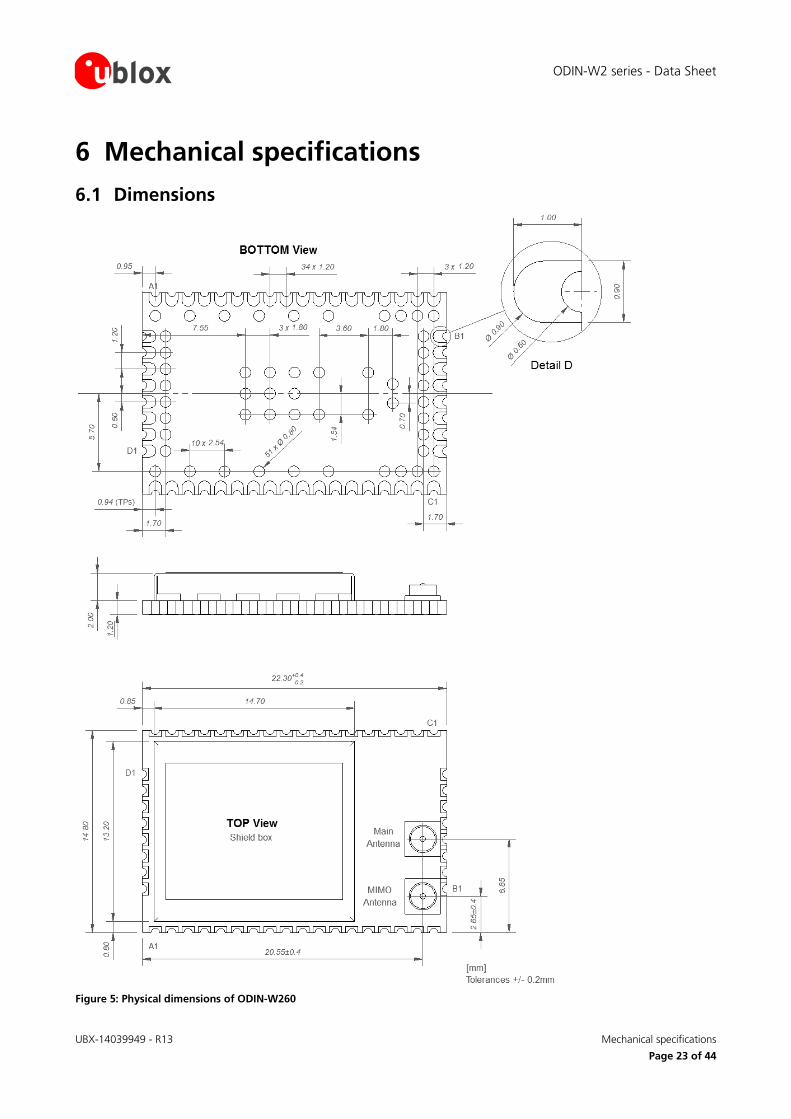
6 Mechanical specifications
6.1 Dimensions
Figure 5: Physical dimensions of ODIN-W260
ODIN-W2 series - Data Sheet
UBX-14039949 - R13 Mechanical specifications
Page 24 of 44
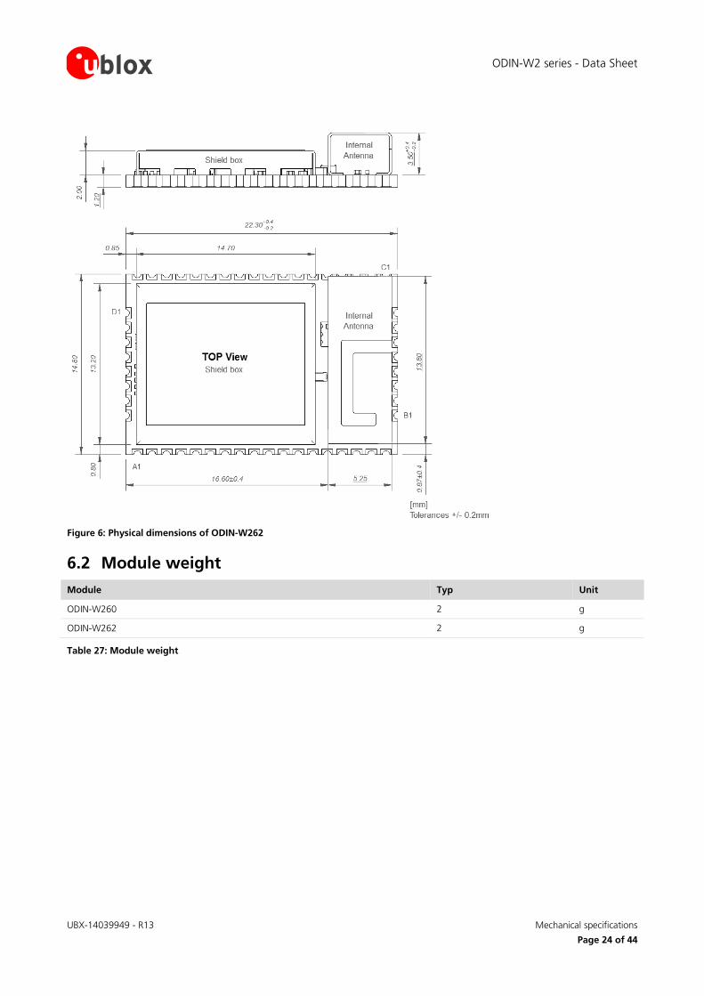
Figure 6: Physical dimensions of ODIN-W262
6.2 Module weight Module Typ Unit
ODIN-W260 2 g
ODIN-W262 2 g
Table 27: Module weight

ODIN-W2 series - Data Sheet
UBX-14039949 - R13 Qualification and approvals
Page 25 of 44
7 Qualification and approvals
7.1 Compliance with RoHS directive
The ODIN-W2 series modules comply with the "Directive 2011/65/EU of the European Parliament and the Council on the Restriction of Use of certain Hazardous Substances in Electrical and Electronic Equipment" (RoHS).
No natural rubbers, hygroscopic materials, or materials containing asbestos are employed.
7.2 European Union regulatory compliance Information about regulatory compliance of the European Union for ODIN-W2 series modules is available in the ODIN-W2 Declaration of Conformity [4].
7.3 Safety compliance
In order to fulfill the safety standard EN 60950-1, the unit must be supplied by a limited power source.
7.4 FCC and IC Compliance
7.4.1 IC compliance This device complies with Industry Canada license-exempt RSS standard(s).
Operation is subject to the following two conditions:
1. this device may not cause interference, and 2. this device must accept any interference, including interference that may cause undesired operation of
the device.
Under Industry Canada regulations, this radio transmitter may only operate using an antenna of a type and maximum (or lesser) gain approved for the transmitter by Industry Canada. To reduce potential radio interference to other users, the antenna type and its gain should be so chosen that the equivalent isotropically radiated power (e.i.r.p.) is not more than that necessary for successful communication.
The device for operation in the band 5150-5250 MHz is only for indoor use to reduce the potential for harmful interference to co-channel mobile satellite systems;
The maximum antenna gain permitted for devices in the bands 5250-5350 MHz and 5470-5725 MHz shall comply with the e.i.r.p. limit; and
The maximum antenna gain permitted for devices in the band 5725-5825 MHz shall comply with the e.i.r.p. limits specified for point-to-point and non point-to-point operation as appropriate.
Operation in the 5600-5650 MHz band is not allowed in Canada. High-power radars are allocated as primary users (i.e. priority users) of the bands 5250-5350 MHz and 5650-5850 MHz and that these radars could cause interference and/or damage to LE-LAN devices.
This equipment complies with IC RSS-102 radiation exposure limits set forth for an uncontrolled environment. This equipment should be installed and operated with minimum distance 20 cm between the radiator & your body.
7.4.2 Conformité aux normes d’IC Cet appareil est conforme à la(aux) norme(s) RSS sans licence d’Industry Canada.
Son utilisation est soumise aux deux conditions suivantes :
1. Cet appareil ne doit pas causer d’interférences et
ODIN-W2 series - Data Sheet
UBX-14039949 - R13 Qualification and approvals
Page 26 of 44
2. il doit accepter toutes interférences reçues, y compris celles susceptibles d’avoir des effets indésirables sur son fonctionnement.
Conformément aux réglementations d’Industry Canada, cet émetteur radio ne peut fonctionner qu’à l’aide d’une antenne dont le type et le gain maximal (ou minimal) ont été approuvés pour cet émetteur par Industry Canada. Pour réduire le risque d’interférences avec d’autres utilisateurs, il faut choisir le type d’antenne et son gain de telle sorte que la puissance isotrope rayonnée équivalente (p.i.r.e) ne soit pas supérieure à celle requise pour obtenir une communication satisfaisante.
Le dispositif de fonctionnement dans la bande 5150-5250 MHz est réservé à une utilisation en intérieur pour réduire le risqué d'interférences nuisibles à la co-canal systèmes mobiles par satellite.
Le gain d'antenne maximal autorisé pour les appareils dans les bandes 5250-5350 MHz et 5470-5725 MHz doit se conformer à la pire limite, et
le gain d'antenne maximal autorisé pour les appareils dans la bande 5725-5825 MHz doivent être conformes avec le pire limites spécifiées à point-à-ponctuelles et non point-à-point de fonctionnement selon qu'il convient.
Opération dans la bande 5600-5650 MHz n'est pas autorisée au Canada. Haute puissance radars sont désignés comme utilisateurs principaux (c.-àutilisateurs prioritaires) des bandes 5250-5350 MHz et 5650-5850 MHz et que ces radars pourraient causer des interférences et / ou des dommages à dispositifs LAN-EL.
Cet équipement respecte les limites d’exposition aux rayonnements IC RSS-102 définies pour un environnement non contrôlé. Il doit être installé et utilisé en maintenant une distance minimum de 20 cm entre le radiateur et votre corps.
7.4.3 FCC statement This device complies with Part 15 of the FCC Rules. Operation is subject to the following two conditions:
1. this device may not cause harmful interference, and 2. this device must accept any interference received, including interference that may cause undesired
operation.
This equipment has been tested and found to comply with the limits for a Class B digital device, pursuant to Part 15 of the FCC Rules. These limits are designed to provide reasonable protection against harmful interference in a residential installation. This equipment generates, uses and can radiate radio frequency energy and, if not installed and used in accordance with the instructions, may cause harmful interference to radio communications. However, there is no guarantee that interference will not occur in a particular installation. If this equipment does cause harmful interference to radio or television reception, which can be determined by turning the equipment off and on, the user is encouraged to try to correct the interference by one or more of the following measures:
• Reorient or relocate the receiving antenna. • Increase the separation between the equipment and receiver. • Connect the equipment into an outlet on a circuit different from that to which the receiver is
connected.
Consult the dealer or an experienced radio/TV technician for help.
The ODIN-W2 module is for OEM integrations only. The end-user product will be professionally installed in such a manner that only the authorized antennas are used.
Any changes or modifications NOT explicitly APPROVED by u-blox could cause the module to cease to comply with FCC rules part 15, and thus void the user's authority to operate the equipment.
ODIN-W2 series - Data Sheet
UBX-14039949 - R13 Qualification and approvals
Page 27 of 44
7.4.3.1 Cautions
Any changes or modification could cause the module to cease to comply with FCC rules part 15 and thus void the user's authority to operate the equipment.
§15.407 statement; in case of absence of information to transmit or operational failure the module types ODIN-W2 will automatically discontinue transmission.
7.4.4 Labeling requirements for end product For an end product using the ODIN-W2 modules there must be a label containing, at least, the following information:
This device contains
FCC ID: PVH0965
IC: 5325A-0965
The label must be affixed on an exterior surface of the end product such that it will be visible upon inspection in compliance with the modular approval guidelines developed by the FCC.
In accordance with 47 CFR § 15.19 the end product shall bear the following statement in a conspicuous location on the device:
"This device complies with Part 15 of the FCC Rules.
Operation is subject to the following two conditions;
(1) this device may not cause harmful interference, and
(2) this device must accept any interference received, including interference that may cause undesired operation."
When the device is so small or for such use that it is not practicable to place the statement above on it, the information shall be placed in a prominent location in the instruction manual or pamphlet supplied to the user or, alternatively, shall be placed on the container in which the device is marketed.
In case, where the final product will be installed in locations where the end-user is not able to see the FCC ID and/or this statement, the FCC ID and the statement shall also be included in the end-product manual.
7.4.4.1 IC requirement
If the end product using the ODIN-W2 module is able to operate in the band 5150-5250 MHz within Canada (IC) it is only allowed to be used indoor to reduce the potential for harmful interference to co-channel mobile satellite systems. The label of the end product MUST in this case be marked with the text “For indoor use only”:
This device contains
FCC ID: PVH0965
IC: 5325A-0965
For indoor use only
When the device is so small or for such use that it is not practicable to place the statement above on it, the information shall be placed in a prominent location in the instruction manual or pamphlet supplied to the user or, alternatively, shall be placed on the container in which the device is marketed. However, the FCC ID label including the “For indoor use only” text must be displayed on the device.
ODIN-W2 series - Data Sheet
UBX-14039949 - R13 Qualification and approvals
Page 28 of 44
7.5 Japan radio equipment compliance The ODIN-W2 module complies with the Japanese Technical Regulation Conformity Certification of Specified Radio Equipment (ordinance of MPT N°. 37, 1981), Article 2, Paragraph 1:
• Item 19 "2.4 GHz band wide band low power data communication system" • Item 19-3 “Low power data communications system in the 5.2/5.3 GHz band” • Item 19-3-2 “Low power data communications system in the 5.6 GHz band”
The ODIN-W2 module is restricted on the Japanese market to be used indoors only if the product is operating in the 5.2/5.3 GHz band. The information: “Indoor use only” translated into Japanese (この製品は屋内においての
み使用可能です) must be visible:
• on the certified end product. • on the product package in which the end product is marketed. • in the users / installation manual of the end product.
The indoor usage information is recommended to be printed close to the Giteki mark but it is also permitted to place that information on another prominent position.
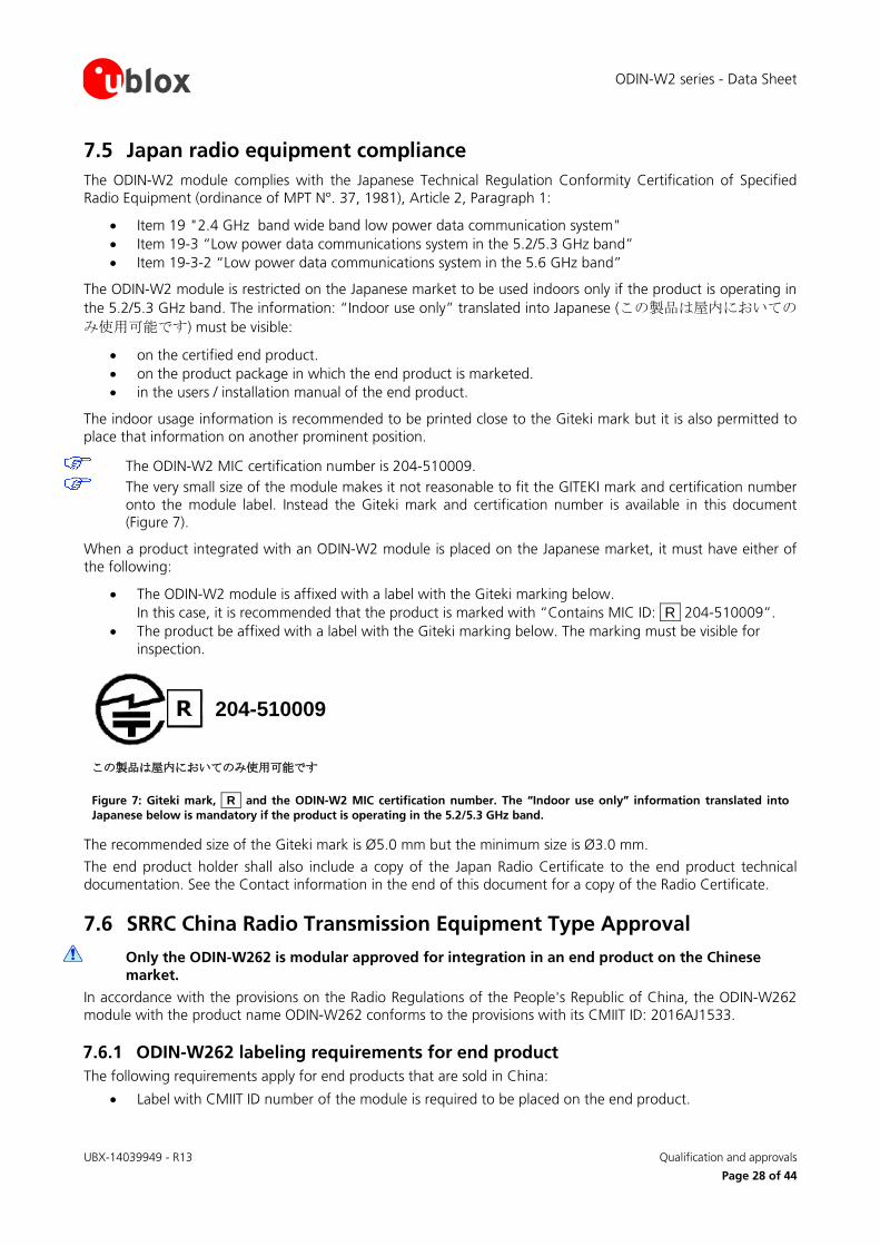
The ODIN-W2 MIC certification number is 204-510009. The very small size of the module makes it not reasonable to fit the GITEKI mark and certification number
onto the module label. Instead the Giteki mark and certification number is available in this document (Figure 7).
When a product integrated with an ODIN-W2 module is placed on the Japanese market, it must have either of the following:
• The ODIN-W2 module is affixed with a label with the Giteki marking below. In this case, it is recommended that the product is marked with “Contains MIC ID: R 204-510009”.
• The product be affixed with a label with the Giteki marking below. The marking must be visible for inspection.
204-510009
この製品は屋内においてのみ使用可能です
Figure 7: Giteki mark, R and the ODIN-W2 MIC certification number. The “Indoor use only” information translated into Japanese below is mandatory if the product is operating in the 5.2/5.3 GHz band.
The recommended size of the Giteki mark is Ø5.0 mm but the minimum size is Ø3.0 mm.
The end product holder shall also include a copy of the Japan Radio Certificate to the end product technical documentation. See the Contact information in the end of this document for a copy of the Radio Certificate.
7.6 SRRC China Radio Transmission Equipment Type Approval
Only the ODIN-W262 is modular approved for integration in an end product on the Chinese market.
In accordance with the provisions on the Radio Regulations of the People's Republic of China, the ODIN-W262 module with the product name ODIN-W262 conforms to the provisions with its CMIIT ID: 2016AJ1533.
7.6.1 ODIN-W262 labeling requirements for end product The following requirements apply for end products that are sold in China:
• Label with CMIIT ID number of the module is required to be placed on the end product.
ODIN-W2 series - Data Sheet
UBX-14039949 - R13 Qualification and approvals
Page 29 of 44
• The following statement must be included in Chinese in the Chinese user manual:
CMIIT ID: 2016AJ1533 (This device contains certified RF module which certificate number is CMIIT ID: 2016AJ1533)
7.7 NCC Taiwan compliance
7.7.1 Taiwan NCC Warning Statement
• 經型式認證合格之低功率射頻電機,非經許可,公司、商號或使用者均不得擅自變更頻率、 加大功率
或變更原設計之特性及功能。 • 低功率射頻電機之使用不得影響飛航安全及干擾合法通信;經發現有干擾現象時,應立即停用,並改
善至無干擾時方得繼續使用。前項合法通信,指依電信法規定作業之無線電通信。低功率射頻電機須
忍受合法通信或工業、科學及醫療用電波輻射性電機設備之干擾。
Statement translation:
• Without permission granted by the NCC, any company, enterprise, or user is not allowed to change frequency, enhance transmitting power or alter original characteristic as well as performance to an approved low power radio-frequency devices.
• The low power radio-frequency devices shall not influence aircraft security and interfere legal communications; If found, the user shall cease operating immediately until no interference is achieved. The said legal communications means radio communications is operated in compliance with the Telecommunications Act. The low power radio-frequency devices must be susceptible with the interference from legal communications or ISM radio wave radiated devices.
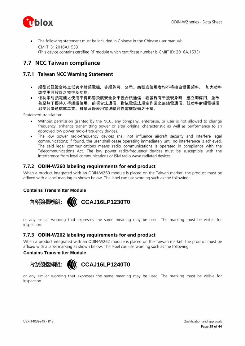
7.7.2 ODIN-W260 labeling requirements for end product When a product integrated with an ODIN-W260 module is placed on the Taiwan market, the product must be affixed with a label marking as shown below. The label can use wording such as the following:
Contains Transmitter Module
內含發射器模組:: CCAJ16LP1230T0
or any similar wording that expresses the same meaning may be used. The marking must be visible for inspection.
7.7.3 ODIN-W262 labeling requirements for end product When a product integrated with an ODIN-W262 module is placed on the Taiwan market, the product must be affixed with a label marking as shown below. The label can use wording such as the following:
Contains Transmitter Module
內含發射器模組:: CCAJ16LP1240T0
or any similar wording that expresses the same meaning may be used. The marking must be visible for inspection.
ODIN-W2 series - Data Sheet
UBX-14039949 - R13 Qualification and approvals
Page 30 of 44
7.8 Korean KCC certification
The ODIN-W2 series modules are certified by the Korea Communications Commission (KCC).
The KCC IDs for ODIN-W260 and ODIN-W262 are provided below:
• ODIN-W260 module: MSIP-CRM-ULX-ODIN-W260 • ODIN-W262 module: MSIP-CRM-ULX-ODIN-W262
7.9 Brazil compliance When a product containing ODIN-W2 module is placed on the Brazilian market, the product must be affixed with a label or marking containing the Anatel logo, ODIN-W2 Homologation number: 03883-16-05903 and a statement claiming that the device may not cause harmful interference but must accept it (Resolution No 506).
Statement translation:
“This equipment operates on a secondary basis and, consequently, must accept harmful interference, including from stations of the same kind, and may not cause harmful interference to systems operating on a primary basis.”
When the device is so small or for such use that it is not practicable to place the statement above on it, the information shall be placed in a prominent location in the instruction manual or pamphlet supplied to the user or, alternatively, shall be placed on the container in which the device is marketed.
In case, where the final product will be installed in locations where the end user is unable to see the Anatel logo, ODIN-W2 Homologation number and/or this statement, the Anatel logo, ODIN-W2 Homologation number, and the statement shall also be included in the end product manual.
7.10 Australia and New Zealand regulatory compliance The ODIN-W260 and ODIN-W262 modules are compliant with the standards made by the Australian Communications and Media Authority (ACMA).
The modules are compliant with AS/NZS 4268:2012 standard – Radio equipment and systems – Short range devices – Limits and methods of standard measurement. The ODIN-W2 module test reports can be used as part of the product certification and compliance folder. For more information on the test reports, send an email to the respective support team mail address as mentioned in the Contact section based on your location.
To meet overall Australian and/or New Zealand end product compliance, the integrator must create a compliance folder containing all the relevant compliance test reports such as RF, EMC, electrical safety and DoC (Declaration of Conformity) and so on. It is the responsibility of the integrator to know what is required in the compliance folder for ACMA compliance.
03883-16-05903
“Este equipamento opera em caráter secundário, isto é, não tem direito a proteção contra interferência prejudicial, mesmo de estações do mesmo tipo, e não pode causar interferência a sistemas operando em caráter primário.”
ODIN-W2 series - Data Sheet
UBX-14039949 - R13 Qualification and approvals
Page 31 of 44
For more information on Australia compliance, refer to the Australian Communications and Media Authority web site http://www.acma.gov.au/.
For more information on New Zealand compliance, refer to the New Zealand Radio Spectrum Management Group web site www.rsm.govt.nz.
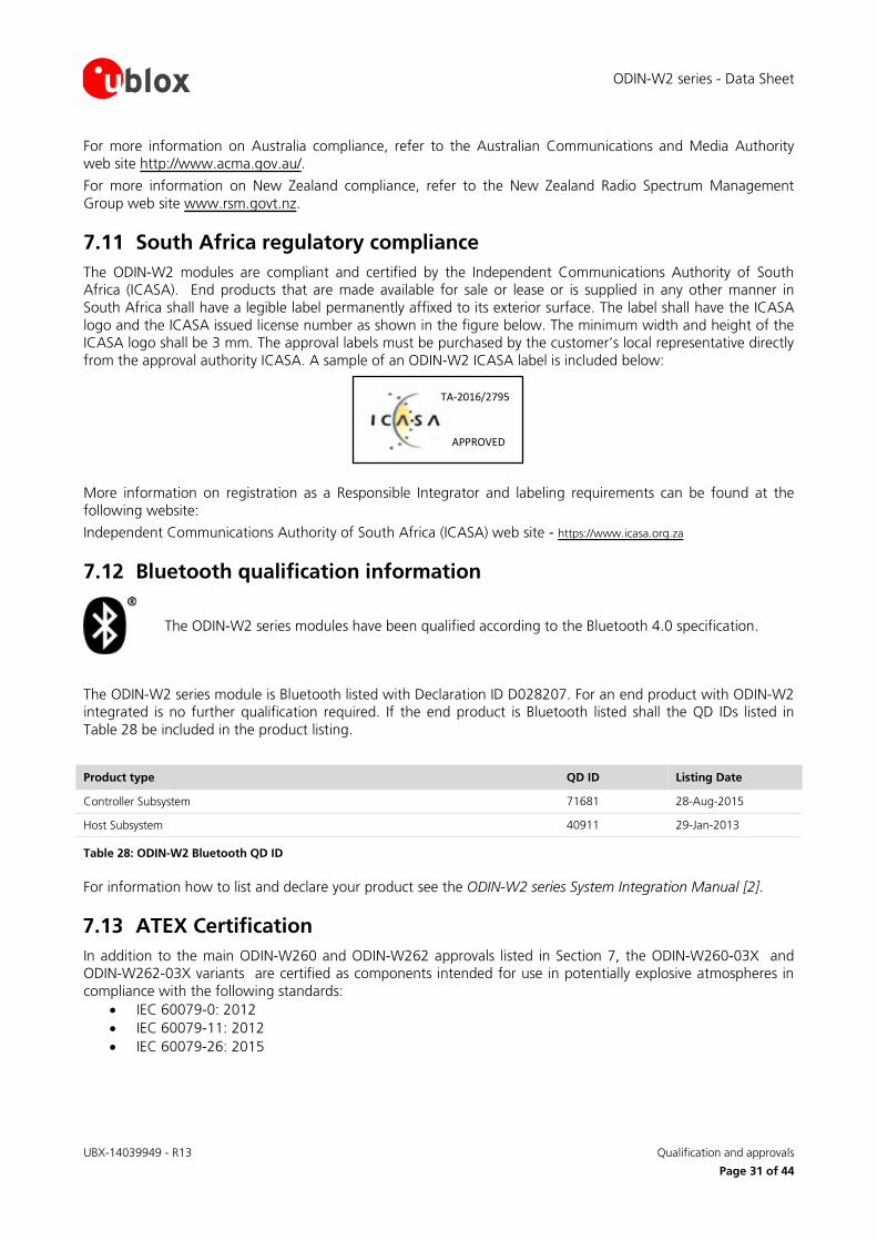
7.11 South Africa regulatory compliance The ODIN-W2 modules are compliant and certified by the Independent Communications Authority of South Africa (ICASA). End products that are made available for sale or lease or is supplied in any other manner in South Africa shall have a legible label permanently affixed to its exterior surface. The label shall have the ICASA logo and the ICASA issued license number as shown in the figure below. The minimum width and height of the ICASA logo shall be 3 mm. The approval labels must be purchased by the customer’s local representative directly from the approval authority ICASA. A sample of an ODIN-W2 ICASA label is included below:
More information on registration as a Responsible Integrator and labeling requirements can be found at the following website:
Independent Communications Authority of South Africa (ICASA) web site - https://www.icasa.org.za
7.12 Bluetooth qualification information
The ODIN-W2 series modules have been qualified according to the Bluetooth 4.0 specification.
The ODIN-W2 series module is Bluetooth listed with Declaration ID D028207. For an end product with ODIN-W2 integrated is no further qualification required. If the end product is Bluetooth listed shall the QD IDs listed in Table 28 be included in the product listing.
Product type QD ID Listing Date
Controller Subsystem 71681 28-Aug-2015
Host Subsystem 40911 29-Jan-2013
Table 28: ODIN-W2 Bluetooth QD ID
For information how to list and declare your product see the ODIN-W2 series System Integration Manual [2].
7.13 ATEX Certification In addition to the main ODIN-W260 and ODIN-W262 approvals listed in Section 7, the ODIN-W260-03X and ODIN-W262-03X variants are certified as components intended for use in potentially explosive atmospheres in compliance with the following standards:
• IEC 60079-0: 2012 • IEC 60079-11: 2012 • IEC 60079-26: 2015
APPROVED
TA-2016/2795
ODIN-W2 series - Data Sheet
UBX-14039949 - R13 Qualification and approvals
Page 32 of 44
The certification number of the ODIN-W2 ATEX certified variants according to the ATEX directive 2014/34/EU is: • SIQ 17 ATEX 002 U
The certification number of the ODIN-W26 ATEX certified variants according to the IECEx conformity assessment system is:
• IECEx SIQ 17.0002U According to the three standards listed above, the ODIN-W260-03X and ODIN-W262-03X modules are certified with the following marking:
• Ex II 1G, Ex ia IIC The above marking indicates that the ODIN-W260-03X and ODIN-W262-03X modules are certified as electrical equipments of:
• group ‘II’: intended for use in areas with explosive gas atmosphere other than mines susceptible to firedamp.
• category ‘1G’: intended for use in zone 0 hazardous areas, in which explosive atmospheres caused by mixtures of air and gases, vapors or mists are present continuously, for a long period or frequently.
• level of protection ‘ia’: intrinsically safe apparatus with very high level of protection, not capable of causing ignition in normal operation and with the application of one countable fault or a combination of any two countable fault plus those non-countable faults, which give the most onerous condition.
• subdivision ‘IIC’: intended for use in areas where the nature of the explosive gas atmosphere is considered very dangerous based on the Maximum Experimental Safe Gap or the Minimum Ignition Current ratio of the explosive gas atmosphere in which the equipment may be installed (a typical gas is hydrogen), so that the modules are also suitable for applications intended for use in subdivision IIB (typical gas is ethylene) and subdivision IIA (a typical gas is propane). Gas group IIC is the most stringent group and covers also groups IIB and IIA.
Section 5.2.1 defines the temperature range while using the ODIN-W260-03X and ODIN-W262-03X modules.
The RF radiating profile of the ODIN-W260-03X and ODIN-W262-03X modules is compliant with all the applicable ETSI standards. The maximum conducted and radiated output power for supported wireless technologies is stated in Table 2.
Section 10 describes the labelling of the ODIN-W260-03X and ODIN-W262-03X modules.
The following maximum input and equivalent parameters must be considered in the sub-division IIC:
• Ui = 3.6 V • Ii = 1.0 A • Ci = 111.6 μF • Li = 6.2 μH
ODIN-W2 series - Data Sheet
UBX-14039949 - R13 Antennas
Page 33 of 44
8 Antennas This chapter gives an overview of the different external antennas that can be fitted to the ODIN-W2 module.
This radio transmitter IC: 5325A-0965 has been approved by Industry Canada to operate with the antenna types listed below with the maximum permissible gain and required antenna impedance for each antenna type indicated. Antenna types not included in this list, having a gain greater than the maximum gain indicated for that type, are strictly prohibited for use with this device.
Cet émetteur radio IC: 5325A-0965 été approuvé par Industry Canada pour fonctionner avec les types d’antenne énumérés ci-dessous avec le gain maximum autorisé et l’impédance nécessaire pour chaque type d’antenne indiqué. Les types d’antenne ne figurant pas dans cette liste et ayant un gain supérieur au gain maximum indiqué pour ce type-là sont strictement interdits d’utilisation avec cet appareil.
For each antenna, the "Approvals" field defines in which test reports the antenna is included. Definitions of the «Approvals» field are:
• FCC - The antenna is included in the FCC test reports and thus approved for use in countries that accept the FCC radio approvals, primarily US.
• IC - The antenna is included in the IC (Industrie Canada) test reports and thus approved for use in countries that accept the IC radio approvals, primarily Canada.
• RED - The antenna is included in the ETSI test reports and thus approved for use in countries that accept the Radio Equipment Directive, primarily the European countries.
• MIC - The antenna is included in the Japanese government affiliated MIC test reports and thus approved for use in the Japanese market.
• NCC - The antenna is included in the Taiwan NCC test reports and thus approved for use in Taiwan. • KCC - The antenna is included in the Korea KCC test reports and thus approved for use in Korea. • ANATEL – The antenna is included in the Brazil Anatel test reports and thus approved for use in Brazil. • ICASA – The antenna is included in the South Africa ICASA test reports and thus approved for use in
South Africa.
In general, antennas with SMD connection, Reverse Polarity SMA connector or U.FL connector are included in FCC, IC, RED, NCC, MIC, ANATEL and ICASA radio tests. The antennas with SMA connector are included in RED, NCC, MIC, ANATEL and ICASA radio tests but not in the FCC or IC due to FCC/IC regulations. Only dual band antennas are allowed to be used on the main antenna port (see section 2.2.1) in Korea.
Only the ODIN-W262 with internal antenna is modular approved for the China market. The ODIN-W260 with antenna connectors to be used with the external antennas is not approved to be used on the China market.
The external antennas are connected to the board through U.FL connectors. Some antennas are connected directly to the U.FL connector of the board while some are connected using an SMA or reversed polarity SMA connector through a short U.FL to SMA or reversed polarity SMA adapter cable.
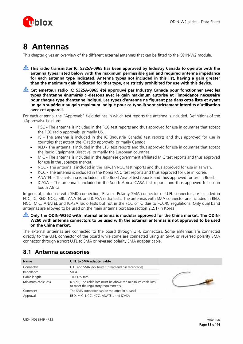
8.1 Antenna accessories Name U.FL to SMA adapter cable
Connector U.FL and SMA jack (outer thread and pin receptacle)
Impedance 50 Ω
Cable length 100-125 mm
Minimum cable loss 0.5 dB, The cable loss must be above the minimum cable loss to meet the regulatory requirements
Comment The SMA connector can be mounted in a panel
Approval RED, MIC, NCC, KCC, ANATEL, and ICASA
ODIN-W2 series - Data Sheet
UBX-14039949 - R13 Antennas
Page 34 of 44
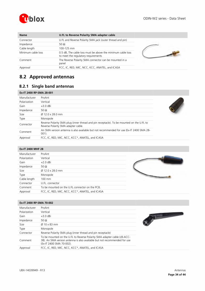
Name U.FL to Reverse Polarity SMA adapter cable
Connector U.FL and Reverse Polarity SMA jack (outer thread and pin)
Impedance 50 Ω
Cable length 100-125 mm
Minimum cable loss 0.5 dB, The cable loss must be above the minimum cable loss to meet the regulatory requirements
Comment The Reverse Polarity SMA connector can be mounted in a panel
Approval FCC, IC, RED, MIC, NCC, KCC, ANATEL, and ICASA
8.2 Approved antennas
8.2.1 Single band antennas Ex-IT 2400 RP-SMA 28-001
Manufacturer ProAnt
Polarization Vertical
Gain +3.0 dBi
Impedance 50 Ω
Size Ø 12.0 x 28.0 mm
Type Monopole
Connector Reverse Polarity SMA plug (inner thread and pin receptacle). To be mounted on the U.FL to Reverse Polarity SMA adapter cable.
Comment An SMA version antenna is also available but not recommended for use (Ex-IT 2400 SMA 28-001).
Approval FCC, IC, RED, MIC, NCC, KCC*, ANATEL, and ICASA
Ex-IT 2400 MHF 28
Manufacturer ProAnt
Polarization Vertical
Gain +2.0 dBi
Impedance 50 Ω
Size Ø 12.0 x 28.0 mm
Type Monopole
Cable length 100 mm
Connector U.FL. connector
Comment To be mounted on the U.FL connector on the PCB.
Approval FCC, IC, RED, MIC, NCC, KCC*, ANATEL, and ICASA
Ex-IT 2400 RP-SMA 70-002
Manufacturer ProAnt
Polarization Vertical
Gain +3.0 dBi
Impedance 50 Ω
Size Ø 10 x 83 mm
Type Monopole
Connector Reverse Polarity SMA plug (inner thread and pin receptacle)
Comment To be mounted on the U.FL to Reverse Polarity SMA adapter cable (cB-ACC-38). An SMA version antenna is also available but not recommended for use (Ex-IT 2400 SMA 70-002).
Approval FCC, IC, RED, MIC, NCC, KCC*, ANATEL, and ICASA
ODIN-W2 series - Data Sheet
UBX-14039949 - R13 Antennas
Page 35 of 44
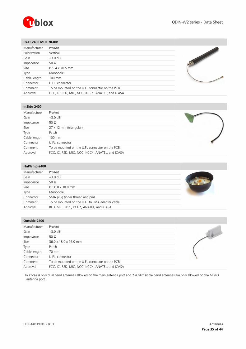
Ex-IT 2400 MHF 70-001
Manufacturer ProAnt
Polarization Vertical
Gain +3.0 dBi
Impedance 50 Ω
Size Ø 9.4 x 70.5 mm
Type Monopole
Cable length 100 mm
Connector U.FL. connector
Comment To be mounted on the U.FL connector on the PCB.
Approval FCC, IC, RED, MIC, NCC, KCC*, ANATEL, and ICASA
InSide-2400
Manufacturer ProAnt
Gain +3.0 dBi
Impedance 50 Ω
Size 27 x 12 mm (triangular)
Type Patch
Cable length 100 mm
Connector U.FL. connector
Comment To be mounted on the U.FL connector on the PCB.
Approval FCC, IC, RED, MIC, NCC, KCC*, ANATEL, and ICASA
FlatWhip-2400
Manufacturer ProAnt
Gain +3.0 dBi
Impedance 50 Ω
Size Ø 50.0 x 30.0 mm
Type Monopole
Connector SMA plug (inner thread and pin)
Comment To be mounted on the U.FL to SMA adapter cable.
Approval RED, MIC, NCC, KCC*, ANATEL, and ICASA
Outside-2400
Manufacturer ProAnt
Gain +3.0 dBi
Impedance 50 Ω
Size 36.0 x 18.0 x 16.0 mm
Type Patch
Cable length 70 mm
Connector U.FL. connector
Comment To be mounted on the U.FL connector on the PCB.
Approval FCC, IC, RED, MIC, NCC, KCC*, ANATEL, and ICASA
* In Korea is only dual band antennas allowed on the main antenna port and 2.4 GHz single band antennas are only allowed on the MIMO antenna port.
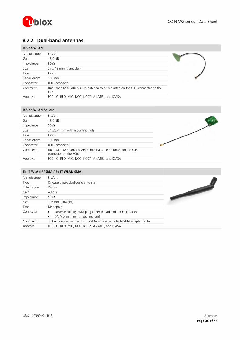
ODIN-W2 series - Data Sheet
UBX-14039949 - R13 Antennas
Page 36 of 44
8.2.2 Dual-band antennas InSide-WLAN
Manufacturer ProAnt
Gain +3.0 dBi
Impedance 50 Ω
Size 27 x 12 mm (triangular)
Type Patch
Cable length 100 mm
Connector U.FL. connector
Comment Dual-band (2.4 GHz/ 5 GHz) antenna to be mounted on the U.FL connector on the PCB.
Approval FCC, IC, RED, MIC, NCC, KCC*, ANATEL, and ICASA
InSide-WLAN Square
Manufacturer ProAnt
Gain +3.0 dBi
Impedance 50 Ω
Size 24x22x1 mm with mounting hole
Type Patch
Cable length 100 mm
Connector U.FL. connector
Comment Dual-band (2.4 GHz / 5 GHz) antenna to be mounted on the U.FL connector on the PCB.
Approval FCC, IC, RED, MIC, NCC, KCC*, ANATEL, and ICASA
Ex-IT WLAN RPSMA / Ex-IT WLAN SMA
Manufacturer ProAnt
Type ½ wave dipole dual-band antenna
Polarization Vertical
Gain +3 dBi
Impedance 50 Ω
Size 107 mm (Straight)
Type Monopole
Connector • Reverse Polarity SMA plug (inner thread and pin receptacle) • SMA plug (inner thread and pin)
Comment To be mounted on the U.FL to SMA or reverse polarity SMA adapter cable.
Approval FCC, IC, RED, MIC, NCC, KCC*, ANATEL, and ICASA

ODIN-W2 series - Data Sheet
UBX-14039949 - R13 Product handling and soldering
Page 37 of 44
9 Product handling and soldering
9.1 Packaging
9.2 Packaging The ODIN-W2 series modules are delivered as hermetically sealed, reeled tapes to enable efficient production, production lot set-up and tear-down. For more information about packaging, see the u-blox Package Information Guide [3].
9.2.1 Reels The ODIN-W2 series modules are delivered on the reel as described in Table 29:
Parameter Specification
Reel type B2
Delivery quantity 200
Table 29: Reel information for ODIN-W2 series modules
9.2.2 Tapes Figure 8 shows the position and the orientation of ODIN-W2 modules as they are delivered on the tape, while Figure 9 specifies the tape dimensions.
Figure 8: Orientation for ODIN-W2 modules on tape
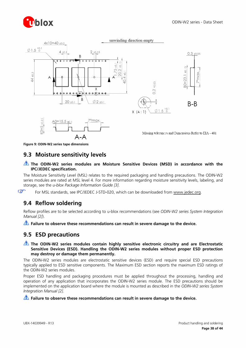
ODIN-W2 series - Data Sheet
UBX-14039949 - R13 Product handling and soldering
Page 38 of 44
Figure 9: ODIN-W2 series tape dimensions
9.3 Moisture sensitivity levels
The ODIN-W2 series modules are Moisture Sensitive Devices (MSD) in accordance with the IPC/JEDEC specification.
The Moisture Sensitivity Level (MSL) relates to the required packaging and handling precautions. The ODIN-W2 series modules are rated at MSL level 4. For more information regarding moisture sensitivity levels, labeling, and storage, see the u-blox Package Information Guide [3].
For MSL standards, see IPC/JEDEC J-STD-020, which can be downloaded from www.jedec.org.
9.4 Reflow soldering Reflow profiles are to be selected according to u-blox recommendations (see ODIN-W2 series System Integration Manual [2]).
Failure to observe these recommendations can result in severe damage to the device.
9.5 ESD precautions
The ODIN-W2 series modules contain highly sensitive electronic circuitry and are Electrostatic Sensitive Devices (ESD). Handling the ODIN-W2 series modules without proper ESD protection may destroy or damage them permanently.
The ODIN-W2 series modules are electrostatic sensitive devices (ESD) and require special ESD precautions typically applied to ESD sensitive components. The Maximum ESD section reports the maximum ESD ratings of the ODIN-W2 series modules.
Proper ESD handling and packaging procedures must be applied throughout the processing, handling and operation of any application that incorporates the ODIN-W2 series module. The ESD precautions should be implemented on the application board where the module is mounted as described in the ODIN-W2 series System Integration Manual [2].
Failure to observe these recommendations can result in severe damage to the device.
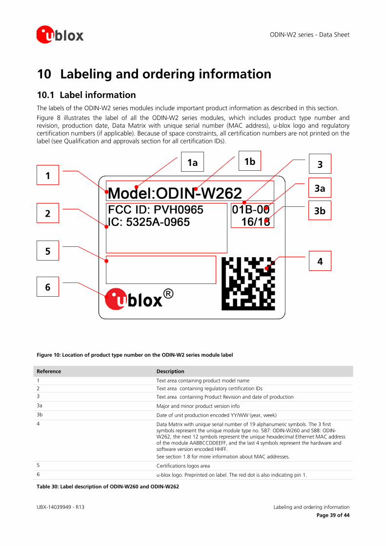
ODIN-W2 series - Data Sheet
UBX-14039949 - R13 Labeling and ordering information
Page 39 of 44
10 Labeling and ordering information
10.1 Label information The labels of the ODIN-W2 series modules include important product information as described in this section.
Figure 8 illustrates the label of all the ODIN-W2 series modules, which includes product type number and revision, production date, Data Matrix with unique serial number (MAC address), u-blox logo and regulatory certification numbers (if applicable). Because of space constraints, all certification numbers are not printed on the label (see Qualification and approvals section for all certification IDs).
Figure 10: Location of product type number on the ODIN-W2 series module label
Reference Description
1 Text area containing product model name
2 Text area containing regulatory certification IDs
3 Text area containing Product Revision and date of production
3a Major and minor product version info
3b Date of unit production encoded YY/WW (year, week)
4 Data Matrix with unique serial number of 19 alphanumeric symbols. The 3 first symbols represent the unique module type no. 587: ODIN-W260 and 588: ODIN-W262, the next 12 symbols represent the unique hexadecimal Ethernet MAC address of the module AABBCCDDEEFF, and the last 4 symbols represent the hardware and software version encoded HHFF. See section 1.8 for more information about MAC addresses.
5 Certifications logos area
6 u-blox logo. Preprinted on label. The red dot is also indicating pin 1.
Table 30: Label description of ODIN-W260 and ODIN-W262
3a 1
2 3b
4
3 1a 1b
5
6
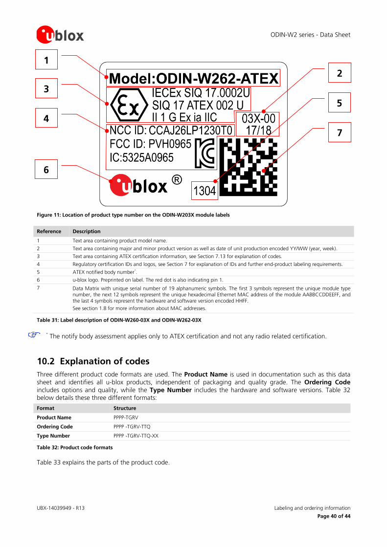
ODIN-W2 series - Data Sheet
UBX-14039949 - R13 Labeling and ordering information
Page 40 of 44
Figure 11: Location of product type number on the ODIN-W203X module labels
Reference Description
1 Text area containing product model name.
2 Text area containing major and minor product version as well as date of unit production encoded YY/WW (year, week).
3 Text area containing ATEX certification information, see Section 7.13 for explanation of codes.
4 Regulatory certification IDs and logos, see Section 7 for explanation of IDs and further end-product labeling requirements.
5 ATEX notified body number*.
6 u-blox logo. Preprinted on label. The red dot is also indicating pin 1.
7 Data Matrix with unique serial number of 19 alphanumeric symbols. The first 3 symbols represent the unique module type number, the next 12 symbols represent the unique hexadecimal Ethernet MAC address of the module AABBCCDDEEFF, and the last 4 symbols represent the hardware and software version encoded HHFF. See section 1.8 for more information about MAC addresses.
Table 31: Label description of ODIN-W260-03X and ODIN-W262-03X
* The notify body assessment applies only to ATEX certification and not any radio related certification.
10.2 Explanation of codes Three different product code formats are used. The Product Name is used in documentation such as this data sheet and identifies all u-blox products, independent of packaging and quality grade. The Ordering Code includes options and quality, while the Type Number includes the hardware and software versions. Table 32 below details these three different formats:
Format Structure
Product Name PPPP-TGRV
Ordering Code PPPP -TGRV-TTQ
Type Number PPPP -TGRV-TTQ-XX
Table 32: Product code formats
Table 33 explains the parts of the product code.
1
3
4
6
2
5
7
ODIN-W2 series - Data Sheet
UBX-14039949 - R13 Labeling and ordering information
Page 41 of 44
Code Meaning Example
PPPP Form factor ODIN
TG Platform (Technology and Generation) T – Dominant technology, For example, W: Wi-Fi, B: Bluetooth G - Generation
W2: Wi-Fi Generation 2
R Wireless technology; range [0...9] 6: Multi-radio dual-band 2.4+5GHz
V Variant based on the same platform; range [00…99] 0: default mounting, with connector for external antenna
TT Major Product Version 00: first revision
Q Quality grade
• A: Automotive
• B: Professional
• C: Standard
• X: ATEX
B: professional grade
XX Minor product version (not relevant for certification) Default value is 00
Table 33: Part identification code
10.3 Ordering information Ordering Code Product
ODIN-W260-00B Wi-Fi IEEE802.11a/b/g/n (dual-band) 2.4 GHz 2x2 MIMO and Bluetooth dual-mode module with dual U.FL. coaxial antenna connectors. Software 1.0.0
ODIN-W262-00B Wi-Fi IEEE802.11a/b/g/n (dual-band) and Bluetooth dual-mode module with internal dual-band antenna. Software 1.0.0
ODIN-W260-01B Wi-Fi IEEE802.11a/b/g/n (dual-band) 2.4 GHz 2x2 MIMO and Bluetooth dual-mode module with dual U.FL. coaxial antenna connectors. Software 2.0.2
ODIN-W262-01B Wi-Fi IEEE802.11a/b/g/n (dual-band) and Bluetooth dual-mode module with internal dual-band antenna. Software 2.0.2
ODIN-W260-02B Wi-Fi IEEE802.11a/b/g/n (dual-band) 2.4 GHz 2x2 MIMO and Bluetooth dual-mode module with dual U.FL. coaxial antenna connectors. u-blox connectivity software version 3.0.1
ODIN-W262-02B Wi-Fi IEEE802.11a/b/g/n (dual-band) and Bluetooth dual-mode module with internal dual-band antenna. u-blox connectivity software version 3.0.1
ODIN-W260-03B Wi-Fi IEEE802.11a/b/g/n (dual-band) 2.4 GHz 2x2 MIMO and Bluetooth dual-mode module with dual U.FL. coaxial antenna connectors. Software 4.0.1
ODIN-W262-03B Wi-Fi IEEE802.11a/b/g/n (dual-band) and Bluetooth dual-mode module with internal dual-band antenna. Software 4.0.1
ODIN-W260-03X ATEX certified Wi-Fi IEEE802.11a/b/g/n (dual-band) 2.4 GHz 2x2 MIMO and Bluetooth dual mode module with dual U.FL. coaxial antenna connectors. u-blox connectivity software version 4.0.1
ODIN-W262-03X ATEX certified Wi-Fi IEEE802.11a/b/g/n (dual-band) and Bluetooth dual mode module with internal dual-band antenna. u-blox connectivity software version 4.0.1
Table 34: Product ordering codes
ODIN-W2 series - Data Sheet
UBX-14039949 - R13 Appendix
Page 42 of 44
Appendix
Glossary Name Definition
ADC Analog to Digital Converter
BT Bluetooth
CAN Controller Area Network
CTS Clear To Send
DC Direct Current
DoC Declaration of Conformity
DSR Data Set Ready
DTR Data Terminal Ready
EIRP Equivalent Isotropically Radiated Power
FW Firmware
GND Ground
GPIO General Purpose Input Output
H High
HW Hardware
I Input (means that this is an input port of the module)
IEEE Institute of Electrical and Electronics Engineers
L Low
LPO Low Power Oscillator
MIMO Multi-Input Multi-Output
N/A Not Applicable
O Output (means that this is an output port of the module)
PCN / IN Product Change Notification / Information Note
PD Pull-Down
PU Pull-Up
RMII Reduced Media Independent Interface
RTS Request To Send
RXD Receive Data
SMI Station Management Interface
SPI Serial Peripheral Interface
TBD To Be Defined
TXD Transmit Data
UART Universal Asynchronous Receiver-Transmitter serial interface
Table 35: Explanation of abbreviations used
ODIN-W2 series - Data Sheet
UBX-14039949 - R13 Related documents
Page 43 of 44
Related documents [1] u-blox Short Range Modules AT Commands Manual, document number UBX-14044127
[2] ODIN-W2 series System Integration Manual, document number UBX-14040040
[3] u-blox Package Information Guide, document number UBX-14001652
[4] ODIN-W2 Declaration of Conformity, document number, UBX-15024695
For regular updates to u-blox documentation and to receive product change notifications please register on our homepage.
Revision history
Revision Date Name Comments
R01 05-Sep-2014 mwej Initial release.
R02 16-Feb-2015 fbro Minor updates
R03 23-Apr-2015 ajoh Updated features list, added input from early measurements and label specification.
R04 08-July-2015 fbro, kgom Applied u-blox word template.
R05 22-Sept-2015 mwej, kgom Major updates. Updated some IO voltage levels and some tolerances. Clarified mechanical outline. Updated performance measurements with ODIN-W26x SPA FW v0.11.05. Updated after type approval with approval information. Updated Table 1 similar to the ODIN-W2 series Product Summary.
R06 29-Jan-2016 mwej, pber Added ETSI, FCC, IC, Japan approval certification information. Added Bluetooth Qualification information. Added list of approved antennas. Removed two unavailable test points from Mechanical dimensions (correction). Provided reference to ODIN-W2 Declaration of Conformity (UBX-15024695). Changed Document status to Early Production Information. Removed n rate characteristics (will be added when supported). Modified Table 1 and Table 2. Updated section 1.1 and section 5.4 (values in Table 19 to Table 26).
R07 16-Jun-2016 mwej, kgom Updated product features (Table 1). Modified Updated to product version ODIN-W260-01B and ODIN-W262-01B due to firmware update. Updated label (section 10.2). Added MAC address information (section 1.8). Power saving mode implemented and current consumption reduced in idle mode (modified Table 14 - Table 18). Added Taiwan, China and Korea approval certification information (section 7.8 and section 8). Updated order information (Table 34).
R08 18-Jul-2016 mwej, kgom Updated product features (Table 1). Added compliance information for Australia and New Zealand (section 7.9).
R09 06-Oct-2016 mwej, kgom Updated the Product features (Table 1) and applicable products Table (page 2) with Firmware 3.0. Added antenna type information in section 8.2. Updated Australia and New Zealand compliance information (section 7.9) and tape orientation (section 9.2.2). Removed the information in European Union regulatory compliance (section 7.2) and provided reference to the ODIN-W2 Declaration of Conformity (UBX-15024695).
R10 02-Dec-2016 mwej Updated the document status to “Production Information”. Updated number of Test points (TP) to 51 in Figure 5. Removed reference to System Integration Manual [2] in section 7.5. Added channel information in Access Point mode (Table 2). Added information about support for IEEE 802.11d/e/i/h (h:DFS client only) in Table 2.
R11 10-Jan-2017 ajoh, ecar, kgom Updated Product ordering codes (Table 34). Included support for ODIN-W2 firmware versions – 2.0.2 and 3.0.1. On page 2, replaced Document status with Disclosure restriction.
R12 30-Mar-2017 mwej Updated Product ordering codes (Table 34). Included support for ODIN-W2 firmware version – 4.0.0. Added type approval information for Brazil and South Africa (chapters 7 and 8).
R13 1-Sep-2017 mwej, kgom Included support for ODIN-W2 software version 4.0.1. Updated Table 1, section 7.13, and section 10. Added information about cable length limitation (section 2 and 8.1). Replaced R&TTE with RED (chapter 8). Replaced firmware with software.
ODIN-W2 series - Data Sheet
UBX-14039949 - R13 Contact
Page 44 of 44
Contact For complete contact information visit us at www.u-blox.com
u-blox Offices
North, Central and South America
u-blox America, Inc.
Phone: +1 703 483 3180 E-mail: [email protected]
Regional Office West Coast:
Phone: +1 408 573 3640 E-mail: [email protected]
Technical Support:
Phone: +1 703 483 3185 E-mail: support @u-blox.com
Headquarters Europe, Middle East, Africa
u-blox AG
Phone: +41 44 722 74 44 E-mail: [email protected] Support: [email protected]
Asia, Australia, Pacific
u-blox Singapore Pte. Ltd.
Phone: +65 6734 3811 E-mail: [email protected] Support: [email protected]
Regional Office Australia: Phone: +61 2 8448 2016 E-mail: [email protected] Support: [email protected]
Regional Office China (Beijing):
Phone: +86 10 68 133 545 E-mail: [email protected] Support: [email protected]
Regional Office China (Chongqing):
Phone: +86 23 6815 1588 E-mail: [email protected] Support: [email protected]
Regional Office China (Shanghai):
Phone: +86 21 6090 4832 E-mail: [email protected] Support: [email protected]
Regional Office China (Shenzhen):
Phone: +86 755 8627 1083 E-mail: [email protected] Support: [email protected]
Regional Office India:
Phone: +91 80 4050 9200 E-mail: [email protected] Support: [email protected]
Regional Office Japan (Osaka):
Phone: +81 6 6941 3660 E-mail: [email protected] Support: [email protected]
Regional Office Japan (Tokyo):
Phone: +81 3 5775 3850 E-mail: [email protected] Support: [email protected]
Regional Office Korea:
Phone: +82 2 542 0861 E-mail: [email protected] Support: [email protected]
Regional Office Taiwan:
Phone: +886 2 2657 1090 E-mail: [email protected] Support: [email protected]