octal squib driver asic for safety application · octal squib driver asic for safety application...
TRANSCRIPT

September 2013 Doc ID 022048 Rev 2 1/51
1
L9659
Octal squib driver ASIC for safety application
Features■ 8 deployment drivers with SPI selectable firing
current and times
■ Capability to deploy the squib with 1.2 A (min)/2 ms, 1.75 A (min)/1.0 ms and 1.75 A (min)/0.65 ms between VRES of 7 V to 37 V
■ Capability to deploy the squib with 1.5 A (min)/2 ms between VRES of 7 V to 25 V
■ Firing capability to deploy all channels simultaneously
■ Independently controlled high-side and low-side MOS for diagnosis
■ Analog output available for resistance measurement
■ Squib short to ground, short to battery and MOS diagnostic available on SPI register
■ Capability to deploy the squib the low side MOS is shorted to ground
■ 4 fire enable inputs
■ 5.5 MHz SPI interface
■ Low voltage internal reset
■ 2 kV ESD capability on all pins
■ Package: LQFP64
■ Technology: ST proprietary BCD5 (0.65 µm)
■ RoHS compliant
DescriptionThe L9659 is intended to deploy up to 8 squibs. Squib drivers are sized to deploy 1.2 A minimum for 2 ms, 1.75 A minimum for 1 ms and 1.75 A minimum for 0.65 ms during load dump along with 1.5 A minimum for 2 ms for VRES voltages less than 25 V.
Full diagnostic capabilities of the squib interface are provided.
LQFP64 (10x10x1.4mm)
Table 1. Device summary
Order code Amb. temp range, C Package Packing
L9659 -40 to +95 LQFP64 Tray
L9659TR -40 to +95 LQFP64 Tape and reel
www.st.com

Contents L9659
2/51 Doc ID 022048 Rev 2
Contents
1 Block diagram and pin description . . . . . . . . . . . . . . . . . . . . . . . . . . . . . 5
1.1 Block diagram . . . . . . . . . . . . . . . . . . . . . . . . . . . . . . . . . . . . . . . . . . . . . . . 5
1.2 Pin description . . . . . . . . . . . . . . . . . . . . . . . . . . . . . . . . . . . . . . . . . . . . . . 5
1.3 Application schematic . . . . . . . . . . . . . . . . . . . . . . . . . . . . . . . . . . . . . . . . . 8
2 Electrical specifications . . . . . . . . . . . . . . . . . . . . . . . . . . . . . . . . . . . . . . 9
2.1 Absolute maximum ratings . . . . . . . . . . . . . . . . . . . . . . . . . . . . . . . . . . . . . 9
2.2 Absolute maximum degraded operating ratings . . . . . . . . . . . . . . . . . . . . 10
2.3 Operating ratings . . . . . . . . . . . . . . . . . . . . . . . . . . . . . . . . . . . . . . . . . . . 10
2.4 Electrical characteristics . . . . . . . . . . . . . . . . . . . . . . . . . . . . . . . . . . . . . . 11
2.4.1 General . . . . . . . . . . . . . . . . . . . . . . . . . . . . . . . . . . . . . . . . . . . . . . . . . 11
2.4.2 Electrical characteristics - Squib deployment drivers and diagnostics . . 12
2.4.3 SPI timing . . . . . . . . . . . . . . . . . . . . . . . . . . . . . . . . . . . . . . . . . . . . . . . 17
3 Functional description . . . . . . . . . . . . . . . . . . . . . . . . . . . . . . . . . . . . . . 19
3.1 Overview . . . . . . . . . . . . . . . . . . . . . . . . . . . . . . . . . . . . . . . . . . . . . . . . . 19
3.2 General functions . . . . . . . . . . . . . . . . . . . . . . . . . . . . . . . . . . . . . . . . . . . 19
3.2.1 Power on reset (POR) . . . . . . . . . . . . . . . . . . . . . . . . . . . . . . . . . . . . . . 19
3.2.2 RESETB . . . . . . . . . . . . . . . . . . . . . . . . . . . . . . . . . . . . . . . . . . . . . . . . 19
3.2.3 Reference resistor . . . . . . . . . . . . . . . . . . . . . . . . . . . . . . . . . . . . . . . . . 20
3.2.4 Loss of ground . . . . . . . . . . . . . . . . . . . . . . . . . . . . . . . . . . . . . . . . . . . . 20
3.2.5 VRESx capacitance . . . . . . . . . . . . . . . . . . . . . . . . . . . . . . . . . . . . . . . . 20
3.2.6 Supply voltages . . . . . . . . . . . . . . . . . . . . . . . . . . . . . . . . . . . . . . . . . . . 20
3.2.7 Ground connections . . . . . . . . . . . . . . . . . . . . . . . . . . . . . . . . . . . . . . . . 20
3.3 Serial peripheral interface (SPI) . . . . . . . . . . . . . . . . . . . . . . . . . . . . . . . . 21
3.3.1 SPI pin descriptions . . . . . . . . . . . . . . . . . . . . . . . . . . . . . . . . . . . . . . . . 21
3.4 Squib drivers . . . . . . . . . . . . . . . . . . . . . . . . . . . . . . . . . . . . . . . . . . . . . . 22
3.4.1 Firing . . . . . . . . . . . . . . . . . . . . . . . . . . . . . . . . . . . . . . . . . . . . . . . . . . . 22
3.4.2 Firing current measurement . . . . . . . . . . . . . . . . . . . . . . . . . . . . . . . . . . 25
3.4.3 Fire enable (FEN) function description . . . . . . . . . . . . . . . . . . . . . . . . . 26
3.4.4 Squib diagnostics . . . . . . . . . . . . . . . . . . . . . . . . . . . . . . . . . . . . . . . . . . 27
3.4.5 SPI register definition for squib functions . . . . . . . . . . . . . . . . . . . . . . . . 31
4 Package information . . . . . . . . . . . . . . . . . . . . . . . . . . . . . . . . . . . . . . . . 49
5 Revision history . . . . . . . . . . . . . . . . . . . . . . . . . . . . . . . . . . . . . . . . . . . 50

L9659 List of tables
Doc ID 022048 Rev 2 3/51
List of tables
Table 1. Device summary . . . . . . . . . . . . . . . . . . . . . . . . . . . . . . . . . . . . . . . . . . . . . . . . . . . . . . . . . . 1Table 2. Pin description . . . . . . . . . . . . . . . . . . . . . . . . . . . . . . . . . . . . . . . . . . . . . . . . . . . . . . . . . . . 5Table 3. Absolute maximum ratings . . . . . . . . . . . . . . . . . . . . . . . . . . . . . . . . . . . . . . . . . . . . . . . . . . 9Table 4. Absolute maximum degraded operating ratings . . . . . . . . . . . . . . . . . . . . . . . . . . . . . . . . . 10Table 5. Operating ratings . . . . . . . . . . . . . . . . . . . . . . . . . . . . . . . . . . . . . . . . . . . . . . . . . . . . . . . . 10Table 6. General - DC electrical characteristics . . . . . . . . . . . . . . . . . . . . . . . . . . . . . . . . . . . . . . . . 11Table 7. Squib deployment drivers and diagnostics - DC electrical characteristics . . . . . . . . . . . . . 12Table 8. SPI timing - DC electrical characteristics . . . . . . . . . . . . . . . . . . . . . . . . . . . . . . . . . . . . . . 17Table 9. Features that are accessed/controlled for the SPI . . . . . . . . . . . . . . . . . . . . . . . . . . . . . . . 21Table 10. SPI MOSI/MISO response . . . . . . . . . . . . . . . . . . . . . . . . . . . . . . . . . . . . . . . . . . . . . . . . . 25Table 11. How faults shall be interpreted . . . . . . . . . . . . . . . . . . . . . . . . . . . . . . . . . . . . . . . . . . . . . . 28Table 12. Diagnostic Mode HSS selection . . . . . . . . . . . . . . . . . . . . . . . . . . . . . . . . . . . . . . . . . . . . . 30Table 13. Diagnostic mode 3 VRESx selection . . . . . . . . . . . . . . . . . . . . . . . . . . . . . . . . . . . . . . . . . 30Table 14. MISO responses to various events. . . . . . . . . . . . . . . . . . . . . . . . . . . . . . . . . . . . . . . . . . . 31Table 15. Command description summary . . . . . . . . . . . . . . . . . . . . . . . . . . . . . . . . . . . . . . . . . . . . . 32Table 16. Configuration mode 1 . . . . . . . . . . . . . . . . . . . . . . . . . . . . . . . . . . . . . . . . . . . . . . . . . . . . . 33Table 17. Configuration mode 2 . . . . . . . . . . . . . . . . . . . . . . . . . . . . . . . . . . . . . . . . . . . . . . . . . . . . . 34Table 18. Deployment mode 1 bit definition . . . . . . . . . . . . . . . . . . . . . . . . . . . . . . . . . . . . . . . . . . . . 35Table 19. Deployment mode 2 bit definition . . . . . . . . . . . . . . . . . . . . . . . . . . . . . . . . . . . . . . . . . . . . 36Table 20. Diagnostic selection . . . . . . . . . . . . . . . . . . . . . . . . . . . . . . . . . . . . . . . . . . . . . . . . . . . . . . 40Table 21. Diagnostic mode LS FET selection. . . . . . . . . . . . . . . . . . . . . . . . . . . . . . . . . . . . . . . . . . . 40Table 22. Diagnostic mode HS FET selection . . . . . . . . . . . . . . . . . . . . . . . . . . . . . . . . . . . . . . . . . . 41Table 23. Diagnostic mode HSS selection . . . . . . . . . . . . . . . . . . . . . . . . . . . . . . . . . . . . . . . . . . . . . 41Table 24. Diagnostic mode VRESx selection . . . . . . . . . . . . . . . . . . . . . . . . . . . . . . . . . . . . . . . . . . . 41Table 25. Channel selection . . . . . . . . . . . . . . . . . . . . . . . . . . . . . . . . . . . . . . . . . . . . . . . . . . . . . . . . 42Table 26. MOSI diagnostic mode 1 bit definition . . . . . . . . . . . . . . . . . . . . . . . . . . . . . . . . . . . . . . . . 43Table 27. DEPLOY_STATUSx flag and the DEPLOY_SUCCESSx flag conditions. . . . . . . . . . . . . . 44Table 28. MOSI monitor mode 2 Bit definition . . . . . . . . . . . . . . . . . . . . . . . . . . . . . . . . . . . . . . . . . . 45Table 29. Current measurement channel selections . . . . . . . . . . . . . . . . . . . . . . . . . . . . . . . . . . . . . 45Table 30. MOSI monitor mode 3 bit definition . . . . . . . . . . . . . . . . . . . . . . . . . . . . . . . . . . . . . . . . . . 46Table 31. MOSI monitor mode 4 bit definition . . . . . . . . . . . . . . . . . . . . . . . . . . . . . . . . . . . . . . . . . . 48Table 32. Document revision history . . . . . . . . . . . . . . . . . . . . . . . . . . . . . . . . . . . . . . . . . . . . . . . . . 50

List of figures L9659
4/51 Doc ID 022048 Rev 2
List of figures
Figure 1. Block diagram . . . . . . . . . . . . . . . . . . . . . . . . . . . . . . . . . . . . . . . . . . . . . . . . . . . . . . . . . . . . 5Figure 2. Application schematic . . . . . . . . . . . . . . . . . . . . . . . . . . . . . . . . . . . . . . . . . . . . . . . . . . . . . . 8Figure 3. MOS settling time and turn-on time 2 . . . . . . . . . . . . . . . . . . . . . . . . . . . . . . . . . . . . . . . . . 16Figure 4. SPI timing diagram . . . . . . . . . . . . . . . . . . . . . . . . . . . . . . . . . . . . . . . . . . . . . . . . . . . . . . . 18Figure 5. MISO loading for disable time measurement . . . . . . . . . . . . . . . . . . . . . . . . . . . . . . . . . . . 18Figure 6. POR timing . . . . . . . . . . . . . . . . . . . . . . . . . . . . . . . . . . . . . . . . . . . . . . . . . . . . . . . . . . . . . 19Figure 7. Deployment drivers diagram. . . . . . . . . . . . . . . . . . . . . . . . . . . . . . . . . . . . . . . . . . . . . . . . 23Figure 8. Driver activation timing diagram . . . . . . . . . . . . . . . . . . . . . . . . . . . . . . . . . . . . . . . . . . . . . 24Figure 9. Squib diagnostics block diagram . . . . . . . . . . . . . . . . . . . . . . . . . . . . . . . . . . . . . . . . . . . . 27Figure 10. LQFP64 mechanical data and package dimensions. . . . . . . . . . . . . . . . . . . . . . . . . . . . . . 49

L9659 Block diagram and pin description
Doc ID 022048 Rev 2 5/51
1 Block diagram and pin description
1.1 Block diagram
Figure 1. Block diagram
1.2 Pin description
Table 2. Pin description
Pin # Pin name Description I/O type Reset state
1 MISO SPI data out Output Hi-Z
2 NC No connect - -
3 FEN1 Fire enable for channels 0 and 1 Input Pulldown
4 FEN2 Fire enable for channels 2 and 3 Input Pulldown
5 RESETB Reset pin Input Pullup
6 GND Ground (analog & digital) - -
7 VDD VDD supply voltage Input -

Block diagram and pin description L9659
6/51 Doc ID 022048 Rev 2
8 FEN3 Fire enable for channels 4 and 5 Input Pulldown
9 FEN4 Fire enable for channels 6 and 7 Input Pulldown
10 NC No connect - -
11 NC No connect - -
12 CS_D SPI chip select for deployment driver Input Pullup
13 MOSI SPI data in Input Hi-Z
14 NC No connect - -
15 NC No connect - -
16 SCLK SPI clock Input Hi-Z
17 GND4 Power ground for loop channel 4 - -
18 SQL4 Low side driver output for channel 4 Output Pulldown
19 SQH4 High side driver output for channel 4 Output Hi-Z
20 VRES4 Reserve voltage for loop channel 4 Input -
21 VRES5 Reserve voltage for loop channel 5 Input -
22 SQH5 High side driver output for channel 5 Output Hi-Z
23 SQL5 Low side driver output for channel 5 Output Pulldown
24 GND5 Power ground for loop channel 5 - -
25 GND6 Power ground for loop channel 6 - -
26 SQL6 Low side driver output for channel 6 Output Pulldown
27 SQH6 High side driver output for channel 6 Output Hi-Z
28 VRES6 Reserve voltage for loop channel 6 Input -
29 VRES7 Reserve voltage for loop channel 7 Input -
30 SQH7 High side driver output for channel 7 Output Hi-Z
31 SQL7 Low side driver output for channel 7 Output Pulldown
32 GND7 Power ground for loop channel 7 - -
33 TEST Test pin Input Pulldown
34 VSDIAG Supply for deployment driver diagnostics Input -
35 NC No connect - -
36 Reserved Factory testmode output - -
37 Reserved Factory testmode output - -
38 NC No connect - -
39 NC No connect - -
40 NC No connect - -
41 NC No connect - -
42 NC No connect - -
Table 2. Pin description (continued)
Pin # Pin name Description I/O type Reset state

L9659 Block diagram and pin description
Doc ID 022048 Rev 2 7/51
43 NC No connect - -
44 NC No connect - -
45 NC No connect - -
46 IREF External current reference resistor Output -
47 AGND Ground reference for AOUT - -
48 AOUT Analog output for loop diagnostics Output Hi-Z
49 GND3 Power ground for loop channel 3 - -
50 SQL3 Low side driver output for channel 3 Output Pulldown
51 SQH3 High side driver output for channel 3 Output Hi-Z
52 VRES3 Reserve voltage for loop channel 3 Input -
53 VRES2 Reserve voltage for loop channel 2 Input -
54 SQH2 High side driver output for channel 2 Output Hi-Z
55 SQL2 Low side driver output for channel 2 Output Pulldown
56 GND2 Power ground for loop channel 2 - -
57 GND1 Power ground for loop channel 1 - -
58 SQL1 Low side driver output for channel 1 Output Pulldown
59 SQH1 High side driver output for channel 1 Output Hi-Z
60 VRES1 Reserve voltage for loop channel 1 Input -
61 VRES0 Reserve voltage for loop channel 0 Input -
62 SQH0 High side driver output for channel 0 Output Hi-Z
63 SQL0 Low side driver output for channel 0 Output Pulldown
64 GND0 Power ground for loop channel 0 - -
Table 2. Pin description (continued)
Pin # Pin name Description I/O type Reset state

Block diagram and pin description L9659
8/51 Doc ID 022048 Rev 2
1.3 Application schematic
Figure 2. Application schematic

L9659 Electrical specifications
Doc ID 022048 Rev 2 9/51
2 Electrical specifications
2.1 Absolute maximum ratingsThe following maximum ratings are continuous absolute ratings; exceeding any one of these values may cause permanent damage to the integrated circuit.
Table 3. Absolute maximum ratings
Symbol Parameter Value Unit
VDD (1) Supply voltage - 0.3 to 5.5 V
VSDIAG Supply voltage for squib diagnostics - 0.3 to 40 V
VRESx VRES voltage (VRES0, VRES1, VRES2, VRES3, VRES4, VRES5, VRES6, VRES7)
- 0.3 to 40 V
SQHx Squib high side drivers (SQH0, SQH1, SQH2, SQH3, SQH4, SQH5, SQH6, SQH7)
- 0.6 to 40 V
SQLx Squib low side drivers (SQL0, SQL1, SQL2, SQL3, SQL4, SQL5, SQL6, SQL7)
- 0.3 to 40 V
TEST Test pin -0.3 to 40 V
VI Discrete input voltage (RESETB, CS_D, SCLK, MOSI, FEN1, FEN2, FEN3, FEN4, IREF)
- 0.3 to 5.5 V
VO Discrete output voltage (MISO, AOUT) - 0.3 to 5.5 V
AGND Analog output reference -0.3 to 5.5 V
GNDx Ground (GND0, GND1, GND2, GND3, GND4, GND5, GND6, GND7)
-0.3 to 5.5 V
Tj (2) Maximum steady-state junction temperature 150 °C
Tamb Ambient temperature -40 to 95 °C
Tstg Storage temperature -65 to 150 °C
Rth j amb Thermal resistance junction to ambient (on FR-4 board) 46 °C/W
The following maximum ratings are up to 48 hours; exceeding any one of these values for longer than a total time of 48 hours may cause permanent damage to the integrated circuit.
VDD Supply voltage - 0.3 to 6.0 V
VI Discrete input voltage (RESETB, CS_D, SCLK, MOSI, FEN1, FEN2, FEN3, FEN4, IREF)
- 0.3 to 6.0 V
VO Discrete output voltage (MISO, AOUT) - 0.3 to 6.0 V
AGND Analog output reference -0.3 to 6.0 V
GNDxGround (GND0, GND1, GND2, GND3, GND4, GND5, GND6, GND7)
-0.3 to 6.0 V
Tj (2) Maximum steady-state junction temperature 150 °C
Tamb Ambient temperature -40 to 95 °C
Tstg Storage temperature -65 to 150 °C
Rth j amb Thermal resistance junction to ambient (on FR-4 board) 46 °C/W
1. Exceeding a VDD of 5.1V during a deployment may cause damage
2. To allow for deployment the maximum steady state junction temperature cannot exceed 130°C. Under the operating ratings defined in section 2.3 the steady state junction temperature will not exceed 130°C.
Electrical specifications L9659
10/51 Doc ID 022048 Rev 2
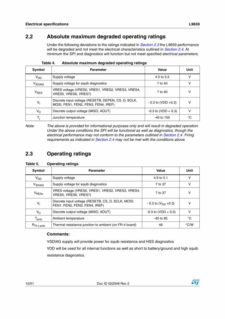
2.2 Absolute maximum degraded operating ratingsUnder the following deviations to the ratings indicated in Section 2.3 the L9659 performance will be degraded and not meet the electrical characteristics outlined in Section 2.4. At minimum the SPI and diagnostics will function but not meet specified electrical parameters.
Note: The above is provided for informational purposes only and will result in degraded operation. Under the above conditions the SPI will be functional as well as diagnostics, though the electrical performance may not conform to the parameters outlined in Section 2.4. Firing requirements as indicated in Section 2.4 may not be met with the conditions above.
2.3 Operating ratings
Comments:
VSDIAG supply will provide power for squib resistance and HSS diagnostics
VDD will be used for all internal functions as well as short to battery/ground and high squib
resistance diagnostics.
Table 4. Absolute maximum degraded operating ratings
Symbol Parameter Value Unit
VDD Supply voltage 4.5 to 5.5 V
VSDIAG Supply voltage for squib diagnostics 7 to 40 V
VRES VRES voltage (VRES0, VRES1, VRES2, VRES3, VRES4, VRES5, VRES6, VRES7)
7 to 40 V
VI Discrete input voltage (RESETB, DEPEN, CS_D, SCLK, MOSI, FEN1, FEN2, FEN3, FEN4, IREF)
- 0.3 to (VDD +0.3) V
VO Discrete output voltage (MISO, AOUT) -0.3 to (VDD + 0.3) V
Tj Junction temperature -40 to 150 °C
Table 5. Operating ratings
Symbol Parameter Value Unit
VDD Supply voltage 4.9 to 5.1 V
VSDIAG Supply voltage for squib diagnostics 7 to 37 V
VRESx VRES voltage (VRES0, VRES1, VRES2, VRES3, VRES4, VRES5, VRES6, VRES7)
7 to 37 V
VI Discrete input voltage (RESETB, CS_D, SCLK, MOSI, FEN1, FEN2, FEN3, FEN4, IREF)
- 0.3 to (VDD +0.3) V
VO Discrete output voltage (MISO, AOUT) -0.3 to (VDD + 0.3) V
Tamb Ambient temperature -40 to 95 °C
RTh j-amb Thermal resistance junction to ambient (on FR-4 board) 46 °C/W

L9659 Electrical specifications
Doc ID 022048 Rev 2 11/51
2.4 Electrical characteristics
2.4.1 General
4.9 V VDD 5.1 V; 7 V VRESX 37 V; 7 V VSDIAG 37 V; FEN1 = FEN2 = FEN3 = FEN4 = VDD; R_REF = 10 k, ±1 %, 100 PPM; -40 °C TA +95 °C; unless other specified.
Table 6. General - DC electrical characteristics
Symbol Parameter Test condition Min. Typ. Max. Unit
OscInternal oscillator frequency
Tested with 10K , 1%, 100ppm Iref resistor
4.75 - 5.25 MHz
VRST1
Internal voltage reset VDD after de-glitch time (tpor) See Figure 7
VDD level for L9659 to report reset condition -deployment drivers are disabled
4.0 - 4.5 V
VRST2Internal voltage reset VDD with no de-glitch time See
Guaranteed by design 2.1 - 3.0
tPOR POR De-glitch timer Timer for VRST1 5 - 25 µs
IDD Input current VDD
No squib diagnostics. No deployment. - - 15
mA
Resistance measurement diagnostics with no fault condition present.
- - 17
Short to –0.3V on SQL; VRCM active - - 35
During deployment - - 15
RIREF_HResistance threshold IREF
- - - 60.0 k
RIREF_L - 2.0 - - k
VIH_RESETBInput voltage threshold RESETB
- - - 2.0 V
VIL_RESETB - 0.8 - - V
VHYS_RST - 100 - 300 mV
VIH_TESTInput voltage threshold TEST
Guaranteed by design - 3.2 - V
ITESTPD Input pull-down current TEST 1.0 - 2.5 mA
IAOUT_SHRT AOUT pin current limit AOUT short to ground during squib resistance diagnostics
- - 20 mA
IRESETPUInput pull-up current RESETB
RESETB = VIH to GND -10 - -50 µA
IRESxQuiescent current for VRESx during HSS test
Current per pin during HSS test excluding selected channel
- - 10 µA
VIH Input voltage threshold (MOSI, SCLK, CS_D)
Input Logic = 1 - - 2.0 V
VIL Input Logic = 0 0.8 - - V
VHYSTInput hysteresis(MOSI, SCLK, CS_D)
100 - 300 mV
ILKGDInput leakage current MOSI, SCLK
VIN = VDD - - 1 µA
VIN = 0 to VIH -1 - - µA

Electrical specifications L9659
12/51 Doc ID 022048 Rev 2
2.4.2 Electrical characteristics - Squib deployment drivers and diagnostics
4.9 V VDD 5. 1V; 7 V VRESX 37 V; 7 V VSDIAG 37 V; FEN1 = FEN2 = FEN3 = FEN4 = VDD; R_REF = 10 k, ±1%, 100 PPM; -40 °C TA +95 °C; C_VRES0_1 68nF; C_VRES2_3 68nFC_VRES4_5 68nF; C_VRES6_7 68nF; unless other specified.
IPU_CS Input pull-up current CS_D VIN = VIH to GND -10 - -50 µA
VOHOutput voltage MISO
IOH = -800µA VDD–
0.8- - V
VOL IOL = 1.6mA - - 0.4 V
IHI_Z Tri-state current MISO MISO = VDD - - 1 µA
MISO = 0V -1 - - µA
Table 6. General - DC electrical characteristics (continued)
Symbol Parameter Test condition Min. Typ. Max. Unit
Table 7. Squib deployment drivers and diagnostics - DC electrical characteristics
Symbol Parameter Test condition Min. Typ. Max. Unit
General
ILKGSQH Leakage current SQH VSDIAG = VDD = 0,VRES = 37V, VSQH = 0V
- - 50 µA
ILKGVRES Bias current VRESX VSDIAG = 18V; VDD = 5V; VRES = 37V; SQH shorted to SQL
- - 10 µA
ILKGSQL Leakage current SQL VSDIAG = VDD = 0,VSQL = 18V
-10 - 10 µA
IPD Pulldown current SQL VSQL = 1.5V to 20V 3.3 - 4.1 mA
VBIAS Diagnostics Bias voltage Nominal 3.6V -5%VDD*0.72
+5% V
Short to battery/ground diagnostics - Rsqb from 0 to Open
ISVRCMMaximum diagnostics bias current limit
Short to battery or ground test active VSQH = 0V
5 - 20 mA
RSTBShort to battery resistance threshold
Vbatt = 6.5V 1.92 - 3.42 K
Vbatt = 16V 8.61 - 13.98 K
Vbatt = 20V 11.42 - 18.42 K
ISTBShort to battery current threshold
- 0.9 - 1.42 mA
RSTG Short to ground threshold - 1.07 - 2.1 K
ISTGShort to ground current threshold
- 1.8 - 3.2 mA

L9659 Electrical specifications
Doc ID 022048 Rev 2 13/51
tDIAGTIMEOUT Diagnostic delay time
From/CS until Test Results are Valid,Output voltage change 0V to VDD * 0.72CSQHx= 0.12µF
CSQLx= 0.12µF
- - 300 µs
High side safing diagnostics
ISRC_HSS
Diagnostic current into selected VRESx pin during test
Normal conditions 710 - 950 µA
IHSS_8 Current during diagnosticAll 8 VRESx pins tied together
710 - 1020 µA
RHSSNORM_th
Normal resistance range when running high side safing diagnostics
All 8 VRESx pins tied together
1.4 - 2.5 K
VHSSNORM_r
ange
Normal voltage range between VSDIAG and VRESx pin) when running high side safing diagnostics
All 8 VRESx pins tied together
1.0 - 2.5 V
VHSSSHORT_th
Short voltage threshold between VSDIAG and VRESx pin)
All 8 VRESx pins tied together
0.5 - 1.0 V
VHSSOPEN_th
Open voltage threshold between VSDIAG and VRESx pin)
All 8 VRESx pins tied together
2.5 - 4.0 V
tDIAGTIMEOUT Diagnostic delay time
From/CS until test results are valid,
CSQHx= 0.12µFCSQLx= 0.12µF
- - 500 µs
Voltage measurement diagnostics (VRESx)
IRESx Max diagnostic current into VRESx pin
Normal Conditions - - 50 µA
VVRESXLO_th Low voltage threshold for VRESx pin
- 5.0 - 7 V
VVRESXHI_th High voltage threshold for VRESx pin
- 13.7 - 18.0 V
tDIAGTIMEOUT Diagnostic delay time From/CS until test results are valid.
- - 100 µs
Table 7. Squib deployment drivers and diagnostics - DC electrical characteristics (continued)
Symbol Parameter Test condition Min. Typ. Max. Unit

Electrical specifications L9659
14/51 Doc ID 022048 Rev 2
MOS diagnostics
I_MOS MOS test max current Normal conditions - - ISVRCM mA
tSHUTOFF LS/HS MOS turn off under fault condition
Time is measured from the valid LS/ HS MOS current > 100mA to the LS/HS turn off
- - 4 µs
tFETtimeout FET timeout Normal Conditions - - 100 µs
High squib resistance diagnostics
RSQHIZ High load resistance threshold
- 1.07 - 2.1 k
IHR High resistance current threshold
- ISTG mA
tDIAGTIMEOUT MOS diagnostic delay time From/CS until test results are valid, CSQHx= 0.12µF CSQLx= 0.12µF
- - 300 µs
Squib resistance diagnostics
VOH
Output voltage AOUT
High saturation voltage;IAOUT = -500µA
VDD-0.2
- - V
VOL Low Saturation Voltage;IAOUT = +500µA
- - 0.2 V
IZ Tri-State Current AOUT AOUT = VDD - - 1 µA
AOUT = 0V -1 - µA
RSQB RANGE Load resistance range - 0 - 10.0
VAOUT
Resistance measurement analog output tolerance
VAOUT =
0 RSQB < 3.5 VAOUT-0.095V
-VAOUT+0.095V
V
3.5 RSQB 10 VAOUT·0.95V
-VAOUT·1.05V
V
ISRC Resistance measurement current source
VDD = 5.0V; VSDIAG = 7.0V to 37V
38 - 42 mA
ISINK Resistance measurement current sink
IPD OFF, VSQLx = 4 V 45 - 57 mA
ISLEW Rmeas current di/dt 30% - 70% of ISRC 2 - 11 mA/µs
VcmprVoltage threshold on squibpin to shutdown ISRC
- 2.65 - 3.25 V
tisrcshtdwn Shutdown time Guaranteed by design - - 30 µs
VLSDrsqbLSD (V_SQL) voltage during resistance measure
- 0.8 - 2.2 V
Table 7. Squib deployment drivers and diagnostics - DC electrical characteristics (continued)
Symbol Parameter Test condition Min. Typ. Max. Unit
VDD 19.75----------- 0.08
RSQB
--------------- +

L9659 Electrical specifications
Doc ID 022048 Rev 2 15/51
tR_WAIT Rmeas wait time
Wait time before AOUT voltage is stable for ADC reading R AOUT= 5.1k;CAOUT=10nF
- - 300 µs
FENx input pins
tFENfilter Minimum pulse width - 12 - 16 µs
IFENPD Internal pull-down current VIN = VIL to VDD 20 - 50 µA
VFENLO Input low voltage threshold - 0.8 - - V
VFENHI Input high voltage threshold - - - 2.0 V
TFENLATCH FEN Latch timer - 0 - 512 ms
tFLACCFEN latch timer
accuracy- - 20% - 20 %
Deployment drivers
TRESOLUTION Diagnostic timing / resolution IHS IMEAS, 0s TMEASURE_TIME 3.7ms
CSQUIB _HI = 0.12µF
CSQUIB _LO = 0.12µF
22.5 25 27.5 µs
TACCURACYDiagnostic time
acurracy- - 2 LSB
IMEAS High side driver current limit detect threshold
Guaranteed by design IHSX x 0.90
-IHSX x 0.99
A
RDSonTOTAL Total high and low side MOS on resistance
High side MOS + low side MOS D9:D8=”11”;VRES = 7V; I = 1.6A @95°C
- - 2.0
RDSonHS High side MOS on resistance D9:D8=”11”; VRES = 7V; Tamb = 95°C; IVRES = 1.6A;
- 0.3 0.8
RDSonLS Low side MOS on resistance - 0.6 1.2
IHS_12A
High side deployment current limit
Configuration mode 1 bits D9:D8=”00” SQHx shorted to ground;
VRES = 7 to 37V
1.21 - 1.47 A
IHS_15A
Configuration Mode 1 bits D9:D8=”01” SQHx shorted to ground;
VRES = 7 to 25V
1.51 - 1.85 A
IHS_175A
Configuration Mode 1 bits D9:D8=”11” SQHx shorted to ground;VRES = 7 to 37V
1.76 - 2.14 A
tILIM Low side MOS shutdown under short to battery
Vsqblo=18V 90 - 110 µs
ILS Low side MOS current limit 2.2 - 4.0 A
Table 7. Squib deployment drivers and diagnostics - DC electrical characteristics (continued)
Symbol Parameter Test condition Min. Typ. Max. Unit

Electrical specifications L9659
16/51 Doc ID 022048 Rev 2
Figure 3. MOS settling time and turn-on time 2
tsettle Firing current settling time
Time from fire command CS_D rising edge to where firing current remains within specified limits
CSQUIB _HI = 0 to 0.12µF
CSQUIB _LO = 0 to 0.12µF
- - 150 µs
tDEPLOY-2ms
Deployment time
VRES = 7Vto 37@ IHS_12A
VRES = 7Vto 25@ IHS_15A
For IHS_12A and IHS_15A Firing current measured from CS_D rising edge
2.15 - 2.5 ms
tDEPLOY-1ms
VRES = 7Vto 37V
For IHS_175A Firing current measured from CS_D rising edge
1.15 - 1.40 ms
tDEPLOY-0.65ms
VRES = 7Vto 37V
For IHS_175A Firing current measured from CS_D rising edge
0.65 - 0.85 ms
Table 7. Squib deployment drivers and diagnostics - DC electrical characteristics (continued)
Symbol Parameter Test condition Min. Typ. Max. Unit

L9659 Electrical specifications
Doc ID 022048 Rev 2 17/51
2.4.3 SPI timing
All SPI timing is performed with a 150 pF load on MISO unless otherwise noted
4.9V VDD 5.1V; 7V VRESX 37V; 7V VSDIAG 37V; FEN1 = FEN2 = FEN3 = FEN4 = VDD; R_REF = 10K, ±1%, 100PPM; -40°C TA +95°C; C_VRES0_1 68nF; C_VRES2_3 68nF; C_VRES4_5 68nF; C_VRES6_7 68nF; unless other specified.
.
Table 8. SPI timing - DC electrical characteristics
No. Symbol Parameter Min. Typ. Max. Unit
- fop Transfer frequency dc - 5.50 MHz
1 tSCK SCLK Period 181 - - ns
2 tLEAD Enable Lead Time 65 - - ns
3 tLAG Enable Lag Time 50 - - ns
4 tSCLKHS SCLK, High Time 65 - - ns
5 tSCLKLS SCLK, Low Time 65 - - ns
6 tSUS MOSI, Input Setup Time 20 - - ns
7 tHS MOSI, Input Hold Time 20 - - ns
8 tA MISO, Access Time - - 60 ns
9 tDIS (1) MISO, Disable Time - - 100 ns
10 tVS MISO, Output Valid Time - - 60 ns
11 tHO (1) MISO, Output Hold Time 0 - - ns
12 tRO Rise Time (Design Information) - - 30 ns
13 tFO Fall Time (Design Information) - - 30 ns
14 tCSN CS_D, Negated Time 640 - - ns
15 tCLKN
Time between CS rising edge and first transition of SCLK must be higher than tCLKN. It happens when multiple devices are connected to the same SCLK and MOSI but with different chip select.
500 - - ns
1. Parameters tDIS and tHO shall be measured with no additional capacitive load beyond the normal test fixture capacitance on the MISO pin. Additional capacitance during the disable time test erroneously extends the measured output disable time, and minimum capacitance on MISO is the worst case for output hold time.

Electrical specifications L9659
18/51 Doc ID 022048 Rev 2
Figure 4. SPI timing diagram
Figure 5. MISO loading for disable time measurement

L9659 Functional description
Doc ID 022048 Rev 2 19/51
3 Functional description
3.1 OverviewThe L9659 is an integrated circuit to be used in air bag systems. Its main functions include deployment of air bags. The L9659 supports 8 deployment loops.
3.2 General functions
3.2.1 Power on reset (POR)
The ASIC has a power on reset (POR) circuit, which monitors VDD voltage. When VDD voltage falls below VRST1 for longer than or equal to tPOR, all outputs are disabled and all internal registers are reset to their default condition. A second reset level, VRST2, also monitors VDD but uses no filter time and will disable all outputs and all internal registers are reset to their default condition when VDD falls below the reset threshold.
Figure 6. POR timing
3.2.2 RESETB
The RESETB pin is active low. The effects of RESETB are similar to those of a POR event, except during a deployment. When a deployment is in-progress, the L9659 will ignore the RESETB signal.
However, it will shut itself down as soon as it detects a POR condition. When the deployment is completed and RESETB signal is asserted, the L9659 disables its outputs and reset its internal registers to their default states.
A de-glitch timer is provided for the RESETB pin. The timer protects this pin against spurious glitches. The L9659 neglects RESETB signal if it is asserted for shorter than tGLITCH. RESETB has an internal pull-up in case of an open circuit.

Functional description L9659
20/51 Doc ID 022048 Rev 2
3.2.3 Reference resistor
IREF pin shall be connected to VDD supply through a resistor, RIREF. When the L9659 detects the resistor on IREF pin is larger than RIREF_H or smaller than RIREF_L, it goes into a reset condition. All outputs are disabled and all internal registers are reset to their default conditions.
3.2.4 Loss of ground
GND
When the GND pin is disconnected from PC-board ground, the L9659 goes in reset condition. All outputs are disabled and all internal registers are reset to their default conditions.
GND0-GND7
A loss of power-ground (GND0 – GND7) pin/s disables the respective low side driver/s on SQLx. However, the high side driver of the respective channel will still be able to be turned on. Thus under the scenario where the low side is shorted to ground the L9659 will be able to provide the programmed firing current for the specified time.
An open GNDx connection on any channel has no affect on the other channels. An open GNDx condition will be detected using the low side MOS diagnostics.
AGND
The AGND pin is a reference for AOUT pin. When AGND loses its connection, the voltage on AOUT pin is pulledup to VDD voltage and L9659 goes in reset condition. All outputs are disabled and all internal register are reset to their default conditions.
3.2.5 VRESx capacitance
To ensure all diagnostics function properly a typical capacitor of equal to or greater than 68nF is required close to the firing supply pins. Thus minimum of 4 capacitors are required with one placed close to the VRES0 and VRES1 pins and a second capacitor will be close to the VRES2 and VRES3 pins and a third capacitor will be close to the VRES4 and VRES5 pins and a forth capacitor will be close to the VRES6 and VRES7 pins.
3.2.6 Supply voltages
The primary current sources for the different functions of the ASIC are as follows:
● VRESx - Firing currents along with HSS and HS FET diagnostic currents
● VSDIAG - Squib resistance and HSS diagnostics
● VDD will be used for all internal functions as well as short to battery/ground and high squib resistance diagnostics.
3.2.7 Ground connections
GND pin (6) is not connected internally to other ground pins (AGND or power ground GNDx). A ground plane is needed to directly connect the GND pin. This ground plane needs to be isolated from the high current ground for the squib drivers to prevent voltage shifts.
AGND pin should be connected to ground plane too to minimize drop versus ground reference of ADC that capture AOUT voltage.

L9659 Functional description
Doc ID 022048 Rev 2 21/51
3.3 Serial peripheral interface (SPI)The L9659 contains one serial peripheral interfaces for control of the squib functions. The following table shows features that are accessed/controlled by the SPI.
.
The software reset accessed over SPI will reset squib functions. The L9659 has a counter to verify the number of clocks in SCLK. If the number of clocks in SCLK is not equal to 16 clocks while CS_D is asserted, it ignores the SPI message and sends a SPI fault response. L9659 computes SPI error length flag through counting the number ofSCLK rising edges occurring when CS_D is active. If the first SCLK rising edge occurs when CS_D is inactive and the falling edge occurs when CS_D is low, it is considered as valid edge.
MOSI commands contain several bits not used, all those bits must be 0. Commands are not recognized valid if one or more not used bits are not 0.
3.3.1 SPI pin descriptions
Chip select (CS_D)
Chip-select inputs select the L9659 for serial transfers. CS_D can be asserted at any given time and are active low. When chip-select is asserted, the respective MISO pin is released from tri-state mode, and all status information is latched into the SPI shift register. While chip-select is asserted, register data is shifted into MOSI pin and shifted out of MISO pin on each subsequent SCLK. When chip-select is negated, MISO pin is tri-stated. To allow sufficient time to reload the registers; chip-select pin shall remain negated for at least tCSN. The chip-select inputs have current sinks which pull these pins to the negated state when there is an open circuit condition. These pins have TTL level compatible input voltages allowing proper operation with microprocessors using a 3.3 to 5.0 volt supply.
Serial clock (SCLK)
SCLK input is the clock signal input for synchronization of serial data transfer. This pin has TTL level compatible input voltages allowing proper operation with microprocessors using a 3.3 to 5.0 volt supply. When chip select is asserted, both the SPI master and L9659 will latch input data on the rising edge of SCLK. The L9659 shifts data out on the falling edge of SCLK.
Serial data output (MISO)
MISO output pins shall be in one tri-state condition when chip select is negated. When chip select is asserted, the MSB is the first bit of the word/byte transmitted on MISO and the LSB is the last bit of the word/byte transmitted. This pin supplies a rail to rail output, so if interfaced to a microprocessor that is using a lower VDD supply, the appropriate microprocessor input pin shall not sink more than IOH(min) and shall not clamp the MISO output voltage to less than VOH(min) while MISO pin is in a logic “1” state. When connecting to a micro using a lower supply, such as 3.3V, a resistor divider shall be used with high enough impedance to prevent excess current flow.
Table 9. Features that are accessed/controlled for the SPI
Function Pin names Features accessed
Squib diagnostic and deployment SPI
SCLK
MISOMOSI
CS_D
All Squib Diagnostics; Squib related status information; Squib Arming and Firing; Software Reset; Component ID & Revision

Functional description L9659
22/51 Doc ID 022048 Rev 2
Serial data input (MOSI)
MOSI inputs take data from the master processor while chip select is asserted. The MSB shall be the first bit of each word/byte received on MOSI and the LSB shall be the last bit of each word/byte received.
This pin has TTL level compatible input voltages allowing proper operation with microprocessors using a 3.3 to 5.0 volt supply.
3.4 Squib drivers
3.4.1 Firing
The on-chip deployment drivers are designed to deliver 1.2A (min) for 2ms (min) and 1.75A (min) for 1ms (min)and 1.75A (min) for 0.65ms (min) with VRESx voltages between 7V and 37V. In addition the L9659 can provide 1.5A minimum for 2ms for VRESx voltages between 7V and 25V. The firing condition is selectable via the SPI. At the end of a deployment, a deploy success flag is asserted and can be read using the appropriate SPI command. Each VRESx and GNDx connection is used to accommodate 8 loops that can be deployed simultaneously.
Upon receiving a valid deployment condition, the respective SQHx and SQLx drivers are turned on. The only other activation of the SQHx and SQLx drivers is momentarily during a MOS diagnostic. Otherwise, SQHx and SQLx are inactive under any normal, fault, or transient conditions. Upon a successful deployment of the respective SQHx and SQLx drivers, a deploy command success flag is asserted via SPI. Refer to Figure 8. for the valid conditions and the deploy success flag timing.
The L9659 is protected against inadvertent turn on of the firing drivers unless the appropriate conditions are present. Non-typical conditions will not cause driver activation. This includes the case where VRESx and/or VSDIAG pins are connected to a supply up to 40V and VDD is between 0V and VDD min. Under these conditions the L9659 will ensure that driver activation will not occur. No flow of current shall be allowed through the SQHx and SQLx pins.

L9659 Functional description
Doc ID 022048 Rev 2 23/51
Figure 7. Deployment drivers diagram
Driver activation
The firing of a squib driver requires the appropriate FEN function to be active and two separate sixteen bit writes be made over the SPI. The FEN function is defined as the result of the FENx pin OR’d with the internal FENx latch. The FENx pin going high initiates the FEN function. With the FEN 1 function being active and the appropriate Arm and Fire commands sent then Squib_0 & 1 drivers would be activated. With the FEN 2 function being active and the appropriate Arm and Fire commands sent then Squib_2 & 3 drivers would be activated. With the FEN 3 function being active and the appropriate Arm and Fire commands sent then Squib_4 & 5 drivers would be activated. With the FEN 4 function being active and the appropriate Arm and Fire commands sent then Squib_6 & 7 drivers would be activated.
The first write is to ARM the drivers in preparation of receiving the fire command. The Arm command will stop on all channels any diagnostics that are active. Any combination of squibs can be armed. The second write is a FIRE command that must directly follow the Arm command and will activate the desired driver pairs assuming the FEN function is valid. If there is a parity mismatch the data bits will be ignored and the squib drivers will not have their status changed, and the two write sequence must then be started again. If there is a mismatch in channels selected then only those channels selected in both the Arm and Fire commands will be activated.

Functional description L9659
24/51 Doc ID 022048 Rev 2
During the first write, when the drivers are armed, all diagnostic functions are cleared. The FIRE command must follow the ARM command along with the FEN function active for driver activation. If a command is between the ARM and FIRE command then the sequence must be restarted. An error response will be received for the Fire command if the ARM/FIRE sequence is not followed.
The ARM/FIRE commands and FEN function are independent from each other. The L9659 will begin the tDEPLOY timer once a valid ARM/FIRE sequence has been received. If a valid ARM/FIRE command has been sent and the FEN function is inactive then the drivers will not be activated but the tDEPLOY timer will start. If the FEN function becomes active before tDEPLOY has expired then the drivers will become active for the full tDEPLOY time. If the FEN does not become active before tDEPLOY has expired then the sequence would need to be restarted. A diagram illustrating this is shown in Figure 8.
Figure 8. Driver activation timing diagram
Only the channels selected in the ARM and, directly following, the FIRE command will be able to be activated.
By reading the appropriate registers a status of the deployment is provided. If a valid Arm/Fire sequence has been provided the status flag will become active. This flag will remain active for as long as the TDEPLOY timer is counting. Depending on the state of the FEN function the DEPLOY_STATUS flag will be active a minimum of TDEPLOY and a maximum of 2 x TDEPLOY. If driver activation did occur (both a valid Arm/Fire sequence and the appropriate FEN function active within the appropriate time) then the DEPLOY_SUCCESS flag will be active following the completion of the driver activation period. This flag will be active until cleared by software. If a valid Arm/Fire sequence did occur but the FEN function was never activated within the TDEPLOY time then the DEPLOY_SUCCESS flag will remain ‘0’.
Once the Deploy Success Flag is set, it will inhibit the subsequent deployment command until a SPI command to clear this deployment success flag is received. Bits D7 through bit D0 are used to clear/keep the deploy success flag. When these bits are set to ‘1,’ the flag

L9659 Functional description
Doc ID 022048 Rev 2 25/51
can be cleared. Otherwise, the state of these flags is not affected. The Success flag must be cleared to allow re-activation of the drivers.
During driver activation the respective high side (SQHx) and low side (SQLx) drivers will turn on for tDEPLOY.
L9659 driver activation will not occur or, if firing is in process, will terminate under the following conditions:
● Power On Reset (POR)
● IREF resistance is larger than RIREF_H or smaller than RIREF_L
● Loss of ground condition on GND pin
The following conditions are ignored when driver activation is in-progress:
● RESETB
● Valid soft reset sequences
● SPI commands except as noted below. Response for ignored commands will be 0xD009
● FEN function
The following table shows the response when sending SPI commands during deployment.
Note 1: SPI MISO sent in the next SPI transmission.
The L9659 can only deploy a channel when the FEN function is active. Once the drivers are active the L9659 will keep the drivers on for the required duration regardless of the FEN state. Once complete a status bit will be set to indicate firing is complete.
3.4.2 Firing current measurement
All channels have a 7 bit current measurement register that is used to measure the amount of time the current is above IMEAS during firing. The maximum measurement for each channel is 3.175ms nominal based on a bit weight of 25µs. The current measurement register will not increment outside the deployment time. The current measurement will begin incrementing once the current has exceeded 95% of the nominal target value. The count will continue to increment from the stored value until either a clear command has been issued for that channel or all ‘1’s are present in the corresponding channel measurement register. If all ‘1’s are present for a channel’s measurement register and another firing sequence has been issued the register will remain all ‘1’s. Only if a clear command has been issued will that particular register be reset to all ‘0’s. All other channels shall keep the stored measurement count. During firing the current measurement register cannot be cleared. After a clear command has been issued for a channel then the channel is ready to count if
Table 10. SPI MOSI/MISO response
SPI MOSI SPI MISO Response
Configuration Commands
SPI fault response MOSI register mode messages will be ignored
Deployment Commands Command mode Execute for channels not in deployment; no effect to deploying channel
Diagnostic Commands SPI fault response MOSI diagnostic mode messages will be ignored
Monitor Commands Status response Execute for all channels

Functional description L9659
26/51 Doc ID 022048 Rev 2
the current exceeds the specified level. After a POR or software reset the L9659 will reset all 8 measurement registers to all ‘0’s.
A “real-time” current measurement status of all the channels is available. If a current limit status request is sent then the L9659 will report in the next SPI transfer whether the current is above or below IMEAS for each of the channels. The current status results can be read at any time and will correctly report whether current is flowing. The content of the internal current status register is captured on the falling edge of chip select during the SPI response. The internal status register is updated at a nominal sample time of 25µs and is independent of SPI transfers.
For this circuit there is continuously being performed compensation of the comparator to remove offset errors, which is independent from SPI commands. The compensation is being performed every 12.8µs based on the internal clock.
3.4.3 Fire enable (FEN) function description
The Fire Enable (FEN) function is the result of the FENx input OR’d with the internal FEN latch. If the FEN latch is not enabled and the FENx pin is low then activation of the FET drivers are disabled except as indicated during the MOS test. All internal diagnostic functions, and results, will be available through the serial interface. This pin must be pulled high to initiate the FEN latch function (if programmed) and enable firing of the FET drivers.
There are four FEN function blocks
● FEN Function 1 is FEN1 input OR’d with FEN1 latch timer and used for enabling channels 0 & 1
● FEN Function 2 is FEN1 input OR’d with FEN2 latch timer and used for enabling channels 2 & 3
● FEN Function 3 is FEN1 input OR'd with FEN3 latch timer and used for enabling channels 4 & 5
● FEN Function 4 is FEN1 input OR'd with FEN4 latch timer and used for enabling channels 6 & 7
The FEN function will be considered active when the pin is active (‘1’ or high) for more than 12 microseconds. Tolerance range for the filter used is 12 to 16 µsecs.
When the FENx input is active, ‘1’, the FEN function will be active. When the FENx input state transitions from ‘1’ to ‘0’, the programmable latching function will hold the FEN function active until the timeout of the FEN timer. The programmable latch and hold function will be capable of delays of 0ms, 128 ms, 256 ms, and 512 ms. There are 4 independent timers with the timer for FEN1 associated with channels 0 & 1, timer for FEN2 associated with channels 2 & 3, timer for FEN3 associated with channels 4 & 5, timer for FEN4 associated with channels 6 & 7. The timer is reset to the programmed time when the FENx pin transitions from ‘0’ to ‘1’. The programmable counter delay will be set through a SPI command.

L9659 Functional description
Doc ID 022048 Rev 2 27/51
3.4.4 Squib diagnostics
Overview
The ASIC is able to perform the following diagnostics
● Short to battery and ground on both SQHx and SQLx pins with or without a squib
● Loop to loop diagnostics
● Squib resistance measurement
● Squib High resistance
● High side safing FET diagnostics
● VRESx voltage status
● High and low side FET diagnostics
Below is a block diagram showing the components involved in the squib diagnostics.
Figure 9. Squib diagnostics block diagram
Short to battery/ground and loop to loop diagnostics
The leakage diagnostic includes a short to battery, a short to ground and a short between loop tests. The test will be run for each SQHx and SQLx pin so that shorts can be detected regardless of the resistance between the squib pins.
Normal short to battery/ground diagnostics.
For the test the internal VRCM is switched on and connected to the selected pin (SQHx or SQLx) pin. The IPD bit will be selected to be OFF which will deactivate the pulldown current

Functional description L9659
28/51 Doc ID 022048 Rev 2
on the channel under test and all other channels. During the test with no leakage present the voltage on the selected SQHx or SQLx pin will be equal to VBIAS and no current is sunk or sourced by VRCM. If a leakage to ground, battery or to SQLy is present, the VRCM will sink or source a current less then ISVRCM trying to keep VBIAS. Two current comparators, ISTB and ISTG, will detect the abnormal current flow.
Loop to loop diagnostics
For this test the same procedure is followed except the pulldown current (IPD) is selected to be ON which will deactivate the pulldown current only on the channel under test with all other channel pulldown currents active. If a short to ground fault is active, assuming it was not active during normal short to battery/ground diagnostics, then that particular channel has a short to another squib loop. To detect loop to loop shorts between ASICs in the system the Stop diagnostics command with IPD enabled needs to be sent to the other ASICs before running the loop to loop diagnostics on the channel to be monitored. If the channel being monitored has a short to ground fault active, assuming it was not active during normal short to battery/ground diagnostics, then that particular channel has a short to another squib loop in the system.
The following table indicated how faults would be interpreted.
Once the command is issued the state of the comparators will be captured on the next falling edge of CS_D. The results are valid after TSHORTDIAG time, which is mainly dependant on the external capacitors on the squib lines.
Squib resistance measurement
During a resistance measurement, both ISRC and ISINK are switched on and connected to the selected SQHx and SQLx channel. A differential voltage is created between the SQHx and SQLx pin based in the ISRC current and resistance between the pins. The analog output pin, AOUT, will provide the resistance-measurement voltage based on the scaling factor indicated in the electrical parameters section. The tri-state output, AOUT, will be connected to an ADC input of a microprocessor. When not running squib resistance diagnostics the AOUT pin will be high impedance.
To increase accuracy of the squib resistance measurements the offset of the internal amplifier can be provided on the AOUT pin. This is done by setting the appropriate calibration bit, waiting the required time, and reading the converted AOUT voltage connected to the microprocessor ADC.
The normal measurement method for squib resistance is to take a single ended analog output measurement for a channel (VAOUT with AMC bit=0) and use the tolerances and
Table 11. How faults shall be interpreted
Fault condition for channel(1)
1. Condition where 4 open channels have the SQHx pins shorted will not be detected. If one squib is open and the other has a normal squib connection then the fault will be indicated on the channel that is open. Assumes both pins are tested
Channel leakage diagnostics results with IPD ON
Channel leakage diagnostics results with IPD
OFF
No Shorts No Fault No Fault
Short to battery STB Fault STB Fault
Loop to loop short STG Fault No Fault
Short to ground STG Fault STG Fault

L9659 Functional description
Doc ID 022048 Rev 2 29/51
equation shown in the parametric table. The L9659 is also capable of improving the tolerance at resistances below 3.5 Ohms by removing the offset of the differential comparator. This method works taking the single ended analog output results for a channel (VAOUT with AMC bit=0) and subtracting the internal comparator offset measurement of VAOUT_CAL (VAOUT with AMC bit=1). The summary of the equation for this is as follows:
AOUT_CAL = (VAOUT – VAOUT_CAL)/VDD
AOUT_CAL typical = 0.08 x RSQUIB
High squib resistance diagnostics
During a high squib resistance diagnostic, VRCM and ISINK are switched ON and connected to SQHx and SQLx on the selected channel. Current flowing on SQHx will be measured and compared to IHR threshold to identify if resistance is above or below RSQHZ. The results will be reported in the next SPI message. Once the command is issued the state of the squib resistance will be valid after THSR captured on the next falling edge of CS_D. The voltage source for this test will be VBIAS which is based on the VDD supply.
A way to reduce the time required until valid results are available is to perform a leakage diagnostics prior to this test. The leakage diagnostics will bias the voltage on the squibs to around 3.5V, which is the same bias voltage required for the high squib resistance diagnostic. By following running this sequence of diagnostics will reduce the test time to from 1.5ms to 200µs.
High and low side FET diagnostics
Prior to either the HS or LS FET diagnostics being run it is required to have the VRCM switched ON. Running the leakage diagnostics with the appropriate delay time prior to either the HS or LS FET diagnostics can do this. When the FET diagnostic command is issued the flags will initially be cleared. If the VRMC is not active or some leakage is present then the MOS will not be turned ON, the test will be aborted and Fault Present (FP) bit will be set. The FEN function must be inactive to run test. The test will not start if FEN function is active on channel under test and it will result in the Fault Present (FP) bit to set.
If no leakage is present and FEN function is inactive, the MOS (High side or Low Side) is turned ON. The L9659 will monitor the current sink or sourced by VRCM. If the MOS is working properly, this current will exceed ISTB (HS test) or ISTG (LS test) and the L9659 will turn off the driver under test within the specified time TSHUTOFF. If the current does not exceed ISTB or ISTG then the test will be terminated and the MOS will be switched off by the L9659 within TFETTIMEOUT. During the TFETTIMEOUT period the FET Timeout bit will be set (FT=1) and will be cleared at the expiration of the timer.
The results must be compared with the leakage diagnostic results to distinguish between a real leakage/short versus a FET fault. For high side FET diagnostics if no faults were indicated in the preceding leakage diagnostics then a normal result would be STB=1;STG=0 (with FT=0;FP=0). If the returned results for the high side FET test is not STB=1;STG=0 (with FT=0;FP=0) then either the FET is not functional, a short occurred during the test, or there is a missing VRESx connection for that channel. For low side FET diagnostics if no faults were indicated in the preceding leakage diagnostics then a normal result would be STB=0;STG=1 (with FT=0;FP=0). If the returned results for the low side FET test is not STB=0;STG=1 (with FT=0;FP=0) then either the FET is not functional, a short occurred during the test, or there is a missing GNDx connection for that channel. If the test is in progress then a bit (FT) is used in the response to indicate this status.
Once the command is issued, output of comparators will be latched.

Functional description L9659
30/51 Doc ID 022048 Rev 2
On the next falling edge of CS_D, comparator latched data are captured and reported to MISO response. The results will remain latch until the next test is initiated (diagnostic write command). If the test is in progress then a bit is used in the response to indicate the test completion. If the FET under test is working properly then the results will indicate a “Short to Ground” for LS test and “Short to Battery” for HS test. If a leakage is present prior to the test or FENx is asserted then both “Short to Ground” and Short to Battery” will be indicated in the response for either a LS or HS FET test.
For all conditions the current on SQHx/SQLx will never exceed ISVRCM. On the squib lines there will be highertransient currents due to the presence of the filter capacitor.
High side safing diagnostics
When the command is received the L9659 will activate IHSS on the selected VRESx. The diagnostics will measure the difference between VSDIAG and VRESx. The internal comparator will detect open, short or normal condition based on the differential voltage between VSDIAG and VRESx.
The results will be reported in the next SPI message using bits HSS1 and HSS0 as indicated in the following table. Once the command is issued the voltages will be captured on the next falling edge of CS_D.
Voltage measurement diagnostics (VRESx)
When the command is received the L9659 will activate a comparator for the selected channel. A 2 bit indication of the state of the VRESx pins will be reported as indicated below. The results will be reported in the next SPI message. Once the command is issued the voltages will be captured on the next falling edge of CS_D.
Loss of power ground
When any of the power grounds (GND0 – 7) are lost, no deployment can occur on the respective deployment channels because the low side driver will be inactive. The high side driver for the respective channel can still be activated.
A loss of ground condition on one or several channels will not affect the operation of the remaining channels. When a loss of ground condition occurs, the source of the low side MOS will be floating. In this case, no current will flow through the low side driver.
Table 12. Diagnostic Mode HSS selection
Condition HSS1 HSS0
(VSDIAG-VRESx) < VHSSSHORT_th 0 0
VHSSSHORT_th < (VSDIAG-VRESx) < VHSSOPEN_th 0 1
VHSSOPEN_th < (VSDIAG-VRESx) 1 1
Table 13. Diagnostic mode 3 VRESx selection
Condition VR1 VR0
VRESx < VVRESXLO_th 0 0
VVRESXLO_th < VRESx < VVRESXHI_th 0 1
VVRESXHI_th < VRESx 1 1

L9659 Functional description
Doc ID 022048 Rev 2 31/51
This condition will be detected as a fault by a low side MOS diagnostic. No additional faults will be reported from any other diagnostic due to this condition.
3.4.5 SPI register definition for squib functions
The SPI provides access to read/write to the registers internal to the L9659. All commands and responses sent to/from the L9659 on SPI will use set D13 as required for odd parity on the 16 bit word. The responses to the commands are sent in the next valid CS_D.
The table below summarizes the MISO register mode response of various events and MOSI messages. After POR event, RESETB negated, and loss of GND, the L9659 sends 0x0000 in MISO for the first SPI transmission.
The MISO response shown here is the one received in the next valid SPI transmission after each event or MOSI write.
Note: X in software reset response interpreted as follows: D11=1;D10=0;D9:D8=CL bits
The SPI fault responses (0xD000 or 0xD003) indicate a fault in the last MOSI transmission. The L9659 uses the parity bit to determine the integrity of the MOSI command transmission.
Table 14. MISO responses to various events
Event/MOSI message MISO response
MOSI Parity error or unrecognized command 0xD000
MOSI transmission - Incorrect number of clocks/bits 0xD003
Incorrect firing sequence received (Firing Command without a valid Arm Command)
0xD005
Error due to message not allowed during deployment 0xD009
POR 0x0000
RESETB 0x0000
LOSS OF gnd 0x0000
RIREF out of range 0x0000
MOSI Write Soft Reset: $AA 0x1X02
MOSI Write Soft Reset: $55 (after $AA) 0x2003

Functional description L9659
32/51 Doc ID 022048 Rev 2
3.4.5.1 Squib SPI commands
The following are the modes that are supported by the squib L9659 using SPI.
● Configuration mode
● Deployment mode
● Diagnostic mode
● Monitor mode
The table below is a summary of the modes and the functions that are achieved be sending the particular MOSI command. The following sections will provide a full description of bit settings for each mode. All commands and responses use D13 to achieve odd parity.
The squib circuits can be reset over when sending the appropriate configuration commands via SPI.
Table 15. Command description summary
Command/mode DescriptionMode bits
D15 D14 D13 D12 D11 D10 D09 D08 D07 - D00
Configuration commands
Config. Mode 1Current limit programming and software reset
0 0 P - - 0 - - -
Config. Mode 2 FEN latch time Programming 0 0 P - - 1 - - -
Deployment commands
Deployment Mode 1 Arming Command 0 1 P 1 1 0 0 1 -
Deployment Mode 2 Firing Command 0 1 P 0 0 0 0 0 -
Diagnostic commands
Diagnostic Mode 1 Disable Diagnostic 1 0 P - 0 0 0 - -
Diagnostic Mode 2Short to battery & ground diagnostics Short between loop diagnostics
1 0 P - 0 0 1 - -
Diagnostic Mode 3 VRESx voltage diagnostics 1 0 P - 0 1 0 - -
Diagnostic Mode 4 High Side Safing diagnostics 1 0 P - 0 1 1 - -
Diagnostic Mode 5 Squib Resistance Diagnostics 1 0 P - 1 0 0 - -
Diagnostic Mode 6 High Squib Resistance Diagnostics 1 0 P - 1 0 1 - -
Diagnostic Mode 7 LS driver diagnostics 1 0 P - 1 1 0 - -
Diagnostic Mode 8 HS driver diagnostics 1 0 P - 1 1 1 - -
Monitor commands
Monitor Mode 1 Deployment status 1 1 P - 0 0 - - -
Monitor Mode 2Channel current limit measurement information
1 1 P - 0 1 - - -
Monitor Mode 3FENx function status and active current limit status
1 1 P - 1 0 - - -
Monitor Mode 4 Revision and L9659 ID 1 1 P - 1 1 - - -
P = Parity bit – all commands and responses will use this bit to achieve odd parity

L9659 Functional description
Doc ID 022048 Rev 2 33/51
Configuration commands
Configuration mode 1
Configuration mode 1 main functions are as follows:
● Set Deployment current for all channels. All channels will be either set to 1.2A/2ms, 1.5A/2ms (Maximum VRESx Voltage limited to 25V) 1.75A/1ms or 1.75A/0.65ms
● Perform a software reset
The SPI message definition for MOSI commands and MISO responses in this mode are defined below.
Bit [D9:D8] Bits used to set the firing current/time for all channels. The default state is ‘00’ (1.2A/2ms min.)
Bits [D7:D0] The soft reset for the L9659, which includes deployment driver/diagnostics, is achieved by writing 0xAA and 0x55 within two
MSB LSB
D15 D14 D13 D12 D11 D10 D9 D8 D7 D6 D5 D4 D3 D2 D1 D0
MOSI Command for configuration Mode 1
0 0 P R/W SWR 0 CL Set bits Software Reset Sequence bits
MISO Response for configuration Mode 1 (Except for Soft Reset/D11=1 and appropriate pattern)
0 0 P R/W SWR 0 CL Set bits 0 0 0 0 0 0 1 0
Table 16. Configuration mode 1
Bit MOSI command MISO response
State Description
D15 0 Mode bits
See above
D14 0 See above
D13 Odd Parity – Includes all 16 bits Odd Parity – Includes all 16 bits
D12 0
Read (default) - When D12=’0’ bits D11 to D0 are ignored
R/W bit 1
Write – Allows Soft reset and deployment programming
D11 0
Sets Deployment Condition for ALL channels - When D11=’0’ bits D7 to D0 are ignored See above
1 Soft Reset Sequence – bits D8 and D9 are ignored
D10 0 See above D9 Sets Deployment Conditions
00 = 1.2A/2ms (Default)
01 = 1.5A/2ms10 = 1.75A/0.65ms
11 = 1.75A/1ms
Internal Stored Value CL bits
D8 -
D7 – D2 Software Reset-sequence
See above D1 see above
D0 See above

Functional description L9659
34/51 Doc ID 022048 Rev 2
subsequent 16-bit SPI transmissions. If the sequence is broken, the processor will be required to re-transmit the sequence. The L9659 will not reset if the sequence is not completed within two subsequent 16- bit SPI transmissions. When soft reset command is received, the L9659 reset its deployment driver’s internal logic and timers, including all internal registers. The effects of a soft reset is the same as a of POR event, except MISO response.
Bit [D1] First response after POR (or equivalent) the PU bit is set to ‘0’. All responses following the bit is set to ‘1’.
Bit [D0] Bit D0 used to report the soft reset sequence status. If valid soft reset sequences are received, bit D0 is set to ‘1.’ Otherwise, bit D0 is set to ‘0.’ When L9659 receives valid soft reset sequences, it will send a MISO configuration mode response containing 0x2003 in the next SPI transmission.
Configuration mode 2
Configuration mode 2 main function is as follows:
● Set the latch time for FENx input
The SPI message definition for MOSI commands and MISO responses in this mode are defined below.
MSB LSB
D15 D14 D13 D12 D11 D10 D9 D8 D7 D6 D5 D4 D3 D2 D1 D0
MOSI Command for configuration mode 2
0 0 P R/W 0 1 Latch bits 0 0 0 0 0 0 0 0
MISO Response for configuration mode 2
0 0 P R/W 0 1 Latch bits 0 0 0 0 0 0 0 0
Table 17. Configuration mode 2
Bit MOSI command MISO response
State Description
D15 0 Mode bits
See above
D14 0 See above D13 Odd Parity – Includes all 16 bits Odd Parity – Includes all 16 bits
D12 0
Read (default) - When D12=’0’ bits D11 to D0 are ignored
R/W bit
1 Write – FEN latch programming -
D11 0 - -D10 1 - -

L9659 Functional description
Doc ID 022048 Rev 2 35/51
Bits [D9:D8] Bits are used to set the period of the FEN latch timer. The L9659 has 4 independent timers. A valid FENx input will start the pulse stretch timer. These bits will set the timer duration. These values default to ‘00’ after a POR event.
Deployment commands
The deployment mode is used to activate the drivers. Two consecutive commands are required to activate the drivers. Any combination of channels can be fired as long as the prerequisite conditions are met as indicated in the previous section.
The SPI message definition for MOSI commands and MISO responses in Deployment Mode are defined below.
D9
-
FEN latch time 00 = 0ms (default)01 = 128ms10 = 256ms11 = 512ms
Internal Stored Value FEN latch bits D8
D7 – D0 0 - See above
Table 17. Configuration mode 2
Bit MOSI command MISO response
State Description
MSB LSB
D15 D14 D13 D12 D11 D10 D9 D8 D7 D6 D5 D4 D3 D2 D1 D0
MOSI Command for Deployment Mode 1
0 1 P 1 1 0 0 1 0 0 0 0 Arming Channel Select
MISO Response for Deployment Mode 1
0 1 P 1 1 0 0 1 0 0 0 0 Armed Channels
MOSI Command for Deployment Mode 2
0 1 P 0 0 0 0 0 0 0 0 0 Firing Channel Select
MISO Response for Deployment Mode 2
0 1 P 0 0 0 0 0 0 0 0 0Channels activated or
channels waiting for FEN input
Table 18. Deployment mode 1 bit definition
Bit MOSI command MISO response
State Description
D15 0 Mode Bits
See above
D14 1 See above
D13 - Odd Parity – Includes all 16 bits Odd Parity – Includes all 16 bits
D12 – D8 - Arm pattern See above

Functional description L9659
36/51 Doc ID 022048 Rev 2
D70 Channel 7 Idle (default)
Internal Stored Value Arm bit1 Arm Channel 7
D60 Channel 6 Idle (default)
Internal Stored Value Arm bit1 Arm Channel 6
D50 Channel 5 Idle (default)
Internal Stored Value Arm bit1 Arm Channel 7
D40 Channel 4 Idle (default)
Internal Stored Value Arm bit1 Arm Channel 4
D30 Channel 3 Idle (default)
Internal Stored Value Arm bit1 Arm Channel 3
D20 Channel 2 Idle (default)
Internal Stored Value Arm bit1 Arm Channel 2
D10 Channel 1 Idle (default)
Internal Stored Value Arm bit1 Arm Channel 1
D00 Channel 0 Idle (default)
Internal Stored Value Arm bit1 Arm Channel 0
Table 19. Deployment mode 2 bit definition
Bit MOSI command MISO response
State Description
D15 0 Mode bits See above
D14 1 - See above
D13 - Odd Parity – Includes all 16 bits See above
D12 – D8 - Fire pattern See above
D7 0 Channel 7 Idle (default)
Internal Deploy Status1 Deploy Channel 7
D6 0 Channel 6 Idle (default)
Internal Deploy Status1 Deploy Channel 6
D5 0 Channel 5 Idle (default)
Internal Deploy Status1 Deploy Channel 5
D4 0 Channel 4 Idle (default)
Internal Deploy Status1 Deploy Channel 4
D3 0 Channel 3 Idle (default)
Internal Deploy Status 1 Deploy Channel 3
Table 18. Deployment mode 1 bit definition (continued)
Bit MOSI command MISO response
State Description

L9659 Functional description
Doc ID 022048 Rev 2 37/51
The Deploy Status becomes ‘1’ when there is a valid fire sequence. Once active it will become ‘0’ when the time out has expired waiting FEN activation or when squib driver has turned off for fire completion. The same information is available when receiving a response from Monitor Mode 1.
For the drivers to be fire capable the command mode 1 (Arming) must be sent followed by command mode 2 (Firing). With this sequence valid and FEN active then firing will begin. A break in the sequence will require the process to be restarted. All other bit patterns for D12-D8 wil be ignored and the L9659 will respond with $D005.
To begin a deployment 2 consecutive commands need to be sent along with the FEN active (external or internal latch). An example of a firing sequence for channel 0 would be as follows
FENx active or inactive
TX – 0x5901 – ARM Channel 0RX – Based on previous command
TX – 0x5901 – ARM Channel 0RX – 0x5901
TX – 0x5901 – ARM Channel 0RX – 0x5901
TX – 0x6001 – Firing on Channel 0 is started on if FEN is activeRX – 0x5901
TX – 0x6001 – Command ignored – sequence is not allowedRX – 0x6001
TX – 0x6001 – Command ignoredRX – 0xD005
Alternatively, if the sequence is broken the response will be as in the following example
FENx activeTX – 0x5901 – ARM Channel 0RX – Based on previous command
TX – 0x2000 – Read of Register Mode 1RX – 0x5901
TX – 0x6001 – Command ignored – sequence is not allowedRX – contents of register
D2 0 Channel 2 Idle (default)
Internal Deploy Status 1 Deploy Channel 2
D1 0 Channel 1 Idle (default)
Internal Deploy Status1 Deploy Channel 1
D0 0 Channel 0 Idle (default)
Internal Deploy Status 1 Deploy Channel 0
Table 19. Deployment mode 2 bit definition
Bit MOSI command MISO response
State Description

Functional description L9659
38/51 Doc ID 022048 Rev 2
TX – 0x6001 – Command ignored – sequence is not allowedRX – 0xD005
If, for example, channel 0 and 1 bits are set in the Arm command and channel 0 and 7 bits are set in the fire command then the result will be the drivers on channel 0 will be activated (assuming FEN function is active) and there will be no effect on channel 7.
During a deployment, any commands directed to the channel that are in deployment are ignored and the response shall be 0xD009.
Diagnostic commands
Diagnostic Mode
Diagnostic mode main functions are as follows:
● Squib short to battery/ground diagnostics
● Loop to loop diagnostics
● Normal Squib Resistance Diagnostics
● High Squib Resistance Diagnostics
● High side safing diagnostics
● VRESx measurement
● LS and HS FET Test
The SPI message definition for MOSI commands and MISO responses in Diagnostic Mode are defined below.

L9659 Functional description
Doc ID 022048 Rev 2 39/51
Write commands definition
Read commands definition
Bits D13 Parity bit. Command and response will use odd parity
Bits D12 R/W1 = Write (execute command)0= Read
For bits D11:D09 the following table shall be used for diagnostic selection.
MSB LSB
D15 D14 D13 D12 D11 D10 D9 D8 D7 D6 D5 D4 D3 D2 D1 D0
MOSI Command for Diagnostic Mode Execution
1 0 P 1 Diag. Selection bits 0 0 0 SQP IPD_DIS AMC Channel selection
MISO Response for Diagnostic Mode, Stop Diagnostic Selection (MOSI D11:D9=000) Diagnostic Mode 1
1 0 P 1 0 0 0 0 0 0 0 IPD_DIS 0 000
MISO Response for Short to Battery/Ground Selection (MOSI D11:D9=001) Diagnostic Mode 2
1 0 P 1 0 0 1 STB STG 0 SQP IPD_DIS 0 Channel selection
MISO Response for Diagnostic Mode, Vresx Selection (MOSI D11:D9=010) Diagnostic Mode 3
1 0 P 1 0 1 0 VR1 VR0 0 0 IPD_DIS 0 Channel selection
MISO Response for Diagnostic Mode, High Side Safing Selection (MOSI D11:D9=011) Diagnostic Mode 4
1 0 P 1 0 1 1 HSS1 HSS0 0 0 IPD_DIS 0 Channel selection
MISO Response for Diagnostic Mode, Squib Resistance Selection (MOSI D11:D9=100) Diagnostic Mode 5
1 0 P 1 1 0 0 0 0 0 0 IPD_DIS AMC Channel selection
MISO Response for Diagnostic Mode, High Squib Resistance Selection (MOSI D11:D9=101) Diag. Mode 6
1 0 P 1 1 0 1 HSR 0 0 0 IPD_DIS 0 Channel selection
MISO Response for Diagnostic Mode, Low Side FET Test Selection (MOSI D11:D9=110) Diagnostic Mode 7
1 0 P 1 1 1 0 STB STG FP FT IPD_DIS 0 Channel selection
MISO Response for Diagnostic Mode, High Side FET Test Selection (MOSI D11:D9=111) Diagnostic Mode 8
1 0 P 1 1 1 1 STB STG FP FT IPD_DIS 0 Channel selection
MSB LSB
D15 D14 D13 D12 D11 D10 D9 D8 D7 D6 D5 D4 D3 D2 D1 D0
MOSI Command for Diagnostic Mode, READ command
1 0 P 0 0 0 0 1 1 1 1 0 0 000
MISO Response for Diagnostic Mode, READ command
1 0 P 0 Diag. Selection
bits internal state X X X X IPD_DIS X
Channel Selection
Internal State

Functional description L9659
40/51 Doc ID 022048 Rev 2
Bits D8:D7 The definition of the response bits will change as follows based ondiagnostic select
STB/STG bit Definition with MOSI D11:D9=001 (Leakage Test)
STB bit Bit used for indicating leakage to battery.
0 = No leakage to battery
1 = Short to battery / HS Driver test pass
STG bit Bit used for indicating leakage to ground.
0 = No leakage to battery
1 = Short to ground / LS Driver test pass
STB/STG bit Definition with MOSI D11:D9=110 (LS FET)
STB, STG bits see table below
Table 20. Diagnostic selection
Diagnostic Bits Current source
active Comparator or
amplifier D11 D10 D9
Stop Diagnostic 0 0 0 NO NO
Short to Battery/Ground and short between loops
0 0 1 Y (VMRC) Y (Comp
ISTB/ISTG)
VRESx Diagnostic 0 1 0 N Y (Comp VRESx)
High Side Safing Diagnostics 0 1 1 Y (IHSS) Y (Comp HSS)
Squib Resistance Diagnostics 1 0 0 Y (ISRC/ISINK) Y (Ampli )
High Squib Resistance Diagnostics
1 0 1 Y (VMRC/ISINK) Y (Comp IHR)
LS FET test 1 1 0 Y (VMRC) Y (Comp
ISTB/ISTG)
HS FET test 1 1 1 Y (VMRC) Y (Comp
ISTB/ISTG)
Table 21. Diagnostic mode LS FET selection
Condition STB STG
Test in Process (FT=1); Fault present prior to run test (FP=1); or LS FET/GNDx open fault (FP=0,FT=0). Only Valid if test is in process or inactive.
0 0
Short to battery occurred during test. 1 0
Test Pass if leakage diagnostics did not indicate a short to Gnd. 0 1

L9659 Functional description
Doc ID 022048 Rev 2 41/51
STB/STG bit definition with MOSI D11:D9 =111 (HS FET)
STB, STG bits see table below
HSS1:HSS0 bit definition with MOSI D11:D9=011 (High side safing)
HSS1:HSS0 bits see table below
VR1:VR0 bit definition with MOSI D11:D9=010 (VRESx supply voltage)
VR1:VR0 bits see table below
HSR Bit Definition with MOSI D11:D9=101 (High Squib Resistance)
HSR bit Bit used for indicating a high squib resistance.
0 = Squib Resistance below RSQHIZ
1 = Squib Resistance above RSQHIZ
Bits D6 FP Fault present prior to running LS FET or HS FET test (diagnostics aborted)0 = Normal1 = Test not run - Fault present (FEN in incorrect state, short
to battery or ground)
Bits D5 Bit definition based on diagnostic selection.FT bit Read Only - Used for LS FET or HS FET diagnostics
and is the status of the FET timer0 = FET timer not active1 = FET timer active
Table 22. Diagnostic mode HS FET selection
Condition STB STG
Test in Process (FT=1); Fault present prior to run test (FP=1); or HS FET/VRESx open fault (FP=0,FT=0). Only Valid if test is in process or inactive.
0 0
Test Pass if leakage diagnostics did not indicate a short to battery. 1 0
Short to ground occurred during test. 0 1
Table 23. Diagnostic mode HSS selection
Condition HSS1 HSS0
(VSDIAG-VRESx) < VHSSSHORT_th 0 0
VHSSSHORT_th < (VSDIAG-VRESx) < VHSSOPEN_th 0 1
VHSSOPEN_th < (VSDIAG-VRESx) 1 1
Table 24. Diagnostic mode VRESx selection
Condition VR1 VR0
VRESx < VVRESXLO_th 0 0
VVRESXLO_th < VRESx < VVRESXHI_th 0 1
VVRESXHI_th < VRESx 1 1

Functional description L9659
42/51 Doc ID 022048 Rev 2
SQP bit: Squib Pin to be tested during short tobattery/ground diagnostics
0 = SQBLx pin test1 = SQBHx pin test
Bits D4 Used to disable IPD on all channels0 = IPD active as indicated;
– Active for all channels except the one under test whenrunning Short to Battery/Ground and short between loopsDiagnostics and LS/HS FET test
– Active for all channels when running Stop Diagnostic, Resistance Diagnostics, High Squib ResistanceDiagnostics, HSS Diagnostic and VRESx Diagnostics
1 = IPD disabled on all channelsBits D3 AMC Bit Bit used for resistance measurement amplifier calibration.
Only valid when squib resistance diagnostics is selected, otherwise this it will be ignored and a 0 will be reported in theresponse0 = No calibration (Normal squib resistance measurements)1 = Calibration
For bits D2:D0 The following table shall be used for channel selection.
All other combinations for MOSI bits D2:D0 will produce an error response of 0xD000.
Note: Except for short to battery /ground diagnostics and loop to loop test the state of IPD (D4) will not affect the test.
Table 25. Channel selection
Channel Bit D2 Bit D1 Bit D0
0 0 0 0
1 0 0 1
2 0 1 0
3 0 1 1
4 1 0 0
5 1 0 1
6 1 1 0
7 1 1 1

L9659 Functional description
Doc ID 022048 Rev 2 43/51
Monitor commands
Monitor Mode 1
Monitor mode main information:
● Deployment status
The SPI message definition for MOSI commands and MISO responses in Monitor Mode 1 are defined below.
MSB LSB
D15 D14 D13 D12 D11 D10 D9 D8 D7 D6 D5 D4 D3 D2 D1 D0
MOSI Command for Monitor Mode 1
1 1 P 0 0 0 0 DS Channel Selection Status Request
MISO Response for Monitor Mode 1
1 1 P 0 0 0 0 DS Channel Status
Table 26. MOSI diagnostic mode 1 bit definition
Bit MOSI Command MISO Response
State Description
D15 1 Mode bits
See above for state
D14 1 See above for state
D13 Odd Parity – Includes all 16 bits Odd Parity – Includes all 16 bits
D12 0 - See above for state
D11 0 Monitor Mode selection bits See above for state
D10 0 Monitor Mode selection bits See above for state
D9 0 - See above for state
D8 0 Report Deploy Success Flag (default)
Internal state of report setting1 Report Deploy Status
D7 0
Keep Deploy Success Flag Channel 7 (default)
Deploy Information for channel based on bit D8
Will Either be DEPLOY_STATUS7 or DEPLOY_SUCCESS71 Clear Deploy Success Flag Channel 7
D60
Keep Deploy Success Flag Channel 6 (default)
Deploy Information for channel based on bit D8Will Either be DEPLOY_STATUS6 or DEPLOY_SUCCESS61 Clear Deploy Success Flag Channel 6
D50
Keep Deploy Success Flag Channel 5 (default)
Deploy Information for channel based on bit D8
Will Either be DEPLOY_STATUS5 or DEPLOY_SUCCESS51 Clear Deploy Success Flag Channel 5
D40
Keep Deploy Success Flag Channel 4 (default)
Deploy Information for channel based on bit D8
Will Either be DEPLOY_STATUS4 or DEPLOY_SUCCESS41 Clear Deploy Success Flag Channel 4
D30
Keep Deploy Success Flag Channel 3 (default)
Deploy Information for channel based on bit D8Will Either be DEPLOY_STATUS3 or DEPLOY_SUCCESS31 Clear Deploy Success Flag Channel 3

Functional description L9659
44/51 Doc ID 022048 Rev 2
The DEPLOY_SUCCESSx flag indicates if the corresponding channel’s drivers were activated and that the activation period has completed. This bit is set when the activation period has expired. The DEPLOY_SUCCESSx flag will be ‘1’ until it is cleared by writing a ‘1’ to the appropriate channel(s) (bits D7-D0).
The DEPLOY_STATUSx bit will become ‘1’ when there is a valid Arm and Fire sequence for the corresponding channel. The DEPLOY_STATUSx bit transitioning from a ‘0’ to a ‘1’ does not depend on the state of the FEN function. It will become ‘0’ when time out has expired. Depending on the state of FEN the DEPLOY_STATUSx flag could be ‘1’ for a minimum of 1x tDEPLOY and a maximum of up to 2 x tDEPLOY (see Figure 8.). The Deployment status is captured on the falling edge of CS_D.
Bit D8 is used to select the meaning of bit D7 through bit D0 in the status response message. When this bit is set to ‘1,’ bits D7 through D0 in the status response message will report the state of the DEPLOY_STATUSx flag.
When this bit is ‘0,’ bit D7 through bit D0 in the status response message will report the DEPLOY_SUCCESSx flag. The following table shows the conditions for the DEPLOY_STATUSx flag and the DEPLOY_SUCCESSx flag.
Once the Deploy Success Flag is set, it will inhibit the subsequent deployment command until a SPI command to clear this deployment success flag is received. Bits D7 through bit D0 are used to clear/keep the deploy success flag. When these bits are set to ‘1,’ the flag can be cleared. Otherwise, the state of these flags is not affected. The Success flag must be cleared to allow re-activation of the drivers
D20
Keep Deploy Success Flag Channel 2 (default)
Deploy Information for channel based on bit D8Will Either be DEPLOY_STATUS2 or DEPLOY_SUCCESS21 Clear Deploy Success Flag Channel 2
D10
Keep Deploy Success Flag Channel 1 (default)
Deploy Information for channel based on bit D8
Will Either be DEPLOY_STATUS1 or DEPLOY_SUCCESS11 Clear Deploy Success Flag Channel 1
D00
Keep Deploy Success Flag Channel 0 (default)
Deploy Information for channel based on bit D8
Will Either be DEPLOY_STATUS0 or DEPLOY_SUCCESS01 Clear Deploy Success Flag Channel 0
Table 26. MOSI diagnostic mode 1 bit definition
Bit MOSI Command MISO Response
State Description
Table 27. DEPLOY_STATUSx flag and the DEPLOY_SUCCESSx flag conditions
DEPLOY_STATUSx flag DEPLOY_SUCCESSx flag Description
0 0 No Deployment in process or has been initiated since POR or since last Clear of Success flag
0 1 Deployment has successfully completed
1 0 Deployment in process
1 1 Deployment terminated / LSD shutdown

L9659 Functional description
Doc ID 022048 Rev 2 45/51
Monitor mode 2
Monitor mode main information:
● Current limit measurement of channels
The SPI message definition for MOSI commands and MISO responses in Monitor Mode 2 are defined below.
Bits [D9:D7]. Used when sending the MOSI command to select the channel to be measured. The MISO response will echo the MOSI command.
MSB LSB
D15 D14 D13 D12 D11 D10 D9 D8 D7 D6 D5 D4 D3 D2 D1 D0
MOSI Command for Monitor Mode 2
1 1 P CLR 0 1 Current
Measurement Channel Select
0 0 0 0 0 0 0
MISO Response for Monitor Mode 2
1 1 P 0 0 1 Current
Measurement Channel
Current Measurement Data
Table 28. MOSI monitor mode 2 Bit definition
Bit MOSI command MISO response
State Description
D15 1 Mode bits See above for state
D14 1 Mode bits See above for state
D13 Odd parity – Includes all 16 bits Odd Parity – Includes all 16 bits
D12
0 Keep timer measurements See above for state
1 Clear “current measurement time” stored on the register of channel selected by D9:D7
See above for state
D11 0 Monitor mode selection bits See above for state
D10 1 Monitor mode selection bits See above for state
D9 Channel selected for current measurement See Table 29
Internal Stored channel selections bits D8
D7
D6:D0 0 -Current measurement of selected channel
Table 29. Current measurement channel selections
Channel Bit D9 Bit D08 Bit D07
0 0 0 0
1 0 0 1
2 0 1 0 3 0 1 1

Functional description L9659
46/51 Doc ID 022048 Rev 2
All other combinations for MOSI bits D9:D7 will produce an error response of 0xD000.
Bits [D6:D0] Current measurement data of selected squib channel. Bit weight is nominally 25µs for a total measurement time 3.175ms.
Monitor mode 3
Monitor mode main information:
● Status of FENx Function - FENx pin OR’d with Internal FENx latch
● Status of current for each channel
The SPI message definition for MOSI commands and MISO responses in Monitor Mode 3 are defined below.
4 1 0 0
5 1 0 1
6 1 1 0 7 1 1 1
Table 29. Current measurement channel selections (continued)
Channel Bit D9 Bit D08 Bit D07
MSB LSB
D15 D14 D13 D12 D11 D10 D9 D8 D7 D6 D5 D4 D3 D2 D1 D0
MOSI Command for Monitor Mode 3
1 1 P 0 1 0 CFS 0 0 0 0 0 0 0 0 0
MISO Response for Monitor Mode 3
1 1 P 0 1 0 CFS PORSTAT
CF7 CF6 CF5 CF4 CF3 CF2 CF1 CF0
Table 30. MOSI monitor mode 3 bit definition
Bit MOSI command MISO response
State Description
D15 1 Mode Bits
See above for state
D14 1 See above for state
D13 - Odd Parity – Includes all 16 bits Odd Parity – Includes all 16 bits
D12 0 - See above for state
D11 1 - See above for state
D10 0 - See above for state
D09
Status Type
0 = Current limit status1 = FEN function status
0 = current measurement status reported in bit D7:D0
1 = FEN function status reported in D7:D0
D08 0 - POR status
D7:D0 0 - Current measurement status of channels or FEN status as indicated below

L9659 Functional description
Doc ID 022048 Rev 2 47/51
Bit [D8] POR status
0= Reset occurred. Bit cleared when read
1= Normal
With Bit D9=0 CFS
Bit D7:D4 ‘0000’
Bit D3: 0 = FEN4 input or FEN4 latch timer inactive
1 = FEN4 input or FEN4 latch timer active
Bit D2: 0 = FEN3 input or FEN3 latch timer inactive
1 = FEN3 input or FEN3 latch timer active
Bit D1: 0 = FEN2 input or FEN2 latch timer inactive
1 = FEN2 input or FEN2 latch timer active
Bit D0: 0 = FEN1 input or FEN1 latch timer inactive
1 = FEN1 input or FEN1 latch timer active
Note: The FEN status is the result of the state of the FEN input pin OR’d with the FEN latch timer. The FEN latch timer will remain inactive until a transition of ‘1’ to ‘0’ on the FEN input (assuming the pin was high for a minimum of 16µs). At that time the FEN latch timer will be active and keep the internal FEN signal active based on the programmed time (0ms, 128ms, 256ms or 512ms) for that particular FEN function.
With Bit D9=1 CFS
Bit D7: 0 = Current through channel 7 is below IMEAS
1 = Current through channel 7 is above IMEAS
Bit D6: 0 = Current through channel 6 is below IMEAS
1 = Current through channel 6 is above IMEAS
Bit D5: 0 = Current through channel 5 is below IMEAS
1 = Current through channel 5 is above IMEAS
Bit D4: 0 = Current through channel 4 is below IMEAS
1 = Current through channel 4 is above IMEAS
Bit D3: 0 = Current through channel 3 is below IMEAS
1 = Current through channel 3 is above IMEAS
Bit D2: 0 = Current through channel 2 is below IMEAS
1 = Current through channel 2 is above IMEAS
Bit D1: 0 = Current through channel 1 is below IMEAS
1 = Current through channel 1 is above IMEAS
Bit D0: 0 = Current through channel 0 is below IMEAS
1 = Current through channel 0 is above IMEAS
Note: current status for channel is captured on the falling edge of chip select

Functional description L9659
48/51 Doc ID 022048 Rev 2
Monitor mode 4
Monitor mode main information:
● Revision
● L9659 ID
The SPI message definition for MOSI commands and MISO responses in Monitor Mode 4 are defined below
.
The MOSI response for the first pass L9659 will be 0xED08
MSB LSB
D15 D14 D13 D12 D11 D10 D9 D8 D7 D6 D5 D4 D3 D2 D1 D0
MOSI Command for Monitor Mode 4
1 1 P 0 1 1 0 0 0 0 0 0 0 0 0 0
MISO Response for Monitor Mode 4
1 1 P 0 1 1 ID3 ID2 ID1 ID0 R5 R4 R3 R2 R1 R0
Table 31. MOSI monitor mode 4 bit definition
Bit MOSI command MISO response
State Description
D15 1 Mode Bits
See above for state
D14 1 See above for state
D13 Odd Parity – Includes all 16 bits Odd Parity – Includes all 16 bits
D12 0 - See above for state
D11 1 Mode selection See above for state
D10 1 Mode selection See above for state
D9-D6 0 - ‘0100’ is device L9659
D5:D0 0 - Revision Information

L9659 Package information
Doc ID 022048 Rev 2 49/51
4 Package information
In order to meet environmental requirements, ST offers these devices in different grades of ECOPACK® packages, depending on their level of environmental compliance. ECOPACK®
specifications, grade definitions and product status are available at: www.st.com.
ECOPACK® is an ST trademark.
Figure 10. LQFP64 mechanical data and package dimensions.

Revision history L9659
50/51 Doc ID 022048 Rev 2
5 Revision history
Table 32. Document revision history
Date Revision Changes
26-Jul-2011 1 Initial release.
19-Sep-2013 2 Updated disclaimer.

L9659
Doc ID 022048 Rev 2 51/51
Please Read Carefully:
Information in this document is provided solely in connection with ST products. STMicroelectronics NV and its subsidiaries (“ST”) reserve theright to make changes, corrections, modifications or improvements, to this document, and the products and services described herein at anytime, without notice.
All ST products are sold pursuant to ST’s terms and conditions of sale.
Purchasers are solely responsible for the choice, selection and use of the ST products and services described herein, and ST assumes noliability whatsoever relating to the choice, selection or use of the ST products and services described herein.
No license, express or implied, by estoppel or otherwise, to any intellectual property rights is granted under this document. If any part of thisdocument refers to any third party products or services it shall not be deemed a license grant by ST for the use of such third party productsor services, or any intellectual property contained therein or considered as a warranty covering the use in any manner whatsoever of suchthird party products or services or any intellectual property contained therein.
UNLESS OTHERWISE SET FORTH IN ST’S TERMS AND CONDITIONS OF SALE ST DISCLAIMS ANY EXPRESS OR IMPLIEDWARRANTY WITH RESPECT TO THE USE AND/OR SALE OF ST PRODUCTS INCLUDING WITHOUT LIMITATION IMPLIEDWARRANTIES OF MERCHANTABILITY, FITNESS FOR A PARTICULAR PURPOSE (AND THEIR EQUIVALENTS UNDER THE LAWSOF ANY JURISDICTION), OR INFRINGEMENT OF ANY PATENT, COPYRIGHT OR OTHER INTELLECTUAL PROPERTY RIGHT.
ST PRODUCTS ARE NOT DESIGNED OR AUTHORIZED FOR USE IN: (A) SAFETY CRITICAL APPLICATIONS SUCH AS LIFESUPPORTING, ACTIVE IMPLANTED DEVICES OR SYSTEMS WITH PRODUCT FUNCTIONAL SAFETY REQUIREMENTS; (B)AERONAUTIC APPLICATIONS; (C) AUTOMOTIVE APPLICATIONS OR ENVIRONMENTS, AND/OR (D) AEROSPACE APPLICATIONSOR ENVIRONMENTS. WHERE ST PRODUCTS ARE NOT DESIGNED FOR SUCH USE, THE PURCHASER SHALL USE PRODUCTS ATPURCHASER’S SOLE RISK, EVEN IF ST HAS BEEN INFORMED IN WRITING OF SUCH USAGE, UNLESS A PRODUCT ISEXPRESSLY DESIGNATED BY ST AS BEING INTENDED FOR “AUTOMOTIVE, AUTOMOTIVE SAFETY OR MEDICAL” INDUSTRYDOMAINS ACCORDING TO ST PRODUCT DESIGN SPECIFICATIONS. PRODUCTS FORMALLY ESCC, QML OR JAN QUALIFIED AREDEEMED SUITABLE FOR USE IN AEROSPACE BY THE CORRESPONDING GOVERNMENTAL AGENCY.
Resale of ST products with provisions different from the statements and/or technical features set forth in this document shall immediately voidany warranty granted by ST for the ST product or service described herein and shall not create or extend in any manner whatsoever, anyliability of ST.
ST and the ST logo are trademarks or registered trademarks of ST in various countries.Information in this document supersedes and replaces all information previously supplied.
The ST logo is a registered trademark of STMicroelectronics. All other names are the property of their respective owners.
© 2013 STMicroelectronics - All rights reserved
STMicroelectronics group of companies
Australia - Belgium - Brazil - Canada - China - Czech Republic - Finland - France - Germany - Hong Kong - India - Israel - Italy - Japan - Malaysia - Malta - Morocco - Philippines - Singapore - Spain - Sweden - Switzerland - United Kingdom - United States of America
www.st.com