objective paper-i - amazon web servicesgfweb.s3.amazonaws.com/iespapers/2016/ies-previous year...
TRANSCRIPT
ESE-2016 ESE-2016 |EC| Objective Paper-I
ICP–Intensive Classroom Program IES-Live Internet Based Classes DLP All India IES-Test Series Leaders in IES Preparation 65+ Centers across India
© All rights reserved by Gateforum Educational Services Pvt. Ltd. No part of this booklet may be reproduced or utilized in any form without the written permission.
1
1. Which one of the following helps experimental
confirmation of the Crystalline state of matter?
(A) Shock compression
(B) Photo emission
(C) Conductivity measurements
(D) X-ray diffraction
Key: (D)
Sol: X-ray diffraction method determines the
crystalline state or the crystal structure of
any materials.
2. The electrical conductivity of pure
semiconductor is:
(A) Proportional to temperature
(B) Increases exponentially with
temperature
(C) Decreases exponentially with
temperature
(D) Not altered with temperature
Key: (B)
Sol: The dependence of the electrical conductivity
of a pure semiconductor on temperature is
given by
gE /2kTCe
Or
Taking log on
both sides,
3
3
Vr1.09
Ebt
Hence a plot of in Vs (1/T) must be a
straight line. Hence the dependence of
conductivity of an intrinsic semiconductor
with temperature is exponential.
3. Consider the following statements pertaining
to the resistance of a conductor:
1. Resistance can be simply defined as the
ratio of voltage across the conductor to
the current through the conductor. This
is, in fact, Georg Ohm’s law
2. Resistance is a function of voltage and
current
3. Resistance is a function of conductor
geometry and its conductivity.
Which of the above statements are correct?
(A) 1 and 2 only (B) 2 and 3 only
(C) 1 and 3 only (D) 1, 2 and 3
Key: (C)
Sol: When the ends of a conductor are subjected to
a potential difference, a current flows through
the conductor. The current through the
conductor increases linearly on increasing the
voltage. A plot of the voltage against current is
a straight line. Thus the current I is directly
proportional to the voltage V.
I V or I = (V /R)
V = IR, R is called the resistance.
Hence R occurs as a constant of
proportionality. It does not depend upon I or
V. It depends only upon the dimensions of
the conductor and the material of the
conductor as R = (l/A).
4. The ratio of ionic radii of Cations i.e, rc and
that of Anions i.e. rA for stable and unstable
ceramic crystal structure, is:
(A) Less than unity
(B) Greater than unity
(C) Unity
(D) Either lesser or greater than unity
Key: (A)
Sol: Ceramic crystals are mostly ionic, the ionic
bond is formed by the transfer of the
electrons. The one which loses an electron
and becomes positively charged is called the
cation. Due to the excess number of protons
1/ T
OBJECTIVE PAPER-I

ESE-2016 ESE-2016 |EC| Objective Paper-I
ICP–Intensive Classroom Program IES-Live Internet Based Classes DLP All India IES-Test Series Leaders in IES Preparation 65+ Centers across India
© All rights reserved by Gateforum Educational Services Pvt. Ltd. No part of this booklet may be reproduced or utilized in any form without the written permission.
2
the attractive force on electrons is more and
hence the radius of cation is smaller than the
neutral atom. Similarly the one which gains
that electron becomes negatively charged
and is called the anion. Hence the ratio of the
cation radius to that of anion radius is less
than unity.
5. Which one of the following statements is
correct?
(A) For insulators the band-gap is narrow as
compared to semiconductors
(B) For insulators the band-gap is relatively
wide whereas for semiconductors it is
narrow
(C) The band-gap is narrow in width for both
the insulators and conductors
(D) The band-gap is equally wide for both
conductors and semiconductors
Key: (B)
Sol: From band theory of solids, in case of
conductors the valence band and conduction
band overlap in a semiconductor there is a
small gap between the valence band and
conduction band. In the case of insulators,
there is large gap between the two bands.
6. In an extrinsic semiconductor the conductivity
significantly depends upon:
(A) Majority charge carriers generated due to
impurity doping
(B) Minority charge carriers generated due
to thermal agitation
(C) Majority charge carriers generated due to
thermal agitation
(D) Minority charge carriers generated due
to impurity doping
Key: (A)
Sol: In an extrinsic semiconductor, majority
carrier concentration is due to doping. Hence
the conductivity is due to majority carriers.
7. Necessary condition for photo-electric emission
is:
(A) hv e (B) hv mc
(C) 2hv e (D) 1
hv mc2
Key: (A)
Sol: According to Einstein’s photo electric
equation, h = e + kinetic energy of emitted
electron. Here e is the work function of the
given conductor. For photo electric emission,
h must be greater than or equal to e.
8. In some substances when an electric field is
applied the substance becomes polarized.
The electrons and nucleii assume new
geometrical positions and the mechanical
dimensions are altered. This phenomenon is
called:
(A) Electrostriction (B) Hall-Effect
(C) Polarization (D) Magnetization
Key: (A)
Sol: The mechanical deformation produced as a
result of electric field in a material is called
Electrostriction. It is to be distinguished
from piezoelectric effect. In electrostriction,
the strain 2E . In piezoelectric effect, the
strain E .
9. In ferromagnetic materials, the net magnetic
moment created due to magnetization by an
applied field is:
(A) Normal to the applied field
(B) Adds to the applied field
(C) In line with magneto motive force
(D) Subtracts from the applied field
Key: (B)
Sol: A ferromagnet contains a large number of
domains, with each domain having a large
magnetic moment. On the application of
magnetic field the domain starts aligning in
the direction of magnetic field and hence the
field due to the magnetization adds to the
applied field.

ESE-2016 ESE-2016 |EC| Objective Paper-I
ICP–Intensive Classroom Program IES-Live Internet Based Classes DLP All India IES-Test Series Leaders in IES Preparation 65+ Centers across India
© All rights reserved by Gateforum Educational Services Pvt. Ltd. No part of this booklet may be reproduced or utilized in any form without the written permission.
3
10. At what temperatures domains lose their
ferromagnetic properties?
(A) Above ferromagnetic Curie temperature
(B) Below paramagnetic Curie temperature
(C) Above 4 K
(D) At room temperature
Key: (A)
Sol: The domains get into random orientation and
magnetization decreases with increase in
temperature. At a particular temperature called
the Curie temperature, the ferromagnet
transforms to a paramagnet.
11. Which of the following materials does not
have paramagnetic properties?
1. Rare earth elements (with incomplete
shell)
2. Transition elements
3. Magnesium oxide
Select the correct answer from the codes
given below:
(A) 1 only (B) 2 only
(C) 3 only (D) 1 and 2
Key: (C)
Sol: Paramagnetism is due to the presence of one
or two unpaired electrons in the outer most
orbital. This can occur in the case of rare
earth elements with incomplete shell and in
transition elements.
Magnesium Oxide cannot be a property of
paramagnetic.
12. In a superconducting magnet, wires of
superconducting material are embedded in
the thick copper matrix, because while the
material is in the superconducting state:
(A) The leakage current passes through
copper part
(B) Copper part helps in conducting heat
away from the superconductor
(C) Copper part helps in overcoming the
mechanical stress
(D) Copper acts as an insulating cover for
superconductor
Key: (C)
13. The crystal structure of some Ceramic
materials may be thought of being composed
of electrically charged Cations and Anions,
instead of Atoms, and as such:
(A) The Cations are negatively charged,
because they have given up their valence
electrons to Anions which are positively
charged.
(B) The Cations are positively charged,
because they have given up their valence
electrons to Anions which are negatively
charged.
(C) The Cations are positively charged,
because they have added one electron to
their valence electrons borrowing from
Anions which are negatively charged.
(D) The Cations are negatively charged, as
they are non-metallic whereas Anions
are positively charged being metallic.
Key: (B)
Sol: An atom is always neutral, a cation is
formed by the loss of the electron by one
atom and hence positively charged and the
anion is formed by accepting that electron
and hence negatively charged.
14. Manganin alloy used for making resistors for
laboratory instruments contains:
(A) Copper, Aluminimum and Manganese
(B) Copper, Nickel and Manganese
(C) Aluminium, Nickel and Manganese
(D) Chromium, Nickel and Manganese
Key: (B)
Sol: Manganin is an alloy of 86% Cu, 2% Ni,
12% Mn.
15. A rolled-paper capacitor of value 0.02 F is
to be constructed using two strips of

ESE-2016 ESE-2016 |EC| Objective Paper-I
ICP–Intensive Classroom Program IES-Live Internet Based Classes DLP All India IES-Test Series Leaders in IES Preparation 65+ Centers across India
© All rights reserved by Gateforum Educational Services Pvt. Ltd. No part of this booklet may be reproduced or utilized in any form without the written permission.
4
aluminium of width 6 cm, and wax
impregnated paper of thickness 0.06 mm
whose relative permittivity is 3. The length
of foil strips should be:
(A) 0.3765 m (B) 0.4765 m
(C) 0.5765 m (D) 0.7765 m
Key: (A)
Sol: C = 0.02 F; w = 6 cm
d = 0.06 mm; r = 3
For rolled - paper capacitor
22 32.0 10 m
12
6 3
12 2
C dL w
2 3 8.854 10
0.02 10 0.06 10L
2 3 8.854 10 6 10
L 0.37964m
16. A Ge sample at room temperature has
intrinsic carrier concentration, ni = 1.5 1013
cm-3
and is uniformly doped with acceptor of
3 1016
cm-3
and donor of 2.5 1015
cm-3
.
Then, the minority charge carrier concentration
is:
(A) 10 30.918 10 cm (B) 10 30.818 10 cm
(C) 12 30.918 10 cm (D) 12 30.818 10 cm
Key: (B)
Sol: For a compensated semiconductor,
16 15 16
A DN N 3 10 2.5 10 2.75 10
Therefore it is a p-type compensated
semiconductor
2
2A D A Di
16 3
N N N Np n
2 2
p 2.75 10 cm
According to law of Mass Action,
2
i0
0
nn
p
213
10 3
0 16
1.5 10n 0.818 10 / cm
2.75 10
17. Assume that the values of mobility of holes
and that of electrons in an intrinsic
semiconductor are equal and the values of
conductivity and intrinsic electron density
are 2.32/m and 2.51019
/m3 respectively.
Then, the mobility of electron/hole is
approximately:
(A) 20.3m / Vs (B) 20.5m / Vs
(C) 20.7m / Vs (D) 20.9m / Vs
Key: (A)
Sol: It is given that p n &
1
i 2.32 m
Intrinsic electron concentration is,
19 3
i
i i n p i n
19 19
n
2
n
2
n p
n 2.5 10 / cm
n q n q 2
2.32 2.5 10 1.6 10 2
0.29m /V-sec
or 0.29m /V-sec
18. A silicon sample A is doped with 1018
atom/cm3 of Boron and another silicon
sample B of identical dimensions is doped
with 1018
atom/cm3 of Phosphorous. If the
ratio of electron to hole mobility is 3, then
the ratio of conductivity of the sample A to
that B is:
(A) 3
2 (B)
2
3 (C)
1
3 (D)
1
2
Key: (C)
The doping concentration are given as,
NA=1018
atoms/cm3 ND = 10
18 atoms/cm
3
A A p B D n
p
n
A
B
N q & N q
1
3
1
3
19. The Hall-coefficient of a specimen of doped
semiconductor is 3.0610-4
m3C
-1 and the

ESE-2016 ESE-2016 |EC| Objective Paper-I
ICP–Intensive Classroom Program IES-Live Internet Based Classes DLP All India IES-Test Series Leaders in IES Preparation 65+ Centers across India
© All rights reserved by Gateforum Educational Services Pvt. Ltd. No part of this booklet may be reproduced or utilized in any form without the written permission.
5
resistivity of the specimen is 6.93 10-3
m.
The majority carrier mobility will be:
(A) 2 1 10.014 m V s (B) 2 1 10.024m V s
(C) 2 1 10.034m V s (D) 2 1 10.044m V s
Key: (D)
Sol: It is given that 4 3
k
3
R 3.06 10 m /c
= 6.93 10 m
From hall effect,
H
42
3
R
3.06 100.04415m / V sec
6.93 10
20. Doped silicon has Hall-coefficient of 3.68
10-4
m3C
-1 and then its carrier concentration
value is
(A) 22 32.0 10 m (B) 22 32.0 10 m
(C) 22 30.2 10 m (D) 22 30.2 10 m
Key: (A)
Sol: It is given that 4 3 1
HR 3.68 10 m C
H
1R
nq
Carrier concentration = H
1
R q
4 19
1
3.68 10 1.6 10
221.7 10
The approximate value is 22 32 10 cm
21. What is the value of current I through the
ideal diode in the circuit ?
(A) 100mA (B) 150 mA
(C) 200 mA (D) 250 mA
Key: (C)
Sol:
Diode current I
diode Short circuit
V 10
I 0.2amp 200mA50 50
22. What is the output voltage V0 for the circuit
shown below assuming an ideal diode?
(A) 18
V5
(B) 18
V5
(C)13
V5
(D) 13
V5
Key: (A)
Sol: Diode is Ideal then according to current
direction it acts as short circuit
A
B
V 10V
50
5
A
V 10V
50
5
I
B
10V
0V5V
3k
1V
D
2k
3V
oV1V
2k 5V
3V
3k
I
I
ESE-2016 ESE-2016 |EC| Objective Paper-I
ICP–Intensive Classroom Program IES-Live Internet Based Classes DLP All India IES-Test Series Leaders in IES Preparation 65+ Centers across India
© All rights reserved by Gateforum Educational Services Pvt. Ltd. No part of this booklet may be reproduced or utilized in any form without the written permission.
6
0
0
V I 3k 3........ 1
5 3 1 1ByKVL,I I
2k 3k 5k
3k 18V 3 volts
5k 5
23. In a semiconductor diode, cut-in voltage is
the voltage:
(A) upto which the current is zero
(B) upto which the current is very small
(C) at which the current is 10% of the
maximum rated current
(D) at which depletion layer is formed
Key: (B)
Sol: Cut-in, voltage is the voltage, below which
the current is small and after cut -in voltage
current increases rapidly.
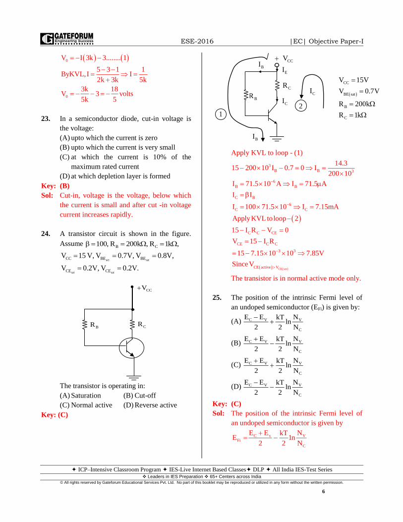
24. A transistor circuit is shown in the figure.
Assume B C100, R 200k , R 1k ,
act sat
sat sat
CC BE BE
CE CE
V 15 V, V 0.7V, V 0.8V,
V 0.2V, V 0.2V.
The transistor is operating in:
(A) Saturation (B) Cut-off
(C) Normal active (D) Reverse active
Key: (C)
Apply KVL to loop - (1)
CE sat
3
B B 3
6
B B
C B
6
C C
C C CE
CE C C
3 3
CE active V
14.315 200 10 I 0.7 0 I
200 10
I 71.5 10 A I 71.5 A
I I
I 100 71.5 10 I 7.15mA
ApplyKVL toloop 2
15 I R V 0
V 15 I R
15 7.15 10 10 7.85V
SinceV
The transistor is in normal active mode only.
25. The position of the intrinsic Fermi level of
an undoped semiconductor (EFi) is given by:
(A) C V V
C
E E NkTln
2 2 N
(B) C V V
C
E E NkTln
2 2 N
(C) C V V
C
E E NkTln
2 2 N
(D) C V V
C
E E NkTln
2 2 N
Key: (C)
Sol: The position of the intrinsic Fermi level of
an undoped semiconductor is given by
C v VFi
C
E E NkTE 1n
2 2 N
CC
BE sat
B
C
V 15V
V 0.7V
R 200k
R 1k
1
CR
CI
EI
BR
BICCV
2
CI
BI
CCV
CRBR
ESE-2016 ESE-2016 |EC| Objective Paper-I
ICP–Intensive Classroom Program IES-Live Internet Based Classes DLP All India IES-Test Series Leaders in IES Preparation 65+ Centers across India
© All rights reserved by Gateforum Educational Services Pvt. Ltd. No part of this booklet may be reproduced or utilized in any form without the written permission.
7
26. The stability factor S in a bipolar junction
transistor is:
(A) B
C
1
dI1
dI
(B) B
C
dI11
1 dI
(C) B
C
dI1 1
dI
(D)
B
C
1
dI1
dI
Key: (A)
Sol: C
CO
IS
I
with EEand V cons tan t
Consider the collector current equation of a
BJT in CE configuration:
C B CO...........I I 1 I 1
Differentiating equation (1) with respect to
IC
COB
C C
II1 1
I I
B
CCO C
C CO B
C
C
CO B
C
I1
II I 1
I 1 I I1
I
I 1S
I I1
I
27. The leakage current in an NPN transistor is
due to the flow of:
(A) Holes from base to emitter
(B) Electrons from collector to base
(C) Holes from collector to base
(D) Minority carriers from emitter to
collector
Key: (C)
Sol: In a BJT, current due to the minority carriers at
collector junction is called leakage current. In
npn transistor, it is the current due to holes of
collector region.
28. In Early effect:
(A) Increase in magnitude of Collector
voltage increases space charge width at
the input junction of a BJT
(B) Increase in magnitude of Emitter-Base
voltage increases space charge width of
output junction of a BJT
(C) Increase in magnitude of Collector
voltage increases space charge width of
output junction of a BJT
(D) Decrease in magnitude of Emitter-Base
voltage increases space charge width of
output junction of a BJT
Key: (C)
Sol: Output junction is C-B junction which is
always Reverse Bias and by increasing the
magnitude of Reverse Bias voltage depletion
layer width at Collector – Base junction
increases.
When the CB junction is reverse biased,
with an increase in reverse bias voltage
potential barrier externals more into the
junction. This is called early effect or base
width modulation.
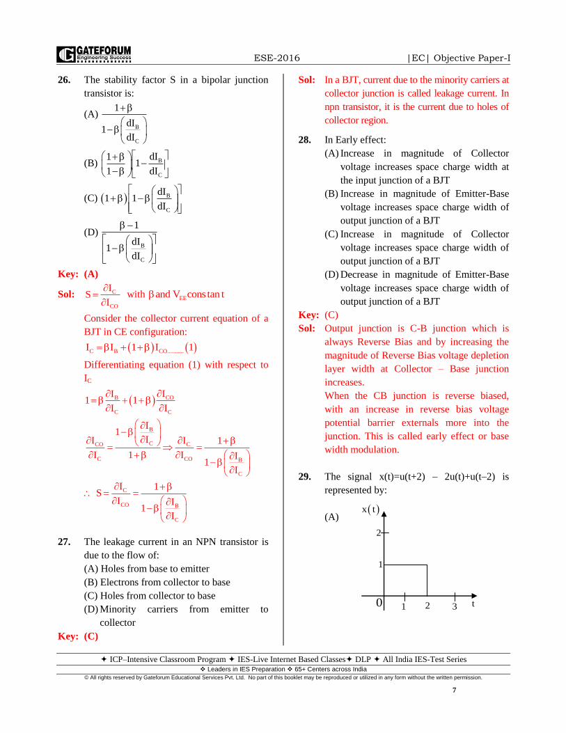
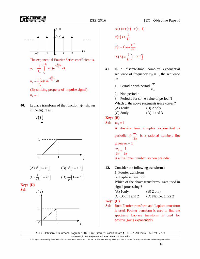
29. The signal x(t)=u(t+2) – 2u(t)+u(t–2) is
represented by:
(A)
x t
2
1
t310 2
ESE-2016 ESE-2016 |EC| Objective Paper-I
ICP–Intensive Classroom Program IES-Live Internet Based Classes DLP All India IES-Test Series Leaders in IES Preparation 65+ Centers across India
© All rights reserved by Gateforum Educational Services Pvt. Ltd. No part of this booklet may be reproduced or utilized in any form without the written permission.
8
(B)
(C)
(D)
Key: (B)
Sol: Number of step signals in any signal is equal
to number of jump discontinuities in it.
x(t) = u(t + 2) –2 u(t) + u(t – 2)
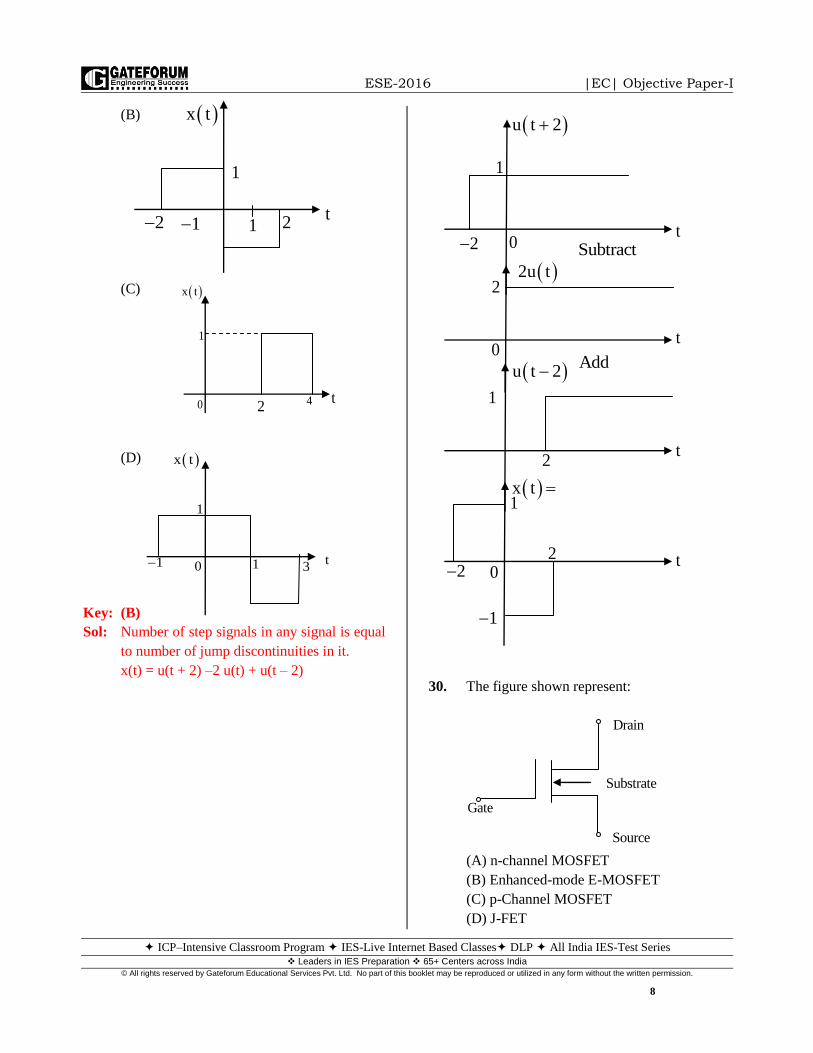
30. The figure shown represent:
(A) n-channel MOSFET
(B) Enhanced-mode E-MOSFET
(C) p-Channel MOSFET
(D) J-FET
t22 1
x t
1
1
x t
1
40 2t
3101 t
x t
1
Substrate
Drain
Source
Gate
t0
1
2u t
2
t
t
t
u t 2
2
0
1
1
2 0
1
2
x t
2
u t 2
Add
Subtract
ESE-2016 ESE-2016 |EC| Objective Paper-I
ICP–Intensive Classroom Program IES-Live Internet Based Classes DLP All India IES-Test Series Leaders in IES Preparation 65+ Centers across India
© All rights reserved by Gateforum Educational Services Pvt. Ltd. No part of this booklet may be reproduced or utilized in any form without the written permission.
9
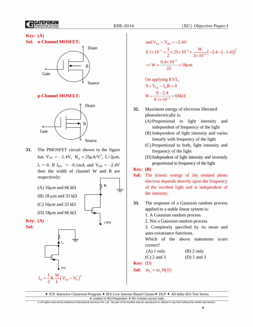
Key: (A)
Sol: n-Channel MOSFET:
p-Channel MOSFET:
31. The PMOSFET circuit shown in the figure
has VTP = –1.4V, '
pK 25A/V2, L=2m,
= 0. If IDS = –0.1mA and VDS = –2.4V
then the width of channel W and R are
respectively:
(A) 16m and 66 k
(B) 18 m and 33 k
(C) 16m and 33 k
(D) 18m and 66 k
Key: (A)
Sol:
2
D GS T
1 WI K V V
2 L
GS DS
23 6
6
3
and V V 2.4V
1 W0.1 10 25 10 2.4 1.4
2 2 10
0.4 10W 16 m
25
On applying KVL,
GS D
3
9 V I R 0
9 2.4R 66k
0.1 10
32. Maximum energy of electrons liberated
photoelectrically is:
(A) Proportional to light intensity and
independent of frequency of the light
(B) Independent of light intensity and varies
linearly with frequency of the light
(C) Proportional to both, light intensity and
frequency of the light
(D) Independent of light intensity and inversely
proportional to frequency of the light
Key: (B)
Sol: The kinetic energy of the emitted photo
electron depends directly upon the frequency
of the incident light and is independent of
the intensity.
33. The response of a Gaussian random process
applied to a stable linear system is:
1. A Gaussian random process
2. Not a Gaussian random process
3. Completely specified by its mean and
auto-covariance functions.
Which of the above statements is/are
correct?
(A) 1 only (B) 2 only
(C) 2 and 3 (D) 1 and 3
Key: (D)
Sol: y xm m H 0
B
Drain
Source
Gate
B
Drain
Source
Gate
9V
R
9V
DI

ESE-2016 ESE-2016 |EC| Objective Paper-I
ICP–Intensive Classroom Program IES-Live Internet Based Classes DLP All India IES-Test Series Leaders in IES Preparation 65+ Centers across India
© All rights reserved by Gateforum Educational Services Pvt. Ltd. No part of this booklet may be reproduced or utilized in any form without the written permission.
10
34. Consider a system, which computes the
‘MEDIAN’ of signal values in a window of
size ‘N’. Such a discrete time system is:
(A) Linear
(B) Non-linear
(C) Sometimes linear
(D) Sometimes non-linear
Key: (B)
Sol: Median is a non linear operator
35. Consider a discrete time system which
satisfies the additivity property, i.e., if the
output for u1[n] is y1[n] and that for u2[n]is
y2[n], then output for u1[n]+ u2[n] is y1[n] +
y2[n]. Such a system is:
(A) Linear
(B) Sometimes linear
(C) Non-linear
(D) Sometimes non-linear
Key: (B&D)
Sol: The system may not satisfy homogeneity
every time. So system may be linear (or)
Non-linear.
36. Consider an ideal low pass filter. Such a
discrete-time system is:
(A) always realizable physically
(B) never realizable physically
(C) a non linear system
(D) a linear, causal system
Key: (B)
Sol: Since the frequency response of an ideal low
pass filter is non-causal it can’t be realized
physically.
37. The result of 0h(2t)* t t (“*” denotes
convolution and “(.)” denotes the Dirac
delta function) is:
(A) 0h 2t 2t (B) 0h(2t 2t)
(C) 0h 2t 2t (D) 0h 2t 2t
Key: (A)
Sol: x(t)* (t) x(t)
0 0
0 0 0
x(t)* (t t ) x(t t )
Shifting property of convolution
h(2 t)* (t t ) h(2(t t )) h(2t 2t )
38. A ray of light incident on a glass slab (of
refractive index 1.5) with an angle, ,4
then
the value of sine of angle of refraction is:
(A) 1
2 (B)
3
2 (C)
2
3 (D) 2
Key: (C)
Sol: r
i
n 1.5
4
From snell’s law
2
1
ri 2 2
t 1 r 1
t
t
t
sin n
sin n
sin / 4 1.5
sin 1
1 2 1sin sin / 4
1.5 3 2
2sin
3
39. The complex exponential power form of
Fourier series of x(t) is:
0
2j .ktT
k
k
x(t) a .e ,
If b
x(t) (t b)
then the value of ak
is:
(A) k1 ( k) (B) k1 ( 1)
(C) 1 (D) 1
Key: (C)
Sol: b
x t t b
ESE-2016 ESE-2016 |EC| Objective Paper-I
ICP–Intensive Classroom Program IES-Live Internet Based Classes DLP All India IES-Test Series Leaders in IES Preparation 65+ Centers across India
© All rights reserved by Gateforum Educational Services Pvt. Ltd. No part of this booklet may be reproduced or utilized in any form without the written permission.
11
The exponential Fourier Series coefficient is,
a 0
0
a
2t Tj ktT
k
0 t
1a x(t)e dt
T
0
21 j ktT
k
0
k
1a (t)e dt
1
(By shifting property of impulse signal)
a 1
40. Laplace transform of the function v(t) shown
in the figure is :
(A) 2 ss 1 e (B) 2 ss 1 e
(C) s
2
11 e
s (D)
s
2
11 e
s
Key: (D)
Sol:
2
s
2
S
2
x t r t r t 1
1r t
S
er t 1
S
1X S 1 e
S
41. In a discrete-time complex exponential
sequence of frequency 0 = 1, the sequence
is:
1. Periodic with period 0
2
2. Non periodic
3. Periodic for some value of period N
Which of the above statements is/are correct?
(A) 1only (B) 2 only
(C) 3only (D) 1 and 3
Key: (B)
Sol: 0 1
A discrete time complex exponential is
periodic if 0
2
is a rational number. But
given 0 = 1
0 1
2 2
is a irrational number, so non periodic
42. Consider the following transforms:
1. Fourier transform
2. Laplace transform
Which of the above transforms is/are used in
signal processing ?
(A) 1only (B) 2 only
(C) Both 1 and 2 (D) Neither 1 nor 2
Key: (C)
Sol: Both Fourier transform and Laplace transform
is used. Fourier transform is used to find the
spectrum, Laplace transform is used for
positive going exponentials.
x(t)
t
t012 1 2
1
v t
0 t1
1
v t
0 t1
ESE-2016 ESE-2016 |EC| Objective Paper-I
ICP–Intensive Classroom Program IES-Live Internet Based Classes DLP All India IES-Test Series Leaders in IES Preparation 65+ Centers across India
© All rights reserved by Gateforum Educational Services Pvt. Ltd. No part of this booklet may be reproduced or utilized in any form without the written permission.
12
43. The varactor diode has a voltage-dependent:
1. Resistance
2. Capacitance
3. Inductance
Which of the above is/are correct?
(A) 1 only (B) 2 only
(C) 3 only (D) 1 and 3
Key: (B)
Sol: A varactor diode is a reverse biased junction
diode whose capacitance can be changed
with the applied reverse bias voltage.
44. The impulse response for the discrete-time
system:
y[n] = 0.24 (x[n]+x[n–1]+x[n–2]+x[n–3]) is
given by
(A) 0 for 0 n 3 and 0.24 otherwise
(B) 0.24 for 0 n 3 and 0 otherwise
(C) 0.24 for n = 0 to n =
(D) 0 for n = 0 to n =
Key: (B)
Sol: y(n) = 0.24 (x[n]+x[n–1]+x[n–2]+x[n–3])
Applying Z-Transform
Y(z) = 0.24 [X(z) + z–1
X(z) +z–2
X(z) + z–3
X(z)]
H(z) = 0.24 [1 +z–1
+ z–2
+z–3
] =Y(z)
X(z)
By using Inverse Z-Transform
h(n) = 0.24 (n) + 0.24 (n–1) + 0.24 (n–2)
+ 0.24(n–3)
h(n) = [0.24,0.24,0.24,0.24]
h(n) = 0.24 ; 0 n 3
0 ; otherwise
45. The product of emitter efficiency () and Base
transport factor (*) for a BJT is equal to:
(A) Small signal current gain
(B) High frequency current gain
(C) Power loss in the BJT
(D) Large-signal current gain
Key: (D)
Sol: For a BJT,
*
Where is large signal current gain.
46. Consider a two-sided discrete-time signal
(neither left sided, nor right sided). The
region of convergence (ROC) of the Z -
transform of the sequence is:
1. All region of z-plane outside a unit circle
(in z-plane)
2. All region of z-plane inside a unit circle
(in z-plane)
3. Ring in z-plane
Which of the above is/are correct?
(A) 1only (B) 2 only
(C) 3 only (D) 1 and 3
Key: (C)
Sol: For a two sided signal ROC is a ring which
is bounded by poles (or) it may not exist.
Thus only statement 3 is to be considered.
47. When is a function f(n) said to be left sided ?
(A) f(n) = 0 for n < 0
(B) f(n) < 0 for n > 0
(C) f(n) = 0 for n > n0
(D) f(n) = for n < n0
(n0 Positive or negative integer)
Key: (C)
Sol: If a sequence is defined as zero for all
positive values of time including zero with
same (or) all negative time sequences then it
is be left sided.
48. Z-transform deals with discrete time systems
for their:
1. Transient behavior
2. Steady-state behavior
Which of the above behaviours is/are
correct?
(A) 1only (B) 2 only
(C) Both 1 and 2 (D) Neither 1 nor 2
Key: (C)
Sol: Solving constant coefficient difference
equations with initial conditions using z-

ESE-2016 ESE-2016 |EC| Objective Paper-I
ICP–Intensive Classroom Program IES-Live Internet Based Classes DLP All India IES-Test Series Leaders in IES Preparation 65+ Centers across India
© All rights reserved by Gateforum Educational Services Pvt. Ltd. No part of this booklet may be reproduced or utilized in any form without the written permission.
13
transform gives transient response as well as
steady state response.
49. The response of a linear, time-invariant
discrete-time system to a unit step input u[n]
is [n]. The system response to a ramp input
n u[n] would be:
(A) [n–1] (B) u[n–1]
(C) n [n–1] (D) n u[n–1]
Key: (B)
Sol: It is given that
x(n) = u(n), y(n) = (n)
By first difference,
u(n)–u(n – 1) = (n)
y(n) = x(n) –x(n – 1)
Now x(n) = nu(n)
y(n) = nu(n)–(n – 1) u (n – 1)
y(n) = n u(n) – n u(n–1) + u(n–1)
y(n) = n (n) + u(n – 1) = 0 + u (n – 1)
y (n) = u(n – 1)
50. Consider a discrete-random variable z
assuming finitely many values. The
cumulative distribution function, Fz(Z) has the
following properties:
1. zF (z)dz 1
2. Fz(z) is non-decreasing with finitely
many jump-discontinuities
3. Fz(z) is negative and non-decreasing
Which of the above properties is/are correct?
(A) 1 only (B) 2 only
(C) 3 only (D) 2 and 3
Key: (B)
51. Consider a random process given by: x(t) =
Acos(2fct+), where A is a Rayleigh
distributed random variable and is
uniformly distributed in [0, 2]. A and are
independent. For any time t, the probability
density function (PDF) of x(t) is:
(A) Gaussian
(B) Rayleigh
(C) Rician
(D) Uniform in [–A, A]
Key: (A)
Sol: The envelope of Gaussian random variable
is Rayleigh and phase is uniform.
52. Poisson’s equation is derived with the
following assumption about the medium.
The medium is:
(A) Non-homogeneous and isotropic
(B) Non-homogeneous and non-isotropic
(C) Homogeneous and non-isotropic
(D) Homogeneous and isotropic
Key: (D)
Sol: From gauss law we know
v
v
.D
D E
. E
If the medium is homogeneous and isotropic
then only E can be taken out.
v
v
2 v
.E
E V
. V
V
53. The state space representation of a linear
time invariant system is:
X(t) AX(t) Bu(t)
Y(t) = CX(t)
What is the transfer function H(s) of the
system?
(A) C (sI – A)–1
B
(B) B (sI – A) –1
C
(C) C (sI – A)B
(D) B (sI – A)C
Key: (A)

ESE-2016 ESE-2016 |EC| Objective Paper-I
ICP–Intensive Classroom Program IES-Live Internet Based Classes DLP All India IES-Test Series Leaders in IES Preparation 65+ Centers across India
© All rights reserved by Gateforum Educational Services Pvt. Ltd. No part of this booklet may be reproduced or utilized in any form without the written permission.
14
54. N
0
k 10 0
1 2x(t) cosk t,
T T
is the combined
trigonometric form of Fourier series for:
(A) Half rectified wave
(B) Saw-tooth wave
(C) Rectangular wave
(D) Impulse train
Key: (D)
Sol: As sine terms are missing in Trignometric
Fourier series expansions it should be an
even signal
a 0 a 0
a a
a 0
a
a 0
a
a 0
a
a 0
a
t T t T
0t t
0 0 0
t T
n 0
0 t
t T
0
0 0t
t T
n 0
0 t
t T
0
0 t
1 1 1a x t dt t dt
T T T
2a x t .cos k t dt
T
2 2t .cos k t dt
T T
2b x t .sin k t dt
T
2t .sin k t dt 0
T
55. A signal xn is given by x0 = 3, x1 =2, x2 = 5,
x3 = 1, x4 = 0, x5 = 1, x6 = 2, x7 = 2, x8 = 4,
where the subscript ‘n’ denotes time. The
peak value of the auto correlation of x[2n-
11] is :
(A) 0 (B) 10 (C) 54 (D) 64
Key: (B)
Sol: x n 3,2,5,1,0,1,2,2,4
x n 11
0,0,0,0,0,0,0,0,0,0,0,3,2,5,1,0,1,2,2,4
y n x 2n 11 0,0,0,0,0,0,2,1,1,2
y(n) correlation y(n) = y(n) * y(–n)
y( n) [2,1,1, 2, 0, 0, 0, 0, 0, 0]
y(n)*y(n) =
[0,0,0,0,0,0,4,4,5,10,5,4,4,0,0,0,0,0,0]
Highest value is ‘10’
56. A system has impulse response h[n] =
cos(n)u[n]. The system is:
(A) Causal and stable
(B) Non causal and stable
(C) Non causal and not stable
(D) Causal and not stable
Key: (D)
Sol: h(n) = cos (n). u(n)
If any signal is multiplied with u[n] it is
causal
n n 0
h n cos n ,
not stable
Since the absolute summation of h[n]
infinite. It is unstable.
t0
t
0T02T 0T02T
2 1 1 2 0 0 0 0 0 0
0 0 0 0 0 0 0 0 0 0 0
0 0 0 0 0 0 0 0 0 0 0
0 0 0 0 0 0 0 0 0 0 0
0 0 0 0 0 0 0 0 0 0 0
0 0 0 0 0 0 0 0 0 0 0
0 0 0 0 0 0 0 0 0 0 0
2 4 2 2 4 0 0 0 0 0 0
1 2 1 1 2 0 0 0 0 0 0
1 2 1 1 2 0 0 0 0 0 0
2 4 2 2 4 0 0 0 0 0 0

ESE-2016 ESE-2016 |EC| Objective Paper-I
ICP–Intensive Classroom Program IES-Live Internet Based Classes DLP All India IES-Test Series Leaders in IES Preparation 65+ Centers across India
© All rights reserved by Gateforum Educational Services Pvt. Ltd. No part of this booklet may be reproduced or utilized in any form without the written permission.
15
57. If the three resistors in a delta network are
all equal in values i.e. RDELTA, then the value
of the resultant resistors in each branch of
the equivalent star network i.e. RSTAR will be
equal to: D DELTA S STARR R ;R R
(A) DELTAR
3 (B) DELTAR
2
(C) DELTA2R (D)
DELTAR
Key: (A)
Sol:
DELTA DELTA DELTASTAR
DELTA DELTA DELTA
R R RR
R R R 3
58. Loop-voltage equations of a passive circuit
are given by:
11 12 13 1 1
21 22 23 2 2
31 32 33 3 3
Z Z Z I V
Z Z Z I V
Z Z Z I V
1. ij jiZ Z ,i, j 1,2,3
2. iiZ 0,i 1,2,3
3. Z 0
Which of the above relations are correct ?
(A) 1 and 2 only (B) 1 and 3 only
(C) 2 and 3 only (D) 1, 2 and 3
Key: (A)
Sol: 1. Zij = Zji , i, j = 1, 2, 3
2. Zii > 0, i=1, 2, 3
When it is passive network it is reciprocal
Zij = Zji
and Zii should greater than 0
Z value should greater than zero
59. A function c(t) satisfies the differential
equation c(t) c(t) (t) For zero initial
condition c(t) can be represented by:
(A) e–t (B) e
t (C) e
tu(t) (D) e
–tu(t)
Where u(t) is a unit step function.
Key: (D)
Sol: c(t) c(t) (t)
Apply time differentiation property of ULT,
t
sC s c 0 C s 1
c 0 0
1C s
S 1
By using inverse laplace transform
c t e .u t
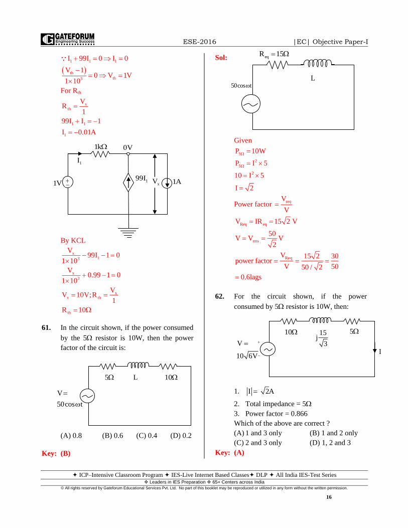
60. For the network shown, Thevenin’s equivalent
voltage source and resistance are, respectively:
(A) 1mV and 10 (B) 1V and 1k
(C) 1mV and 1k (D) 1V and 10
Key: (D)
Sol: For Vth
By KCL
th
13
V 199I 0;
1 10
199I1V
1k
1IA
B
DELTARDELTAR
DELTAR
STARR
STARR
STARR
199I1V
1k
1I
A
B
thV
thV
ESE-2016 ESE-2016 |EC| Objective Paper-I
ICP–Intensive Classroom Program IES-Live Internet Based Classes DLP All India IES-Test Series Leaders in IES Preparation 65+ Centers across India
© All rights reserved by Gateforum Educational Services Pvt. Ltd. No part of this booklet may be reproduced or utilized in any form without the written permission.
16
1 1 1
th
th3
I 99I 0 I 0
V 10 V 1V
1 10
For Rth
xth
1 1
1
VR
1
99I I 1
I 0.01A
By KCL
x13
x
3
xx th
th
V99I 1 0
1 10
V0.99 1 0
1 10
VV 10V;R
1
R 10
61. In the circuit shown, if the power consumed
by the 5 resistor is 10W, then the power
factor of the circuit is:
(A) 0.8 (B) 0.6 (C) 0.4 (D) 0.2
Key: (B)
Sol:
Given
5
2
5
2
P 10W
P I 5
10 I 5
I 2
Power factor reqV
V
Req eq
rms
Req
V IR 15 2 V
50V V V
2
V 15 2 30power factor
V 5050 / 2
0.6lags
62. For the circuit shown, if the power
consumed by 5 resistor is 10W, then:
1. I 2A
2. Total impedance = 5
3. Power factor = 0.866
Which of the above are correct ?
(A) 1 and 3 only (B) 1 and 2 only
(C) 2 and 3 only (D) 1, 2 and 3
Key: (A)
199I1V
1k
1I
0V
1AxV
105
V
50cos t
L
eqR 15
50cos tL
10 5
15j
3V
10 6V
I
ESE-2016 ESE-2016 |EC| Objective Paper-I
ICP–Intensive Classroom Program IES-Live Internet Based Classes DLP All India IES-Test Series Leaders in IES Preparation 65+ Centers across India
© All rights reserved by Gateforum Educational Services Pvt. Ltd. No part of this booklet may be reproduced or utilized in any form without the written permission.
17
Sol:
1. Power consumed by 5 is10W
2I 5 10 I 2Amps
2. Total impedance15
Z 10 5 j13
15Z 15 j
3
30Z 10 3
3
3. eqR eq
V IRPower factorcos
V V
2 10 5 15 2 3cos
210 6 10 6
0.866
63. For a given fixed tree of a network, the
following form an independent set:
1. Branch currents
2. Link voltages
Which of the above is/are correct?
(A) 1 only (B) 2 only
(C) Both 1 and 2 (D) Neither 1 nor 2
Key: (D)
Sol: Branch voltages are related independent of
cut set. Link currents are related independent
of Tieset.
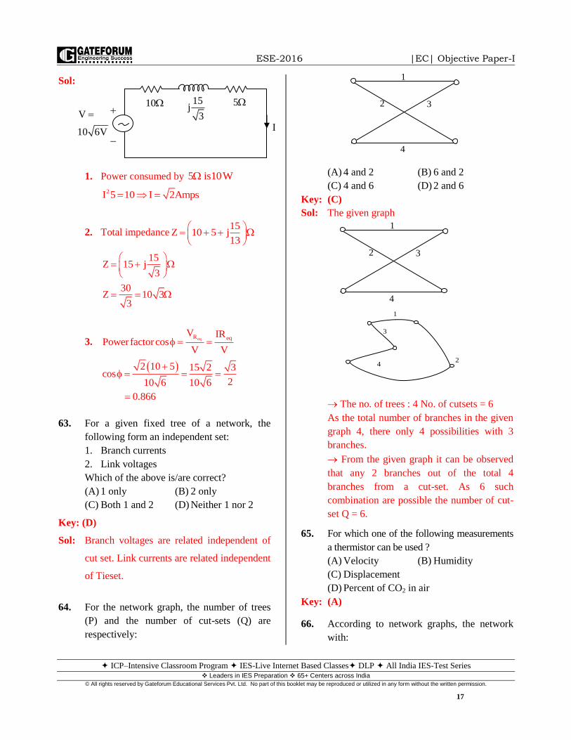
64. For the network graph, the number of trees
(P) and the number of cut-sets (Q) are
respectively:
(A) 4 and 2 (B) 6 and 2
(C) 4 and 6 (D) 2 and 6
Key: (C)
Sol: The given graph
The no. of trees : 4 No. of cutsets = 6
As the total number of branches in the given
graph 4, there only 4 possibilities with 3
branches.
From the given graph it can be observed
that any 2 branches out of the total 4
branches from a cut-set. As 6 such
combination are possible the number of cut-
set Q = 6.
65. For which one of the following measurements
a thermistor can be used ?
(A) Velocity (B) Humidity
(C) Displacement
(D) Percent of CO2 in air
Key: (A)
66. According to network graphs, the network
with:
32
1
4
32
1
4
1
3
42
10 5
15j
3V
10 6V
I

ESE-2016 ESE-2016 |EC| Objective Paper-I
ICP–Intensive Classroom Program IES-Live Internet Based Classes DLP All India IES-Test Series Leaders in IES Preparation 65+ Centers across India
© All rights reserved by Gateforum Educational Services Pvt. Ltd. No part of this booklet may be reproduced or utilized in any form without the written permission.
18
1. Only two odd vertices is traversable
2. No odd vertices is traversable
3. Two or more than two odd vertices are
traversable
Which of the above statements is/are correct?
(A) 1 only (B) 2 only
(C) 3 only (D) 1 and 2
Key: (D)
67. For any lumped network, for any cut sets
and at any instant of time the algebraic sum
of all branch currents traversing the cut-set
branches is always:
(A) One (B) Zero
(C) Infinity
(D) Greater than zero, but less than one
Key: (B)
68. Which one of the following statements
concerning Tellegen’s theorem is correct?
(A) It is useful in determining the effects in
all parts of a linear four-terminal
network
(B) It is applicable for any lumped network
having elements which are linear or
nonlinear, active or passive, time varying
or time-invariant, and may contain
independent or dependent sources
(C) It can be applied to a branch, which is
not coupled to other branches in a
network
(D) It states that the sum of powers taken by all
elements of a circuit within constraints
imposed by KCL and KVL is non-zero
Key: (B)
69. The open circuit input impedance of a 2-port
network is
(A) A
C (B)
B
D (C)
D
C (D)
A
B
Key: (A)
Sol: For T-parameter
1 2 2
1 2 2
V AV BI
I CV DI
2
111
1 I 0
211
2
VZ
I
AV AZ
CV C
70. Consider the following statements:
1. Two identical 2nd order Butterworth LP
filters when connected in cascade will
make a 4th order Butterworth LP filter.
2. A high 2nd order filter will exhibit a
peak if Q exceeds certain value.
3. A band pass filter cannot be of order
one.
4. A network consists of an amplifier of
real gain A and a network in cascade
with each other. The network will
generate sinusoidal oscillations if the
network is a first order LP filter.
Which of the above statements are correct?
(A) 1 and 2 (B) 2 and 3
(C) 3 and 4 (D) 1 and 4
Key: (B)
71. The lowest and the highest critical freque-
ncies of RC driving point admittance are,
respectively:
(A) a zero and a pole
(B) a pole and a zero
(C) a zero and a zero
(D) a pole and a pole
Key: (A)
Sol: The lowest & highest critical frequencies of
RC driving point impedance
For RL impedance and RC Admittance
function the critical frequency nearest to the
ABCD
ESE-2016 ESE-2016 |EC| Objective Paper-I
ICP–Intensive Classroom Program IES-Live Internet Based Classes DLP All India IES-Test Series Leaders in IES Preparation 65+ Centers across India
© All rights reserved by Gateforum Educational Services Pvt. Ltd. No part of this booklet may be reproduced or utilized in any form without the written permission.
19
origin or at the origin must be a zero.
Whereas the critical frequency nearest to
infinity or at infinity must be a pole.
72. The poles and zeros of a voltage function
v(t) are: zero at the origin and simple poles
at –1, –3 and the scale factor is 5. The
contribution of the pole at –3 to v(t) is:
(A) 3t2.5e (B) 3t7.5e
(C) 3t2.5e (D) 3t7.5e
Key: (B)
t 31
5 s 0 5sV s
s 1 s 3 s 1 s 3
5 2 15 2
s 1 s 3
5 15V t e .u t e .u t
2 2
The contribution of the pole at ‘–3’ to v(t) is
7.5e–3t
u(t)
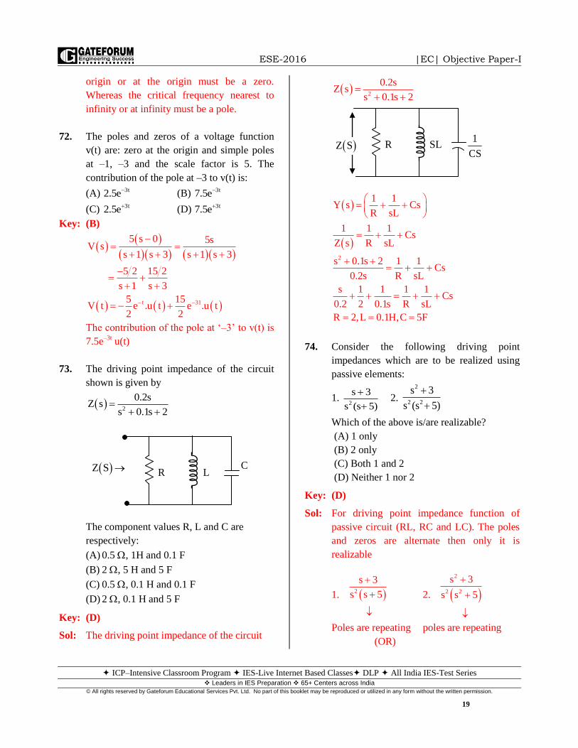
73. The driving point impedance of the circuit
shown is given by
2
0.2sZ s
s 0.1s 2
The component values R, L and C are
respectively:
(A) 0.5 , 1H and 0.1 F
(B) 2 , 5 H and 5 F
(C) 0.5 , 0.1 H and 0.1 F
(D) 2 , 0.1 H and 5 F
Key: (D)
Sol: The driving point impedance of the circuit
2
0.2sZ s
s 0.1s 2
2
1 1Y s Cs
R sL
1 1 1Cs
Z s R sL
s 0.1s 2 1 1Cs
0.2s R sL
s 1 1 1 1Cs
0.2 2 0.1s R sL
R 2,L 0.1H,C 5F
74. Consider the following driving point
impedances which are to be realized using
passive elements:
1. 2
s 3
s (s 5)
2.
2
2 2
s 3
s (s 5)
Which of the above is/are realizable?
(A) 1 only
(B) 2 only
(C) Both 1 and 2
(D) Neither 1 nor 2
Key: (D)
Sol: For driving point impedance function of
passive circuit (RL, RC and LC). The poles
and zeros are alternate then only it is
realizable
1. 2
s 3
s s 5
2.
2
2 2
s 3
s s 5
Poles are repeating poles are repeating
(OR)
CLR Z S
1
CSSLR Z S

ESE-2016 ESE-2016 |EC| Objective Paper-I
ICP–Intensive Classroom Program IES-Live Internet Based Classes DLP All India IES-Test Series Leaders in IES Preparation 65+ Centers across India
© All rights reserved by Gateforum Educational Services Pvt. Ltd. No part of this booklet may be reproduced or utilized in any form without the written permission.
20
Both cannot be realized as the difference
between highest degree of numerator and
denominator polynomial is greater than one.
75. A reactance function in the first Foster form
has poles at = 0 and = . The black-box
(B.B) in the network contains:
(A) An inductor
(B) A capacitor
(C) A parallel L – C circuit
(D) A series L – C circuit
Key: (B)
Sol: A reactance function in the first Foster form
has poles at = 0 and =
pole at origin It is capacitor in series.
Black Box should contains only capacitor.
76. Consider the following statements:
1. The magnetic field at the centre of a
circular coil of a wire carrying current is
inversely proportional to the radius of
the coil
2. Lifting power of a magnet is proportional to
square of magnetic flux density
3. A static electric field is conservative
(irrotational).
4. If the divergence of a vector ‘A’ is zero,
then vector ‘A’ can be expressed as Curl
of a vector F
Which of the above statements are correct?
(A) 1, 2 and 3 only (B) 3 and 4 only
(C) 1, 2 and 4 only (D) 1, 2, 3 and 4
Key: (D)
Sol: 1. The magnetic field at the centre at
circular coil is given by
1
H2a
a radius
2. Lifting force 2B s
F2
2F B
3. E 0
E Static electric field
Static electric field is irrotational
4. .A 0
A F
Any solenoidal vector can be expressed
as curl of some other vector.
77. Consider the following:
1. Electric current flowing in a conducting
wire
2. A moving charged belt
3. An electron beam in a cathode ray tube
4. Electron movement in a vacuum tube
Which of the above are examples of
convection current?
(A) 2, 3 and 4 only
(B) 1, 2 and 4 only
(C) 1 and 3 only
(D) 1, 2, 3 and 4
Key: (A)
78. Consider the following sources:
1. A permanent magnet
CB.B
L
CB.B
L
ESE-2016 ESE-2016 |EC| Objective Paper-I
ICP–Intensive Classroom Program IES-Live Internet Based Classes DLP All India IES-Test Series Leaders in IES Preparation 65+ Centers across India
© All rights reserved by Gateforum Educational Services Pvt. Ltd. No part of this booklet may be reproduced or utilized in any form without the written permission.
21
2. A charged disc rotating at uniform speed
3. An accelerated charge
4. An electric field which changes linearly
with time
Which of the above are the sources of steady
magnetic field?
(A) 1, 2 and 3 only
(B) 3 and 4 only
(C) 1, 2 and 4 only
(D) 1, 2, 3 and 4
Key: (C)
Sol: Sources of steady magnetic field are
1. permanent magnet
2. a charged disc rotating at uniform speed
4. an electric field which changes linearly
with time but change with acceleration
provides time varying magnetic field.
79. A charge Q is enclosed by a Gaussian
spherical surface of radius R. If R is doubled
then the outward flux is
(A) Doubled
(B) Increased four times
(C) Reduced to a quarter
(D) Remains unaltered
Key: (D)
Sol: Flux does not changes with radius. Since the
amount of charge enclosed does not change
with respect to radius.
80. Divergence of a vector div D in the cylindrical
coordinate system is
(A) z
D D1 1(D )
p z
(B)
zD (ZD )1 1 1
( D )z z
(C) zD D1 1
( D )z
(D) zD D D
z
Key: (C)
Sol: zD D1 1
.D Dz
It is a standard formula.
81. What is the value of work required to move
a +8 nC charge from infinity to a point P
which is at 2m distance from a point charge
Q = + 5 C ?
(A) 180 J (B) 180 nJ
(C) 18 J (D) 18 nJ
Key: (A)
Sol: 21
Q1W Q V V
4 r
9 9 6
1 2Q Q1 9 10 8 10 5 10W
4 r 2
W 180 J
82. An electrostatic force between two point
charges increases when they are:
(A) More apart and dielectric constant of the
medium between them decreases
(B) Less apart and dielectric constant of the
medium between them decreases
(C) More apart and dielectric constant of the
medium between them increases
(D) Less apart and dielectric constant of the
medium between them increases
Key: (B)
Sol: 1 2
2
1 2
2
Q Q1F
4 R
Q QF
R
83. A plane Y = 2 carries infinite sheet of charge
6 nC/m2. If medium is free space then force
on a point charge of 10 mC located at the
origin is:
(A) y1080 a N (B) y108 a N
(C) y10.8 a N (D) y1.08 a N

ESE-2016 ESE-2016 |EC| Objective Paper-I
ICP–Intensive Classroom Program IES-Live Internet Based Classes DLP All India IES-Test Series Leaders in IES Preparation 65+ Centers across India
© All rights reserved by Gateforum Educational Services Pvt. Ltd. No part of this booklet may be reproduced or utilized in any form without the written permission.
22
Key: (D)
Sol: Since force is inversely proportional to E, R.
so, when E, R decreases F increases.
Plane y = 2
9
sn y
9
6 10E a a
122 10
36
y
3y
3y
y
E 108 a
F QE
10 10 108 a
1080 a 10
F 1.80 a N
84. The potential at the centroid of an equilateral
triangle of side r 3 due to three equal positive
point charges each of value q and placed at the
vertices of the triangle would be
(A) 0
q
2 r (B)
0
3q
8 r
(C) 0
3q
4 r (D) zero
Key: (C)
Sol:
1 2 3V V V V
1 q 1 q 1 q
4 r 4 r 4 r
3qv
4 r
85. The point form of the relation connecting
vector magnetic potential A and current
density J is
(A) D
A Jt
(B) 0JA dv
4 R
(C) 2
0A J (D) A J
t
Key: (C)
Sol: 2
0A J
Poisson’s equation in the magnetic field
86. In the region Z<0, r1 2,
1 x y zE 3a 4a 2a V / m.
For region Z >0. where r2 26.5, E is :
(A) x y z
6.53a 4a a V / m
4
(B) x y z
43a 4a a V / m
6.5
(C) x y z
6.53a 4a a V / m
4
(D) x y z
43a 4a a V / m
6.5
Key: (D)
Sol: x y z1E 3a 4a 2a
a y1t
y1n
1x y2 1n
2
x y z2
E 3a 4a
E 2a
E 3a 4a E
4E 3a 4a a
6.5
87. Consider the following statements regarding
a conductor and free space boundary:
1. No charge and no electric field can exist
at any point within the interior of a
conductor
2. Charge may appear on the surface of a
conductor
Which of the above statements are correct?
(A) 1 only (B) 2 only
(C) Both 1 and 2 (D) Neither 1 nor 2
q
r 3,0
r 3 3r,
2 2
0,0
r 3 r,
2 2

ESE-2016 ESE-2016 |EC| Objective Paper-I
ICP–Intensive Classroom Program IES-Live Internet Based Classes DLP All India IES-Test Series Leaders in IES Preparation 65+ Centers across India
© All rights reserved by Gateforum Educational Services Pvt. Ltd. No part of this booklet may be reproduced or utilized in any form without the written permission.
23
Key: (C)
Sol:
Because of repulsive force between electrons,
they exist on surface.
88. A sphere of homogeneous linear dielectric
material of dielectric constant 1 is placed in a
uniform electric field E0, then the electric field
E that exists inside the sphere is
(A) Uniform and E E0
(B) Uniform and E E0
(C) Varies but E < E0 always
(D) Varies but E > E0 always
Key: (C)
Sol:
0
0 0 r
1 1 1E E E
Electric field inside the sphere,
v
r 0
rE
3
1;E E
89. Which of the following Maxwell’s equation
represents Ampere’s law with correction
made by Maxwell?
(A) 0
.E
(B) .B 0
(C) B
Et
(D) 0 0 0
EB J
t
Key: (D)
Sol: D
H Jt
B EJ
t
EB J
t
90. Precision is composed of two characteristics,
one is the number of significant figures to
which a measurement may be made, the
other is
(A) Conformity (B) Meter error
(C) Inertia effects (D) Noise
Key: (A)
91. If Phasors 1 2P 3 j4 and P 6 j8, then
1 2P P is
(A) 5 (B) 53 (C) 73 (D) 153
Key: (D)
Sol: If phasers 1 2P 3 j4 & P 6 j8
Then
1 2
1 2
P P 3 j4 6 j8 3 j12
P P 9 144 153
92. A plane wave in free space has a magnetic
field intensity of 0.2 A/m in the Y-direction.
The wave is propagating in the Z-direction
with a frequency of 3 GHz. The wavelength
and amplitude of the electric field intensity
are, respectively
(A) 0.05 m, and 75 V/m
(B) 0.10 m and 75 V/m
(C) 0.05 m and 150 V/m
(D) 0.10 m and 150 V/m
Key: (B)
Sol: 0H 0.2
8
9
f 3GHz
V 3 100.1
f 3 10
0 sphere
0E
r 1
r
V
E 0
0
Inside Conductor
ESE-2016 ESE-2016 |EC| Objective Paper-I
ICP–Intensive Classroom Program IES-Live Internet Based Classes DLP All India IES-Test Series Leaders in IES Preparation 65+ Centers across India
© All rights reserved by Gateforum Educational Services Pvt. Ltd. No part of this booklet may be reproduced or utilized in any form without the written permission.
24
0
0
0
0
E120
H
E 0.2 377
E 75.4
93. For energy propagation in a lossless
transmission line, the characteristic impedance
of the line is expressed in ohm as below
(where notations have usual meanings).
(A) LC (B) L
C
(C) C
L (D)
R j L
G j L
Key: (B)
Sol: 0
LZ
C
94. A quarter wave-length transformer is used to
match a load of 200 to a line with input
impedance of 50. The characteristic
impedance of the transformer would be
(A) 40 (B) 100
(C) 400 (D) 1000
Key: (B)
Sol: QWT L 0Z Z Z 200 50 100
95. For a lossless transmission line
L = 0.35H/m, C = 90 pF/m and
frequency = 500 MHz.
Then the magnitude of propagation constant
is
(A) 14.48 (B) 17.63 (C) 19.59 (D) 21.20
Key: (B)
Sol: For lossless transmission line
6 12 6
LC
2 500 10 90 10 0.35 10
17.63
96. If an antenna has a main beam with both
half-power beam widths equal to 20, its
directivity (D) is nearly
(A) 90.6 (B) 102.5
(C) 205 (D) 226
Key: (A)
Sol: If a major lobe and any minor lobes of very
low intensity (minor lobes are ignore) are
present then the directivity is approximately
equal to
0
HP HP
41253 41253D
400
D 103.13
97. An instrument always extracts some energy
from the measured medium. Thus the
measured quantity is always disturbed by the
act of measurement, which makes a perfect
measurement theoretically impossible and it
is due to
(A) Skin-effect
(B) Inductive effect
(C) Loading effect
(D) Lorenz effect
Key: (C)
98. The characteristic impedance 0 of a free
space is
(A) 0
0
(B) 0
0
(C) 0 0 (D)
0 0
Key: (B)
Sol: 00
0
99. A1
32
digit voltmeter has an accuracy
specification of 0.5% of reading one
digit. What is the possible error in volts
when the instrument displays 2.00V on the
10 V scale?
(A) 0.03 V (B) 0.02V
(C) 0.01 V (D) 0.005 V

ESE-2016 ESE-2016 |EC| Objective Paper-I
ICP–Intensive Classroom Program IES-Live Internet Based Classes DLP All India IES-Test Series Leaders in IES Preparation 65+ Centers across India
© All rights reserved by Gateforum Educational Services Pvt. Ltd. No part of this booklet may be reproduced or utilized in any form without the written permission.
25
Key: (B)
Sol:
0.5error 2V 1count
100
0.01V 00.01V
0.01V 0.01V 0.02V
100. A megger is an instrument used for measuring
(A) Very high voltages
(B) Very low voltages
(C) Very high resistances
(D) Very low resistances
Key: (C)
101. The values of capacitance and inductance
used in the series LCR circuit are 160 pF and
160 H with the inherent tolerance – 10% in
each. Then, the resonance frequency of the
circuit is in the range of
(A) 0.8 MHz to 1.2 MHz
(B) 0.9 MHz to 1.0 MHz
(C) 0.8 MHz to 1.0 MHz
(D) 0.9 MHz to 1.2 MHz
Key: (B)
102. Dynamic characteristics of instruments leading
to variations during measurement are
1. Speed of response
2. Fidelity
3. Dynamic error
Which of the above are correct?
(A) 1 and 2 only (B) 1 and 3 only
(C) 2 and 3 only (D) 1, 2 and 3
Key: (A)
103. The reliability of an instrument refers to
(A) Degree to which repeatability continues
to remain within specified limits
(B) The extent to which the characteristics
remain linear
(C) Accuracy of the instrument
(D) Sensitivity of the instrument
Key: (A)
104. AC Voltmeters use diodes with
(A) High forward current and low reverse
current ratings
(B) Low forward current and low reverse
current rating
(C) Low forward current and high reverse
current ratings
(D) High forward currents and high reverse
current ratings
Key: (A)
105. The bridge circuit shown can be used to
measure unknown lossy capacitor CX with
resistance RX. At balance.
(A) 1 1X 2 x 3
3 2
C RR R and C C
C R
(B) 3 2X 2 x 3
1 1
C RR R and C C
C R
(C) 1 1X 2 x 2
2 1
R CR R and C R
C R
(D) X 2 x 3R R and C C
Where R1, R2, C1 and C3 can be assumed
ideal components
Key: (A)
Sol: 1 1 2 2 3
1 3
4 x
x
j jZ R || ; Z R ; Z ;
C C
1Z R j
C
1C
2R
3C xR
xC
G
1R

ESE-2016 ESE-2016 |EC| Objective Paper-I
ICP–Intensive Classroom Program IES-Live Internet Based Classes DLP All India IES-Test Series Leaders in IES Preparation 65+ Centers across India
© All rights reserved by Gateforum Educational Services Pvt. Ltd. No part of this booklet may be reproduced or utilized in any form without the written permission.
26
1
1 11
1 1
1
1
jR
C jRZ
R C j1R j
C
1 11
1
1 1 1 1
2
1 1 1
2 2 2
1 1
On rationalising,we get
R C jjRZ
R C j R C j
R j R C
R C 1
1 4 2 3Bridgebalancecondition,Z Z Z Z
2
32 34 2
1 1 11
2 2 2
1 1
jR
CZ ZZ
R j R CZ
R C 1
2 2 2
1 1 2
3
2
1 1 1
j1 R C .R
C
R j R C
Onrationalising,weget
2 2 2
4 2 1 1Z R 1 R C
2
1 1 1
3
2 2 4 2
1 1 1
jR j R C
C
R R C
2 2 2
2 1 1
x 2 2 2 2x 1 1 1
2
1 1 1
3 3
R 1 R C1R j
C R 1 R C
R C Rj
C C
2 1x
3
R CR
C
2 1
2
x 1 3
R R1j j
C R C
1
3
2
1j
R. C
R
2
2 1 1x 2
1 3
R R CR
R C
1x 3
2
1x 3
2
RC . C
R
RC .C
R
106. Inductance of a coil having Q value in the
range of (1< Q< 10), can be measured by
using
(A) Hay’s bridge
(B) De Sauty’s bridge
(C) Maxwell’s bridge
(D) Carry Foster’s bridge
Key: (C)
107. The instrument servomechanism is actually
an instrument system made of components,
which are
(A) Exclusively passive transducers
(B) Exclusively active transducers
(C) Combination of passive transducers and
active transducers
(D) Exclusively primary sensing elements
Key: (C)
108. The scale of an electrodynamometer usually
reads the
(A) Average value of the ac
(B) Mean value of the ac
(C) Effective value of the ac
(D) Squared value of the ac
Key: (B)
ESE-2016 ESE-2016 |EC| Objective Paper-I
ICP–Intensive Classroom Program IES-Live Internet Based Classes DLP All India IES-Test Series Leaders in IES Preparation 65+ Centers across India
© All rights reserved by Gateforum Educational Services Pvt. Ltd. No part of this booklet may be reproduced or utilized in any form without the written permission.
27
109. The resolution of an indicating instrument
can be defined as
1. Variation in the meter reading for the
same applied input
2. Detectable change in the deflection due
to smallest change in the applied input
3. Detectable change in the output due to
drifting of pointer
Which of the above statements are correct?
(A) 1 only (B) 2 only
(C) 3 only (D) 1 and 3
Key: (B)
110. The expected voltage across a resistor is 100
V. However, the voltmeter reads a value of
97 V. The relative error is
(A) 0.97 (B) 0.03 (C) 0.07 (D) 3.00
Key: (B)
Sol: The relative error r
m tr
t
A A 97 1000.03
A 100
111. While measuring the phase difference between
the signals v1(t) = 10 sin t and v2(t) = 10 sin
(t + ), the Lissajous pattern observed on
CRO is a circle. The value of is
(A) 2 (B) (C) 2
(D)
4
Key: (C)
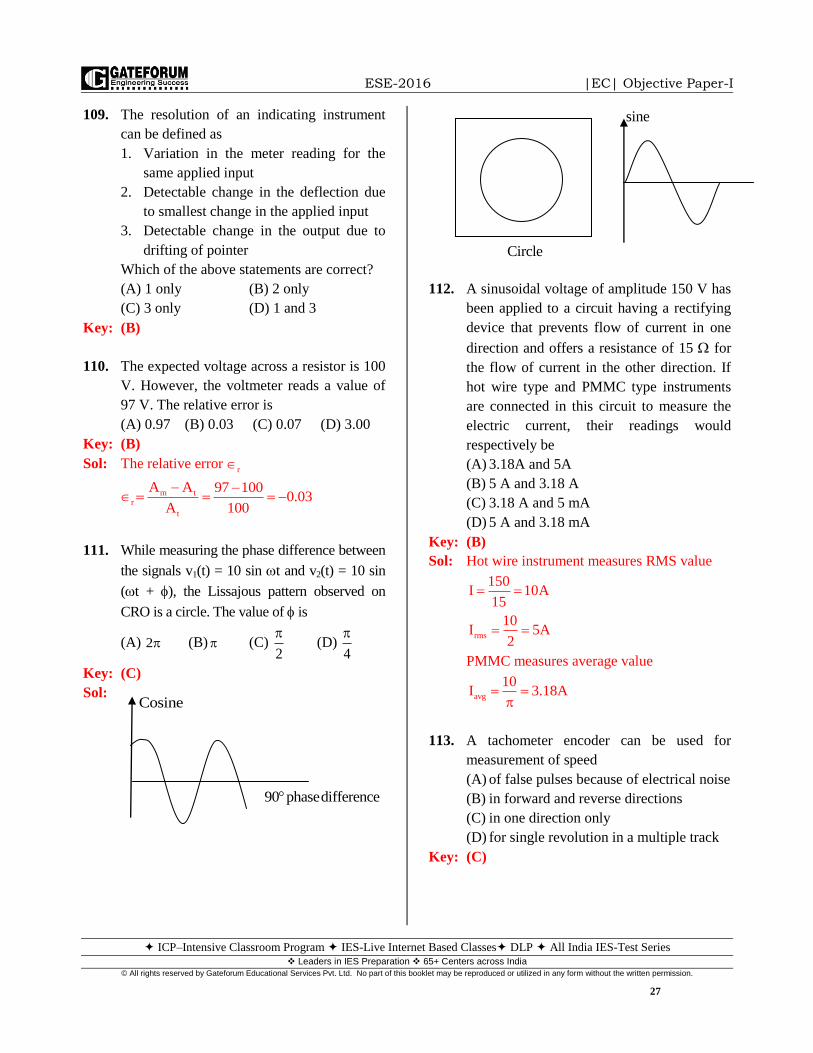
Sol:
112. A sinusoidal voltage of amplitude 150 V has
been applied to a circuit having a rectifying
device that prevents flow of current in one
direction and offers a resistance of 15 for
the flow of current in the other direction. If
hot wire type and PMMC type instruments
are connected in this circuit to measure the
electric current, their readings would
respectively be
(A) 3.18A and 5A
(B) 5 A and 3.18 A
(C) 3.18 A and 5 mA
(D) 5 A and 3.18 mA
Key: (B)
Sol: Hot wire instrument measures RMS value
rms
150I 10A
15
10I 5A
2
PMMC measures average value
avg
10I 3.18A
113. A tachometer encoder can be used for
measurement of speed
(A) of false pulses because of electrical noise
(B) in forward and reverse directions
(C) in one direction only
(D) for single revolution in a multiple track
Key: (C)
Cosine
90 phasedifference
Circle
sine
ESE-2016 ESE-2016 |EC| Objective Paper-I
ICP–Intensive Classroom Program IES-Live Internet Based Classes DLP All India IES-Test Series Leaders in IES Preparation 65+ Centers across India
© All rights reserved by Gateforum Educational Services Pvt. Ltd. No part of this booklet may be reproduced or utilized in any form without the written permission.
28
114. A rotameter works on the principle of variable
(A) Pressure (B) Length
(C) Area (D) Resistance
Key: (C)
115. An input voltage required to deflect a beam
through 3cm in a Cathode Ray Tube having
an anode voltage of 1000V and parallel
deflecting plates 1 cm long and 0.5 cm apart,
when screen is 30 cm from the center of the
plates is
(A) 300 V (B) 200 V
(C) 100 V (D) 75 V
Key: (C)
Sol: d
a
ad
LVD
2dV
D 2 d VV 100V
L
116. A 6-bit ADC has a maximum precision
supply voltage of 20 V. What are the voltage
changes for each LSB present and voltage to
be presented by (100110), respectively ?
(A) 0.317V and 12.06 V
(B) 3.17 V and 12.06 V
(C) 0.317 V and 1.206 V
(D) 3.17 V and 1.206 V
Key: (A)
Sol: A transducer can be anything which converts
one form of energy to another. Piezoelectric
material is one kind. We apply force or
pressure on this material it converts voltage
and this voltage is function of force or
pressure applied to it. The electric voltage
produced by piezoelectric transducer can be
easily measured by voltage measuring
instruments, which can be used to measure
stress or forces. The physical quantity like
mechanical stress or force cannot be
measured directly. Therefore piezoelectric
transducer can be used.
117. Which of the following transducers measure
the pressure by producing emf as a function
of its deformation?
(A) Photoelectric transducer
(B) Capacitive transducer
(C) Inductive transducer
(D) Piezoelectric transducer
Key: (D)
118. Maxwell’s bridge measure an unknown
inductance in terms of
(A) Known inductance
(B) Known capacitance
(C) Known resistance
(D) Q of the coil
Key: (B)
119. Strain gauges are constructed with Germanium
chips because Germanium:
(A) has a strong Hall Effect
(B) is crystalline in nature
(C) can be doped
(D) has piezo-electric property
Key: (C)
120. The advantages of an LVDT is/are
1. Linearity
2. Infinite resolution
3. Low Hysteresis
Which of the above advantages is/are
correct?
(A) 1 only (B) 2 only
(C) 3 only (D) 1, 2 and 3
Key: (D)