nyquist rate d/a converters (12.1-12.4)
TRANSCRIPT

3/2/2010
1
Nyquist Rate D/A Converters (12.1-12.4)Tuesday 2nd of March, 2010, 9:15-11:00
Snorre Aunet, [email protected] Group, Dept. of Informatics
Office 3432
Last time – and today, Tuesday 2nd of March:Last time:
10.3 First-order filters10.4 Biquad filters (high-Q)10.5 Charge injection10 7 C l t d d bl li t h i10.7 Correlated double sampling techniques11.1 Ideal D/A converter11.2 Ideal A/D converter11.3 quantization noise11.4 signed codesToday:11.5 Performance Limitations12.1 Decoder-based converters12.2 Binary-scaled converters12.3 Thermometer-code converters12.4 Hybrid converters10:55 : 5 minute survey by ”Micro”
3/2/2010
2
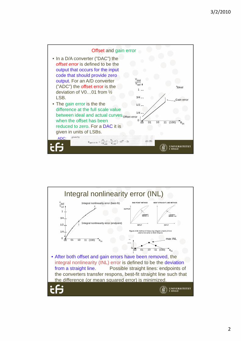
Offset and gain error
Vout
• In a D/A converter (”DAC”) the offset error is defined to be the output that occurs for the input code that should provide zero output For an A/D converter
1
1/2
1/4
3/4
outVref-------------
Ideal
Gain error
Offset error
output. For an A/D converter (”ADC”) the offset error is the deviation of V0…01 from ½ LSB.
• The gain error is the the difference at the full scale value between ideal and actual curves
0100 10 110
(100) Bin
Offset error
when the offset has been reduced to zero. For a DAC it is given in units of LSBs.ADC:
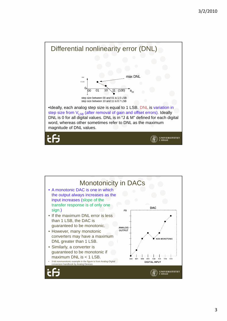
Integral nonlinearity error (INL)
1
3/4
VoutVref-------------
Integral nonlinearity error (endpoint)
Integral nonlinearity error (best-fit)
0100 10 110
1/2
1/4
(100) Bin
Integral nonlinearity error (endpoint)
0100 10 110
(100) Bin
INL
0.5LSB
max INL
• After both offset and gain errors have been removed, the integral nonlinearity (INL) error is defined to be the deviation from a straight line. Possible straight lines: endpoints of the converters transfer respons, best-fit straight line such that the difference (or mean squared error) is minimized.
3/2/2010
3
Differential nonlinearity error (DNL)
max DNL
0100 10 110
(100) Bin
DNL
0.5LSB
max DNL
step size between 00 and 01 is 1.5 LSBstep size between 10 and 11 is 0.7 LSB
•Ideally, each analog step size is equal to 1 LSB. DNL is variation in step size from VLSB (after removal of gain and offset errors). Ideally DNL is 0 for all digital values. DNL is in “J & M” defined for each digital word, whereas other sometimes refer to DNL as the maximum magnitude of DNL values.
Monotonicity in DACs• A monotonic DAC is one in which
the output always increases as the input increases (slope of the transfer response is of only one sign )sign.)
• If the maximum DNL error is less than 1 LSB, the DAC is guaranteed to be monotonic.
• However, many monotonic converters may have a maximum DNL greater than 1 LSB.
• Similarly, a converter is guaranteed to be monotonic if maximum DNL is < 1 LSB.
• 3-bit nonmonotonic example in the figure is from Analog-Digital conversion handbook by Analog Devices

3/2/2010
4
D/A (DAC) settling time and sampling rate• In a DAC the settling time is
defined as the time it takes for the converter to settle within some specified amount of thesome specified amount of the final value (usually 0.5 LSB).
• The sampling rate is the rate at which samples can be continously converted and is typically the inverse of the settling time.g
• Different combinations of input vectors give different settling times. Picture from ”High-speed data converters fully integrated in CMOS”,
dissertation for the dr. scient. degree by Leif Hanssen, Ifi, UiO, 1990.
Nyquist Rate D/A Converters• 12.1 Decoder-based converters
resistor string conv.
folded resistor string conv.multiple R-string converters
• 12.2 Binary-Scaled convertersbinary-weighted resistor convertersreduced resistance-ratio laddersR-2R-based converterscharge-redistribution switched-capacitor conv.current-mode conv.
• 12.3 Thermometer-code convertersthermometer-code current-mode D/A converters
single-supply positive-output converterssingle supply positive output convertersdynamically matched current sources
• 12.4 Hybrid convertersresistor-capacitor hybrid converters
segmented converters

3/2/2010
5
Some systems exploiting data converters, ”Allen & Holberg”
Ideal D/A converter
VD/ABin
Vref
Vout
b1
b2
bN
Bin b121– b22
2– bN2N–
+ + +=
Vout Vref b121– b22
2– bN2N–
+ + + =

3/2/2010
6
Ideal D/A converter
1
VoutVref-------------
2-bit DAC
0100 10 110
1/2
1/4
3/4
(100)
VLSBVref
----------------14--- 1 LSB= =
Bin
VLSBVref
2N
---------- 1 LSB 1
2N
------=
12.1 Decoder-Based Converters• Creates 2N reference signals and passes the appropriate
signal to the output, depending on the digital input word.• The switching network produces one, and only one, low
impedance path between the resistor string and the input of p p g pthe buffer
• Relatively compact switches if n-channel devices are used instead of transmission gates.
Voutb
1b
2
b2
b3
b3
b3
b3
bN
Vref
b1
b2
b2b
3
b3
b3
b3
2N
Resistors
3-bit

3/2/2010
7
Resistor String Converters (12.1)
• Only one path between resistor string and D/A-output
• Guaranteed monotonicity, provided that the voltage follower b
2
b3
b3
Vref
p gdoes not have too large offset
• Compact design when using only n-transistors (no contacts)
• Polysilicon resistors may give resolution up to 10 bit
• Delay through switch network is the major speed limitation of the
Voutb
1b
2
b2
b3
b3
b3
b3
b3
2N
Resistors
circuit• 2N resistors are required (when
only one resistor string is included )
b1
b2b
3
3-bit
Resistor String Converters (12.1) • High-speed implementation
(when compared to the previous one), due to maximum of one switch in series
V r ef
• Less resistance through switches• The switches are controlled by
digital logic• More area for the decoder
compared to the previous DAC• Larger capacitance on the buffer
input, due to the 2N transistors connected to it
2N
R e si st o rs
r ef
b 1
b 2
b 3
3 to
1 o
f 8
deco
der
• Pipelining may be applied for “moderate speed”
• 2N resistors are requiredV o u t
3-b it

3/2/2010
8
Estimating the time constant for n resistors and capacitors in series (ex. 12.2)
Folded Resistor-String Converters 12.1• Reduzing size of digital circuitry and capacitive
loading• 2N resistors are required• b1b2 : Most significant bits in the 4 bit case
(selects one single word line.)
St t i il t h t b f d i di it l• Structure similar to what can be found in digital memories.
• OBS! NMOS switches here• Number of transistor junctions connected to the
output line is now 2 SQRT ( 2N ), instead of 2N
• 4 bit case: 8 instead of 16• 8 bit case: 32 instead of 256• 10 bit case: 64 instead of 1024
V re f
b 1
b 2
2 to
1 o
f 4
dec
oder
word lines
bit
lin
es
• 10 bit case: 64 instead of 1024• When a word line goes high, alle the bit
lines must be pulled to new levels, limiting speed (no increase equal to the ratio ( [2 SQRT ( 2N )] / 2N )b3 b 4
2 to 1 of 4 decoder
V o ut
4-bit
3/2/2010
9
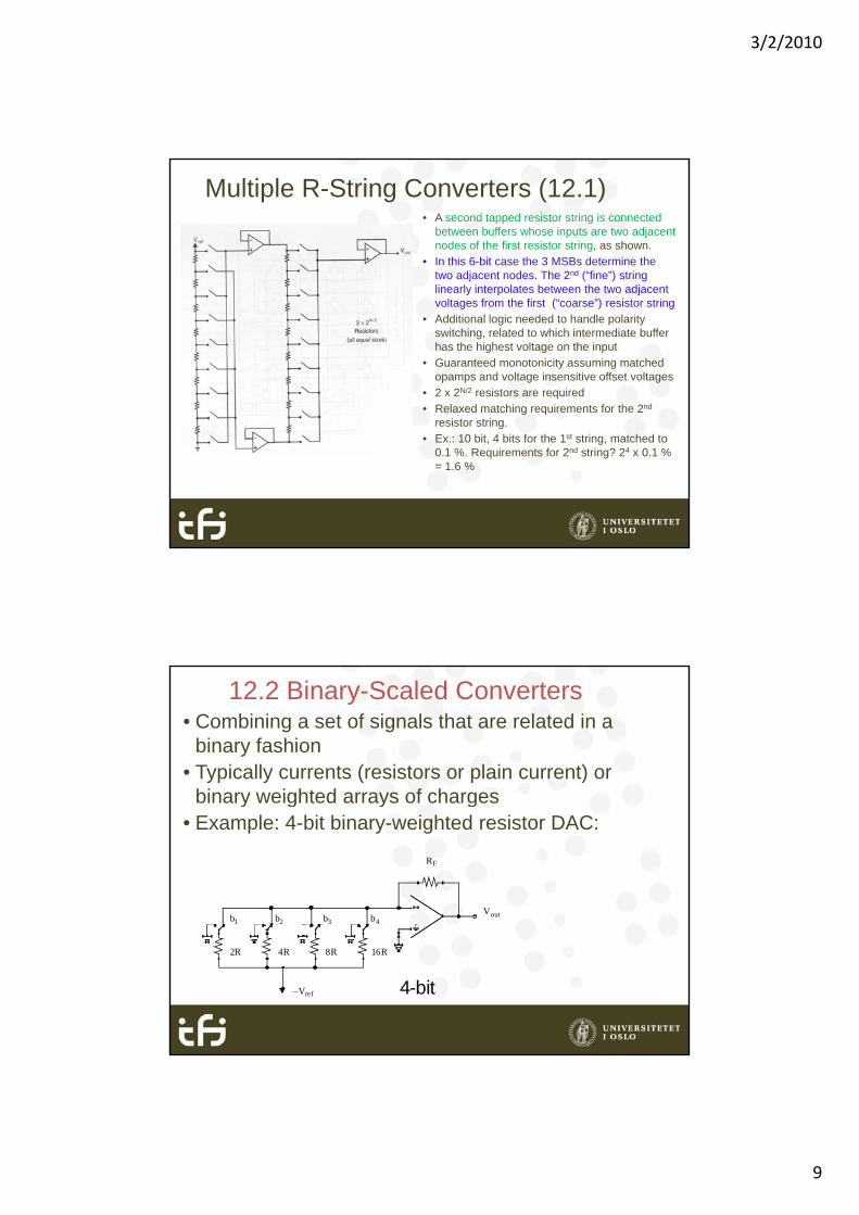
Multiple R-String Converters (12.1)• A second tapped resistor string is connected
between buffers whose inputs are two adjacent nodes of the first resistor string, as shown.
• In this 6-bit case the 3 MSBs determine the two adjacent nodes. The 2nd (“fine”) string linearly interpolates between the two adjacentlinearly interpolates between the two adjacent voltages from the first (“coarse”) resistor string
• Additional logic needed to handle polarity switching, related to which intermediate buffer has the highest voltage on the input
• Guaranteed monotonicity assuming matched opamps and voltage insensitive offset voltages
• 2 x 2N/2 resistors are required• Relaxed matching requirements for the 2nd
i t t iresistor string.• Ex.: 10 bit, 4 bits for the 1st string, matched to
0.1 %. Requirements for 2nd string? 24 x 0.1 % = 1.6 %
12.2 Binary-Scaled Converters• Combining a set of signals that are related in a
binary fashion• Typically currents (resistors or plain current) or
binary weighted arrays of chargesbinary weighted arrays of charges• Example: 4-bit binary-weighted resistor DAC:
Vout
RF
b1 b2 b3 b4
16R8R4R2R
V– ref 4-bit
3/2/2010
10
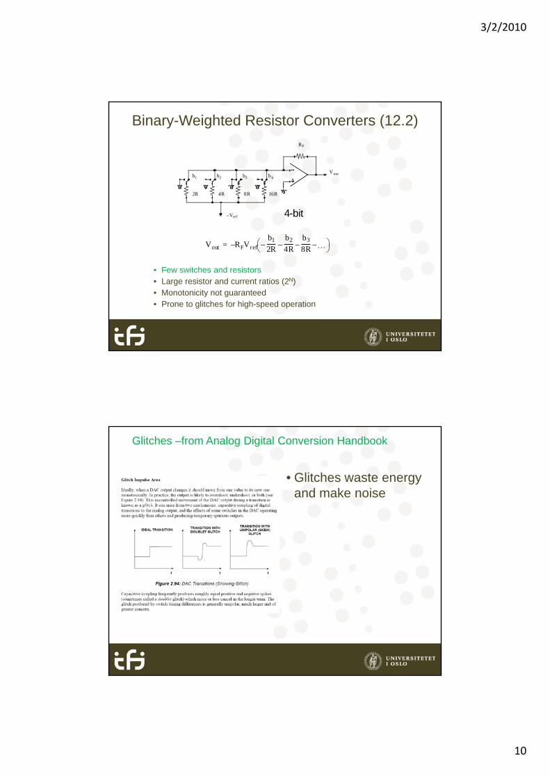
Binary-Weighted Resistor Converters (12.2)
Vout
RF
b1 b2 b3 b4
F it h d i t
16R8R4R2R
V– ref 4-bit
Vout RFVref
b1
2R-------–
b2
4R-------
b3
8R-------– ––
–=
• Few switches and resistors• Large resistor and current ratios (2N)• Monotonicity not guaranteed• Prone to glitches for high-speed operation
Glitches –from Analog Digital Conversion Handbook
• Glitches waste energy and make noise
3/2/2010
11
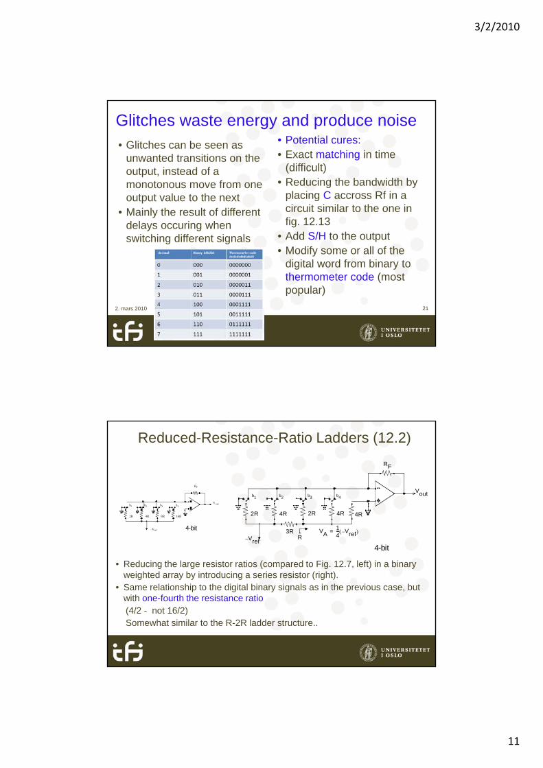
Glitches waste energy and produce noise• Glitches can be seen as
unwanted transitions on the output, instead of a monotonous move from one
• Potential cures:• Exact matching in time
(difficult)• Reducing the bandwidth bymonotonous move from one
output value to the next• Mainly the result of different
delays occuring when switching different signals
• Reducing the bandwidth by placing C accross Rf in a circuit similar to the one in fig. 12.13
• Add S/H to the output• Modify some or all of the
digital word from binary todigital word from binary to thermometer code (most popular)
2. mars 2010 21
Reduced-Resistance-Ratio Ladders (12.2)
Vout
RF
b1 b2 b3 b4V
RF
• Reducing the large resistor ratios (compared to Fig. 12.7, left) in a binary weighted array by introducing a series resistor (right).S l ti hi t th di it l bi i l i th i b t
4R2R4R2R
V– ref
3R
4R
VA14--- Vref– =
R
4-bit
Vout
16R8R4R2R
b1 b2 b3 b4
V– ref 4-bit
• Same relationship to the digital binary signals as in the previous case, but with one-fourth the resistance ratio (4/2 - not 16/2)Somewhat similar to the R-2R ladder structure..

3/2/2010
12
R-2R ladder
R-2R-Based Converters (12.2)
R R R 2R
V
R1 R'1 R'2R2 R'3R3 R'4R4
• Only two resistor values
2R2R2R2R
Vref2R
-----------Vref4R
-----------Vref8R
-----------Vref16R-----------
Vref
R'4 2R=
• Improved matching• smaller size and better
accuracy
4
R4 2R 2R R= =
R'3 R R4+ 2R= =
R3 2R R'3 R= =
3/2/2010
13
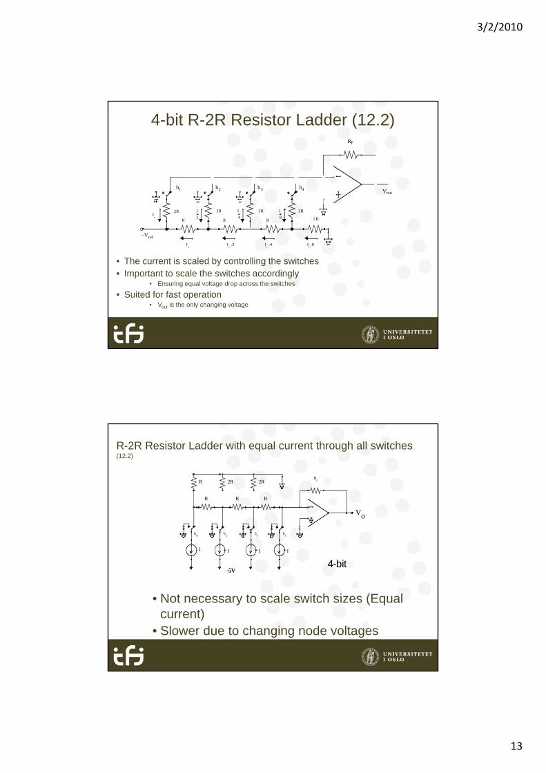
4-bit R-2R Resistor Ladder (12.2)RF
• The current is scaled by controlling the switches
Voutb1 b2 b3 b4
2R 2R 2R 2R
2 RRRRIr
Ir
Ir
2 Ir
4 Ir
8
Vref–
Ir8---
Ir
4---
Ir
2---
• Important to scale the switches accordingly• Ensuring equal voltage drop across the switches
• Suited for fast operation• Vout is the only changing voltage
R-2R Resistor Ladder with equal current through all switches (12.2)
RRR
R 2R 2RR
f
b1
b2
b3
b4
II I I
Vo
-5V4-bit
• Not necessary to scale switch sizes (Equal current)
• Slower due to changing node voltages
3/2/2010
14
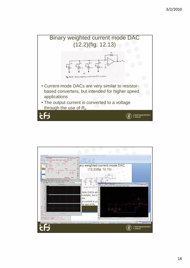
Binary weighted current mode DAC (12.2)(fig. 12.13)
• Current-mode DACs are very similar to resistor-based converters, but intended for higher speedbased converters, but intended for higher speed applications
• The output current is converted to a voltage through the use of RF
• The upper portion of each current source remains at ground potential

3/2/2010
15
Parallel charge sharing DAC principle
Capacitance ratios defining voltage gain

3/2/2010
16
Charge-Redistribution Switched Capacitor Converter (12.2) (fig. 12.12)
Vout
1
2
8C 4C 2C C
16C
• By replacing the input capacitor of an SC gain amplifier by a programmable capacitor array (PCA) a charge based converter is obtained
Vref
1
1 2
2 1
2
b1 b2 b3 b4
8C 4C 2C C
C2
4-bit
(PCA) a charge based converter is obtained• Employs correlated double sampling (CDS) – insensitive to 1/f noise, input-offset voltage and
finite amplifier gain.• An additional sign bit may be realized by interchanging the clock phases• Carefully generated clock waveforms and a deglitching capacitor are required• Digital codes must change only when the input-side of the capacitors are connected to
ground
Thermometer-Code Converters (Chapter 12.3)- number of 1s represents the decimal value
• + compared to binary counterpart:
• Lower DNL errors
decimal Binary b1b2b3 Thermometer coded1d2d3d4d5d6d7
0 000 0000000o e e o s• Reduced glitching noise• Guaranteed monotonicity• - compared to binary
counterp.:• Need 2N – 1 digital inputs
1 001 0000001
2 010 0000011
3 011 0000111
4 100 0001111
5 101 0011111
6 110 0111111eed d g a pu sto represent 2N input values
7 111 1111111

3/2/2010
17
Thermometer Based 3-bit DAC (12.3)
Rf
b1 b2 b3
Binary-to-thermometer code conversion
R R R R R R R
d1 d2 d3 d4 d5 d6 d7
f
Vout
Vref–
d1 d2 d3 d4 d5 d6 d7
• Equal resistor sizes• Equal switch sizes• 2N resistors required
Thermometer-Code Charge-Redistribution DAC (12.3) (Fig. 12.16)
• 2N capacitors requiredC
Vref -+
Vout
2NC01
02 01
02
01
C
C
C
C
Top Capacitors areConnected to G round
Bottom Capaci tors areConnected to Vref
02C 2
C
3/2/2010
18
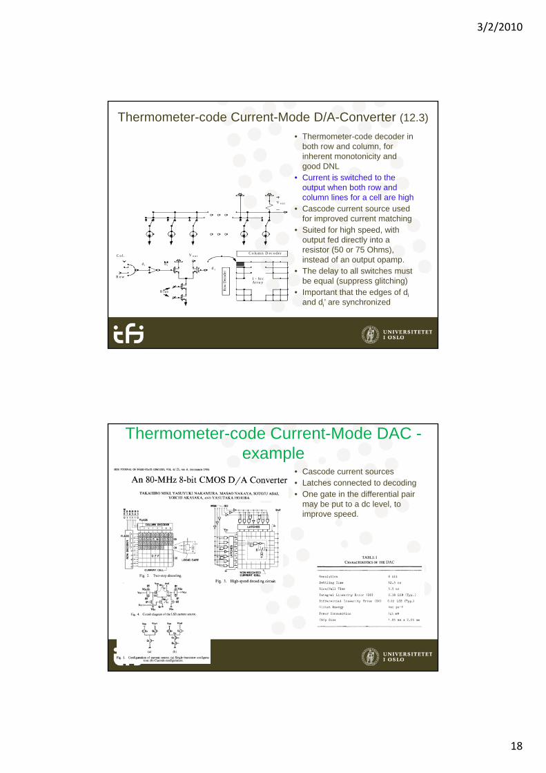
Thermometer-code Current-Mode D/A-Converter (12.3)
• Thermometer-code decoder in both row and column, for inherent monotonicity and good DNL
• Current is switched to the output when both row and column lines for a cell are high
• Cascode current source used for improved current matching
• Suited for high speed, with output fed directly into a resistor (50 or 75 Ohms), instead of an output opamp.
V o u t
C o lu m n D ec o d erC o l. V o u t
d id i
• The delay to all switches must be equal (suppress glitching)
• Important that the edges of di
and di’ are synchronized
I - SrcA rra y
Row
Dec
oder
R o w
B i as
d i
Thermometer-code Current-Mode DAC -example
• Cascode current sources• Latches connected to decoding• One gate in the differential pair
may be put to a dc level tomay be put to a dc level, to improve speed.
3/2/2010
19
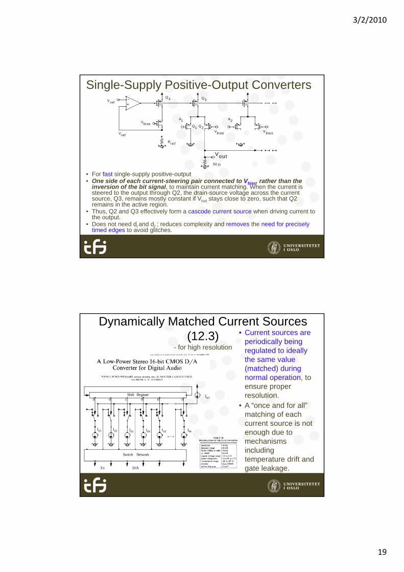
Single-Supply Positive-Output Converters –+
d1 d 2
Q2Q1
Vbi as
Q3Vref
Vb ias Vbia s
Q4
Vref
• For fast single-supply positive-output• One side of each current-steering pair connected to Vbias, rather than the
inversion of the bit signal, to maintain current matching. When the current is steered to the output through Q2, the drain-source voltage across the current
Q3 i tl t t if V t l t h th t Q2
Rre f
Vout
50
ref
source, Q3, remains mostly constant if Vout stays close to zero, such that Q2 remains in the active region.
• Thus, Q2 and Q3 effectively form a cascode current source when driving current to the output.
• Does not need di and di’ ; reduces complexity and removes the need for precisely timed edges to avoid glitches.
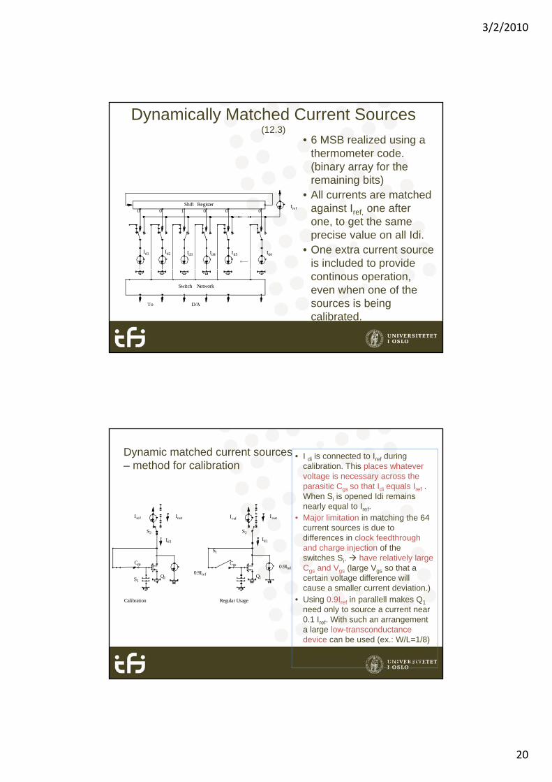
Dynamically Matched Current Sources (12.3)
- for high resolution
• Current sources are periodically being regulated to ideally the same value (matched) during normal operation, to ensure proper resolution.
• A “once and for all” matching of each current source is not enough due to
Shift Register0 0 0 0 01
Iref
Id1 Id2 Id3 Id4 Id5 I64 gmechanisms including temperature drift and gate leakage.
Switch Network
To D/A
3/2/2010
20
Dynamically Matched Current Sources (12.3)
• 6 MSB realized using a thermometer code. (binary array for the remaining bits)g )
• All currents are matched against Iref, one after one, to get the same precise value on all Idi.
• One extra current source is included to provide
Shift Register0 0 0 0 01
Iref
Id1 Id2 Id3 Id4 Id5 I64
continous operation, even when one of the sources is being calibrated.
Switch Network
To D/A
Dynamic matched current sources – method for calibration
• I di is connected to Iref during calibration. This places whatever voltage is necessary across the parasitic Cgs so that Idi equals Iref . When Si is opened Idi remains nearly equal to Iref.
• Major limitation in matching the 64 current sources is due to differences in clock feedthrough and charge injection of the switches Si. have relatively large Cgs and Vgs (large Vgs so that a certain voltage difference will cause a smaller current deviation.)
Cgs
Q1S1
S2
Cgs
Q1
S1
S2
0.9Iref0.9Iref
Iref IrefIout Iout
Id1 Id1
• Using 0.9Iref in parallell makes Q1
need only to source a current near 0.1 Iref. With such an arrangement a large low-transconductance device can be used (ex.: W/L=1/8)
• Recalibration due to leakage every 1.7 ms for [Schouwenaars, 1988]
Calibration Regular Usage

3/2/2010
21
12.4 Hybrid Converters
• Combination of different techniques, like for example decoder based, binary scaled, and thermometer-code convertersthermometer code converters
• Hybrid converters combine the advantages of different approaches for better performance
• Example: Thermometer code used for MSBs, while using a binary-scaled technique for the lower LSBs to reduce glitching. Using binary g g g yscaled for the LSBs, where glitching requirements are reduced, may save valuable chip area.
Resistor-Capacitor Hybrid Converters (12.4) • Top 7 MSBs determine
which pair of voltages across a single resistor is passed on to the 8-bit capacitor array.capacitor array.
• A 7-bit resistor-sting DAC is combined with an 8-bit SC binary-weighted DAC for a 15-bit converter
• 15-bit monotonicity, without trimming

3/2/2010
22
Segmented Converters (12.4)• Combination of
thermometer- and binary
• 2 MSB’s areVout
R/2
+-
2 MSB s are thermometer (reduces glitches)
• 4 LSB’s are binary
• High bits it h d t th
R R R R
2R 2R 2R 2R
Vref
+-
switched to the output, low bits to ground
2R 2R 2R 2R 2R-
4 Bit Binary LSB - Segment2 MSB’s
Vref
A few published DACsPublicationyear
SFDR@Nyquist [dB]
ENOB @ Nyquist
Nyquistupdate rate,[Ms/s]
Power consumpt.[mW]
Area[mm2]
Supplyvoltage[V]
Technology[nm]
other Reference
2009 >60dB 9.7 1000 188 65Currentsteering
Lin et al., ISSCC ’09
2008 80 12.9 11 119 0.8 1.8 180”currentsteering”
Radulov, APPCAS ’08
2007 59 9.5 200 @3.3 V
56 2.25 3.3 180 ”currentsteering”
Mercer, JSCC, Aug.’07
2004 40 6 250 23 0.14 1.8 180 ”binaryweighted”
Deveugele, JSCC, July ’04
2001 61 9.84 1000 110 0.35 3.0 350”currentsteering”
Van den Bosch, JSCC, Mar.’01
1988 95 15.45 0.044 15 5 2.5‐5 2000Schouwenaars, JSCC, Dec. ’88
3/2/2010
23
Next Tuesday (9/3-08):
• Chapter 13 Nyquist Analog-to-Digital Converters
Additional litterature
• Phillip E. Allen, Douglas R. Holberg: CMOS Analog Circuit Design, Holt Rinehart Winston, 1987.
• R. Gregorian, G. Temes: Analog MOS Integrated Circuits for Signal Processing, Wiley, 1986
• Leif Hanssen: High Speed Data Converters Fully Integrated in CMOS, dissertation for the dr. scient. Degree, University Of Oslo, 1990.
• A/D , D/A Conversion Handbook, Analog Devices.• Lecture Notes, University of California, Berkeley,
EE247 Analog Digital Interface Integrated Circuits, Fall 07;http://inst.eecs.berkeley.edu/~ee247/fa07/