nxq1txa1 qi-standard conforming charger controller · 1. general description the nxq1txa1 is a...
TRANSCRIPT
1. General description
The NXQ1TXA1 is a state of the art digital control controller for Qi-standard conforming wireless charger base stations. The controller supports type A1 or A10 single coil base stations.
The NXQ1TXA1 offers wireless power transfer, WPC 1.1 - Qi low-power standard-compliant communication and safety functions including Foreign Object Detection (FOD), temperature monitoring and more. The controller supports the conventional WPC pinging mode during standby to identify potential receivers. The controller can also work with the trigger function of the NXP NTAG I2C product. This feature enables wake up from a phone its NFC field while having zero power consumption of the charger during standby. The controller also offers a flexible User Interface (UI) with up to two LEDs and one buzzer for feedback and control.
Depending on the required charging pad area, coil configurations such as A1 (single coil with magnet) and A10 (single coil without magnet) are supported.
2. Features and benefits
Qi conforming wireless charger controller and communication:
Integrated Foreign Object Detection (FOD)
Using frequency and duty cycle control
ASK demodulation
One NTC input for coil or surface temperature monitoring
Two LED outputs for optical user feedback
Buzzer output for acoustical user feedback
Integrated PMU (Power Management Unit) to minimize power consumption during Sleep and power-down modes using tap to power on
Tap to power on option in combination with NT3H1201 (NFC TAG)
Temperature range 40 C to +85 C HVQFN33 package, 7 7 0.85 mm
3. Applications
Wireless Power Consortium version 1.1 (Qi) conforming base station for charging of mobile devices
NXQ1TXA1Qi-standard conforming charger controllerRev. 2 — 2 July 2015 Objective data sheet

NXP Semiconductors NXQ1TXA1Qi-standard conforming charger controller
4. Ordering information
The NXP WPC/Qi charging transmitter application uses NXP and non-NXP components to offer an optimized system solution in terms of performance and cost.
Table 1. Ordering information
Type number Package
Name Description Order information 12NC Version
NXQ1TXA1/001 HVQFN33 HVQFN: plastic thermal enhanced very thin quad flat
package; no leads; 33 terminals; body 7 7 0.85 mm
9353 039 25551 -
NXQ1TXA1 All information provided in this document is subject to legal disclaimers. © NXP Semiconductors N.V. 2015. All rights reserved.
Objective data sheet Rev. 2 — 2 July 2015 2 of 21

NXP Semiconductors NXQ1TXA1Qi-standard conforming charger controller
5. Block diagram
The block diagram does not depict all semiconductor components used to build the system. Refer to the related application note for details.
The NXQ1TXA1/001 supports A1 or A10 single coil chargers only.
Fig 1. NXQ1TXA1 based Qi compliant charger block diagram, A1/A10 (1-coil) design with NFC wake-up
aaa-014943
NFC TAG IF
NXQ1TXA1
UI CTRL
NXP component
Optional NXP components forNFC control and zero standby power
MONITOR
HALF-BRIDGECONTROL
CONTROLLER
DEMODULATOR ASK DETECTION
MODE SELECT
SE
L3
SE
L2
SE
L1
OP
T2
OP
T1
CL_MON
ASK
HALF-BRIDGEDRIVER
EN_HB
PWM
l2C
3V3
Vout
VS
NS
ISN
S
NTC
NWP2081
EN
_NFC
3V3
3V3
RESET
LED1
LED2
DC/DC
NX3008NBKW
NX3008CBKS
NX2020P1
BC847C
NX2020N2
BAS101S
NX2020N2
RSense19 V
OPTIONAL
CURRENTMONITOR
NFCNT3H1201
AC/DCTEA1720
mains110 V - 230 V ~
MODE SELECTAND
VOLTAGEREFERENCE
(TL431BFDT)
BU
ZZ
buzzer
NXQ1TXA1 All information provided in this document is subject to legal disclaimers. © NXP Semiconductors N.V. 2015. All rights reserved.
Objective data sheet Rev. 2 — 2 July 2015 3 of 21

NXP Semiconductors NXQ1TXA1Qi-standard conforming charger controller
Fig 2. NXQ1TXA1/001 internal block diagram
NXQ1TXA1 All information provided in this document is subject to legal disclaimers. © NXP Semiconductors N.V. 2015. All rights reserved.
Objective data sheet Rev. 2 — 2 July 2015 4 of 21
NXP Semiconductors NXQ1TXA1Qi-standard conforming charger controller
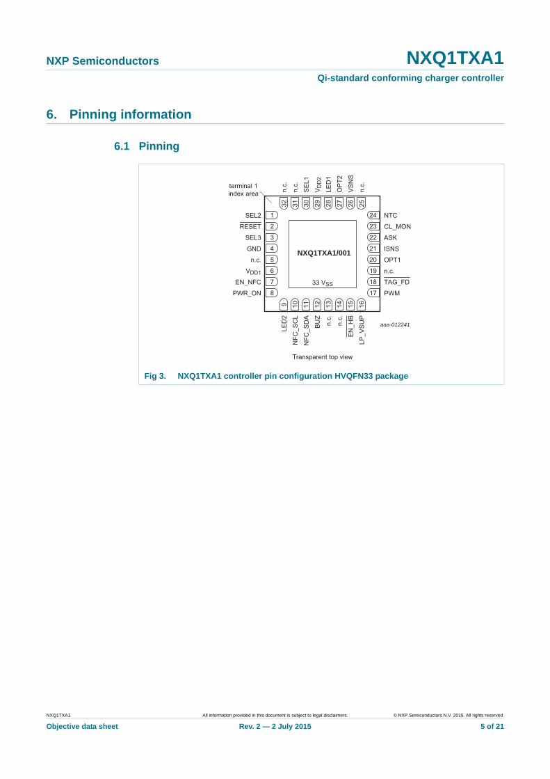
6. Pinning information
6.1 Pinning
Fig 3. NXQ1TXA1 controller pin configuration HVQFN33 package
aaa-012241
Transparent top view
PWM
EN_NFC
PWR_ON
TAG_FD
VDD1 n.c.
n.c. OPT1
GND ISNS
SEL3 ASK
RESET CL_MON
SEL2 NTC
LED
2
NFC
_SC
L
NFC
_SD
A
BU
Z
n.c.
n.c.
EN
_HB
LP_V
SU
P
n.c.
n.c.
SE
L1
VD
D2
LED
1
OP
T2
VS
NS
n.c.
8 17
7 18
6 19
5 20
4 21
3 22
2 23
1 24
9 10 11 12 13 14 15 16
32 31 30 29 28 27 26 25
terminal 1index area
33 VSS
NXQ1TXA1/001
NXQ1TXA1 All information provided in this document is subject to legal disclaimers. © NXP Semiconductors N.V. 2015. All rights reserved.
Objective data sheet Rev. 2 — 2 July 2015 5 of 21

NXP Semiconductors NXQ1TXA1Qi-standard conforming charger controller
6.2 Pin description
Table 2. NXQ1TXA1 pin description table
Symbol Pin Description
RESET 2 RESET — external reset input with 20 ns glitch filter. A LOW-going pulse as short as 50 ns on this pin resets the device.
PWR_ON 8 PWR_ON — power on signal
NFC_SCL 10 NFC_SCL — NFC Tag I2C-bus, open-drain clock input/output
NFC_SDA 11 NFC_SDA — NFC Tag I2C-bus, open-drain data input/output
TAG_FD 18 TAG_FD — field detect
EN_NFC 7 EN_NFC — NFC tag enable control output
EN_HB 15 EN_HB — half-bridge enable control
LP_VSUP 16 LP_VSUP — switched low-power voltage supply
PWM 17 PWM — half-bridge PWM control
VSNS 26 VSNS — supply voltage monitor input
ISNS 21 ISNS — current sense monitor input. Power stage current measured over 22 mwith a gain of 100 V/V.
ASK 22 ASK — ASK demodulator signal input
CL_MON 23 CL_MON — coil voltage monitor
NTC 24 NTC — NTC input pin
OPT1 20 OPT1 — option select input 1
OPT2 27 OPT2 — option select input 2 and voltage reference input
SEL1 30 SEL1 — select 1 pin
SEL2 1 SEL2 — select 2 pin
SEL3 3 SEL3 — select 3 pin
LED1 28 LED1 — LED 1 open-drain pull-down pin
LED2 9 LED2 — LED 2 open-drain pull-down
BUZ 12 BUZ — Buzzer open-drain driver input/output pin
VDD 6; 29 VDD — 3.3 V supply voltage input
VSS 33 VSS — GND and thermal pad; connect to GND
GND 4 reserved - connect to GND
n.c. 5, 13, 14, 19, 25, 31, 32
n.c. — not connected; do NOT connect to GND
NXQ1TXA1 All information provided in this document is subject to legal disclaimers. © NXP Semiconductors N.V. 2015. All rights reserved.
Objective data sheet Rev. 2 — 2 July 2015 6 of 21

NXP Semiconductors NXQ1TXA1Qi-standard conforming charger controller
7. Functional description
7.1 Functional overview
The NXQ1TXA1 is a wireless charging controller for usage in a base station with a single primary coil. It is intended to create a type A1 or type A10 power transmitter as defined by the Qi low-power specification v.1.1.2 of the Wireless Power Consortium.
Figure 1 shows that using the NXQ1TXA1 IC in combination with a power stage, creates a magnetic coupled power transmitter. The power stage comprises a half-bridge driver (NWP2081T) and two MOSFETs (NX2020N2).
The charging controller takes care of all intelligence involved to create a wireless charging transmitter. It includes the control signals PWM and EN_HB to drive a power stage, and the analog inputs ASK and CL_MON for detection and communication. An optional NTC input is used for over temperature protection.
A separate current monitor is used to enable foreign object detection. A discrete envelope detector circuit is used to reconstruct the 2 kHz ASK communication waveform as used by Qi.
At start-up, the controller senses the OPTx inputs to determine the functionality of the connected LEDs and Buzzer. The SELx pins are driven to select the settings for Foreign Object Detection. The transmitter implements four phases, as defined by the Qi standard, for power transfer from a base station to a mobile device: selection, ping, identification and configuration, and power transfer. The transitions between these four phases are done according to the Qi specification.
7.2 Configuration options
The NXQ1TXA1 supports multiple modes of operation for the user interface, comprised of two LEDs and one Buzzer. It supports several blinking code variations for the LEDs in combination with buzzer tones. The voltage level at pin OPT1, sets the UI mode of operation at start-up. To set the level at the pin OPT1, a voltage divider can be used as depicted in Figure 4.
The various settings possible are summarized in Table 3
Fig 4. UI behavior mode/option selection
OPT1
2.495 V
RS1100 kΩ
1 %
RS2
20Mode select
aaa-012238
NXQ1TXA1 All information provided in this document is subject to legal disclaimers. © NXP Semiconductors N.V. 2015. All rights reserved.
Objective data sheet Rev. 2 — 2 July 2015 7 of 21

NXP Semiconductors NXQ1TXA1Qi-standard conforming charger controller
7.3 Safety features
The NXQ1TXA1 contains three different safety functions to protect the user, the charger itself and also the mobile device to be charged.
The foreign object detection regularly evaluates whether significant amounts of power are absorbed by devices not related to the power receiver used for charging. Thermal protection is used to monitor the base station and the coil temperature. Additionally, if the receiver indicates an error condition or an end-of-charge, the controller stops the power transfer.
7.3.1 Foreign Object Detection
The Foreign Object Detection (FOD) implemented in the NXQ1TXA1 regularly compares the base station input power with the mobile side received power packet information. It calculates additional losses to foreign objects that are not accounted for in the transmitter or receiver. Once the power transfer is stopped due to a foreign object being detected, the base station waits until the receiver is removed.
When the mobile device is placed back on the power transmitter unit, the NXQ1TXA1 resumes normal operation. In case the power consuming foreign object is still present (or e.g. a mobile device is malfunctioning), the procedure is executed again. RS4 sets the FOD threshold.
The OPT2 input is being multiplexed and a voltage divider as depicted in Figure 5 can be used.
Table 3. UI behavior selection
RS1(k, 1 %)
RS2(k )
Mode number
LED Standby Charging Charge complete
FOD Temp. error
Receiver indicator error
100.0 6.7 1 reserved reserved reserved reserved reserved reserved reserved
reserved reserved reserved reserved reserved reserved reserved
100.0 14.3 2 reserved reserved reserved reserved reserved reserved reserved
reserved reserved reserved reserved reserved reserved reserved
100.0 23.2 3 reserved reserved reserved reserved reserved reserved reserved
reserved reserved reserved reserved reserved reserved reserved
100.0 33.2 4 reserved reserved reserved reserved reserved reserved reserved
reserved reserved reserved reserved reserved reserved reserved
100.0 45.3 5 reserved reserved reserved reserved reserved reserved reserved
reserved reserved reserved reserved reserved reserved reserved
100.0 60.4 6 reserved reserved reserved reserved reserved reserved reserved
reserved reserved reserved reserved reserved reserved reserved
100.0 78.7 7 reserved reserved reserved reserved reserved reserved reserved
reserved reserved reserved reserved reserved reserved reserved
100.0 100.0 8 LED1 Off Off Off 3 Hz blink 3 Hz blink 3 Hz blink
LED2 Off 1 Hz blink On Off Off Off
100.0 n.c. 16 LED1 Off Off Off Off Off Off
LED2 Off On Off 3 Hz blink 3 Hz blink 3 Hz blink
NXQ1TXA1 All information provided in this document is subject to legal disclaimers. © NXP Semiconductors N.V. 2015. All rights reserved.
Objective data sheet Rev. 2 — 2 July 2015 8 of 21

NXP Semiconductors NXQ1TXA1Qi-standard conforming charger controller
The resistors RS3 and RS4 are used with the SEL1 signal to determine the FOD threshold. The resistor settings are as in Table 4.
For FOD accuracy, a voltage of 2.495 V accurate to 0.5 % or better, must be present at the OPT2 input line when the SEL1, SEL2 and SEL3 outputs are high impedance. Resistors RS5 and RS6 are used to set the operational parameters for foreign object detection.
Fig 5. FOD threshold selection
Table 4. FOD level selection
RS3 (k, 1 %) RS4 (k, 1 %) Foreign Object Detection threshold (mW)
100.0 0 100
100.0 6.7 150
100.0 14.3 200
100.0 23.2 250
100.0 33.2 300
100.0 45.3 350
100.0 60.4 400
100.0 78.7 450
100.0 100.0 500
100.0 127.0 550
100.0 165.0 600
100.0 221.0 650
100.0 301.0 700
100.0 432.0 750
100.0 698.0 800
100.0 1500.0 850
100.0 n.c. disabled
OPT2
2.495 V
RS3100 kΩ
1 %
RS4
SEL1
27
30
1
3
Mode select
aaa-012239
SEL2
SEL3
RS5 RS6
NXQ1TXA1 All information provided in this document is subject to legal disclaimers. © NXP Semiconductors N.V. 2015. All rights reserved.
Objective data sheet Rev. 2 — 2 July 2015 9 of 21

NXP Semiconductors NXQ1TXA1Qi-standard conforming charger controller
7.3.2 Thermal protection
The voltage at pin NTC is sensed to enable the over-temperature protection. If the voltage at pin NTC drops below the high temperature threshold value, the transmitter stops the power transfer phase. It resumes when the NTC pin voltage is above the low temperature threshold value. When the transmitter resumes, it starts with the Qi selection phase again. The voltage to pin NTC can be created as shown in Figure 6.
7.3.3 Receiver end power transfer
If the active Qi receiver signals a valid end of power transfer packet, the transmitter responds according to Table 5.
Fig 6. NTC biasing and connection
VNTC
LP_VSUP
VNTClow-temp = 0.22 VDD
VNTChigh-temp = 0.17 VDD
R10 kΩ
RNTC
24Monitor
aaa-012240
Table 5. End of power transfer packet value
Reason Value base station response
Unknown 0x00 enters selection phase
Charge Complete 0x01 stop power transfer
Internal Fault 0x02 stop power transfer and waits for device removal
Over Temperature 0x03 stop power transfer and waits for device removal
Over Voltage 0x04 enters selection phase
Over Current 0x05 enters selection phase
Battery Failure 0x06 stop power transfer and waits for device removal
Reconfigure 0x07 enters identification phase
No Response 0x08 enters selection phase
Reserved 0x09 ... 0xFF stop power transfer and waits for device removal
NXQ1TXA1 All information provided in this document is subject to legal disclaimers. © NXP Semiconductors N.V. 2015. All rights reserved.
Objective data sheet Rev. 2 — 2 July 2015 10 of 21

NXP Semiconductors NXQ1TXA1Qi-standard conforming charger controller
8. Limiting values
[1] The following applies to the limiting values:
a) This product includes circuitry designed for the protection of its internal devices from the damaging effects of excessive static charge. Nonetheless, it is suggested that conventional precautions be taken to avoid applying greater than the rated maximum.
b) Parameters are valid over operating temperature range unless otherwise specified. All voltages are concerning VSS unless otherwise noted.
c) The limiting values are stress ratings only. Operating the part at these values is not recommended, and proper operation is not guaranteed. The conditions for functional operation are specified in Table 9.
[2] Maximum/minimum voltage above the maximum operating voltage (see Table 9) and below ground that can be applied for a short time (< 10 ms) to a device without leading to irrecoverable failure. Failure includes the loss of reliability and shorter lifetime of the device.
[3] VDD present or not present. Compliant with the I2C-bus standard. 5.5 V can be applied to this pin when VDD is powered down.
[4] The maximum non-operating storage temperature is different than the temperature for required shelf life which should be determined based on required shelf lifetime. Refer to the JEDEC specification (J-STD-033B.1) for further details.
[5] Human body model: equivalent to discharging a 100 pF capacitor through a 1.5 k series resistor.
Table 6. Limiting valuesIn accordance with the Absolute Maximum Rating System (IEC 60134).[1]
Symbol Parameter Conditions Min Max Unit
VDD supply voltage (core and external rail)
[2] 0.5 +4.6 V
VI input voltage 5 V tolerant I/O pins; only valid when the VDD supply voltage is present
[2] 0.5 +5.5 V
5 V tolerant open-drain pins [2][3] 0.5 +5.5 V
VIA analog input voltage pins ISNS, VSNS, NTC, ASK, CL_MON, OPTx
[2] 0.5 +4.6 V
IDD supply current per supply pin - 100 mA
ISS ground current per ground pin - 100 mA
Ilatch I/O latch-up current (0.5VDD) < VI < (1.5VDD);
Tj < 125 C
- 100 mA
Tstg storage temperature non-operating [4] 65 +150 C
Tj(max) maximum junction temperature - 150 C
Ptot total power dissipation per package based on package heat transfer, not device power consumption
- 1.5 W
VESD electrostatic discharge voltage human body model; all pins [5] - +6500 V
NXQ1TXA1 All information provided in this document is subject to legal disclaimers. © NXP Semiconductors N.V. 2015. All rights reserved.
Objective data sheet Rev. 2 — 2 July 2015 11 of 21

NXP Semiconductors NXQ1TXA1Qi-standard conforming charger controller
9. Thermal characteristics
The average chip junction temperature, Tj (C), can be calculated using the following equation:
(1)
• Tamb = ambient temperature (C)
• Rth(j-a) = the package junction-to-ambient thermal resistance (C/W)
• PD = sum of internal and I/O power dissipation
The internal power dissipation is the product of IDD and VDD. The I/O power dissipation of the I/O pins is often small and many times can be negligible.
Table 7. Thermal characteristicsVDD = 3.0 V to 3.6 V; Tamb = 40 C to +85 C unless otherwise specified.
Symbol Parameter Conditions Min Typ Max Unit
Tj(max) maximum junction temperature
- - 125 C
Table 8. NXQ1TXA1 Thermal resistance value (C/W): ±15 %VDD = 3.0 V to 3.6 V; Tamb = 40 C to +85 C unless otherwise specified.
HVQFN33
j-a
JEDEC (4.5 in 4 in)
0 m/s 40.4
1 m/s 32.7
2.5 m/s 28.3
Single-layer (4.5 in 3 in)
0 m/s 84.8
1 m/s 61.6
2.5 m/s 53.1
j-c 20.3
j-b 1.1
Tj Tamb PD Rth j a– +=
NXQ1TXA1 All information provided in this document is subject to legal disclaimers. © NXP Semiconductors N.V. 2015. All rights reserved.
Objective data sheet Rev. 2 — 2 July 2015 12 of 21

NXP Semiconductors NXQ1TXA1Qi-standard conforming charger controller
10. Static characteristics
Table 9. Static characteristics3.0 V VDD 3.6 V; Tamb = 40 C to +85 C; unless otherwise specified.
Symbol Parameter Conditions Min Typ[1] Max Unit
VDD supply voltage (core and external rail)
3.0 3.3 3.6 V
IDD supply current Active mode; average current drawn by controller during power transfer excluding output driving currents (LP_VSUP)
- 14 - mA
Standby mode; average pinging current during standby
- 5 - mA
All pins except VNTC, LP_VSUP, SCL, SDA
IIL LOW-level input current VI = 0 V - 0.5 10 nA
IIH HIGH-level input current VI = VDD - 0.5 10 nA
IOZ OFF-state output current VO = 0 V; VO = VDD - 0.5 10 nA
VO output voltage output active 0 - VDD V
VIH HIGH-level input voltage 0.7VDD - - V
VIL LOW-level input voltage - - 0.3VDD V
Vhys hysteresis voltage - 0.4 - V
VOH HIGH-level output voltage IOH = 4 mA VDD 0.4 - - V
VOL LOW-level output voltage IOL = 4 mA - - 0.4 V
IOH HIGH-level output current VOH = VDD 0.4 V 4 - - mA
IOL LOW-level output current VOL = 0.4 V 4 - - mA
IOHS HIGH-level short-circuit output current
VOH = 0 V [3] - - 45 mA
IOLS LOW-level short-circuit output current
VOL = VDD[3] - - 50 mA
VNTC (pin 24)
Vsw switch voltage NTC low temperature - 0.22VDD - V
NTC high temperature - 0.17VDD - V
LP_VSUP (pin 16)
IOZ OFF-state output current VO = 0 V; VO = VDD; - 0.5 10 nA
VO output voltage output active 0 - VDD V
VOH HIGH-level output voltage IOH = 20 mA VDD 0.4 - - V
VOL LOW-level output voltage IOL = 4 mA - - 0.4 V
IOH HIGH-level output current VOH = VDD 0.4 V;2.5 V VDD 3.6 V
20 - - mA
IOL LOW-level output current VOL = 0.4 V 4 - - mA
IOLS LOW-level short-circuit output current
VOL = VDD[3] - - 50 mA
NFC_I2C-bus pins (pin 10, pin 11)
VIH HIGH-level input voltage 0.7VDD - - V
VIL LOW-level input voltage - - 0.3VDD V
NXQ1TXA1 All information provided in this document is subject to legal disclaimers. © NXP Semiconductors N.V. 2015. All rights reserved.
Objective data sheet Rev. 2 — 2 July 2015 13 of 21

NXP Semiconductors NXQ1TXA1Qi-standard conforming charger controller
[1] Typical ratings are not guaranteed. The values listed are at room temperature (25 C), nominal supply voltages.
[2] Tamb = 25 C.
[3] Allowed as long as the current limit does not exceed the maximum current allowed by the device.
[4] To VSS.
Vhys hysteresis voltage - 0.05VDD - V
IOL LOW-level output current VOL = 0.4 V 3.5 - - mA
ILI input leakage current VI = VDD[4] - 2 4 A
Table 9. Static characteristics …continued3.0 V VDD 3.6 V; Tamb = 40 C to +85 C; unless otherwise specified.
Symbol Parameter Conditions Min Typ[1] Max Unit
NXQ1TXA1 All information provided in this document is subject to legal disclaimers. © NXP Semiconductors N.V. 2015. All rights reserved.
Objective data sheet Rev. 2 — 2 July 2015 14 of 21

NXP Semiconductors NXQ1TXA1Qi-standard conforming charger controller
11. Dynamic characteristics
11.1 Power-up ramp conditions
[1] See Figure 7.
[2] The wait time specifies the time the power supply levels must be at below 400 mV before ramping up.
11.2 Output pins
Table 10. Power-up characteristics3.0 V VDD 3.6 V; Tamb = 40 C to +105 C.
Symbol Parameter Conditions Min Typ Max Unit
tr rise time at t = t1: 0 < VI 400 mV [1] 0 - 500 ms
twait wait time [1] [2] 12 - - s
VI input voltage at t = t1 on pin VDD 0 - 400 mV
Fig 7. Power-up ramp
VDD
0
400 mV
twait
t = t1
tr
aaa-015493
Table 11. Output pins3.0 V VDD 3.6 V; Tamb = 40 C to +105 C.
Symbol Parameter Conditions Min Typ Max Unit
tr rise time pin configured as output 3.0 - 5.0 ns
tf fall time pin configured as output 2.5 - 5.0 ns
NXQ1TXA1 All information provided in this document is subject to legal disclaimers. © NXP Semiconductors N.V. 2015. All rights reserved.
Objective data sheet Rev. 2 — 2 July 2015 15 of 21

NXP Semiconductors NXQ1TXA1Qi-standard conforming charger controller
12. Package outline
Fig 8. Package outline HVQFN33
ReferencesOutlineversion
Europeanprojection
Issue dateIEC JEDEC JEITA
- - -
hvqfn33_po
09-03-1709-03-23
Unit
mmmaxnommin
1.000.850.80
0.050.020.00
0.27.17.06.9
4.854.704.55
7.17.06.9
0.65 4.550.750.600.45
0.1
A(1)
Dimensions
Note1. Plastic or metal protrusions of 0.075 mm maximum per side are not included.
HVQFN33: plastic thermal enhanced very thin quad flat package; no leads;33 terminals; body 7 x 7 x 0.85 mm
A1 b
0.350.280.23
c D(1) Dh E(1) Eh
4.854.704.55
e e1 e2
4.55
L v
0.1
w
0.05
y
0.08
y1
0 2.5 5 mm
scale
terminal 1index area
B AD
E
C
yCy1
X
detail X
A1A
c
b
e2
e1
e
e
AC BvCw
terminal 1index area Dh
Eh
L
9 16
32
33
25
17
24
8
1
NXQ1TXA1 All information provided in this document is subject to legal disclaimers. © NXP Semiconductors N.V. 2015. All rights reserved.
Objective data sheet Rev. 2 — 2 July 2015 16 of 21

NXP Semiconductors NXQ1TXA1Qi-standard conforming charger controller
13. Soldering
Fig 9. Reflow soldering of the HVQFN33 package
Footprint information for reflow soldering of HVQFN33 package
001aao134occupied area
solder land
solder resist
solder land plus solder paste
solder paste deposit
Dimensions in mmRemark:Stencil thickness: 0.125 mm
e = 0.65
evia = 4.25
OwDtot = 5.10 OA
PID = 7.25 PA+OA
OID = 8.20 OA
0.20 SRchamfer (4×)
0.45
DM
evia
= 1
.05
W = 0.30 CU
evia
= 4
.25
evia = 2.40
LbE
= 5
.80
CU
LbD = 5.80 CU
PIE
= 7
.25
PA+O
A
LaE
= 7
.95
CU
LaD = 7.95 CU
OIE
= 8
.20
OA
Ow
Eto
t = 5
.10
OA
EH
S =
4.8
5 C
U
DHS = 4.85 CU
4.55
SR
4.55 SR
B-side
(A-side fully covered)number of vias: 20
Solder resistcovered via
0.30 PH
0.60 SR cover
0.60 CU
SE
htot
= 2
.70
SP
SDhtot = 2.70 SP
Gap
E =
0.7
0 S
P
SP
E =
1.0
0 S
P
0.45 DMSPD = 1.00 SP
GapD = 0.70 SP
NXQ1TXA1 All information provided in this document is subject to legal disclaimers. © NXP Semiconductors N.V. 2015. All rights reserved.
Objective data sheet Rev. 2 — 2 July 2015 17 of 21

NXP Semiconductors NXQ1TXA1Qi-standard conforming charger controller
14. Abbreviations
15. Revision history
Table 12. Abbreviations
Acronym Description
ADC Analog-to-Digital Converter
ASK Amplitude Shift Keying
FOD Foreign Object Detection
RC Resistor-Capacitor
WPC Wireless Power Consortium
HB Half Bridge
NFC Near Field Communication
PWM Pulse Width Modulation
OTP OverTemperature Protection
NTC Negative Temperature Coefficient (Thermistor)
Table 13. Revision history
Document ID Release date Data sheet status Change notice Supersedes
NXQ1TXA1 v.2 20150702 Objective data sheet - NXQ1TXA1 v.1
Modifications: • Characteristic values updated
• Table 6, “WPC1.0 receiver power threshold” removed
• Data sheet reverted to Objective status
NXQ1TXA1 v.1 20140313 Preliminary data sheet - -
NXQ1TXA1 All information provided in this document is subject to legal disclaimers. © NXP Semiconductors N.V. 2015. All rights reserved.
Objective data sheet Rev. 2 — 2 July 2015 18 of 21
NXP Semiconductors NXQ1TXA1Qi-standard conforming charger controller
16. Legal information
16.1 Data sheet status
[1] Please consult the most recently issued document before initiating or completing a design.
[2] The term ‘short data sheet’ is explained in section “Definitions”.
[3] The product status of device(s) described in this document may have changed since this document was published and may differ in case of multiple devices. The latest product status information is available on the Internet at URL http://www.nxp.com.
16.2 Definitions
Draft — The document is a draft version only. The content is still under internal review and subject to formal approval, which may result in modifications or additions. NXP Semiconductors does not give any representations or warranties as to the accuracy or completeness of information included herein and shall have no liability for the consequences of use of such information.
Short data sheet — A short data sheet is an extract from a full data sheet with the same product type number(s) and title. A short data sheet is intended for quick reference only and should not be relied upon to contain detailed and full information. For detailed and full information see the relevant full data sheet, which is available on request via the local NXP Semiconductors sales office. In case of any inconsistency or conflict with the short data sheet, the full data sheet shall prevail.
Product specification — The information and data provided in a Product data sheet shall define the specification of the product as agreed between NXP Semiconductors and its customer, unless NXP Semiconductors and customer have explicitly agreed otherwise in writing. In no event however, shall an agreement be valid in which the NXP Semiconductors product is deemed to offer functions and qualities beyond those described in the Product data sheet.
16.3 Disclaimers
Limited warranty and liability — Information in this document is believed to be accurate and reliable. However, NXP Semiconductors does not give any representations or warranties, expressed or implied, as to the accuracy or completeness of such information and shall have no liability for the consequences of use of such information. NXP Semiconductors takes no responsibility for the content in this document if provided by an information source outside of NXP Semiconductors.
In no event shall NXP Semiconductors be liable for any indirect, incidental, punitive, special or consequential damages (including - without limitation - lost profits, lost savings, business interruption, costs related to the removal or replacement of any products or rework charges) whether or not such damages are based on tort (including negligence), warranty, breach of contract or any other legal theory.
Notwithstanding any damages that customer might incur for any reason whatsoever, NXP Semiconductors’ aggregate and cumulative liability towards customer for the products described herein shall be limited in accordance with the Terms and conditions of commercial sale of NXP Semiconductors.
Right to make changes — NXP Semiconductors reserves the right to make changes to information published in this document, including without limitation specifications and product descriptions, at any time and without notice. This document supersedes and replaces all information supplied prior to the publication hereof.
Suitability for use — NXP Semiconductors products are not designed, authorized or warranted to be suitable for use in life support, life-critical or safety-critical systems or equipment, nor in applications where failure or malfunction of an NXP Semiconductors product can reasonably be expected to result in personal injury, death or severe property or environmental damage. NXP Semiconductors and its suppliers accept no liability for inclusion and/or use of NXP Semiconductors products in such equipment or applications and therefore such inclusion and/or use is at the customer’s own risk.
Applications — Applications that are described herein for any of these products are for illustrative purposes only. NXP Semiconductors makes no representation or warranty that such applications will be suitable for the specified use without further testing or modification.
Customers are responsible for the design and operation of their applications and products using NXP Semiconductors products, and NXP Semiconductors accepts no liability for any assistance with applications or customer product design. It is customer’s sole responsibility to determine whether the NXP Semiconductors product is suitable and fit for the customer’s applications and products planned, as well as for the planned application and use of customer’s third party customer(s). Customers should provide appropriate design and operating safeguards to minimize the risks associated with their applications and products.
NXP Semiconductors does not accept any liability related to any default, damage, costs or problem which is based on any weakness or default in the customer’s applications or products, or the application or use by customer’s third party customer(s). Customer is responsible for doing all necessary testing for the customer’s applications and products using NXP Semiconductors products in order to avoid a default of the applications and the products or of the application or use by customer’s third party customer(s). NXP does not accept any liability in this respect.
Limiting values — Stress above one or more limiting values (as defined in the Absolute Maximum Ratings System of IEC 60134) will cause permanent damage to the device. Limiting values are stress ratings only and (proper) operation of the device at these or any other conditions above those given in the Recommended operating conditions section (if present) or the Characteristics sections of this document is not warranted. Constant or repeated exposure to limiting values will permanently and irreversibly affect the quality and reliability of the device.
Terms and conditions of commercial sale — NXP Semiconductors products are sold subject to the general terms and conditions of commercial sale, as published at http://www.nxp.com/profile/terms, unless otherwise agreed in a valid written individual agreement. In case an individual agreement is concluded only the terms and conditions of the respective agreement shall apply. NXP Semiconductors hereby expressly objects to applying the customer’s general terms and conditions with regard to the purchase of NXP Semiconductors products by customer.
No offer to sell or license — Nothing in this document may be interpreted or construed as an offer to sell products that is open for acceptance or the grant, conveyance or implication of any license under any copyrights, patents or other industrial or intellectual property rights.
Document status[1][2] Product status[3] Definition
Objective [short] data sheet Development This document contains data from the objective specification for product development.
Preliminary [short] data sheet Qualification This document contains data from the preliminary specification.
Product [short] data sheet Production This document contains the product specification.
NXQ1TXA1 All information provided in this document is subject to legal disclaimers. © NXP Semiconductors N.V. 2015. All rights reserved.
Objective data sheet Rev. 2 — 2 July 2015 19 of 21

NXP Semiconductors NXQ1TXA1Qi-standard conforming charger controller
Export control — This document as well as the item(s) described herein may be subject to export control regulations. Export might require a prior authorization from competent authorities.
Non-automotive qualified products — Unless this data sheet expressly states that this specific NXP Semiconductors product is automotive qualified, the product is not suitable for automotive use. It is neither qualified nor tested in accordance with automotive testing or application requirements. NXP Semiconductors accepts no liability for inclusion and/or use of non-automotive qualified products in automotive equipment or applications.
In the event that customer uses the product for design-in and use in automotive applications to automotive specifications and standards, customer (a) shall use the product without NXP Semiconductors’ warranty of the product for such automotive applications, use and specifications, and (b) whenever customer uses the product for automotive applications beyond NXP Semiconductors’ specifications such use shall be solely at customer’s
own risk, and (c) customer fully indemnifies NXP Semiconductors for any liability, damages or failed product claims resulting from customer design and use of the product for automotive applications beyond NXP Semiconductors’ standard warranty and NXP Semiconductors’ product specifications.
Translations — A non-English (translated) version of a document is for reference only. The English version shall prevail in case of any discrepancy between the translated and English versions.
16.4 TrademarksNotice: All referenced brands, product names, service names and trademarks are the property of their respective owners.
I2C-bus — logo is a trademark of NXP Semiconductors N.V.
17. Contact information
For more information, please visit: http://www.nxp.com
For sales office addresses, please send an email to: [email protected]
NXQ1TXA1 All information provided in this document is subject to legal disclaimers. © NXP Semiconductors N.V. 2015. All rights reserved.
Objective data sheet Rev. 2 — 2 July 2015 20 of 21

NXP Semiconductors NXQ1TXA1Qi-standard conforming charger controller
18. Contents
1 General description . . . . . . . . . . . . . . . . . . . . . . 1
2 Features and benefits . . . . . . . . . . . . . . . . . . . . 1
3 Applications . . . . . . . . . . . . . . . . . . . . . . . . . . . . 1
4 Ordering information. . . . . . . . . . . . . . . . . . . . . 2
5 Block diagram . . . . . . . . . . . . . . . . . . . . . . . . . . 3
6 Pinning information. . . . . . . . . . . . . . . . . . . . . . 56.1 Pinning . . . . . . . . . . . . . . . . . . . . . . . . . . . . . . . 56.2 Pin description . . . . . . . . . . . . . . . . . . . . . . . . . 6
7 Functional description . . . . . . . . . . . . . . . . . . . 77.1 Functional overview . . . . . . . . . . . . . . . . . . . . . 77.2 Configuration options . . . . . . . . . . . . . . . . . . . . 77.3 Safety features . . . . . . . . . . . . . . . . . . . . . . . . . 87.3.1 Foreign Object Detection . . . . . . . . . . . . . . . . . 87.3.2 Thermal protection . . . . . . . . . . . . . . . . . . . . . 107.3.3 Receiver end power transfer . . . . . . . . . . . . . 10
8 Limiting values. . . . . . . . . . . . . . . . . . . . . . . . . 11
9 Thermal characteristics . . . . . . . . . . . . . . . . . 12
10 Static characteristics. . . . . . . . . . . . . . . . . . . . 13
11 Dynamic characteristics . . . . . . . . . . . . . . . . . 1511.1 Power-up ramp conditions . . . . . . . . . . . . . . . 1511.2 Output pins . . . . . . . . . . . . . . . . . . . . . . . . . . . 15
12 Package outline . . . . . . . . . . . . . . . . . . . . . . . . 16
13 Soldering . . . . . . . . . . . . . . . . . . . . . . . . . . . . . 17
14 Abbreviations. . . . . . . . . . . . . . . . . . . . . . . . . . 18
15 Revision history. . . . . . . . . . . . . . . . . . . . . . . . 18
16 Legal information. . . . . . . . . . . . . . . . . . . . . . . 1916.1 Data sheet status . . . . . . . . . . . . . . . . . . . . . . 1916.2 Definitions. . . . . . . . . . . . . . . . . . . . . . . . . . . . 1916.3 Disclaimers . . . . . . . . . . . . . . . . . . . . . . . . . . . 1916.4 Trademarks. . . . . . . . . . . . . . . . . . . . . . . . . . . 20
17 Contact information. . . . . . . . . . . . . . . . . . . . . 20
18 Contents . . . . . . . . . . . . . . . . . . . . . . . . . . . . . . 21
© NXP Semiconductors N.V. 2015. All rights reserved.
For more information, please visit: http://www.nxp.comFor sales office addresses, please send an email to: [email protected]
Date of release: 2 July 2015
Document identifier: NXQ1TXA1
Please be aware that important notices concerning this document and the product(s)described herein, have been included in section ‘Legal information’.