numonyx axcelltm flash memory (p30- - digi-key sheets/numonyx,int… · · 2010-11-09data bus....
TRANSCRIPT
Datasheet Mar 20101 Order Number: 320002-10
Numonyx® AxcellTM Flash Memory (P30-65nm)256-Mbit, 512-Mbit (256M/256M)
Datasheet
Product Features
High performance— 100 ns initial access for Easy BGA— 110 ns initial access for TSOP— 25 ns 16-word asynchronous-page read mode— 52 MHz (Easy BGA) with zero WAIT states,
17ns clock-to-data output synchronous-burst read mode
— 4-, 8-, 16-, and continuous-word options for burst mode
— Buffered Enhanced Factory Programming (BEFP) at 2.0 MByte/s (Typ) using 512-word buffer
— 1.8 V buffered programming at 1.14 MByte/s (Typ) using 512-word buffer
Architecture— Multi-Level Cell Technology: Highest Density
at Lowest Cost— Asymmetrically-blocked architecture— Four 32-KByte parameter blocks: top or
bottom configuration— 128-KByte main blocks— Blank Check to verify an erased block
Voltage and Power— VCC (core) voltage: 1.7 V – 2.0 V— VCCQ (I/O) voltage: 1.7 V – 3.6 V— Standby current: 65 µA (Typ) for 256-Mbit;— 52 MHz continuos synchronous read current:
21mA (Typ)/24mA(Max)
Security— One-Time Programmable Register:
• 64 OTP bits, programmed with unique information by Numonyx• 2112 OTP bits, available for customer programming
— Absolute write protection: VPP = VSS— Power-transition erase/program lockout— Individual zero-latency block locking— Individual block lock-down— Password Access feature
Software— 25 µs (Typ) program suspend— 25 µs (Typ) erase suspend— Numonyx™ Flash Data Integrator optimized— Basic Command Set and Extended Function
Interface (EFI) Command Set compatible— Common Flash Interface capable
Density and Packaging— 56-Lead TSOP package (256-Mbit only)— 64-Ball Easy BGA package (256, 512-Mbit)— Numonyx™ QUAD+ SCSP (256, 512-Mbit)— 16-bit wide data bus
Quality and Reliability— JESD47E Compliant— Operating temperature: –40 °C to +85 °C — Minimum 100,000 erase cycles per block— 65nm process technology
Datasheet Mar 20102 Order Number: 320002-10
Legal Lines and DisclaimersINFORMATION IN THIS DOCUMENT IS PROVIDED IN CONNECTION WITH NUMONYX™ PRODUCTS. NO LICENSE, EXPRESS OR IMPLIED, BY ESTOPPEL OR OTHERWISE, TO ANY INTELLECTUAL PROPERTY RIGHTS IS GRANTED BY THIS DOCUMENT. EXCEPT AS PROVIDED IN NUMONYX'S TERMS AND CONDITIONS OF SALE FOR SUCH PRODUCTS, NUMONYX ASSUMES NO LIABILITY WHATSOEVER, AND NUMONYX DISCLAIMS ANY EXPRESS OR IMPLIED WARRANTY, RELATING TO SALE AND/OR USE OF NUMONYX PRODUCTS INCLUDING LIABILITY OR WARRANTIES RELATING TO FITNESS FOR A PARTICULAR PURPOSE, MERCHANTABILITY, OR INFRINGEMENT OF ANY PATENT, COPYRIGHT OR OTHER INTELLECTUAL PROPERTY RIGHT. Numonyx products are not intended for use in medical, life saving, life sustaining, critical control or safety systems, or in nuclear facility applications.
Numonyx B.V. may make changes to specifications and product descriptions at any time, without notice.
Numonyx B.V. may have patents or pending patent applications, trademarks, copyrights, or other intellectual property rights that relate to the presented subject matter. The furnishing of documents and other materials and information does not provide any license, express or implied, by estoppel or otherwise, to any such patents, trademarks, copyrights, or other intellectual property rights.
Designers must not rely on the absence or characteristics of any features or instructions marked “reserved” or “undefined.” Numonyx reserves these for future definition and shall have no responsibility whatsoever for conflicts or incompatibilities arising from future changes to them.
Contact your local Numonyx sales office or your distributor to obtain the latest specifications and before placing your product order.
Copies of documents which have an order number and are referenced in this document, or other Numonyx literature may be obtained by visiting Numonyx's website at http://www.numonyx.com.
Numonyx, the Numonyx logo, and Axcell are trademarks or registered trademarks of Numonyx B.V. or its subsidiaries in other countries.
*Other names and brands may be claimed as the property of others.
Copyright © 2010, Numonyx, B.V., All Rights Reserved.
Datasheet Mar 20103 Order Number: 320002-10
P30 - 65 nm
Contents
1.0 Functional Description ...............................................................................................51.1 Introduction .......................................................................................................51.2 Overview ...........................................................................................................51.3 Virtual Chip Enable Description..............................................................................61.4 Memory Maps .....................................................................................................7
2.0 Package Information .................................................................................................82.1 56-Lead TSOP.....................................................................................................82.2 64-Ball Easy BGA Package .................................................................................. 102.3 QUAD+ SCSP Packages...................................................................................... 11
3.0 Ballouts ................................................................................................................... 13
4.0 Signals .................................................................................................................... 164.1 Dual-Die Configurations ..................................................................................... 18
5.0 Bus Operations ........................................................................................................ 195.1 Reads .............................................................................................................. 195.2 Writes.............................................................................................................. 195.3 Output Disable.................................................................................................. 195.4 Standby ........................................................................................................... 205.5 Reset............................................................................................................... 20
6.0 Command Set .......................................................................................................... 216.1 Device Command Codes..................................................................................... 216.2 Device Command Bus Cycles .............................................................................. 22
7.0 Read Operation........................................................................................................ 257.1 Asynchronous Page-Mode Read ........................................................................... 257.2 Synchronous Burst-Mode Read............................................................................ 257.3 Read Device Identifier........................................................................................ 267.4 Read CFI.......................................................................................................... 26
8.0 Program Operation .................................................................................................. 278.1 Word Programming ........................................................................................... 278.2 Buffered Programming ....................................................................................... 278.3 Buffered Enhanced Factory Programming.............................................................. 288.4 Program Suspend.............................................................................................. 318.5 Program Resume............................................................................................... 318.6 Program Protection............................................................................................ 31
9.0 Erase Operations ..................................................................................................... 339.1 Block Erase ...................................................................................................... 339.2 Blank Check ..................................................................................................... 339.3 Erase Suspend.................................................................................................. 349.4 Erase Resume................................................................................................... 349.5 Erase Protection................................................................................................ 34
10.0 Security Modes ........................................................................................................ 3510.1 Block Locking.................................................................................................... 3510.2 Selectable One-Time Programmable Blocks........................................................... 3710.3 Password Access ............................................................................................... 37
11.0 Registers ................................................................................................................. 3811.1 Read Status Register ......................................................................................... 3811.2 Read Configuration Register................................................................................ 39
P30 - 65 nm
Datasheet Mar 20104 Order Number: 320002-10
11.3 One-Time-Programmable (OTP) Registers .............................................................45
12.0 Power and Reset Specifications ...............................................................................4812.1 Power-Up and Power-Down .................................................................................4812.2 Reset Specifications ...........................................................................................4812.3 Power Supply Decoupling....................................................................................49
13.0 Maximum Ratings and Operating Conditions ............................................................5013.1 Absolute Maximum Ratings .................................................................................5013.2 Operating Conditions..........................................................................................50
14.0 Electrical Specifications ...........................................................................................5114.1 DC Current Characteristics ..................................................................................5114.2 DC Voltage Characteristics ..................................................................................52
15.0 AC Characteristics ....................................................................................................5315.1 AC Test Conditions.............................................................................................5315.2 Capacitance ......................................................................................................5415.3 AC Read Specifications .......................................................................................5415.4 AC Write Specifications.......................................................................................59
16.0 Program and Erase Characteristics...........................................................................63
17.0 Ordering Information...............................................................................................6417.1 Discrete Products...............................................................................................6417.2 SCSP Products...................................................................................................65
A Supplemental Reference Information.......................................................................66A.1 Common Flash Interface Tables ...........................................................................66A.2 Flowcharts ........................................................................................................78A.3 Write State Machine...........................................................................................87
B Conventions - Additional Information ......................................................................91B.1 Conventions......................................................................................................91B.2 Acronyms .........................................................................................................91B.3 Nomenclature....................................................................................................92
C Revision History.......................................................................................................93
Datasheet Mar 20105 Order Number: 320002-10
P30-65nm
1.0 Functional Description
1.1 Introduction
This document provides information about the Numonyx® Axcell™ Flash Memory (P30-65nm) product and describes its features, operations, and specifications.
The Numonyx® Axcell™ Flash Memory (P30-65nm) is the latest generation of flash memory devices. P30-65nm device will be offered in 64-Mbit up through 2-Gbit densities. This document covers specifically 256-Mbit and 512-Mbit (256M/256M) product information. Benefits include more density in less space, high-speed interface device, and support for code and data storage. Features include high-performance synchronous-burst read mode, fast asynchronous access times, low power, flexible security options, and three industry-standard package choices. The P30-65nm product family is manufactured using Numonyx 65nm process technology.
1.2 Overview
This section provides an overview of the features and capabilities of the P30-65nm.
The P30-65nm family devices provides high performance at low voltage on a 16-bit data bus. Individually erasable memory blocks are sized for optimum code and data storage.
Upon initial power up or return from reset, the device defaults to asynchronous page-mode read. Configuring the Read Configuration Register enables synchronous burst-mode reads. In synchronous burst mode, output data is synchronized with a user-supplied clock signal. A WAIT signal provides easy CPU-to-flash memory synchronization.
In addition to the enhanced architecture and interface, the device incorporates technology that enables fast factory program and erase operations. Designed for low-voltage systems, the P30-65nm supports read operations with VCC at 1.8 V, and erase and program operations with VPP at 1.8 V or 9.0 V. Buffered Enhanced Factory Programming (BEFP) provides the fastest flash array programming performance with VPP at 9.0 V, which increases factory throughput. With VPP at 1.8 V, VCC and VPP can be tied together for a simple, ultra low power design. In addition to voltage flexibility, a dedicated VPP connection provides complete data protection when VPP ≤ VPPLK.
A Command User Interface (CUI) is the interface between the system processor and all internal operations of the device. An internal Write State Machine (WSM) automatically executes the algorithms and timings necessary for block erase and program. A Status Register indicates erase or program completion and any errors that may have occurred.
An industry-standard command sequence invokes program and erase automation. Each erase operation erases one block. The Erase Suspend feature allows system software to pause an erase cycle to read or program data in another block. Program Suspend allows system software to pause programming to read other locations. Data is programmed in word increments (16 bits).
The P30-65nm protection register allows unique flash device identification that can be used to increase system security. The individual Block Lock34
feature provides zero-latency block locking and unlocking. The P30-65nm device includes enhanced protection via Password Access; this new feature allows write and/or read access protection of user-defined blocks. In addition, the P30-65nm device also provides the One-Time Programmable (OTP) security feature backward compatible to the P30-130nm device.
P30-65nm
Datasheet Mar 20106 Order Number: 320002-10
1.3 Virtual Chip Enable Description
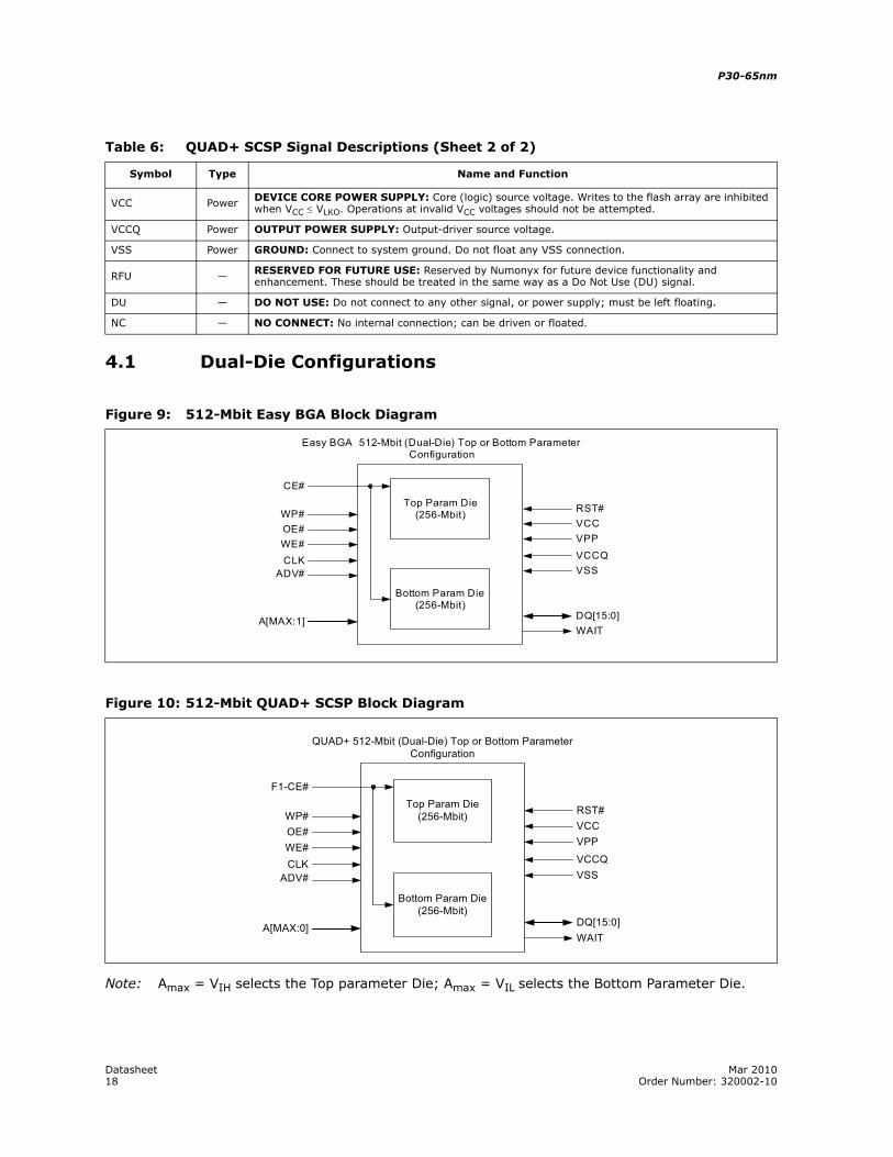
The P30-65nm 512-Mbit devices employ a Virtual Chip Enable which combines two 256-Mbit die with a common chip enable, F1-CE# for QUAD+ packages or CE# for Easy BGA packages. Refer to Figure 9 on page 18 and Figure 10 on page 18 for detail. The maximum address bit is then used to select between the die pair with F1-CE#/CE# asserted depending upon the package option used. When chip enable is asserted and The maximum address bit is low (VIL), The lower parameter die is selected; when chip enable is asserted and the maximum address bit is high (VIH), the upper parameter die is selected. Refer to Table 1 and Table 2 for additional details.
Table 1: Virtual Chip Enable Truth Table for 512 Mb (QUAD+ Package)
Die Selected F1-CE# A24
Lower Param Die L L
Upper Param Die L H
Table 2: Virtual Chip Enable Truth Table for 512 Mb (Easy BGA Packages)
Die Selected CE# A25
Lower Param Die L L
Upper Param Die L H
Datasheet Mar 20107 Order Number: 320002-10
P30-65nm
1.4 Memory Maps
Figure 1: P30-65nm Memory Map
16- Kword Block
64- Kword Block
16- Kword Block
Bottom Boot Word Wide (x16) Mode
7F 0000 - 7FFFFF
000000 – 003FFF
64- Kword Block3 F0000 - 3FFFFF
1
0
130
64- Kword BlockFF 0000 - FFFFFF 258
256-
Mbi
t
A<24:1> 256 Mbit (Easy BGA, TSOP)
16- Kword Block16- Kword Block
64- Kword Block
64- Kword Block
004000 – 007FFF
008000 – 00 BFFF
00C000 – 00 FFFF
010000 – 01 FFFF
020000 – 02 FFFF
2
3
4
5
66
16- Kword Block16- Kword Block
512 Mbit (256/256)Word Wide (x16 ) Mode
64- Kword Block
515
514
512
Mbi
t (25
6/25
6)
A<25:1 > 512 Mbit
16- Kword Block16- Kword Block
64- Kword Block
516
517
513
16- Kword Block16- Kword Block
Top Boot 256 MbitWord Wide (x16 ) Mode
64- Kword Block
256
255
256-
Mbi
t
16- Kword Block16- Kword Block
64- Kword Block
64- Kword Block
257
258
0
1
254
000000 – 00 FFFF
010000 – 01 FFFF
FF 0000 – FF3 FFF
FF 4000 – FF7 FFF
FF 8000 – FFBFFF
FFC 000 – FFFFFF
FE 0000 – FEFFFF
(256/256)
1FFC000 - 1FFFFFF
1FF8000 - 1FFBFFF
1FF4000 - 1FF7FFF
1FF0000 - 1FF3FFF
1FE0000 - 1FEFFFF
1FD0000 - 1FDFFFF 512
16- Kword Block16- Kword Block
64- Kword Block
1
0
16- Kword Block16- Kword Block
64- Kword Block
2
3
5
000C000 - 000FFFF
0008000 - 000BFFF
0004000 - 0007FFF
0000000 - 0003FFF
0020000 - 002FFFF
0010000 - 001FFFF 4
A<23: 0 > 256 Mbit (QUAD+)A<24:1> 256 Mbit (Easy BGA, TSOP)A<23: 0> 256 Mbit (QUAD+)
256 Mbit
(Easy BGA, TSOP)A<24:0 > 512 Mbit (256/256) (QUAD+)
P30-65nm
Datasheet Mar 20108 Order Number: 320002-10
2.0 Package Information
2.1 56-Lead TSOP
Figure 2: TSOP Mechanical Specifications (256-Mbit)
A
0
L
Detail A
Y
D
C
Z
Pin 1
E
D1
b
Detail B
See Detail A
e
See Detail B
A1
SeatingPlane
A2See Note 2See Notes 1 and 3
Table 3: TSOP Package Dimensions (Sheet 1 of 2)
Product Information SymbolMillimeters Inches
Min Nom Max Min Nom Max
Package Height A - - 1.200 - - 0.047
Standoff A1 0.050 - - 0.002 - -
Package Body Thickness A2 0.965 0.995 1.025 0.038 0.039 0.040
Lead Width b 0.100 0.150 0.200 0.004 0.006 0.008
Lead Thickness C 0.100 0.150 0.200 0.004 0.006 0.008
Package Body Length D1 18.200 18.400 18.600 0.717 0.724 0.732
Package Body Width E 13.800 14.000 14.200 0.543 0.551 0.559
Lead Pitch e - 0.500 - - 0.0197 -
Terminal Dimension D 19.800 20.00 20.200 0.780 0.787 0.795
Datasheet Mar 20109 Order Number: 320002-10
P30-65nm
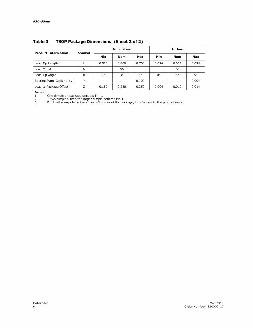
Lead Tip Length L 0.500 0.600 0.700 0.020 0.024 0.028
Lead Count N - 56 - - 56 -
Lead Tip Angle θ 0° 3° 5° 0° 3° 5°
Seating Plane Coplanarity Y - - 0.100 - - 0.004
Lead to Package Offset Z 0.150 0.250 0.350 0.006 0.010 0.014
Notes:1. One dimple on package denotes Pin 1.2. If two dimples, then the larger dimple denotes Pin 1.3. Pin 1 will always be in the upper left corner of the package, in reference to the product mark..
Table 3: TSOP Package Dimensions (Sheet 2 of 2)
Product Information SymbolMillimeters Inches
Min Nom Max Min Nom Max
P30-65nm
Datasheet Mar 201010 Order Number: 320002-10
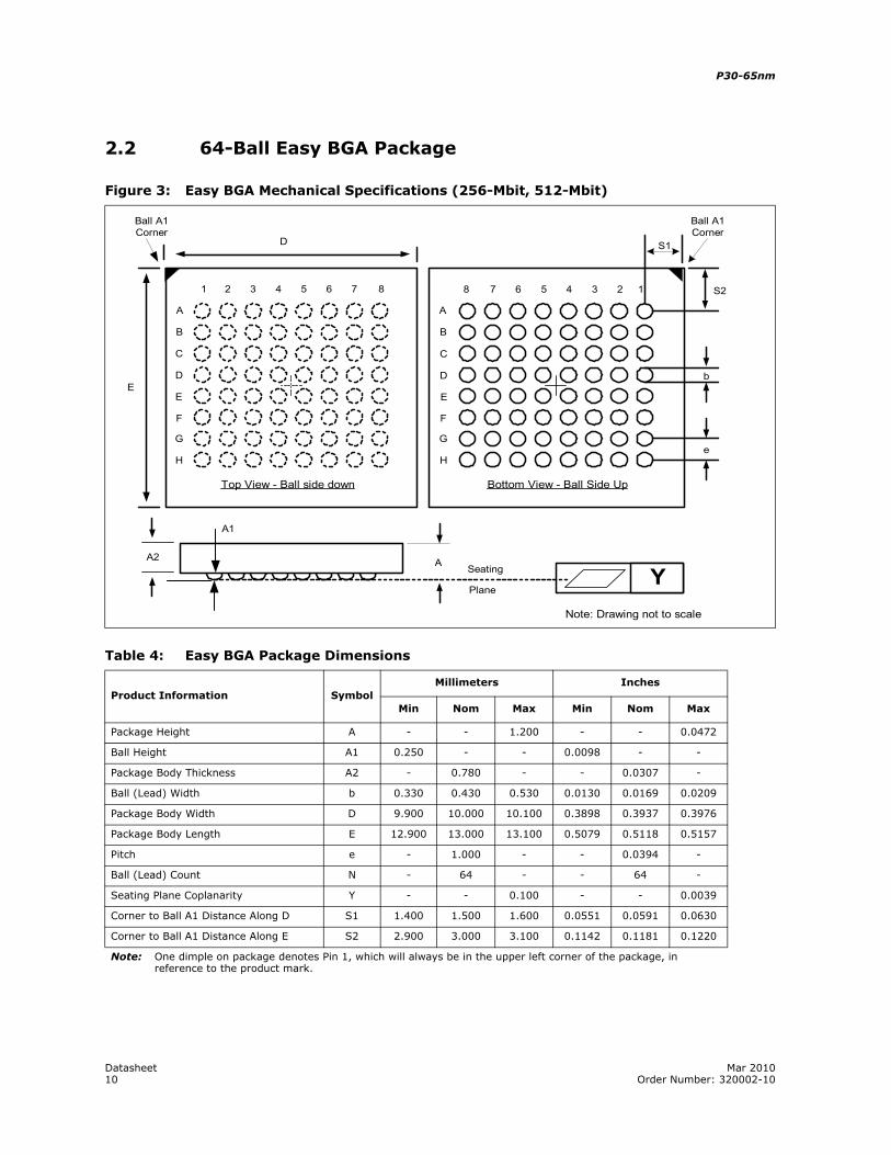
2.2 64-Ball Easy BGA Package
Figure 3: Easy BGA Mechanical Specifications (256-Mbit, 512-Mbit)
Table 4: Easy BGA Package Dimensions
Product Information SymbolMillimeters Inches
Min Nom Max Min Nom Max
Package Height A - - 1.200 - - 0.0472
Ball Height A1 0.250 - - 0.0098 - -
Package Body Thickness A2 - 0.780 - - 0.0307 -
Ball (Lead) Width b 0.330 0.430 0.530 0.0130 0.0169 0.0209
Package Body Width D 9.900 10.000 10.100 0.3898 0.3937 0.3976
Package Body Length E 12.900 13.000 13.100 0.5079 0.5118 0.5157
Pitch e - 1.000 - - 0.0394 -
Ball (Lead) Count N - 64 - - 64 -
Seating Plane Coplanarity Y - - 0.100 - - 0.0039
Corner to Ball A1 Distance Along D S1 1.400 1.500 1.600 0.0551 0.0591 0.0630
Corner to Ball A1 Distance Along E S2 2.900 3.000 3.100 0.1142 0.1181 0.1220
Note: One dimple on package denotes Pin 1, which will always be in the upper left corner of the package, in reference to the product mark.
E
Seating
Plane
S1
S2
e
Top View - Ball side down Bottom View - Ball Side Up
YA
A1
D
Ball A1Corner
A2
Note: Drawing not to scale
A
B
C
D
E
F
G
H
8 7 6 5 4 3 2 187654321
A
B
C
D
E
F
G
H
b
Ball A1Corner
Datasheet Mar 201011 Order Number: 320002-10
P30-65nm
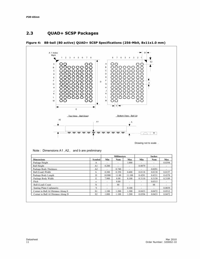
2.3 QUAD+ SCSP Packages
Figure 4: 88-ball (80 active) QUAD+ SCSP Specifications (256-Mbit, 8x11x1.0 mm)
Millimeters InchesDimensions Symbol Min Nom Max Min Nom MaxPackage Height A - - 1.000 - - 0.0394Ball Height A1 0.200 - - 0.0079 - -Package Body Thickness A2 - 0.740 - - 0.0291 -Ball (Lead) Width b 0.300 0.350 0.400 0.0118 0.0138 0.0157Package Body Length D 10.900 11.00 11.100 0.4291 0.4331 0.4370Package Body Width E 7.900 8.00 8.100 0.3110 0.3150 0.3189Pitch e - 0.80 - - 0.0315 -Ball (Lead) Count N - 88 - - 88 -Seating Plane Coplanarity Y - - 0.100 - - 0.0039Corner to Ball A1 Distance Along E S1 1.100 1.200 1.300 0.0433 0.0472 0.0512Corner to Ball A1 Distance Along D S2 1.000 1.100 1.200 0.0394 0.0433 0.0472
Top View - Ball Down Bottom View - Ball Up
AA2
D
E
Y
A1
Drawing not to scale .
S2
S1
A
C
B
E
D
G
F
J
H
K
L
M
e
12345678
b
A
C
B
E
D
G
F
J
H
K
L
M
A 1 Index Mark
1 2 3 4 5 6 7 8
Note : Dimensions A1 , A2 , and b are preliminary
P30-65nm
Datasheet Mar 201012 Order Number: 320002-10
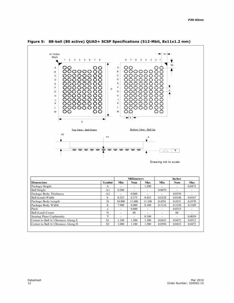
Figure 5: 88-ball (80 active) QUAD+ SCSP Specifications (512-Mbit, 8x11x1.2 mm)
Millimeters InchesDimensions Symbol Min Nom Max Min Nom MaxPackage Height A - - 1.200 - - 0.0472Ball Height A1 0.200 - - 0.0079 - -Package Body Thickness A2 - 0.860 - - 0.0339 -Ball (Lead) Width b 0.325 0.375 0.425 0.0128 0.0148 0.0167Package Body Length D 10.900 11.000 11.100 0.4291 0.4331 0.4370Package Body Width E 7.900 8.000 8.100 0.3110 0.3150 0.3189Pitch e - 0.800 - - 0.0315 -Ball (Lead) Count N - 88 - - 88 -Seating Plane Coplanarity Y - - 0.100 - - 0.0039Corner to Ball A1 Distance Along E S1 1.100 1.200 1.300 0.0433 0.0472 0.0512Corner to Ball A1 Distance Along D S2 1.000 1.100 1.200 0.0394 0.0433 0.0472
Top View - Ball Down Bottom View - Ball Up
AA2
D
E
Y
A1
Drawing not to scale .
S2
S1
A
C
B
E
D
G
F
J
H
K
L
M
e
12345678
b
A
C
B
E
D
G
F
J
H
K
L
M
A1 Index Mark
1 2 3 4 5 6 7 8
Datasheet Mar 201013 Order Number: 320002-10
P30-65nm
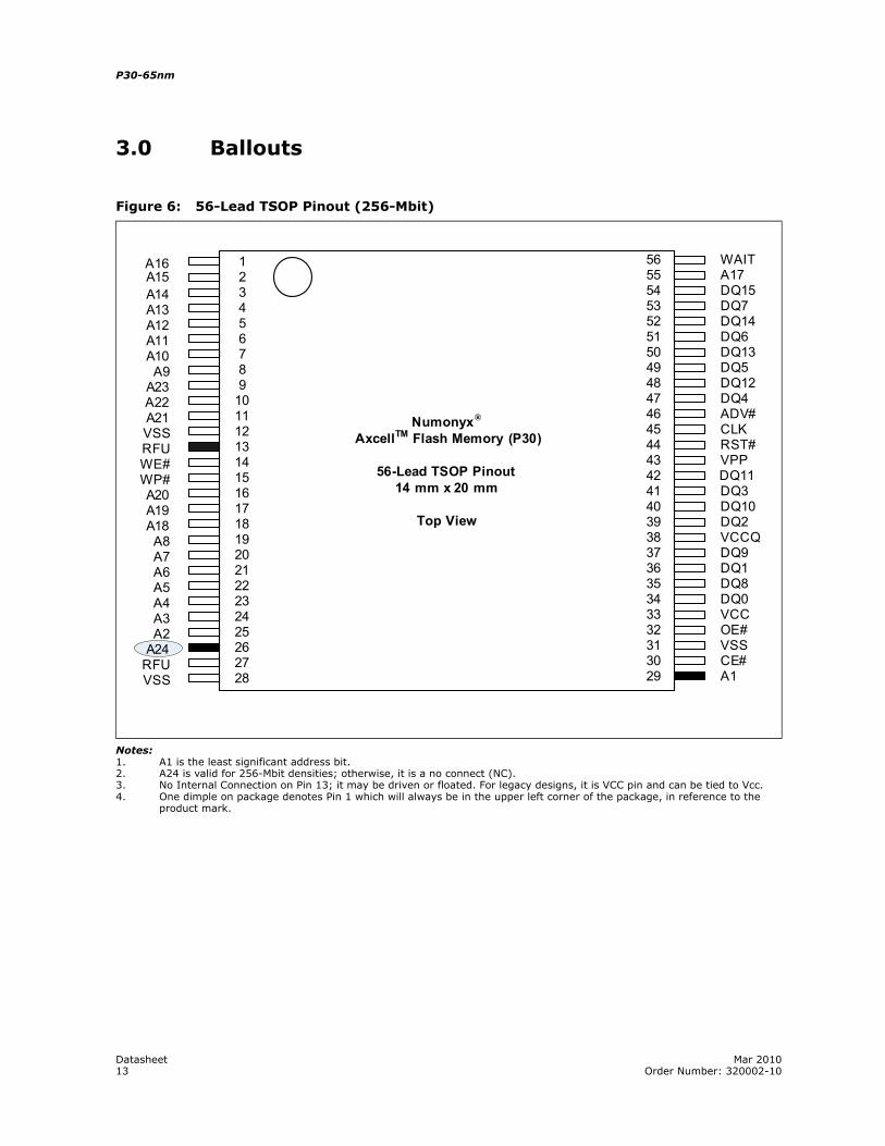
3.0 Ballouts
Notes:1. A1 is the least significant address bit.2. A24 is valid for 256-Mbit densities; otherwise, it is a no connect (NC).3. No Internal Connection on Pin 13; it may be driven or floated. For legacy designs, it is VCC pin and can be tied to Vcc.4. One dimple on package denotes Pin 1 which will always be in the upper left corner of the package, in reference to the
product mark.
Figure 6: 56-Lead TSOP Pinout (256-Mbit)
Numonyx®AxcellTM Flash Memory (P30)
56-Lead TSOP Pinout14 mm x 20 mm
Top View
1
34
2
5
78
6
9
1112
10
13
1516
14
17
1920
18
21
2324
22
25
2728
26
56
5453
55
52
5049
51
48
4645
47
44
4241
43
40
3837
39
36
3433
35
32
3029
31
A14A13A12
A10A9
A11
A23
A21VSS
A22
RFU
WP#A20
WE#
A19
A8A7
A18
A6
A4A3
A5
A2
RFUVSS
A24
WAIT
DQ15DQ7
A17
DQ14
DQ13DQ5
DQ6
DQ12
ADV#CLK
DQ4
RST#
A16
DQ3
VPP
DQ10
VCCQDQ9
DQ2
DQ1
DQ0VCC
DQ8
OE#
CE#A1
VSS
A15
DQ11
P30-65nm
Datasheet Mar 201014 Order Number: 320002-10
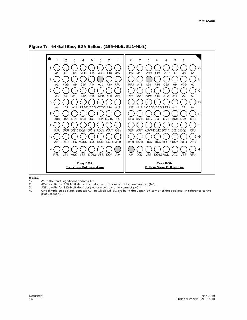
Notes:1. A1 is the least significant address bit.2. A24 is valid for 256-Mbit densities and above; otherwise, it is a no connect (NC).3. A25 is valid for 512-Mbit densities; otherwise, it is a no connect (NC).4. One dimple on package denotes A1 Pin which will always be in the upper left corner of the package, in reference to the
product mark.
Figure 7: 64-Ball Easy BGA Ballout (256-Mbit, 512-Mbit)
1 82 3 4 5 6 7
Easy BGATop View- Ball side down
Easy BGABottom View- Ball side up
18 234567
H
G
F
E
D
C
B
A
H
G
F
E
D
C
A
A2 VSS A9 A14CE# A19 RFUA25
RFU VSS VCC DQ13VSS DQ7 A24VSS
A3 A7 A10 A15A12 A20 A21WP#
A4 A5 A11 VCCQRST# A16 A17VCCQ
RFUDQ8 DQ1 DQ9 DQ4DQ3 DQ15CLK
RFU OE#DQ0 DQ10 DQ12DQ11 WAITADV#
WE#A23 RFU DQ2 DQ5VCCQ DQ14DQ6
A1 A6 A8 A13VPP A18 A22VCC
A23
A4A5A11VCCQ RST#A16A17 VCCQ
A1A6A8A13 VPPA18A22 VCC
A3A7A10A15 A12A20A21 WP#
RFU DQ8DQ1DQ9DQ4 DQ3DQ15 CLK
RFUOE# DQ0DQ10DQ12 DQ11WAIT ADV#
WE# RFUDQ2DQ5 VCCQDQ14 DQ6
A2VSSA9A14 CE#A19RFU A25
RFUVSSVCCDQ13 VSSDQ7A24 VSS
B
Datasheet Mar 201015 Order Number: 320002-10
P30-65nm
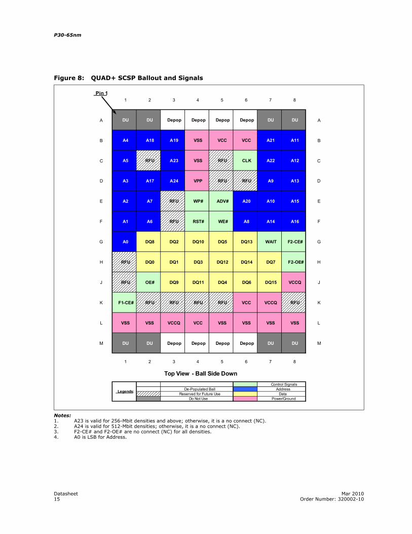
Notes:1. A23 is valid for 256-Mbit densities and above; otherwise, it is a no connect (NC).2. A24 is valid for 512-Mbit densities; otherwise, it is a no connect (NC).3. F2-CE# and F2-OE# are no connect (NC) for all densities.4. A0 is LSB for Address.
Figure 8: QUAD+ SCSP Ballout and Signals
Pin 11 2 3 4 5 6 7 8
A DU DU Depop Depop Depop Depop DU DU A
B A4 A18 A19 VSS VCC VCC A21 A11 B
C A5 RFU A23 VSS RFU CLK A22 A12 C
D A3 A17 A24 VPP RFU RFU A9 A13 D
E A2 A7 WP# ADV# A20 A10 A15 E
F A1 A6 RFU RST# WE# A8 A14 A16 F
G A0 DQ8 DQ2 DQ10 DQ5 DQ13 WAIT F2-CE# G
H RFU DQ0 DQ1 DQ3 DQ12 DQ14 DQ7 F2-OE# H
J RFU OE# DQ9 DQ11 DQ4 DQ6 DQ15 VCCQ J
K F1-CE# RFU RFU RFU RFU VCC VCCQ RFU K
L VSS VSS VCCQ VCC VSS VSS VSS VSS L
M DU DU Depop Depop Depop Depop DU DU M
1 2 3 4 5 6 7 8
Control Signals
Reserved for Future Use DataDo Not Use Power/Ground
Address
Top View - Ball Side Down
Legends: De-Populated Ball
RFU
P30-65nm
Datasheet Mar 201016 Order Number: 320002-10
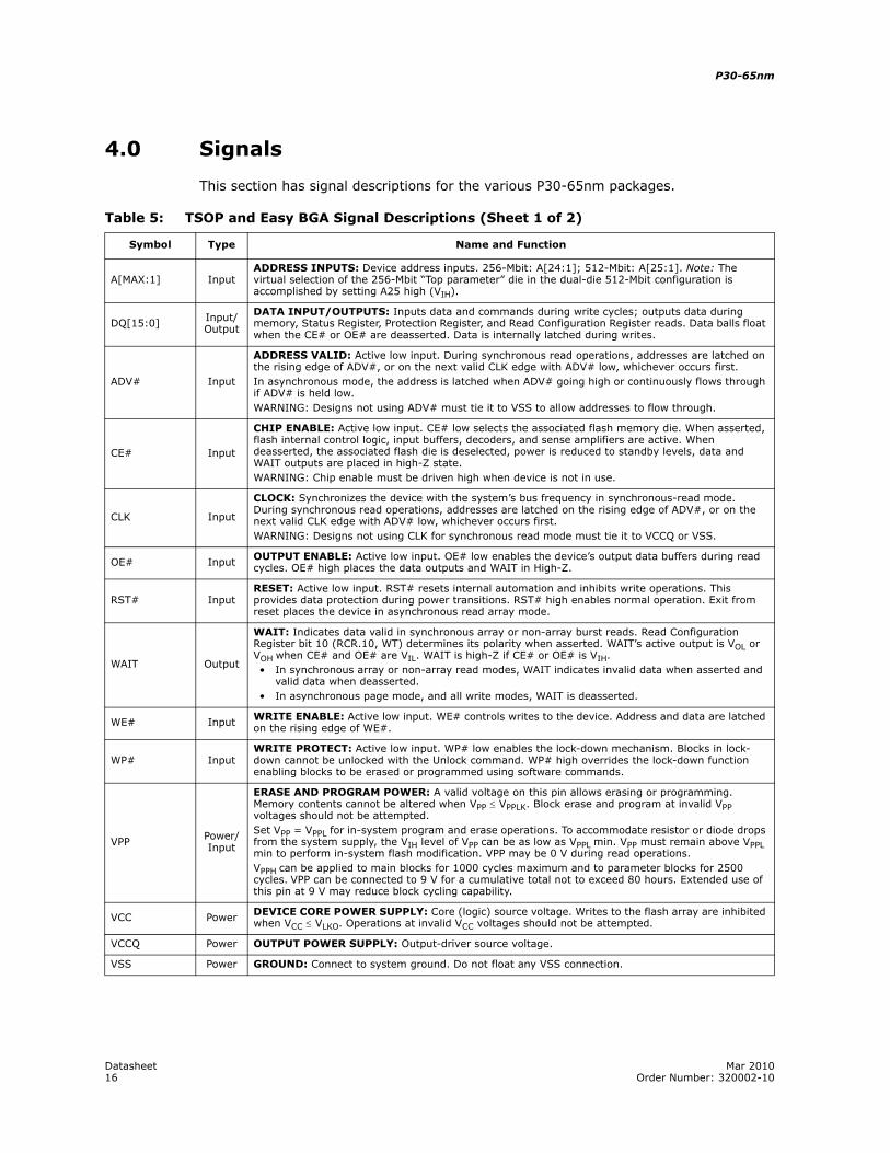
4.0 Signals
This section has signal descriptions for the various P30-65nm packages.
Table 5: TSOP and Easy BGA Signal Descriptions (Sheet 1 of 2)
Symbol Type Name and Function
A[MAX:1] InputADDRESS INPUTS: Device address inputs. 256-Mbit: A[24:1]; 512-Mbit: A[25:1]. Note: The virtual selection of the 256-Mbit “Top parameter” die in the dual-die 512-Mbit configuration is accomplished by setting A25 high (VIH).
DQ[15:0] Input/Output
DATA INPUT/OUTPUTS: Inputs data and commands during write cycles; outputs data during memory, Status Register, Protection Register, and Read Configuration Register reads. Data balls float when the CE# or OE# are deasserted. Data is internally latched during writes.
ADV# Input
ADDRESS VALID: Active low input. During synchronous read operations, addresses are latched on the rising edge of ADV#, or on the next valid CLK edge with ADV# low, whichever occurs first. In asynchronous mode, the address is latched when ADV# going high or continuously flows through if ADV# is held low. WARNING: Designs not using ADV# must tie it to VSS to allow addresses to flow through.
CE# Input
CHIP ENABLE: Active low input. CE# low selects the associated flash memory die. When asserted, flash internal control logic, input buffers, decoders, and sense amplifiers are active. When deasserted, the associated flash die is deselected, power is reduced to standby levels, data and WAIT outputs are placed in high-Z state. WARNING: Chip enable must be driven high when device is not in use.
CLK Input
CLOCK: Synchronizes the device with the system’s bus frequency in synchronous-read mode. During synchronous read operations, addresses are latched on the rising edge of ADV#, or on the next valid CLK edge with ADV# low, whichever occurs first.WARNING: Designs not using CLK for synchronous read mode must tie it to VCCQ or VSS.
OE# Input OUTPUT ENABLE: Active low input. OE# low enables the device’s output data buffers during read cycles. OE# high places the data outputs and WAIT in High-Z.
RST# InputRESET: Active low input. RST# resets internal automation and inhibits write operations. This provides data protection during power transitions. RST# high enables normal operation. Exit from reset places the device in asynchronous read array mode.
WAIT Output
WAIT: Indicates data valid in synchronous array or non-array burst reads. Read Configuration Register bit 10 (RCR.10, WT) determines its polarity when asserted. WAIT’s active output is VOL or VOH when CE# and OE# are VIL. WAIT is high-Z if CE# or OE# is VIH. • In synchronous array or non-array read modes, WAIT indicates invalid data when asserted and
valid data when deasserted.• In asynchronous page mode, and all write modes, WAIT is deasserted.
WE# Input WRITE ENABLE: Active low input. WE# controls writes to the device. Address and data are latched on the rising edge of WE#.
WP# InputWRITE PROTECT: Active low input. WP# low enables the lock-down mechanism. Blocks in lock-down cannot be unlocked with the Unlock command. WP# high overrides the lock-down function enabling blocks to be erased or programmed using software commands.
VPP Power/Input
ERASE AND PROGRAM POWER: A valid voltage on this pin allows erasing or programming. Memory contents cannot be altered when VPP ≤ VPPLK. Block erase and program at invalid VPP voltages should not be attempted.Set VPP = VPPL for in-system program and erase operations. To accommodate resistor or diode drops from the system supply, the VIH level of VPP can be as low as VPPL min. VPP must remain above VPPL min to perform in-system flash modification. VPP may be 0 V during read operations.VPPH can be applied to main blocks for 1000 cycles maximum and to parameter blocks for 2500 cycles. VPP can be connected to 9 V for a cumulative total not to exceed 80 hours. Extended use of this pin at 9 V may reduce block cycling capability.
VCC Power DEVICE CORE POWER SUPPLY: Core (logic) source voltage. Writes to the flash array are inhibited when VCC ≤ VLKO. Operations at invalid VCC voltages should not be attempted.
VCCQ Power OUTPUT POWER SUPPLY: Output-driver source voltage.
VSS Power GROUND: Connect to system ground. Do not float any VSS connection.
Datasheet Mar 201017 Order Number: 320002-10
P30-65nm
RFU — RESERVED FOR FUTURE USE: Reserved by Numonyx for future device functionality and enhancement. These should be treated in the same way as a Do Not Use (DU) signal.
DU — DO NOT USE: Do not connect to any other signal, or power supply; must be left floating.
NC — NO CONNECT: No internal connection; can be driven or floated.
Table 5: TSOP and Easy BGA Signal Descriptions (Sheet 2 of 2)
Symbol Type Name and Function
Table 6: QUAD+ SCSP Signal Descriptions (Sheet 1 of 2)
Symbol Type Name and Function
A[MAX:0] InputADDRESS INPUTS: Device address inputs. 256-Mbit: A[23:0]; 512-Mbit: A[24:0]. Note: The virtual selection of the 256-Mbit “Top parameter” die in the dual-die 512-Mbit configuration is accomplished by setting A24 high (VIH).
DQ[15:0] Input/Output
DATA INPUT/OUTPUTS: Inputs data and commands during write cycles; outputs data during memory, Status Register, Protection Register, and Read Configuration Register reads. Data balls float when the CE# or OE# are deasserted. Data is internally latched during writes.
ADV# Input
ADDRESS VALID: Active low input. During synchronous read operations, addresses are latched on the rising edge of ADV#, or on the next valid CLK edge with ADV# low, whichever occurs first. In asynchronous mode, the address is latched when ADV# going high or continuously flows through if ADV# is held low. WARNING: Designs not using ADV# must tie it to VSS to allow addresses to flow through.
F1-CE# Input
Flash CHIP ENABLE: Active low input. CE# low selects the associated flash memory die. When asserted, flash internal control logic, input buffers, decoders, and sense amplifiers are active. When deasserted, the associated flash die is deselected, power is reduced to standby levels, data and WAIT outputs are placed in high-Z state. WARNING: Chip enable must be driven high when device is not in use.
CLK Input
CLOCK: Synchronizes the device with the system’s bus frequency in synchronous-read mode. During synchronous read operations, addresses are latched on the rising edge of ADV#, or on the next valid CLK edge with ADV# low, whichever occurs first.WARNING: Designs not using CLK for synchronous read mode must tie it to VCCQ or VSS.
F1-OE# Input OUTPUT ENABLE: Active low input. OE# low enables the device’s output data buffers during read cycles. OE# high places the data outputs and WAIT in High-Z.
RST# InputRESET: Active low input. RST# resets internal automation and inhibits write operations. This provides data protection during power transitions. RST# high enables normal operation. Exit from reset places the device in asynchronous read array mode.
WAIT Output
WAIT: Indicates data valid in synchronous array or non-array burst reads. Read Configuration Register bit 10 (RCR.10, WT) determines its polarity when asserted. WAIT’s active output is VOL or VOH when CE# and OE# are VIL. WAIT is high-Z if CE# or OE# is VIH. • In synchronous array or non-array read modes, WAIT indicates invalid data when asserted and
valid data when deasserted.• In asynchronous page mode, and all write modes, WAIT is deasserted.
WE# Input WRITE ENABLE: Active low input. WE# controls writes to the device. Address and data are latched on the rising edge of WE#.
WP# InputWRITE PROTECT: Active low input. WP# low enables the lock-down mechanism. Blocks in lock-down cannot be unlocked with the Unlock command. WP# high overrides the lock-down function enabling blocks to be erased or programmed using software commands.
VPP Power/lnput
ERASE AND PROGRAM POWER: A valid voltage on this pin allows erasing or programming. Memory contents cannot be altered when VPP ≤ VPPLK. Block erase and program at invalid VPP voltages should not be attempted.Set VPP = VPPL for in-system program and erase operations. To accommodate resistor or diode drops from the system supply, the VIH level of VPP can be as low as VPPL min. VPP must remain above VPPL min to perform in-system flash modification. VPP may be 0 V during read operations.VPPH can be applied to main blocks for 1000 cycles maximum and to parameter blocks for 2500 cycles. VPP can be connected to 9 V for a cumulative total not to exceed 80 hours. Extended use of this pin at 9 V may reduce block cycling capability.
P30-65nm
Datasheet Mar 201018 Order Number: 320002-10
4.1 Dual-Die Configurations
Note: Amax = VIH selects the Top parameter Die; Amax = VIL selects the Bottom Parameter Die.
VCC Power DEVICE CORE POWER SUPPLY: Core (logic) source voltage. Writes to the flash array are inhibited when VCC ≤ VLKO. Operations at invalid VCC voltages should not be attempted.
VCCQ Power OUTPUT POWER SUPPLY: Output-driver source voltage.
VSS Power GROUND: Connect to system ground. Do not float any VSS connection.
RFU — RESERVED FOR FUTURE USE: Reserved by Numonyx for future device functionality and enhancement. These should be treated in the same way as a Do Not Use (DU) signal.
DU — DO NOT USE: Do not connect to any other signal, or power supply; must be left floating.
NC — NO CONNECT: No internal connection; can be driven or floated.
Table 6: QUAD+ SCSP Signal Descriptions (Sheet 2 of 2)
Symbol Type Name and Function
Figure 9: 512-Mbit Easy BGA Block Diagram
Top Param Die(256-Mbit)
Bottom Param Die(256-Mbit)
WP#
CLK
CE#
ADV#
OE#
WAIT
WE#
RST#VCCVPP
DQ[15:0]A[MAX:1]
VCCQVSS
Easy BGA 512-Mbit (Dual-Die) Top or Bottom Parameter Configuration
Figure 10: 512-Mbit QUAD+ SCSP Block Diagram
Top Param Die(256-Mbit)
Bottom Param Die(256-Mbit)
WP#
CLK
F1-CE#
ADV#
OE#
WAIT
WE#
RST#VCCVPP
DQ[15:0]A[MAX:0]
VCCQVSS
QUAD+ 512-Mbit (Dual-Die) Top or Bottom Parameter Configuration
Datasheet Mar 201019 Order Number: 320002-10
P30-65nm
5.0 Bus Operations
CE# low and RST# high enable device read operations. The device internally decodes upper address inputs to determine the accessed block. ADV# low opens the internal address latches. OE# low activates the outputs and gates selected data onto the I/O bus.
In asynchronous mode, the address is latched when ADV# goes high or continuously flows through if ADV# is held low. In synchronous mode, the address is latched by the first of either the rising ADV# edge or the next valid CLK edge with ADV# low (WE# and RST# must be VIH; CE# must be VIL).
Bus cycles to/from the P30-65nm device conform to standard microprocessor bus operations. Table 7 summarizes the bus operations and the logic levels that must be applied to the device control signal inputs.
5.1 Reads
To perform a read operation, RST# and WE# must be deasserted while CE# and OE# are asserted. CE# is the device-select control. When asserted, it enables the flash memory device. OE# is the data-output control. When asserted, the addressed flash memory data is driven onto the I/O bus.
5.2 Writes
To perform a write operation, both CE# and WE# are asserted while RST# and OE# are deasserted. During a write operation, address and data are latched on the rising edge of WE# or CE#, whichever occurs first. Table 9, “Command Bus Cycles” on page 23 shows the bus cycle sequence for each of the supported device commands, while Table 8, “Command Codes and Definitions” on page 21 describes each command. See Section 15.0, “AC Characteristics” on page 53 for signal-timing details.
Note: Write operations with invalid VCC and/or VPP voltages can produce spurious results and should not be attempted.
5.3 Output Disable
When OE# is deasserted, device outputs DQ[15:0] are disabled and placed in a high-impedance (High-Z) state, WAIT is also placed in High-Z.
Table 7: Bus Operations Summary
Bus Operation RST# CLK ADV# CE# OE# WE# WAIT DQ[15:0] Notes
ReadAsynchronous VIH X L L L H Deasserted Output
Synchronous VIH Running L L L H Driven Output
Write VIH X L L H L High-Z Input 1
Output Disable VIH X X L H H High-Z High-Z 2
Standby VIH X X H X X High-Z High-Z 2
Reset VIL X X X X X High-Z High-Z 2,3
Notes:1. Refer to the Table 9, “Command Bus Cycles” on page 23 for valid DQ[15:0] during a write
operation.2. X = Don’t Care (H or L).3. RST# must be at VSS ± 0.2 V to meet the maximum specified power-down current.
P30-65nm
Datasheet Mar 201020 Order Number: 320002-10
5.4 Standby
When CE# is deasserted the device is deselected and placed in standby, substantially reducing power consumption. In standby, the data outputs are placed in High-Z, independent of the level placed on OE#. Standby current, ICCS, is the average current measured over any 5 ms time interval, 5 μs after CE# is deasserted. During standby, average current is measured over the same time interval 5 μs after CE# is deasserted.
When the device is deselected (while CE# is deasserted) during a program or erase operation, it continues to consume active power until the program or erase operation is completed.
5.5 Reset
As with any automated device, it is important to assert RST# when the system is reset. When the system comes out of reset, the system processor attempts to read from the flash memory if it is the system boot device. If a CPU reset occurs with no flash memory reset, improper CPU initialization may occur because the flash memory may be providing status information rather than array data. Flash memory devices from Numonyx allow proper CPU initialization following a system reset through the use of the RST# input. RST# should be controlled by the same low-true reset signal that resets the system CPU.
After initial power-up or reset, the device defaults to asynchronous Read Array mode, and the Status Register is set to 0x80. Asserting RST# de-energizes all internal circuits, and places the output drivers in High-Z. When RST# is asserted, the device shuts down the operation in progress, a process which takes a minimum amount of time to complete. When RST# has been deasserted, the device is reset to asynchronous Read Array state.
Note: If RST# is asserted during a program or erase operation, the operation is terminated and the memory contents at the aborted location (for a program) or block (for an erase) are no longer valid, because the data may have been only partially written or erased.
When returning from a reset (RST# deasserted), a minimum wait is required before the initial read access outputs valid data. Also, a minimum delay is required after a reset before a write cycle can be initiated. After this wake-up interval passes, normal operation is restored. See Section 15.0, “AC Characteristics” on page 53 for details about signal-timing.
Datasheet Mar 201021 Order Number: 320002-10
P30-65nm
6.0 Command Set
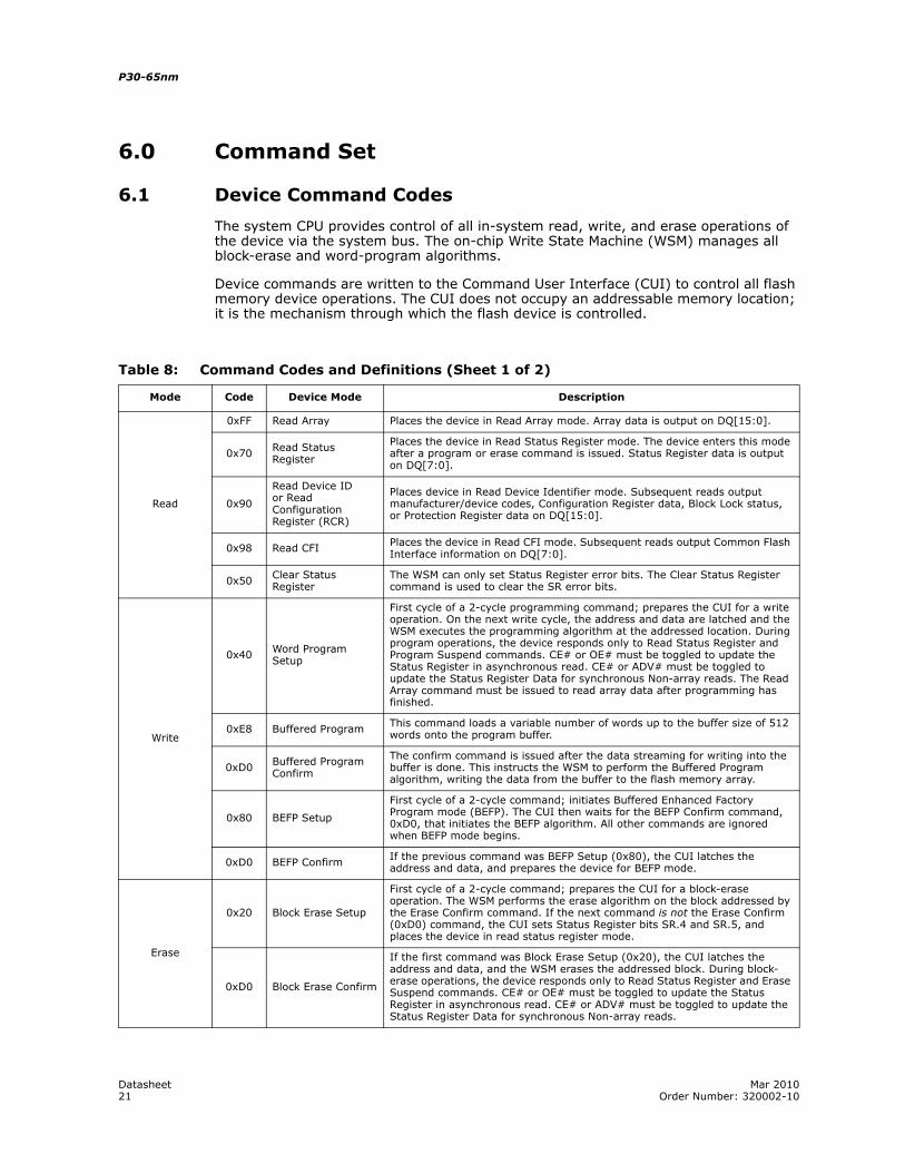
6.1 Device Command Codes
The system CPU provides control of all in-system read, write, and erase operations of the device via the system bus. The on-chip Write State Machine (WSM) manages all block-erase and word-program algorithms.
Device commands are written to the Command User Interface (CUI) to control all flash memory device operations. The CUI does not occupy an addressable memory location; it is the mechanism through which the flash device is controlled.
Table 8: Command Codes and Definitions (Sheet 1 of 2)
Mode Code Device Mode Description
Read
0xFF Read Array Places the device in Read Array mode. Array data is output on DQ[15:0].
0x70 Read Status Register
Places the device in Read Status Register mode. The device enters this mode after a program or erase command is issued. Status Register data is output on DQ[7:0].
0x90
Read Device ID or Read Configuration Register (RCR)
Places device in Read Device Identifier mode. Subsequent reads output manufacturer/device codes, Configuration Register data, Block Lock status, or Protection Register data on DQ[15:0].
0x98 Read CFI Places the device in Read CFI mode. Subsequent reads output Common Flash Interface information on DQ[7:0].
0x50 Clear Status Register
The WSM can only set Status Register error bits. The Clear Status Register command is used to clear the SR error bits.
Write
0x40 Word Program Setup
First cycle of a 2-cycle programming command; prepares the CUI for a write operation. On the next write cycle, the address and data are latched and the WSM executes the programming algorithm at the addressed location. During program operations, the device responds only to Read Status Register and Program Suspend commands. CE# or OE# must be toggled to update the Status Register in asynchronous read. CE# or ADV# must be toggled to update the Status Register Data for synchronous Non-array reads. The Read Array command must be issued to read array data after programming has finished.
0xE8 Buffered Program This command loads a variable number of words up to the buffer size of 512 words onto the program buffer.
0xD0 Buffered Program Confirm
The confirm command is issued after the data streaming for writing into the buffer is done. This instructs the WSM to perform the Buffered Program algorithm, writing the data from the buffer to the flash memory array.
0x80 BEFP Setup
First cycle of a 2-cycle command; initiates Buffered Enhanced Factory Program mode (BEFP). The CUI then waits for the BEFP Confirm command, 0xD0, that initiates the BEFP algorithm. All other commands are ignored when BEFP mode begins.
0xD0 BEFP Confirm If the previous command was BEFP Setup (0x80), the CUI latches the address and data, and prepares the device for BEFP mode.
Erase
0x20 Block Erase Setup
First cycle of a 2-cycle command; prepares the CUI for a block-erase operation. The WSM performs the erase algorithm on the block addressed by the Erase Confirm command. If the next command is not the Erase Confirm (0xD0) command, the CUI sets Status Register bits SR.4 and SR.5, and places the device in read status register mode.
0xD0 Block Erase Confirm
If the first command was Block Erase Setup (0x20), the CUI latches the address and data, and the WSM erases the addressed block. During block-erase operations, the device responds only to Read Status Register and Erase Suspend commands. CE# or OE# must be toggled to update the Status Register in asynchronous read. CE# or ADV# must be toggled to update the Status Register Data for synchronous Non-array reads.
P30-65nm
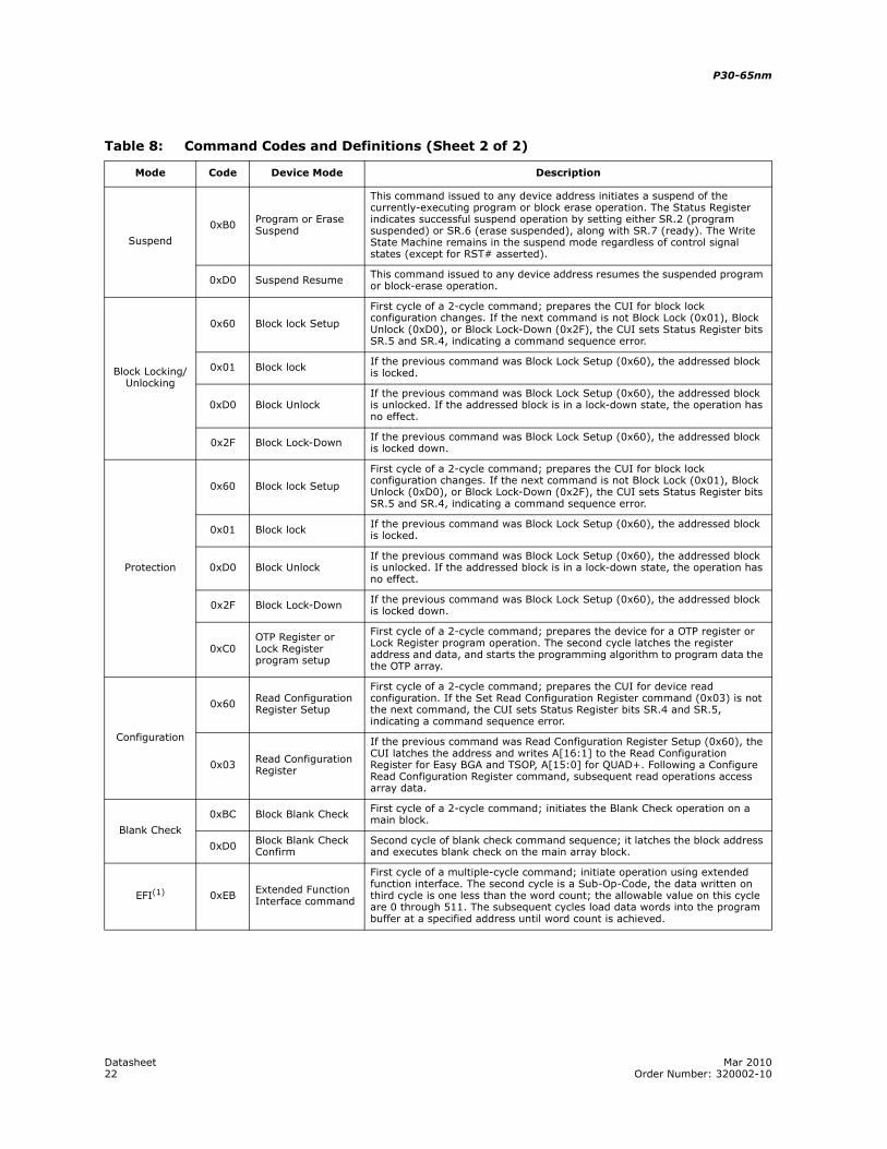
Datasheet Mar 201022 Order Number: 320002-10
Suspend
0xB0 Program or Erase Suspend
This command issued to any device address initiates a suspend of the currently-executing program or block erase operation. The Status Register indicates successful suspend operation by setting either SR.2 (program suspended) or SR.6 (erase suspended), along with SR.7 (ready). The Write State Machine remains in the suspend mode regardless of control signal states (except for RST# asserted).
0xD0 Suspend Resume This command issued to any device address resumes the suspended program or block-erase operation.
Block Locking/Unlocking
0x60 Block lock Setup
First cycle of a 2-cycle command; prepares the CUI for block lock configuration changes. If the next command is not Block Lock (0x01), Block Unlock (0xD0), or Block Lock-Down (0x2F), the CUI sets Status Register bits SR.5 and SR.4, indicating a command sequence error.
0x01 Block lock If the previous command was Block Lock Setup (0x60), the addressed block is locked.
0xD0 Block Unlock If the previous command was Block Lock Setup (0x60), the addressed block is unlocked. If the addressed block is in a lock-down state, the operation has no effect.
0x2F Block Lock-Down If the previous command was Block Lock Setup (0x60), the addressed block is locked down.
Protection
0x60 Block lock Setup
First cycle of a 2-cycle command; prepares the CUI for block lock configuration changes. If the next command is not Block Lock (0x01), Block Unlock (0xD0), or Block Lock-Down (0x2F), the CUI sets Status Register bits SR.5 and SR.4, indicating a command sequence error.
0x01 Block lock If the previous command was Block Lock Setup (0x60), the addressed block is locked.
0xD0 Block Unlock If the previous command was Block Lock Setup (0x60), the addressed block is unlocked. If the addressed block is in a lock-down state, the operation has no effect.
0x2F Block Lock-Down If the previous command was Block Lock Setup (0x60), the addressed block is locked down.
0xC0OTP Register or Lock Register program setup
First cycle of a 2-cycle command; prepares the device for a OTP register or Lock Register program operation. The second cycle latches the register address and data, and starts the programming algorithm to program data the the OTP array.
Configuration
0x60 Read Configuration Register Setup
First cycle of a 2-cycle command; prepares the CUI for device read configuration. If the Set Read Configuration Register command (0x03) is not the next command, the CUI sets Status Register bits SR.4 and SR.5, indicating a command sequence error.
0x03 Read Configuration Register
If the previous command was Read Configuration Register Setup (0x60), the CUI latches the address and writes A[16:1] to the Read Configuration Register for Easy BGA and TSOP, A[15:0] for QUAD+. Following a Configure Read Configuration Register command, subsequent read operations access array data.
Blank Check
0xBC Block Blank Check First cycle of a 2-cycle command; initiates the Blank Check operation on a main block.
0xD0 Block Blank Check Confirm
Second cycle of blank check command sequence; it latches the block address and executes blank check on the main array block.
EFI(1) 0xEB Extended Function Interface command
First cycle of a multiple-cycle command; initiate operation using extended function interface. The second cycle is a Sub-Op-Code, the data written on third cycle is one less than the word count; the allowable value on this cycle are 0 through 511. The subsequent cycles load data words into the program buffer at a specified address until word count is achieved.
Table 8: Command Codes and Definitions (Sheet 2 of 2)
Mode Code Device Mode Description
Datasheet Mar 201023 Order Number: 320002-10
P30-65nm
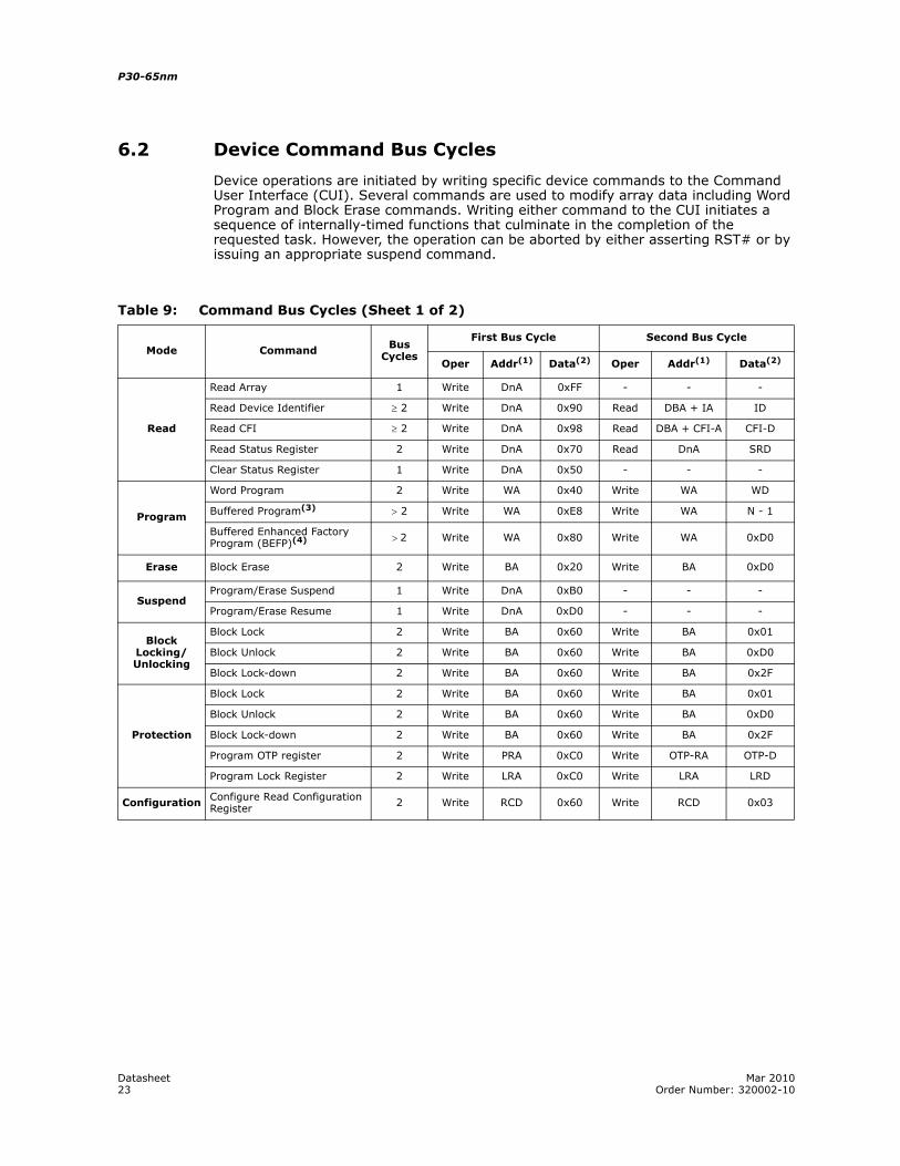
6.2 Device Command Bus Cycles
Device operations are initiated by writing specific device commands to the Command User Interface (CUI). Several commands are used to modify array data including Word Program and Block Erase commands. Writing either command to the CUI initiates a sequence of internally-timed functions that culminate in the completion of the requested task. However, the operation can be aborted by either asserting RST# or by issuing an appropriate suspend command.
Table 9: Command Bus Cycles (Sheet 1 of 2)
Mode Command BusCycles
First Bus Cycle Second Bus Cycle
Oper Addr(1) Data(2) Oper Addr(1) Data(2)
Read
Read Array 1 Write DnA 0xFF - - -
Read Device Identifier ≥ 2 Write DnA 0x90 Read DBA + IA ID
Read CFI ≥ 2 Write DnA 0x98 Read DBA + CFI-A CFI-D
Read Status Register 2 Write DnA 0x70 Read DnA SRD
Clear Status Register 1 Write DnA 0x50 - - -
Program
Word Program 2 Write WA 0x40 Write WA WD
Buffered Program(3) > 2 Write WA 0xE8 Write WA N - 1
Buffered Enhanced Factory Program (BEFP)(4) > 2 Write WA 0x80 Write WA 0xD0
Erase Block Erase 2 Write BA 0x20 Write BA 0xD0
SuspendProgram/Erase Suspend 1 Write DnA 0xB0 - - -
Program/Erase Resume 1 Write DnA 0xD0 - - -
BlockLocking/ Unlocking
Block Lock 2 Write BA 0x60 Write BA 0x01
Block Unlock 2 Write BA 0x60 Write BA 0xD0
Block Lock-down 2 Write BA 0x60 Write BA 0x2F
Protection
Block Lock 2 Write BA 0x60 Write BA 0x01
Block Unlock 2 Write BA 0x60 Write BA 0xD0
Block Lock-down 2 Write BA 0x60 Write BA 0x2F
Program OTP register 2 Write PRA 0xC0 Write OTP-RA OTP-D
Program Lock Register 2 Write LRA 0xC0 Write LRA LRD
Configuration Configure Read Configuration Register 2 Write RCD 0x60 Write RCD 0x03
P30-65nm
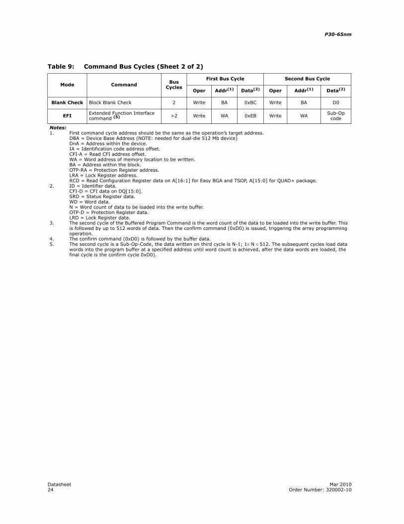
Datasheet Mar 201024 Order Number: 320002-10
Blank Check Block Blank Check 2 Write BA 0xBC Write BA D0
EFI Extended Function Interface command (5) >2 Write WA 0xEB Write WA Sub-Op
code
Notes:1. First command cycle address should be the same as the operation’s target address.
DBA = Device Base Address (NOTE: needed for dual-die 512 Mb device)DnA = Address within the device.IA = Identification code address offset.CFI-A = Read CFI address offset.WA = Word address of memory location to be written.BA = Address within the block.OTP-RA = Protection Register address.LRA = Lock Register address.RCD = Read Configuration Register data on A[16:1] for Easy BGA and TSOP, A[15:0] for QUAD+ package.
2. ID = Identifier data.CFI-D = CFI data on DQ[15:0].SRD = Status Register data.WD = Word data.N = Word count of data to be loaded into the write buffer.OTP-D = Protection Register data.LRD = Lock Register data.
3. The second cycle of the Buffered Program Command is the word count of the data to be loaded into the write buffer. This is followed by up to 512 words of data. Then the confirm command (0xD0) is issued, triggering the array programming operation.
4. The confirm command (0xD0) is followed by the buffer data.5. The second cycle is a Sub-Op-Code, the data written on third cycle is N-1; 1≤ N ≤ 512. The subsequent cycles load data
words into the program buffer at a specified address until word count is achieved, after the data words are loaded, the final cycle is the confirm cycle 0xD0).
Table 9: Command Bus Cycles (Sheet 2 of 2)
Mode Command BusCycles
First Bus Cycle Second Bus Cycle
Oper Addr(1) Data(2) Oper Addr(1) Data(2)
Datasheet Mar 201025 Order Number: 320002-10
P30-65nm
7.0 Read Operation
The device supports two read modes: asynchronous page mode and synchronous burst mode. Asynchronous page mode is the default read mode after device power-up or a reset. The Read Configuration Register must be configured to enable synchronous burst reads of the flash memory array (see Section 11.2, “Read Configuration Register” on page 39).
The device can be in any of four read states: Read Array, Read Identifier, Read Status or Read CFI. Upon power-up, or after a reset, the device defaults to Read Array. To change the read state, the appropriate read command must be written to the device (see Section 6.0, “Command Set” on page 21).
7.1 Asynchronous Page-Mode Read
Following a device power-up or reset, asynchronous page mode is the default read mode and the device is set to Read Array. However, to perform array reads after any other device operation (e.g. write operation), the Read Array command must be issued in order to read from the flash memory array.
Asynchronous page-mode reads can only be performed when Read Configuration Register bit RCR.15 is set (see Section 11.2, “Read Configuration Register” on page 39).
To perform an asynchronous page-mode read, an address is driven onto the Address bus, and CE# and ADV# are asserted. WE# and RST# must already have been deasserted. WAIT is deasserted during asynchronous page mode. ADV# can be driven high to latch the address, or it must be held low throughout the read cycle. CLK is not used for asynchronous page-mode reads, and is ignored. If only asynchronous reads are to be performed, CLK should be tied to a valid VIH level, WAIT signal can be floated and ADV# must be tied to ground. Array data is driven onto DQ[15:0] after an initial access time tAVQV delay. (see Section 15.0, “AC Characteristics” on page 53).
In asynchronous page mode, sixteen data words are “sensed” simultaneously from the flash memory array and loaded into an internal page buffer. The buffer word corresponding to the initial address on the Address bus is driven onto DQ[15:0] after the initial access delay. The lowest four address bits determine which word of the 16-word page is output from the data buffer at any given time.
7.2 Synchronous Burst-Mode Read
To perform a synchronous burst-read, an initial address is driven onto the Address bus, and CE# and ADV# are asserted. WE# and RST# must already have been deasserted. ADV# is asserted, and then deasserted to latch the address. Alternately, ADV# can remain asserted throughout the burst access, in which case the address is latched on the next valid CLK edge while ADV# is asserted.
During synchronous array and non-array read modes, the first word is output from the data buffer on the next valid CLK edge after the initial access latency delay (see Section 11.2.2, “Latency Count” on page 40). Subsequent data is output on valid CLK edges following a minimum delay. However, for a synchronous non-array read, the same word of data will be output on successive clock edges until the burst length requirements are satisfied. Refer to the following waveforms for more detailed information:
• Figure 24, “Synchronous Single-Word Array or Non-array Read Timing” on page 57
• Figure 25, “Continuous Burst Read, Showing An Output Delay Timing” on page 58
• Figure 26, “Synchronous Burst-Mode Four-Word Read Timing” on page 58
P30-65nm
Datasheet Mar 201026 Order Number: 320002-10
7.3 Read Device Identifier
The Read Device Identifier command instructs the device to output manufacturer code, device identifier code, block-lock status, protection register data, or configuration register data.
7.4 Read CFI
The Read CFI command instructs the device to output Common Flash Interface (CFI) data when read. See Section 6.0, “Command Set” on page 21 for details on issuing the Read CFI command. Appendix A, “Common Flash Interface Tables” on page 66 shows CFI information and address offsets within the CFI database.
Table 10: Device Identifier Information
Item Address(1) Data
Manufacturer Code 0x00 0x89h
Device ID Code 0x01 ID (see Table 11, “Device ID codes”)
Block Lock Configuration:
BBA(1) + 0x02
Lock Bit:
• Block Is Unlocked DQ0 = 0b0
• Block Is Locked DQ0 = 0b1
• Block Is not Locked-Down DQ1 = 0b0
• Block Is Locked-Down DQ1 = 0b1
Read Configuration Register 0x05 RCR Contents
General Purpose Register(3) DBA(2) + 0x07 GPR Data
Lock Register 0 0x80 PR-LK0 data
64-bit Factory-Programmed OTP Register 0x81–0x84 Factory OTP Register Data
64-bit User-Programmable OTP Register 0x85–0x88 User OTP Register Data
Lock Register 1 0x89 PR-LK1 OTP register lock data
128-bit User-Programmable Protection Registers 0x8A–0x109 OTP Register Data
Notes:1. BBA = Block Base Address.2. DBA = Device base Address, Numonyx reserves other configuration address locations.3. The GPR is used as read out register for Extended Function interface command.
Table 11: Device ID codes
ID Code Type Device Density
Device Identifier Codes
–T(Top Parameter)
–B(Bottom Parameter)
Device Code 256-Mbit 8919 891C
Note: The 512-Mbit devices do not have a unique Device ID associated with them. Each die within the stack can be identified by either of the 256-Mbit Device ID codes depending on its parameter option.
Datasheet Mar 201027 Order Number: 320002-10
P30-65nm
8.0 Program Operation
The device supports three programming methods: Word Programming (40h or 10h), Buffered Programming (E8h, D0h), and Buffered Enhanced Factory Programming (80h, D0h). See Section 5.0, “Bus Operations” on page 19 for details on the various programming commands issued to the device. The following sections describe device programming in detail.
Successful programming requires the addressed block to be unlocked. If the block is locked down, WP# must be deasserted and the block must be unlocked before attempting to program the block. Attempting to program a locked block causes a program error (SR.4 and SR.1 set) and termination of the operation. See Section 10.0, “Security Modes” on page 35 for details on locking and unlocking blocks.
8.1 Word Programming
Word programming operations are initiated by writing the Word Program Setup command to the device (see Section 5.0, “Bus Operations” on page 19). This is followed by a second write to the device with the address and data to be programmed. The device outputs Status Register data when read. See Figure 35, “Word Program Flowchart” on page 78. VPP must be above VPPLK, and within the specified VPPL min/max values.
During programming, the Write State Machine (WSM) executes a sequence of internally-timed events that program the desired data bits at the addressed location, and verifies that the bits are sufficiently programmed. Programming the flash memory array changes “ones” to “zeros”. Memory array bits that are zeros can be changed to ones only by erasing the block (see Section 9.0, “Erase Operations” on page 33).
The Status Register can be examined for programming progress and errors by reading at any address. The device remains in the Read Status Register state until another command is written to the device.
Status Register bit SR.7 indicates the programming status while the sequence executes. Commands that can be issued to the device during programming are Program Suspend, Read Status Register, Read Device Identifier, Read CFI, and Read Array (this returns unknown data).
When programming has finished, Status Register bit SR.4 (when set) indicates a programming failure. If SR.3 is set, the WSM could not perform the word programming operation because VPP was outside of its acceptable limits. If SR.1 is set, the word programming operation attempted to program a locked block, causing the operation to abort.
Before issuing a new command, the Status Register contents should be examined and then cleared using the Clear Status Register command. Any valid command can follow, when word programming has completed.
8.2 Buffered Programming
The device features a 512-word buffer to enable optimum programming performance. For Buffered Programming, data is first written to an on-chip write buffer. Then the buffer data is programmed into the flash memory array in buffer-size increments. This can improve system programming performance significantly over non-buffered programming.
P30-65nm
Datasheet Mar 201028 Order Number: 320002-10
When the Buffered Programming Setup command is issued (see Section 6.0, “Command Set” on page 21), Status Register information is updated and reflects the availability of the buffer. SR.7 indicates buffer availability: if set, the buffer is available; if cleared, the buffer is not available.
Note: The device default state is to output SR data after the Buffer Programming Setup Command. CE# and OE# low drive device to update Status Register. It is not allowed to issue 70h to read SR data after E8h command otherwise 70h would be counted as Word Count.
On the next write, a word count is written to the device at the buffer address. This tells the device how many data words will be written to the buffer, up to the maximum size of the buffer.
On the next write, a device start address is given along with the first data to be written to the flash memory array. Subsequent writes provide additional device addresses and data. All data addresses must lie within the start address plus the word count. Optimum programming performance and lower power usage are obtained by aligning the starting address at the beginning of a 512-word boundary (A[9:1] = 0x00 for Easy BGA and TSOP, A[8:0] for QUAD+ package). The maximum buffer size would be 256-word if the misaligned address range is crossing a 512-word boundary during programming.
After the last data is written to the buffer, the Buffered Programming Confirm command must be issued to the original block address. The WSM begins to program buffer contents to the flash memory array. If a command other than the Buffered Programming Confirm command is written to the device, a command sequence error occurs and Status Register bits SR[7,5,4] are set. If an error occurs while writing to the array, the device stops programming, and Status Register bits SR[7,4] are set, indicating a programming failure.
When Buffered Programming has completed, additional buffer writes can be initiated by issuing another Buffered Programming Setup command and repeating the buffered program sequence. Buffered programming may be performed with VPP = VPPL or VPPH (see Section 13.2, “Operating Conditions” on page 50 for limitations when operating the device with VPP = VPPH).
If an attempt is made to program past an erase-block boundary using the Buffered Program command, the device aborts the operation. This generates a command sequence error, and Status Register bits SR[5,4] are set.
If Buffered programming is attempted while VPP is at or below VPPLK, Status Register bits SR[4,3] are set. If any errors are detected that have set Status Register bits, the Status Register should be cleared using the Clear Status Register command.
8.3 Buffered Enhanced Factory Programming
Buffered Enhanced Factory Programing (BEFP) speeds up Multi-Level Cell (MLC) flash programming. The enhanced programming algorithm used in BEFP eliminates traditional programming elements that drive up overhead in device programmer systems.
BEFP consists of three phases: Setup, Program/Verify, and Exit (see Figure 38, “BEFP Flowchart” on page 81). It uses a write buffer to spread MLC program performance across 512 data words. Verification occurs in the same phase as programming to accurately program the flash memory cell to the correct bit state.
Datasheet Mar 201029 Order Number: 320002-10
P30-65nm
A single two-cycle command sequence programs the entire block of data. This enhancement eliminates three write cycles per buffer: two commands and the word count for each set of 512 data words. Host programmer bus cycles fill the device’s write buffer followed by a status check. SR.0 indicates when data from the buffer has been programmed into sequential flash memory array locations.
Following the buffer-to-flash array programming sequence, the Write State Machine (WSM) increments internal addressing to automatically select the next 512-word array boundary. This aspect of BEFP saves host programming equipment the address-bus setup overhead.
With adequate continuity testing, programming equipment can rely on the WSM’s internal verification to ensure that the device has programmed properly. This eliminates the external post-program verification and its associated overhead.
8.3.1 BEFP Requirements and Considerations
Note: Word buffer boundaries in the array are determined by A[9:1] for Easy BGA and TSOP, A[8:0] for QUAD+ package (0x000 through 0x1FF). The alignment start point is A[9:1] = 0x000 for Easy BGA and TSOP, A[8:0] = 0x000 for QUAD+ package.
Note:1. Some degradation in performance may occur if this limit is exceeded, but the internal algorithm continues to work
properly.2. If the internal address counter increments beyond the block's maximum address, addressing wraps around to the
beginning of the block.3. If the number of words is less than 512, remaining locations must be filled with 0xFFFF.
8.3.2 BEFP Setup Phase
After receiving the BEFP Setup and Confirm command sequence, Status Register bit SR.7 (Ready) is cleared, indicating that the WSM is busy with BEFP algorithm startup. A delay before checking SR.7 is required to allow the WSM enough time to perform all of
Table 12: BEFP Requirements
Parameter/Issue Requirement Notes
Case Temperature TC = 30°C ± 10 °C
VCC Nominal Vcc
VPP Driven to VPPH
Setup and Confirm Target block must be unlocked before issuing the BEFP Setup and Confirm commands
ProgrammingThe first-word address (WA0) of the block to be programmed must be held constant from the setup phase through all data streaming into the target block, until transition to the exit phase is desired
Buffer Alignment WA0 must align with the start of an array buffer boundary 1
Table 13: BEFP Considerations
Parameter/Issue Requirement Notes
Cycling For optimum performance, cycling must be limited below 50 erase cycles per block. 1
Programming blocks BEFP programs one block at a time; all buffer data must fall within a single block 2
Suspend BEFP cannot be suspended
Programming the flash memory array Programming to the flash memory array can occur only when the buffer is full. 3

P30-65nm
Datasheet Mar 201030 Order Number: 320002-10
its setups and checks (Block-Lock status, VPP level, etc.). If an error is detected, SR.4 is set and BEFP operation terminates. If the block was found to be locked, SR.1 is also set. SR.3 is set if the error occurred due to an incorrect VPP level.
Note: Reading from the device after the BEFP Setup and Confirm command sequence outputs Status Register data. Do not issue the Read Status Register command; it will be interpreted as data to be loaded into the buffer.
8.3.3 BEFP Program/Verify Phase
After the BEFP Setup Phase has completed, the host programming system must check SR[7,0] to determine the availability of the write buffer for data streaming. SR.7 cleared indicates the device is busy and the BEFP program/verify phase is activated. SR.0 indicates the write buffer is available.
Two basic sequences repeat in this phase: loading of the write buffer, followed by buffer data programming to the array. For BEFP, the count value for buffer loading is always the maximum buffer size of 512 words. During the buffer-loading sequence, data is stored to sequential buffer locations starting at address 0x00. Programming of the buffer contents to the flash memory array starts as soon as the buffer is full. If the number of words is less than 512, the remaining buffer locations must be filled with 0xFFFF.
Caution: The buffer must be completely filled for programming to occur. Supplying an address outside of the current block's range during a buffer-fill sequence causes the algorithm to exit immediately. Any data previously loaded into the buffer during the fill cycle is not programmed into the array.
The starting address for data entry must be buffer size aligned, if not the BEFP algorithm will be aborted and the program fails and (SR.4) flag will be set.
Data words from the write buffer are directed to sequential memory locations in the flash memory array; programming continues from where the previous buffer sequence ended. The host programming system must poll SR.0 to determine when the buffer program sequence completes. SR.0 cleared indicates that all buffer data has been transferred to the flash array; SR.0 set indicates that the buffer is not available yet for the next fill cycle. The host system may check full status for errors at any time, but it is only necessary on a block basis after BEFP exit. After the buffer fill cycle, no write cycles should be issued to the device until SR.0 = 0 and the device is ready for the next buffer fill.
Note: Any spurious writes are ignored after a buffer fill operation and when internal program is proceeding.
The host programming system continues the BEFP algorithm by providing the next group of data words to be written to the buffer. Alternatively, it can terminate this phase by changing the block address to one outside of the current block’s range.
The Program/Verify phase concludes when the programmer writes to a different block address; data supplied must be 0xFFFF. Upon Program/Verify phase completion, the device enters the BEFP Exit phase.
8.3.4 BEFP Exit Phase
When SR.7 is set, the device has returned to normal operating conditions. A full status check should be performed at this time to ensure the entire block programmed successfully. When exiting the BEFP algorithm with a block address change, the read mode will not change. After BEFP exit, any valid command can be issued to the device.
Datasheet Mar 201031 Order Number: 320002-10
P30-65nm
8.4 Program Suspend
Issuing the Program Suspend command while programming suspends the programming operation. This allows data to be accessed from the device other than the one being programmed. The Program Suspend command can be issued to any device address. A program operation can be suspended to perform reads only. Additionally, a program operation that is running during an erase suspend can be suspended to perform a read operation (see Figure 36, “Program Suspend/Resume Flowchart” on page 79).
When a programming operation is executing, issuing the Program Suspend command requests the WSM to suspend the programming algorithm at predetermined points. The device continues to output Status Register data after the Program Suspend command is issued. Programming is suspended when Status Register bits SR[7,2] are set. Suspend latency is specified in Section 16.0, “Program and Erase Characteristics” on page 63.
To read data from the device, the Read Array command must be issued. Read Array, Read Status Register, Read Device Identifier, Read CFI, and Program Resume are valid commands during a program suspend.
During a program suspend, deasserting CE# places the device in standby, reducing active current. VPP must remain at its programming level, and WP# must remain unchanged while in program suspend. If RST# is asserted, the device is reset.
8.5 Program Resume
The Resume command instructs the device to continue programming, and automatically clears Status Register bits SR[7,2]. This command can be written to any address. If error bits are set, the Status Register should be cleared before issuing the next instruction. RST# must remain deasserted (see Figure 36, “Program Suspend/Resume Flowchart” on page 79).
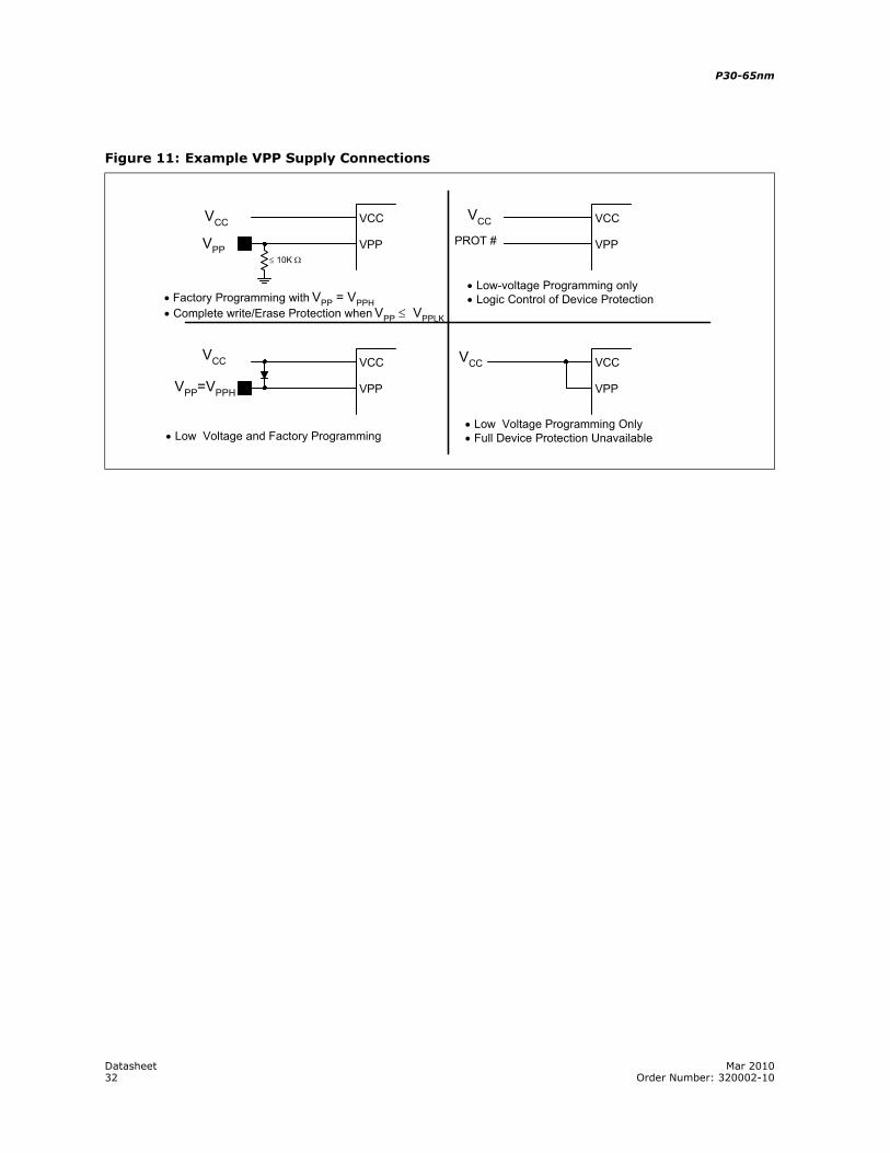
8.6 Program Protection
When VPP = VIL, absolute hardware write protection is provided for all device blocks. If VPP is at or below VPPLK, programming operations halt and SR.3 is set indicating a VPP-level error. Block lock registers are not affected by the voltage level on VPP; they may still be programmed and read, even if VPP is less than VPPLK.
P30-65nm
Datasheet Mar 201032 Order Number: 320002-10
Figure 11: Example VPP Supply Connections
• Factory Programming with VPP = VPPH• Complete write/Erase Protection when VPP ≤ VPPLK
VCC
VPP
VCC
VPP
• Low Voltage and Factory Programming
• Low-voltage Programming only• Logic Control of Device Protection
VCC
VPP
• Low Voltage Programming Only• Full Device Protection Unavailable
VCC
VPP
≤ 10K Ω
VPP
VCC VCC
PROT #
VCC
VPP=VPPH
VCC
Datasheet Mar 201033 Order Number: 320002-10
P30-65nm
9.0 Erase Operations
Flash erasing is performed on a block basis. An entire block is erased each time an erase command sequence is issued, and only one block is erased at a time. When a block is erased, all bits within that block read as logical ones. The following sections describe block erase operations in detail.
9.1 Block Erase
Block erase operations are initiated by writing the Block Erase Setup command to the address of the block to be erased (see Section 6.0, “Command Set” on page 21). Next, the Block Erase Confirm command is written to the address of the block to be erased. If the device is placed in standby (CE# deasserted) during an erase operation, the device completes the erase operation before entering standby.VPP must be above VPPLK and the block must be unlocked (see Figure 39, “Block Erase Flowchart” on page 82).
During a block erase, the Write State Machine (WSM) executes a sequence of internally-timed events that conditions, erases, and verifies all bits within the block. Erasing the flash memory array changes “zeros” to “ones”. Memory block array that are ones can be changed to zeros only by programming the block (see Section 8.0, “Program Operation” on page 27).
The Status Register can be examined for block erase progress and errors by reading any address. The device remains in the Read Status Register state until another command is written. SR.0 indicates whether the addressed block is erasing. Status Register bit SR.7 is set upon erase completion.
Status Register bit SR.7 indicates block erase status while the sequence executes. When the erase operation has finished, Status Register bit SR.5 indicates an erase failure if set. SR.3 set would indicate that the WSM could not perform the erase operation because VPP was outside of its acceptable limits. SR.1 set indicates that the erase operation attempted to erase a locked block, causing the operation to abort.
Before issuing a new command, the Status Register contents should be examined and then cleared using the Clear Status Register command. Any valid command can follow once the block erase operation has completed.
9.2 Blank Check
The Blank Check operation determines whether a specified main block is blank (i.e. completely erased). Without Blank Check, Block Erase would be the only other way to ensure a block is completely erased. Blank Check is especially useful in the case of erase operation interrupted by a power loss event.
Blank check can apply to only one block at a time, and no operations other than StatusRegister Reads are allowed during Blank Check (e.g. reading array data, program,erase etc). Suspend and resume operations are not supported during Blank Check, nor is Blank Check supported during any suspended operations.
Blank Check operations are initiated by writing the Blank Check Setup command to the block address. Next, the Check Confirm command is issued along with the same block address. When a successful command sequence is entered, the device automatically enters the Read Status State. The WSM then reads the entire specified block, and determines whether any bit in the block is programmed or over-erased.
P30-65nm
Datasheet Mar 201034 Order Number: 320002-10
The status register can be examined for Blank Check progress and errors by reading any address within the block being accessed. During a blank check operation, the Status Register indicates a busy status (SR.7 = 0). Upon completion, the Status Register indicates a ready status (SR.7 = 1). The Status Register should be checked for any errors, and then cleared. If the Blank Check operation fails, which means the block is not completely erased, the Status Register bit SR.5 will be set (“1”). CE# or OE# toggle (during polling) updates the Status Register.
After examining the Status Register, it should be cleared by the Clear Status Register command before issuing a new command. The device remains in Status Register Mode until another command is written to the device. Any command can follow once the Blank Check command is complete.
9.3 Erase Suspend
Issuing the Erase Suspend command while erasing suspends the block erase operation. This allows data to be accessed from memory locations other than the one being erased. The Erase Suspend command can be issued to any device address. A block erase operation can be suspended to perform a word or buffer program operation, or a read operation within any block except the block that is erase suspended (see Figure 40, “Erase Suspend/Resume Flowchart” on page 83).
When a block erase operation is executing, issuing the Erase Suspend command requests the WSM to suspend the erase algorithm at predetermined points. The device continues to output Status Register data after the Erase Suspend command is issued. Block erase is suspended when Status Register bits SR[7,6] are set. Suspend latency is specified in Section 16.0, “Program and Erase Characteristics” on page 63.
To read data from the device (other than an erase-suspended block), the Read Array command must be issued. During Erase Suspend, a Program command can be issued to any block other than the erase-suspended block. Block erase cannot resume until program operations initiated during erase suspend complete. Read Array, Read Status Register, Read Device Identifier, Read CFI, and Erase Resume are valid commands during Erase Suspend. Additionally, Clear Status Register, Program, Program Suspend, Block Lock, Block Unlock, and Block Lock-Down are valid commands during Erase Suspend.
During an erase suspend, deasserting CE# places the device in standby, reducing active current. VPP must remain at a valid level, and WP# must remain unchanged while in erase suspend. If RST# is asserted, the device is reset.
9.4 Erase Resume
The Erase Resume command instructs the device to continue erasing, and automatically clears status register bits SR[7,6]. This command can be written to any address. If status register error bits are set, the Status Register should be cleared before issuing the next instruction. RST# must remain deasserted (see Figure 40, “Erase Suspend/Resume Flowchart” on page 83).
9.5 Erase Protection
When VPP = VIL, absolute hardware erase protection is provided for all device blocks. If VPP is at or below VPPLK, erase operations halt and SR.3 is set indicating a VPP-level error.
Datasheet Mar 201035 Order Number: 320002-10
P30-65nm
10.0 Security Modes
The device features security modes used to protect the information stored in the flash memory array. The following sections describe each security mode in detail.
10.1 Block Locking
Individual instant block locking is used to protect user code and/or data within the flash memory array. All blocks power-up in a locked state to protect array data from being altered during power transitions. Any block can be locked or unlocked with no latency. Locked blocks cannot be programmed or erased; they can only be read.
Software-controlled security is implemented using the Block Lock and Block Unlock commands. Hardware-controlled security can be implemented using the Block Lock-Down command along with asserting WP#. Also, VPP data security can be used to inhibit program and erase operations (see Section 8.6, “Program Protection” on page 31 and Section 9.5, “Erase Protection” on page 34).
10.1.1 Lock Block
To lock a block, issue the Block Lock Setup command, followed by the Block Lock command issued to the desired block’s address. If the Set Read Configuration Register command is issued after the Block Lock Setup command, the device configures the RCR instead.
Block lock and unlock operations are not affected by the voltage level on VPP. The block lock bits may be modified and/or read even if VPP is at or below VPPLK.
10.1.2 Unlock Block
The Block Unlock command is used to unlock blocks (see Section 6.0, “Command Set” on page 21). Unlocked blocks can be read, programmed, and erased. Unlocked blocks return to a locked state when the device is reset or powered down. If a block is in a lock-down state, WP# must be deasserted before it can be unlocked (see Figure 12, “Block Locking State Diagram” on page 36).
10.1.3 Lock-Down Block
A locked or unlocked block can be locked-down by writing the Block Lock-Down command sequence (see Section 6.0, “Command Set” on page 21). Blocks in a lock-down state cannot be programmed or erased; they can only be read. However, unlike locked blocks, their locked state cannot be changed by software commands alone. A locked-down block can only be unlocked by issuing the Block Unlock command with WP# deasserted. To return an unlocked block to locked-down state, a Block Lock-Down command must be issued prior to changing WP# to VIL. Locked-down blocks revert to the locked state upon reset or power up the device (see Figure 12, “Block Locking State Diagram” on page 36).
10.1.4 Block Lock Status
The Read Device Identifier command is used to determine a block’s lock status (see Section 12.0, “Power and Reset Specifications” on page 48). Data bits DQ[1:0] display the addressed block’s lock status; DQ0 is the addressed block’s lock bit, while DQ1 is the addressed block’s lock-down bit.
P30-65nm
Datasheet Mar 201036 Order Number: 320002-10
Note: LK: Lock Setup Command, 60h; LK/D0h: Unlock Command; LK/01h: Lock Command; LK/2Fh: Lock-Down Command.
10.1.5 Block Locking During Suspend
Block lock and unlock changes can be performed during an erase suspend. To change block locking during an erase operation, first issue the Erase Suspend command. Monitor the Status Register until SR.7 and SR.6 are set, indicating the device is suspended and ready to accept another command.
Next, write the desired lock command sequence to a block, which changes the lock state of that block. After completing block lock or unlock operations, resume the erase operation using the Erase Resume command.
Note: A Lock Block Setup command followed by any command other than Lock Block, Unlock Block, or Lock-Down Block produces a command sequence error and set Status Register bits SR.4 and SR.5. If a command sequence error occurs during an erase suspend, SR.4 and SR.5 remains set, even after the erase operation is resumed. Unless the Status Register is cleared using the Clear Status Register command before resuming the erase operation, possible erase errors may be masked by the command sequence error.
If a block is locked or locked-down during an erase suspend of the same block, the lock status bits change immediately. However, the erase operation completes when it is resumed. Block lock operations cannot occur during a program suspend. See Appendix A, “Write State Machine” on page 87, which shows valid commands during an erase suspend.
Figure 12: Block Locking State Diagram
[0 0 0 ] [0 0 1 ]
[0 1 1 ]
[1 1 1 ]
[1 0 1 ]
[1 1 0 ]
[1 0 0 ]
L K /D 0 h
L K /0 1 h
L K /2 F h
L K /2 F h
L K /D 0 h
L K /0 1 h o r 2 F h
L K /D 0 h
L K /0 1 h
L K /2 F h L K /
2 F h
P G M /E R A S E A L L O W E D
P G M /E R A S E P R E V E N T E D
W P # = V IL = 0
W P # = V IH = 1
P o w e r -U p /R e s e t D e fa u lt
P o w e r -U p /R e s e t D e fa u lt
L o c k e d -d o w n
L o c k e d -d o w nis d is a b le d b y
W P # = V IH
V ir tu a l lo c k -d o w n
A n y L o c kc o m m a n d s
W P # to g g le
W P # tog g le
[0 1 0 ]
Datasheet Mar 201037 Order Number: 320002-10
P30-65nm
10.2 Selectable One-Time Programmable Blocks
The OTP security feature on P30-65nm device is backward compatible to the P30-130nm device. Please see your local Numonyx representative for details about its implementation.
10.3 Password Access
The Password Access is a security enhancement offered on the P30-65nm device. This feature protects information stored in array blocks by preventing content alteration or reads until a valid 64-bit password is received. The Password Access may be combined with Non-Volatile Protection and/or Volatile Protection to create a multi-tiered solution.
Please contact your Numonyx Sales for further details concerning Password Access.
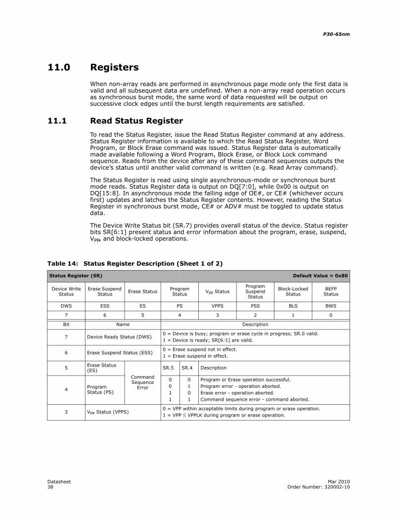
P30-65nm
Datasheet Mar 201038 Order Number: 320002-10
11.0 Registers
When non-array reads are performed in asynchronous page mode only the first data is valid and all subsequent data are undefined. When a non-array read operation occurs as synchronous burst mode, the same word of data requested will be output on successive clock edges until the burst length requirements are satisfied.
11.1 Read Status Register
To read the Status Register, issue the Read Status Register command at any address. Status Register information is available to which the Read Status Register, Word Program, or Block Erase command was issued. Status Register data is automatically made available following a Word Program, Block Erase, or Block Lock command sequence. Reads from the device after any of these command sequences outputs the device’s status until another valid command is written (e.g. Read Array command).
The Status Register is read using single asynchronous-mode or synchronous burst mode reads. Status Register data is output on DQ[7:0], while 0x00 is output on DQ[15:8]. In asynchronous mode the falling edge of OE#, or CE# (whichever occurs first) updates and latches the Status Register contents. However, reading the Status Register in synchronous burst mode, CE# or ADV# must be toggled to update status data.
The Device Write Status bit (SR.7) provides overall status of the device. Status register bits SR[6:1] present status and error information about the program, erase, suspend, VPP, and block-locked operations.
Table 14: Status Register Description (Sheet 1 of 2)
Status Register (SR) Default Value = 0x80
Device Write Status
Erase Suspend Status Erase Status Program
Status VPP StatusProgram Suspend Status
Block-Locked Status
BEFP Status
DWS ESS ES PS VPPS PSS BLS BWS
7 6 5 4 3 2 1 0
Bit Name Description
7 Device Ready Status (DWS)0 = Device is busy; program or erase cycle in progress; SR.0 valid.1 = Device is ready; SR[6:1] are valid.
6 Erase Suspend Status (ESS)0 = Erase suspend not in effect.1 = Erase suspend in effect.
5 Erase Status (ES)
Command Sequence
Error
SR.5 SR.4 Description
4 Program Status (PS)
0011
0101
Program or Erase operation successful.Program error - operation aborted.Erase error - operation aborted.Command sequence error - command aborted.
3 VPP Status (VPPS)0 = VPP within acceptable limits during program or erase operation.1 = VPP ≤ VPPLK during program or erase operation.
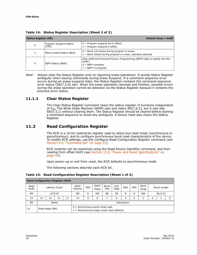
Datasheet Mar 201039 Order Number: 320002-10
P30-65nm
Note: Always clear the Status Register prior to resuming erase operations. It avoids Status Register ambiguity when issuing commands during Erase Suspend. If a command sequence error occurs during an erase-suspend state, the Status Register contains the command sequence error status (SR[7,5,4] set). When the erase operation resumes and finishes, possible errors during the erase operation cannot be detected via the Status Register because it contains the previous error status.
11.1.1 Clear Status Register
The Clear Status Register command clears the status register. It functions independent of VPP. The Write State Machine (WSM) sets and clears SR[7,6,2], but it sets bits SR[5:3,1] without clearing them. The Status Register should be cleared before starting a command sequence to avoid any ambiguity. A device reset also clears the Status Register.
11.2 Read Configuration Register
The RCR is a 16-bit read/write register used to select bus-read mode (synchronous or asynchronous), and to configure synchronous burst read characteristics of the device. To modify RCR settings, use the Configure Read Configuration Register command (see Section 6.0, “Command Set” on page 21).
RCR contents can be examined using the Read Device Identifier command, and then reading from offset 0x05 (see Section 12.0, “Power and Reset Specifications” on page 48).
Upon power-up or exit from reset, the RCR defaults to asynchronous mode.
The following sections describe each RCR bit.
2 Program Suspend Status (PSS)
0 = Program suspend not in effect.1 = Program suspend in effect.
1 Block-Locked Status (BLS)0 = Block not locked during program or erase.1 = Block locked during program or erase; operation aborted.
0 BEFP Status (BWS)
After Buffered Enhanced Factory Programming (BEFP) data is loaded into the buffer:0 = BEFP complete.1 = BEFP in-progress.
Table 14: Status Register Description (Sheet 2 of 2)
Status Register (SR) Default Value = 0x80
Table 15: Read Configuration Register Description (Sheet 1 of 2)
Read Configuration Register (RCR)
Read Mode Latency Count WAIT
Polarity RESWAITDelay
Burst Seq
CLK Edge RES RES
BurstWrap
Burst Length
RM LC[3:0] WP R WD BS CE R R BW BL[2:0]
15 14 13 12 11 10 9 8 7 6 5 4 3 2 1 0
Bit Name Description
15 Read Mode (RM)0 = Synchronous burst-mode read1 = Asynchronous page-mode read (default)
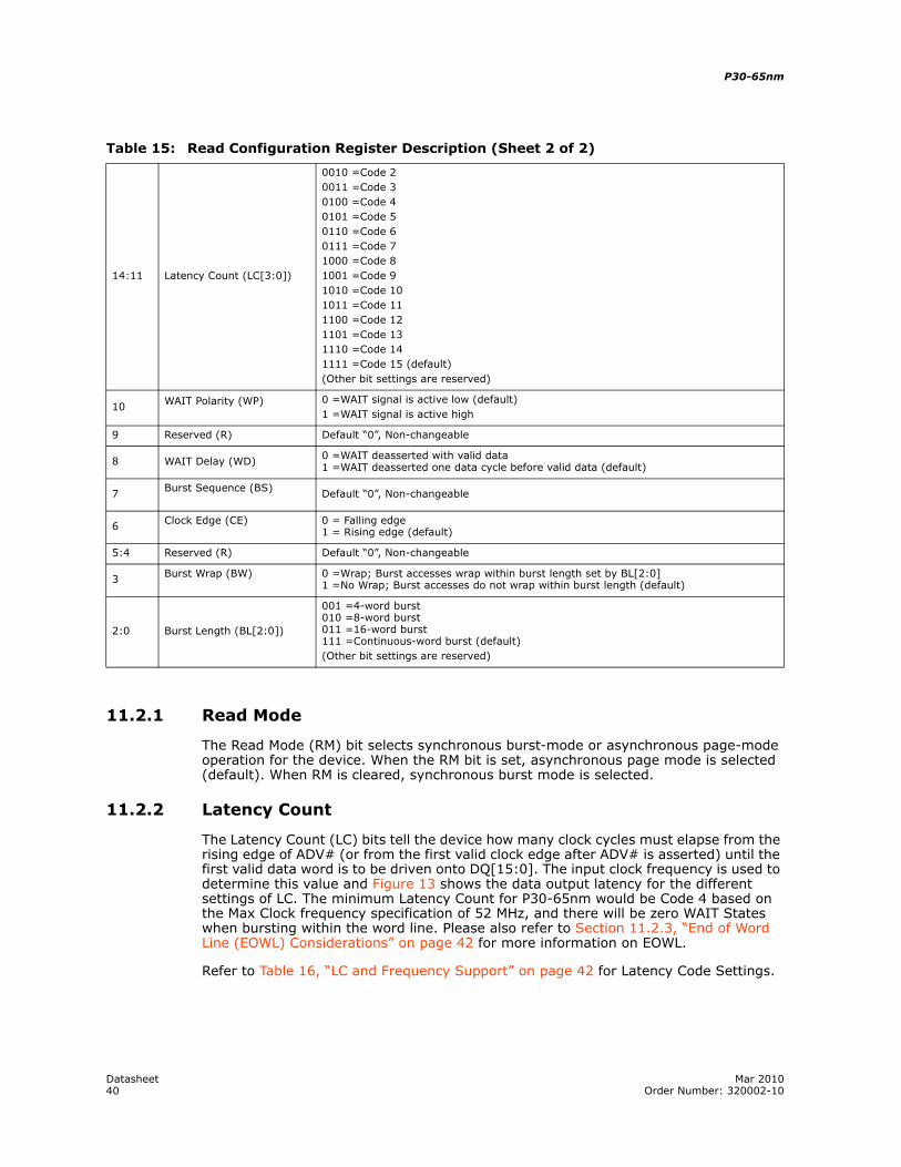
P30-65nm
Datasheet Mar 201040 Order Number: 320002-10
11.2.1 Read Mode
The Read Mode (RM) bit selects synchronous burst-mode or asynchronous page-mode operation for the device. When the RM bit is set, asynchronous page mode is selected (default). When RM is cleared, synchronous burst mode is selected.
11.2.2 Latency Count
The Latency Count (LC) bits tell the device how many clock cycles must elapse from the rising edge of ADV# (or from the first valid clock edge after ADV# is asserted) until the first valid data word is to be driven onto DQ[15:0]. The input clock frequency is used to determine this value and Figure 13 shows the data output latency for the different settings of LC. The minimum Latency Count for P30-65nm would be Code 4 based on the Max Clock frequency specification of 52 MHz, and there will be zero WAIT States when bursting within the word line. Please also refer to Section 11.2.3, “End of Word Line (EOWL) Considerations” on page 42 for more information on EOWL.
Refer to Table 16, “LC and Frequency Support” on page 42 for Latency Code Settings.
14:11 Latency Count (LC[3:0])
0010 =Code 20011 =Code 30100 =Code 40101 =Code 50110 =Code 60111 =Code 71000 =Code 81001 =Code 91010 =Code 101011 =Code 111100 =Code 121101 =Code 131110 =Code 141111 =Code 15 (default)(Other bit settings are reserved)
10 WAIT Polarity (WP) 0 =WAIT signal is active low (default)1 =WAIT signal is active high
9 Reserved (R) Default “0”, Non-changeable
8 WAIT Delay (WD) 0 =WAIT deasserted with valid data1 =WAIT deasserted one data cycle before valid data (default)
7 Burst Sequence (BS) Default “0”, Non-changeable
6 Clock Edge (CE) 0 = Falling edge1 = Rising edge (default)
5:4 Reserved (R) Default “0”, Non-changeable
3 Burst Wrap (BW) 0 =Wrap; Burst accesses wrap within burst length set by BL[2:0]1 =No Wrap; Burst accesses do not wrap within burst length (default)
2:0 Burst Length (BL[2:0])
001 =4-word burst010 =8-word burst011 =16-word burst111 =Continuous-word burst (default)(Other bit settings are reserved)
Table 15: Read Configuration Register Description (Sheet 2 of 2)
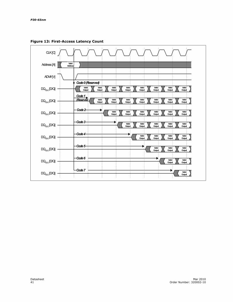
Datasheet Mar 201041 Order Number: 320002-10
P30-65nm
Figure 13: First-Access Latency Count
Code 1(Reserved
Code 6
Code 5
Code 4
Code 3
Code 2
Code 0 (Reserved)
Code 7
ValidAddress
ValidOutput
ValidOutput
ValidOutput
ValidOutput
ValidOutput
ValidOutput
ValidOutput
ValidOutput
ValidOutput
ValidOutput
ValidOutput
ValidOutput
ValidOutput
ValidOutput
ValidOutput
ValidOutput
ValidOutput
ValidOutput
ValidOutput
ValidOutput
ValidOutput
ValidOutput
ValidOutput
ValidOutput
ValidOutput
ValidOutput
ValidOutput
ValidOutput
ValidOutput
ValidOutput
ValidOutput
ValidOutput
ValidOutput
ValidOutput
ValidOutput
ValidOutput
Address [A]
ADV# [V]
DQ15-0 [D/Q]
CLK [C]
DQ15-0 [D/Q]
DQ15-0 [D/Q]
DQ15-0 [D/Q]
DQ15-0 [D/Q]
DQ15-0 [D/Q]
DQ15-0 [D/Q]
DQ15-0 [D/Q]
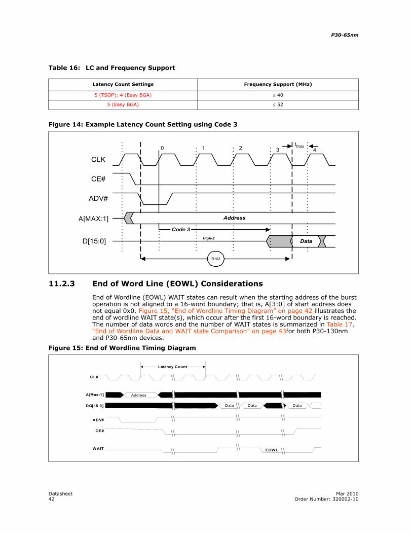
P30-65nm
Datasheet Mar 201042 Order Number: 320002-10
Table 16: LC and Frequency Support
11.2.3 End of Word Line (EOWL) Considerations
End of Wordline (EOWL) WAIT states can result when the starting address of the burst operation is not aligned to a 16-word boundary; that is, A[3:0] of start address does not equal 0x0. Figure 15, “End of Wordline Timing Diagram” on page 42 illustrates the end of wordline WAIT state(s), which occur after the first 16-word boundary is reached. The number of data words and the number of WAIT states is summarized in Table 17, “End of Wordline Data and WAIT state Comparison” on page 43for both P30-130nm and P30-65nm devices.
Latency Count Settings Frequency Support (MHz)
5 (TSOP); 4 (Easy BGA) ≤ 40
5 (Easy BGA) ≤ 52
Figure 14: Example Latency Count Setting using Code 3
CLK
CE#
ADV#
A[MAX:0]
D[15:0]
tData
Code 3
Address
Data
0 1 2 3 4
R103
High-Z
A[MAX:1]
Figure 15: End of Wordline Timing Diagram
A[Max:1]
ADV#
OE#
WAIT
DQ[15:0] Data Data Data
EOWL
CLK
Latency Count
Address

Datasheet Mar 201043 Order Number: 320002-10
P30-65nm
Table 17: End of Wordline Data and WAIT state Comparison
11.2.4 WAIT Polarity
The WAIT Polarity bit (WP), RCR.10 determines the asserted level (VOH or VOL) of WAIT. When WP is set, WAIT is asserted high (default). When WP is cleared, WAIT is asserted low. WAIT changes state on valid clock edges during active bus cycles (CE# asserted, OE# asserted, RST# deasserted).
11.2.4.1 WAIT Signal Function
The WAIT signal indicates data valid when the device is operating in synchronous mode (RCR.15 =0). The WAIT signal is only “deasserted” when data is valid on the bus.
When the device is operating in synchronous non-array read mode, such as read status, read ID, or read CFI. The WAIT signal is also “deasserted” when data is valid on the bus.
WAIT behavior during synchronous non-array reads at the end of word line works correctly only on the first data access.
When the device is operating in asynchronous page mode, asynchronous single word read mode, and all write operations, WAIT is set to a deasserted state as determined by RCR.10. See Figure 22, “Asynchronous Single-Word Read (ADV# Latch)” on page 56, and Figure 23, “Asynchronous Page-Mode Read Timing” on page 57.
Latency CountP30-130nm P30-65nm
Data States WAIT States Data States WAIT States
1 Not Supported Not Supported Not Supported Not Supported2 4 0 to 1 Not Supported Not Supported3 4 0 to 2 16 0 to 24 4 0 to 3 16 0 to 35 4 0 to 4 16 0 to 46 4 0 to 5 16 0 to 57 4 0 to 6 16 0 to 68
Not Supported Not Supported
16 0 to 79 16 0 to 810 16 0 to 911 16 0 to 1012 16 0 to 1113 16 0 to 1214 16 0 to 1315 16 0 to 14
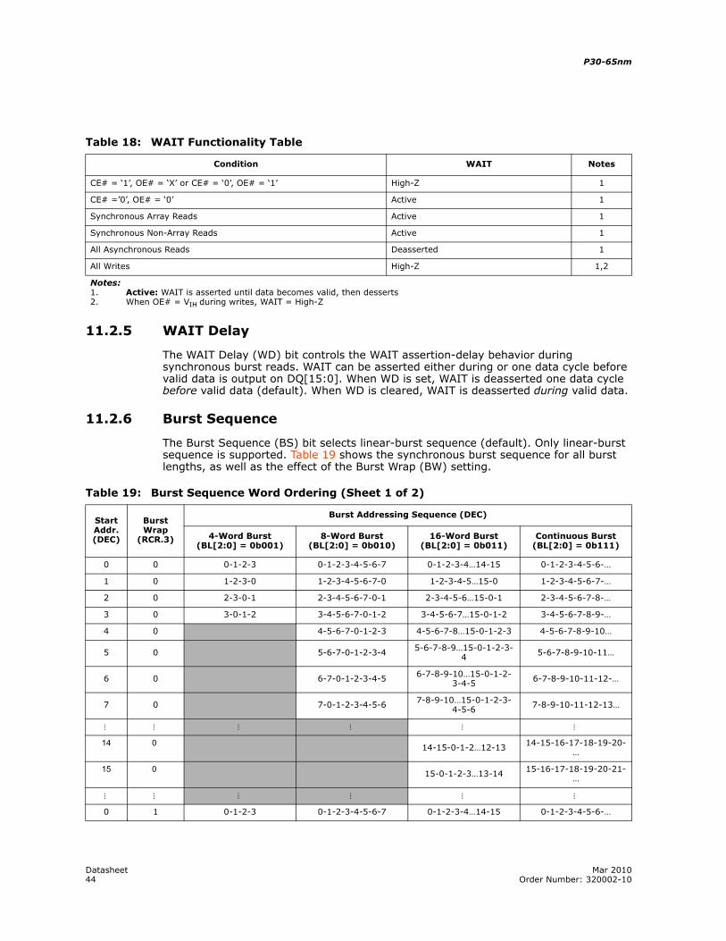
P30-65nm
Datasheet Mar 201044 Order Number: 320002-10
11.2.5 WAIT Delay
The WAIT Delay (WD) bit controls the WAIT assertion-delay behavior during synchronous burst reads. WAIT can be asserted either during or one data cycle before valid data is output on DQ[15:0]. When WD is set, WAIT is deasserted one data cycle before valid data (default). When WD is cleared, WAIT is deasserted during valid data.
11.2.6 Burst Sequence
The Burst Sequence (BS) bit selects linear-burst sequence (default). Only linear-burst sequence is supported. Table 19 shows the synchronous burst sequence for all burst lengths, as well as the effect of the Burst Wrap (BW) setting.
Table 18: WAIT Functionality Table
Condition WAIT Notes
CE# = ‘1’, OE# = ‘X’ or CE# = ‘0’, OE# = ‘1’ High-Z 1
CE# =’0’, OE# = ‘0’ Active 1
Synchronous Array Reads Active 1
Synchronous Non-Array Reads Active 1
All Asynchronous Reads Deasserted 1
All Writes High-Z 1,2
Notes:1. Active: WAIT is asserted until data becomes valid, then desserts2. When OE# = VIH during writes, WAIT = High-Z
Table 19: Burst Sequence Word Ordering (Sheet 1 of 2)
StartAddr.(DEC)
Burst Wrap
(RCR.3)
Burst Addressing Sequence (DEC)
4-Word Burst(BL[2:0] = 0b001)
8-Word Burst(BL[2:0] = 0b010)
16-Word Burst(BL[2:0] = 0b011)
Continuous Burst(BL[2:0] = 0b111)
0 0 0-1-2-3 0-1-2-3-4-5-6-7 0-1-2-3-4…14-15 0-1-2-3-4-5-6-…
1 0 1-2-3-0 1-2-3-4-5-6-7-0 1-2-3-4-5…15-0 1-2-3-4-5-6-7-…
2 0 2-3-0-1 2-3-4-5-6-7-0-1 2-3-4-5-6…15-0-1 2-3-4-5-6-7-8-…
3 0 3-0-1-2 3-4-5-6-7-0-1-2 3-4-5-6-7…15-0-1-2 3-4-5-6-7-8-9-…
4 0 4-5-6-7-0-1-2-3 4-5-6-7-8…15-0-1-2-3 4-5-6-7-8-9-10…
5 0 5-6-7-0-1-2-3-4 5-6-7-8-9…15-0-1-2-3-4 5-6-7-8-9-10-11…
6 0 6-7-0-1-2-3-4-5 6-7-8-9-10…15-0-1-2-3-4-5 6-7-8-9-10-11-12-…
7 0 7-0-1-2-3-4-5-6 7-8-9-10…15-0-1-2-3-4-5-6 7-8-9-10-11-12-13…
… … … … … …
14 0 14-15-0-1-2…12-13 14-15-16-17-18-19-20-…
15 0 15-0-1-2-3…13-14 15-16-17-18-19-20-21-…
… … … … … …
0 1 0-1-2-3 0-1-2-3-4-5-6-7 0-1-2-3-4…14-15 0-1-2-3-4-5-6-…
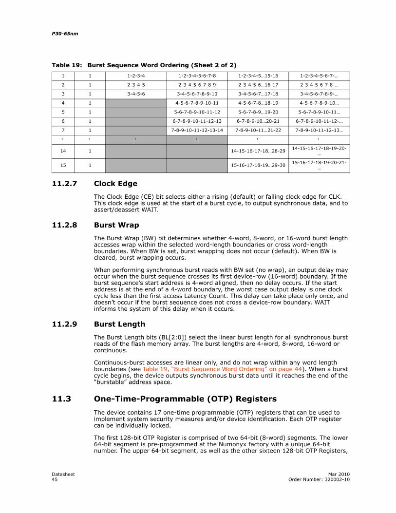
Datasheet Mar 201045 Order Number: 320002-10
P30-65nm
11.2.7 Clock Edge
The Clock Edge (CE) bit selects either a rising (default) or falling clock edge for CLK. This clock edge is used at the start of a burst cycle, to output synchronous data, and to assert/deassert WAIT.
11.2.8 Burst Wrap
The Burst Wrap (BW) bit determines whether 4-word, 8-word, or 16-word burst length accesses wrap within the selected word-length boundaries or cross word-length boundaries. When BW is set, burst wrapping does not occur (default). When BW is cleared, burst wrapping occurs.
When performing synchronous burst reads with BW set (no wrap), an output delay may occur when the burst sequence crosses its first device-row (16-word) boundary. If the burst sequence’s start address is 4-word aligned, then no delay occurs. If the start address is at the end of a 4-word boundary, the worst case output delay is one clock cycle less than the first access Latency Count. This delay can take place only once, and doesn’t occur if the burst sequence does not cross a device-row boundary. WAIT informs the system of this delay when it occurs.
11.2.9 Burst Length
The Burst Length bits (BL[2:0]) select the linear burst length for all synchronous burst reads of the flash memory array. The burst lengths are 4-word, 8-word, 16-word or continuous.
Continuous-burst accesses are linear only, and do not wrap within any word length boundaries (see Table 19, “Burst Sequence Word Ordering” on page 44). When a burst cycle begins, the device outputs synchronous burst data until it reaches the end of the “burstable” address space.
11.3 One-Time-Programmable (OTP) Registers
The device contains 17 one-time programmable (OTP) registers that can be used to implement system security measures and/or device identification. Each OTP register can be individually locked.
The first 128-bit OTP Register is comprised of two 64-bit (8-word) segments. The lower 64-bit segment is pre-programmed at the Numonyx factory with a unique 64-bit number. The upper 64-bit segment, as well as the other sixteen 128-bit OTP Registers,
1 1 1-2-3-4 1-2-3-4-5-6-7-8 1-2-3-4-5…15-16 1-2-3-4-5-6-7-…
2 1 2-3-4-5 2-3-4-5-6-7-8-9 2-3-4-5-6…16-17 2-3-4-5-6-7-8-…
3 1 3-4-5-6 3-4-5-6-7-8-9-10 3-4-5-6-7…17-18 3-4-5-6-7-8-9-…
4 1 4-5-6-7-8-9-10-11 4-5-6-7-8…18-19 4-5-6-7-8-9-10…
5 1 5-6-7-8-9-10-11-12 5-6-7-8-9…19-20 5-6-7-8-9-10-11…
6 1 6-7-8-9-10-11-12-13 6-7-8-9-10…20-21 6-7-8-9-10-11-12-…
7 1 7-8-9-10-11-12-13-14 7-8-9-10-11…21-22 7-8-9-10-11-12-13…
… … … … … …
14 1 14-15-16-17-18…28-29 14-15-16-17-18-19-20-…
15 1 15-16-17-18-19…29-30 15-16-17-18-19-20-21-…
Table 19: Burst Sequence Word Ordering (Sheet 2 of 2)

P30-65nm
Datasheet Mar 201046 Order Number: 320002-10
are blank. Users can program these registers as needed. Once programmed, users can then lock the OTP Register(s) to prevent additional bit programming (see Figure 16, “OTP Register Map” on page 46).
The OTP Registers contain one-time programmable (OTP) bits; when programmed, PR bits cannot be erased. Each OTP Register can be accessed multiple times to program individual bits, as long as the register remains unlocked.
Each OTP Register has an associated Lock Register bit. When a Lock Register bit is programmed, the associated OTP Register can only be read; it can no longer be programmed. Additionally, because the Lock Register bits themselves are OTP, when programmed, Lock Register bits cannot be erased. Therefore, when a OTP Register is locked, it cannot be unlocked.
.
11.3.1 Reading the OTP Registers
The OTP Registers can be read from OTP-RA address. To read the OTP Register, first issue the Read Device Identifier command at OTP-RA address to place the device in the Read Device Identifier state (see Section 6.0, “Command Set” on page 21). Next,
Figure 16: OTP Register Map
0x89Lock Register 1
15 14 13 12 11 10 9 8 7 6 5 4 3 2 1 0
0x102
0x109
0x8A
0x91
128-bit Protection Register 16(User-Programmable)
128-bit Protection Register 1(User-Programmable)
0x88
0x85
64-bit Segment(User-Programmable)
0x84
0x81
0x80Lock Register 0
64-bit Segment(Factory-Programmed)
15 14 13 12 11 10 9 8 7 6 5 4 3 2 1 0
128-Bit Protection Register 0
Datasheet Mar 201047 Order Number: 320002-10
P30-65nm
perform a read operation using the address offset corresponding to the register to be read. Table 10, “Device Identifier Information” on page 26 shows the address offsets of the OTP Registers and Lock Registers. PR data is read 16 bits at a time.
11.3.2 Programming the OTP Registers
To program an OTP Register, first issue the Program OTP Register command at the parameter’s base address plus the offset of the desired OTP Register location (see Section 6.0, “Command Set” on page 21). Next, write the desired OTP Register data to the same OTP Register address (see Figure 16, “OTP Register Map” on page 46).
The device programs the 64-bit and 128-bit user-programmable OTP Register data 16 bits at a time (see Figure 42, “Protection Register Programming Flowchart” on page 85). Issuing the Program OTP Register command outside of the OTP Register’s address space causes a program error (SR.4 set). Attempting to program a locked OTP Register causes a program error (SR.4 set) and a lock error (SR.1 set).
Note: When programming the OTP bits in the OTP registers for a Top Parameter Device, the following upper address bits must also be driven properly: A[Max:17] driven high (VIH) for TSOP and Easy BGA packages, and A[Max:16] driven high (VIH) for QUAD+ SCSP.
11.3.3 Locking the OTP Registers
Each OTP Register can be locked by programming its respective lock bit in the Lock Register. To lock a OTP Register, program the corresponding bit in the Lock Register by issuing the Program Lock Register command, followed by the desired Lock Register data (see Section 6.0, “Command Set” on page 21). The physical addresses of the Lock Registers are 0x80 for register 0 and 0x89 for register 1. These addresses are used when programming the lock registers (see Table 10, “Device Identifier Information” on page 26).
Bit 0 of Lock Register 0 is already programmed during the manufacturing process by Numonyx factory, locking the lower half segment of the first 128-bit OTP Register. Bit 1 of Lock Register 0 can be programmed by user to the upper half segment of the first 128-bit OTP Register. When programming Bit 1 of Lock Register 0, all other bits need to be left as ‘1’ such that the data programmed is 0xFFFD.
Lock Register 1 controls the locking of the upper sixteen 128-bit OTP Registers. Each bit of Lock Register 1 corresponds to a specific 128-bit OTP Register. Programming a bit in Lock Register 1 locks the corresponding 128-bit OTP Register; e.g., programming LR1.0 locks the corresponding OTP Register 1.
Caution: After being locked, the OTP Registers cannot be unlocked.
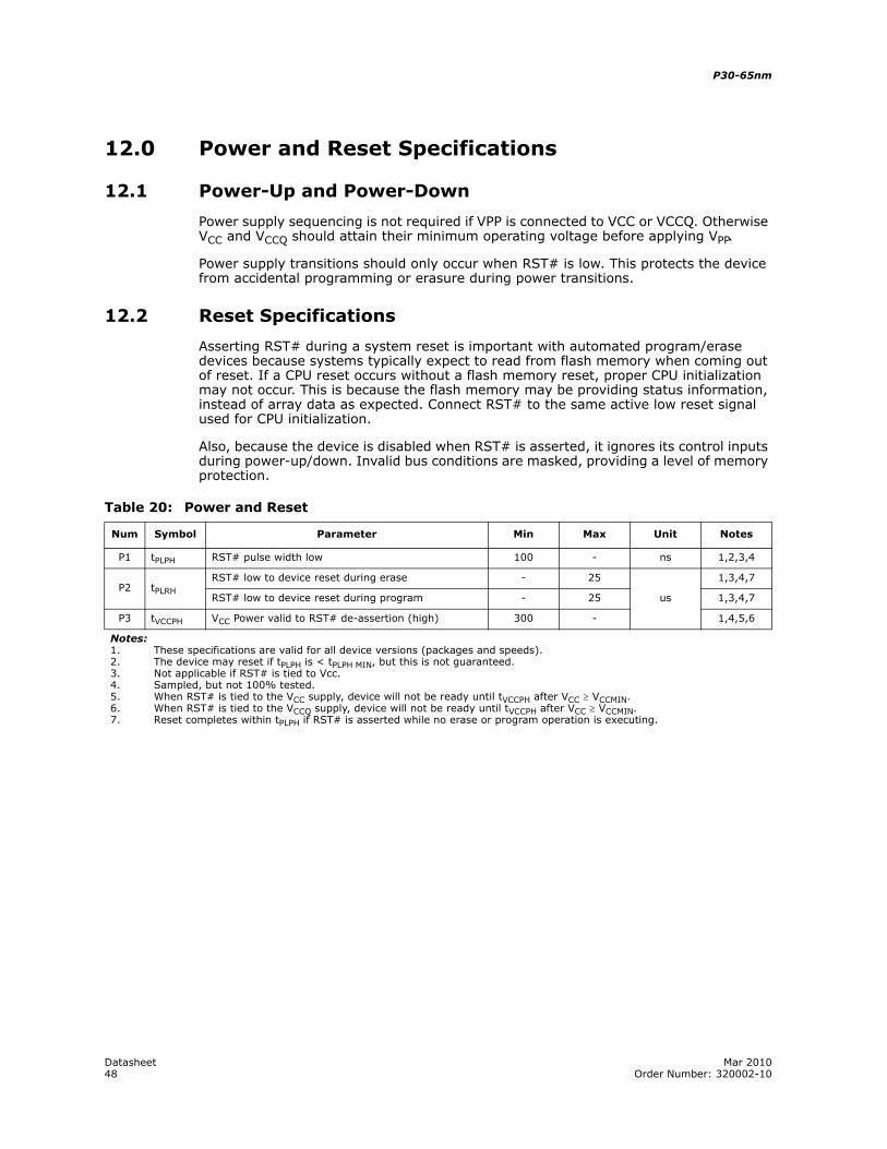
P30-65nm
Datasheet Mar 201048 Order Number: 320002-10
12.0 Power and Reset Specifications
12.1 Power-Up and Power-Down
Power supply sequencing is not required if VPP is connected to VCC or VCCQ. Otherwise VCC and VCCQ should attain their minimum operating voltage before applying VPP.
Power supply transitions should only occur when RST# is low. This protects the device from accidental programming or erasure during power transitions.
12.2 Reset Specifications
Asserting RST# during a system reset is important with automated program/erase devices because systems typically expect to read from flash memory when coming out of reset. If a CPU reset occurs without a flash memory reset, proper CPU initialization may not occur. This is because the flash memory may be providing status information, instead of array data as expected. Connect RST# to the same active low reset signal used for CPU initialization.
Also, because the device is disabled when RST# is asserted, it ignores its control inputs during power-up/down. Invalid bus conditions are masked, providing a level of memory protection.
Table 20: Power and Reset
Num Symbol Parameter Min Max Unit Notes
P1 tPLPH RST# pulse width low 100 - ns 1,2,3,4
P2 tPLRH
RST# low to device reset during erase - 25
us
1,3,4,7
RST# low to device reset during program - 25 1,3,4,7
P3 tVCCPH VCC Power valid to RST# de-assertion (high) 300 - 1,4,5,6
Notes:1. These specifications are valid for all device versions (packages and speeds).2. The device may reset if tPLPH is < tPLPH MIN, but this is not guaranteed.3. Not applicable if RST# is tied to Vcc.4. Sampled, but not 100% tested.5. When RST# is tied to the VCC supply, device will not be ready until tVCCPH after VCC ≥ VCCMIN. 6. When RST# is tied to the VCCQ supply, device will not be ready until tVCCPH after VCC ≥ VCCMIN.7. Reset completes within tPLPH if RST# is asserted while no erase or program operation is executing.
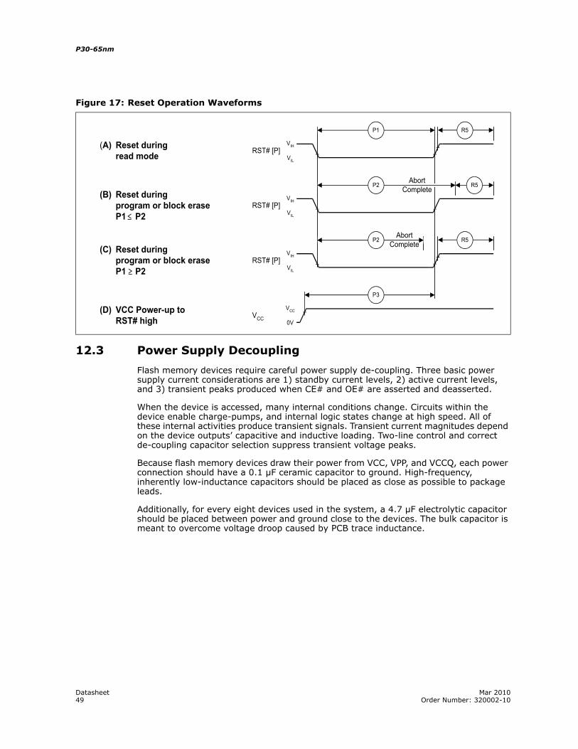
Datasheet Mar 201049 Order Number: 320002-10
P30-65nm
12.3 Power Supply Decoupling
Flash memory devices require careful power supply de-coupling. Three basic power supply current considerations are 1) standby current levels, 2) active current levels, and 3) transient peaks produced when CE# and OE# are asserted and deasserted.
When the device is accessed, many internal conditions change. Circuits within the device enable charge-pumps, and internal logic states change at high speed. All of these internal activities produce transient signals. Transient current magnitudes depend on the device outputs’ capacitive and inductive loading. Two-line control and correct de-coupling capacitor selection suppress transient voltage peaks.
Because flash memory devices draw their power from VCC, VPP, and VCCQ, each power connection should have a 0.1 µF ceramic capacitor to ground. High-frequency, inherently low-inductance capacitors should be placed as close as possible to package leads.
Additionally, for every eight devices used in the system, a 4.7 µF electrolytic capacitor should be placed between power and ground close to the devices. The bulk capacitor is meant to overcome voltage droop caused by PCB trace inductance.
Figure 17: Reset Operation Waveforms
(A) Reset duringread mode
(B) Reset duringprogram or block eraseP1 ≤ P2
(C) Reset duringprogram or block eraseP1 ≥ P2
VIH
VIL
VIH
VIL
VIH
VIL
RST# [P]
RST# [P]
RST# [P]
AbortComplete
AbortComplete
VCC
0VVCC
(D) VCC Power-up toRST# high
P1 R5
P2
P3
P2 R5
R5
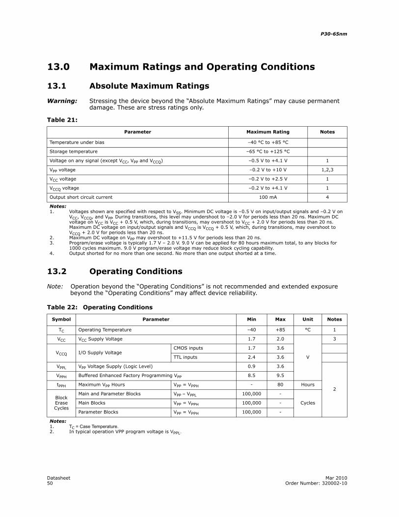
P30-65nm
Datasheet Mar 201050 Order Number: 320002-10
13.0 Maximum Ratings and Operating Conditions
13.1 Absolute Maximum Ratings
Warning: Stressing the device beyond the “Absolute Maximum Ratings” may cause permanent damage. These are stress ratings only.
13.2 Operating Conditions
Note: Operation beyond the “Operating Conditions” is not recommended and extended exposure beyond the “Operating Conditions” may affect device reliability.
Table 21:
Parameter Maximum Rating Notes
Temperature under bias –40 °C to +85 °C
Storage temperature –65 °C to +125 °C
Voltage on any signal (except VCC, VPP and VCCQ) –0.5 V to +4.1 V 1
VPP voltage –0.2 V to +10 V 1,2,3
VCC voltage –0.2 V to +2.5 V 1
VCCQ voltage –0.2 V to +4.1 V 1
Output short circuit current 100 mA 4
Notes:1. Voltages shown are specified with respect to VSS. Minimum DC voltage is –0.5 V on input/output signals and –0.2 V on
VCC, VCCQ, and VPP. During transitions, this level may undershoot to –2.0 V for periods less than 20 ns. Maximum DC voltage on VCC is VCC + 0.5 V, which, during transitions, may overshoot to VCC + 2.0 V for periods less than 20 ns. Maximum DC voltage on input/output signals and VCCQ is VCCQ + 0.5 V, which, during transitions, may overshoot to VCCQ + 2.0 V for periods less than 20 ns.
2. Maximum DC voltage on VPP may overshoot to +11.5 V for periods less than 20 ns.3. Program/erase voltage is typically 1.7 V – 2.0 V. 9.0 V can be applied for 80 hours maximum total, to any blocks for
1000 cycles maximum. 9.0 V program/erase voltage may reduce block cycling capability.4. Output shorted for no more than one second. No more than one output shorted at a time.
Table 22: Operating Conditions
Symbol Parameter Min Max Unit Notes
TC Operating Temperature –40 +85 °C 1
VCC VCC Supply Voltage 1.7 2.0
V
3
VCCQ I/O Supply VoltageCMOS inputs 1.7 3.6
TTL inputs 2.4 3.6
VPPL VPP Voltage Supply (Logic Level) 0.9 3.6
2
VPPH Buffered Enhanced Factory Programming VPP 8.5 9.5
tPPH Maximum VPP Hours VPP = VPPH - 80 Hours
Block Erase Cycles
Main and Parameter Blocks VPP = VPPL 100,000 -
CyclesMain Blocks VPP = VPPH 100,000 -
Parameter Blocks VPP = VPPH 100,000 -
Notes:1. TC = Case Temperature.2. In typical operation VPP program voltage is VPPL.
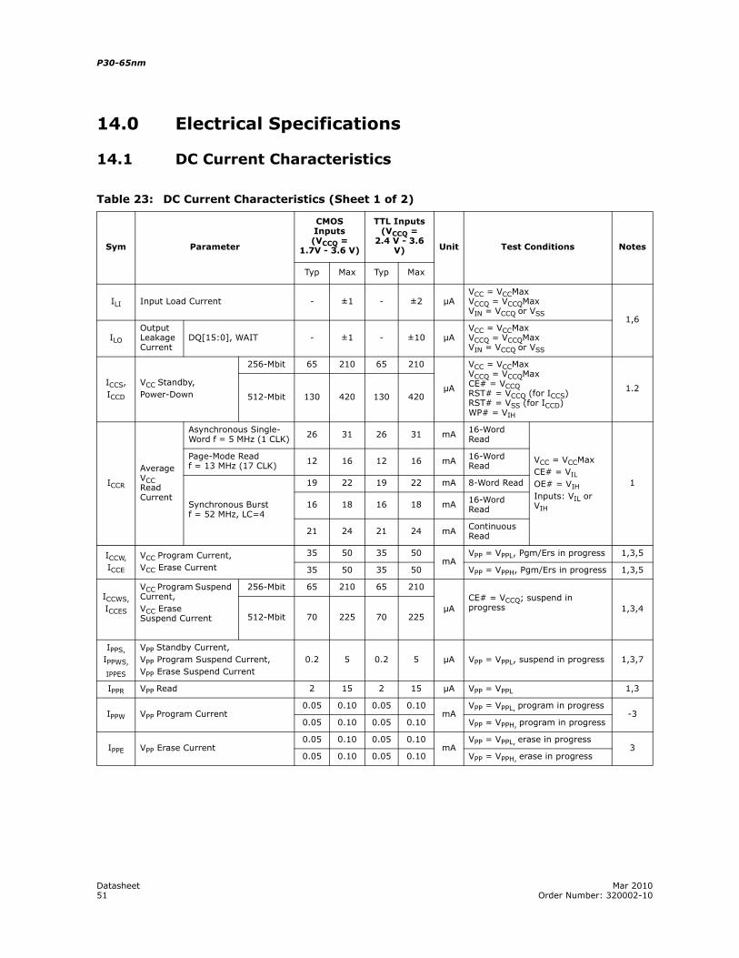
Datasheet Mar 201051 Order Number: 320002-10
P30-65nm
14.0 Electrical Specifications
14.1 DC Current Characteristics
Table 23: DC Current Characteristics (Sheet 1 of 2)
Sym Parameter
CMOS Inputs(VCCQ =
1.7V - 3.6 V)
TTL Inputs(VCCQ =
2.4 V - 3.6 V) Unit Test Conditions Notes
Typ Max Typ Max
ILI Input Load Current - ±1 - ±2 µAVCC = VCCMaxVCCQ = VCCQMaxVIN = VCCQ or VSS
1,6
ILO
Output Leakage Current
DQ[15:0], WAIT - ±1 - ±10 µAVCC = VCCMaxVCCQ = VCCQMaxVIN = VCCQ or VSS
ICCS,ICCD
VCC Standby,Power-Down
256-Mbit 65 210 65 210
µA
VCC = VCCMaxVCCQ = VCCQMax CE# = VCCQRST# = VCCQ (for ICCS)RST# = VSS (for ICCD)WP# = VIH
1.2512-Mbit 130 420 130 420
ICCR
Average VCC Read Current
Asynchronous Single-Word f = 5 MHz (1 CLK) 26 31 26 31 mA 16-Word
Read
VCC = VCCMaxCE# = VILOE# = VIHInputs: VIL or VIH
1
Page-Mode Readf = 13 MHz (17 CLK) 12 16 12 16 mA 16-Word
Read
Synchronous Burst f = 52 MHz, LC=4
19 22 19 22 mA 8-Word Read
16 18 16 18 mA 16-Word Read
21 24 21 24 mA Continuous Read
ICCW,ICCE
VCC Program Current, VCC Erase Current
35 50 35 50mA
VPP = VPPL, Pgm/Ers in progress 1,3,5
35 50 35 50 VPP = VPPH, Pgm/Ers in progress 1,3,5
ICCWS,ICCES
VCC Program Suspend Current,VCC Erase Suspend Current
256-Mbit 65 210 65 210
µACE# = VCCQ; suspend in progress 1,3,4
512-Mbit 70 225 70 225
IPPS,IPPWS,
IPPES
VPP Standby Current,VPP Program Suspend Current,VPP Erase Suspend Current
0.2 5 0.2 5 µA VPP = VPPL, suspend in progress 1,3,7
IPPR VPP Read 2 15 2 15 µA VPP = VPPL 1,3
IPPW VPP Program Current0.05 0.10 0.05 0.10
mAVPP = VPPL, program in progress
-30.05 0.10 0.05 0.10 VPP = VPPH, program in progress
IPPE VPP Erase Current0.05 0.10 0.05 0.10
mAVPP = VPPL, erase in progress
30.05 0.10 0.05 0.10 VPP = VPPH, erase in progress
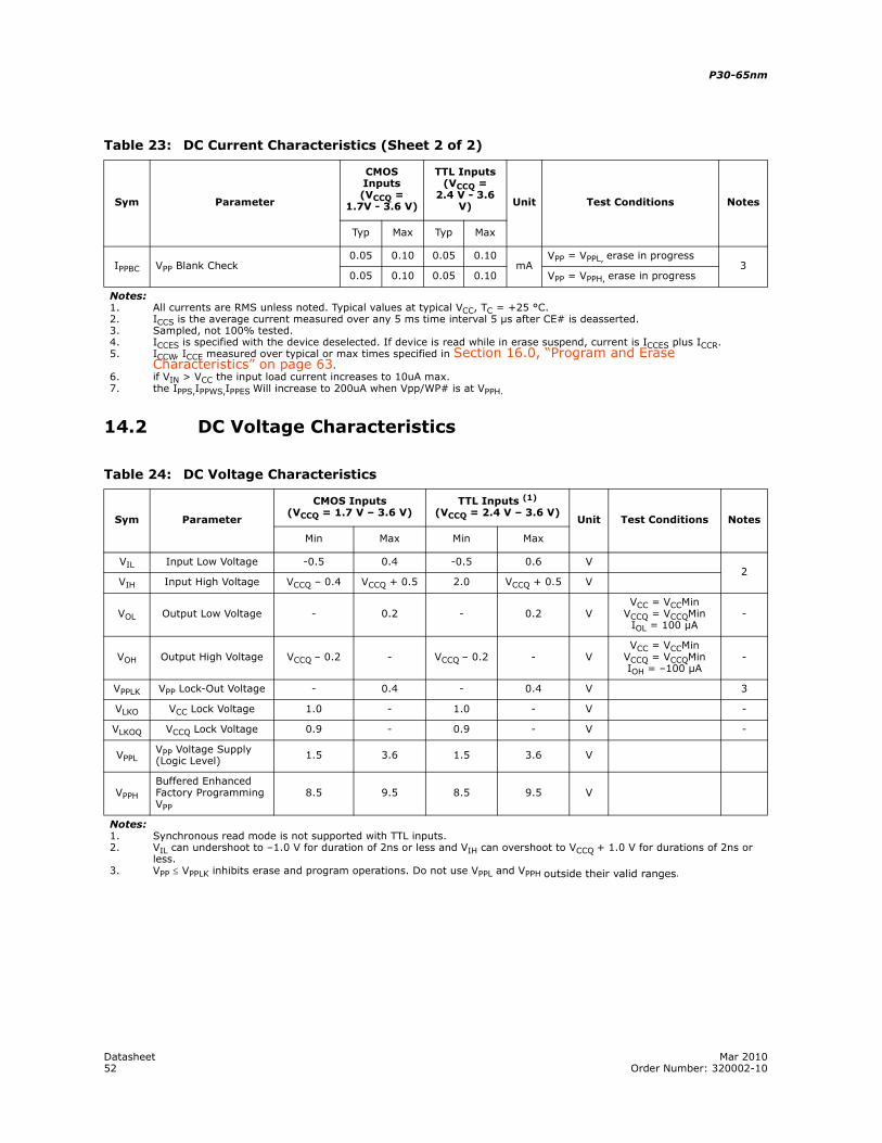
P30-65nm
Datasheet Mar 201052 Order Number: 320002-10
14.2 DC Voltage Characteristics
IPPBC VPP Blank Check0.05 0.10 0.05 0.10
mAVPP = VPPL, erase in progress
30.05 0.10 0.05 0.10 VPP = VPPH, erase in progress
Notes:1. All currents are RMS unless noted. Typical values at typical VCC, TC = +25 °C.2. ICCS is the average current measured over any 5 ms time interval 5 µs after CE# is deasserted.3. Sampled, not 100% tested.4. ICCES is specified with the device deselected. If device is read while in erase suspend, current is ICCES plus ICCR.5. ICCW, ICCE measured over typical or max times specified in Section 16.0, “Program and Erase
Characteristics” on page 63.6. if VIN > VCC the input load current increases to 10uA max.7. the IPPS,IPPWS,IPPES Will increase to 200uA when Vpp/WP# is at VPPH.
Table 24: DC Voltage Characteristics
Sym Parameter
CMOS Inputs (VCCQ = 1.7 V – 3.6 V)
TTL Inputs (1)
(VCCQ = 2.4 V – 3.6 V)Unit Test Conditions Notes
Min Max Min Max
VIL Input Low Voltage -0.5 0.4 -0.5 0.6 V2
VIH Input High Voltage VCCQ – 0.4 VCCQ + 0.5 2.0 VCCQ + 0.5 V
VOL Output Low Voltage - 0.2 - 0.2 VVCC = VCCMin
VCCQ = VCCQMinIOL = 100 µA
-
VOH Output High Voltage VCCQ – 0.2 - VCCQ – 0.2 - VVCC = VCCMin
VCCQ = VCCQMinIOH = –100 µA
-
VPPLK VPP Lock-Out Voltage - 0.4 - 0.4 V 3
VLKO VCC Lock Voltage 1.0 - 1.0 - V -
VLKOQ VCCQ Lock Voltage 0.9 - 0.9 - V -
VPPLVPP Voltage Supply (Logic Level) 1.5 3.6 1.5 3.6 V
VPPH
Buffered Enhanced Factory Programming VPP
8.5 9.5 8.5 9.5 V
Notes:1. Synchronous read mode is not supported with TTL inputs.2. VIL can undershoot to –1.0 V for duration of 2ns or less and VIH can overshoot to VCCQ + 1.0 V for durations of 2ns or
less.3. VPP ≤ VPPLK inhibits erase and program operations. Do not use VPPL and VPPH outside their valid ranges.
Table 23: DC Current Characteristics (Sheet 2 of 2)
Sym Parameter
CMOS Inputs(VCCQ =
1.7V - 3.6 V)
TTL Inputs(VCCQ =
2.4 V - 3.6 V) Unit Test Conditions Notes
Typ Max Typ Max
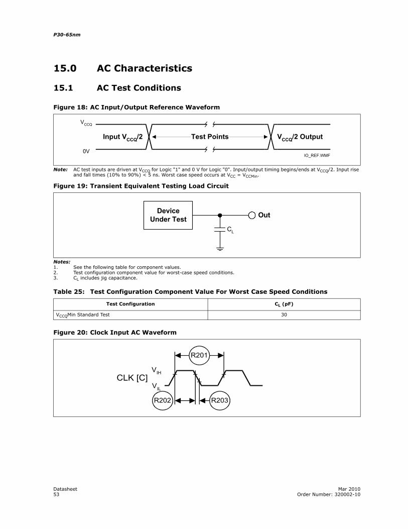
Datasheet Mar 201053 Order Number: 320002-10
P30-65nm
15.0 AC Characteristics
15.1 AC Test Conditions
Note: AC test inputs are driven at VCCQ for Logic "1" and 0 V for Logic "0". Input/output timing begins/ends at VCCQ/2. Input rise and fall times (10% to 90%) < 5 ns. Worst case speed occurs at VCC = VCCMin.
Notes:1. See the following table for component values.2. Test configuration component value for worst-case speed conditions.3. CL includes jig capacitance..
Figure 18: AC Input/Output Reference Waveform
Figure 19: Transient Equivalent Testing Load Circuit
Table 25: Test Configuration Component Value For Worst Case Speed Conditions
Test Configuration CL (pF)
VCCQMin Standard Test 30
Figure 20: Clock Input AC Waveform
IO_REF.WMF
Input VCCQ/2 VCCQ/2 Output
VCCQ
0V
Test Points
DeviceUnder Test Out
CL
CLK [C]VIH
VIL
R203R202
R201
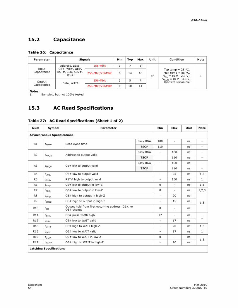
P30-65nm
Datasheet Mar 201054 Order Number: 320002-10
15.2 Capacitance
15.3 AC Read Specifications
Table 26: Capacitance
Parameter Signals Min Typ Max Unit Condition Note
Input Capacitance
Address, Data, CE#, WE#, OE#,
RST#, CLK, ADV#, WP#
256-Mbit 3 7 8
pF
Typ temp = 25 °C, Max temp = 85 °C, VCC = (0 V - 2.0 V), VCCQ = (0 V - 3.6 V), Discrete silicon die
1256-Mbit/256Mbit 6 14 16
Output Capacitance Data, WAIT
256-Mbit 3 5 7
256-Mbit/256Mbit 6 10 14
Notes:1. Sampled, but not 100% tested.
Table 27: AC Read Specifications (Sheet 1 of 2)
Num Symbol Parameter Min Max Unit Note
Asynchronous Specifications
R1 tAVAV Read cycle timeEasy BGA 100 - ns -
TSOP 110 ns -
R2 tAVQV Address to output validEasy BGA - 100 ns -
TSOP 110 ns -
R3 tELQV CE# low to output validEasy BGA - 100 ns -
TSOP 110 ns -
R4 tGLQV OE# low to output valid - 25 ns 1,2
R5 tPHQV RST# high to output valid - 150 ns 1
R6 tELQX CE# low to output in low-Z 0 - ns 1,3
R7 tGLQX OE# low to output in low-Z 0 - ns 1,2,3
R8 tEHQZ CE# high to output in high-Z - 20 ns
1,3R9 tGHQZ OE# high to output in high-Z - 15 ns
R10 tOHOutput hold from first occurring address, CE#, or OE# change 0 - ns
R11 tEHEL CE# pulse width high 17 - ns1
R12 tELTV CE# low to WAIT valid - 17 ns
R13 tEHTZ CE# high to WAIT high-Z - 20 ns 1,3
R15 tGLTV OE# low to WAIT valid - 17 ns 1
R16 tGLTX OE# low to WAIT in low-Z 0 - ns1,3
R17 tGHTZ OE# high to WAIT in high-Z - 20 ns
Latching Specifications
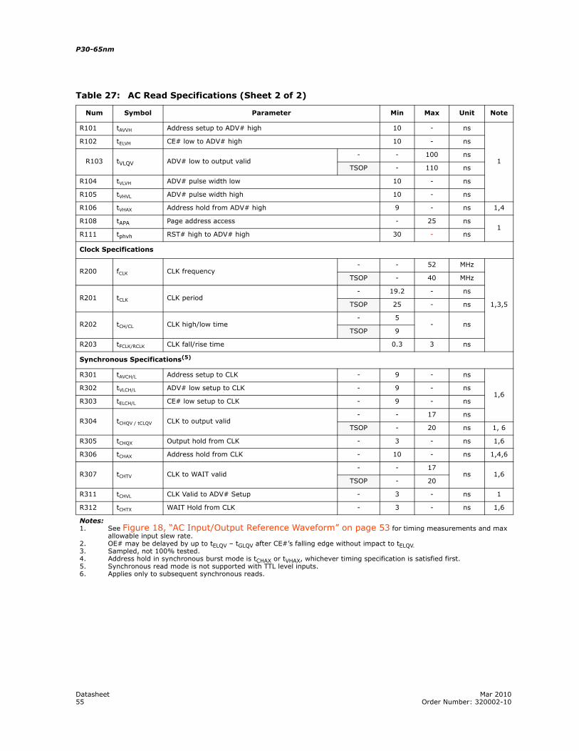
Datasheet Mar 201055 Order Number: 320002-10
P30-65nm
R101 tAVVH Address setup to ADV# high 10 - ns
1
R102 tELVH CE# low to ADV# high 10 - ns
R103 tVLQV ADV# low to output valid- - 100 ns
TSOP - 110 ns
R104 tVLVH ADV# pulse width low 10 - ns
R105 tVHVL ADV# pulse width high 10 - ns
R106 tVHAX Address hold from ADV# high 9 - ns 1,4
R108 tAPA Page address access - 25 ns1
R111 tphvh RST# high to ADV# high 30 - ns
Clock Specifications
R200 fCLK CLK frequency- - 52 MHz
1,3,5
TSOP - 40 MHz
R201 tCLK CLK period- 19.2 - ns
TSOP 25 - ns
R202 tCH/CL CLK high/low time- 5
- nsTSOP 9
R203 tFCLK/RCLK CLK fall/rise time 0.3 3 ns
Synchronous Specifications(5)
R301 tAVCH/L Address setup to CLK - 9 - ns
1,6R302 tVLCH/L ADV# low setup to CLK - 9 - ns
R303 tELCH/L CE# low setup to CLK - 9 - ns
R304 tCHQV / tCLQV CLK to output valid- - 17 ns
TSOP - 20 ns 1, 6
R305 tCHQX Output hold from CLK - 3 - ns 1,6
R306 tCHAX Address hold from CLK - 10 - ns 1,4,6
R307 tCHTV CLK to WAIT valid- - 17
ns 1,6TSOP - 20
R311 tCHVL CLK Valid to ADV# Setup - 3 - ns 1
R312 tCHTX WAIT Hold from CLK - 3 - ns 1,6
Notes:1. See Figure 18, “AC Input/Output Reference Waveform” on page 53 for timing measurements and max
allowable input slew rate.2. OE# may be delayed by up to tELQV – tGLQV after CE#’s falling edge without impact to tELQV.3. Sampled, not 100% tested.4. Address hold in synchronous burst mode is tCHAX or tVHAX, whichever timing specification is satisfied first.5. Synchronous read mode is not supported with TTL level inputs.6. Applies only to subsequent synchronous reads.
Table 27: AC Read Specifications (Sheet 2 of 2)
Num Symbol Parameter Min Max Unit Note
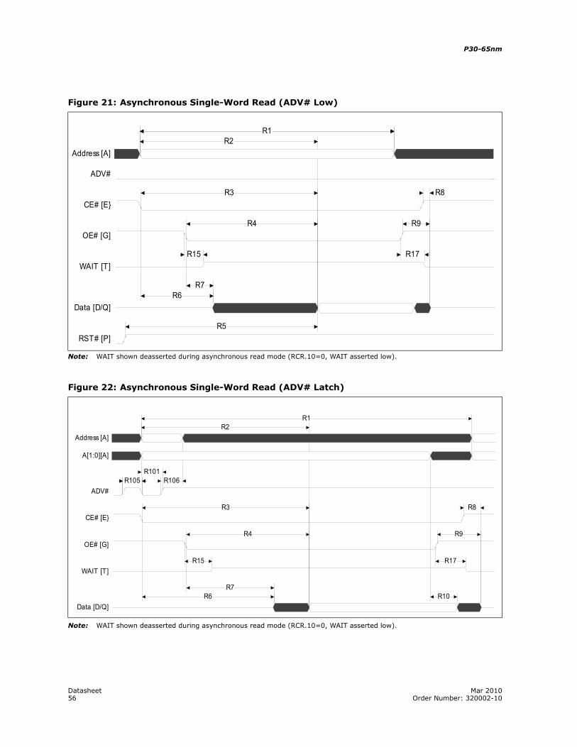
P30-65nm
Datasheet Mar 201056 Order Number: 320002-10
Note: WAIT shown deasserted during asynchronous read mode (RCR.10=0, WAIT asserted low).
Note: WAIT shown deasserted during asynchronous read mode (RCR.10=0, WAIT asserted low).
Figure 21: Asynchronous Single-Word Read (ADV# Low)
R5
R7R6
R17R15
R9R4
R8R3
R1R2
R1
Address [A]
ADV#
CE# [E}
OE# [G]
WAIT [T]
Data [D/Q]
RST# [P]
Figure 22: Asynchronous Single-Word Read (ADV# Latch)
R10R7
R6
R17R15
R9R4
R8R3
R106R101
R105R105
R2R1
Address [A]
A[1:0][A]
ADV#
CE# [E}
OE# [G]
WAIT [T]
Data [D/Q]
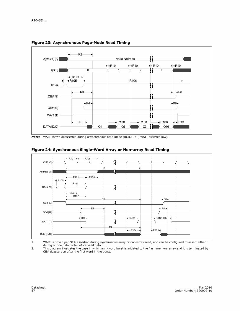
Datasheet Mar 201057 Order Number: 320002-10
P30-65nm
Note: WAIT shown deasserted during asynchronous read mode (RCR.10=0, WAIT asserted low).
1. WAIT is driven per OE# assertion during synchronous array or non-array read, and can be configured to assert either during or one data cycle before valid data.
2. This diagram illustrates the case in which an n-word burst is initiated to the flash memory array and it is terminated by CE# deassertion after the first word in the burst.
Figure 23: Asynchronous Page-Mode Read Timing
Valid Address
0 1 2 F
Q1 Q2 Q3 Q16R108R108R108 R13R6
R9R4
R8R3
R106R101
R105R105
R10R10R10R10
R2A[Max:4] [A]
A[3:0]
ADV#
CE# [E]
OE# [G]
WAIT [T]
DATA [D/Q]
Figure 24: Synchronous Single-Word Array or Non-array Read Timing
R312
R305R304R4
R17R307R15
R9R7
R8
R303R102
R3
R104
R106R101
R104R105R105
R2
R306R301CLK [C]
Address [A]
ADV# [V]
CE# [E]
OE# [G]
WAIT [T]
Data [D/Q]
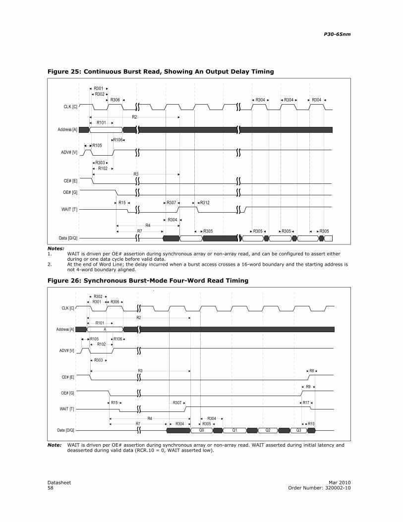
P30-65nm
Datasheet Mar 201058 Order Number: 320002-10
Notes:1. WAIT is driven per OE# assertion during synchronous array or non-array read, and can be configured to assert either
during or one data cycle before valid data.2. At the end of Word Line; the delay incurred when a burst access crosses a 16-word boundary and the starting address is
not 4-word boundary aligned.
Note: WAIT is driven per OE# assertion during synchronous array or non-array read. WAIT asserted during initial latency and deasserted during valid data (RCR.10 = 0, WAIT asserted low).
Figure 25: Continuous Burst Read, Showing An Output Delay Timing
Figure 26: Synchronous Burst-Mode Four-Word Read Timing
R305R305R305R305
R304R4
R7
R312R307R15
R303R102
R3
R106R105R105
R101R2
R304R304R304R306R302
R301
CLK [C]
Address [A]
ADV# [V]
CE# [E]
OE# [G]
WAIT [T]
Data [D/Q]
y
A
Q0 Q1 Q2 Q3
R307
R10R304
R305R304R4
R7
R17R15
R9
R8
R303
R3
R106R102
R105R105
R101R2
R306R302
R301CLK [C]
Address [A]
ADV# [V]
CE# [E]
OE# [G]
WAIT [T]
Data [D/Q]
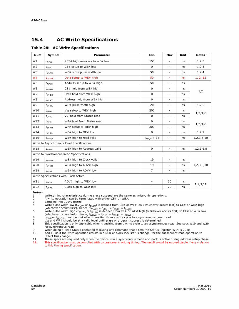
Datasheet Mar 201059 Order Number: 320002-10
P30-65nm
15.4 AC Write Specifications
Table 28: AC Write Specifications
Num Symbol Parameter Min Max Unit Notes
W1 tPHWL RST# high recovery to WE# low 150 - ns 1,2,3
W2 tELWL CE# setup to WE# low 0 - ns 1,2,3
W3 tWLWH WE# write pulse width low 50 - ns 1,2,4
W4 tDVWH Data setup to WE# high 50 - ns 1, 2, 12
W5 tAVWH Address setup to WE# high 50 - ns
1,2W6 tWHEH CE# hold from WE# high 0 - ns
W7 tWHDX Data hold from WE# high 0 - ns
W8 tWHAX Address hold from WE# high 0 - ns
W9 tWHWL WE# pulse width high 20 - ns 1,2,5
W10 tVPWH VPP setup to WE# high 200 - ns1,2,3,7
W11 tQVVL VPP hold from Status read 0 - ns
W12 tQVBL WP# hold from Status read 0 - ns1,2,3,7
W13 tBHWH WP# setup to WE# high 200 - ns
W14 tWHGL WE# high to OE# low 0 - ns 1,2,9
W16 tWHQV WE# high to read valid tAVQV + 35 - ns 1,2,3,6,10
Write to Asynchronous Read Specifications
W18 tWHAV WE# high to Address valid 0 - ns 1,2,3,6,8
Write to Synchronous Read Specifications
W19 tWHCH/L WE# high to Clock valid 19 - ns
1,2,3,6,10W20 tWHVH WE# high to ADV# high 19 - ns
W28 tWHVL WE# high to ADV# low 7 - ns
Write Specifications with Clock Active
W21 tVHWL ADV# high to WE# low - 20 ns1,2,3,11
W22 tCHWL Clock high to WE# low - 20 ns
Notes:1. Write timing characteristics during erase suspend are the same as write-only operations.2. A write operation can be terminated with either CE# or WE#.3. Sampled, not 100% tested. 4. Write pulse width low (tWLWH or tELEH) is defined from CE# or WE# low (whichever occurs last) to CE# or WE# high
(whichever occurs first). Hence, tWLWH = tELEH = tWLEH = tELWH.5. Write pulse width high (tWHWL or tEHEL) is defined from CE# or WE# high (whichever occurs first) to CE# or WE# low
(whichever occurs last). Hence, tWHWL = tEHEL = tWHEL = tEHWL).6. tWHVH or tWHCH/L must be met when transiting from a write cycle to a synchronous burst read.7. VPP and WP# should be at a valid level until erase or program success is determined.8. This specification is only applicable when transiting from a write cycle to an asynchronous read. See spec W19 and W20
for synchronous read.9. When doing a Read Status operation following any command that alters the Status Register, W14 is 20 ns.10. Add 10 ns if the write operation results in a RCR or block lock status change, for the subsequent read operation to
reflect this change.11. These specs are required only when the device is in a synchronous mode and clock is active during address setup phase.12. This specification must be complied with by customer’s writing timing. The result would be unpredictable if any violation
to this timing specification.
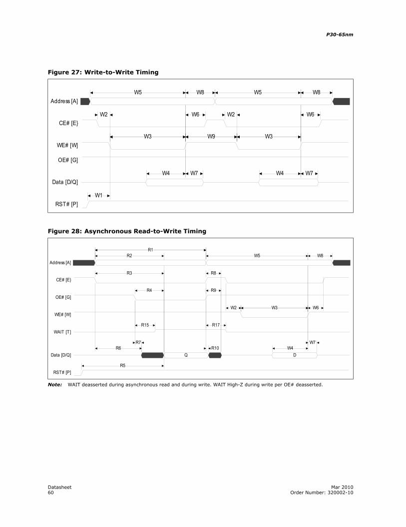
P30-65nm
Datasheet Mar 201060 Order Number: 320002-10
Note: WAIT deasserted during asynchronous read and during write. WAIT High-Z during write per OE# deasserted.
Figure 27: Write-to-Write Timing
W1
W7W4W7W4
W3W9 W3W9W3W3
W6W2W6W2
W8W8 W5W5Address [A]
CE# [E}
WE# [W]
OE# [G]
Data [D/Q]
RST# [P]
Figure 28: Asynchronous Read-to-Write Timing
Q D
R5
W7W4R10
R7R6
R17R15
W6W3W3W2
R9R4
R8R3
W8W5R1
R2R1
Address [A]
CE# [E}
OE# [G]
WE# [W]
WAIT [T]
Data [D/Q]
RST# [P]
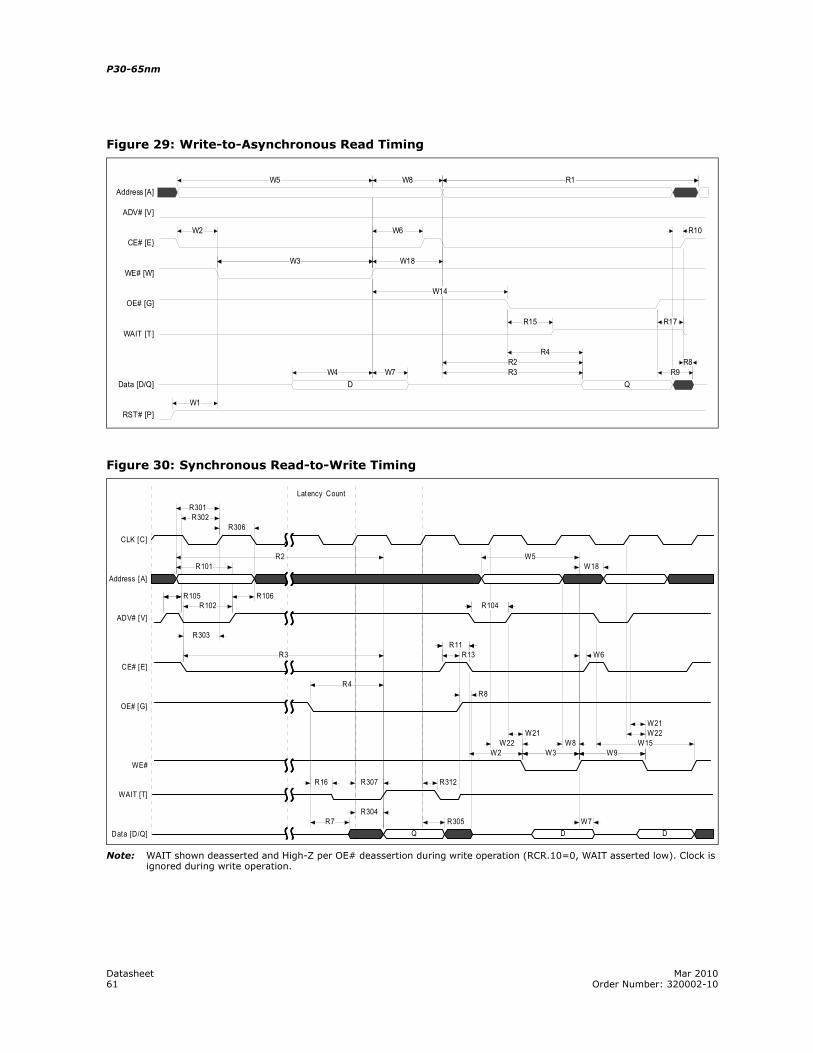
Datasheet Mar 201061 Order Number: 320002-10
P30-65nm
Note: WAIT shown deasserted and High-Z per OE# deassertion during write operation (RCR.10=0, WAIT asserted low). Clock is ignored during write operation.
Figure 29: Write-to-Asynchronous Read Timing
D Q
W1
R9R8
R4
R3R2
W7W4
R17R15
W14
W18W3W3
R10W6W2
R1R1W8W5Address [A]
ADV# [V]
CE# [E}
WE# [W]
OE# [G]
WAIT [T]
Data [D/Q]
RST# [P]
Figure 30: Synchronous Read-to-Write Timing
Latency Count
Q D DW7R305
R304R7
R312R307R16
W15W22W21
W9W8
W9W3W22
W21
W3W2
R8R4
W6R11
R13R11
R303
R3
R104R104R106
R102R105R105
W18W5
R101R2
R306R302
R301
CLK [C]
Address [A]
ADV# [V]
CE# [E]
OE# [G]
WE#
WAIT [T]
Data [D/Q]
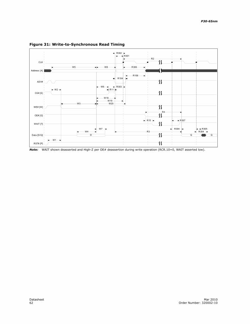
P30-65nm
Datasheet Mar 201062 Order Number: 320002-10
Note: WAIT shown deasserted and High-Z per OE# deassertion during write operation (RCR.10=0, WAIT asserted low).
Figure 31: Write-to-Synchronous Read Timing
D Q Q
W1
R304R305R304
R3W7
W4
R307R15
R4
W20W19
W18
W3W3
R11R303
R11W6
W2
R104R106
R104
R306W8W5
R302R301
R2CLK
Address [A]
ADV#
CE# [E}
WE# [W]
OE# [G]
WAIT [T]
Data [D/Q]
RST# [P]
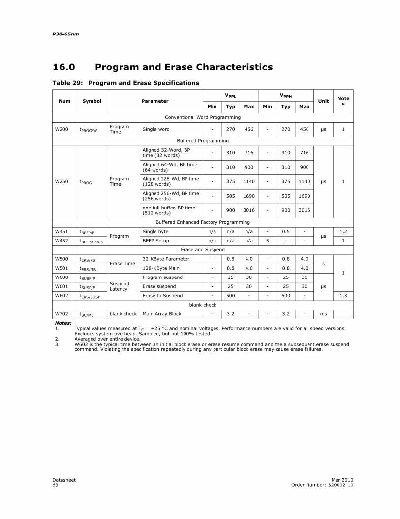
Datasheet Mar 201063 Order Number: 320002-10
P30-65nm
16.0 Program and Erase Characteristics
Table 29: Program and Erase Specifications
Num Symbol ParameterVPPL VPPH
Unit Notes
Min Typ Max Min Typ Max
Conventional Word Programming
W200 tPROG/WProgram Time Single word - 270 456 - 270 456 µs 1
Buffered Programming
W250 tPROGProgram Time
Aligned 32-Word, BP time (32 words) - 310 716 - 310 716
µs 1
Aligned 64-Wd, BP time (64 words) - 310 900 - 310 900
Aligned 128-Wd, BP time (128 words) - 375 1140 - 375 1140
Aligned 256-Wd, BP time (256 words) - 505 1690 - 505 1690
one full buffer, BP time (512 words) - 900 3016 - 900 3016
Buffered Enhanced Factory Programming
W451 tBEFP/BProgram
Single byte n/a n/a n/a - 0.5 -µs
1,2
W452 tBEFP/Setup BEFP Setup n/a n/a n/a 5 - - 1
Erase and Suspend
W500 tERS/PBErase Time
32-KByte Parameter - 0.8 4.0 - 0.8 4.0s
1W501 tERS/MB 128-KByte Main - 0.8 4.0 - 0.8 4.0
W600 tSUSP/PSuspend Latency
Program suspend - 25 30 - 25 30
µsW601 tSUSP/E Erase suspend - 25 30 - 25 30
W602 tERS/SUSP Erase to Suspend - 500 - - 500 - 1,3
blank check
W702 tBC/MB blank check Main Array Block - 3.2 - - 3.2 - ms
Notes:1. Typical values measured at TC = +25 °C and nominal voltages. Performance numbers are valid for all speed versions.
Excludes system overhead. Sampled, but not 100% tested.2. Averaged over entire device.3. W602 is the typical time between an initial block erase or erase resume command and the a subsequent erase suspend
command. Violating the specification repeatedly during any particular block erase may cause erase failures.
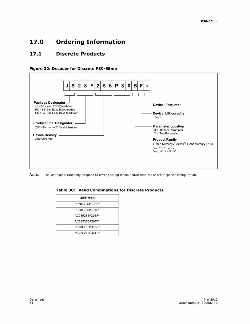
P30-65nm
Datasheet Mar 201064 Order Number: 320002-10
17.0 Ordering Information
17.1 Discrete Products
Note: The last digit is randomly assigned to cover packing media and/or features or other specific configuration.
Figure 32: Decoder for Discrete P30-65nm
F 2 5 P 3 0 B8S 2J 6
Product Line Designator28F = Numonyx™ Flash Memory
Package DesignatorJS = 56 -Lead TSOP, lead-freeRC = 64- Ball Easy BGA, leadedPC = 64 - Ball Easy BGA, lead-free
Device Density256 = 256-Mbit Product Family
P 30 = Numonyx® AxcellTM Flash Memory (P30)VCC = 1. 7 – 2. 0 VVCCQ = 1. 7 – 3. 6 V
Device Lithography
Parameter LocationB = Bottom ParameterT = Top Parameter
F
65 nm
*
Device Features*
Table 30: Valid Combinations for Discrete Products
256-Mbit
JS28F256P30BF*
JS28F256P30TF*
RC28F256P30BF*
RC28F256P30TF*
PC28F256P30BF*
PC28F256P30TF*
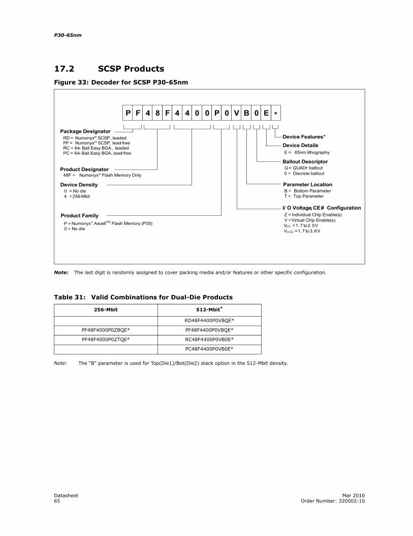
Datasheet Mar 201065 Order Number: 320002-10
P30-65nm
17.2 SCSP Products
Note: The last digit is randomly assigned to cover packing media and/or features or other specific configuration.
Note: The “B” parameter is used for Top(Die1)/Bot(Die2) stack option in the 512-Mbit density.
Figure 33: Decoder for SCSP P30-65nm
Table 31: Valid Combinations for Dual-Die Products
256-Mbit 512-Mbit*
RD48F4400P0VBQE*
PF48F4000P0ZBQE* PF48F4400P0VBQE*
PF48F4000P0ZTQE* RC48F4400P0VB0E*
PC48F4400P0VB0E*
Product Designator48F = Numonyx™ Flash Memory Only
Package DesignatorRD = Numonyx™ SCSP, leadedPF = Numonyx™ SCSP, lead- freeRC = 64- Ball Easy BGA , leadedPC = 64- Ball Easy BGA, lead-free
Device Density0 = No die4 = 256-Mbit
Product FamilyP = Numonyx® AxcellTM Flash Memory (P30)0 = No die
Device DetailsE = 65 nm lithography
Parameter LocationB = Bottom ParameterT = Top Parameter
F 4 4 P 0 B 08F 4P 0 E0 V
Ballout DescriptorQ = QUAD+ ballout0 = Discrete ballout
I/ O Voltage, CE# ConfigurationZ = Individual Chip Enable(s)V = Virtual Chip Enable(s)VCC = 1. 7 to 2. 0 VVCCQ = 1. 7 to 3.6 V
Device Features*
*
P30-65nm
Datasheet Mar 201066 Order Number: 320002-10
Appendix A Supplemental Reference Information
A.1 Common Flash Interface Tables
The Common Flash Interface (CFI) is part of an overall specification for multiple command-set and control-interface descriptions. This appendix describes the database structure containing the data returned by a read operation after issuing the Read CFI command (see Section 6.0, “Command Set” on page 21). System software can parse this database structure to obtain information about the flash device, such as block size, density, bus width, and electrical specifications. The system software will then know which command set(s) to use to properly perform flash writes, block erases, reads and otherwise control the flash device.
A.1.1 CFI Structure Output
The CFI database allows system software to obtain information for controlling the flash device. This section describes the device’s CFI-compliant interface that allows access to CFI data.
CFI data are presented on the lowest-order data outputs (DQ7-0) only. The numerical offset value is the address relative to the maximum bus width supported by the device. On this family of devices, the CFI table device starting address is a 10h, which is a word address for x16 devices.
For a word-wide (x16) device, the first two CFI-structure bytes, ASCII “Q” and “R,” appear on the low byte at word addresses 10h and 11h. This CFI-compliant device outputs 00h data on upper bytes. The device outputs ASCII “Q” in the low byte (DQ7-0) and 00h in the high byte (DQ15-8).
At CFI addresses containing two or more bytes of information, the least significant data byte is presented at the lower address, and the most significant data byte is presented at the higher address.
In all of the following tables, addresses and data are represented in hexadecimal notation, so the “h” suffix has been dropped. In addition, since the upper byte of word-wide devices is always “00h,” the leading “00” has been dropped from the table notation and only the lower byte value is shown. Any x16 device outputs can be assumed to have 00h on the upper byte in this mode.
Table 32: Summary of CFI Structure Output as a Function of Device and Mode
Device HexOffset
HexCode
ASCIIValue
00010: 51 "Q"Device Addresses 00011: 52 "R"
00012: 59 "Y"
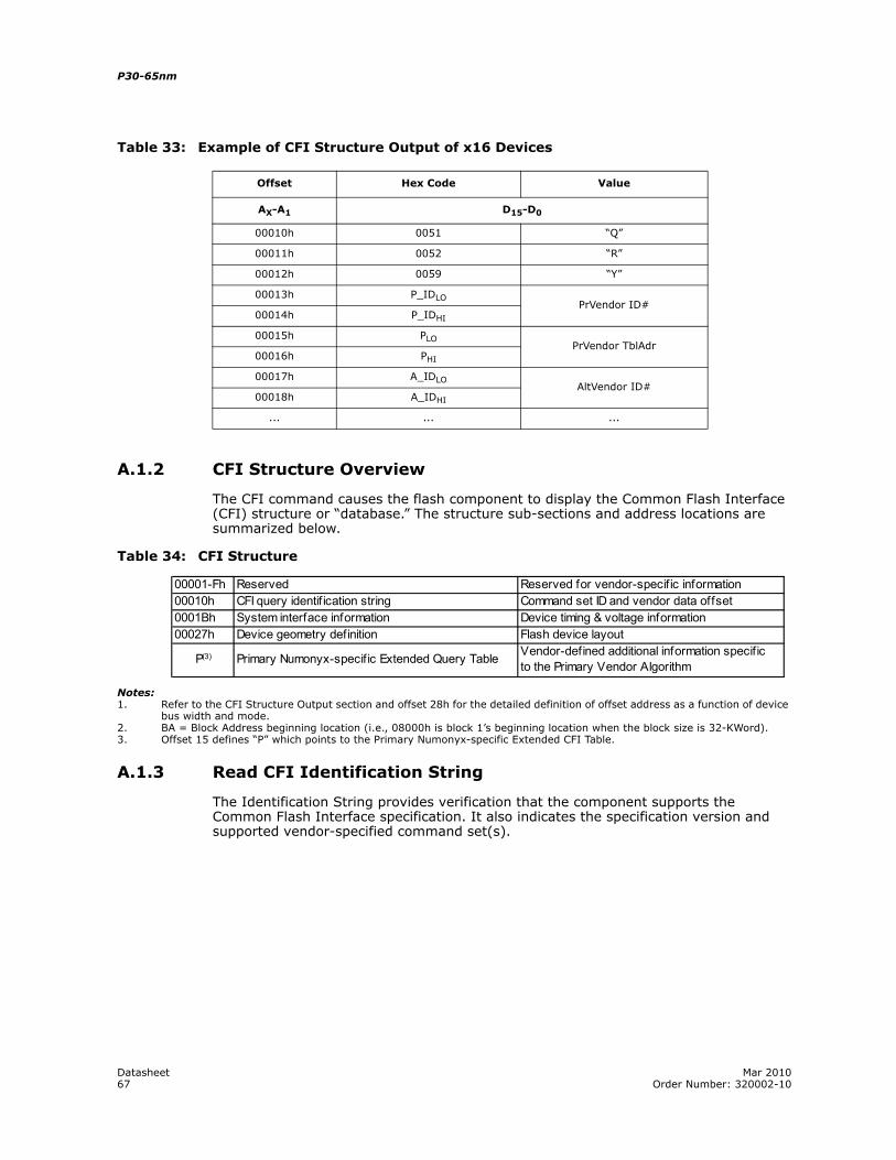
Datasheet Mar 201067 Order Number: 320002-10
P30-65nm
Table 33: Example of CFI Structure Output of x16 Devices
A.1.2 CFI Structure Overview
The CFI command causes the flash component to display the Common Flash Interface (CFI) structure or “database.” The structure sub-sections and address locations are summarized below.
Table 34: CFI Structure
Notes:1. Refer to the CFI Structure Output section and offset 28h for the detailed definition of offset address as a function of device
bus width and mode.2. BA = Block Address beginning location (i.e., 08000h is block 1’s beginning location when the block size is 32-KWord).3. Offset 15 defines “P” which points to the Primary Numonyx-specific Extended CFI Table.
A.1.3 Read CFI Identification String
The Identification String provides verification that the component supports the Common Flash Interface specification. It also indicates the specification version and supported vendor-specified command set(s).
Offset Hex Code Value
AX-A1 D15-D0
00010h 0051 “Q”
00011h 0052 “R”
00012h 0059 “Y”
00013h P_IDLOPrVendor ID#
00014h P_IDHI
00015h PLOPrVendor TblAdr
00016h PHI
00017h A_IDLOAltVendor ID#
00018h A_IDHI
... ... ...
00001-Fh Reserved Reserved for vendor-specific information00010h CFI query identif ication string Command set ID and vendor data offset0001Bh System interface information Device timing & voltage information00027h Device geometry definition Flash device layout
P(3) Primary Numonyx-specific Extended Query Table Vendor-defined additional information specificto the Primary Vendor Algorithm
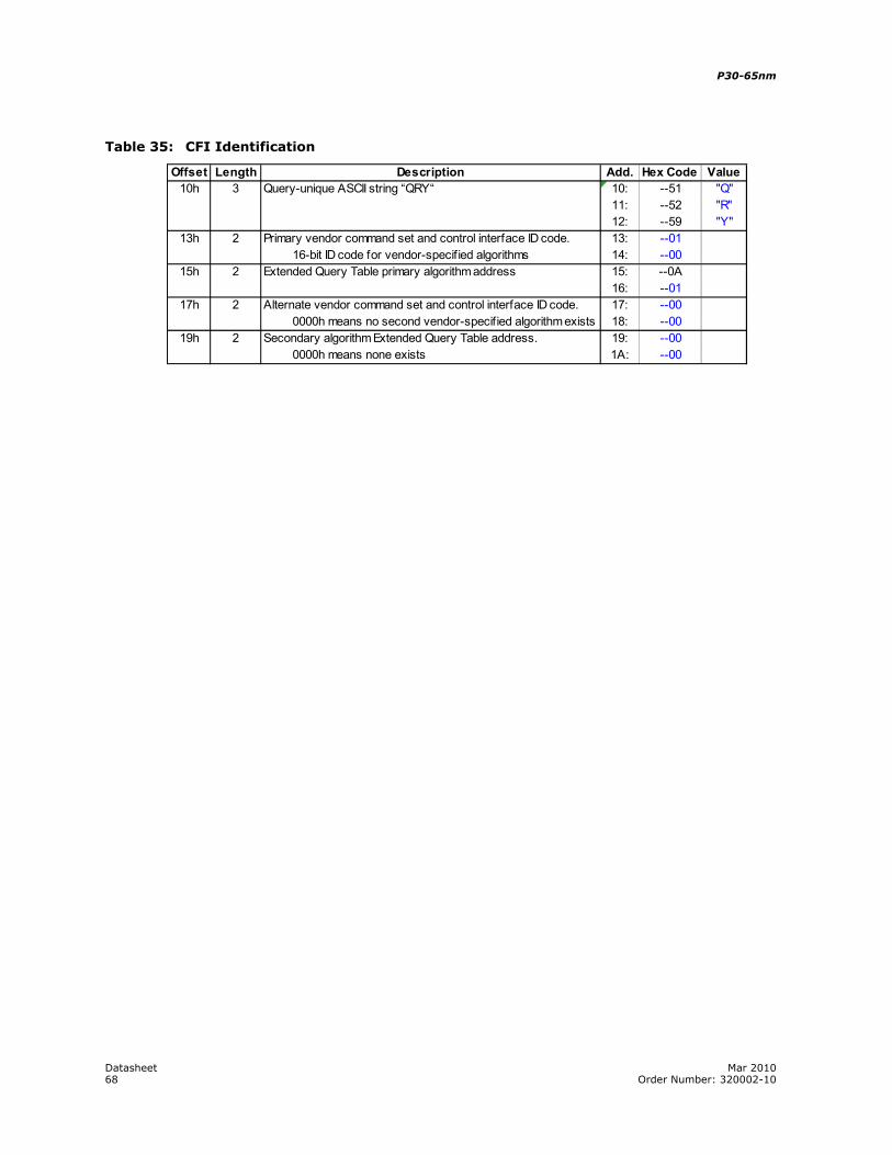
P30-65nm
Datasheet Mar 201068 Order Number: 320002-10
Table 35: CFI Identification
Offset Length Description Add. Hex Code Value10h 3 Query-unique ASCII string “QRY“ 10: --51 "Q"
11: --52 "R"12: --59 "Y"
13h 2 Primary vendor command set and control interface ID code. 13: --0116-bit ID code for vendor-specified algorithms 14: --00
15h 2 Extended Query Table primary algorithm address 15: --0A16: --01
17h 2 Alternate vendor command set and control interface ID code. 17: --000000h means no second vendor-specified algorithm exists 18: --00
19h 2 Secondary algorithm Extended Query Table address. 19: --000000h means none exists 1A: --00
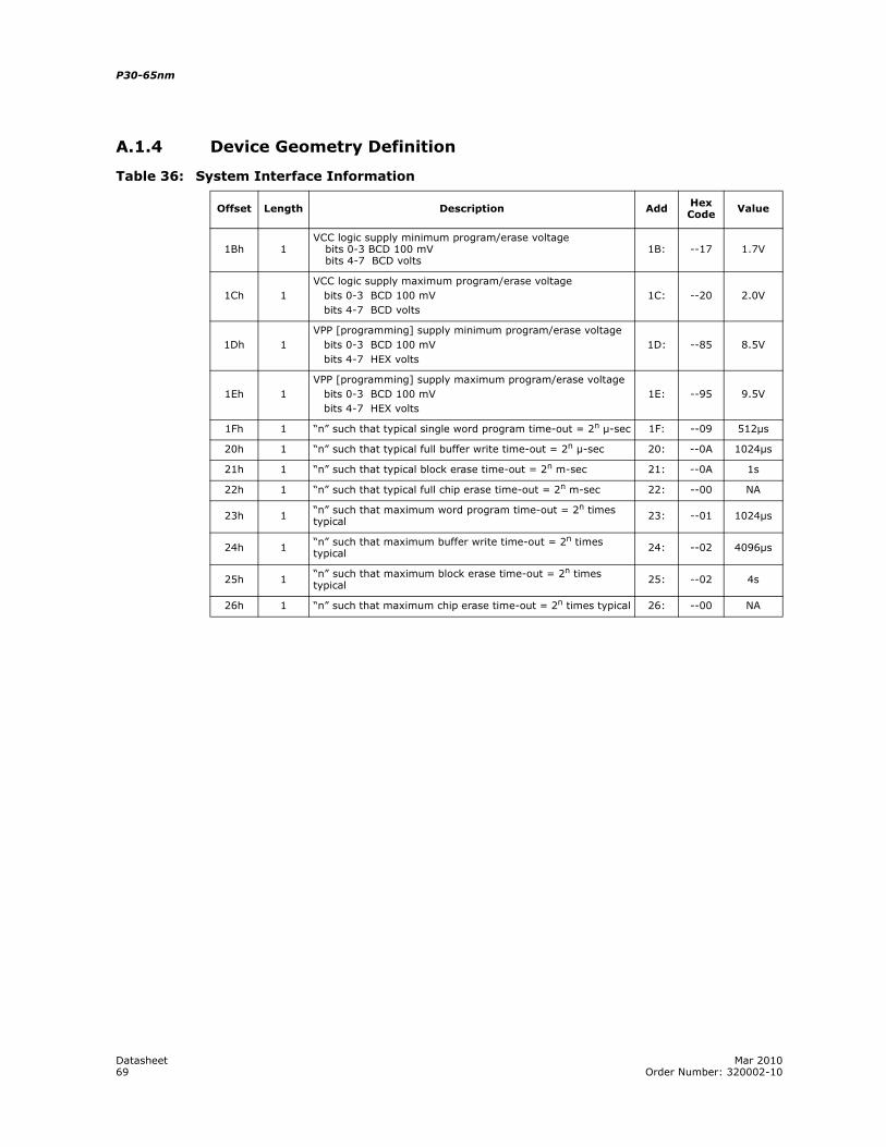
Datasheet Mar 201069 Order Number: 320002-10
P30-65nm
A.1.4 Device Geometry Definition
Table 36: System Interface Information
Offset Length Description Add HexCode Value
1Bh 1VCC logic supply minimum program/erase voltage
bits 0-3 BCD 100 mVbits 4-7 BCD volts
1B: --17 1.7V
1Ch 1VCC logic supply maximum program/erase voltage bits 0-3 BCD 100 mV bits 4-7 BCD volts
1C: --20 2.0V
1Dh 1VPP [programming] supply minimum program/erase voltage bits 0-3 BCD 100 mV bits 4-7 HEX volts
1D: --85 8.5V
1Eh 1VPP [programming] supply maximum program/erase voltage bits 0-3 BCD 100 mV bits 4-7 HEX volts
1E: --95 9.5V
1Fh 1 “n” such that typical single word program time-out = 2n µ-sec 1F: --09 512µs
20h 1 “n” such that typical full buffer write time-out = 2n µ-sec 20: --0A 1024µs
21h 1 “n” such that typical block erase time-out = 2n m-sec 21: --0A 1s
22h 1 “n” such that typical full chip erase time-out = 2n m-sec 22: --00 NA
23h 1 “n” such that maximum word program time-out = 2n times typical 23: --01 1024µs
24h 1 “n” such that maximum buffer write time-out = 2n times typical 24: --02 4096µs
25h 1 “n” such that maximum block erase time-out = 2n times typical 25: --02 4s
26h 1 “n” such that maximum chip erase time-out = 2n times typical 26: --00 NA
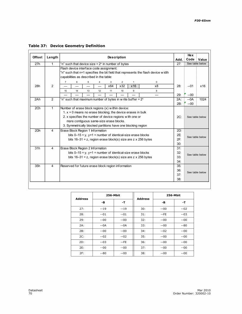
P30-65nm
Datasheet Mar 201070 Order Number: 320002-10
Table 37: Device Geometry Definition
Offset Length DescriptionAdd.
HexCode Value
27h 1 “n” such that device size = 2n in number of bytes 27:
7 6 5 4 3 2 1 0
28h 2 — — — — x64 x32 x16 x8 28: --01 x1615 14 13 12 11 10 9 8
— — — — — — — — 29: --002Ah 2 “n” such that maximum number of bytes in w rite buffer = 2n 2A: --0A 1024
2B: --002Ch 1
2C:
2Dh 4 Erase Block Region 1 Information 2D:bits 0–15 = y, y+1 = number of identical-size erase blocks 2E:bits 16–31 = z, region erase block(s) size are z x 256 bytes 2F:
30:31h 4 Erase Block Region 2 Information 31:
bits 0–15 = y, y+1 = number of identical-size erase blocks 32:bits 16–31 = z, region erase block(s) size are z x 256 bytes 33:
34:35h 4 Reserved for future erase block region information 35:
36:37:38:
See table below
See table below
See table below
See table below
See table below
Number of erase block regions (x) w ithin device: 1. x = 0 means no erase blocking; the device erases in bulk 2. x specif ies the number of device regions w ith one or more contiguous same-size erase blocks. 3. Symmetrically blocked partitions have one blocking region
Flash device interface code assignment:"n" such that n+1 specif ies the bit f ield that represents the flash device w idthcapabilities as described in the table:
Address256-Mbit
Address256-Mbit
-B -T -B -T
27: --19 --19 30: --00 --02
28: --01 --01 31: --FE --03
29: --00 --00 32: --00 --00
2A: --0A --0A 33: --00 --80
2B: --00 --00 34: --02 --00
2C: --02 --02 35: --00 --00
2D: --03 --FE 36: --00 --00
2E: --00 --00 37: --00 --00
2F: --80 --00 38: --00 --00
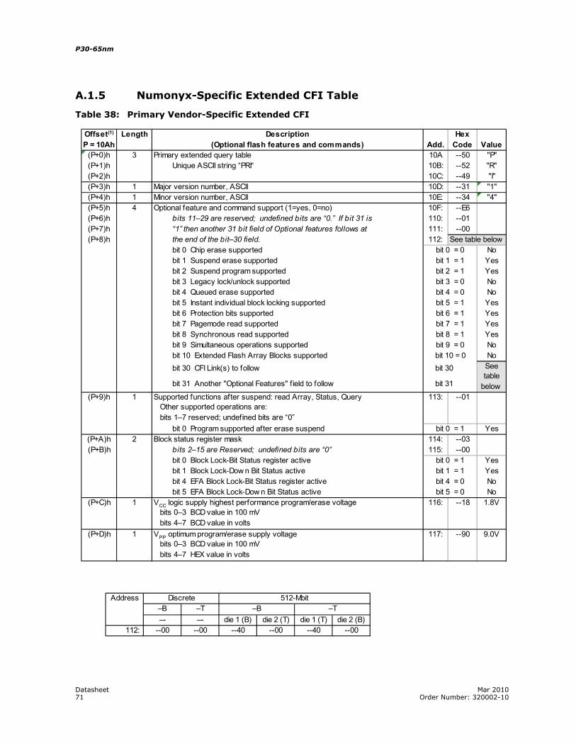
Datasheet Mar 201071 Order Number: 320002-10
P30-65nm
A.1.5 Numonyx-Specific Extended CFI Table
Table 38: Primary Vendor-Specific Extended CFI
Offset(1) Length Description HexP = 10Ah (Optional flash features and commands) Add. Code Value
(P+0)h 3 Primary extended query table 10A --50 "P"(P+1)h Unique ASCII string “PRI“ 10B: --52 "R"(P+2)h 10C: --49 "I"(P+3)h 1 Major version number, ASCII 10D: --31 "1"(P+4)h 1 Minor version number, ASCII 10E: --34 "4"(P+5)h 4 Optional feature and command support (1=yes, 0=no) 10F: --E6(P+6)h bits 11–29 are reserved; undefined bits are “0.” If bit 31 is 110: --01(P+7)h “1” then another 31 bit field of Optional features follows at 111: --00(P+8)h the end of the bit–30 field. 112:
bit 0 Chip erase supported bit 0 = 0 Nobit 1 Suspend erase supported bit 1 = 1 Yesbit 2 Suspend program supported bit 2 = 1 Yesbit 3 Legacy lock/unlock supported bit 3 = 0 Nobit 4 Queued erase supported bit 4 = 0 Nobit 5 Instant individual block locking supported bit 5 = 1 Yesbit 6 Protection bits supported bit 6 = 1 Yesbit 7 Pagemode read supported bit 7 = 1 Yesbit 8 Synchronous read supported bit 8 = 1 Yesbit 9 Simultaneous operations supported bit 9 = 0 Nobit 10 Extended Flash Array Blocks supported bit 10 = 0 Nobit 30 CFI Link(s) to follow bit 30
bit 31 Another "Optional Features" field to follow bit 31
(P+9)h 1 113: --01
bit 0 Program supported after erase suspend bit 0 = 1 Yes(P+A)h 2 Block status register mask 114: --03(P+B)h bits 2–15 are Reserved; undefined bits are “0” 115: --00
bit 0 Block Lock-Bit Status register active bit 0 = 1 Yesbit 1 Block Lock-Dow n Bit Status active bit 1 = 1 Yesbit 4 EFA Block Lock-Bit Status register active bit 4 = 0 Nobit 5 EFA Block Lock-Dow n Bit Status active bit 5 = 0 No
(P+C)h 1 116: --18 1.8V
(P+D)h 1 117: --90 9.0V
See table below
Seetable
belowSupported functions after suspend: read Array, Status, Query Other supported operations are: bits 1–7 reserved; undefined bits are “0”
VPP optimum program/erase supply voltage bits 0–3 BCD value in 100 mV bits 4–7 HEX value in volts
VCC logic supply highest performance program/erase voltage bits 0–3 BCD value in 100 mV bits 4–7 BCD value in volts
Discrete–B –T–- –- die 1 (B) die 2 (T) die 1 (T) die 2 (B)
112: --00 --00 --40 --00 --40 --00
512-MbitAddress–B –T
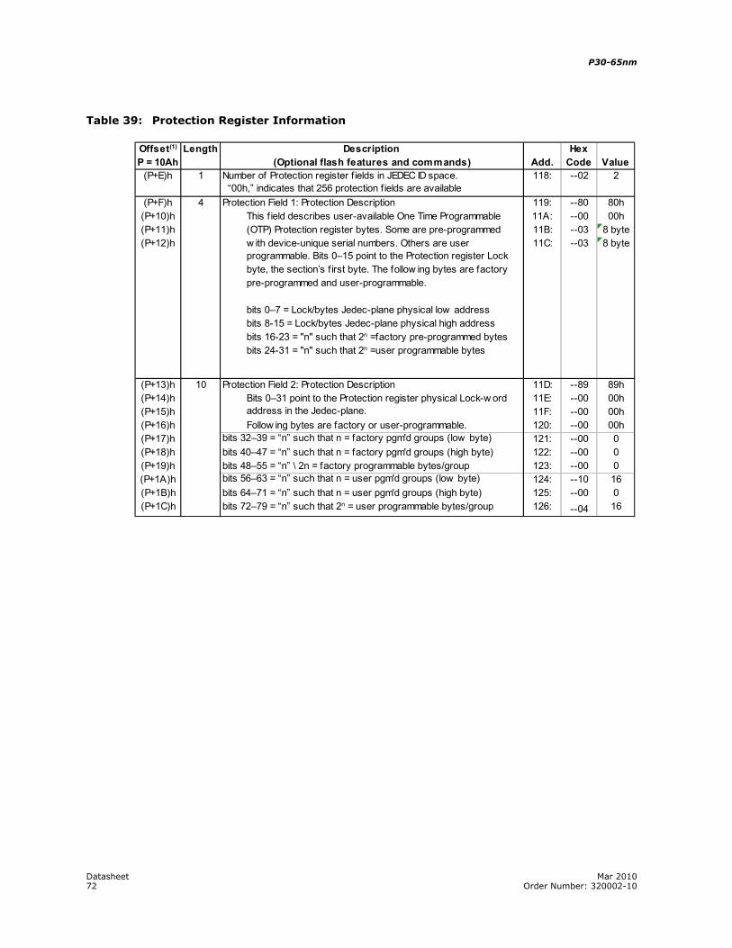
P30-65nm
Datasheet Mar 201072 Order Number: 320002-10
Table 39: Protection Register Information
Offset(1) Length Description HexP = 10Ah (Optional flash features and commands) Add. Code Value
(P+E)h 1 118: --02 2
(P+F)h 4 Protection Field 1: Protection Description 119: --80 80h(P+10)h This f ield describes user-available One Time Programmable 11A: --00 00h(P+11)h (OTP) Protection register bytes. Some are pre-programmed 11B: --03 8 byte(P+12)h 11C: --03 8 byte
(P+13)h 10 Protection Field 2: Protection Description 11D: --89 89h(P+14)h 11E: --00 00h(P+15)h 11F: --00 00h(P+16)h 120: --00 00h(P+17)h 121: --00 0(P+18)h bits 40–47 = “n” such that n = factory pgm'd groups (high byte) 122: --00 0(P+19)h 123: --00 0(P+1A)h 124: --10 16(P+1B)h 125: --00 0(P+1C)h 126: --04 16
Number of Protection register f ields in JEDEC ID space. “00h,” indicates that 256 protection f ields are available
w ith device-unique serial numbers. Others are userprogrammable. Bits 0–15 point to the Protection register Lockbyte, the section’s f irst byte. The follow ing bytes are factorypre-programmed and user-programmable.
bits 0–7 = Lock/bytes Jedec-plane physical low addressbits 8-15 = Lock/bytes Jedec-plane physical high addressbits 16-23 = "n" such that 2n =factory pre-programmed bytesbits 24-31 = "n" such that 2n =user programmable bytes
Bits 0–31 point to the Protection register physical Lock-w ordaddress in the Jedec-plane.Follow ing bytes are factory or user-programmable.
bits 32–39 = “n” such that n = factory pgm'd groups (low byte)
bits 48–55 = “n” \ 2n = factory programmable bytes/groupbits 56–63 = “n” such that n = user pgm'd groups (low byte)bits 64–71 = “n” such that n = user pgm'd groups (high byte)bits 72–79 = “n” such that 2n = user programmable bytes/group
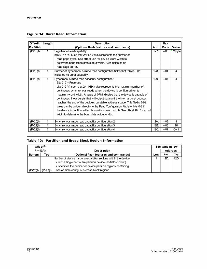
Datasheet Mar 201073 Order Number: 320002-10
P30-65nm
Table 40: Partition and Erase Block Region Information
Figure 34: Burst Read Information
Offset(1) Length Description HexP = 10Ah (Optional flash features and commands) Add. Code Value(P+1D)h 1 127: --05 32 byte
(P+1E)h 1 128: --04 4
(P+1F)h 1 129: --01 4
(P+20)h 1 Synchronous mode read capability configuration 2 12A: --02 8(P+21)h 1 Synchronous mode read capability configuration 3 12B: --03 16(P+22)h 1 Synchronous mode read capability configuration 4 12C: --07 Cont
Page Mode Read capabilitybits 0–7 = “n” such that 2n HEX value represents the number of read-page bytes. See offset 28h for device word w idth to determine page-mode data output w idth. 00h indicates no read page buffer.
Synchronous mode read capability configuration 1 Bits 3–7 = Reserved bits 0–2 “n” such that 2n+1 HEX value represents the maximum number of continuous synchronous reads w hen the device is configured for its maximum w ord w idth. A value of 07h indicates that the device is capable of continuous linear bursts that w ill output data until the internal burst counter reaches the end of the device's burstable address space. This filed's 3-bit value can be written directly to the Read Configuration Register bits 0-2 if the device is configured for its maximum word w idth. See offset 28h for w ord w idth to determine the burst data output w idth.
Number of synchronous mode read configuration fields that follow . 00hindicates no burst capability.
Offset(1) See table belowP = 10Ah Description Address
Bottom Top (Optional flash features and commands) Len Bot Top
(P+23)h (P+23)h
1 12D: 12D:Number of device hardw are-partition regions w ithin the device. x = 0: a single hardw are partition device (no fields follow ). x specifies the number of device partition regions containing one or more contiguous erase block regions.
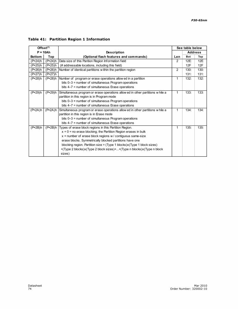
P30-65nm
Datasheet Mar 201074 Order Number: 320002-10
Table 41: Partition Region 1 Information
Offset(1) See table belowP = 10Ah Description Address
Bottom Top (Optional flash features and commands) Len Bot Top(P+24)h (P+24)h Data size of this Parition Region Information f ield 2 12E: 12E(P+25)h (P+25)h (# addressable locations, including this f ield) 12F 12F(P+26)h (P+26)h Number of identical partitions w ithin the partition region 2 130: 130:(P+27)h (P+27)h 131: 131:(P+28)h (P+28)h 1 132: 132:
(P+29)h (P+29)h 1 133: 133:
(P+2A)h (P+2A)h 1 134: 134:
(P+2B)h (P+2B)h 1 135: 135:Types of erase block regions in this Partition Region. x = 0 = no erase blocking; the Partition Region erases in bulk x = number of erase block regions w / contiguous same-size erase blocks. Symmetrically blocked partitions have one blocking region. Partition size = (Type 1 blocks)x(Type 1 block sizes) +(Type 2 blocks)x(Type 2 block sizes)+...+(Type n blocks)x(Type n block sizes)
Number of program or erase operations allow ed in a partition bits 0–3 = number of simultaneous Program operations bits 4–7 = number of simultaneous Erase operations
Simultaneous program or erase operations allow ed in other partitions w hile apartition in this region is in Program mode bits 0–3 = number of simultaneous Program operations bits 4–7 = number of simultaneous Erase operationsSimultaneous program or erase operations allow ed in other partitions w hile apartition in this region is in Erase mode bits 0–3 = number of simultaneous Program operations bits 4–7 = number of simultaneous Erase operations
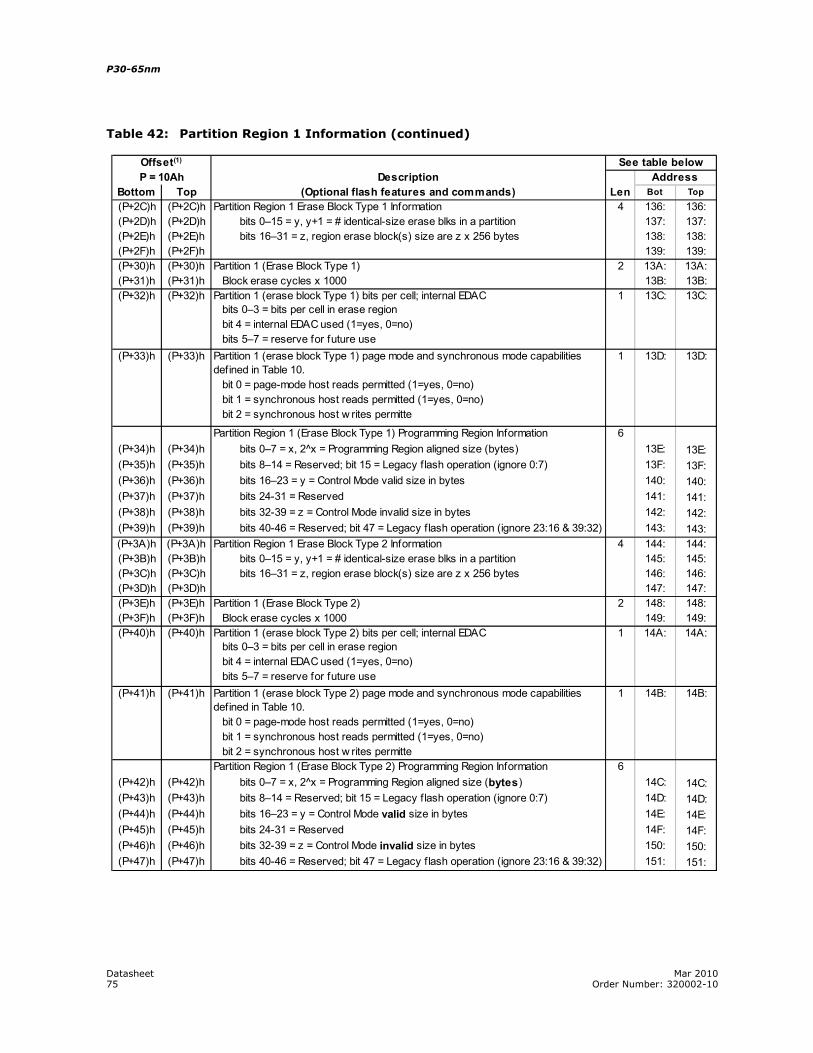
Datasheet Mar 201075 Order Number: 320002-10
P30-65nm
Table 42: Partition Region 1 Information (continued)
Offset(1) See table belowP = 10Ah Description Address
Bottom Top (Optional flash features and commands) Len Bot Top(P+2C)h (P+2C)h Partition Region 1 Erase Block Type 1 Information 4 136: 136:(P+2D)h (P+2D)h bits 0–15 = y, y+1 = # identical-size erase blks in a partition 137: 137:(P+2E)h (P+2E)h bits 16–31 = z, region erase block(s) size are z x 256 bytes 138: 138:(P+2F)h (P+2F)h 139: 139:(P+30)h (P+30)h Partition 1 (Erase Block Type 1) 2 13A: 13A:(P+31)h (P+31)h Block erase cycles x 1000 13B: 13B:(P+32)h (P+32)h 1 13C: 13C:
(P+33)h (P+33)h 1 13D: 13D:
Partition Region 1 (Erase Block Type 1) Programming Region Information 6(P+34)h (P+34)h bits 0–7 = x, 2^x = Programming Region aligned size (bytes) 13E: 13E:(P+35)h (P+35)h bits 8–14 = Reserved; bit 15 = Legacy flash operation (ignore 0:7) 13F: 13F:(P+36)h (P+36)h bits 16–23 = y = Control Mode valid size in bytes 140: 140:(P+37)h (P+37)h bits 24-31 = Reserved 141: 141:(P+38)h (P+38)h bits 32-39 = z = Control Mode invalid size in bytes 142: 142:(P+39)h (P+39)h bits 40-46 = Reserved; bit 47 = Legacy flash operation (ignore 23:16 & 39:32) 143: 143:(P+3A)h (P+3A)h Partition Region 1 Erase Block Type 2 Information 4 144: 144:(P+3B)h (P+3B)h bits 0–15 = y, y+1 = # identical-size erase blks in a partition 145: 145:(P+3C)h (P+3C)h bits 16–31 = z, region erase block(s) size are z x 256 bytes 146: 146:(P+3D)h (P+3D)h 147: 147:(P+3E)h (P+3E)h Partition 1 (Erase Block Type 2) 2 148: 148:(P+3F)h (P+3F)h Block erase cycles x 1000 149: 149:(P+40)h (P+40)h 1 14A: 14A:
(P+41)h (P+41)h 1 14B: 14B:
Partition Region 1 (Erase Block Type 2) Programming Region Information 6(P+42)h (P+42)h bits 0–7 = x, 2^x = Programming Region aligned size (bytes) 14C: 14C:(P+43)h (P+43)h bits 8–14 = Reserved; bit 15 = Legacy flash operation (ignore 0:7) 14D: 14D:(P+44)h (P+44)h bits 16–23 = y = Control Mode valid size in bytes 14E: 14E:(P+45)h (P+45)h bits 24-31 = Reserved 14F: 14F:(P+46)h (P+46)h bits 32-39 = z = Control Mode invalid size in bytes 150: 150:(P+47)h (P+47)h bits 40-46 = Reserved; bit 47 = Legacy flash operation (ignore 23:16 & 39:32) 151: 151:
Partition 1 (erase block Type 1) page mode and synchronous mode capabilitiesdefined in Table 10. bit 0 = page-mode host reads permitted (1=yes, 0=no) bit 1 = synchronous host reads permitted (1=yes, 0=no) bit 2 = synchronous host w rites permitte
Partition 1 (erase block Type 1) bits per cell; internal EDAC bits 0–3 = bits per cell in erase region bit 4 = internal EDAC used (1=yes, 0=no) bits 5–7 = reserve for future use
Partition 1 (erase block Type 2) bits per cell; internal EDAC bits 0–3 = bits per cell in erase region bit 4 = internal EDAC used (1=yes, 0=no) bits 5–7 = reserve for future usePartition 1 (erase block Type 2) page mode and synchronous mode capabilitiesdefined in Table 10. bit 0 = page-mode host reads permitted (1=yes, 0=no) bit 1 = synchronous host reads permitted (1=yes, 0=no) bit 2 = synchronous host w rites permitte
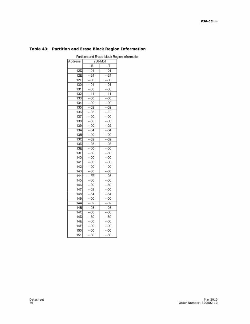
P30-65nm
Datasheet Mar 201076 Order Number: 320002-10
Table 43: Partition and Erase Block Region Information
Partition and Erase-block Region InformationAddress
–B –T12D: --01 --0112E: --24 --2412F: --00 --00130: --01 --01131: --00 --00132: --11 --11133: --00 --00134: --00 --00135: --02 --02136: --03 --FE137: --00 --00138: --80 --00139: --00 --0213A --64 --6413B: --00 --0013C: --02 --0213D: --03 --0313E: --00 --0013F: --80 --80140: --00 --00141: --00 --00142: --00 --00143: --80 --80144: --FE --03145: --00 --00146: --00 --80147: --02 --00148: --64 --64149: --00 --0014A --02 --0214B: --03 --0314C: --00 --0014D: --80 --8014E: --00 --0014F: --00 --00150: --00 --00151: --80 --80
256-Mbit
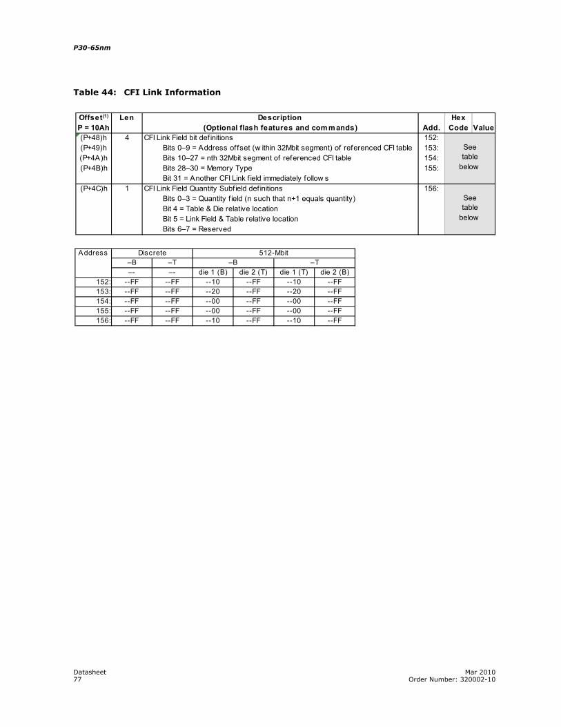
Datasheet Mar 201077 Order Number: 320002-10
P30-65nm
Table 44: CFI Link Information
Offset(1) Len Description HexP = 10Ah (Optional flash features and com m ands) Add. Code Value(P+48)h 4 CFI Link Field bit def initions 152:(P+49)h Bits 0–9 = Address offset (w ithin 32Mbit segment) of referenced CFI table 153:(P+4A)h Bits 10–27 = nth 32Mbit segment of referenced CFI table 154:(P+4B)h Bits 28–30 = Memory Type 155:
Bit 31 = Another CFI Link f ield immediately follow s(P+4C)h 1 CFI Link Field Quantity Subf ield def initions 156:
Bits 0–3 = Quantity f ield (n such that n+1 equals quantity)Bit 4 = Table & Die relative locationBit 5 = Link Field & Table relative locationBits 6–7 = Reserved
Seetable
below
Seetable
below
Discrete–B –T–- –- die 1 (B) die 2 (T) die 1 (T) die 2 (B)
152: --FF --FF --10 --FF --10 --FF153: --FF --FF --20 --FF --20 --FF154: --FF --FF --00 --FF --00 --FF155: --FF --FF --00 --FF --00 --FF156: --FF --FF --10 --FF --10 --FF
Address 512-Mbit–B –T
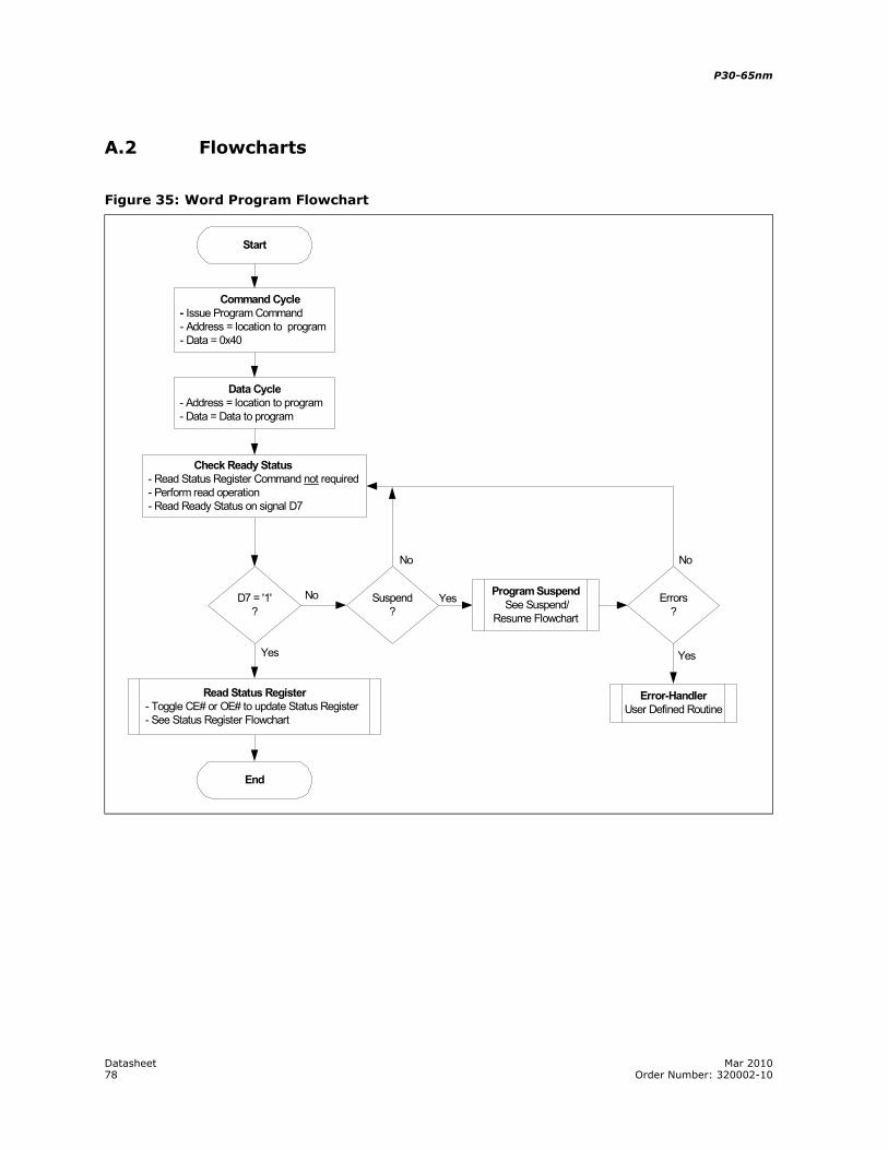
P30-65nm
Datasheet Mar 201078 Order Number: 320002-10
A.2 Flowcharts
Figure 35: Word Program Flowchart
Start
Data Cycle- Address = location to program - Data = Data to program
Yes
D7 = '1'?
End
No Suspend?
No
Yes Errors?
Yes
No
Error-HandlerUser Defined Routine
Read Status Register- Toggle CE# or OE# to update Status Register- See Status Register Flowchart
Program Suspend See Suspend/
Resume Flowchart
Command Cycle- Issue Program Command- Address = location to program- Data = 0x40
Check Ready Status - Read Status Register Command not required- Perform read operation - Read Ready Status on signal D7
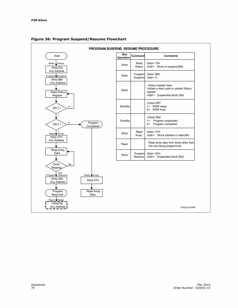
Datasheet Mar 201079 Order Number: 320002-10
P30-65nm
Figure 36: Program Suspend/Resume Flowchart
Read Status Register
SR.7 =
SR.2 =
Read Array Data
Program Completed
DoneReading
Program Resumed
Read Array Data
0
No
0
Yes
1
1
PROGRAM SUSPEND / RESUME PROCEDURE
Write Program Resume
Data = D0hAddr = Suspended block (BA)
Bus Operation Command Comments
Write Program Suspend
Data = B0hAddr = X
StandbyCheck SR.71 = WSM ready0 = WSM busy
StandbyCheck SR.21 = Program suspended0 = Program completed
Write Read Array
Data = FFhAddr = Block address to read (BA)
Read Read array data from block other than the one being programmed
Read
Status register dataInitiate a read cycle to update Status registerAddr = Suspended block (BA)
PGM_ SUS. WMF
Start
Write B0hAny Address
Program Suspend
Read Status
Write 70h
Write FFhAny Address
Read Array
Write D0hAny Address
Program Resume
Write FFh
Read Array
Write Read Status
Data = 70hAddr = Block to suspend (BA)
Write 70hAny Address
Read Status
Any Address
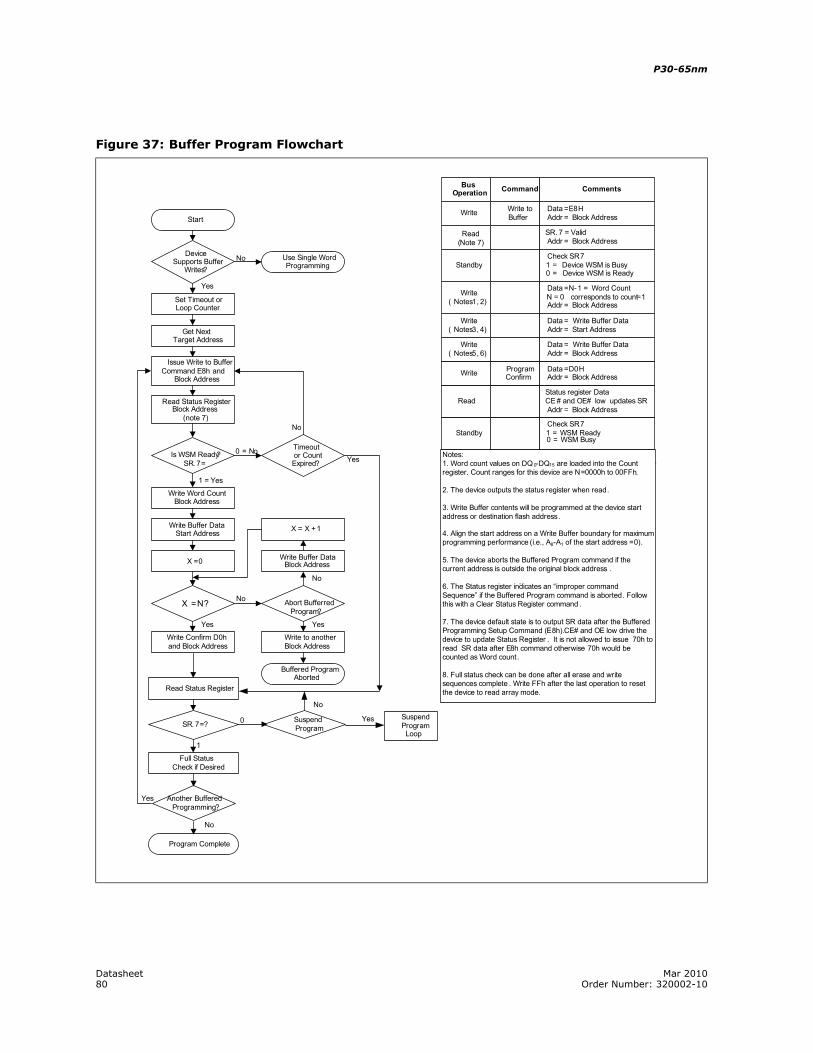
P30-65nm
Datasheet Mar 201080 Order Number: 320002-10
Figure 37: Buffer Program Flowchart
Start
Get NextTarget Address
Issue Write to Buffer Command E8h and
Block Address
Read Status Register Block Address
(note 7)
Is WSM Ready?SR. 7 =
1 = Yes
DeviceSupports Buffer
Writes?
Set Timeout or Loop Counter
Timeoutor Count Expired?
Write Confirm D0hand Block Address
Another Buffered Programming?
Yes
No
No
Write Buffer DataStart Address
X = 0
Yes
0 = No
No
Yes
Use Single Word Programming
Abort Bufferred Program?
No
X = N?
Write Buffer DataBlock Address
X = X + 1
Write to another Block Address
Buffered Program Aborted
No
YesYes
Write Word CountBlock Address
Notes:1. Word count values on DQ 0-DQ15 are loaded into the Count register. Count ranges for this device are N=0000h to 00FFh.
2. The device outputs the status register when read.
3. Write Buffer contents will be programmed at the device start address or destination flash address .
4. Align the start address on a Write Buffer boundary for maximum programming performance (i.e., A8-A1 of the start address =0).
5. The device aborts the Buffered Program command if the current address is outside the original block address .
6. The Status register indicates an “improper command Sequence” if the Buffered Program command is aborted. Follow this with a Clear Status Register command .
7. The device default state is to output SR data after the Buffered Programming Setup Command (E8h).CE# and OE low drive the device to update Status Register . It is not allowed to issue 70h to read SR data after E8h command otherwise 70h would be counted as Word count.
8. Full status check can be done after all erase and write sequences complete . Write FFh after the last operation to reset the device to read array mode.
.
.
.
BusOperation
Standby
Read
Command
Write Write to Buffer
Read(Note 7)
Standby
Comments
Check SR.71 = WSM Ready0 = WSM Busy
Status register Data CE # and OE# low updates SRAddr = Block Address
Data = E8HAddr = Block Address
SR. 7 = ValidAddr = Block Address
Check SR.71 = Device WSM is Busy0 = Device WSM is Ready
Write Program Confirm
Data = D0HAddr = Block Address
Write( Notes 1, 2)
Data = N-1 = Word CountN = 0 corresponds to count = 1Addr = Block Address
Write( Notes 3, 4)
Data = Write Buffer DataAddr = Start Address
Write( Notes 5, 6)
Data = Write Buffer DataAddr = Block Address
Suspend Program Loop
Read Status Register
SR. 7 =?
Full StatusCheck if Desired
Program Complete
Suspend Program
1
0
No
Yes
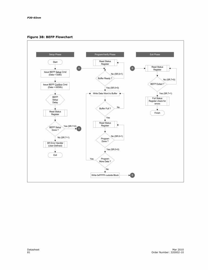
Datasheet Mar 201081 Order Number: 320002-10
P30-65nm
Figure 38: BEFP Flowchart
SR Error Handler(User-Defined)
BEFP Setup Delay
Yes (SR.7=0)A
Issue BEFP Setup Cmd(Data = 0x80)
Issue BEFP Confirm Cmd(Data = 00D0h)
Read Status Register
No (SR.7=1)
Exit
Start
Yes (SR.0=0)
No (SR.0=1)
Write 0xFFFFh outside Block
No (SR.0=1)
Yes (SR.0=0)
No
Yes
Yes (SR.7=1)
No (SR.7=0)
Finish
No
Yes
BEFP Setup Done ?
Full Status Register check for
errors
Read Status Register
Buffer Ready ?
Write Data Word to Buffer
Buffer Full ?
Read Status Register
ProgramDone ?
ProgramMore Data ?
Program/Verify PhaseSetup Phase Exit Phase
A B
B
BEFP Exited ?
Read Status Register
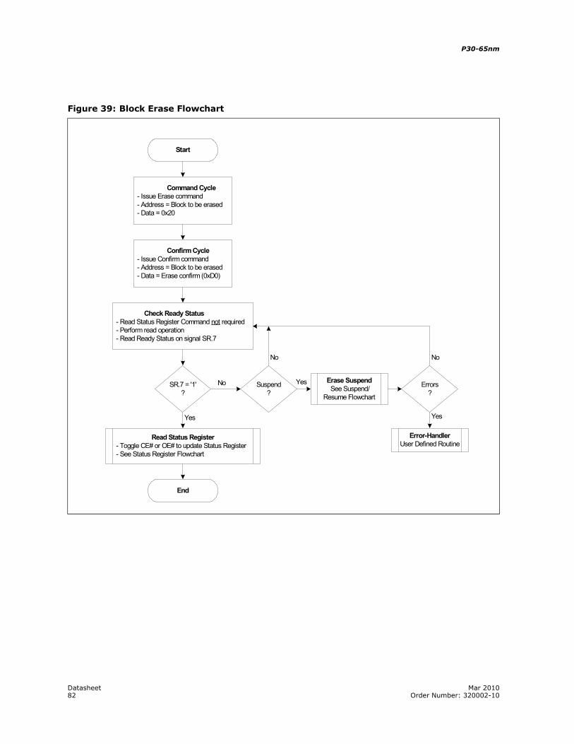
P30-65nm
Datasheet Mar 201082 Order Number: 320002-10
Figure 39: Block Erase Flowchart
Start
Confirm Cycle - Issue Confirm command - Address = Block to be erased - Data = Erase confirm (0xD0)
Errors?
Yes
No
Error-HandlerUser Defined Routine
Check Ready Status - Read Status Register Command not required - Perform read operation - Read Ready Status on signal SR.7
Command Cycle - Issue Erase command - Address = Block to be erased - Data = 0x20
Yes
SR.7 = '1'?
End
No Suspend?
No
Yes
Read Status Register - Toggle CE# or OE# to update Status Register - See Status Register Flowchart
Erase Suspend See Suspend/
Resume Flowchart
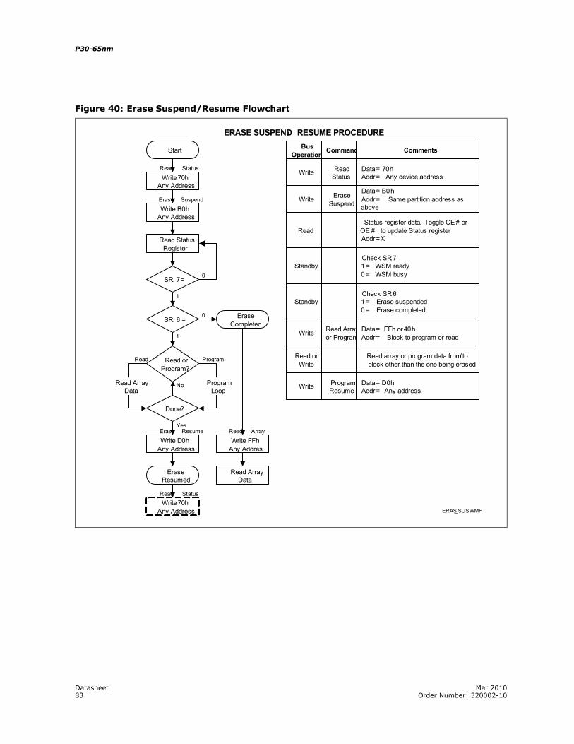
Datasheet Mar 201083 Order Number: 320002-10
P30-65nm
Figure 40: Erase Suspend/Resume Flowchart
Erase Completed
Read Array Data
0
0
No
Read
1
Program
ProgramLoop
Read ArrayData
1
Yes
Start
Read Status Register
SR. 7 =
SR. 6 =
Erase Resumed
Read or Program?
Done?
Write
Write
Standby
Standby
Write
Erase Suspend
Read Arrayor Program
Program Resume
Data = B0hAddr = Same partition address as above
Data = FFh or 40hAddr = Block to program or read
Check SR.71 = WSM ready0 = WSM busy
Check SR.61 = Erase suspended0 = Erase completed
Data = D0hAddr = Any address
Bus Operation Command Comments
ReadStatus register data. Toggle CE# or
OE # to update Status registerAddr =X
Read orWrite
Read array or program data from/ to block other than the one being erased
ERASE SUSPEND / RESUME PROCEDURE
ERAS_SUS.WMF
Write B0hAny Address
Erase Suspend
Write 70hAny Address
Read Status
Write D0hAny Address
Erase Resume
Write 70hAny Address
Read Status
Write FFhAny Addres
Read Array
Write Read Status
Data = 70hAddr = Any device address
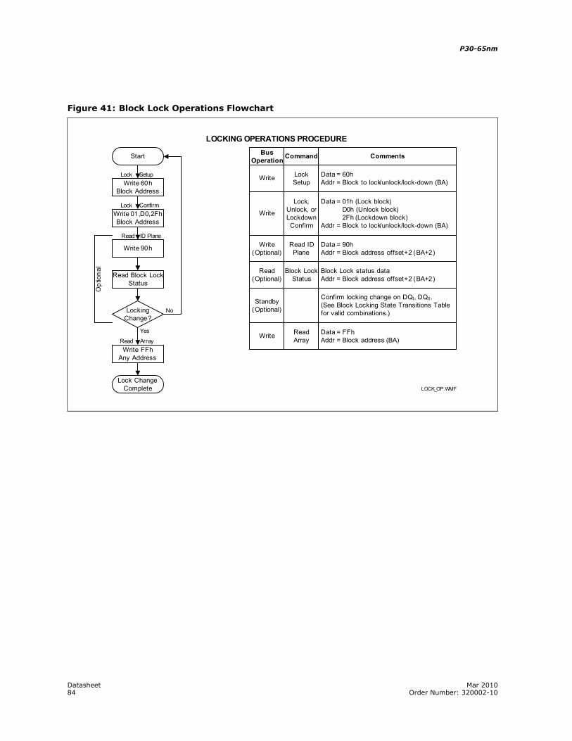
P30-65nm
Datasheet Mar 201084 Order Number: 320002-10
Figure 41: Block Lock Operations Flowchart
No
Op
tion
al
Start
Write 60hBlock Address
Write 90h
Read Block Lock Status
Locking Change?
Lock Change Complete
Write 01,D0,2FhBlock Address
Write FFhAny Address
Yes
Write
Write
Write(Optional)
Read(Optional)
Standby(Optional)
Write
LockSetup
Lock, Unlock, or Lockdown Confirm
Read ID Plane
Block Lock Status
Read Array
Data = 60hAddr = Block to lock/unlock/lock-down (BA)
Data = 01h (Lock block)D0h (Unlock block)2Fh (Lockdown block)
Addr = Block to lock/unlock/lock-down (BA)
Data = 90hAddr = Block address offset +2 (BA+2)
Block Lock status data Addr = Block address offset +2 (BA+2)
Confirm locking change on DQ1, DQ0.(See Block Locking State Transitions Table for valid combinations.)
Data = FFhAddr = Block address (BA)
Bus Operation Command Comments
LOCKING OPERATIONS PROCEDURE
LOCK_OP.WMF
Lock Confirm
Lock Setup
Read ID Plane
Read Array
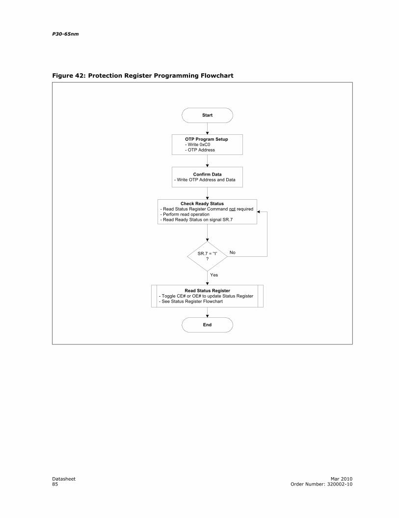
Datasheet Mar 201085 Order Number: 320002-10
P30-65nm
Figure 42: Protection Register Programming Flowchart
Start
Confirm Data - Write OTP Address and Data
Yes
SR.7 = '1'?
End
No
Read Status Register - Toggle CE# or OE# to update Status Register - See Status Register Flowchart
OTP Program Setup- Write 0xC0- OTP Address
Check Ready Status - Read Status Register Command not required - Perform read operation - Read Ready Status on signal SR.7
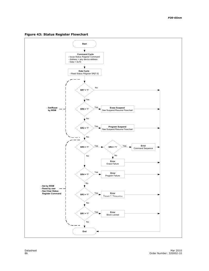
P30-65nm
Datasheet Mar 201086 Order Number: 320002-10
Figure 43: Status Register Flowchart
Start
SR7 = '1'
SR2 = '1'
SR4 = '1'
SR3 = '1'
SR1 = '1'
Yes
Yes
No
Yes
No
No
No
SR6 = '1'Yes
No
SR5 = '1'
No
No
Program SuspendSee Suspend /Resume Flowchart
Erase SuspendSee Suspend /Resume Flowchart
ErrorCommand Sequence
Yes
Yes
Yes
ErrorErase Failure
ErrorProgram Failure
ErrorVPEN/PP < VPENLK/PPLK
ErrorBlock Locked
- Set by WSM- Reset by user- See Clear Status
Register Command
- Set/Resetby WSM
SR4 = '1' Yes
No
End
Command Cycle- Issue Status Register Command- Address = any device address- Data = 0x70
Data Cycle- Read Status Register SR[7:0]
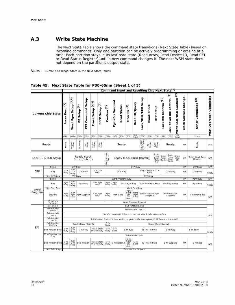
Datasheet Mar 201087 Order Number: 320002-10
P30-65nm
A.3 Write State Machine
The Next State Table shows the command state transitions (Next State Table) based on incoming commands. Only one partition can be actively programming or erasing at a time. Each partition stays in its last read state (Read Array, Read Device ID, Read CFI or Read Status Register) until a new command changes it. The next WSM state does not depend on the partition’s output state.
Note: IS refers to Illegal State in the Next State Tables
Table 45: Next State Table for P30-65nm (Sheet 1 of 3)Command Input and Resulting Chip Next State(1)
Current Chip State
Arr
ay R
ead
(3
)
Wo
rd P
gm
Setu
p (
4,9
)
BP
Setu
p (
8)
EFI
Co
mm
an
d S
etu
p
Era
se S
etu
p (
4,9
)
BE
FP
Setu
p (
6)
Co
nfi
rm (
7)
Pg
m/
Ers
Su
spen
d
Read
Sta
tus
Cle
ar
SR
(5
)
Read
ID
/Q
uery
Lo
ck/
RC
R/
EC
R S
etu
p
Bla
nk C
heck
OT
P S
etu
p
Lo
ck B
lk C
on
firm
(7
)
Lo
ck-d
ow
n B
lk C
on
firm
(7
)
Wri
te E
CR
/R
CR
Co
nfi
rm (
7)
Blo
ck A
dd
ress
Ch
an
ge
Oth
er
Co
mm
an
ds
(2)
WS
M O
pera
tio
n C
om
ple
tes
(FFh) (40h) (E8h) (EBh) (20h) (80h) (D0h) (B0) (70h) (50h) (90h, 98h) (60h) (BCh) (C0h) (01h) (2Fh) (03h,
04h) other
Ready
Rea
dy
Progra
mSet
up
BP S
etup
EFI
Set
up
Era
seSet
up
BEFP
Set
up
ReadyLo
ck/R
CR
/ECR S
etup
BC
Set
up
OTP
Set
up
Ready N/A
Rea
dy
N/A
Lock/RCR/ECR Setup Ready (LockError [Botch])
Rea
dy
(Unlo
ckBlo
ck)
Ready (Lock Error [Botch])Ready (Lock Error [Botch])
Ready (Lock Block)
Ready (Lock down Block)
Ready (Set CR)
N/A Ready (Lock Error [Botch]) N/A
OTP
Setup OTP Busy OTP Busy N/A OTP Busy N/A
Busy OTP Busy
IS in OTP Busy
OTP Busy IS in OTP Busy OTP Busy Illegal State in OTP
Busy OTP Busy N/A OTP BusyReady
IS in OTP Busy OTP Busy OTP Busy
Word Program
Setup Word Program Busy N/A Pgm Busy N/A
Busy Pgm Busy
IS in Pgm Busy
Pgm Busy IS in Pgm Busy
Pgm Busy
Pgm Susp Word Pgm Busy IS in Word Pgm Busy Word Pgm Busy N/A Pgm Busy
Ready
IS in Pgm Busy Word Pgm Busy
Suspend Pgm Susp
IS in Pgm Susp
Pgm Suspend IS in Pgm Susp
Pgm Busy Pgm Susp
Pgm Susp (Er bits
clear)
Word Pgm Susp
Illegal State in Pgm Suspend
Word Program Suspend N/A Word Pgm Susp
N/A
IS in Pgm Suspend Word Program Suspend
EFI
EFI Setup Sub-function Setup
N/A
Sub-function Setup Sub-op-code Load 1
Sub-op-codeLoad 1 Sub-function Load 2 if word count >0, else Sub-function confirm
Sub-functionLoad 2 Sub-function Confirm if data load in program buffer is complete, ELSE Sub-function Load 2
Sub-function Confirm Ready (Error [Botch]) S-fn
Busy Ready (Error [Botch])
Sub-function Busy S-fn Busy
IS in S-fn Busy
S-fn Busy Illegal State in S-fn Busy
S-fn Busy
S-fn Susp S-fn Busy IS in S-fn Busy S-fn Busy S-fn Busy
ReadyIS in Sub-function
Busy Sub-function Busy
Sub-function Susp S-fn Susp
IS in S-fn Susp
Sub-function Illegal State in S-fn Busy
S-fn Busy S-fn Suspend
S-fn Susp (Er bits
clear)
S-fn Susp IS in S-fn Susp S-fn Suspend N/A S-fn Susp
N/A
IS in S-fn Susp Sub-function Suspend
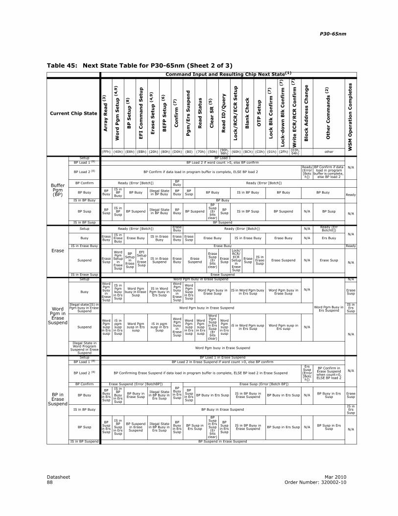
P30-65nm
Datasheet Mar 201088 Order Number: 320002-10
Buffer Pgm (BP)
Setup BP Load 1
N/ABP Load 1 (8) BP Load 2 if word count >0, else BP confirm
BP Load 2 (8) BP Confirm if data load in program buffer is complete, ELSE BP load 2Ready (Error [Botch])
BP Confirm if data load in program
buffer is complete, else BP load 2
BP Confirm Ready (Error [Botch]) BP Busy Ready (Error [Botch])
BP Busy BP Busy
IS in BP
BusyBP Busy Illegal State
in BP BusyBP
BusyBP
Susp BP Busy IS in BP Busy BP Busy BP BusyReady
IS in BP Busy BP Busy
BP Susp BP Susp
IS in BP
SuspBP Suspend Illegal State
in BP BusyBP
Busy BP Suspend
BP Susp (Er bits
clear)
BP Susp IS in BP Susp BP Suspend N/A BP Susp
N/A
IS in BP Susp BP Suspend
Erase
Setup Ready (Error [Botch]) Erase Busy Ready (Error [Botch]) N/A Ready (Err
Botch0])N/A
Busy Erase Busy
IS in Erase Busy
Erase Busy IS in Erase Busy
Erase Busy
Erase Susp Erase Busy IS in Erase Busy Erase Busy N/A Ers Busy
IS in Erase Busy Erase Busy Ready
Suspend Erase Susp
Word Pgm
Setup in
Erase Susp
BP Setup
in Erase Susp
EFI Setup
in Erase Susp
IS in Erase Suspend
Erase Busy
Erase Suspend
Erase Susp (Er bits
clear)
Erase Susp
Lock/RCR/ECR
Setup in
Erase Susp
Erase Susp
IS in Erase Susp
Erase Suspend N/A Erase SuspN/A
IS in Erase Susp Erase Suspend
Word Pgm in Erase
Suspend
Setup Word Pgm busy in Erase Suspend
N/A
Word Pgm Busy in Ers Suspend
N/A
Busy
Word Pgm busy
in Erase Susp
IS in Pgm busy in Ers Susp
Word Pgm busy in Erase
Susp
IS in Word Pgm busy in
Ers Susp
Word Pgm busy
in Erase Susp
Word Pgm Susp in Ers Susp
Word Pgm busy in Erase Susp
IS in Word Pgm busy in Ers Susp
Word Pgm busy in Erase Susp
Erase Susp
Illegal state(IS) in Pgm busy in Erase
SuspendWord Pgm busy in Erase Suspend
IS in Ers
Susp
Suspend
Word Pgm susp in Ers susp
iS in pgm susp in Ers Susp
Word Pgm susp in Ers
susp
iS in pgm susp in Ers
Susp
Word Pgm busy
in Erase Susp
Word Pgm susp in Ers susp
Word Pgm susp in Ers susp
Word Pgm Susp in Ers Susp (Er bits
clear)
Word Pgm susp in Ers susp
iS in Word Pgm susp in Ers Susp
Word Pgm susp in Ers susp N/A
N/A
Illegal State in Word Program
Suspend in Erase Suspend
Word Pgm busy in Erase Suspend
BP in Erase
Suspend
Setup BP Load 1 in Erase Suspend
N/A
BP Load 1 (8) BP Load 2 in Erase Suspend if word count >0, else BP confirm
BP Load 2 (8) BP Confirming Erase Suspend if data load in program buffer is complete, ELSE BP load 2 in Erase Suspend
Ers Susp (Error [Botch])
BP Confirm in Erase Suspend when count=0, ELSE BP load 2
BP Confirm Erase Suspend (Error [BotchBP])BP
Busy in Ers Susp
Erase Susp (Error [Botch BP])
BP BusyBP
Busy in Ers Susp
IS in BP
Busy in Ers Susp
BP Busy in Erase Susp
Illegal State in BP Busy in
Ers Susp
BP Susp in Ers Susp
BP Busy in Ers Susp IS in BP Busy in Erase Suspend BP Busy in Ers Susp N/A BP Busy in Ers
SuspErase Susp
IS in BP Busy BP Busy in Erase SuspendIS in Ers
Susp
BP SuspBP
Susp in Ers Susp
IS in BP
Susp in Ers Susp
BP Suspend in Erase Suspend
Illegal State in BP Busy in
Ers Susp
BP Busy in Ers Susp
BP Susp in Ers Susp
BP Susp in Ers Susp (Er bits
clear)
BP Susp in Ers Susp
IS in BP Busy in Erase Suspend BP Susp in Ers Susp N/A BP Susp in Ers
Susp N/A
IS in BP Suspend BP Suspend in Erase Suspend
Table 45: Next State Table for P30-65nm (Sheet 2 of 3)Command Input and Resulting Chip Next State(1)
Current Chip State
Arr
ay R
ead
(3
)
Wo
rd P
gm
Setu
p (
4,9
)
BP
Setu
p (
8)
EFI
Co
mm
an
d S
etu
p
Era
se S
etu
p (
4,9
)
BE
FP
Setu
p (
6)
Co
nfi
rm (
7)
Pg
m/
Ers
Su
spen
d
Read
Sta
tus
Cle
ar
SR
(5
)
Read
ID
/Q
uery
Lo
ck/
RC
R/
EC
R S
etu
p
Bla
nk C
heck
OT
P S
etu
p
Lo
ck B
lk C
on
firm
(7
)
Lo
ck-d
ow
n B
lk C
on
firm
(7
)
Wri
te E
CR
/R
CR
Co
nfi
rm (
7)
Blo
ck A
dd
ress
Ch
an
ge
Oth
er
Co
mm
an
ds
(2)
WS
M O
pera
tio
n C
om
ple
tes
(FFh) (40h) (E8h) (EBh) (20h) (80h) (D0h) (B0) (70h) (50h) (90h, 98h) (60h) (BCh) (C0h) (01h) (2Fh) (03h,
04h) other
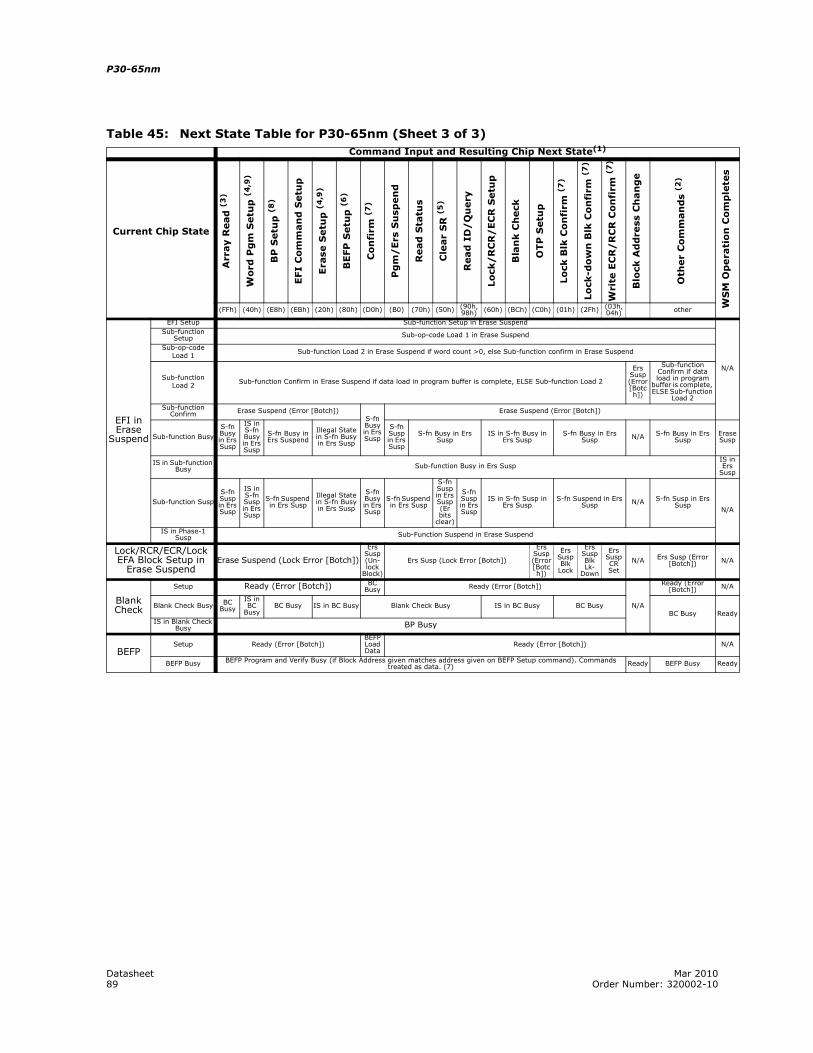
Datasheet Mar 201089 Order Number: 320002-10
P30-65nm
EFI in Erase
Suspend
EFI Setup Sub-function Setup in Erase Suspend
N/A
Sub-function Setup Sub-op-code Load 1 in Erase Suspend
Sub-op-codeLoad 1 Sub-function Load 2 in Erase Suspend if word count >0, else Sub-function confirm in Erase Suspend
Sub-functionLoad 2 Sub-function Confirm in Erase Suspend if data load in program buffer is complete, ELSE Sub-function Load 2
Ers Susp (Error [Botch])
Sub-function Confirm if data load in program
buffer is complete, ELSE Sub-function
Load 2Sub-function
Confirm Erase Suspend (Error [Botch])S-fn Busy in Ers Susp
Erase Suspend (Error [Botch])
Sub-function Busy
S-fn Busy in Ers Susp
IS in S-fn Busy in Ers Susp
S-fn Busy in Ers Suspend
Illegal State in S-fn Busy in Ers Susp
S-fn Susp in Ers Susp
S-fn Busy in Ers Susp
IS in S-fn Busy in Ers Susp
S-fn Busy in Ers Susp N/A S-fn Busy in Ers
SuspErase Susp
IS in Sub-function Busy Sub-function Busy in Ers Susp
IS in Ers
Susp
Sub-function SuspS-fn Susp in Ers Susp
IS in S-fn Susp in Ers Susp
S-fn Suspend in Ers Susp
Illegal State in S-fn Busy in Ers Susp
S-fn Busy in Ers Susp
S-fn Suspend in Ers Susp
S-fn Susp in Ers Susp (Er bits
clear)
S-fn Susp in Ers Susp
IS in S-fn Susp in Ers Susp
S-fn Suspend in Ers Susp N/A S-fn Susp in Ers
SuspN/A
IS in Phase-1 Susp Sub-Function Suspend in Erase Suspend
Lock/RCR/ECR/Lock EFA Block Setup in
Erase SuspendErase Suspend (Lock Error [Botch])
Ers Susp (Un-lock
Block)
Ers Susp (Lock Error [Botch])
Ers Susp (Error [Botch])
Ers Susp Blk
Lock
Ers Susp Blk Lk-
Down
Ers Susp CR Set
N/A Ers Susp (Error [Botch]) N/A
Blank Check
Setup Ready (Error [Botch]) BC Busy Ready (Error [Botch])
N/A
Ready (Error [Botch]) N/A
Blank Check Busy BC Busy
IS in BC
BusyBC Busy IS in BC Busy Blank Check Busy IS in BC Busy BC Busy
BC Busy ReadyIS in Blank Check
Busy BP Busy
BEFPSetup Ready (Error [Botch])
BEFP Load Data
Ready (Error [Botch]) N/A
BEFP Busy BEFP Program and Verify Busy (if Block Address given matches address given on BEFP Setup command). Commands treated as data. (7) Ready BEFP Busy Ready
Table 45: Next State Table for P30-65nm (Sheet 3 of 3)Command Input and Resulting Chip Next State(1)
Current Chip StateA
rray R
ead
(3
)
Wo
rd P
gm
Setu
p (
4,9
)
BP
Setu
p (
8)
EFI
Co
mm
an
d S
etu
p
Era
se S
etu
p (
4,9
)
BE
FP
Setu
p (
6)
Co
nfi
rm (
7)
Pg
m/
Ers
Su
spen
d
Read
Sta
tus
Cle
ar
SR
(5
)
Read
ID
/Q
uery
Lo
ck/
RC
R/
EC
R S
etu
p
Bla
nk C
heck
OT
P S
etu
p
Lo
ck B
lk C
on
firm
(7
)
Lo
ck-d
ow
n B
lk C
on
firm
(7
)
Wri
te E
CR
/R
CR
Co
nfi
rm (
7)
Blo
ck A
dd
ress
Ch
an
ge
Oth
er
Co
mm
an
ds
(2)
WS
M O
pera
tio
n C
om
ple
tes
(FFh) (40h) (E8h) (EBh) (20h) (80h) (D0h) (B0) (70h) (50h) (90h, 98h) (60h) (BCh) (C0h) (01h) (2Fh) (03h,
04h) other
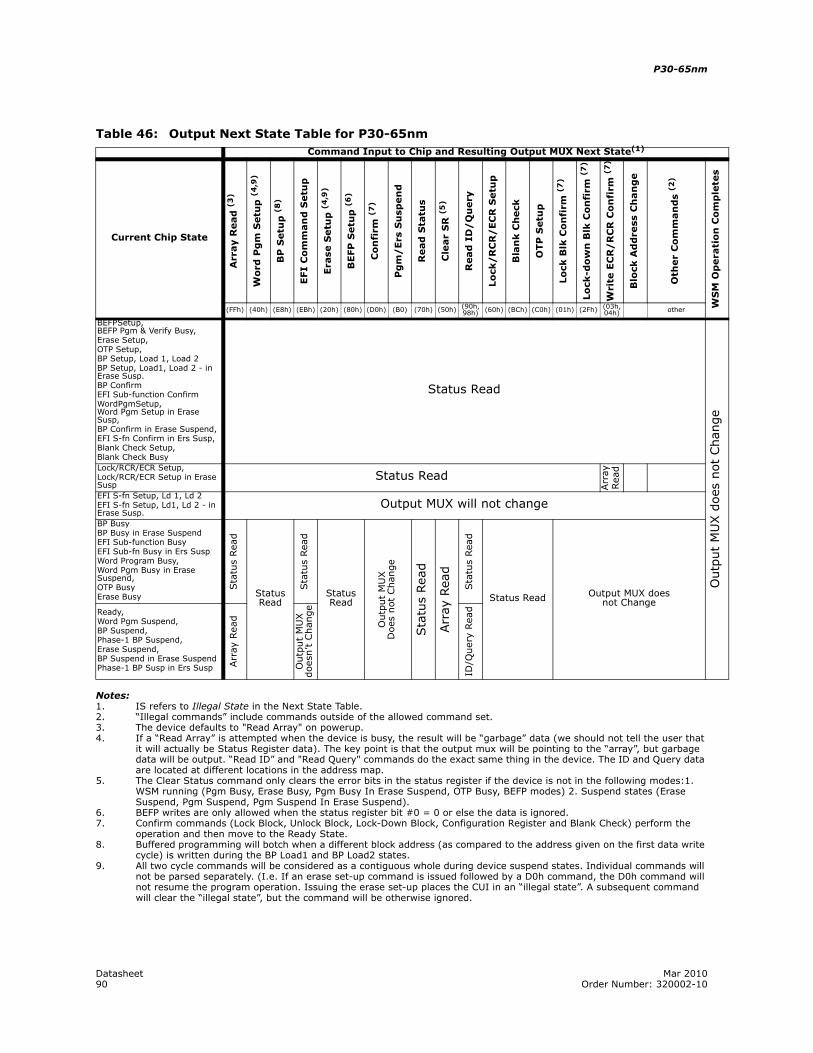
P30-65nm
Datasheet Mar 201090 Order Number: 320002-10
Notes:1. IS refers to Illegal State in the Next State Table.2. “Illegal commands” include commands outside of the allowed command set.3. The device defaults to "Read Array" on powerup.4. If a “Read Array” is attempted when the device is busy, the result will be “garbage” data (we should not tell the user that
it will actually be Status Register data). The key point is that the output mux will be pointing to the “array”, but garbage data will be output. “Read ID” and "Read Query" commands do the exact same thing in the device. The ID and Query data are located at different locations in the address map.
5. The Clear Status command only clears the error bits in the status register if the device is not in the following modes:1. WSM running (Pgm Busy, Erase Busy, Pgm Busy In Erase Suspend, OTP Busy, BEFP modes) 2. Suspend states (Erase Suspend, Pgm Suspend, Pgm Suspend In Erase Suspend).
6. BEFP writes are only allowed when the status register bit #0 = 0 or else the data is ignored.7. Confirm commands (Lock Block, Unlock Block, Lock-Down Block, Configuration Register and Blank Check) perform the
operation and then move to the Ready State.8. Buffered programming will botch when a different block address (as compared to the address given on the first data write
cycle) is written during the BP Load1 and BP Load2 states.9. All two cycle commands will be considered as a contiguous whole during device suspend states. Individual commands will
not be parsed separately. (I.e. If an erase set-up command is issued followed by a D0h command, the D0h command will not resume the program operation. Issuing the erase set-up places the CUI in an “illegal state”. A subsequent command will clear the “illegal state”, but the command will be otherwise ignored.
Table 46: Output Next State Table for P30-65nmCommand Input to Chip and Resulting Output MUX Next State(1)
Current Chip StateA
rray R
ead
(3
)
Wo
rd P
gm
Setu
p (
4,9
)
BP
Setu
p (
8)
EFI
Co
mm
an
d S
etu
p
Era
se S
etu
p (
4,9
)
BE
FP
Setu
p (
6)
Co
nfi
rm (
7)
Pg
m/
Ers
Su
spen
d
Read
Sta
tus
Cle
ar
SR
(5
)
Read
ID
/Q
uery
Lo
ck/
RC
R/
EC
R S
etu
p
Bla
nk C
heck
OT
P S
etu
p
Lo
ck B
lk C
on
firm
(7
)
Lo
ck-d
ow
n B
lk C
on
firm
(7
)
Wri
te E
CR
/R
CR
Co
nfi
rm (
7)
Blo
ck A
dd
ress
Ch
an
ge
Oth
er
Co
mm
an
ds
(2)
WS
M O
pera
tio
n C
om
ple
tes
(FFh) (40h) (E8h) (EBh) (20h) (80h) (D0h) (B0) (70h) (50h) (90h, 98h) (60h) (BCh) (C0h) (01h) (2Fh) (03h,
04h) other
BEFP Setup, BEFP Pgm & Verify Busy, Erase Setup, OTP Setup, BP Setup, Load 1, Load 2BP Setup, Load1, Load 2 - in Erase Susp.BP ConfirmEFI Sub-function ConfirmWord Pgm Setup, Word Pgm Setup in Erase Susp,BP Confirm in Erase Suspend,EFI S-fn Confirm in Ers Susp,Blank Check Setup,Blank Check Busy
Status Read
Outp
ut
MU
X d
oes
not
Chan
ge
Lock/RCR/ECR Setup, Lock/RCR/ECR Setup in Erase Susp
Status Read
Arr
ayRead
EFI S-fn Setup, Ld 1, Ld 2EFI S-fn Setup, Ld1, Ld 2 - in Erase Susp.
Output MUX will not change
BP BusyBP Busy in Erase SuspendEFI Sub-function BusyEFI Sub-fn Busy in Ers SuspWord Program Busy,Word Pgm Busy in Erase Suspend,OTP BusyErase Busy
Sta
tus
Rea
d
Status Read
Sta
tus
Rea
d
Status Read
Outp
ut
MU
XD
oes
not
Change
Sta
tus
Rea
d
Arr
ay R
ead
Sta
tus
Rea
d
Status Read Output MUX doesnot Change
Ready,Word Pgm Suspend,BP Suspend,Phase-1 BP Suspend,Erase Suspend,BP Suspend in Erase SuspendPhase-1 BP Susp in Ers Susp A
rray
Read
Outp
ut
MU
Xdoes
n’t C
hange
ID/Q
uery
Read
Datasheet Mar 201091 Order Number: 320002-10
P30-65nm
Appendix B Conventions - Additional Information
B.1 Conventions
B.2 Acronyms
VCC: Signal or voltage connection
VCC: Signal or voltage level
0x: Hexadecimal number prefix
h: Hexadecimal number suffix
0b: Binary number prefix
SR.4: Denotes an individual register bit.
A[15:0]: Denotes a group of similarly named signals, such as address or data bus.
A5: Denotes one element of a signal group membership, such as an individual address bit.
Bit: Binary unit
Byte: Eight bits
Word: Two bytes, or sixteen bits
Kbit: 1024 bits
KByte: 1024 bytes
KWord: 1024 words
Mbit: 1,048,576 bits
MByte: 1,048,576 bytes
MWord: 1,048,576 words
BEFP: Buffer Enhanced Factory Programming
CFI: Common Flash Interface
MLC: Multi-Level Cell
OTP: One-Time Programmable
PLR: Protection Lock Register
PR: Protection Register
RCR: Read Configuration Register
RFU: Reserved for Future Use
SR: Status Register
WSM: Write State Machine
SRD Status Register Data
CUI Command User Interface
EFI Extended Function Interface
PAD Password Access Data
P30-65nm
Datasheet Mar 201092 Order Number: 320002-10
B.3 Nomenclature
Block : A group of bits, bytes, or words within the flash memory array that erase simultaneously. The P30-65nm has two block sizes: 32 KByte and 128 KByte.
Main block : An array block that is usually used to store code and/or data. Main blocks are larger than parameter blocks.
Parameter block : An array block that may be used to store frequently changing data or small system parameters that traditionally would be stored in EEPROM.
Top parameter device : A device with its parameter blocks located at the highest physical address of its memory map.
Bottom parameter device : A device with its parameter blocks located at the lowest physical address of its memory map.
Datasheet Mar 201093 Order Number: 320002-10
P30-65nm
Appendix C Revision History
Revision Date Revision Description
Mar 2010 10
Program performance update in front page, Section 29, “Program and Erase Specifications” and CFI.tDVWH specification comments, Table 28, “AC Write Specifications” on page 59.Erase/program suspend latency specification update, Table 29, “Program and Erase Specifications” on page 63. Leaded TSOP part EOL. Burst latency update and 40MHz spec update, Table 16, “LC and Frequency Support” on page 42.Clarify the capacitance, Table 26, “Capacitance” on page 54.Ordering Information update.
Aug 2009 09
QUAD+ ball height correction to 0.2mm in Figure 4. Update the Block lock Operations, Program Suspend/Resume, Erase Suspend/Resume flowcharts in Figure 41, Figure 36, Figure 40, backward compatible with 130nm.Align the sequence error description in Table 14. Add TSOP 40MHz Burst Spec in Table 27, “AC Read Specifications”. Add note 7 in buffer program flowchart Figure 37.Update VIL undershoot and overshoot of Note 2 in Table 24.Update CFI 0x2A data in Table 37, “Device Geometry Definition”.
Apr 2009 08
Add 512 Mbit (256/256) memory map in Figure 1, “P30-65nm Memory Map” on page 7Update QUAD+ signal description by changing A25 into RFU in Figure 8, “QUAD+ SCSP Ballout and Signals” on page 15.Correct RCR.4, RCR.5, RCR.7 and RCR.9 definitions in Table 15, “Read Configuration Register Description” on page 39.Correct A0 to A1 signal naming and remove invalid x8 information in Table 33, “Example of CFI Structure Output of x16 Devices” on page 67.
Jan 2008 07
Update QUAD+ package ballout H8 from OE# to F2-OE#. See Figure 8, “QUAD+ SCSP Ballout and Signals” on page 15.Update QUAD+ Signal Description A[MAX:1] to A[MAX:0] and its Name and Function. See Figure 6, “QUAD+ SCSP Signal Descriptions” on page 17.Update Virtual Chip Enable Description from Address 25 to the maximum address bit. See Section 1.3, “Virtual Chip Enable Description” on page 6.Update TSOP Pinout P13 from VCC to RFU. See Section 6, “56-Lead TSOP Pinout (256-Mbit)” on page 13.Complete Section 9.2, “Blank Check” on page 33. Minor wording modifications.
Dec 2008 06
Correct page buffer address bit to Four on Section 7.1, “Asynchronous Page-Mode Read” .Correct VHH to VPPH on Table 23, “DC Current Characteristics” on page 51 note 7.
Nov 2008 05
Remove 128M related contents;Return to StrataFlash trademark;Update the buffer program for cross 512-Word boundary;Correct A24 to A25 for virtual CE description in section 1.3;Remove Numonyx Confidential.
Nov 2008 04Update Buffer program flowchart same as 130nm;Minor wording modifications.
Sep 2008 03Update new trademark Axcell;Remove 64M related contents.
July 2008 02
Add W28 AC specification;Fix Buffered Program Command error in figure 38;Update block locking state diagram;Update Address range in Memory Map figure;Change LSB Address in ballout and pinout description from A0 back to A1 to match P30 130nm.

P30-65nm
Datasheet Mar 201094 Order Number: 320002-10
May 2008 01 Initial Release
Revision Date Revision Description