numerical simulation of thick line width measurements by reflected
TRANSCRIPT

Numerical Simulation of Thick Line Width Measurements by Reflected Light
Gregory L Wojcik, John Mould, Jr.Weidlinger Associates, Los Altos, CA 94022
Robert J. Monteverdet, Jaroslav J. ProchazkaVLSI Standards, Mt. View, CA 94943
John R. Frank, Jr.SEMATECH, Austin, TX 78741
ABSTRACr
IC fabrication problems grow as nominal feature sizes shrink, due in large part to fundamental opticaldiffraction limits. Currently, one of the most pressing needs is robust critical dimension measurement.However, optical methods must be refined for this scale of submicron metrology, particularly in the case ofthick features. This paper examines the problem of reflected light microscopy for nominal I micron highlines on silicon using 2-D, time-domain finite element simulations. The experimental basis is a prototypeline width standard that is characterized using optical, contact, and SEM measurements. Microscope andsimulated images are compared for 1 and 3 micron wide lines. Good "1st order" correlation is found betweenreal and synthetic images but model uncertainties need to be reduced and microscope aberrations need to bequantified before "2'' order" differences can be eliminated. Numerical experiments are used to: relateimages to resonance patterns in the feature; determine the strength of evanescent waves near the line; andcontrast isolated and periodic line images as a function of pitch.
1. INTRODUCTION
Each new generation of integrated circuit technology achieves an increase in device density byfractionally reducing feature size. Today nominal IC features are under one micron and will be one-halfmicron in the near future. However, as characteristic dimensions have shrunk, fabrication and qualitycontrol problems have grown substantially. In large part this is because the optical wavelengths used inprocessing and inspection are 1/2 to 1/3 of the feature size, hence fundamental diffraction limits are beingapproached. Such limits reduce our degree of confidence in the proper corrective action needed to resolvethese fabrication and quality control problems. Part of the short-term solution is more robust processmonitoring by on-line critical dimension (CD) measurement.
Op tical metrology may continue to provide an effective basis for CD measurement, but, the resolutionlimit of conventional optics and complex proximity effects raise serious questions about submicron accuracy.This is especially true for thick lines, i.e., those with comparable height, width, and illuminationwavelength. Accuracy capabilities must be established and useful thresholding and calibration(correlation) criteria devised if optical metrology is to remain viable and complement alternativetechniques like scanning electron microscopy. This paper examines the problem of accurate thick linemeasurement by comparing numerical simulation, optical imaging, and SEM imaging of a prototypecalibration standard manufactured by VLSI Standards, Inc. Calibration of existing systems by means of areliable thick line/substrate standard (comparator) is a first step towards enhanced optical accuracy.
By way of background, various forms of microscopy currently dominate modern IC metrology.Conventional imaging by visible light has been the mainstay and is still common by virtue of noninvasiveoperation, high throughput, and the large installed equipment base. Enhancements like confocal andcoherence probe methods are attempting to extend functionality. Despite technical complexities, scanningelectron microscopy (SEM) is now a practical alternative by virtue of lower voltages and full automation.More exotic scanning probe methods exist and show promise, but are currently of limited utility for generalfeatures. Electrical test probes provide an alternative to microscopy, albeit for cross-sectional area ofdedicated conducting structures rather than dimensional images of arbitrary features.
tNow at KLA Instruments Corp., Santa Clara, CA 95052
0-8194-0563-9/91/$4.00 SPIE Vol. 1464 Integrated Circuit Metrology, Inspection, and Process Control V (1991) / 187

Considering the breadth of technologies available for submicron metrology, it is clear that optics willface stiff competition in the future, particularly as SEM methods are made more efficient. The question iswhether optical microscopy will eventually be dedicated to overlay measurements only, or limited tolarger CDs (e.g., >0.7 microns), or whether enhancements will allow it to maintain some metrology utilityin conjunction with other technologies. The issue comes down to that of accuracy, i.e., on the ability offuture optical systems to provide absolute dimensional measurements of submicron features. The answer isin the hands of instrument makers and probably depends on their ability to incorporate complete andpractical phase information into a complex image of the object, rather than merely offering intensityimages at a reduced wavelength or with greater depth of focus.
To determine whether optical enhancements are indeed practical, renewed attention to the effectiveuse of optical microscopy is called for, particularly with regards to measurements of thick lines andfeatures on topographically complex substrates. Such research is very difficult to perform experimentallybecause of object size and the requisite parameter variations, as well as sundry uncertainties in fabricatedgeometry and optical system aberrations. On the other hand, numerical simulation, i.e., modeling andanalysis, provides a practical way to investigate the problem. Numerical experiments can fully accountfor the vector wave nature of light while accommodating multi-dimensional model geometries, and theresulting opticai resonances and edge effects that complicate today's imaging.
Although analysis by some form of numerical simulation is not new in optics, it has only been appliedto metrology over the last decade. Some of the first work was done by Nyyssonen and coworkers, e.g., [1],[2], and more recently by Yuan and Strojwas [3], utilizing the so-called waveguide model of periodicdiffractors to simulate scattering from 2-D structures. An alternative to this semi-analytical approach is adiscrete numerical algorithm like the finite difference or finite element method in either the frequency- ortime-domain. Discrete time-domain codes were successfully applied by Wojcik, et al. [4] to submicronparticulate scattering problems associated with IC surface contamination and sensor calibration. Thesemethods are new to optics but have proven their worth in other branches of engineering and appliedphysics, and offer a robust alternative that is relatively unfettered by geometrical constraints. Usingeither formal or informal inversion techniques they provide a means to actually verify feature cross-sections from image data.
Discrete numerical algorithms offer the advantage of geometric generality but with the disadvantageof requiring extensive number crunching. Fortunately, current workstations make all but the mostcomputationally intensive algorithms practical. For example, calculations that had to be done remotely ona Cray 2 in 1987 for reasons of speed and memory can now be done on the newest IBM or Sun workstationswith better overall turnaróund time (calculation and post-processing time). The calculated images andscattering pictures described below take only fifteen minutes to execute and display on an IBM RS 6000, andthis time is easily reduced to a couple of minutes if only microscope images are simulated.
In this paper we explore a conventional reflected light microscopy problem on the basis of 2-D,time-domain finite element simulations. We characterize the sample using physical, optical, and SEMmeasurements and critically compare simulated and microscope images. Numerical experiments areperformed to: show what a microscope actually "sees" in terms of optical resonance patterns in the feature;determine the significance of evanescent waves; and compare isolated versus periodic models. This exerciseprovides a number of interesting insights into the problem of imaging and measuring thick featuresoptically and may suggest some of the directions and ground rules for future research and development.
2. THICK LINE SAMPLE AND IMAGING SYSTEM
Measurements are made on a thick-line calibration die developed by VLSI Standards. Except for filmthickness, the die is very similar to that described in [5]. The patterns are oxynitride on bare silicon andinclude lines, spaces, and pitches. The oxynitride is constituted to mimic the optical properties ofphotoresist but with better material stability. The lines have a nominal height of one micron and varyfrom one to five microns wide. At a wavelength of 0.546 microns, real parts of the refractive indices areapproximately 1.64 for the oxynitride and 4.1 for the silicon.
The measurement system consists of a tuned, bright field optical microscope for reflected light,modeled after a prototype instrument at NIST described by Nyyssonen [6]. Tuning includes realigned
188 / SPIE Vol. 1464 Integrated Circuit Metrology, Inspection, and Process Control V (1991)

optical elements, a stabilized platform, and piezoelectric replacing mechanical focusing. Illumination isessentially monochromatic at a wavelength of 0.546 microns (green light), provided by a narrowbandinterference filter (0.019 micron bandwidth) and mercury arc lamp. Illumination at the object exhibitshigh spatial coherence by virtue of a small condenser aperture, yielding a coherence factor of 0.2 (=condenser NA/objective NA). The numerical aperture of the imaging objective is 0.95. Polarization iscontrolled by a linear polarizing element in the illumination optics.
The image is an intensity scan across the line feature obtained by illuminating a photomultiplier tubethrough a scanning slit in the image plane. The slit integrates a 0.156 micron wide swath in the objectplane. A typical suite of measurements includes images at various levels of focus. The rule of thumb forbest focus is the level that produces sharpest contrast, i.e., highest gradient between maximum andminimum intensities near the "edge" of the feature. The quantitative criterion for choosing the "best focus"level is the one that minimizes distance between the principal maxima in the image. Image crossplotsfrom the I and 3 micron lines for TE (s-), TM (p..), and random (s + p) polarization are shown in Figure 1.Theoretically, the random polarization image should be a simple average of the TE and TM images, e.g.,[7].
An important aspect of the optical imaging system is its relative simplicity and modelability. Thisfacilitates comparisons between real and simulated (synthetic) images, and the actual feature. It iscritical in this paper to have a deterministic system as a control so that images can be calculated withreliable fidelity from numerical simulations. Note that the underlying assumption here is that once theline width has been calibrated by the control optical system, the CD standard can then be used tocalibrate the broadband optical systems commonly available in industry, which are typically moredifficult to model than our control system. However, to use the standard as an effective comparator,simulation is required to account for nuances in feature and substrate properties, and to insure correctinterpretation of results.
3. THE NUMERICAL MODEL
The numerical simulations are based on a rigorous finite element formulation of Maxwell's equations inthe time-domain over a small region around and including the scattering feature, i.e., the finite elementmodel. This model consists of a set of ordinary differential equations in time that result from the finiteelement semi-discretization of the spatial differential operator. Strong similarities exist between thisapproach and the finite difference method, e.g., [8]. An introductory description and comparison of thetechniques may be found in [4], although the current codes are much enhanced and optimized versions ofthose described. A more comprehensive description of the Galerkin finite element formulation used here isavailable in [9].
The system of ordinary differential equations representing Maxwell's equations is integrated forwardin time explicitly using a computationally efficient element-by-element algorithm. This approacheliminates the need to solve large implicit systems of linear equations but requires a time step smallerthan the shortest wave transit time across any element. We have found by comparison that such explicitsolutions are faster by nearly on order of magnitude than frequency domain solutions, and often requiremuch less storage. The relative efficiency for 3-D problems is higher and in fact this time-domainalgorithm is currently the only approach that makes 3-D modeling feasible on a routine basis.
Only steady-state solutions of Maxwell's equations are of interest for imaging. Using the time-domainapproach, one choice is to integrate the system to steady-state assuming a transient startup with zeroinitial conditions. An alternative is to initialize the model to the free-field steady-state solution (i.e.,without the scatterer) and then integrate the full system to steady-state from that point. This latterapproach is used here in order to optimize boundary conditions. The free-field solution is obtained from anauxiliary analytical solution of the finite element equations for the actual boundary discretization.Because the free-field initial conditions are inconsistent with the presence of the feature, at start-up thefull model produces a scattered field spreading directly from the feature and incident on the model'sexterior boundaries. An efficient radiation boundary condition based on unidirectional wave motion(paraxial approximation) removes the scattered field there while simultaneously applying the steadyincident field.
SPIE Vol. 1464 Integrated Circuit Metrology, Inspection, and Process Control V (1991)1 189

The numerical model is designed to propagate waves with negligible grid dispersion and domaintruncation errors. The model used for virtually all of the calculations presented here consists of a grid 12.0microns wide and 3.3 microns high partitioned into 720x226 elements as shown in Figure 2. Elements in theair and oxynitride are approximately 17 nanometers square. The silicon is represented by the lowest 0.32microns of elements. The region around the scattering feature is modeled by skewed elements in the figurebut generally only rectangular or stairstep approximations of the feature are considered in our calculations.The various numerical errors have been quantified by comparing finite element and exact solutions of Mie-type scattering problems for cylinders in free space. Very good agreement is obtained provided 15 or moreelements support the illumination wavelength. The evanescent waves caused by diffraction from sharpedges have also been calculated and compared to results from a new theory of vector wave diffraction [101.Agreement with the vector theory is excellent and it should be noted that no edge singularities aresupported in the electhc field for the TE polarized illumination considered here.
The electromagnetic field approximating the partially coherent, monochromatic incident light iscomposed of incoherent plane waves filling the symmetric cone of illumination. Only 2-D models areconsidered and cylindrical rather than conical illumination is assumed. For a coherence factor of 0.2, 3 and5 waves in the plane of incidence yield nearly identical results so only 3 are used. The adequacy of thisassumption will be considered later in the paper. The superposition of waves is essentially an integration,hence the incidence angles are located at the Gauss points (0°, of the cone's angular interval andweighted accordingly, rather than evenly distributed with equal weights.
The numerical solution is complete when steady-state is achieved on a plane just above the feature.The resulting field is converted to an image by means of scalar Fourier optics. Functional details of theimaging optics, to the extent known, are included in the optical transfer function. Important degrees offreedom of the imaging model include illumination coherence factor, defocus, numerical aperture,polarization, spherical aberration, and comatic aberration. All but spherical aberration and coma areknown for the system.
4. PHYSICAL MODEL CONSTRAINTS
There are many control parameters in the thick line imaging problem, each with its own measurementuncertainty and influence on the image. It is essential to begin the calibration process with the principalmodel and microscope parameters well-constrained, so as to minimize dimension of the space that must besampled. Our efforts have concentrated solely on line parameters. Imaging parameters, particularlymicroscope aberrations and limitations of scalar imaging theory, need to be quantified in follow-onresearch. A future goal is to develop a generic rule table of imaging parameters, to be customized by usersfor different microscopes.
We initially constrain refractive index and line height using ellipsometry and profilometry at sites onthe oxynitride film or margins surrounding the plasma etched patterns on bare silicon. Film thickness isfurther constrained by measurements of relative reflectivity and phase shift between bare silicon and theoxynitride film. These are the baseline measurements made by VLSI Standards in conjunction with opticalimaging. Subsequent to optical imaging the sample was measured at SEMATECH using SEM images forwidth/pitch determination and profilometry for oxynitride film thickness.
For the sample considered, ellipsometry gives a refractive index of 1.63 in the oxynitride film at themicroscope's illumination wavelength of 0.546 microns. Initial thickness measurements by the VLSIprofilometer yield a film height of 0.979±0.003 microns. Calculations of relative reflectivity and phaseshift for the film on silicon show that the measured values, 0.69±0.02 and 119°±4° respectively, aresatisfied by a height of 0.966 microns. This is 1.33% thinner than the profilometer thickness and may bedue to over-etching of the silicon, which would imply that the lines sit on a 0.013 micron silicon pedestal.Subsequent height measurements by a profilometer at SEMATECH gave a line thickness of 0.97±0.002microns, which argues against a significant pedestal.
The above measurements are essentially nondestructive. Using SEM imaging to further constrain linegeometry requires destructive preparation of the sample. This involves a coating of gold for line widthdetermination, and focused ion beam (FIB) milling to expose cross-sections for shape characterization. SEMimages of the nominal 1 and 3 micron lines and 4 micron pitch array are shown in Figure 3a,b,c. The first
190 / SPIE Vol. 1464 Integrated Circuit Metrology, Inspection, and Process Control V (1991)

two top-down views on the left indicate a uniform line width measured by the SEM's edge detectionalgorithm at 1.53 and 3.19 microns for the nominal 1 and 3 micron lines, respectively. The line's cross-section is exposed by FIB milling. Because the sample is mounted on a thick quartz substrate for handling,end-on views of the line cross-sections could not be obtained. Instead the sample was rotated to the extentpossible, yielding off-axis views approximately 35° above the horizontal. These are shown on the right inthe figure and indicate sides sloped about 8° from the vertical, with shape apparently uniform down theline. Note that the change from a smooth to rough surface near the milled edge is due to erosion of thegold coating by the FIB.
Since SEM images suffer their own set of uncertainties, they must be interpreted with care. In the caseof the off-axis viewing arrangement, electron chromatic variations, the nonuniform collection field, anddetector placement cause some illusory distortion of the features. These parallax effects are mostpronounced in views of the periodic lines, Fig. 3c, which appear to widen away from the milled edge, incontrast to the uniform width indicated by the top-down view. To confirm the SEM cross-section, thefocused ion beam was used to image the samples at the same off-axis arrangement. The heavier ions yielda relatively undistorted image (not shown) that indicates proportions and sideslope nearly identical to theSEM image cross-section.
In the case of the top-down views, the edge detection rule used by the SEM is only an approximation,particularly considering the significant side slope and gold coating. Therefore, accuracy of the SEM-measured line width is still difficult to assess, even to within 5%. Assuming profilometer thickness as theruler, widths were also calculated from height-to-width proportions of the off-axis cross-sections. Afteraccounting for the view angle, these only agreed to within 5% to 15% of the top-down measurements, andwith no consistency from line to line. Pitch measurements generally gave much better agreement to opticalmeasurement because they are relative rather than absolute.
5. REAL VERSUS SYNTHE11C IMAGES
We compare microscope and simulated images for our best guess at the thick line model, and illustratethe effects of certain parameters. This is a preliminary example of numerical calibration, essentially anad hoc inversion process. It involves repeated trial and error variations on the target parameters in thenumerical model until a best fit is achieved between measured and simulated images. The inversion can bemade more rigorous as well as automated using least squares optimization and image sensitivity matrices(Jacobians).
of the target parameters considered, primaries are width, sideslope, and defocus, and secondaries arespherical and comatic aberration. Since line height and refractive index are well-constrained by themeasurements they are not used as target parameters in this paper, although measurement uncertaintiescertainly justify minor variations. The two features examined are the nominal 1 micron and 3 micron lines.We only consider synthetic and measured images for TE (s-) polarized illumination, i.e., electric fieldparallel to the line's axis, or equivalently, perpendicular to its cross-section (the plane of incidence). Thisis chosen because of its scalar simplicity, requiring one calculation per plane wave rather than the twonecessary for random polarization (TE + TM). "Best focus" microscope images provide the basis for allcomparisons. The image, in units of volts, is rescaled so that its specular intensity away from the edge isnumerically equal to the reflectivity of silicon, and shifted horizontally to line up reasonably with thesymmetric synthetic data.
5.1 Three Micron LineResults for the 3 micron line are shown in Figure 4. The line cross-section is initially assumed to be
rectangular rather than trapezoidal, with a refractive index of 1.63 and height of 0.966 microns. Theminimum width that reasonably fits the measured image is 3.3 microns, shown against the data in Fig. 4a.Observe in this figure that the specular intensity (outer flat part of the image) is the reflectivity of baresilicon, the central plateau intensity is the reflectivity of a 0.966 oxynitnde layer on silicon, and theirratio is 0.69, the measured relative reflectance. Existence of this central plateau indicates that at 3 micronspacing, and probably down to 2 microns, the edges are effectively isolated, i.e., their images do notinterfere appreciably. Differences between real and synthetic images include the inner-maxima overshootand shape of the outer-minima, namely, narrowness and overshoot. Changes in the synthetic image as line
SPIE Vol. 1464 Integrated Circuit Metrology, Inspection, and Process Control V (1991) / 191

width is increased from 3.3 to 3.4 microns are shown in the crossplot of Fig. 4b, where the primary effect isto substantially decrease the outer-maxima.
Effects of defocus are illustrated in Fig. 4c,d for the rectangular 3.3 and 3.4 micron lines. Levels ofdefocus that produced the greatest contrast between outer-maxima and -minima are found to be about -0.75and -0.9 microns for the 3.3 and 3.4 micron lines respectively. This implies that "best focus" in the dataactually represents a focus level close to the bottom of the line. Defocus is seen to decrease and broadenthe outer-minima (with an inflection point near the minimum for 3.4 microns), increase the outer-maxima,either increase or decrease the inner-maxima, and consistently lower the central plateau (thus decreasingthe apparent relative reflectance). If we were to pick a best fit to the data in terms of rectangular linewidth, it would be the 3.4 micron line based on the fit from outer-maxima to outer-minima.
Since the SEM images clearly indicate a trapezoidal rather than rectangular cross-section, we showthe effect of 8° sideslope in Figure 4e,f. Based on measurements of the off-axis SEM view of the 3 micronline in Fig. 3, the model cross-section was assumed to have top and bottom widths of 3.19 and 3.48 microns,respectively. Comparing Fig. 4e to Fig. 4a,b for the rectangular 3.3 and 3.4 micron lines, we see strongsimilarities to the 3.3 micron line image despite the fact that the average width is 3.39 microns. Withrespect to the 3.3 micron rectangular line, the principal effect of slope is to slightly decrease the outer-maxima and enhance the inflection points. Applying -0.75 microns of defocus to the sloped image, Fig. 4f,shows stronger similarities to the defocused 3.3 micron image, Fig. 4c, but with reduced outer-maxima andinflections near the minima like the defocused 3.4 micron image, Fig. 4d.
5.2 One Micron UneResults for the nominal 1 micron line are shown in Figure 5. As before, the cross-section is initially
assumed to be rectangular with n = 1.63 and h = 0.966. Minimum width that fits the data is 1.3 microns,shown in Figure 5a. In contrast to the 3 micron line with its isolated edges, the 1 micron line exhibits acenter maximum caused by edge interference. The obvious differences between synthetic and real imagesare shape of the minima and overshoot of the central maximum. Comparison of synthetic images as thewidth is increased to I .4 microns is made in Fig. 5b, showing an increase in the central peak and inflectionpoints in the minima.
Effects of defocus are shown in Figure 5c,d for the rectangular 1.3 and 1.4 micron lines. The greatestcontrast between outer-maxima and outer-minima was found at -0.9 microns of defocus for both the 1.3 and1.4 micron lines. Again, "best focus" in the data seems to represent a focus level near the silicon substrate.Defocus increases and narrows the maxima, broadens the minima and removes the inflection, and decreasesthe central maximum but introduces a pronounced local minimum there for the 1.4 micron line.
The effect of 8° sideslope is illustrated in Figure 5e,f. The model was assumed to have a top andbottom width of 1.22 and 155 microns, respectively, based on proportions of the off-horizontal SEM view inFig. 3. Comparing the sloped and rectangular images, Fig. 5e to Fig. 5a,b, shows strong similarity to the1.4 micron line with broadening of the outer-maxima and migration of the inflection points closer to theminima. Applying -0.9 microns of defocus to the sloped model eliminates the inflections near the minimaand gives a better fit to data except for a slight oscillation in the central peak.
5.3 Aberration EffectsBesides defocus, the two optical aberrations considered in the imaging optics are spherical and
comatic. Although we have no quantitative data on the actual aberrations of our microscope system, theyare undoubtedly present and the wavefront distortions produced need to be included in our syntheticimaging. However, in the absence of real data, we can only estimate the relative order of effects on theimage, particularly with respect to those caused by line width, side slope, and defocus.
Our basis for choosing reasonable amounts of aberration is a study by Kirk [11]. He concluded that themaximum amount of acceptable spherical aberration in a metrology objective should produce no more than -1.5 wavelengths of wavefront distortion. Similarly, the maximum acceptable comatic aberration is 0.1wavelengths. Since spherical aberration is even ordered and coma is odd ordered, their effects aresymmetric and asymmetric, respectively. Here we only consider first order spherical aberration with nocoupling to defocus.
192 / SPIE Vol. 1464 Integrated Circuit Metrology, Inspection, and Process Control V (1991)

Images distorted by spherical aberration are shown in Figure 6a,b for the two line widths. The 3.3micron rectangular line image, Fig. 6a shows that the principal result is reduction of maxima, particularlythe inner-maxima, with some migration of the inflection points and a slight rise in the central plateau.The sloped 1 micron image in Fig. 6b shows more significant effects. The central peak is reducedconsiderably while the outer-maxima are increased. There is also more oscillation of the signal indicatingperhaps that 3 plane waves are not adequate to model partial coherence when spherical aberration isincluded. Note that these aberration effects are smaller but on the same order as those of size, shape, anddefocus observed above. The point is that a reasonable amount of spherical aberration is sufficient to makethe inner- or central maxima of the synthetic images approach those of the data.
Effects of comatic aberration were calculated but not shown. Coma causes asymmetry in the inner- andouter-maxima qualitatively like that observed in the data, but the amount of aberration assumed here isnot sufficient to match the data. Other likely causes of observed asymmetry in the data are lensalignment and nonuniform illumination across the line. The latter has been quantified in images of theuniform substrate away from the patterned area but we have not attempted to model it in our calculations.
6. NUMERICAL EXPERThfENTS
Here we perform a series of numerical experiments to better understand the physics of thick lineimaging. All parameters except for line dimensions are identical to those considered previously. Theseexperiments begin by considering effects of varying the "model aperture" height on the image, whichamounts to evaluating the significance of evanescent waves near the line. From there we performcalculations for a number of line widths and heights showing the scattered field in the coherent case andboth coherent and partially coherent images using the scalar imaging algorithm mentioned above. Nextwe look at a sequence of periodic thick line models to see how coherent images of periodic features compareto coherent images of isolated feature.
6.1 Evanescent WavesThe electric field calculated at each node in the finite element grid includes both propagating and
nonpropagating (evanescent) waves. When imaging the upwardly propagating numerical solution on someobject plane (line) above the feature, it is necessary that the evanescent waves be negligible there,otherwise they will be converted to erroneous plane waves by the Fourier transform. To determine howclose the object plane can be taken to the feature, the evanescent field strength must be evaluated. Hereinlies one drawback of discrete numerical methods—the inability to directly separate wave types.
We did an indirect determination of evanescent wave strength by Fourier transforming the scatteredand reflected field on 3 lines, at 0.0167, 1.0, and 2.0 microns above the feature, phase shifting the spatialspectrum on the higher lines back to the 0.0167 line, and imaging the 3 results. Since evanescent wavesdecay rapidly (exponentially) away from the feature's interface, with height in this case, imagedifferences should likewise decay.
Figure 7 shows the experiment and results for 0.5 and 2.0 micron wide lines, both 1.0 micron high. Thepartially coherent images over the feature, say within microns on the scan, are almost identicalindicating that evanescent waves are negligible as close as 0.03 wavelength (0.0167 microns) above thefeature. Image differences apparent beyond microns on the scan are probably due to the scatter pattern'sside lobes. These lobes curve up and cross the lines above the feature within the so-called model aperture,i.e., the model's horizontal extent, but the 2.0 micron line misses one. An examination of the spatialfrequency spectrum on each line shows that the spectra are nearly identical except very near the objective'scutoff frequency (= NA/wavelength) where differences of approximately 15% are seen.
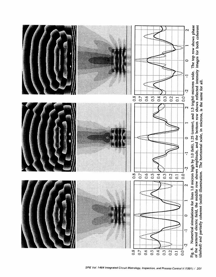
6.2 Synthetic ImagesResults of numerical simulations for lines 1.0 micron high by 1.0, 1.25, and 1.5 microns wide and lines
1.0 micron wide by 0.500, 0.695, and 0.906 microns high are presented in Figures 8 and 9. All are for thecase of TE (s-) polarized illumination. The top row of pictures in each figure shows phase of the scatteredelectric field. The middle row shows amplitude of the scattered field, all to the same gray scale. Thescattered field is isolated by subtracting the one-dimensional free-field (incident and reflected) solutionused for boundary and initial conditions from the total calculated field at each node in the model.Clearly, discontinuities in phase occur at the nulls or lows in the lobe pattern of the scattered field. These
SPIE Vol 1464 Integrated Circuit Metrology, Inspection, and Process Control V (1991) / 193

field plots are for coherent illumination, i.e., a single plane wave, at normal incidence in the picturesshown. The bottom row shows synthetic partially coherent images obtained by superposing intensityimages for 3 plane waves incident at O.O and
It is interesting to note the correlation between standing waves within the feature and the lobepattern of the scattered light. This suggests that the image for coherent illumination will be intimatelyrelated to details of the electromagnetic resonance patterns within the line. Also, since much of theinteresting phase information is at fairly shallow angles, a relatively high NA objective is necessary tosee it. However, most of this information is probably unavailable due to low side lobe intensity. Theprincipal phase information is contained in the noncylindrical wavefronts at relatively low NA.
The bottom row of pictures shows scans over each line's synthetic image assuming partially coherentillumination (3 plane waves). The coherent image (1 plane wave) is overlayed for comparison andillustrates the smoothing effect of partial coherence. The addition of more plane waves to the partiallycoherent illumination provides additional smoothing outside the micron window but has negligibleeffect within. Although there is a fairly dramatic change in the scatter pattern as the line width orheight changes, there is a relatively smooth transition between the partially coherent images. Note thatthe best indicator of line width in the partial coherence image is distance between the two primaryminima.
The synthetic scans are made by imaging the upgoing scattered and reflected (i.e., total minusincident) fields on a line across the model one element (0.0167 microns) above the feature. Maxima andminima in the coherent image scans correlate one-to-one with maxima and minima seen in the scatteredfield across the top of the feature. Closer examination of the field just above the line shows that moresubtle details in the image correlate as well, and relate to the line's interior resonance pattern. Observethat although the best measure of line width in the images is distance between the two primary minima,these correspond to field minima above the feature located approximately I /5 of the line's width fromeach edge.
6.3 Periodic versus Isolated LinesAll of our attention in this paper has been on "isolated" thick lines. Despite this bias, periodic
arrays of lines are important in CD metrology and deserve similar attention. To partially address theissue here we examine the relation between isolated and periodic line images as a function of pitch. Thisis especially relevant in the context of modeling since periodicity provides the mathematicalunderpinnings for many traditional algorithms, the waveguide model in particular, e.g., [1].
To this end we consider a periodic array of 1.Oxl.O micron lines separated by 2.0, 4.0 and 8.0 micronspaces (3, 5, and 9 micron pitches). Coherent images and scatter patterns are shown in Fig. 10. Thepictures depict the scattered field from each line out to the periodic side boundary and start with theisolated line as reference field on top. Coherent images of the object plane (line) just above the feature aredrawn over their period in the plot at the bottom of the figure. The periodic images show fair correlationwith the isolated image at 5.0 micron pitch and good correlation at 9.0 micron pitch. Similarly, thescattered field patterns are recognizable for the 5.0 micron pitch and reasonably close at 9.0 micron pitch.
Observe that the scatter patterns within and near the line cross-section show much better correlationthan the scattered field farther away. This observation suggests that better image correlation fromperiodic lines may be obtained by calculating the image from the field just outside the line and above thesilicon interface instead of from the distorted field on the object plane. This can be done by using theKirchhoff integral representation to extrapolate the electric field through free space onto an object plane,to which the imaging algorithm is applied.
7. CONCLUSIONS
These metrology simulations provide ample justification for the use of discrete numerical techniques.The results described are insightful and could not be obtained in a practical experimental fashion. Theyalso suggest the utility of numerical models for exploring other IC optical issues, particularly in overlay.Modern workstations make this type of simulation a viable addition to the IC engineer's stock ofanalysis/research tools, and may ultimately be useful in a production environment.
194 / SPIE Vol. 1464 Integrated Circuit Metrology, Inspection, and Process Control V (1991)

The comparison section has shown that reasonable to good correlation can be obtained betweenexperiments and simulations, but that discrepancies exist, some subtle and some not so subtle. The fact thatthe parameter variations considered did affect all salient features of the image implies that discrepanciesare caused by uncertainties in characterizing either the model or the imaging optics, or the scalar transferfunction assumed for the synthetic images. Once the system is adequately characterized, this workcertainly suggests that image behavior is predictable by simulation.
There still remain some questions about "completeness" of the finite element modeling, particularlyconcerning 2-D approximations of 3-D phenomena. It is also clear that partially coherent imaging warrantsfurther attention, specifically: the number of plane waves necessary and its dependence on factors likeaberrations; and cheaper alternatives to incoherent superpositions of plane wave calculations, e.g., directcalculation of the coherence function.
In terms of using simulation to calibrate a line width standard, model and microscope uncertaintiesclearly need careful attention. Accurate calibration does not appear possible without good measures ofmicroscope aberration, misalignment, and illumination nonuniformity. This is not to say that themicroscope should be perfect, only that its quantitative behavior needs to be known. Conversely,simulations provide a means to rate the imaging tool's aberrations as well as establish absolute accuracy ofboth width and shape measurements.
Extensive numerical experiments like those above, but for general substrates, are necessary before wecan make more comprehensive statements about optical metrology in the submicron realm. Modelingresearch, in conjunction with more formal inversion techniques, needs to be continued. The softwarereported here, in concert with modern workstations, will soon make such modeling accessible to engineers inthe IC industry on a routine basis.
8. ACKNOWLEDGMENTS
For their contributions to this work we would like to thank David Vaughan (Weidlinger—finiteelement code), Mecky Puiu (VLSI—ellipsometry), Dawn Cramer (SEMATECH—SEM), and Karim Tadros(UC Berkeley/VLSI—polarization). Also thanks to Michael Yeung (UC Berkeley) for a useful comment ondefocus. Support for the first two authors (G.L.W. and J.M., Jr.) was provided under a code developmentcontract with SEMATECH and several National Science Foundation Small Business Innovation Researchgrants.
9. REFERENCES
1. D. Nyyssonen, "Theory of optical edge detection and imaging of thick layers," I. Opt. Soc. Am.,72(10), pp. 1425-1436, 1982.
2. C. P. Kirk and D. Nyyssonen, "Modeling the Optical Microscope Images of Thick Layers for thePurpose of Linewidth Measurement," SPIE Vol. 538, pp. 179-187, 1985.
3. C. Yuan and A. J. Strojwas, "Modeling of Optical Alignment and Metrology Schemes Used inIntegrated Circuit Manufacturing," SPIE Vol 1264, pp. 203-218, 1990.
4. C. L. Wojcik, D. K. Vaughan, and L. K. Gaibraith, "Calculation of Light Scatter from Structures onSilicon Surfaces," SPIE Vol. 774, pp. 21-31, 1987.
5. R. Monteverde and D. Nyyssonen, "A New Line Width Standard for Reflected Light Inspection,"SPIE v:ol. 921, pp. 395-405, 1988.
6. D. Nyyssonen, "Narrow-Angle Laser Scanning Microscope System for Linewidth Measurements onWafers," National Institute of Standards and Technology Report NISTIR 88-3808, 1989.
7. M. Born and E. Wolf, Principles of Optics, Pergamon Press, New York, 1959.8. K. S. Yee, "Numerical Solution of Initial Boundary Value Problems Involving Maxwell's Equations in
Isotropic Media," IEEE Trans. Antennas Prop., Vol. AP-14, pp. 302-307, 1966.9. 0. C. Zienkiewicz, The Finite Element Method, 3r Edition, McGraw-Hill Book Co. Limited, 1977.
10. C. L. Wojcik and J. Mould, Jr., "A Mathematical Theory of Light Diffraction by Dielectric Wedges,"Conference Proceedings, 5th Annual Review of Progress in Applied Computational Electromagnetics, NavalPostgraduate School, Monterey, CA, pp. 819-826, 1989.
11. C. P. Kirk, "A Study of the Instrumental Errors in Linewidth and Registration Measurements Madewith an Optical Microscope," SPIE Vol. 775, 1987.
SPIE Vol. 1464 Integrated Circuit Metrology, Inspection, and Process Control V (1991) / 195

0.001 2 3 4 —4 -3Distance from centerline (microns)
196 / SPIE Vol. 1464 Integrated Circuit Metrology, Inspection, and Process Control V (1991)
a . Three micron line image vs. polarization0.70
b . One micron line image vs. polarization
C)
0.60
0.50
0.40
0.30
0.20
0.10
0.00-4
0.70
0.60
0.50
0.40
0.30
0.20
0.10
-3 -2 -1 0
Fig. 1. Images of the nominal three and one micron lines forTheoretically, random should be average of TE and TM polarizations.the paper are done assuming TE polarization.
three illumination polarizations.All calculations and comparisons in
S
3.3p.(226 Elements)
____ ___________ 12t(720 Elements)
Fig. 2. A blowup of the finite element grid centered around the line cross-section, showing the level ofdiscretization used. The line is 1.0 micron high and 1.0 micron wide at mid-height. The model extends 6.0microns to the left and right of center and 3.3 microns above the bottom, continuing the same discretization.

Fig. 3. Scanning electron microscope images of the VLSI Standards thick line die showing, from top tobottom, the nominal one micron line, the nominal three micron line, and the nominal fourmicron pitch. Top-down views used for line width measurement are shown on the left. Off-axis views for determination ofcross-section shape are on the right. Focused ion beam milling is used to reveal thecross-section.
SPIE Vol. 1464 Integrated Circuit Metrology, Inspection. and Process Control V (1991) / 197

0.20
0.10
0.00-4
0.20
0.10
0.00-4
0.70
0.60
0.50
0.40
0.30
0.20
0.10
0.002 3 4 -4
0.70
0.60
0.50
0.40
0.30
0.20
0.10
0.00-4 -3
0.70
0.60
0.50
0.40
0.30
0.20
0.10
0.00-4
Distance from centerline (microns)
Fig. 4. Comparisons of the microscope images (solid) and the synthetic images (dashed) for the nominalthree micron line. Plots show effect of width, defocus, and sideslope; see text for description.
198 / SPIE Vol. 1464 Integrated Circuit Metrology, Inspection, and Process Control V (1991)
0.70
0.60
0.50
0.40
0.30
a . Data vs. 3.31J. model b . 3.3 model vs. 3.4i model
&rLt1t
.: :
.j"I•:'.
%%s&
, [':_ .:'\
1. ..\
I!'::I
' I:1 I%...,:7
. : ::
.:::
" ,:•••1::: (:: ': •
:
-3 -2 -1 0
C . Data vs. 3.3J1 model, -.75L defocus0.70
0.60
0.50
0.40
0.30
-3 -2 -1 0 1 2 3
d . Data vs. 3.4j.i model, -.9i defocus
'.1
(r
-3 -2 -1 0 1 2 3 4 -2 -1 0 234f. Data VS. sloped model -.75i defocus
-3 -2 -1 0 1 2 3 4

0.70
0.60
0.50
0.40
0.30
0.20
0.10
0.00-4
0.70
0.60
0.50
0.40
0.30
0.20
0.10
0.00 —-4 -3
0.70
0.60
0.50
0.40
0.30
0.20
0.10
0.00 --4
-3 -2 -1 0 1234
234Distance from centerline (microns)
Fig. 5. Comparisons of the microscope images (solid) and the synthetic images (dashed) for the nominalone micron line. Plots show effect of width, defocus, and sideslope; see text fordescription.
SPIE Vol. 1464 Integrated Circuit Metrology, Inspection, and Process Control V (1991) / 199
a . Data vs. 1.3t model b . 1.3ji. model vs. 1.41i model0.70
0.60
0.50
0.40
0.30
0.20
0.10
. .4 . .......... ...
4 L: :fj .:. ,;
:;i::71
'
\ I,
-3 -2 -1 0 1 2 3 4
C. Data vs. 1.3ji. model, -.9Ji defocus
0.00-4
4-I
-4-I
Cl)
4-I
4
.
0.70
0.60
0.50
0.40
0.30
0.20
0.10
-3 -2 -1 0 1 2 3d. Data vs. 1.4ji model, -.9J.L defocus
4.wfJ4LMMV— 0.00-2 -1 0 1 2 3 4 -4
e . Data vs. sloped model f. Data vs. sloped model, -.9i defocus0.70
0.60
0.50
0.40
0.30
0.20
0.10
0.00-4 -3 -2
J%l
-3 -2 -1 0 1 2 3 4 -1 0 1

Distance from centerline (microns)
Distance from centerline (microns)Fig 7. Numerical experiment used to find the influence of evanescent waves on the image. The spatialspectrum is calculated on object lines 0.0167, 1 .0, and 2.0 microns above the feature, extrapolated back to theclosest line, and all three imaged. Since the images do not differ near the line, evanescent waves appearinsignificant. Observed differences are due to the 2.0 micron object line missing near-horizontal lobes shownin scattering pictures above the images.
200 / SPIE Vol. 1464 Integrated Circuit Metrology, Inspection, and Process Control V (1991)
(1)
a. Data vs. 3.3p model, -1.5? sph. aber. b. Data vs. one Ii. sloped model, 4.5k sph. aber.0.8
0.7
0.6
0.5
0.4
020.2
0.1
0.0-4
It;..L
:
JjL4-4 -3 -2 -1 -3 -2 -1 0
Fig. 6 illustration of the effect of spherical aberration on the synthetic images (dashed) plotted againstthe microscope images (solid). Lines are the 3.3 micron rectangular model (left) and and the one micronsloped model (right).
1234
a. O.5JI. wide, 1.Oji. high line0.60
0.50
0.40
0.30
0.20
0.10
0.00-6
b. 2.OJI. wide, 1.Oji. high line
... —.O.0167ji • .1 . L I.--..1.OJ.L
... --2.Oi •. .. '
0.60
0.50
0.40
0.30
0.20
0.10
0.00 --6MIck/JrwM
-4 -2 0 2 4 6 -4 -2 0 2 4 6
.. t .
:'-
0 1
2
Fig.
8.
Num
eric
al s
imul
atio
ns fo
r lin
es 1
.0 m
icro
n hi
gh b
y 1 .0
(le
ft),
I .2
5 (c
ente
r),
and
I 5 (r
ight
) m
icro
ns w
ide.
The
top
row
sho
ws p
hase
of
the
scat
tere
d el
ectr
ic f
ield
, the
mid
dle
row
sho
ws
ampl
itude
, an
d th
e bo
ttom
row
sho
ws
refl
ecte
d in
tens
ity i
mag
es f
or b
oth
cohe
rent
(d
ashe
d) a
nd p
artia
lly c
oher
ent (
solid
) illu
min
atio
n.
The
hor
izon
tal s
cale
, in
mic
rons
, is
the
sam
e fo
r al
l.
0.8
0.7
0.6
0.5
0.4
0.3
0.2
0.1
0.0
0.8
0.7
0.6
0.5
0.4
0.3
0.2
0.1
0.0
-2
—i

0.8
0.7
0.6
0.5
0.4
0.3
0.2
0.1
0.0
0.8
0.7
0.6
0.5
0.4
0.3
0.2
0.1
0.0
0.8
0.7
0.6
0.5
0.4
0.3
0.2
0.1
0.0
N
(I) 0
\J"\
Jk
"I
t\
.___
_ A
..s.
-2
-1
0 1
2.
-2
-1
0 1
2 -2
-1
0
1 2
Fig.
9.
Num
eric
al s
imul
atio
ns fo
r lin
es I
.0 m
icro
n w
ide
by 0
.5 (
left
), 0
.695
(ce
nter
), a
nd 0
.906
(ri
ght)
mic
rons
hig
h.
The
top
row
sho
ws
phas
e of
the
sca
ttere
d el
ectr
ic f
ield
, th
e m
iddl
e ro
w s
how
s am
plitu
de,
and
the
botto
m r
ow s
how
s re
flec
ted
inte
nsity
im
ages
for
bot
h co
here
nt (
dash
ed)
and
part
ially
coh
eren
t (so
lid) i
llum
inat
ion.
The
hor
izon
tal s
cale
, in
mic
rons
, is
the
sam
e fo
r al
l.

I
-6 -5 -4 -3 -2 -1 0 1 2 3 4 5 6Distance from centerline (microns)
Fig. 10. Coherent scattering patterns and images for isolated and periodic 1.Oxl.Omicron lines. Line pitchesare oo, 9.0, 5.0, and 3.0 microns respectively, starting from the top. Horizontal scale is in microns.
SPIE Vol. 1464 Integrated Circuit Metrology, Inspection, and Process Control V (1991) / 203
- - 3.0 ipitch•.--5.0ipitch. 90pitth— Isolated
I,!A1LA'I J0•
!':.E!E!.. .11 7"E..II .I'V I.III .III: .III• .Ii!1:
}:\qi/: : 't
'III .11
\4/: :________