nuc710adn 16/32-bit arm microcontroller product data sheet
TRANSCRIPT

NUC710ADN
32-BIT ARM7TDMI-BASED MCU
NUC710ADN 16/32-bit ARM microcontroller
Product Data Sheet

NUC710ADN
Publication Release Date: November23, 2013 - I - Revision A10
Table of Contents-
1. GENERAL DESCRIPTION .......................................................................................................... 1 2. FEATURES .................................................................................................................................. 2 3. PIN DIAGRAM ............................................................................................................................. 8 4. PIN ASSIGNMENTS .................................................................................................................... 9 5. PIN DESCRIPTIONS ................................................................................................................. 15 6. FUNCTIONAL DESCRIPTION .................................................................................................. 28
6.1 ARM7TDMI CPU CORE ................................................................................................ 28 6.2 System Manager ........................................................................................................... 29
6.2.1 Overview ...................................................................................................................... 29 6.2.2 System Memory Map ................................................................................................... 29 6.2.3 Address Bus Generation .............................................................................................. 32 6.2.4 Data Bus Connection with External Memory ................................................................ 32 6.2.5 Bus Arbitration ............................................................................................................. 41 6.2.6 Power management ..................................................................................................... 42 6.2.7 Power-On Setting ......................................................................................................... 44 6.2.8 System Manager Control Registers Map ..................................................................... 45
6.3 External Bus Interface ................................................................................................... 58 6.3.1 EBI Overview ............................................................................................................... 58 6.3.2 SDRAM Controller ........................................................................................................ 58 6.3.3 EBI Control Registers Map ........................................................................................... 62
6.4 Cache Controller ............................................................................................................ 80 6.4.1 On-Chip RAM ............................................................................................................... 80 6.4.2 Non-Cacheable Area ................................................................................................... 80 6.4.3 Instruction Cache ......................................................................................................... 81 6.4.4 Data Cache .................................................................................................................. 83 6.4.5 Write Buffer .................................................................................................................. 85 6.4.6 Cache Control Registers Map ...................................................................................... 85
6.5 Ethernet MAC Controller ............................................................................................... 91 6.5.1 EMC Functional Description......................................................................................... 91 6.5.2 EMC Register Mapping .............................................................................................. 101
6.6 GDMA Controller ......................................................................................................... 150 6.6.1 GDMA Functional Description .................................................................................... 150 6.6.2 GDMA Register Map .................................................................................................. 151
6.7 USB Host Controller .................................................................................................... 159 6.7.1 USB Host Functional Description ............................................................................... 159 6.7.2 USB Host Controller Registers Map ........................................................................... 160 6.7.3 HCCA ......................................................................................................................... 181 6.7.4 Endpoint Descriptor ................................................................................................... 181 6.7.5 Transfer Descriptor .................................................................................................... 181
6.8 USB Device Controller ................................................................................................. 181
NUC710ADN
Publication Release Date: November235, 2013 - II - Revision A10
6.8.1 USB Endpoints ........................................................................................................... 182 6.8.2 Standard device request ............................................................................................ 182 6.8.3 USB Device Register Description .............................................................................. 182
6.9 SD Host Controller ....................................................................................................... 218 6.9.1 Functional Description ............................................................................................... 218 6.9.2 Register Mapping ....................................................................................................... 220 6.9.3 SD Register Description ............................................................................................. 221
6.10 LCD Controller ............................................................................................................. 235 6.10.1 Main Features ............................................................................................................ 235 6.10.2 LCD Register MAP ..................................................................................................... 236 6.10.3 LCD Special Register Description .............................................................................. 238
6.11 Audio Controller ........................................................................................................... 289 6.11.1 IIS Interface ................................................................................................................ 289 6.11.2 AC97 Interface ........................................................................................................... 290 6.11.3 Audio Controller Register Map ................................................................................... 293
6.12 Universal Asynchronous Receiver/Transmitter Controller ........................................... 311 6.12.1 UART0 ....................................................................................................................... 313 6.12.2 UART1 ....................................................................................................................... 313 6.12.3 UART2 ....................................................................................................................... 315 6.12.4 UART3 ....................................................................................................................... 317 6.12.5 General UART Controller ........................................................................................... 318 6.12.6 High speed UART Controller ...................................................................................... 331
6.13 Timer/Watchdog Controller ......................................................................................... 345 6.13.1 General Timer Controller............................................................................................ 345 6.13.2 Watchdog Timer ........................................................................................................ 345 6.13.3 Timer Control Registers Map ..................................................................................... 345
6.14 Advanced Interrupt Controller ...................................................................................... 353 6.14.1 Interrupt Sources ....................................................................................................... 354 6.14.2 AIC Registers Map ..................................................................................................... 357
6.15 General-Purpose Input/Output .................................................................................... 369 6.15.1 GPIO Control Registers Map ..................................................................................... 372 6.15.2 GPIO Register Description ......................................................................................... 373
6.16 Real Time Clock .......................................................................................................... 404 6.16.1 RTC Register Map ..................................................................................................... 405 6.16.2 RTC Application Note................................................................................................. 417
6.17 Smart Card Host Interface ........................................................................................... 418 6.17.1 Register Mapping ....................................................................................................... 418 6.17.2 Register Description ................................................................................................... 420 6.17.3 Functional description ................................................................................................ 445
6.18 I2C Interface ................................................................................................................. 448 6.18.1 I2C Protocol ................................................................................................................ 449 6.18.2 I2C Serial Interface Control Registers Map ................................................................ 452

NUC710ADN
Publication Release Date: November23, 2013 - III - Revision A10
6.19 Universal Serial Interface ............................................................................................ 458 6.19.1 USI Timing Diagram ................................................................................................... 458 6.19.2 USI Registers Map ..................................................................................................... 459
6.20 PWM ............................................................................................................................ 466 6.20.1 PWM double buffering and automatic reload ............................................................. 466 6.20.2 Modulate Duty Ratio ................................................................................................... 467 6.20.3 Dead Zone Generator ................................................................................................ 467 6.20.4 PWM Timer Start procedure ...................................................................................... 468 6.20.5 PWM Timer Stop procedure ...................................................................................... 468 6.20.6 PWM Register Map .................................................................................................... 469
6.21 Keypad Interface.......................................................................................................... 476 6.21.1 Keypad Interface Register Map .................................................................................. 477 6.21.2 Register Description ................................................................................................... 478
6.22 PS2 Host Interface Controller ...................................................................................... 485 6.22.1 PS2 Host Controller Interface Register Map .............................................................. 486 6.22.2 Register Description ................................................................................................... 486
7. ELECTRICAL SPECIFICATIONS ............................................................................................ 490 7.1 Absolute Maximum Ratings ......................................................................................... 490 7.2 DC Specifications ........................................................................................................ 490
7.2.1 Digital DC Characteristics .......................................................................................... 490 7.2.2 USB Transceiver DC Characteristics ......................................................................... 493
7.3 AC Specifications ........................................................................................................ 493 7.3.1 EBI/SDRAM Interface AC Characteristics .................................................................. 493 7.3.2 EBI/(ROM/SRAM/External I/O) AC Characteristics .................................................... 494 7.3.3 USB Transceiver AC Characteristics ......................................................................... 495 7.3.4 EMC RMII AC Characteristics .................................................................................... 496 7.3.5 LCD Interface AC Characteristics .............................................................................. 498 7.3.6 SD Interface AC Characteristics ................................................................................ 499 7.3.7 AC97/I2S Interface AC Characteristics ...................................................................... 500 7.3.8 Smart Card Interface AC Characteristics ................................................................... 502 7.3.9 I2C Interface AC Characteristics ................................................................................ 503 7.3.10 USI Interface AC Characteristics ............................................................................... 504 7.3.11 PS2 Interface AC Characteristics .............................................................................. 505
8. ORDERING INFORMATION ................................................................................................... 506 9. PACKAGE SPECIFICATIONS ................................................................................................. 507 10. APPENDIX A: NUC710 REGISTERS MAPPING TABLE ........................................................ 508 11. REVISION HISTORY ............................................................................................................... 528

NUC710ADN
Publication Release Date: November23, 2013 - 1 - Revision A10
1. GENERAL DESCRIPTION The NUC710 is built around an outstanding CPU core, the 16/32 ARM7TDMI RISC processor, designed by Advanced RISC Machines, Ltd. It offers 4K-byte I-cache/SRAM and 4K-byte D-cache/SRAM, is a low power, general-purpose integrated circuit. Its simple, elegant, and fully static design is particularly suitable for cost sensitive and power sensitive applications. One 10/100 Mb MAC of Ethernet controller is built-in to reduce total system cost. An LCD controller is also built-in to support TFT and low cost STN LCD modules. With one USB 1.1 host controller, one USB 1.1 device controller, two smart card host controllers, four independent UARTs, one Watchdog timer, up to 71 programmable I/O ports, PS/2 keyboard controller and an advanced interrupt controller, the NUC710 is particularly suitable for point-of-sale (POS) system, access control and as a data collector. The NUC710 also provides one AC97/I²S controller, one SD host controller, one 2-Channel GDMA, two 24-bit timers with 8-bit pre-scale, The external bus interface (EBI) controller provides for SDRAM, ROM/SRAM, flash memory and I/O devices. The System Manager includes an internal 32-bit system bus arbiter and a PLL clock controller. With a wide range of serial communication and Ethernet interfaces, the NUC710 is also suitable for communication gateways as well as many other general-purpose applications.
NUC710ADN
Publication Release Date: November235, 2013 - 2 - Revision A10
2. FEATURES
Architecture Fully 16/32-bit RISC architecture Little/Big-Endian mode supported Efficient and powerful ARM7TDMI core Cost-effective JTAG-based debug solution
External Bus Interface 8/16/32-bit external bus support for ROM/SRAM, flash memory, SDRAM and external I/Os Support for SDRAM Programmable access cycle (0-7 wait cycle) Four-word depth write buffer for SDRAM write data Cost-effective memory-to-peripheral DMA interface
Instruction and Data Cache Two-way, Set-associative, 4K-byte I-cache and 4K-byte D-cache Support for LRU (Least Recently Used) Protocol Cache can be configured as internal SRAM Support Cache Lock function
Ethernet MAC Controller DMA engine with burst mode MAC Tx/Rx buffers (256 bytes Tx, 256 bytes Rx) Data alignment logic Endian translation 100/10-Mbit per second operation Full compliance with IEEE standard 802.3 RMII interface only Station Management Signaling On-Chip CAM (up to 16 destination addresses) Full-duplex mode with PAUSE feature Long/short packet modes PAD generation

NUC710ADN
Publication Release Date: November23, 2013 - 3 - Revision A10
LCD Controller (LCDC)
(1) STN LCD Display Supports 4-bit single scan Monochrome STN LCD panel, 8-bit single scan Monochrome STN LCD
panel, 8-bit single scan Color STN LCD panel Up to 16 gray levels display for Monochrome STN LCD panel Up to 4096(12bpp) colors display for Color STN LCD panel Virtual coloring method: Frame Rate Control (16-level) Anti-flickering method: Time-based Dithering
(2) TFT LCD Display Supports Sync-type TFT LCD panel and Sync-type High-color TFT LCD panel Supports direct or palletized color display
(3) TV Encoder Supports 8-bit YCbCr data output format to connect with external TV Encoder
(4) LCD Preprocessing Supports RGB Raw-data or YUV422 packet format Programmable parameters for different image sizes Two built-in FIFOs, FIFO 1 is for Video images and FIFO 2 is for OSD images. Each FIFO is 16
words deep
(5) LCD Post processing Support for one OSD (On-Screen-Display) overlay Supports various OSD functions Programmable parameters for different display panels
(6) Others Color-look up table size 256x32 bit for TFT used when displaying 1bpp, 2bpp, 4bpp, 8bpp image Dedicated DMA for block transfer mode
DMA Controller 2-channel General DMA for memory-to-memory data transfers without CPU intervention Initialed by a software or external DMA request Increments or decrements a source or destination address in 8-bit, 16-bit or 32-bit data transfers 4-data burst mode
UART Four UART (serial I/O) blocks with interrupt-based operation Support for 5-bit, 6-bit, 7-bit or 8-bit serial data transmission Programmable baud rates 1, ½ or 2 stop bits
NUC710ADN
Publication Release Date: November235, 2013 - 4 - Revision A10
Odd or even parity Break generation and detection Parity, overrun and framing error detection X16 clock mode UART1 supports Bluetooth, and UART2 supports IrDA1.0 SIR
Timers Two programmable 24-bit timers with 8-bit prescaler One programmable 20-bit timer with optional 8-bit prescaler Watchdog timer One-shot mode, periodical mode or toggle mode operation
Programmable I/Os 71 programmable I/O ports Pins individually configurable for input, output or I/O mode for dedicated signals I/O ports are configurable for Multiple functions
Advanced Interrupt Controller 31 interrupt sources, including 6 external interrupt sources Programmable normal or fast interrupt mode (IRQ, FIQ) Programmable as either edge-triggered or level-sensitive for 6 external interrupt sources Programmable as either low-active or high-active for 6 external interrupt sources Priority methodology is encoded to allow for interrupt daisy-chaining Automatically mask out the lower priority interrupt during interrupt nesting
USB Host Controller USB 1.1 compliant Compatible with Open HCI 1.0 specification Supports low-speed and full speed devices Built-in DMA for real time data transfer Two on-chip USB transceivers with one optionally shared with USB Device Controller
USB Device Controller USB 1.1 compliant Supports four USB endpoints including one control endpoint and 3 configurable endpoints for rich
USB functions
Two PLLs The external clock can be multiplied by on-chip PLL to provide high frequency system clock The input frequency range is 3-30MHz; 15MHz is preferred. One PLL for both CPU and USB host/device controller
NUC710ADN
Publication Release Date: November23, 2013 - 5 - Revision A10
One PLL for LCD pixel clock and audio IIS 12.288/16.934MHz clock source Programmable clock frequency
Real Time Clock (RTC) 32.768KHz operation Time counter (second, minute, hour) and calendar counter (day, month, year) Alarm register (second, minute, hour, day, month, year) 12 or 24-hour mode selectable Automatically recognizes leap years Weekday counter Frequency compensate register (FCR) Besides the FCR, all clock and alarm data are expressed in BCD Supports tick time interrupts
4-Channel PWM Four 16-bit timers with PWM Two 8-bit prescalers & Two 4-bit dividers Programmable duty control of output waveform Auto reload mode or one-shot pulse mode Dead-zone generator
I2C Master Two Channel I2C Compatible with Philips I2C standard, support master mode only Supports multi master operation Clock stretching and wait state generation Provides multi-byte transmission, up to 4 bytes can be transmitted in a single transfer Software programmable acknowledge bit Arbitration lost interrupt, with automatic transfer cancellation Start/Stop/Repeated Start/Acknowledge generation Start/Stop/Repeated Start detection Bus busy detection Supports 7 bit addressing mode Software mode I2C

NUC710ADN
Publication Release Date: November235, 2013 - 6 - Revision A10
Universal Serial Interface (USI) 1-Channel USI Support USI (Microwire/SPI) master mode Full duplex synchronous serial data transfer Variable length of transfer word up to 32 bits Provide burst mode operation, transmit/receive can be executed up to four times in one transfer MSB or LSB first data transfer Rx and Tx on both positive or negative edge of serial clock independently Two slave/device select lines Fully static synchronous design with one clock domain
2-Channel AC97/I2S Audio Codec Host Interface AHB master port and an AHB slave port are offered in the audio controller. 8-beat incrementing burst Bus lock during 8-beat incrementing burst At the middle or end of a destination address, a DMA_IRQ is automatically requested from the
CPU
Smart Card Host Interface (SCHI) ISO-7816 compliant PC/SC T=0, T=1 compliant 16-byte transmitter FIFO and 16-byte receiver FIFO FIFO threshold interrupt to optimize system performance
Programmable transmission clock frequency Versatile baud rate configuration UART-like register file structure General-purpose C4, C8 channels
SD Host Interface Directly connect to Secure Digital (SD, MMC) flash memory card. Supports DMA functions to accelerate the data transfer between the internal buffer, external
SDRAM, and flash memory cards. Two 512 byte internal buffers are embedded inside the controller. No SPI mode.
KeyPad Scan Interface Scan up to 16 rows by 8 columns with an external 4 to 16 decoder and 4 rows by 8 columns array
without auxiliary components Programmable de-bounce time

NUC710ADN
Publication Release Date: November23, 2013 - 7 - Revision A10
One or two keys scan with interrupt and three keys reset function. Wakeup CPU from IDEL/Power Down mode
PS2 Host Interface APB slave consisted of PS2 protocol. Connect IBM keyboard or bar code reader through PS2 interface. Provide hardware scan code to ASCII translation
Power management Programmable clock enables individual peripherals IDLE mode to halt ARM Core and keep peripheral working Power-Down mode to stop all clocks included external crystal oscillator. Exit IDLE by all interrupts Exit Power-Down by keypad, USB device and external interrupts
Operating Voltage Range 3.0 ~ 3.6 V for IO Buffer 1.62 ~ 1.98 V for Core Logic
Operating Temperature Range -40 ~ +85
Operating Frequency Up to 80 MHz
Package Type 176-pin LQFP

NUC710ADN
Publication Release Date: November235, 2013 - 8 - Revision A10
3. PIN DIAGRAM
85
140
50 55 60 80757065
165
160
155
150
145
175
170
VSS18KPI_ROW[0]/VCLK/GPIO[30]
KPI_COL[1]/VD[1]/GPIO[35]
TXD1/GPIO[7]
VDD33
MCKE
nBTC
S
nSCS[1]
nSCS[0]
SCL0/SFRM/TIMER0/GPIO[11]
SCL1/SCLK/KPI_ROW[3]/GPIO[13]SDA0/SSPTXD/TIMER1/GPIO[12]
D[10]/TB
US[10]
D[11]/TB
US[11]
SDA1/SSPRXD/KPI_ROW[2]/GPIO[14]
KPI_ROW[2]/VSYNC/GPIO[32]
KPI_COL[7]/VD[7]/GPIO[41]KPI_ROW[3]/HSYNC/GPIO[33]
KPI_ROW[1]/VDEN/GPIO[31]
VDD18
nECS[1]
nWAIT/TREQB
nECS[0]nOE
D[26]/VD[18]/GPIO[62]D[27]/VD[19]/GPIO[63]
D[24]/VD[16]/GPIO[60]D[25]/VD[17]/GPIO[61]
TDI
VDD33
A[10]/TBUS[26]
A[9]/TBUS[25]
A[13]/TBUS[29]A[12]/TBUS[28]
nIRQ[1]/GPIO[17]
TCK
TDO
USB0VDD
SC0_PW
R/S
D_D
AT2/V
D[13]/G
PIO[25]
SC0_R
ST/S
D_D
AT0/V
D[15]/G
PIO[27]
SC0_C
LK/S
D_C
LK/V
D[16]/G
PIO[28]
SC0_D
AT/S
D_C
MD
/VD
[17]/[GPIO
[29]VSS18
VD
D18
AC97_B
ITCLK
/I2S_B
ITCLK
/PWM
[3]/RXD
3/GPIO
[4]AC97_S
YNC/I2S
_LRCLK
/PWM
[2]/TXD
3/GPIO
[3]AC97_D
ATA
O/I2S
_DATA
O/PW
M[1]/D
SR3/G
PIO[2]
AC97_D
ATA
I/I2S_D
ATA
I/PWM
[0]/DTR
3/GPIO
[1]
nTRST
EXTA
L(15M)
VD
D33
SC0_PR
ES/S
D_D
AT1/V
D[14]/G
PIO[26]
SC1_D
AT/S
D_D
AT3/V
D[12]/G
PIO[24]
EXTA
L32 (32.768K)
RTC
VD
D18
VSS33
XTA
L32 (32.768K)
AC97_nR
ESET/I2S
_MCLK
/GPIO
[0]
nWD
OG
/GPIO
[15]
VSS33A[4]/TBUS[20]A[3]/TBUS[19]A[2]/TBUS[18]
VDD33D[28]/VD[20]/GPIO[64]
D[30]/VD[22]/GPIO[66]
A[21]
VD
D33
XTA
L(15M)
VSS33
A[18]A[17]/TREQAVDD18
A[8]/TBUS[24]A[7]/TBUS[23]A[6]/TBUS[22]A[5]/TBUS[21]
KPI_COL[3]/VD[3]/GPIO[37]
KPI_COL[0]/VD[0]/GPIO[34]
nRESET
PLL1VSS18
KPI_COL[2]/VD[2]/GPIO[36]
KPI_COL[4]/VD[4]/GPIO[38]
PLL0VSS18PLL0VDD18
TEST
A[20]A[19]
VDD33
D[31]/VD[23]/GPIO[67]
A[11]/TBUS[27]
D[29]/VD[21]/GPIO[65]
KPI_COL[6]/VD[6]/GPIO[40]KPI_COL[5]/VD[5]/GPIO[39]
PHY_R
XD
[0]/GPIO
[44]/KPI_C
OL[2]/V
D[10]
PHY_C
RSD
V/G
PIO[43]/K
PI_CO
L[1]/VD
[9]PH
Y_RXER
R/G
PIO[42]/K
PI_CO
L[0]/VD
[8]SC1_PW
R/nX
DACK/V
D[8]/G
PIO[20]
SC1_PR
ES/nX
DREQ
/VD
[9]GPIO
[21]SC1_R
ST/S
D_C
D/V
D[10]/G
PIO[22]
SC1_C
LK/S
D_PW
R/V
D[11]/G
PIO[23]
VSS33
PLL1VDD18A[1]/TBUS[17]A[0]/TBUS[16]
PHY_M
DC/G
PIO[51]/K
P_RO
W[1]/V
D[17]
PHY_TX
D[1]/G
PIO[49]/K
PI_CO
L[7]/VD
[15]
nIRQ[0]/GPIO[16]
A[16]/TACKA[15]/TBUS[31]A[14]/TBUS[30]VSS18
TMS
RXD1/GPIO[8]
VSS33RTS1/RXD2(IrDA)/PS2_DATA/GPIO[10]
CTS1/TXD2(IrDA)/PS2_CLK/GPIO[9]
nWE
PHY_TX
D[0]/G
PIO[48]/K
PI_CO
L[6]/VD
[14]PH
Y_TXEN
/GPIO
[47]/KPI_C
OL[5]/V
D[13]
PHY_R
EFCLK
/GPIO
[46]/KPI_C
OL[4]/V
D[12]
PHY_R
XD
[1]/GPIO
[45]/KPI_C
OL[3]/V
D[11]
VSS33
D[22]/V
D[14]/G
PIO[58]
D[20]/V
D[12]/G
PIO[56]
D[21]/V
D[13]/G
PIO[57]
nWBE[0]/S
DQ
M[0]
D[13]/TB
US[13]
D[19]/V
D[11]/G
PIO[55]
nWBE[3]/S
DQ
M[3]/G
PIO[69]
nWBE[1]/S
DQ
M[1]
D[23]/V
D[15]/G
PIO[59]
nIRQ
[3]/GPIO
[19]nIR
Q[2]/G
PIO[18]
D[18]/V
D[10]/G
PIO[54]
D[14]/TB
US[14]
D[15]/TB
US[15]
VSS18
VD
D18
D[17]/V
D[9]/G
PIO[53]
D[16]/V
D[8]/G
PIO[52]
VSS33
D[12]/TB
US[12]
D[3]/TB
US[3]
VD
D33
nWBE[2]/S
DQ
M[2]/G
PIO[68]
D[2]/TB
US[2]
D[0]/TB
US[0]
D[1]/TB
US[1]
MCLK
VD
D33
nECS[2]
nECS[3]
nSRAS
nSCAS
VSS33VDD33
135
TXD0/GPIO[5]
DN0DP0
RXD0/GPIO[6]
USB1VSSDN1
USB1VDDDP1
D[6]/TB
US[6]
5
10
15
20
25
30
35
40
95
90
120
110
105
100
130
125
D[4]/TB
US[4]
VSS33
D[5]/TB
US[5]
USB0VSS
D[9]/TB
US[9]
D[7]/TB
US[7]
D[8]/TB
US[8]
PHY_M
DIO
/GPIO
[50]/KPI_R
OW
[0]/VD
[16]
VD
D33
115
NUC710ADN176 -pin
LQFP
VSS33
Fig 3.1 Pin Diagram

NUC710ADN
Publication Release Date: November23, 2013 - 9 - Revision A10
4. PIN ASSIGNMENTS Table 4.1 NUC710 Pin Assignments
PIN NAME 176-PIN LQFP
Clock & Reset ( 5 pins ) EXTAL (15M) 52 XTAL (15M) 53 EXTAL32 (32.768K) 57 XTAL32 (32.768K) 56 nRESET 37 JTAG Interface ( 5 pins ) TMS 45 TDI 46 TDO 47 TCK 48 nTRST 49 External Bus Interface ( 72 pins ) A [21] 115
A [20:0] 113-110,108-106, 104-101,99-95, 93-89
D [31:16] / VD [23:8] / GPIO [67:52]
116-119,121-124, 149-156
D [15:0] 158,159,161-164, 166-170,172-176 nWBE [3:2] / SDQM [3:2] / GPIO[69:68]
146,145
nWBE [1;0] / SDQM [1:0] 144,143
nSCS [1:0] 136,135 nSRAS 137 nSCAS 138 MCKE 134 nSWE 142 MCLK 140 nWAIT/ GPIO[70] / nIRQ5
132
nBTCS 133 nECS [3] 125 nECS [2:0] 128-130 nOE 131

NUC710ADN
Publication Release Date: November235, 2013 - 10 - Revision A10
Table 4.1 NUC710 Pin Assignments (Continued)
PIN NAME 176-PIN LQFP
Ethernet Interface ( 10 pins ) PHY_MDC / GPIO [51] / KPROW[1] / VD[17]
88
PHY_MDIO / GPIO [50] / KPROW[0] / LD[16]
87
PHY_TXD [1:0] / GPIO[49:48] / KPCOL[7:6] / VD[15:14]
86,84
PHY_TXEN / GPIO [47] / KPCOL[5] / VD[13]
83
PHY_REFCLK / GPIO [46] / KPCOL[4] / VD[12]
82
PHY_RXD [1:0] / GPIO [45:44] / KPCOL[3:2] / VD[11:10]
81,79
PHY_CRSDV / GPIO [43] / KPCOL[1] / VD[9]
78
PHY_RXERR / GPIO [42] / KPCOL[0] / VD[8]
77
AC97/I2S/PWM/UART3 ( 5 pins ) AC97_nRESET / I2S_MCLK / GPIO [0] / USB_PWREN
58

NUC710ADN
Publication Release Date: November23, 2013 - 11 - Revision A10
Table 4.1 NUC710 Pin Assignments (Continued)
PIN NAME 176-PIN LQFP
AC97/I2S/PWM/UART3 ( 5 pins ) AC97_DATAI / I2S_DATAI / PWM [0] / DTR3 / GPIO [1]
59
AC97_DATAO / I2S_DATAO / PWM [1] / DSR3 / GPIO [2]
60
AC97_SYNC / I2S_LRCLK / PWM [2] / TXD3 / GPIO [3]
61
AC97_BITCLK / I2S_BITCLK / PWM [3] / RXD3 GPIO [4]
62
USB Interface ( 4 pins ) DP0 7 DN 0 6 DP1 2 DN1 3 Miscellaneous ( 7 pins ) nIRQ [3:2] / GPIO [19:18]
148,147
nIRQ [1] / GPIO [17] / USB_OVRCUR
44
nIRQ [0] / GPIO [16]
43
nWDOG / GPIO [15] / USB_PWREN
50
RTCVDD18 55
NUC710ADN
Publication Release Date: November235, 2013 - 12 - Revision A10
Table 4.1 NUC710 Pin Assignments (Continued)
NAME 176-PIN LQFP
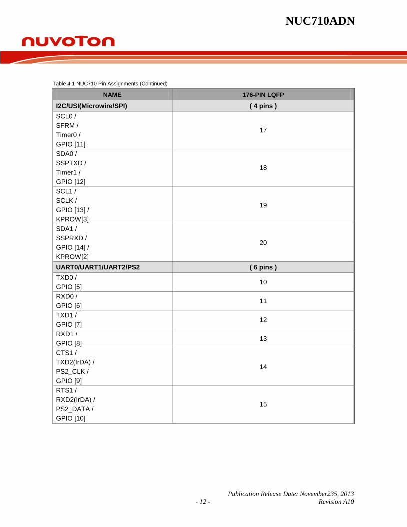
I2C/USI(Microwire/SPI) ( 4 pins ) SCL0 / SFRM / Timer0 / GPIO [11]
17
SDA0 / SSPTXD / Timer1 / GPIO [12]
18
SCL1 / SCLK / GPIO [13] / KPROW[3]
19
SDA1 / SSPRXD / GPIO [14] / KPROW[2]
20
UART0/UART1/UART2/PS2 ( 6 pins ) TXD0 / GPIO [5]
10
RXD0 / GPIO [6]
11
TXD1 / GPIO [7]
12
RXD1 / GPIO [8]
13
CTS1 / TXD2(IrDA) / PS2_CLK / GPIO [9]
14
RTS1 / RXD2(IrDA) / PS2_DATA / GPIO [10]
15
NUC710ADN
Publication Release Date: November23, 2013 - 13 - Revision A10
Table 4.1 NUC710 Pin Assignments (Continued)
NAME 176-PIN LQFP
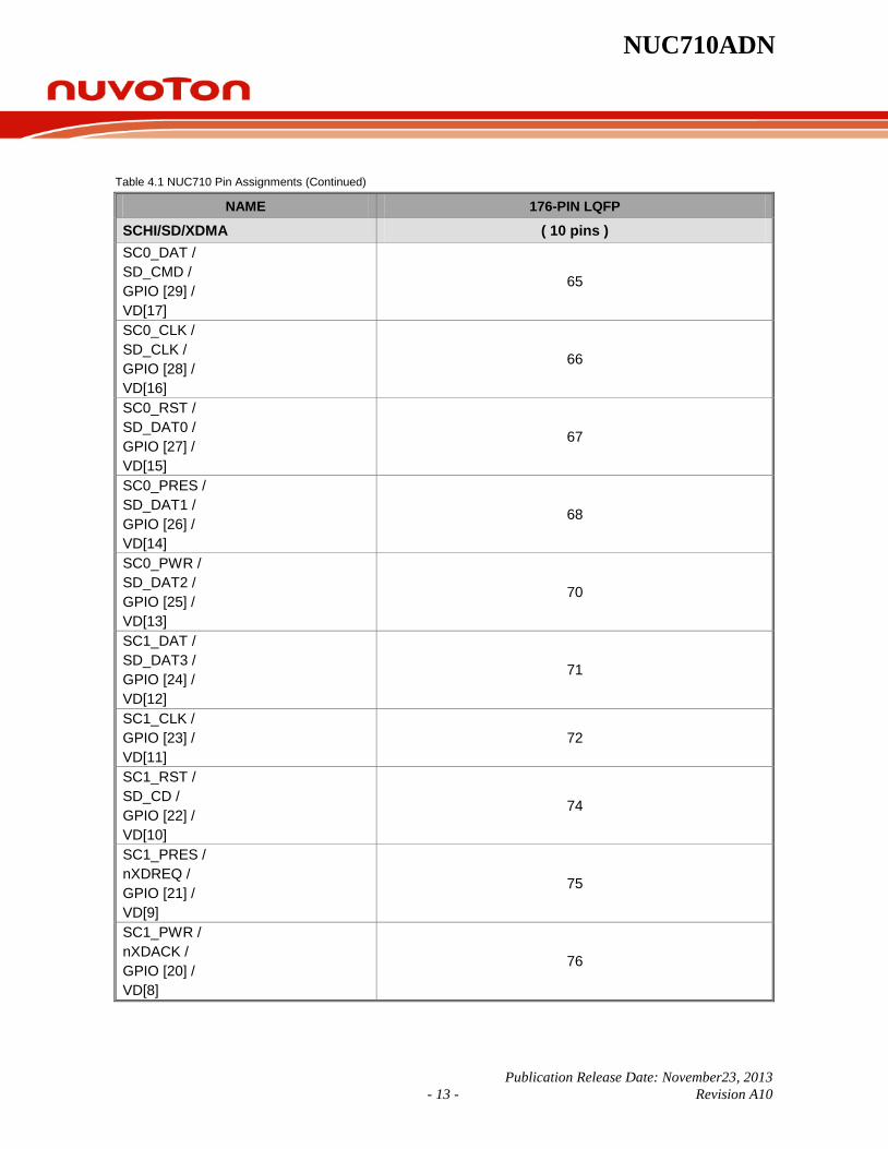
SCHI/SD/XDMA ( 10 pins ) SC0_DAT / SD_CMD / GPIO [29] / VD[17]
65
SC0_CLK / SD_CLK / GPIO [28] / VD[16]
66
SC0_RST / SD_DAT0 / GPIO [27] / VD[15]
67
SC0_PRES / SD_DAT1 / GPIO [26] / VD[14]
68
SC0_PWR / SD_DAT2 / GPIO [25] / VD[13]
70
SC1_DAT / SD_DAT3 / GPIO [24] / VD[12]
71
SC1_CLK / GPIO [23] / VD[11]
72
SC1_RST / SD_CD / GPIO [22] / VD[10]
74
SC1_PRES / nXDREQ / GPIO [21] / VD[9]
75
SC1_PWR / nXDACK / GPIO [20] / VD[8]
76

NUC710ADN
Publication Release Date: November235, 2013 - 14 - Revision A10
Table 4.1 NUC710 Pin Assignments (Continued)
NAME 176-PIN LQFP
LCDC ( 12 pins ) VD[7:0] / GPIO [41:34]/ KPCOL[7:0]
27-34
HSYNC / GPIO [33]/ KPROW[3]
26
VSYNC / GPIO [32]/ KPROW[2]
25
VDEN / GPIO [31]/ KPROW[1]
24
VCLK / GPIO [30]/ KPROW[0]
23
Power/Ground ( 36 pins ) VDD18 21,63,109,160 VSS18 22,38,64,105,157
VDD33 9,35,54,69,85,100, 120,127,139,165
VSS33 16,36,51,73,80,94, 114,126,141,171
USBVDD 1,8 USBVSS 4,5 PLLVDD18 39,42 PLLVSS18 40,41
NUC710ADN
Publication Release Date: November23, 2013 - 15 - Revision A10
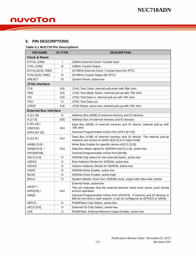
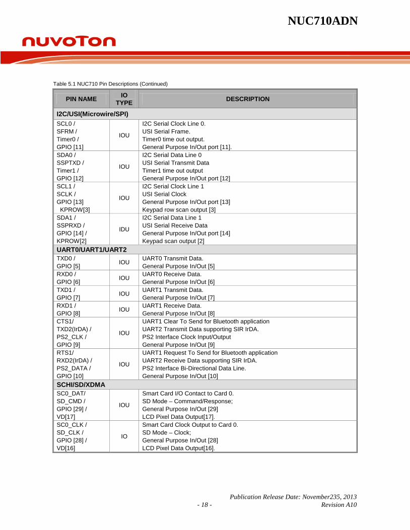
5. PIN DESCRIPTIONS Table 5.1 NUC710 Pin Descriptions
PIN NAME IO TYPE DESCRIPTION Clock & Reset EXTAL (15M) I 15MHz External Clock / Crystal Input XTAL (15M) O 15MHz Crystal Output EXTAL32(32.768K) I 32768Hz External Clock / Crystal Input (for RTC) XTAL32(32.768K) O 32768Hz Crystal Output (for RTC) nRESET IS System Reset, active-low JTAG Interface TCK IDS JTAG Test Clock, internal pull-down with 58K ohm TMS IUS JTAG Test Mode Select, internal pull-up with 70K ohm TDI IUS JTAG Test Data in, internal pull-up with 70K ohm TDO O JTAG Test Data out nTRST IUS JTAG Reset, active-low, internal pull-up with 70K ohm External Bus Interface A [21:18] O Address Bus (MSB) of external memory and IO devices. A [17:0] IOS Address Bus of external memory and IO devices. D [31:16] / VD[23:8] / GPIO [67:52]
IOU Data Bus (MSB) of external memory and IO device, internal pull-up with 70K ohm. General Programmable In/Out Port GPIO [67:52].
D [15:0] / IOU Data Bus (LSB) of external memory and IO device. The internal pull-up resistors are turned on when D[15:0] is in input mode.
nWBE [3:0] / SDQM [3:0] / GPIO[69:68]
IOU Write Byte Enable for specific device (nECS [3:0]). Data Bus Mask signal for SDRAM (nSCS [1:0]), active-low. General Programmable In/Out Port [69:68]
nSCS [1:0] O SDRAM chip select for two external banks, active-low. nSRAS O Row Address Strobe for SDRAM, active-low. nSCAS O Column Address Strobe for SDRAM, active-low. nSWE O SDRAM Write Enable, active-low MCKE O SDRAM Clock Enable, active-high MCLK O System Master Clock Out, SDRAM clock, output with slew-rate control
nWAIT / GPIO[70] / nIRQ5
IOU
External Wait, active-low. This pin indicates that the external devices need more active cycle during access operation. General Programmable In/Out Port GPIO[70]. If memory and IO devices in EBI do not need a wait request, it can be configured as GPIO[7] or nIRQ5
nBTCS O ROM/Flash Chip Select, active-low. nECS [3:0] O External I/O Chip Select, active-low. nOE O ROM/Flash, External Memory Output Enable, active-low.

NUC710ADN
Publication Release Date: November235, 2013 - 16 - Revision A10
Table 5.1 NUC710 Pin Descriptions (Continued)
PIN NAME IO TYPE DESCRIPTION
Ethernet Interface
PHY_MDC / GPIO [51] / KPROW[1] / VD[17]
IOU
RMII Management Data Clock for Ethernet. It is the reference clock of MDIO. Each MDIO data will be latched at the positive edge of MDC clock. General Programmable In/Out Port [51] Keypad ROW[1] scan output. LCD Pixel Data Output[17].
PHY_MDIO / GPIO [50] / KPROW[0] / VD[16]
IO
RMII Management Data I/O for Ethernet. It is used to transfer RMII control and status information between PHY and MAC. General Programmable In/Out Port [51] Keypad ROW[0] scan output. LCD Pixel Data Output[16].
PHY_TXD [1:0] / GPIO [49:48] / KPCOL[7:6] / VD[15]
IOU
2-bit Transmit Data bus for Ethernet. General programmable In/Out Port [49:48] Keypad Column input [7:6], active low LCD Pixel Data Output[15].
PHY_TXEN / GPIO [47] / KPCOL[5] / VD[14:13]
IOU
PHY_TXEN shall be asserted synchronously with the first 2-bits of the preamble and shall remain asserted while all di-bits to be transmitted present. Of course, it is synchronized with PHY_REFCLK. General Programmable In/Out Port [47] Keypad column input [5], active low LCD Pixel Data Output[14:13].
PHY_REFCLK / GPIO [46] / KPCOL[4] / VD[12]
IOS
Reference Clock. The clock shall be 50MHz +/- 50 ppm with minimum 35% duty cycle at high or low state. General Programmable In/Out port [46] Keypad column input [4], active low LCD Pixel Data Output[12].
PHY_RXD [1:0] / GPIO [45:44] / KPCOL[3:2] / VD[11:10]
IOS
2-bit Receive Data bus for Ethernet. General Programmable In/Out Port [45:44] Keypad column input [3:2], active low LCD Pixel Data Output[11:10].
PHY_CRSDV / GPIO [43] / KPCOL[1] / VD[9]
IOS
Carrier Sense / Receive Data Valid for Ethernet. The PHY_CRSDV shall be asserted by PHY when the receive medium is non-idle. Loss of carrier shall result in the de-assertion of PHY_CRSDV synchronous to the cycle of PHY_REFCLK, and only on 2-bit receive data boundaries. General Programmable In/Out port [43] Keypad column input [1], active low LCD Pixel Data Output[9].
PHY_RXERR / GPIO [42] / KPCOL[0] / VD[8]
IOS
Receive Data Error for Ethernet indicates a data error detected by PHY. The assertion should last longer than the period of PHY_REFCLK. When PHY_RXERR is asserted, the MAC will report a CRC error. General programmable In/Out port [42] Keypad column input [0], active low LCD Pixel Data Output[8].
Table 5.1 NUC710 Pin Descriptions (Continued)
PIN NAME IO TYPE DESCRIPTION
AC97/I2S/PWM/UART3
NUC710ADN
Publication Release Date: November23, 2013 - 17 - Revision A10
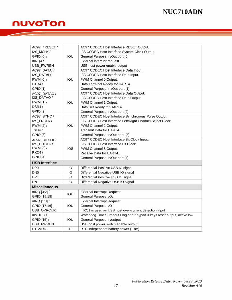
AC97_nRESET / I2S_MCLK / GPIO [0] / nIRQ4 / USB_PWREN
IOU
AC97 CODEC Host Interface RESET Output. I2S CODEC Host Interface System Clock Output. General Purpose In/Out port [0] External interrupt request. USB host power enable output
AC97_DATAI / I2S_DATAI / PWM [0] / DTR4 / GPIO [1]
IOU
AC97 CODEC Host Interface Data Input. I2S CODEC Host Interface Data Input. PWM Channel 0 Output. Data Terminal Ready for UART4. General Purpose In /Out port [1]
AC97_DATAO / I2S_DATAO / PWM [1] / DSR4 / GPIO [2]
IOU
AC97 CODEC Host Interface Data Output. I2S CODEC Host Interface Data Output. PWM Channel 1 Output. Data Set Ready for UART4. General Purpose In/Out port [2]
AC97_SYNC / I2S_LRCLK / PWM [2] / TXD4 / GPIO [3]
IOU
AC97 CODEC Host Interface Synchronous Pulse Output. I2S CODEC Host Interface Left/Right Channel Select Clock. PWM Channel 2 Output. Transmit Data for UART4. General Purpose In/Out port [3]
AC97_BITCLK / I2S_BITCLK / PWM [3] / RXD4 / GPIO [4]
IOS
AC97 CODEC Host Interface Bit Clock Input. I2S CODEC Host Interface Bit Clock. PWM Channel 3 Output. Receive Data for UART4. General Purpose In/Out port [4].
USB Interface DP0 IO Differential Positive USB IO signal DN0 IO Differential Negative USB IO signal DP1 IO Differential Positive USB IO signal DN1 IO Differential Negative USB IO signal Miscellaneous nIRQ [3:2] / GPIO [19:18]
IOU External Interrupt Request General Purpose I/O.
nIRQ [1:0] / GPIO [17:16] USB_OVRCUR
IOU External Interrupt Request General Purpose I/O nIRQ1 is used as USB host over-current detection input
nWDOG / GPIO [15] / USB_PWREN
IOU Watchdog Timer Timeout Flag and Keypad 3-keys reset output, active low General Purpose In/output USB host power switch enable output
RTCVDD P RTC independent battery power (1.8V)
NUC710ADN
Publication Release Date: November235, 2013 - 18 - Revision A10
Table 5.1 NUC710 Pin Descriptions (Continued)
PIN NAME IO TYPE DESCRIPTION
I2C/USI(Microwire/SPI) SCL0 / SFRM / Timer0 / GPIO [11]
IOU
I2C Serial Clock Line 0. USI Serial Frame. Timer0 time out output. General Purpose In/Out port [11].
SDA0 / SSPTXD / Timer1 / GPIO [12]
IOU
I2C Serial Data Line 0 USI Serial Transmit Data Timer1 time out output General Purpose In/Out port [12]
SCL1 / SCLK / GPIO [13] KPROW[3]
IOU
I2C Serial Clock Line 1 USI Serial Clock General Purpose In/Out port [13] Keypad row scan output [3]
SDA1 / SSPRXD / GPIO [14] / KPROW[2]
IDU
I2C Serial Data Line 1 USI Serial Receive Data General Purpose In/Out port [14] Keypad scan output [2]
UART0/UART1/UART2 TXD0 / GPIO [5] IOU UART0 Transmit Data.
General Purpose In/Out [5] RXD0 / GPIO [6] IOU UART0 Receive Data.
General Purpose In/Out [6] TXD1 / GPIO [7] IOU UART1 Transmit Data.
General Purpose In/Out [7] RXD1 / GPIO [8] IOU UART1 Receive Data.
General Purpose In/Out [8] CTS1/ TXD2(IrDA) / PS2_CLK / GPIO [9]
IOU
UART1 Clear To Send for Bluetooth application UART2 Transmit Data supporting SIR IrDA. PS2 Interface Clock Input/Output General Purpose In/Out [9]
RTS1/ RXD2(IrDA) / PS2_DATA / GPIO [10]
IOU
UART1 Request To Send for Bluetooth application UART2 Receive Data supporting SIR IrDA. PS2 Interface Bi-Directional Data Line. General Purpose In/Out [10]
SCHI/SD/XDMA SC0_DAT/ SD_CMD / GPIO [29] / VD[17]
IOU
Smart Card I/O Contact to Card 0. SD Mode – Command/Response; General Purpose In/Out [29] LCD Pixel Data Output[17].
SC0_CLK / SD_CLK / GPIO [28] / VD[16]
IO
Smart Card Clock Output to Card 0. SD Mode – Clock; General Purpose In/Out [28] LCD Pixel Data Output[16].

NUC710ADN
Publication Release Date: November23, 2013 - 19 - Revision A10
Table 5.1 NUC710 Pin Descriptions (Continued)
PIN NAME IO TYPE DESCRIPTION
SCHI/SD/XDMA SC0_RST / SD_DAT0 / GPIO [27] / VD[15]
IO
Smart Card Reset Output to Card 0. SD Mode – Data Line Bit 0; General Purpose In/Out [27] LCD Pixel Data Output[15].
SC0_PRES / SD_DAT1 / GPIO [26] VD[14]
IO
Smart Card 0 Presence Contact Input. SD Mode – Data Line Bit 1. General Purpose In/Out [26] LCD Pixel Data Output[14].]
SC0_nPWR / SD_DAT2 / GPIO [25] / VD[13]
IO
Smart Card 0 Power FET Control Signal Output. SD Mode – Data Line Bit 2. General Purpose In/Out [25] LCD Pixel Data Output[13].
SC1_DAT / SD_DAT3 / GPIO [24] / VD[12]
IO
Smart Card I/O Contact to Card 1. SD Mode – Data Line Bit 3; General Purpose In/Out [24] LCD Pixel Data Output[12].
SC1_CLK / GPIO [23] / VD[11]
IO Smart Card Clock Output to Card 1. General Purpose In/Out [23] LCD Pixel Data Output[11].
SC1_RST / SD_CD / GPIO [22] / VD[10]
IO
Smart Card Reset Output to Card 1. SD Mode – Card Detect. General Purpose In/Out [22] LCD Pixel Data Output[10].
SC1_PRES / nXDREQ / GPIO [21] / VD[9]
IO
Smart Card 1 Presence Contact Input. External DMA Request. General Purpose In/Out [21] LCD Pixel Data Output[9].
SC1_nPWR / nXDACK / GPIO [20] / VD[8]
IO
Smart Card 1 Power FET Control Signal Output. External DMA Acknowledgement. General Purpose In/Out [20] LCD Pixel Data Output[8].
LCD Interface VD [7:0] / GPIO [41:34]/ KPCOL[7:0]
IOU LCD Pixel Data Output [7:0]. General Purpose In/Out [41:34] Keypad Column input [7:0], active low
HSYNC / GPIO [33]/ KPROW[3]
IOU Horizontal Sync General Purpose In/Out [33] Keypad ROW[3] scan output.
VSYNC / GPIO [32]/ KPROW[2]
IOU Vertical Sync General Purpose In/Out [32] Keypad ROW[2] scan output.
VDEN / GPIO [31]/ KPROW[1]
IOU Data Enable or Display Control Signal. General Purpose In/Out [31] Keypad ROW[1] scan output.

NUC710ADN
Publication Release Date: November235, 2013 - 20 - Revision A10
Table 5.1 NUC710 Pins Description (Continued)
PIN NAME IO TYPE DESCRIPTION
Power/Ground VDD18 P Core Logic power (1.8V)
VSS18 G Core Logic ground (0V)
VDD33 P IO Buffer power (3.3V)
VSS33 G IO Buffer ground (0V)
USBVDD P USB power (3.3V)
USBVSS G USB ground (0V)
PLL0_VDD18 P PLL 0 power (1.8V)
PLL0_VSS18 G PLL 0 ground (0V)
PLL1_VDD18 P PLL 1 power (1.8V)
PLL1_VSS18 G PLL 1 ground (0V)
NUC710ADN
Publication Release Date: November23, 2013 - 21 - Revision A10
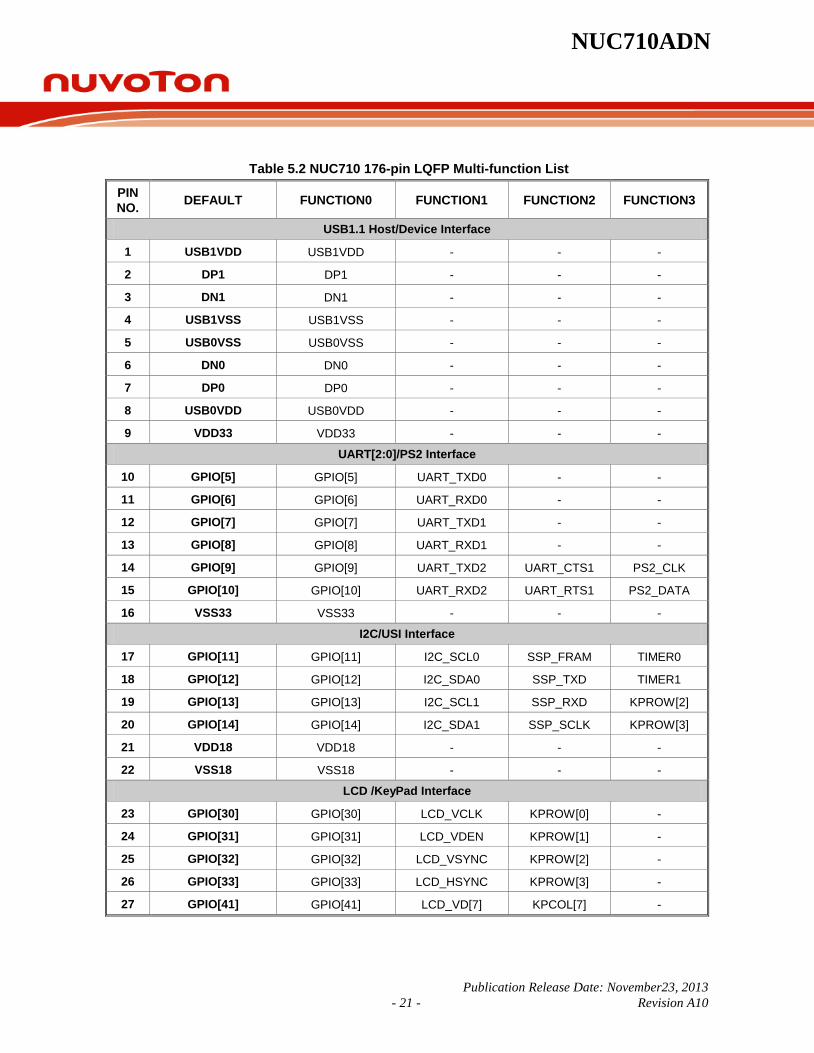
Table 5.2 NUC710 176-pin LQFP Multi-function List
PIN NO. DEFAULT FUNCTION0 FUNCTION1 FUNCTION2 FUNCTION3
USB1.1 Host/Device Interface
1 USB1VDD USB1VDD - - -
2 DP1 DP1 - - -
3 DN1 DN1 - - -
4 USB1VSS USB1VSS - - -
5 USB0VSS USB0VSS - - -
6 DN0 DN0 - - -
7 DP0 DP0 - - -
8 USB0VDD USB0VDD - - -
9 VDD33 VDD33 - - -
UART[2:0]/PS2 Interface 10 GPIO[5] GPIO[5] UART_TXD0 - -
11 GPIO[6] GPIO[6] UART_RXD0 - -
12 GPIO[7] GPIO[7] UART_TXD1 - -
13 GPIO[8] GPIO[8] UART_RXD1 - -
14 GPIO[9] GPIO[9] UART_TXD2 UART_CTS1 PS2_CLK
15 GPIO[10] GPIO[10] UART_RXD2 UART_RTS1 PS2_DATA
16 VSS33 VSS33 - - -
I2C/USI Interface 17 GPIO[11] GPIO[11] I2C_SCL0 SSP_FRAM TIMER0
18 GPIO[12] GPIO[12] I2C_SDA0 SSP_TXD TIMER1
19 GPIO[13] GPIO[13] I2C_SCL1 SSP_RXD KPROW[2]
20 GPIO[14] GPIO[14] I2C_SDA1 SSP_SCLK KPROW[3]
21 VDD18 VDD18 - - -
22 VSS18 VSS18 - - -
LCD /KeyPad Interface 23 GPIO[30] GPIO[30] LCD_VCLK KPROW[0] -
24 GPIO[31] GPIO[31] LCD_VDEN KPROW[1] -
25 GPIO[32] GPIO[32] LCD_VSYNC KPROW[2] -
26 GPIO[33] GPIO[33] LCD_HSYNC KPROW[3] -
27 GPIO[41] GPIO[41] LCD_VD[7] KPCOL[7] -
NUC710ADN
Publication Release Date: November235, 2013 - 22 - Revision A10
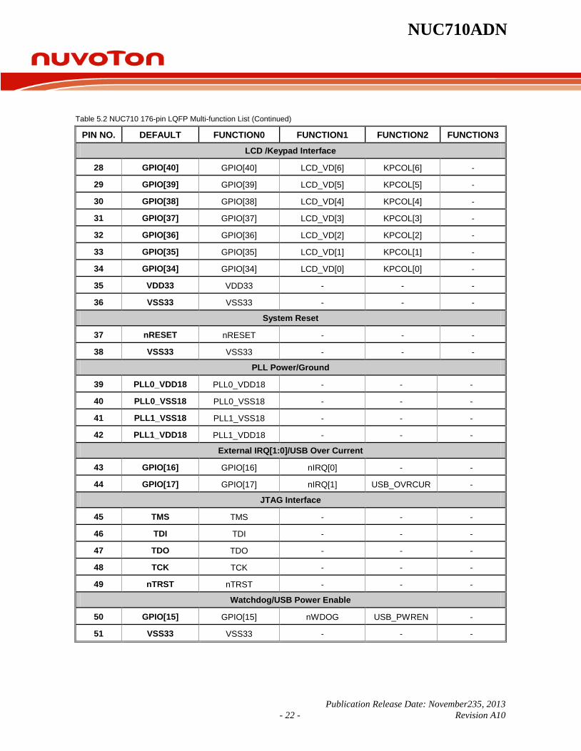
Table 5.2 NUC710 176-pin LQFP Multi-function List (Continued)
PIN NO. DEFAULT FUNCTION0 FUNCTION1 FUNCTION2 FUNCTION3
LCD /Keypad Interface
28 GPIO[40] GPIO[40] LCD_VD[6] KPCOL[6] -
29 GPIO[39] GPIO[39] LCD_VD[5] KPCOL[5] -
30 GPIO[38] GPIO[38] LCD_VD[4] KPCOL[4] -
31 GPIO[37] GPIO[37] LCD_VD[3] KPCOL[3] -
32 GPIO[36] GPIO[36] LCD_VD[2] KPCOL[2] -
33 GPIO[35] GPIO[35] LCD_VD[1] KPCOL[1] -
34 GPIO[34] GPIO[34] LCD_VD[0] KPCOL[0] -
35 VDD33 VDD33 - - -
36 VSS33 VSS33 - - -
System Reset
37 nRESET nRESET - - -
38 VSS33 VSS33 - - -
PLL Power/Ground
39 PLL0_VDD18 PLL0_VDD18 - - -
40 PLL0_VSS18 PLL0_VSS18 - - -
41 PLL1_VSS18 PLL1_VSS18 - - -
42 PLL1_VDD18 PLL1_VDD18 - - -
External IRQ[1:0]/USB Over Current
43 GPIO[16] GPIO[16] nIRQ[0] - -
44 GPIO[17] GPIO[17] nIRQ[1] USB_OVRCUR -
JTAG Interface
45 TMS TMS - - -
46 TDI TDI - - -
47 TDO TDO - - -
48 TCK TCK - - -
49 nTRST nTRST - - -
Watchdog/USB Power Enable
50 GPIO[15] GPIO[15] nWDOG USB_PWREN -
51 VSS33 VSS33 - - -
NUC710ADN
Publication Release Date: November23, 2013 - 23 - Revision A10
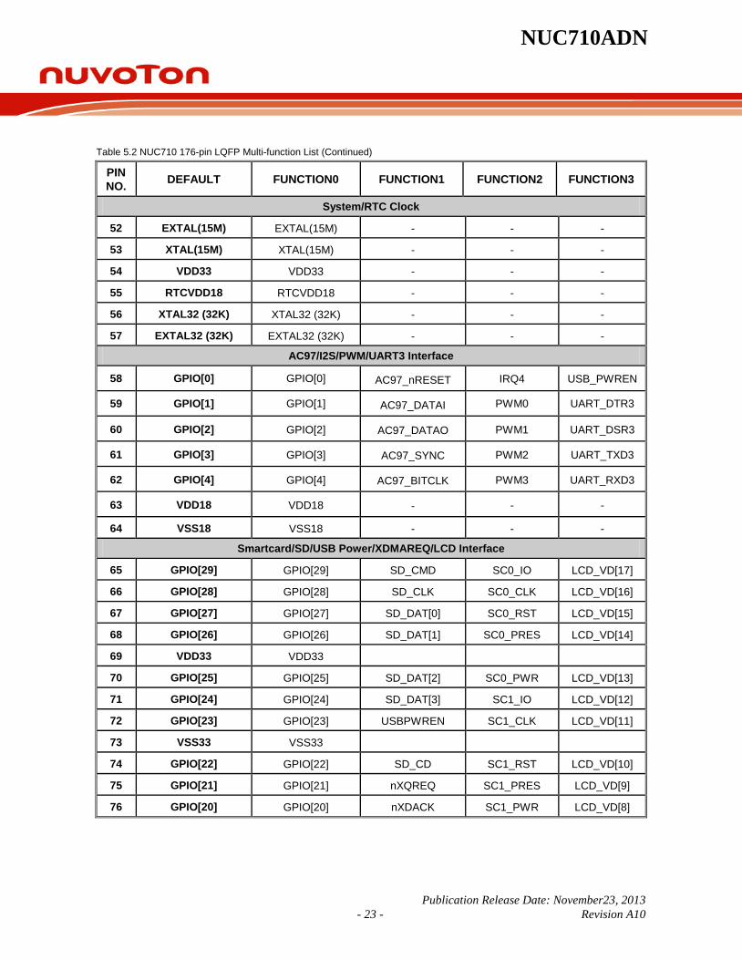
Table 5.2 NUC710 176-pin LQFP Multi-function List (Continued)
PIN NO. DEFAULT FUNCTION0 FUNCTION1 FUNCTION2 FUNCTION3
System/RTC Clock
52 EXTAL(15M) EXTAL(15M) - - -
53 XTAL(15M) XTAL(15M) - - -
54 VDD33 VDD33 - - -
55 RTCVDD18 RTCVDD18 - - -
56 XTAL32 (32K) XTAL32 (32K) - - -
57 EXTAL32 (32K) EXTAL32 (32K) - - -
AC97/I2S/PWM/UART3 Interface
58 GPIO[0] GPIO[0] AC97_nRESET IRQ4 USB_PWREN
59 GPIO[1] GPIO[1] AC97_DATAI PWM0 UART_DTR3
60 GPIO[2] GPIO[2] AC97_DATAO PWM1 UART_DSR3
61 GPIO[3] GPIO[3] AC97_SYNC PWM2 UART_TXD3
62 GPIO[4] GPIO[4] AC97_BITCLK PWM3 UART_RXD3
63 VDD18 VDD18 - - -
64 VSS18 VSS18 - - -
Smartcard/SD/USB Power/XDMAREQ/LCD Interface
65 GPIO[29] GPIO[29] SD_CMD SC0_IO LCD_VD[17]
66 GPIO[28] GPIO[28] SD_CLK SC0_CLK LCD_VD[16]
67 GPIO[27] GPIO[27] SD_DAT[0] SC0_RST LCD_VD[15]
68 GPIO[26] GPIO[26] SD_DAT[1] SC0_PRES LCD_VD[14]
69 VDD33 VDD33
70 GPIO[25] GPIO[25] SD_DAT[2] SC0_PWR LCD_VD[13]
71 GPIO[24] GPIO[24] SD_DAT[3] SC1_IO LCD_VD[12]
72 GPIO[23] GPIO[23] USBPWREN SC1_CLK LCD_VD[11]
73 VSS33 VSS33
74 GPIO[22] GPIO[22] SD_CD SC1_RST LCD_VD[10]
75 GPIO[21] GPIO[21] nXQREQ SC1_PRES LCD_VD[9]
76 GPIO[20] GPIO[20] nXDACK SC1_PWR LCD_VD[8]

NUC710ADN
Publication Release Date: November235, 2013 - 24 - Revision A10
Table 5.2 NUC710 176-pin LQFP Multi-function List (Continued)
PIN NO. DEFAULT FUNCTION0 FUNCTION1 FUNCTION2 FUNCTION3
Ethernet RMII/Keypad Interface
77 GPIO[42] GPIO[42] PHY_RXERR KPCOL[0] LCD_VD[8]
78 GPIO[43] GPIO[43] PHY_CRSDV KPCOL[1] LCD_VD[9]
79 GPIO[44] GPIO[44] PHY_RXD[0] KPCOL[2] LCD_VD[10]
80 VSS33 VSS33 - - -
81 GPIO[45] GPIO[45] PHY_RXD[1] KPCOL[3] LCD_VD[11]
82 GPIO[46] GPIO[46] PHY_REFCLK KPCOL[4] LCD_VD[12]
83 GPIO[47] GPIO[47] PHY_TXEN KPCOL[5] LCD_VD[13]
84 GPIO[48] GPIO[48] PHY_TXD[0] KPCOL[6] LCD_VD[14]
85 VDD33 VDD33 - -
86 GPIO[49] GPIO[49] PHY_TXD[1] KPCOL[7] LCD_VD[15]
87 GPIO[50] GPIO[50] PHY_MDIO KPROW[0] LCD_VD[16]
88 GPIO[51] GPIO[51] PHY_MDC KPROW[1] LCD_VD[17]
Memory Address/Data/Control
89 A[0] A[0] - - -
90 A[1] A[1] - - -
91 A[2] A[2] - - -
92 A[3] A[3] - - -
93 A[4] A[4] - - -
94 VSS33 VSS33 - - -
95 A[5] A[5] - - -
96 A[6] A[6] - - -
97 A[7] A[7] - - -
98 A[8] A[8] - - -
99 A[9] A[9] - - -
100 VDD33 VDD33 - - -
101 A[10] A[10] - - -
102 A[11] A[11] - - -
103 A[12] A[12] - - -
104 A[13] A[13] - - -
NUC710ADN
Publication Release Date: November23, 2013 - 25 - Revision A10
Table 5.2 NUC710 176-pin LQFP Multi-function List (Continued)
PIN NO. DEFAULT FUNCTION0 FUNCTION1 FUNCTION2 FUNCTION3
Memory Address/Data/Control
105 VSS18 VSS18 - - -
106 A[14] A[14] - - -
107 A[15] A[15] - - -
108 A[16] A[16] - - -
109 VDD18 VDD18 - - -
110 A[17] A[17] - - -
111 A[18] A[18] - - -
112 A[19] A[19] - - -
113 A[20] A[20] - - -
114 VSS33 VSS33 - - -
115 A[21] A[21] - - -
116 D[31] GPIO[67] D[31] LCD_VD[23] -
117 D[30] GPIO[66] D[30] LCD_VD[22] -
118 D[29] GPIO[65] D[29] LCD_VD[21] -
119 D[28] GPIO[64] D[28] LCD_VD[20] -
120 VDD33 VDD33 - - -
121 D[27] GPIO[63] D[27] LCD_VD[19] -
122 D[26] GPIO[62] D[26] LCD_VD[18] -
123 D[25] GPIO[61] D[25] LCD_VD[17] -
124 D[24] GPIO[60] D[24] LCD_VD[16] -
125 nECS[3] nECS[3] - - -
126 VSS33 VSS33 - - -
127 VDD33 VDD33 - - -
128 nECS[2] nECS[2] - - -
129 nECS[1] nECS[1] - - -
130 nECS[0] nECS[0] - - -
131 nOE nOE - - -
132 nWAIT GPIO[71] nWAIT IRQ5 -
133 nBTCS nBTCS - - -
134 MCKE MCKE - - -

NUC710ADN
Publication Release Date: November235, 2013 - 26 - Revision A10
Table 5.2 NUC710 176-pin LQFP Multi-function List (Continued)
PIN NO. DEFAULT FUNCTION0 FUNCTION1 FUNCTION2 FUNCTION3
Memory Address/Data/Control
135 nSCS[0] nSCS[0] - - -
136 nSCS[1] nSCS[1] - - -
137 nSRAS nSRAS - - -
138 nSCAS nSCAS - - -
139 VDD33 VDD33 - - -
140 MCLK MCLK - - -
141 VSS33 VSS33 - - -
142 nWE nWE - - -
143 nWBE_SDQM[0] nWBE_SDQM[0] - - -
144 nWBE_SDQM[1] nWBE_SDQM[1] - - -
145 nWBE_SDQM[2] GPIO[68] nWBE_SDQM[2] - -
146 nWBE_SDQM[3] GPIO[69] nWBE_SDQM[3] - -
147 GPIO[18] GPIO[18] nIRQ[2] - -
148 GPIO[19] GPIO[19] nIRQ[3] - -
149 GPIO[59] GPIO[59] D[23] LCD_VD[15] -
150 D[22] GPIO[58] D[22] LCD_VD[14] -
151 D[21] GPIO[57] D[21] LCD_VD[13] -
152 D[20] GPIO[56] D[20] LCD_VD[12] -
152 D[20] GPIO[56] D[20] LCD_VD[12] -
153 D[19] GPIO[55] D[19] LCD_VD[11] -
154 D[18] GPIO[54] D[18] LCD_VD[10] -
155 D[17] GPIO[53] D[17] LCD_VD[9] -
156 D[16] GPIO[52] D[16] LCD_VD[8] -
157 VSS18 VSS18 - - -
158 D[15] D[15] - - -
159 D[14] D[14] - - -
160 VDD18 VDD18 - - -
161 D[13] D[13] - - -
162 D[12] D[12] - - -
NUC710ADN
Publication Release Date: November23, 2013 - 27 - Revision A10
Table 5.2 NUC710 176-pin LQFP Multi-function List (Continued)
PIN NO. DEFAULT FUNCTION0 FUNCTION1 FUNCTION2 FUNCTION3
Memory Address/Data/Control
163 D[11] D[11] - - -
164 D[10] D[10] - - -
165 VDD33 VDD33 - - -
166 D[9] D[9] - - -
167 D[8] D[8] - - -
168 D[7] D[7] - - -
169 D[6] D[6] - - -
170 D[5] D[5] - - -
171 VSS33 VSS33 - - -
172 D[4] D[4] - - -
173 D[3] D[3] - - -
174 D[2] D[2] - - -
175 D[1] D[1] - - -
176 D[0] D[0] - - -
NUC710ADN
Publication Release Date: November235, 2013 - 28 - Revision A10
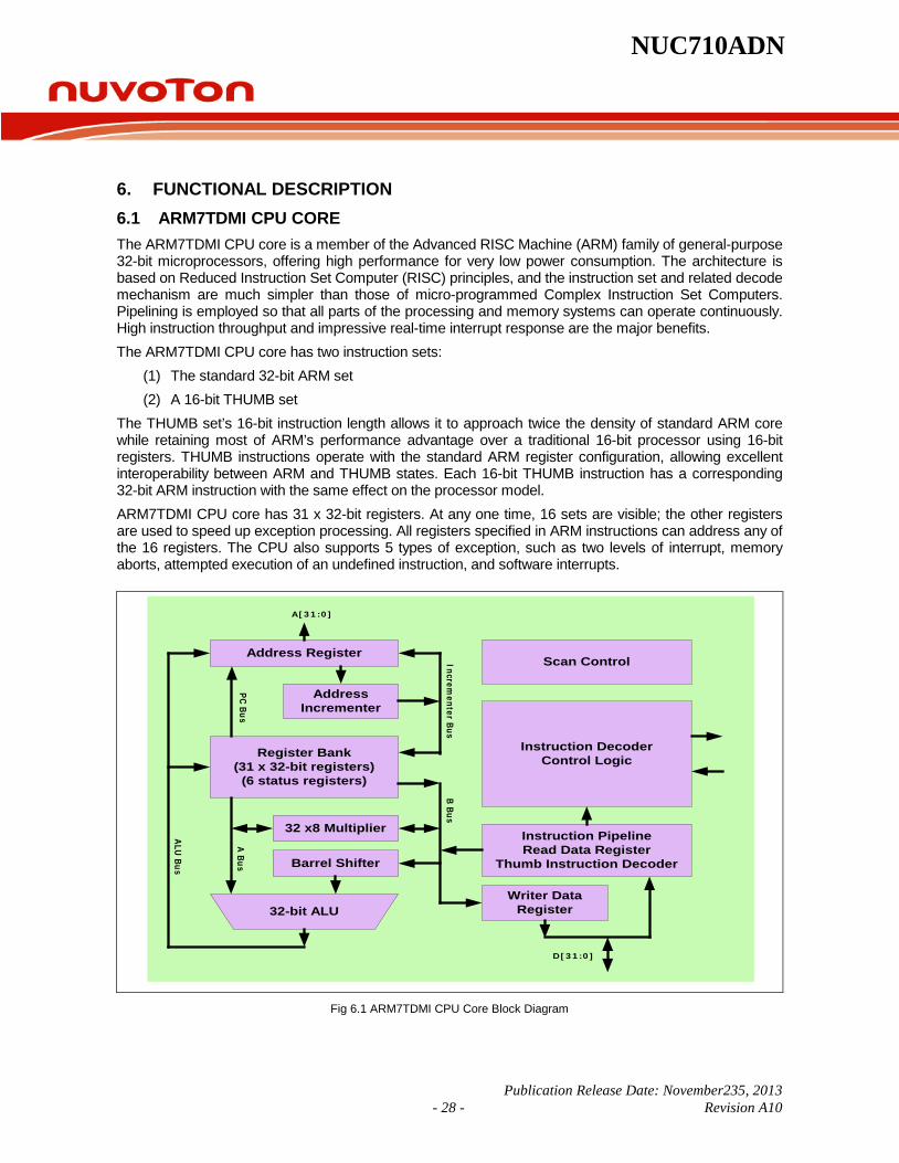
6. FUNCTIONAL DESCRIPTION 6.1 ARM7TDMI CPU CORE The ARM7TDMI CPU core is a member of the Advanced RISC Machine (ARM) family of general-purpose 32-bit microprocessors, offering high performance for very low power consumption. The architecture is based on Reduced Instruction Set Computer (RISC) principles, and the instruction set and related decode mechanism are much simpler than those of micro-programmed Complex Instruction Set Computers. Pipelining is employed so that all parts of the processing and memory systems can operate continuously. High instruction throughput and impressive real-time interrupt response are the major benefits. The ARM7TDMI CPU core has two instruction sets:
(1) The standard 32-bit ARM set (2) A 16-bit THUMB set
The THUMB set’s 16-bit instruction length allows it to approach twice the density of standard ARM core while retaining most of ARM’s performance advantage over a traditional 16-bit processor using 16-bit registers. THUMB instructions operate with the standard ARM register configuration, allowing excellent interoperability between ARM and THUMB states. Each 16-bit THUMB instruction has a corresponding 32-bit ARM instruction with the same effect on the processor model. ARM7TDMI CPU core has 31 x 32-bit registers. At any one time, 16 sets are visible; the other registers are used to speed up exception processing. All registers specified in ARM instructions can address any of the 16 registers. The CPU also supports 5 types of exception, such as two levels of interrupt, memory aborts, attempted execution of an undefined instruction, and software interrupts.
Address Register
AddressIncrementer
Barrel Shifter
Register Bank(31 x 32-bit registers)
(6 status registers)
32 x8 Multiplier
32-bit ALUWriter Data
Register
Instruction PipelineRead Data Register
Thumb Instruction Decoder
Instruction DecoderControl Logic
Scan Control
B Bus
A Bus
ALU Bus
PC Bus
Incrementer Bus
A[31:0]
D[31:0]
Fig 6.1 ARM7TDMI CPU Core Block Diagram

NUC710ADN
Publication Release Date: November23, 2013 - 29 - Revision A10
6.2 System Manager 6.2.1 Overview The NUC710 System Manager has the following functions. System memory map Data bus connection with external memory Product identifier register Bus arbitration PLL module Clock select and power saving control register Power-On setting
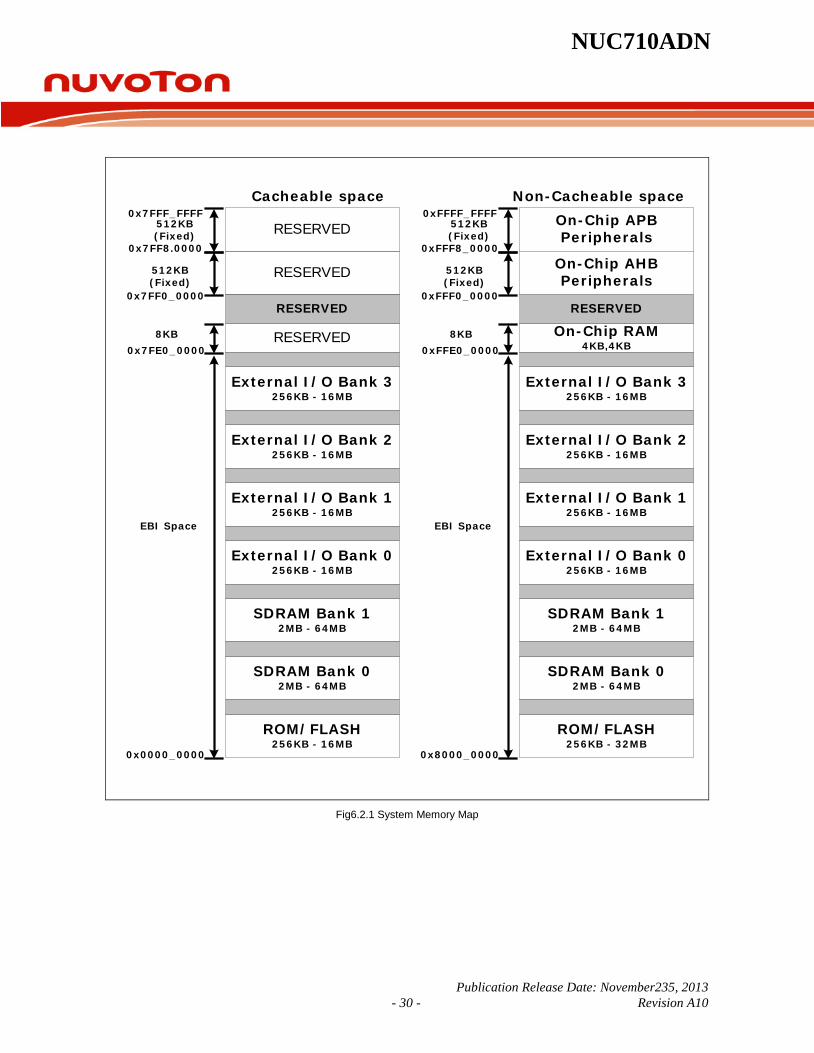
6.2.2 System Memory Map NUC710 provides 2G bytes cacheable address space and the other 2G bytes are non-cacheable. The On-Chip Peripherals bank is on 1M bytes top of the space (0xFFF0_0000 – 0xFFFF_FFFF) and the On-Chip RAM bank’s start address is 0xFFE0.0000, the other banks can be located anywhere (cacheable space: 0x0000_0000 ~ 0x7FDF_FFFF if Cache ON; non-cacheable space: 0x8000_0000 ~ 0xFFDF_FFFF). The size and location of each bank is determined by the register settings for “current bank base address pointer” and “current bank size”. Please note that when setting the bank control registers, the address boundaries of consecutive banks must not overlap. Except for On-Chip Peripherals and On-Chip RAM, the start address of each memory bank is not fixed. You can use bank control registers to assign a specific bank start address by setting the bank’s base pointer (13 bits). The address resolution is 256K bytes. The bank’s start address is defined as “base pointer << 18” and the bank’s size is “current bank size”. In the event of an access requested to an address outside any programmed bank size, an abort signal is generated. The maximum accessible memory size of each external IO bank is 16M bytes (by word format), and 64M bytes on each SDRAM bank.
NUC710ADN
Publication Release Date: November235, 2013 - 30 - Revision A10
ROM/FLASH256KB - 16MB
SDRAM Bank 02MB - 64MB
SDRAM Bank 12MB - 64MB
External I/O Bank 0256KB - 16MB
External I/O Bank 1256KB - 16MB
External I/O Bank 2256KB - 16MB
External I/O Bank 3256KB - 16MB
RESERVED
RESERVED
8KB
512KB(Fixed)
0x7FF8.0000
0x0000_0000
0x7FFF_FFFF
RESERVED
0x7FE0_0000
RESERVED512KB(Fixed)
0x7FF0_0000
EBI Space
ROM/FLASH256KB - 32MB
SDRAM Bank 02MB - 64MB
SDRAM Bank 12MB - 64MB
External I/O Bank 0256KB - 16MB
External I/O Bank 1256KB - 16MB
External I/O Bank 2256KB - 16MB
External I/O Bank 3256KB - 16MB
On-Chip RAM4KB,4KB
On-Chip APBPeripherals
8KB
512KB(Fixed)
0xFFF8_0000
0x8000_0000
0xFFFF_FFFF
RESERVED
0xFFE0_0000
On-Chip AHBPeripherals
512KB(Fixed)
0xFFF0_0000
EBI Space
Cacheable space Non-Cacheable space
Fig6.2.1 System Memory Map

NUC710ADN
Publication Release Date: November23, 2013 - 31 - Revision A10
Table 6.2.1 On-Chip Peripherals Memory Map
BASE ADDRESS DESCRIPTION AHB Peripherals
0xFFF0_0000 Product Identifier Register (PDID) 0xFFF0_0004 Arbitration Control Register (ARBCON) 0xFFF0_0008 PLL Control Register 0(PLLCON0) 0xFFF0_000C Clock Select Register (CLKSEL) 0xFFF0_0010 PLL Control Register 1 (PLLCON1) 0xFFF0_0014 Audio IIS Clock Control Register (I2SCKCON) 0xFFF0_0020 IRQ Wakeup Control Register (IRQWAKEUPCON) 0xFFF0_0024 IRQ Wakeup Flag Register (IRQWAKEFLAG) 0xFFF0_0028 Power Manager Control Register (PMCON) 0xFFF0_0030 USB Transceiver Control Register (USBTXRCON) 0xFFF0_1000 EBI Control Register (EBICON) Control Registers 0xFFF0_1004 ROM/FLASH (ROMCON) Control Registers 0xFFF0_1008 SDRAM bank 0 – 1 Control Registers 0xFFF0_1018 External I/O 0 – 3 Control Registers 0xFFF0_2000 Cache Controller Control Registers 0xFFF0_3000 Ethernet MAC Controller Control Registers 0xFFF0_4000 GDMA 0 – 1 Control Registers 0xFFF0_5000 USB Host Controller Control Registers 0xFFF0_6000 USB Device Controller Control Registers 0xFFF0_7000 SD Host Controller Control Registers 0xFFF0_8000 LCD Controller Control Registers 0xFFF0_9000 AC97/I2S Controller Control Registers
APB Peripherals 0xFFF8_0000 UART 0 (Tx, Rx for console) 0xFFF8_0100 UART 1 (Tx, Rx, for Bluetooth) 0xFFF8_0200 UART 2 (Bluetooth CTS, RTS/ IrDA Tx, Rx) 0xFFF8_0300 UART 3 (micro-print DTR, DTS, Tx, Rx) 0xFFF8_1000 Timer 0 – 1, WDOG Timer 0xFFF8_2000 Interrupt Controller 0xFFF8_3000 GPIO 0xFFF8_4000 Real Time Clock Controller Control Registers (RTC) 0xFFF8_5000 Smart Card Host Interface Control Registers (SCHI) 0xFFF8_6000 I2C-0 Control Registers 0xFFF8_6100 I2C-1 Control Registers 0xFFF8_6200 USI Control Registers

NUC710ADN
Publication Release Date: November235, 2013 - 32 - Revision A10
Table 6.2.1 On-Chip Peripherals Memory Map (Continued)
BASE ADDRESS DESCRIPTION APB Peripherals
0xFFF8_7000 Pulse Width Modulation (PWM) Control Registers 0xFFF8_8000 Keypad Interface Control Register (KPI) 0xFFF8_9000 PS2 Control Registers
6.2.3 Address Bus Generation The NUC710 address bus generation depends on the required data bus width of each memory bank. The data bus width is determined by DBWD bits in each bank’s control register. The maximum accessible memory size of each external IO bank is 16M bytes.
Table 6.2.2 Address Bus Generation Guidelines DATA BUS EXTERNAL ADDRESS PINS MAXIMUM ACCESSIBLE MEMORY
SIZE WIDTH A [21:0]
8-bit A21 – A0 (Internal) 4M bytes
16-bit A22 – A1 (Internal) 4M half-words
32-bit A23 – A2 (Internal) 4M words
6.2.4 Data Bus Connection with External Memory
6.2.4.1 Memory formats The NUC710 can be configured to operate in big-endian or little-endian via pull-up or pull-down register on the external data bus, pin D14. If D14 is pulled up then little-endian is used, otherwise, big-endian mode is set.
Little-endian In little-endian format, the lowest addressed byte in a word is considered the least significant byte of the word and the highest addressable byte is the most significant. So the byte at address 0 of the memory system connects to data lines 7 through 0. For a word aligned address A, Fig6.2.2 shows how the word at address A, the half-word at addresses A and A+2, and the bytes at addresses A, A+1, A+2, and A+3 map to each other when pin D14 is High.
31 30 29 28 27 26 25 24 23 22 21 20 19 18 17 16 15 14 13 12 11 10 9 8 7 6 5 4 3 2 1 0
Word at address A
Half-word at address A+2 Half-word at address A
Byte at address A+3 Byte at address A+2 Byte at address A+1 Byte at address A
Fig6.2.2 Little-endian addresses of bytes and half-words within words

NUC710ADN
Publication Release Date: November23, 2013 - 33 - Revision A10
Big-endian In Big-endian format, NUC710 stores the most significant byte of a word at the lowest numbered byte, and the least significant byte at the highest-numbered byte. So the byte at address 0 of the memory system connects to data lines 31 through 24. For a word aligned address A, Fig6.2.3 shows how the word at address A, the half-word at addresses A and A+2, and the bytes at addresses A, A+1, A+2, and A+3 map to each other when pin D14 is Low.
31 30 29 28 27 26 25 24 23 22 21 20 19 18 17 16 15 14 13 12 11 10 9 8 7 6 5 4 3 2 1 0
Word at address A
Half-word at address A Half-word at address A+2
Byte at address A Byte at address A+1 Byte at address A+2 Byte at address A+3
Fig6.2.3 Big-endian addresses of bytes and half-words within words
6.2.4.2 Connecting External Memory of Various Data Widths The system diagram for connecting NUC710 to external memory is shown in Fig6.2.4. The following tables (Table6.2.3 through Table6.2.14) show the program/data path between CPU register and external memory using little / big-endian and word/half-word/byte access.
Fig6.2.4 Address/Data bus connection with external memory
NUC710ADN

NUC710ADN
Publication Release Date: November235, 2013 - 34 - Revision A10
Fig6.2.5 CPU registers Read/Write with external memory
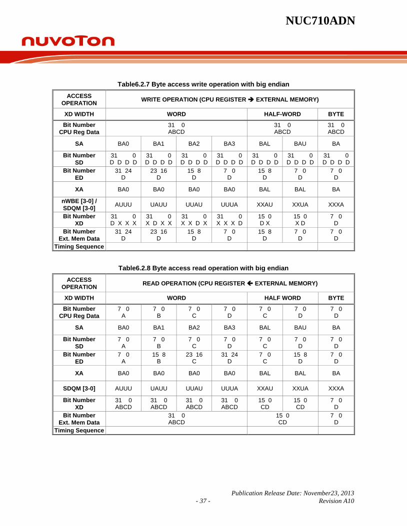
Table 6.2.3 and Table 6.2.4 Using big-endian and word access, Program/Data path between register and external memory WA = Address whose LSB is 0,4,8,C X = Don’t care nWBE [3-0] / SDQM [3-0] = A means active and U means inactive
Table6.2.3 Word access write operation with big endian ACCESS
OPERATION WRITE OPERATION (CPU REGISTER EXTERNAL MEMORY)
XD WIDTH WORD HALF WORD BYTE
Bit Number CPU Reg Data
31 0 ABCD
31 0 ABCD
31 0 ABCD
SA WA WA WA Bit Number
SD 31 0 ABCD
31 0 AB CD
31 0 A B C D
Bit Number ED
31 0 ABCD
15 0 AB
15 0 CD
7 0 A
7 0 B
7 0 C
7 0 D
XA WA WA WA+2 WA WA+1 WA+2 WA+3
nWBE [3-0] / SDQM [3-0] AAAA XXAA XXAA XXXA XXXA XXXA XXXA
Bit Number XD
31 0 ABCD
15 0 AB
15 0 CD
7 0 A
7 0 B
7 0 C
7 0 D
Bit Number Ext. Mem Data
31 0 ABCD
15 0 AB
15 0 CD
7 0 A
7 0 B
7 0 C
7 0 D
Timing Sequence 1st write 2nd write 1st write 2nd write 3rd write 4th write

NUC710ADN
Publication Release Date: November23, 2013 - 35 - Revision A10
Table6.2.4 Word access read operation with big endian
ACCESS OPERATION READ OPERATION (CPU REGISTER EXTERNAL MEMORY)
XD WIDTH WORD HALF WORD BYTE
Bit Number CPU Reg Data
31 0 ABCD
31 0 CDAB
31 0 DCBA
SA WA WA WA Bit Number
SD 31 0 ABCD
31 0 CD AB
31 0 D C B A
Bit Number ED
31 0 ABCD
31 0 CD XX
31 0 CD AB
31 0 D X X X
31 0 D C X X
31 0 D C B X
31 0 D C B A
XA WA WA WA+2 WA WA+1 WA+2 WA+3
SDQM [3-0] AAAA XXAA XXAA XXXA XXXA XXXA XXXA
Bit Number XD
31 0 ABCD
15 0 CD
15 0 AB
7 0 D
7 0 C
7 0 B
7 0 A
Bit Number Ext. Mem Data
31 0 ABCD
15 0 CD
15 0 AB
7 0 D
7 0 C
7 0 B
7 0 A
Timing Sequence 1st read 2nd read 1st read 2nd read 3rd read 4th read
Table 6.2.5 and Table 6.2.6 Using big-endian and half-word access, Program/Data path between register and external memory. HA = Address whose LSB is 0,2,4,6,8,A,C,E HAL = Address whose LSB is 0,4,8,C HAU = Address whose LSB is 2,6,A,E X = Don’t care nWBE [3-0] / SDQM [3-0] = A means active and U means inactive
Table6.2.5 Half-word access write operation with big endian
ACCESS OPERATION WRITE OPERATION (CPU REGISTER EXTERNAL MEMORY)
XD WIDTH WORD HALF WORD BYTE
Bit Number CPU Reg Data
31 0 ABCD
31 0 ABCD
31 0 ABCD
SA HAL HAU HA HA
Bit Number SD
31 0 CD CD
31 0 CD CD
31 0 CD CD
31 0 CD CD
31 0 CD CD
Bit Number ED
31 0 CD CD
31 0 CD CD
31 0 CD CD
7 0 C
7 0 D
XA HAL HAL HA HA HA+1
nWBE [3-0] / SDQM [3-0] AAUU UUAA XXAA XXXA XXXA
Bit Number XD
31 0 CD CD
31 0 CD CD
15 0 CD
7 0 C
7 0 D
Bit Number Ext. Mem Data
31 16 CD
15 0 CD
15 0 CD
7 0 C
7 0 D
Timing Sequence 1st write 2nd write

NUC710ADN
Publication Release Date: November235, 2013 - 36 - Revision A10
Table6.2.6 Half-word access read operation with big endian
ACCESS OPERATION READ OPERATION (CPU REGISTER EXTERNAL MEMORY)
XD WIDTH WORD HALF WORD BYTE
Bit Number CPU Reg Data
15 0 AB
15 0 CD
15 0 CD
15 0 DC
SA HAL HAU HA HA
Bit Number SD
15 0 AB
15 0 CD
15 0 CD
15 0 DC
Bit Number ED
15 0 AB
15 0 CD
15 0 CD
15 0 DX
15 0 DC
XA HAL HAL HA HA HA+1
SDQM [3-0] AAUU UUAA XXAA XXXA XXXA
Bit Number XD
31 0 AB CD
31 0 AB CD
15 0 CD
7 0 D
7 0 C
Bit Number Ext. Mem Data
31 0 ABCD
15 0 CD
7 0 D
7 0 C
Timing Sequence 1st read 2nd read
Table 6.2.7 and Table 6.2.8 Using big-endian and byte access, Program/Data path between register and external memory. BA = Address whose LSB is 0,1,2,3,4,5,6,7,8,9,A,B,C,D,E,F BAL = Address whose LSB is 0,2,4,6,8,A,C,E BAU = Address whose LSB is 1,3,5,7,9,B,D,F BA0 = Address whose LSB is 0,4,8,C BA1 = Address whose LSB is 1,5,9,D BA2 = Address whose LSB is 2,6,A,E BA3 = Address whose LSB is 3,7,B,F
NUC710ADN
Publication Release Date: November23, 2013 - 37 - Revision A10
Table6.2.7 Byte access write operation with big endian ACCESS
OPERATION WRITE OPERATION (CPU REGISTER EXTERNAL MEMORY)
XD WIDTH WORD HALF-WORD BYTE
Bit Number CPU Reg Data
31 0 ABCD
31 0 ABCD
31 0 ABCD
SA BA0 BA1 BA2 BA3 BAL BAU BA
Bit Number SD
31 0 D D D D
31 0 D D D D
31 0 D D D D
31 0 D D D D
31 0 D D D D
31 0 D D D D
31 0 D D D D
Bit Number ED
31 24 D
23 16 D
15 8 D
7 0 D
15 8 D
7 0 D
7 0 D
XA BA0 BA0 BA0 BA0 BAL BAL BA
nWBE [3-0] / SDQM [3-0] AUUU UAUU UUAU UUUA XXAU XXUA XXXA
Bit Number XD
31 0 D X X X
31 0 X D X X
31 0 X X D X
31 0 X X X D
15 0 D X
15 0 X D
7 0 D
Bit Number Ext. Mem Data
31 24 D
23 16 D
15 8 D
7 0 D
15 8 D
7 0 D
7 0 D
Timing Sequence
Table6.2.8 Byte access read operation with big endian
ACCESS OPERATION READ OPERATION (CPU REGISTER EXTERNAL MEMORY)
XD WIDTH WORD HALF WORD BYTE
Bit Number CPU Reg Data
7 0 A
7 0 B
7 0 C
7 0 D
7 0 C
7 0 D
7 0 D
SA BA0 BA1 BA2 BA3 BAL BAU BA
Bit Number SD
7 0 A
7 0 B
7 0 C
7 0 D
7 0 C
7 0 D
7 0 D
Bit Number ED
7 0 A
15 8 B
23 16 C
31 24 D
7 0 C
15 8 D
7 0 D
XA BA0 BA0 BA0 BA0 BAL BAL BA
SDQM [3-0] AUUU UAUU UUAU UUUA XXAU XXUA XXXA
Bit Number XD
31 0 ABCD
31 0 ABCD
31 0 ABCD
31 0 ABCD
15 0 CD
15 0 CD
7 0 D
Bit Number Ext. Mem Data
31 0 ABCD
15 0 CD
7 0 D
Timing Sequence
NUC710ADN
Publication Release Date: November235, 2013 - 38 - Revision A10
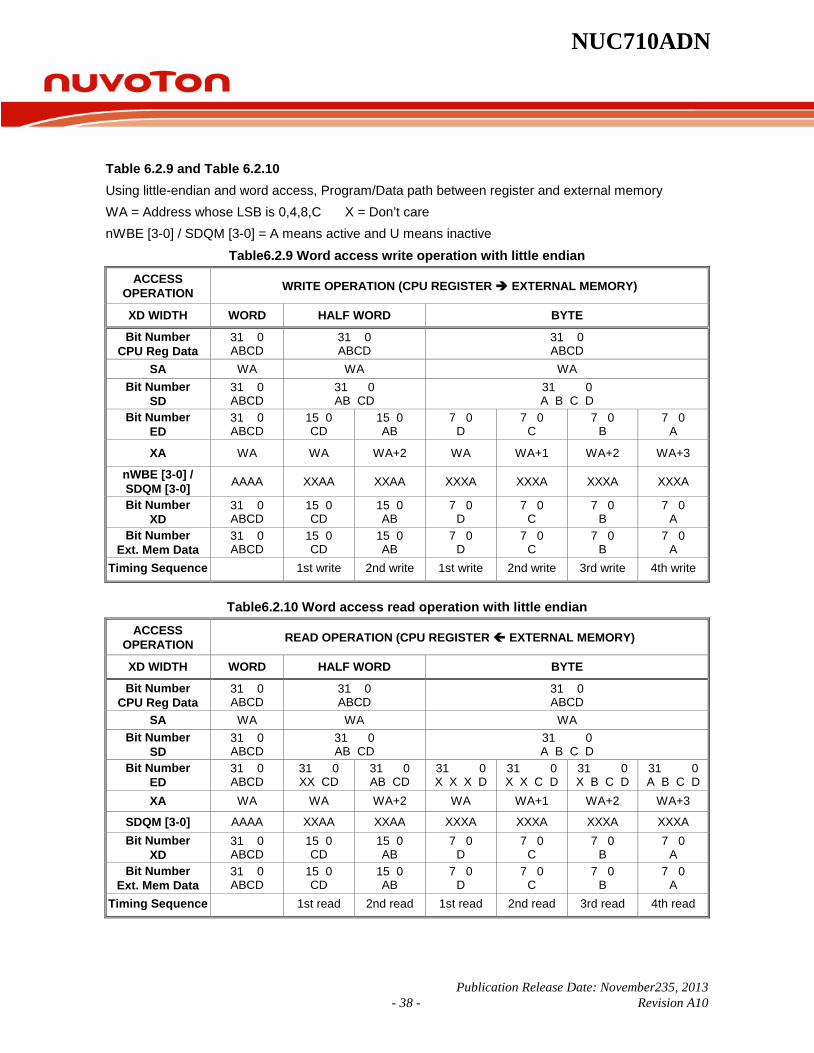
Table 6.2.9 and Table 6.2.10 Using little-endian and word access, Program/Data path between register and external memory WA = Address whose LSB is 0,4,8,C X = Don’t care nWBE [3-0] / SDQM [3-0] = A means active and U means inactive
Table6.2.9 Word access write operation with little endian ACCESS
OPERATION WRITE OPERATION (CPU REGISTER EXTERNAL MEMORY)
XD WIDTH WORD HALF WORD BYTE
Bit Number CPU Reg Data
31 0 ABCD
31 0 ABCD
31 0 ABCD
SA WA WA WA Bit Number
SD 31 0 ABCD
31 0 AB CD
31 0 A B C D
Bit Number ED
31 0 ABCD
15 0 CD
15 0 AB
7 0 D
7 0 C
7 0 B
7 0 A
XA WA WA WA+2 WA WA+1 WA+2 WA+3
nWBE [3-0] / SDQM [3-0] AAAA XXAA XXAA XXXA XXXA XXXA XXXA
Bit Number XD
31 0 ABCD
15 0 CD
15 0 AB
7 0 D
7 0 C
7 0 B
7 0 A
Bit Number Ext. Mem Data
31 0 ABCD
15 0 CD
15 0 AB
7 0 D
7 0 C
7 0 B
7 0 A
Timing Sequence 1st write 2nd write 1st write 2nd write 3rd write 4th write
Table6.2.10 Word access read operation with little endian ACCESS
OPERATION READ OPERATION (CPU REGISTER EXTERNAL MEMORY)
XD WIDTH WORD HALF WORD BYTE
Bit Number CPU Reg Data
31 0 ABCD
31 0 ABCD
31 0 ABCD
SA WA WA WA Bit Number
SD 31 0 ABCD
31 0 AB CD
31 0 A B C D
Bit Number ED
31 0 ABCD
31 0 XX CD
31 0 AB CD
31 0 X X X D
31 0 X X C D
31 0 X B C D
31 0 A B C D
XA WA WA WA+2 WA WA+1 WA+2 WA+3
SDQM [3-0] AAAA XXAA XXAA XXXA XXXA XXXA XXXA Bit Number
XD 31 0 ABCD
15 0 CD
15 0 AB
7 0 D
7 0 C
7 0 B
7 0 A
Bit Number Ext. Mem Data
31 0 ABCD
15 0 CD
15 0 AB
7 0 D
7 0 C
7 0 B
7 0 A
Timing Sequence 1st read 2nd read 1st read 2nd read 3rd read 4th read

NUC710ADN
Publication Release Date: November23, 2013 - 39 - Revision A10
Table 6.2.11 and Table 6.2.12 Using little-endian and half-word access, Program/Data path between register and external memory. HA = Address whose LSB is 0,2,4,6,8,A,C,E HAL = Address whose LSB is 0,4,8,C HAU = Address whose LSB is 2,6,A,E X = Don’t care nWBE [3-0] / SDQM [3-0] = A means active and U means inactive
Table6.2.11 Half-word access write operation with little-endian
ACCESS OPERATION WRITE OPERATION (CPU REGISTER EXTERNAL MEMORY)
XD WIDTH WORD HALF WORD BYTE
Bit Number CPU Reg Data
31 0 ABCD
31 0 ABCD
31 0 ABCD
SA HAL HAU HA HA Bit Number
SD 31 0
CD CD 31 0
CD CD 31 0
CD CD 31 0
CD CD 31 0
CD CD Bit Number
ED 31 0
CD CD 31 0
CD CD 31 0
CD CD 7 0
D 7 0
C XA HAL HAL HA HA HA+1
nWBE [3-0] / SDQM [3-0] UUAA AAUU XXAA XXXA XXXA
Bit Number XD
31 0 CD CD
31 0 CD CD
15 0 CD
7 0 D
7 0 C
Bit Number Ext. Mem Data
15 0 CD
31 16 CD
15 0 CD
7 0 D
7 0 C
Timing Sequence 1st write 2nd write
Table6.2.12 Half-word access read operation with Little-endian
ACCESS OPERATION READ OPERATION (CPU REGISTER EXTERNAL MEMORY)
XD WIDTH WORD HALF WORD BYTE
Bit Number CPU Reg Data
15 0 CD
15 0 AB
15 0 CD
15 0 CD
SA HAL HAU HA HA
Bit Number SD
15 0 CD
15 0 AB
15 0 CD
15 0 CD
Bit Number ED
15 0 CD
15 0 AB
15 0 CD
15 0 XD
15 0 CD
XA HAL HAL HA HA HA+1
SDQM [3-0] UUAA AAUU XXAA XXXA XXXA Bit Number
XD 31 0 AB CD
31 0 AB CD
15 0 CD
7 0 D
7 0 C
Bit Number Ext. Mem Data
31 0 ABCD
15 0 CD
7 0 D
7 0 C
Timing Sequence 1st read 2nd read
Table 6.2.13 and Table 6.2.14
NUC710ADN
Publication Release Date: November235, 2013 - 40 - Revision A10
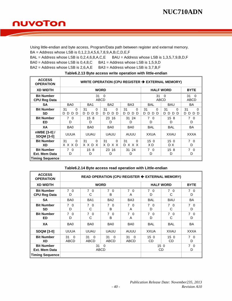
Using little-endian and byte access, Program/Data path between register and external memory. BA = Address whose LSB is 0,1,2,3,4,5,6,7,8,9,A,B,C,D,E,F BAL = Address whose LSB is 0,2,4,6,8,A,C,E BAU = Address whose LSB is 1,3,5,7,9,B,D,F BA0 = Address whose LSB is 0,4,8,C BA1 = Address whose LSB is 1,5,9,D BA2 = Address whose LSB is 2,6,A,E BA3 = Address whose LSB is 3,7,B,F
Table6.2.13 Byte access write operation with little-endian ACCESS
OPERATION WRITE OPERATION (CPU REGISTER EXTERNAL MEMORY)
XD WIDTH WORD HALF WORD BYTE Bit Number
CPU Reg Data 31 0 ABCD
31 0 ABCD
31 0 ABCD
SA BA0 BA1 BA2 BA3 BAL BAU BA Bit Number
SD 31 0 D D D D
31 0 D D D D
31 0 D D D D
31 0 D D D D
31 0 D D D D
31 0 D D D D
31 0 D D D D
Bit Number ED
7 0 D
15 8 D
23 16 D
31 24 D
7 0 D
15 8 D
7 0 D
XA BA0 BA0 BA0 BA0 BAL BAL BA nWBE [3-0] / SDQM [3-0] UUUA UUAU UAUU AUUU XXUA XXAU XXXA
Bit Number XD
31 0 X X X D
31 0 X X D X
31 0 X D X X
31 0 D X X X
15 0 X D
15 0 D X
7 0 D
Bit Number Ext. Mem Data
7 0 D
15 8 D
23 16 D
31 24 D
7 0 D
15 8 D
7 0 D
Timing Sequence
Table6.2.14 Byte access read operation with Little-endian ACCESS
OPERATION READ OPERATION (CPU REGISTER EXTERNAL MEMORY)
XD WIDTH WORD HALF WORD BYTE Bit Number
CPU Reg Data 7 0
D 7 0
C 7 0
B 7 0
A 7 0
D 7 0
C 7 0
D SA BA0 BA1 BA2 BA3 BAL BAU BA
Bit Number SD
7 0 D
7 0 C
7 0 B
7 0 A
7 0 D
7 0 C
7 0 D
Bit Number ED
7 0 D
7 0 C
7 0 B
7 0 A
7 0 D
7 0 C
7 0 D
XA BA0 BA0 BA0 BA0 BAL BAL BA
SDQM [3-0] UUUA UUAU UAUU AUUU XXUA XXAU XXXA Bit Number
XD 31 0 ABCD
31 0 ABCD
31 0 ABCD
31 0 ABCD
15 0 CD
15 0 CD
7 0 D
Bit Number Ext. Mem Data
31 0 ABCD
15 0 CD
7 0 D
Timing Sequence
NUC710ADN
Publication Release Date: November23, 2013 - 41 - Revision A10
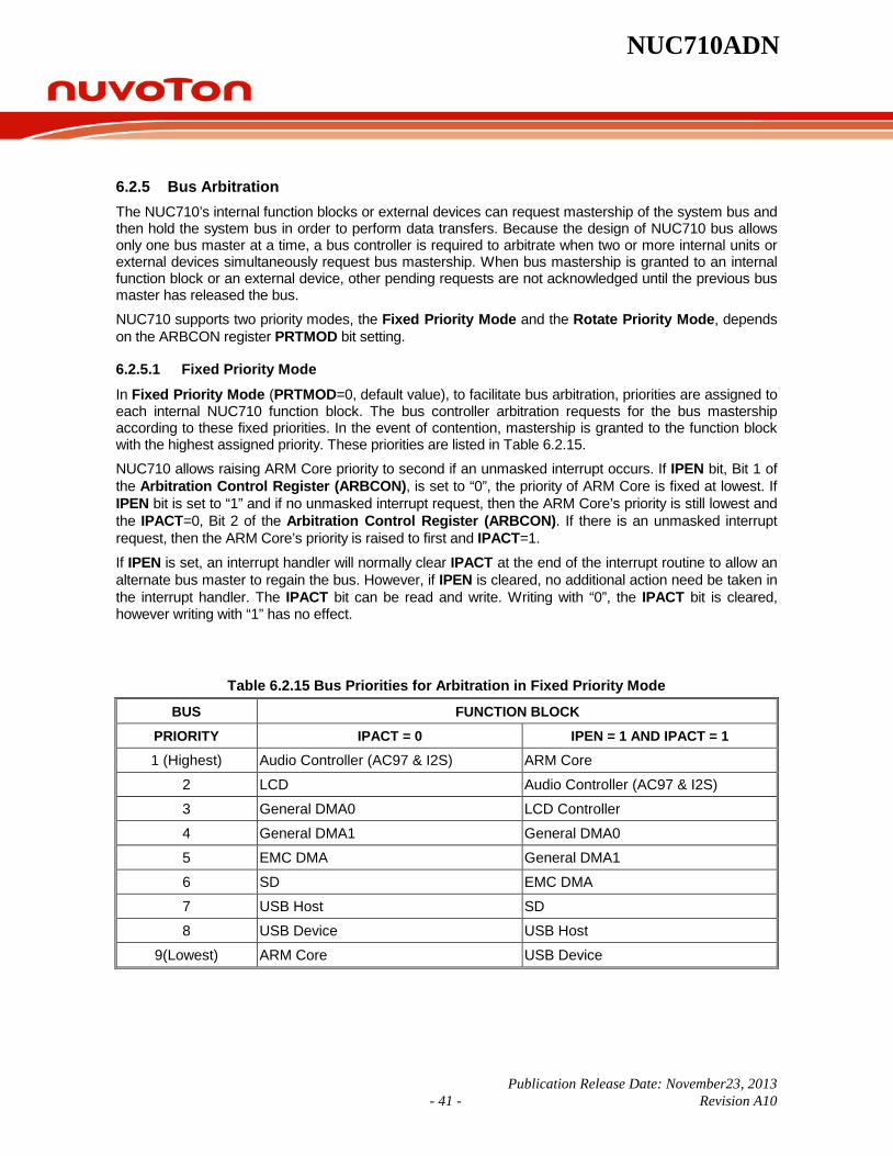
6.2.5 Bus Arbitration The NUC710’s internal function blocks or external devices can request mastership of the system bus and then hold the system bus in order to perform data transfers. Because the design of NUC710 bus allows only one bus master at a time, a bus controller is required to arbitrate when two or more internal units or external devices simultaneously request bus mastership. When bus mastership is granted to an internal function block or an external device, other pending requests are not acknowledged until the previous bus master has released the bus. NUC710 supports two priority modes, the Fixed Priority Mode and the Rotate Priority Mode, depends on the ARBCON register PRTMOD bit setting.
6.2.5.1 Fixed Priority Mode In Fixed Priority Mode (PRTMOD=0, default value), to facilitate bus arbitration, priorities are assigned to each internal NUC710 function block. The bus controller arbitration requests for the bus mastership according to these fixed priorities. In the event of contention, mastership is granted to the function block with the highest assigned priority. These priorities are listed in Table 6.2.15. NUC710 allows raising ARM Core priority to second if an unmasked interrupt occurs. If IPEN bit, Bit 1 of the Arbitration Control Register (ARBCON), is set to “0”, the priority of ARM Core is fixed at lowest. If IPEN bit is set to “1” and if no unmasked interrupt request, then the ARM Core’s priority is still lowest and the IPACT=0, Bit 2 of the Arbitration Control Register (ARBCON). If there is an unmasked interrupt request, then the ARM Core’s priority is raised to first and IPACT=1.
If IPEN is set, an interrupt handler will normally clear IPACT at the end of the interrupt routine to allow an alternate bus master to regain the bus. However, if IPEN is cleared, no additional action need be taken in the interrupt handler. The IPACT bit can be read and write. Writing with “0”, the IPACT bit is cleared, however writing with “1” has no effect.
Table 6.2.15 Bus Priorities for Arbitration in Fixed Priority Mode
BUS FUNCTION BLOCK
PRIORITY IPACT = 0 IPEN = 1 AND IPACT = 1
1 (Highest) Audio Controller (AC97 & I2S) ARM Core
2 LCD Audio Controller (AC97 & I2S)
3 General DMA0 LCD Controller
4 General DMA1 General DMA0
5 EMC DMA General DMA1
6 SD EMC DMA
7 USB Host SD
8 USB Device USB Host
9(Lowest) ARM Core USB Device
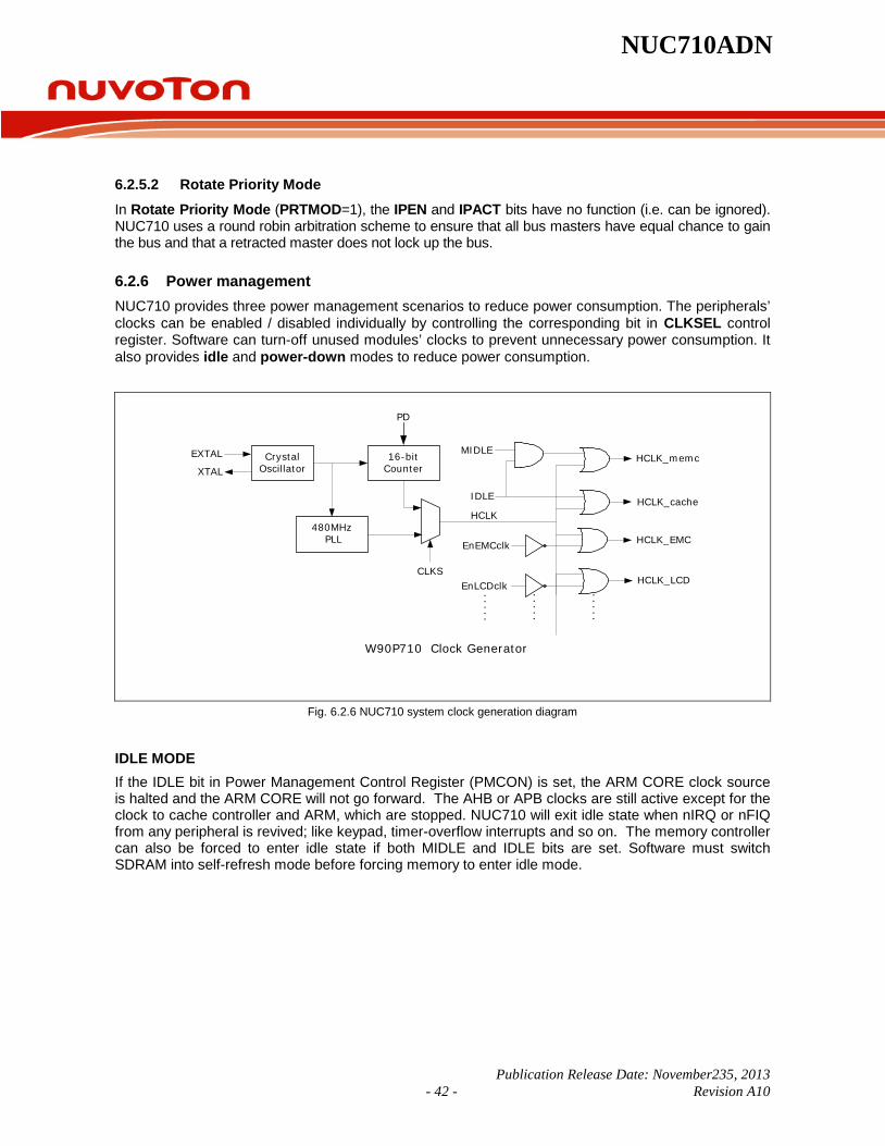
NUC710ADN
Publication Release Date: November235, 2013 - 42 - Revision A10
6.2.5.2 Rotate Priority Mode In Rotate Priority Mode (PRTMOD=1), the IPEN and IPACT bits have no function (i.e. can be ignored). NUC710 uses a round robin arbitration scheme to ensure that all bus masters have equal chance to gain the bus and that a retracted master does not lock up the bus.
6.2.6 Power management NUC710 provides three power management scenarios to reduce power consumption. The peripherals’ clocks can be enabled / disabled individually by controlling the corresponding bit in CLKSEL control register. Software can turn-off unused modules’ clocks to prevent unnecessary power consumption. It also provides idle and power-down modes to reduce power consumption.
CrystalOscillator
480MHz PLL
16-bitCounter
CLKS
HCLK
IDLE
MIDLE
PD
. . . . .
HCLK_cache
HCLK_memc
HCLK_EMC
EXTAL
XTAL
EnEMCclk
EnLCDclk . . . . .
. . . . .
HCLK_LCD
W90P710 Clock Generator
Fig. 6.2.6 NUC710 system clock generation diagram
IDLE MODE If the IDLE bit in Power Management Control Register (PMCON) is set, the ARM CORE clock source is halted and the ARM CORE will not go forward. The AHB or APB clocks are still active except for the clock to cache controller and ARM, which are stopped. NUC710 will exit idle state when nIRQ or nFIQ from any peripheral is revived; like keypad, timer-overflow interrupts and so on. The memory controller can also be forced to enter idle state if both MIDLE and IDLE bits are set. Software must switch SDRAM into self-refresh mode before forcing memory to enter idle mode.

NUC710ADN
Publication Release Date: November23, 2013 - 43 - Revision A10
FOUT(PLL)
HCLK
idle_state
MCLK(ARM)
HCLK(cache)
IDLE Period
HCLK(memc)
Case1. IDLE=1, PD=0, MIDLE=0
Fig. 6.2.7 Clock management for system idle mode
FOUT(PLL)
HCLK
idle_state
MCLK(ARM)
HCLK(cache)
IDLE Period
HCLK(memc)
Case2. IDLE=1, PD=0, MIDLE=1
Fig. 6.2.8 Clock management for system and memory idle mode
Power Down Mode This mode provides the minimum power consumption. When the NUC710 system is not working or waiting for an external event, software can set the PD bit to “1” to turn off all the clocks, including system crystal oscillator to let ARM CORE enter sleep mode. In this state, all peripherals are also in sleep mode since the clock source is stopped. NUC710 will exit power down state when nIRQ/nFIQ is detected. NUC710 provides external interrupt nIRQ[3:0], keypad, and USB device interface to wakeup the system clock.

NUC710ADN
Publication Release Date: November235, 2013 - 44 - Revision A10
HCLK(cache)
Case3. IDLE=0, PD=1, MIDLE=0
EXTAL
idle _state
pd_state
65536 clocks
HCLK
wake up by pheripheral'sinterrupts
Fig 6.2.9 Clock management for system power down mode and wake up
6.2.7 Power-On Setting After power on reset, there are eight Power-On setting pins to configure NUC710 system configuration.
POWER-ON SETTING PIN Internal System Clock Select D15 Little/Big-endian Mode Select D14 Boot ROM/FLASH Data Bus Width D [13:12] Default (Always pulled up during normal operation) D [11:8]
D15 pin:Internal System Clock Select If pin D15 is pull-down, the external clock from EXTAL pin serves as an internal system clock. If pin D15 is pull-up, the PLL output clock is used as internal system clock. D14 pin:Little/Big-endian Mode Select If pin D14 is pull-down, the external memory format is Big-endian mode. If pin D14 is pull-up, the external memory format is Little-endian mode. D [13:12] : Boot ROM/FLASH Data Bus Width
D [13:12] BUS WIDTH Pull-down Pull-down 8-bit Pull-down Pull-up 16-bit
Pull-up Pull-down 32-bit Pull-up Pull-up RESERVED
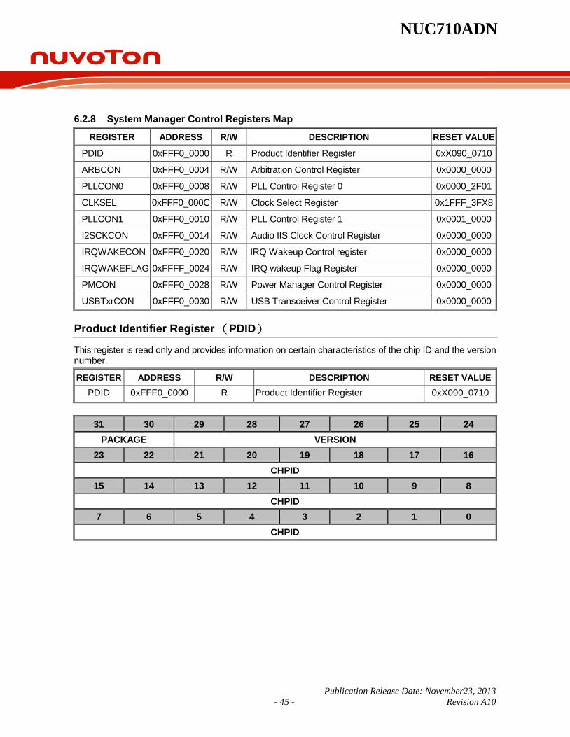
NUC710ADN
Publication Release Date: November23, 2013 - 45 - Revision A10
6.2.8 System Manager Control Registers Map
REGISTER ADDRESS R/W DESCRIPTION RESET VALUE
PDID 0xFFF0_0000 R Product Identifier Register 0xX090_0710
ARBCON 0xFFF0_0004 R/W Arbitration Control Register 0x0000_0000
PLLCON0 0xFFF0_0008 R/W PLL Control Register 0 0x0000_2F01
CLKSEL 0xFFF0_000C R/W Clock Select Register 0x1FFF_3FX8
PLLCON1 0xFFF0_0010 R/W PLL Control Register 1 0x0001_0000
I2SCKCON 0xFFF0_0014 R/W Audio IIS Clock Control Register 0x0000_0000
IRQWAKECON 0xFFF0_0020 R/W IRQ Wakeup Control register 0x0000_0000
IRQWAKEFLAG 0xFFFF_0024 R/W IRQ wakeup Flag Register 0x0000_0000
PMCON 0xFFF0_0028 R/W Power Manager Control Register 0x0000_0000
USBTxrCON 0xFFF0_0030 R/W USB Transceiver Control Register 0x0000_0000
Product Identifier Register (PDID)
This register is read only and provides information on certain characteristics of the chip ID and the version number.
REGISTER ADDRESS R/W DESCRIPTION RESET VALUE PDID 0xFFF0_0000 R Product Identifier Register 0xX090_0710
31 30 29 28 27 26 25 24 PACKAGE VERSION
23 22 21 20 19 18 17 16 CHPID
15 14 13 12 11 10 9 8 CHPID
7 6 5 4 3 2 1 0 CHPID

NUC710ADN
Publication Release Date: November235, 2013 - 46 - Revision A10
BITS DESCRIPTION
[31:30] PACKAGE
Package Type Select These two bits are power-on setting latched from pin D[9:8]
Package [31:30] Package Type 1 1 176-pin Package
[29:24] VERSION Version of chip [23:0] CHIPID The chip identifier 0x090.0710
Arbitration Control Register (ARBCON)
REGISTER ADDRESS R/W DESCRIPTION RESET VALUE ARBCON 0xFFF0_0004 R/W Arbitration Control Register 0x0000_0000
31 30 29 28 27 26 25 24
RESERVED 23 22 21 20 19 18 17 16
RESERVED 15 14 13 12 11 10 9 8
RESERVED 7 6 5 4 3 2 1 0
RESERVED IPACT IPEN PRTMOD
BITS DESCRIPTION [31:3] RESERVED -
[2] IPACT
Interrupt priority active. When IPEN=”1”, this bit will be set when the ARM core has an unmasked interrupt request. This bit is available only when the PRTMOD=0.
[1] IPEN
Interrupt priority enable bit 0 = the ARM core has the lowest priority. 1 = enable to raise the ARM core priority to second This bit is available only when the PRTMOD=0.
[0] PRTMOD Priority mode select 0 = Fixed Priority Mode (default) 1 = Rotate Priority Mode
PLL Control Register0 (PLLCON0)

NUC710ADN
Publication Release Date: November23, 2013 - 47 - Revision A10
NUC710 provides two clock signal generating options – crystal and oscillator. The external clock via EXTAL(15M) input pin as the reference clock input of the PLL module. The external clock can bypass the PLL and be used for the internal system clock by pulling down data pin D15. Using PLL’s output clock for the internal system clock, D15 must be pulled up.
REGISTER ADDRESS R/W DESCRIPTION RESET VALUE PLLCON 0xFFF0_0008 R/W PLL Control Register 0x0000_2F01
31 30 29 28 27 26 25 24
RESERVED
23 22 21 20 19 18 17 16
RESERVED PWDEN
15 14 13 12 11 10 9 8
FBDV
7 6 5 4 3 2 1 0
FBDV OTDV INDV
BITS DESCRIPTION [31:17] RESERVED -
[16] PWDEN Power down mode enable 0 = PLL is in normal mode (default) 1 = PLL is in power down mode
[15:7] FBDV PLL VCO output clock feedback divider Feedback Divider divides the output clock from VCO of PLL.
[6:5] OTDV
PLL output clock divider OTDV [6:5] DIVIDED BY
0 0 1 0 1 2 1 0 2 1 1 4
[4:0] INDV PLL input clock divider Input divider divides the input reference clock into the PLL.

NUC710ADN
Publication Release Date: November235, 2013 - 48 - Revision A10
Input Divider(NR)
PFD
FeedbackDivider
(NF)
ChargePump VCO
OutputDivider(NO)
ClockDivider
&Selector
EXTAL
ECLKS
OTDV[1:0] CLKS[2:0]
1
0
PLL
InternalSystemClock
INDV[4:0]
FBDV[8:0]
48MHzGen
480MHz
0
1
USBCKS
USBModule
FIN
FOUT
GP0
Fig 6.2.8.1 System PLL block diagram
PLL output clock formula:
FOUT = FIN NONR
NF 1∗∗
FOUT:Output clock of Output Divider FIN:External clock into the Input Divider NR:Input divider value (NR = INDV + 2) NF:Feedback divider value (NF = FBDV + 2) NO:Output divider value (NO = OTDV)
Clock Select Register (CLKSEL)
REGISTER ADDRESS R/W DESCRIPTION RESET VALUE CLKSEL 0xFFF0_000C R/W Clock Select Register 0x1FFF_7FX8
31 30 29 28 27 26 25 24
RESERVED PS2 KPI SCH1 SCH0 SSP 23 22 21 20 19 18 17 16
UART3 UART2 UART1 I2C1 I2C0 RTC PWM AC97 15 14 13 12 11 10 9 8
USBCKS USBD GDMA SD LCD EMC RESERVED WDT 7 6 5 4 3 2 1 0
USBH TIMER UART ECLKS CLKS RESET
BITS DESCRIPTION

NUC710ADN
Publication Release Date: November23, 2013 - 49 - Revision A10
[31:29] RESERVED -
[28] PS2 PS2 controller clock enable bit 0 = Disable PS2 controller clock 1 = Enable PS2 controller clock
[27] KPI Keypad controller clock enable bit 0 = Disable keypad controller clock 1 = Enable keypad controller clock
[26] SCH1 Smart Card Host controller 1 clock enable bit 0 = Disable smart card host controller 1 clock 1 = Enable smart card host controller 1 clock
[25] SCH0 Smart Card Host controller 0 clock enable bit 0 = Disable smart card host controller 0 clock 1 = Enable smart card host controller 0 clock
[24] USI USI controller clock enable bit 0 = Disable USI controller clock 1 = Enable USI controller clock
[23] UART3 UART3 controller clock enable bit 0 = Disable UART3 controller clock 1 = Enable UART3 controller clock
[22] UART2 UART2 controller clock enable bit 0 = Disable UART2 controller clock 1 = Enable UART2 controller clock
[21] UART1 UART1 controller clock enable bit 0 = Disable UART1 controller clock 1 = Enable UART1 controller clock
[20] I2C1 I2C1 controller clock enable bit 0 = Disable I2C1 controller clock 1 = Enable I2C1 controller clock
[19] I2C0 I2C0 controller clock enable bit 0 = Disable I2C0 controller clock 1 = Enable I2C0 controller clock
[18] RTC RTC unit clock enable bit 0 = Disable RTC controller clock 1 = Enable RTC controller clock
NUC710ADN
Publication Release Date: November235, 2013 - 50 - Revision A10
Continued.
BITS DESCRIPTION
[17] PWM PWM controller clock enable bit 0 = Disable PWM controller clock 1 = Enable PWM controller clock
[16] AC97 Audio Controller clock enable bit 0 = Disable AC97 controller clock 1 = Enable AC97 controller clock
[15] USBCKS
USB host/device 48MHz clock source Select bit 0 = USB clock 48MHz input from internal PLL (480MHz/10) 1 = USB clock 48MHz input from external GPIO0 pin. Pin direction must
be set to input.
[14] USBD USB device clock enable bit 0 = Disable USB device controller clock 1 = Enable USB device controller clock
[13] GDMA GDMA controller clock enable bit 0 = Disable GDMA clock 1 = Enable GDMA clock
[12] SD SD host controller clock enable bit 0 = Disable SD controller clock 1 = Enable SD controller clock
[11] LCD LCD controller clock enable bit 0 = Disable LCD controller clock 1 = Enable LCD controller clock
[10] EMC EMC controller clock enable bit 0 = Disable EMC controller clock 1 = Enable EMC controller clock
[9] RESERVED -
[8] WDT WDT clock enable bit 0 = Disable WDT counting clock 1 = Enable WDT counting clock
[7] USBH USB host clock enable bit 0 = Disable USB host controller clock 1 = Enable USB host controller clock
[6] TIMER Timer clock enable bit 0 = Disable timer clock 1 = Enable timer clock

NUC710ADN
Publication Release Date: November23, 2013 - 51 - Revision A10
Continued.
BITS DESCRIPTION
[5] UART0 UART0 controller clock enable bit 0 = Disable UART0 controller clock 1 = Enable UART0 controller clock
[4] ECLKS
External clock select 0 = External clock from EXTAL pin is used as system clock 1 = PLL output clock is used as system clock After power on reset, the content of ECLKS is the Power-On Setting value. You can program this bit to change the system clock source.
[3:1] CLKS
PLL output clock select CLKS [3:1] System clock
0 0 0 58.594 KHz* 0 0 1 24 MHz 0 1 0 48 MHz 0 1 1 60 MHz 1 0 0 80 MHz 1 0 1 RESERVED 1 1 0 RESERVED 1 1 1 RESERVED
Note: 1. These values are based on PLL output(FOUT) is 480MHz. 2. When 24Mhz ~ 80MHz is selected, the ECLKS bit must be set to 1. 3. About 58.594KHz setting, two steps are needed. First, clear ECLKS
bit, and then clear CLKS.
[0] RESET Software reset bit Set the software reset control bit to 1 to generate an internal reset pulse. This bit automatically clears to logic 0 after the reset pulse.

NUC710ADN
Publication Release Date: November235, 2013 - 52 - Revision A10
PLL Control Register 1(PLLCON1)
NUC710 provides extra a PLL for the LCD controller programmable pixel clock and provides 12.288/16.934 MHz clock source to Audio Controller. It uses the same 15MHz crystal clock input source with the system PLL mentioned above.
REGISTER ADDRESS R/W DESCRIPTION RESET VALUE PLLCON1 0xFFF0_0010 R/W PLL Control Register 1 0x0001_0000
31 30 29 28 27 26 25 24
RESERVED
23 22 21 20 19 18 17 16
RESERVED PWDEN1
15 14 13 12 11 10 9 8
FBDV1
7 6 5 4 3 2 1 0
FBDV1 OTDV1 INDV1
BITS DESCRIPTION
[31:17] RESERVED -
[16] PWDEN1 PLL1 power down enable 0 = PLL1 is in normal mode 1 = PLL1 is in power down mode (default)
[15:7] FBDV1 PLL1 VCO output clock feedback divider Feedback Divider divides the output clock from VCO of PLL1.
[6:5] OTDV1
PLL1 output clock divider OTDV1 [6:5] Divided by 0 0 1 0 1 2 1 0 2 1 1 4
[4:0] INDV1 PLL1 input clock divider Input divider divides the input reference clock into the PLL1.

NUC710ADN
Publication Release Date: November23, 2013 - 53 - Revision A10
Input Divider(NR)
PFD
FeedbackDivider
(NF)
ChargePump VCO
OutputDivider(NO)
EXTAL
OTDV1[1:0]
PLL1INDV1[4:0]
FBDV1[8:0]
480MHz
FIN
FOUT
to LCD controller
to Audio Controller
Fig 6.2.8.2 LCD PLL block diagram
PLL output clock formula is:
FOUT = FIN NONR
NF 1∗∗
FOUT:Output clock of Output Divider
FIN:External clock into the Input Divider NR:Input divider value (NR = INDV1 + 2) NF:Feedback divider value (NF = FBDV1 + 2) NO:Output divider value (NO = OTDV1)
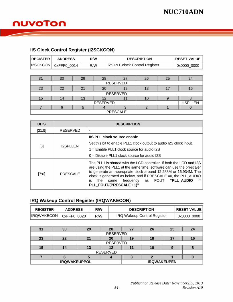
NUC710ADN
Publication Release Date: November235, 2013 - 54 - Revision A10
IIS Clock Control Register (I2SCKCON)
REGISTER ADDRESS R/W DESCRIPTION RESET VALUE I2SCKCON 0xFFF0_0014 R/W I2S PLL clock Control Register 0x0000_0000
31 30 29 28 27 26 25 24
RESERVED 23 22 21 20 19 18 17 16
RESERVED 15 14 13 12 11 10 9 8
RESERVED IISPLLEN 7 6 5 4 3 2 1 0
PRESCALE
BITS DESCRIPTION
[31:9] RESERVED -
[8] I2SPLLEN
IIS PLL clock source enable Set this bit to enable PLL1 clock output to audio I2S clock input. 1 = Enable PLL1 clock source for audio I2S 0 = Disable PLL1 clock source for audio I2S
[7:0] PRESCALE
The PLL1 is shared with the LCD controller. If both the LCD and I2S are using the PLL1 at the same time, software can use the prescaler to generate an appropriate clock around 12.288M or 16.934M. The clock is generated as below, and if PRESCALE =0, the PLL_AUDIO is the same frequency as FOUT “PLL_AUDIO = PLL_FOUT/(PRESCALE +1)”
IRQ Wakeup Control Register (IRQWAKECON)
REGISTER ADDRESS R/W DESCRIPTION RESET VALUE IRQWAKECON 0xFFF0_0020 R/W IRQ Wakeup Control Register 0x0000_0000
31 30 29 28 27 26 25 24
RESERVED 23 22 21 20 19 18 17 16
RESERVED 15 14 13 12 11 10 9 8
RESERVED 7 6 5 4 3 2 1 0
IRQWAKEUPPOL IRQWAKEUPEN

NUC710ADN
Publication Release Date: November23, 2013 - 55 - Revision A10
BITS DESCRIPTION
[31:8] RESERVED
[7] IRQWAKEUPPOL[3] nIRQ3 wake up polarity 1 = nIRQ3 is high level wake up 0 = nIRQ3 is low level wake up
[6] IRQWAKEUPPOL[2] nIRQ2 wake up polarity 1 = nIRQ2 is high level wake up 0 = nIRQ2 is low level wake up
[5] IRQWAKEUPPOL[1] nIRQ1 wake up polarity 1 = nIRQ1 is high level wake up 0 = nIRQ1 is low level wake up
[4] IRQWAKEUPPOL[0] nIRQ0 wake up polarity 1 = nIRQ0 is high level wake up 0 = nIRQ0 is low level wake up
[3] IRQWAKEUPEN[3] nIRQ3 wake up enable bit 1 = nIRQ3 wake up enable 0 = nIRQ3 wake up disable
[2] IRQWAKEUPEN[2] nIRQ2 wake up enable bit 1 = nIRQ2 wake up enable 0 = nIRQ2 wake up disable
[1] IRQWAKEUPEN[1] nIRQ1 wake up enable bit 1 = nIRQ1 wake up enable 0 = nIRQ1 wake up disable
[0] IRQWAKEUPEN[0] nIRQ0 wake up enable bit 1 = nIRQ0 wake up enable 0 = nIRQ0 wake up disable
IRQ Wakeup Flag Register (IRQWAKEFLAG)
REGISTER ADDRESS R/W DESCRIPTION RESET VALUE IRQWAKEFLAG 0xFFF0_0024 R/W IRQ Wakeup Flag Register 0x0000_0000

NUC710ADN
Publication Release Date: November235, 2013 - 56 - Revision A10
31 30 29 28 27 26 25 24
RESERVED 23 22 21 20 19 18 17 16
RESERVED 15 14 13 12 11 10 9 8
RESERVED 7 6 5 4 3 2 1 0
RESERVED IRQWAKEFLAG This register is used to record the wakeup events, after clock recovery, software should check these flags to identify which nIRQ is used to wakeup the system. And clear the flags in an IRQ interrupt service routine.
BITS DESCRIPTION [31:4] RESERVED -
[3] IRQWAKEFLAG[3] nIRQ3 wake up flag 1 = Chip is woken up by nIRQ3 0 = No active
[2] IRQWAKEFLAG[2] nIRQ2 wake up flag 1 = Chip is woken up by nIRQ2 0 = No active
[1] IRQWAKEFLAG[1] nIRQ1 wake up flag 1 = Chip is woken up by nIRQ1 0 = No active
[0] IRQWAKEFLAG[0] nIRQ0 wake up flag 1 = Chip is woken up by nIRQ0 0 = No active
Power Management Control Register (PMCON)
REGISTER ADDRESS R/W DESCRIPTION RESET VALUE PMCON 0xFFF0_0028 R/W Power Management Control Register 0x0000_0000
31 30 29 28 27 26 25 24 PUP_DIS RESERVED
23 22 21 20 19 18 17 16 RESERVED
15 14 13 12 11 10 9 8 RESERVED
7 6 5 4 3 2 1 0 RESERVED MIDLE PD IDLE
BITS DESCRIPTION
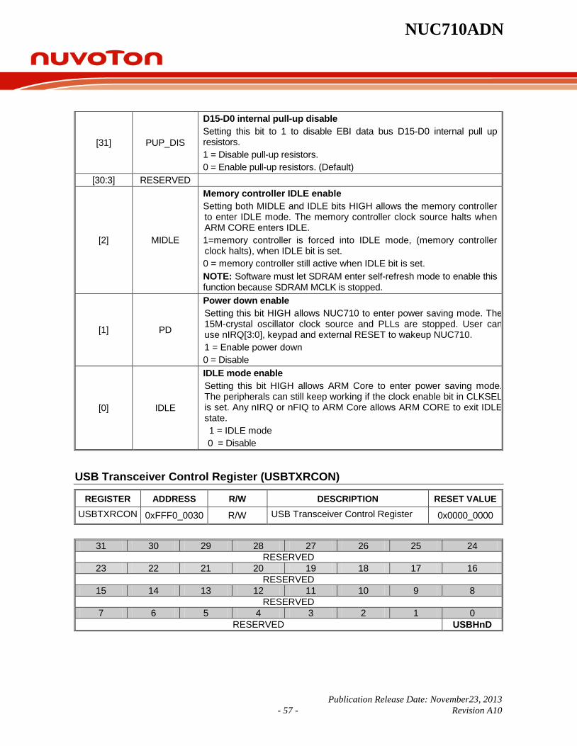
NUC710ADN
Publication Release Date: November23, 2013 - 57 - Revision A10
[31] PUP_DIS
D15-D0 internal pull-up disable Setting this bit to 1 to disable EBI data bus D15-D0 internal pull up resistors. 1 = Disable pull-up resistors. 0 = Enable pull-up resistors. (Default)
[30:3] RESERVED
[2] MIDLE
Memory controller IDLE enable Setting both MIDLE and IDLE bits HIGH allows the memory controller to enter IDLE mode. The memory controller clock source halts when ARM CORE enters IDLE. 1=memory controller is forced into IDLE mode, (memory controller clock halts), when IDLE bit is set. 0 = memory controller still active when IDLE bit is set. NOTE: Software must let SDRAM enter self-refresh mode to enable this function because SDRAM MCLK is stopped.
[1] PD
Power down enable Setting this bit HIGH allows NUC710 to enter power saving mode. The 15M-crystal oscillator clock source and PLLs are stopped. User can use nIRQ[3:0], keypad and external RESET to wakeup NUC710. 1 = Enable power down 0 = Disable
[0] IDLE
IDLE mode enable Setting this bit HIGH allows ARM Core to enter power saving mode. The peripherals can still keep working if the clock enable bit in CLKSEL is set. Any nIRQ or nFIQ to ARM Core allows ARM CORE to exit IDLE state. 1 = IDLE mode 0 = Disable
USB Transceiver Control Register (USBTXRCON)
REGISTER ADDRESS R/W DESCRIPTION RESET VALUE USBTXRCON 0xFFF0_0030 R/W USB Transceiver Control Register 0x0000_0000
31 30 29 28 27 26 25 24 RESERVED
23 22 21 20 19 18 17 16 RESERVED
15 14 13 12 11 10 9 8 RESERVED
7 6 5 4 3 2 1 0 RESERVED USBHnD
NUC710ADN
Publication Release Date: November235, 2013 - 58 - Revision A10
BITS DESCRIPTION
[31:1] RESERVED -
[0] USBHnD
USBHnD[0]: USB transceiver control
There are two USB1.1 built-in transceivers. One is a dedicated USB host, and the other is shared with USB device. This bit can be set in software to toggle the transceiver path. 1 = HOST 0 = Device
6.3 External Bus Interface 6.3.1 EBI Overview NUC710 supports External Bus Interface (EBI), which controls access to external memory (ROM/FLASH, SDRAM) and External I/O devices. The EBI has seven chip selects to select one ROM/FLASH bank, two SDRAM banks, and four External I/O banks. The address bus is 22-bits. It supports an 8-bit, 16-bit, and 32-bit external data bus width for each bank. The EBI has the following functions: SDRAM controller EBI control register ROM/FLASH interface External I/O interface External bus mastership
6.3.2 SDRAM Controller The SDRAM controller module within NUC710 contains configuration registers, timing control registers, the common control register, and other logic to provide an 8, 16, and 32-bit SDRAM interface with a single 8, 16, 32-bit SDRAM device or two 8-bit devices wired to provide a 16-bit data path or two 16-bit devices wired to give a 32-bit data path. The maximum size of each bank is 64M bytes, and maximum memory size can span up to 128MB. The SDRAM controller has the following features: Supports up to 2 external SDRAM banks Maximum size of each bank is 64M bytes 8, 16, 32-bit data interface Programmable CAS Latency: 1, 2 and 3 Fixed Burst Length: 1 Sequential burst type Auto Refresh Mode and Self Refresh Mode Adjustable Refresh Rate Power up sequence
6.3.2.1 SDRAM Components Supported

NUC710ADN
Publication Release Date: November23, 2013 - 59 - Revision A10
Table 6.3.2.1 SDRAM supported by NUC710 SIZE TYPE BANKS ROW ADDRESSING COLUMN ADDRESSING
16M bits 2Mx8 2 RA0~RA10 CA0~CA8 1Mx16 2 RA0~RA10 CA0~CA7
64M bits 8Mx8 4 RA0~RA11 CA0~CA8 4Mx16 4 RA0~RA11 CA0~CA7 2Mx32 4 RA0~RA10 CA0~CA7
128M bits 16Mx8 4 RA0~RA11 CA0~CA9
8Mx16 4 RA0~RA11 CA0~CA8 4Mx32 4 RA0~RA11 CA0~CA7
256M bits 32Mx8 4 RA0~RA12 CA0~CA9 16Mx16 4 RA0~RA12 CA0~CA8
AHB Bus Address Mapping to SDRAM Bus Note: * indicates the signal is not used; ** indicates the signal is fixed at logic 0 and is not used;
The HADDR prefixes have been omitted on the following tables. A14 ~ A0 are the Address pins of the NUC710 EBI interface; A14 and A13 are the Bank Select Signals of SDRAM.
SDRAM Data Bus Width: 32-bit
Total Type R x C R/C A14
(BS1) A13
(BS0) A12 A11 A10 A9 A8 A7 A6 A5 A4 A3 A2 A1 A0
16M 2Mx8 11x9 R ** 11 ** 11* 22 21 20 19 18 17 16 15 14 13 12 C ** 11 ** 11* AP 25* 10 9 8 7 6 5 4 3 2
16M 1Mx16 11x8 R ** 10 ** 10* 11 21 20 19 18 17 16 15 14 13 12 C ** 10 ** 10* AP 25* 10* 9 8 7 6 5 4 3 2
64M 8Mx8 12x9 R 11 12 11* 23 22 21 20 19 18 17 16 15 14 13 24 C 11 12 11* 23* AP 25* 10 9 8 7 6 5 4 3 2
64M 4Mx16 12x8 R 11 10 11* 23 22 21 20 19 18 17 16 15 14 13 12 C 11 10 11* 23* AP 25* 24* 9 8 7 6 5 4 3 2
64M 2Mx32 11x8 R 11 10 11* 23* 22 21 20 19 18 17 16 15 14 13 12 C 11 10 11* 23* AP 25* 24* 9 8 7 6 5 4 3 2
128M* 16Mx8 12x10 R 11 12 11* 23 22 21 20 19 18 17 16 15 14 13 24 C 11 12 11* 23* AP 25 10 9 8 7 6 5 4 3 2
128M 8Mx16 12x9 R 11 12 11* 23 22 21 20 19 18 17 16 15 14 13 24 C 11 12 11* 23* AP 25* 10 9 8 7 6 5 4 3 2
128M 4Mx32 12x8 R 11 10 11* 23 22 21 20 19 18 17 16 15 14 13 12 C 11 10 11* 23* AP 25* 10* 9 8 7 6 5 4 3 2
256M* 32Mx8 13x10 R 11 12 24 23 22 21 20 19 18 17 16 15 14 13 25 C 11 12 24* 23* AP 26* 10 9 8 7 6 5 4 3 2
256M* 16Mx16 13x9 R 11 12 24 23 22 21 20 19 18 17 16 15 14 13 25 C 11 12 24* 23* AP 26* 10* 9 8 7 6 5 4 3 2

NUC710ADN
Publication Release Date: November235, 2013 - 60 - Revision A10
SDRAM Data Bus Width: 16-bit
Total Type R x C R/C A14
(BS1) A13
(BS0) A12 A11 A10 A9 A8 A7 A6 A5 A4 A3 A2 A1 A0
16M 2Mx8 11x9 R ** 10 ** 10* 21 20 19 18 17 16 15 14 13 12 11
C ** 10 ** 10* AP 24* 9 8 7 6 5 4 3 2 1
16M 1Mx16 11x8 R ** 9 ** 9* 10 20 19 18 17 16 15 14 13 12 11
C ** 9 ** 9* AP 24* 9* 8 7 6 5 4 3 2 1
64M 8Mx8 12x9 R 10 11 10* 22 21 20 19 18 17 16 15 14 13 12 23
C 10 11 10* 22* AP 24* 9 8 7 6 5 4 3 2 1
64M 4Mx16 12x8 R 10 9 10* 22 21 20 19 18 17 16 15 14 13 12 11
C 10 9 10* 22* AP 24* 23* 8 7 6 5 4 3 2 1
64M 2Mx32 11x8 R 10 9 10* 22* 21 20 19 18 17 16 15 14 13 12 11
C 10 9 10* 22* AP 24* 23* 8 7 6 5 4 3 2 1
128M 16Mx8 12x10 R 10 11 10* 22 21 20 19 18 17 16 15 14 13 12 23
C 10 11 10* 22* AP 24 9 8 7 6 5 4 3 2 1
128M 8Mx16 12x9 R 10 11 10* 22 21 20 19 18 17 16 15 14 13 12 23
C 10 11 10* 22* AP 24* 9 8 7 6 5 4 3 2 1
128M 4Mx32 12x8 R 10 9 10* 22 21 20 19 18 17 16 15 14 13 12 11
C 10 9 10* 22* AP 24* 9* 8 7 6 5 4 3 2 1
256M* 32Mx8 13x10 R 10 11 23 22 21 20 19 18 17 16 15 14 13 12 24
C 10 11 23* 22* AP 25* 9 8 7 6 5 4 3 2 1
256M 16Mx16 13x9 R 10 11 23 22 21 20 19 18 17 16 15 14 13 12 24
C 10 11 23* 22* AP 25* 9 8 7 6 5 4 3 2 1

NUC710ADN
Publication Release Date: November23, 2013 - 61 - Revision A10
SDRAM Data Bus Width: 8-bit
Total Type R x C R/C A14
(BS1) A13
(BS0) A12 A11 A10 A9 A8 A7 A6 A5 A4 A3 A2 A1 A0
16M 2Mx8 11x9 R ** 9 ** 9* 20 19 18 17 16 15 14 13 12 11 10
C ** 9 ** 9* AP 23* 8 7 6 5 4 3 2 1 0
16M 1Mx16 11x8 R ** 8 ** 8* 9 19 18 17 16 15 14 13 12 11 10
C ** 8 ** 8* AP 23* 8* 7 6 5 4 3 2 1 0
64M 8Mx8 12x9 R 9 10 9* 21 20 19 18 17 16 15 14 13 12 11 22
C 9 10 9* 21* AP 23* 8 7 6 5 4 3 2 1 1
64M 4Mx16 12x8 R 9 8 9* 21 20 19 18 17 16 15 14 13 12 11 10
C 9 8 9* 21* AP 23* 22* 7 6 5 4 3 2 1 0
64M 2Mx32 11x8 R 9 8 9* 21* 20 19 18 17 16 15 14 13 12 11 10
C 9 8 9* 21* AP 23* 22* 7 6 5 4 3 2 1 0
128M 16Mx8 12x10 R 9 10 9* 21 20 19 18 17 16 15 14 13 12 11 22
C 9 10 9* 21* AP 23 8 7 6 5 4 3 2 1 0
128M 8Mx16 12x9 R 9 10 9* 21 20 19 18 17 16 15 14 13 12 11 22
C 9 10 9* 21* AP 23* 8 7 6 5 4 3 2 1 0
128M 4Mx32 12x8 R 9 8 9* 21 20 19 18 17 16 15 14 13 12 11 10
C 9 8 9* 21* AP 23* 8* 7 6 5 4 3 2 1 0
256M 32Mx8 13x10 R 9 10 22 21 20 19 18 17 16 15 14 13 12 11 23
C 9 10 22* 21* AP 24 8 7 6 5 4 3 2 1 0
256M 16Mx16 13x9 R 9 10 22 21 20 19 18 17 16 15 14 13 12 11 23
C 9 10 22* 21* AP 24* 8 7 6 5 4 3 2 1 0
6.3.2.2 SDRAM Power Up Sequence SDRAM must be initialized after power-on. NUC710 SDRAM Controller automatically executes initialization and sets the mode register of each bank to default values. The default values are:
— Burst Length = 1 — Burst Type = Sequential (fixed) — CAS Latency = 2 — Write Burst Length = Burst (fixed)
The value of mode register can be changed after the power-on sequence by setting the value of the corresponding bank’s configuration register “LENGTH” and “LATENCY” bits and set the MRSET bit enable to execute the Mode Register Set command.

NUC710ADN
Publication Release Date: November235, 2013 - 62 - Revision A10
6.3.2.3 SDRAM Interface
MCLK
MCKE
nSCS[1:0]
nSRAS
nSCAS
nSWE
nSDQM[3:0]
A[21:0]
D[31:0]
A[10:0]
DQ[[31:0]
DQM[3:0]
nWE
nCAS
nRAS
nCS
BS0
BS1
CLK
CKE
W90P710
A13
A14
A[10:0]
nSCS0
SDRAM64Mb 512Kx4x32
nSDQM[3:0]
Fig 6.3.1 SDRAM Interface
6.3.3 EBI Control Registers Map
REGISTER ADDRESS R/W DESCRIPTION RESET VALUE EBICON 0xFFF0_1000 R/W EBI control register 0x0001_0000
ROMCON 0xFFF0_1004 R/W ROM/FLASH control register 0x0000_0XFC
SDCONF0 0xFFF0_1008 R/W SDRAM bank 0 configuration register 0x0000_0800 SDCONF1 0xFFF0_100C R/W SDRAM bank 1 configuration register 0x0000_0800 SDTIME0 0xFFF0_1010 R/W SDRAM bank 0 timing control register 0x0000_0000 SDTIME1 0xFFF0_1014 R/W SDRAM bank 1 timing control register 0x0000_0000 EXT0CON 0xFFF0_1018 R/W External I/O 0 control register 0x0000_0000
EXT1CON 0xFFF0_101C R/W External I/O 1 control register 0x0000_0000
EXT2CON 0xFFF0_1020 R/W External I/O 2 control register 0x0000_0000
EXT3CON 0xFFF0_1024 R/W External I/O 3 control register 0x0000_0000
CKSKEW 0xFFF0_1F00 R/W Clock skew control register (for testing) 0xXXXX_0038
EBI Control Register (EBICON)

NUC710ADN
Publication Release Date: November23, 2013 - 63 - Revision A10
REGISTER ADDRESS R/W DESCRIPTION RESET VALUE EBICON 0xFFF0_1000 R/W EBI control register 0x0001_0000
31 30 29 28 27 26 25 24
RESERVED EXBE3 EXBE2 EXBE1 EXBE0
23 22 21 20 19 18 17 16
RESERVED REFEN REFMOD CLKEN
15 14 13 12 11 10 9 8
REFRAT
7 6 5 4 3 2 1 0
REFRAT WAITVT LITTLE
BITS DESCRIPTION
[31:28] RESERVED
[27] EXBE3
External IO bank 3 byte enable This function is used for some devices that with high and low bytes enable signals to control which byte will be written or masked data output when read. For this kind device, software can set this bit HIGH to implement this function. Detail pin interconnection is showed as Fig6.3.8. 1 = nWBE[3:0] pin is byte enable signals, nWE will be used as write
strobe signal to SRAM. 0 = nWBE[3:0] pin is byte write strobe signal.
[26] EXBE2
External IO bank 2 byte enable The bit function description is the same as EXBE3 above. 1 = nWBE[3:0] pin is byte enable signals, nWE will be used as write
strobe signal to SRAM. 0 = nWBE[3:0] pin is byte write strobe signal.
[25] EXBE1
External IO bank 1 byte enable The bit function description is the same as EXBE3 above. 1 = nWBE[3:0] pin is byte enable signals, nWE will be used as write
strobe signal to SRAM 0 = nWBE[3:0] pin is byte write strobe signal

NUC710ADN
Publication Release Date: November235, 2013 - 64 - Revision A10
Continued.
BITS DESCRIPTION
[24] EXBE0
External IO bank 0 byte enable The function description for this bit is the same as EXBE3 above. 1 = nWBE[3:0] pin is byte enable signals, nWE will be used as write
strobe signal to SRAM 0 = nWBE[3:0] pin is byte write strobe signal
[23:19] RESERVED
[18] REFEN
Enable SDRAM refresh cycle for SDRAM bank0 & bank1 Set this bit to start the SDRAM auto-refresh cycle. The refresh rate is according to the REFRAT bits. 1 = Enable refresh function 0 = Disable refresh function
[17] REFMOD
Refresh mode of SDRAM for SDRAM bank Defines the refresh mode type of external SDRAM bank Software can write this bit “1” to force SDRAM enter self-refresh mode. 0 = Auto refresh mode 1 = Self refresh mode NOTE: If any read/write to SDRAM occurs then this bit will be automatically cleared to “0” by hardware, and SDRAM will enter auto-refresh mode.
[16] CLKEN
Clock enable for SDRAM Enables the SDRAM clock enable (CKE) control signal 0 = Disable (power down mode) 1 = Enable (Default)
[15:3] REFRAT
Refresh count value for SDRAM The SDRAM Controller provides an auto-refresh cycle for every refresh period stored in the REFRAT bits when the REFEN bit of each bank is set.
The refresh period is calculated as fMCLKvalueperiod =

NUC710ADN
Publication Release Date: November23, 2013 - 65 - Revision A10
Continued.
BITS DESCRIPTION
[2:1] WAITVT
Valid time of nWAIT signal NUC710 recognizes the nWAIT signal at the “nth” MCLK positive edge after the nOE or nWBE active cycle. WAITVT bits determine n.
WAITVT [2:1] nth MCLK 0 0 1 0 1 2 1 0 3 1 1 4
[0] LITTLE
Little-endian mode After power on reset, the content of LITTLE is the Power-On Setting value from D14 pin. If pin D14 is pulled down, the external memory format is Big-endian mode. If pin D14 is pulled up, the external memory format is Little-endian mode. For more details, refer to Power-On Setting of System Manager. NOTE: This bit is read only.
ROM/Flash Control Register (ROMCON)
REGISTER ADDRESS R/W DESCRIPTION RESET VALUE ROMCON 0xFFF0_1004 R/W ROM/FLASH control register 0x0000_0XFC
31 30 29 28 27 26 25 24
BASADDR
23 22 21 20 19 18 17 16
BASADDR SIZE
15 14 13 12 11 10 9 8
RESERVED tPA
7 6 5 4 3 2 1 0
tACC BTSIZE PGMODE

NUC710ADN
Publication Release Date: November235, 2013 - 66 - Revision A10
BITS DESCRIPTION
[31:19] BASADDR
Base address pointer of ROM/Flash bank The start address is calculated as ROM/Flash bank base pointer << 18. The base address pointer together with the “SIZE” bits constitutes the whole address range of each bank.
[18:16] SIZE
The size of ROM/FLASH memory SIZE [10:8] Byte
0 0 0 256K 0 0 1 512K 0 1 0 1M 0 1 1 2M 1 0 0 4M 1 0 1 8M 1 1 0 16M 1 1 1 RESERVED
[15:12] RESERVED -
[11:8] tPA
Page mode access cycle time tPA[11:8] MCLK tPA[11:8] MCLK
0 0 0 0 1 1 0 0 0 10 0 0 0 1 2 1 0 0 1 12 0 0 1 0 3 1 0 1 0 14 0 0 1 1 4 1 0 1 1 16 0 1 0 0 5 1 1 0 0 18 0 1 0 1 6 1 1 0 1 20 0 1 1 0 7 1 1 1 0 22 0 1 1 1 8 1 1 1 1 24
[7:4] tACC
Access cycle time tACC[11:8] MCLK tACC[11:8] MCLK
0 0 0 0 1 1 0 0 0 10 0 0 0 1 2 1 0 0 1 12 0 0 1 0 3 1 0 1 0 14 0 0 1 1 4 1 0 1 1 16 0 1 0 0 5 1 1 0 0 18 0 1 0 1 6 1 1 0 1 20 0 1 1 0 7 1 1 1 0 22 0 1 1 1 8 1 1 1 1 24
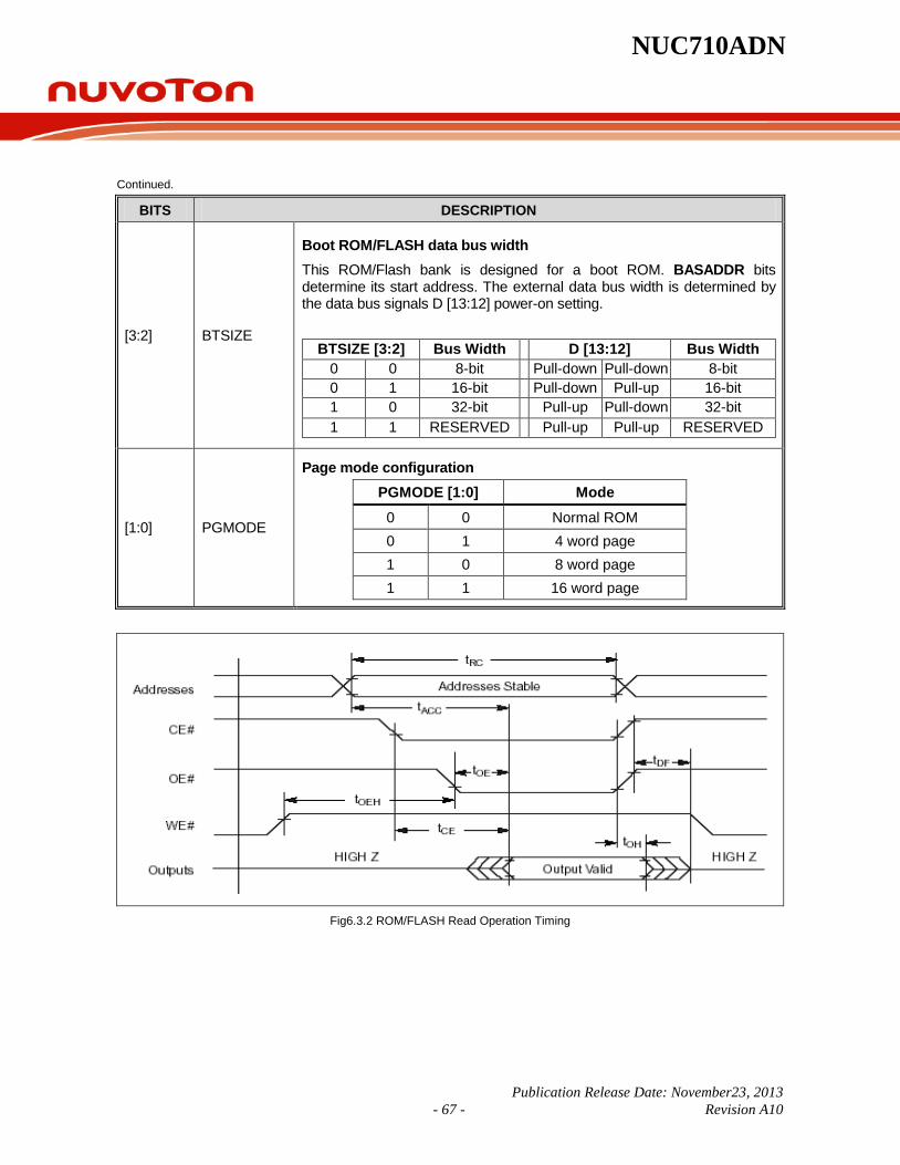
NUC710ADN
Publication Release Date: November23, 2013 - 67 - Revision A10
Continued.
BITS DESCRIPTION
[3:2] BTSIZE
Boot ROM/FLASH data bus width This ROM/Flash bank is designed for a boot ROM. BASADDR bits determine its start address. The external data bus width is determined by the data bus signals D [13:12] power-on setting.
BTSIZE [3:2] Bus Width D [13:12] Bus Width 0 0 8-bit Pull-down Pull-down 8-bit 0 1 16-bit Pull-down Pull-up 16-bit 1 0 32-bit Pull-up Pull-down 32-bit 1 1 RESERVED Pull-up Pull-up RESERVED
[1:0] PGMODE
Page mode configuration PGMODE [1:0] Mode
0 0 Normal ROM 0 1 4 word page 1 0 8 word page 1 1 16 word page
Fig6.3.2 ROM/FLASH Read Operation Timing
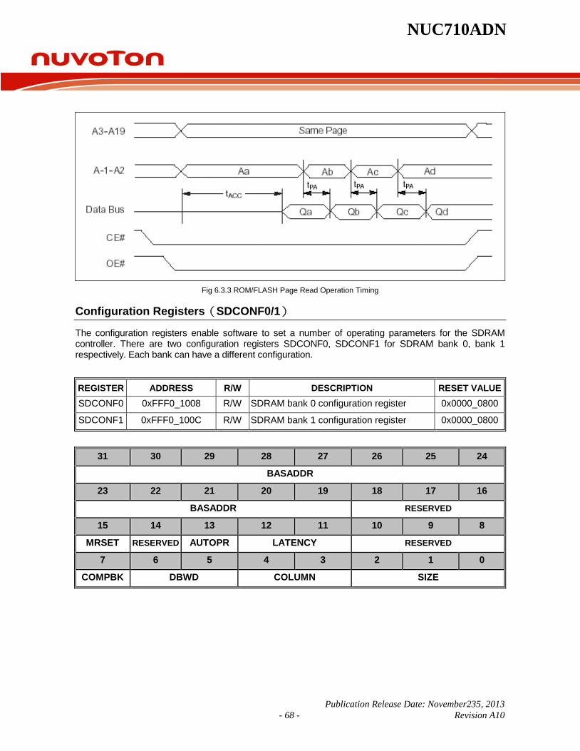
NUC710ADN
Publication Release Date: November235, 2013 - 68 - Revision A10
Fig 6.3.3 ROM/FLASH Page Read Operation Timing
Configuration Registers(SDCONF0/1)
The configuration registers enable software to set a number of operating parameters for the SDRAM controller. There are two configuration registers SDCONF0, SDCONF1 for SDRAM bank 0, bank 1 respectively. Each bank can have a different configuration.
REGISTER ADDRESS R/W DESCRIPTION RESET VALUE SDCONF0 0xFFF0_1008 R/W SDRAM bank 0 configuration register 0x0000_0800
SDCONF1 0xFFF0_100C R/W SDRAM bank 1 configuration register 0x0000_0800
31 30 29 28 27 26 25 24
BASADDR
23 22 21 20 19 18 17 16
BASADDR RESERVED
15 14 13 12 11 10 9 8
MRSET RESERVED AUTOPR LATENCY RESERVED
7 6 5 4 3 2 1 0
COMPBK DBWD COLUMN SIZE

NUC710ADN
Publication Release Date: November23, 2013 - 69 - Revision A10
BITS DESCRIPTION
[31:19] BASADDR
Base address pointer of SDRAM bank 0/1 The start address is calculated as SDRAM bank 0/1 base pointer << 18. The SDRAM base address pointer together with the “SIZE” bits constitutes the whole address range of each SDRAM bank.
[18:16] RESERVED -
[15] MRSET SDRAM Mode register set command for SDRAM bank 0/1 Set this bit to issue a mode register set command to SDRAM.
[14] RESERVED -
[13] AUTOPR
SDRAM bank 0/1 auto precharge mode Enable the auto precharge function of external SDRAM bank 0/1 1= Auto precharge 0 = No auto precharge
[12:11] LATENCY
The CAS Latency of SDRAM bank 0/1 Defines the CAS latency of external SDRAM bank 0/1
LATENCY [12:11] MCLK 0 0 1 0 1 2 1 0 3 1 1 REVERSED
[10:8] RESERVED -
[7] COMPBK
Number of component bank in SDRAM bank 0/1 Indicates the number of component bank (2 or 4 banks) in external SDRAM bank 0/1. 0 = 2 banks 1 = 4 banks
[6:5] DBWD
Data bus width for SDRAM bank 0/1 Indicates the external data bus width connect with SDRAM bank 0/1 If DBWD = 00, the assigned SDRAM access signal is not generated i.e. disable.
DBWD [6:5] Bits 0 0 Bank disable 0 1 8-bit (byte) 1 0 16-bit (half-word) 1 1 32-bit (word)
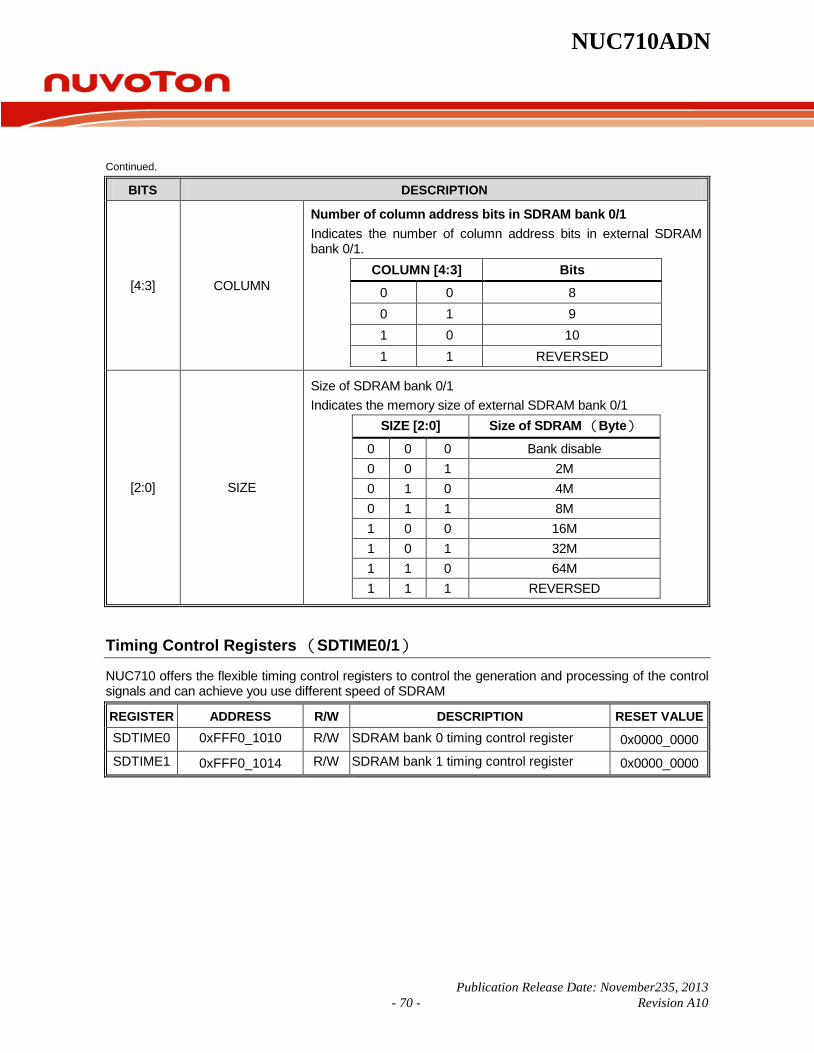
NUC710ADN
Publication Release Date: November235, 2013 - 70 - Revision A10
Continued.
BITS DESCRIPTION
[4:3] COLUMN
Number of column address bits in SDRAM bank 0/1 Indicates the number of column address bits in external SDRAM bank 0/1.
COLUMN [4:3] Bits 0 0 8 0 1 9 1 0 10 1 1 REVERSED
[2:0] SIZE
Size of SDRAM bank 0/1 Indicates the memory size of external SDRAM bank 0/1
SIZE [2:0] Size of SDRAM (Byte)
0 0 0 Bank disable 0 0 1 2M 0 1 0 4M 0 1 1 8M 1 0 0 16M 1 0 1 32M 1 1 0 64M 1 1 1 REVERSED
Timing Control Registers (SDTIME0/1)
NUC710 offers the flexible timing control registers to control the generation and processing of the control signals and can achieve you use different speed of SDRAM
REGISTER ADDRESS R/W DESCRIPTION RESET VALUE SDTIME0 0xFFF0_1010 R/W SDRAM bank 0 timing control register 0x0000_0000 SDTIME1 0xFFF0_1014 R/W SDRAM bank 1 timing control register 0x0000_0000
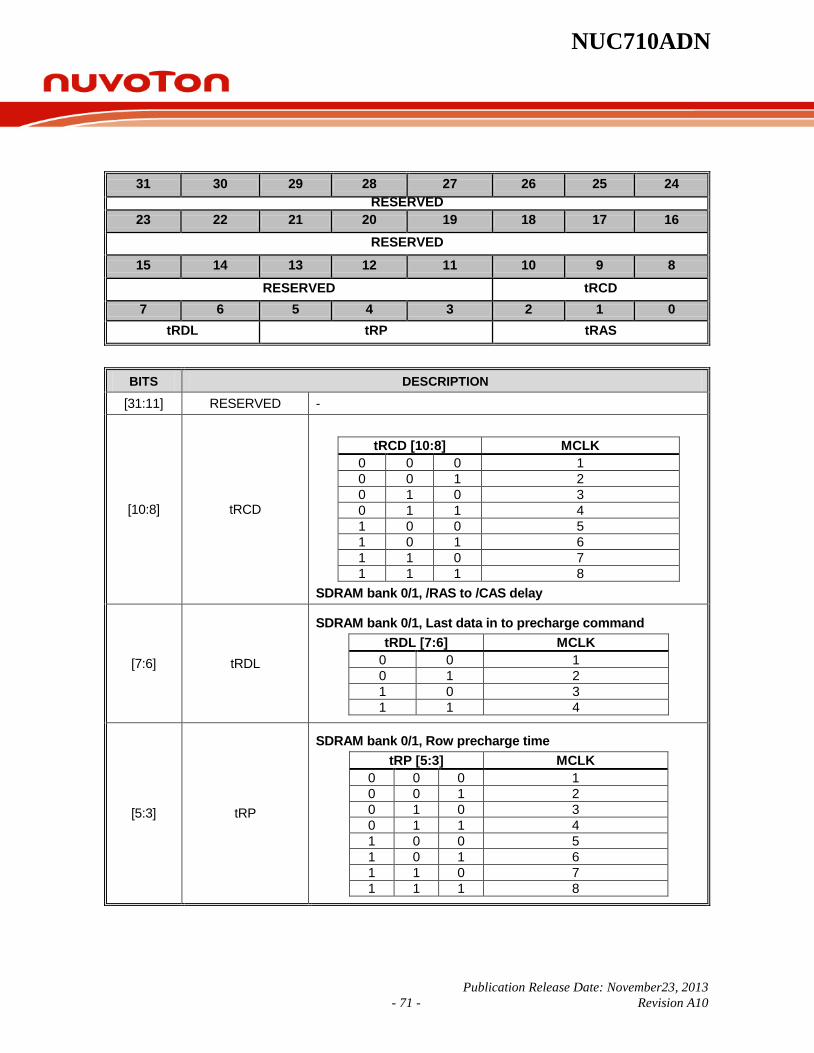
NUC710ADN
Publication Release Date: November23, 2013 - 71 - Revision A10
31 30 29 28 27 26 25 24 RESERVED
23 22 21 20 19 18 17 16 RESERVED
15 14 13 12 11 10 9 8 RESERVED tRCD
7 6 5 4 3 2 1 0 tRDL tRP tRAS
BITS DESCRIPTION
[31:11] RESERVED -
[10:8] tRCD
SDRAM bank 0/1, /RAS to /CAS delay
tRCD [10:8] MCLK 0 0 0 1 0 0 1 2 0 1 0 3 0 1 1 4 1 0 0 5 1 0 1 6 1 1 0 7 1 1 1 8
[7:6] tRDL
SDRAM bank 0/1, Last data in to precharge command tRDL [7:6] MCLK
0 0 1 0 1 2 1 0 3 1 1 4
[5:3] tRP
SDRAM bank 0/1, Row precharge time tRP [5:3] MCLK
0 0 0 1 0 0 1 2 0 1 0 3 0 1 1 4 1 0 0 5 1 0 1 6 1 1 0 7 1 1 1 8

NUC710ADN
Publication Release Date: November235, 2013 - 72 - Revision A10
Continued.
BITS DESCRIPTION
[2:0] tRAS
SDRAM bank 0/1, Row active time tRAS [2:0] MCLK
0 0 0 1 0 0 1 2 0 1 0 3 0 1 1 4 1 0 0 5 1 0 1 6 1 1 0 7 1 1 1 8
Fig 6.3.4 Access timing 1 of SDRAM
Fig 6.3.5 Access timing 2 of SDRAM
External I/O Control Registers(EXT0CON – EXT3CON)
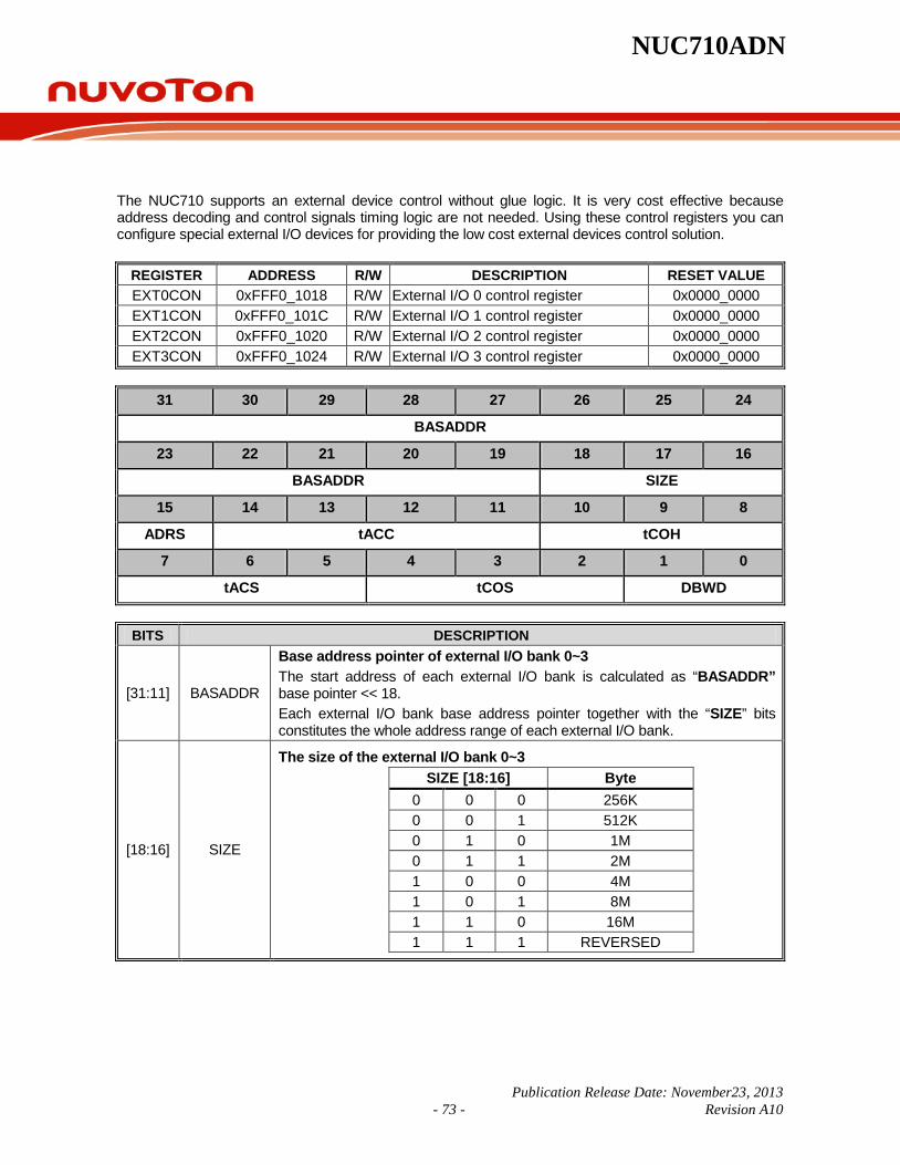
NUC710ADN
Publication Release Date: November23, 2013 - 73 - Revision A10
The NUC710 supports an external device control without glue logic. It is very cost effective because address decoding and control signals timing logic are not needed. Using these control registers you can configure special external I/O devices for providing the low cost external devices control solution.
REGISTER ADDRESS R/W DESCRIPTION RESET VALUE EXT0CON 0xFFF0_1018 R/W External I/O 0 control register 0x0000_0000 EXT1CON 0xFFF0_101C R/W External I/O 1 control register 0x0000_0000 EXT2CON 0xFFF0_1020 R/W External I/O 2 control register 0x0000_0000 EXT3CON 0xFFF0_1024 R/W External I/O 3 control register 0x0000_0000
31 30 29 28 27 26 25 24
BASADDR
23 22 21 20 19 18 17 16
BASADDR SIZE
15 14 13 12 11 10 9 8
ADRS tACC tCOH
7 6 5 4 3 2 1 0
tACS tCOS DBWD
BITS DESCRIPTION
[31:11] BASADDR
Base address pointer of external I/O bank 0~3 The start address of each external I/O bank is calculated as “BASADDR” base pointer << 18. Each external I/O bank base address pointer together with the “SIZE” bits constitutes the whole address range of each external I/O bank.
[18:16] SIZE
The size of the external I/O bank 0~3 SIZE [18:16] Byte
0 0 0 256K 0 0 1 512K 0 1 0 1M 0 1 1 2M 1 0 0 4M 1 0 1 8M 1 1 0 16M 1 1 1 REVERSED
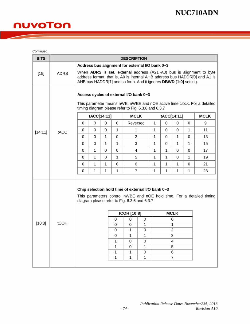
NUC710ADN
Publication Release Date: November235, 2013 - 74 - Revision A10
Continued.
BITS DESCRIPTION
[15] ADRS
Address bus alignment for external I/O bank 0~3 When ADRS is set, external address (A21~A0) bus is alignment to byte address format, that is, A0 is internal AHB address bus HADDR[0] and A1 is AHB bus HADDR[1] and so forth. And it ignores DBWD [1:0] setting.
[14:11] tACC
Access cycles of external I/O bank 0~3
This parameter means nWE, nWBE and nOE active time clock. For a detailed timing diagram please refer to Fig. 6.3.6 and 6.3.7
tACC[14:11] MCLK tACC[14:11] MCLK 0 0 0 0 Reversed 1 0 0 0 9
0 0 0 1 1 1 0 0 1 11
0 0 1 0 2 1 0 1 0 13
0 0 1 1 3 1 0 1 1 15
0 1 0 0 4 1 1 0 0 17
0 1 0 1 5 1 1 0 1 19
0 1 1 0 6 1 1 1 0 21
0 1 1 1 7 1 1 1 1 23
[10:8] tCOH
Chip selection hold time of external I/O bank 0~3 This parameters control nWBE and nOE hold time. For a detailed timing diagram please refer to Fig. 6.3.6 and 6.3.7
tCOH [10:8] MCLK 0 0 0 0 0 0 1 1 0 1 0 2 0 1 1 3 1 0 0 4 1 0 1 5 1 1 0 6 1 1 1 7
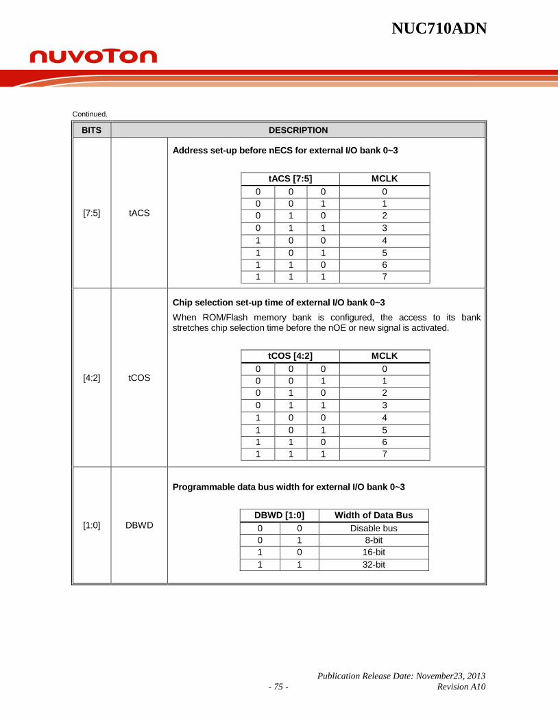
NUC710ADN
Publication Release Date: November23, 2013 - 75 - Revision A10
Continued.
BITS DESCRIPTION
[7:5] tACS
Address set-up before nECS for external I/O bank 0~3
tACS [7:5] MCLK 0 0 0 0 0 0 1 1 0 1 0 2 0 1 1 3 1 0 0 4 1 0 1 5 1 1 0 6 1 1 1 7
[4:2] tCOS
Chip selection set-up time of external I/O bank 0~3 When ROM/Flash memory bank is configured, the access to its bank stretches chip selection time before the nOE or new signal is activated.
tCOS [4:2] MCLK 0 0 0 0 0 0 1 1 0 1 0 2 0 1 1 3 1 0 0 4 1 0 1 5 1 1 0 6 1 1 1 7
[1:0] DBWD
Programmable data bus width for external I/O bank 0~3
DBWD [1:0] Width of Data Bus 0 0 Disable bus 0 1 8-bit 1 0 16-bit 1 1 32-bit
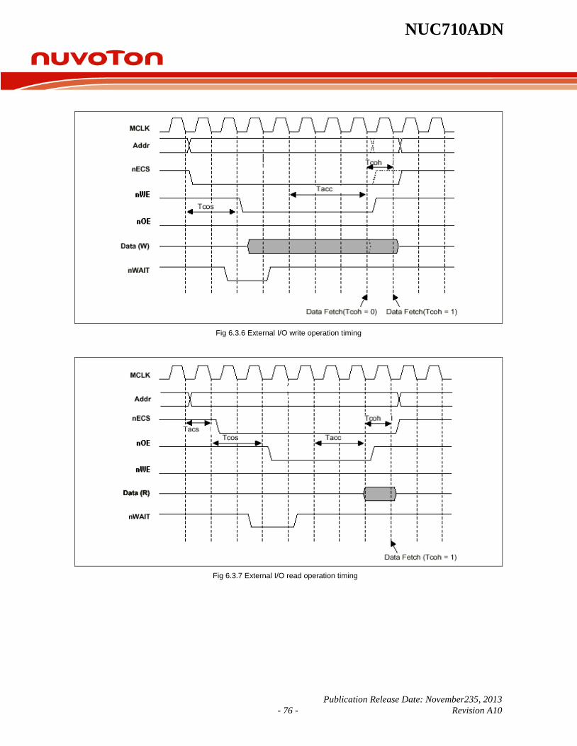
NUC710ADN
Publication Release Date: November235, 2013 - 76 - Revision A10
Fig 6.3.6 External I/O write operation timing
Fig 6.3.7 External I/O read operation timing
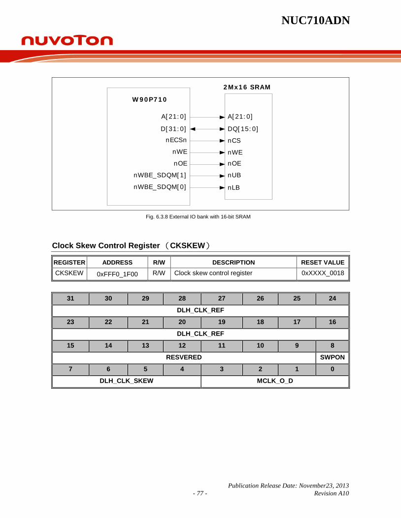
NUC710ADN
Publication Release Date: November23, 2013 - 77 - Revision A10
A[21:0]
D[31:0]
nWBE_SDQM[1]
nECSn
nWE
A[21:0]
DQ[15:0]
nOE
nCS
nWE
nOE
nUB
nLBnWBE_SDQM[0]
W90P710
2Mx16 SRAM
Fig. 6.3.8 External IO bank with 16-bit SRAM
Clock Skew Control Register (CKSKEW)
REGISTER ADDRESS R/W DESCRIPTION RESET VALUE CKSKEW 0xFFF0_1F00 R/W Clock skew control register 0xXXXX_0018
31 30 29 28 27 26 25 24
DLH_CLK_REF
23 22 21 20 19 18 17 16
DLH_CLK_REF
15 14 13 12 11 10 9 8
RESVERED SWPON
7 6 5 4 3 2 1 0
DLH_CLK_SKEW MCLK_O_D
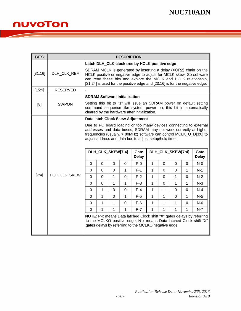
NUC710ADN
Publication Release Date: November235, 2013 - 78 - Revision A10
BITS DESCRIPTION
[31:16] DLH_CLK_REF
Latch DLH_CLK clock tree by HCLK positive edge SDRAM MCLK is generated by inserting a delay (XOR2) chain on the HCLK positive or negative edge to adjust for MCLK skew. So software can read these bits and explore the MCLK and HCLK relationship, [31:24] is used for the positive edge and [23:16] is for the negative edge.
[15:9] RESERVED -
[8] SWPON
SDRAM Software Initialization Setting this bit to “1” will issue an SDRAM power on default setting command sequence like system power on, this bit is automatically cleared by the hardware after initialization.
[7:4] DLH_CLK_SKEW
Data latch Clock Skew Adjustment Due to PC board loading or too many devices connecting to external addresses and data buses, SDRAM may not work correctly at higher frequencies (usually, > 80MHz) software can control MCLK_O_D[3:0] to adjust address and data bus to adjust setup/hold time.
DLH_CLK_SKEW[7:4] Gate Delay
DLH_CLK_SKEW[7:4] Gate Delay
0 0 0 0 P-0 1 0 0 0 N-0
0 0 0 1 P-1 1 0 0 1 N-1
0 0 1 0 P-2 1 0 1 0 N-2
0 0 1 1 P-3 1 0 1 1 N-3
0 1 0 0 P-4 1 1 0 0 N-4
0 1 0 1 P-5 1 1 0 1 N-5
0 1 1 0 P-6 1 1 1 0 N-6
0 1 1 1 P-7 1 1 1 1 N-7
NOTE: P-x means Data latched Clock shift “X” gates delays by referring to the MCLKO positive edge, N-x means Data latched Clock shift “X” gates delays by referring to the MCLKO negative edge.

NUC710ADN
Publication Release Date: November23, 2013 - 79 - Revision A10
Continued.
BITS DESCRIPTION
[3:0] MCLK_O_D
MCLK output delay adjustment
MCLK_O_D [3:0] Gate Delay
MCLK_O_D [3:0] Gate Delay
0 0 0 0 P-0 1 0 0 0 N-0
0 0 0 1 P-1 1 0 0 1 N-1
0 0 1 0 P-2 1 0 1 0 N-2
0 0 1 1 P-3 1 0 1 1 N-3
0 1 0 0 P-4 1 1 0 0 N-4
0 1 0 1 P-5 1 1 0 1 N-5
0 1 1 0 P-6 1 1 1 0 N-6
0 1 1 1 P-7 1 1 1 1 N-7
NOTE: “P-x” means MCLKO shift “X” gates delays by referring to the HCLK positive edge, “N-x” means MCLKO shift “X” gates delays by referring to the HCLK negative edge. MCLK is the output pin of MCLKO, which is an internal signal on chip.

NUC710ADN
Publication Release Date: November235, 2013 - 80 - Revision A10
6.4 Cache Controller NUC710 incorporates a 4KB Instruction cache, 4KB Data cache and an 8-word write buffer. To raise the cache-hit ratio, these two caches are configured two-way set associative addressing. Each cache has four words cache line size. When a miss occurs, four words must be fetched consecutively from external memory. The replacement algorithm is a LRU (Least Recently Used). If disabling the I-Cache / D-Cache, these cache memories can be treated as On-Chip RAM. NUC710 also provides a write buffer to improve system performance. The write buffer can buffer up to eight words of data.
6.4.1 On-Chip RAM If I-Cache or D-Cache is disabled, it can serve as On-Chip RAM. If D-Cache is disabled, there is a 4KB On-Chip RAM, its start address is 0xFFE01000. If I-Cache is disabled, there has 4KB On-Chip RAM and the start address of this RAM is 0xFFE00000. If both the I-Cache and D-Cache are disabled, it has 8KB On-Chip RAM starting from 0xFFE00000. The size of On-Chip RAM is depended on the I-Cache and D-Cache enable bits ICAEN, DCAEN in Cache Control Register (CAHCON).
Table6.4.1 The size and start address of On-Chip RAM
ICAEN DCAEN ON-CHIP RAM
SIZE START ADDRESS 0 0 8KB 0xFFE0_0000
0 1 4KB 0xFFE0_0000
1 0 4KB 0xFFE0.1000
1 1 Unavailable
6.4.2 Non-Cacheable Area Although the cache affects the entire 2GB system memory, it is sometimes necessary to define non-cacheable areas when the consistency of data stored in memory and the cache must be ensured. To support this, NUC710 provides a non-cacheable area control bit in address field A[31]. If A[31] in the ROM/FLASH, SDRAM, or external I/O bank’s access address is “0”, then the accessed data is cacheable. If the A [31] value is “1”, the accessed data is non-cacheable.
NUC710ADN
Publication Release Date: November23, 2013 - 81 - Revision A10
6.4.3 Instruction Cache The Instruction cache (I-cache) is a 4K bytes two-way set associative cache. The cache organization is 128 sets, two lines per set, and four words per line. Cache lines are aligned on 4-word boundaries in memory. The cache access cycle begins with an instruction request from the instruction unit in the core. In the case of a cache hit, the instruction is delivered to the instruction unit. In case of a cache miss, the cache initiates a burst read cycle on the internal bus with the address of the requested instruction. The first word received from the bus is the requested instruction. The cache forwards this instruction to the instruction unit of the core as soon as it is received from the internal bus. A cache line is then selected to receive the data that will be coming from the bus. A least recently used (LRU) replacement algorithm is used to select a line when no empty lines are available. When I-Cache is disabled, the cache memory is served as 4KB On-chip RAM. The I-Cache is always disabled on reset.
The following is a list of the instruction cache features: 4K bytes instruction cache Two-way set associative Four words in a cache line LRU replacement policy Lockable on a per-line basis Critical word first, burst access
Instruction Cache Operation On an instruction fetch, bits 10-4 of the instruction’s address point into the cache to retrieve the tags and data of one set. The tags are then compared against bits 30-11 of the instruction’s address. If a match is found and the matched entry is valid, then it is a cache hit. If neither tags match or the matched tag is invalid, it is a cache miss.
Instruction Cache Hit In case of a cache hit, bits 3-2 of the instruction address is used to select one word from the cache line with matching tags. The instruction is immediately transferred to the core instruction unit.
Instruction Cache Miss On an instruction cache miss, the address of the missed instruction is driven on the internal bus with a 4-word burst transfer read request. A cache line is then selected to receive the data that will be coming from the bus. The selection algorithm gives first priority to invalid lines. If neither of the two lines in the selected set is invalid, then the least recently used line is selected for replacement. Locked lines are never replaced. The transfer begins with the word requested by the instruction unit (critical word first), followed by the remaining words of the line, then by the word at the beginning of the lines (wraparound).
Instruction Cache Flushing NUC710 does not support external memory snooping. Therefore, if self-modifying code is written, the instructions in the I-Cache may become invalid. The entire I-Cache can be flushed by software in one operation, or can be flushed one line at a time by setting either CAHCON register bit FLHS or ICAH register bit FLHA. As flushing the cache line, the “V” bit of the line is cleared to “0”. The I-Cache is automatically flushed during reset.

NUC710ADN
Publication Release Date: November235, 2013 - 82 - Revision A10
Instruction Cache Load and Lock NUC710 supports a cache-locking feature that can be used to lock critical sections of code into I-Cache to guarantee quick access. Lockdown can be performed with a granularity of one cache line. The smallest space that can be locked down is 4 words. After a line is locked, it operates as a regular instruction SRAM. Locked lines are not replaced during cache-misses and are not affected by flush-per-line commands.
To load and lock instructions, see the following procedure: 1. Write the start address of the instructions to be locked into CAHADR register.
2. Set LDLK and ICAH bits in the CAHCON register.
3. Increase the address by 16 and write into CAHADR register.
4. Set LDLK and ICAH bits in the CAHCON register. 5. Repeat steps 3 and 4 until the desired instructions are all locked.
When using the I-Cache load and lock command the following should be taken into consideration: Programs executing load and lock operations should be held in non-cacheable memory. The cache should be enabled and interrupts should be disabled. Software must flush the cache before executing load and lock to ensure that the code to be locked
down is not already in the cache.
Instruction Cache Unlock The unlock operation is used to unlock previously locked cache lines. After unlocking, the “L” bit of the line is cleared to “0”. NUC710 has two unlock commands, unlock line and unlock all.
The unlock line operation is performed on a cache line. In case the line is found in the cache, it is unlocked and operates as a regular valid cache line. In case the line is not found in the cache, nothing is executed and the command terminates without raising an exception. To unlock one line, the following unlock line sequence should be followed: 1. Write the address of the line to be unlocked into the CAHADR Register.
2. Set the ULKS and ICAH bits in the CAHCON register.
The unlock all operation is used to unlock the whole I-Cache. This operation is performed on all cache lines. In case a line is locked, it is unlocked and starts to operate as regular valid cache line. In case a line is not locked or if it is invalid, no operation is performed. To unlock the whole cache, set the ULKA and ICAH bits.
NUC710ADN
Publication Release Date: November23, 2013 - 83 - Revision A10
6.4.4 Data Cache NUC710 data cache (D-Cache) is a 4KB two-way set associative cache. The cache organization is 128 sets, two lines per set, and four words per line. Cache lines are aligned on 4-word boundaries in memory. The cache is designed for buffer write-through mode of operation and a least recently used (LRU) replacement algorithm is used to select a line when no empty lines are available. When D-Cache is disabled, the cache memory is served as 4KB On-chip RAM. The D-Cache is always disabled on reset. The following is a list of the data cache features: 4K bytes data cache Two-way set associative Four words in a cache line LRU replacement policy Lockable on a per-line basis Critical word first, burst access Buffer Write-through mode 8 words write buffer Drain write buffer
Data Cache Operation On a data fetch, bits 10-4 of the data’s address point into the cache to retrieve the tags and data of one set. The tags from both are then compared against bits 30-11 of the data’s address. If a match is found and the matched entry is valid, then it is a cache hit. If neither tags match or the matched tag is invalid, it is a cache miss.
Data Cache Read Read Hit: On a cache hit, the requested word is immediately transferred to the core.
Read Miss: A line in the cache is selected to hold the data to be fetched from memory. The selection algorithm gives first priority to idate lines in the selected set is invalid, then one of the lines is selected by the LRU algorithm to replace. The transfer begins with the aligned word containing the missed data (critical word first), followed bnvalid lines. If both lines are invalid the way zero line is selected first. If neither of the two candiy the remaining word in the line, then by the word at the beginning of the line (wraparound). As the missed word is received from the bus, it is delivered directly to the core.
Data Cache Write In buffer write-through mode, store operations always update memory. The buffer write-through mode is used when external memory and internal cache images must always agree.

NUC710ADN
Publication Release Date: November235, 2013 - 84 - Revision A10
Write Hit: Data is written into both the cache and write buffer. The processor then continues to access the cache, while the cache controller simultaneously downloads the contents of the write buffer to main memory. This reduces the effective write memory cycle time from the time required for a main memory cycle to the cycle time of the high-speed cache. Write Miss: Data is only written into the write buffer, and not to the cache (write no allocate).
Data Cache Flushing NUC710 allows the data cache to be flushed under software control. The data cache may be invalidated by writing flush line (FLHS) or flush all (FLHA) commands to the CAHCON register. Flushing the entire D-Cache also flushes any locked down code. As flushing the data cache, the “V” bit of the line is cleared to “0”. The D-cache is automatically flushed during reset.
Data Cache Load and Lock NUC710 supports a cache-locking feature that can be used to lock critical sections of data into D-Cache to guarantee quick access. Lockdown can be performed with a granularity of one cache line. The smallest space, which can be locked down, is 4 words. After a line is locked, it operates as a regular SRAM instruction. The locked lines are not replaced during misses and are not affected by flush-per-line commands. To load and lock data, see the following procedure: 1. Write the start address of the data to be locked into CAHADR register.
2. Set LDLK and DCAH bits in the CAHCON register.
3. Increase the address by 16 and write into CAHADR register.
4. Set LDLK and DCAH bits in the CAHCON register. 5. Repeat steps 3 and 4, until all the desired data are locked.
When using D-Cache load and lock command, the following should be taken into consideration: The programs executing load and lock operation should be held in a non-cacheable area of
memory. The cache should be enabled and interrupts disabled. Software must flush the cache before executing load and lock to ensure that the data to be locked
down is not already in the cache.
Data Cache Unlock The unlock operation is used to unlock previously locked cache lines. After unlocking, the “L” bit of the line is cleared to “0”. NUC710 has two unlock commands, unlock line and unlock all. The unlock line operation is performed on a cache line granularity. In case the line is found in the cache, it is unlocked and starts to operate as a regular valid cache line. In case the line is not found in the cache, nothing is executed and the command terminates without raising an exception. To unlock one line the following unlock line sequence should be followed:
1. Write the address of the line to be unlocked into the CAHADR Register.
2. Set the ULKS and DCAH bits in the CAHCON register.
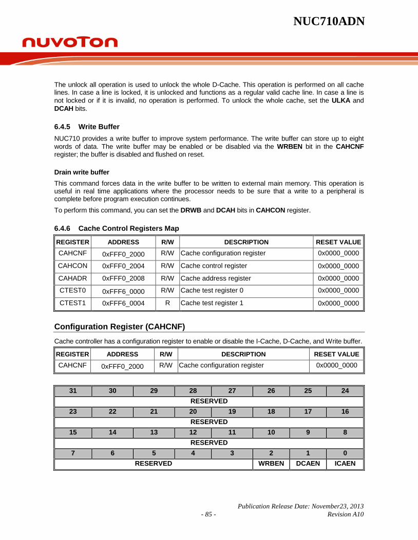
NUC710ADN
Publication Release Date: November23, 2013 - 85 - Revision A10
The unlock all operation is used to unlock the whole D-Cache. This operation is performed on all cache lines. In case a line is locked, it is unlocked and functions as a regular valid cache line. In case a line is not locked or if it is invalid, no operation is performed. To unlock the whole cache, set the ULKA and DCAH bits.
6.4.5 Write Buffer NUC710 provides a write buffer to improve system performance. The write buffer can store up to eight words of data. The write buffer may be enabled or be disabled via the WRBEN bit in the CAHCNF register; the buffer is disabled and flushed on reset.
Drain write buffer This command forces data in the write buffer to be written to external main memory. This operation is useful in real time applications where the processor needs to be sure that a write to a peripheral is complete before program execution continues. To perform this command, you can set the DRWB and DCAH bits in CAHCON register.
6.4.6 Cache Control Registers Map
REGISTER ADDRESS R/W DESCRIPTION RESET VALUE CAHCNF 0xFFF0_2000 R/W Cache configuration register 0x0000_0000
CAHCON 0xFFF0_2004 R/W Cache control register 0x0000_0000
CAHADR 0xFFF0_2008 R/W Cache address register 0x0000_0000
CTEST0 0xFFF6_0000 R/W Cache test register 0 0x0000_0000
CTEST1 0xFFF6_0004 R Cache test register 1 0x0000_0000
Configuration Register (CAHCNF) Cache controller has a configuration register to enable or disable the I-Cache, D-Cache, and Write buffer.
REGISTER ADDRESS R/W DESCRIPTION RESET VALUE CAHCNF 0xFFF0_2000 R/W Cache configuration register 0x0000_0000
31 30 29 28 27 26 25 24
RESERVED 23 22 21 20 19 18 17 16
RESERVED 15 14 13 12 11 10 9 8
RESERVED 7 6 5 4 3 2 1 0
RESERVED WRBEN DCAEN ICAEN
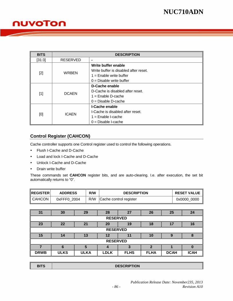
NUC710ADN
Publication Release Date: November235, 2013 - 86 - Revision A10
BITS DESCRIPTION [31:3] RESERVED -
[2] WRBEN
Write buffer enable Write buffer is disabled after reset. 1 = Enable write buffer 0 = Disable write buffer
[1] DCAEN
D-Cache enable D-Cache is disabled after reset. 1 = Enable D-cache 0 = Disable D-cache
[0] ICAEN
I-Cache enable I-Cache is disabled after reset. 1 = Enable I-cache 0 = Disable I-cache
Control Register (CAHCON) Cache controller supports one Control register used to control the following operations. Flush I-Cache and D-Cache Load and lock I-Cache and D-Cache Unlock I-Cache and D-Cache Drain write buffer These commands set CAHCON register bits, and are auto-clearing. I.e. after execution, the set bit automatically returns to “0”.
REGISTER ADDRESS R/W DESCRIPTION RESET VALUE CAHCON 0xFFF0_2004 R/W Cache control register 0x0000_0000
31 30 29 28 27 26 25 24 RESERVED
23 22 21 20 19 18 17 16 RESERVED
15 14 13 12 11 10 9 8 RESERVED
7 6 5 4 3 2 1 0 DRWB ULKS ULKA LDLK FLHS FLHA DCAH ICAH
BITS DESCRIPTION
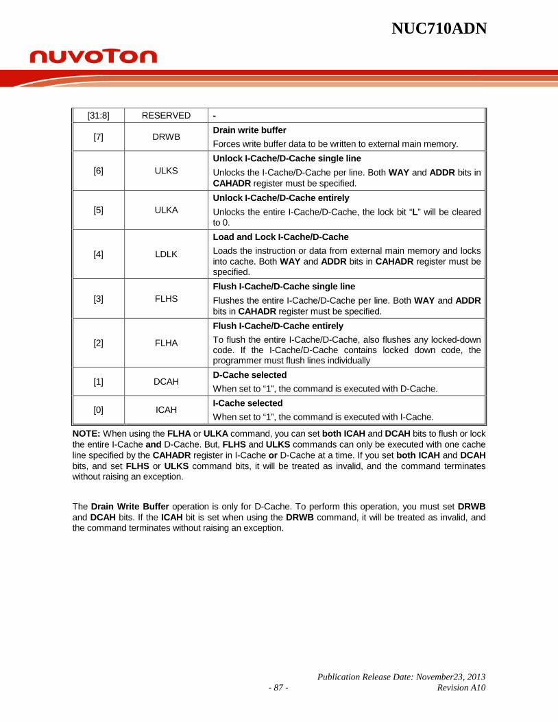
NUC710ADN
Publication Release Date: November23, 2013 - 87 - Revision A10
[31:8] RESERVED -
[7] DRWB Drain write buffer Forces write buffer data to be written to external main memory.
[6] ULKS Unlock I-Cache/D-Cache single line Unlocks the I-Cache/D-Cache per line. Both WAY and ADDR bits in CAHADR register must be specified.
[5] ULKA Unlock I-Cache/D-Cache entirely Unlocks the entire I-Cache/D-Cache, the lock bit “L” will be cleared to 0.
[4] LDLK
Load and Lock I-Cache/D-Cache Loads the instruction or data from external main memory and locks into cache. Both WAY and ADDR bits in CAHADR register must be specified.
[3] FLHS Flush I-Cache/D-Cache single line Flushes the entire I-Cache/D-Cache per line. Both WAY and ADDR bits in CAHADR register must be specified.
[2] FLHA
Flush I-Cache/D-Cache entirely To flush the entire I-Cache/D-Cache, also flushes any locked-down code. If the I-Cache/D-Cache contains locked down code, the programmer must flush lines individually
[1] DCAH D-Cache selected When set to “1”, the command is executed with D-Cache.
[0] ICAH I-Cache selected When set to “1”, the command is executed with I-Cache.
NOTE: When using the FLHA or ULKA command, you can set both ICAH and DCAH bits to flush or lock the entire I-Cache and D-Cache. But, FLHS and ULKS commands can only be executed with one cache line specified by the CAHADR register in I-Cache or D-Cache at a time. If you set both ICAH and DCAH bits, and set FLHS or ULKS command bits, it will be treated as invalid, and the command terminates without raising an exception. The Drain Write Buffer operation is only for D-Cache. To perform this operation, you must set DRWB and DCAH bits. If the ICAH bit is set when using the DRWB command, it will be treated as invalid, and the command terminates without raising an exception.

NUC710ADN
Publication Release Date: November235, 2013 - 88 - Revision A10
Address Register (CAHADR) NUC710 Cache Controller supports one address register. This address register is used with the command set in the control register (CAHCON) by specifying instruction/data address.
REGISTER ADDRESS R/W DESCRIPTION RESET VALUE CAHADR 0xFFF0_2008 R/W Cache address register 0x0000_0000
31 30 29 28 27 26 25 24
WAY ADDR 23 22 21 20 19 18 17 16
ADDR 15 14 13 12 11 10 9 8
ADDR 7 6 5 4 3 2 1 0
ADDR
BITS DESCRIPTION
[31] WAY Way selection 0 = Way0 is selected 1 = Way1 is selected
[30:0] ADDR The absolute address of instruction or data
Cache Test Register 0 (CTEST0) Cache test control register enables/disables cache and tag RAM testing. In addition, this register controls the built-in self-test (BIST) SRAM function.
REGISTER ADDRESS R/W DESCRIPTION RESET VALUE CTEST0 0xFFF6_0000 R/W Cache test register 0 0x0000_0000
31 30 29 28 27 26 25 24
RESERVED 23 22 21 20 19 18 17 16
RESERVED 15 14 13 12 11 10 9 8
BISTEN RESERVED BST_GP3 BST_GP2 BST_GP1 BST_GP0 7 6 5 4 3 2 1 0
RESERVED CATEST

NUC710ADN
Publication Release Date: November23, 2013 - 89 - Revision A10
BITS DESCRIPTION [31:16] RESERVED -
[15] BISTEN BIST mode enable When set to “1”, BIST mode will be enabled and the selected memory groups begins BIST testing.
[14:12] RESERVED -
[11] BIST_GP3 Memory group 3 is selected for BIST testing When set to “1”, memory group 3, including data cache tag ram way 0 and way 1, are selected for BIST testing.
[10] BIST_GP2 Memory group 2 is selected for BIST testing When set to “1”, memory group 2, including program cache tag ram way 0 and way 1, are selected for BIST testing.
[9] BIST_GP1 Memory group 1 is selected for BIST testing When set to “1”, memory group 1, including data cache ram way 0 and way 1, are selected for BIST testing.
[8] BIST_GP0 Memory group 0 is selected for BIST testing When set to “1”, memory group 0, including program cache ram way 0 and way 1, are selected for BIST testing.
[7:0] RESERVED - ** Note: The 4 memory groups can be selected and tested simultaneously by BIST.
Cache Test Register 1 (CTEST1) Cache Test Register that will be read back to provide the status of cache RAM BIST. The current testing status is stored in this register.
REGISTER ADDRESS R/W DESCRIPTION RESET VALUE CTEST1 0xFFF6_0004 R Cache test register 1 0x0000_0000
31 30 29 28 27 26 25 24
FINISH RESERVED
23 22 21 20 19 18 17 16
RESERVED
15 14 13 12 11 10 9 8
RESERVED
7 6 5 4 3 2 1 0
BFAIL7 BFAIL6 BFAIL5 BFAIL4 BFAIL3 BFAIL2 BFAIL1 BFAIL0
BITS DESCRIPTION
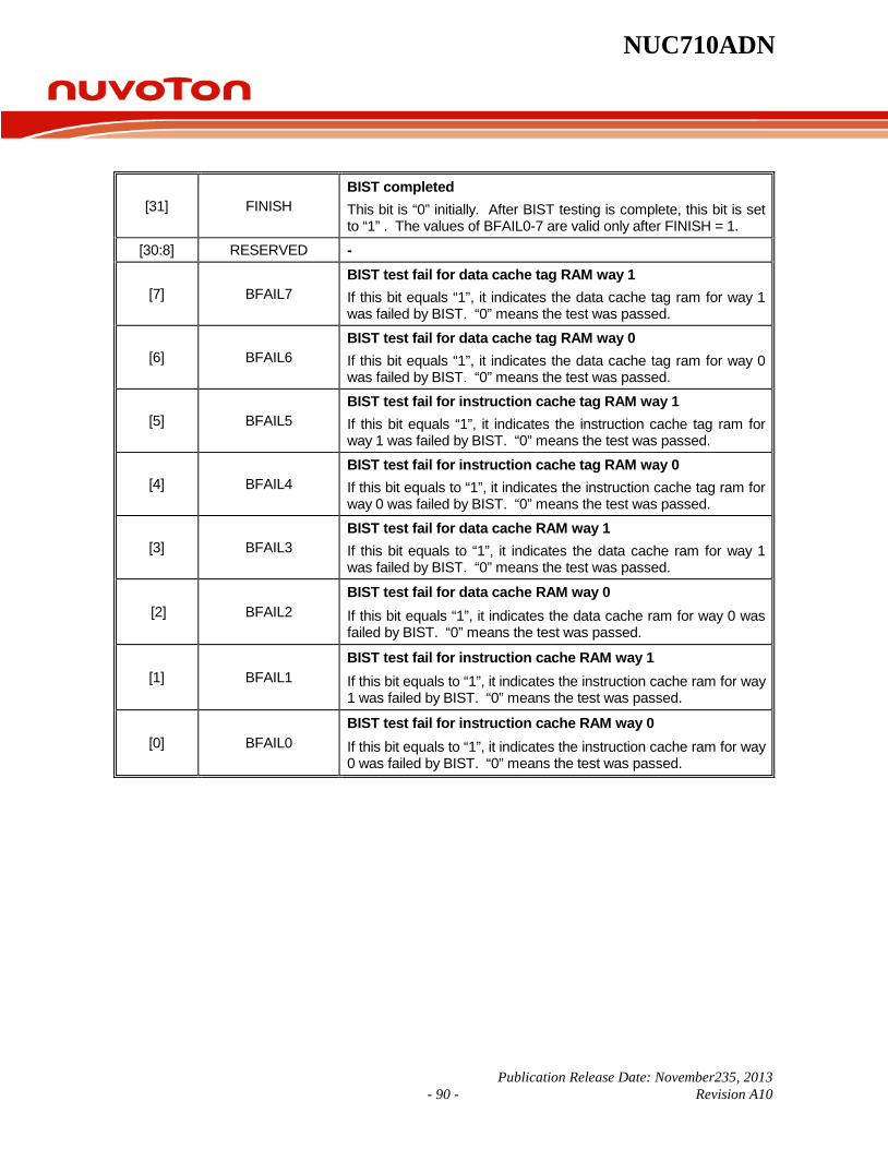
NUC710ADN
Publication Release Date: November235, 2013 - 90 - Revision A10
[31] FINISH BIST completed This bit is “0” initially. After BIST testing is complete, this bit is set to “1” . The values of BFAIL0-7 are valid only after FINISH = 1.
[30:8] RESERVED -
[7] BFAIL7 BIST test fail for data cache tag RAM way 1 If this bit equals “1”, it indicates the data cache tag ram for way 1 was failed by BIST. “0” means the test was passed.
[6] BFAIL6 BIST test fail for data cache tag RAM way 0 If this bit equals “1”, it indicates the data cache tag ram for way 0 was failed by BIST. “0” means the test was passed.
[5] BFAIL5 BIST test fail for instruction cache tag RAM way 1 If this bit equals “1”, it indicates the instruction cache tag ram for way 1 was failed by BIST. “0” means the test was passed.
[4] BFAIL4 BIST test fail for instruction cache tag RAM way 0 If this bit equals to “1”, it indicates the instruction cache tag ram for way 0 was failed by BIST. “0” means the test was passed.
[3] BFAIL3 BIST test fail for data cache RAM way 1 If this bit equals to “1”, it indicates the data cache ram for way 1 was failed by BIST. “0” means the test was passed.
[2] BFAIL2 BIST test fail for data cache RAM way 0 If this bit equals “1”, it indicates the data cache ram for way 0 was failed by BIST. “0” means the test was passed.
[1] BFAIL1 BIST test fail for instruction cache RAM way 1 If this bit equals to “1”, it indicates the instruction cache ram for way 1 was failed by BIST. “0” means the test was passed.
[0] BFAIL0 BIST test fail for instruction cache RAM way 0 If this bit equals to “1”, it indicates the instruction cache ram for way 0 was failed by BIST. “0” means the test was passed.
NUC710ADN
Publication Release Date: November23, 2013 - 91 - Revision A10
6.5 Ethernet MAC Controller
Overview NUC710 provides an Ethernet MAC Controller (EMC) for LAN application. This EMC has a DMA controller, transmit FIFO, and receive FIFO.
The Ethernet MAC controller consists of an IEEE 802.3/Ethernet protocol engine with internal CAM function for Ethernet MAC address recognition, Transmit-FIFO, Receive-FIFO, TX/RX state machine controller and status controller. The EMC only supports RMII (Reduced MII) interface to connect with PHY operating on 50MHz REF_CLK.
Features Supports IEEE Std. 802.3 CSMA/CD protocol. Supports both half and full duplex for 10M/100M bps operation. Supports RMII interface. Supports MII Management function. Supports pause and remote pause function for flow control. Supports long frame (more than 1518 bytes) and short frame (less than 64 bytes) reception. Supports 16 entries CAM function for Ethernet MAC address recognition. Supports internal loop back mode for diagnostics. Supports 256 bytes embedded transmit and receive FIFO. Supports DMA function.
6.5.1 EMC Functional Description
MII Management State Machine The MII management function of EMC is compliant with IEEE 802.3 Std. Through the MII management interface, software can access the control and status registers of the external PHY chip. The two programmable registers MIID (MAC MII Management Data Register) and MIIDA (MAC MII Management Data Control and Address Register) are for MII management functions. Setting the BUSY bit of the MIIDA register triggers the MII management state machine. After the MII management cycle is finished, the BUSY bit is automatically cleared.
Media Access Control (MAC) The NUC710 MAC function fully meets the requirements defined in the IEEE802.3u specification. The following paragraphs describe the frame structure and data reception and transmission operations. The transmission data frame sent from the transmit DMA are encapsulated by the MAC before transmitting onto the MII bus. The data sent is assembled with preamble, the start frame delimiter (SFD), the frame check sequence and padding to ensure the 64-byte minimum frame size and CRC sequence. The outgoing frame format is as follows:
110101010 --- 10101010 10101011 d0 d1 d2 - dn Padding CRC31 CRC30 --- CRC0
As mentioned by the above format, the preamble is a consecutive 7-byte long with the pattern “10101010” and the SFD is a one byte 10101011 data. The padding data will be all 0 value if the sent

NUC710ADN
Publication Release Date: November235, 2013 - 92 - Revision A10
data frame is less than 64 bytes. The padding disable function specified in the bit P of the transmit descriptor is used to control if the MAC needs to pad data at the end of frame data or not when the transmitted data frame is less than 64 bytes. The padding data will not be appended if the padding disable bit is set to be high. The bits CRC0 ... CRC31 are the 32 bits cyclic redundancy check (CRC) sequence. The CRC encoding is defined by the following polynomial specified by the IEEE802.3. This 32 bits CRC appending function will be disabled if the Inhibit CRC of the transmission descriptor is set to high. The MAC also performs many other transmission functions specified by IEEE802.3, including the inter-frame spacing function, collision detection, collision enforcement, collision back-off and retransmission. The collision back-off timer is a function of the integer slot time, 512 bit times. The number of slot times to delay between the current transmission attempt and the next attempt is determined by a uniformly distributed random integer algorithm specified by IEEE802.3. The MAC performs the receive functions specified by IEEE 802.3 including the address recognition function, the frame check sequence validation, the frame disassembly, framing and collision filtering.
EMC Descriptors A linked-list data structure called a descriptor is used to keep the control, status and data
information of each frame. Through the descriptor, CPU and EMC exchange the information for frame reception and transmission.
Two different descriptors are defined in NUC710. One named as Rx descriptor for frame reception and the other names as Tx descriptor for frame transmission. Each Rx descriptor consists of four words. There is much information stored in these descriptors, and details are as follows:
6.5.1.1 Rx Buffer Descriptor 31
30
29 1
6 15
0 O Rx Status Receive Byte Count
Receive Buffer Starting Address BO Reserved
Next Rx Descriptor Starting Address

NUC710ADN
Publication Release Date: November23, 2013 - 93 - Revision A10
Rx Descriptor Word 0
31 30 29 28 27 26 25 24 Owner Reserved
23 22 21 20 19 18 17 16 Reserved RP ALIE RXGD PTLE Reserved CRCE RXINTR
15 14 13 12 11 10 9 8 RBC
7 6 5 4 3 2 1 0 RBC
Owner [31:30]: Ownership The ownership field defines if the CPU or EMC is the owner of each Rx descriptor. Only the owner has write access to the Rx descriptor. Otherwise the descriptor is read-only. 00: The owner is CPU 01: Undefined 10: The owner is EMC 11: Undefined If the O=2’b10 indicates the EMC RxDMA is the owner of Rx descriptor and the Rx descriptor is available for frame reception. After the frame reception completed, if the frame needs NAT translation, EMC RxDMA modifies the ownership field to 2’b11. Otherwise, the ownership field is modified to 2’b00. If O=2’b00 indicates the CPU is the owner of Rx descriptor, after the CPU completes processing the frame it modifies the ownership field to 2’b10 and releases the Rx descriptor to EMC RxDMA. Rx Status [29:16]: Receive Status This field stores the status for frame reception. All status bits are updated by the EMC. In the receive status, bits 29 to 23 are undefined and reserved for the future. RP [22]: Runt Packet The RP indicates the frame stored in the data buffer pointed to by the Rx descriptor is a short frame (frame length is less than 64 bytes). 1’b0: Frame is not a short frame. 1’b1: Frame is a short frame. ALIE [21]: Alignment Error The ALIE indicates the frame stored in the data buffer pointed to by the Rx descriptor is not a multiple of byte. 1’b0: Frame is a multiple of byte. 1’b1: Frame is not a multiple of byte.

NUC710ADN
Publication Release Date: November235, 2013 - 94 - Revision A10
RXGD [20]: Frame Reception Complete The RXGD indicates the frame reception has completed and stored in the data buffer pointed by the Rx descriptor. 1’b0: Frame reception is incomplete. 1’b1: Frame reception complete.
PTLE [19]: Packet Too Long The PTLE indicates the frame stored in the data buffer pointed to by the Rx descriptor is a long frame (frame length is greater than 1518 bytes). 1’b0: The frame is not a long frame. 1’b1: The frame is a long frame.
CRCE [17]: CRC Error CRCE indicates the frame stored in the data buffer pointed to by the Rx descriptor caused a CRC error. 1’b0: No error. 1’b1: Frame caused CRC error.
RXINTR [16]: Receive Interrupt The RXINTR indicates the frame stored in the data buffer pointed by Rx descriptor caused an interrupt. 1’b0: No interrupt. 1’b1: Frame caused an interrupt.
RBC [15:0]: Receive Byte Count RBC indicates the byte count of the frame stored in the data buffer pointed to by Rx descriptor. The four-byte CRC field is also included in the receive byte count. But if the SPCRC of register MCMDR is enabled, the four-byte CRC field is excluded from the receive byte count.
Rx Descriptor Word 1
31 30 29 28 27 26 25 24 RXBSA
23 22 21 20 19 18 17 16 RXBSA
15 14 13 12 11 10 9 8 RXBSA
7 6 5 4 3 2 1 0 RXBSA BO
RXBSA [31:2]: Receive Buffer Starting Address
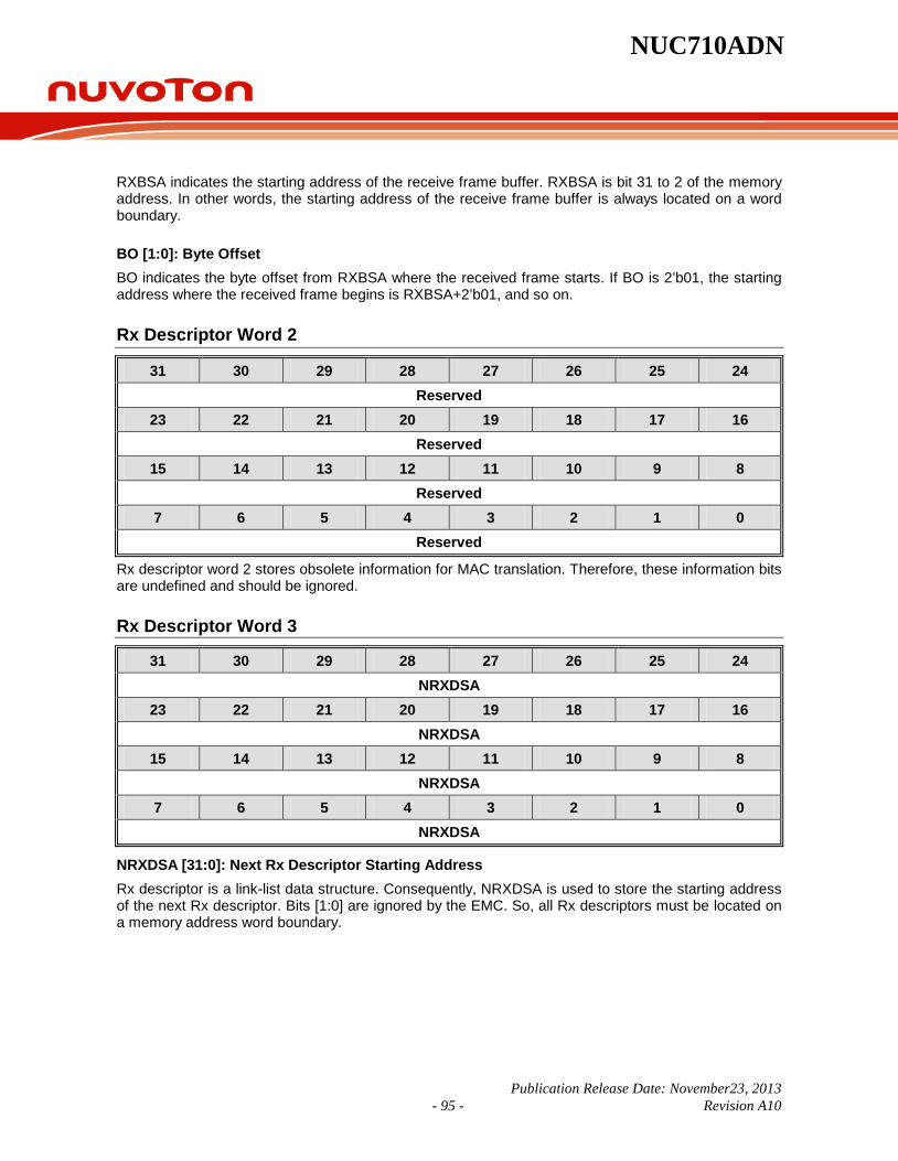
NUC710ADN
Publication Release Date: November23, 2013 - 95 - Revision A10
RXBSA indicates the starting address of the receive frame buffer. RXBSA is bit 31 to 2 of the memory address. In other words, the starting address of the receive frame buffer is always located on a word boundary.
BO [1:0]: Byte Offset BO indicates the byte offset from RXBSA where the received frame starts. If BO is 2’b01, the starting address where the received frame begins is RXBSA+2’b01, and so on.
Rx Descriptor Word 2
31 30 29 28 27 26 25 24 Reserved
23 22 21 20 19 18 17 16 Reserved
15 14 13 12 11 10 9 8 Reserved
7 6 5 4 3 2 1 0 Reserved
Rx descriptor word 2 stores obsolete information for MAC translation. Therefore, these information bits are undefined and should be ignored.
Rx Descriptor Word 3
31 30 29 28 27 26 25 24 NRXDSA
23 22 21 20 19 18 17 16 NRXDSA
15 14 13 12 11 10 9 8 NRXDSA
7 6 5 4 3 2 1 0 NRXDSA
NRXDSA [31:0]: Next Rx Descriptor Starting Address Rx descriptor is a link-list data structure. Consequently, NRXDSA is used to store the starting address of the next Rx descriptor. Bits [1:0] are ignored by the EMC. So, all Rx descriptors must be located on a memory address word boundary.

NUC710ADN
Publication Release Date: November235, 2013 - 96 - Revision A10
6.5.1.2 Tx Buffer Descriptor 31
30 1
6 15
3 2
1
0
O Reserved I C P Transmit Buffer Starting Address BO
Tx Status Transmit Byte Count Next Tx Descriptor Starting Address
Tx Descriptor Word 0
31 30 29 28 27 26 25 24 Owner Reserved
23 22 21 20 19 18 17 16 Reserved
15 14 13 12 11 10 9 8 Reserved
7 6 5 4 3 2 1 0 Reserved IntEn CRCApp PadEn
Owner [31]: Ownership The ownership field defines which of the CPU or EMC is the owner of each Tx descriptor. Only the owner has right to modify the Tx descriptor, otherwise the Tx descriptor is read-only. 0: The owner is the CPU 1: The owner is the EMC If O=1’b1 indicates the EMC TxDMA is the owner, and the Tx descriptor is available for frame transmission, then after the frame transmission complete, the EMC TxDMA modifies the ownership field to 1’b0 and returns ownership of the Tx descriptor to the CPU. If O=1’b0 indicates the CPU is the owner, then after the CPU prepares a new frame for transmission, it modifies the ownership field to 1’b1 and releases the Tx descriptor to EMC TxDMA. IntEn [2]: Transmit Interrupt Enable IntEn controls the interrupt trigger circuit after frame transmission complete. If IntEn is enabled, the EMC will trigger interrupt after frame transmission complete. Otherwise, the interrupt is not triggered. 1’b0: Frame transmission interrupt is masked. 1’b1: Frame transmission interrupt is enabled.
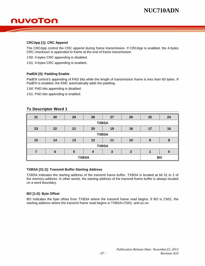
NUC710ADN
Publication Release Date: November23, 2013 - 97 - Revision A10
CRCApp [1]: CRC Append The CRCApp control the CRC append during frame transmission. If CRCApp is enabled, the 4-bytes CRC checksum is appended to frame at the end of frame transmission. 1’b0: 4-bytes CRC appending is disabled. 1’b1: 4-bytes CRC appending is enabled. PadEN [0]: Padding Enable PadEN control’s appending of PAD bits while the length of transmission frame is less than 60 bytes. If PadEN is enabled, the EMC automatically adds the padding. 1’b0: PAD bits appending is disabled. 1’b1: PAD bits appending is enabled.
Tx Descriptor Word 1
31 30 29 28 27 26 25 24 TXBSA
23 22 21 20 19 18 17 16 TXBSA
15 14 13 12 11 10 9 8 TXBSA
7 6 5 4 3 2 1 0 TXBSA BO
TXBSA [31:2]: Transmit Buffer Starting Address TXBSA indicates the starting address of the transmit frame buffer. TXBSA is located at bit 31 to 2 of the memory address. In other words, the starting address of the transmit frame buffer is always located on a word boundary. BO [1:0]: Byte Offset BO indicates the byte offset from TXBSA where the transmit frame read begins. If BO is 2’b01, the starting address where the transmit frame read begins is TXBSA+2’b01, and so on.

NUC710ADN
Publication Release Date: November235, 2013 - 98 - Revision A10
Tx Descriptor Word 2
31 30 29 28 27 26 25 24 CCNT Reserved SQE PAU TXHA
23 22 21 20 19 18 17 16 LC TXABT NCS EXDEF TXCP Reserved DEF TXINTR 15 14 13 12 11 10 9 8
TBC 7 6 5 4 3 2 1 0
TBC
CCNT [31:28]: Collision Count CCNT indicates the how many collisions occurred consecutively during packet transmission. If the packet incurred 16 consecutive collisions during transmission, the CCNT is 4’h0 and bit TXABT is set to 1. SQE [26]: SQE Error SQE indicates an SQE error was found at the end of packet transmission on 10Mbps half-duplex mode. The SQE error check is only performed when both EnSQE bits of the MCMDR are enabled and the EMC operates in 10Mbps half-duplex mode. 1’b0: No SQE error found at the end of packet transmission. 1’b0: SQE error found at the end of packet transmission. PAU [25]: Transmission Paused PAU INDICATES THE NEXT NORMAL PACKET transmission process is temporally paused because the EMC received a PAUSE control frame, or S/W set bit SDPZ of MCMDR and requests the EMC to transmit a PAUSE control frame out. 1’b0: Next normal packet transmission process will continue. 1’b1: Next normal packet transmission process is paused. TXHA [24]: Transmission Halted TXHA indicates the next normal packet transmission process is halted because the bit TXON of MCMDR is disabled in S/W. 1’b0: Next normal packet transmission process will continue. 1’b1: Next normal packet transmission process is halted.
NUC710ADN
Publication Release Date: November23, 2013 - 99 - Revision A10
LC [23]: Late Collision LC indicates the collision occurred outside of the 64-byte collision window. This means that after the 64 bytes of the frame was transmitted, the collision still occurred. The late collision check is only performed when the EMC is operating in half-duplex mode. 1’b0: No collision occurred outside of the 64-byte collision window. 1’b1: Collision occurred outside of 64-byte collision window. TXABT [22]: Transmission Abort TXABT indicates the packet incurred 16 consecutive collisions during transmission, and then the transmission process for this packet was aborted. Transmission abort is only available while the EMC is operating in half-duplex mode. 1’b0: Packet didn’t incur 16 consecutive collisions during transmission. 1’b1: Packet incurred 16 consecutive collisions during transmission. NCS [21]: No Carrier Sensed The NCS indicates the MII I/F signal CRS didn’t activate at the start of or during packet transmission. The NCS is only available while the EMC is operating in half-duplex mode. 1’b0: CRS signal activated correctly. 1’b1: CRS signal didn’t activate at the start of or during packet transmission. EXDEF [20]: Defer Exceed EXDEF indicates the frame waiting for transmission has deferred over 0.32768ms in 100Mbps mode, or 3.2768ms in 10Mbps mode. The deferral exceed check is only performed while the NDEF bit of MCMDR is disabled, and the EMC operates in half-duplex mode. 1’b0: Frame waiting for transmission has not deferred over 0.32768ms (100Mbps) or 3.2768ms (10Mbps). 1’b1: Frame waiting for transmission has deferred over 0.32768ms (100Mbps) or 3.2768ms (10Mbps). TXCP [19]: Transmission Complete TXCP indicates the packet transmission completed correctly. 1’b0: Packet transmission isn’t complete. 1’b1: Packet transmission is complete. DEF [17]: Transmission Deferred The DEF indicates the packet transmission has deferred once. The DEF is only available while the EMC operates in half-duplex mode. 1’b0: Packet transmission doesn’t defer. 1’b1: Packet transmission has deferred once.

NUC710ADN
Publication Release Date: November235, 2013 - 100 - Revision A10
TXINTR [16]: Transmit Interrupt TXINTR indicates packet transmission caused an interrupt. 1’b0: Packet transmission doesn’t cause an interrupt. 1’b1: Packet transmission caused an interrupt. TBC [15:0]: Transmit Byte Count TBC indicates the byte count of the frame stored in the data buffer pointed by the Tx descriptor for transmission.
Tx Descriptor Word 3
31 30 29 28 27 26 25 24 NTXDSA
23 22 21 20 19 18 17 16 NTXDSA
15 14 13 12 11 10 9 8 NTXDSA
7 6 5 4 3 2 1 0 NTXDSA
NTXDSA [31:0]: Next Tx Descriptor Starting Address The Tx descriptor is a linked-list data structure. Consequently, NTXDSA is used to store the starting address of the next Tx descriptor. Bits [1:0] are ignored by the EMC. So, all Tx descriptors must be located at memory address word boundaries.

NUC710ADN
Publication Release Date: November23, 2013 - 101 - Revision A10
6.5.2 EMC Register Mapping The EMC implements many registers, which are separated into three types: control registers, status registers and diagnostic registers. Control registers are used by S/W to pass control information to the EMC. Status registers are used to store the EMC operating status for S/W. And, the diagnostic registers are used for debugging only. EMC Registers
REGISTER ADDRESS R/W DESCRIPTION RESET VALUE
CONTROL REGISTERS (44)
CAMCMR 0xFFF0_3000 R/W CAM Command Register 0x0000_0000
CAMEN 0xFFF0_3004 R/W CAM Enable Register 0x0000_0000
CAM0M 0xFFF0_3008 R/W CAM0 Most Significant Word Register 0x0000_0000
CAM0L 0xFFF0_300C R/W CAM0 Least Significant Word Register 0x0000_0000
CAM1M 0xFFF0_3010 R/W CAM1 Most Significant Word Register 0x0000_0000
CAM1L 0xFFF0_3014 R/W CAM1 Least Significant Word Register 0x0000_0000
CAM2M 0xFFF0_3018 R/W CAM2 Most Significant Word Register 0x0000_0000
CAM2L 0xFFF0_301C R/W CAM2 Least Significant Word Register 0x0000_0000
CAM3M 0xFFF0_3020 R/W CAM3 Most Significant Word Register 0x0000_0000
CAM3L 0xFFF0_3024 R/W CAM3 Least Significant Word Register 0x0000_0000
CAM4M 0xFFF0_3028 R/W CAM4 Most Significant Word Register 0x0000_0000
CAM4L 0xFFF0_302C R/W CAM4 Least Significant Word Register 0x0000_0000
CAM5M 0xFFF0_3030 R/W CAM5 Most Significant Word Register 0x0000_0000
CAM5L 0xFFF0_3034 R/W CAM5 Least Significant Word Register 0x0000_0000
CAM6M 0xFFF0_3038 R/W CAM6 Most Significant Word Register 0x0000_0000
CAM6L 0xFFF0_303C R/W CAM6 Least Significant Word Register 0x0000_0000
CAM7M 0xFFF0_3040 R/W CAM7 Most Significant Word Register 0x0000_0000
CAM7L 0xFFF0_3044 R/W CAM7 Least Significant Word Register 0x0000_0000
CAM8M 0xFFF0_3048 R/W CAM8 Most Significant Word Register 0x0000_0000
CAM8L 0xFFF0_304C R/W CAM8 Least Significant Word Register 0x0000_0000
CAM9M 0xFFF0_3050 R/W CAM9 Most Significant Word Register 0x0000_0000
CAM9L 0xFFF0_3054 R/W CAM9 Least Significant Word Register 0x0000_0000
CAM10M 0xFFF0_3058 R/W CAM10 Most Significant Word Register 0x0000_0000
CAM10L 0xFFF0_305C R/W CAM10 Least Significant Word Register 0x0000_0000
CAM11M 0xFFF0_3060 R/W CAM11 Most Significant Word Register 0x0000_0000
CAM11L 0xFFF0_3064 R/W CAM11 Least Significant Word Register 0x0000_0000

NUC710ADN
Publication Release Date: November235, 2013 - 102 - Revision A10
Continued.
REGISTER ADDRESS R/W DESCRIPTION RESET VALUE
CONTROL REGISTERS (44)
CAM12M 0xFFF0_3068 R/W CAM12 Most Significant Word Register 0x0000_0000
CAM12L 0xFFF0_306C R/W CAM12 Least Significant Word Register 0x0000_0000
CAM13M 0xFFF0_3070 R/W CAM13 Most Significant Word Register 0x0000_0000
CAM13L 0xFFF0_3074 R/W CAM13 Least Significant Word Register 0x0000_0000
CAM14M 0xFFF0_3078 R/W CAM14 Most Significant Word Register 0x0000_0000
CAM14L 0xFFF0_307C R/W CAM14 Least Significant Word Register 0x0000_0000
CAM15M 0xFFF0_3080 R/W CAM15 Most Significant Word Register 0x0000_0000
CAM15L 0xFFF0_3084 R/W CAM15 Least Significant Word Register 0x0000_0000
TXDLSA 0xFFF0_3088 R/W Transmit Descriptor Link List Start Address Register 0xFFFF_FFFC
RXDLSA 0xFFF0_308C R/W Receive Descriptor Link List Start Address Register 0xFFFF_FFFC
MCMDR 0xFFF0_3090 R/W MAC Command Register 0x0000_0000
MIID 0xFFF0_3094 R/W MII Management Data Register 0x0000_0000
MIIDA 0xFFF0_3098 R/W MII Management Control and Address Register 0x0090_0000
FFTCR 0xFFF0_309C R/W FIFO Threshold Control Register 0x0000_0101
TSDR 0xFFF0_30A0 W Transmit Start Demand Register Undefined
RSDR 0xFFF0_30A4 W Receive Start Demand Register Undefined
DMARFC 0xFFF0_30A8 R/W Maximum Receive Frame Control Register 0x0000_0800
MIEN 0xFFF0_30AC R/W MAC Interrupt Enable Register 0x0000_0000
Status Registers (11) MISTA 0xFFF0_30B0 R/W MAC Interrupt Status Register 0x0000_0000
MGSTA 0xFFF0_30B4 R/W MAC General Status Register 0x0000_0000
MPCNT 0xFFF0_30B8 R/W Missed Packet Count Register 0x0000_7FFF
MRPC 0xFFF0_30BC R MAC Receive Pause Count Register 0x0000_0000
MRPCC 0xFFF0_30C0 R MAC Receive Pause Current Count Register 0x0000_0000
MREPC 0xFFF0_30C4 R MAC Remote Pause Count Register 0x0000_0000
DMARFS 0xFFF0_30C8 R/W DMA Receive Frame Status Register 0x0000_0000

NUC710ADN
Publication Release Date: November23, 2013 - 103 - Revision A10
Continued.
REGISTER ADDRESS R/W DESCRIPTION RESET VALUE
Status Registers (11)
CTXDSA 0xFFF0_30CC R Current Transmit Descriptor Start Address Register 0x0000_0000
CTXBSA 0xFFF0_30D0 R Current Transmit Buffer Start Address Register 0x0000_0000
CRXDSA 0xFFF0_30D4 R Current Receive Descriptor Start Address Register 0x0000_0000
CRXBSA 0xFFF0_30D8 R Current Receive Buffer Start Address Register 0x0000_0000
Diagnostic Registers (7) RXFSM 0xFFF0_3200 R Receive Finite State Machine Register 0x0081_1101
TXFSM 0xFFF0_3204 R Transmit Finite State Machine Register 0x0101_1101
FSM0 0xFFF0_3208 R Finite State Machine Register 0 0x0001_0101
FSM1 0xFFF0_320C R Finite State Machine Register 1 0x1100_0100
DCR 0xFFF0_3210 R/W Debug Configuration Register 0x0000_003F
DMMIR 0xFFF0_3214 R Debug Mode MAC Information Register 0x0000_0000
BISTR 0xFFF0_3300 R/W BIST Mode Register 0x0000_0000

NUC710ADN
Publication Release Date: November235, 2013 - 104 - Revision A10
6.5.2.1 Register Details
CAM Command Register (CAMCMR) The NUC710 EMC supports the CAM function for destination MAC address recognition. The CAMCMR controls the CAM comparison function, and unicast, multicast, and broadcast packet reception.
REGISTER ADDRESS R/W DESCRIPTION RESET VALUE
CAMCMR 0xFFF0_3000 R/W CAM Command Register 0x0000_0000
31 30 29 28 27 26 25 24 Reserved
23 22 21 20 19 18 17 16 Reserved
15 14 13 12 11 10 9 8 Reserved
7 6 5 4 3 2 1 0 Reserved ECMP CCAM ABP AMP AUP
BITS DESCRIPTIONS
[31:5] Reserved -
[4] ECMP
The ECMP(Enable CAM Compare) enables the CAM comparison function for destination MAC address recognition. For S/W to receive a packet with a specific destination MAC address, it configures the MAC address into any one of 16 CAM entries, and then enables that CAM entry and sets ECMP to 1. 1’b0: Disable the CAM comparison function for destination MAC address recognition. 1’b1: Enable the CAM comparison function for destination MAC address recognition.
[3] CCAM
The CCAM(Complement CAM Compare) controls the complement of the CAM comparison result. If the ECMP and CCAM are both enabled, the incoming packet with specific destination MAC address configured in CAM entry is dropped. Incoming packets with a destination MAC address that isn’t in any CAM entry is received. 1’b0: The CAM comparison result isn’t complemented. 1’b1: The CAM comparison result is complemented.
NUC710ADN
Publication Release Date: November23, 2013 - 105 - Revision A10
Continued.
BITS DESCRIPTIONS
[2] ABP
Accept Broadcast Packet controls broadcast packet reception. If ABP is enabled, the EMC receives all incoming packets; its destination MAC address is a broadcast address. 1’b0: EMC receives packet depends on the CAM comparison result. 1’b1: EMC receives all broadcast packets.
[1] AMP
Accept Multicast Packet controls multicast packet reception. If AMP is enabled, the EMC receives all incoming packets; it’s destination MAC address is a multicast address. 1’b0: EMC receives packet depends on the CAM comparison result. 1’b1: EMC receives all multicast packets.
[0] AUP
Accept Unicast Packet controls unicast packet reception. If AUP is enabled, EMC receives all incoming packets; its destination MAC address is a unicast address. 1’b0: EMC receives packets depending on the CAM comparison result. 1’b1: EMC receives all unicast packets.
CAMCMR SETTING AND COMPARISON RESULT
CAMCMR Setting and Comparison Result The following table is the address recognition result in different CAMCMR configurations. The Result column shows the incoming packet type that can pass the address recognition in specific CAM configuration. C, U, M and B represents the following: C: Indicates the incoming packet destination MAC address is configured in CAM entry. U: Indicates the incoming packet is a unicast packet. M: Indicates the incoming packet is a multicast packet. B: Indicates the incoming packet is a broadcast packet.

NUC710ADN
Publication Release Date: November235, 2013 - 106 - Revision A10
ECMP CCAM AUP AMP ABP RESULT 0 0 0 0 0 No Packet 0 0 0 0 1 B 0 0 0 1 0 M 0 0 0 1 1 M B 0 0 1 0 0 C U 0 0 1 0 1 C U B 0 0 1 1 0 C U M 0 0 1 1 1 C U M B 0 1 0 0 0 C U M B 0 1 0 0 1 C U M B 0 1 0 1 0 C U M B 0 1 0 1 1 C U M B 0 1 1 0 0 C U M B 0 1 1 0 1 C U M B 0 1 1 1 0 C U M B 0 1 1 1 1 C U M B 1 0 0 0 0 C 1 0 0 0 1 C B 1 0 0 1 0 C M 1 0 0 1 1 C N B 1 0 1 0 0 C U 1 0 1 0 1 C U B 1 0 1 1 0 C U M 1 0 1 1 1 C U M B 1 1 0 0 0 U M B 1 1 0 0 1 U M B 1 1 0 1 0 U M B 1 1 0 1 1 U M B 1 1 1 0 0 C U M B 1 1 1 0 1 C U M B 1 1 1 1 0 C U M B 1 1 1 1 1 C U M B
CAM Enable Register (CAMEN)
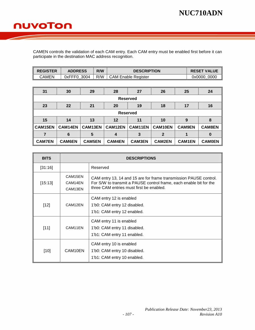
NUC710ADN
Publication Release Date: November23, 2013 - 107 - Revision A10
CAMEN controls the validation of each CAM entry. Each CAM entry must be enabled first before it can participate in the destination MAC address recognition.
REGISTER ADDRESS R/W DESCRIPTION RESET VALUE CAMEN 0xFFF0_3004 R/W CAM Enable Register 0x0000_0000
31 30 29 28 27 26 25 24 Reserved
23 22 21 20 19 18 17 16 Reserved
15 14 13 12 11 10 9 8 CAM15EN CAM14EN CAM13EN CAM12EN CAM11EN CAM10EN CAM9EN CAM8EN
7 6 5 4 3 2 1 0 CAM7EN CAM6EN CAM5EN CAM4EN CAM3EN CAM2EN CAM1EN CAM0EN
BITS DESCRIPTIONS
[31:16] Reserved
[15:13] CAM15EN
CAM14EN
CAM13EN
CAM entry 13, 14 and 15 are for frame transmission PAUSE control. For S/W to transmit a PAUSE control frame, each enable bit for the three CAM entries must first be enabled.
[12] CAM12EN CAM entry 12 is enabled 1’b0: CAM entry 12 disabled. 1’b1: CAM entry 12 enabled.
[11] CAM11EN CAM entry 11 is enabled 1’b0: CAM entry 11 disabled. 1’b1: CAM entry 11 enabled.
[10] CAM10EN CAM entry 10 is enabled 1’b0: CAM entry 10 disabled. 1’b1: CAM entry 10 enabled.
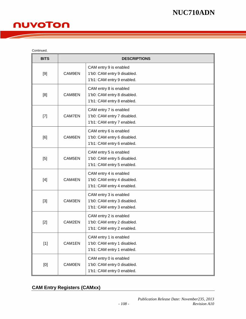
NUC710ADN
Publication Release Date: November235, 2013 - 108 - Revision A10
Continued.
BITS DESCRIPTIONS
[9] CAM9EN CAM entry 9 is enabled 1’b0: CAM entry 9 disabled. 1’b1: CAM entry 9 enabled.
[8] CAM8EN CAM entry 8 is enabled 1’b0: CAM entry 8 disabled. 1’b1: CAM entry 8 enabled.
[7] CAM7EN CAM entry 7 is enabled 1’b0: CAM entry 7 disabled. 1’b1: CAM entry 7 enabled.
[6] CAM6EN CAM entry 6 is enabled 1’b0: CAM entry 6 disabled. 1’b1: CAM entry 6 enabled.
[5] CAM5EN CAM entry 5 is enabled 1’b0: CAM entry 5 disabled. 1’b1: CAM entry 5 enabled.
[4] CAM4EN CAM entry 4 is enabled 1’b0: CAM entry 4 disabled. 1’b1: CAM entry 4 enabled.
[3] CAM3EN CAM entry 3 is enabled 1’b0: CAM entry 3 disabled. 1’b1: CAM entry 3 enabled.
[2] CAM2EN CAM entry 2 is enabled 1’b0: CAM entry 2 disabled. 1’b1: CAM entry 2 enabled.
[1] CAM1EN CAM entry 1 is enabled 1’b0: CAM entry 1 disabled. 1’b1: CAM entry 1 enabled.
[0] CAM0EN CAM entry 0 is enabled 1’b0: CAM entry 0 disabled. 1’b1: CAM entry 0 enabled.
CAM Entry Registers (CAMxx)
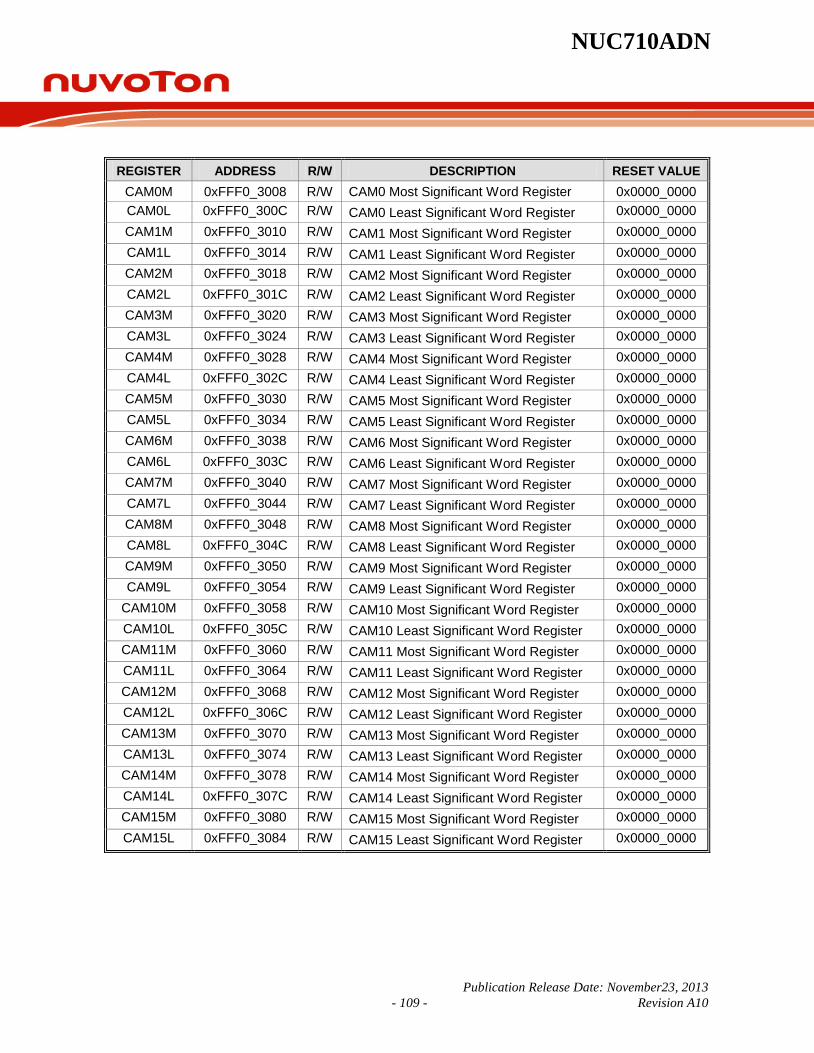
NUC710ADN
Publication Release Date: November23, 2013 - 109 - Revision A10
REGISTER ADDRESS R/W DESCRIPTION RESET VALUE CAM0M 0xFFF0_3008 R/W CAM0 Most Significant Word Register 0x0000_0000 CAM0L 0xFFF0_300C R/W CAM0 Least Significant Word Register 0x0000_0000 CAM1M 0xFFF0_3010 R/W CAM1 Most Significant Word Register 0x0000_0000 CAM1L 0xFFF0_3014 R/W CAM1 Least Significant Word Register 0x0000_0000 CAM2M 0xFFF0_3018 R/W CAM2 Most Significant Word Register 0x0000_0000 CAM2L 0xFFF0_301C R/W CAM2 Least Significant Word Register 0x0000_0000 CAM3M 0xFFF0_3020 R/W CAM3 Most Significant Word Register 0x0000_0000 CAM3L 0xFFF0_3024 R/W CAM3 Least Significant Word Register 0x0000_0000 CAM4M 0xFFF0_3028 R/W CAM4 Most Significant Word Register 0x0000_0000 CAM4L 0xFFF0_302C R/W CAM4 Least Significant Word Register 0x0000_0000 CAM5M 0xFFF0_3030 R/W CAM5 Most Significant Word Register 0x0000_0000 CAM5L 0xFFF0_3034 R/W CAM5 Least Significant Word Register 0x0000_0000 CAM6M 0xFFF0_3038 R/W CAM6 Most Significant Word Register 0x0000_0000 CAM6L 0xFFF0_303C R/W CAM6 Least Significant Word Register 0x0000_0000 CAM7M 0xFFF0_3040 R/W CAM7 Most Significant Word Register 0x0000_0000 CAM7L 0xFFF0_3044 R/W CAM7 Least Significant Word Register 0x0000_0000 CAM8M 0xFFF0_3048 R/W CAM8 Most Significant Word Register 0x0000_0000 CAM8L 0xFFF0_304C R/W CAM8 Least Significant Word Register 0x0000_0000 CAM9M 0xFFF0_3050 R/W CAM9 Most Significant Word Register 0x0000_0000 CAM9L 0xFFF0_3054 R/W CAM9 Least Significant Word Register 0x0000_0000
CAM10M 0xFFF0_3058 R/W CAM10 Most Significant Word Register 0x0000_0000 CAM10L 0xFFF0_305C R/W CAM10 Least Significant Word Register 0x0000_0000 CAM11M 0xFFF0_3060 R/W CAM11 Most Significant Word Register 0x0000_0000 CAM11L 0xFFF0_3064 R/W CAM11 Least Significant Word Register 0x0000_0000 CAM12M 0xFFF0_3068 R/W CAM12 Most Significant Word Register 0x0000_0000 CAM12L 0xFFF0_306C R/W CAM12 Least Significant Word Register 0x0000_0000 CAM13M 0xFFF0_3070 R/W CAM13 Most Significant Word Register 0x0000_0000 CAM13L 0xFFF0_3074 R/W CAM13 Least Significant Word Register 0x0000_0000 CAM14M 0xFFF0_3078 R/W CAM14 Most Significant Word Register 0x0000_0000 CAM14L 0xFFF0_307C R/W CAM14 Least Significant Word Register 0x0000_0000 CAM15M 0xFFF0_3080 R/W CAM15 Most Significant Word Register 0x0000_0000 CAM15L 0xFFF0_3084 R/W CAM15 Least Significant Word Register 0x0000_0000

NUC710ADN
Publication Release Date: November235, 2013 - 110 - Revision A10
CAMxM
31 30 29 28 27 26 25 24 MAC Address Byte 5 (MSB)
23 22 21 20 19 18 17 16 MAC Address Byte 4
15 14 13 12 11 10 9 8 MAC Address Byte 3
7 6 5 4 3 2 1 0 MAC Address Byte 2
BITS DESCRIPTIONS
[31:0] CAMxM
CAMxM (CAMx Most Significant Word) stores bits 47~16 of the MAC address. The x can be 0~14. The register pair CAMxM, CAMxL represents a CAM entry and can store a MAC address. For example, if the MAC address 00-50-BA-33-BA-44 is kept in CAM entry 1, the register CAM1M is 32’h0050_BA33 and CAM1L is 32’hBA44_0000.
CAMxL
31 30 29 28 27 26 25 24 MAC Address Byte 1
23 22 21 20 19 18 17 16 MAC Address Byte 0 (LSB)
15 14 13 12 11 10 9 8 Reserved
7 6 5 4 3 2 1 0 Reserved
BITS DESCRIPTIONS
[31:16] CAMxL
CAMxL(CAMx Least Significant Word) stores the bit 15~0 of MAC address. The x can be the 0~14. The register pair CAMxM, CAMxL represents a CAM entry and can store a MAC address. For example, if the MAC address 00-50-BA-33-BA-44 is kept in CAM entry 1, the register CAM1M is 32’h0050_BA33 and CAM1L is 32’hBA44_0000.
[15:0] Reserved -
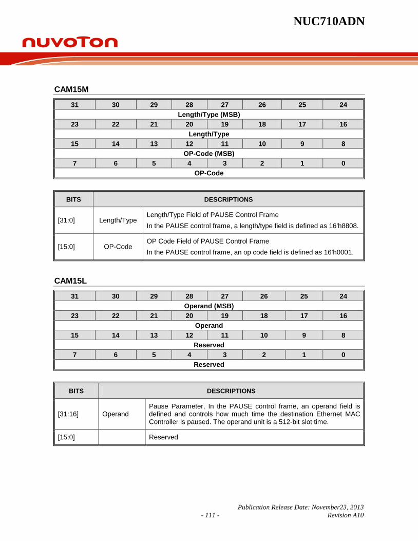
NUC710ADN
Publication Release Date: November23, 2013 - 111 - Revision A10
CAM15M
31 30 29 28 27 26 25 24 Length/Type (MSB)
23 22 21 20 19 18 17 16 Length/Type
15 14 13 12 11 10 9 8 OP-Code (MSB)
7 6 5 4 3 2 1 0 OP-Code
BITS DESCRIPTIONS
[31:0] Length/Type Length/Type Field of PAUSE Control Frame In the PAUSE control frame, a length/type field is defined as 16’h8808.
[15:0] OP-Code OP Code Field of PAUSE Control Frame In the PAUSE control frame, an op code field is defined as 16’h0001.
CAM15L
31 30 29 28 27 26 25 24 Operand (MSB)
23 22 21 20 19 18 17 16 Operand
15 14 13 12 11 10 9 8 Reserved
7 6 5 4 3 2 1 0 Reserved
BITS DESCRIPTIONS
[31:16] Operand Pause Parameter, In the PAUSE control frame, an operand field is defined and controls how much time the destination Ethernet MAC Controller is paused. The operand unit is a 512-bit slot time.
[15:0] Reserved
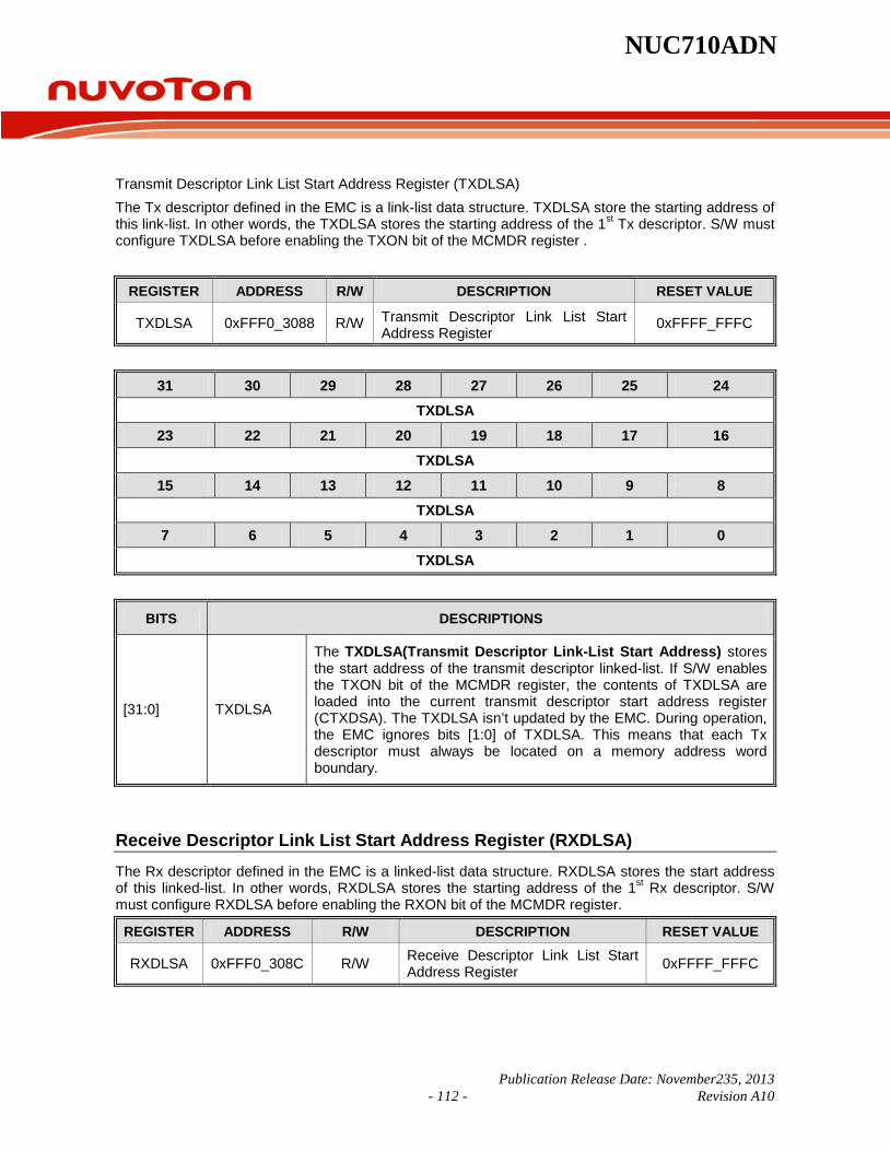
NUC710ADN
Publication Release Date: November235, 2013 - 112 - Revision A10
Transmit Descriptor Link List Start Address Register (TXDLSA) The Tx descriptor defined in the EMC is a link-list data structure. TXDLSA store the starting address of this link-list. In other words, the TXDLSA stores the starting address of the 1st Tx descriptor. S/W must configure TXDLSA before enabling the TXON bit of the MCMDR register .
REGISTER ADDRESS R/W DESCRIPTION RESET VALUE
TXDLSA 0xFFF0_3088 R/W Transmit Descriptor Link List Start Address Register
0xFFFF_FFFC
31 30 29 28 27 26 25 24 TXDLSA
23 22 21 20 19 18 17 16 TXDLSA
15 14 13 12 11 10 9 8 TXDLSA
7 6 5 4 3 2 1 0 TXDLSA
BITS DESCRIPTIONS
[31:0] TXDLSA
The TXDLSA(Transmit Descriptor Link-List Start Address) stores the start address of the transmit descriptor linked-list. If S/W enables the TXON bit of the MCMDR register, the contents of TXDLSA are loaded into the current transmit descriptor start address register (CTXDSA). The TXDLSA isn’t updated by the EMC. During operation, the EMC ignores bits [1:0] of TXDLSA. This means that each Tx descriptor must always be located on a memory address word boundary.
Receive Descriptor Link List Start Address Register (RXDLSA) The Rx descriptor defined in the EMC is a linked-list data structure. RXDLSA stores the start address of this linked-list. In other words, RXDLSA stores the starting address of the 1st Rx descriptor. S/W must configure RXDLSA before enabling the RXON bit of the MCMDR register.
REGISTER ADDRESS R/W DESCRIPTION RESET VALUE
RXDLSA 0xFFF0_308C R/W Receive Descriptor Link List Start Address Register 0xFFFF_FFFC
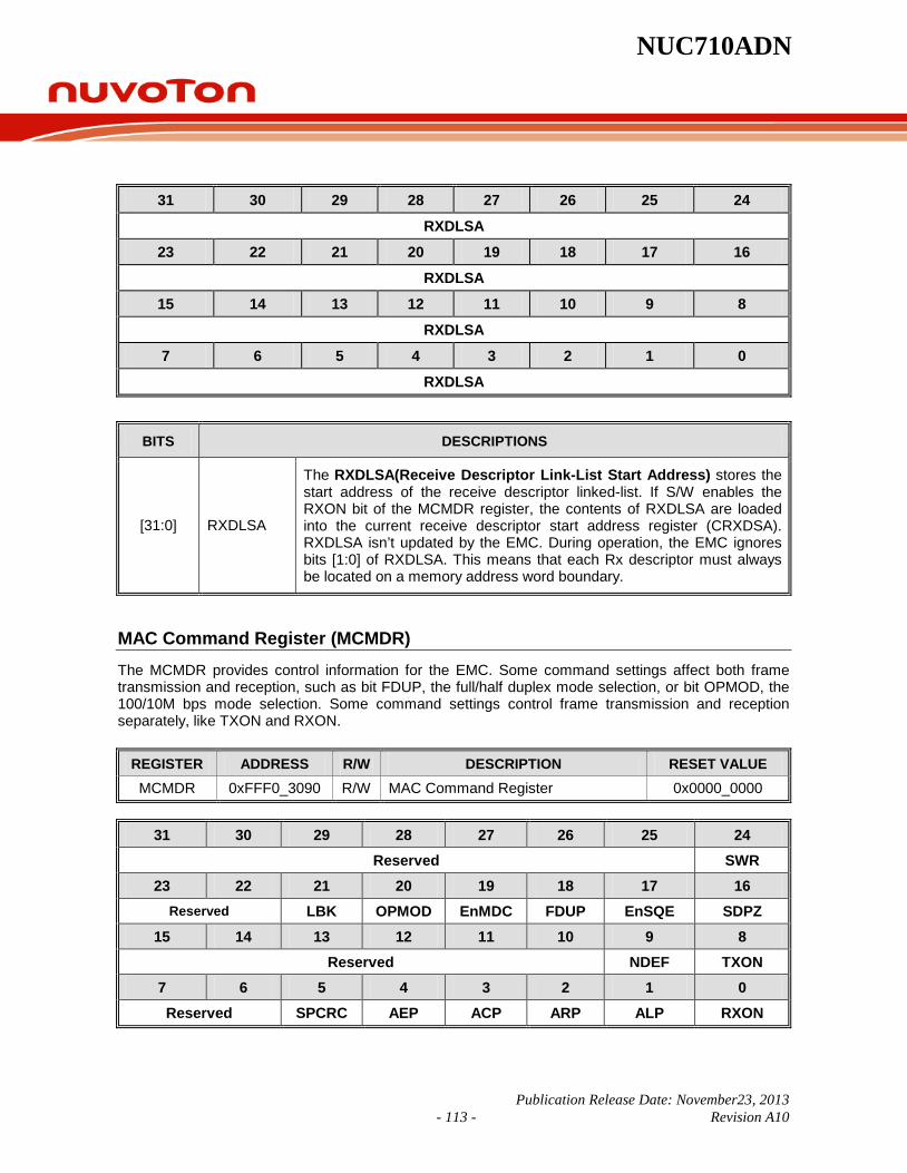
NUC710ADN
Publication Release Date: November23, 2013 - 113 - Revision A10
31 30 29 28 27 26 25 24
RXDLSA
23 22 21 20 19 18 17 16
RXDLSA
15 14 13 12 11 10 9 8
RXDLSA
7 6 5 4 3 2 1 0
RXDLSA
BITS DESCRIPTIONS
[31:0] RXDLSA
The RXDLSA(Receive Descriptor Link-List Start Address) stores the start address of the receive descriptor linked-list. If S/W enables the RXON bit of the MCMDR register, the contents of RXDLSA are loaded into the current receive descriptor start address register (CRXDSA). RXDLSA isn’t updated by the EMC. During operation, the EMC ignores bits [1:0] of RXDLSA. This means that each Rx descriptor must always be located on a memory address word boundary.
MAC Command Register (MCMDR) The MCMDR provides control information for the EMC. Some command settings affect both frame transmission and reception, such as bit FDUP, the full/half duplex mode selection, or bit OPMOD, the 100/10M bps mode selection. Some command settings control frame transmission and reception separately, like TXON and RXON.
REGISTER ADDRESS R/W DESCRIPTION RESET VALUE MCMDR 0xFFF0_3090 R/W MAC Command Register 0x0000_0000
31 30 29 28 27 26 25 24 Reserved SWR
23 22 21 20 19 18 17 16 Reserved LBK OPMOD EnMDC FDUP EnSQE SDPZ
15 14 13 12 11 10 9 8 Reserved NDEF TXON
7 6 5 4 3 2 1 0 Reserved SPCRC AEP ACP ARP ALP RXON
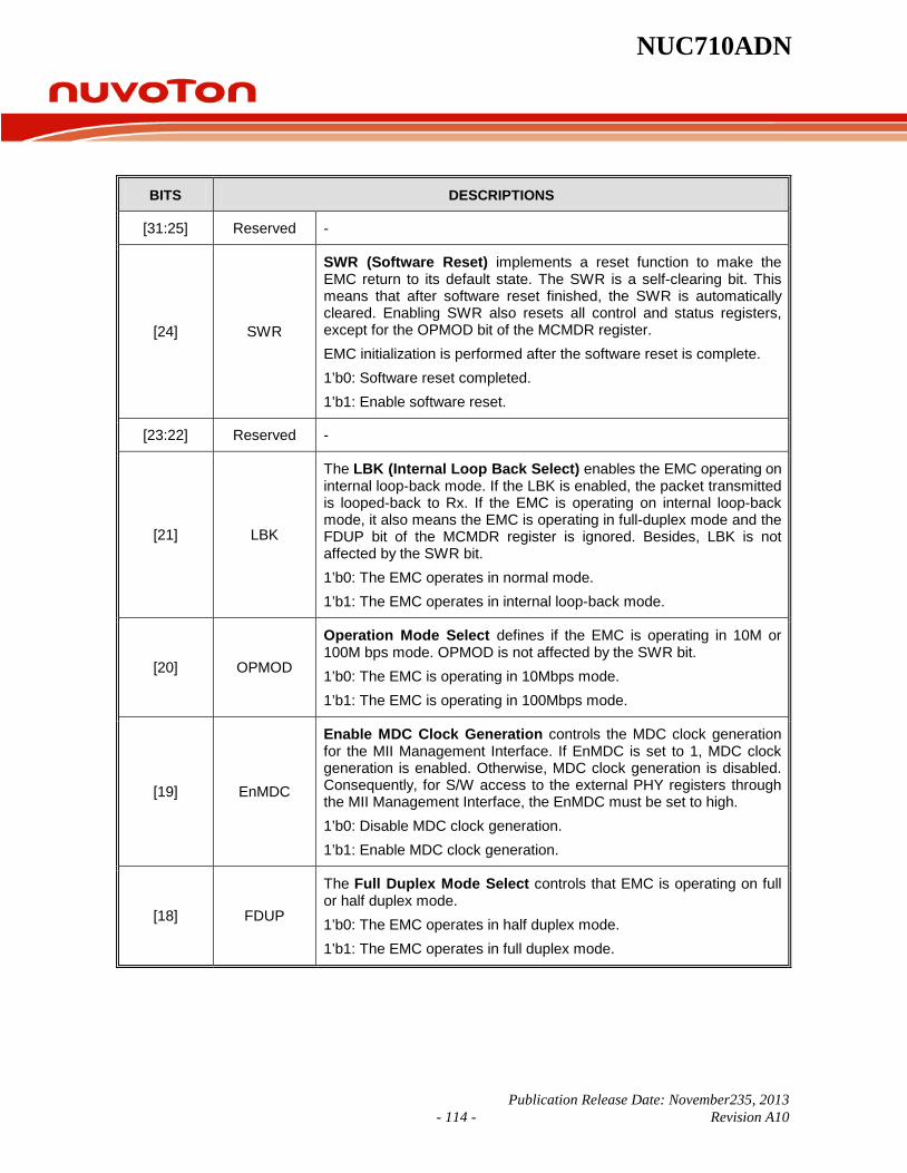
NUC710ADN
Publication Release Date: November235, 2013 - 114 - Revision A10
BITS DESCRIPTIONS
[31:25] Reserved -
[24] SWR
SWR (Software Reset) implements a reset function to make the EMC return to its default state. The SWR is a self-clearing bit. This means that after software reset finished, the SWR is automatically cleared. Enabling SWR also resets all control and status registers, except for the OPMOD bit of the MCMDR register. EMC initialization is performed after the software reset is complete. 1’b0: Software reset completed. 1’b1: Enable software reset.
[23:22] Reserved -
[21] LBK
The LBK (Internal Loop Back Select) enables the EMC operating on internal loop-back mode. If the LBK is enabled, the packet transmitted is looped-back to Rx. If the EMC is operating on internal loop-back mode, it also means the EMC is operating in full-duplex mode and the FDUP bit of the MCMDR register is ignored. Besides, LBK is not affected by the SWR bit. 1’b0: The EMC operates in normal mode. 1’b1: The EMC operates in internal loop-back mode.
[20] OPMOD
Operation Mode Select defines if the EMC is operating in 10M or 100M bps mode. OPMOD is not affected by the SWR bit. 1’b0: The EMC is operating in 10Mbps mode. 1’b1: The EMC is operating in 100Mbps mode.
[19] EnMDC
Enable MDC Clock Generation controls the MDC clock generation for the MII Management Interface. If EnMDC is set to 1, MDC clock generation is enabled. Otherwise, MDC clock generation is disabled. Consequently, for S/W access to the external PHY registers through the MII Management Interface, the EnMDC must be set to high. 1’b0: Disable MDC clock generation. 1’b1: Enable MDC clock generation.
[18] FDUP
The Full Duplex Mode Select controls that EMC is operating on full or half duplex mode. 1’b0: The EMC operates in half duplex mode. 1’b1: The EMC operates in full duplex mode.
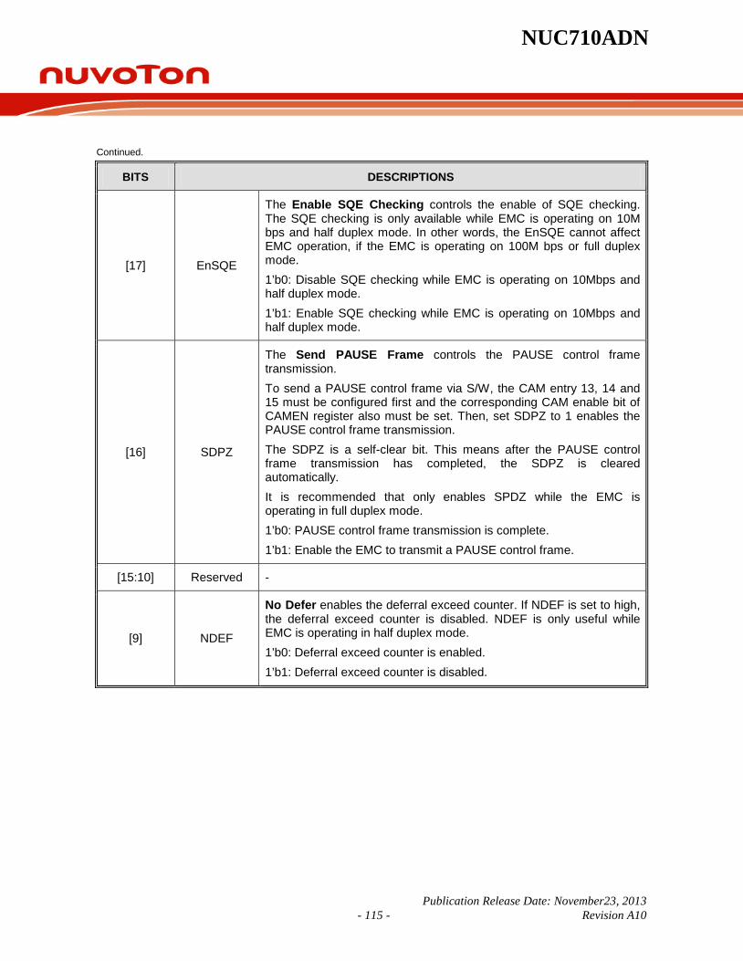
NUC710ADN
Publication Release Date: November23, 2013 - 115 - Revision A10
Continued.
BITS DESCRIPTIONS
[17] EnSQE
The Enable SQE Checking controls the enable of SQE checking. The SQE checking is only available while EMC is operating on 10M bps and half duplex mode. In other words, the EnSQE cannot affect EMC operation, if the EMC is operating on 100M bps or full duplex mode. 1’b0: Disable SQE checking while EMC is operating on 10Mbps and half duplex mode. 1’b1: Enable SQE checking while EMC is operating on 10Mbps and half duplex mode.
[16] SDPZ
The Send PAUSE Frame controls the PAUSE control frame transmission. To send a PAUSE control frame via S/W, the CAM entry 13, 14 and 15 must be configured first and the corresponding CAM enable bit of CAMEN register also must be set. Then, set SDPZ to 1 enables the PAUSE control frame transmission. The SDPZ is a self-clear bit. This means after the PAUSE control frame transmission has completed, the SDPZ is cleared automatically. It is recommended that only enables SPDZ while the EMC is operating in full duplex mode. 1’b0: PAUSE control frame transmission is complete. 1’b1: Enable the EMC to transmit a PAUSE control frame.
[15:10] Reserved -
[9] NDEF
No Defer enables the deferral exceed counter. If NDEF is set to high, the deferral exceed counter is disabled. NDEF is only useful while EMC is operating in half duplex mode. 1’b0: Deferral exceed counter is enabled. 1’b1: Deferral exceed counter is disabled.
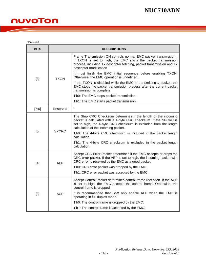
NUC710ADN
Publication Release Date: November235, 2013 - 116 - Revision A10
Continued.
BITS DESCRIPTIONS
[8] TXON
Frame Transmission ON controls normal EMC packet transmission . If TXON is set to high, the EMC starts the packet transmission process, including Tx descriptor fetching, packet transmission and Tx descriptor modification. It must finish the EMC initial sequence before enabling TXON. Otherwise, the EMC operation is undefined. If the TXON is disabled while the EMC is transmitting a packet, the EMC stops the packet transmission process after the current packet transmission is complete. 1’b0: The EMC stops packet transmission. 1’b1: The EMC starts packet transmission.
[7:6] Reserved -
[5] SPCRC
The Strip CRC Checksum determines if the length of the incoming packet is calculated with a 4-byte CRC checksum. If the SPCRC is set to high, the 4-byte CRC checksum is excluded from the length calculation of the incoming packet. 1’b0: The 4-byte CRC checksum is included in the packet length calculation. 1’b1: The 4-byte CRC checksum is excluded in the packet length calculation.
[4] AEP
Accept CRC Error Packet determines if the EMC accepts or drops the CRC error packet. If the AEP is set to high, the incoming packet with CRC error is received by the EMC as a good packet. 1’b0: CRC error packet was dropped by the EMC. 1’b1: CRC error packet was accepted by the EMC.
[3] ACP
Accept Control Packet determines control frame reception. If the ACP is set to high, the EMC accepts the control frame. Otherwise, the control frame is dropped. It is recommended that S/W only enable AEP when the EMC is operating in full duplex mode. 1’b0: The control frame is dropped by the EMC. 1’b1: The control frame is accepted by the EMC.

NUC710ADN
Publication Release Date: November23, 2013 - 117 - Revision A10
Continued.
BITS DESCRIPTIONS
[2] ARP
Accept Runt Packet controls runt packet (packets containing less than 64 bytes) reception. If the ARP is set to high, the EMC will accept the runt packet. Otherwise, the runt packet is dropped. 1’b0: Runt packet was dropped by EMC. 1’b1: Runt packet was accepted by EMC.
[1] ALP
Accept Long Packet determines long packets (packets containing more than 1518 bytes) reception. If the ALP is set to high, the EMC accepts the long packet. Otherwise, the long packet is dropped. 1’b0: The long packet was dropped by the EMC. 1’b1: The long packet was accepted by the EMC.
[0] RXON
Frame Reception ON controls the EMC normal packet reception. If RXON is set to high, the EMC starts the packet reception process, including fetching the Rx descriptor, packet reception and Rx descriptor modification. It the EMC initial sequence must finish before enabling RXON. Otherwise, the EMC operation is undefined. If RXON is disabled while the EMC is receiving an incoming packet, the EMC stops the packet reception process after the current packet reception is complete. 1’b0: The EMC stops the packet reception process. 1’b1: The EMC starts the packet reception process.
MII Management Data Register (MIID) The EMC provides the MII management function to access the control and status registers of the external PHY. The MIID register is used to store the data to be written into the registers of external PHY for write commands or the data that is read from the registers of external PHY for read commands.
REGISTER ADDRESS R/W DESCRIPTION RESET VALUE MIID 0xFFF0_3094 R/W MII Management Data Register 0x0000_0000

NUC710ADN
Publication Release Date: November235, 2013 - 118 - Revision A10
31 30 29 28 27 26 25 24 Reserved
23 22 21 20 19 18 17 16 Reserved
15 14 13 12 11 10 9 8 MIIData
7 6 5 4 3 2 1 0 MIIData
BITS DESCRIPTIONS
[31:16] Reserved -
[15:0] MIIData
MII Management Data is the 16-bit data that is written to the registers of external PHY for MII Management write command or the data from the registers of external PHY for MII Management read command.
MII Management Control and Address Register (MIIDA) The EMC provides an MII management function to access the control and status registers of the external PHY. The MIIDA register is used to store the MII management command information, like the register address, external PHY address, MDC clocking rate, read/write etc.
REGISTER ADDRESS R/W DESCRIPTION RESET VALUE
MIIDA 0xFFF0_3098 R/W MII Management Control and Address Register 0x0090_0000
31 30 29 28 27 26 25 24 Reserved
23 22 21 20 19 18 17 16 MDCCR MDCON PreSP BUSY Write
15 14 13 12 11 10 9 8 Reserved PHYAD
7 6 5 4 3 2 1 0 Reserved PHYRAD
BITS DESCRIPTIONS

NUC710ADN
Publication Release Date: November23, 2013 - 119 - Revision A10
[31:24] Reserved -
[23:20] MDCCR
The MDC Clock Rating controls the MDC clock rating for MII Management I/F. Depending on the IEEE Std. 802.3 clause 22.2.2.11, the minimum period for the MDC shall be 400ns. In other words, the maximum frequency for the MDC is 2.5MHz. The MDC is divided from the AHB bus clock, the HCLK. Consequently, for different HCLKs the different ratios are required to generate an appropriate MDC clock. The following table shows the relationship between the HCLK and MDC clocks in different MDCCR configurations. The THCLK indicates the HCLK period.
[19] MDC
The MDC Clock ON Always controls the MDC clock generation. If the MDCON is set to high, the MDC clock is always active. Otherwise, the MDC only activates while the S/W issues an MII management command. 1’b0: The MDC clock is only active while the S/W issues a MII management command. 1’b1: The MDC clock is always active.
[18] PreSP
Preamble Suppress controls the preamble field generation of the MII management frame. If the PreSP is set to high, the preamble field generation of the MII management frame is skipped. 1’b0: Preamble field generation of the MII management frame is not skipped. 1’b1: Preamble field generation of the MII management frame is skipped.
[17] BUSY
The Busy Bit enables MII management frame generation. For S/W access to the external PHY registers, the BUSY bit must be set high, and the EMC generates the MII management frame external PHY through MII Management I/F. The BUSY bit is self-clearing. This means the BUSY is cleared automatically after the MII management command finishes. 1’b0: The MII management has finished. 1’b1: Enable EMC generation of an MII management command to external PHY.
[16] Write
The Write Command defines if the MII management command is read or write. 1’b0: MII management command is a read command. 1’b1: MII management command is a write command.
[15:13] Reserved
Continued.
BITS DESCRIPTIONS

NUC710ADN
Publication Release Date: November235, 2013 - 120 - Revision A10
[12:8] PHYAD The PHY Address stores the address to differentiate which external PHY is the target of the MII management command.
[7:5] Reserved -
[4:0] PHYRAD The PHY Register Address stores the address to indicate which register of the external PHY is the target of the MII management command.
MDCCR [23:20] MDC CLOCK PERIOD MDC CLOCK FREQUENCY
4’b0000 4 x THCLK HCLK/4
4’b0001 6 x THCLK HCLK/6
4’b0010 8 x THCLK HCLK/8
4’b0011 12 x THCLK HCLK/12
4’b0100 16 x THCLK HCLK/16
4’b0101 20 x THCLK HCLK/20
4’b0110 24 x THCLK HCLK/24
4’b0111 28 x THCLK HCLK/28
4’b1000 30 x THCLK HCLK/30
4’b1001 32 x THCLK HCLK/32
4’b1010 36 x THCLK HCLK/36
4’b1011 40 x THCLK HCLK/40
4’b1100 44 x THCLK HCLK/44
4’b1101 48 x THCLK HCLK/48
4’b1110 54 x THCLK HCLK/54
4’b1111 60 x THCLK HCLK/60
MII Management Function Frame Format IEEE Std. 802.3 clause 22.2.4 defines the MII management function. The MII management function is used for the purpose of controlling the PHY and obtaining the status of the PHY. The MII management frame format is shown as follows.

NUC710ADN
Publication Release Date: November23, 2013 - 121 - Revision A10
Management frame fields
PRE ST OP PHYAD REGAD TA DATA IDLE READ 1…1 01 10 AAAAA RRRRR Z0 DDDDDDDDDDDDDDDD Z WRITE 1…1 01 01 AAAAA RRRRR 10 DDDDDDDDDDDDDDDD Z
MII Management Function Configure Sequence
READ WRITE
1. Set appropriate MDCCR. 2. Set PHYAD and PHYRAD. 3. Set Write to 1’b0 4. Set bit BUSY to 1’b1 to send a MII
management frame out. 5. Wait BUSY to become 1’b0. 6. Read data from MIID register. 7. Finish the read command.
1. Write data to MIID register 2. Set appropriate MDCCR. 3. Set PHYAD and PHYRAD. 4. Set Write to 1’b1 5. Set bit BUSY to 1’b1 to send a MII
management frame out. 6. Wait BUSY to become 1’b0. 7. Finish the write command.
FIFO Threshold Control Register (FFTCR) FFTCR defines the high and low threshold of internal FIFOs, including TxFIFO and RxFIFO. The threshold of internal FIFOs is related to EMC request generation and when the frame transmission starts. FFTCR also defines the burst length of AHB bus cycle for system memory access.
REGISTER ADDRESS R/W DESCRIPTION RESET VALUE FFTCR 0xFFF0_309C R/W FIFO Threshold Control Register 0x0000_0101
31 30 29 28 27 26 25 24 Reserved
23 22 21 20 19 18 17 16 Reserved BLength Reserved
15 14 13 12 11 10 9 8 Reserved TxTHD
7 6 5 4 3 2 1 0 Reserved RxTHD

NUC710ADN
Publication Release Date: November235, 2013 - 122 - Revision A10
BITS DESCRIPTIONS
[31:22] Reserved -
[21:20] Blength
DMA Burst Length defines the burst length of the AHB bus cycle while the EMC accesses system memory. 2’b00: 4 words 2’b01: 8 words 2’b10: 16 words 2’b11: 16 words
[19:10] Reserved -
[9:8] TxTHD
TxFIFO Low Threshold controls when TxDMA requests internal arbiter for data transfer between system memory and TxFIFO. The TxTHD defines not only the low threshold of TxFIFO, but also the high threshold. The high threshold is always twice the low threshold. During packet transmission, if TxFIFO reaches the high threshold, the TxDMA stops generating requests to transfer frame data from system memory to TxFIFO. If the frame data in TxFIFO is less than the low threshold, TxDMA starts to transfer frame data from system memory to TxFIFO. The TxTHD also defines when the TxMAC starts to transmit frame. The TxMAC starts to transmit the frame while the TxFIFO first time reaches the high threshold during the transmission. If the frame data length is less than the TxFIFO high threshold, the TxMAC transmits the frame only after all the frame data are inside the TxFIFO. 2’b00: Undefined. 2’b01: TxFIFO low threshold is 64B and high threshold is 128B. 2’b10: TxFIFO low threshold is 80B and high threshold is 160B. 2’b11: TxFIFO low threshold is 96B and high threshold is 192B.
[7:2] Reserved
[1:0] RxTHD
RxFIFO High Threshold controls when RxDMA requests the internal arbiter for data transfer between RxFIFO and system memory. The RxTHD defines not only the high threshold of RxFIFO, but also the low threshold. The low threshold is always half of the high threshold. During packet reception, if the RxFIFO reaches the high threshold, the RxDMA starts to transfer frame data from RxFIFO to system memory. If the frame data in RxFIFO is less than the low threshold, RxDMA stops transferring the frame data to system memory. 2’b00: Depending on the burst length setting. If the burst length is 8 words, the high threshold is also 8 words. 2’b01: RxFIFO high threshold is 64B and low threshold is 32B. 2’b10: RxFIFO high threshold is 128B and low threshold is 64B. 2’b11: RxFIFO high threshold is 192B and low threshold is 96B.

NUC710ADN
Publication Release Date: November23, 2013 - 123 - Revision A10
Transmit Start Demand Register (TSDR) While the Tx descriptor is unavailable for use of TxDMA after TXON of the MCMDR register is enabled, the FSM (Finite State Machine) of TxDMA enters the Halt state, and the frame transmission is halted. After the S/W has prepared the new Tx descriptor for frame transmission, it must issue a write command to TSDR register to make TxDMA exit the Halt state and continue frame transmission. TSDR is a write only register, and reading from this register is undefined. The write to TSDR register only takes effect while TxDMA is in the Halt state.
REGISTER ADDRESS R/W DESCRIPTION RESET VALUE TSDR 0xFFF0_30A0 W Transmit Start Demand Register Undefined
BITS DESCRIPTIONS
[31:0] Reserved -
Receive Start Demand Register (RSDR) If the RxDMA Rx descriptor is not available for use after RXON of the MCMDR register is enabled, the FSM (Finite State Machine) of RxDMA enters the Halt state and frame reception is halted. After S/W has prepared the new Rx descriptor for frame reception, it must issue a write command to the RSDR register to make RxDMA exit the Halt state and continue frame reception. The RSDR is a write only register and read from this register is undefined. The RSDR register write only takes affect when RxDMA is in the Halt state.
REGISTER ADDRESS R/W DESCRIPTION RESET VALUE RSDR 0xFFF0_30A4 W Receive Start Demand Register Undefined
BITS DESCRIPTIONS
[31:0] Reserved --
Maximum Receive Frame Control Register (DMARFC) The DMARFC defines the maximum frame length for a received frame that can be stored in system memory. It is recommend to only use this register for receiving frame lengths greater than 1518 bytes.
REGISTER ADDRESS R/W DESCRIPTION RESET VALUE
DMARFC 0xFFF0_30A8 R/W Maximum Receive Frame Control Register 0x0000_0800

NUC710ADN
Publication Release Date: November235, 2013 - 124 - Revision A10
31 30 29 28 27 26 25 24
Reserved 23 22 21 20 19 18 17 16
Reserved 15 14 13 12 11 10 9 8
RXMS 7 6 5 4 3 2 1 0
RXMS
BITS DESCRIPTIONS
[31:16] Reserved -
[15:0] RXMS
The Maximum Receive Frame Length defines the maximum frame length for received frames. If the frame length of the received frame is greater than the RXMS, and the EnDFO bit of the MIEN register is also enabled, the DFOI bit of the MISTA register is set and the Rx interrupt is triggered. It is recommended to only use RXMS to qualify the length of a received frame for S/W to receive a frame of length greater than 1518 bytes.
MAC Interrupt Enable Register (MIEN) The MIEN controls the enable of EMC interrupt status to generate interrupt. Two interrupts, RXINTR for frame reception and TXINTR for frame transmission, are generated from EMC to CPU.
REGISTER ADDRESS R/W DESCRIPTION RESET VALUE MIEN 0xFFF0_30AC R/W MAC Interrupt Enable Register 0x0000_0000
31 30 29 28 27 26 25 24 Reserved EnTxBErr
23 22 21 20 19 18 17 16 EnTDU EnLC EnTXABT EnNCS EnEXDEF EnTXCP EnTXEMP EnTXINTR
15 14 13 12 11 10 9 8 Reserved EnCFR Reserved EnRxBErr EnRDU EnDEN EnDFO
7 6 5 4 3 2 1 0 EnMMP EnRP EnALIE EnRXGD EnPTLE EnRXOV EnCRCE EnRXINTR

NUC710ADN
Publication Release Date: November23, 2013 - 125 - Revision A10
BITS DESCRIPTIONS
[31:25] Reserved -
[24] EnTxBErr
Enable Transmit Bus Error Interrupt controls the TxBErr interrupt generation. If TxBErr of MISTA register is set, and both EnTxBErr and EnTXINTR are enabled, the EMC generates the Tx CPU interrupt. If EnTxBErr or EnTXINTR is disabled, no Tx CPU interrupt is generated even if the TxBErr of MISTA register is set. 1’b0: TxBErr of MISTA register is masked from Tx interrupt generation. 1’b1: TxBErr of MISTA register can participate in Tx interrupt generation.
[23] EnTDU
Enable Transmit Descriptor Unavailable Interrupt controls the TDU interrupt generation. If TDU of MISTA register is set, and both EnTDU and EnTXINTR are enabled, the EMC generates the Tx CPU interrupt. If EnTDU or EnTXINTR is disabled, no Tx CPU interrupt is generated even if the TDU of MISTA register is set. 1’b0: TDU of MISTA register is masked from Tx interrupt generation. 1’b1: TDU of MISTA register can participate in Tx interrupt generation.
[22] EnLC
Enable Late Collision Interrupt controls the LC interrupt generation. If LC of MISTA register is set, and both EnLC and EnTXINTR are enabled, the EMC generates the Tx CPU interrupt . If EnLC or EnTXINTR is disabled, no Tx interrupt is generated even if the LC of MISTA register is set. 1’b0: LC of MISTA register is masked from Tx interrupt generation. 1’b1: LC of MISTA register can participate in Tx interrupt generation.
[21] EnTXABT
Enable Transmit Abort Interrupt controls the TXABT interrupt generation. If TXABT of the MISTA register is set, and both EnTXABT and EnTXINTR are enabled, the EMC generates the Tx CPU interrupt . If EnTXABT or EnTXINTR is disabled, no Tx CPU interrupt is generated, even if the TXABT of MISTA register is set. 1’b0: TXABT of MISTA register is masked from Tx interrupt generation. 1’b1: TXABT of MISTA register can participate in Tx interrupt generation.
[20] EnNCS
Enable No Carrier Sense Interrupt controls NCS interrupt generation. If NCS of the MISTA register is set, and both EnNCS and EnTXINTR are enabled, the EMC generates the Tx CPU interrupt . If EnNCS or EnTXINTR is disabled, no Tx CPU interrupt is generated, even if the NCS of the MISTA register is set. 1’b0: NCS of MISTA register is masked from Tx interrupt generation. 1’b1: NCS of MISTA register can participate in Tx interrupt generation.

NUC710ADN
Publication Release Date: November235, 2013 - 126 - Revision A10
Continued.
BITS DESCRIPTIONS
[19] EnEXDEF
Enable Defer Exceed Interrupt controls EXDEF interrupt generation. If EXDEF of the MISTA register is set, and both EnEXDEF and EnTXINTR are enabled, the EMC generates the Tx CPU interrupt. If EnEXDEF or EnTXINTR is disabled, no Tx CPU interrupt is generated, even if the EXDEF of MISTA register is set. 1’b0: EXDEF of MISTA register is masked from Tx interrupt generation. 1’b1: EXDEF of MISTA register can participate in Tx interrupt generation.
[18] EnTXCP
The Enable Transmit Completion Interrupt controls the TXCP interrupt generation. If TXCP of MISTA register is set, and both EnTXCP and EnTXINTR are enabled, the EMC generates the Tx CPU interrupt. If EnTXCP or EnTXINTR is disabled, no Tx CPU interrupt is generated, even if the TXCP of MISTA register is set. 1’b0: TXCP of MISTA register is masked from Tx interrupt generation. 1’b1: TXCP of MISTA register can participate in Tx interrupt generation.
[17] EnTXEMP
The Enable Transmit FIFO Underflow Interrupt controls the TXEMP interrupt generation. If TXEMP of MISTA register is set, and both EnTXEMP and EnTXINTR are enabled, the EMC generates the Tx CPU interrupt. If EnTXEMP or EnTXINTR is disabled, no Tx CPU interrupt is generated, even if the TXEMP of MISTA register is set. 1’b0: TXEMP of MISTA register is masked from Tx interrupt generation. 1’b1: TXEMP of MISTA register can participate in Tx interrupt generation.
[16] EnTXINTR
The EnTXINTR controls the Tx interrupt generation. If Enable Transmit Interrupt is enabled and TXINTR of the MISTA register is high, EMC generates the Tx CPU interrupt. If EnTXINTR is disabled, no Tx CPU interrupt is generated, even if the status bits 17~24 of MISTA are set and the corresponding bits of MIEN are enabled. In other words, for S/W to receive a Tx interrupt from EMC, this bit must be enabled. And, if S/W doesn’t want to receive any Tx interrupt from EMC, disables this bit. 1’b0: TXINTR of MISTA register is masked and Tx interrupt generation is disabled. 1’b1: TXINTR of MISTA register is unmasked and Tx interrupt generation is enabled.
[15] Reserved --
[14] EnCFR
Enable Control Frame Receive Interrupt controls CFR interrupt generation. If CFR of the MISTA register is set, and both EnCFR and EnTXINTR are enabled, the EMC generates the Rx CPU interrupt. If EnCFR or EnTXINTR is disabled, no Rx CPU interrupt is generated, even if the CFR of MISTA register is set. 1’b0: CFR of MISTA register is masked from Rx interrupt generation. 1’b1: CFR of MISTA register can participate in Rx interrupt generation.

NUC710ADN
Publication Release Date: November23, 2013 - 127 - Revision A10
Continued.
BITS DESCRIPTIONS
[13:12] Reserved --
[11] EnRxBErr
The Enable Receive Bus Error Interrupt controls the RxBerr interrupt generation. If RxBErr of the MISTA register is set, and both EnRxBErr and EnTXINTR are enabled, the EMC generates the Rx CPU interrupt. If EnRxBErr or EnTXINTR is disabled, no Rx CPU interrupt is generated, even if the RxBErr of the MISTA register is set. 1’b0: RxBErr of the MISTA register is masked from Rx interrupt generation. 1’b1: RxBErr of the MISTA register can participate in Rx interrupt generation.
[10] EnRDU
Enable Receive Descriptor Unavailable Interrupt controls RDU interrupt generation. If RDU of MISTA register is set, and both EnRDU and EnTXINTR are enabled, the EMC generates the Rx CPU interrupt. If EnRDU or EnTXINTR is disabled, no Rx CPU interrupt is generated, even if the RDU of MISTA register is set. 1’b0: RDU of MISTA register is masked from Rx interrupt generation. 1’b1: RDU of MISTA register can participate in Rx interrupt generation.
[9] EnDEN
Enable DMA Early Notification Interrupt controls DENI interrupt generation. If DENI of the MISTA register is set, and both EnDEN and EnTXINTR are enabled, the EMC generates the Rx CPU interrupt. If EnDEN or EnTXINTR is disabled, no Rx CPU interrupt is generated, even if the DENI of MISTA register is set. 1’b0: DENI of MISTA register is masked from Rx interrupt generation. 1’b1: DENI of MISTA register can participate in Rx interrupt generation.
[8] EnDFO
Enable Maximum Frame Length Interrupt controls the DFOI interrupt generation. If DFOI of MISTA register is set, and both EnDFO and EnTXINTR are enabled, the EMC generates the Rx CPU interrupt. If EnDFO or EnTXINTR is disabled, no Rx CPU interrupt is generated, even if the DFOI of MISTA register is set. 1’b0: DFOI of MISTA register is masked from Rx interrupt generation. 1’b1: DFOI of MISTA register can participate in Rx interrupt generation.
[7] EnMMP
The Enable More Missed Packet Interrupt controls the MMP interrupt generation. If MMP of MISTA register is set, and both EnMMP and EnTXINTR are enabled, the EMC generates the Rx CPU interrupt. If EnMMP or EnTXINTR is disabled, no Rx CPU interrupt is generated, even if the MMP of MISTA register is set. 1’b0: MMP of MISTA register is masked from Rx interrupt generation. 1’b1: MMP of MISTA register can participate in Rx interrupt generation.

NUC710ADN
Publication Release Date: November235, 2013 - 128 - Revision A10
Continued.
BITS DESCRIPTIONS
[6] EnRP
Enable Runt Packet Interrupt controls the RP interrupt generation. If RP of MISTA register is set, and both EnRP and EnTXINTR are enabled, the EMC generates the Rx CPU interrupt. If EnRP or EnTXINTR is disabled, no Rx CPU interrupt is generated, even if the RP of MISTA register is set. 1’b0: RP of MISTA register is masked from Rx interrupt generation. 1’b1: RP of MISTA register can participate in Rx interrupt generation.
[5] EnALIE
Enable Alignment Error Interrupt controls ALIE interrupt generation. If ALIE of MISTA register is set, and both EnALIE and EnTXINTR are enabled, the EMC generates the Rx CPU interrupt. If EnALIE or EnTXINTR is disabled, no Rx CPU interrupt is generated, even if the ALIE of MISTA register is set. 1’b0: ALIE of MISTA register is masked from Rx interrupt generation. 1’b1: ALIE of MISTA register can participate in Rx interrupt generation.
[4] EnRXGD
Enable Receive Good Interrupt controls the RXGD interrupt generation. If RXGD of the MISTA register is set, and both EnRXGD and EnTXINTR are enabled, the EMC generates the Rx CPU interrupt. If EnRXGD or EnTXINTR is disabled, no Rx CPU interrupt is generated, even if the RXGD of MISTA register is set. 1’b0: RXGD of MISTA register is masked from Rx interrupt generation. 1’b1: RXGD of MISTA register can participate in Rx interrupt generation.
[3] EnPTLE
Enable Packet Too Long Interrupt controls the PTLE interrupt generation. If PTLE of MISTA register is set, and both EnPTLE and EnTXINTR are enabled, the EMC generates the Rx CPU interrupt. If EnPTLE or EnTXINTR is disabled, no Rx CPU interrupt is generated, even if the PTLE of MISTA register is set. 1’b0: PTLE of MISTA register is masked from Rx interrupt generation. 1’b1: PTLE of MISTA register can participate in Rx interrupt generation.
[2] EnRXOV
Enable Receive FIFO Overflow Interrupt controls the RXOV interrupt generation. If RXOV of MISTA register is set, and both EnRXOV and EnTXINTR are enabled, the EMC generates the Rx CPU interrupt. If EnRXOV or EnTXINTR is disabled, no Rx CPU interrupt is generated, even if the RXOV of MISTA register is set. 1’b0: RXOV of MISTA register is masked from Rx interrupt generation. 1’b1: RXOV of MISTA register can participate in Rx interrupt generation.
[1] EnCRCE
Enable CRC Error Interrupt controls the CRCE interrupt generation. If CRCE of the MISTA register is set, and both EnCRCE and EnTXINTR are enabled, the EMC generates the Rx CPU interrupt. If EnCRCE or EnTXINTR is disabled, no Rx CPU interrupt is generated, even if the CRCE of MISTA register is set. 1’b0: CRCE of MISTA register is masked from Rx interrupt generation. 1’b1: CRCE of MISTA register can participate in Rx interrupt generation.
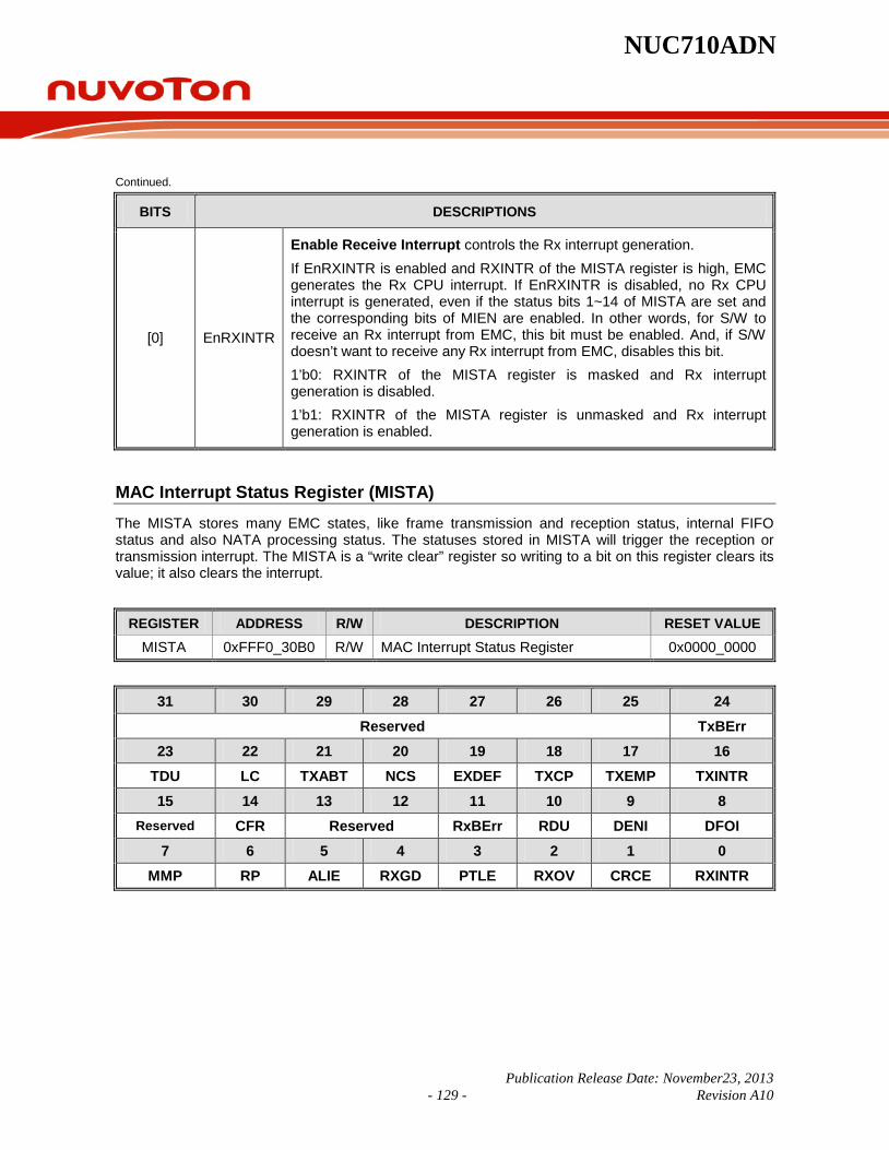
NUC710ADN
Publication Release Date: November23, 2013 - 129 - Revision A10
Continued.
BITS DESCRIPTIONS
[0] EnRXINTR
Enable Receive Interrupt controls the Rx interrupt generation. If EnRXINTR is enabled and RXINTR of the MISTA register is high, EMC generates the Rx CPU interrupt. If EnRXINTR is disabled, no Rx CPU interrupt is generated, even if the status bits 1~14 of MISTA are set and the corresponding bits of MIEN are enabled. In other words, for S/W to receive an Rx interrupt from EMC, this bit must be enabled. And, if S/W doesn’t want to receive any Rx interrupt from EMC, disables this bit. 1’b0: RXINTR of the MISTA register is masked and Rx interrupt generation is disabled. 1’b1: RXINTR of the MISTA register is unmasked and Rx interrupt generation is enabled.
MAC Interrupt Status Register (MISTA) The MISTA stores many EMC states, like frame transmission and reception status, internal FIFO status and also NATA processing status. The statuses stored in MISTA will trigger the reception or transmission interrupt. The MISTA is a “write clear” register so writing to a bit on this register clears its value; it also clears the interrupt.
REGISTER ADDRESS R/W DESCRIPTION RESET VALUE MISTA 0xFFF0_30B0 R/W MAC Interrupt Status Register 0x0000_0000
31 30 29 28 27 26 25 24 Reserved TxBErr
23 22 21 20 19 18 17 16 TDU LC TXABT NCS EXDEF TXCP TXEMP TXINTR 15 14 13 12 11 10 9 8
Reserved CFR Reserved RxBErr RDU DENI DFOI 7 6 5 4 3 2 1 0
MMP RP ALIE RXGD PTLE RXOV CRCE RXINTR

NUC710ADN
Publication Release Date: November235, 2013 - 130 - Revision A10
BITS DESCRIPTIONS
[31:25] Reserved -
[24] TxBErr
Transmit Bus Error Interrupt high is a memory controller ERROR response during EMC access to system memory through TxDMA during the packet transmission process. Resetting the EMC is recommended while the TxBErr status is high. If the TxBErr is high and EnTxBErr of the MIEN register is enabled, the TxINTR is high. Write 1 to this bit clears the TxBErr status. 1’b0: No ERROR response received. 1’b1: ERROR response received.
[23] TDU
Transmit Descriptor Unavailable Interrupt high indicates there is no available Tx descriptor for packet transmission and TxDMA will remain in the Halt state. Once the TxDMA enters the Halt state, S/W must issue a write command to the TSDR register to make TxDMA exit the Halt state when the new Tx descriptor is available. If the TDU is high and EnTDU of the MIEN register is enabled, the TxINTR is high. Write 1 to this bit clears the TDU status. 1’b0: Tx descriptor is available. 1’b1: Tx descriptor is unavailable.
[22] LC
Late Collision Interrupt high indicates the collision occurred outside the 64-byte collision window. This means that after the 64-byte frame was transmitted, a collision still occurred. The late collision check is only performed while EMC is operating in half duplex mode. If the LC is high and EnLC of the MIEN register is enabled, the TxINTR is high. Write 1 to this bit clears the LC status. 1’b0: No collision occurred outside the 64-byte collision window. 1’b1: Collision occurred outside the 64-byte collision window.
[21] TXABT
Transmit Abort Interrupt high indicates the packet incurred 16 consecutive collisions during transmission, and the transmission process for this packet was aborted. The transmission abort is only available while EMC is operating in half duplex mode. If the TXABT is high and EnTXABT of the MIEN register is enabled, the TxINTR is high. Write 1 to this bit clears the TXABT status. 1’b0: Packet doesn’t incur 16 consecutive collisions during transmission. 1’b1: Packet incurred 16 consecutive collisions during transmission.

NUC710ADN
Publication Release Date: November23, 2013 - 131 - Revision A10
Continued.
BITS DESCRIPTIONS
[20] NCS
No Carrier Sense Interrupt high indicates the MII I/F signal CRS was not active at the start of or during packet transmission. The NCS is only available while the EMC is operating in half duplex mode. If the NCS is high and deEnNCS of the MIEN register is enabled, the TxINTR is high. Write 1 to this bit clears the NCS status. 1’b0: CRS signal operates correctly. 1’b1: CRS signal was not active at the start of or during packet transmission.
[19] EXDEF
The Defer Exceed Interrupt high indicates the frame waiting for transmission has deferred over 0.32768ms on 100Mbps mode, or 3.2768ms on 10Mbps mode. The deferral exceed check is only performed while bit NDEF of MCMDR is disabled, and the EMC operates in half duplex mode. If the EXDEF is high and EnEXDEF of the MIEN register is enabled, the TxINTR is high. Write 1 to this bit clears the EXDEF status. 1’b0: Frame waiting for transmission has not deferred over 0.32768ms (100Mbps) or 3.2768ms (10Mbps). 1’b1: Frame waiting for transmission has deferred over 0.32768ms (100Mbps) or 3.2768ms (10Mbps).
[18] TXCP
Transmit Completion Interrupt indicates packet transmission has completed correctly. If the TXCP is high and EnTXCP of the MIEN register is enabled, the TxINTR is high. Writing 1 to this bit clears the TXCP status. 1’b0: Packet transmission isn’t complete. 1’b1: Packet transmission is complete.
[17] TXEMP
Transmit FIFO Underflow Interrupt high indicates a TxFIFO underflow occurred during packet transmission. While the TxFIFO underflow occurred, the EMC automatically retransmits the packet without S/W intervention. If the TxFIFO underflow occurs often, it is recommended to modify the TxFIFO threshold control, and the TxTHD of the FFTCR register, to a higher level. If the TXEMP is high and EnTXEMP of the MIEN register is enabled, the TxINTR is high. Writing 1 to this bit clears the TXEMP status. 1’b0: No TxFIFO underflow occurred during packet transmission. 1’b0: TxFIFO underflow occurred during packet transmission.
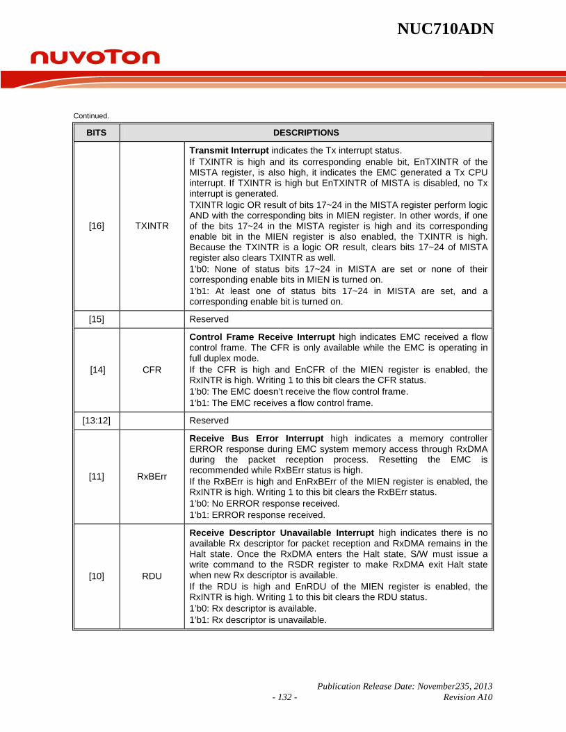
NUC710ADN
Publication Release Date: November235, 2013 - 132 - Revision A10
Continued.
BITS DESCRIPTIONS
[16] TXINTR
Transmit Interrupt indicates the Tx interrupt status. If TXINTR is high and its corresponding enable bit, EnTXINTR of the MISTA register, is also high, it indicates the EMC generated a Tx CPU interrupt. If TXINTR is high but EnTXINTR of MISTA is disabled, no Tx interrupt is generated. TXINTR logic OR result of bits 17~24 in the MISTA register perform logic AND with the corresponding bits in MIEN register. In other words, if one of the bits 17~24 in the MISTA register is high and its corresponding enable bit in the MIEN register is also enabled, the TXINTR is high. Because the TXINTR is a logic OR result, clears bits 17~24 of MISTA register also clears TXINTR as well. 1’b0: None of status bits 17~24 in MISTA are set or none of their corresponding enable bits in MIEN is turned on. 1’b1: At least one of status bits 17~24 in MISTA are set, and a corresponding enable bit is turned on.
[15] Reserved
[14] CFR
Control Frame Receive Interrupt high indicates EMC received a flow control frame. The CFR is only available while the EMC is operating in full duplex mode. If the CFR is high and EnCFR of the MIEN register is enabled, the RxINTR is high. Writing 1 to this bit clears the CFR status. 1’b0: The EMC doesn’t receive the flow control frame. 1’b1: The EMC receives a flow control frame.
[13:12] Reserved
[11] RxBErr
Receive Bus Error Interrupt high indicates a memory controller ERROR response during EMC system memory access through RxDMA during the packet reception process. Resetting the EMC is recommended while RxBErr status is high. If the RxBErr is high and EnRxBErr of the MIEN register is enabled, the RxINTR is high. Writing 1 to this bit clears the RxBErr status. 1’b0: No ERROR response received. 1’b1: ERROR response received.
[10] RDU
Receive Descriptor Unavailable Interrupt high indicates there is no available Rx descriptor for packet reception and RxDMA remains in the Halt state. Once the RxDMA enters the Halt state, S/W must issue a write command to the RSDR register to make RxDMA exit Halt state when new Rx descriptor is available. If the RDU is high and EnRDU of the MIEN register is enabled, the RxINTR is high. Writing 1 to this bit clears the RDU status. 1’b0: Rx descriptor is available. 1’b1: Rx descriptor is unavailable.

NUC710ADN
Publication Release Date: November23, 2013 - 133 - Revision A10
Continued.
BITS DESCRIPTIONS
[9] DENI
DMA Early Notification Interrupt high indicates the EMC has received the Length/Type field of the incoming packet. If DENI is high and EnDENI of the MIEN register is enabled, the RxINTR is high. Writing 1 to this bit clears the DENI status. 1’b0: No incoming packet Length/Type field received. 1’b1: Incoming packet Length/Type field received.
[8] DFOI
Maximum Frame Length Interrupt high indicates the length of the incoming packet has exceeded the length limitation configured in the DMARFC register and the incoming packet is dropped. If the DFOI is high and EnDFO of the MIEN register is enabled, RxINTR is high. Writing 1 to this bit clears the DFOI status. 1’b0: The length of the incoming packet doesn’t exceed the length limitation configured in DMARFC. 1’b1: The length of the incoming packet has exceeded the length limitation configured in DMARFC.
[7] MMP
More Missed Packet Interrupt high indicates the MPCNT, Missed Packet Count, has overflowed. If the MMP is high and EnMMP of the MIEN register is enabled, the RxINTR is high. Writing 1 to this bit clears the MMP status. 1’b0: MPCNT has not rolled over yet. 1’b1: MPCNT has rolled over.
[6] RP
Runt Packet (RP) Interrupt RP high indicates the length of the incoming packet was less than 64 bytes and was dropped. If the ARP of MCMDR register is set, the short packet is regarded as a good packet and the RP is not set. If the RP is high and EnRP of the MIEN register is enabled, RxINTR is high. Writing 1 to this bit clears the RP status. 1’b0: The incoming frame is not a short frame or S/W needs to receive a short frame. 1’b1: The incoming frame is a short frame and was dropped.
[5] ALIE
Alignment Error Interrupt high indicates the length of the incoming frame is not a multiple of byte. If the ALIE is high and EnALIE of the MIEN register is enabled, the RxINTR is high. Writing 1 to this bit clears the ALIE status. 1’b0: The frame length is a multiple of byte. 1’b1: The frame length is not a multiple of byte.

NUC710ADN
Publication Release Date: November235, 2013 - 134 - Revision A10
Continued.
BITS DESCRIPTIONS
[4] RXGD
Receive Good Interrupt high indicates frame reception is complete. If the RXGD is high and EnRXGD of the MIEN register is enabled, the RxINTR is high. Writing 1 to this bit clears the RXGD status. 1’b0: Frame reception is not yet complete. 1’b1: Frame reception is complete.
[3] PTLE
Packet Too Long Interrupt high indicates the length of the incoming packet is greater than 1518 bytes and was dropped. If the ALP of MCMDR register is set, the long packet is regarded as a good packet and PTLE is not set. If the PTLE is high and EnPTLE of the MIEN register is enabled, the RxINTR is high. Writing 1 to this bit clears the PTLE status. 1’b0: Incoming frame is not a long frame or S/W needs to receive a long frame. 1’b1: Incoming frame is a long frame and was dropped.
[2] RXOV
Receive FIFO Overflow Interrupt high indicates RxFIFO overflow occurred during packet reception. While the RxFIFO overflow occurred, the EMC dropped the current receiving packet. If the RxFIFO overflow occurs often, it is recommended to modify the RxFIFO threshold and the RxTHD of the FFTCR register to a higher level. If the RXOV is high and EnRXOV of the MIEN register is enabled, the RxINTR is high. Writing 1 to this bit clears the RXOV status. 1’b0: No RxFIFO overflow occurred during packet reception. 1’b0: RxFIFO overflow occurred during packet reception.
[1] CRCE
CRC Error Interrupt high indicates the incoming packet incurred the CRC error and the packet is dropped. If the AEP of the MCMDR register is set, the CRC error packet is regarded as a good packet and CRCE is not set. If the CRCE is high and EnCRCE of the MIEN register is enabled, the RxINTR is high. Writing 1 to this bit clears the CRCE status. 1’b0: Frame didn’t incur any CRC error. 1’b1: Frame incurred CRC error.
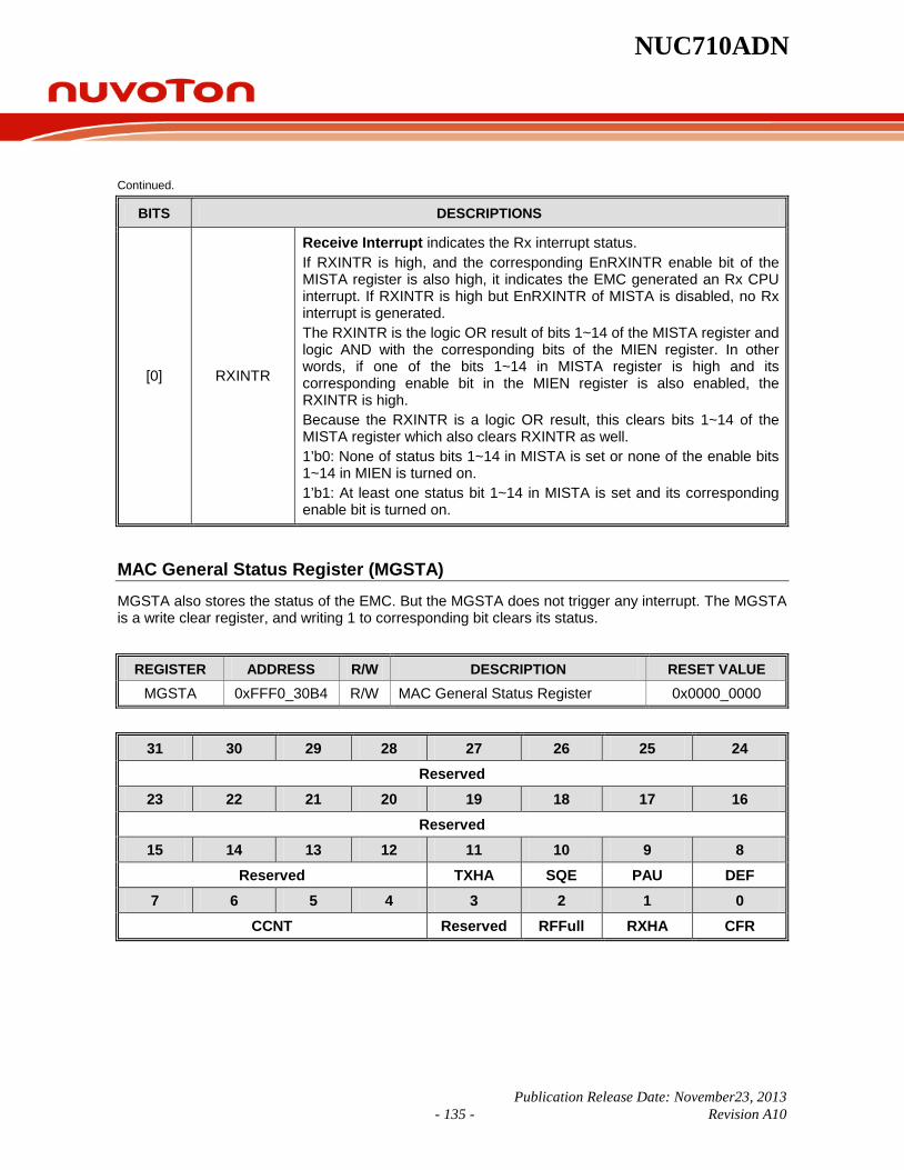
NUC710ADN
Publication Release Date: November23, 2013 - 135 - Revision A10
Continued.
BITS DESCRIPTIONS
[0] RXINTR
Receive Interrupt indicates the Rx interrupt status. If RXINTR is high, and the corresponding EnRXINTR enable bit of the MISTA register is also high, it indicates the EMC generated an Rx CPU interrupt. If RXINTR is high but EnRXINTR of MISTA is disabled, no Rx interrupt is generated. The RXINTR is the logic OR result of bits 1~14 of the MISTA register and logic AND with the corresponding bits of the MIEN register. In other words, if one of the bits 1~14 in MISTA register is high and its corresponding enable bit in the MIEN register is also enabled, the RXINTR is high. Because the RXINTR is a logic OR result, this clears bits 1~14 of the MISTA register which also clears RXINTR as well. 1’b0: None of status bits 1~14 in MISTA is set or none of the enable bits 1~14 in MIEN is turned on. 1’b1: At least one status bit 1~14 in MISTA is set and its corresponding enable bit is turned on.
MAC General Status Register (MGSTA) MGSTA also stores the status of the EMC. But the MGSTA does not trigger any interrupt. The MGSTA is a write clear register, and writing 1 to corresponding bit clears its status.
REGISTER ADDRESS R/W DESCRIPTION RESET VALUE MGSTA 0xFFF0_30B4 R/W MAC General Status Register 0x0000_0000
31 30 29 28 27 26 25 24 Reserved
23 22 21 20 19 18 17 16 Reserved
15 14 13 12 11 10 9 8 Reserved TXHA SQE PAU DEF
7 6 5 4 3 2 1 0 CCNT Reserved RFFull RXHA CFR
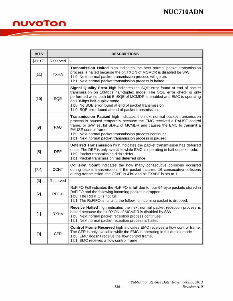
NUC710ADN
Publication Release Date: November235, 2013 - 136 - Revision A10
BITS DESCRIPTIONS
[31:12] Reserved -
[11] TXHA
Transmission Halted high indicates the next normal packet transmission process is halted because the bit TXON of MCMDR is disabled be S/W. 1’b0: Next normal packet transmission process will go on. 1’b1: Next normal packet transmission process is halted.
[10] SQE
Signal Quality Error high indicates the SQE error found at end of packet transmission on 10Mbps half-duplex mode. The SQE error check is only performed while both bit EnSQE of MCMDR is enabled and EMC is operating on 10Mbps half-duplex mode. 1’b0: No SQE error found at end of packet transmission. 1’b0: SQE error found at end of packet transmission.
[9] PAU
Transmission Paused high indicates the next normal packet transmission process is paused temporally because the EMC received a PAUSE control frame, or S/W set bit SDPZ of MCMDR and causes the EMC to transmit a PAUSE control frame. 1’b0: Next normal packet transmission process continues. 1’b1: Next normal packet transmission process is paused.
[8] DEF
Deferred Transmission high indicates the packet transmission has deferred once. The DEF is only available while EMC is operating in half duplex mode. 1’b0: Packet transmission didn’t defer. 1’b1: Packet transmission has deferred once.
[7:4] CCNT Collision Count indicates the how many consecutive collisions occurred during packet transmission. If the packet incurred 16 consecutive collisions during transmission, the CCNT is 4’h0 and bit TXABT is set to 1.
[3] Reserved -
[2] RFFull
RxFIFO Full indicates the RxFIFO is full due to four 64-byte packets stored in RxFIFO and the following incoming packet is dropped. 1’b0: The RxFIFO is not full. 1’b1: The RxFIFO is full and the following incoming packet is dropped.
[1] RXHA
Receive Halted high indicates the next normal packet reception process is halted because the bit RXON of MCMDR is disabled by S/W. 1’b0: Next normal packet reception process continues. 1’b1: Next normal packet reception process is halted.
[0] CFR
Control Frame Received high indicates EMC receives a flow control frame. The CFR is only available while the EMC is operating in full duplex mode. 1’b0: EMC doesn’t receive the flow control frame. 1’b1: EMC receives a flow control frame.

NUC710ADN
Publication Release Date: November23, 2013 - 137 - Revision A10
Missed Packet Count Register (MPCNT) MPCNT stores the number of packets that were dropped due to various types of receive errors. The MPCNT is a read clear register. In addition, S/W also can write an initial value to MPCNT and the missed packet counter starts counting from that initial value. If the missed packet counter overflows, the MMP of MISTA is set.
REGISTER ADDRESS R/W DESCRIPTION RESET VALUE MPCNT 0xFFF0_30B8 R/W Missed Packet Count Register 0x0000_7FFF
31 30 29 28 27 26 25 24 Reserved
23 22 21 20 19 18 17 16 Reserved
15 14 13 12 11 10 9 8 MPC
7 6 5 4 3 2 1 0 MPC
BITS DESCRIPTIONS
[31:16] Reserved -
[15:0] MPC
Miss Packet Count indicates the number of packets that were dropped due to various types of receive errors. The following type of receive error increments the missed packet counter: Incoming packet incurred RxFIFO overflow. Incoming packet is dropped due to disabled RXON. Incoming packet incurred CRC error.
MAC Receive Pause Count Register (MRPC) EMC of NUC710 supports the PAUSE control frame reception and recognition. If the EMC received a PAUSE control frame, the operand field of the PAUSE control frame is extracted and stored in the MRPC register. The MRPC register stores the same while Tx of the EMC receives the PAUSE control frame and halts. The MRPC is read only and writing to this register has no effect.
REGISTER ADDRESS R/W DESCRIPTION RESET VALUE MRPC 0xFFF0_30BC R MAC Receive Pause Count Register 0x0000_0000

NUC710ADN
Publication Release Date: November235, 2013 - 138 - Revision A10
31 30 29 28 27 26 25 24 Reserved
23 22 21 20 19 18 17 16 Reserved
15 14 13 12 11 10 9 8 MRPC
7 6 5 4 3 2 1 0 MRPC
BITS DESCRIPTIONS
[31:16] Reserved -
[15:0] MRPC MAC Receive Pause Count stores the operand field of the PAUSE control frame. It indicates for how many slot times (512 bit times) the Tx of EMC was paused.
MAC Receive Pause Current Count Register (MRPCC) The EMC of NUC710 supports the PAUSE control frame reception and recognition. If EMC received a PAUSE control frame, the operand field of the PAUSE control frame is extracted and stored into a count down timer. The MRPCC shows the current value of that countdown timer for S/W to know how long the EMC Tx was paused. MRPCC is read only and writing to this register has no effect.
REGISTER ADDRESS R/W DESCRIPTION RESET VALUE
MRPCC 0xFFF0_30C0 R MAC Receive Pause Current Count Register 0x0000_0000
31 30 29 28 27 26 25 24
Reserved 23 22 21 20 19 18 17 16
Reserved 15 14 13 12 11 10 9 8
MRPCC 7 6 5 4 3 2 1 0
MRPCC
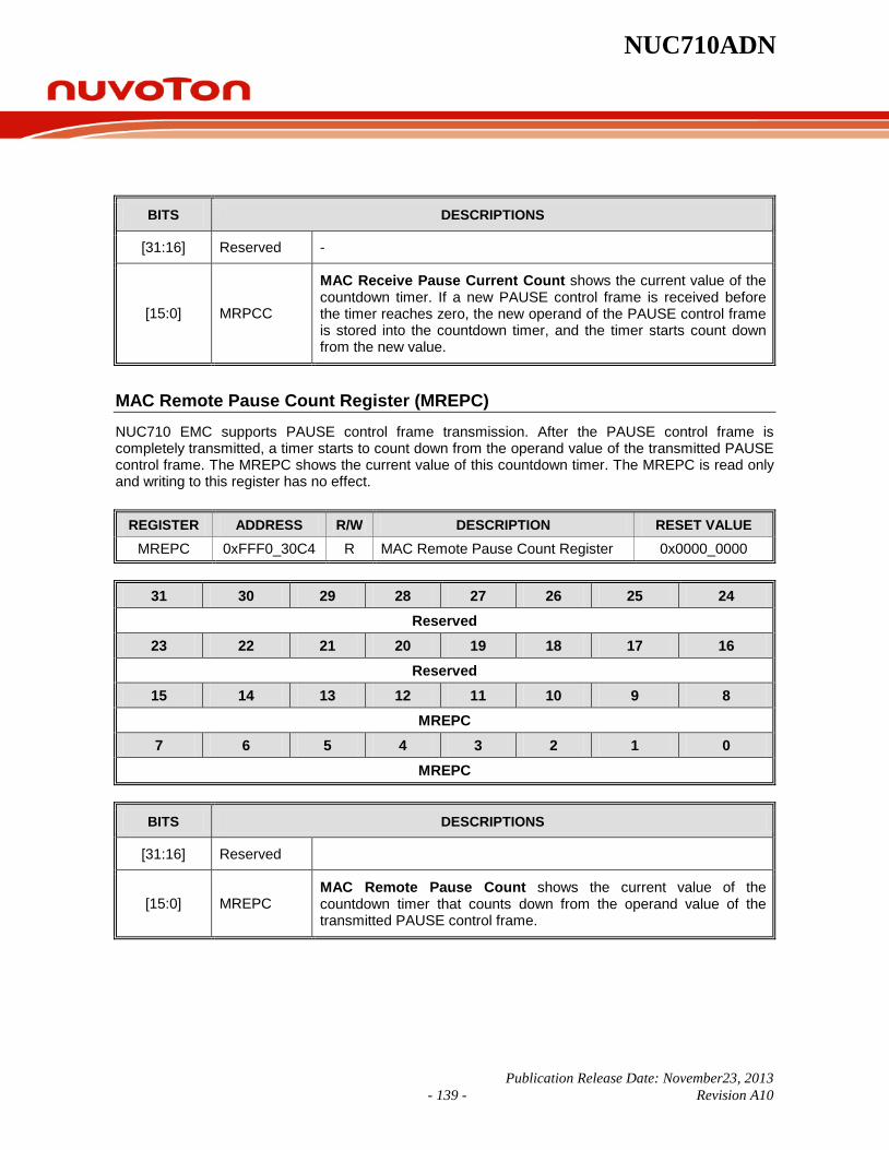
NUC710ADN
Publication Release Date: November23, 2013 - 139 - Revision A10
BITS DESCRIPTIONS
[31:16] Reserved -
[15:0] MRPCC
MAC Receive Pause Current Count shows the current value of the countdown timer. If a new PAUSE control frame is received before the timer reaches zero, the new operand of the PAUSE control frame is stored into the countdown timer, and the timer starts count down from the new value.
MAC Remote Pause Count Register (MREPC) NUC710 EMC supports PAUSE control frame transmission. After the PAUSE control frame is completely transmitted, a timer starts to count down from the operand value of the transmitted PAUSE control frame. The MREPC shows the current value of this countdown timer. The MREPC is read only and writing to this register has no effect.
REGISTER ADDRESS R/W DESCRIPTION RESET VALUE MREPC 0xFFF0_30C4 R MAC Remote Pause Count Register 0x0000_0000
31 30 29 28 27 26 25 24
Reserved 23 22 21 20 19 18 17 16
Reserved 15 14 13 12 11 10 9 8
MREPC 7 6 5 4 3 2 1 0
MREPC
BITS DESCRIPTIONS
[31:16] Reserved
[15:0] MREPC MAC Remote Pause Count shows the current value of the countdown timer that counts down from the operand value of the transmitted PAUSE control frame.

NUC710ADN
Publication Release Date: November235, 2013 - 140 - Revision A10
DMA Receive Frame Status Register (DMARFS) DMARFS is used to store the Length/Type field of each incoming Ethernet packet. This is a “write clear” register and writing to the corresponding bit clears its value.
REGISTER ADDRESS R/W DESCRIPTION RESET VALUE DMARFS 0xFFF0_30C8 R/W DMA Receive Frame Status Register 0x0000_0000
31 30 29 28 27 26 25 24 Reserved
23 22 21 20 19 18 17 16 Reserved
15 14 13 12 11 10 9 8 RXFLT
7 6 5 4 3 2 1 0 RXFLT
BITS DESCRIPTIONS
[31:16] Reserved
[15:0] RXFLT
Receive Frame Length/Type stores the Length/Type field of each incoming Ethernet packet. If the bit EnDEN of MIEN is enabled and the Length/Type field of the incoming packet were received, the DENI bit of MISTA is set and triggers an interrupt. And, the contents of Length/Type field are stored in RXFLT.
Current Transmit Descriptor Start Address Register (CTXDSA) CTXDSA stores the start address of the Tx descriptor that is currently used by the TxDMA. CTXDSA is read only and writing to this register has no effect.
REGISTER ADDRESS R/W DESCRIPTION RESET VALUE
CTXDSA 0xFFF0_30CC R Current Transmit Descriptor Start Address Register 0x0000_0000
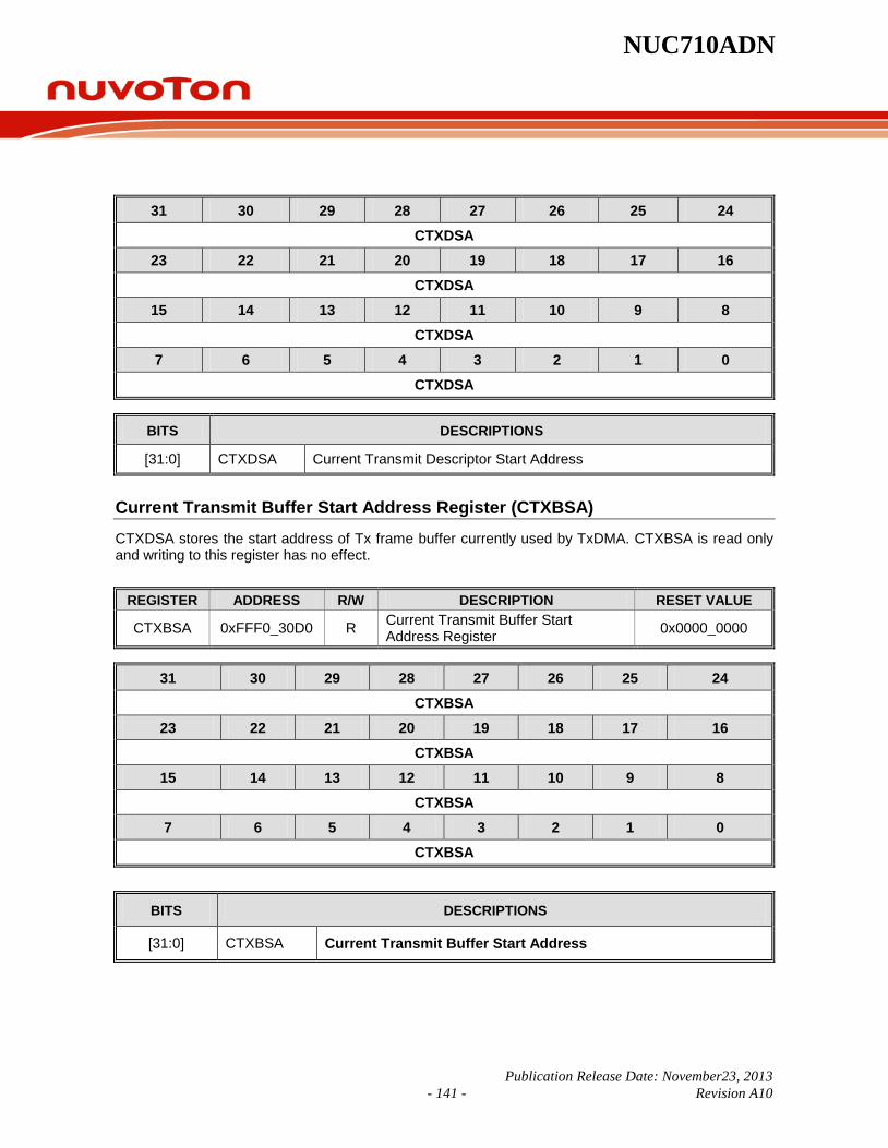
NUC710ADN
Publication Release Date: November23, 2013 - 141 - Revision A10
31 30 29 28 27 26 25 24 CTXDSA
23 22 21 20 19 18 17 16 CTXDSA
15 14 13 12 11 10 9 8 CTXDSA
7 6 5 4 3 2 1 0 CTXDSA
BITS DESCRIPTIONS
[31:0] CTXDSA Current Transmit Descriptor Start Address
Current Transmit Buffer Start Address Register (CTXBSA) CTXDSA stores the start address of Tx frame buffer currently used by TxDMA. CTXBSA is read only and writing to this register has no effect.
REGISTER ADDRESS R/W DESCRIPTION RESET VALUE
CTXBSA 0xFFF0_30D0 R Current Transmit Buffer Start Address Register 0x0000_0000
31 30 29 28 27 26 25 24 CTXBSA
23 22 21 20 19 18 17 16 CTXBSA
15 14 13 12 11 10 9 8 CTXBSA
7 6 5 4 3 2 1 0 CTXBSA
BITS DESCRIPTIONS
[31:0] CTXBSA Current Transmit Buffer Start Address

NUC710ADN
Publication Release Date: November235, 2013 - 142 - Revision A10
Current Receive Descriptor Start Address Register (CRXDSA) CRXDSA stores the start address of the Rx descriptor currently used by RxDMA. CRXDSA is read only and writing to this register has no effect.
REGISTER ADDRESS R/W DESCRIPTION RESET VALUE
CRXDSA 0xFFF0_30D4 R Current Receive Descriptor Start Address Register 0x0000_0000
31 30 29 28 27 26 25 24 CRXDSA
23 22 21 20 19 18 17 16 CRXDSA
15 14 13 12 11 10 9 8 CRXDSA
7 6 5 4 3 2 1 0 CRXDSA
BITS DESCRIPTIONS
[31:0] CRXDSA Current Receive Descriptor Start Address
Current Receive Buffer Start Address Register (CRXBSA) The CRXBSA stores the start address of Rx frame buffer currently used by RxDMA. The CRXBSA is read only and writing to this register has no effect.
REGISTER ADDRESS R/W DESCRIPTION RESET VALUE
CRXBSA 0xFFF0_30D8 R Current Receive Buffer Start Address Register 0x0000_0000
31 30 29 28 27 26 25 24 CRXBSA
23 22 21 20 19 18 17 16 CRXBSA
15 14 13 12 11 10 9 8 CRXBSA
7 6 5 4 3 2 1 0 CRXBSA
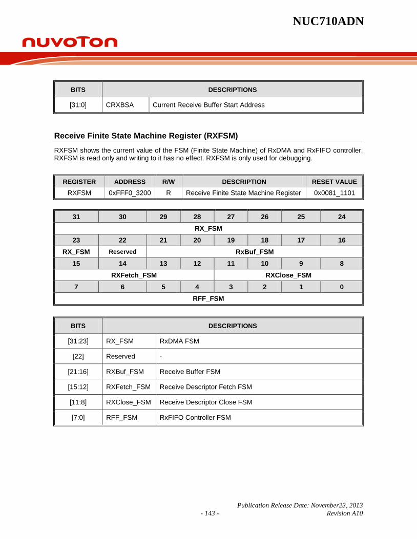
NUC710ADN
Publication Release Date: November23, 2013 - 143 - Revision A10
BITS DESCRIPTIONS
[31:0] CRXBSA Current Receive Buffer Start Address
Receive Finite State Machine Register (RXFSM) RXFSM shows the current value of the FSM (Finite State Machine) of RxDMA and RxFIFO controller. RXFSM is read only and writing to it has no effect. RXFSM is only used for debugging.
REGISTER ADDRESS R/W DESCRIPTION RESET VALUE RXFSM 0xFFF0_3200 R Receive Finite State Machine Register 0x0081_1101
31 30 29 28 27 26 25 24 RX_FSM
23 22 21 20 19 18 17 16 RX_FSM Reserved RxBuf_FSM
15 14 13 12 11 10 9 8 RXFetch_FSM RXClose_FSM
7 6 5 4 3 2 1 0 RFF_FSM
BITS DESCRIPTIONS
[31:23] RX_FSM RxDMA FSM
[22] Reserved -
[21:16] RXBuf_FSM Receive Buffer FSM
[15:12] RXFetch_FSM Receive Descriptor Fetch FSM
[11:8] RXClose_FSM Receive Descriptor Close FSM
[7:0] RFF_FSM RxFIFO Controller FSM

NUC710ADN
Publication Release Date: November235, 2013 - 144 - Revision A10
Transmit Finite State Machine Register (TXFSM) TXFSM shows the current value of the FSM (Finite State Machine) of TxDMA and TxFIFO controller. The TXFSM is read only and writing to it has no effect. The TXFSM is only used for debugging.
REGISTER ADDRESS R/W DESCRIPTION RESET VALUE TXFSM 0xFFF0_3204 R Transmit Finite State Machine Register 0x0101_1101
31 30 29 28 27 26 25 24 TX_FSM
23 22 21 20 19 18 17 16 Reserved TxBuf_FSM
15 14 13 12 11 10 9 8 TXFetch_FSM TXClose_FSM
7 6 5 4 3 2 1 0 Reserved TFF_FSM
BITS DESCRIPTIONS
[31:24] TX_FSM TxDMA FSM
[23:22] Reserved -
[21:16] TXBuf_FSM Transmit Buffer FSM
[15:12] TXFetch_FSM Transmit Descriptor Fetch FSM
[11:8] TXClose_FSM Transmit Descriptor Close FSM
[7:5] Reserved -
[4:0] TFF_FSM TxFIFO Controller FSM
Finite State Machine Register 0 (FSM0) FSM0 shows the current value of the FSM (Finite State Machine) in the EMC function module. FSM0 is read only and writing to it has no effect. The FSM0 is only used for debugging.
REGISTER ADDRESS R/W DESCRIPTION RESET VALUE FSM0 0xFFF0_3208 R Finite State Machine Register 0 0x0001_0101

NUC710ADN
Publication Release Date: November23, 2013 - 145 - Revision A10
31 30 29 28 27 26 25 24 Reserved TXMAC_FSM
23 22 21 20 19 18 17 16 TXMAC_FSM
15 14 13 12 11 10 9 8 Reserved TXDefer_FSM
7 6 5 4 3 2 1 0 STA_FSM
BITS DESCRIPTIONS
[31:26] Reserved -
[25:16] TXMAC_FSM TxMAC FSM
[15:14] Reserved -
[13:8] TXDefer_FSM Transmit Defer Process FSM
[7:0] STA_FSM MII Management I/F FSM
Finite State Machine Register 1 (FSM1) FSM1 shows the current value of the FSM (Finite State Machine) in the EMC function module. FSM1 is read only and writing to it has no effect. The FSM1 is only used for debugging.
Register Address R/W Description Reset Value FSM1 0xFFF0_320C R Finite State Machine Register 1 0x1100_0100
31 30 29 28 27 26 25 24 Reserved ARB_FSM TxPause_FSM
23 22 21 20 19 18 17 16 Reserved
15 14 13 12 11 10 9 8 Reserved AHB_FSM
7 6 5 4 3 2 1 0 Reserved
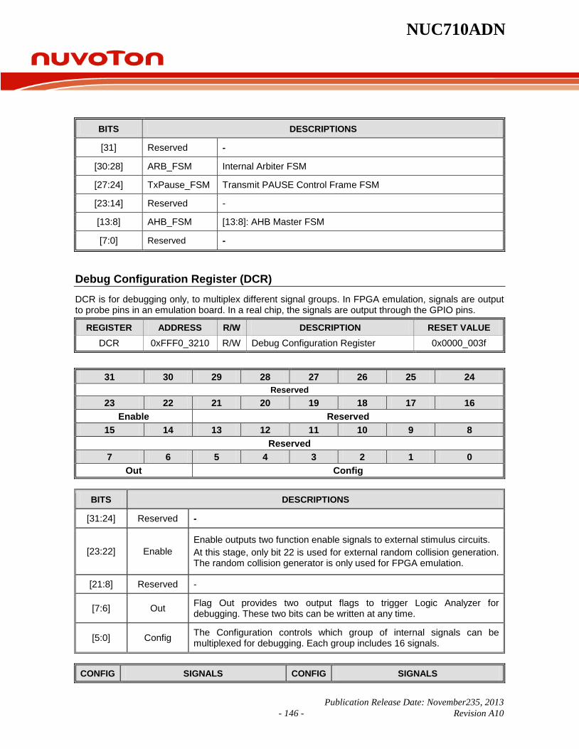
NUC710ADN
Publication Release Date: November235, 2013 - 146 - Revision A10
BITS DESCRIPTIONS
[31] Reserved -
[30:28] ARB_FSM Internal Arbiter FSM
[27:24] TxPause_FSM Transmit PAUSE Control Frame FSM
[23:14] Reserved -
[13:8] AHB_FSM [13:8]: AHB Master FSM
[7:0] Reserved -
Debug Configuration Register (DCR) DCR is for debugging only, to multiplex different signal groups. In FPGA emulation, signals are output to probe pins in an emulation board. In a real chip, the signals are output through the GPIO pins.
REGISTER ADDRESS R/W DESCRIPTION RESET VALUE DCR 0xFFF0_3210 R/W Debug Configuration Register 0x0000_003f
31 30 29 28 27 26 25 24 Reserved
23 22 21 20 19 18 17 16 Enable Reserved
15 14 13 12 11 10 9 8 Reserved
7 6 5 4 3 2 1 0 Out Config
BITS DESCRIPTIONS
[31:24] Reserved -
[23:22] Enable Enable outputs two function enable signals to external stimulus circuits. At this stage, only bit 22 is used for external random collision generation. The random collision generator is only used for FPGA emulation.
[21:8] Reserved -
[7:6] Out Flag Out provides two output flags to trigger Logic Analyzer for debugging. These two bits can be written at any time.
[5:0] Config The Configuration controls which group of internal signals can be multiplexed for debugging. Each group includes 16 signals.
CONFIG SIGNALS CONFIG SIGNALS

NUC710ADN
Publication Release Date: November23, 2013 - 147 - Revision A10
6’h00
OUT [6], TransDone, GrantLost, Trans_CTR [4:0], LAST, TransCtrExpire, DMode_AHB_CS [5:0]
6’h01 OUT [6], DMode_TxBuf_CS [6:0] DMode_TXFSM_CS [7:0]
6’h02 OUT [6], DMode_RXBuf_CS [5:0], DMode_RXFSM_CS [8:0]
6’h03 OUT [6], TXFIFO_HT, TXFIFO_LT, DMode_TFF_CS [4:0], DMode_RFF_CS [7:0]
6’h04 TxBuf_DRDY, TFF_WPTR [5:0], TX_START, TXSTART, READ, TFF_RPTR [5:0]
6’h05
WRITE, RFF_WPTR [5:0], RXFIFO_HT, RXFIFO_LT, RxBuf_ACK, RFF_RPTR [5:0]
6’h06 R0_PTLE, RxStart, SFD, WasSFD, RxFrame, WrByte, Rx_OvFlow, 1’b0, R0_RBC [7:0]
6’h07
R0_CRCE, RX_DV_In, SynStart, R0_DB, Rx_OvFlow, WRITECTR [2:0], RxByte [7:0]
6’h08 Reserved 6’h09 Reserved
6’h0A
OUT [7:6], RegMISTA_Rx_W, RXERR_sync, R0_CRCE, R0_PTLE, R0_RP, RegMISTA_Tx_W, T0_EXDEF, T0_TXABT, T0_CCNT [3:0], 2’b00
6’h0B
OUT [7:6], MCMDR_SDPZ_Clr, RegMCMDR_SDPZ_Clr, DMode_Pause_CS [3:0], MacCtlFra, PauseFra, PauseTx, MacCtlFra_sync, PauseFra_sync, PAUSE, Pause_en, FDUP
6’h0C
OUT [7:6], FrameWPtr [1:0], FrameRPtr [1:0], RFF_One, FrameWPtr_Inc, FrameRPtr_Inc, Rounding, NexPktStartPtr [5:0]
6’h0D
OUT [7:6], ARB_REQ_Set, ARB_REQ_Clr, DMode_ARB_CS [2:0], TransDone, GrantLost, TransCtrExpire, Trans_CTR [4:0], BURST
6’h0E
R0_CRCE, Rx_OvFlow, R0_MRE, CRCERR, DAMATCH, RxFrame, SFD, RxMIIErr, SynStart, Hi_Lo_Syn, New_DataValid, L_RxFrame, RxStart, DataValid, Hi_Lo, RX_DV_In
6’h0F OUT [6], WRITE, RFF_WPTR [5:0], RxReuse, RxBuf_ACK, RFF_RPTR [5:0]
6’h10 WRITE, RFF_CS [7:1], RFF_WPTR [5:0], RXERR_sync, RxReuse
6’h11
OUT [6], TX_CLK, TX_EN, TXD [3:0], RX_CLK, RX_DV, RX_ER, RXD [3:0], CRS, COL
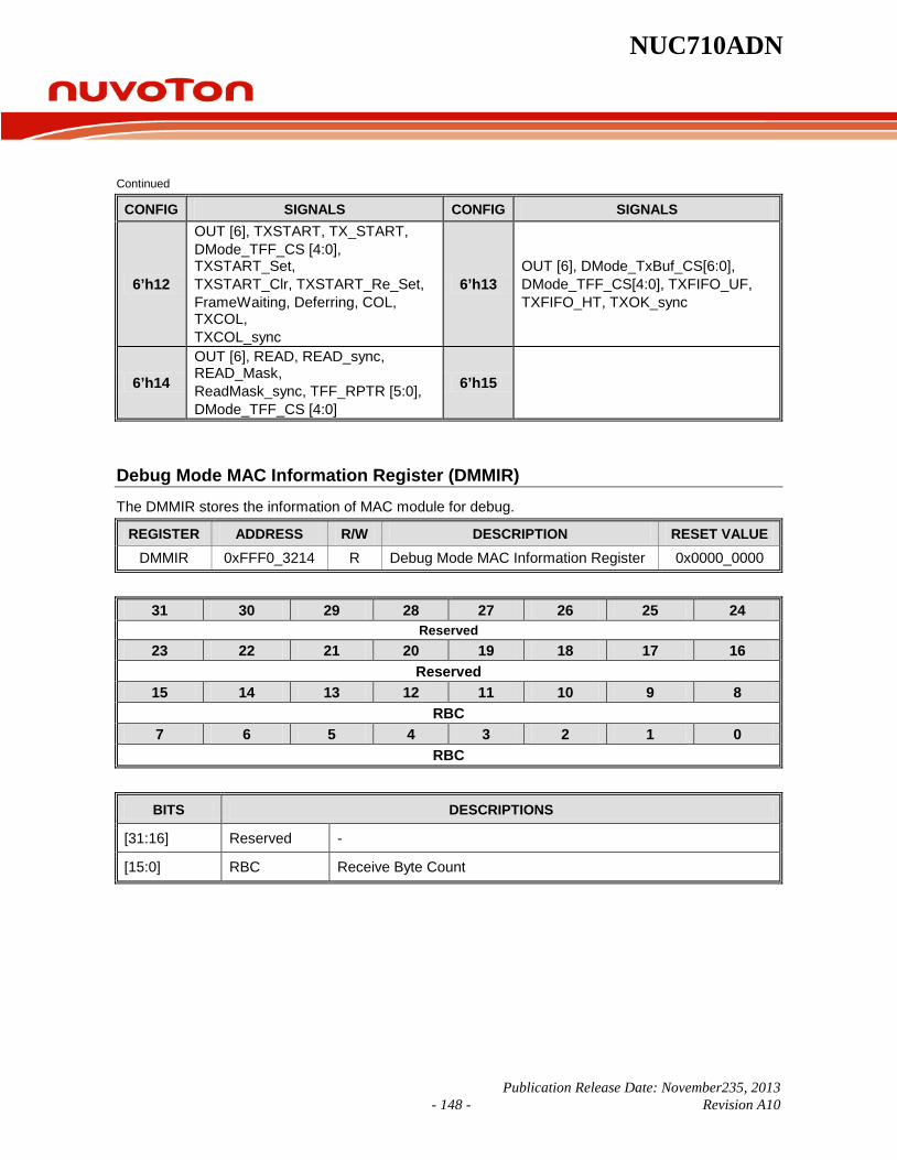
NUC710ADN
Publication Release Date: November235, 2013 - 148 - Revision A10
Continued
CONFIG SIGNALS CONFIG SIGNALS
6’h12
OUT [6], TXSTART, TX_START, DMode_TFF_CS [4:0], TXSTART_Set, TXSTART_Clr, TXSTART_Re_Set, FrameWaiting, Deferring, COL, TXCOL, TXCOL_sync
6’h13 OUT [6], DMode_TxBuf_CS[6:0], DMode_TFF_CS[4:0], TXFIFO_UF, TXFIFO_HT, TXOK_sync
6’h14
OUT [6], READ, READ_sync, READ_Mask, ReadMask_sync, TFF_RPTR [5:0], DMode_TFF_CS [4:0]
6’h15
Debug Mode MAC Information Register (DMMIR) The DMMIR stores the information of MAC module for debug.
REGISTER ADDRESS R/W DESCRIPTION RESET VALUE DMMIR 0xFFF0_3214 R Debug Mode MAC Information Register 0x0000_0000
31 30 29 28 27 26 25 24 Reserved
23 22 21 20 19 18 17 16 Reserved
15 14 13 12 11 10 9 8 RBC
7 6 5 4 3 2 1 0 RBC
BITS DESCRIPTIONS
[31:16] Reserved -
[15:0] RBC Receive Byte Count

NUC710ADN
Publication Release Date: November23, 2013 - 149 - Revision A10
BIST Mode Register (BISTR) BISTR controls the BIST (Built In Self Test) for embedded SRAM, 256B for RxFIFO and 256B for TxFIFO.
REGISTER ADDRESS R/W DESCRIPTION RESET VALUE BISTR 0xFFF0_3300 R/W BIST Mode Register 0x0000_0000
31 30 29 28 27 26 25 24 Reserved
23 22 21 20 19 18 17 16 Reserved
15 14 13 12 11 10 9 8 Reserved
7 6 5 4 3 2 1 0 Reserved BistFail Finish BMEn
BITS DESCRIPTIONS
[31:5] Reserved -
[3:2] BistFail
BISTFail indicates if the BIST test failed or succeeded. If BistFail is low at the end the embedded SRAM passed the BIST test, otherwise it failed. BistFail goes high when the BIST detects the error and remains high during BIST operation. If BistFail[2] high indicates the embedded SRAM for TxFIFO BIST test failed. If BistFail[3] high indicates the embedded SRAM for RxFIFO BIST test failed. The BistFail is a “write clear field”, and writing 1 to this field clears its contents; writing 0 has no effect.
[1] Finish
BIST Operation Finish indicates the end of the BIST operation. When the BIST controller finishes all operations, this bit is high. The Finish is a “write clear” field, and writing 1 to this field clears the contents; writing 0 has no effect.
[0] BMEn
BIST Mode Enable is used to enable BIST operation. If high, it enables the BIST controller to perform an embedded SRAM test. This bit is also used to reset the BIST circuit. It is necessary to reset the BIST circuit for at least one clock cycle in order to initialize the BIST properly. The BMEn can be disabled by writing 0.

NUC710ADN
Publication Release Date: November235, 2013 - 150 - Revision A10
6.6 GDMA Controller NUC710 has a two-channel general DMA controller, called the GDMA. The two-channel GDMA performs the following data transfers without the CPU intervention: Memory-to-memory (memory to/from memory) Memory –to – IO IO- to -memory
The on-chip GDMA can be started by the software or external DMA request nXDREQ. Software can also be used to restart the GDMA operation after it has been stopped. The CPU can recognize the completion of a GDMA operation by software polling or when it receives an internal GDMA interrupt. The NUC710 GDMA controller can increment source or destination address, decrement them as well, and conduct 8-bit (byte), 16-bit (half-word), or 32-bit (word) data transfers.
The GDMA includes the following features AMBA AHB compliant Supports 4-data burst mode to boost performance Provides support for external GDMA device Demand mode speeds up external GDMA operations
6.6.1 GDMA Functional Description The GDMA directly transfers data between source and destination. The GDMA starts to transfer data after it receives service requests from nXDREQ signal or software. When the entire data has completely transferred, the GDMA becomes idle. Nevertheless, if another transfer is needed, then the GDMA must be programmed again. There are three transfer modes:
Single Mode Single mode requires a GDMA request for each data transfer. A GDMA request (nXDREQ or software) causes one byte, one half-word, or one word to transfer if the 4-data burst mode is disabled, or four times of transfer width is the 4-data burst mode is enabled.
Block Mode
The assertion of a single GDMA request causes all of the data to be transferred in a single operation. The GDMA transfer is completed when the current transfer count register reaches zero.
Demand Mode
The GDMA continues transferring data until the GDMA request input nXDREQ becomes inactive.

NUC710ADN
Publication Release Date: November23, 2013 - 151 - Revision A10
6.6.2 GDMA Register Map R: read only, W: write only, R/W: both read and write, C: Only value 0 can be written
REGISTER ADDRESS R/W DESCRIPTION RESET VALUE
Channel 0 GDMA_CTL0 0xFFF0_4000 R/W Channel 0 Control Register 0x0000_0000
GDMA_SRCB0 0xFFF0_4004 R/W Channel 0 Source Base Address Register 0x0000_0000
GDMA_DSTB0 0xFFF0_4008 R/W Channel 0 Destination Base Address Register 0x0000_0000
GDMA_TCNT0 0xFFF0_400C R/W Channel 0 Transfer Count Register 0x0000_0000
GDMA_CSRC0 0xFFF0_4010 R Channel 0 Current Source Address Register 0x0000_0000
GDMA_CDST0 0xFFF0_4014 R Channel 0 Current Destination Address Register 0x0000_0000
GDMA_CTCNT0 0xFFF0_4018 R Channel 0 Current Transfer Count Register 0x0000_0000
Channel 1 GDMA_CTL1 0xFFF0_4020 R/W Channel 1 Control Register 0x0000_0000
GDMA_SRCB1 0xFFF0_4024 R/W Channel 1 Source Base Address Register 0x0000_0000
GDMA_DSTB1 0xFFF0_4028 R/W Channel 1 Destination Base Address Register 0x0000_0000
GDMA_TCNT1 0xFFF0_402C R/W Channel 1 Transfer Count Register 0x0000_0000
GDMA_CSRC1 0xFFF0_4030 R Channel 1 Current Source Address Register 0x0000_0000
GDMA_CDST1 0xFFF0_4034 R Channel 1 Current Destination Address Register 0x0000_0000
GDMA_CTCNT1 0xFFF0_4038 R Channel 1 Current Transfer Count Register 0x0000_0000
Channel 0/1 Control Register (GDMA_CTL0, GDMA_CTL1)
REGISTER ADDRESS R/W DESCRIPTION RESET VALUE GDMA_CTL0 0xFFF0_4000 R/W Channel 0 Control Register 0x0000_0000 GDMA_CTL1 0xFFF0_4020 R/W Channel 1 Control Register 0x0000_0000
31 30 29 28 27 26 25 24 RESERVED TC_WIDTH REQ_SEL REQ_ATV ACK_ATV
23 22 21 20 19 18 17 16 RW_TC SABNDERR DABNDERR GDMAERR AUTOIEN TC BLOCK SOFTREQ
15 14 13 12 11 10 9 8 DM RESERVED TWS SBMS RESERVED BME SIEN
7 6 5 4 3 2 1 0 SAFIX DAFIX SADIR DADIR GDMAMS RESERVED GDMAEN

NUC710ADN
Publication Release Date: November235, 2013 - 152 - Revision A10
BITS DESCRIPTIONS
[31] RESERVED -
[30:28] TC_WIDTH nRTC/nWTC active width selection, from 1 to 7 HCLK cycles.
[27:26] REQ_SEL
External request pin selection, if GDMAMS [3:2]=00, REQ_SEL is don’t care. If REQ_SEL [27:26]=00, external request don’t use. If REQ_SEL [27:26]=01, use nXDREQ. If REQ_SEL [27:26]=10, external request don’t use. If REQ_SEL [27:26]=11, external request don’t use.
[25] REQ_ATV nXDREQ High/Low active selection 1’b0 = nXDREQ is LOW active. 1’b1 = nXDREQ is HIGH active.
[24] ACK_ATV nXDACK High/Low active selection 1’b0 = nXDACK is LOW active. 1’b1 = nXDACK is HIGH active.
[23] RW_TC Read/Write terminal count output selection. 1’b0 = output to nRTC. 1’b1 = output to nWTC.
[22] SABNDERR
Source address Boundary alignment Error flag If TWS [13:12]=10, GDMA_SRCB [1:0] should be 00 If TWS [13:12]=01, GDMA_SRCB [0] should be 0 The address boundary alignment should be depended on TWS [13:12]. 1’b0 = the GDMA_SRCB is on the boundary alignment. 1’b1 = the GDMA_SRCB not on the boundary alignment The SABNDERR register bits just can be read only.
[21] DABNDERR
Destination address Boundary alignment Error flag If TWS [13:12]=10, GDMA_DSTB [1:0] should be 00 If TWS [13:12]=01, GDMA_DSTB [0] should be 0 The address boundary alignment should be depended on TWS [13:12]. 1’b0 = the GDMA_DSTB is on the boundary alignment. 1’b1 = the GDMA_DSTB not on the boundary alignment The DABNDERR register bits just can be read only.
[20] GDMATERR
GDMA Transfer Error 1’b0 = No error occurs 1’b1 = Hardware sets this bit on a GDMA transfer failure Transfer error will generate GDMA interrupt

NUC710ADN
Publication Release Date: November23, 2013 - 153 - Revision A10
Continued
BITS DESCRIPTIONS
[19] AUTOIEN
Auto initialization Enable 1’b0 = Disables auto initialization 1’b1 = Enables auto initialization, the GDMA_CSRC0/1, GDMA_CDST0/1,and GDMA_CTCNT0/1 registers are updated by the GDMA_SRC0/1,GDMA_DST0/1,and GDMA_TCNT0/1 registers automatically when transfer is complete.
[18] TC
Terminal Count 1’b0 = Channel does not expire 1’b1 = Channel expires; this bit is set only by GDMA hardware, and clear by software to write logic 0. TC [18] is the GDMA interrupt flag. TC [18] or GDMATERR[20] will generate interrupt
[17] BLOCK Bus Lock 1’b0 = Unlocks the bus during the period of transfer 1’b1 = Locks the bus during the period of transfer
[16] SOFTREQ
Software Triggered GDMA Request Software can request the GDMA transfer service by setting this bit to 1. This bit is automatically cleared by hardware when the transfer is completed. This bit is available only while GDMAMS [3:2] register bits are set on software mode (memory to memory).
[15] DM
Demand Mode 1’b0 = Normal external GDMA mode 1’b1 = When this bit is set to 1, the external GDMA operation is sped up. When external GDMA device is operating in the demand mode, the GDMA transfers data as long as the external GDMA request signal nXDREQ is active. The amount of data transferred depends on how long the nXDREQ is active. When the nXDREQ is active and GDMA gets the bus in Demand mode, DMA holds the system bus until the nXDREQ signal becomes non-active. Therefore, the period of the active nXDREQ signal should be carefully tuned such that the entire operation does not exceed an acceptable interval (for example, during a DRAM refresh operation).
[14] Reserved -
[11] SBMS
Single/Block Mode Select 1’b0 = Selects single mode. It requires an external GDMA request for every GDMA operation. 1’b1 = Selects block mode. It requires a single external GDMA request during the atomic GDMA operation. An atomic GDMA operation is defined as the sequence of GDMA operations until the transfer count register reaches zero.
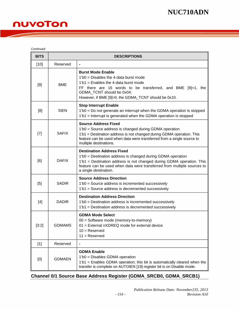
NUC710ADN
Publication Release Date: November235, 2013 - 154 - Revision A10
Continued
BITS DESCRIPTIONS
[10] Reserved -
[9] BME
Burst Mode Enable 1’b0 = Disables the 4-data burst mode 1’b1 = Enables the 4-data burst mode FF there are 16 words to be transferred, and BME [9]=1, the GDMA_TCNT should be 0x04; However, if BME [9]=0, the GDMA_TCNT should be 0x10.
[8] SIEN Stop Interrupt Enable 1’b0 = Do not generate an interrupt when the GDMA operation is stopped 1’b1 = Interrupt is generated when the GDMA operation is stopped
[7] SAFIX
Source Address Fixed 1’b0 = Source address is changed during GDMA operation 1’b1 = Destination address is not changed during GDMA operation. This feature can be used when data were transferred from a single source to multiple destinations.
[6] DAFIX
Destination Address Fixed 1’b0 = Destination address is changed during GDMA operation 1’b1 = Destination address is not changed during GDMA operation. This feature can be used when data were transferred from multiple sources to a single destination.
[5] SADIR Source Address Direction 1’b0 = Source address is incremented successively 1’b1 = Source address is decremented successively
[4] DADIR Destination Address Direction 1’b0 = Destination address is incremented successively 1’b1 = Destination address is decremented successively
[3:2] GDMAMS
GDMA Mode Select 00 = Software mode (memory-to-memory) 01 = External nXDREQ mode for external device 10 = Reserved 11 = Reserved
[1] Reserved -
[0] GDMAEN
GDMA Enable 1’b0 = Disables GDMA operation 1’b1 = Enables GDMA operation; this bit is automatically cleared when the transfer is complete on AUTOIEN [19] register bit is on Disable mode.
Channel 0/1 Source Base Address Register (GDMA_SRCB0, GDMA_SRCB1)

NUC710ADN
Publication Release Date: November23, 2013 - 155 - Revision A10
GDMA channel starts reading its data from the source address as defined in this source base address register.
REGISTER ADDRESS R/W DESCRIPTION RESET VALUE
GDMA_SRCB0 0xFFF0_4004 R/W Channel 0 Source Base Address Register 0x0000_0000
GDMA_SRCB1 0xFFF0_4024 R/W Channel 1 Source Base Address Register 0x0000_0000
31 30 29 28 27 26 25 24 SRC_BASE_ADDR [31:24]
23 22 21 20 19 18 17 16 SRC_BASE_ADDR [23:16]
15 14 13 12 11 10 9 8 SRC_BASE_ADDR [15:8]
7 6 5 4 3 2 1 0 SRC_BASE_ADDR [7:0]
BITS DESCRIPTIONS
[31:0] SRC_BASE_ADDR 32-bit Source Base Address
Channel 0/1 Destination Base Address Register (GDMA_DSTB0, DMA_DSTB1) Channel 0/1 Destination Base Address Register (GDMA_DSTB0, GDMA_DSTB1) GDMA channel starts writing its data to the destination address as defined in this destination base address register. During a block transfer, the GDMA determines successive destination addresses by adding to or subtracting from the destination base address.
REGISTER ADDRESS R/W DESCRIPTION RESET VALUE
GDMA_DSTB0 0xFFF0_4008 R/W Channel 0 Destination Base Address Register 0x0000_0000
GDMA_DSTB1 0xFFF0_4028 R/W Channel 1 Destination Base Address Register 0x0000_0000
31 30 29 28 27 26 25 24 DST_BASE_ADDR [31:24]
23 22 21 20 19 18 17 16 DST_BASE_ADDR [23:16]
15 14 13 12 11 10 9 8 DST_BASE_ADDR [15:8]
7 6 5 4 3 2 1 0 DST_BASE_ADDR [7:0]
BITS DESCRIPTIONS
[31:0] DST_BASE_ADDR 32-bit Destination Base Address

NUC710ADN
Publication Release Date: November235, 2013 - 156 - Revision A10
Channel 0/1 Transfer Count Register (GDMA_TCNT0, GDMA_TCNT1)
REGISTER ADDRESS R/W DESCRIPTION RESET VALUE GDMA_TCNT0 0xFFF0_400C R/W Channel 0 Transfer Count Register 0x0000_0000 GDMA_TCNT1 0xFFF0_402C R/W Channel 1 Transfer Count Register 0x0000_0000
31 30 29 28 27 26 25 24 Reserved
23 22 21 20 19 18 17 16 TFR_CNT [23:16]
15 14 13 12 11 10 9 8 TFR_CNT [15:8]
7 6 5 4 3 2 1 0 TFR_CNT [7:0]
BITS DESCRIPTIONS
[31:24] Reserved -
[23:0] TFR_CNT TFR_CNT represents the required number of GDMA transfers. The maximum transfer count is 16M –1.
Channel 0/1 Current Source Register (GDMA_CSRC0, GDMA_CSRC1)
REGISTER ADDRESS R/W DESCRIPTION RESET VALUE
GDMA_CSRC0 0xFFF0_4010 R Channel 0 Current Source Address Register 0x0000_0000 GDMA_CSRC1 0xFFF0_4030 R Channel 1 Current Source Address Register 0x0000_0000
31 30 29 28 27 26 25 24 CURRENT_SRC_ADDR [31:24]
23 22 21 20 19 18 17 16 CURRENT_SRC_ADDR [23:16]
15 14 13 12 11 10 9 8 CURRENT_SRC_ADDR [15:8]
7 6 5 4 3 2 1 0 CURRENT_SRC_ADDR [7:0]
BITS DESCRIPTIONS

NUC710ADN
Publication Release Date: November23, 2013 - 157 - Revision A10
[31:0] CURRENT_SRC_ADDR
32-bit Current Source Address indicates the source address where the GDMA transfer occurred. During a block transfer, the GDMA determines successive source addresses by adding to or subtracting from the source base address. Depending on the settings you make to the control register, the current source address remains the same or is incremented or decremented.
Channel 0/1 Current Destination Register (GDMA_CDST0, GDMA_CDST1)
REGISTER ADDRESS R/W DESCRIPTION RESET VALUE
GDMA_CDST0 0xFFF0_4014 R Channel 0 Current Destination Address Register 0x0000_0000 GDMA_CDST1 0xFFF0_4034 R Channel 1 Current Destination Address Register 0x0000_0000
31 30 29 28 27 26 25 24 CURRENT_DST_ADDR [31:24]
23 22 21 20 19 18 17 16 CURRENT_DST_ADDR [23:16]
15 14 13 12 11 10 9 8 CURRENT_DST_ADDR [15:8]
7 6 5 4 3 2 1 0 CURRENT_DST_ADDR [7:0]
BITS DESCRIPTIONS
[31:0] CURRENT_DST_ADDR
32-bit Current Destination Address indicates the destination address where the GDMA transfer occurred. During a block transfer, the GDMA determines successive destination addresses by adding to or subtracting from the destination base address. Depending on the settings you make to the control register, the current destination address will remain the same or is incremented or decremented.
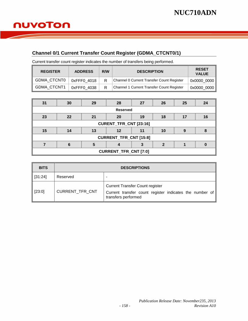
NUC710ADN
Publication Release Date: November235, 2013 - 158 - Revision A10
Channel 0/1 Current Transfer Count Register (GDMA_CTCNT0/1) Current transfer count register indicates the number of transfers being performed.
REGISTER ADDRESS R/W DESCRIPTION RESET VALUE
GDMA_CTCNT0 0xFFF0_4018 R Channel 0 Current Transfer Count Register 0x0000_0000 GDMA_CTCNT1 0xFFF0_4038 R Channel 1 Current Transfer Count Register 0x0000_0000
31 30 29 28 27 26 25 24 Reserved
23 22 21 20 19 18 17 16 CURENT_TFR_CNT [23:16]
15 14 13 12 11 10 9 8 CURRENT_TFR_CNT [15:8]
7 6 5 4 3 2 1 0 CURRENT_TFR_CNT [7:0]
BITS DESCRIPTIONS
[31:24] Reserved -
[23:0] CURRENT_TFR_CNT Current Transfer Count register Current transfer count register indicates the number of transfers performed

NUC710ADN
Publication Release Date: November23, 2013 - 159 - Revision A10
6.7 USB Host Controller The Universal Serial Bus (USB) is a low-cost, low-to-mid-speed peripheral interface standard intended for modems, scanners, PDAs, keyboards, mouse and other devices that do not require a high-bandwidth parallel interface. The USB is a 4-wire serial cable bus that supports serial data exchange between a Host Controller and a network of peripheral devices. The attached peripherals share USB bandwidth through a host-scheduled, token-based protocol. Peripherals may be attached, configured, used, and detached, while the host and other peripherals continue operation (i.e. hot plugging is supported). A major design goal of the USB standard was to allow flexible, plug-and-play networks of USB devices. In any USB network, there is only one host, but there can be many devices and hubs. The USB Host Controller has the following features:
• Open Host Controller Interface (OHCI) Revision 1.0 compatible.
• USB Revision 1.1 compatible
• Supports both low-speed (1.5 Mbps) and full-speed (12Mbps) USB devices.
• Handles all USB protocols.
• Built-in DMA for real-time data transfer
• Multiple low power modes for efficient power management
6.7.1 USB Host Functional Description
6.7.1.1 AHB Interface The OpenHCI Host Controller is connected to the system by the AHB bus. The design requires both master and slave bus operations. As a master, the Host Controller is responsible for running cycles on the AHB bus to access EDs and TDs as well as transferring data between memory and the local data buffer. As a slave, the Host Controller monitors the cycles on the AHB bus and determines when to respond to these cycles. Configuration and non-real-time control access to the Host Controller operational registers are through the AHB bus slave interface.
6.7.1.2 Host Controller
List Processing The List Processor manages the data structures from the Host Controller Driver and coordinates all activity within the Host Controller.
Frame Management Frame Management is responsible for managing the frame specific tasks required by the USB specification and the OpenHCI specification. These tasks are:
1) Management of the OpenHCI frame specific Operational Registers 2) Operating the Largest Data Packet Counter. 3) Performing frame qualifications on USB Transaction requests to the SIE. 4) Generating SOF token requests to the SIE.
Interrupt Processing
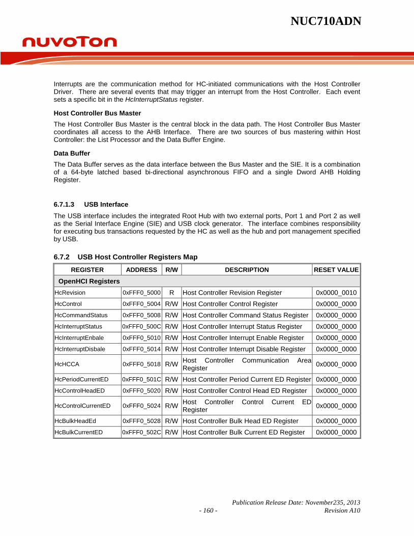
NUC710ADN
Publication Release Date: November235, 2013 - 160 - Revision A10
Interrupts are the communication method for HC-initiated communications with the Host Controller Driver. There are several events that may trigger an interrupt from the Host Controller. Each event sets a specific bit in the HcInterruptStatus register.
Host Controller Bus Master The Host Controller Bus Master is the central block in the data path. The Host Controller Bus Master coordinates all access to the AHB Interface. There are two sources of bus mastering within Host Controller: the List Processor and the Data Buffer Engine.
Data Buffer The Data Buffer serves as the data interface between the Bus Master and the SIE. It is a combination of a 64-byte latched based bi-directional asynchronous FIFO and a single Dword AHB Holding Register.
6.7.1.3 USB Interface The USB interface includes the integrated Root Hub with two external ports, Port 1 and Port 2 as well as the Serial Interface Engine (SIE) and USB clock generator. The interface combines responsibility for executing bus transactions requested by the HC as well as the hub and port management specified by USB.
6.7.2 USB Host Controller Registers Map
REGISTER ADDRESS R/W DESCRIPTION RESET VALUE
OpenHCI Registers HcRevision 0xFFF0_5000 R Host Controller Revision Register 0x0000_0010 HcControl 0xFFF0_5004 R/W Host Controller Control Register 0x0000_0000 HcCommandStatus 0xFFF0_5008 R/W Host Controller Command Status Register 0x0000_0000 HcInterruptStatus 0xFFF0_500C R/W Host Controller Interrupt Status Register 0x0000_0000 HcInterruptEnbale 0xFFF0_5010 R/W Host Controller Interrupt Enable Register 0x0000_0000 HcInterruptDisbale 0xFFF0_5014 R/W Host Controller Interrupt Disable Register 0x0000_0000
HcHCCA 0xFFF0_5018 R/W Host Controller Communication Area Register 0x0000_0000
HcPeriodCurrentED 0xFFF0_501C R/W Host Controller Period Current ED Register 0x0000_0000 HcControlHeadED 0xFFF0_5020 R/W Host Controller Control Head ED Register 0x0000_0000
HcControlCurrentED 0xFFF0_5024 R/W Host Controller Control Current ED Register 0x0000_0000
HcBulkHeadEd 0xFFF0_5028 R/W Host Controller Bulk Head ED Register 0x0000_0000 HcBulkCurrentED 0xFFF0_502C R/W Host Controller Bulk Current ED Register 0x0000_0000

NUC710ADN
Publication Release Date: November23, 2013 - 161 - Revision A10
Continued.
REGISTER ADDRESS R/W DESCRIPTION RESET VALUE
OpenHCI Registers HcDoneHeadED 0xFFF0_5030 R/W Host Controller Done Head Register 0x0000_0000 HcFmInterval 0xFFF0_5034 R/W Host Controller Frame Interval Register 0x0000_2EDF HcFrameRemaining 0xFFF0_5038 R Host Controller Frame Remaining Register 0x0000_0000 HcFmNumber 0xFFF0_503C R Host Controller Frame Number Register 0x0000_0000 HcPeriodicStart 0xFFF0_5040 R/W Host Controller Periodic Start Register 0x0000_0000
HcLSThreshold 0xFFF0_5044 R/W Host Controller Low Speed Threshold Register 0x0000_0628
HcRhDescriptorA 0xFFF0_5048 R/W Host Controller Root Hub Descriptor A Register 0x0100_0002
HcRhDescriptorB 0xFFF0_504C R/W Host Controller Root Hub Descriptor B Register 0x0000_0000
HcRhStatus 0xFFF0_5050 R/W Host Controller Root Hub Status Register 0x0000_0000 HcRhPortStatus [1] 0xFFF0_5054 R/W Host Controller Root Hub Port Status [1] 0x0000_0000 HcRhPortStatus [2] 0xFFF0_5058 R/W Host Controller Root Hub Port Status [2] 0x0000_0000
USB Configuration Registers TestModeEnable 0xFFF0_5200 R/W USB Test Mode Enable Register 0x0XXX_XXXX OperationalModeEnable 0xFFF0_5204 R/W USB Operational Mode Enable Register 0x0000_0000

NUC710ADN
Publication Release Date: November235, 2013 - 162 - Revision A10
Host Controller Revision Register
REGISTER OFFSET ADDRESS R/W DESCRIPTION RESET
VALUE HcRevision 0xFFF0_5000 R Host Controller Revision Register 0x0000_0010
31 30 29 28 27 26 25 24 Reserved
23 22 21 20 19 18 17 16 Reserved
15 14 13 12 11 10 9 8 Reserved
7 6 5 4 3 2 1 0 Revision
BITS DESCRIPTION
[31:8] Reserved Reserved. Read/Write 0's
[7:0] Revision Indicates the Open HCI Specification revision number implemented by the Hardware. Host Controller supports 1.0 specification. (X.Y = XYh)
Host Controller Control Register
REGISTER ADDRESS R/W DESCRIPTION RESET VALUE HcControl 0xFFF0_5004 R/W Host Controller Control Register 0x0000_0000
31 30 29 28 27 26 25 24 Reserved
23 22 21 20 19 18 17 16 Reserved
15 14 13 12 11 10 9 8 Reserved RWCE RWC IR
7 6 5 4 3 2 1 0 HCFS BLE CLE ISE PLE CBR
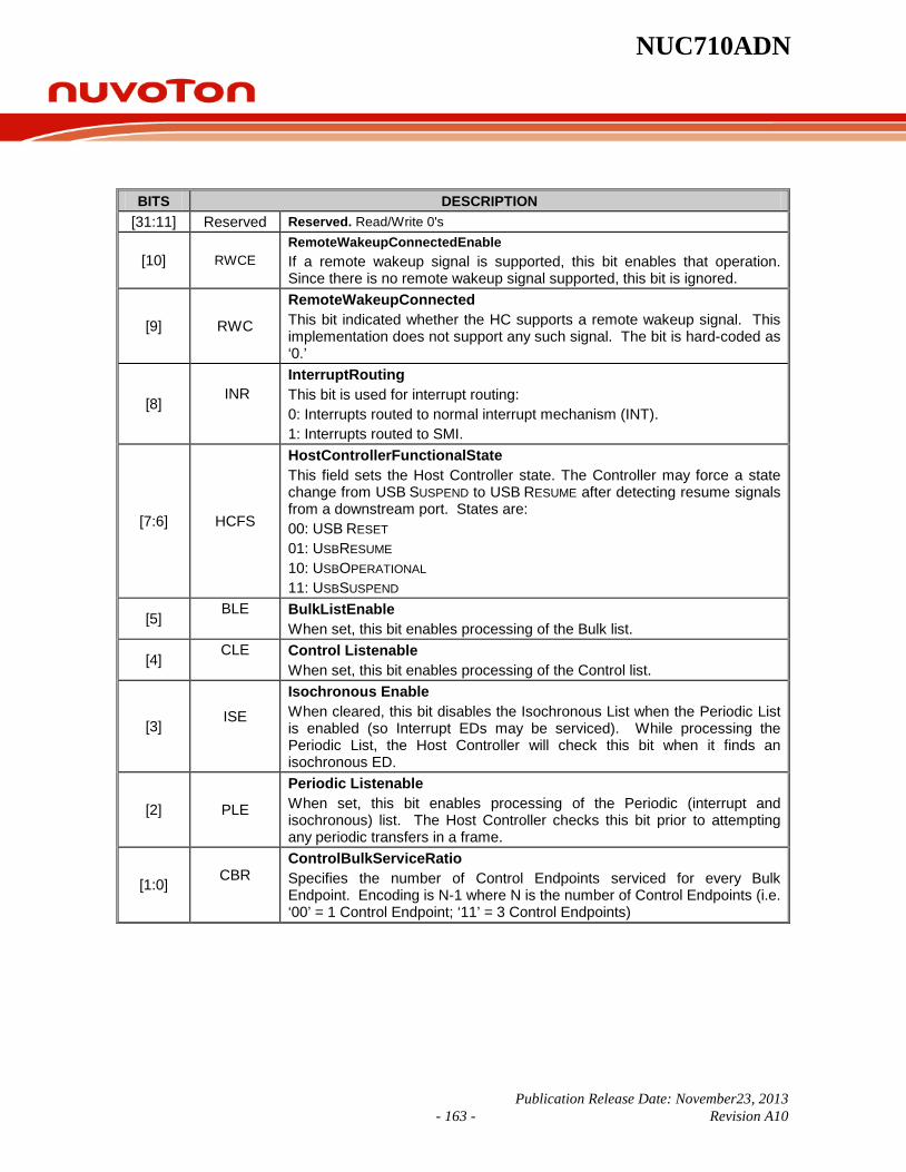
NUC710ADN
Publication Release Date: November23, 2013 - 163 - Revision A10
BITS DESCRIPTION [31:11] Reserved Reserved. Read/Write 0's
[10] RWCE RemoteWakeupConnectedEnable If a remote wakeup signal is supported, this bit enables that operation. Since there is no remote wakeup signal supported, this bit is ignored.
[9] RWC
RemoteWakeupConnected This bit indicated whether the HC supports a remote wakeup signal. This implementation does not support any such signal. The bit is hard-coded as ‘0.’
[8] INR
InterruptRouting This bit is used for interrupt routing: 0: Interrupts routed to normal interrupt mechanism (INT). 1: Interrupts routed to SMI.
[7:6] HCFS
HostControllerFunctionalState This field sets the Host Controller state. The Controller may force a state change from USB SUSPEND to USB RESUME after detecting resume signals from a downstream port. States are: 00: USB RESET 01: USBRESUME 10: USBOPERATIONAL 11: USBSUSPEND
[5] BLE
BulkListEnable When set, this bit enables processing of the Bulk list.
[4] CLE
Control Listenable When set, this bit enables processing of the Control list.
[3] ISE
Isochronous Enable When cleared, this bit disables the Isochronous List when the Periodic List is enabled (so Interrupt EDs may be serviced). While processing the Periodic List, the Host Controller will check this bit when it finds an isochronous ED.
[2] PLE
Periodic Listenable When set, this bit enables processing of the Periodic (interrupt and isochronous) list. The Host Controller checks this bit prior to attempting any periodic transfers in a frame.
[1:0] CBR
ControlBulkServiceRatio Specifies the number of Control Endpoints serviced for every Bulk Endpoint. Encoding is N-1 where N is the number of Control Endpoints (i.e. ‘00’ = 1 Control Endpoint; ‘11’ = 3 Control Endpoints)
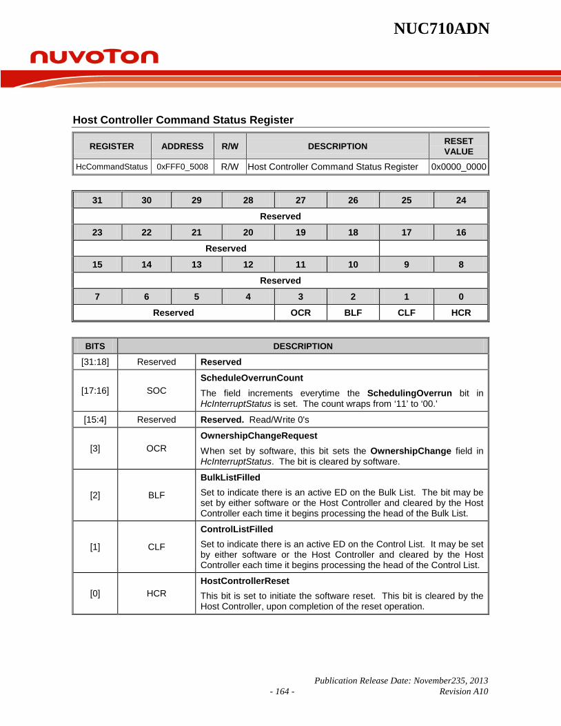
NUC710ADN
Publication Release Date: November235, 2013 - 164 - Revision A10
Host Controller Command Status Register
REGISTER ADDRESS R/W DESCRIPTION RESET VALUE
HcCommandStatus 0xFFF0_5008 R/W Host Controller Command Status Register 0x0000_0000
31 30 29 28 27 26 25 24
Reserved
23 22 21 20 19 18 17 16
Reserved
15 14 13 12 11 10 9 8
Reserved
7 6 5 4 3 2 1 0
Reserved OCR BLF CLF HCR
BITS DESCRIPTION
[31:18] Reserved Reserved
[17:16] SOC ScheduleOverrunCount The field increments everytime the SchedulingOverrun bit in HcInterruptStatus is set. The count wraps from ‘11’ to ‘00.’
[15:4] Reserved Reserved. Read/Write 0's
[3] OCR OwnershipChangeRequest When set by software, this bit sets the OwnershipChange field in HcInterruptStatus. The bit is cleared by software.
[2] BLF
BulkListFilled Set to indicate there is an active ED on the Bulk List. The bit may be set by either software or the Host Controller and cleared by the Host Controller each time it begins processing the head of the Bulk List.
[1] CLF
ControlListFilled Set to indicate there is an active ED on the Control List. It may be set by either software or the Host Controller and cleared by the Host Controller each time it begins processing the head of the Control List.
[0] HCR HostControllerReset This bit is set to initiate the software reset. This bit is cleared by the Host Controller, upon completion of the reset operation.

NUC710ADN
Publication Release Date: November23, 2013 - 165 - Revision A10
Host Controller Interrupt Status Register All bits are set by hardware and cleared by software.
REGISTER ADDRESS R/W DESCRIPTION RESET VALUE
HcInterruptStatus 0xFFF0_500C R/W Host Controller Interrupt Status Register 0x0000_0000
31 30 29 28 27 26 25 24
Reserve
OCH Reserved 23 22 21 20 19 18 17 16
Reserved 15 14 13 12 11 10 9 8
Reserved 7 6 5 4 3 2 1 0
Reserve
RHSC FNO URE RDT SOF WDH SCO
BITS DESCRIPTION [31] Reserved Reserved
[30] OCH OwnershipChange This bit is set when the OwnershipChangeRequest bit of HcCommandStatus is set.
[29:7] Reserved
[6] RHSC RootHubStatusChange This bit is set when the content of HcRhStatus or the content of any HcRhPortStatus register has changed.
[5] FNO FrameNumberOverflow Set when bit 15 of FrameNumber changes value.
[4] URE UnrecoverableError This event is not implemented and is hard-coded to ‘0.’ Writes are ignored.
[3] RDT ResumeDetected Set when Host Controller detects resume signaling on a downstream port.
[2] SOF StartOfFrame Set when the Frame Management block signals a ‘Start of Frame’ event.
[1] WDH WritebackDoneHead Set after the Host Controller has written HcDoneHead to HccaDoneHead.
[0] SCHO SchedulingOverrun Set when the List Processor determines a Schedule Overrun has occurred.

NUC710ADN
Publication Release Date: November235, 2013 - 166 - Revision A10
Host Controller Interrupt Enable Register Writing 1 to a bit in this register sets the corresponding bit, while writing a 0 leaves the bit unchanged.
REGISTER ADDRESS R/W DESCRIPTION RESET VALUE
HcInterruptEnable 0xFFF0_5010 R/W Host Controller Interrupt Enable Register 0x0000_0000
31 30 29 28 27 26 25 24 MIE OCE Reserved 23 22 21 20 19 18 17 16
Reserved 15 14 13 12 11 10 9 8
Reserved 7 6 5 4 3 2 1 0
Reserved RHCE FNOE UREE RDTE SOFE WDHE SCHOE
BITS DESCRIPTION
[31] MIE MasterInterruptEnable This bit is a global interrupt enable. Writing 1 allows interrupts to be enabled via the specific enable bits listed above.
[30] OCE OwnershipChangeEnable 0: Ignore 1: Enable interrupt generation due to Ownership Change.
[29:7] Reserved Reserved. Read/Write 0's
[6] RHSCE RootHubStatusChangeEnable 0: Ignore 1: Enable interrupt generation due to Root Hub Status Change.
[5] FNOE FrameNumberOverflowEnable 0: Ignore 1: Enable interrupt generation due to Frame Number Overflow.
[4] UREE UnrecoverableErrorEnable This event is not implemented. All writes to this bit are ignored.
[3] RDTE ResumeDetectedEnable 0: Ignore 1: Enable interrupt generation due to Resume Detected.
[2] SOFE StartOfFrameEnable 0: Ignore 1: Enable interrupt generation due to Start of Frame.
[1] WDHE WritebackDoneHeadEnable 0: Ignore 1: Enable interrupt generation due to Write-back Done Head.

NUC710ADN
Publication Release Date: November23, 2013 - 167 - Revision A10
Continued.
BITS DESCRIPTION
[0] SCHOE SchedulingOverrunEnable 0: Ignore 1: Enable interrupt generation due to Scheduling Overrun.
Host Controller Interrupt Disable Register Writing 1 to a bit in this register clears the corresponding bit, while writing 0 leaves that bit unchanged.
REGISTER ADDRESS R/W DESCRIPTION RESET VALUE
HcInterruptEnable 0xFFF0_5014 R/W Host Controller Interrupt Disable Register 0x0000_0000
31 30 29 28 27 26 25 24
MIE OCE Reserved
23 22 21 20 19 18 17 16
Reserved
15 14 13 12 11 10 9 8
Reserved
7 6 5 4 3 2 1 0
Reserved RHSCE FNOE UREE RDTE SOFE WDHE SCHOE
BITS DESCRIPTION
[31] MIE MasterInterruptEnable Global interrupt disable. Writing 1 disables all interrupts.
[30] OCE OwnershipChangeEnable 0: Ignore 1: Disable interrupt generation due to Ownership Change.
[29:7] Reserved Reserved. Read/Write 0's
[6] RHSCE RootHubStatusChangeEnable 0: Ignore 1: Disable interrupt generation due to Root Hub Status Change.
[5] FNOE FrameNumberOverflowEnable 0: Ignore 1: Disable interrupt generation due to Frame Number Overflow.

NUC710ADN
Publication Release Date: November235, 2013 - 168 - Revision A10
Continued
BITS DESCRIPTION
[4] UREE UnrecoverableErrorEnable This event is not implemented. All writes to this bit are ignored.
[3] RDTE ResumeDetectedEnable 0: Ignore 1: Disable interrupt generation due to Resume Detected.
[2] SOFE StartOfFrameEnable 0: Ignore 1: Disable interrupt generation due to Start of Frame.
[1] WDHE WritebackDoneHeadEnable 0: Ignore 1: Disable interrupt generation due to Write-back Done Head.
[0] SCHOE SchedulingOverrunEnable 0: Ignore 1: Disable interrupt generation due to Scheduling Overrun.
Host Controller Communication Area Register
REGISTER ADDRESS R/W DESCRIPTION RESET VALUE
HcHCCA 0xFFF0_5018 R/W Host Controller Communication Area Register 0x0000_0000
31 30 29 28 27 26 25 24
HCCA 23 22 21 20 19 18 17 16
HCCA 15 14 13 12 11 10 9 8
HCCA 7 6 5 4 3 2 1 0
Reserved
BITS DESCRIPTION
[31:8] HCCA HCCA Pointer to HCCA base address.
[7:0] Reserved Reserved
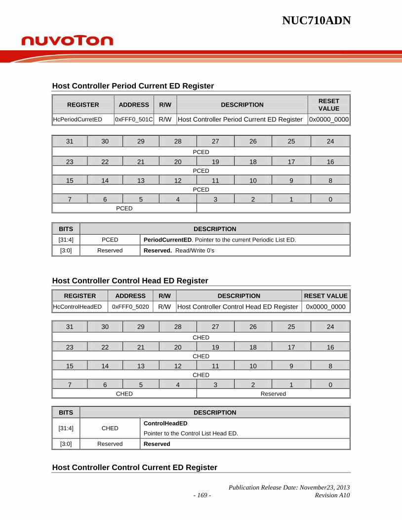
NUC710ADN
Publication Release Date: November23, 2013 - 169 - Revision A10
Host Controller Period Current ED Register
REGISTER ADDRESS R/W DESCRIPTION RESET VALUE
HcPeriodCurretED 0xFFF0_501C R/W Host Controller Period Current ED Register 0x0000_0000
31 30 29 28 27 26 25 24 PCED
23 22 21 20 19 18 17 16 PCED
15 14 13 12 11 10 9 8 PCED
7 6 5 4 3 2 1 0 PCED
BITS DESCRIPTION [31:4] PCED PeriodCurrentED. Pointer to the current Periodic List ED.
[3:0] Reserved Reserved. Read/Write 0's
Host Controller Control Head ED Register
REGISTER ADDRESS R/W DESCRIPTION RESET VALUE HcControlHeadED 0xFFF0_5020 R/W Host Controller Control Head ED Register 0x0000_0000
31 30 29 28 27 26 25 24 CHED
23 22 21 20 19 18 17 16 CHED
15 14 13 12 11 10 9 8 CHED
7 6 5 4 3 2 1 0 CHED Reserved
BITS DESCRIPTION
[31:4] CHED ControlHeadED
Pointer to the Control List Head ED.
[3:0] Reserved Reserved
Host Controller Control Current ED Register

NUC710ADN
Publication Release Date: November235, 2013 - 170 - Revision A10
REGISTER OFFSET ADDRESS R/W DESCRIPTION RESET
VALUE
HcControlCurrentED 0xFFF0_5024 R/W Host Controller Control Current ED Register 0x0000_0000
31 30 29 28 27 26 25 24 CCED
23 22 21 20 19 18 17 16 CCED
15 14 13 12 11 10 9 8 CCED
7 6 5 4 3 2 1 0 CCED Reserved
BITS DESCRIPTION
[31:4] CCED ControlCurrentED
Pointer to the current Control List ED.
[3:0] Reserved Reserved. Read/Write 0's
Host Controller Bulk Head ED Register
REGISTER OFFSET ADDRESS R/W DESCRIPTION RESET
VALUE HcBulkHEADED 0xFFF0_5028 R/W Host Controller Bulk Head ED Register 0x0000_0000
31 30 29 28 27 26 25 24 BHED
23 22 21 20 19 18 17 16 BHED
15 14 13 12 11 10 9 8 BHED
7 6 5 4 3 2 1 0 BHED Reserved
BITS DESCRIPTION [31:4] BHED BulkHeadED. Pointer to the Bulk List Head ED.
[3:0] Reserved Reserved. Read/Write 0's

NUC710ADN
Publication Release Date: November23, 2013 - 171 - Revision A10
Host Controller Bulk Current ED Register
REGISTER OFFSET ADDRESS R/W DESCRIPTION RESET
VALUE HcBulkCurrentED 0xFFF0_502C R/W Host Controller Bulk Current ED Register 0x0000_0000
31 30 29 28 27 26 25 24 BCED
23 22 21 20 19 18 17 16 BCED
15 14 13 12 11 10 9 8 BCED
7 6 5 4 3 2 1 0 BCED Reserved
BITS DESCRIPTION [31:4] BCED BulkCurrentED. Pointer to the current Bulk List ED.
[3:0] Reserved Reserved. Read/Write 0's
Host Controller Done Head Register
REGISTER ADDRESS R/W DESCRIPTION RESET VALUE
HcDoneHead 0xFFF0_5030 R/W Host Controller Done Head Register 0x0000_0000
31 30 29 28 27 26 25 24 DOHD
23 22 21 20 19 18 17 16 DOHD
15 14 13 12 11 10 9 8 DOHD
7 6 5 4 3 2 1 0 DOHD Reserved
BITS DESCRIPTION [31:4] DOHD DoneHead. Pointer to the current Done List Head ED.
[3:0] Reserved Reserved. Read/Write 0's
Host Controller Frame Interval Register

NUC710ADN
Publication Release Date: November235, 2013 - 172 - Revision A10
REGISTER ADDRESS R/W DESCRIPTION RESET VALUE
HcFmInterval 0xFFF0_5034 R/W Host Controller Frame Interval Register 0x0000_2EDF
31 30 29 28 27 26 25 24 FINTVT FSLDP
23 22 21 20 19 18 17 16 FSLDP
15 14 13 12 11 10 9 8 Reserved FINTV
7 6 5 4 3 2 1 0 FINTV
BITS DESCRIPTION
31 FINTVT FrameIntervalToggle
This bit is toggled by HCD when it loads a new value into Frame Interval.
[30:16] FSLDP FSLargestDataPacket This field specifies a value that is loaded into the Largest Data Packet Counter at the beginning of each frame.
[15:14] Reserved Reserved. Read/Write 0's
[13:0] FINTV Frame Interval This field specifies the length of a frame as (bit times - 1). For 12,000 bit times in a frame, a value of 11,999 is stored here.
Host Controller Frame Remaining Register
REGISTER ADDRESS R/W DESCRIPTION RESET VALUE
HcFmInterval 0xFFF0_5038 R Host Controller Frame Remaining Register 0x0000_0000
31 30 29 28 27 26 25 24 FRMT Reserved
23 22 21 20 19 18 17 16 Reserved
15 14 13 12 11 10 9 8 Reserved FRM
7 6 5 4 3 2 1 0 FRM
BITS DESCRIPTION
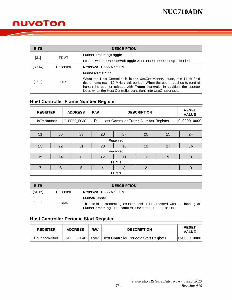
NUC710ADN
Publication Release Date: November23, 2013 - 173 - Revision A10
BITS DESCRIPTION
[31] FRMT FrameRemainingToggle
Loaded with FrameIntervalToggle when Frame Remaining is loaded.
[30:14] Reserved Reserved. Read/Write 0's
[13:0] FRM
Frame Remaining
When the Host Controller is in the USBOPERATIONAL state, this 14-bit field decrements each 12 MHz clock period. When the count reaches 0, (end of frame) the counter reloads with Frame Interval. In addition, the counter loads when the Host Controller transitions into USBOPERATIONAL.
Host Controller Frame Number Register
REGISTER ADDRESS R/W DESCRIPTION RESET VALUE
HcFmNumber 0xFFF0_503C R Host Controller Frame Number Register 0x0000_0000
31 30 29 28 27 26 25 24 Reserved
23 22 21 20 19 18 17 16 Reserved
15 14 13 12 11 10 9 8 FRMN
7 6 5 4 3 2 1 0 FRMN
BITS DESCRIPTION [31:16] Reserved Reserved. Read/Write 0's
[15:0] FRMN FrameNumber This 16-bit incrementing counter field is incremented with the loading of FrameRemaining. The count rolls over from ‘FFFFh’ to ‘0h.’
Host Controller Periodic Start Register
REGISTER ADDRESS R/W DESCRIPTION RESET VALUE
HcPeriodicStart 0xFFF0_5040 R/W Host Controller Periodic Start Register 0x0000_0000
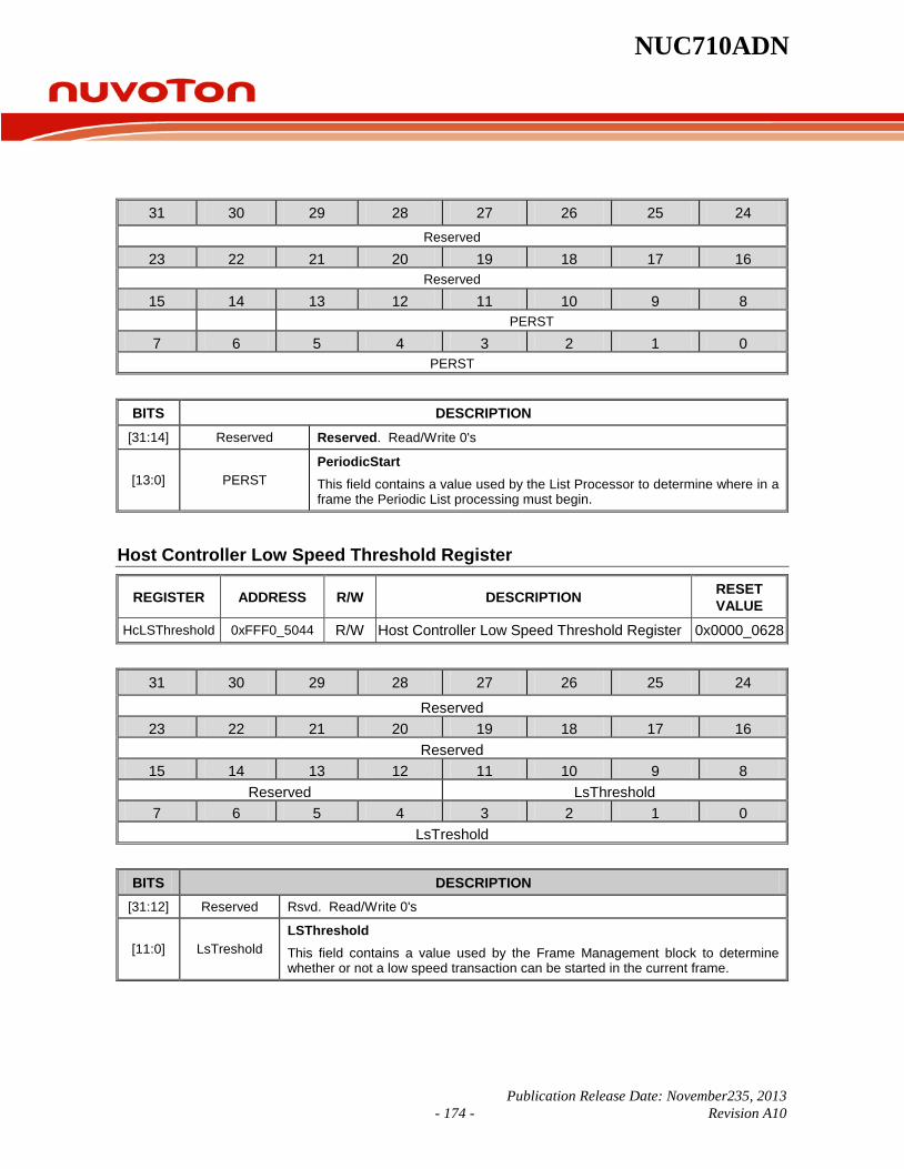
NUC710ADN
Publication Release Date: November235, 2013 - 174 - Revision A10
31 30 29 28 27 26 25 24 Reserved
23 22 21 20 19 18 17 16 Reserved
15 14 13 12 11 10 9 8 PERST 7 6 5 4 3 2 1 0
PERST
BITS DESCRIPTION [31:14] Reserved Reserved. Read/Write 0's
[13:0] PERST PeriodicStart This field contains a value used by the List Processor to determine where in a frame the Periodic List processing must begin.
Host Controller Low Speed Threshold Register
REGISTER ADDRESS R/W DESCRIPTION RESET VALUE
HcLSThreshold 0xFFF0_5044 R/W Host Controller Low Speed Threshold Register 0x0000_0628
31 30 29 28 27 26 25 24
Reserved 23 22 21 20 19 18 17 16
Reserved 15 14 13 12 11 10 9 8
Reserved LsThreshold 7 6 5 4 3 2 1 0
LsTreshold
BITS DESCRIPTION [31:12] Reserved Rsvd. Read/Write 0's
[11:0] LsTreshold LSThreshold
This field contains a value used by the Frame Management block to determine whether or not a low speed transaction can be started in the current frame.
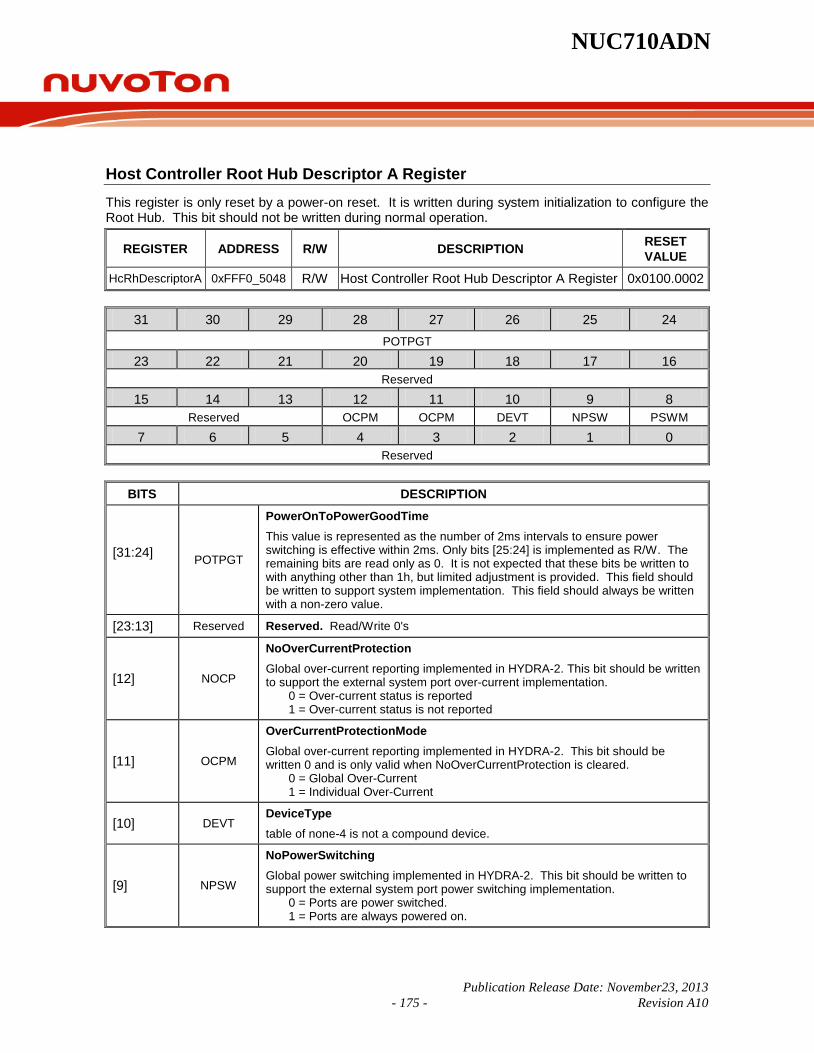
NUC710ADN
Publication Release Date: November23, 2013 - 175 - Revision A10
Host Controller Root Hub Descriptor A Register This register is only reset by a power-on reset. It is written during system initialization to configure the Root Hub. This bit should not be written during normal operation.
REGISTER ADDRESS R/W DESCRIPTION RESET VALUE
HcRhDescriptorA 0xFFF0_5048 R/W Host Controller Root Hub Descriptor A Register 0x0100.0002
31 30 29 28 27 26 25 24 POTPGT
23 22 21 20 19 18 17 16 Reserved
15 14 13 12 11 10 9 8 Reserved OCPM OCPM DEVT NPSW PSWM
7 6 5 4 3 2 1 0 Reserved
BITS DESCRIPTION
[31:24] POTPGT
PowerOnToPowerGoodTime
This value is represented as the number of 2ms intervals to ensure power switching is effective within 2ms. Only bits [25:24] is implemented as R/W. The remaining bits are read only as 0. It is not expected that these bits be written to with anything other than 1h, but limited adjustment is provided. This field should be written to support system implementation. This field should always be written with a non-zero value.
[23:13] Reserved Reserved. Read/Write 0's
[12] NOCP
NoOverCurrentProtection Global over-current reporting implemented in HYDRA-2. This bit should be written to support the external system port over-current implementation. 0 = Over-current status is reported 1 = Over-current status is not reported
[11] OCPM
OverCurrentProtectionMode Global over-current reporting implemented in HYDRA-2. This bit should be written 0 and is only valid when NoOverCurrentProtection is cleared. 0 = Global Over-Current 1 = Individual Over-Current
[10] DEVT DeviceType table of none-4 is not a compound device.
[9] NPSW
NoPowerSwitching Global power switching implemented in HYDRA-2. This bit should be written to support the external system port power switching implementation. 0 = Ports are power switched. 1 = Ports are always powered on.
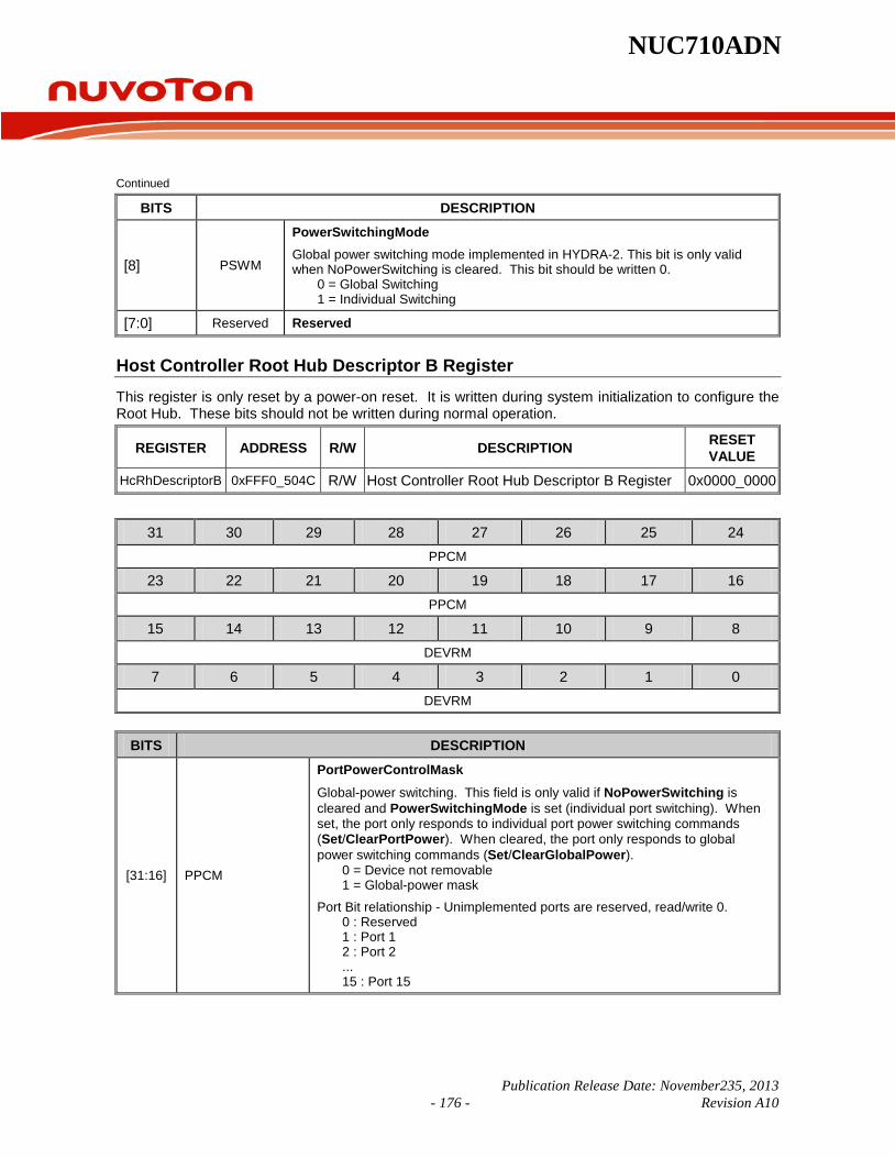
NUC710ADN
Publication Release Date: November235, 2013 - 176 - Revision A10
Continued
BITS DESCRIPTION
[8] PSWM
PowerSwitchingMode Global power switching mode implemented in HYDRA-2. This bit is only valid when NoPowerSwitching is cleared. This bit should be written 0. 0 = Global Switching 1 = Individual Switching
[7:0] Reserved Reserved
Host Controller Root Hub Descriptor B Register This register is only reset by a power-on reset. It is written during system initialization to configure the Root Hub. These bits should not be written during normal operation.
REGISTER ADDRESS R/W DESCRIPTION RESET VALUE
HcRhDescriptorB 0xFFF0_504C R/W Host Controller Root Hub Descriptor B Register 0x0000_0000
31 30 29 28 27 26 25 24 PPCM
23 22 21 20 19 18 17 16 PPCM
15 14 13 12 11 10 9 8 DEVRM
7 6 5 4 3 2 1 0 DEVRM
BITS DESCRIPTION
[31:16] PPCM
PortPowerControlMask
Global-power switching. This field is only valid if NoPowerSwitching is cleared and PowerSwitchingMode is set (individual port switching). When set, the port only responds to individual port power switching commands (Set/ClearPortPower). When cleared, the port only responds to global power switching commands (Set/ClearGlobalPower). 0 = Device not removable 1 = Global-power mask
Port Bit relationship - Unimplemented ports are reserved, read/write 0. 0 : Reserved 1 : Port 1 2 : Port 2 ... 15 : Port 15

NUC710ADN
Publication Release Date: November23, 2013 - 177 - Revision A10
Continued
BITS DESCRIPTION
[15:0] DEVRM
DeviceRemoveable table of none-4 ports default to removable devices. 0 = Device not removable 1 = Device removable
Port Bit relationship 0 : Reserved 1 : Port 1 2 : Port 2 ... 15 : Port 15
Unimplemented ports are reserved, read/write 0.
Host Controller Root Hub Status Register This register is reset by the USBRESET state.
REGISTER ADDRESS R/W DESCRIPTION RESET VALUE
HcRhStstus 0xFFF0_5050 R/W Host Controller Root Hub Status Register 0x0000_0000
31 30 29 28 27 26 25 24
Reserved 23 22 21 20 19 18 17 16
Reserved OVIC LPSC 15 14 13 12 11 10 9 8
DRWE PDWKS2 PDWKS1 Reserved 7 6 5 4 3 2 1 0
Reserved OVRCI LOPS
BITS DESCRIPTION
[31] CRWE (Write) ClearRemoteWakeupEnable Writing 1 to this bit clears DeviceRemoteWakeupEnable. Writing 1 has no effect.
[30:18] Reserved Reserved. Read/Write 0's
[17] OVIC OverCurrentIndicatorChange This bit is set when OverCurrentIndicator changes. Writing 1 clears this bit. Writing 0 has no effect.
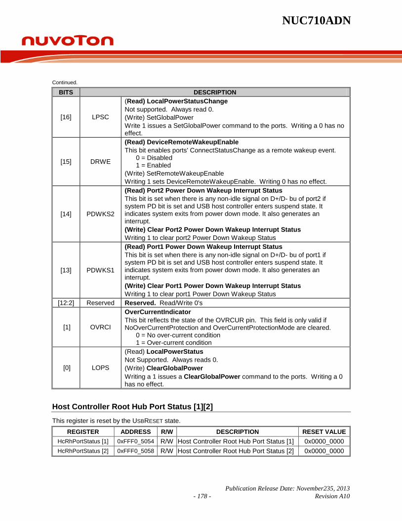
NUC710ADN
Publication Release Date: November235, 2013 - 178 - Revision A10
Continued.
BITS DESCRIPTION
[16] LPSC
(Read) LocalPowerStatusChange Not supported. Always read 0. (Write) SetGlobalPower Write 1 issues a SetGlobalPower command to the ports. Writing a 0 has no effect.
[15] DRWE
(Read) DeviceRemoteWakeupEnable This bit enables ports' ConnectStatusChange as a remote wakeup event. 0 = Disabled 1 = Enabled (Write) SetRemoteWakeupEnable Writing 1 sets DeviceRemoteWakeupEnable. Writing 0 has no effect.
[14] PDWKS2
(Read) Port2 Power Down Wakeup Interrupt Status This bit is set when there is any non-idle signal on D+/D- bu of port2 if system PD bit is set and USB host controller enters suspend state. It indicates system exits from power down mode. It also generates an interrupt. (Write) Clear Port2 Power Down Wakeup Interrupt Status Writing 1 to clear port2 Power Down Wakeup Status
[13] PDWKS1
(Read) Port1 Power Down Wakeup Interrupt Status This bit is set when there is any non-idle signal on D+/D- bu of port1 if system PD bit is set and USB host controller enters suspend state. It indicates system exits from power down mode. It also generates an interrupt. (Write) Clear Port1 Power Down Wakeup Interrupt Status Writing 1 to clear port1 Power Down Wakeup Status
[12:2] Reserved Reserved. Read/Write 0's
[1] OVRCI
OverCurrentIndicator This bit reflects the state of the OVRCUR pin. This field is only valid if NoOverCurrentProtection and OverCurrentProtectionMode are cleared. 0 = No over-current condition 1 = Over-current condition
[0] LOPS
(Read) LocalPowerStatus Not Supported. Always reads 0. (Write) ClearGlobalPower Writing a 1 issues a ClearGlobalPower command to the ports. Writing a 0 has no effect.
Host Controller Root Hub Port Status [1][2] This register is reset by the USBRESET state.
REGISTER ADDRESS R/W DESCRIPTION RESET VALUE HcRhPortStatus [1] 0xFFF0_5054 R/W Host Controller Root Hub Port Status [1] 0x0000_0000 HcRhPortStatus [2] 0xFFF0_5058 R/W Host Controller Root Hub Port Status [2] 0x0000_0000

NUC710ADN
Publication Release Date: November23, 2013 - 179 - Revision A10
31 30 29 28 27 26 25 24 Reserved
23 22 21 20 19 18 17 16 Reserved PRSC POCIC PSSC PESC CSC
15 14 13 12 11 10 9 8 Reserved LSDA PPS
7 6 5 4 3 2 1 0 Reserved SPR CPS SPS SPE DRM
BITS DESCRIPTION [31:21] Reserved Reserved. Read/Write 0's
[20] PRSC
PortResetStatusChange
This bit indicates that the port-reset signal is complete. 0 = Port reset is not complete. 1 = Port reset is complete.
[19] POCIC PortOverCurrentIndicatorChange
This bit is set when OverCurrentIndicator changes. Writing 1 clears this bit. Writing a 0 has no effect.
[18] PSSC
PortSuspendStatusChange
This bit indicates the completion of the selective resume sequence for the port. 0 = Port is not resumed. 1 = Port resume is complete.
[17] PESC
PortEnableStatusChange
This bit indicates that the port has been disabled due to a hardware event (cleared PortEnableStatus). 0 = Port has not been disabled. 1 = PortEnableStatus has been cleared.
[16] CSC
ConnectStatusChange
This bit indicates connect or disconnect event has been detected. Writing 1 clears this bit. Writing 0 has no effect. 0 = No connect/disconnect event. 1 = Hardware detection of connect/disconnect event.
Note: If DeviceRemoveable is set, this bit resets to 1.
[15:10] Reserved Reserved. Read/Write 0's
[9] LSDA
(Read) LowSpeedDeviceAttached
This bit defines the speed (and bud idle) of the attached device. It is only valid when CurrentConnectStatus is set. 0 = Full Speed device 1 = Low Speed device
(Write) ClearPortPower Writing 1 clears PortPowerStatus. Writing a 0 has no effect
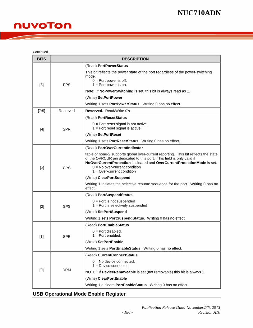
NUC710ADN
Publication Release Date: November235, 2013 - 180 - Revision A10
Continued.
BITS DESCRIPTION
[8] PPS
(Read) PortPowerStatus
This bit reflects the power state of the port regardless of the power-switching mode. 0 = Port power is off. 1 = Port power is on.
Note: If NoPowerSwitching is set, this bit is always read as 1.
(Write) SetPortPower Writing 1 sets PortPowerStatus. Writing 0 has no effect.
[7:5] Reserved Reserved. Read/Write 0's
[4] SPR
(Read) PortResetStatus
0 = Port reset signal is not active. 1 = Port reset signal is active.
(Write) SetPortReset Writing 1 sets PortResetStatus. Writing 0 has no effect.
[3] CPS
(Read) PortOverCurrentIndicator table of none-2 supports global over-current reporting. This bit reflects the state of the OVRCUR pin dedicated to this port. This field is only valid if NoOverCurrentProtection is cleared and OverCurrentProtectionMode is set. 0 = No over-current condition 1 = Over-current condition
(Write) ClearPortSuspend
Writing 1 initiates the selective resume sequence for the port. Writing 0 has no effect.
[2] SPS
(Read) PortSuspendStatus
0 = Port is not suspended 1 = Port is selectively suspended
(Write) SetPortSuspend
Writing 1 sets PortSuspendStatus. Writing 0 has no effect.
[1] SPE
(Read) PortEnableStatus 0 = Port disabled. 1 = Port enabled.
(Write) SetPortEnable
Writing 1 sets PortEnableStatus. Writing 0 has no effect.
[0] DRM
(Read) CurrentConnectStatus
0 = No device connected. 1 = Device connected.
NOTE: If DeviceRemoveable is set (not removable) this bit is always 1.
(Write) ClearPortEnable
Writing 1 a clears PortEnableStatus. Writing 0 has no effect.
USB Operational Mode Enable Register

NUC710ADN
Publication Release Date: November23, 2013 - 181 - Revision A10
This register selects which operational mode is enabled. Bits defined as write-only are read as 0's.
REGISTER ADDRESS R/W DESCRIPTION RESET VALUE
OperationalModeEnable 0xFFF0_5204 R/W USB Operational Mode Enable Register 0x0000_0000
31 30 29 28 27 26 25 24 Reserved
23 22 21 20 19 18 17 16 Reserved
15 14 13 12 11 10 9 8 Reserved SIEPD
7 6 5 4 3 2 1 0 Reserved OVRCUR
Reserved DBREG
BITS BIT DESCRIPTION [31:9] Reserved Reserved. Read/write 0
[8] SIEPD
SIE Pipeline Disable When set, waits for all USB bus activity to complete prior to returning completion status to the List Processor. This is a failsafe mechanism to avoid potential problems with the clk_dr transition between 1.5 MHz and 12 MHz.
[7:4] Reserved Reserved. Read/write 0
[3] OVRCURP
OVRCURP (over current indicator polarity) When the OVRCURP bit is clear, the OVRCUR non-inverted to input into USB host controller. In contrast, when the OVRCURP bit is set, the OVRCUR inverted to input into USB host controller.
[2:1] Reserved Reserved. Read/write 0
[0] DBREG Data Buffer Region 16 When set, the size of the data buffer region is 16 bytes. Otherwise, the size is 32 bytes.
6.7.3 HCCA
6.7.4 Endpoint Descriptor
6.7.5 Transfer Descriptor
6.8 USB Device Controller The USB controller interfaces the AHB bus and the USB bus. The USB controller contains both the AHB master interface and AHB slave interface. The CPU programs the USB controller through the AHB slave interface. For IN or OUT transfers, the USB controller needs to write data to memory or read data from memory through the AHB master interface. The USB controller also contains the USB transceiver to interface the USB.

NUC710ADN
Publication Release Date: November235, 2013 - 182 - Revision A10
6.8.1 USB Endpoints
Consists of four endpoints, designated EP0, EPA, EPB and EPC. Each is intended for a particular use as described below:
EP0: the default endpoint uses control transfer (In/Out) to handle configuration and control functions required by the USB specification. Maximum packed size is 16 bytes.
EPA: designed as a general endpoint. This endpoint could be programmed to be an Interrupt IN endpoint or an Isochronous IN endpoint or a Bulk In endpoint or Bulk OUT endpoint.
EPB: designed as a general endpoint. This endpoint could be programmed to be an Interrupt IN endpoint or an Isochronous IN endpoint or a Bulk In endpoint or Bulk OUT endpoint.
EPC: designed as a general endpoint. This endpoint could be programmed to be an Interrupt IN endpoint or an Isochronous IN endpoint or a Bulk In endpoint or Bulk OUT endpoint.
6.8.2 Standard device request
USB controller has built-in hard-wired state machine to automatically respond to USB standard device requests. It also supports detecting class and vendor requests. For Get Descriptor request and Class or Vendor command, the firmware will control these procedures.
6.8.3 USB Device Register Description
USB Control Register (USB_CTL)
REGISTER ADDRESS R/W DESCRIPTION RESET VALUE
USB_CTL 0xFFF0_6000 R/W USB control register 0x0000_0000
31 30 29 28 27 26 25 24
Reserved 23 22 21 20 19 18 17 16
Reserved
15 14 13 12 11 10 9 8
Reserved WakeUp
7 6 5 4 3 2 1 0
CCMD VCMD SIE_RCV SUS_TST RWU_EN SUSP USB_RST USB_EN
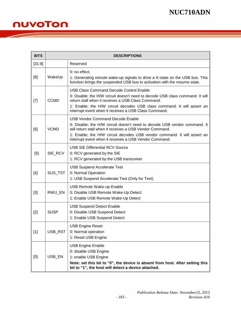
NUC710ADN
Publication Release Date: November23, 2013 - 183 - Revision A10
BITS DESCRIPTIONS
[31:9] Reserved
[8] WakeUp 0: no effect. 1: Generating remote wake-up signals to drive a K-state on the USB bus. This function brings the suspended USB bus to activation with the resume state.
[7] CCMD
USB Class Command Decode Control Enable 0: Disable; the H/W circuit doesn’t need to decode USB class command. It will return stall when it receives a USB Class Command. 1: Enable; the H/W circuit decodes USB class command. It will assert an interrupt event when it receives a USB Class Command.
[6] VCMD
USB Vendor Command Decode Enable 0: Disable; the H/W circuit doesn’t need to decode USB vendor command. It will return stall when it receives a USB Vendor Command. 1: Enable; the H/W circuit decodes USB vendor command. It will assert an interrupt event when it receives a USB Vendor Command.
[5] SIE_RCV USB SIE Differential RCV Source 0: RCV generated by the SIE 1: RCV generated by the USB transceiver
[4] SUS_TST USB Suspend Accelerate Test 0: Normal Operation 1: USB Suspend Accelerate Test (Only for Test)
[3] RWU_EN USB Remote Wake-up Enable 0: Disable USB Remote Wake-Up Detect 1: Enable USB Remote Wake-Up Detect
[2] SUSP USB Suspend Detect Enable 0: Disable USB Suspend Detect 1: Enable USB Suspend Detect
[1] USB_RST USB Engine Reset 0: Normal operation 1: Reset USB Engine
[0] USB_EN
USB Engine Enable 0: disable USB Engine 1: enable USB Engine Note: set this bit to “0”, the device is absent from host. After setting this bit to “1”, the host will detect a device attached.
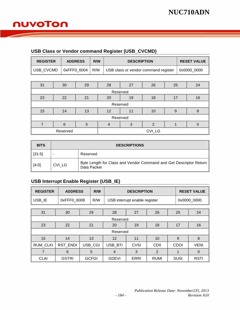
NUC710ADN
Publication Release Date: November235, 2013 - 184 - Revision A10
USB Class or Vendor command Register (USB_CVCMD)
REGISTER ADDRESS R/W DESCRIPTION RESET VALUE
USB_CVCMD 0xFFF0_6004 R/W USB class or vendor command register 0x0000_0000
31 30 29 28 27 26 25 24
Reserved 23 22 21 20 19 18 17 16
Reserved
15 14 13 12 11 10 9 8
Reserved
7 6 5 4 3 2 1 0
Reserved CVI_LG
BITS DESCRIPTIONS
[31:5] - Reserved
[4:0] CVI_LG Byte Length for Class and Vendor Command and Get Descriptor Return Data Packet
USB Interrupt Enable Register (USB_IE)
REGISTER ADDRESS R/W DESCRIPTION RESET VALUE
USB_IE 0xFFF0_6008 R/W USB interrupt enable register 0x0000_0000
31 30 29 28 27 26 25 24
Reserved 23 22 21 20 19 18 17 16
Reserved
15 14 13 12 11 10 9 8
RUM_CLKI RST_ENDI USB_CGI USB_BTI CVSI CDII CDOI VENI
7 6 5 4 3 2 1 0
CLAI GSTRI GCFGI GDEVI ERRI RUMI SUSI RSTI

NUC710ADN
Publication Release Date: November23, 2013 - 185 - Revision A10
BITS DESCRIPTIONS
[31:16] - Reserved
[15] RUM_CLKI Interrupt enable for RESUME (if clock is stopped) 0: Disable 1: Enable
[14] RST_ENDI Interrupt enable for USB reset end 0: Disable 1: Enable
[13] USB_CGI
Interrupt Enable for Device Configured 0: Disable 1: Enable Note: the interrupt occurs when the device configuration changes.
[12] USB_BTI Interrupt Enable for USB Bus Transition 0: Disable 1: Enable
[11] CVSI Interrupt Enable Control for Status Phase of Class or Vendor Command 0: Disable 1: Enable
[10] CDII Interrupt Enable Control for Data-In of Class or Vendor Command 0: Disable 1: Enable
[9] CDOI Interrupt Enable Control for Data-Out of Class or Vendor Command 0: Disable 1: Enable
[8] VENI Interrupt Enable Control for USB Vendor Command 0: Disable 1: Enable
[7] CLAI Interrupt Enable Control for USB Class Command 0: Disable 1: Enable
[6] GSTRI Interrupt Enable Control for USB Get_String_Descriptor Command 0: Disable 1: Enable
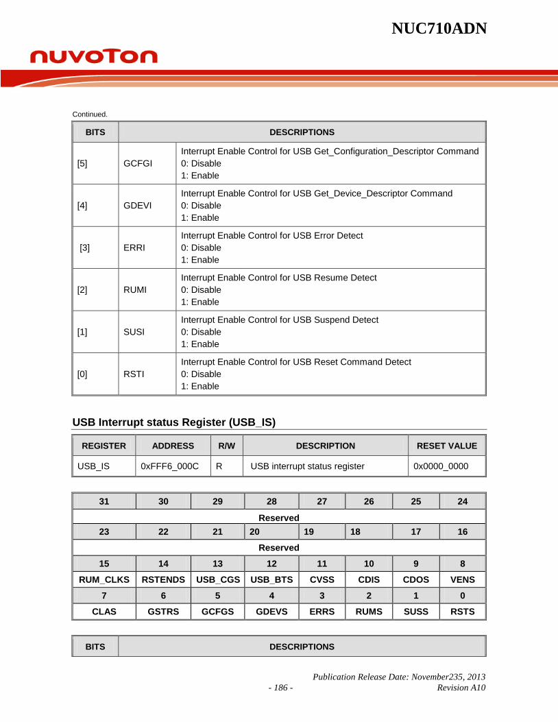
NUC710ADN
Publication Release Date: November235, 2013 - 186 - Revision A10
Continued.
BITS DESCRIPTIONS
[5] GCFGI Interrupt Enable Control for USB Get_Configuration_Descriptor Command 0: Disable 1: Enable
[4] GDEVI Interrupt Enable Control for USB Get_Device_Descriptor Command 0: Disable 1: Enable
[3] ERRI Interrupt Enable Control for USB Error Detect 0: Disable 1: Enable
[2] RUMI Interrupt Enable Control for USB Resume Detect 0: Disable 1: Enable
[1] SUSI Interrupt Enable Control for USB Suspend Detect 0: Disable 1: Enable
[0] RSTI Interrupt Enable Control for USB Reset Command Detect 0: Disable 1: Enable
USB Interrupt status Register (USB_IS)
REGISTER ADDRESS R/W DESCRIPTION RESET VALUE
USB_IS 0xFFF6_000C R USB interrupt status register 0x0000_0000
31 30 29 28 27 26 25 24
Reserved 23 22 21 20 19 18 17 16
Reserved
15 14 13 12 11 10 9 8
RUM_CLKS RSTENDS USB_CGS USB_BTS CVSS CDIS CDOS VENS
7 6 5 4 3 2 1 0
CLAS GSTRS GCFGS GDEVS ERRS RUMS SUSS RSTS
BITS DESCRIPTIONS

NUC710ADN
Publication Release Date: November23, 2013 - 187 - Revision A10
[31:16] Reserved
[15] RUM_CLKS Interrupt status for RESUME (if clock is stopped) 0: No Interrupt Generated 1: Interrupt Generated
[14] RSTENDS Interrupt status for USB reset end 0: No Interrupt Generated 1: Interrupt Generated
[13] USB_CGS Interrupt Status for USB Device Configured 0: No Interrupt Generated 1: Interrupt Generated (configuration changed)
[12] USB_BTS Interrupt Status for USB Bus Transition 0: No Interrupt Generated 1: Interrupt Generated
[11] CVSS Interrupt Status for Status Phase of Class or Vendor Command 0: No Interrupt Generated 1: Interrupt Generated
[10] CDIS Interrupt Status for Data-In of Class or Vendor Command 0: No Interrupt Generated 1: Interrupt Generated
[9] CDOS Interrupt Status for Data-Out of Class or Vendor Command 0: No Interrupt Generated 1: Interrupt Generated
[8] VENS Interrupt Status for USB Vendor Command 0: No Interrupt Generated 1: Interrupt Generated
[7] CLAS Interrupt Status for USB Class Command 0: No Interrupt Generated 1: Interrupt Generated

NUC710ADN
Publication Release Date: November235, 2013 - 188 - Revision A10
Continued.
BITS DESCRIPTIONS
[6] GSTRS Interrupt Status for USB Get_String_Descriptor Command 0: No Interrupt Generated 1: Interrupt Generated
[5] GCFGS Interrupt Status for USB Get_Configuration_Descriptor Command 0: No Interrupt Generated 1: Interrupt Generated
[4] GDEVS Interrupt Status for USB Get_Device_Descriptor Command 0: No Interrupt Generated 1: Interrupt Generated
[3] ERRS Interrupt Status for USB Error Detected 0: No Interrupt Generated 1: Interrupt Generated
[2] RUMS Interrupt Status for USB Resume Detected 0: No Interrupt Generated 1: Interrupt Generated
[1] SUSS Interrupt Status for USB Suspend Detected 0: No Interrupt Generated 1: Interrupt Generated
[0] RSTS Interrupt Status for USB Reset Command Detected 0: No Interrupt Generated 1: Interrupt Generated
USB Interrupt Status Clear (USB_IC)
REGISTER ADDRESS R/W DESCRIPTION RESET VALUE
USB_IC 0xFFF6_0010 R/W USB interrupt status clear register 0x0000_0000
31 30 29 28 27 26 25 24
Reserved 23 22 21 20 19 18 17 16
Reserved 15 14 13 12 11 10 9 8
RUM_CLKC RSTENDC USB_CGC USB_BTC CVSC CDIC CDOC VENC 7 6 5 4 3 2 1 0
CLAC GSTRC GCFGC GDEVC ERRC RUMC SUSC RSTC
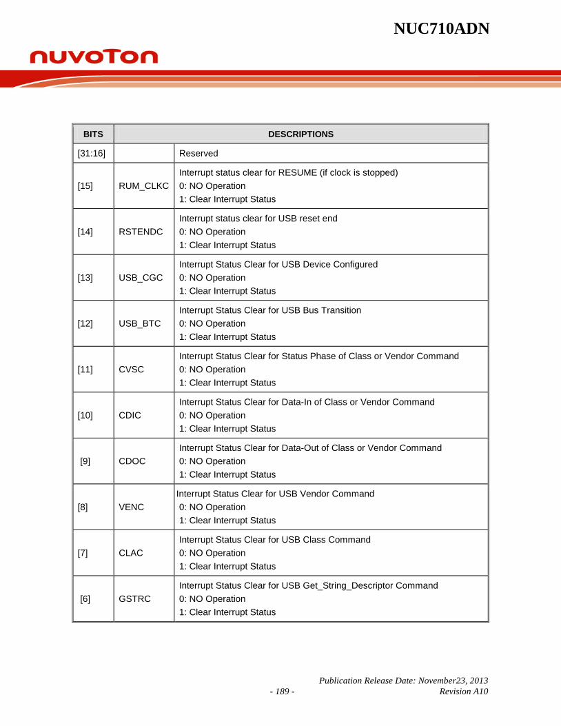
NUC710ADN
Publication Release Date: November23, 2013 - 189 - Revision A10
BITS DESCRIPTIONS
[31:16] Reserved
[15] RUM_CLKC Interrupt status clear for RESUME (if clock is stopped) 0: NO Operation 1: Clear Interrupt Status
[14] RSTENDC Interrupt status clear for USB reset end 0: NO Operation 1: Clear Interrupt Status
[13] USB_CGC Interrupt Status Clear for USB Device Configured 0: NO Operation 1: Clear Interrupt Status
[12] USB_BTC Interrupt Status Clear for USB Bus Transition 0: NO Operation 1: Clear Interrupt Status
[11] CVSC Interrupt Status Clear for Status Phase of Class or Vendor Command 0: NO Operation 1: Clear Interrupt Status
[10] CDIC Interrupt Status Clear for Data-In of Class or Vendor Command 0: NO Operation 1: Clear Interrupt Status
[9] CDOC Interrupt Status Clear for Data-Out of Class or Vendor Command 0: NO Operation 1: Clear Interrupt Status
[8] VENC Interrupt Status Clear for USB Vendor Command
0: NO Operation 1: Clear Interrupt Status
[7] CLAC Interrupt Status Clear for USB Class Command 0: NO Operation 1: Clear Interrupt Status
[6] GSTRC Interrupt Status Clear for USB Get_String_Descriptor Command 0: NO Operation 1: Clear Interrupt Status
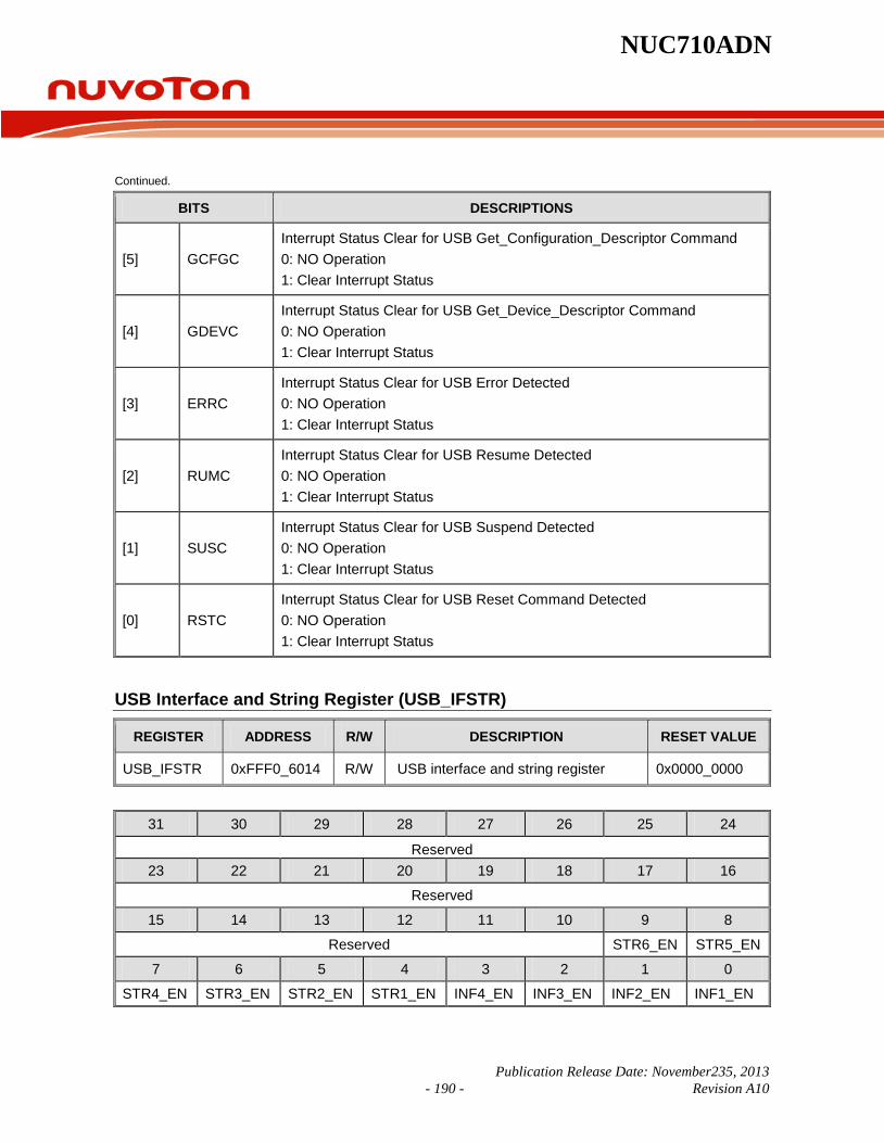
NUC710ADN
Publication Release Date: November235, 2013 - 190 - Revision A10
Continued.
BITS DESCRIPTIONS
[5] GCFGC Interrupt Status Clear for USB Get_Configuration_Descriptor Command 0: NO Operation 1: Clear Interrupt Status
[4] GDEVC Interrupt Status Clear for USB Get_Device_Descriptor Command 0: NO Operation 1: Clear Interrupt Status
[3] ERRC Interrupt Status Clear for USB Error Detected 0: NO Operation 1: Clear Interrupt Status
[2] RUMC Interrupt Status Clear for USB Resume Detected 0: NO Operation 1: Clear Interrupt Status
[1] SUSC Interrupt Status Clear for USB Suspend Detected 0: NO Operation 1: Clear Interrupt Status
[0] RSTC Interrupt Status Clear for USB Reset Command Detected 0: NO Operation 1: Clear Interrupt Status
USB Interface and String Register (USB_IFSTR)
REGISTER ADDRESS R/W DESCRIPTION RESET VALUE
USB_IFSTR 0xFFF0_6014 R/W USB interface and string register 0x0000_0000
31 30 29 28 27 26 25 24
Reserved 23 22 21 20 19 18 17 16
Reserved
15 14 13 12 11 10 9 8
Reserved STR6_EN STR5_EN
7 6 5 4 3 2 1 0
STR4_EN STR3_EN STR2_EN STR1_EN INF4_EN INF3_EN INF2_EN INF1_EN

NUC710ADN
Publication Release Date: November23, 2013 - 191 - Revision A10
BITS DESCRIPTIONS
[31:10] Reserved
[9] STR6_EN USB String Descriptor-6 Control 0: Disable 1: Enable
[8] STR5_EN USB String Descriptor-5 Control 0: Disable 1: Enable
[7] STR4_EN USB String Descriptor-4 Control 0: Disable 1: Enable
[6] STR3_EN USB String Descriptor-3 Control 0: Disable 1: Enable
[5] STR2_EN USB String Descriptor-2 Control 0: Disable 1: Enable
[4] STR1_EN USB String Descriptor-1 Control 0: Disable 1: Enable
[3] INF4_EN USB Interface-4 Control 0: Disable 1: Enable
[2] INF3_EN USB Interface-3 Control 0: Disable 1: Enable
[1] INF2_EN USB Interface-2 Control 0: Disable 1: Enable
[0] INF1_EN USB Interface-1 Control 0: Disable 1: Enable

NUC710ADN
Publication Release Date: November235, 2013 - 192 - Revision A10
USB Control transfer-out port 0 (USB_ODATA0)
REGISTER ADDRESS R/W DESCRIPTION RESET VALUE
USB_ODATA0 0xFFF0_6018 R USB control transfer-out port 0 register 0x0000_0000
31 30 29 28 27 26 25 24
ODATA0 23 22 21 20 19 18 17 16
ODATA0
15 14 13 12 11 10 9 8
ODATA0
7 6 5 4 3 2 1 0
ODATA0
BITS DESCRIPTIONS
[31:0] ODATA0 Control Transfer-out data 0
USB Control transfer-out port 1 (USB_ODATA1)
REGISTER ADDRESS R/W DESCRIPTION RESET VALUE
USB_ODATA1 0xFFF0_601C R USB control transfer-out port 1 register 0x0000_0000
31 30 29 28 27 26 25 24
ODATA1 23 22 21 20 19 18 17 16
ODATA1
15 14 13 12 11 10 9 8
ODATA1
7 6 5 4 3 2 1 0
ODATA1
BITS DESCRIPTIONS
[31:0] ODATA1 Control Transfer-out data 1
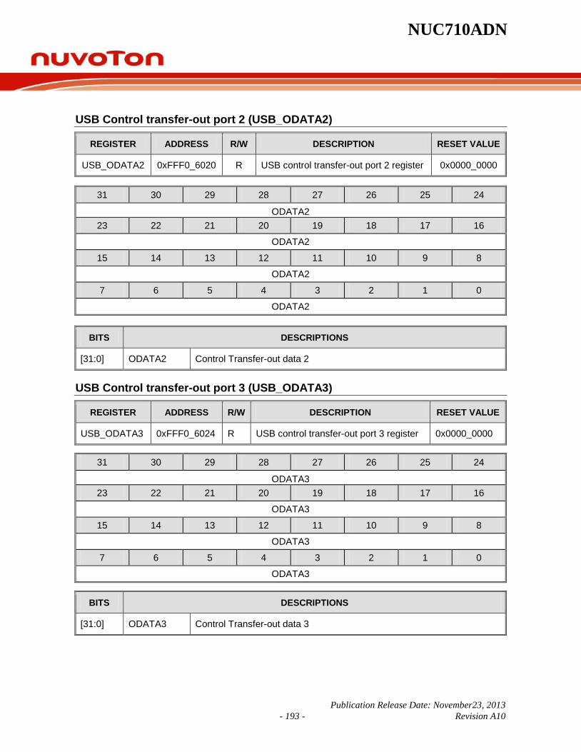
NUC710ADN
Publication Release Date: November23, 2013 - 193 - Revision A10
USB Control transfer-out port 2 (USB_ODATA2)
REGISTER ADDRESS R/W DESCRIPTION RESET VALUE
USB_ODATA2 0xFFF0_6020 R USB control transfer-out port 2 register 0x0000_0000
31 30 29 28 27 26 25 24
ODATA2 23 22 21 20 19 18 17 16
ODATA2
15 14 13 12 11 10 9 8
ODATA2
7 6 5 4 3 2 1 0
ODATA2
BITS DESCRIPTIONS
[31:0] ODATA2 Control Transfer-out data 2
USB Control transfer-out port 3 (USB_ODATA3)
REGISTER ADDRESS R/W DESCRIPTION RESET VALUE
USB_ODATA3 0xFFF0_6024 R USB control transfer-out port 3 register 0x0000_0000
31 30 29 28 27 26 25 24
ODATA3 23 22 21 20 19 18 17 16
ODATA3
15 14 13 12 11 10 9 8
ODATA3
7 6 5 4 3 2 1 0
ODATA3
BITS DESCRIPTIONS
[31:0] ODATA3 Control Transfer-out data 3
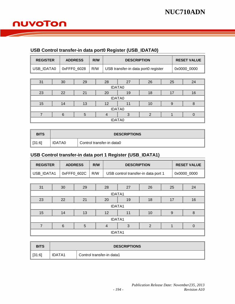
NUC710ADN
Publication Release Date: November235, 2013 - 194 - Revision A10
USB Control transfer-in data port0 Register (USB_IDATA0)
REGISTER ADDRESS R/W DESCRIPTION RESET VALUE
USB_IDATA0 0xFFF0_6028 R/W USB transfer-in data port0 register 0x0000_0000
31 30 29 28 27 26 25 24
IDATA0 23 22 21 20 19 18 17 16
IDATA0 15 14 13 12 11 10 9 8
IDATA0 7 6 5 4 3 2 1 0
IDATA0
BITS DESCRIPTIONS
[31:6] IDATA0 Control transfer-in data0
USB Control transfer-in data port 1 Register (USB_IDATA1)
REGISTER ADDRESS R/W DESCRIPTION RESET VALUE
USB_IDATA1 0xFFF0_602C R/W USB control transfer-in data port 1 0x0000_0000
31 30 29 28 27 26 25 24
IDATA1 23 22 21 20 19 18 17 16
IDATA1
15 14 13 12 11 10 9 8
IDATA1
7 6 5 4 3 2 1 0
IDATA1
BITS DESCRIPTIONS
[31:6] IDATA1 Control transfer-in data1

NUC710ADN
Publication Release Date: November23, 2013 - 195 - Revision A10
USB Control transfer-in data port 2 Register (USB_IDATA2)
REGISTER ADDRESS R/W DESCRIPTION RESET VALUE
USB_IDATA2 0xFFF0_6030 R/W USB control transfer-in data port 2 0x0000_0000
31 30 29 28 27 26 25 24 IDATA2
23 22 21 20 19 18 17 16 IDATA2
15 14 13 12 11 10 9 8 IDATA2
7 6 5 4 3 2 1 0 IDATA2
BITS DESCRIPTIONS
[31:6] IDATA2 Control transfer-in data2
USB Control transfer-in data port 3 Register (USB_IDATA3)
REGISTER ADDRESS R/W DESCRIPTION RESET VALUE
USB_IDATA3 0xFFF0_6034 R/W USB control transfer-in data port 3 0x0000_0000
31 30 29 28 27 26 25 24 IDATA3
23 22 21 20 19 18 17 16 IDATA3
15 14 13 12 11 10 9 8 IDATA3
7 6 5 4 3 2 1 0 IDATA3
BITS DESCRIPTIONS
[31:6] IDATA3 Control transfer-in data3
USB SIE Status Register (USB_SIE)
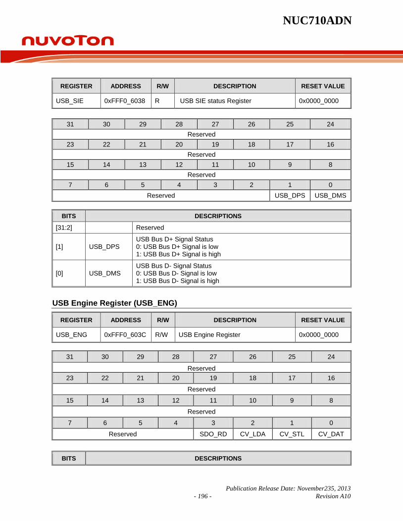
NUC710ADN
Publication Release Date: November235, 2013 - 196 - Revision A10
REGISTER ADDRESS R/W DESCRIPTION RESET VALUE
USB_SIE 0xFFF0_6038 R USB SIE status Register 0x0000_0000
31 30 29 28 27 26 25 24
Reserved 23 22 21 20 19 18 17 16
Reserved 15 14 13 12 11 10 9 8
Reserved 7 6 5 4 3 2 1 0
Reserved USB_DPS USB_DMS
BITS DESCRIPTIONS
[31:2] Reserved
[1] USB_DPS USB Bus D+ Signal Status 0: USB Bus D+ Signal is low 1: USB Bus D+ Signal is high
[0] USB_DMS USB Bus D- Signal Status 0: USB Bus D- Signal is low 1: USB Bus D- Signal is high
USB Engine Register (USB_ENG)
REGISTER ADDRESS R/W DESCRIPTION RESET VALUE
USB_ENG 0xFFF0_603C R/W USB Engine Register 0x0000_0000
31 30 29 28 27 26 25 24
Reserved 23 22 21 20 19 18 17 16
Reserved
15 14 13 12 11 10 9 8
Reserved
7 6 5 4 3 2 1 0
Reserved SDO_RD CV_LDA CV_STL CV_DAT
BITS DESCRIPTIONS

NUC710ADN
Publication Release Date: November23, 2013 - 197 - Revision A10
[31:4] - Reserved
[3] SDO_RD
Setup or Bulk-Out Data Read Control 0: NO Operation 1: Read Setup or Bulk-Out Data from USB Host NOTE: this bit will auto clear after 32 HCLK
[2] CV_LDA
USB Class and Vendor Command Last Data Packet Control 0: NO Operation 1: Last Data Packet for Data Input of Class and Vendor Command NOTE: this bit will auto clear after 32 HCLK
[1] CV_STL
USB Class and Vendor Command Stall Control 0: NO Operation 1: Return Stall for Class and Vendor Command NOTE: this bit will auto clear after 32 HCLK
[0] CV_DAT
USB Class and Vendor Command return data control 0: NO Operation 1: The Data Packet for Data Input of Class and Vendor Command or Get Descriptor command is ready. NOTE: this bit will auto clear after 32 HCLK
USB Control Register (USB_CTLS)
REGISTER ADDRESS R/W DESCRIPTION RESET VALUE
USB_CTLS 0xFFF0_6040 R USB control transfer status register 0x0000_0000
31 30 29 28 27 26 25 24
Reserved 23 22 21 20 19 18 17 16
Reserved
15 14 13 12 11 10 9 8
CONF
7 6 5 4 3 2 1 0
Reserved CTLRPS

NUC710ADN
Publication Release Date: November235, 2013 - 198 - Revision A10
ITS DESCRIPTIONS
[31:16] Reserved
[15:8] CONF USB configured value
[7:5] Reserved
[4:0] CTLRPS Control transfer received packet size
USB Configured Value Register (USB_CONFD)
REGISTER ADDRESS R/W DESCRIPTION RESET VALUE
USB_CONFD 0xFFF0_6044 R/W USB Configured Value register 0x0000_0000
31 30 29 28 27 26 25 24
Reserved 23 22 21 20 19 18 17 16
Reserved 15 14 13 12 11 10 9 8
Reserved 7 6 5 4 3 2 1 0
CONFD
BITS DESCRIPTIONS
[31:8] Reserved
[7:0] CONFD Software configured value
USB Endpoint A Information Register (EPA_INFO)
REGISTER ADDRESS R/W DESCRIPTION RESET VALUE
EPA_INFO 0xFFF0_6048 R/W USB endpoint A information register 0x0000_0000
31 30 29 28 27 26 25 24
Reserved EPA_TYPE EPA_DIR Reserved EPA_MPS 23 22 21 20 19 18 17 16
EPA_MPS 15 14 13 12 11 10 9 8
EPA_ALT EPA_INF 7 6 5 4 3 2 1 0
EPA_CFG EPA_NUM
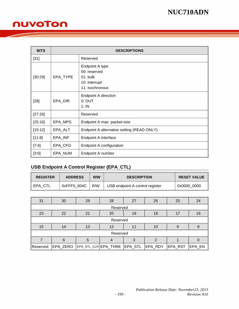
NUC710ADN
Publication Release Date: November23, 2013 - 199 - Revision A10
BITS DESCRIPTIONS
[31] Reserved
[30:29] EPA_TYPE
Endpoint A type 00: reserved 01: bulk 10: interrupt 11: isochronous
[28] EPA_DIR Endpoint A direction 0: OUT 1: IN
[27:26] Reserved
[25:16] EPA_MPS Endpoint A max. packet-size
[15:12] EPA_ALT Endpoint A alternative setting (READ ONLY)
[11:8] EPA_INF Endpoint A interface
[7:4] EPA_CFG Endpoint A configuration
[3:0] EPA_NUM Endpoint A number
USB Endpoint A Control Register (EPA_CTL)
REGISTER ADDRESS R/W DESCRIPTION RESET VALUE
EPA_CTL 0xFFF0_604C R/W USB endpoint A control register 0x0000_0000
31 30 29 28 27 26 25 24
Reserved 23 22 21 20 19 18 17 16
Reserved
15 14 13 12 11 10 9 8
Reserved
7 6 5 4 3 2 1 0
Reserved EPA_ZERO EPA_STL_CLR EPA_THRE EPA_STL EPA_RDY EPA_RST EPA_EN
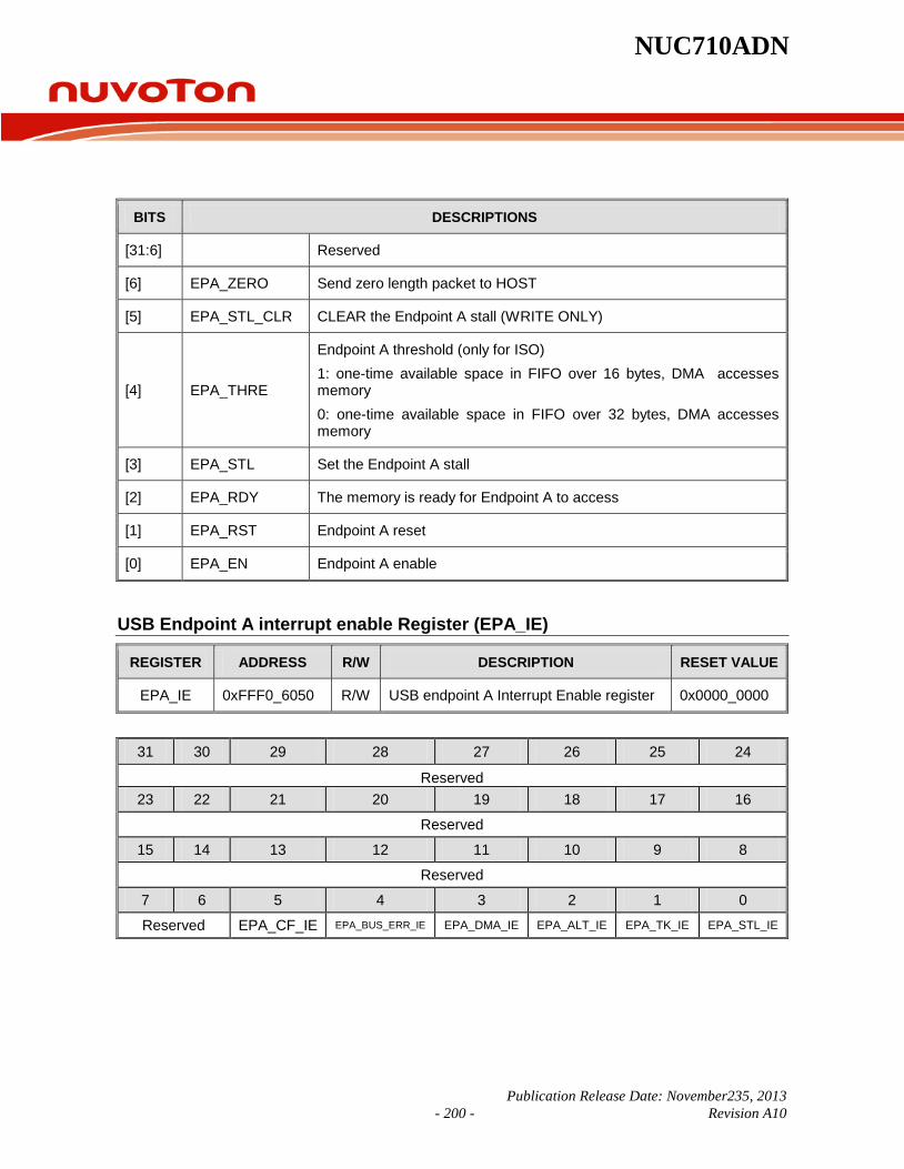
NUC710ADN
Publication Release Date: November235, 2013 - 200 - Revision A10
BITS DESCRIPTIONS
[31:6] Reserved
[6] EPA_ZERO Send zero length packet to HOST
[5] EPA_STL_CLR CLEAR the Endpoint A stall (WRITE ONLY)
[4] EPA_THRE
Endpoint A threshold (only for ISO) 1: one-time available space in FIFO over 16 bytes, DMA accesses memory 0: one-time available space in FIFO over 32 bytes, DMA accesses memory
[3] EPA_STL Set the Endpoint A stall
[2] EPA_RDY The memory is ready for Endpoint A to access
[1] EPA_RST Endpoint A reset
[0] EPA_EN Endpoint A enable
USB Endpoint A interrupt enable Register (EPA_IE)
REGISTER ADDRESS R/W DESCRIPTION RESET VALUE
EPA_IE 0xFFF0_6050 R/W USB endpoint A Interrupt Enable register 0x0000_0000
31 30 29 28 27 26 25 24
Reserved 23 22 21 20 19 18 17 16
Reserved
15 14 13 12 11 10 9 8
Reserved
7 6 5 4 3 2 1 0
Reserved EPA_CF_IE EPA_BUS_ERR_IE EPA_DMA_IE EPA_ALT_IE EPA_TK_IE EPA_STL_IE

NUC710ADN
Publication Release Date: November23, 2013 - 201 - Revision A10
BITS DESCRIPTIONS
[31:6] Reserved
[5] EPA_CF_IE Endpoint A clear feature interrupt enable
[4] EPA_BUS_ERR_IE Endpoint A system bus error interrupt enable
[3] EPA_DMA_IE Endpoint A DMA transfer complete interrupt enable
[2] EPA_ALT_IE Endpoint A alternate setting interrupt enable
[1] EPA_TK_IE Endpoint A token input interrupt enable
[0] EPA_STL_IE Endpoint A stall interrupt enable
USB Endpoint A Interrupt Clear Register (EPA_IC)
REGISTER ADDRESS R/W DESCRIPTION RESET VALUE
EPA_IC 0xFFF0_6054 W USB endpoint A interrupt clear register 0x0000_0000
31 30 29 28 27 26 25 24 Reserved
23 22 21 20 19 18 17 16 Reserved
15 14 13 12 11 10 9 8 Reserved
7 6 5 4 3 2 1 0 Reserved EPA_CF_IC EPA_BUS_ERR_IC EPA_DMA_IC EPA_ALT_IC EPA_TK_IC EPA_STL_IC
BITS DESCRIPTIONS
[31:6] Reserved
[5] EPA_CF_INT_IC Endpoint A clear feature interrupt clear
[4] EPA_BUS_ERR_IC Endpoint A system bus error interrupt clear
[3] EPA_DMA_IC Endpoint A DMA transfer complete interrupt clear
[2] EPA_ALT_IC Endpoint A alternate setting interrupt clear
[1] EPA_TK_IC Endpoint A token input interrupt clear
[0] EPA_STL_IC Endpoint A stall interrupt clear
USB Endpoint A Interrupt Status Register (EPA_IS)
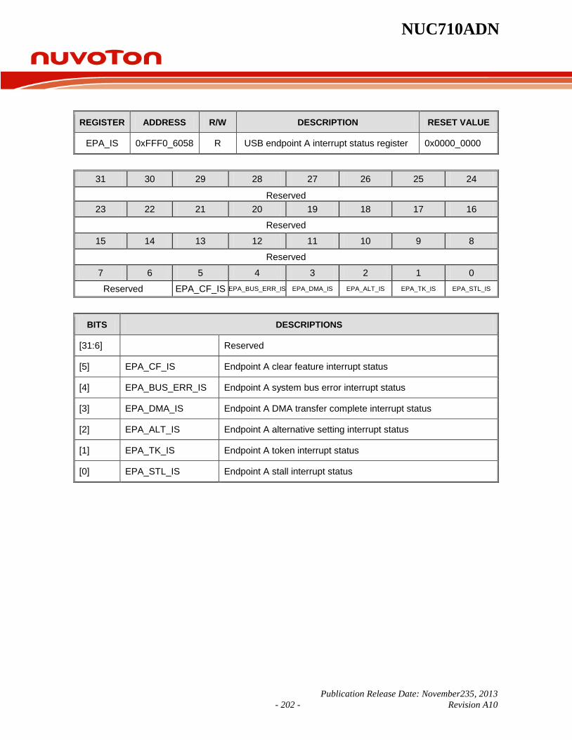
NUC710ADN
Publication Release Date: November235, 2013 - 202 - Revision A10
REGISTER ADDRESS R/W DESCRIPTION RESET VALUE
EPA_IS 0xFFF0_6058 R USB endpoint A interrupt status register 0x0000_0000
31 30 29 28 27 26 25 24
Reserved 23 22 21 20 19 18 17 16
Reserved
15 14 13 12 11 10 9 8
Reserved
7 6 5 4 3 2 1 0
Reserved EPA_CF_IS EPA_BUS_ERR_IS EPA_DMA_IS EPA_ALT_IS EPA_TK_IS EPA_STL_IS
BITS DESCRIPTIONS
[31:6] Reserved
[5] EPA_CF_IS Endpoint A clear feature interrupt status
[4] EPA_BUS_ERR_IS Endpoint A system bus error interrupt status
[3] EPA_DMA_IS Endpoint A DMA transfer complete interrupt status
[2] EPA_ALT_IS Endpoint A alternative setting interrupt status
[1] EPA_TK_IS Endpoint A token interrupt status
[0] EPA_STL_IS Endpoint A stall interrupt status
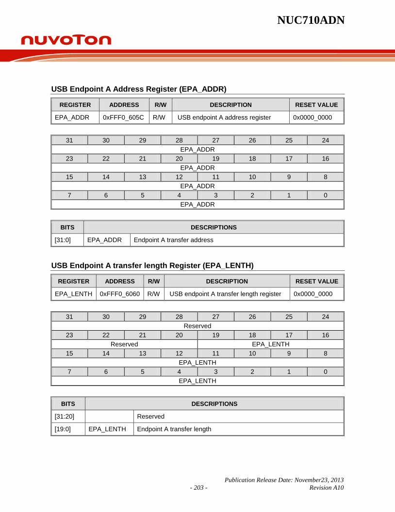
NUC710ADN
Publication Release Date: November23, 2013 - 203 - Revision A10
USB Endpoint A Address Register (EPA_ADDR)
REGISTER ADDRESS R/W DESCRIPTION RESET VALUE
EPA_ADDR 0xFFF0_605C R/W USB endpoint A address register 0x0000_0000
31 30 29 28 27 26 25 24
EPA_ADDR 23 22 21 20 19 18 17 16
EPA_ADDR 15 14 13 12 11 10 9 8
EPA_ADDR 7 6 5 4 3 2 1 0
EPA_ADDR
BITS DESCRIPTIONS
[31:0] EPA_ADDR Endpoint A transfer address
USB Endpoint A transfer length Register (EPA_LENTH)
REGISTER ADDRESS R/W DESCRIPTION RESET VALUE
EPA_LENTH 0xFFF0_6060 R/W USB endpoint A transfer length register 0x0000_0000
31 30 29 28 27 26 25 24
Reserved 23 22 21 20 19 18 17 16
Reserved EPA_LENTH 15 14 13 12 11 10 9 8
EPA_LENTH 7 6 5 4 3 2 1 0
EPA_LENTH
BITS DESCRIPTIONS
[31:20] Reserved
[19:0] EPA_LENTH Endpoint A transfer length

NUC710ADN
Publication Release Date: November235, 2013 - 204 - Revision A10
USB Endpoint B Information Register (EPB_INFO)
REGISTER ADDRESS R/W DESCRIPTION RESET VALUE
EPB_INFO 0xFFF0_6064 R/W USB endpoint B information register 0x0000_0000
31 30 29 28 27 26 25 24
Reserved EPB_TYPE EPB_DIR Reserved EPB_MPS 23 22 21 20 19 18 17 16
EPB_MPS
15 14 13 12 11 10 9 8
EPB_ALT EPB_INF
7 6 5 4 3 2 1 0
EPB_CFG EPB_NUM
BITS DESCRIPTIONS
[31] - Reserved
[30:29] EPB_TYPE
Endpoint B type 00: reserved 01: bulk 10: interrupt 11: isochronous
[28] EPB_DIR Endpoint B direction 0: OUT 1: IN
[27:26] - Reserved
[25:16] EPB_MPS Endpoint B max. packet-size
[15:12] EPB_ALT Endpoint B alternative setting (READ ONLY)
[11:8] EPB_INF Endpoint B interface
[7:4] EPB_CFG Endpoint B configuration
[3:0] EPB_NUM Endpoint B number

NUC710ADN
Publication Release Date: November23, 2013 - 205 - Revision A10
USB Endpoint B Control Register (EPB_CTL)
REGISTER ADDRESS R/W DESCRIPTION RESET VALUE
EPB_CTL 0xFFF0_6068 R/W USB endpoint B control register 0x0000_0000
31 30 29 28 27 26 25 24
Reserved 23 22 21 20 19 18 17 16
Reserved
15 14 13 12 11 10 9 8
Reserved
7 6 5 4 3 2 1 0 Reserved EPB_ZERO EPB_STL_CLR EPB_THRE EPB_STL EPB_RDY EPB_RST EPB_EN
BITS DESCRIPTIONS
[31:7] - Reserved
[6] EPB_ZERO Send zero length packet back to HOST
[5] EPB_STL_CLR Clear the Endpoint B stall (WRITE ONLY)
[4] EPB_THRE
Endpoint B threshold (only for ISO) 1: one-time available space in FIFO over 16 bytes, DMA accesses memory 0: one-time available space in FIFO over 32 bytes, DMA accesses memory
[3] EPB_STL Set the Endpoint B stall
[2] EPB_RDY The memory is ready for Endpoint B to access
[1] EPB_RST Endpoint B reset
[0] EPB_EN Endpoint B enable
USB Endpoint B interrupt enable Register (EPB_IE)
REGISTER ADDRESS R/W DESCRIPTION RESET VALUE
EPB_IE 0xFFF0_606C R/W USB endpoint B Interrupt Enable register 0x0000_0000

NUC710ADN
Publication Release Date: November235, 2013 - 206 - Revision A10
31 30 29 28 27 26 25 24
Reserved 23 22 21 20 19 18 17 16
Reserved
15 14 13 12 11 10 9 8
Reserved
7 6 5 4 3 2 1 0
Reserved EPB_CF_IE EPB_BUS_ERR_IE EPB_DMA_IE EPB_ALT_IE EPB_TK_IE EPB_STL_IE
BITS DESCRIPTIONS
[31:6] Reserved
[5] EPB_CF_IE Endpoint B clear feature interrupt enable
[4] EPB_BUS_ERR_IE Endpoint B system bus error interrupt enable
[3] EPB_DMA_IE Endpoint B DMA transfer complete interrupt enable
[2] EPB_ALT_IE Endpoint B alternate setting interrupt enable
[1] EPB_TK_IE Endpoint B token input interrupt enable
[0] EPB_STL_IE Endpoint B stall interrupt enable
USB Endpoint B Interrupt Clear Register (EPB_IC)
REGISTER ADDRESS R/W DESCRIPTION RESET VALUE
EPB_IC 0xFFF0_6070 W USB endpoint B interrupt clear register 0x0000_0000
31 30 29 28 27 26 25 24
Reserved 23 22 21 20 19 18 17 16
Reserved
15 14 13 12 11 10 9 8
Reserved
7 6 5 4 3 2 1 0
Reserved EPB_CF_IC EPB_BUS_ERR_IC EPB_DMA_IC EPB_ALT_IC EPB_TK_IC EPB_STL_IC

NUC710ADN
Publication Release Date: November23, 2013 - 207 - Revision A10
BITS DESCRIPTIONS
[31:6] - Reserved
[5] EPB_CF_IC Endpoint B clear feature interrupt clear
[4] EPB_BUS_ERR_IC Endpoint B system bus error interrupt clear
[3] EPB_DMA_IC Endpoint B DMA transfer complete interrupt clear
[2] EPB_ALT_IC Endpoint B alternate setting interrupt clear
[1] EPB_TK_IC Endpoint B token input interrupt clear
[0] EPB_STL_IC Endpoint B stall interrupt clear
USB Endpoint B Interrupt Status Register (EPB_IS)
REGISTER ADDRESS R/W DESCRIPTION RESET VALUE
EPB_IS 0xFFF0_6074 R USB endpoint B interrupt status register 0x0000_0000
31 30 29 28 27 26 25 24
Reserved 23 22 21 20 19 18 17 16
Reserved
15 14 13 12 11 10 9 8
Reserved
7 6 5 4 3 2 1 0
Reserved EPB_CF_IS EPB_BUS_ERR_IS EPB_DMA_IS EPB_ALT_IS EPB_TK_IS EPB_STL_IS
BITS DESCRIPTIONS
[31:6] - Reserved
[5] EPB_CF_IS Endpoint B clear feature interrupt status
[4] EPB_DMA_IS Endpoint B system bus error interrupt status
[3] EPB_DMA_IS Endpoint B DMA transfer complete interrupt status
[2] EPB_ALT_IS Endpoint B alternative setting interrupt status
[1] EPB_TK_IS Endpoint B token interrupt status
[0] EPB_STL_IS Endpoint B stall interrupt status
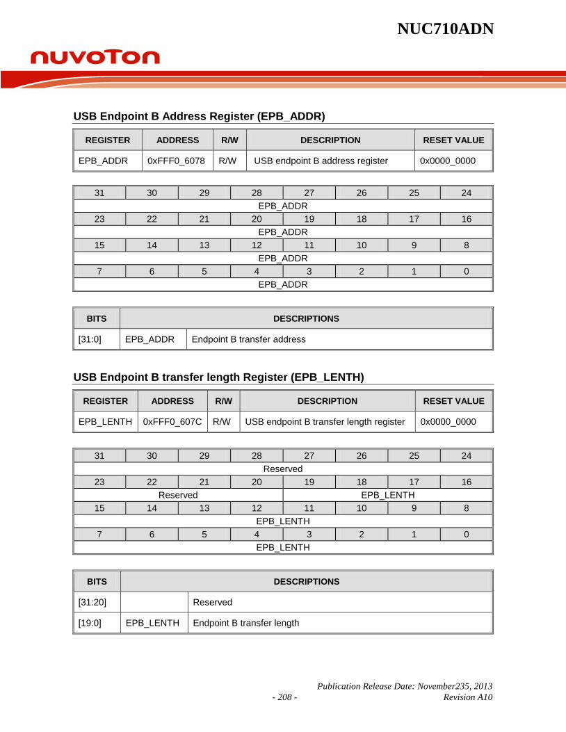
NUC710ADN
Publication Release Date: November235, 2013 - 208 - Revision A10
USB Endpoint B Address Register (EPB_ADDR)
REGISTER ADDRESS R/W DESCRIPTION RESET VALUE
EPB_ADDR 0xFFF0_6078 R/W USB endpoint B address register 0x0000_0000
31 30 29 28 27 26 25 24 EPB_ADDR
23 22 21 20 19 18 17 16 EPB_ADDR
15 14 13 12 11 10 9 8 EPB_ADDR
7 6 5 4 3 2 1 0 EPB_ADDR
BITS DESCRIPTIONS
[31:0] EPB_ADDR Endpoint B transfer address
USB Endpoint B transfer length Register (EPB_LENTH)
REGISTER ADDRESS R/W DESCRIPTION RESET VALUE
EPB_LENTH 0xFFF0_607C R/W USB endpoint B transfer length register 0x0000_0000
31 30 29 28 27 26 25 24
Reserved 23 22 21 20 19 18 17 16
Reserved EPB_LENTH 15 14 13 12 11 10 9 8
EPB_LENTH 7 6 5 4 3 2 1 0
EPB_LENTH
BITS DESCRIPTIONS
[31:20] Reserved
[19:0] EPB_LENTH Endpoint B transfer length

NUC710ADN
Publication Release Date: November23, 2013 - 209 - Revision A10
USB Endpoint C Information Register (EPC_INFO)
REGISTER ADDRESS R/W DESCRIPTION RESET VALUE
EPC_INFO 0xFFF0_6080 R/W USB endpoint C information register 0x0000_0000
31 30 29 28 27 26 25 24
Reserved EPC_TYPE EPC_DIR Reserved EPC_MPS 23 22 21 20 19 18 17 16
EPC_MPS
15 14 13 12 11 10 9 8
EPC_ALT EPC_INF
7 6 5 4 3 2 1 0
EPC_CFG EPC_NUM
BITS DESCRIPTIONS
[31] Reserved
[30:29] EPC_TYPE
Endpoint C type 00: Reserved 01: Bulk 10: Interrupt 11: Isochronous
[28] EPC_DIR Endpoint C direction 0: OUT 1: IN
[27:26] Reserved
[25:16] EPC_MPS Endpoint C max. packet-size
[15:12] EPC_ALT Endpoint C alternative setting (READ ONLY)
[11:8] EPC_INF Endpoint C interface
[7:4] EPC_CFG Endpoint C configuration
[3:0] EPC_NUM Endpoint C number
USB Endpoint C Control Register (EPC_CTL)
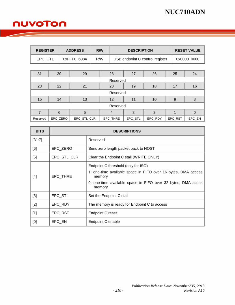
NUC710ADN
Publication Release Date: November235, 2013 - 210 - Revision A10
REGISTER ADDRESS R/W DESCRIPTION RESET VALUE
EPC_CTL 0xFFF0_6084 R/W USB endpoint C control register 0x0000_0000
31 30 29 28 27 26 25 24
Reserved 23 22 21 20 19 18 17 16
Reserved
15 14 13 12 11 10 9 8
Reserved
7 6 5 4 3 2 1 0 Reserved EPC_ZERO EPC_STL_CLR EPC_THRE EPC_STL EPC_RDY EPC_RST EPC_EN
BITS DESCRIPTIONS
[31:7] Reserved
[6] EPC_ZERO Send zero length packet back to HOST
[5] EPC_STL_CLR Clear the Endpoint C stall (WRITE ONLY)
[4] EPC_THRE
Endpoint C threshold (only for ISO) 1: one-time available space in FIFO over 16 bytes, DMA access
memory 0: one-time available space in FIFO over 32 bytes, DMA acces
memory
[3] EPC_STL Set the Endpoint C stall
[2] EPC_RDY The memory is ready for Endpoint C to access
[1] EPC_RST Endpoint C reset
[0] EPC_EN Endpoint C enable
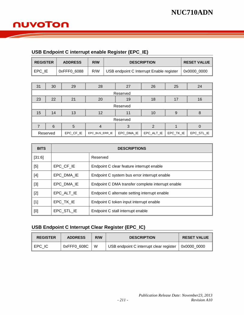
NUC710ADN
Publication Release Date: November23, 2013 - 211 - Revision A10
USB Endpoint C interrupt enable Register (EPC_IE)
REGISTER ADDRESS R/W DESCRIPTION RESET VALUE
EPC_IE 0xFFF0_6088 R/W USB endpoint C Interrupt Enable register 0x0000_0000
31 30 29 28 27 26 25 24
Reserved 23 22 21 20 19 18 17 16
Reserved
15 14 13 12 11 10 9 8
Reserved
7 6 5 4 3 2 1 0
Reserved EPC_CF_IE EPC_BUS_ERR_IE EPC_DMA_IE EPC_ALT_IE EPC_TK_IE EPC_STL_IE
BITS DESCRIPTIONS
[31:6] Reserved
[5] EPC_CF_IE Endpoint C clear feature interrupt enable
[4] EPC_DMA_IE Endpoint C system bus error interrupt enable
[3] EPC_DMA_IE Endpoint C DMA transfer complete interrupt enable
[2] EPC_ALT_IE Endpoint C alternate setting interrupt enable
[1] EPC_TK_IE Endpoint C token input interrupt enable
[0] EPC_STL_IE Endpoint C stall interrupt enable
USB Endpoint C Interrupt Clear Register (EPC_IC)
REGISTER ADDRESS R/W DESCRIPTION RESET VALUE
EPC_IC 0xFFF0_608C W USB endpoint C interrupt clear register 0x0000_0000

NUC710ADN
Publication Release Date: November235, 2013 - 212 - Revision A10
31 30 29 28 27 26 25 24
Reserved 23 22 21 20 19 18 17 16
Reserved
15 14 13 12 11 10 9 8
Reserved
7 6 5 4 3 2 1 0
Reserved EPC_CF_IC EPC_BUS_ERR_IC EPC_DMA_IC EPC_ALT_IC EPC_TK_IC EPC_STL_IC
BITS DESCRIPTIONS
[31:6] Reserved
[5] EPC_CF_IC Endpoint C clear feature interrupt clear
[4] EPC_DMA_IC Endpoint C system bus error interrupt clear
[3] EPC_DMA_IC Endpoint C DMA transfer complete interrupt clear
[2] EPC_ALT_IC Endpoint C alternate setting interrupt clear
[1] EPC_TK_IC Endpoint C token input interrupt clear
[0] EPC_STL_IC Endpoint C stall interrupt clear
USB Endpoint C Interrupt Status Register (EPC_IS)
REGISTER ADDRESS R/W DESCRIPTION RESET VALUE
EPC_IS 0xFFF0_6090 R USB endpoint C interrupt status register 0x0000_0000
31 30 29 28 27 26 25 24
Reserved 23 22 21 20 19 18 17 16
Reserved
15 14 13 12 11 10 9 8
Reserved
7 6 5 4 3 2 1 0
Reserved EPC_CF_IS EPC_BUS_ERR_IS EPC_DMA_IS EPC_ALT_IS EPC_TK_IS EPC_STL_IS

NUC710ADN
Publication Release Date: November23, 2013 - 213 - Revision A10
BITS DESCRIPTIONS
[31:6] Reserved
[5] EPC_CF_IS Endpoint C clear feature interrupt status
[4] EPC_BUS_ERR_IS Endpoint A system bus error interrupt status
[3] EPC_DMA_IS Endpoint A DMA transfer complete interrupt status
[2] EPC_ALT_IS Endpoint A alternative setting interrupt status
[1] EPC_TK_IS Endpoint A token interrupt status
[0] EPC_STL_IS Endpoint A stall status
USB Endpoint C Address Register (EPC_ADDR)
REGISTER ADDRESS R/W DESCRIPTION RESET VALUE
EPC_ADDR 0xFFF0_6094 R/W USB endpoint C address register 0x0000_0000
31 30 29 28 27 26 25 24
EPC_ADDR 23 22 21 20 19 18 17 16
EPC_ADDR
15 14 13 12 11 10 9 8
EPC_ADDR
7 6 5 4 3 2 1 0
EPC_ADDR
BITS DESCRIPTIONS
[31:0] EPC_ADDR Endpoint C transfer address
USB Endpoint C transfer length Register (EPC_LENTH)
REGISTER ADDRESS R/W DESCRIPTION RESET VALUE
EPC_LENTH 0xFFF0_6098 R/W USB endpoint C transfer length register 0x0000_0000
31 30 29 28 27 26 25 24
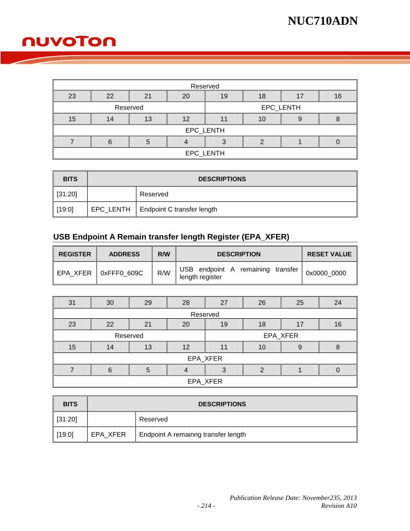
NUC710ADN
Publication Release Date: November235, 2013 - 214 - Revision A10
Reserved 23 22 21 20 19 18 17 16
Reserved EPC_LENTH
15 14 13 12 11 10 9 8
EPC_LENTH
7 6 5 4 3 2 1 0
EPC_LENTH
BITS DESCRIPTIONS
[31:20] Reserved
[19:0] EPC_LENTH Endpoint C transfer length
USB Endpoint A Remain transfer length Register (EPA_XFER)
REGISTER ADDRESS R/W DESCRIPTION RESET VALUE
EPA_XFER 0xFFF0_609C R/W USB endpoint A remaining transfer length register 0x0000_0000
31 30 29 28 27 26 25 24
Reserved 23 22 21 20 19 18 17 16
Reserved EPA_XFER
15 14 13 12 11 10 9 8
EPA_XFER
7 6 5 4 3 2 1 0
EPA_XFER
BITS DESCRIPTIONS
[31:20] Reserved
[19:0] EPA_XFER Endpoint A remainng transfer length

NUC710ADN
Publication Release Date: November23, 2013 - 215 - Revision A10
USB Endpoint A Remain packet length Register (EPA_PKT)
REGISTER ADDRESS R/W DESCRIPTION RESET VALUE
EPA_PKT 0xFFF0_60A0 R/W USB endpoint A remain packet length register 0x0000_0000
31 30 29 28 27 26 25 24
Reserved 23 22 21 20 19 18 17 16
Reserved 15 14 13 12 11 10 9 8
Reserved EPA_PKT 7 6 5 4 3 2 1 0
EPA_PKT
BITS Descriptions
[31:10] Reserved
[9:0] EPA_PKT Endpoint A remain packet length
USB Endpoint B Remain transfer length Register (EPB_XFER)
REGISTER ADDRESS R/W DESCRIPTION RESET VALUE
EPB_XFER 0xFFF0_60A4 R/W USB endpoint B remain transfer length register 0x0000_0000
31 30 29 28 27 26 25 24 Reserved
23 22 21 20 19 18 17 16 Reserved EPB_XFER
15 14 13 12 11 10 9 8 EPB_XFER
7 6 5 4 3 2 1 0 EPB_XFER
BITS DESCRIPTIONS
[31:20] Reserved
[19:0] EPB_XFER Endpoint B remain transfer length
USB Endpoint B Remain packet length Register (EPB_PKT)

NUC710ADN
Publication Release Date: November235, 2013 - 216 - Revision A10
REGISTER ADDRESS R/W DESCRIPTION RESET VALUE
EPB_PKT 0xFFF0_60A8 R/W USB endpoint B remain packet length register 0x0000_0000
31 30 29 28 27 26 25 24
Reserved 23 22 21 20 19 18 17 16
Reserved
15 14 13 12 11 10 9 8
Reserved EPB_PKT
7 6 5 4 3 2 1 0
EPB_PKT
BITS DESCRIPTIONS
[31:10] Reserved
[9:0] EPB_PKT Endpoint B remaining packet length
USB Endpoint C Remain transfer length Register (EPC_XFER)
REGISTER ADDRESS R/W DESCRIPTION RESET VALUE
EPC_XFER 0xFFF0_60AC R/W USB endpoint C remaining transfer length register 0x0000_0000
31 30 29 28 27 26 25 24
Reserved 23 22 21 20 19 18 17 16
Reserved EPC_XFER
15 14 13 12 11 10 9 8
EPC_XFER
7 6 5 4 3 2 1 0
EPC_XFER
BITS DESCRIPTIONS

NUC710ADN
Publication Release Date: November23, 2013 - 217 - Revision A10
[31:20] Reserved
[19:0] EPC_XFER Endpoint C remaining transfer length
USB Endpoint C Remain packet length Register (EPC_PKT)
REGISTER ADDRESS R/W DESCRIPTION RESET VALUE
EPC_PKT 0xFFF0_60B0 R/W USB endpoint C remaining packet length register 0x0000_0000
31 30 29 28 27 26 25 24
Reserved 23 22 21 20 19 18 17 16
Reserved
15 14 13 12 11 10 9 8
Reserved EPC_PKT
7 6 5 4 3 2 1 0
EPC_PKT
BITS DESCRIPTIONS
[31:10] Reserved
[9:0] EPC_PKT Endpoint C remaining packet length

NUC710ADN
Publication Release Date: November235, 2013 - 218 - Revision A10
6.9 SD Host Controller The NUC710 SD host controller supports Secure Digital (SD, MMC) card devices. The SD host-controller also supports DMA functions to reduce the intervention of the CPU for data transfers between flash memory cards and system memory.
There are two 512B internal buffers embedded in the SD host controller to temporally buffer the data for DMA transfer between the flash memory card and system memory.
The SD host controller features are shown as below:
Directly connect to Secure Digital (SD, MMC) flash memory card. Supports DMA function to accelerate the data transfer between the internal buffer, external
SDRAM, and flash memory card. Two 512 bytes internal buffers are embedded inside of the SD host controller. No SPI mode.
6.9.1 Functional Description
SD host controller provides three signals, CLK, CMD and DAT[3:0], to all SD cards. CLK is a clock output signal. CMD and DAT[3:0] are bi-direction command and data signals, respectively.
The frequency of CLK is equal to (engine clock frequency)/(SD_CLK+1), where SD_CLK is the value of the SD clock control register. To save power, CLK is active only when there are activities between SD host controller and SD cards. Otherwise, CLK keeps inactive state (LOW).
According to the SD specification, the SD host controller provides several operations to communicate with SD Cards efficiently. The CPU writes to the SD access control register to setup operations.
When the command output enable bit of the SD access control register is set, SD host controller transfers a 48-bit command to one or more SD card. When the transfer is done, this bit is reset to 0 automatically.
For a 48-bits command, the 6-bits command number is coming from SD CMD code register and the 32-bits command argument is coming from SD command argument 1-4 registers. All other bits (including start bit, end bit and the CRC-7bits) are generated by SD host controller H/W circuit.
When the response input enable bit of the SD access control register is set, the SD host controller waits for a 48-bit response from one or more SD card. When a 48-bit response is received, this bit is automatically reset to 0.
The first 40 bits of the received response are stored into SD received response token1 – 5 registers.
The last 8 bits are CRC-7 bits and end bit. SD host controller H/W circuit checks CRC-7 and reports the result to SD status register.
When the data input enable bit of SD access control register is set, SD host controller waits for a block of data from a specific SD card. When a block of data is received, this bit is cleared to 0 automatically.
The received block of data is stored into the system memory and the address is starting from the address specified by S/W.
NUC710ADN
Publication Release Date: November23, 2013 - 219 - Revision A10
SD host controller checks the associated CRC-16 bits and reports the result to SD status register.
If the data-input interrupt is enabled, an interrupt occurs when data transfer is finished. The data input status bit of SD status register is set as 1 for this interrupt. Thus, the CPU can identify a data-input interrupt by reading this bit.
When the data output enable bit of SD access control register is set, SD host controller transfers a block of data to a specific MMC card. When the data transfer is finished, this bit is cleared to 0 automatically.
Before the data is transferred, the data to be transmitted must be stored into system memory and the S/W must specified the starting address where the data is stored.
SD host controller will generate the associated CRC-16 bits itself. After the data is transmitted, it also checks the CRC-status response from the SD card. The result is stored into the SD status register.
If the data-output interrupt is enabled, an interrupt will occur when the data transfer is finished. The data output status bit of the SD status register is set to 1 for this interrupt. Thus, the CPU can identify a data-output interrupt by reading this bit.
1. When the response R2 input enable bit of SD access control register is set, SD host controller transfers a block of data to a specific SD card. When the data transfer is finished and this bit is set, the SD host controller waits for a 136-bit R2 response from the SD card. When the R2 response is completely received, the bit is reset to 0 automatically.
The received data of R2 response token (136-bit) is stored into the system memory, starting from the address specified by software.
SD host controller checks the CRC-7 and reports the result to SD status register. 2. When the 74-clock cycles output enable bit of SD access control register is set, SD host controller
generates 74 clock cycles without any CMD or DAT activity. After the 74 clock cycles have been generated, the bit is reset to 0 automatically.

NUC710ADN
Publication Release Date: November235, 2013 - 220 - Revision A10
6.9.2 Register Mapping
REGISTER ADDRESS R/W DESCRIPTION RESET VALUE
SD Registers (6) SDGCR 0xFFF0_0000 R/W SD Global Control Register 0x0000_0000
SDDSA 0xFFF0_0004 R/W SD DMA Transfer Starting Address Register 0x0000_0000
SDBCR 0xFFF0_7008 R/W SD DMA Byte Count Register 0x0000_0000
SDGIER 0xFFF0_700C R/W SD Global Interrupt Enable Register 0x0000_0000
SDGISR 0xFFF0_7010 R/W SD Global Interrupt Status Register 0x0000_0000
SDBIST 0xFFF0_7014 R/W SD BIST Register 0x0000_0000
Secure Digital Registers (8) SDICR 0xFFF0_7300 R/W SD Interface Control Register 0x0000_0000
SDHIIR 0xFFF0_7304 R/W SD Host Interface Initial Register 0x0000_0018
SDIIER 0xFFF0_7308 R/W SD Interface Interrupt Enable Register 0x0000_0000
SDIISR 0xFFF0_730C R/W SD Interface Interrupt Status Register 0x0000_00XX
SDAUG 0xFFF0_7310 R/W SD Command Argument Register 0x0000_0000
SDRSP0 0xFFF0_7314 R SD Receive Response Token Register 0 0xXXXX_XXXX
SDRSP1 0xFFF0_7318 R SD Receive Response Token Register 1 0x0000_XXXX
SDBLEN 0xFFF0_731C R/W SD Block Length Register 0x0000_0000
Internal Buffer Access Register (256) FB0_0 ….. FB0_127
0xFFF0_7400 …..
0xFFF0_75FC R/W Flash Buffer 0 Undefined
FB1_0 ….. FB1_127
0xFFF0_7800 …..
0xFFF0_79FC R/W Flash Buffer 1 Undefined

NUC710ADN
Publication Release Date: November23, 2013 - 221 - Revision A10
6.9.3 SD Register Description
SD Gloal Control Register (SDGCR)
REGISTER ADDRESS R/W DESCRIPTION RESET VALUE
SDGCR 0xFFF0_7000 R/W SD Global Control Register 0x0000_0000
31 30 29 28 27 26 25 24
Reserved
23 22 21 20 19 18 17 16
Reserved
15 14 13 12 11 10 9 8
Reserved RdSel
7 6 5 4 3 2 1 0 Reserved WrSel DMARd DMAWr SWRST SDEN
BITS DESCRIPTIONS
[31:11] Reserved -
[10:8] RdSel
Read Select This field indicates which of DMA or SD host controller can read data from buffer 0 or buffer 1. 3’b000: DMA can read buffer 0 (Default) 3’b011: SD host controller can read buffer 0 3’b100: DMA can read buffer 1 3’b111: SD host controller can read buffer 1
[6:4] WrSel
Write Select This field indicates which of DMA, SD host controller can write data into buffer 0 or buffer 1. 3’b000: DMA can write buffer 0 (Default) 3’b011: SD host controller can write buffer 0 3’b100: DMA can write buffer 1 3’b111: SD host controller can write buffer 1
[2] DMAWr
DMA Write Enable Setting this bit high enables the DMA to transfer data from internal buffer into external SDRAM. This bit is automatically cleared after the DMA operation has finished. Writing 0 to this bit has no effect. 1’b0: No DMA operation (Default) 1’b1: Enable DMA write operation

NUC710ADN
Publication Release Date: November235, 2013 - 222 - Revision A10
Continued.
BITS DESCRIPTIONS
[1] SWRST
Software Reset Setting this bit high only resets the logic circuit of the SD host controller and has no effect on all control registers. 1’b0: No operation (Default) 1’b1: Enable software reset
[0] SDEN
SD Function Enable Setting this bit high enables SD host controller operation. If this bit is cleared, all operations are disabled and the SD host controller only responds to control register access. 1’b0: Disable SD host controller (Default) 1’b1: Enable SD host controller
SD DMA Transfer Starting Address Register (SDDSA)
REGISTER ADDRESS R/W DESCRIPTION RESET VALUE
SDDSA 0xFFF0_7004 R/W SD DMA Transfer Starting Address Register 0x0000_0000
31 30 29 28 27 26 25 24
DMASA
23 22 21 20 19 18 17 16
DMASA
15 14 13 12 11 10 9 8
DMASA
7 6 5 4 3 2 1 0
DMASA
BITS DESCRIPTIONS
[31:0] DMASA DMA Transfer Starting Address
This field defines the address of external SDRAM where DMA reads/writes data from/to.

NUC710ADN
Publication Release Date: November23, 2013 - 223 - Revision A10
SD DMA Byte Count Register (SDBCR)
REGISTER ADDRESS R/W DESCRIPTION RESET VALUE
SDBCR 0xFFF0_7008 R/W SD DMA Byte Count Register 0x0000_0000
31 30 29 28 27 26 25 24
Reserved
23 22 21 20 19 18 17 16
Reserved
15 14 13 12 11 10 9 8
Reserved BCNT
7 6 5 4 3 2 1 0
BCNT
BITS DESCRIPTIONS
[31:12] Reserved -
[11:0] BCNT DMA Transfer Byte Count
This field defines the byte count of DMA Transfer between internal flash buffer and external SDRAM.
SD Global Interrupt Enable Register (SDGIER)
REGISTER ADDRESS R/W DESCRIPTION RESET VALUE
SDGIER 0xFFF0_700C R/W SD Global Interrupt Enable Register 0x0000_0000
31 30 29 28 27 26 25 24 Reserved
23 22 21 20 19 18 17 16
Reserved
15 14 13 12 11 10 9 8
Reserved
7 6 5 4 3 2 1 0 Reserved ERRIEN DRdIEN DWrIEN SDHIIEN Reserved Reserved SDGIEN
BITS DESCRIPTIONS

NUC710ADN
Publication Release Date: November235, 2013 - 224 - Revision A10
[31:7] Reserved - [6] ERRIEN Bus Error Interrupt Enable
[5] DRdIEN
DMA Read Interrupt Enable This bit controls the SD host controller interrupt generation from the interrupt of the DMA read operation. 1’b0: DMA read interrupt is masked from SD host controller interrupt generation 1’b1: DMA read interrupt can participate in SD host controller interrupt generation
[4] DWrIEN
DMA Write Interrupt Enable This bit controls the SD host controller interrupt generation from the interrupt of the DMA write operation. 1’b0: DMA write interrupt is masked from SD host controller interrupt generation 1’b1: DMA write interrupt can participate in SD host controller interrupt generation
[3] SDHIIEN
Secure Digital Host Controller Interface Interrupt Enable This bit controls the SD host controller interrupt generation from the interrupt of Secure Digital host controller. 1’b0: Secure Digital host controller’s interrupt is masked from SD host controller interrupt generation 1’b1: Secure Digital host controller’s interrupt can participate in SD host controller interrupt generation
[0] SDGIEN
SD Host Global Interrupt Enable This bit controls the global interrupt generation of SD host controller. 1’b0: Disable SDI host controller global interrupt generation 1’b1: Enable SD host controller global interrupt generation
SD Global Interrupt Status Register (SDGISR) REGISTER ADDRESS R/W DESCRIPTION RESET VALUE SDGISR 0xFFF0_7010 R/W SD Global Interrupt Status Register 0x0000_0000
31 30 29 28 27 26 25 24 Reserved
23 22 21 20 19 18 17 16 Reserved
15 14 13 12 11 10 9 8 Reserved
7 6 5 4 3 2 1 0 Reserved ERRINT DRdINT DWrINT SDHIINT Reserved Reserved SDGINT
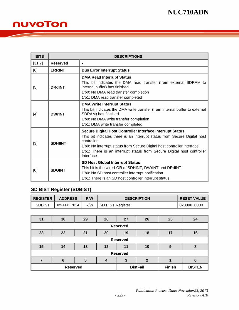
NUC710ADN
Publication Release Date: November23, 2013 - 225 - Revision A10
BITS DESCRIPTIONS
[31:7] Reserved -
[6] ERRINT Bus Error Interrupt Status
[5] DRdINT
DMA Read Interrupt Status This bit indicates the DMA read transfer (from external SDRAM to internal buffer) has finished. 1’b0: No DMA read transfer completion 1’b1: DMA read transfer completed
[4] DWrINT
DMA Write Interrupt Status This bit indicates the DMA write transfer (from internal buffer to external SDRAM) has finished. 1’b0: No DMA write transfer completion 1’b1: DMA write transfer completed
[3] SDHIINT
Secure Digital Host Controller Interface Interrupt Status This bit indicates there is an interrupt status from Secure Digital host controller. 1’b0: No interrupt status from Secure Digital host controller interface. 1’b1: There is an interrupt status from Secure Digital host controller Interface
[0] SDGINT
SD Host Global Interrupt Status This bit is the wired-OR of SDHINT, DWrINT and DRdINT. 1’b0: No SD host controller interrupt notification 1’b1: There is an SD host controller interrupt status
SD BIST Register (SDBIST)
REGISTER ADDRESS R/W DESCRIPTION RESET VALUE
SDBIST 0xFFF0_7014 R/W SD BIST Register 0x0000_0000
31 30 29 28 27 26 25 24
Reserved
23 22 21 20 19 18 17 16
Reserved
15 14 13 12 11 10 9 8
Reserved
7 6 5 4 3 2 1 0
Reserved BistFail Finish BISTEN
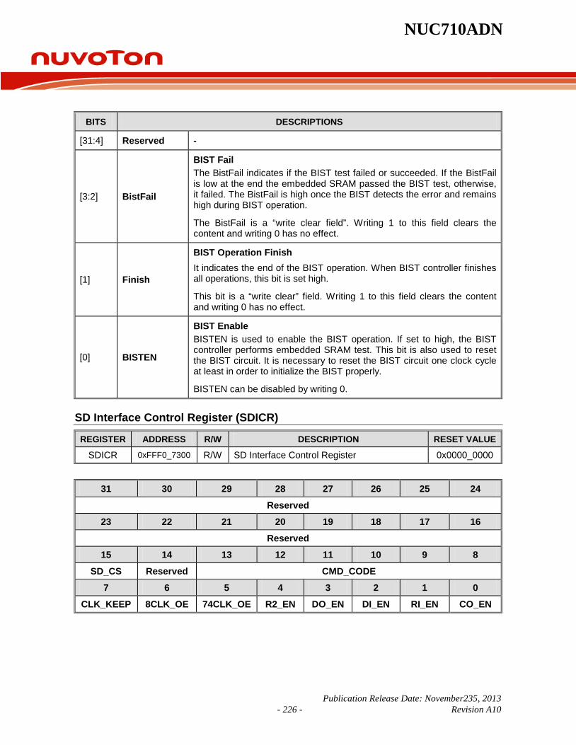
NUC710ADN
Publication Release Date: November235, 2013 - 226 - Revision A10
BITS DESCRIPTIONS
[31:4] Reserved -
[3:2] BistFail
BIST Fail The BistFail indicates if the BIST test failed or succeeded. If the BistFail is low at the end the embedded SRAM passed the BIST test, otherwise, it failed. The BistFail is high once the BIST detects the error and remains high during BIST operation.
The BistFail is a “write clear field”. Writing 1 to this field clears the content and writing 0 has no effect.
[1] Finish
BIST Operation Finish It indicates the end of the BIST operation. When BIST controller finishes all operations, this bit is set high.
This bit is a “write clear” field. Writing 1 to this field clears the content and writing 0 has no effect.
[0] BISTEN
BIST Enable BISTEN is used to enable the BIST operation. If set to high, the BIST controller performs embedded SRAM test. This bit is also used to reset the BIST circuit. It is necessary to reset the BIST circuit one clock cycle at least in order to initialize the BIST properly.
BISTEN can be disabled by writing 0.
SD Interface Control Register (SDICR)
REGISTER ADDRESS R/W DESCRIPTION RESET VALUE
SDICR 0xFFF0_7300 R/W SD Interface Control Register 0x0000_0000
31 30 29 28 27 26 25 24
Reserved
23 22 21 20 19 18 17 16
Reserved
15 14 13 12 11 10 9 8
SD_CS Reserved CMD_CODE
7 6 5 4 3 2 1 0
CLK_KEEP 8CLK_OE 74CLK_OE R2_EN DO_EN DI_EN RI_EN CO_EN

NUC710ADN
Publication Release Date: November23, 2013 - 227 - Revision A10
BITS DESCRIPTIONS
[31:16] Reserved -
[15] SD_CS
SD Card Select Control 0=Select SD card-0 1=Select SD card-1 It is fixed to 0 at NUC710
[13:8] CMD_CODE SD Command Code This register contains the SD command code (00H – 3FH).
[7] CLK_KEEP SD Clock Enable 0=Disable SD clock generation 1=SD clock always keeps free running.
[6] 8CLK_OE
8 Clock Cycles Output Enable 0=Disable 1=Enable, SD host controller output 8 clock cycles When the operation is finished, this bit is automatically cleared to 0 via H/W circuit.
[5] 74CLK_OE
74 Clock Cycle Output Enable 0=Disable 1=Enable, SD host controller outputs 74 clock cycles When the operation is finished, this bit is automatically cleared to 0 via H/W circuit.
[4] R2_EN
Response R2 Input Enable 0=Disable 1=Enable, SD host controller will wait to receive a response R2 from DS card and store the response data into flash buffer. When the R2 response operation is finished, this bit is automatically cleared to 0 via H/W circuit.
[3] DO_EN
Data Output Enable 0=Disable 1=Enable, SD host controller will transfer a single data block and the CRC-16 code to the SD card. When the data output operation is finished, this bit is automatically cleared to 0 via H/W circuit.
[2] DI_EN
Data Input Enable 0=Disable 1=Enable, SD host controller will wait to receive a single data block and the CRC-16 code from SD card. When the data input operation is finished, this bit is automatically cleared to 0 by H/W circuit.
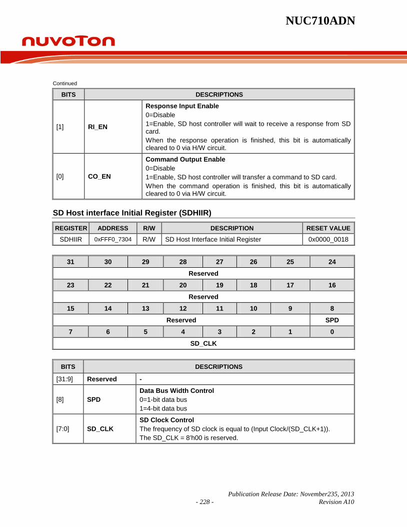
NUC710ADN
Publication Release Date: November235, 2013 - 228 - Revision A10
Continued
BITS DESCRIPTIONS
[1] RI_EN
Response Input Enable 0=Disable 1=Enable, SD host controller will wait to receive a response from SD card. When the response operation is finished, this bit is automatically cleared to 0 via H/W circuit.
[0] CO_EN
Command Output Enable 0=Disable 1=Enable, SD host controller will transfer a command to SD card. When the command operation is finished, this bit is automatically cleared to 0 via H/W circuit.
SD Host interface Initial Register (SDHIIR)
REGISTER ADDRESS R/W DESCRIPTION RESET VALUE
SDHIIR 0xFFF0_7304 R/W SD Host Interface Initial Register 0x0000_0018
31 30 29 28 27 26 25 24
Reserved
23 22 21 20 19 18 17 16
Reserved
15 14 13 12 11 10 9 8
Reserved SPD
7 6 5 4 3 2 1 0
SD_CLK
BITS DESCRIPTIONS
[31:9] Reserved -
[8] SPD Data Bus Width Control 0=1-bit data bus 1=4-bit data bus
[7:0] SD_CLK SD Clock Control The frequency of SD clock is equal to (Input Clock/(SD_CLK+1)). The SD_CLK = 8’h00 is reserved.

NUC710ADN
Publication Release Date: November23, 2013 - 229 - Revision A10
SD Interface Interrupt Enable Register (SDIIER)
REGISTER ADDRESS R/W DESCRIPTION RESET VALUE
SDIIER 0xFFF0_7308 R/W SD Interface Interrupt Enable Register 0x0000_0000
31 30 29 28 27 26 25 24
Reserved
23 22 21 20 19 18 17 16
Reserved
15 14 13 12 11 10 9 8
Reserved
7 6 5 4 3 2 1 0
Reserved SD_IEN DAT0_IEN CD_IEN DO_IEN DI_IEN
BITS DESCRIPTIONS
[31:5] Reserved -
[4] SD_IEN SD Interrupt Status Enable 0=Disable SD_IS interrupt generation 1=Enable SD_IS interrupt generation
[3] DAT0_IEN SD DAT0 Level Transition Interrupt Status Enable 0=Disable DAT0_STS interrupt generation 1=Enable DAT0_STS interrupt generation
[2] CD_IEN CD# Interrupt Status Enable 0=Disable CD_IS interrupt generation 1=Enable CD_IS interrupt generation
[1] DO_IEN Data Output Interrupt Status Enable 0=Disable DO_IS interrupt generation 1=Enable DO_IS interrupt generation
[0] DI_IEN
Data Input Interrupt Status Enable
0=Disable DI_IS interrupt generation 1=Enable DI_IS interrupt generation

NUC710ADN
Publication Release Date: November235, 2013 - 230 - Revision A10
SD Interface Interrupt Status Register (SDIISR)
REGISTER ADDRESS R/W DESCRIPTION RESET VALUE
SDISR 0xFFF0_730C R/W SD Interface Interrupt Status Register 0x0000_00XX
31 30 29 28 27 26 25 24 Reserved
23 22 21 20 19 18 17 16 Reserved
15 14 13 12 11 10 9 8 Reserved DAT1_IS_ SD_DATA0 DAT0_STS
7 6 5 4 3 2 1 0 CD_ R2_CRC7 CRC CRC-16 CRC-7 CD_IS DO_IS DI_IS
BITS DESCRIPTIONS
[31:11] Reserved -
[10] DAT1_IS_
SD Interrupt Value Status 0 = SD interrupt at interrupt period. Write 1 to clear this status bit (set DAT1_IS_ to 1). 1 = no SD interrupt at interrupt period. If SD_IEN is set and DAT1_IS_ is 0, an interrupt request is generated. Interrupt period is defined: (1) If SD data bus width is 1 and DAT[1] is unused, the interrupt
period is any time on DAT[1] (2) If SD data bus width is 4, the interrupt period is at the single clock
that is 2 clocks after the End bit of data block
[9] SD_DATA0 SD DAT0 Value
[8] DAT0_STS
SD Level Transition Status 0=No level transition 1=DAT0 value changes from high to low or low to high. Write 1 to clear this status bit.
[7] CD_ Card Detection Indicator
[6] R2_CRC7 Response R2 CRC-7 Check Status 0=Fault 1=OK
[5] CRC CRC Check Result Status 0=Fault 1=OK

NUC710ADN
Publication Release Date: November23, 2013 - 231 - Revision A10
Continued.
BITS DESCRIPTIONS
[4] CRC-16 CRC-16 Check Result Status 0=Fault 1=OK
[3] CRC-7 CRC-7 Check Result Status 0=Fault 1=OK
[2] CD_IS
CD# Interrupt Status 0=No Interrupt Generated 1=Interrupt Generated Note: Writing 1 to this bit will clear the interrupt status.
[1] DO_IS
Data Output Interrupt Status 0=No Interrupt Generated 1=Interrupt Generated Note: Writing 1 to this bit will clear the interrupt status.
[0] DI_IS
Data Input Interrupt Status 0=No Interrupt Generated 1=Interrupt Generated Note: Writing 1 to this bit will clear the interrupt status.
SD Command Argument Register (SDAUG)
REGISTER ADDRESS R/W DESCRIPTION RESET VALUE
SDAUG 0xFFF0_7310 R/W SD Command Argument Register 0x0000_0000
31 30 29 28 27 26 25 24 SD_CMD_ARG
23 22 21 20 19 18 17 16 SD_CMD_ARG
15 14 13 12 11 10 9 8 SD_CMD_ARG
7 6 5 4 3 2 1 0 SD_CMD_ARG
BITS DESCRIPTIONS
[31:0] SD_CMD_ARG SD Command Argument This register contains a 32-bit value specifying the argument of the SD command from host controller.
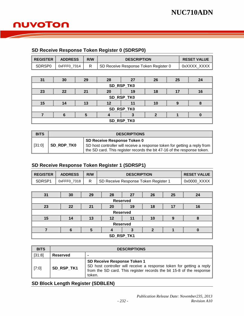
NUC710ADN
Publication Release Date: November235, 2013 - 232 - Revision A10
SD Receive Response Token Register 0 (SDRSP0)
REGISTER ADDRESS R/W DESCRIPTION RESET VALUE
SDRSP0 0xFFF0_7314 R SD Receive Response Token Register 0 0xXXXX_XXXX
31 30 29 28 27 26 25 24 SD_RSP_TK0
23 22 21 20 19 18 17 16 SD_RSP_TK0
15 14 13 12 11 10 9 8 SD_RSP_TK0
7 6 5 4 3 2 1 0 SD_RSP_TK0
BITS DESCRIPTIONS
[31:0] SD_RDP_TK0 SD Receive Response Token 0 SD host controller will receive a response token for getting a reply from the SD card. This register records the bit 47-16 of the response token.
SD Receive Response Token Register 1 (SDRSP1)
REGISTER ADDRESS R/W DESCRIPTION RESET VALUE
SDRSP1 0xFFF0_7318 R SD Receive Response Token Register 1 0x0000_XXXX
31 30 29 28 27 26 25 24 Reserved
23 22 21 20 19 18 17 16 Reserved
15 14 13 12 11 10 9 8 Reserved
7 6 5 4 3 2 1 0 SD_RSP_TK1
BITS DESCRIPTIONS [31:8] Reserved -
[7:0] SD_RSP_TK1 SD Receive Response Token 1 SD host controller will receive a response token for getting a reply from the SD card. This register records the bit 15-8 of the response token.
SD Block Length Register (SDBLEN)
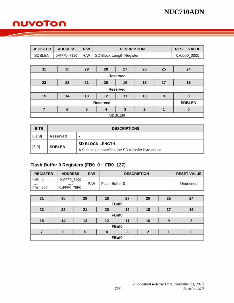
NUC710ADN
Publication Release Date: November23, 2013 - 233 - Revision A10
REGISTER ADDRESS R/W DESCRIPTION RESET VALUE
SDBLEN 0xFFF0_731C R/W SD Block Length Register 0x0000_0000
31 30 29 28 27 26 25 24
Reserved
23 22 21 20 19 18 17 16
Reserved
15 14 13 12 11 10 9 8
Reserved SDBLEN
7 6 5 4 3 2 1 0 SDBLEN
BITS DESCRIPTIONS
[31:9] Reserved -
[8:0] SDBLEN SD BLOCK LENGTH A 9-bit value specifies the SD transfer byte count.
Flash Buffer 0 Registers (FB0_0 ~ FB0_127)
REGISTER ADDRESS R/W DESCRIPTION RESET VALUE FB0_0 ….. FB0_127
0xFFF0_7400 …..
0xFFF0_75FC R/W Flash Buffer 0 Undefined
31 30 29 28 27 26 25 24
FBuf0 23 22 21 20 19 18 17 16
FBuf0 15 14 13 12 11 10 9 8
FBuf0 7 6 5 4 3 2 1 0
FBuf0
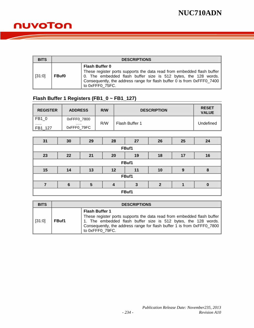
NUC710ADN
Publication Release Date: November235, 2013 - 234 - Revision A10
BITS DESCRIPTIONS
[31:0] FBuf0
Flash Buffer 0 These register ports supports the data read from embedded flash buffer 0. The embedded flash buffer size is 512 bytes, the 128 words. Consequently, the address range for flash buffer 0 is from 0xFFF0_7400 to 0xFFF0_75FC.
Flash Buffer 1 Registers (FB1_0 ~ FB1_127)
REGISTER ADDRESS R/W DESCRIPTION RESET VALUE
FB1_0 ….. FB1_127
0xFFF0_7800 …..
0xFFF0_79FC R/W Flash Buffer 1 Undefined
31 30 29 28 27 26 25 24
FBuf1
23 22 21 20 19 18 17 16
FBuf1
15 14 13 12 11 10 9 8 FBuf1
7 6 5 4 3 2 1 0
FBuf1
BITS DESCRIPTIONS
[31:0] FBuf1
Flash Buffer 1 These register ports supports the data read from embedded flash buffer 1. The embedded flash buffer size is 512 bytes, the 128 words. Consequently, the address range for flash buffer 1 is from 0xFFF0_7800 to 0xFFF0_79FC.
NUC710ADN
Publication Release Date: November23, 2013 - 235 - Revision A10
6.10 LCD Controller 6.10.1 Main Features STN LCD Display Supports 4-bit single scan Monochrome STN LCD panel, 8-bit single scan Monochrome STN LCD
panel, 8-bit single scan Color STN LCD panel (all Sync-type) Up to 16 gray level display for Monochrome STN LCD panel Up to 4096 (12bpp) color display for Color STN LCD panel Virtual coloring method: Frame Rate Control (16 levels) Anti-flickering method: Time-based Dithering
TFT LCD Display Supports Sync-type TFT LCD panel and Sync-type High-color TFT LCD panel Supports direct or palletized color display TV Encoder Supports 8-bit CCIR 601 YCbCr data output format to connect with external TV Encoder
LCD Preprocessing Supports RGB Raw-data or YUV422 packet format Programmable parameters for different image size Two Built-in FIFOs, FIFO 1 is for Video image and FIFO 2 is for OSD image. Each FIFO is 16
words deep
LCD Post processing Support for one OSD (On Screen Display) overlay Support various OSD function Programmable parameters for different display panels
Others Color lookup table size 256x32 bit for TFT used when displaying 1bpp, 2bpp, 4bpp, 8bpp image Dedicated DMA for block transfer mode

NUC710ADN
Publication Release Date: November235, 2013 - 236 - Revision A10
6.10.2 LCD Register MAP
REGISTER ADDRESS R/W DESCRIPTION RESET VALUE LCD Controller LCDCON 0XFFF0_8000 R/W LCD Control 0x0000_0000
LCD Interrupt Control LCDINTENB 0xFFF0_8004 R/W LCD Interrupt Enable 0x0000_0000
LCDINTS 0xFFF0_8008 R LCD Interrupt Status 0x0000_0000
LCDINTC 0xFFF0_800C W LCD Interrupt Clear 0x0000_0000
LCD Pre-processing
OSDUPSCF 0xFFF0_8010 R/W OSD Horizontal/Vertical upscaling factor 0x0000_0000
VDUPSCF 0xFFF0_8014 R/W Video Horizontal/Vertical upscaling factor 0x0000_0000
OSDDNSCF 0xFFF0_8018 R/W OSD Horizontal/Vertical Downscaling factor 0x0000_0000
VDDNSCF 0xFFF0_801C R/W Video Horizontal/Vertical Downscaling factor 0x0000_0000
LCD FIFO Control FIFOCON 0xFFF0_8020 R/W FIFOs control 0x0000_0000
FIFOSTATUS 0xFFF0_8024 R FIFOs status 0x0000_0000
FIFO1PRM 0xFFF0_8028 R/W FIFO1 parameters 0x0000_0000
FIFO2PRM 0xFFF0_802C R/W FIFO2 parameters 0x0000_0000
FIFO1SADDR 0xFFF0_8030 R/W FIFO1 start address 0x0000_0000
FIFO2SADDR 0xFFF0_8034 R/W FIFO2 start address 0x0000_0000
FIFO1DREQCNT 0xFFF0_8038 R/W FIFO1 data request count 0x0000_0000
FIFO2DREQCNT 0xFFF0_803C R/W FIFO2 data request count 0x0000_0000
FIFO1CURADR 0xFFF0_8040 R FIFO1 current access address 0x0000_0000
FIFO2CURADR 0xFFF0_8044 R FIFO2 current access address 0x0000_0000
FIFO1RELACOLCNT 0xFFF0_8048 R/W FIFO1 real column count 0x0000_0000
FIFO2RELACOLCNT 0xFFF0_804C R/W FIFO2 real column count 0x0000_0000
Color Generation
VDLUTENTRY1 0xFFF0_8050 R/W Video lookup table entry index 1 0x0000_0000
VDLUTENTRY2 0xFFF0_8054 R/W Video lookup table entry index 2 0x0000_0000
VDLUTENTRY3 0xFFF0_8058 R/W Video lookup table entry index 3 0x0000_0000
VDLUTENTRY4 0xFFF0_805C R/W Video lookup table entry index 4 0x0000_0000
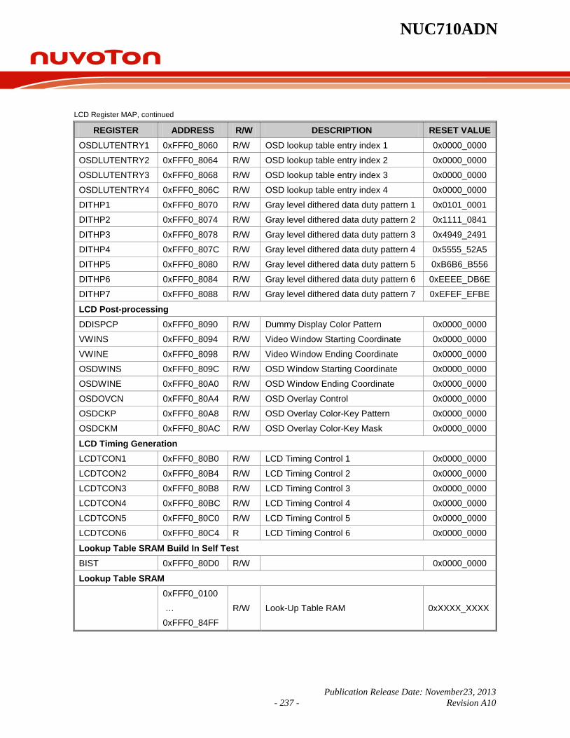
NUC710ADN
Publication Release Date: November23, 2013 - 237 - Revision A10
LCD Register MAP, continued
REGISTER ADDRESS R/W DESCRIPTION RESET VALUE OSDLUTENTRY1 0xFFF0_8060 R/W OSD lookup table entry index 1 0x0000_0000
OSDLUTENTRY2 0xFFF0_8064 R/W OSD lookup table entry index 2 0x0000_0000
OSDLUTENTRY3 0xFFF0_8068 R/W OSD lookup table entry index 3 0x0000_0000
OSDLUTENTRY4 0xFFF0_806C R/W OSD lookup table entry index 4 0x0000_0000
DITHP1 0xFFF0_8070 R/W Gray level dithered data duty pattern 1 0x0101_0001
DITHP2 0xFFF0_8074 R/W Gray level dithered data duty pattern 2 0x1111_0841
DITHP3 0xFFF0_8078 R/W Gray level dithered data duty pattern 3 0x4949_2491
DITHP4 0xFFF0_807C R/W Gray level dithered data duty pattern 4 0x5555_52A5
DITHP5 0xFFF0_8080 R/W Gray level dithered data duty pattern 5 0xB6B6_B556
DITHP6 0xFFF0_8084 R/W Gray level dithered data duty pattern 6 0xEEEE_DB6E
DITHP7 0xFFF0_8088 R/W Gray level dithered data duty pattern 7 0xEFEF_EFBE
LCD Post-processing
DDISPCP 0xFFF0_8090 R/W Dummy Display Color Pattern 0x0000_0000
VWINS 0xFFF0_8094 R/W Video Window Starting Coordinate 0x0000_0000
VWINE 0xFFF0_8098 R/W Video Window Ending Coordinate 0x0000_0000
OSDWINS 0xFFF0_809C R/W OSD Window Starting Coordinate 0x0000_0000
OSDWINE 0xFFF0_80A0 R/W OSD Window Ending Coordinate 0x0000_0000
OSDOVCN 0xFFF0_80A4 R/W OSD Overlay Control 0x0000_0000
OSDCKP 0xFFF0_80A8 R/W OSD Overlay Color-Key Pattern 0x0000_0000
OSDCKM 0xFFF0_80AC R/W OSD Overlay Color-Key Mask 0x0000_0000
LCD Timing Generation
LCDTCON1 0xFFF0_80B0 R/W LCD Timing Control 1 0x0000_0000
LCDTCON2 0xFFF0_80B4 R/W LCD Timing Control 2 0x0000_0000
LCDTCON3 0xFFF0_80B8 R/W LCD Timing Control 3 0x0000_0000
LCDTCON4 0xFFF0_80BC R/W LCD Timing Control 4 0x0000_0000
LCDTCON5 0xFFF0_80C0 R/W LCD Timing Control 5 0x0000_0000
LCDTCON6 0xFFF0_80C4 R LCD Timing Control 6 0x0000_0000
Lookup Table SRAM Build In Self Test BIST 0xFFF0_80D0 R/W 0x0000_0000
Lookup Table SRAM
0xFFF0_0100 … 0xFFF0_84FF
R/W Look-Up Table RAM 0xXXXX_XXXX
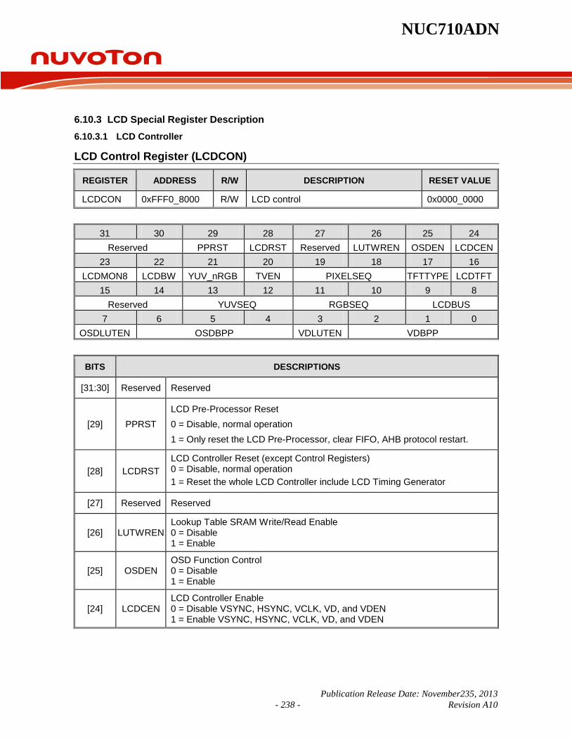
NUC710ADN
Publication Release Date: November235, 2013 - 238 - Revision A10
6.10.3 LCD Special Register Description 6.10.3.1 LCD Controller
LCD Control Register (LCDCON)
REGISTER ADDRESS R/W DESCRIPTION RESET VALUE
LCDCON 0xFFF0_8000 R/W LCD control 0x0000_0000
31 30 29 28 27 26 25 24 Reserved PPRST LCDRST Reserved LUTWREN OSDEN LCDCEN
23 22 21 20 19 18 17 16 LCDMON8 LCDBW YUV_nRGB TVEN PIXELSEQ TFTTYPE LCDTFT
15 14 13 12 11 10 9 8 Reserved YUVSEQ RGBSEQ LCDBUS
7 6 5 4 3 2 1 0 OSDLUTEN OSDBPP VDLUTEN VDBPP
BITS DESCRIPTIONS
[31:30] Reserved Reserved
[29] PPRST LCD Pre-Processor Reset 0 = Disable, normal operation 1 = Only reset the LCD Pre-Processor, clear FIFO, AHB protocol restart.
[28] LCDRST LCD Controller Reset (except Control Registers) 0 = Disable, normal operation 1 = Reset the whole LCD Controller include LCD Timing Generator
[27] Reserved Reserved
[26] LUTWREN Lookup Table SRAM Write/Read Enable 0 = Disable 1 = Enable
[25] OSDEN OSD Function Control 0 = Disable 1 = Enable
[24] LCDCEN LCD Controller Enable 0 = Disable VSYNC, HSYNC, VCLK, VD, and VDEN 1 = Enable VSYNC, HSYNC, VCLK, VD, and VDEN
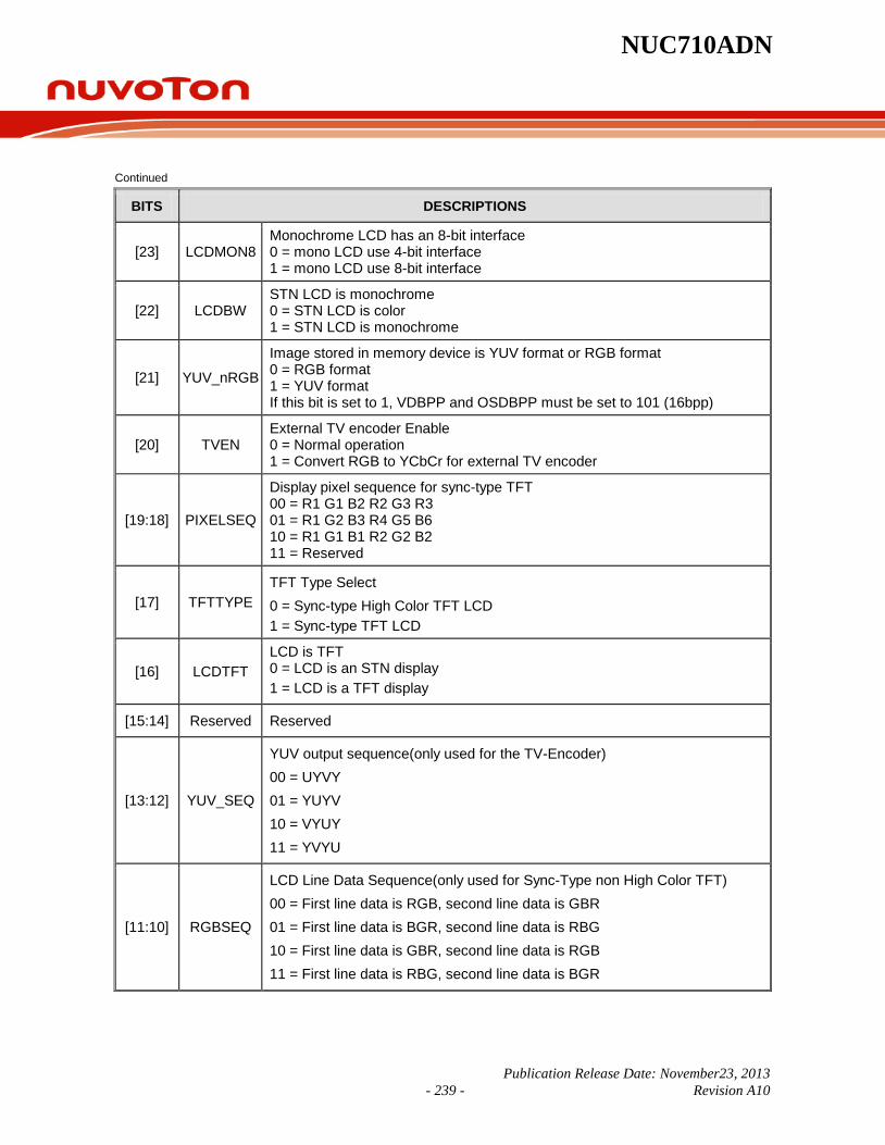
NUC710ADN
Publication Release Date: November23, 2013 - 239 - Revision A10
Continued
BITS DESCRIPTIONS
[23] LCDMON8 Monochrome LCD has an 8-bit interface 0 = mono LCD use 4-bit interface 1 = mono LCD use 8-bit interface
[22] LCDBW STN LCD is monochrome 0 = STN LCD is color 1 = STN LCD is monochrome
[21] YUV_nRGB
Image stored in memory device is YUV format or RGB format 0 = RGB format 1 = YUV format If this bit is set to 1, VDBPP and OSDBPP must be set to 101 (16bpp)
[20] TVEN External TV encoder Enable 0 = Normal operation 1 = Convert RGB to YCbCr for external TV encoder
[19:18] PIXELSEQ
Display pixel sequence for sync-type TFT 00 = R1 G1 B2 R2 G3 R3 01 = R1 G2 B3 R4 G5 B6 10 = R1 G1 B1 R2 G2 B2 11 = Reserved
[17] TFTTYPE TFT Type Select 0 = Sync-type High Color TFT LCD 1 = Sync-type TFT LCD
[16] LCDTFT LCD is TFT 0 = LCD is an STN display 1 = LCD is a TFT display
[15:14] Reserved Reserved
[13:12] YUV_SEQ
YUV output sequence(only used for the TV-Encoder) 00 = UYVY 01 = YUYV 10 = VYUY 11 = YVYU
[11:10] RGBSEQ
LCD Line Data Sequence(only used for Sync-Type non High Color TFT) 00 = First line data is RGB, second line data is GBR 01 = First line data is BGR, second line data is RBG 10 = First line data is GBR, second line data is RGB 11 = First line data is RBG, second line data is BGR
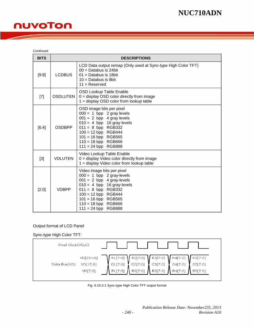
NUC710ADN
Publication Release Date: November235, 2013 - 240 - Revision A10
Continued
BITS DESCRIPTIONS
[9:8] LCDBUS
LCD Data output remap (Only used at Sync-type High Color TFT) 00 = Databus is 24bit 01 = Databus is 18bit 10 = Databus is 8bit 11 = Reserved
[7] OSDLUTEN OSD Lookup Table Enable 0 = display OSD color directly from image 1 = display OSD color from lookup table
[6:4] OSDBPP
OSD image bits per pixel 000 = 1 bpp 2 gray levels 001 = 2 bpp 4 gray levels 010 = 4 bpp 16 gray levels 011 = 8 bpp RGB332 100 = 12 bpp RGB444 101 = 16 bpp RGB565 110 = 18 bpp RGB666 111 = 24 bpp RGB888
[3] VDLUTEN Video Lookup Table Enable 0 = display Video color directly from image 1 = display Video color from lookup table
[2:0] VDBPP
Video image bits per pixel 000 = 1 bpp 2 gray-levels 001 = 2 bpp 4 gray-levels 010 = 4 bpp 16 gray-levels 011 = 8 bpp RGB332 100 = 12 bpp RGB444 101 = 16 bpp RGB565 110 = 18 bpp RGB666 111 = 24 bpp RGB888
Output format of LCD Panel
Sync-type High Color TFT:
Fig. 6.10.3.1 Sync-type High Color TFT output format
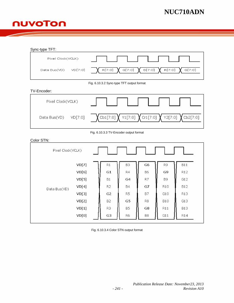
NUC710ADN
Publication Release Date: November23, 2013 - 241 - Revision A10
Sync-type TFT:
Fig. 6.10.3.2 Sync-type TFT output format
TV-Encoder:
Fig. 6.10.3.3 TV-Encoder output format
Color STN:
Fig. 6.10.3.4 Color STN output format

NUC710ADN
Publication Release Date: November235, 2013 - 242 - Revision A10
Monochrome STN with 4-bit data bus:
Fig. 6.10.3.5 Monochrome STN output format - 1
Monochrome STN with 8-bit data bus:
Fig. 6.10.3.6 Monochrome STN output format - 2
Only when LUTWREN is enabled, Lookup Table SRAM can be read or written by the CPU. If LUTWREN is disabled, the SRAM Lookup Table is accessed by the LCD Controller.
Palette function can’t be enabled for STN panel. Because the SRAM Lookup Table is only 256 x32 bits, so if either the Video or OSD image is 8bpp, both VDLUTEN and OSDLUTEN can only be enabled when the Video Palette Table is the same as the OSD.
If VDLUTEN or OSDLUTEN is enabled, the LCD Controller will output data from the SRAM Lookup Table for 8bpp, 4bpp, 2bpp, 1bpp image. Otherwise the LCD Controller treats 8bpp data as RGB332, 4bpp as 16 gray levels, 2bpp as 4 gray levels, 1bpp as 2 gray levels (black and white).
Normally, the LCD Databus output is RGB888, 24-bit. If the LCDBUS is set to 01, the LCD Databus output is RGB666, 18-bit. If the LCDBUS is set to 10, the LCD Databus output is RGB332, 8-bit. The other bit is replaced with zero. Please refer to GPIO chapter to setting this register. This is only used
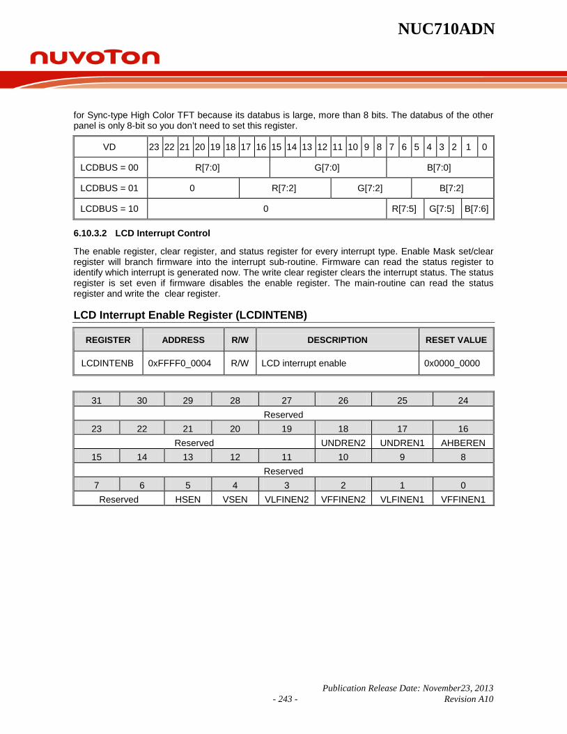
NUC710ADN
Publication Release Date: November23, 2013 - 243 - Revision A10
for Sync-type High Color TFT because its databus is large, more than 8 bits. The databus of the other panel is only 8-bit so you don’t need to set this register.
VD 23 22 21 20 19 18 17 16 15 14 13 12 11 10 9 8 7 6 5 4 3 2 1 0
LCDBUS = 00 R[7:0] G[7:0] B[7:0]
LCDBUS = 01 0 R[7:2] G[7:2] B[7:2]
LCDBUS = 10 0 R[7:5] G[7:5] B[7:6]
6.10.3.2 LCD Interrupt Control
The enable register, clear register, and status register for every interrupt type. Enable Mask set/clear register will branch firmware into the interrupt sub-routine. Firmware can read the status register to identify which interrupt is generated now. The write clear register clears the interrupt status. The status register is set even if firmware disables the enable register. The main-routine can read the status register and write the clear register.
LCD Interrupt Enable Register (LCDINTENB)
REGISTER ADDRESS R/W DESCRIPTION RESET VALUE
LCDINTENB 0xFFFF0_0004 R/W LCD interrupt enable 0x0000_0000
31 30 29 28 27 26 25 24 Reserved
23 22 21 20 19 18 17 16 Reserved UNDREN2 UNDREN1 AHBEREN
15 14 13 12 11 10 9 8 Reserved
7 6 5 4 3 2 1 0 Reserved HSEN VSEN VLFINEN2 VFFINEN2 VLFINEN1 VFFINEN1
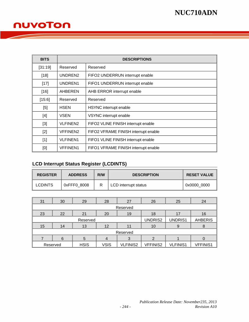
NUC710ADN
Publication Release Date: November235, 2013 - 244 - Revision A10
BITS DESCRIPTIONS
[31:19] Reserved Reserved
[18] UNDREN2 FIFO2 UNDERRUN interrupt enable
[17] UNDREN1 FIFO1 UNDERRUN interrupt enable
[16] AHBEREN AHB ERROR interrupt enable
[15:6] Reserved Reserved
[5] HSEN HSYNC interrupt enable
[4] VSEN VSYNC interrupt enable
[3] VLFINEN2 FIFO2 VLINE FINISH interrupt enable
[2] VFFINEN2 FIFO2 VFRAME FINISH interrupt enable
[1] VLFINEN1 FIFO1 VLINE FINISH interrupt enable
[0] VFFINEN1 FIFO1 VFRAME FINISH interrupt enable
LCD Interrupt Status Register (LCDINTS)
REGISTER ADDRESS R/W DESCRIPTION RESET VALUE
LCDINTS 0xFFF0_8008 R LCD interrupt status 0x0000_0000
31 30 29 28 27 26 25 24 Reserved
23 22 21 20 19 18 17 16 Reserved UNDRIS2 UNDRIS1 AHBERIS
15 14 13 12 11 10 9 8 Reserved
7 6 5 4 3 2 1 0 Reserved HSIS VSIS VLFINIS2 VFFINIS2 VLFINIS1 VFFINIS1

NUC710ADN
Publication Release Date: November23, 2013 - 245 - Revision A10
BITS DESCRIPTIONS
[31:20] Reserved Reserved
[18] UNDRIS2 FIFO2 have no data for output to Panel
[17] UNDRIS1 FIFO1 have no data for output to Panel
[16] AHBERIS AHB master bus error status
[15:6] Reserved Reserved
[5] HSIS Timing Generator output a HSYNC pulse
[4] VSIS Timing Generator output a VSYNC pulse
[3] VLFINIS2 FIFO2 transfer one line stream complete
[2] VFFINIS2 FIFO2 transfer one frame stream complete
[1] VLFINIS1 FIFO1 transfer one line stream complete
[0] VFFINIS1 FIFO1 transfer one frame stream complete
LCD Controller is an AHB Master at AMBA and fetching video data from an AHB Slave such as SDRAM or FLASH memory. If the AHB Slave response ERROR for LCD Controller’s data request, AHBERIS is set. If the data rate of the output to the LCD Panel is too fast and the data rate of fetch data from AMBA is too slow, there is no data in the FIFO for the LCD Panel’s request, UNDRISx is set. LCD Timing Generation register needs to be re-configured. HSIS and VSIS provide information for firmware to know the status of the LCD Panel. VLFINISx and VFFINISx provide information for firmware to know how much data FIFO has fetched.

NUC710ADN
Publication Release Date: November235, 2013 - 246 - Revision A10
LCD Interrupt Clear Register (LCDINTC)
REGISTER ADDRESS R/W DESCRIPTION RESET VALUE
LCDINTC 0xFFF0_800C W LCD interrupt clear 0x0000_0000
31 30 29 28 27 26 25 24 Reserved
23 22 21 20 19 18 17 16 Reserved UNDRIC2 UNDRIC1 AHBERIC
15 14 13 12 11 10 9 8 Reserved
7 6 5 4 3 2 1 0 Reserved HSIC VSIC VLFINIC2 VFFINIC2 VLFINIC1 VFFINIC1
BITS DESCRIPTIONS
[31:20] Reserved Reserved
[18] UNDRIC2 Clear FIFO2 UNDERRUN interrupt
[17] UNDRIC1 Clear FIFO1 UNDERRUN interrupt
[16] AHBERIC Clear MBERROR interrupt
[15:6] Reserved Reserved
[5] HSIC Clear HSYNC interrupt
[4] VSIC Clear VSYNC interrupt
[3] VLFINIC2 Clear FIFO2 VLINEFINSH interrupt
[2] VFFINIC2 Clear FIFO2 VFRAMFINSH interrupt
[1] VLFINIC1 Clear FIFO1 VLINEFINSH interrupt
[0] VFFINIC1 Clear FIFO1 VFRAMFINSH interrupt

NUC710ADN
Publication Release Date: November23, 2013 - 247 - Revision A10
6.10.3.3 LCD Pre-processing
OSD Upscaling Factor Register (OSDUPSCF)
REGISTER ADDRESS R/W DESCRIPTION RESET VALUE
OSDUPSCF 0xFFF0_8010 R/W OSD Horizontal/Vertical upscaling factor 0x0000_0000
31 30 29 28 27 26 25 24 Reserved
23 22 21 20 19 18 17 16 Reserved
15 14 13 12 11 10 9 8 Reserved
7 6 5 4 3 2 1 0 Reserved OSDHUP OSDVUP Reserved
BITS DESCRIPTIONS
[31:5] Reserved Reserved
[4:3] OSDHUP
OSD Stream Horizontal Upscaling 00=1x 01=2x 10=4x
[2:1] OSDVUP
OSD Stream Vertical Upscaling 00=1x 01=2x 10=4x
[0] Reserved Reserved
Video Upscaling Factor Register (VDUPSCF)
REGISTER ADDRESS R/W DESCRIPTION RESET VALUE
VDUPSCF 0xFFF0_8014 R/W Video Horizontal/Vertical upscaling
0x0000_0000
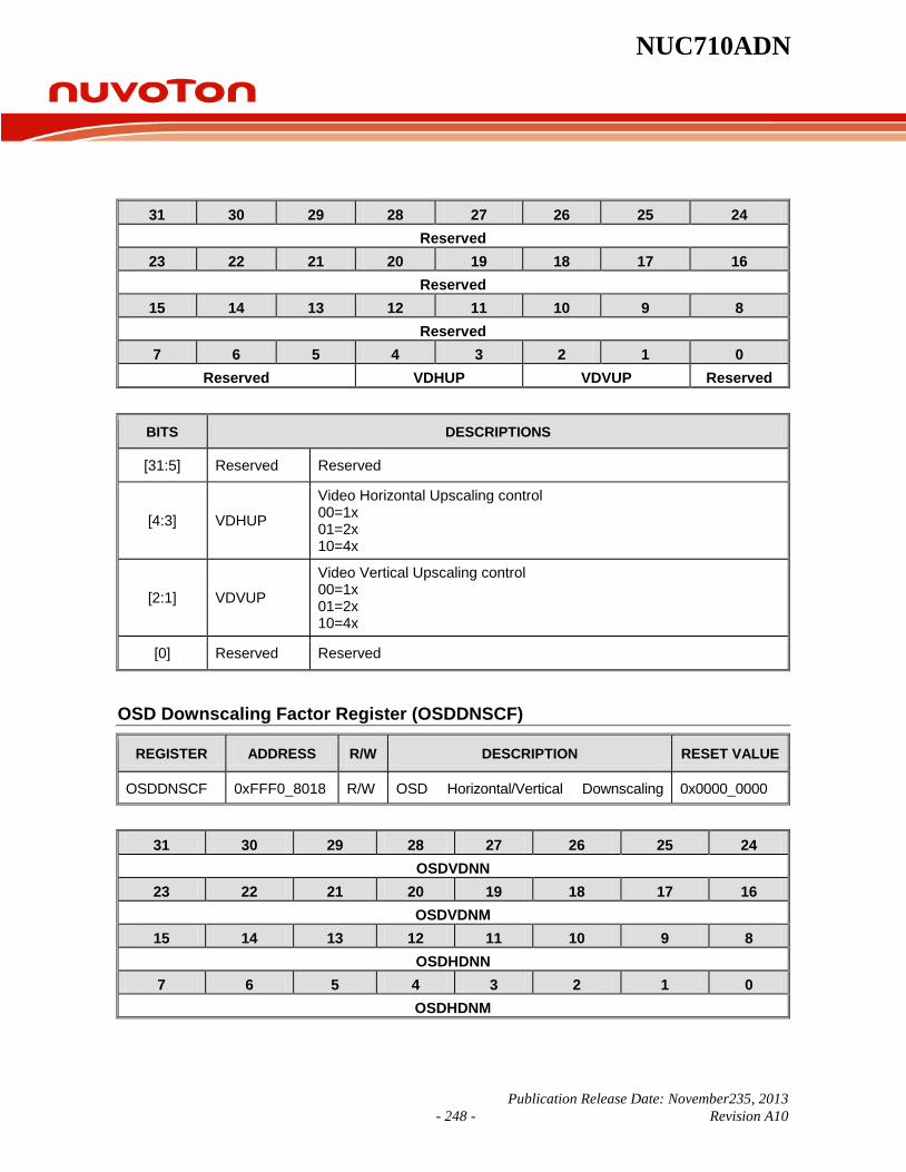
NUC710ADN
Publication Release Date: November235, 2013 - 248 - Revision A10
31 30 29 28 27 26 25 24 Reserved
23 22 21 20 19 18 17 16 Reserved
15 14 13 12 11 10 9 8 Reserved
7 6 5 4 3 2 1 0 Reserved VDHUP VDVUP Reserved
BITS DESCRIPTIONS
[31:5] Reserved Reserved
[4:3] VDHUP
Video Horizontal Upscaling control 00=1x 01=2x 10=4x
[2:1] VDVUP
Video Vertical Upscaling control 00=1x 01=2x 10=4x
[0] Reserved Reserved
OSD Downscaling Factor Register (OSDDNSCF)
REGISTER ADDRESS R/W DESCRIPTION RESET VALUE
OSDDNSCF 0xFFF0_8018 R/W OSD Horizontal/Vertical Downscaling
0x0000_0000
31 30 29 28 27 26 25 24 OSDVDNN
23 22 21 20 19 18 17 16 OSDVDNM
15 14 13 12 11 10 9 8 OSDHDNN
7 6 5 4 3 2 1 0 OSDHDNM
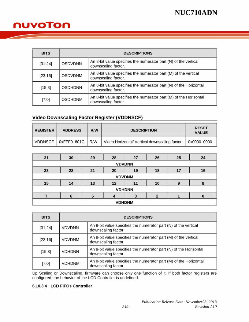
NUC710ADN
Publication Release Date: November23, 2013 - 249 - Revision A10
BITS DESCRIPTIONS
[31:24] OSDVDNN An 8-bit value specifies the numerator part (N) of the vertical downscaling factor.
[23:16] OSDVDNM An 8-bit value specifies the numerator part (M) of the vertical downscaling factor.
[15:8] OSDHDNN An 8-bit value specifies the numerator part (N) of the Horizontal downscaling factor.
[7:0] OSDHDNM An 8-bit value specifies the numerator part (M) of the Horizontal downscaling factor.
Video Downscaling Factor Register (VDDNSCF)
REGISTER ADDRESS R/W DESCRIPTION RESET VALUE
VDDNSCF 0xFFF0_801C R/W Video Horizontal/ Vertical downscaling factor 0x0000_0000
31 30 29 28 27 26 25 24 VDVDNN
23 22 21 20 19 18 17 16 VDVDNM
15 14 13 12 11 10 9 8 VDHDNN
7 6 5 4 3 2 1 0 VDHDNM
BITS DESCRIPTIONS
[31:24] VDVDNN An 8-bit value specifies the numerator part (N) of the vertical downscaling factor.
[23:16] VDVDNM An 8-bit value specifies the numerator part (M) of the vertical downscaling factor.
[15:8] VDHDNN An 8-bit value specifies the numerator part (N) of the Horizontal downscaling factor.
[7:0] VDHDNM An 8-bit value specifies the numerator part (M) of the Horizontal downscaling factor.
Up Scaling or Downscaling, firmware can choose only one function of it. If both factor registers are configured, the behavior of the LCD Controller is undefined.
6.10.3.4 LCD FIFOs Controller
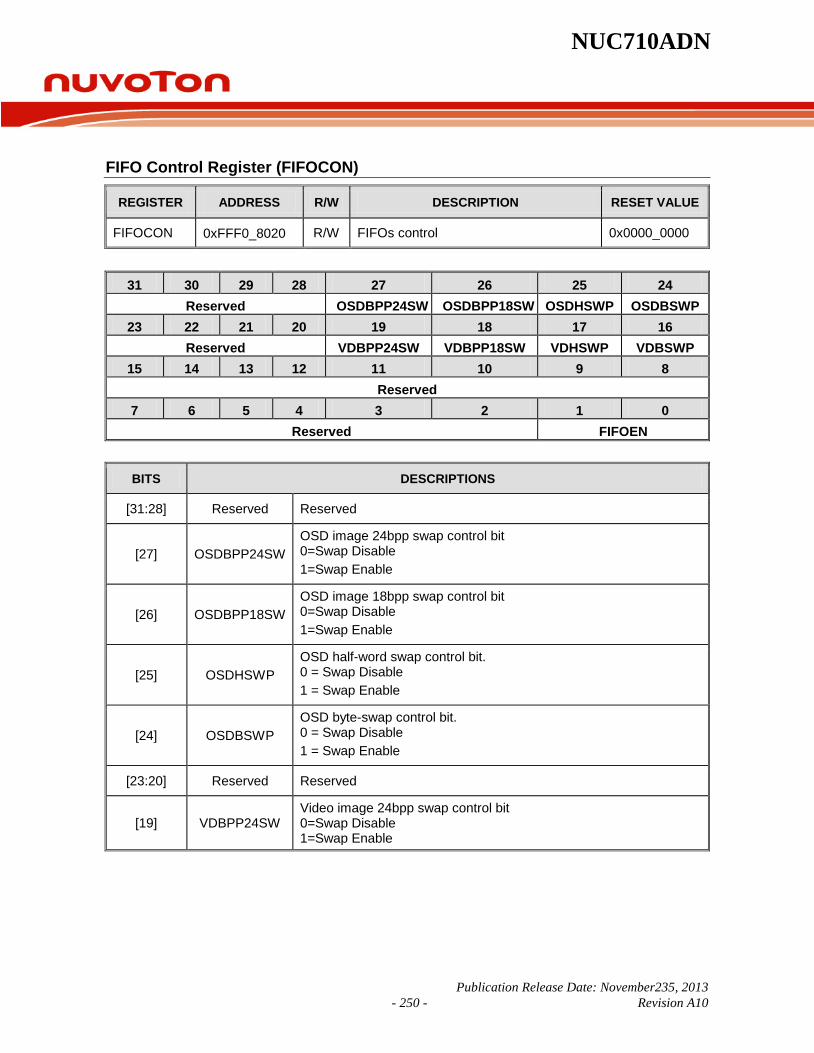
NUC710ADN
Publication Release Date: November235, 2013 - 250 - Revision A10
FIFO Control Register (FIFOCON)
REGISTER ADDRESS R/W DESCRIPTION RESET VALUE
FIFOCON 0xFFF0_8020 R/W FIFOs control 0x0000_0000
31 30 29 28 27 26 25 24 Reserved OSDBPP24SW OSDBPP18SW OSDHSWP OSDBSWP
23 22 21 20 19 18 17 16 Reserved VDBPP24SW VDBPP18SW VDHSWP VDBSWP
15 14 13 12 11 10 9 8 Reserved
7 6 5 4 3 2 1 0 Reserved FIFOEN
BITS DESCRIPTIONS
[31:28] Reserved Reserved
[27] OSDBPP24SW OSD image 24bpp swap control bit 0=Swap Disable 1=Swap Enable
[26] OSDBPP18SW OSD image 18bpp swap control bit 0=Swap Disable 1=Swap Enable
[25] OSDHSWP OSD half-word swap control bit. 0 = Swap Disable 1 = Swap Enable
[24] OSDBSWP OSD byte-swap control bit. 0 = Swap Disable 1 = Swap Enable
[23:20] Reserved Reserved
[19] VDBPP24SW Video image 24bpp swap control bit 0=Swap Disable 1=Swap Enable

NUC710ADN
Publication Release Date: November23, 2013 - 251 - Revision A10
Continued
BITS DESCRIPTIONS
[18] VDBPP18SW Video image 18bpp swap control bit 0=Swap Disable 1=Swap Enable
[17] VDHSWP Video half-word swap control bit. 0 = Swap Disable 1 = Swap Enable
[16] VDBSWP Video byte-swap control bit. 0 = Swap Disable 1 = Swap Enable
[15:2] Reserved Reserved
[1:0] FIFOEN FIFOs transfer data enable x1 = FIFO1 transfer enable x0=FIFO1 transfer disable 1x = FIFO2 transfer enable 0x=FIFO2 transfer disable
FIFO Status Register (FIFOSTATUS)
REGISTER ADDRESS R/W DESCRIPTION RESET VALUE
FIFOSTATUS 0xFFF0_8024 R FIFOs status 0x0000_0000
31 30 29 28 27 26 25 24 Reserved
23 22 21 20 19 18 17 16 Reserved
15 14 13 12 11 10 9 8 Reserved
7 6 5 4 3 2 1 0 Reserved MASTERID
BITS DESCRIPTIONS
[31:2] Reserved Reserved
[1:0] MASTERID Currently, the data bus master 01 = FIFO1 grant the bus 11 = FIFO2 grant the bus
FIFO1 Parameter Register (FIFO1PRM)

NUC710ADN
Publication Release Date: November235, 2013 - 252 - Revision A10
REGISTER ADDRESS R/W DESCRIPTION RESET VALUE
FIFO1PRM 0xFFF0_8028 R/W FIFO1 parameters 0x0000_0000
31 30 29 28 27 26 25 24 F1STRIDE[15:8]
23 22 21 20 19 18 17 16 F1STRIDE[7:0]
15 14 13 12 11 10 9 8 Reserved
7 6 5 4 3 2 1 0 Reserved F1LOCK F1BURSTY F1TRANSZ
BITS DESCRIPTIONS
[31:16] F1STRIDE Video frame buffer stride 16-bit value specifies the word offset of memory address of vertically adjacent line for FIFO1 fetching.
[15:5] Reserved Reserved
[4] F1LOCK FIFO1 lock transfer enable 0 = Disable 1 = Enable
[3:2] F1BURSTY
FIFO1 burst transfer type 00 =4 data burst mode 01 =8 data burst mode 10 =16 data burst mode
[1:0] F1TRANSZ
FIFO1 data width per-transfer 00=one byte 01=half word 10=one word
FIFO2 Parameter Register (FIFO2PRM)
REGISTER ADDRESS R/W DESCRIPTION RESET VALUE
FIFO2PRM 0xFFF0_802C R/W FIFO2 parameters 0x0000_0000
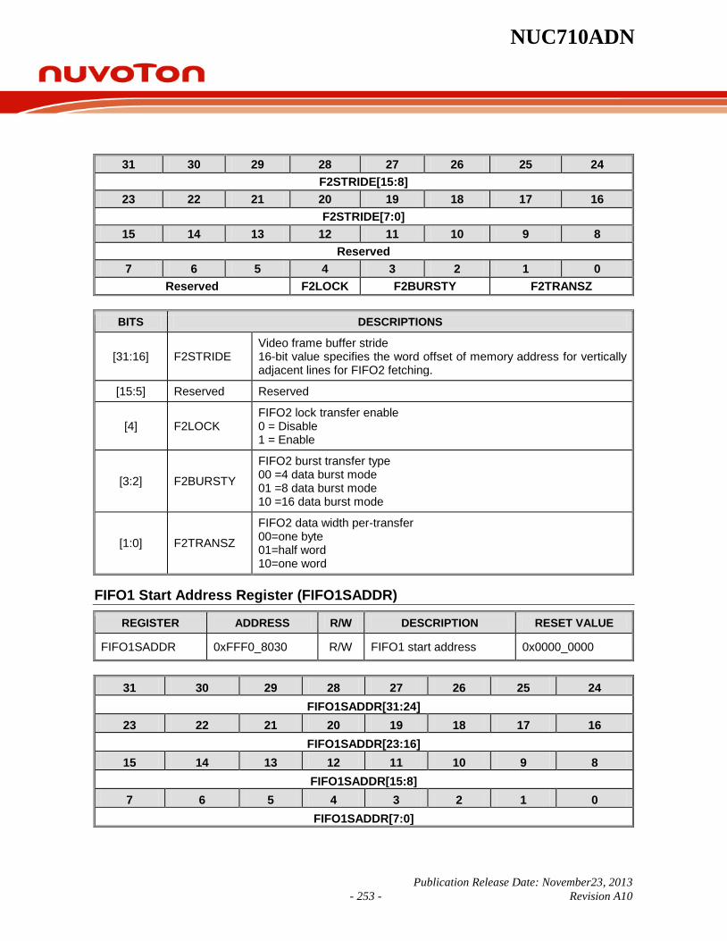
NUC710ADN
Publication Release Date: November23, 2013 - 253 - Revision A10
31 30 29 28 27 26 25 24
F2STRIDE[15:8] 23 22 21 20 19 18 17 16
F2STRIDE[7:0] 15 14 13 12 11 10 9 8
Reserved 7 6 5 4 3 2 1 0
Reserved F2LOCK F2BURSTY F2TRANSZ
BITS DESCRIPTIONS
[31:16] F2STRIDE Video frame buffer stride 16-bit value specifies the word offset of memory address for vertically adjacent lines for FIFO2 fetching.
[15:5] Reserved Reserved
[4] F2LOCK FIFO2 lock transfer enable 0 = Disable 1 = Enable
[3:2] F2BURSTY
FIFO2 burst transfer type 00 =4 data burst mode 01 =8 data burst mode 10 =16 data burst mode
[1:0] F2TRANSZ
FIFO2 data width per-transfer 00=one byte 01=half word 10=one word
FIFO1 Start Address Register (FIFO1SADDR)
REGISTER ADDRESS R/W DESCRIPTION RESET VALUE
FIFO1SADDR 0xFFF0_8030 R/W FIFO1 start address 0x0000_0000
31 30 29 28 27 26 25 24
FIFO1SADDR[31:24] 23 22 21 20 19 18 17 16
FIFO1SADDR[23:16] 15 14 13 12 11 10 9 8
FIFO1SADDR[15:8] 7 6 5 4 3 2 1 0
FIFO1SADDR[7:0]

NUC710ADN
Publication Release Date: November235, 2013 - 254 - Revision A10
BITS DESCRIPTIONS
[31:0] FIFO1SADDR These bits indicate the source address of the bank location for the LCD frame buffer in system memory.
FIFO2 Start Address Register (FIFO2SADDR)
REGISTER ADDRESS R/W DESCRIPTION RESET VALUE
FIFO2SADDR 0xFFF0_8034 R/W FIFO2 start address 0x0000_0000
31 30 29 28 27 26 25 24 FIFO2SADDR[31:24]
23 22 21 20 19 18 17 16 FIFO2SADDR[23:16]
15 14 13 12 11 10 9 8 FIFO2SADDR[15:8]
7 6 5 4 3 2 1 0 FIFO2SADDR[7:0]
BITS DESCRIPTIONS
[31:0] FIFO2SADDR These bits indicate the source address of the bank location for the LCD frame buffer in system memory.
FIFO1 Request Count Register (FIFO1DREQCNT)
REGISTER ADDRESS R/W DESCRIPTION RESET VALUE
FIFO1DREQCNT 0xFFF0_8038 R/W FIFO1 request count 0x0000_0000
31 30 29 28 27 26 25 24
FIFO1COLCNT[31:24] 23 22 21 20 19 18 17 16
FIFO1COLCNT[23:16] 15 14 13 12 11 10 9 8
FIFO1ROWCNT[15:8] 7 6 5 4 3 2 1 0
FIFO1ROWCNT[7:0]

NUC710ADN
Publication Release Date: November23, 2013 - 255 - Revision A10
BITS DESCRIPTIONS
[31:16] FIFO1COLCNT These bits indicate the FIFO1 request count per-line of video
[15:0] FIFO1ROWCNT These bits indicate the FIFO1 request count per-frame of video
FIFO2 Request Count Register (FIFO2DREQCNT)
REGISTER ADDRESS R/W DESCRIPTION RESET VALUE
FIFO2DREQCNT 0xFFF0_803C R/W FIFO2 data request count 0x0000_0000
31 30 29 28 27 26 25 24 FIFO2COLCNT[31:24]
23 22 21 20 19 18 17 16 FIFO2COLCNT[23:16]
15 14 13 12 11 10 9 8 FIFO2ROWCNT[15:8]
7 6 5 4 3 2 1 0 FIFO2ROWCNT[7:0]
BITS DESCRIPTIONS
[31:16] FIFO2COLCNT These bits indicate the FIFO2 request count per-line of video
[15:0] FIFO2ROWCNT These bits indicate the FIFO2 request count per-frame of video
FIFO1 Current Access Address Register (FIFO1CURADR)
REGISTER ADDRESS R/W DESCRIPTION RESET VALUE
FIFO1CURADR 0xFFF0_8040 R FIFO1 current access address 0x0000_0000
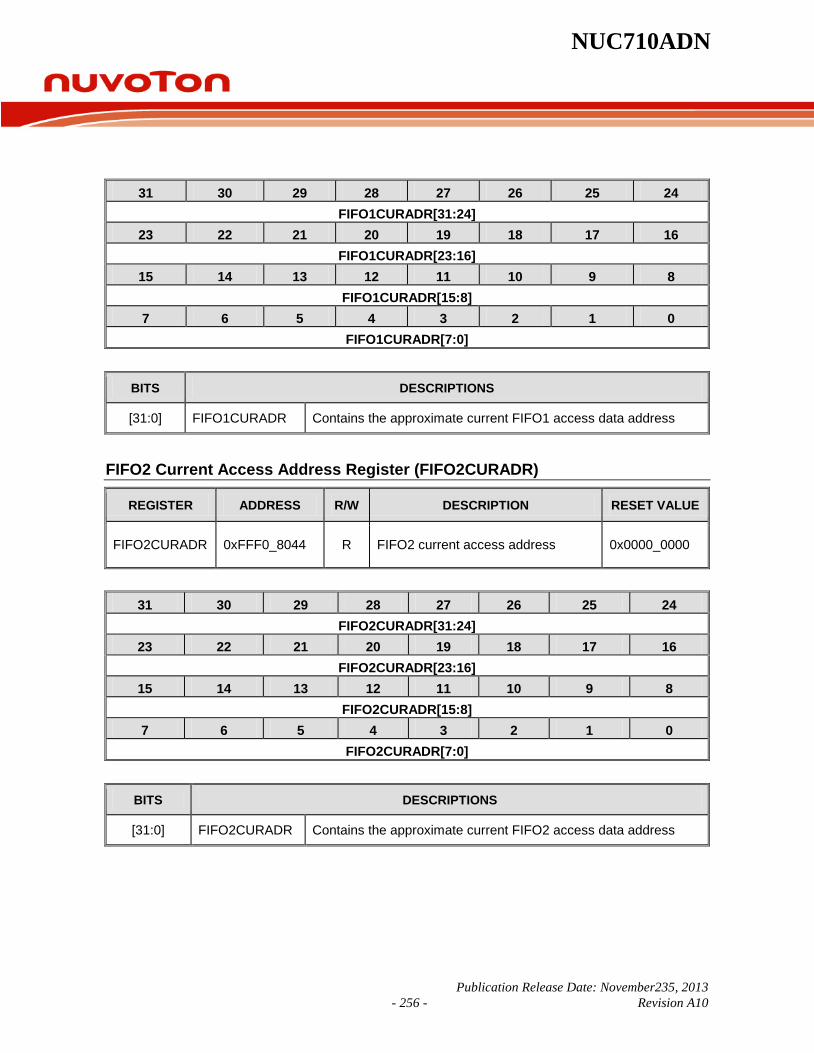
NUC710ADN
Publication Release Date: November235, 2013 - 256 - Revision A10
31 30 29 28 27 26 25 24 FIFO1CURADR[31:24]
23 22 21 20 19 18 17 16 FIFO1CURADR[23:16]
15 14 13 12 11 10 9 8 FIFO1CURADR[15:8]
7 6 5 4 3 2 1 0 FIFO1CURADR[7:0]
BITS DESCRIPTIONS
[31:0] FIFO1CURADR Contains the approximate current FIFO1 access data address
FIFO2 Current Access Address Register (FIFO2CURADR)
REGISTER ADDRESS R/W DESCRIPTION RESET VALUE
FIFO2CURADR 0xFFF0_8044 R FIFO2 current access address 0x0000_0000
31 30 29 28 27 26 25 24 FIFO2CURADR[31:24]
23 22 21 20 19 18 17 16 FIFO2CURADR[23:16]
15 14 13 12 11 10 9 8 FIFO2CURADR[15:8]
7 6 5 4 3 2 1 0 FIFO2CURADR[7:0]
BITS DESCRIPTIONS
[31:0] FIFO2CURADR Contains the approximate current FIFO2 access data address
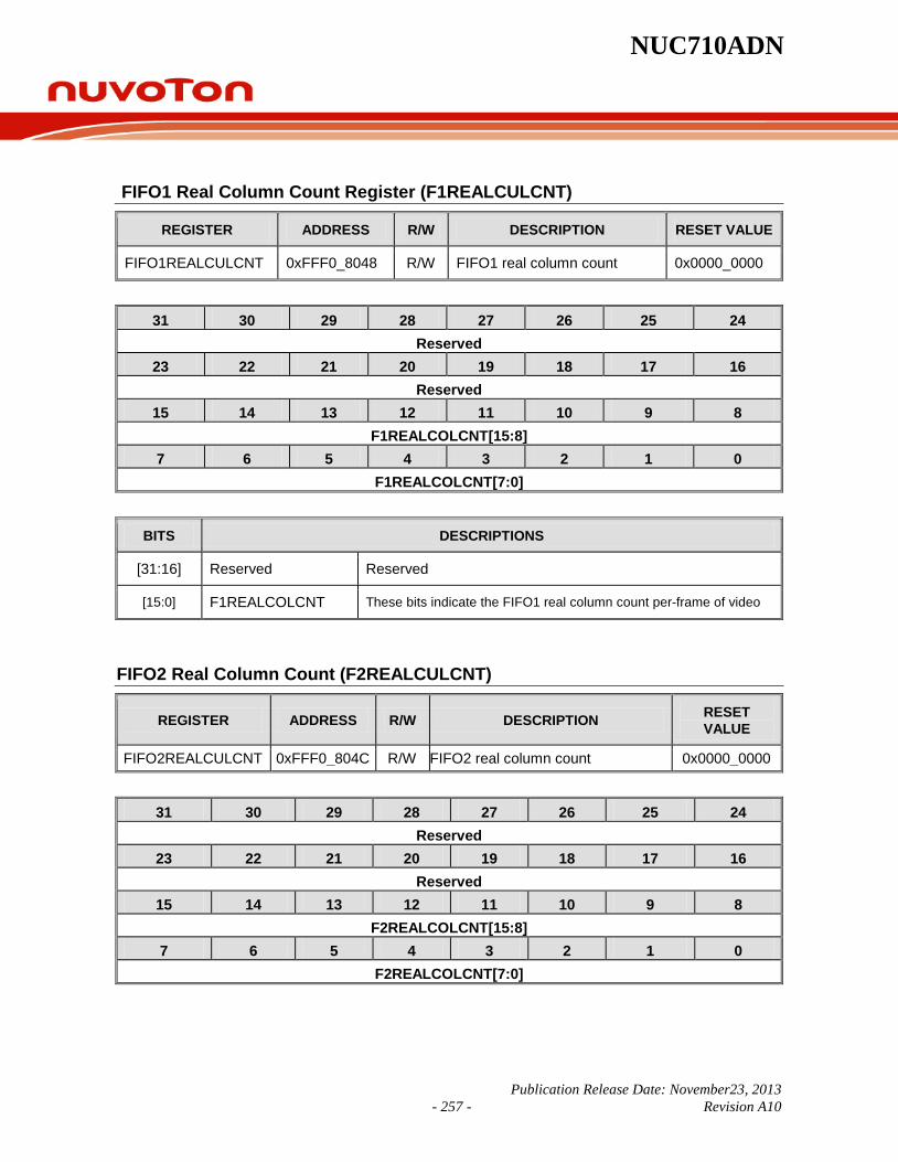
NUC710ADN
Publication Release Date: November23, 2013 - 257 - Revision A10
FIFO1 Real Column Count Register (F1REALCULCNT)
REGISTER ADDRESS R/W DESCRIPTION RESET VALUE
FIFO1REALCULCNT 0xFFF0_8048 R/W FIFO1 real column count 0x0000_0000
31 30 29 28 27 26 25 24 Reserved
23 22 21 20 19 18 17 16 Reserved
15 14 13 12 11 10 9 8 F1REALCOLCNT[15:8]
7 6 5 4 3 2 1 0 F1REALCOLCNT[7:0]
BITS DESCRIPTIONS
[31:16] Reserved Reserved
[15:0] F1REALCOLCNT These bits indicate the FIFO1 real column count per-frame of video
FIFO2 Real Column Count (F2REALCULCNT)
REGISTER ADDRESS R/W DESCRIPTION RESET VALUE
FIFO2REALCULCNT 0xFFF0_804C R/W FIFO2 real column count 0x0000_0000
31 30 29 28 27 26 25 24 Reserved
23 22 21 20 19 18 17 16 Reserved
15 14 13 12 11 10 9 8 F2REALCOLCNT[15:8]
7 6 5 4 3 2 1 0 F2REALCOLCNT[7:0]

NUC710ADN
Publication Release Date: November235, 2013 - 258 - Revision A10
BITS DESCRIPTIONS
[31:16] Reserved Reserved
[15:0] F2REALCOLCNT These bits indicate the FIFO2 real column count per-line of video
24bpp image format:
(BSWP=0, HSWP=0, BPP24SWP=0)
D[31:24] D[23:0]
0000H Dummy Bit Pixel 1
0004H Dummy Bit Pixel 2
0008H Dummy Bit Pixel 3
……….
(BSWP=0, HSWP=0, BPP24SWP=1)
D[31:8] D[7:0]
0000H Pixel 1 Dummy Bit
0004H Pixel 2 Dummy Bit
0008H Pixel 3 Dummy Bit
……….
18bpp image format:
(BSWP=0, HSWP=0, BPP18SWP=0)
D[31:18] D[17:0]
0000H Dummy Bit Pixel 1
0004H Dummy Bit Pixel 2
0008H Dummy Bit Pixel 3
……….

NUC710ADN
Publication Release Date: November23, 2013 - 259 - Revision A10
(BSWP=0, HSWP=0, BPP18SWP=1)
D[31:18] D[17:0]
0000H Pixel 1 Dummy Bit
0004H Pixel 2 Dummy Bit
0008H Pixel 3 Dummy Bit
……….
16bpp image format:
(BSWP=0, HSWP=0)
D[31:16] D[15:0]
0000H Pixel 2 Pixel 1
0004H Pixel 4 Pixel 3
0008H Pixel 6 Pixel 5
……….
(BSWP=0, HSWP=1)
D[31:16] D[15:0]
0000H Pixel 1 Pixel 2
0004H Pixel 3 Pixel 4
0008H Pixel 5 Pixel 6
……….

NUC710ADN
Publication Release Date: November235, 2013 - 260 - Revision A10
12bpp image format: (BSWP=0, HSWP=0)
D[31:28] P[27:16] P[15:12] D[11:0]
0000H Dummy Bit Pixel 2 Dummy Bit Pixel 1
0004H Dummy Bit Pixel 4 Dummy Bit Pixel 3
0008H Dummy Bit Pixel 6 Dummy Bit Pixel 5
……….
(BSWP=0, HSWP=1)
D[31:28] P[27:16] P[15:12] D[11:0]
0000H Dummy Bit Pixel 1 Dummy Bit Pixel 2
0004H Dummy Bit Pixel 3 Dummy Bit Pixel 4
0008H Dummy Bit Pixel 5 Dummy Bit Pixel 6
……….
8bpp image format:
(BSWP=0, HSWP=0)
D[31:24] P[23:16] P[15:8] D[7:0]
0000H Pixel 4 Pixel 3 Pixel 2 Pixel 1
0004H Pixel 8 Pixel 7 Pixel 6 Pixel 5
0008H Pixel 12 Pixel 11 Pixel 10 Pixel 9
……….
(BSWP=1, HSWP=0)
D[31:24] P[23:16] P[15:8] D[7:0]
0000H Pixel 1 Pixel 2 Pixel 3 Pixel 4
0004H Pixel 5 Pixel 6 Pixel 7 Pixel 8
0008H Pixel 9 Pixel 10 Pixel 11 Pixel 12
……….

NUC710ADN
Publication Release Date: November23, 2013 - 261 - Revision A10
4bpp image format: (BSWP=0, HSWP=0)
D[31:28] P[27:24] D[23:20] D[19:16] D[15:12] D[11:8] D[7:4] D[3:0]
0000H Pixel 7 Pixel 8 Pixel 5 Pixel 6 Pixel 3 Pixel 4 Pixel 1 Pixel 2
0004H Pixel 15 Pixel 16 Pixel 13 Pixel 14 Pixel 11 Pixel 12 Pixel 9 Pixel 10
……
(BSWP=1, HSWP=0)
D[31:28] P[27:24] D[23:20] D[19:16] D[15:12] D[11:8] D[7:4] D[3:0]
0000H Pixel 1 Pixel 2 Pixel 3 Pixel 4 Pixel 5 Pixel 6 Pixel 7 Pixel 8
0004H Pixel 9 Pixel 10 Pixel 11 Pixel 12 Pixel 13 Pixel 14 Pixel 15 Pixel 16
….
2bpp image format:
(BSWP=0, HSWP=0)
0000H D[31:30] P[29:28] D[27:26] D[25:24] D[23:22] D[21:20] D[19:18] D[17:16]
Pixel 13 Pixel 14 Pixel 15 Pixel 16 Pixel 9 Pixel 10 Pixel 11 Pixel 12
D[15:14] P[13:12] D[11:10] D[9:8] D[7:6] D[5:4] D[3:2] D[1:0]
Pixel 5 Pixel 6 Pixel 7 Pixel 8 Pixel 1 Pixel 2 Pixel 3 Pixel 4
0004H D[31:30] P[29:28] D[27:26] D[25:24] D[23:22] D[21:20] D[19:18] D[17:16]
Pixel 29 Pixel 30 Pixel 31 Pixel 32 Pixel 25 Pixel 26 Pixel 27 Pixel 28
D[15:14] P[13:12] D[11:10] D[9:8] D[7:6] D[5:4] D[3:2] D[1:0]
Pixel 21 Pixel 22 Pixel 23 Pixel 24 Pixel 17 Pixel 18 Pixel 19 Pixel 20
…….

NUC710ADN
Publication Release Date: November235, 2013 - 262 - Revision A10
(BSWP=1, HSWP=0)
0000H D[31:30] P[29:28] D[27:26] D[25:24] D[23:22] D[21:20] D[19:18] D[17:16]
Pixel 1 Pixel 2 Pixel 3 Pixel 4 Pixel 5 Pixel 6 Pixel 7 Pixel 8
D[15:14] P[13:12] D[11:10] D[9:8] D[7:6] D[5:4] D[3:2] D[1:0]
Pixel 9 Pixel 10 Pixel 11 Pixel 12 Pixel 13 Pixel 14 Pixel 15 Pixel 16
0004H D[31:30] P[29:28] D[27:26] D[25:24] D[23:22] D[21:20] D[19:18] D[17:16]
Pixel 17 Pixel 18 Pixel 19 Pixel 20 Pixel 21 Pixel 22 Pixel 23 Pixel 24
D[15:14] P[13:12] D[11:10] D[9:8] D[7:6] D[5:4] D[3:2] D[1:0]
Pixel 25 Pixel 26 Pixel 27 Pixel 28 Pixel 29 Pixel 30 Pixel 31 Pixel 32
….
1bpp image format:
(BSWP=0, HSWP=0)
0000H D[31] P[30] D[29] D[28] D[27] D[26] D[25] D[24]
Pixel 25 Pixel 26 Pixel 27 Pixel 28 Pixel 29 Pixel 30 Pixel 31 Pixel 32
D[23] P[22] D[21] D[20] D[19] D[18] D[17] D[16]
Pixel 17 Pixel 18 Pixel 19 Pixel 20 Pixel 21 Pixel 22 Pixel 23 Pixel 24
D[15] P[14] D[13] D[12] D[11] D[10] D[9] D[8]
Pixel 9 Pixel 10 Pixel 11 Pixel 12 Pixel 13 Pixel 14 Pixel 15 Pixel 16
D[7] P[6] D[5] D[4] D[3] D[2] D[1] D[0]
Pixel 1 Pixel 2 Pixel 3 Pixel 4 Pixel 5 Pixel 6 Pixel 7 Pixel 8
….

NUC710ADN
Publication Release Date: November23, 2013 - 263 - Revision A10
(BSWP=0, HSWP=0)
0000H D[31] P[30] D[29] D[28] D[27] D[26] D[25] D[24]
Pixel 1 Pixel 2 Pixel 3 Pixel 4 Pixel 5 Pixel 6 Pixel 7 Pixel 8
D[23] P[22] D[21] D[20] D[19] D[18] D[17] D[16]
Pixel 9 Pixel 10 Pixel 11 Pixel 12 Pixel 13 Pixel 14 Pixel 15 Pixel 16
D[15] P[14] D[13] D[12] D[11] D[10] D[9] D[8]
Pixel 17 Pixel 18 Pixel 19 Pixel 20 Pixel 21 Pixel 22 Pixel 23 Pixel 24
D[7] P[6] D[5] D[4] D[3] D[2] D[1] D[0]
Pixel 25 Pixel 26 Pixel 27 Pixel 28 Pixel 29 Pixel 30 Pixel 31 Pixel 32
……….
If there is an image with size 480*480, 24bpp, stored in a memory device with starting address 0x30000000; 24bpp means there are 4 bytes to a pixel (3 bytes containing color, and a dummy byte). So: FIFO1SADDR = 0x30000000 FIFO1COLCNT = 0x01E0 FIFO1ROWCNT = 0x01E0 FIFO1REALCOLCNT = 0x01E0 The unit of FIFOCOLCNT is word. So, if the image is 16bpp, FIFO1COLCNT and FIFO1REALCOLCNT are modified to 0x00F0 because under 16bpp mode, a word contains two data pixels. When FIFO receives the value which FIFOCOLCNT specified, the VLINEFINSH interrupt is generated and
(1) Row counter will increment. When row counter receives the value, which FIFOROWCNT specified, VFRAMFINSH interrupt is generated. So, FIFOROWCNT is not concerned with BPP.
(2) FIFOSTRIDE is load in and added to the current accessed address Column counter counts the FIFO writing pulse. If a Horizontal Upscaling factor is 2X, FIFO will extract a pixel data to two pixel data internal. So if Horizontal Upscaling function is enabled, FIFOCOLCNT need to divided again or VLINEFINSH interrupt is generated after the FIFO has received two columns of data and FIFOROWCNT and VFRAMFINSH interrupt is influenced too. The same with Horizontal Downscaling function, so it’s recommend that Horizontal Downscaling Factor M is a multiple of 4. When VFRAMEFINSH interrupt generated, the FIFO will fetch image data and restart at FIFO1SADDR.

NUC710ADN
Publication Release Date: November235, 2013 - 264 - Revision A10
Fig. 6.10.5.7 FIFO parameter example
If there is an image with size 480*480, 24bpp, stored in the memory device with starting address 0x30000000, and connected with a 480*480 LCD Panel, and the user wants to show the whole image on the LCD Panel, the register settings are: FIFO1SADDR = 0x30000000 FIFO1COLCNT = 0x01E0 FIFO1ROWCNT = 0x01E0 FIFO1REALCOLCNT = 0x01E0 If the LCD Controller is connected with a 240*240 LCD Panel or the user only wants to show a part (red line region, 240*240) of the whole image on a 480*480 LCD Panel, the register settings are: FIFO1SADDR = 0x3001C3E0 (0x30000000 + 4*(480*60+120) = 0x3001C3E0) FIFO1COLCNT = 0x00F0 FIFO1ROWCNT = 0x00F0 FIFOSTRIDE = 0x03C0 (240*4 = 0x03C0) FIFO1REALCOLCNT = 0x00F0 After the register setting is complete, enable FIFO and it will fetch the image data according to the register value. In additionl, if the image in FIFO is smaller than the LCD Panel, DISPWYS, DISPWXS, DISPWYE, DISPWXE must be configured. Usually, FIFO Real Column Count is the same as FIFO Column Count. But if the Horizontal Downscaling function is enabled (factor M is not equal with N), FIFO Real Column Count specifies the column count of the original image, and FIFO Column Count specifies the column count of the scaled image. If there is a picture with N BPP and horizontal width X pixel, the word-count W of this picture is:
480 pixels
480 pixels
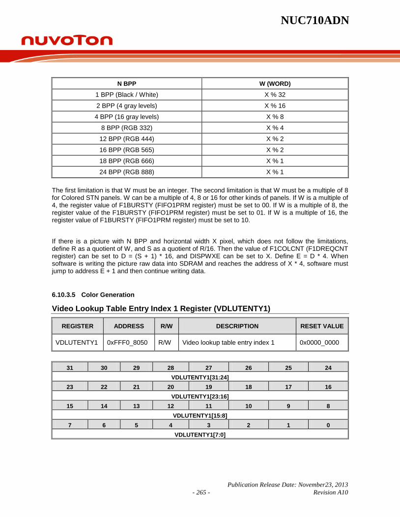
NUC710ADN
Publication Release Date: November23, 2013 - 265 - Revision A10
N BPP W (WORD)
1 BPP (Black / White) X % 32
2 BPP (4 gray levels) X % 16
4 BPP (16 gray levels) X % 8
8 BPP (RGB 332) X % 4
12 BPP (RGB 444) X % 2
16 BPP (RGB 565) X % 2
18 BPP (RGB 666) X % 1
24 BPP (RGB 888) X % 1 The first limitation is that W must be an integer. The second limitation is that W must be a multiple of 8 for Colored STN panels. W can be a multiple of 4, 8 or 16 for other kinds of panels. If W is a multiple of 4, the register value of F1BURSTY (FIFO1PRM register) must be set to 00. If W is a multiple of 8, the register value of the F1BURSTY (FIFO1PRM register) must be set to 01. If W is a multiple of 16, the register value of F1BURSTY (FIFO1PRM register) must be set to 10. If there is a picture with N BPP and horizontal width X pixel, which does not follow the limitations, define R as a quotient of W, and S as a quotient of R/16. Then the value of F1COLCNT (F1DREQCNT register) can be set to D = (S + 1) * 16, and DISPWXE can be set to X. Define E = D * 4. When software is writing the picture raw data into SDRAM and reaches the address of X * 4, software must jump to address E + 1 and then continue writing data.
6.10.3.5 Color Generation
Video Lookup Table Entry Index 1 Register (VDLUTENTY1)
REGISTER ADDRESS R/W DESCRIPTION RESET VALUE
VDLUTENTY1 0xFFF0_8050 R/W Video lookup table entry index 1 0x0000_0000
31 30 29 28 27 26 25 24 VDLUTENTY1[31:24]
23 22 21 20 19 18 17 16 VDLUTENTY1[23:16]
15 14 13 12 11 10 9 8 VDLUTENTY1[15:8]
7 6 5 4 3 2 1 0 VDLUTENTY1[7:0]

NUC710ADN
Publication Release Date: November235, 2013 - 266 - Revision A10
BITS DESCRIPTIONS
[31:0] VDLUTENTY1
Theses bits define address of Lookup Table SRAM when Video pixel data is 00 = VDLUTENTY1[7:0] 01 = VDLUTENTY1[15:8] 10 = VDLUTENTY1[23:16] 11 = VDLUTENTY1[31:24]
Video Lookup Table Entry Index 2 Register (VDLUTENTY2)
REGISTER ADDRESS R/W DESCRIPTION RESET VALUE
VDLUTENTY2 0xFFF0_8054 R/W Video lookup table entry index 2 0x0000_0000
31 30 29 28 27 26 25 24 VDLUTENTY2[31:24]
23 22 21 20 19 18 17 16 VDLUTENTY2[23:16]
15 14 13 12 11 10 9 8 VDLUTENTY2[15:8]
7 6 5 4 3 2 1 0 VDLUTENTY2[7:0]
BITS DESCRIPTIONS
[31:0] VDLUTENTY2
These bits define the address of the SRAM Lookup Table when Video pixel data is 00 = VDLUTENTY2[7:0] 01 = VDLUTENTY2[15:8] 10 = VDLUTENTY2[23:16] 11 = VDLUTENTY2[31:24]
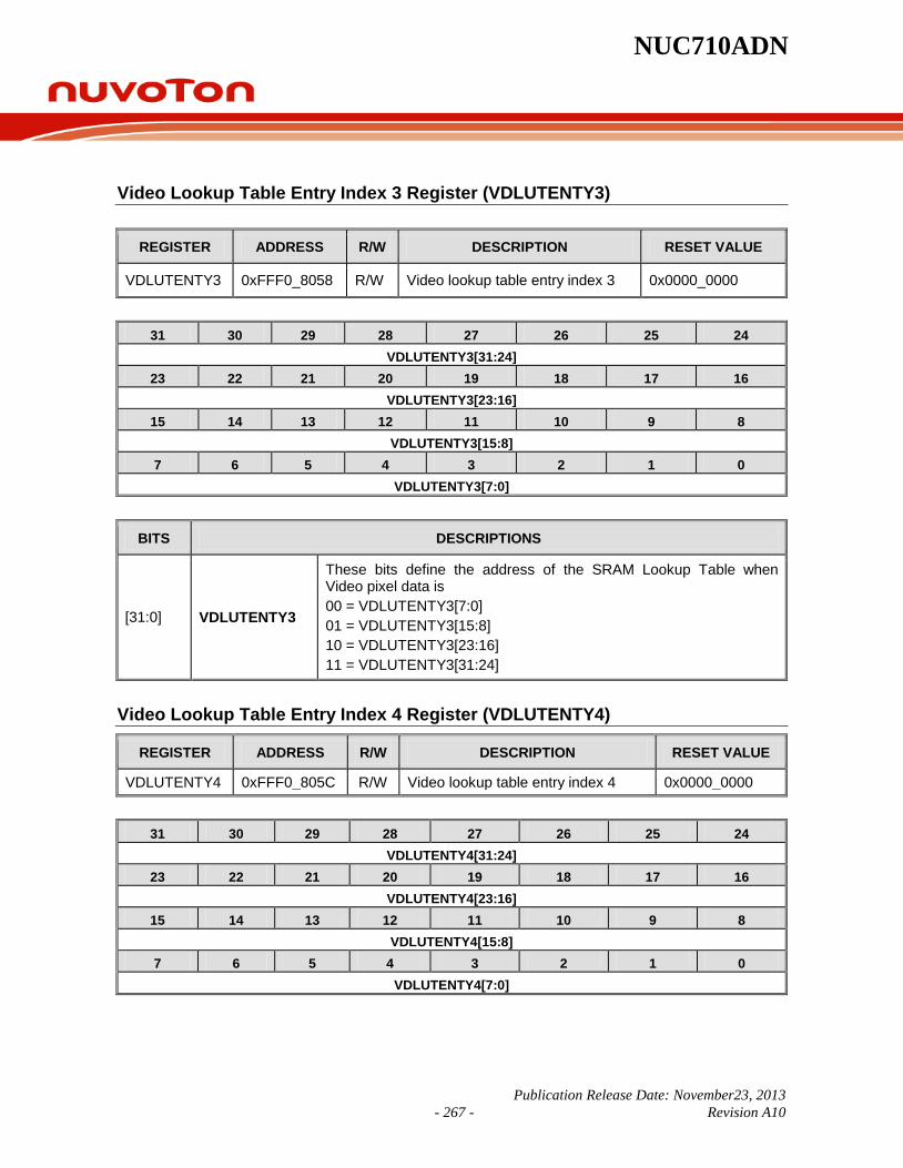
NUC710ADN
Publication Release Date: November23, 2013 - 267 - Revision A10
Video Lookup Table Entry Index 3 Register (VDLUTENTY3)
REGISTER ADDRESS R/W DESCRIPTION RESET VALUE
VDLUTENTY3 0xFFF0_8058 R/W Video lookup table entry index 3 0x0000_0000
31 30 29 28 27 26 25 24 VDLUTENTY3[31:24]
23 22 21 20 19 18 17 16 VDLUTENTY3[23:16]
15 14 13 12 11 10 9 8 VDLUTENTY3[15:8]
7 6 5 4 3 2 1 0 VDLUTENTY3[7:0]
BITS DESCRIPTIONS
[31:0] VDLUTENTY3
These bits define the address of the SRAM Lookup Table when Video pixel data is 00 = VDLUTENTY3[7:0] 01 = VDLUTENTY3[15:8] 10 = VDLUTENTY3[23:16] 11 = VDLUTENTY3[31:24]
Video Lookup Table Entry Index 4 Register (VDLUTENTY4)
REGISTER ADDRESS R/W DESCRIPTION RESET VALUE
VDLUTENTY4 0xFFF0_805C R/W Video lookup table entry index 4 0x0000_0000
31 30 29 28 27 26 25 24 VDLUTENTY4[31:24]
23 22 21 20 19 18 17 16 VDLUTENTY4[23:16]
15 14 13 12 11 10 9 8 VDLUTENTY4[15:8]
7 6 5 4 3 2 1 0 VDLUTENTY4[7:0]
NUC710ADN
Publication Release Date: November235, 2013 - 268 - Revision A10
BITS DESCRIPTIONS
[31:0] VDLUTENTY4
These bits define the address of the SRAM Lookup Table when Video pixel data is 00 = VDLUTENTY4[7:0] 01 = VDLUTENTY4[15:8] 10 = VDLUTENTY4[23:16] 11 = VDLUTENTY4[31:24]
OSD Lookup Table Entry Index 1 Register (OSDLUTENTRY1)
REGISTER ADDRESS R/W DESCRIPTION RESET VALUE
OSDLUTENTRY1 0xFFF0_8060 R/W OSD lookup table entry index 1
0x0000_0000
31 30 29 28 27 26 25 24 OSDLUTENTRY1[31:24]
23 22 21 20 19 18 17 16 OSDLUTENTRY1[23:16]
15 14 13 12 11 10 9 8 OSDLUTENTRY1[15:8]
7 6 5 4 3 2 1 0 OSDLUTENTRY1[7:0]
BITS DESCRIPTIONS
[31:0] OSDLUTENTRY1
These bits define the address of the SRAM Lookup Table when OSD pixel data is 00 = OSDLUTENTRY1[7:0] 01 = OSDLUTENTRY1[15:8] 10 = OSDLUTENTRY1[23:16] 11 = OSDLUTENTRY1[31:24]

NUC710ADN
Publication Release Date: November23, 2013 - 269 - Revision A10
OSD Lookup Table Entry Index 2 Register (OSDLUTENTRY2)
REGISTER ADDRESS R/W DESCRIPTION RESET VALUE
OSDLUTENTRY2 0xFFF0_8064 R/W OSD lookup table entry index 2 0x0000_0000
31 30 29 28 27 26 25 24 OSDLUTENTRY2[31:24]
23 22 21 20 19 18 17 16 OSDLUTENTRY2[23:16]
15 14 13 12 11 10 9 8 OSDLUTENTRY2[15:8]
7 6 5 4 3 2 1 0 OSDLUTENTRY2[7:0]
BITS DESCRIPTIONS
[31:0] OSDLUTENTRY2
These bits define the address of the SRAM Lookup Table when OSD pixel data is 00 = OSDLUTENTRY2[7:0] 01 = OSDLUTENTRY2[15:8] 10 = OSDLUTENTRY2[23:16] 11 = OSDLUTENTRY2[31:24]
OSD Lookup Table Entry Index 3 Register (OSDLUTENTRY3)
REGISTER ADDRESS R/W DESCRIPTION RESET VALUE
OSDLUTENTRY3 0xFFF0_8068 R/W OSD lookup table entry index 3 0x0000_0000
31 30 29 28 27 26 25 24 OSDLUTENTRY3[31:24]
23 22 21 20 19 18 17 16 OSDLUTENTRY3[23:16]
15 14 13 12 11 10 9 8 OSDLUTENTRY3[15:8]
7 6 5 4 3 2 1 0 OSDLUTENTRY3[7:0]
NUC710ADN
Publication Release Date: November235, 2013 - 270 - Revision A10
BITS DESCRIPTIONS
[31:0] OSDLUTENTRY3
These bits define the address of the SRAM Lookup Table when OSD pixel data is 00 = OSDLUTENTRY3[7:0] 01 = OSDLUTENTRY3[15:8] 10 = OSDLUTENTRY3[23:16] 11 = OSDLUTENTRY3[31:24]
OSD Lookup Table Entry Index 4 Register (OSDLUTENTRY4)
REGISTER ADDRESS R/W DESCRIPTION RESET VALUE
OSDLUTENTRY4 0xFFF0_806C R/W OSD lookup table entry index 4 0x0000_0000
31 30 29 28 27 26 25 24 OSDLUTENTRY4[31:24]
23 22 21 20 19 18 17 16 OSDLUTENTRY4[23:16]
15 14 13 12 11 10 9 8 OSDLUTENTRY4[15:8]
7 6 5 4 3 2 1 0 OSDLUTENTRY4[7:0]
BITS DESCRIPTIONS
[31:0] OSDLUTENTRY4
These bits define the address of the SRAM Lookup Table when OSD pixel data is 00 = OSDLUTENTRY4[7:0] 01 = OSDLUTENTRY4[15:8] 10 = OSDLUTENTRY4[23:16] 11 = OSDLUTENTRY4[31:24]
Dithering Pattern 1 Register (DITHP1)
REGISTER ADDRESS R/W DESCRIPTION RESET VALUE
DITHP1 0xFFF0_8070 R/W Gray level dithered data duty pattern 1 0x0101_0001
NUC710ADN
Publication Release Date: November23, 2013 - 271 - Revision A10
31 30 29 28 27 26 25 24 DP2[15:8]
23 22 21 20 19 18 17 16 DP2[7:0]
15 14 13 12 11 10 9 8 DP1[15:8]
7 6 5 4 3 2 1 0 DP1[7:0]
BITS DESCRIPTIONS
[31:16] DP2 Recommended pattern value for “4’b0010” gray level 0000 0001 0000 0001
[15:0] DP1 Recommended pattern value for “4’b0001” gray level 0000 0000 0000 0001
Dithering Pattern 2 Register (DITHP2)
REGISTER ADDRESS R/W DESCRIPTION RESET VALUE
DITHP2 0xFFF0_8074 R/W Gray level dithered data duty pattern 2 0x1111_0841
31 30 29 28 27 26 25 24 DP4[15:8]
23 22 21 20 19 18 17 16 DP4[7:0]
15 14 13 12 11 10 9 8 DP3[15:8]
7 6 5 4 3 2 1 0 DP3[7:0]
BITS DESCRIPTIONS
[31:16] DP4 Recommended pattern value for “4’b0100” gray level 0001 0001 0001 0001
[15:0] DP3 Recommended pattern value for “4’b0011” gray level 0000 1000 0100 0001
Dithering Pattern 3 Register (DITHP3)

NUC710ADN
Publication Release Date: November235, 2013 - 272 - Revision A10
REGISTER ADDRESS R/W DESCRIPTION RESET VALUE
DITHP3 0xFFF0_8078 R/W Gray level dithered data duty pattern 3 0x4949_2491
31 30 29 28 27 26 25 24 DP6[15:8]
23 22 21 20 19 18 17 16 DP6[7:0]
15 14 13 12 11 10 9 8 DP5[15:8]
7 6 5 4 3 2 1 0 DP5[7:0]
BITS DESCRIPTIONS
[31:16] DP6 Recommended pattern value “4’’b0110” gray level 0100 1001 0100 1001
[15:0] DP5 Recommended pattern value “4’’b0101” gray level 0010 0100 1001 0001
Dithering Pattern 4 Register (DITHP4)
REGISTER ADDRESS R/W DESCRIPTION RESET VALUE
DITHP4 0xFFF0_807C R/W Gray level dithered data duty pattern 4 0x5555_52A5
31 30 29 28 27 26 25 24 DP8[15:8]
23 22 21 20 19 18 17 16 DP8[7:0]
15 14 13 12 11 10 9 8 DP7[15:8]
7 6 5 4 3 2 1 0 DP7[7:0]

NUC710ADN
Publication Release Date: November23, 2013 - 273 - Revision A10
BITS DESCRIPTIONS
[31:16] DP8 Recommended pattern value “4’’b1000” gray level 0101 0101 0101 0101
[15:0] DP7 Recommended pattern value “4’’b0111” gray level 0101 0010 1010 1001
Dithering Pattern 5 Register (DITHP5)
REGISTER ADDRESS R/W DESCRIPTION RESET VALUE
DITHP5 0xFFF0_8080 R/W Gray level dithered data duty pattern 5 0xB6B6_B556
31 30 29 28 27 26 25 24 DP10[15:8]
23 22 21 20 19 18 17 16 DP10[7:0]
15 14 13 12 11 10 9 8 DP9[15:8]
7 6 5 4 3 2 1 0 DP9[7:0]
BITS DESCRIPTIONS
[31:16] DP10 Recommended pattern value “4’’b1010” gray level 1011 0110 1011 0110
[15:0] DP9 Recommended pattern value “4’’b1001” gray level 1011 0101 0101 0110
Dithering Pattern 6 Register (DITHP6)
REGISTER ADDRESS R/W DESCRIPTION RESET VALUE
DITHP6 0xFFF0_8084 R/W Gray level dithered data duty pattern 6 0xEEEE_DB6E

NUC710ADN
Publication Release Date: November235, 2013 - 274 - Revision A10
31 30 29 28 27 26 25 24 DP12[15:8]
23 22 21 20 19 18 17 16 DP12[7:0]
15 14 13 12 11 10 9 8 DP11[15:8]
7 6 5 4 3 2 1 0 DP11[7:0]
BITS DESCRIPTIONS
[31:16] DP12 Recommended pattern value “4’’b1100” gray level 1110 1110 1110 1110
[15:0] DP11 Recommended pattern value “4’’b1011” gray level 1101 1011 0110 1110
Dithering Pattern 7 Register (DITHP7)
REGISTER ADDRESS R/W DESCRIPTION RESET VALUE
DITHP7 0xFFF0_8088 R/W Gray level dithered data duty pattern 7 0xFEFE_EFBE
31 30 29 28 27 26 25 24 DP14[15:8]
23 22 21 20 19 18 17 16 DP14[7:0]
15 14 13 12 11 10 9 8 DP13[15:8]
7 6 5 4 3 2 1 0 DP13[7:0]
BITS DESCRIPTIONS
[31:16] DP14 Recommended pattern value “4’’b1110” gray level 1111 1110 1111 1110
[15:0] DP13 Recommended pattern value “4’’b1101” gray level 1110 1111 1011 1110
The 4bpp flow is the same with 2bpp.
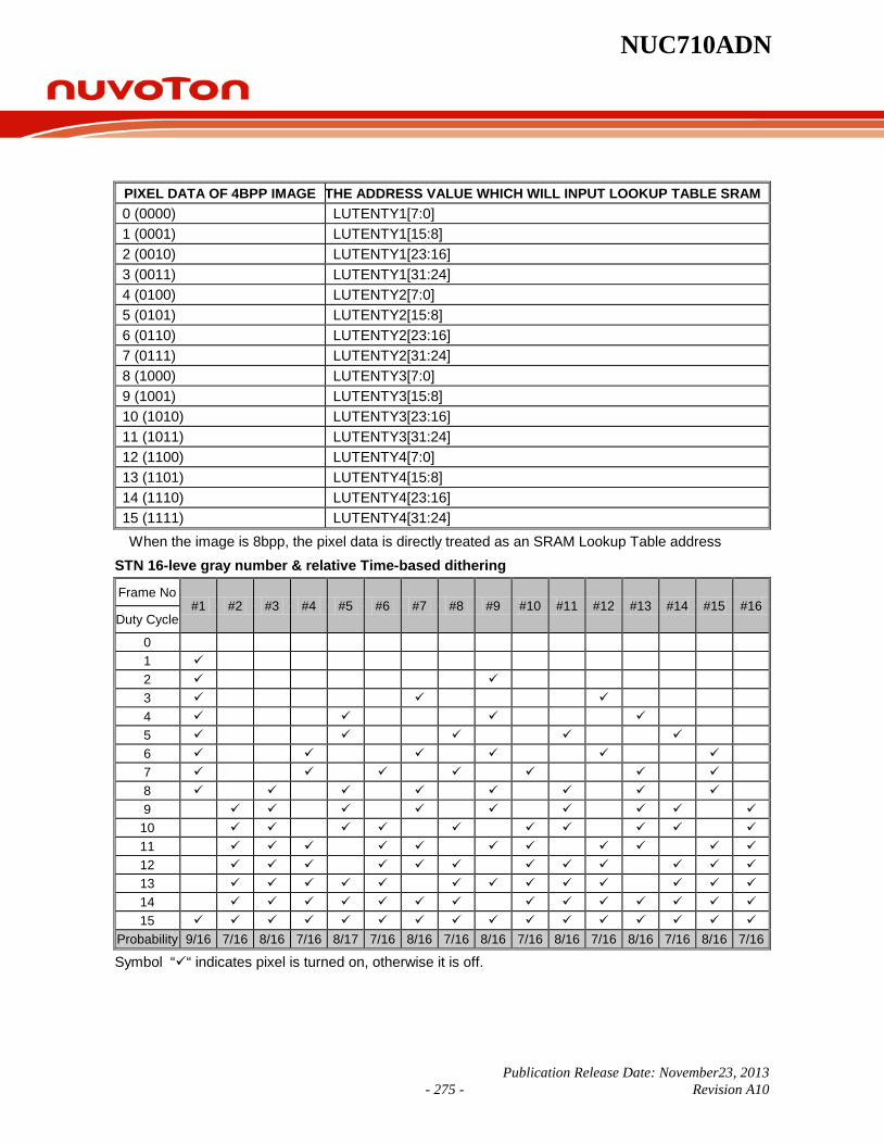
NUC710ADN
Publication Release Date: November23, 2013 - 275 - Revision A10
PIXEL DATA OF 4BPP IMAGE THE ADDRESS VALUE WHICH WILL INPUT LOOKUP TABLE SRAM 0 (0000) LUTENTY1[7:0] 1 (0001) LUTENTY1[15:8] 2 (0010) LUTENTY1[23:16] 3 (0011) LUTENTY1[31:24] 4 (0100) LUTENTY2[7:0] 5 (0101) LUTENTY2[15:8] 6 (0110) LUTENTY2[23:16] 7 (0111) LUTENTY2[31:24] 8 (1000) LUTENTY3[7:0] 9 (1001) LUTENTY3[15:8] 10 (1010) LUTENTY3[23:16] 11 (1011) LUTENTY3[31:24] 12 (1100) LUTENTY4[7:0] 13 (1101) LUTENTY4[15:8] 14 (1110) LUTENTY4[23:16] 15 (1111) LUTENTY4[31:24] When the image is 8bpp, the pixel data is directly treated as an SRAM Lookup Table address
STN 16-leve gray number & relative Time-based dithering
Frame No #1 #2 #3 #4 #5 #6 #7 #8 #9 #10 #11 #12 #13 #14 #15 #16
Duty Cycle
0 1 2 3 4 5 6 7 8 9
10 11 12 13 14 15
Probability 9/16 7/16 8/16 7/16 8/17 7/16 8/16 7/16 8/16 7/16 8/16 7/16 8/16 7/16 8/16 7/16
Symbol ““ indicates pixel is turned on, otherwise it is off.

NUC710ADN
Publication Release Date: November235, 2013 - 276 - Revision A10
6.10.3.6 LCD Post-processing
Dummy Display Color Pattern Register (DDISPCP)
REGISTER ADDRESS R/W DESCRIPTION RESET VALUE
DDISPCP 0xFFF0_8090 R/W Dummy Display Color Pattern 0x0000_0000
31 30 29 28 27 26 25 24 Reserved GRAY
23 22 21 20 19 18 17 16 DDISPR
15 14 13 12 11 10 9 8 DDISPG
7 6 5 4 3 2 1 0 DDISPB
BITS DESCRIPTIONS
[31] Reserved Reserved
[30:24] GRAY Replenish bit for 8bpp when LUTEN is disable
[23:16] DDISPR LCD dummy display data of R component
[15:8] DDISPG LCD dummy display data of G component
[7:0] DDISPB LCD dummy display data of B component
Video Windows Starting Coordinate Register (VWINS)
REGISTER ADDRESS R/W DESCRIPTION RESET VALUE
VWINS 0xFFF0_8094 R/W Video Window Starting Coordinate 0x0000_0000
31 30 29 28 27 26 25 24 VWYS[31:24]
23 22 21 20 19 18 17 16 VWYS[23:16]
15 14 13 12 11 10 9 8 VWXS[15:8]
7 6 5 4 3 2 1 0 VWXS[7:0]

NUC710ADN
Publication Release Date: November23, 2013 - 277 - Revision A10
BITS DESCRIPTIONS
[31:16] VWYS Video Window Y-Start A 16-bit value specifies the vertical starting pixel positions of the LCD display window.
[15:0] VWXS Video Window X-Start A 16-bit value specifies the horizontal starting pixel positions of the LCD display window.
Video Windows Ending Coordinate Register (VWINE)
REGISTER ADDRESS R/W DESCRIPTION RESET VALUE
VWINE 0xFFF0_8098 R/W Video Window Ending Coordinates 0x0000_0000
31 30 29 28 27 26 25 24
VWYE[31:24] 23 22 21 20 19 18 17 16
VWYE[23:16] 15 14 13 12 11 10 9 8
VWXE[15:8] 7 6 5 4 3 2 1 0
VWXE[7:0]
BITS DESCRIPTIONS
[31:16] VWYE Video Window Y-End A 16-bit value specifies the vertical last pixel positions of the LCD display window.
[15:0] VWXE Video Window X-End A 16-bit value specifies the horizontal last pixel positions of the LCD display window.
OSD Windows Starting Coordinate Register (OSDWINS)
REGISTER ADDRESS R/W DESCRIPTION RESET VALUE
OSDWINS 0xFFF0_809C R/W OSD Window Starting Coordinates 0x0000_0000

NUC710ADN
Publication Release Date: November235, 2013 - 278 - Revision A10
31 30 29 28 27 26 25 24 OSDWYS[15:8]
23 22 21 20 19 18 17 16 OSDWYS[7:0]
15 14 13 12 11 10 9 8 OSDWXS[15:8]
7 6 5 4 3 2 1 0 OSDWXS[7:0]
BITS DESCRIPTIONS
[31:16] OSDWYS OSD Window Y-Start A 16-bit value specifies the vertical starting pixel positions of the OSD window.
[15:0] OSDWXS OSD Window X-Start A 16-bit value specifies the horizontal starting pixel positions of the OSD window.
OSD Windows Ending Coordinate Register (OSDWINE)
REGISTER ADDRESS R/W DESCRIPTION RESET VALUE
OSDWINE 0xFFF0_80A0 R/W OSD Window Ending Coordinates 0x0000_0000
31 30 29 28 27 26 25 24 OSDWYE[15:8]
23 22 21 20 19 18 17 16 OSDWYE[7:0]
15 14 13 12 11 10 9 8 OSDWXE[15:8]
7 6 5 4 3 2 1 0 OSDWXE[7:0]
BITS DESCRIPTIONS
[31:16] OSDWYE OSD Window Y-End A 16-bit value specifies the vertical last pixel positions of the OSD window.
[15:0] OSDWXE OSD Window X-End A 16-bit value specifies the horizontal last pixel positions of the OSD window.
OSD Overlay Control Register (OSDOVCN)

NUC710ADN
Publication Release Date: November23, 2013 - 279 - Revision A10
REGISTER ADDRESS R/W DESCRIPTION RESET VALUE
OSDOVCN 0xFFF0_80A4 R/W OSD Overlay Control 0x0000_0000
31 30 29 28 27 26 25 24 Reserved
23 22 21 20 19 18 17 16 BLICNT
15 14 13 12 11 10 9 8 Reserved OSDBLI OSDCKY
7 6 5 4 3 2 1 0 Reserved VASYNW OCR1 OCR0
BITS DESCRIPTIONS
[31:24] Reserved Reserved
[23:16] BLICNT OSD Blinking Cycle Time An 8-bit value specifies the OSD blinking cycle time (unit: Vsync)
[15:10] Reserved Reserved
[9] OSDBLI OSD Blinking Control 0 = Disable 1 = Enable
[8] OSDCKY OSD Color Key Control 0 = Disable 1 = Enable
[7] Reserved Reserved
[6:4] VASYNW Video Synthesis Weight Synthesized video= [Video x VASYNW+ OSD x (8-VASYNW)]/8
[3:2] OCR1
Video/OSD overlay control 1 When display region with OSD window, color-key condition match 00 = Display video data 01 = Display OSD data 10 = Display synthesized (Video+OSD) data

NUC710ADN
Publication Release Date: November235, 2013 - 280 - Revision A10
Continued
BITS DESCRIPTIONS
[1:0] OCR0
Video/OSD overlay control 0 When display region with OSD window, color-key condition un-match 00 = Display video data 01 = Display OSD data 10 = Display synthesized (Video+OSD) data
OSD Overlay Color Key Pattern Register (OSDOVCKP)
REGISTER ADDRESS R/W DESCRIPTION RESET VALUE
OSDOVCKP 0xFFF0_80A8 R/W OSD Overlay Color-Key Pattern 0x0000_0000
31 30 29 28 27 26 25 24 Reserved
23 22 21 20 19 18 17 16 OSDRKYP
15 14 13 12 11 10 9 8 OSDGKYP
7 6 5 4 3 2 1 0 OSDBKYP
BITS DESCRIPTIONS
[31:24] Reserved Reserved
[23:16] OSDRKYP OSD data comparing R component according to the source color format
[15:8] OSDGKYP OSD data comparing G component according to the source color format
[7:0] OSDBKYP OSD data comparing B component according to the source color format
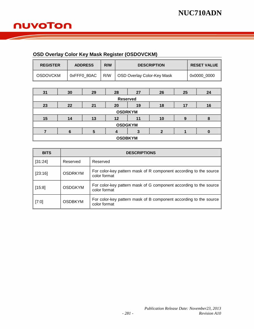
NUC710ADN
Publication Release Date: November23, 2013 - 281 - Revision A10
OSD Overlay Color Key Mask Register (OSDOVCKM)
REGISTER ADDRESS R/W DESCRIPTION RESET VALUE
OSDOVCKM 0xFFF0_80AC R/W OSD Overlay Color-Key Mask 0x0000_0000
31 30 29 28 27 26 25 24 Reserved
23 22 21 20 19 18 17 16 OSDRKYM
15 14 13 12 11 10 9 8 OSDGKYM
7 6 5 4 3 2 1 0 OSDBKYM
BITS DESCRIPTIONS
[31:24] Reserved Reserved
[23:16] OSDRKYM For color-key pattern mask of R component according to the source color format
[15:8] OSDGKYM For color-key pattern mask of G component according to the source color format
[7:0] OSDBKYM For color-key pattern mask of B component according to the source color format
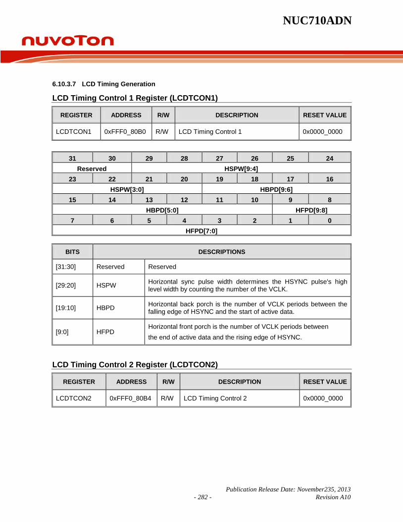
NUC710ADN
Publication Release Date: November235, 2013 - 282 - Revision A10
6.10.3.7 LCD Timing Generation
LCD Timing Control 1 Register (LCDTCON1)
REGISTER ADDRESS R/W DESCRIPTION RESET VALUE
LCDTCON1 0xFFF0_80B0 R/W LCD Timing Control 1 0x0000_0000
31 30 29 28 27 26 25 24 Reserved HSPW[9:4]
23 22 21 20 19 18 17 16 HSPW[3:0] HBPD[9:6]
15 14 13 12 11 10 9 8 HBPD[5:0] HFPD[9:8]
7 6 5 4 3 2 1 0 HFPD[7:0]
BITS DESCRIPTIONS
[31:30] Reserved Reserved
[29:20] HSPW Horizontal sync pulse width determines the HSYNC pulse's high level width by counting the number of the VCLK.
[19:10] HBPD Horizontal back porch is the number of VCLK periods between the falling edge of HSYNC and the start of active data.
[9:0] HFPD Horizontal front porch is the number of VCLK periods between the end of active data and the rising edge of HSYNC.
LCD Timing Control 2 Register (LCDTCON2)
REGISTER ADDRESS R/W DESCRIPTION RESET VALUE
LCDTCON2 0xFFF0_80B4 R/W LCD Timing Control 2 0x0000_0000
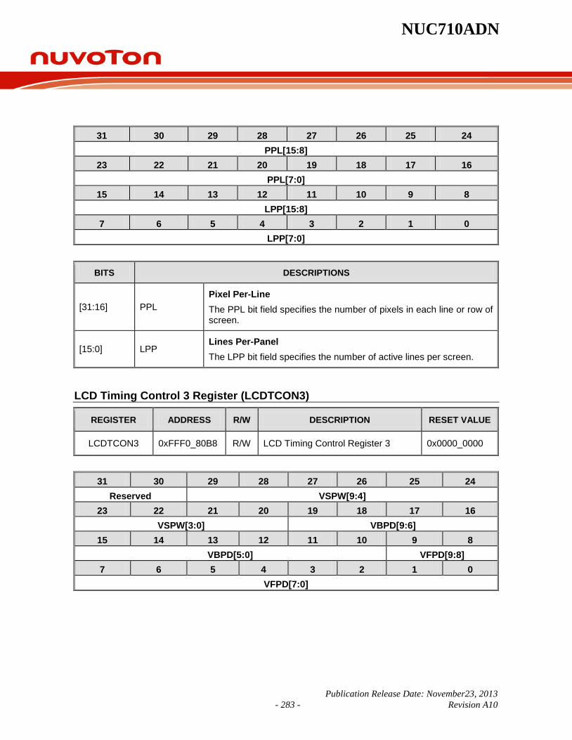
NUC710ADN
Publication Release Date: November23, 2013 - 283 - Revision A10
31 30 29 28 27 26 25 24 PPL[15:8]
23 22 21 20 19 18 17 16 PPL[7:0]
15 14 13 12 11 10 9 8 LPP[15:8]
7 6 5 4 3 2 1 0 LPP[7:0]
BITS DESCRIPTIONS
[31:16] PPL Pixel Per-Line The PPL bit field specifies the number of pixels in each line or row of screen.
[15:0] LPP Lines Per-Panel The LPP bit field specifies the number of active lines per screen.
LCD Timing Control 3 Register (LCDTCON3)
REGISTER ADDRESS R/W DESCRIPTION RESET VALUE
LCDTCON3 0xFFF0_80B8 R/W LCD Timing Control Register 3 0x0000_0000
31 30 29 28 27 26 25 24 Reserved VSPW[9:4]
23 22 21 20 19 18 17 16 VSPW[3:0] VBPD[9:6]
15 14 13 12 11 10 9 8 VBPD[5:0] VFPD[9:8]
7 6 5 4 3 2 1 0 VFPD[7:0]
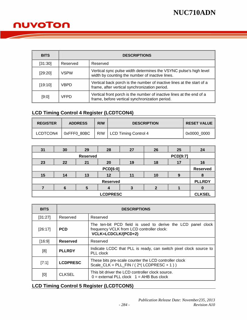
NUC710ADN
Publication Release Date: November235, 2013 - 284 - Revision A10
BITS DESCRIPTIONS
[31:30] Reserved Reserved
[29:20] VSPW Vertical sync pulse width determines the VSYNC pulse's high level width by counting the number of inactive lines.
[19:10] VBPD Vertical back porch is the number of inactive lines at the start of a frame, after vertical synchronization period.
[9:0] VFPD Vertical front porch is the number of inactive lines at the end of a frame, before vertical synchronization period.
LCD Timing Control 4 Register (LCDTCON4)
REGISTER ADDRESS R/W DESCRIPTION RESET VALUE
LCDTCON4 0xFFF0_80BC R/W LCD Timing Control 4 0x0000_0000
31 30 29 28 27 26 25 24 Reserved PCD[9:7]
23 22 21 20 19 18 17 16 PCD[6:0] Reserved
15 14 13 12 11 10 9 8 Reserved PLLRDY
7 6 5 4 3 2 1 0 LCDPRESC CLKSEL
BITS DESCRIPTIONS
[31:27] Reserved Reserved
[26:17] PCD The ten-bit PCD field is used to derive the LCD panel clock frequency VCLK from LCD controller clock: VCLK=LCDCLK/(PCD+2)
[16:9] Reserved Reserved
[8] PLLRDY Indicate LCDC that PLL is ready, can switch pixel clock source to PLL clock
[7:1] LCDPRESC These bits pre-scale counter the LCD controller clock Scale_CLK = PLL_FIN / ( 2*( LCDPRESC + 1 ) )
[0] CLKSEL This bit driver the LCD controller clock source. 0 = external PLL clock 1 = AHB Bus clock
LCD Timing Control 5 Register (LCDTCON5)

NUC710ADN
Publication Release Date: November23, 2013 - 285 - Revision A10
REGISTER ADDRESS R/W DESCRIPTION RESET VALUE
LCDTCON5 0xFFF0_80C0 R/W LCD Timing Control 5 0x0000_0000
31 30 29 28 27 26 25 24 Reserved
23 22 21 20 19 18 17 16 Reserved ACBF
15 14 13 12 11 10 9 8 Reserved
7 6 5 4 3 2 1 0 Reserved MMODE INVVCLK INVHSYN INVVSYN INVVDEN
BITS DESCRIPTIONS
[31:21] Reserved Reserved
[20:16] ACBF Determine the toggle rate of the VDEN AC bias pin). The AC bias pin frequency is only applicable to STN display. Program this field with the number of line clocks between each toggle.
[15:5] Reserved Reserved
[4] MMODE Determine the toggle rate of the VDEN 0 = Each Frame 1 = The rate defined by the ACBF.
[3] INVVCLK This bit controls the polarity of the VCLK active edge. 0 = Panel signal is transit at VCLK rising edge 1 = Panel signal is transit at VCLK falling edge
[2] INVHSYNC This bit indicates the HSYNC pulse polarity. 0 = Normal 1 = Inverted
[1] INVVSYNC This bit indicates the VSYNC pulse polarity. 0 = Normal 1 = Inverted
[0] INVVDEN This bit indicates the VDEN signal polarity. 0 = Normal 1 = Inverted

NUC710ADN
Publication Release Date: November235, 2013 - 286 - Revision A10
LCD Timing Control 6 Register (LCDTCON6)
REGISTER ADDRESS R/W DESCRIPTION RESET VALUE
LCDTCON6 0xFFF0_80C4 R LCD Timing Control 6 0x0000_0000
31 30 29 28 27 26 25 24 PPLCURENT[15:8]
23 22 21 20 19 18 17 16 PPLCURENT[7:0]
15 14 13 12 11 10 9 8 LPPCURENT[15:8]
7 6 5 4 3 2 1 0 LPPCURENT[7;0]
BITS DESCRIPTIONS
[31:16] PPLCURENT Pixel number which LCD Controller is outputting to LCD Panel
[15:0] LPPCURENT Line number which LCD Controller is outputting to LCD Panel
Fig. 6.10.3.7.1 TFT Horizontal display timing diagram
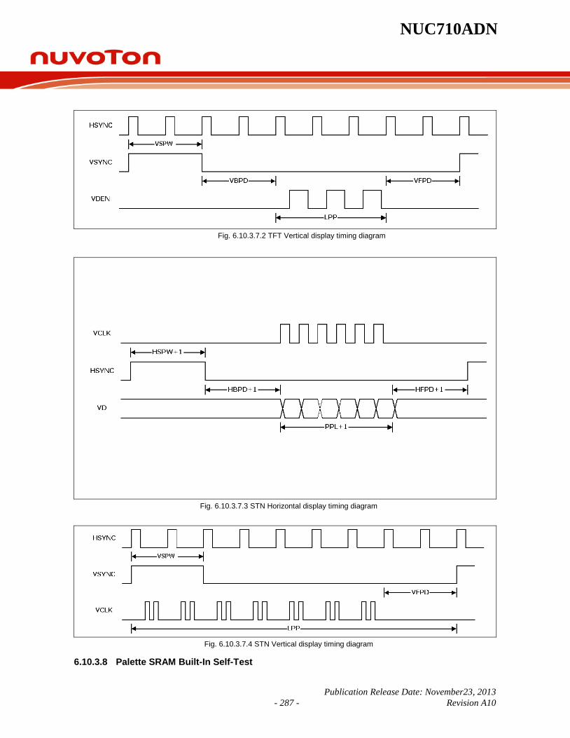
NUC710ADN
Publication Release Date: November23, 2013 - 287 - Revision A10
Fig. 6.10.3.7.2 TFT Vertical display timing diagram
Fig. 6.10.3.7.3 STN Horizontal display timing diagram
Fig. 6.10.3.7.4 STN Vertical display timing diagram
6.10.3.8 Palette SRAM Built-In Self-Test

NUC710ADN
Publication Release Date: November235, 2013 - 288 - Revision A10
Lookup Table SRAM Built-In Self Test Register (BIST)
REGISTER ADDRESS R/W DESCRIPTION RESET VALUE
BIST 0xFFF0_80D0 R/W Lookup Table SRAM Build In Self Test 0x0000_0000
31 30 29 28 27 26 25 24 Reserved
23 22 21 20 19 18 17 16 Reserved
15 14 13 12 11 10 9 8 Reserved
7 6 5 4 3 2 1 0 Reserved FAIL FINISH BISTEN
BITS DESCRIPTIONS
[31:3] Reserved Reserved
[2] FAIL BIST Fail indicator 0 = SRAM BIST not fail 1 = SRAM BIST fail
[1] FINISH
BIST Finish Status (Read Only) 0 = When BIST enabled, this value means BIST not finished 1 = When BIST enabled, this value means BIST finished, and FAIL can be referenced
[0] BISTEN BIST Mode Enable 0 = SRAM is in normal operation. 1 = BIST enabled, SRAM is under BIST test
NUC710ADN
Publication Release Date: November23, 2013 - 289 - Revision A10
6.11 Audio Controller The audio controller consists of IIS/AC-link protocol to interface with external audio CODEC. One 8-level deep FIFO for read path and write path and each level has 32-bit width (16 bits for the right channel and 16 bits for the left channel). One DMA controller handles the data movement between FIFO and memory. The following are the properties of DMA.
• Always 8-beat incrementing burst
• Locks the bus during 8-beat incrementing burst
• When reaching the middle and end address of the destination address, a DMA_IRQ is automatically requested for the CPU
An AHB master port and an AHB slave port are available in the audio controller.
6.11.1 IIS Interface The IIS interface signals are shown as figure 6.11.2.1
Figure 6.11.2.1 The interface signal of IIS
The 16 bits IIS and MSB-justified format are supported, the timing diagram is shown as Figure 6.11.2.2
Audio Controller
Audio Codec
MCLK
BCLK
LRCLK
DOUT
DIN
NUC710ADN
Publication Release Date: November235, 2013 - 290 - Revision A10
LRCLK
BCK
DATA
Left Right
1 2 3
MSB B2
1 2
LSB MSB
I2S bus
LRCLK
BCK
DATA
Left Right
1 2 3
B2 B3
1 2
MSB B2
MSB –Justified format
MSB LSB
Figure 6.11.2.2 The format of IIS
The sampling rate and bit shift clock frequency can be set by the control register ACTL_IISCON.
6.11.2 AC97 Interface The AC97 interface, called AC-link is supported. For input and output direction, each frame contains a Tag slot and 12 data slots. However, in the 12 data slots, only 4 slots are used in NUC710, other 8 slots are not supported, and the control data and audio data are transferred into 4 valid slots. Each slot contains 20 data bits. The interface signals are shown as Figure 6.11.2.1
Figure 6.11.2.1 The AC-link interface signal
Audio Controller
Audio Codec
SYNC
BCLK
DIN
DOUT
RESETB

NUC710ADN
Publication Release Date: November23, 2013 - 291 - Revision A10
The signal format is shown as Figure 6.11.2.2
Figure 6.11.2.2 The AC-link signal format
The output frame structure is shown as below:
SLOT # 0 1 2 3 4 5 6 7 8 9 10 11 12
CONTENT Tag CMD ADDR
CMD DATA
PCM LEFT
PCM RIGHT Unused
BITS 15-0 19-0 19-0 19-0 19-0 159 - 0
PHASE Tag phase Data phase
The output frame data format is shown as follows:
SLOT # BIT DESCRIPTION
Tag (slot 0)
15 Frame validity bit; 1 is valid, 0 is invalid.
14 - 3 Slot validity, but in NUC710, only bits 6-3 are used, bits 14-7 are unused. Bit 3 corresponds to slot 1, bit 4 corresponds to slot 2, etc. 1 is valid, 0 is invalid. The unused bits 14-7 should be cleared to 0.
2 - 0 This field should be cleared to 0.
CMD DATA (slot 2)
19 - 4 Control register writes data. It should be cleared to 0 if current operation is read.
3 - 0 This field should be cleared to 0
.
.
.
.
. .
.
.
.
.
.
.
.
.
.
.
.
.
SYNC
BCLK
DIN
DOUT
Tag phase Data phase
Slot 0 Slot 1 Slot 2 Slot 3 Slot 4 Slot 5 –12
Frame (48 KHz)
12.288 MHz
B255 B0 B1 B15 B16 B35
MS
LS
B36 B55 B56 B75 B76 B95 B96 B255
NUC710ADN
Publication Release Date: November235, 2013 - 292 - Revision A10
Continued.
SLOT # BIT DESCRIPTION
PCM LEFT (slot 3)
19 - 4 PCM playback data for left channel 3 - 0 This field should be cleared to 0
PCM RIGHT (slot 4)
19 - 4 PCM playback data for right channel 3 - 0 This field should be cleared to 0
The input frame structure is shown as below:
Slot # 0 1 2 3 4 5 6 7 8 9 10 11 12
Content Tag status ADDR
status DATA
PCM LEFT
PCM RIGHT Unused
Bits 0-15 19-0 19-0 19-0 19-0 159 - 0
The input frame data format is shown as follows:
SLOT # BIT DESCRIPTION
Tag (slot 0)
15 Frame validity bit, 1 is valid, 0 is invalid.
14 - 3 Slot validity, but in NUC710, only bits 6-3 are used, bits 14-7 are unused. Bit 3 corresponds to slot 1, bit 4 corresponds to slot 2, etc. 1 is valid, 0 is invalid. The unused bits 14-7 should be cleared to 0.
2 - 0 This field should be cleared to 0.
Status ADDR (slot 1)
19 This bit should be cleared to 0
18-12 Control register address echo which previous frame requested
11 PCM data for left channel request, it should be always 0 when VRA=0 (VRA: Variable Rate Audio mode).
10 PCM data for right channel request (Same as Bit 11). 9 - 0 This field should be cleared to 0
Status DATA (slot 2)
19 - 4 Control register read data requested by the previous frame. Should be cleared to 0 if this slot is invalid.
3 - 0 This field should be cleared to 0 PCM LEFT (slot 3)
19 - 4 PCM record data for left channel
3 - 0 This field should be cleared to 0
PCM RIGHT (slot 4)
19 - 4 PCM record data for right channel
3 -0 This field should be cleared to 0

NUC710ADN
Publication Release Date: November23, 2013 - 293 - Revision A10
6.11.3 Audio Controller Register Map R: read only, W: write only, R/W: both read and write, C: Only value 0 can be written
REGISTER ADDRESS R/W DESCRIPTION RESET VALUE
ACTL_CON 0xFFF0_9000 R/W Audio controller control register 0x0000_0000
ACTL_RESET 0xFFF0_9004 R/W Sub block reset control register 0x0000_0000
ACTL_RDSTB 0xFFF0_9008 R/W DMA destination base address register for record 0x0000_0000
ACTL_RDST_LENGTH 0xFFF0_900C R/W DMA destination length register for record 0x0000_0000
ACTL_RDSTC 0xFFF0_9010 R DMA destination current address register for record 0x0000_0000
ACTL_RSR 0xFFF0_9014 R/W Record status register 0x0000_0000
ACTL_PDSTB 0xFFF0_9018 R/W DMA destination base address register for play 0x0000_0000
ACTL_PDST_LENGTH 0xFFF0_901C R/W DMA destination length register for play 0x0000_0000
ACTL_PDSTC 0xFFF0_9020 R DMA destination current address register for play 0x0000_0000
ACTL_PSR 0xFFF0_9024 R/W Play status register 0x0000_0004
ACTL_IISCON 0xFFF0_9028 R/W IIS control register 0x0000_0000
ACTL_ACCON 0xFFF0_902C R/W AC-link control register 0x0000_0000
ACTL_ACOS0 0xFFF0_9030 R/W AC-link out slot 0 0x0000_0000
ACTL_ACOS1 0xFFF0_9034 R/W AC-link out slot 1 0x0000_0080
ACTL_ACOS2 0xFFF0_9038 R/W AC-link out slot 2 0x0000_0000
ACTL_ACIS0 0xFFF0_903C R AC-link in slot 0 0x0000_0000
ACTL_ACIS1 0xFFF0_9040 R AC-link in slot 1 0x0000_0000
ACTL_ACIS2 0xFFF0_9044 R AC-link in slot 2 0x0000_0000
Audio controller control registers (ACTL_CON)
REGISTER ADDRESS R/W DESCRIPTION RESET VALUE
ACTL_CON 0xFFF0_9000 R/W Audio controller control register 0x0000_0000
The ACTL_CON register controls the basic operations of the audio controller.

NUC710ADN
Publication Release Date: November235, 2013 - 294 - Revision A10
BITS DESCRIPTIONS
[15] Reserved -
[14] Reserved -
[13] Reserved -
[12] R_DMA_IRQ
When recording and the DMA current destination address reaches the DMA destination end address or middle address, the R_DMA_IRQ bit is automatically set to 1. The CPU can clear this bit. The bit is hardwired to ARM as interrupt a request signal with an inverter. The R_DMA_IRQ bit is read/write (write 1 to clear)
[11] T_DMA_IRQ
Transmit DMA interrupt request bit. When DMA current address reaches the middle address (((ACTL_DESE – ACTL_DESB)-1)/2 + ACTL_DESB) or reaches the end address ACTL_DESB, the bit T_DMA_IRQ is set to 1, and the CPU can clear this bit to 0 by writing 1. The bit is hardwired into ARM as interrupt request signal with an inverter. The T_DMA_IRQ bit is read/write (write 1 to clear).
[8] IIS_AC_PIN_SEL
IIS or AC-link pin selection • If IIS_AC_PIN_SEL = 0, the pin select IIS
• If IIS_AC_PIN_SEL = 1, the pin select AC-link The IIS_AC_PIN_SEL bit is read/write
[7] FIFO_TH
FIFO threshold control bit • If FIFO_TH=0, the FIFO threshold is 8 level
• If FIFO_TH=1, the FIFO threshold is 4 level The FIFO_TH bit is read/write
[6] Reserved
31 30 29 28 27 26 25 24
23 22 21 20 19 18 17 16
15 14 13 12 11 10 9 8
Reserved Reserved Reserved R_DMA_IRQ T_DMA_IRQ Reserved IIS_AC_PIN_SEL
7 6 5 4 3 2 1 0
FIFO_TH Reserved Reserved BLOCK_EN[1:0] Reserved
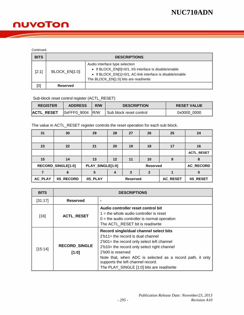
NUC710ADN
Publication Release Date: November23, 2013 - 295 - Revision A10
Continued.
BITS DESCRIPTIONS
[2:1] BLOCK_EN[1:0]
Audio interface type selection • If BLOCK_EN[0]=0/1, IIS interface is disable/enable • If BLOCK_EN[1]=0/1, AC-link interface is disable/enable
The BLOCK_EN[1:0] bits are read/write
[0] Reserved
Sub-block reset control register (ACTL_RESET)
REGISTER ADDRESS R/W DESCRIPTION RESET VALUE
ACTL_RESET 0xFFF0_9004 R/W Sub block reset control 0x0000_0000
The value in ACTL_RESET register controls the reset operation for each sub block.
BITS DESCRIPTIONS
[31:17] Reserved -
[16] ACTL_RESET
Audio controller reset control bit 1 = the whole audio controller is reset 0 = the audio controller is normal operation The ACTL_RESET bit is read/write
[15:14] RECORD_SINGLE
[1:0]
Record single/dual channel select bits 2’b11= the record is dual channel 2’b01= the record only select left channel 2’b10= the record only select right channel 2’b00 is reserved Note that, when ADC is selected as a record path, it only supports the left channel record. The PLAY_SINGLE [1:0] bits are read/write
31 30 29 28 27 26 25 24
23 22 21 20 19 18 17 16
ACTL_RESET
15 14 13 12 11 10 9 8
RECORD_SINGLE[1:0] PLAY_SINGLE[1:0] Reserved AC_RECORD
7 6 5 4 3 2 1 0
AC_PLAY IIS_RECORD IIS_PLAY Reserved AC_RESET IIS_RESET

NUC710ADN
Publication Release Date: November235, 2013 - 296 - Revision A10
Continued.
BITS DESCRIPTIONS
[13:12] PLAY_SINGLE
[1:0]
Playback single/dual channel select bits PLAY_SINGLE [1:0]=11, the playback is in stereo mode PLAY_SINGLE [1:0]=10, the playback is in mono mode PLAY_SINGLE [1:0]= 00 & 01 is reserved The PLAY_SINGLE [1:0] bits are read/write
[8] AC_RECORD
AC link record control bit AC_RECORD=0, the record path of AC link is disable AC_RECORD=1, the record path of AC link is enable The AC_RECORD bit is read/write
[7] AC_PLAY
AC link playback control bit AC_PLAY=0, the playback path of AC link is disable AC_PLAY=1, the playback path of AC link is enable The AC_PLAY bit is read/write
[6] IIS_RECORD
IIS record control bit IIS_RECORD=0, the record path of IIS is disable IIS_RECORD=1, the record path of IIS is enable The IIS_RECORD bit is read/write
[5] IIS_PLAY
IIS playback control bit IIS_PLAY=0, the playback path of IIS is disable IIS_PLAY=1, the playback path of IIS is enable The IIS_PLAY bit is read/write
[1] AC_RESET
AC link sub block RESET control bit AC_RESET=0, release the AC link function block from reset mode AC_RESET=1, force the AC link function block to reset mode The AC_RESET bit is read/write
[0] IIS_RESET
IIS sub block RESET control bit IIS_RESET=0, release the IIS function block from reset mode IIS_RESET=1, force the IIS function block to reset mode The IIS_RESET bit is read/write
DMA record destination base address (ACTL_RDSTB)
REGISTER ADDRESS R/W DESCRIPTION RESET VALUE
ACTL_RDSTB 0xFFF0_9008 R/W DMA record destination base address 0x0000_0000
The value in the ACTL_RDSTB register is the DMA record destination base address and can only be changed by the CPU.

NUC710ADN
Publication Release Date: November23, 2013 - 297 - Revision A10
BITS DESCRIPTIONS
[31:0] AUDIO_RDSTB[31:0] 32-bit record destination base address The AUDIO_RDSTB[31:0] bits is read/write.
DMA destination end address (ACTL_RDST_LENGTH)
REGISTER ADDRESS R/W DESCRIPTION RESET VALUE
ACTL_RDST_LENGTH 0xFFF0_900C R/W DMA record destination address length 0x0000_0000
The value in ACTL_RDST_LENGTH register is the record destination address length of DMA, and only the CPU can change the register.
BITS DESCRIPTIONS
[31:0] AUDIO_RDST_L[31:0] 32-bit record destination address length
The AUDIO_RDST_L[31:0] bits is read/write.
31 30 29 28 27 26 25 24 AUDIO_RDSTB[31:24]
23 22 21 20 19 18 17 16 AUDIO_RDSTB[23:16]
15 14 13 12 11 10 9 8 AUDIO_RDSTB[15:8]
7 6 5 4 3 2 1 0 AUDIO_RDSTB[7:0]
31 30 29 28 27 26 25 24 AUDIO_RDST_L[31:24]
23 22 21 20 19 18 17 16 AUDIO_RDST_L[23:16]
15 14 13 12 11 10 9 8 AUDIO_RDST_L[15:8]
7 6 5 4 3 2 1 0 AUDIO_RDST_L[7:0]

NUC710ADN
Publication Release Date: November235, 2013 - 298 - Revision A10
DMA destination current address (ACTL_RDSTC)
REGISTER ADDRESS R/W DESCRIPTION RESET VALUE
ACTL_RDSTC 0xFFF0_9010 RO DMA record destination current address 0x0000_0000
The value in ACTL_RDSTC is the DMA record destination current address. Only the CPU can read this register.
BITS DESCRIPTIONS
[31:0] AUDIO_RDSTC[31:0] 32-bit record destination current address The AUDIO_RDSTC[31:0] bits is read only.
Audio controller record status register (ACTL_RSR)
REGISTER ADDRESS R/W DESCRIPTION RESET VALUE
ACTL_RSR 0xFFF0_9014 R/W Audio controller FIFO and DMA status register for record 0x0000_0000
31 30 29 28 27 26 25 24 AUDIO_RDSTC[31:24]
23 22 21 20 19 18 17 16 AUDIO_RDSTC[23:16]
15 14 13 12 11 10 9 8 AUDIO_RDSTC[15:8]
7 6 5 4 3 2 1 0 AUDIO_RDSTC[7:0]
31 30 29 28 27 26 25 24
Reserved
23 22 21 20 19 18 17 16
Reserved
15 14 13 12 11 10 9 8
Reserved
7 6 5 4 3 2 1 0
Reserved R_FIFO_
FULL R_DMA_END_
IRQ R_DMA_MIDDLE_
IRQ
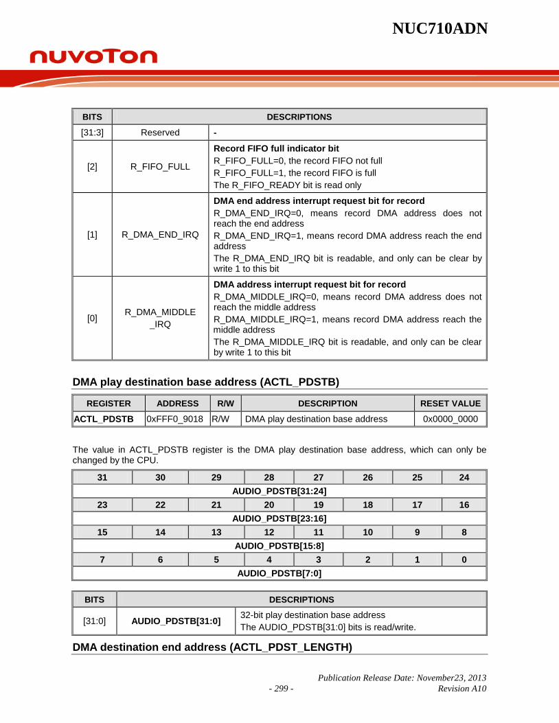
NUC710ADN
Publication Release Date: November23, 2013 - 299 - Revision A10
BITS DESCRIPTIONS
[31:3] Reserved -
[2] R_FIFO_FULL
Record FIFO full indicator bit R_FIFO_FULL=0, the record FIFO not full R_FIFO_FULL=1, the record FIFO is full The R_FIFO_READY bit is read only
[1] R_DMA_END_IRQ
DMA end address interrupt request bit for record R_DMA_END_IRQ=0, means record DMA address does not reach the end address R_DMA_END_IRQ=1, means record DMA address reach the end address The R_DMA_END_IRQ bit is readable, and only can be clear by write 1 to this bit
[0] R_DMA_MIDDLE
_IRQ
DMA address interrupt request bit for record R_DMA_MIDDLE_IRQ=0, means record DMA address does not reach the middle address R_DMA_MIDDLE_IRQ=1, means record DMA address reach the middle address The R_DMA_MIDDLE_IRQ bit is readable, and only can be clear by write 1 to this bit
DMA play destination base address (ACTL_PDSTB)
REGISTER ADDRESS R/W DESCRIPTION RESET VALUE
ACTL_PDSTB 0xFFF0_9018 R/W DMA play destination base address 0x0000_0000
The value in ACTL_PDSTB register is the DMA play destination base address, which can only be changed by the CPU.
BITS DESCRIPTIONS
[31:0] AUDIO_PDSTB[31:0] 32-bit play destination base address The AUDIO_PDSTB[31:0] bits is read/write.
DMA destination end address (ACTL_PDST_LENGTH)
31 30 29 28 27 26 25 24 AUDIO_PDSTB[31:24]
23 22 21 20 19 18 17 16 AUDIO_PDSTB[23:16]
15 14 13 12 11 10 9 8 AUDIO_PDSTB[15:8]
7 6 5 4 3 2 1 0 AUDIO_PDSTB[7:0]
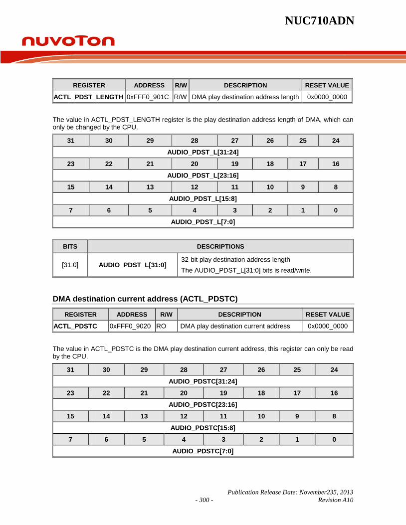
NUC710ADN
Publication Release Date: November235, 2013 - 300 - Revision A10
REGISTER ADDRESS R/W DESCRIPTION RESET VALUE
ACTL_PDST_LENGTH 0xFFF0_901C R/W DMA play destination address length 0x0000_0000
The value in ACTL_PDST_LENGTH register is the play destination address length of DMA, which can only be changed by the CPU.
BITS DESCRIPTIONS
[31:0] AUDIO_PDST_L[31:0] 32-bit play destination address length The AUDIO_PDST_L[31:0] bits is read/write.
DMA destination current address (ACTL_PDSTC)
REGISTER ADDRESS R/W DESCRIPTION RESET VALUE
ACTL_PDSTC 0xFFF0_9020 RO DMA play destination current address 0x0000_0000
The value in ACTL_PDSTC is the DMA play destination current address, this register can only be read by the CPU.
31 30 29 28 27 26 25 24
AUDIO_PDST_L[31:24]
23 22 21 20 19 18 17 16
AUDIO_PDST_L[23:16]
15 14 13 12 11 10 9 8
AUDIO_PDST_L[15:8]
7 6 5 4 3 2 1 0
AUDIO_PDST_L[7:0]
31 30 29 28 27 26 25 24
AUDIO_PDSTC[31:24]
23 22 21 20 19 18 17 16
AUDIO_PDSTC[23:16]
15 14 13 12 11 10 9 8
AUDIO_PDSTC[15:8]
7 6 5 4 3 2 1 0
AUDIO_PDSTC[7:0]
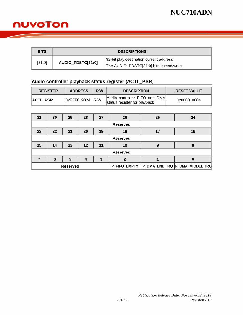
NUC710ADN
Publication Release Date: November23, 2013 - 301 - Revision A10
BITS DESCRIPTIONS
[31:0] AUDIO_PDSTC[31:0] 32-bit play destination current address The AUDIO_PDSTC[31:0] bits is read/write.
Audio controller playback status register (ACTL_PSR)
REGISTER ADDRESS R/W DESCRIPTION RESET VALUE
ACTL_PSR 0xFFF0_9024 R/W Audio controller FIFO and DMA status register for playback 0x0000_0004
31 30 29 28 27 26 25 24
Reserved
23 22 21 20 19 18 17 16
Reserved
15 14 13 12 11 10 9 8
Reserved
7 6 5 4 3 2 1 0
Reserved P_FIFO_EMPTY P_DMA_END_IRQ P_DMA_MIDDLE_IRQ
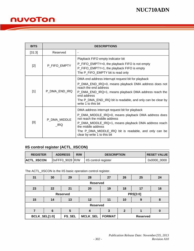
NUC710ADN
Publication Release Date: November235, 2013 - 302 - Revision A10
BITS DESCRIPTIONS
[31:3] Reserved -
[2] P_FIFO_EMPTY
Playback FIFO empty indicator bit P_FIFO_EMPTY=0, the playback FIFO is not empty P_FIFO_EMPTY=1, the playback FIFO is empty The P_FIFO_EMPTY bit is read only
[1] P_DMA_END_IRQ
DMA end address interrupt request bit for playback P_DMA_END_IRQ=0, means playback DMA address does not reach the end address P_DMA_END_IRQ=1, means playback DMA address reach the end address The P_DMA_END_IRQ bit is readable, and only can be clear by write 1 to this bit
[0] P_DMA_MIDDLE
_IRQ
DMA address interrupt request bit for playback P_DMA_MIDDLE_IRQ=0, means playback DMA address does not reach the middle address P_DMA_MIDDLE_IRQ=1, means playback DMA address reach the middle address The P_DMA_MIDDLE_IRQ bit is readable, and only can be clear by write 1 to this bit
IIS control register (ACTL_IISCON)
REGISTER ADDRESS R/W DESCRIPTION RESET VALUE
ACTL_IISCON 0xFFF0_9028 R/W IIS control register 0x0000_0000
The ACTL_IISCON is the IIS basic operation control register.
31 30 29 28 27 26 25 24
Reserved
23 22 21 20 19 18 17 16
Reserved PRS[3:0]
15 14 13 12 11 10 9 8
Reserved
7 6 5 4 3 2 1 0
BCLK_SEL[1:0] FS_SEL MCLK_SEL FORMAT Reserved
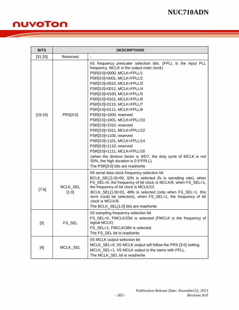
NUC710ADN
Publication Release Date: November23, 2013 - 303 - Revision A10
BITS DESCRIPTIONS
[31:20] Reserved -
[19:16] PRS[3:0]
IIS frequency prescaler selection bits. (FPLL is the input PLL frequency, MCLK is the output main clock) PSR[3:0]=0000, MCLK=FPLL/1 PSR[3:0]=0001, MCLK=FPLL/2 PSR[3:0]=0010, MCLK=FPLL/3 PSR[3:0]=0011, MCLK=FPLL/4 PSR[3:0]=0100, MCLK=FPLL/5 PSR[3:0]=0101, MCLK=FPLL/6 PSR[3:0]=0110, MCLK=FPLL/7 PSR[3:0]=0111, MCLK=FPLL/8 PSR[3:0]=1000, reserved PSR[3:0]=1001, MCLK=FPLL/10 PSR[3:0]=1010, reserved PSR[3:0]=1011, MCLK=FPLL/12 PSR[3:0]=1100, reserved PSR[3:0]=1101, MCLK=FPLL/14 PSR[3:0]=1110, reserved PSR[3:0]=1111, MCLK=FPLL/16 (when the division factor is 3/5/7, the duty cycle of MCLK is not 50%, the high duration is 0.5*FPLL) The PSR[3:0] bits are read/write
[7:6] BCLK_SEL [1:0]
IIS serial data clock frequency selection bit BCLK_SEL[1:0]=00, 32fs is selected (fs is sampling rate), when FS_SEL=0, the frequency of bit clock is MCLK/8, when FS_SEL=1, the frequency of bit clock is MCLK/12. BCLK_SEL[1:0]=01, 48fs is selected (only when FS_SEL=1, this term could be selection), when FS_SEL=1, the frequency of bit clock is MCLK/8. The BCLK_SEL[1:0] bits are read/write
[5] FS_SEL
IIS sampling frequency selection bit FS_SEL=0, FMCLK/256 is selected (FMCLK is the frequency of signal MCLK) FS_SEL=1, FMCLK/384 is selected The FS_SEL bit is read/write
[4] MCLK_SEL
IIS MCLK output selection bit MCLK_SEL=0, IIS MCLK output will follow the PRS [3:0] setting. MCLK_SEL=1, IIS MCLK output is the same with FPLL. The MCLK_SEL bit is read/write

NUC710ADN
Publication Release Date: November235, 2013 - 304 - Revision A10
Continued
BITS DESCRIPTIONS
[3] FORMAT
IIS format selection bits FORMAT=0, IIS compatible format is selected FORMAT=1, MSB-justified format is selected The FORMAT bit is read/write
[2:0] Reserved -
AC-link Control Register (ACTL_ACCON)
REGISTER ADDRESS R/W DESCRIPTION RESET VALUE
ACTL_ACCON 0xFFF0_902C R/W AC-link control register 0x0000_0000
The ACTL_ACCON register is the AC-link basic operation control register.
BITS DESCRIPTIONS
[6] Reserved -
[5] AC_BCLK_PU_EN
This bit controls the AC_BCLK pin pull-high resister. AC_BCLK_PU_EN=0, the AC_BCLK pin pull-high resister is disabled AC_BCLK_PU_EN=1, the AC_BCLK pin pull-high resister is enabled The AC_BCLK_PU_EN bit is read/write.
[4] AC_R_FINISH
AC-link read data ready bit. When read data indexed by previous frame is shifted into ACTL_ACIS2, the AC_R_FINISH bit is automatically set to 1. After the CPU reads the data, AC_R_FINISH bit is cleared to 0. AC_R_FINISH=0, read data buffer has been read by CPU AC_R_FINISH=1, read data buffer is ready for CPU read The AC_R_FINISH bit is read only
31 30 29 28 27 26 25 24 Reserved
23 22 21 20 19 18 17 16 Reserved
15 14 13 12 11 10 9 8 Reserved
7 6 5 4 3 2 1 0
Reserved AC_BCLK_PU_EN AC_R_FINISH AC_W_FINISH AC_W_RES AC_C_RES Reserved

NUC710ADN
Publication Release Date: November23, 2013 - 305 - Revision A10
Continued.
BITS DESCRIPTIONS
[3] AC_W_FINISH
AC-link write frame finish bit. When writing data to register ACTL_ACOS0, the AC_W_FINISH bit is set to 1 automatically. After AC-link interface shift out the register ACTL_ACOS0, the AC_W_FINISH bit is cleared to 0. AC_W_FINISH=0, AC-link control data out buffer has been shifted to the codec by the CPU and data buffer is empty. AC_W_FINISH=1, AC-link control data out buffer is ready to be shifted (after the programmer has written the data into register ACTL_ACOS0) The AC_W_FINISH bit is read only
[2] AC_W_RES
AC-link warm reset control bit. When this bit is set to 1, (AC-link begins the ‘warm reset procedure’, and then automatically clears this bit) the interface signal AC_SYNC is high, when this bit is set to 0, the interface signal AC_SYNC is controlled by AC_BCLK input when this bit is set to 1. Note the AC-link spec. shows it needs at least 10 us high duration of AC_SYNC to warm reset AC97. AC_W_RES=0, AC_SYNC pin is controlled by AC_BCLK input pin AC_W_RES=1, AC_SYNC pin is forced to high The AC_W_RES bit is read/write
[1] AC_C_RES
AC-link cold reset control bit, when this bit is set to 1, the interface signal AC_RESETB is low, when this bit is set to 0, the signal AC_RESETB is high. Note the AC-link spec. shows it needs at least 10 us low duration of AC_RESETB to cold reset AC97. AC_C_RES=0, AC_RESETB pin is set to 1 AC_C_RES=1, AC_RESETB pin is set to 0 The AC_C_RES bit is read/write
[0] Reserved -
AC-link output slot 0 (ACTL_ACOS0)
REGISTER ADDRESS R/W DESCRIPTION RESET VALUE
ACTL_ACOS0 0xFFF0_9030 R/W AC-link out slot 0 0x0000_0000
The ACTL_ACOS0 register stores slot 0 value to be shifted by AC-link. Note that writing data to ACTL_ACOS0 register when AC_W_FINISH bit (ACTL_ACCON[3]) is set is invalid. Therefore, check AC_W_FINISH bit status before write data into ACTL_ACOS0 register.

NUC710ADN
Publication Release Date: November235, 2013 - 306 - Revision A10
BITS DESCRIPTIONS
[31:5] Reserved -
[4] VALID_FRAME
Frame valid indicated bits VALID_FRAME=1, any one of slot is valid VALID_FRAME=0, no any slot is valid The VALID_FRAME bits are read/write
[3:0] SLOT_VALID
[3:0]
Slot valid indicated bits SLOT_VALID[0]= 1/0, indicate Slot 1 valid/invalid SLOT_VALID[1]= 1/0, indicate Slot 2 valid/invalid SLOT_VALID[2]= 1/0, indicate Slot 3 valid/invalid SLOT_VALID[3]= 1/0, indicate Slot 4 valid/invalid The SLOT_VALID[3:0] bits are read/write
The AC-link output slot 1 (ACTL_ACOS1)
REGISTER ADDRESS R/W DESCRIPTION RESET VALUE
ACTL_ACOS1 0xFFF0_9034 R/W AC-link out slot 1 0x0000_0080
The ACTL_ACOS1 register stores slot 1 value to be shifted by the AC-link.
31 30 29 28 27 26 25 24
Reserved
23 22 21 20 19 18 17 16
Reserved
15 14 13 12 11 10 9 8
Reserved
7 6 5 4 3 2 1 0
Reserved VALID_ FRAME SLOT_VALID[3:0]

NUC710ADN
Publication Release Date: November23, 2013 - 307 - Revision A10
BITS DESCRIPTIONS
[31:8] Reserved -
[7] R_WB
Read/Write select bit R_WB=1, a read specified by R_INDEX [6:0] will occur, and the data will appear in the next frame R_WB=0, a write specified by R_INDEX [6:0] will occur, and the write data is put at slot 2 The R_WB bit is read/write
[6:0] R_INDEX[6:0] External AC97 CODEC control register index (address) bits The R_INDEX [6:0] bits are read/write
AC-link output slot 2 (ACTL_ACOS2)
REGISTER ADDRESS R/W DESCRIPTION RESET VALUE
ACTL_ACOS2 0xFFF0_9038 R/W AC-link out slot 2 0x0000_0000
The ACTL_ACOS2 register store the slot 2 value to be shifted by the AC-link.
BITS DESCRIPTIONS
31 30 29 28 27 26 25 24
Reserved
23 22 21 20 19 18 17 16
Reserved
15 14 13 12 11 10 9 8
Reserved
7 6 5 4 3 2 1 0
R_WB R_INDEX [6:0]
31 30 29 28 27 26 25 24
Reserved
23 22 21 20 19 18 17 16
Reserved
15 14 13 12 11 10 9 8
WD [15:8]
7 6 5 4 3 2 1 0
WD [7:0]

NUC710ADN
Publication Release Date: November235, 2013 - 308 - Revision A10
[31:0] Reserved -
[15:0] WD [15:0] AC-link write data The WD [15:0] bits are read/write
AC-link input slot 0 (ACTL_ACIS0)
REGISTER ADDRESS R/W DESCRIPTION RESET VALUE
ACTL_ACIS0 0xFFF0_903C R AC-link in slot 0 0x0000_0000
The ACTL_ACIS0 store the shift in slot 0 data of AC-link.
BITS DESCRIPTIONS
[31:5] Reserved -
[4] CODEC_READY
External AC97 audio CODEC ready bit CODEC_READY=0, indicates external AC97 audio CODEC is not ready CODEC_READY=1, indicates external AC97 audio CODEC is ready The CODEC_READY bit is read only
[3:0] SLOT_VALID[3:0]
Slot valid indicated bits SLOT_VALID[0]= 1/0, indicate Slot 1 valid/invalid SLOT_VALID[1]= 1/0, indicate Slot 2 valid/invalid SLOT_VALID[2]= 1/0, indicate Slot 3 valid/invalid SLOT_VALID[3]= 1/0, indicate Slot 4 valid/invalid The SLOT_VALID[3:0] bits are read
31 30 29 28 27 26 25 24
Reserved
23 22 21 20 19 18 17 16
Reserved
15 14 13 12 11 10 9 8
Reserved
7 6 5 4 3 2 1 0
Reserved CODEC_READY SLOT_VALID[3:0]

NUC710ADN
Publication Release Date: November23, 2013 - 309 - Revision A10
AC-link input slot 1 (ACTL_ACIS1)
REGISTER ADDRESS R/W DESCRIPTION RESET VALUE
ACTL_ACIS1 0xFFF0_9040 R AC-link in slot 1 0x0000_0000
The ACTL_ACIS1 stores the shift in slot 1 data of AC-link.
BITS DESCRIPTIONS
[31:9] Reserved -
[8:2] R_INDEX [6:0] Register index. The R_INDEX [6:0] echo the register index (address) when a register read has been requested in the previous frame. The R_INDEX [6:0] bits are read only
[1:0] SLOT_REQ [1:0]
Slot request. Indicates if the external codec need new PCM data that will transfer to the next frame. Any bit in SLOT_REQ [1:0] is set to 1, and indicates the external codec does not need a new sample in the corresponding slot[3:4] of the next frame Any SLOT_REQ [1:0] is clear to 0, indicate external codec need a new sample in the corresponding slot [3:4] of the next frame The SLOT_REQ [1:0] bits are read only
31 30 29 28 27 26 25 24
Reserved
23 22 21 20 19 18 17 16
Reserved
15 14 13 12 11 10 9 8
Reserved R_INDEX[6]
7 6 5 4 3 2 1 0
R_INDEX[5:0] SLOT_REQ[1:0]

NUC710ADN
Publication Release Date: November235, 2013 - 310 - Revision A10
AC-link input slot 2 (ACTL_ACIS2)
REGISTER ADDRESS R/W DESCRIPTION RESET VALUE
ACTL_ACIS2 0xFFF0_9044 R AC-link in slot 2 0x0000_0000
The ACTL_ACIS2 stores the shift in slot 2 data of AC-link.
BITS DESCRIPTIONS
[31:16] Reserved -
[15:0] RD[15:0] AC-link read data. The RD[15:0] bits are read only
31 30 29 28 27 26 25 24
Reserved
23 22 21 20 19 18 17 16
Reserved
15 14 13 12 11 10 9 8
RD[15:8]
7 6 5 4 3 2 1 0
RD[7:0]

NUC710ADN
Publication Release Date: November23, 2013 - 311 - Revision A10
6.12 Universal Asynchronous Receiver/Transmitter Controller Asynchronous serial communication block includes 4 UART blocks and accessory logic. They can be described as follows:
• UART0
A general purpose UART that does not include any accessory function. Clock Source : 15MHz UART Type : general UART, FIFO Number : 16-byte receiving FIFO and 16 byte transmitting FIFO Modem Function : N/A Accessory Function : N/A
• UART1
Designed for general-purpose UART or Bluetooth transceiver. It includes a high speed UART block with 64-byte receiving FIFO and 64-byte transmitting FIFO. It includes 3 clock sources: 15M, 30M, and 43.6M. The programmer is free to choose the clock source and divisor number for suitable baud rate.
Clock Source : 15MHz from external crystal 30MHz, 43.6MHz, 48MHz, 60MHz (optional function for Bluetooth HCI transport layer)
UART Type : high speed UART, FIFO Number : 64-byte receiving FIFO and 64 byte transmitting FIFO Modem Function : CTS and RTS (optional for Bluetooth. If they were enabled, TX & RX
in UART2 is cut off) Accessory Function : Bluetooth (optional) Baud Rate (max) : 1.875MHz I/O pin : TXD1, RXD1, RTS, CTS (optional)
• UART2
Designed for general purpose UART or IrDA SIR. The part of UART includes 16-byte receiving FIFO and 16-byte transmitting FIFO. The UART2 has no modem function. The UART2 block has merely 2 I/O. TXD2/RXD2 of UART2 occupies the same pins with RTS and CTS of UART1. Once the Bluetooth function has been enabled, UART2 should be disabled.
Clock Source : 15MHz UART Type : general UART, FIFO Number : 16-byte receiving FIFO and 16 byte transmitting FIFO Modem Function : N/A
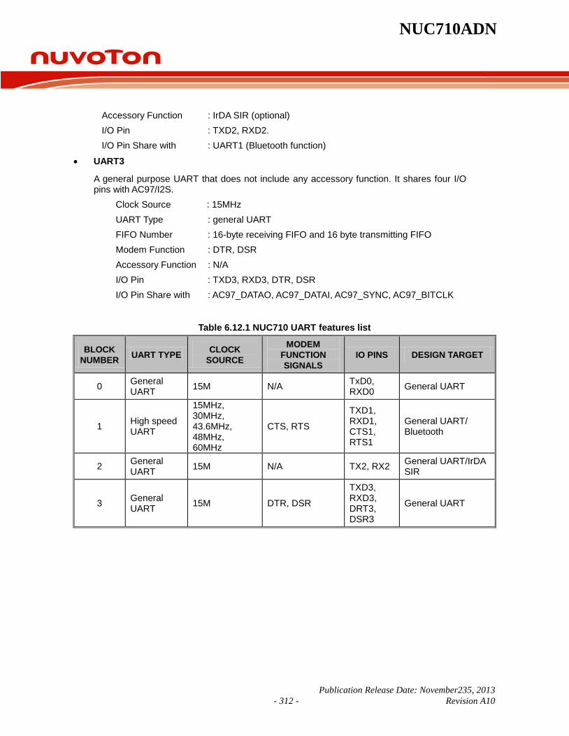
NUC710ADN
Publication Release Date: November235, 2013 - 312 - Revision A10
Accessory Function : IrDA SIR (optional) I/O Pin : TXD2, RXD2. I/O Pin Share with : UART1 (Bluetooth function)
• UART3
A general purpose UART that does not include any accessory function. It shares four I/O pins with AC97/I2S.
Clock Source : 15MHz UART Type : general UART FIFO Number : 16-byte receiving FIFO and 16 byte transmitting FIFO Modem Function : DTR, DSR Accessory Function : N/A I/O Pin : TXD3, RXD3, DTR, DSR I/O Pin Share with : AC97_DATAO, AC97_DATAI, AC97_SYNC, AC97_BITCLK
Table 6.12.1 NUC710 UART features list
BLOCK NUMBER UART TYPE CLOCK
SOURCE
MODEM FUNCTION SIGNALS
IO PINS DESIGN TARGET
0 General UART 15M N/A TxD0,
RXD0 General UART
1 High speed UART
15MHz, 30MHz, 43.6MHz, 48MHz, 60MHz
CTS, RTS
TXD1, RXD1, CTS1, RTS1
General UART/ Bluetooth
2 General UART 15M N/A TX2, RX2 General UART/IrDA
SIR
3 General UART 15M DTR, DSR
TXD3, RXD3, DRT3, DSR3
General UART

NUC710ADN
Publication Release Date: November23, 2013 - 313 - Revision A10
6.12.1 UART0 UART0 is a general UART block. It has no modem I/O signals. For a more detailed function description, please refer to section 7.12.5 General UART controller description
Table 6.12.1.1 UART0 Register Map
REGISTER ADDRESS R/W OTHER CONDITION RESET VALUE
UART0_RBR 0xFFF8_0000 R DLAB=0 Undefined
UART0_THR 0xFFF8_0000 W DLAB=0 Undefined
UART0_IER 0xFFF8_0004 R/W DLAB=0 0x0000_0000
UART0_DLL 0xFFF8_0000 R/W DLAB=1 0x0000_0000
UART0_DLM 0xFFF8_0004 R/W DLAB=1 0x0000_0000
UART0_IIR 0xFFF8_0008 R 0x8181_8181
UART0_FCR 0xFFF8_0008 W Undefined
UART0_LCR 0xFFF8_000c R/W 0x0000_0000
Reserved 0xFFF8_0010
UART0_LSR 0xFFF8_0014 R 0x6060_6060
Reserved 0xFFF8_0018
UART0_TOR 0xFFF8_001c R/W 0x0000_0000
6.12.2 UART1 UART1 is designed for general purpose UART or Bluetooth HCI transport layer. It is a high speed UART with 64-byte receive FIFO and 64-byte transmit FIFO. To perform 1.875MHz maximum baud rate, UART1 has 5 clock sources, 15MHz, 30MHz, 43.6MHz, 48MHz, and 60MHz. The first one is from an external 15M-crystal clock and the others are divided from system PLL 480MHz output. For more details about high speed UART, please refer to next section 7.12.6 High Speed UART controller function description. The block UART1 offer 4 I/O signals, TX, RX, CTS, and RTS. CTS and RTS are used as flow control for Bluetooth. CTS and RTS share the same I/O pins with TX and RX in block UART2.

NUC710ADN
Publication Release Date: November235, 2013 - 314 - Revision A10
Table 6.12.2.1 UART1 Register Map
REGISTER ADDRESS R/W OTHER CONDITION RESET VALUE
UART1_RBR 0xFFF8_0100 R DLAB=0 Undefined
UART1_THR 0xFFF8_0100 W DLAB=0 Undefined
UART1_IER 0xFFF8_0104 R/W DLAB=0 0x0000_0000
UART1_DLL 0xFFF8_0100 R/W DLAB=1 0x0000_0000
UART1_DLM 0xFFF8_0104 R/W DLAB=1 0x0000_0000
UART1_IIR 0xFFF8_0108 R 0x8181_8181
UART1_FCR 0xFFF8_0108 W Undefined
UART1_LCR 0xFFF8_010c R/W 0x0000_0000
UART1_MCR 0xFFF8_0110 R/W 0x0000_0000
UART1_LSR 0xFFF8_0114 R 0x6060_6060
UART1_MSR 0xFFF8_0118 R 0x0000_0000
UART1_TOR 0xFFF8_011c R/W 0x0000_0000
UART1_UBCR 0xFFF8_0120 R/W 0x0000_0000
UART1 Bluetooth Control Register (UART1_UBCR)
REGISTER ADDRESS R/W DESCRIPTION RESET VALUE
UART1_UBCR 0xFFF8_0120 R/W UART 1 Bluetooth Control Register 0x0000_0000
31 30 29 28 27 26 25 24
Reserved
23 22 21 20 19 18 17 16
Reserved 15 14 13 12 11 10 9 8
Reserved 7 6 5 4 3 2 1 0
Reserved UBCR[2:0]

NUC710ADN
Publication Release Date: November23, 2013 - 315 - Revision A10
BITS DESCRIPTIONS
[31:3] Reserved -
[2:0] UBCR
UBCR is a 3 bits register which is used to select a clock source to generate suitable baud rate: 000: 15Mhz from external crystal 100: 30Mhz divided from PLL 480Mhz 101: 43.6Mhz divided from PLL 480Mhz 110: 48Mhz divided from PLL 480Mhz 111: 60Mhz divided from PLL 480Mhz
6.12.3 UART2 UART2 contains 2 features: general UART and IrDA SIR decoder/encoder. UART has no modem function. Please read the spec of section 6.12.5 General UART controller function description. The IrDA SIR is described as follows:
Table 6.12.3.1 UART2 Register Map
REGISTER ADDRESS R/W OTHER CONDITION RESET VALUE
UART2_RBR 0xFFF8_0200 R DLAB=0 Undefined
UART2_THR 0xFFF8_0200 W DLAB=0 Undefined
UART2_IER 0xFFF8_0204 R/W DLAB=0 0x0000_0000
UART2_DLL 0xFFF8_0200 R/W DLAB=1 0x0000_0000
UART2_DLM 0xFFF8_0204 R/W DLAB=1 0x0000_0000
UART2_IIR 0xFFF8_0208 R 0x8181_8181
UART2_FCR 0xFFF8_0208 W Undefined
UART2_LCR 0xFFF8_020C R/W 0x0000_0000
Reserved 0xFFF8_0210 Undefined
UART2_LSR 0xFFF8_0214 R 0x6060_6060
Reserved 0xFFF8_0218 Undefined
UART2_TOR 0xFFF8_021C R/W 0x0000_0000
UART2_IRCR 0xFFF8_0220 R/W 0x0000_0040
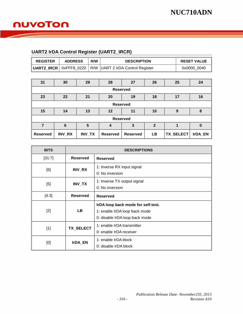
NUC710ADN
Publication Release Date: November235, 2013 - 316 - Revision A10
UART2 IrDA Control Register (UART2_IRCR)
REGISTER ADDRESS R/W DESCRIPTION RESET VALUE
UART2_IRCR 0xFFF8_0220 R/W UART 2 IrDA Control Register 0x0000_0040
31 30 29 28 27 26 25 24
Reserved
23 22 21 20 19 18 17 16
Reserved 15 14 13 12 11 10 9 8
Reserved 7 6 5 4 3 2 1 0
Reserved INV_RX INV_TX Reserved Reserved LB TX_SELECT IrDA_EN
BITS DESCRIPTIONS
[31:7] Reserved Reserved
[6] INV_RX 1: Inverse RX input signal 0: No inversion
[5] INV_TX 1: Inverse TX output signal 0: No inversion
[4:3] Reserved Reserved
[2] LB IrDA loop back mode for self-test. 1: enable IrDA loop back mode 0: disable IrDA loop back mode
[1] TX_SELECT 1: enable IrDA transmitter 0: enable IrDA receiver
[0] IrDA_EN 1: enable IrDA block 0: disable IrDA block
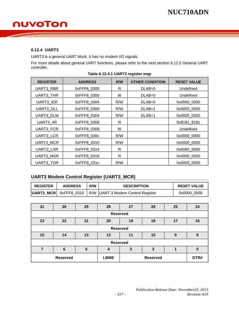
NUC710ADN
Publication Release Date: November23, 2013 - 317 - Revision A10
6.12.4 UART3 UART3 is a general UART block. It has no modem I/O signals. For more details about general UART functions, please refer to the next section 6.12.5 General UART controller.
Table 6.12.4.1 UART3 register map
REGISTER ADDRESS R/W OTHER CONDITION RESET VALUE
UART3_RBR 0xFFF8_0300 R DLAB=0 Undefined
UART3_THR 0xFFF8_0300 W DLAB=0 Undefined
UART3_IER 0xFFF8_0304 R/W DLAB=0 0x0000_0000
UART3_DLL 0xFFF8_0300 R/W DLAB=1 0x0000_0000
UART3_DLM 0xFFF8_0304 R/W DLAB=1 0x0000_0000
UART3_IIR 0xFFF8_0308 R 0x8181_8181
UART3_FCR 0xFFF8_0308 W Undefined
UART3_LCR 0xFFF8_030c R/W 0x0000_0000
UART3_MCR 0xFFF8_0310 R/W 0x0000_0000
UART3_LSR 0xFFF8_0314 R 0x6060_6060
UART3_MSR 0xFFF8_0318 R 0x0000_0000
UART3_TOR 0xFFF8_031c R/W 0x0000_0000
UART3 Modem Control Register (UART3_MCR)
REGISTER ADDRESS R/W DESCRIPTION RESET VALUE
UART3_MCR 0xFFF8_0310 R/W UART 3 Modem Control Register 0x0000_0000
31 30 29 28 27 26 25 24
Reserved
23 22 21 20 19 18 17 16
Reserved 15 14 13 12 11 10 9 8
Reserved 7 6 5 4 3 2 1 0
Reserved LBME Reserved DTR#

NUC710ADN
Publication Release Date: November235, 2013 - 318 - Revision A10
UART3 Modem Status Register (UART3_MSR)
REGISTER ADDRESS R/W DESCRIPTION RESET VALUE
UART3_MSR 0xFFF8_0318 R UART 3 Modem Status Register 0x0000_0000
31 30 29 28 27 26 25 24
Reserved
23 22 21 20 19 18 17 16
Reserved 15 14 13 12 11 10 9 8
Reserved 7 6 5 4 3 2 1 0
Reserved Reserved DSR# Reserved Reserved Reserved DDSR Reserved
6.12.5 General UART Controller The Universal Asynchronous Receiver/Transmitter (UART) performs a serial-to-parallel conversion of data characters received from the peripheral such as MODEM, and a parallel-to-serial conversion of data characters received from the CPU. There are five types of interrupts, i.e., line status interrupt, transmitter FIFO empty interrupt, receiver threshold level reaching interrupt, time out interrupt, and MODEM status interrupt. One 16-byte transmitter FIFO (TX_FIFO) and one 16-byte (plus 3-bit of error data per byte) receiver FIFO (RX_FIFO) has been built in to reduce the number of interrupts presented to the CPU. The CPU can completely read the status of the UART at any time during the operation. The reported status information includes the type and condition of the transfer operations being performed by the UART, as well as any error conditions (parity, overrun, framing, or break interrupt) found. The UART includes a programmable baud rate generator that is capable of dividing crystal clock input by divisors to produce the clock the transmitter and receiver needs. The equation is
BaudOut = crystal clock / 16 * [Divisor + 2]. UART includes the following features: Transmitter and receiver are buffered with a 16-byte FIFO each to reduce the number of interrupts
presented to the CPU. Subset of MODEM control functions (DSR, DTR, by IP selection) Fully programmable serial-interface characteristics:
-- 5-, 6-, 7-, or 8-bit characters -- Even, odd, or no-parity bit generation and detection -- 1-, 1&1/2, or 2-stop bit generation -- Baud rate generation
Line break generation and detection False start bit detection
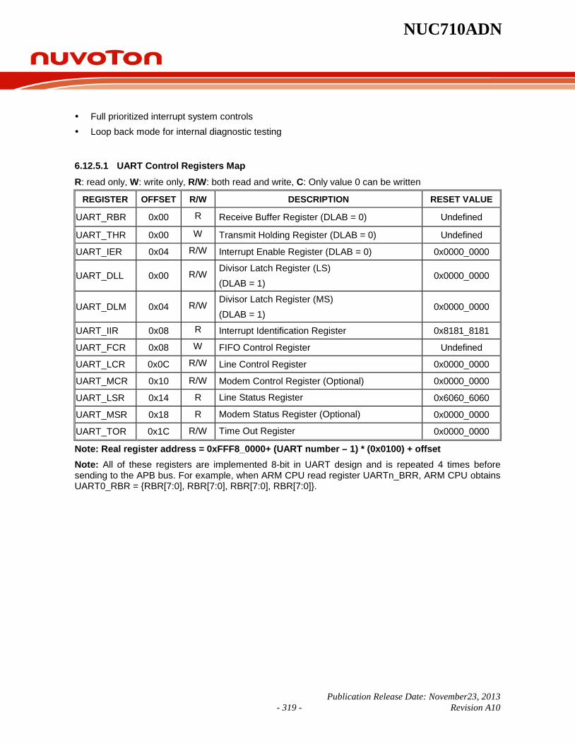
NUC710ADN
Publication Release Date: November23, 2013 - 319 - Revision A10
Full prioritized interrupt system controls Loop back mode for internal diagnostic testing
6.12.5.1 UART Control Registers Map R: read only, W: write only, R/W: both read and write, C: Only value 0 can be written
REGISTER OFFSET R/W DESCRIPTION RESET VALUE
UART_RBR 0x00 R Receive Buffer Register (DLAB = 0) Undefined
UART_THR 0x00 W Transmit Holding Register (DLAB = 0) Undefined
UART_IER 0x04 R/W Interrupt Enable Register (DLAB = 0) 0x0000_0000
UART_DLL 0x00 R/W Divisor Latch Register (LS) (DLAB = 1)
0x0000_0000
UART_DLM 0x04 R/W Divisor Latch Register (MS) (DLAB = 1)
0x0000_0000
UART_IIR 0x08 R Interrupt Identification Register 0x8181_8181
UART_FCR 0x08 W FIFO Control Register Undefined
UART_LCR 0x0C R/W Line Control Register 0x0000_0000
UART_MCR 0x10 R/W Modem Control Register (Optional) 0x0000_0000
UART_LSR 0x14 R Line Status Register 0x6060_6060
UART_MSR 0x18 R Modem Status Register (Optional) 0x0000_0000
UART_TOR 0x1C R/W Time Out Register 0x0000_0000
Note: Real register address = 0xFFF8_0000+ (UART number – 1) * (0x0100) + offset Note: All of these registers are implemented 8-bit in UART design and is repeated 4 times before sending to the APB bus. For example, when ARM CPU read register UARTn_BRR, ARM CPU obtains UART0_RBR = RBR[7:0], RBR[7:0], RBR[7:0], RBR[7:0].

NUC710ADN
Publication Release Date: November235, 2013 - 320 - Revision A10
UART Receive Buffer Register (UART_RBR)
REGISTER OFFSET R/W DESCRIPTION RESET VALUE
UART_RBR 0x00 R Receive Buffer Register (DLAB = 0) Undefined
31 30 29 28 27 26 25 24 Reserved
23 22 21 20 19 18 17 16 Reserved
15 14 13 12 11 10 9 8 Reserved
7 6 5 4 3 2 1 0 8-bit Received Data
BITS DESCRIPTIONS
[7:0] 8-bit Received Data By reading this register, the UART will return an 8-bit data received from SIN pin (LSB first).
UART Transmit Holding Register (UART_THR)
REGISTER OFFSET R/W DESCRIPTION RESET VALUE
UART_THR 0x00 W Transmit Holding Register (DLAB = 0) Undefined
31 30 29 28 27 26 25 24
Reserved 23 22 21 20 19 18 17 16
Reserved 15 14 13 12 11 10 9 8
Reserved 7 6 5 4 3 2 1 0
8-bit Transmitted Data
BITS DESCRIPTIONS
[7:0] 8-bit Transmitted Data By writing to this register, the UART will send out 8-bit data through the SOUT pin (LSB first).

NUC710ADN
Publication Release Date: November23, 2013 - 321 - Revision A10
UART Interrupt Enable Register (UART_IER)
REGISTER OFFSET R/W DESCRIPTION RESET VALUE
UART_IER 0x04 R/W Interrupt Enable Register (DLAB = 0) 0x0000_0000
31 30 29 28 27 26 25 24
Reserved
23 22 21 20 19 18 17 16
Reserved 15 14 13 12 11 10 9 8
Reserved 7 6 5 4 3 2 1 0
RESERVED nDBGACK_EN MSIE RLSIE THREIE RDAIE
BITS DESCRIPTIONS
[31:5] Reserved -
[4] nDBGACK_EN
ICE debug mode acknowledge enable 0 = When DBGACK is high, the UART receiver time-out clock is held 1 = No matter whether DBGACK is high or not, the UART receiver timer-out clock will not be held
[3] MSIE Modem Status Interrupt (Irpt_MOS) Enable 0 = Mask off Irpt_MOS 1 = Enable Irpt_MOS
[2] RLSIE Receive Line Status Interrupt (Irpt_RLS) Enable 0 = Mask off Irpt_RLS 1 = Enable Irpt_RLS
[1] THREIE
Transmit Holding Register Empty Interrupt (Irpt_THRE) Enable 0 = Mask off Irpt_THRE 1 = Enable Irpt_THRE
[0] RDAIE
Receive Data Available Interrupt (Irpt_RDA) Enable and Time-out Interrupt (Irpt_TOUT) Enable 0 = Mask off Irpt_RDA and Irpt_TOUT 1 = Enable Irpt_RDA and Irpt_TOUT

NUC710ADN
Publication Release Date: November235, 2013 - 322 - Revision A10
UART Divider Latch (Low Byte) Register (UART_DLL)
REGISTER OFFSET R/W DESCRIPTION RESET VALUE
UART_DLL 0x00 R/W Divisor Latch Register (LS) (DLAB = 1) 0x0000_0000
31 30 29 28 27 26 25 24
Reserved 23 22 21 20 19 18 17 16
Reserved 15 14 13 12 11 10 9 8
Reserved 7 6 5 4 3 2 1 0
Baud Rate Divider (Low Byte)
BITS DESCRIPTIONS
[7:0] Baud Rate Divider (Low Byte) The low byte of the baud rate divider
UART Divisor Latch (High Byte) Register (UART_DLM)
REGISTER OFFSET R/W DESCRIPTION RESET VALUE
UART_DLM 0x04 R/W Divisor Latch Register (MS) (DLAB = 1) 0x0000_0000
31 30 29 28 27 26 25 24 Reserved
23 22 21 20 19 18 17 16 Reserved
15 14 13 12 11 10 9 8 Reserved
7 6 5 4 3 2 1 0 Baud Rate Divider (High Byte)
BITS DESCRIPTIONS
[7:0] Baud Rate Divider (High Byte) The high byte of the baud rate divider
This 16-bit divider DLM, DLL is used to determine the baud rate as follows Baud Rate = Crystal Clock / 16 * [Divisor + 2]
Note: This definition is different from 16550

NUC710ADN
Publication Release Date: November23, 2013 - 323 - Revision A10
UART Interrupt Identification Register (UART_IIR)
REGISTER OFFSET R/W DESCRIPTION RESET VALUE
UART_IIR 0x08 R Interrupt Identification Register 0x8181_8181
31 30 29 28 27 26 25 24
Reserved
23 22 21 20 19 18 17 16
Reserved 15 14 13 12 11 10 9 8
Reserved 7 6 5 4 3 2 1 0
FMES RFTLS DMS IID NIP
BITS DESCRIPTIONS
[7] FMES
FIFO Mode Enable Status This bit indicates whether FIFO mode is enabled or not. Since FIFO mode is always enabled, this bit always shows a logical 1 when the CPU reads this register.
[6:5] RFTLS RX FIFO Threshold Level Status These bits show the current setting of receiver FOFO threshold level (RTHO). The meaning of RTHO is defined in the following FCR description.
[4] DMS DMA Mode Select DMA function is not implemented in this version. When reading IIR, the DMS always returns 0.
[3:1] IID Interrupt Identification The IID together with NIP indicates the current interrupt request from UART
[0] NIP No Interrupt Pending There is no pending interrupt.

NUC710ADN
Publication Release Date: November235, 2013 - 324 - Revision A10
Table 6.12.5.1 Interrupt Control Functions
IIR [3:0] PRIORITY INTERRUPT TYPE INTERRUPT SOURCE INTERRUPT RESET
CONTROL
- - - 1 -- None None --
0110 Highest Receiver Line Status (Irpt_RLS)
Overrun error, parity error, framing error, or break interrupt
Reading the LSR
0100 Second Received Data
Available (Irpt_RDA)
Receiver FIFO threshold level is reached
Receiver FIFO drops below the threshold level
1100 Second Receiver FIFO
Time-out (Irpt_TOUT)
Receiver FIFO is non-empty and no activity occurred during the TOR defined time duration
Reading the RBR
0010 Third
Transmitter Holing Register
Empty (Irpt_THRE)
Transmitter holding register empty
Reading the IIR (if source of interrupt is Irpt_THRE) or writing into the THR
0000 Fourth MODEM Status (Irpt_MOS)
The CTS, DSR, or DCD bits are changing state or the RI bit is changing from high to low.
Reading the MSR (optional)
Note: These definitions of bit 7, bit 6, bit 5, and bit 4 are different from the 16550
UART FIFO Control Register (UART_FCR)
REGISTER OFFSET R/W DESCRIPTION RESET VALUE
UART_FCR 0x08 W FIFO Control Register Undefined
31 30 29 28 27 26 25 24
Reserved
23 22 21 20 19 18 17 16
Reserved 15 14 13 12 11 10 9 8
Reserved 7 6 5 4 3 2 1 0
RFITL RESERVED DMS TFR RFR FME

NUC710ADN
Publication Release Date: November23, 2013 - 325 - Revision A10
BITS DESCRIPTIONS
[7:6] RFITL
RX FIFO Interrupt (Irpt_RDA) Trigger Level RFITL [7:6] Irpt_RDA Trigger Level (Bytes)
00 01
01 04
10 08
11 14
[3] DMS DMA Mode Select The DMA function is not implemented in this version.
[2] TFR TX FIFO Reset Setting this bit generates an OSC cycle reset pulse to reset TX FIFO. The TX FIFO becomes empty (TX pointer is reset to 0) after such reset. This bit is returned to 0 automatically after the reset pulse is generated.
[1] RFR RX FIFO Reset Setting this bit will generate an OSC cycle reset pulse to reset RX FIFO. The RX FIFO becomes empty (RX pointer is reset to 0) after such reset. This bit is returned to 0 automatically after the reset pulse is generated.
[0] FME FIFO Mode Enable Because UART is always operating in the FIFO mode, writing this bit has no effect while reading always receives a logical 1. This bit must be 1 when other FCR bits are written to; otherwise, they will not be programmed.
UART Line Control Register (UART_LCR)
REGISTER OFFSET R/W DESCRIPTION RESET VALUE
UART_LCR 0x0C R/W Line Control Register 0x0000_0000
31 30 29 28 27 26 25 24 Reserved
23 22 21 20 19 18 17 16 Reserved
15 14 13 12 11 10 9 8 Reserved
7 6 5 4 3 2 1 0 DLAB BCB SPE EPE PBE NSB WLS
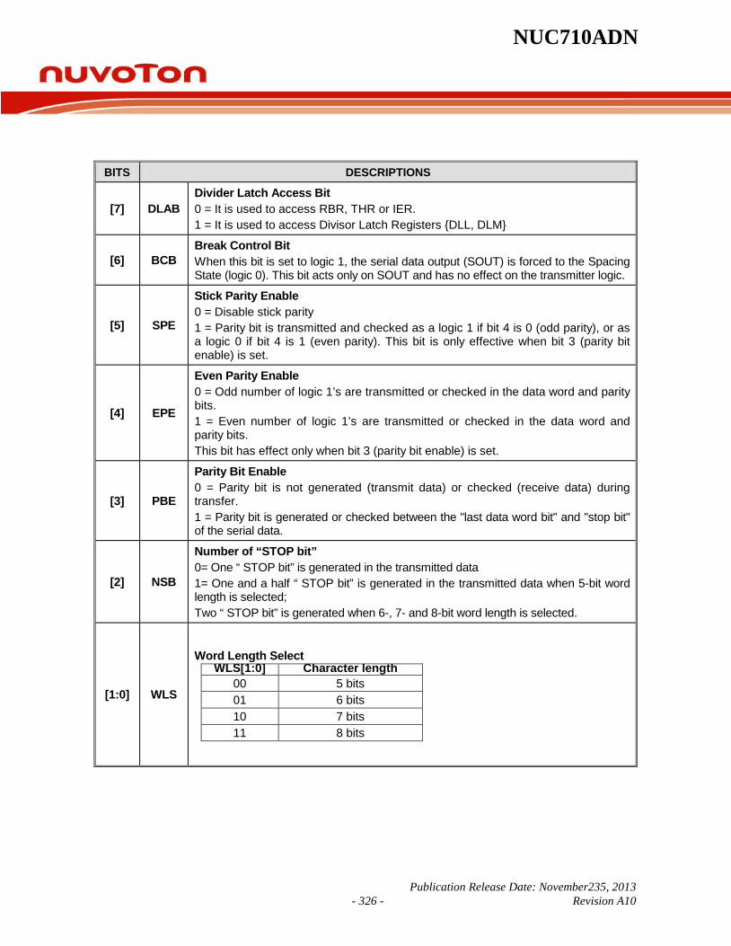
NUC710ADN
Publication Release Date: November235, 2013 - 326 - Revision A10
BITS DESCRIPTIONS
[7] DLAB Divider Latch Access Bit 0 = It is used to access RBR, THR or IER. 1 = It is used to access Divisor Latch Registers DLL, DLM
[6] BCB Break Control Bit When this bit is set to logic 1, the serial data output (SOUT) is forced to the Spacing State (logic 0). This bit acts only on SOUT and has no effect on the transmitter logic.
[5] SPE
Stick Parity Enable 0 = Disable stick parity 1 = Parity bit is transmitted and checked as a logic 1 if bit 4 is 0 (odd parity), or as a logic 0 if bit 4 is 1 (even parity). This bit is only effective when bit 3 (parity bit enable) is set.
[4] EPE
Even Parity Enable 0 = Odd number of logic 1’s are transmitted or checked in the data word and parity bits. 1 = Even number of logic 1’s are transmitted or checked in the data word and parity bits. This bit has effect only when bit 3 (parity bit enable) is set.
[3] PBE
Parity Bit Enable 0 = Parity bit is not generated (transmit data) or checked (receive data) during transfer. 1 = Parity bit is generated or checked between the "last data word bit" and "stop bit" of the serial data.
[2] NSB
Number of “STOP bit” 0= One “ STOP bit” is generated in the transmitted data 1= One and a half “ STOP bit” is generated in the transmitted data when 5-bit word length is selected; Two “ STOP bit” is generated when 6-, 7- and 8-bit word length is selected.
[1:0] WLS
Word Length Select WLS[1:0] Character length
00 5 bits 01 6 bits 10 7 bits 11 8 bits

NUC710ADN
Publication Release Date: November23, 2013 - 327 - Revision A10
UART Modem Control Register (UART_MCR)
REGISTER OFFSET R/W DESCRIPTION RESET VALUE
UART_MCR 0x10 R/W Modem Control Register (Optional) 0x0000_0000
31 30 29 28 27 26 25 24
Reserved
23 22 21 20 19 18 17 16
Reserved
15 14 13 12 11 10 9 8
Reserved
7 6 5 4 3 2 1 0
Reserved LBME Reserve Reserve Reserved DTR#
BITS DESCRIPTIONS
[31:5] Reserved -
[4] LBME
Loop-back Mode Enable 0 = Disable 1 = When the loop-back mode is enabled, the following signals are connected
internally SOUT connected to SIN and SOUT pin fixed at logic 1 DTR# connected to DSR# and DTR# pin fixed at logic 1
[3:1] Reserved -
[0] DTR Complement version of DTR# (Data-Terminal-Ready) signal Writing 0x00 to MCR, the DTR# bit are set to logic 1’s; Writing 0x0f to MCR, the DTR# bit are reset to logic 0’s.
UART Line Status Control Register (UART_LSR)
REGISTER OFFSET R/W DESCRIPTION RESET VALUE
UART_LSR 0x14 R Line Status Register 0x6060_6060
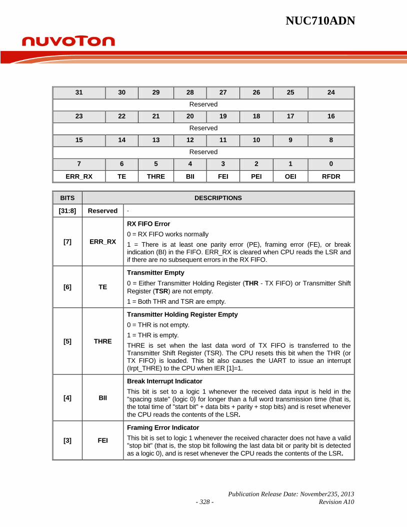
NUC710ADN
Publication Release Date: November235, 2013 - 328 - Revision A10
31 30 29 28 27 26 25 24
Reserved
23 22 21 20 19 18 17 16
Reserved
15 14 13 12 11 10 9 8
Reserved
7 6 5 4 3 2 1 0
ERR_RX TE THRE BII FEI PEI OEI RFDR
BITS DESCRIPTIONS
[31:8] Reserved -
[7] ERR_RX
RX FIFO Error 0 = RX FIFO works normally 1 = There is at least one parity error (PE), framing error (FE), or break indication (BI) in the FIFO. ERR_RX is cleared when CPU reads the LSR and if there are no subsequent errors in the RX FIFO.
[6] TE
Transmitter Empty 0 = Either Transmitter Holding Register (THR - TX FIFO) or Transmitter Shift Register (TSR) are not empty. 1 = Both THR and TSR are empty.
[5] THRE
Transmitter Holding Register Empty 0 = THR is not empty. 1 = THR is empty. THRE is set when the last data word of TX FIFO is transferred to the Transmitter Shift Register (TSR). The CPU resets this bit when the THR (or TX FIFO) is loaded. This bit also causes the UART to issue an interrupt (Irpt_THRE) to the CPU when IER [1]=1.
[4] BII
Break Interrupt Indicator This bit is set to a logic 1 whenever the received data input is held in the "spacing state" (logic 0) for longer than a full word transmission time (that is, the total time of "start bit" + data bits + parity + stop bits) and is reset whenever the CPU reads the contents of the LSR.
[3] FEI
Framing Error Indicator This bit is set to logic 1 whenever the received character does not have a valid "stop bit" (that is, the stop bit following the last data bit or parity bit is detected as a logic 0), and is reset whenever the CPU reads the contents of the LSR.

NUC710ADN
Publication Release Date: November23, 2013 - 329 - Revision A10
Continued.
BITS DESCRIPTIONS
[2] PEI Parity Error Indicator This bit is set to logic 1 whenever the received character does not have a valid "parity bit", and is reset whenever the CPU reads the contents of the LSR.
[1] OEI
Overrun Error Indicator An overrun error will occur only after the RX FIFO is full and the next character has been completely received in the shift register. The character in the shift register is overwritten, but it is not transferred to the RX FIFO. OE is indicated to the CPU as soon as it happens and is reset whenever the CPU reads the contents of the LSR.
[0] RFDR RX FIFO Data Ready 0 = RX FIFO is empty 1 = RX FIFO contains at least 1 received data word.
LSR [4:2] (BII, FEI, PEI) are revealed to the CPU when its associated character is at the top of the RX FIFO. These three error indicators are reset whenever the CPU reads the contents of the LSR. LSR [4:1] (BII, FEI, PEI, OEI) are the error conditions that produce a "receiver line status interrupt" (Irpt_RLS) when IER [2]=1. Reading LSR clears Irpt_RLS. Writing LSR is a null operation (not suggested)
UART Modem Status Register (UART_MSR)
REGISTER OFFSET R/W DESCRIPTION RESET VALUE
UART_MSR 0x18 R MODEM Status Register (Optional) 0x0000_0000
31 30 29 28 27 26 25 24
Reserved
23 22 21 20 19 18 17 16
Reserved
15 14 13 12 11 10 9 8
Reserved
7 6 5 4 3 2 1 0
Reserved Reserved DSR# Reserved Reserved Reserved DDSR Reserved

NUC710ADN
Publication Release Date: November235, 2013 - 330 - Revision A10
BITS DESCRIPTIONS [31:6] Reserved -
[5] DSR# Complement version of data set ready (DSR#) input (This bit is selected by IP)
[4:2] Reserved -
[1] DDSR DSR# State Change (This bit is selected by IP) This bit is set whenever DSR# input has changed state, and it is reset if the CPU reads the MSR.
[0] Reserved - Whenever any of MSR [3:0] is set to logic 1, a Modem Status Interrupt is generated if IER[3]=1. Writing MSR is a null operation (not suggested).
UART Time Out Register (UART_TOR)
REGISTER OFFSET R/W DESCRIPTION RESET VALUE
UART_TOR 0x1C R/W Time Out Register 0x0000_0000
31 30 29 28 27 26 25 24 Reserved
23 22 21 20 19 18 17 16 Reserved
15 14 13 12 11 10 9 8 Reserved
7 6 5 4 3 2 1 0
TOIE TOIC
BITS DESCRIPTIONS
[31:8] Reserved -
[7] TOIE Time Out Interrupt Enable The feature of receiver time out interrupt is enabled when TOR [7] = IER[0] = 1.
[6:0] TOIC
Time Out Interrupt Comparator The time out counter resets and starts counting (the counting clock = baud rate) whenever the RX FIFO receives a new data word. Once the content of time out counter (TOUT_CNT) is equal to that of time out interrupt comparator (TOIC), a receiver time out interrupt (Irpt_TOUT) is generated if TOR [7] = IER [0] = 1. A new incoming data word or RX FIFO empty clears Irpt_TOUT.

NUC710ADN
Publication Release Date: November23, 2013 - 331 - Revision A10
6.12.6 High speed UART Controller The High Speed Universal Asynchronous Receiver/Transmitter (HS_UART) performs a serial-to-parallel conversion on data characters received from the peripheral, and a parallel-to-serial conversion on data characters received from the CPU. There are five types of interrupt trigger, they are, transmitter FIFO empty, receiver threshold level reaching, line status (overrun error, parity error, framing error or break), timeout, and modem status. One 64-byte transmitter FIFO (TX_FIFO) and one 64-byte (plus 3-bit of error data per byte) receiver FIFO (RX_FIFO) is built-in to reduce the number of interrupts presented to the CPU. The CPU can completely read the UART status any time during operation. The reported status information includes the type and condition of transfer operations being performed by the UART, as well as any error conditions (parity, overrun, framing, or break) found. The UART includes a programmable baud rate generator capable of dividing crystal clock input to produce the needed clock for the transmitter and receiver. The equation is:
Baud Out = crystal clock / 16 * [Divisor + 2].
The UART includes the following features:
Transmitter and receiver are buffered with a 64-byte FIFO each to reduce the number of interrupts presented to the CPU.
Subset of MODEM control function (selected by IP) Fully programmable serial-interface characteristics:
5-, 6-, 7-, or 8-bit character
Even, odd, or no-parity bit generation and detection
1-, 1&1/2, or 2-stop bit generation
Baud rate generation
False start bit detection Full-prioritized interrupt system control Loop back mode not supported
6.12.6.1 High Speed UART Control Registers Map R: read only, W: write only, R/W: both read and write, C: Only value 0 can be written
REGISTER OFFSET R/W DESCRIPTION RESET VALUE
HSUART_RBR 0x00 R Receive Buffer Register (DLAB = 0) Undefined
HSUART_THR 0x00 W Transmit Holding Register (DLAB = 0) Undefined
HSUART_IER 0x04 R/W Interrupt Enable Register (DLAB = 0) 0x0000_0000
HSUART_DLL 0x00 R/W Divisor Latch Register (LS)(DLAB = 1) 0x0000_0000
HSUART_DLM 0x04 R/W Divisor Latch Register (MS)(DLAB = 1) 0x0000_0000
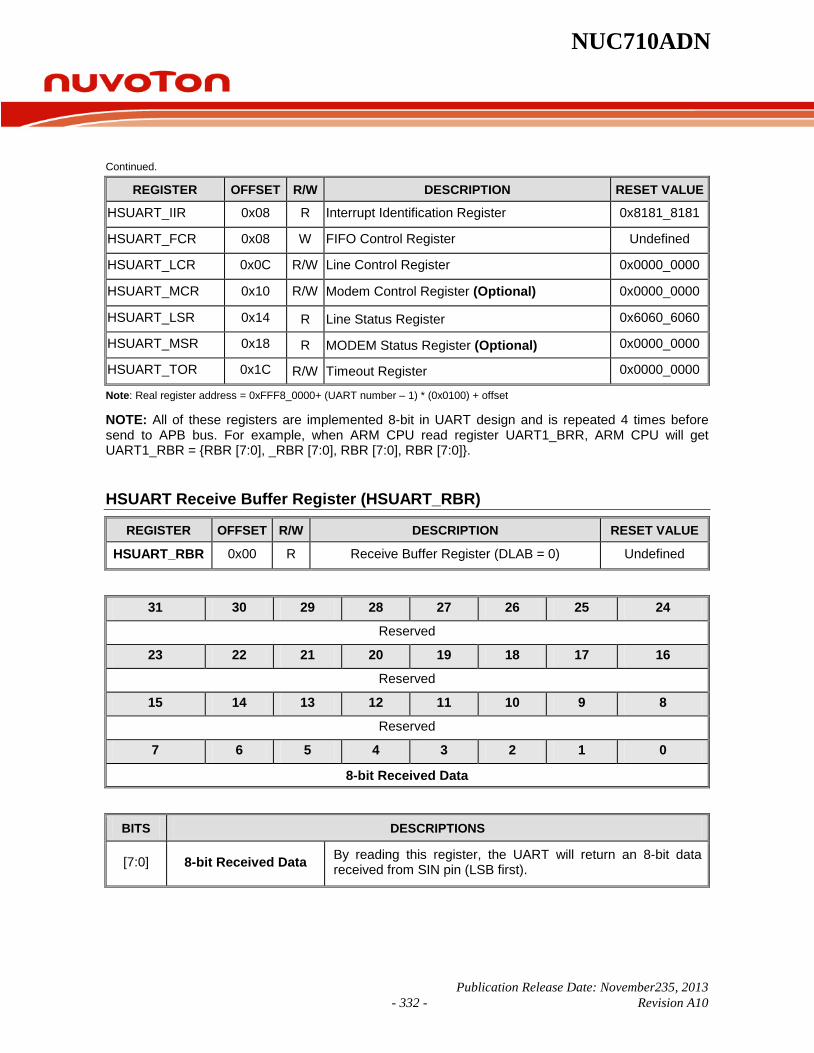
NUC710ADN
Publication Release Date: November235, 2013 - 332 - Revision A10
Continued.
REGISTER OFFSET R/W DESCRIPTION RESET VALUE
HSUART_IIR 0x08 R Interrupt Identification Register 0x8181_8181
HSUART_FCR 0x08 W FIFO Control Register Undefined
HSUART_LCR 0x0C R/W Line Control Register 0x0000_0000
HSUART_MCR 0x10 R/W Modem Control Register (Optional) 0x0000_0000
HSUART_LSR 0x14 R Line Status Register 0x6060_6060
HSUART_MSR 0x18 R MODEM Status Register (Optional) 0x0000_0000
HSUART_TOR 0x1C R/W Timeout Register 0x0000_0000
Note: Real register address = 0xFFF8_0000+ (UART number – 1) * (0x0100) + offset
NOTE: All of these registers are implemented 8-bit in UART design and is repeated 4 times before send to APB bus. For example, when ARM CPU read register UART1_BRR, ARM CPU will get UART1_RBR = RBR [7:0], _RBR [7:0], RBR [7:0], RBR [7:0].
HSUART Receive Buffer Register (HSUART_RBR)
REGISTER OFFSET R/W DESCRIPTION RESET VALUE
HSUART_RBR 0x00 R Receive Buffer Register (DLAB = 0) Undefined
31 30 29 28 27 26 25 24
Reserved
23 22 21 20 19 18 17 16
Reserved
15 14 13 12 11 10 9 8
Reserved
7 6 5 4 3 2 1 0
8-bit Received Data
BITS DESCRIPTIONS
[7:0] 8-bit Received Data By reading this register, the UART will return an 8-bit data received from SIN pin (LSB first).
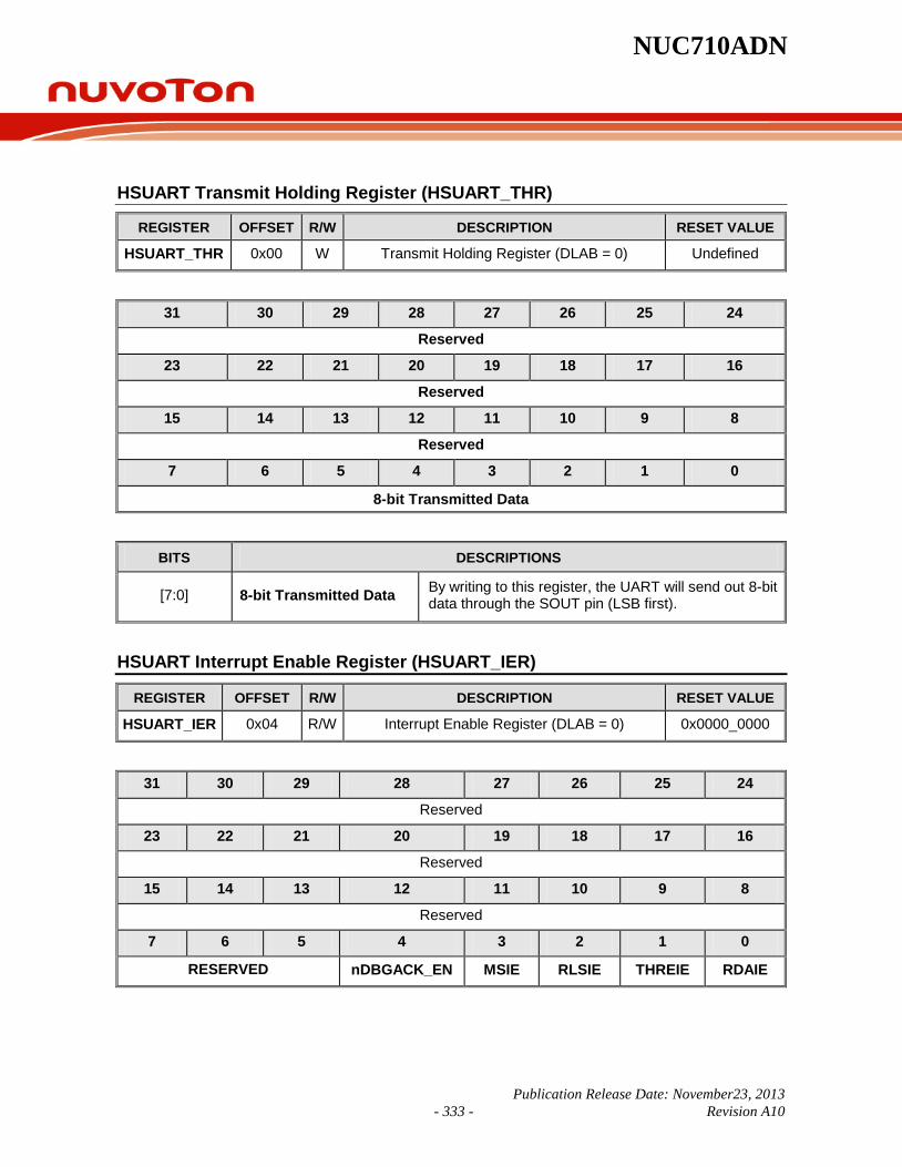
NUC710ADN
Publication Release Date: November23, 2013 - 333 - Revision A10
HSUART Transmit Holding Register (HSUART_THR)
REGISTER OFFSET R/W DESCRIPTION RESET VALUE
HSUART_THR 0x00 W Transmit Holding Register (DLAB = 0) Undefined
31 30 29 28 27 26 25 24
Reserved
23 22 21 20 19 18 17 16
Reserved
15 14 13 12 11 10 9 8
Reserved
7 6 5 4 3 2 1 0
8-bit Transmitted Data
BITS DESCRIPTIONS
[7:0] 8-bit Transmitted Data By writing to this register, the UART will send out 8-bit data through the SOUT pin (LSB first).
HSUART Interrupt Enable Register (HSUART_IER)
REGISTER OFFSET R/W DESCRIPTION RESET VALUE
HSUART_IER 0x04 R/W Interrupt Enable Register (DLAB = 0) 0x0000_0000
31 30 29 28 27 26 25 24
Reserved
23 22 21 20 19 18 17 16
Reserved
15 14 13 12 11 10 9 8
Reserved
7 6 5 4 3 2 1 0
RESERVED nDBGACK_EN MSIE RLSIE THREIE RDAIE

NUC710ADN
Publication Release Date: November235, 2013 - 334 - Revision A10
BITS DESCRIPTIONS
[31:5] Reserved -
[4] nDBGACK_EN
ICE debug mode acknowledge enable 0 = When DBGACK is high, the UART receiver timeout clock is held 1 = Whether the DBGACK is high or not, the UART receiver timerout clock is not held
[3] MSIE MODEM Status Interrupt (Irpt_MOS) Enable 0 = Mask off Irpt_MOS 1 = Enable Irpt_MOS
[2] RLSIE Receive Line Status Interrupt (Irpt_RLS) Enable 0 = Mask off Irpt_RLS 1 = Enable Irpt_RLS
[1] THREIE Transmit Holding Register Empty Interrupt (Irpt_THRE) Enable 0 = Mask off Irpt_THRE 1 = Enable Irpt_THRE
[0] RDAIE
Receive Data Available Interrupt (Irpt_RDA) Enable and Time-out Interrupt (Irpt_TOUT) Enable 0 = Mask off Irpt_RDA and Irpt_TOUT 1 = Enable Irpt_RDA and Irpt_TOUT
HSUART Divider Latch (Low Byte) Register (HSUART_DLL)
REGISTER OFFSET R/W DESCRIPTION RESET VALUE
HSUART_DLL 0x00 R/W Divisor Latch Register (LS) (DLAB = 1) 0x0000_0000
31 30 29 28 27 26 25 24
Reserved
23 22 21 20 19 18 17 16
Reserved
15 14 13 12 11 10 9 8
Reserved
7 6 5 4 3 2 1 0
Baud Rate Divider (Low Byte)
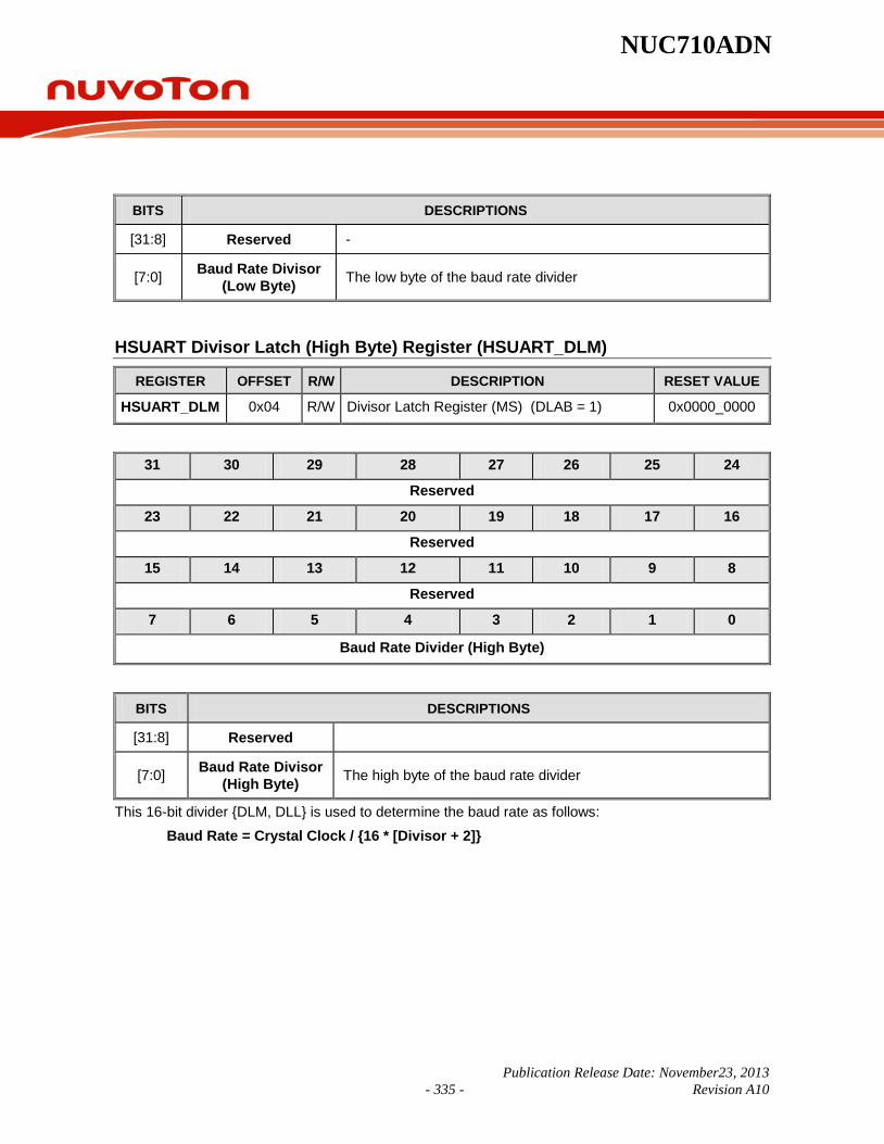
NUC710ADN
Publication Release Date: November23, 2013 - 335 - Revision A10
BITS DESCRIPTIONS
[31:8] Reserved -
[7:0] Baud Rate Divisor (Low Byte) The low byte of the baud rate divider
HSUART Divisor Latch (High Byte) Register (HSUART_DLM)
REGISTER OFFSET R/W DESCRIPTION RESET VALUE
HSUART_DLM 0x04 R/W Divisor Latch Register (MS) (DLAB = 1) 0x0000_0000
31 30 29 28 27 26 25 24
Reserved
23 22 21 20 19 18 17 16
Reserved
15 14 13 12 11 10 9 8
Reserved
7 6 5 4 3 2 1 0
Baud Rate Divider (High Byte)
BITS DESCRIPTIONS
[31:8] Reserved
[7:0] Baud Rate Divisor (High Byte) The high byte of the baud rate divider
This 16-bit divider DLM, DLL is used to determine the baud rate as follows: Baud Rate = Crystal Clock / 16 * [Divisor + 2]
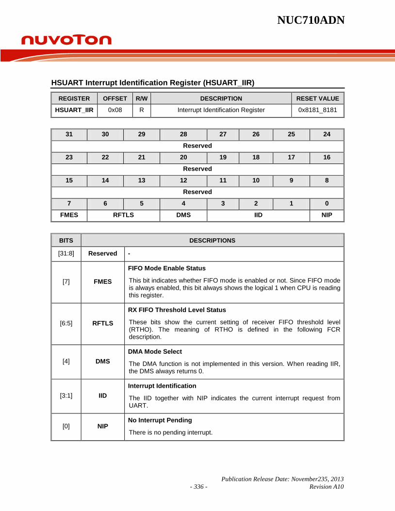
NUC710ADN
Publication Release Date: November235, 2013 - 336 - Revision A10
HSUART Interrupt Identification Register (HSUART_IIR)
REGISTER OFFSET R/W DESCRIPTION RESET VALUE
HSUART_IIR 0x08 R Interrupt Identification Register 0x8181_8181
31 30 29 28 27 26 25 24
Reserved
23 22 21 20 19 18 17 16
Reserved
15 14 13 12 11 10 9 8
Reserved
7 6 5 4 3 2 1 0
FMES RFTLS DMS IID NIP
BITS DESCRIPTIONS
[31:8] Reserved -
[7] FMES
FIFO Mode Enable Status
This bit indicates whether FIFO mode is enabled or not. Since FIFO mode is always enabled, this bit always shows the logical 1 when CPU is reading this register.
[6:5] RFTLS
RX FIFO Threshold Level Status
These bits show the current setting of receiver FIFO threshold level (RTHO). The meaning of RTHO is defined in the following FCR description.
[4] DMS DMA Mode Select
The DMA function is not implemented in this version. When reading IIR, the DMS always returns 0.
[3:1] IID Interrupt Identification
The IID together with NIP indicates the current interrupt request from UART.
[0] NIP No Interrupt Pending
There is no pending interrupt.
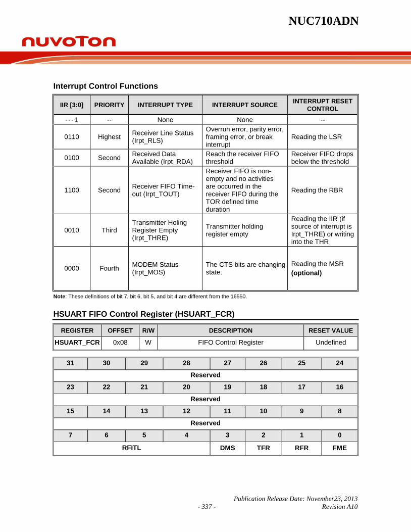
NUC710ADN
Publication Release Date: November23, 2013 - 337 - Revision A10
Interrupt Control Functions
IIR [3:0] PRIORITY INTERRUPT TYPE INTERRUPT SOURCE INTERRUPT RESET CONTROL
- - - 1 -- None None --
0110 Highest Receiver Line Status (Irpt_RLS)
Overrun error, parity error, framing error, or break interrupt
Reading the LSR
0100 Second Received Data Available (Irpt_RDA)
Reach the receiver FIFO threshold
Receiver FIFO drops below the threshold
1100 Second Receiver FIFO Time-out (Irpt_TOUT)
Receiver FIFO is non-empty and no activities are occurred in the receiver FIFO during the TOR defined time duration
Reading the RBR
0010 Third Transmitter Holing Register Empty (Irpt_THRE)
Transmitter holding register empty
Reading the IIR (if source of interrupt is Irpt_THRE) or writing into the THR
0000 Fourth MODEM Status (Irpt_MOS)
The CTS bits are changing state.
Reading the MSR (optional)
Note: These definitions of bit 7, bit 6, bit 5, and bit 4 are different from the 16550.
HSUART FIFO Control Register (HSUART_FCR)
REGISTER OFFSET R/W DESCRIPTION RESET VALUE
HSUART_FCR 0x08 W FIFO Control Register Undefined
31 30 29 28 27 26 25 24
Reserved
23 22 21 20 19 18 17 16
Reserved
15 14 13 12 11 10 9 8
Reserved
7 6 5 4 3 2 1 0
RFITL DMS TFR RFR FME
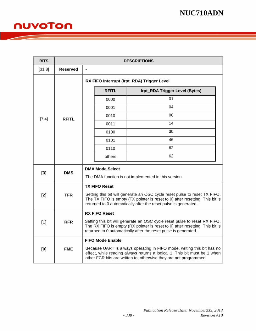
NUC710ADN
Publication Release Date: November235, 2013 - 338 - Revision A10
BITS DESCRIPTIONS
[31:8] Reserved -
[7:4] RFITL
RX FIFO Interrupt (Irpt_RDA) Trigger Level
RFITL Irpt_RDA Trigger Level (Bytes)
0000 01
0001 04
0010 08
0011 14
0100 30
0101 46
0110 62
others 62
[3] DMS DMA Mode Select
The DMA function is not implemented in this version.
[2] TFR
TX FIFO Reset
Setting this bit will generate an OSC cycle reset pulse to reset TX FIFO. The TX FIFO is empty (TX pointer is reset to 0) after resetting. This bit is returned to 0 automatically after the reset pulse is generated.
[1] RFR
RX FIFO Reset
Setting this bit will generate an OSC cycle reset pulse to reset RX FIFO. The RX FIFO is empty (RX pointer is reset to 0) after resetting. This bit is returned to 0 automatically after the reset pulse is generated.
[0] FME
FIFO Mode Enable
Because UART is always operating in FIFO mode, writing this bit has no effect, while reading always returns a logical 1. This bit must be 1 when other FCR bits are written to; otherwise they are not programmed.
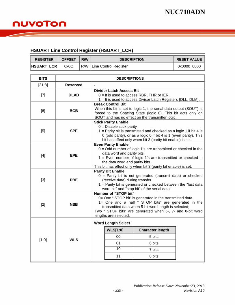
NUC710ADN
Publication Release Date: November23, 2013 - 339 - Revision A10
HSUART Line Control Register (HSUART_LCR)
REGISTER OFFSET R/W DESCRIPTION RESET VALUE
HSUART_LCR 0x0C R/W Line Control Register 0x0000_0000
BITS DESCRIPTIONS
[31:8] Reserved -
[7] DLAB Divider Latch Access Bit
0 = It is used to access RBR, THR or IER. 1 = It is used to access Divisor Latch Registers DLL, DLM.
[6] BCB Break Control Bit When this bit is set to logic 1, the serial data output (SOUT) is forced to the Spacing State (logic 0). This bit acts only on SOUT and has no effect on the transmitter logic.
[5] SPE
Stick Parity Enable 0 = Disable stick parity 1 = Parity bit is transmitted and checked as a logic 1 if bit 4 is
0 (odd parity), or as a logic 0 if bit 4 is 1 (even parity). This bit has effect only when bit 3 (parity bit enable) is set.
[4] EPE
Even Parity Enable 0 = Odd number of logic 1’s are transmitted or checked in the
data word and parity bits. 1 = Even number of logic 1’s are transmitted or checked in
the data word and parity bits. This bit has effect only when bit 3 (parity bit enable) is set.
[3] PBE
Parity Bit Enable 0 = Parity bit is not generated (transmit data) or checked
(receive data) during transfer. 1 = Parity bit is generated or checked between the "last data
word bit" and "stop bit" of the serial data.
[2] NSB
Number of “STOP bit” 0= One “ STOP bit” is generated in the transmitted data 1= One and a half “ STOP bits” are generated in the
transmitted data when 5-bit word length is selected; Two “ STOP bits” are generated when 6-, 7- and 8-bit word lengths are selected.
[1:0] WLS
Word Length Select
WLS[1:0] Character length 00 5 bits
01 6 bits 10 7 bits
11 8 bits

NUC710ADN
Publication Release Date: November235, 2013 - 340 - Revision A10
31 30 29 28 27 26 25 24
Reserved
23 22 21 20 19 18 17 16
Reserved
15 14 13 12 11 10 9 8
Reserved
7 6 5 4 3 2 1 0
DLAB BCB SPE EPE PBE NSB WLS
HSUART Modem Control Register (HSUART_MCR)
REGISTER OFFSET R/W DESCRIPTION RESET VALUE
HSUART_MCR 0x10 R/W Modem Control Register (Optional) 0x0000_0000
31 30 29 28 27 26 25 24
Reserved
23 22 21 20 19 18 17 16
Reserved
15 14 13 12 11 10 9 8
Reserved
7 6 5 4 3 2 1 0
Reserved LBME Reserved RTS Reserved
BITS DESCRIPTIONS
[31:5] Reserved -
[4] LBME
Loop-back Mode Enable 0 = Disable 1 = When loop-back mode is enabled, the following signals are connected internally: SOUT connected to SIN and SOUT pin fixed at logic 1 RTS# connected to CTS# and RTS# pin fixed at logic 1
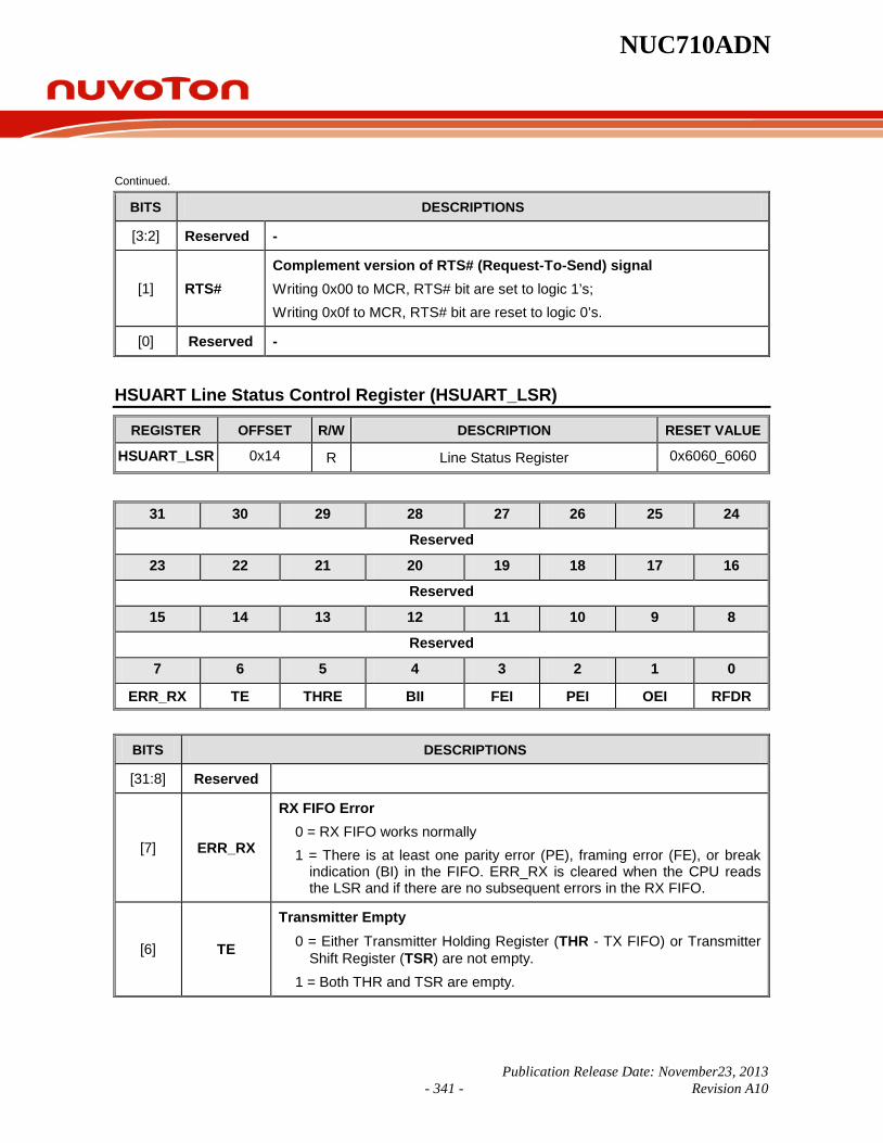
NUC710ADN
Publication Release Date: November23, 2013 - 341 - Revision A10
Continued.
BITS DESCRIPTIONS
[3:2] Reserved -
[1] RTS# Complement version of RTS# (Request-To-Send) signal Writing 0x00 to MCR, RTS# bit are set to logic 1’s; Writing 0x0f to MCR, RTS# bit are reset to logic 0’s.
[0] Reserved -
HSUART Line Status Control Register (HSUART_LSR)
REGISTER OFFSET R/W DESCRIPTION RESET VALUE
HSUART_LSR 0x14 R Line Status Register 0x6060_6060
31 30 29 28 27 26 25 24
Reserved
23 22 21 20 19 18 17 16
Reserved
15 14 13 12 11 10 9 8
Reserved
7 6 5 4 3 2 1 0
ERR_RX TE THRE BII FEI PEI OEI RFDR
BITS DESCRIPTIONS
[31:8] Reserved
[7] ERR_RX
RX FIFO Error 0 = RX FIFO works normally 1 = There is at least one parity error (PE), framing error (FE), or break
indication (BI) in the FIFO. ERR_RX is cleared when the CPU reads the LSR and if there are no subsequent errors in the RX FIFO.
[6] TE
Transmitter Empty 0 = Either Transmitter Holding Register (THR - TX FIFO) or Transmitter
Shift Register (TSR) are not empty. 1 = Both THR and TSR are empty.

NUC710ADN
Publication Release Date: November235, 2013 - 342 - Revision A10
Continued.
BITS DESCRIPTIONS
[5] THRE
Transmitter Holding Register Empty 0 = THR is not empty. 1 = THR is empty.
THRE is set when the last data word of TX FIFO is transferred to Transmitter Shift Register (TSR). The CPU resets this bit when the THR (or TX FIFO) is loaded. This bit also causes the UART to issue an interrupt (Irpt_THRE) to the CPU when IER [1]=1.
[4] BII
Break Interrupt Indicator This bit is set to logic 1 whenever the received data input is held in the "spacing state" (logic 0) for longer than a full word transmission time (that is, the total time of "start bit" + data bits + parity + stop bits) and is reset whenever the CPU reads the contents of the LSR.
[3] FEI
Framing Error Indicator
This bit is set to logic 1 whenever the received character does not have a valid "stop bit" (that is, the stop bit following the last data bit or parity bit is detected as a logic 0), and is reset whenever the CPU reads the contents of the LSR.
[2] PEI
Parity Error Indicator
This bit is set to logic 1 whenever the received character does not have a valid "parity bit", and is reset whenever the CPU reads the contents of the LSR.
[1] OEI
Overrun Error Indicator
An overrun error occurs only after the RX FIFO is full and the next character has been completely received in the shift register. The character in the shift register is overwritten, but it is not transferred to the RX FIFO. OE is indicated to the CPU as soon as it happens and is reset whenever the CPU reads the contents of the LSR.
[0] RFDR
RX FIFO Data Ready
0 = RX FIFO is empty
1 = RX FIFO contains at least 1 received data word.
LSR [4:2] (BII, FEI, PEI) are revealed to the CPU when its associated character is at the top of the RX FIFO. These three error indicators are reset whenever the CPU reads the contents of the LSR. LSR [4:1] (BII, FEI, PEI, OEI) are the error conditions that produce a "receiver line status interrupt" (Irpt_RLS) when IER [2]=1. Reading LSR clears Irpt_RLS. Writing LSR is a null operation (not suggested).

NUC710ADN
Publication Release Date: November23, 2013 - 343 - Revision A10
HSUART Modem Status Register (HSUART_MSR)
REGISTER OFFSET R/W DESCRIPTION RESET VALUE
HSUART_MSR 0x18 R MODEM Status Register (Optional) 0x0000_0000
31 30 29 28 27 26 25 24
Reserved
23 22 21 20 19 18 17 16
Reserved
15 14 13 12 11 10 9 8
Reserved
7 6 5 4 3 2 1 0
Reserved CTS# Reserved DCTS
BITS DESCRIPTIONS
[31:5] Reserved -
[4] CTS# Complement version of clear to send (CTS#) input (This bit is selected by IP)
[3:1] Reserved -
[0] DCTS
CTS# State Change (This bit is selected by IP) This bit is set whenever CTS# input has changed state, and is reset if the CPU reads the MSR.
Whenever any MSR [0] is set to logic 1, a Modem Status Interrupt is generated if IER[3]=1. Writing to the MSR is a null operation (not recommended).

NUC710ADN
Publication Release Date: November235, 2013 - 344 - Revision A10
HSUART Time Out Register (HSUART_TOR)
REGISTER OFFSET R/W DESCRIPTION RESET VALUE
HSUART_TOR 0x1C R/W Time Out Register 0x0000_0000
31 30 29 28 27 26 25 24
Reserved
23 22 21 20 19 18 17 16
Reserved
15 14 13 12 11 10 9 8
Reserved
7 6 5 4 3 2 1 0
TOIE TOIC
BITS DESCRIPTIONS
[31:8] Reserved -
[7] TOIE Time Out Interrupt Enable The receiver timeout interrupt is enabled only when TOR [7] = IER[0] = 1.
[6:0] TOIC
Time Out Interrupt Comparator The time out counter resets and starts counting (the counting clock = baud rate) whenever the RX FIFO receives a new data word. Once the content of the timeout counter (TOUT_CNT) is equal to that of the timeout interrupt comparator (TOIC), a receiver time out interrupt (Irpt_TOUT) is generated if TOR [7] = IER [0] = 1. A new incoming data word or RX FIFO empty clears Irpt_TOUT.

NUC710ADN
Publication Release Date: November23, 2013 - 345 - Revision A10
6.13 Timer/Watchdog Controller 6.13.1 General Timer Controller The timer module includes two channels, TIMER0 and TIMER1, which allows you to easily implement a counting scheme. The timer can perform functions like frequency measurement, event counting, interval measurement, clock generation, delay timing, and so on. The timer possesses features such as adjustable resolution, programmable counting period, and detailed information. The timer can generate an interrupt signal upon timeout, or provide the current value of count during operation. The general TIMER Controller includes the following features AMBA APB interface compatible Two channels with an 8-bit presale counter/24-bit down counter and an interrupt request each Independent clock source for each channel Maximum uninterrupted time = (1 / 25 MHz) * (256) * (2^24), if TCLK = 25 MHz
6.13.2 Watchdog Timer
6.13.3 Timer Control Registers Map R: read only, W: write only, R/W: both read and write
REGISTER ADDRESS R/W/C DESCRIPTION RESET VALUE
TCSR0 0xFFF8_1000 R/W Timer Control and Status Register 0 0x0000_0005
TCSR1 0xFFF8_1004 R/W Timer Control and Status Register 1 0x0000_0005
TICR0 0xFFF8_1008 R/W Timer Initial Control Register 0 0x0000_0000
TICR1 0xFFF8_100C R/W Timer Initial Control Register 1 0x0000_0000
TDR0 0xFFF8_1010 R Timer Data Register 0 0x0000_0000
TDR1 0xFFF8_1014 R Timer Data Register 1 0x0000_0000
TISR 0xFFF8_1018 R/W Timer Interrupt Status Register 0x0000_0000
WTCR 0xFFF8_101C R/W Watchdog Timer Control Register 0x0000_0400
Timer Control Register 0/1 (TCSR 0/1)
REGISTER ADDRESS R/W DESCRIPTION RESET VALUE
TCSR0 0xFFF8_1000 R/W Timer Control and Status Register 0 0x0000_0005
TCSR1 0xFFF8_1004 R/W Timer Control and Status Register 1 0x0000_0005
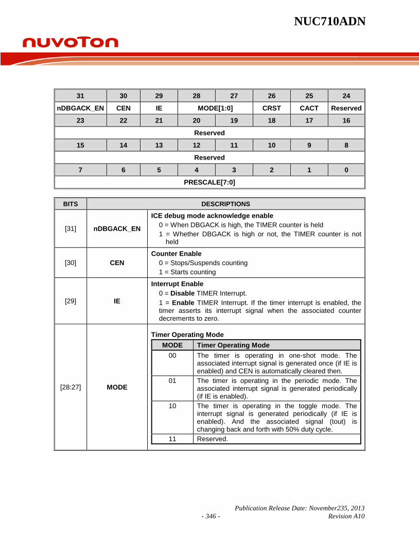
NUC710ADN
Publication Release Date: November235, 2013 - 346 - Revision A10
31 30 29 28 27 26 25 24
nDBGACK_EN CEN IE MODE[1:0] CRST CACT Reserved
23 22 21 20 19 18 17 16
Reserved
15 14 13 12 11 10 9 8
Reserved
7 6 5 4 3 2 1 0
PRESCALE[7:0]
BITS DESCRIPTIONS
[31] nDBGACK_EN
ICE debug mode acknowledge enable 0 = When DBGACK is high, the TIMER counter is held 1 = Whether DBGACK is high or not, the TIMER counter is not
held
[30] CEN Counter Enable
0 = Stops/Suspends counting 1 = Starts counting
[29] IE
Interrupt Enable 0 = Disable TIMER Interrupt. 1 = Enable TIMER Interrupt. If the timer interrupt is enabled, the timer asserts its interrupt signal when the associated counter decrements to zero.
[28:27] MODE
Timer Operating Mode MODE Timer Operating Mode
00 The timer is operating in one-shot mode. The associated interrupt signal is generated once (if IE is enabled) and CEN is automatically cleared then.
01 The timer is operating in the periodic mode. The associated interrupt signal is generated periodically (if IE is enabled).
10 The timer is operating in the toggle mode. The interrupt signal is generated periodically (if IE is enabled). And the associated signal (tout) is changing back and forth with 50% duty cycle.
11 Reserved.
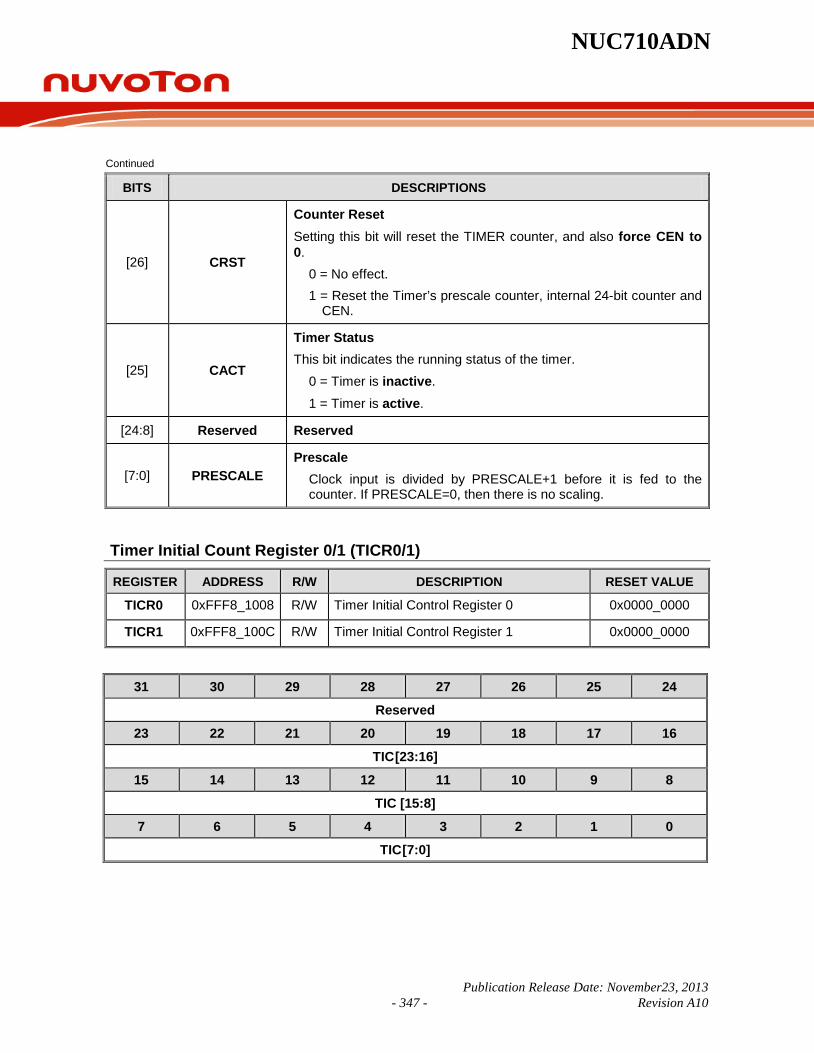
NUC710ADN
Publication Release Date: November23, 2013 - 347 - Revision A10
Continued
BITS DESCRIPTIONS
[26] CRST
Counter Reset Setting this bit will reset the TIMER counter, and also force CEN to 0.
0 = No effect. 1 = Reset the Timer’s prescale counter, internal 24-bit counter and
CEN.
[25] CACT
Timer Status This bit indicates the running status of the timer.
0 = Timer is inactive.
1 = Timer is active.
[24:8] Reserved Reserved
[7:0] PRESCALE Prescale
Clock input is divided by PRESCALE+1 before it is fed to the counter. If PRESCALE=0, then there is no scaling.
Timer Initial Count Register 0/1 (TICR0/1)
REGISTER ADDRESS R/W DESCRIPTION RESET VALUE
TICR0 0xFFF8_1008 R/W Timer Initial Control Register 0 0x0000_0000
TICR1 0xFFF8_100C R/W Timer Initial Control Register 1 0x0000_0000
31 30 29 28 27 26 25 24
Reserved
23 22 21 20 19 18 17 16
TIC [23:16]
15 14 13 12 11 10 9 8
TIC [15:8]
7 6 5 4 3 2 1 0
TIC [7:0]

NUC710ADN
Publication Release Date: November235, 2013 - 348 - Revision A10
BITS DESCRIPTIONS
[31:24] Reserved Reserved
[23:0] TIC
Timer Initial Count This is a 24-bit value representing the initial count. The timer will reload this value whenever the counter is decremented to zero.
NOTE1: Never write 0x0 in the TIC, or the core will run into an unknown state. NOTE2: Regardless of whether CEN is 0 or 1, whenever the software writes a new value to this register, the TIMER aborts the previous count and restarts using the new value.
Timer Data Register 0/1 (TDR0/1)
REGISTER ADDRESS R/W DESCRIPTION RESET VALUE
TDR0 0xFFF8_1010 R Timer Data Register 0 0x0000_0000
TDR1 0xFFF8_1014 R Timer Data Register 1 0x0000_0000
31 30 29 28 27 26 25 24
Reserved
23 22 21 20 19 18 17 16
TDR [23:16]
15 14 13 12 11 10 9 8
TDR [15:8]
7 6 5 4 3 2 1 0
TDR [7:0]
BITS DESCRIPTIONS
[31:24] Reserved Reserved
[23:0] TDR
Timer Data Register The current count is registered in this 24-bit value. NOTE: Software can read the current value on this register only when CEN = 0, or the value represented here is not a correct one.

NUC710ADN
Publication Release Date: November23, 2013 - 349 - Revision A10
Timer Interrupt Status Register (TISR)
REGISTER ADDRESS R/W DESCRIPTION RESET VALUE
TISR 0xFFF8_1018 R/W Timer Interrupt Status Register 0x0000_0000
31 30 29 28 27 26 25 24
Reserved
23 22 21 20 19 18 17 16
Reserved
15 14 13 12 11 10 9 8
Reserved
7 6 5 4 3 2 1 0
Reserved TIF1 TIF0
BITS DESCRIPTIONS
[1] TIF1
Timer Interrupt Flag 1 This bit indicates the interrupt status of Timer channel 1. 0 = Indicates that Timer 1 has not reached zero. 1 = Indicates Timer 1 reached zero. If enabled, the interrupt flag is set. NOTE: This bit is read only, but can be cleared by writing 1.
[0] TIF0
Timer Interrupt Flag 0 This bit indicates the interrupt status of Timer channel 0. 0 = Indicates that Timer 0 has not reached zero. 1 = Indicates Timer 0 reached zero. If enabled, the interrupt flag is set. NOTE: This bit is read only, but can be cleared by writing 0.
Watchdog Timer Control Register (WTCR)
REGISTER ADDRESS R/W DESCRIPTION RESET VALUE
WTCR 0xFFF8_101C R/W Watchdog Timer Control Register 0x0000_0400

NUC710ADN
Publication Release Date: November235, 2013 - 350 - Revision A10
31 30 29 28 27 26 25 24
Reserved
23 22 21 20 19 18 17 16
Reserved
15 14 13 12 11 10 9 8
Reserved WTCLK nDBGACK_EN WTTME
7 6 5 4 3 2 1 0
WTE WTIE WTIS WTIF WTRF WTRE WTR
BITS DESCRIPTIONS
[31:11] Reserved Reserved
[10] WTCLK
Watchdog Timer Use this bit to divide the Watchdog Timer clock source by 256. The Watchdog Timer clock source is Crystal input.
0 = Uses original clock input 1 = Clock input is divided by 256
NOTE: When WTTME = 1, setting this bit has no effect on the WDT clock (using original clock input).
[9] nDBGACK_EN
ICE debug mode acknowledge enable 0 = When DBGACK is high, the Watchdog Timer counter is held 1 = Whether DBGACK is high or not, the Watchdog Timer counter
is not held
[8] WTTME
Watchdog Timer Test Mode Enable For reasons of efficiency, the 26-bit counter within the Watchdog Timer is considered as two independent 13-bit counters in test mode. They are operated concurrently and separately during the test. This approach can save a lot of time spent testing. When the 13-bit counter overflows, a Watchdog Timer interrupt is generated.
0 = Watchdog Timer operates in normal mode 1 = Watchdog Timer operates in test mode
[7] WTE
Watchdog Timer Enable 0 = Disable the Watchdog Timer (this action will reset the internal
counter) 1 = Enable the Watchdog Timer

NUC710ADN
Publication Release Date: November23, 2013 - 351 - Revision A10
Continued
BITS DESCRIPTIONS
[6] WTIE Watchdog Timer Interrupt Enable
0 = Disable the Watchdog Timer interrupt 1 = Enable the Watchdog Timer interrupt
[5:4] WTIS
Watchdog Timer Interval Select These two bits select the interval for the Watchdog Timer. No matter which interval is chosen, the timeout reset always occurs 512 WDT clock cycles later than the interrupt timeout.
WTIS Interrupt Timeout Reset Timeout Real Time Interval
(CLK=15MHz/256)
00 214 clocks 214 + 1024 clocks
0.28 sec.
01 216 clocks 216 + 1024 clocks
1.12 sec.
10 218 clocks 218 + 1024 clocks
4.47 sec.
11 220 clocks 220 + 1024 clocks
17.9 sec.
[3] WTIF
Watchdog Timer Interrupt Flag If the Watchdog Timer interrupt is enabled, then the hardware sets this bit to indicate that a Watchdog Timer interrupt occurred. If the Watchdog Timer interrupt is not enabled, this bit indicates that a timeout period has elapsed.
0 = Watchdog Timer interrupt did not occur 1 = Watchdog Timer interrupt occurred
NOTE: This bit is read only, but can be cleared by writing 1.
[2] WTRF
Watchdog Timer Reset Flag When the Watchdog Timer initiates a reset, the hardware will set this bit. This flag can be read by software to determine the source of the reset. This flag is not self-clearing, and must be cleared by the programmer. If WTRE is disabled, then the Watchdog Timer has no effect on this bit.
0 = Watchdog Timer reset does not occur 1 = Watchdog Timer reset occurs
NOTE: This bit is read only, but can be cleared by writing 1.
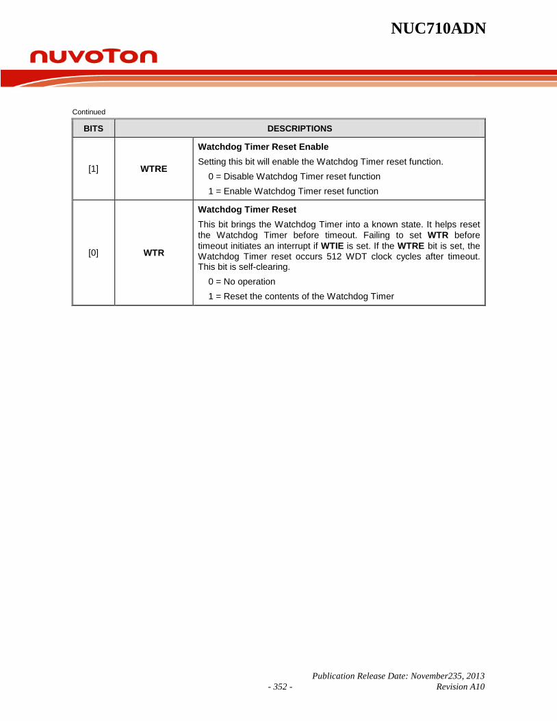
NUC710ADN
Publication Release Date: November235, 2013 - 352 - Revision A10
Continued
BITS DESCRIPTIONS
[1] WTRE
Watchdog Timer Reset Enable Setting this bit will enable the Watchdog Timer reset function.
0 = Disable Watchdog Timer reset function 1 = Enable Watchdog Timer reset function
[0] WTR
Watchdog Timer Reset This bit brings the Watchdog Timer into a known state. It helps reset the Watchdog Timer before timeout. Failing to set WTR before timeout initiates an interrupt if WTIE is set. If the WTRE bit is set, the Watchdog Timer reset occurs 512 WDT clock cycles after timeout. This bit is self-clearing.
0 = No operation 1 = Reset the contents of the Watchdog Timer

NUC710ADN
Publication Release Date: November23, 2013 - 353 - Revision A10
6.14 Advanced Interrupt Controller An interrupt temporarily changes the sequence of program execution to react to a particular event such as power failure, watchdog timer timeout, transmit/receive requests from the Ethernet MAC Controller, and so on. The ARM7TDMI processor provides two modes of interrupt, the Fast Interrupt (FIQ) mode for critical sessions and the Interrupt (IRQ) mode for general purpose. An IRQ exception occurs when the nIRQ input is asserted. Similarly, an FIQ exception occurs when the nFIQ input is asserted. The FIQ has privilege over the IRQ and can preempt an ongoing IRQ. It is possible to ignore the FIQ and the IRQ by setting the F and I bits in the current program status register (CPSR). NUC710 incorporates an advanced interrupt controller (AIC) capable of dealing with interrupt requests from a total of 32 different sources. Currently, 31 interrupt sources are defined. Each interrupt source is uniquely assigned an interrupt channel. For example, the watchdog timer interrupt is assigned to channel 1. The AIC implements a proprietary eight-level priority scheme that differentiates the available 31 interrupt sources into eight priority levels. Interrupt sources within priority level 0 have the highest priority and the priority level 7 has the lowest. To work this scheme properly, you must specify a certain priority level to each interrupt source during power-on initialization; otherwise, the system shall behave unexpectedly. Within each priority level, interrupt source that is positioned in a lower channel has a higher priority. Interrupt source that is active, enabled, and positioned in the lowest channel within the priority level 0 is promoted to the FIQ. Interrupt sources within the priority levels other than 0 can petition for the IRQ. The IRQ can be preempted by the occurrence of the FIQ. Interrupt nesting is performed automatically by the AIC. Though interrupt sources originating from the NUC710 itself are intrinsically high-level sensitive, the AIC can be configured as either low-level sensitive, high-level sensitive, negative-edge triggered, or positive-edge triggered to each interrupt source. When the NUC710 is put in test mode, all interrupt sources must be configured as positive-edge triggered. The advanced interrupt controller includes the following features: AMBA APB bus interface External interrupts can be programmed as either edge-triggered or level-sensitive External interrupts can be programmed as either low-active or high-active Has flags to reflect the status of each interrupt source Individual mask for each interrupt source Proprietary 8-level interrupt scheme to ease the burden from the interrupt Priority methodology is adopted to allow for interrupt daisy-chaining Automatically masking out lower priority interrupts during interrupt nesting Automatically clears the interrupt flag when an external interrupt source is programmed to be edge-
triggered
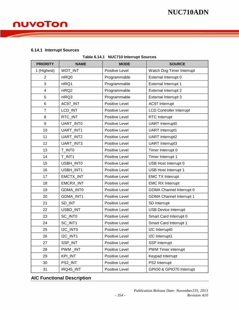
NUC710ADN
Publication Release Date: November235, 2013 - 354 - Revision A10
6.14.1 Interrupt Sources Table 6.14.1 NUC710 Interrupt Sources
PRIORITY NAME MODE SOURCE
1 (Highest) WDT_INT Positive Level Watch Dog Timer Interrupt
2 nIRQ0 Programmable External Interrupt 0
3 nIRQ1 Programmable External Interrupt 1
4 nIRQ2 Programmable External Interrupt 2
5 nIRQ3 Programmable External Interrupt 3
6 AC97_INT Positive Level AC97 Interrupt
7 LCD_INT Positive Level LCD Controller Interrupt
8 RTC_INT Positive Level RTC Interrupt
9 UART_INT0 Positive Level UART Interrupt0
10 UART_INT1 Positive Level UART Interrupt1
11 UART_INT2 Positive Level UART Interrupt2
12 UART_INT3 Positive Level UART Interrupt3
13 T_INT0 Positive Level Timer Interrupt 0
14 T_INT1 Positive Level Timer Interrupt 1
15 USBH_INT0 Positive Level USB Host Interrupt 0
16 USBH_INT1 Positive Level USB Host Interrupt 1
17 EMCTX_INT Positive Level EMC TX Interrupt
18 EMCRX_INT Positive Level EMC RX Interrupt
19 GDMA_INT0 Positive Level GDMA Channel Interrupt 0
20 GDMA_INT1 Positive Level GDMA Channel Interrupt 1
21 SD_INT Positive Level SD Interrupt
22 USBD_INT Positive Level USB Device Interrupt
23 SC_INT0 Positive Level Smart Card Interrupt 0
24 SC_INT1 Positive Level Smart Card Interrupt 1
25 I2C_INT0 Positive Level I2C Interrupt0
26 I2C_INT1 Positive Level I2C Interrupt1
27 SSP_INT Positive Level SSP Interrupt
28 PWM _INT Positive Level PWM Timer interrupt
29 KPI_INT Positive Level Keypad Interrupt
30 PS2_INT Positive Level PS2 Interrupt
31 IRQ45_INT Positive Level GPIO0 & GPIO70 Interrupt
AIC Functional Description
NUC710ADN
Publication Release Date: November23, 2013 - 355 - Revision A10
Hardware Interrupt Vectoring Hardware interrupt vectoring can be used to shorten the interrupt latency. If not used, priority determination must be carried out by software. When the Interrupt Priority Encoding Register (AIC_IPER) is read, it will return an integer representing the channel that is active and having the highest priority. This integer is equivalent to multiplication by 4 (shifted left two bits to word-align it) such that it may be used directly to index into a branch table to select the appropriate interrupt service routine vector. Priority Controller An 8-level priority encoder controls the NIRQ line. Each interrupt source belongs to a priority group between 0 and 7. Group 0 has the highest priority and group 7, the lowest. When more than one unmasked interrupt channels are active at a time, the interrupt with the highest priority is serviced first. If all active interrupts have equal priority, the interrupt with the lowest interrupt source number is serviced first. The current priority level is defined as the priority level of the interrupt with the highest priority at the time the register AIC_IPER is read. In the event that a higher priority unmasked interrupt occurs while an interrupt already exits, there are two possible outcomes depending on whether the AIC_IPER has been read. If the processor has already read the AIC_IPER and caused the NIRQ line to be deasserted, then the NIRQ line is reasserted. When the processor has enabled nested interrupts and reads the AIC_IPER again, it reads the new, higher priority interrupt vector. At the same time, the current priority level is updated to a higher priority. If the AIC_IPER has not been read after the NIRQ line has been asserted, then the processor will read the new higher priority interrupt vector in the AIC_IPER register and the current priority level is updated. When the End of Service Command Register (AIC_EOSCR) is written, the current interrupt level is updated with the last stored interrupt level from the stack (if any). Therefore, at the end of a higher priority interrupt, the AIC returns to the previous state corresponding to the preceding lower priority interrupt which was interrupted. Interrupt Handling When the IRQ line is asserted, the interrupt handler must read the AIC_IPER as soon as possible. This can deassert the NIRQ request to the processor and clears the interrupt if it is programmed to be edge triggered. This allows the AIC to assert the NIRQ line again when a higher priority unmasked interrupt occurs. The AIC_EOSCR (End of Service Command Register) must be written at the end of the interrupt service routine. This permits pending interrupts to be serviced.

NUC710ADN
Publication Release Date: November235, 2013 - 356 - Revision A10
Interrupt Masking Each interrupt source, including FIQ, can be enabled or disabled individually by using command registers AIC_MECR and AIC_MDCR. The status of the interrupt mask can be read in the read only register AIC_IMR. A disabled interrupt doesn’t affect the servicing of other interrupts. Interrupt Clearing and Setting All interrupt sources (including FIQ) can be individually set or clear by respectively writing to the registers AIC_SSCR and AIC_SCCR when they are programmed to be edge triggered. This feature of the AIC is useful in auto-testing or software debugging. Fake Interrupt When the AIC asserts the NIRQ line, the processor enters interrupt mode and the interrupt handler reads the AIC_IPER, it may happen that AIC deasserts the NIRQ line after the processor has taken into account the NIRQ assertion and before the read of the AIC_IPER. This behavior is called a fake interrupt. The AIC is able to detect these fake interrupts and returns all zero when AIC_IPER is read. The same mechanism of fake interrupt occurs if the processor reads the AIC_IPER (application software or ICE) when there is no interrupt pending. The current priority level is not updated in this situation. Hence, the AIC_EOSCR shouldn’t be written. ICE/Debug Mode This mode allows reading of the AIC_IPER without performing the associated automatic operations. This is necessary when working with a debug system. When an ICE or debug monitor reads the AIC user interface, the AIC_IPER can be read. This has the following consequences in normal mode:
If there is no enabled pending interrupt, the fake vector is returned. If an enabled interrupt with a higher priority than the current one is pending, it is stacked.
In the second case, an End-of-Service command is necessary to restore the state of the AIC. This operation is generally not performed by the debug system. Therefore, the debug system would become strongly intrusive, and may cause the application to enter an undesired state. This can be avoided by using ICE/Debug Mode. When this mode is enabled. The AIC performs interrupt stacking only when write access is performed on the AIC_IPER. Hence, the interrupt service routine must write to the AIC_IPER (any value) just after reading it. When AIC_IPER is written, the new status of AIC, including the value of interrupt source number register (AIC_ISNR), is updated with the value that is kept at the previous AIC_IPER. The debug system must not write to the AIC_IPER as this would cause undesirable effects. The following table shows the main steps of an interrupt and the order in which they are performed according to the mode:

NUC710ADN
Publication Release Date: November23, 2013 - 357 - Revision A10
ACTION NORMAL MODE ICE/DEBUG MODE
Calculate active interrupt Read AIC_IPER Read AIC_IPER
Determine and return the vector of the active interrupt Read AIC_IPER Read AIC_IPER
Push on internal stack the current priority level Read AIC_IPER Write AIC_IPER
Acknowledge the interrupt (Note 1) Read AIC_IPER Write AIC_IPER
No effect (Note 2) Read AIC_IPER
Notes: NIRQ deassertion and automatic interrupt clearing if the source is programmed as level
sensitive. Note that software which has been written and debugged using this mode will run correctly in
normal mode without modification. However, in normal mode writing to AIC_IPER has no effect and can be removed to optimize the code
6.14.2 AIC Registers Map
REGISTER ADDRESS R/W DESCRIPTION RESET VALUE
AIC_SCR1 0xFFF8_2004 R/W Source Control Register 1 0x0000_0047
AIC_SCR2 0xFFF8_2008 R/W Source Control Register 2 0x0000_0047
AIC_SCR3 0xFFF8_200C R/W Source Control Register 3 0x0000_0047
AIC_SCR4 0xFFF8_2010 R/W Source Control Register 4 0x0000_0047
AIC_SCR5 0xFFF8_2014 R/W Source Control Register 5 0x0000_0047
AIC_SCR6 0xFFF8_2018 R/W Source Control Register 6 0x0000_0047
AIC_SCR7 0xFFF8_201C R/W Source Control Register 7 0x0000_0047
AIC_SCR8 0xFFF8_2020 R/W Source Control Register 8 0x0000_0047
AIC_SCR9 0xFFF8_2024 R/W Source Control Register 9 0x0000_0047
AIC_SCR10 0xFFF8_2028 R/W Source Control Register 10 0x0000_0047
AIC_SCR11 0xFFF8_202C R/W Source Control Register 11 0x0000_0047
AIC_SCR12 0xFFF8_2030 R/W Source Control Register 12 0x0000_0047
AIC_SCR13 0xFFF8_2034 R/W Source Control Register 13 0x0000_0047
AIC_SCR14 0xFFF8_2038 R/W Source Control Register 14 0x0000_0047
AIC_SCR15 0xFFF8_203C R/W Source Control Register 15 0x0000_0047
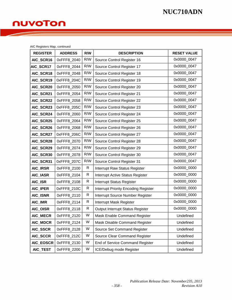
NUC710ADN
Publication Release Date: November235, 2013 - 358 - Revision A10
AIC Registers Map, continued
REGISTER ADDRESS R/W DESCRIPTION RESET VALUE
AIC_SCR16 0xFFF8_2040 R/W Source Control Register 16 0x0000_0047
AIC_SCR17 0xFFF8_2044 R/W Source Control Register 17 0x0000_0047
AIC_SCR18 0xFFF8_2048 R/W Source Control Register 18 0x0000_0047
AIC_SCR19 0xFFF8_204C R/W Source Control Register 19 0x0000_0047
AIC_SCR20 0xFFF8_2050 R/W Source Control Register 20 0x0000_0047
AIC_SCR21 0xFFF8_2054 R/W Source Control Register 21 0x0000_0047
AIC_SCR22 0xFFF8_2058 R/W Source Control Register 22 0x0000_0047
AIC_SCR23 0xFFF8_205C R/W Source Control Register 23 0x0000_0047
AIC_SCR24 0xFFF8_2060 R/W Source Control Register 24 0x0000_0047
AIC_SCR25 0xFFF8_2064 R/W Source Control Register 25 0x0000_0047
AIC_SCR26 0xFFF8_2068 R/W Source Control Register 26 0x0000_0047
AIC_SCR27 0xFFF8_206C R/W Source Control Register 27 0x0000_0047
AIC_SCR28 0xFFF8_2070 R/W Source Control Register 28 0x0000_0047
AIC_SCR29 0xFFF8_2074 R/W Source Control Register 29 0x0000_0047
AIC_SCR30 0xFFF8_2078 R/W Source Control Register 30 0x0000_0047
AIC_SCR31 0xFFF8_207C R/W Source Control Register 31 0x0000_0047
AIC_IRSR 0xFFF8_2100 R Interrupt Raw Status Register 0x0000_0000
AIC_IASR 0xFFF8_2104 R Interrupt Active Status Register 0x0000_0000
AIC_ISR 0xFFF8_2108 R Interrupt Status Register 0x0000_0000
AIC_IPER 0xFFF8_210C R Interrupt Priority Encoding Register 0x0000_0000
AIC_ISNR 0xFFF8_2110 R Interrupt Source Number Register 0x0000_0000
AIC_IMR 0xFFF8_2114 R Interrupt Mask Register 0x0000_0000
AIC_OISR 0xFFF8_2118 R Output Interrupt Status Register 0x0000_0000
AIC_MECR 0xFFF8_2120 W Mask Enable Command Register Undefined
AIC_MDCR 0xFFF8_2124 W Mask Disable Command Register Undefined
AIC_SSCR 0xFFF8_2128 W Source Set Command Register Undefined
AIC_SCCR 0xFFF8_212C W Source Clear Command Register Undefined
AIC_EOSCR 0xFFF8_2130 W End of Service Command Register Undefined
AIC_TEST 0xFFF8_2200 W ICE/Debug mode Register Undefined
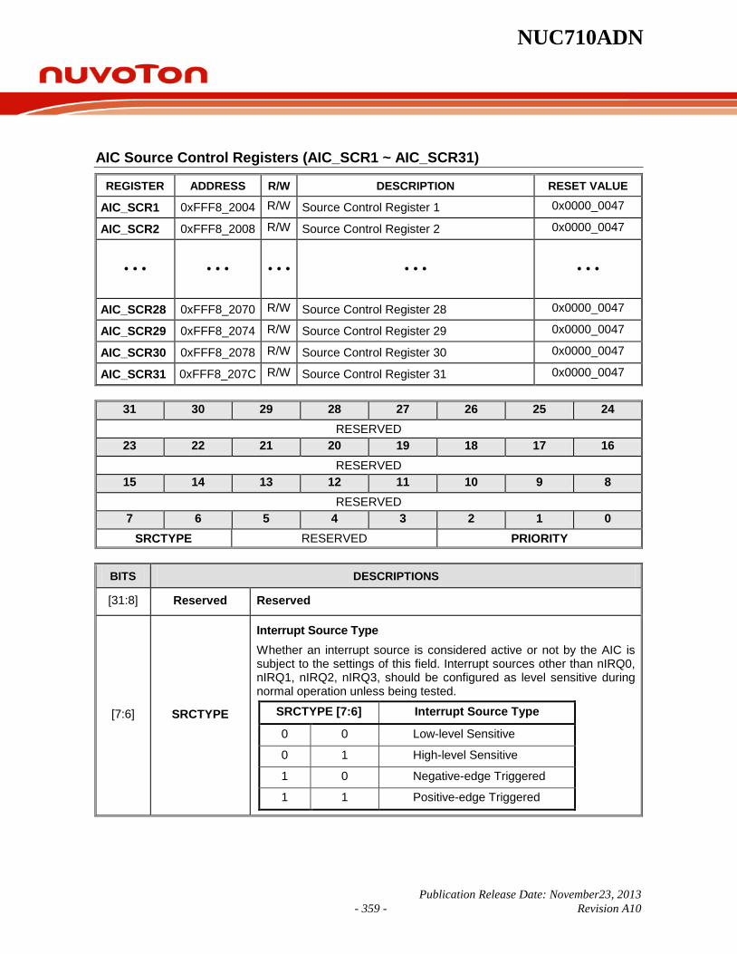
NUC710ADN
Publication Release Date: November23, 2013 - 359 - Revision A10
AIC Source Control Registers (AIC_SCR1 ~ AIC_SCR31)
REGISTER ADDRESS R/W DESCRIPTION RESET VALUE
AIC_SCR1 0xFFF8_2004 R/W Source Control Register 1 0x0000_0047
AIC_SCR2 0xFFF8_2008 R/W Source Control Register 2 0x0000_0047
AIC_SCR28 0xFFF8_2070 R/W Source Control Register 28 0x0000_0047
AIC_SCR29 0xFFF8_2074 R/W Source Control Register 29 0x0000_0047
AIC_SCR30 0xFFF8_2078 R/W Source Control Register 30 0x0000_0047
AIC_SCR31 0xFFF8_207C R/W Source Control Register 31 0x0000_0047
31 30 29 28 27 26 25 24 RESERVED
23 22 21 20 19 18 17 16 RESERVED
15 14 13 12 11 10 9 8 RESERVED
7 6 5 4 3 2 1 0 SRCTYPE RESERVED PRIORITY
BITS DESCRIPTIONS
[31:8] Reserved Reserved
[7:6] SRCTYPE
Interrupt Source Type Whether an interrupt source is considered active or not by the AIC is subject to the settings of this field. Interrupt sources other than nIRQ0, nIRQ1, nIRQ2, nIRQ3, should be configured as level sensitive during normal operation unless being tested.
SRCTYPE [7:6] Interrupt Source Type
0 0 Low-level Sensitive
0 1 High-level Sensitive
1 0 Negative-edge Triggered
1 1 Positive-edge Triggered

NUC710ADN
Publication Release Date: November235, 2013 - 360 - Revision A10
Continued
BITS DESCRIPTIONS
[5:3] Reserved Reserved
[2:0] PRIORITY
Priority Level Every interrupt source must be assigned a priority level during initiation. Among them, priority level 0 has the highest priority and priority level 7 the lowest. Interrupt sources with priority level 0 are promoted to FIQ. Interrupt sources with priority level other than 0 belong to IRQ. The interrupt sources of the same priority level located in the lower channel number has higher priority.
AIC Interrupt Raw Status Register (AIC_IRSR)
REGISTER ADDRESS R/W DESCRIPTION RESET VALUE
AIC_IRSR 0xFFF8_2100 R Interrupt Raw Status Register 0x0000_0000
31 30 29 28 27 26 25 24
IRS31 IRS30 IRS29 IRS28 IRS27 IRS26 IRS25 IRS24
23 22 21 20 19 18 17 16
IRS23 IRS22 IRS21 IRS20 IRS19 IRS18 IRS17 IRS16
15 14 13 12 11 10 9 8
IRS15 IRS14 IRS13 IRS12 IRS11 IRS10 IRS9 IRS8
7 6 5 4 3 2 1 0
IRS7 IRS6 IRS5 IRS4 IRS3 IRS2 IRS1 RESERVED
BITS DESCRIPTIONS
[31:1] IRSx
This register records the intrinsic state within each interrupt channel. IRS x: Interrupt Status Indicate the intrinsic status of the corresponding interrupt source 0 = Interrupt channel is at voltage level 0 1 = Interrupt channel is at voltage level 1
[0] Reserved Reserved

NUC710ADN
Publication Release Date: November23, 2013 - 361 - Revision A10
AIC Interrupt Active Status Register (AIC_IASR)
REGISTER ADDRESS R/W DESCRIPTION RESET VALUE
AIC_IASR 0xFFF8_2104 R Interrupt Active Status Register 0x0000_0000
31 30 29 28 27 26 25 24
IAS31 IAS30 IAS29 IAS28 IAS27 IAS26 IAS25 IAS24
23 22 21 20 19 18 17 16
IAS23 IAS22 IAS21 IAS20 IAS19 IAS18 IAS17 IAS16
15 14 13 12 11 10 9 8
IAS15 IAS14 IAS13 IAS12 IAS11 IAS10 IAS9 IAS8
7 6 5 4 3 2 1 0
IAS7 IAS6 IAS5 IAS4 IAS3 IAS2 IAS1 RESERVED
BITS DESCRIPTIONS
[31:1] IASx
This register indicates the status of each interrupt channel in consideration of the interrupt source type as defined in the corresponding Source Control Register, regardless of its mask setting. IAS x: Interrupt Active Status Indicates the status of the corresponding interrupt source 0 = Corresponding interrupt channel is inactive 1 = Corresponding interrupt channel is active
[0] Reserved Reserved
AIC Interrupt Status Register (AIC_ISR)
REGISTER ADDRESS R/W DESCRIPTION RESET VALUE
AIC_ISR 0xFFF8_2108 R Interrupt Status Register 0x0000_0000
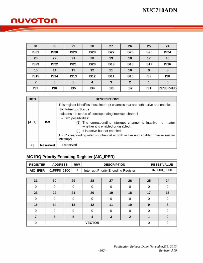
NUC710ADN
Publication Release Date: November235, 2013 - 362 - Revision A10
31 30 29 28 27 26 25 24
IS31 IS30 IS29 IS28 IS27 IS26 IS25 IS24
23 22 21 20 19 18 17 16
IS23 IS22 IS21 IS20 IS19 IS18 IS17 IS16
15 14 13 12 11 10 9 8
IS15 IS14 IS13 IS12 IS11 IS10 IS9 IS8
7 6 5 4 3 2 1 0
IS7 IS6 IS5 IS4 IS3 IS2 IS1 RESERVED
BITS DESCRIPTIONS
[31:1] ISx
This register identifies those interrupt channels that are both active and enabled. ISx: Interrupt Status Indicates the status of corresponding interrupt channel 0 = Two possibilities:
(1) The corresponding interrupt channel is inactive no matter whether it is enabled or disabled;
(2) It is active but not enabled 1 = Corresponding interrupt channel is both active and enabled (can assert an interrupt)
[0] Reserved Reserved
AIC IRQ Priority Encoding Register (AIC_IPER)
REGISTER ADDRESS R/W DESCRIPTION RESET VALUE
AIC_IPER 0xFFF8_210C R Interrupt Priority Encoding Register 0x0000_0000
31 30 29 28 27 26 25 24
0 0 0 0 0 0 0 0
23 22 21 20 19 18 17 16
0 0 0 0 0 0 0 0
15 14 13 12 11 10 9 8
0 0 0 0 0 0 0 0
7 6 5 4 3 2 1 0
0 VECTOR 0 0
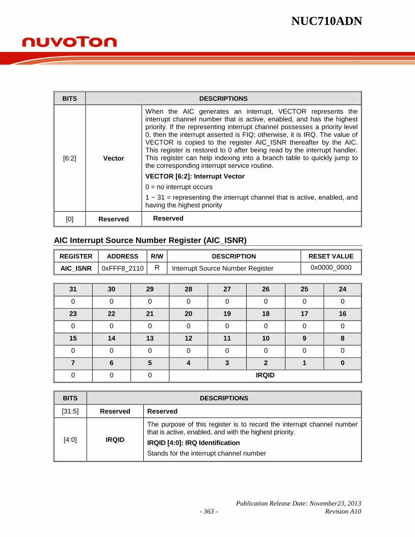
NUC710ADN
Publication Release Date: November23, 2013 - 363 - Revision A10
BITS DESCRIPTIONS
[6:2] Vector
When the AIC generates an interrupt, VECTOR represents the interrupt channel number that is active, enabled, and has the highest priority. If the representing interrupt channel possesses a priority level 0, then the interrupt asserted is FIQ; otherwise, it is IRQ. The value of VECTOR is copied to the register AIC_ISNR thereafter by the AIC. This register is restored to 0 after being read by the interrupt handler. This register can help indexing into a branch table to quickly jump to the corresponding interrupt service routine. VECTOR [6:2]: Interrupt Vector 0 = no interrupt occurs 1 ~ 31 = representing the interrupt channel that is active, enabled, and having the highest priority
[0] Reserved Reserved
AIC Interrupt Source Number Register (AIC_ISNR)
REGISTER ADDRESS R/W DESCRIPTION RESET VALUE
AIC_ISNR 0xFFF8_2110 R Interrupt Source Number Register 0x0000_0000
31 30 29 28 27 26 25 24
0 0 0 0 0 0 0 0
23 22 21 20 19 18 17 16
0 0 0 0 0 0 0 0
15 14 13 12 11 10 9 8
0 0 0 0 0 0 0 0
7 6 5 4 3 2 1 0
0 0 0 IRQID
BITS DESCRIPTIONS
[31:5] Reserved Reserved
[4:0] IRQID
The purpose of this register is to record the interrupt channel number that is active, enabled, and with the highest priority. IRQID [4:0]: IRQ Identification Stands for the interrupt channel number

NUC710ADN
Publication Release Date: November235, 2013 - 364 - Revision A10
AIC Interrupt Mask Register (AIC_IMR)
REGISTER ADDRESS R/W DESCRIPTION RESET VALUE
AIC_IMR 0xFFF8_2114 R Interrupt Mask Register 0x0000_0000
31 30 29 28 27 26 25 24 IM31 IM30 IM29 IM28 IM27 IM26 IM25 IM24
23 22 21 20 19 18 17 16 IM23 IM22 IM21 IM20 IM19 IM18 IM17 IM16
15 14 13 12 11 10 9 8 IM15 IM14 IM13 IM12 IM11 IM10 IM9 IM8
7 6 5 4 3 2 1 0 IM7 IM6 IM5 IM4 IM3 IM2 IM1 RESERVED
BITS DESCRIPTIONS
[31:1] IM x
IM x: Interrupt Mask This bit determines whether the corresponding interrupt channel is enabled or disabled. Every interrupt channel can be active no matter whether it is enabled or disabled. If an interrupt channel is enabled, it does not definitely mean it is active. Every interrupt channel can be authorized by the AIC only when it is both active and enabled. 0 = Corresponding interrupt channel is disabled 1 = Corresponding interrupt channel is enabled
[0] Reserved Reserved
AIC Output Interrupt Status Register (AIC_OISR)
REGISTER ADDRESS R/W DESCRIPTION RESET VALUE
AIC_OISR 0xFFF8_2118 R Output Interrupt Status Register 0x0000_0000
31 30 29 28 27 26 25 24 RESERVED
23 22 21 20 19 18 17 16 RESERVED
15 14 13 12 11 10 9 8 RESERVED
7 6 5 4 3 2 1 0 RESERVED IRQ FIQ
The AIC classifies the interrupt into FIQ and IRQ. This register indicates whether the asserted interrupt is FIQ or IRQ. If both IRQ and FIQ are equal to 0, it means that no interrupt occurred.
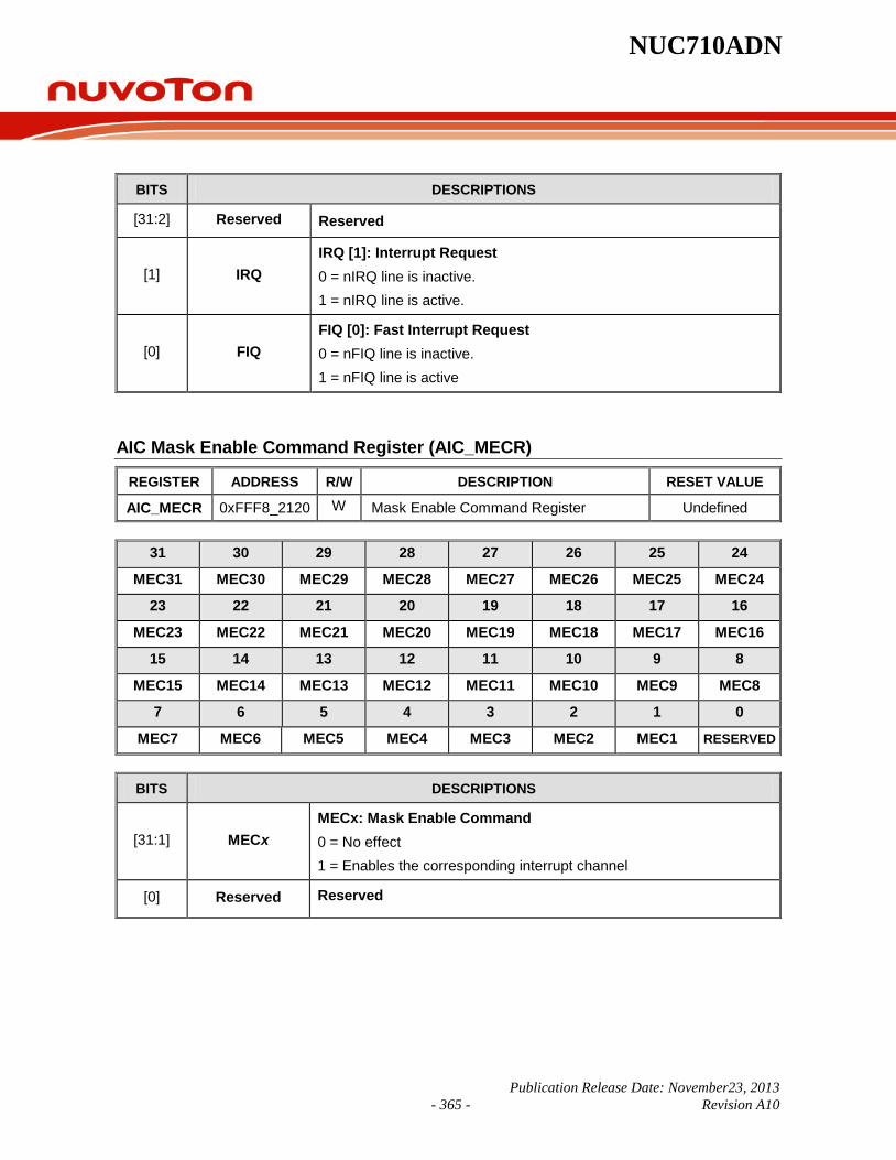
NUC710ADN
Publication Release Date: November23, 2013 - 365 - Revision A10
BITS DESCRIPTIONS
[31:2] Reserved Reserved
[1] IRQ IRQ [1]: Interrupt Request 0 = nIRQ line is inactive. 1 = nIRQ line is active.
[0] FIQ FIQ [0]: Fast Interrupt Request 0 = nFIQ line is inactive. 1 = nFIQ line is active
AIC Mask Enable Command Register (AIC_MECR)
REGISTER ADDRESS R/W DESCRIPTION RESET VALUE
AIC_MECR 0xFFF8_2120 W Mask Enable Command Register Undefined
31 30 29 28 27 26 25 24
MEC31 MEC30 MEC29 MEC28 MEC27 MEC26 MEC25 MEC24
23 22 21 20 19 18 17 16
MEC23 MEC22 MEC21 MEC20 MEC19 MEC18 MEC17 MEC16
15 14 13 12 11 10 9 8
MEC15 MEC14 MEC13 MEC12 MEC11 MEC10 MEC9 MEC8
7 6 5 4 3 2 1 0
MEC7 MEC6 MEC5 MEC4 MEC3 MEC2 MEC1 RESERVED
BITS DESCRIPTIONS
[31:1] MEC x MECx: Mask Enable Command 0 = No effect 1 = Enables the corresponding interrupt channel
[0] Reserved Reserved
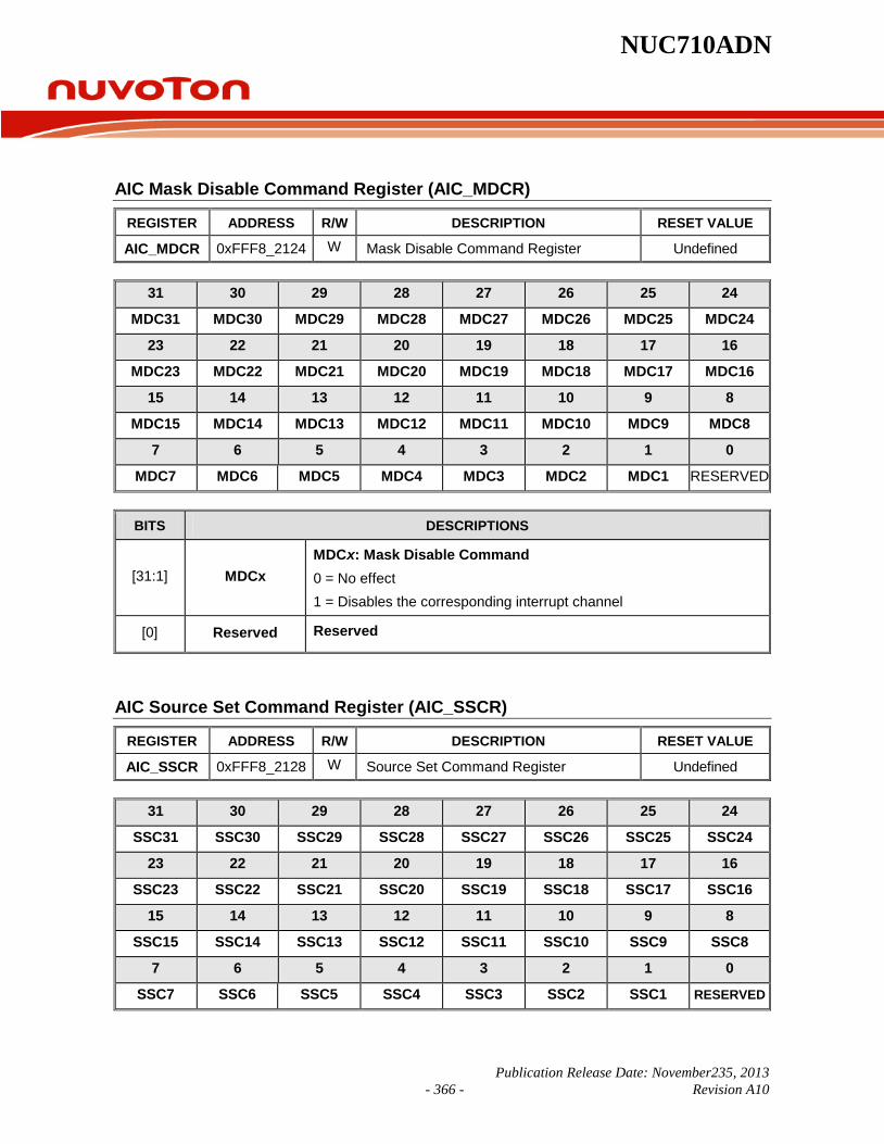
NUC710ADN
Publication Release Date: November235, 2013 - 366 - Revision A10
AIC Mask Disable Command Register (AIC_MDCR)
REGISTER ADDRESS R/W DESCRIPTION RESET VALUE
AIC_MDCR 0xFFF8_2124 W Mask Disable Command Register Undefined
31 30 29 28 27 26 25 24
MDC31 MDC30 MDC29 MDC28 MDC27 MDC26 MDC25 MDC24
23 22 21 20 19 18 17 16
MDC23 MDC22 MDC21 MDC20 MDC19 MDC18 MDC17 MDC16
15 14 13 12 11 10 9 8
MDC15 MDC14 MDC13 MDC12 MDC11 MDC10 MDC9 MDC8
7 6 5 4 3 2 1 0
MDC7 MDC6 MDC5 MDC4 MDC3 MDC2 MDC1 RESERVED
BITS DESCRIPTIONS
[31:1] MDCx MDC x: Mask Disable Command 0 = No effect 1 = Disables the corresponding interrupt channel
[0] Reserved Reserved
AIC Source Set Command Register (AIC_SSCR)
REGISTER ADDRESS R/W DESCRIPTION RESET VALUE
AIC_SSCR 0xFFF8_2128 W Source Set Command Register Undefined
31 30 29 28 27 26 25 24
SSC31 SSC30 SSC29 SSC28 SSC27 SSC26 SSC25 SSC24
23 22 21 20 19 18 17 16
SSC23 SSC22 SSC21 SSC20 SSC19 SSC18 SSC17 SSC16
15 14 13 12 11 10 9 8
SSC15 SSC14 SSC13 SSC12 SSC11 SSC10 SSC9 SSC8
7 6 5 4 3 2 1 0
SSC7 SSC6 SSC5 SSC4 SSC3 SSC2 SSC1 RESERVED
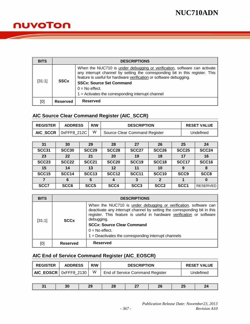
NUC710ADN
Publication Release Date: November23, 2013 - 367 - Revision A10
BITS DESCRIPTIONS
[31:1] SSCx
When the NUC710 is under debugging or verification, software can activate any interrupt channel by setting the corresponding bit in this register. This feature is useful for hardware verification or software debugging. SSCx: Source Set Command 0 = No effect. 1 = Activates the corresponding interrupt channel
[0] Reserved Reserved
AIC Source Clear Command Register (AIC_SCCR)
REGISTER ADDRESS R/W DESCRIPTION RESET VALUE
AIC_SCCR 0xFFF8_212C W Source Clear Command Register Undefined
31 30 29 28 27 26 25 24 SCC31 SCC30 SCC29 SCC28 SCC27 SCC26 SCC25 SCC24
23 22 21 20 19 18 17 16 SCC23 SCC22 SCC21 SCC20 SCC19 SCC18 SCC17 SCC16
15 14 13 12 11 10 9 8 SCC15 SCC14 SCC13 SCC12 SCC11 SCC10 SCC9 SCC8
7 6 5 4 3 2 1 0 SCC7 SCC6 SCC5 SCC4 SCC3 SCC2 SCC1 RESERVED
BITS DESCRIPTIONS
[31:1] SCCx
When the NUC710 is under debugging or verification, software can deactivate any interrupt channel by setting the corresponding bit in this register. This feature is useful in hardware verification or software debugging. SCCx: Source Clear Command 0 = No effect. 1 = Deactivates the corresponding interrupt channels
[0] Reserved Reserved
AIC End of Service Command Register (AIC_EOSCR)
REGISTER ADDRESS R/W DESCRIPTION RESET VALUE
AIC_EOSCR 0xFFF8_2130 W End of Service Command Register Undefined
31 30 29 28 27 26 25 24
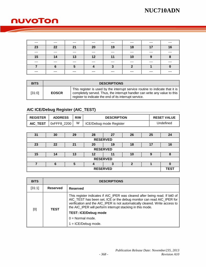
NUC710ADN
Publication Release Date: November235, 2013 - 368 - Revision A10
--- --- --- --- --- --- --- --- 23 22 21 20 19 18 17 16 --- --- --- --- --- --- --- --- 15 14 13 12 11 10 9 8 --- --- --- --- --- --- --- --- 7 6 5 4 3 2 1 0 --- --- --- --- --- --- --- ---
BITS DESCRIPTIONS
[31:0] EOSCR This register is used by the interrupt service routine to indicate that it is completely served. Thus, the interrupt handler can write any value to this register to indicate the end of its interrupt service.
AIC ICE/Debug Register (AIC_TEST)
REGISTER ADDRESS R/W DESCRIPTION RESET VALUE
AIC_TEST 0xFFF8_2200 W ICE/Debug mode Register Undefined
31 30 29 28 27 26 25 24
RESERVED 23 22 21 20 19 18 17 16
RESERVED 15 14 13 12 11 10 9 8
RESERVED 7 6 5 4 3 2 1 0
RESERVED TEST
BITS DESCRIPTIONS
[31:1] Reserved Reserved
[0] TEST
This register indicates if AIC_IPER was cleared after being read. If bit0 of AIC_TEST has been set, ICE or the debug monitor can read AIC_IPER for verification and the AIC_IPER is not automatically cleared. Write access to the AIC_IPER will perform interrupt stacking in this mode. TEST: ICE/Debug mode 0 = Normal mode. 1 = ICE/Debug mode.
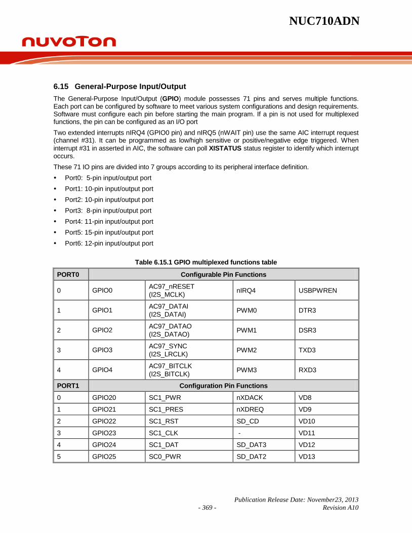
NUC710ADN
Publication Release Date: November23, 2013 - 369 - Revision A10
6.15 General-Purpose Input/Output The General-Purpose Input/Output (GPIO) module possesses 71 pins and serves multiple functions. Each port can be configured by software to meet various system configurations and design requirements. Software must configure each pin before starting the main program. If a pin is not used for multiplexed functions, the pin can be configured as an I/O port Two extended interrupts nIRQ4 (GPIO0 pin) and nIRQ5 (nWAIT pin) use the same AIC interrupt request (channel #31). It can be programmed as low/high sensitive or positive/negative edge triggered. When interrupt #31 in asserted in AIC, the software can poll XISTATUS status register to identify which interrupt occurs. These 71 IO pins are divided into 7 groups according to its peripheral interface definition. Port0: 5-pin input/output port Port1: 10-pin input/output port Port2: 10-pin input/output port Port3: 8-pin input/output port Port4: 11-pin input/output port Port5: 15-pin input/output port Port6: 12-pin input/output port
Table 6.15.1 GPIO multiplexed functions table
PORT0 Configurable Pin Functions
0 GPIO0 AC97_nRESET (I2S_MCLK) nIRQ4 USBPWREN
1 GPIO1 AC97_DATAI (I2S_DATAI) PWM0 DTR3
2 GPIO2 AC97_DATAO (I2S_DATAO) PWM1 DSR3
3 GPIO3 AC97_SYNC (I2S_LRCLK) PWM2 TXD3
4 GPIO4 AC97_BITCLK (I2S_BITCLK) PWM3 RXD3
PORT1 Configuration Pin Functions
0 GPIO20 SC1_PWR nXDACK VD8
1 GPIO21 SC1_PRES nXDREQ VD9
2 GPIO22 SC1_RST SD_CD VD10
3 GPIO23 SC1_CLK - VD11
4 GPIO24 SC1_DAT SD_DAT3 VD12
5 GPIO25 SC0_PWR SD_DAT2 VD13

NUC710ADN
Publication Release Date: November235, 2013 - 370 - Revision A10
Table 6.15.1 GPIO multiplexed functions table, continued
6 GPIO26 SC0_PRES SD_DAT1 VD14
7 GPIO27 SC0_RST SD_DAT0 VD15
8 GPIO28 SC0_CLK SD_CLK VD16
9 GPIO29 SC0_DAT SD_CMD VD17
PORT2 Configuration Pin Functions
0 GPIO42 PHY_RXERR KPCOL0 VD8
1 GPIO43 PHY_CRSDV KPCOL1 VD9
2 GPIO44 PHY_RXD[0] KPCOL2 VD10
3 GPIO45 PHY_RXD[1] KPCOL3 VD11
4 GPIO46 PHY_REFCLK KPCOL4 VD12
5 GPIO47 PHY_TXEN KPCOL5 VD13
6 GPIO48 PHY_TXD[0] KPCOL6 VD14
7 GPIO49 PHY_TXD[1] KPCOL7 VD15
8 GPIO50 PHY_MDIO KPROW0 VD16
9 GPIO51 PHY_MDC KPROW1 VD17
PORT3 Configuration Pin Functions
0 GPIO60 D24 VD16 -
1 GPIO61 D25 VD17 -
2 GPIO62 D26 VD18 -
3 GPIO63 D27 VD19 -
4 GPIO64 D28 VD20 -
5 GPIO65 D29 VD21 -
6 GPIO66 D30 VD22 -
7 GPIO67 D31 VD23 -
PORT4 Configuration Pin Functions
0 GPIO52 D16 VD8 -
1 GPIO53 D17 VD9 -
2 GPIO54 D18 VD10 -
3 GPIO55 D19 VD11 -
4 GPIO56 D20 VD12 -
5 GPIO57 D21 VD13 -
6 GPIO58 D22 VD14 -

NUC710ADN
Publication Release Date: November23, 2013 - 371 - Revision A10
Table 6.15.1 GPIO multiplexed functions table, continued
7 GPIO59 D23 VD15 - 8 GPIO68 nWBE2/SDQM2 - - 9 GPIO69 nWBE3/SDQM3 - - 10 GPIO70 nWAIT nIRQ5 - PORT5 Configuration Pin Functions 0 GPIO5 TXD0 - - 1 GPIO6 RXD0 - - 2 GPIO7 TXD1 - - 3 GPIO8 RXD1 - - 4 GPIO9 TXD2 CTS1 PS2CLK 5 GPIO10 RXD2 RTS1 PS2DATA 6 GPIO11 SCL0 SFRM TIMER0 7 GPIO12 SDA0 SSPTXD TIMER1 8 GPIO13 SCL1 SCLK KPROW3 9 GPIO14 SDA1 SSPRXD KPROW2 10 GPIO15 nWDOG USBPWREN - 11 GPIO16 nIRQ0 - - 12 GP1O17 nIRQ1 USBOVRCUR - 13 GPIO18 nIRQ2 - 14 GPIO19 nIRQ3 - - PORT6 Configuration Pin Function 0 GPIO30 VCLK KPROW0 - 1 GPIO31 VDEN KPROW1 2 GPIO32 VSYNC KPROW2 - 3 GPIO33 HSYNC KPROW3 - 4 GPIO34 VD0 KPCOL0 - 5 GPIO35 VD1 KPCOL1 - 6 GPIO36 VD2 KPCOL2 - 7 GPIO37 VD3 KPCOL3 - 8 GPIO38 VD4 KPCOL4 - 9 GPIO39 VD5 KPCOL5 - 10 GPIO40 VD6 KPCOL6 - 11 GPIO41 VD7 KPCOL7 -

NUC710ADN
Publication Release Date: November235, 2013 - 372 - Revision A10
6.15.1 GPIO Control Registers Map
REGISTER ADDRESS R/W DESCRIPTION RESET VALUE
GPIO_CFG0 0xFFF8_3000 R/W GPIO port0 configuration register 0x0000_0000
GPIO_DIR0 0xFFF8_3004 R/W GPIO port0 direction control register 0x0000_0000
GPIO_DATAOUT0 0xFFF8_3008 R/W GPIO port0 data output register 0x0000_0000
GPIO_DATAIN0 0xFFF8_300C R GPIO port0 data input register 0xXXXX_XXXX
GPIO_CFG1 0xFFF8_3010 R/W GPIO port1 configuration register 0x0000_0000
GPIO_DIR1 0xFFF8_3014 R/W GPIO port1 direction control register 0x0000_0000
GPIO_DATAOUT1 0xFFF8_3018 R/W GPIO port1 data output register 0x0000_0000
GPIO_DATAIN1 0xFFF8_301C R GPIO port1 data input register 0xXXXX_XXXX
GPIO_CFG2 0xFFF8_3020 R/W GPIO port2 configuration register 0x0000_0000
GPIO_DIR2 0xFFF8_3024 R/W GPIO port2 direction control register 0x0000_0000
GPIO_DATAOUT2 0xFFF8_3028 R/W GPIO port2 data output register 0x0000_0000
GPIO_DATAIN2 0xFFF8_302C R GPIO port2 data input register 0x0000_0000
GPIO_CFG3 0xFFF8_3030 R/W GPIO port3 configuration register 0x0000_5555
GPIO_DIR3 0xFFF8_3034 R/W GPIO port3 direction control register 0x0000_0000
GPIO_DATAOUT3 0xFFF8_3038 R/W GPIO port3 data output register 0x0000_0000
GPIO_DATAIN3 0xFFF8_303C R GPIO port3 data input register 0xXXXX_XXXX
GPIO_CFG4 0xFFF8_3040 R/W GPIO port4 configuration register 0x0015_5555
GPIO_DIR4 0xFFF8_3044 R/W GPIO port4 direction control register 0x0000_0000
GPIO_DATAOUT4 0xFFF8_3048 R/W GPIO port4 data output register 0x0000_0000
GPIO_DATAIN4 0xFFF8_304C R GPIO port4 data input register 0xXXXX_XXXX

NUC710ADN
Publication Release Date: November23, 2013 - 373 - Revision A10
GPIO Control Registers Map, continued
REGISTER ADDRESS R/W DESCRIPTION RESET VALUE
GPIO_CFG5 0xFFF8_3050 R/W GPIO port5 configuration register 0x0000_0000
GPIO_DIR5 0xFFF8_3054 R/W GPIO port5 direction control register 0x0000_0000
GPIO_DATAOUT5 0xFFF8_3058 R/W GPIO port5 data output register 0x0000_0000
GPIO_DATAIN5 0xFFF8_305C R GPIO port5 data input register 0xXXXX_XXXX
GPIO_CFG6 0xFFF8_3060 R/W GPIO port6 configuration register 0x0000_0000
GPIO_DIR6 0xFFF8_3064 R/W GPIO port6 direction control register 0x0000_0000
GPIO_DATAOUT6 0xFFF8_3068 R/W GPIO port6 data output register 0x0000_0000
GPIO_DATAIN6 0xFFF8_306C R GPIO port6 data input register 0xXXXX_XXXX
GPIO_DBNCECON 0xFFF8_3070 R/W GPIO input debounce control register 0x0000_0000
GPIO_XICFG 0xFFF8_3074 R/W Extend Interrupt Configure Register 0xXXXX_XXX0
GPIO_XISTATUS 0xFFF8_3078 R/W Extend Interrupt Status Register 0xXXXX_XXX0
6.15.2 GPIO Register Description
GPIO Port0 Configuration Register (GPIO_CFG0)
REGISTER ADDRESS R/W DESCRIPTION RESET VALUE
GPIO_CFG0 0xFFF8_3000 R/W GPIO port0 configuration register 0x0000_0000
31 30 29 28 27 26 25 24
RESERVED
23 22 21 20 19 18 17 16
RESERVED
15 14 13 12 11 10 9 8
RESERVED PT0CFG4
7 6 5 4 3 2 1 0
PT0CFG3 PT0CFG2 PT0CFG1 PT0CFG0
PT0CFG0 11 10 01 00
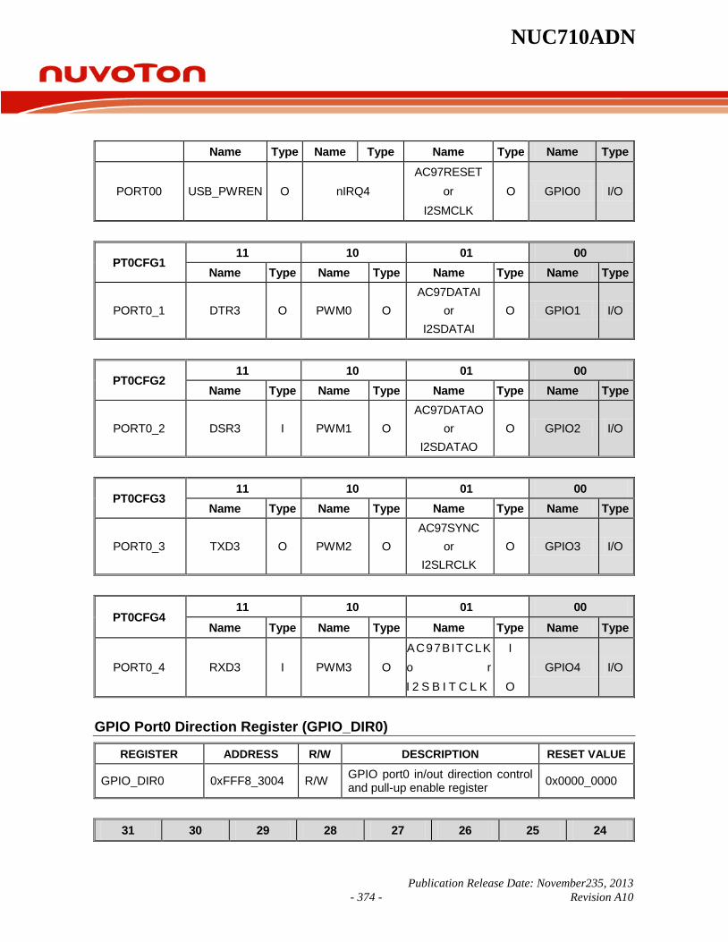
NUC710ADN
Publication Release Date: November235, 2013 - 374 - Revision A10
Name Type Name Type Name Type Name Type
PORT00 USB_PWREN O nIRQ4 AC97RESET
or I2SMCLK
O GPIO0 I/O
PT0CFG1 11 10 01 00
Name Type Name Type Name Type Name Type
PORT0_1 DTR3 O PWM0 O AC97DATAI
or I2SDATAI
O GPIO1 I/O
PT0CFG2 11 10 01 00
Name Type Name Type Name Type Name Type
PORT0_2 DSR3 I PWM1 O AC97DATAO
or I2SDATAO
O GPIO2 I/O
PT0CFG3 11 10 01 00
Name Type Name Type Name Type Name Type
PORT0_3 TXD3 O PWM2 O AC97SYNC
or I2SLRCLK
O GPIO3 I/O
PT0CFG4 11 10 01 00
Name Type Name Type Name Type Name Type
PORT0_4 RXD3 I PWM3 O AC97BITCLK o r I 2 S B I T C L K
I
O GPIO4 I/O
GPIO Port0 Direction Register (GPIO_DIR0)
REGISTER ADDRESS R/W DESCRIPTION RESET VALUE
GPIO_DIR0 0xFFF8_3004 R/W GPIO port0 in/out direction control and pull-up enable register 0x0000_0000
31 30 29 28 27 26 25 24

NUC710ADN
Publication Release Date: November23, 2013 - 375 - Revision A10
RESERVED
23 22 21 20 19 18 17 16
RESERVED PUPEN0[3:0]
15 14 13 12 11 10 9 8
RESERVED
7 6 5 4 3 2 1 0
RESERVED OMDEN0[4:0]
Bits Description [31:20] RESERVED -
[19:16] PUPEN0
GPIO3 -GPIO0 port pin internal pull-up resister enable There are 4 bits for this register, setting a bit to 1enables a pull-up resister on an I/O pin. 1 = Enable pull-up resister 0 = Disable pull-up resister After power on, the pull-up resisters are disabled. NOTE: GPIO4 is used as AC97 BITCLK input, an I/O pad with Schmitt trigger input buffer PDB04SDGZ is implemented for this pin. Due to TSMC I/O library without a pull-up register, an external pull-up resister is necessary.
[15:5] RESERVED
[4:0] OMDEN0
GPIO4 ~GPIO0 output mode enable 1 = Enable GPIOx output mode 0 = GPIOx is input mode NOTE: Output mode enable bits are valid only when bit PT0CFG4-0 is configured for general purpose I/O. Each port pin can be enabled individually by setting the corresponding control bit.
GPIO Port0 Data Output Register (GPIO_DATAOUT0)
REGISTER ADDRESS R/W DESCRIPTION RESET VALUE
GPIO_DATAOUT0 0xFFF8_3008 R/W GPIO port0 data output register 0x0000_0000
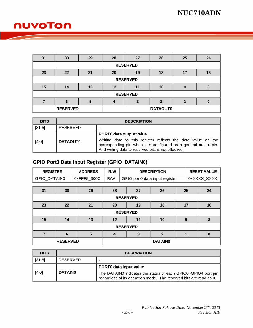
NUC710ADN
Publication Release Date: November235, 2013 - 376 - Revision A10
31 30 29 28 27 26 25 24
RESERVED
23 22 21 20 19 18 17 16
RESERVED
15 14 13 12 11 10 9 8
RESERVED
7 6 5 4 3 2 1 0
RESERVED DATAOUT0
BITS DESCRIPTION [31:5] RESERVED -
[4:0] DATAOUT0
PORT0 data output value Writing data to this register reflects the data value on the corresponding pin when it is configured as a general output pin. And writing data to reserved bits is not effective.
GPIO Port0 Data Input Register (GPIO_DATAIN0)
REGISTER ADDRESS R/W DESCRIPTION RESET VALUE
GPIO_DATAIN0 0xFFF8_300C R/W GPIO port0 data input register 0xXXXX_XXXX
31 30 29 28 27 26 25 24
RESERVED
23 22 21 20 19 18 17 16
RESERVED
15 14 13 12 11 10 9 8
RESERVED
7 6 5 4 3 2 1 0
RESERVED DATAIN0
BITS DESCRIPTION [31:5] RESERVED -
[4:0] DATAIN0 PORT0 data input value The DATAIN0 indicates the status of each GPIO0~GPIO4 port pin regardless of its operation mode. The reserved bits are read as 0.

NUC710ADN
Publication Release Date: November23, 2013 - 377 - Revision A10
GPIO Port1 Configuration Register (GPIO_CFG1)
REGISTER ADDRESS R/W DESCRIPTION RESET VALUE
GPIO_CFG1 0xFFF8_3010 R/W GPIO port1 configuration register 0x0000_0000
31 30 29 28 27 26 25 24 RESERVED
23 22 21 20 19 18 17 16 RESERVED PT1CFG9 PT1CFG8
15 14 13 12 11 10 9 8 PT1CFG7 PT1CFG6 PT1CFG5 PT1CFG4
7 6 5 4 3 2 1 0 PT1CFG3 PT1CFG2 PT1CFG1 PT1CFG0
*In the following pin definition, the shaded functions are default.
PT1CFG0 11 10 01 00
Name Type Name Type Name Type Name Type PORT1_0 VD8 SC1_PWR O nXDACK O GPIO20 I/O
PT1CFG1 11 10 01 00
Name Type Name Type Name Type Name Type PORT1_1 VD9 SC1_PRES I nXDREQ I GPIO21 I/O
PT1CFG2 11 10 01 00
Name Type Name Type Name Type Name Type PORT1_2 VD10 SC1_RST O SD_CD I GPIO22 I/O
PT1CFG3 11 10 01 00
Name Type Name Type Name Type Name Type PORT1_3 VD11 SC1_CLK O RESERVED GPIO23 I/O
PT1CFG4 11 10 01 00
Name Type Name Type Name Type Name Type PORT1_4 VD12 SC1_DAT O SD_DAT3 I/O GPIO24 I/O
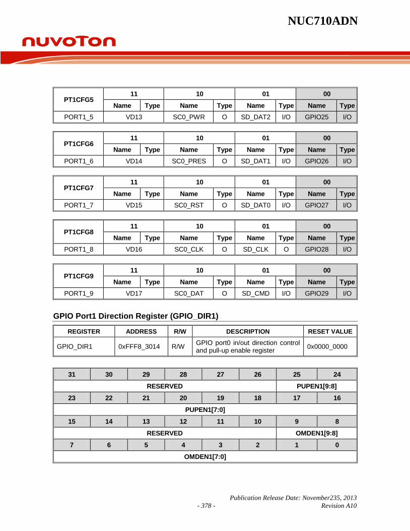
NUC710ADN
Publication Release Date: November235, 2013 - 378 - Revision A10
PT1CFG5 11 10 01 00
Name Type Name Type Name Type Name Type PORT1_5 VD13 SC0_PWR O SD_DAT2 I/O GPIO25 I/O
PT1CFG6 11 10 01 00
Name Type Name Type Name Type Name Type PORT1_6 VD14 SC0_PRES O SD_DAT1 I/O GPIO26 I/O
PT1CFG7 11 10 01 00
Name Type Name Type Name Type Name Type PORT1_7 VD15 SC0_RST O SD_DAT0 I/O GPIO27 I/O
PT1CFG8 11 10 01 00
Name Type Name Type Name Type Name Type PORT1_8 VD16 SC0_CLK O SD_CLK O GPIO28 I/O
PT1CFG9 11 10 01 00
Name Type Name Type Name Type Name Type PORT1_9 VD17 SC0_DAT O SD_CMD I/O GPIO29 I/O
GPIO Port1 Direction Register (GPIO_DIR1)
REGISTER ADDRESS R/W DESCRIPTION RESET VALUE
GPIO_DIR1 0xFFF8_3014 R/W GPIO port0 in/out direction control and pull-up enable register 0x0000_0000
31 30 29 28 27 26 25 24
RESERVED PUPEN1[9:8]
23 22 21 20 19 18 17 16
PUPEN1[7:0]
15 14 13 12 11 10 9 8
RESERVED OMDEN1[9:8]
7 6 5 4 3 2 1 0
OMDEN1[7:0]

NUC710ADN
Publication Release Date: November23, 2013 - 379 - Revision A10
BITS DESCRIPTION [31:26] RESERVED -
[25:16] PUPEN1
GPIO51 ~ GPIO42 port pins internal pull-up resistor enable This is a 10-bit register. Setting a bit to 1 enables the corresponding pull up resistor I/O pin. 1 = Enable pull-up resister 0 = Disable pull-up resister After power on, the resistors are disabled.
[15:10] RESERVED -
[9:0] OMDEN1
GPIO51 ~ GPIO42 output mode enable 1 = Enable GPIOx output mode 0 = GPIOx is input mode NOTE: Output mode enable bits are valid only when bit PT1CFG9-0 is configured as general purpose I/O mode.Each port pin can be enabled individually by setting the corresponding control bit.
GPIO Port1 Data Output Register (GPIO_DATAOUT1)
REGISTER ADDRESS R/W DESCRIPTION RESET VALUE
GPIO_DATAOUT1 0xFFF8_3018 R/W GPIO port1 data output register 0x0000_0000
31 30 29 28 27 26 25 24
RESERVED
23 22 21 20 19 18 17 16
RESERVED
15 14 13 12 11 10 9 8
RESERVED DATAOUT1[9:8]
7 6 5 4 3 2 1 0
DATAOUT1[7:0]
BITS DESCRIPTION
[31:10] RESERVED -
[9:0] DATAOUT1
PORT1 data output value Writing data to this register reflects the data value on the corresponding port1 pin when it is configured as a general-purpose output pin. And writing data to reserved bits is not effective.

NUC710ADN
Publication Release Date: November235, 2013 - 380 - Revision A10
GPIO Port1 Data Input Register (GPIO_DATAIN1)
REGISTER ADDRESS R/W DESCRIPTION RESET VALUE
GPIO_DATAIN1 0xFFF8_301C R/W GPIO port1 data input register 0xXXXX_XXXX
31 30 29 28 27 26 25 24
RESERVED
23 22 21 20 19 18 17 16
RESERVED
15 14 13 12 11 10 9 8
RESERVED DATAIN1[9:8]
7 6 5 4 3 2 1 0
DATAIN1[7:0]
BITS DESCRIPTION
[31:10] RESERVED -
[9:0] DATAIN1 Port1 input data register DATAIN1 indicates the status of each GPIO29~GPIO20 pin regardless of its operating mode. The reserved bits are read as 0s.
GPIO Port2 Configuration Register (GPIO_CFG2)
REGISTER ADDRESS R/W DESCRIPTION RESET VALUE
GPIO_CFG2 0xFFF8_3020 R/W GPIO port2 configuration register 0x0000_0000
31 30 29 28 27 26 25 24
RESERVED
23 22 21 20 19 18 17 16
RESERVED PT2CFG9 PT2CFG8
15 14 13 12 11 10 9 8
PT2CFG7 PT2CFG6 PT2CFG5 PT2CFG4
7 6 5 4 3 2 1 0
PT2CFG3 PT2CFG2 PT2CFG1 PT2CFG0

NUC710ADN
Publication Release Date: November23, 2013 - 381 - Revision A10
*In the following pin definition, shaded functions are set by default.
PT2CFG0 11 10 01 00
Name Type Name Type Name Type Name Type PORT2_0 VD8 O KPCOL0 I PHY_RXERR I GPIO42 I/O
PT2CFG1 11 10 01 00
Name Type Name Type Name Type Name Type PORT2_1 VD9 O KPCOL1 I PHY_CRSDV I GPIO43 I/O
PT2CFG2 11 10 01 00
Name Type Name Type Name Type Name Type PORT2_2 VD10 O KPCOL2 I PHY_RXD[0] I GPIO44 I/O
PT2CFG3 11 10 01 00
Name Type Name Type Name Type Name Type PORT2_3 VD11 O KPCOL3 I PHY_RXD[1] I GPIO45 I/O
PT2CFG4 11 10 01 00
Name Type Name Type Name Type Name Type PORT2_4 VD12 O KPCOL4 I PHY_REFCLK I GPIO46 I/O
PT2CFG5 11 10 01 00
Name Type Name Type Name Type Name Type PORT2_5 VD13 O KPCOL5 I PHY_TXEN O GPIO47 I/O
PT2CFG6 11 10 01 00
Name Type Name Type Name Type Name Type PORT2_6 VD14 O KPCOL6 I PHY_TXD[0] O GPIO48 I/O
PT2CFG7 11 10 01 00
Name Type Name Type Name Type Name Type PORT2_7 VD15 O KPCOL7 I PHY_TXD[1] O GPIO49 I/O
PT2CFG8 11 10 01 00
Name Type Name Type Name Type Name Type PORT2_8 VD16 O KPROW0 O PHY_MDIO I/O GPIO50 I/O

NUC710ADN
Publication Release Date: November235, 2013 - 382 - Revision A10
PT2CFG9 11 10 01 00
Name Type Name Type Name Type Name Type PORT2_9 VD17 O KPROW1 O PHY_MDC O GPIO51 I/O
GPIO Port2 Direction Register (GPIO_DIR2)
REGISTER ADDRESS R/W DESCRIPTION RESET VALUE
GPIO_DIR2 0xFFF8_3024 R/W GPIO port2 in/out direction control and pull-up enable register 0x0000_0000
31 30 29 28 27 26 25 24
RESERVED PUPEN2[9:8]
23 22 21 20 19 18 17 16
PUPEN2[7:0]
15 14 13 12 11 10 9 8
RESERVED OMDEN2[9:8]
7 6 5 4 3 2 1 0
OMDEN2[7:0]
BITS DESCRIPTION [31:26] RESERVED -
[25:16] PUPEN2
GPIO51 ~ GPIO42 port pin internal pull-up resistor enable This is a 10-bit register; setting a bit to 1 enables the corresponding pull-up resistor I/O pin. 1 = Enable pull-up resister 0 = Disable pull-up resister After power on, the registers are disabled.
[15:10] RESERVED
[9:0] OMDEN2
GPIO51 ~ GPIO42 output mode enable 1 = Enable GPIOx output mode 0 = GPIOx is input mode NOTE: Output mode enable bits are valid only when bit PT2CFG7-0 is configured as a general purpose I/O mode. Each port pin can be enabled individually by setting the corresponding control bit.

NUC710ADN
Publication Release Date: November23, 2013 - 383 - Revision A10
PGPIO Port2 Data Output Register (GPIO_DATAOUT2)
REGISTER ADDRESS R/W DESCRIPTION RESET VALUE
GPIO_DATAOUT2 0xFFF8_3028 R/W GPIO port2 data output register 0x0000_0000
31 30 29 28 27 26 25 24
RESERVED
23 22 21 20 19 18 17 16
RESERVED
15 14 13 12 11 10 9 8
RESERVED DATAOUT2[9:8]
7 6 5 4 3 2 1 0
DATAOUT2[7:0]
BITS DESCRIPTION
[31:10] RESERVED -
[9:0] DATAOUT2
PORT2 data output value Writing data to this register reflects the data value on the corresponding port2 pin when it is configured as a general-purpose output pin. And writing data to reserved bits is not effective.
GPIO Port2 Data Input Register (GPIO_DATAIN2)
REGISTER ADDRESS R/W DESCRIPTION RESET VALUE
GPIO_DATAIN2 0xFFF8_302C R/W GPIO port2 data input register 0xXXXX_XXXX
31 30 29 28 27 26 25 24
RESERVED
23 22 21 20 19 18 17 16
RESERVED
15 14 13 12 11 10 9 8
RESERVED DATAIN2[9:8]
7 6 5 4 3 2 1 0
DATAIN2[7:0] BITS DESCRIPTION
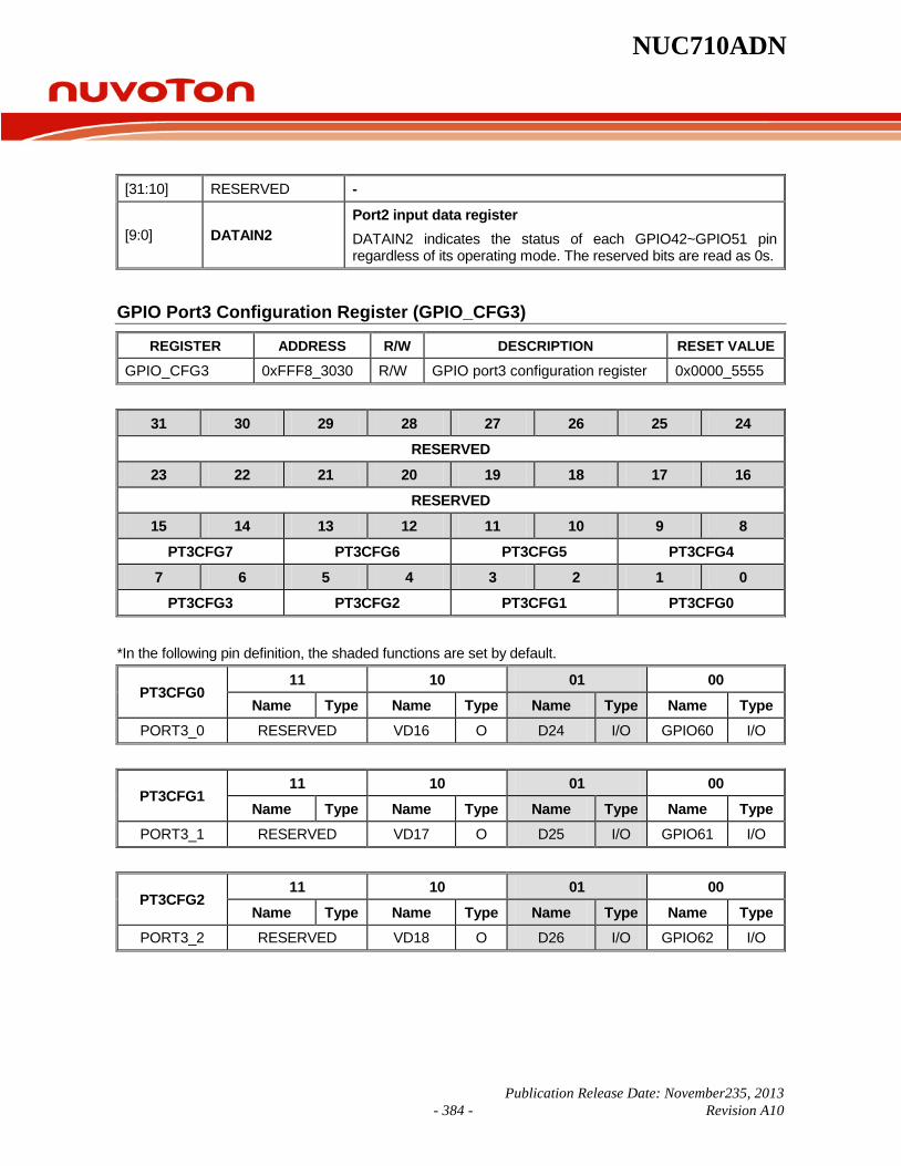
NUC710ADN
Publication Release Date: November235, 2013 - 384 - Revision A10
[31:10] RESERVED -
[9:0] DATAIN2 Port2 input data register DATAIN2 indicates the status of each GPIO42~GPIO51 pin regardless of its operating mode. The reserved bits are read as 0s.
GPIO Port3 Configuration Register (GPIO_CFG3)
REGISTER ADDRESS R/W DESCRIPTION RESET VALUE
GPIO_CFG3 0xFFF8_3030 R/W GPIO port3 configuration register 0x0000_5555
31 30 29 28 27 26 25 24
RESERVED
23 22 21 20 19 18 17 16
RESERVED
15 14 13 12 11 10 9 8
PT3CFG7 PT3CFG6 PT3CFG5 PT3CFG4
7 6 5 4 3 2 1 0
PT3CFG3 PT3CFG2 PT3CFG1 PT3CFG0
*In the following pin definition, the shaded functions are set by default.
PT3CFG0 11 10 01 00
Name Type Name Type Name Type Name Type PORT3_0 RESERVED VD16 O D24 I/O GPIO60 I/O
PT3CFG1 11 10 01 00
Name Type Name Type Name Type Name Type PORT3_1 RESERVED VD17 O D25 I/O GPIO61 I/O
PT3CFG2 11 10 01 00
Name Type Name Type Name Type Name Type PORT3_2 RESERVED VD18 O D26 I/O GPIO62 I/O
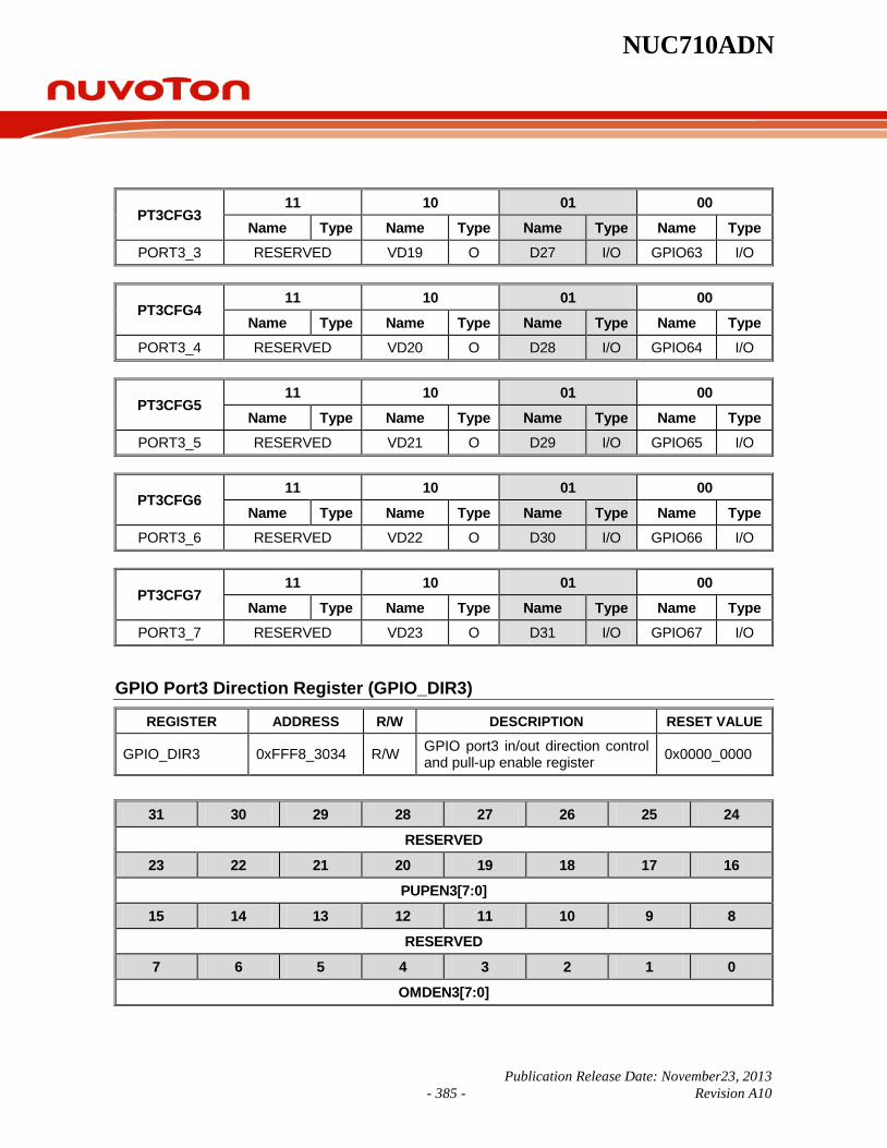
NUC710ADN
Publication Release Date: November23, 2013 - 385 - Revision A10
PT3CFG3 11 10 01 00
Name Type Name Type Name Type Name Type PORT3_3 RESERVED VD19 O D27 I/O GPIO63 I/O
PT3CFG4 11 10 01 00
Name Type Name Type Name Type Name Type PORT3_4 RESERVED VD20 O D28 I/O GPIO64 I/O
PT3CFG5 11 10 01 00
Name Type Name Type Name Type Name Type PORT3_5 RESERVED VD21 O D29 I/O GPIO65 I/O
PT3CFG6 11 10 01 00
Name Type Name Type Name Type Name Type PORT3_6 RESERVED VD22 O D30 I/O GPIO66 I/O
PT3CFG7 11 10 01 00
Name Type Name Type Name Type Name Type PORT3_7 RESERVED VD23 O D31 I/O GPIO67 I/O
GPIO Port3 Direction Register (GPIO_DIR3)
REGISTER ADDRESS R/W DESCRIPTION RESET VALUE
GPIO_DIR3 0xFFF8_3034 R/W GPIO port3 in/out direction control and pull-up enable register 0x0000_0000
31 30 29 28 27 26 25 24
RESERVED
23 22 21 20 19 18 17 16
PUPEN3[7:0]
15 14 13 12 11 10 9 8
RESERVED
7 6 5 4 3 2 1 0
OMDEN3[7:0]
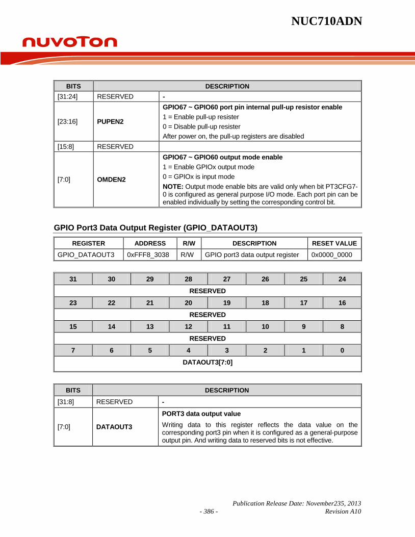
NUC710ADN
Publication Release Date: November235, 2013 - 386 - Revision A10
BITS DESCRIPTION [31:24] RESERVED -
[23:16] PUPEN2
GPIO67 ~ GPIO60 port pin internal pull-up resistor enable 1 = Enable pull-up resister 0 = Disable pull-up resister After power on, the pull-up registers are disabled
[15:8] RESERVED
[7:0] OMDEN2
GPIO67 ~ GPIO60 output mode enable 1 = Enable GPIOx output mode 0 = GPIOx is input mode NOTE: Output mode enable bits are valid only when bit PT3CFG7-0 is configured as general purpose I/O mode. Each port pin can be enabled individually by setting the corresponding control bit.
GPIO Port3 Data Output Register (GPIO_DATAOUT3)
REGISTER ADDRESS R/W DESCRIPTION RESET VALUE
GPIO_DATAOUT3 0xFFF8_3038 R/W GPIO port3 data output register 0x0000_0000
31 30 29 28 27 26 25 24
RESERVED
23 22 21 20 19 18 17 16
RESERVED
15 14 13 12 11 10 9 8
RESERVED
7 6 5 4 3 2 1 0
DATAOUT3[7:0]
BITS DESCRIPTION
[31:8] RESERVED -
[7:0] DATAOUT3
PORT3 data output value Writing data to this register reflects the data value on the corresponding port3 pin when it is configured as a general-purpose output pin. And writing data to reserved bits is not effective.

NUC710ADN
Publication Release Date: November23, 2013 - 387 - Revision A10
GPIO Port3 Data Input Register (GPIO_DATAIN3)
REGISTER ADDRESS R/W DESCRIPTION RESET VALUE
GPIO_DATAIN3 0xFFF8_303C R/W GPIO port3 data input register 0xXXXX_XXXX
31 30 29 28 27 26 25 24
RESERVED
23 22 21 20 19 18 17 16
RESERVED
15 14 13 12 11 10 9 8
RESERVED
7 6 5 4 3 2 1 0
DATAIN3[7:0]
BITS DESCRIPTION
[31:8] RESERVED -
[7:0] DATAIN3 Port3 input data register The DATAIN3 indicates the status of each GPIO67~GPIO60 pin regardless of its operation mode. The reserved bits is read as 0s.
GPIO Port4 Configuration Register (GPIO_CFG4)
REGISTER ADDRESS R/W DESCRIPTION RESET VALUE
GPIO_CFG4 0xFFF8_3040 R/W GPIO port4 configuration register 0x0015_5555
31 30 29 28 27 26 25 24
RESERVED
23 22 21 20 19 18 17 16
RESERVED PT4CFG10 PT4CFG9 PT4CFG8
15 14 13 12 11 10 9 8
PT4CFG7 PT4CFG6 PT4CFG5 PT4CFG4
7 6 5 4 3 2 1 0
PT4CFG3 PT4CFG2 PT4CFG1 PT4CFG0
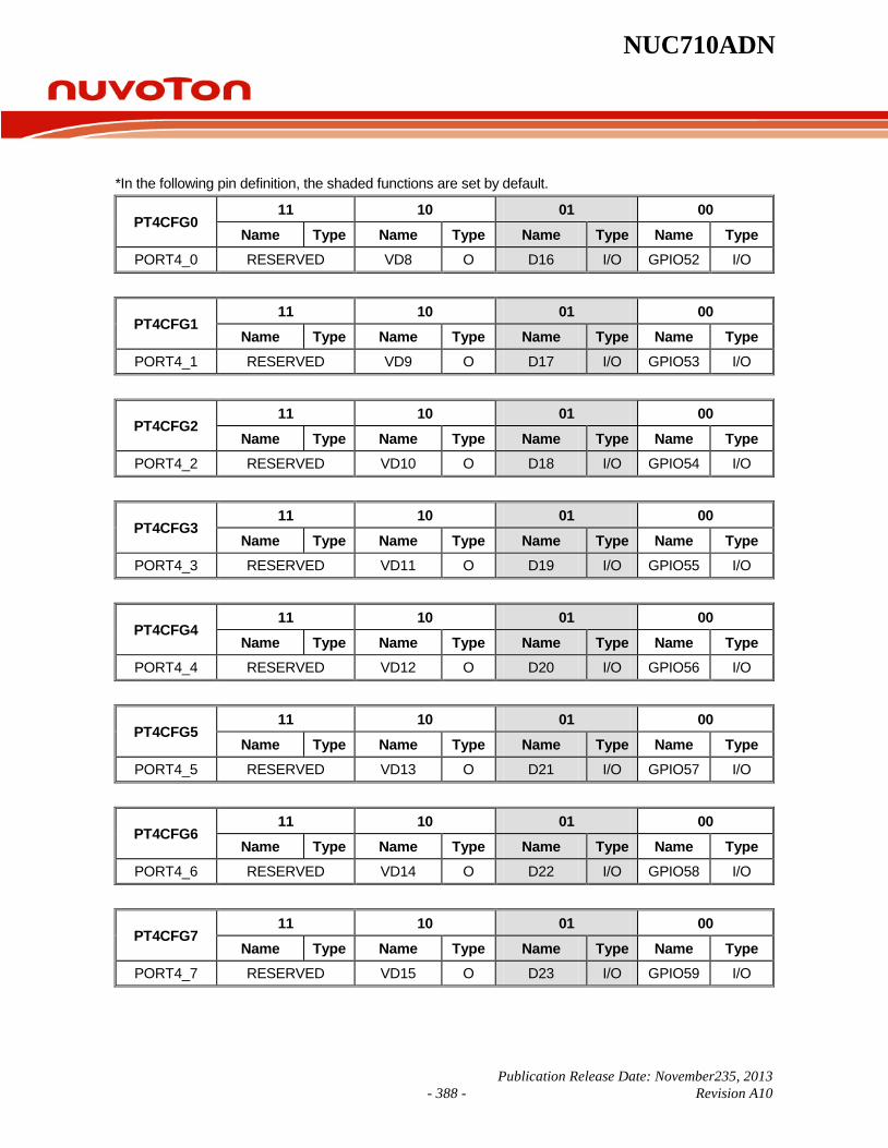
NUC710ADN
Publication Release Date: November235, 2013 - 388 - Revision A10
*In the following pin definition, the shaded functions are set by default.
PT4CFG0 11 10 01 00
Name Type Name Type Name Type Name Type PORT4_0 RESERVED VD8 O D16 I/O GPIO52 I/O
PT4CFG1 11 10 01 00
Name Type Name Type Name Type Name Type PORT4_1 RESERVED VD9 O D17 I/O GPIO53 I/O
PT4CFG2 11 10 01 00
Name Type Name Type Name Type Name Type PORT4_2 RESERVED VD10 O D18 I/O GPIO54 I/O
PT4CFG3 11 10 01 00
Name Type Name Type Name Type Name Type PORT4_3 RESERVED VD11 O D19 I/O GPIO55 I/O
PT4CFG4 11 10 01 00
Name Type Name Type Name Type Name Type PORT4_4 RESERVED VD12 O D20 I/O GPIO56 I/O
PT4CFG5 11 10 01 00
Name Type Name Type Name Type Name Type PORT4_5 RESERVED VD13 O D21 I/O GPIO57 I/O
PT4CFG6 11 10 01 00
Name Type Name Type Name Type Name Type PORT4_6 RESERVED VD14 O D22 I/O GPIO58 I/O
PT4CFG7 11 10 01 00
Name Type Name Type Name Type Name Type PORT4_7 RESERVED VD15 O D23 I/O GPIO59 I/O

NUC710ADN
Publication Release Date: November23, 2013 - 389 - Revision A10
PT4CFG8 11 10 01 00
Name Type Name Type Name Type Name Type PORT4_8 RESERVED RESERVED nWBE2/SDQM2 I/O GPIO68 I/O
PT4CFG9 11 10 01 00
Name Type Name Type Name Type Name Type PORT4_9 RESERVED RESERVED nWBE3/SDQM3 I/O GPIO69 I/O
PT4CFG10 11 10 01 00
Name Type Name Type Name Type Name Type PORT4_10 RESERVED nIRQ5 nWAIT I GPIO70 I/O
GPIO Port4 Direction Register (GPIO_DIR4)
REGISTER ADDRESS R/W DESCRIPTION RESET VALUE
GPIO_DIR4 0xFFF8_3044 R/W GPIO port4 in/out direction control and pull-up enable register 0x0000_0000
31 30 29 28 27 26 25 24
RESERVED PUPEN4[10:8]
23 22 21 20 19 18 17 16
PUPEN4[7:0]
15 14 13 12 11 10 9 8
RESERVED OMDEN4[10:8]
7 6 5 4 3 2 1 0
OMDEN4[7:0]
BITS DESCRIPTION [31:27] RESERVED -
[26:16] PUPEN4
GPIO70~GPIO68 and GPIO59~GPIO52 pin internal pull-up resistor enable 1 = Enable pull-up resister 0 = Disable pull-up resister
[15:11] RESERVED
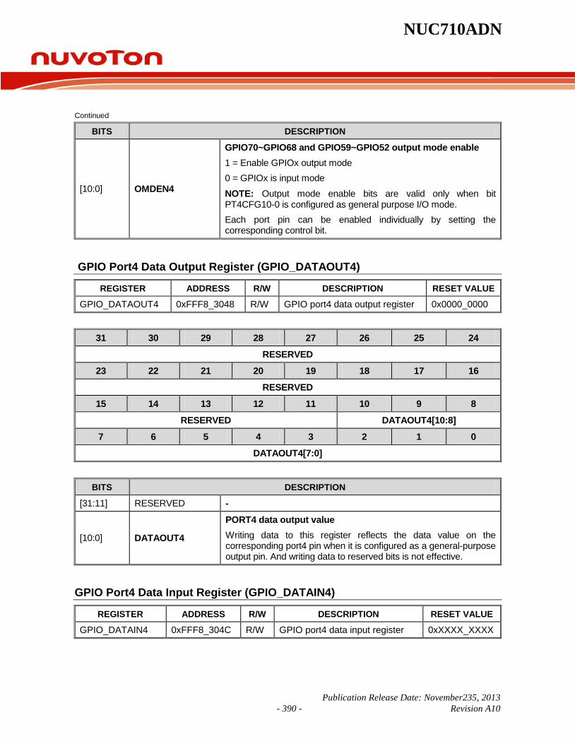
NUC710ADN
Publication Release Date: November235, 2013 - 390 - Revision A10
Continued
BITS DESCRIPTION
[10:0] OMDEN4
GPIO70~GPIO68 and GPIO59~GPIO52 output mode enable 1 = Enable GPIOx output mode 0 = GPIOx is input mode NOTE: Output mode enable bits are valid only when bit PT4CFG10-0 is configured as general purpose I/O mode. Each port pin can be enabled individually by setting the corresponding control bit.
GPIO Port4 Data Output Register (GPIO_DATAOUT4)
REGISTER ADDRESS R/W DESCRIPTION RESET VALUE
GPIO_DATAOUT4 0xFFF8_3048 R/W GPIO port4 data output register 0x0000_0000
31 30 29 28 27 26 25 24
RESERVED
23 22 21 20 19 18 17 16
RESERVED
15 14 13 12 11 10 9 8
RESERVED DATAOUT4[10:8]
7 6 5 4 3 2 1 0
DATAOUT4[7:0]
BITS DESCRIPTION
[31:11] RESERVED -
[10:0] DATAOUT4
PORT4 data output value Writing data to this register reflects the data value on the corresponding port4 pin when it is configured as a general-purpose output pin. And writing data to reserved bits is not effective.
GPIO Port4 Data Input Register (GPIO_DATAIN4)
REGISTER ADDRESS R/W DESCRIPTION RESET VALUE
GPIO_DATAIN4 0xFFF8_304C R/W GPIO port4 data input register 0xXXXX_XXXX
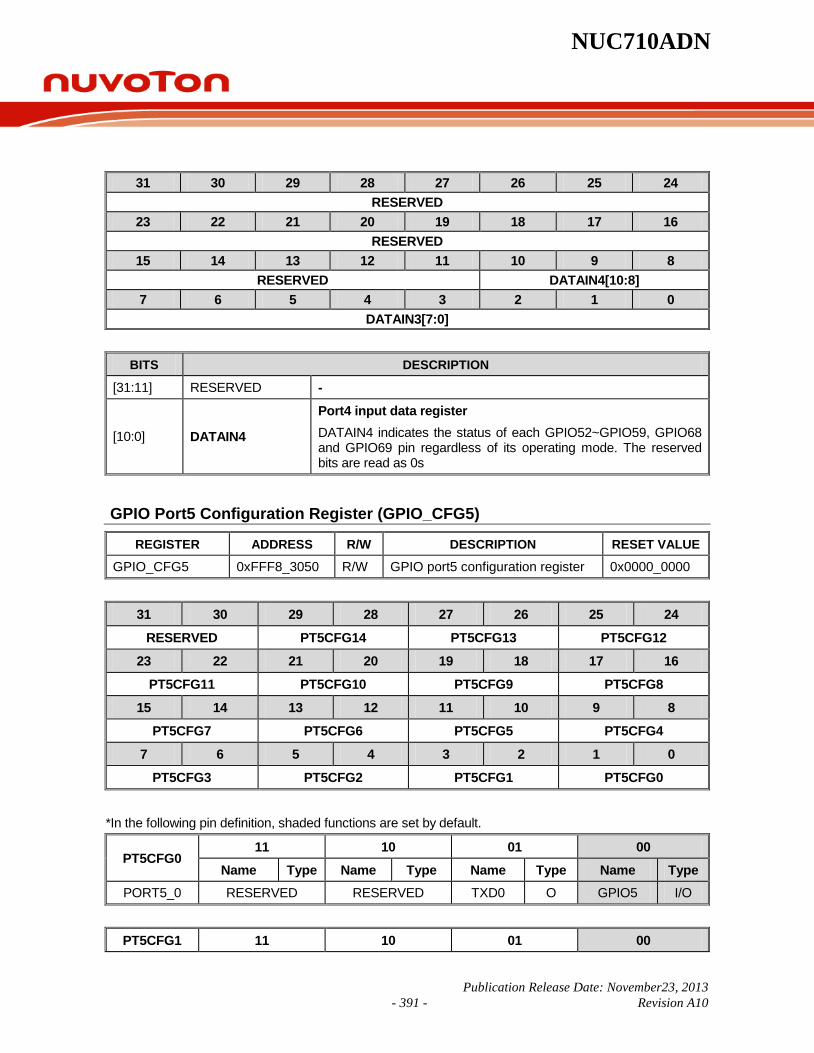
NUC710ADN
Publication Release Date: November23, 2013 - 391 - Revision A10
31 30 29 28 27 26 25 24 RESERVED
23 22 21 20 19 18 17 16 RESERVED
15 14 13 12 11 10 9 8 RESERVED DATAIN4[10:8]
7 6 5 4 3 2 1 0 DATAIN3[7:0]
BITS DESCRIPTION
[31:11] RESERVED -
[10:0] DATAIN4
Port4 input data register DATAIN4 indicates the status of each GPIO52~GPIO59, GPIO68 and GPIO69 pin regardless of its operating mode. The reserved bits are read as 0s
GPIO Port5 Configuration Register (GPIO_CFG5)
REGISTER ADDRESS R/W DESCRIPTION RESET VALUE
GPIO_CFG5 0xFFF8_3050 R/W GPIO port5 configuration register 0x0000_0000
31 30 29 28 27 26 25 24
RESERVED PT5CFG14 PT5CFG13 PT5CFG12
23 22 21 20 19 18 17 16
PT5CFG11 PT5CFG10 PT5CFG9 PT5CFG8
15 14 13 12 11 10 9 8
PT5CFG7 PT5CFG6 PT5CFG5 PT5CFG4
7 6 5 4 3 2 1 0
PT5CFG3 PT5CFG2 PT5CFG1 PT5CFG0
*In the following pin definition, shaded functions are set by default.
PT5CFG0 11 10 01 00
Name Type Name Type Name Type Name Type PORT5_0 RESERVED RESERVED TXD0 O GPIO5 I/O
PT5CFG1 11 10 01 00
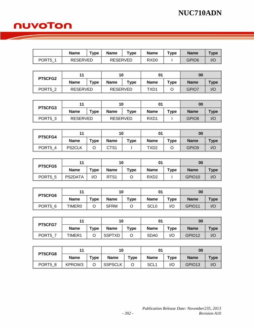
NUC710ADN
Publication Release Date: November235, 2013 - 392 - Revision A10
Name Type Name Type Name Type Name Type PORT5_1 RESERVED RESERVED RXD0 I GPIO6 I/O
PT5CFG2 11 10 01 00
Name Type Name Type Name Type Name Type PORT5_2 RESERVED RESERVED TXD1 O GPIO7 I/O
PT5CFG3 11 10 01 00
Name Type Name Type Name Type Name Type PORT5_3 RESERVED RESERVED RXD1 I GPIO8 I/O
PT5CFG4 11 10 01 00
Name Type Name Type Name Type Name Type PORT5_4 PS2CLK O CTS1 I TXD2 O GPIO9 I/O
PT5CFG5 11 10 01 00
Name Type Name Type Name Type Name Type PORT5_5 PS2DATA I/O RTS1 O RXD2 I GPIO10 I/O
PT5CFG6 11 10 01 00
Name Type Name Type Name Type Name Type PORT5_6 TIMER0 O SFRM O SCL0 I/O GPIO11 I/O
PT5CFG7 11 10 01 00
Name Type Name Type Name Type Name Type PORT5_7 TIMER1 O SSPTXD O SDA0 I/O GPIO12 I/O
PT5CFG8 11 10 01 00
Name Type Name Type Name Type Name Type PORT5_8 KPROW3 O SSPSCLK O SCL1 I/O GPIO13 I/O

NUC710ADN
Publication Release Date: November23, 2013 - 393 - Revision A10
PT5CFG9 11 10 01 00
Name Type Name Type Name Type Name Type PORT5_9 KPROW2 O SSPRXD I/O SDA1 I/O GPIO14 I/O
PT5CFG10 11 10 01 00
Name Type Name Type Name Type Name Type PORT5_10 RESERVED USBPWREN O nWDOG O GPIO15 I/O
PT5CFG11 11 10 01 00
Name Type Name Type Name Type Name Type PORT5_11 RESERVED RESERVED nIRQ0 I GPIO16 I/O
PT5CFG12 11 10 01 00
Name Type Name Type Name Type Name Type PORT5_12 RESERVED USBOVCUR I nIRQ1 I GPIO17 I/O
PT5CFG13 11 10 01 00
Name Type Name Type Name Type Name Type PORT5_13 RESERVED RESERVED nIRQ2 I GPIO18 I/O
PT5CFG14 11 10 01 00
Name Type Name Type Name Type Name Type PORT5_14 RESERVED RESERVED nIRQ3 I GPIO19 I/O
GPIO Port5 Direction Register (GPIO_DIR5)
REGISTER ADDRESS R/W DESCRIPTION RESET VALUE
GPIO_DIR5 0xFFF8_3054 R/W GPIO port5 in/out direction control and pull-up enable register 0x0000_0000

NUC710ADN
Publication Release Date: November235, 2013 - 394 - Revision A10
31 30 29 28 27 26 25 24
RESERVED PUPEN5[14:8]
23 22 21 20 19 18 17 16
PUPEN5[7:0]
15 14 13 12 11 10 9 8
RESERVED OMDEN5[14:8]
7 6 5 4 3 2 1 0
OMDEN5[7:0]
BITS DESCRIPTION [31] RESERVED -
[30:16] PUPEN5 GPIO19 ~ GPIO5 port pin internal pull-up resistor enable 1 = Enable pull-up resister 0 = Disable pull-up resister
[15] RESERVED -
[14:0] OUTEN5
GPIO19 ~ GPIO5 output mode enable 1 = Enable GPIOx output mode 0 = GPIOx is input mode NOTE: Output mode enable bits are valid only when bit PT5CFG9-0 is configured as general purpose I/O mode.Each port pin can be enabled individually by setting the corresponding control bit.
GPIO Port5 Data Output Register (GPIO_DATAOUT5)
REGISTER ADDRESS R/W DESCRIPTION RESET VALUE
GPIO_DATAOUT5 0xFFF8_3058 R/W GPIO port5 data output register 0x0000_0000
31 30 29 28 27 26 25 24
RESERVED
23 22 21 20 19 18 17 16
RESERVED
15 14 13 12 11 10 9 8
RESERVED DATAOUT5[14:8]
7 6 5 4 3 2 1 0
DATAOUT5[7:0]
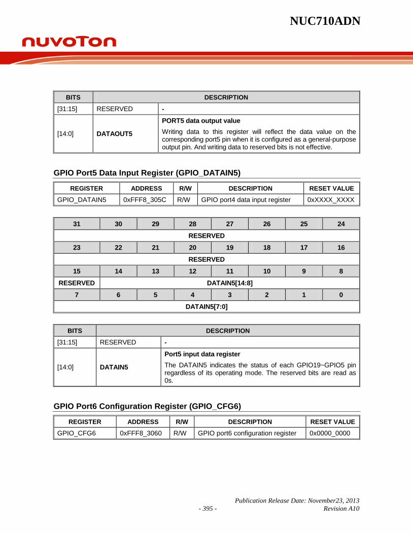
NUC710ADN
Publication Release Date: November23, 2013 - 395 - Revision A10
BITS DESCRIPTION
[31:15] RESERVED -
[14:0] DATAOUT5
PORT5 data output value Writing data to this register will reflect the data value on the corresponding port5 pin when it is configured as a general-purpose output pin. And writing data to reserved bits is not effective.
GPIO Port5 Data Input Register (GPIO_DATAIN5)
REGISTER ADDRESS R/W DESCRIPTION RESET VALUE
GPIO_DATAIN5 0xFFF8_305C R/W GPIO port4 data input register 0xXXXX_XXXX
31 30 29 28 27 26 25 24
RESERVED
23 22 21 20 19 18 17 16
RESERVED
15 14 13 12 11 10 9 8
RESERVED DATAIN5[14:8]
7 6 5 4 3 2 1 0
DATAIN5[7:0]
BITS DESCRIPTION
[31:15] RESERVED -
[14:0] DATAIN5
Port5 input data register The DATAIN5 indicates the status of each GPIO19~GPIO5 pin regardless of its operating mode. The reserved bits are read as 0s.
GPIO Port6 Configuration Register (GPIO_CFG6)
REGISTER ADDRESS R/W DESCRIPTION RESET VALUE
GPIO_CFG6 0xFFF8_3060 R/W GPIO port6 configuration register 0x0000_0000
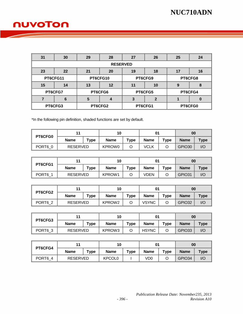
NUC710ADN
Publication Release Date: November235, 2013 - 396 - Revision A10
31 30 29 28 27 26 25 24
RESERVED
23 22 21 20 19 18 17 16
PT6CFG11 PT6CFG10 PT6CFG9 PT6CFG8
15 14 13 12 11 10 9 8
PT6CFG7 PT6CFG6 PT6CFG5 PT6CFG4
7 6 5 4 3 2 1 0
PT6CFG3 PT6CFG2 PT6CFG1 PT6CFG0
*In the following pin definition, shaded functions are set by default.
PT6CFG0 11 10 01 00
Name Type Name Type Name Type Name Type PORT6_0 RESERVED KPROW0 O VCLK O GPIO30 I/O
PT6CFG1 11 10 01 00
Name Type Name Type Name Type Name Type PORT6_1 RESERVED KPROW1 O VDEN O GPIO31 I/O
PT6CFG2 11 10 01 00
Name Type Name Type Name Type Name Type PORT6_2 RESERVED KPROW2 O VSYNC O GPIO32 I/O
PT6CFG3 11 10 01 00
Name Type Name Type Name Type Name Type PORT6_3 RESERVED KPROW3 O HSYNC O GPIO33 I/O
PT6CFG4 11 10 01 00
Name Type Name Type Name Type Name Type PORT6_4 RESERVED KPCOL0 I VD0 O GPIO34 I/O
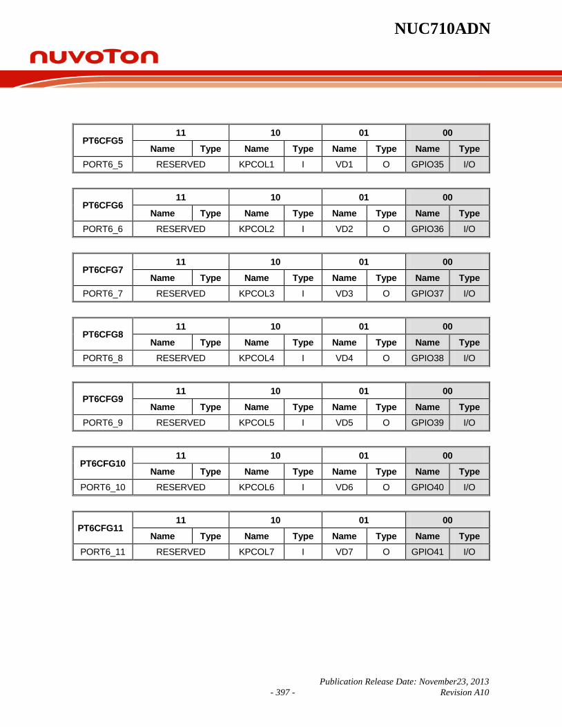
NUC710ADN
Publication Release Date: November23, 2013 - 397 - Revision A10
PT6CFG5 11 10 01 00
Name Type Name Type Name Type Name Type PORT6_5 RESERVED KPCOL1 I VD1 O GPIO35 I/O
PT6CFG6 11 10 01 00
Name Type Name Type Name Type Name Type PORT6_6 RESERVED KPCOL2 I VD2 O GPIO36 I/O
PT6CFG7 11 10 01 00
Name Type Name Type Name Type Name Type PORT6_7 RESERVED KPCOL3 I VD3 O GPIO37 I/O
PT6CFG8 11 10 01 00
Name Type Name Type Name Type Name Type PORT6_8 RESERVED KPCOL4 I VD4 O GPIO38 I/O
PT6CFG9 11 10 01 00
Name Type Name Type Name Type Name Type PORT6_9 RESERVED KPCOL5 I VD5 O GPIO39 I/O
PT6CFG10 11 10 01 00
Name Type Name Type Name Type Name Type PORT6_10 RESERVED KPCOL6 I VD6 O GPIO40 I/O
PT6CFG11 11 10 01 00
Name Type Name Type Name Type Name Type PORT6_11 RESERVED KPCOL7 I VD7 O GPIO41 I/O

NUC710ADN
Publication Release Date: November235, 2013 - 398 - Revision A10
GPIO Port6 Direction Register (GPIO_DIR6)
REGISTER ADDRESS R/W DESCRIPTION RESET VALUE
GPIO_DIR6 0xFFF8_3064 R/W GPIO port5 in/out direction control and pull-up enable register 0x0000_0000
31 30 29 28 27 26 25 24
RESERVED PUPEN6[11:8]
23 22 21 20 19 18 17 16
PUPEN6[7:0]
15 14 13 12 11 10 9 8
RESERVED OMDEN6[11:8]
7 6 5 4 3 2 1 0
OMDEN6[7:0]
BITS DESCRIPTION [31:27] RESERVED -
[26:16] PUPEN6 GPIO30 ~GPIO41 port pin internal pull-up resistor enable 1 = Enable pull-up resister 0 = Disable pull-up resister
[15:13] RESERVED
[12:0] OMDEN6
GPIO41 ~ GPIO30 output mode enable 1 = Enable GPIOx output mode 0 = GPIOx is input mode NOTE: Output mode enable bits are valid only when bit PT6CFG11-0 is configured as general purpose I/O mode. Each port pin can be enabled individually by setting the corresponding control bit.
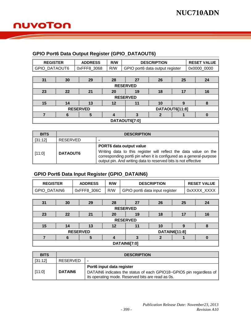
NUC710ADN
Publication Release Date: November23, 2013 - 399 - Revision A10
GPIO Port6 Data Output Register (GPIO_DATAOUT6) REGISTER ADDRESS R/W DESCRIPTION RESET VALUE
GPIO_DATAOUT6 0xFFF8_3068 R/W GPIO port6 data output register 0x0000_0000
31 30 29 28 27 26 25 24 RESERVED
23 22 21 20 19 18 17 16 RESERVED
15 14 13 12 11 10 9 8 RESERVED DATAOUT6[11:8]
7 6 5 4 3 2 1 0 DATAOUT6[7:0]
BITS DESCRIPTION
[31:12] RESERVED -
[11:0] DATAOUT6
PORT6 data output value Writing data to this register will reflect the data value on the corresponding port6 pin when it is configured as a general-purpose output pin. And writing data to reserved bits is not effective
GPIO Port6 Data Input Register (GPIO_DATAIN6)
REGISTER ADDRESS R/W DESCRIPTION RESET VALUE
GPIO_DATAIN6 0xFFF8_306C R/W GPIO port6 data input register 0xXXXX_XXXX
31 30 29 28 27 26 25 24 RESERVED
23 22 21 20 19 18 17 16 RESERVED
15 14 13 12 11 10 9 8 RESERVED DATAIN6[11:8]
7 6 5 4 3 2 1 0 DATAIN6[7:0]
BITS DESCRIPTION [31:12] RESERVED -
[11:0] DATAIN6 Port6 input data register DATAIN6 indicates the status of each GPIO18~GPIO5 pin regardless of its operating mode. Reserved bits are read as 0s.

NUC710ADN
Publication Release Date: November235, 2013 - 400 - Revision A10
GPIO Debounce Control Register (GPIO_DBNCECON)
REGISTER ADDRESS R/W DESCRIPTION RESET VALUE
GPIO_DBNCECON 0xFFF8_3070 R/W GPIO debounce control register 0xXXXX_XX00
31 30 29 28 27 26 25 24
RESERVED
23 22 21 20 19 18 17 16
RESERVED
15 14 13 12 11 10 9 8
RESERVED
7 6 5 4 3 2 1 0
RESERVED DBCLKSEL DBEN3 DBEN2 DBEN1 DBEN0
BITS DESCRIPTION
[31:7] RESERVED -
[6:4] DBCLKSEL
Debounce Clock Selection These 3 bits are used to select the clock rate for the debounce circuit. The relationship between the system clock HCLK and the debounce clock TCLK_BUN is as follows: TCLK _BUN = HCLK / 2DBCLKSEL
[3] DBEN3 Debounce circuit enable for GPIO19 (nIRQ3) 1 = Enable GPIO19 debounce function 0 = Disable GPIO19 debounce function
[2] DBEN2 Debounce circuit enable for GPIO18 (nIRQ2) 1 = Enable GPIO18 debounce function 0 = Disable GPIO18 debounce function
[1] DBEN1 Debounce circuit enable for GPIO17 (nIRQ1) 1 = Enable GPIO17 debounce function 0 = Disable GPIO17 debounce function
[0] DBEN0 Debounce circuit enable for GPIO16 (nIRQ0) 1 = Enable GPIO16 debounce function 0 = Disable GPIO16 debounce function
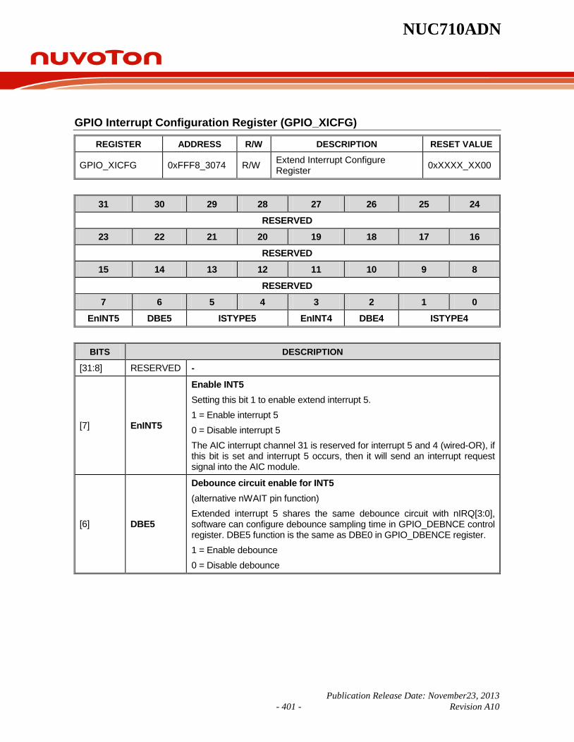
NUC710ADN
Publication Release Date: November23, 2013 - 401 - Revision A10
GPIO Interrupt Configuration Register (GPIO_XICFG)
REGISTER ADDRESS R/W DESCRIPTION RESET VALUE
GPIO_XICFG 0xFFF8_3074 R/W Extend Interrupt Configure Register 0xXXXX_XX00
31 30 29 28 27 26 25 24
RESERVED
23 22 21 20 19 18 17 16
RESERVED
15 14 13 12 11 10 9 8
RESERVED
7 6 5 4 3 2 1 0
EnINT5 DBE5 ISTYPE5 EnINT4 DBE4 ISTYPE4
BITS DESCRIPTION
[31:8] RESERVED -
[7] EnINT5
Enable INT5 Setting this bit 1 to enable extend interrupt 5. 1 = Enable interrupt 5 0 = Disable interrupt 5 The AIC interrupt channel 31 is reserved for interrupt 5 and 4 (wired-OR), if this bit is set and interrupt 5 occurs, then it will send an interrupt request signal into the AIC module.
[6] DBE5
Debounce circuit enable for INT5 (alternative nWAIT pin function) Extended interrupt 5 shares the same debounce circuit with nIRQ[3:0], software can configure debounce sampling time in GPIO_DEBNCE control register. DBE5 function is the same as DBE0 in GPIO_DBENCE register. 1 = Enable debounce 0 = Disable debounce

NUC710ADN
Publication Release Date: November235, 2013 - 402 - Revision A10
Continued
BITS DESCRIPTION
[5:4] STYPE5
Interrupt 5 source type
ISTYPE5 Interrupt Source Type 2’b00 LOW level sensitive
2’b01 HIGH level sensitive
2’b10 Negative edge triggered
2’b11 Positive edge triggered
[3] EnINT4
Enable INT4 Setting this bit to 1 enables extended interrupt 4 1 = Enable interrupt 4 0 = Disable interrupt 4 AIC interrupt channel 31 is reserved for interrupt 5 and 4 (wire-OR), if this bit is set and interrupt 4 occurs, then it will send an interrupt request signal into AIC module.
[2] DBE4
Debounce circuit enable for INT4 (GPIO0 pin alternative function) 1 = Enable debounce 0 = Disable debounce Extended interrupt 4 shares the same debounce circuit with nIRQ[3:0], software and can configure debounce sampling time in GPIO_DEBNCE control register. DBE5 function is the same as DBE0 in GPIO_DBENCE register.
[1:0] ISTYPE4
Interrupt 4 source type
ISTYPE5 Interrupt Source Type 2’b00 LOW level sensitive 2’b01 HIGH level sensitive 2’b10 Negative edge triggered 2’b11 Positive edge triggered

NUC710ADN
Publication Release Date: November23, 2013 - 403 - Revision A10
GPIO Interrupt Status Register (GPIO_XISTATUS)
REGISTER ADDRESS R/W DESCRIPTION RESET VALUE
GPIO_XISTATUS 0xFFF8_3078 R/W Extend interrupt status (flag) register 0xXXXX_XX00
31 30 29 28 27 26 25 24
RESERVED
23 22 21 20 19 18 17 16
RESERVED
15 14 13 12 11 10 9 8
RESERVED
7 6 5 4 3 2 1 0
RESERVED INT5 INT4
BITS DESCRIPTION
[31:2] RESERVED -
[1] INT5
Interrupt 5 status When an interrupt input is detected with ISTYPE5 triggered condition, this flag is set. It must be cleared by software. 1 = interrupt detected. 0 = No interrupt
[0] INT4
Interrupt 4 status When interrupt input is detected with ISTYPE4 triggered condition, this flag is set. It must be cleared by software. 1 = interrupt 4 is detected. 0 = no interrupt

NUC710ADN
Publication Release Date: November235, 2013 - 404 - Revision A10
6.16 Real Time Clock The Real Time Clock (RTC) block can be operated by an independent power supply while the system power is off. The RTC block utilizes an external crystal to generate 32.768 KHz clock. The RTC can transmit data to the CPU as BCD values. The data includes the time by second, minute, hour and the date by day, month, and year. In addition, to reach better frequency accuracy, the RTC counter can be adjusted by software. RTC features are shown as below: Timer counter (second, minute, hour) and calendar counter (day, month, year). Alarm register (second, minute, hour, day, month, year). 12/24-hour mode selectable. Recognize leap year automatically. Weekday counter. Frequency compensate register (RTC_FCR). Beside RTC_FCR, all clock and alarm data expressed in BCD code. Support two kinds of interrupt ( tick and alarm) RTC Initiation: When RTC block is powered on, programmer has to write a number (0xa5eb1357) to RTC_INIR to reset all logic. RTC_INIR act as hardware reset circuit. Once RTC_INIR has been set as 0xa5eb1357, user cannot reload any other value. RTC write enable: Register RTC_AER bit 15~0 is RTC read /write password. It is used to avoid signal interference from the system during system power off. RTC_AER bit 15~0 has to be set as 0xa965 before the user can write new data to all registers besides RTC_INIR. If the user set RTC_AER as 0xa965, RTC_WRITE_EN is raised high. Then the user can feel free to write data to the register. RTC_WRITE_EN will keep high for a short period (about 24ms) and it is automatically pulled low by internal state machine. Frequency Compensation: The RTC_FCR allows software controlled digital compensation of a 32.768 KHz crystal oscillator. User can utilize a frequency counter to measure the RTC clock in one of the GPIO pins during manufacture, and store the value in Flash memory for retrieval when the product is first power on. Time and Calendar counter: RTC_TLR and RTC_CLR are used to load the time and calendar. RTC_TAR and RTC_CAR are used as alarm. They are all BCD counters. 12/24 hour Time scale selection: The 12/24 hour time scale selection depends on RTC_TSSR bit 0.
Weekday counter: Counts from Sunday to Saturday
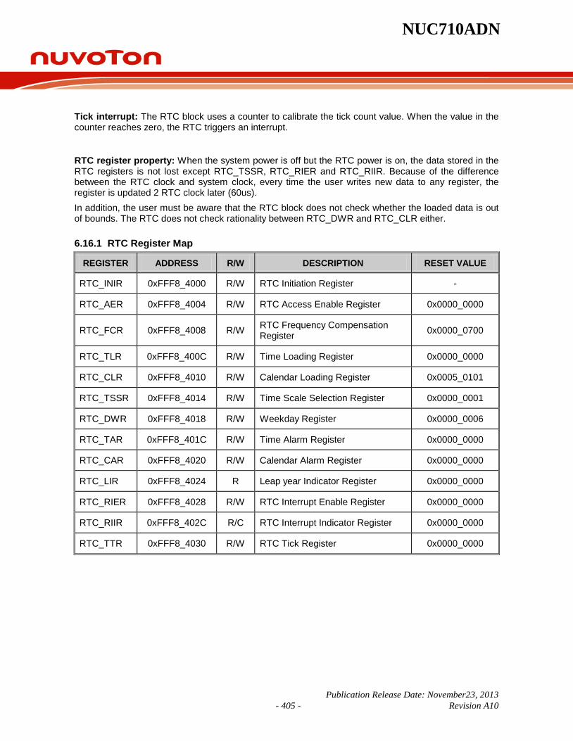
NUC710ADN
Publication Release Date: November23, 2013 - 405 - Revision A10
Tick interrupt: The RTC block uses a counter to calibrate the tick count value. When the value in the counter reaches zero, the RTC triggers an interrupt.
RTC register property: When the system power is off but the RTC power is on, the data stored in the RTC registers is not lost except RTC_TSSR, RTC_RIER and RTC_RIIR. Because of the difference between the RTC clock and system clock, every time the user writes new data to any register, the register is updated 2 RTC clock later (60us). In addition, the user must be aware that the RTC block does not check whether the loaded data is out of bounds. The RTC does not check rationality between RTC_DWR and RTC_CLR either.
6.16.1 RTC Register Map
REGISTER ADDRESS R/W DESCRIPTION RESET VALUE
RTC_INIR 0xFFF8_4000 R/W RTC Initiation Register -
RTC_AER 0xFFF8_4004 R/W RTC Access Enable Register 0x0000_0000
RTC_FCR 0xFFF8_4008 R/W RTC Frequency Compensation Register 0x0000_0700
RTC_TLR 0xFFF8_400C R/W Time Loading Register 0x0000_0000
RTC_CLR 0xFFF8_4010 R/W Calendar Loading Register 0x0005_0101
RTC_TSSR 0xFFF8_4014 R/W Time Scale Selection Register 0x0000_0001
RTC_DWR 0xFFF8_4018 R/W Weekday Register 0x0000_0006
RTC_TAR 0xFFF8_401C R/W Time Alarm Register 0x0000_0000
RTC_CAR 0xFFF8_4020 R/W Calendar Alarm Register 0x0000_0000
RTC_LIR 0xFFF8_4024 R Leap year Indicator Register 0x0000_0000
RTC_RIER 0xFFF8_4028 R/W RTC Interrupt Enable Register 0x0000_0000
RTC_RIIR 0xFFF8_402C R/C RTC Interrupt Indicator Register 0x0000_0000
RTC_TTR 0xFFF8_4030 R/W RTC Tick Register 0x0000_0000

NUC710ADN
Publication Release Date: November235, 2013 - 406 - Revision A10
RTC Initiation Register (RTC_INIR)
REGISTER ADDRESS R/W DESCRIPTION RESET VALUE
RTC_INIR 0xFFF8_4000 R/W RTC Initiation Register -
31 30 29 28 27 26 25 24 INIR[31:24]
23 22 21 20 19 18 17 16 INIR[23:16]
15 14 13 12 11 10 9 8 INIR[15:8]
7 6 5 4 3 2 1 0 INIR[7:0]
BITS DESCRIPTIONS
[31:0] INIR
INIR [31:0]: The INIR register is used to replace the hardware reset circuit. Programmer must write INIR as “0xa5eb_1357” after RTC is powered. INIR [0]: R/W. Once the RTC INIR is written, the user can access this bit to find out whether the RTC reset signal was pulled high.
RTC Access Enable Register (RTC_AER)
REGISTER ADDRESS R/W DESCRIPTION RESET VALUE
RTC_AER 0xFFF8_4004 R/W RTC Access Enable Register 0X0000_0000
31 30 29 28 27 26 25 24 Reserved
23 22 21 20 19 18 17 16 Reserved AER[16]
15 14 13 12 11 10 9 8 AER[15:8]
7 6 5 4 3 2 1 0 AER[7:0]

NUC710ADN
Publication Release Date: November23, 2013 - 407 - Revision A10
BITS DESCRIPTIONS
[31:17] Reserved -
[16:0] AER
AER [16]: Read only 1 = RTC register write enable 0 = RTC register write disable AER[15:0]: Write only RTC register write enable/disable password 0xa965 = Write enable 0x0000 = Write disable
RTC Frequency Compensation Register (RTC_FCR)
REGISTER ADDRESS R/W DESCRIPTION RESET VALUE
RTC_FCR 0xFFF8_4008 R/W RTC Frequency Compensation Register 0x0000_0700
31 30 29 28 27 26 25 24
Reserved
23 22 21 20 19 18 17 16
Reserved
15 14 13 12 11 10 9 8
Reserved FCR_int
7 6 5 4 3 2 1 0
Reserved FCR_fra
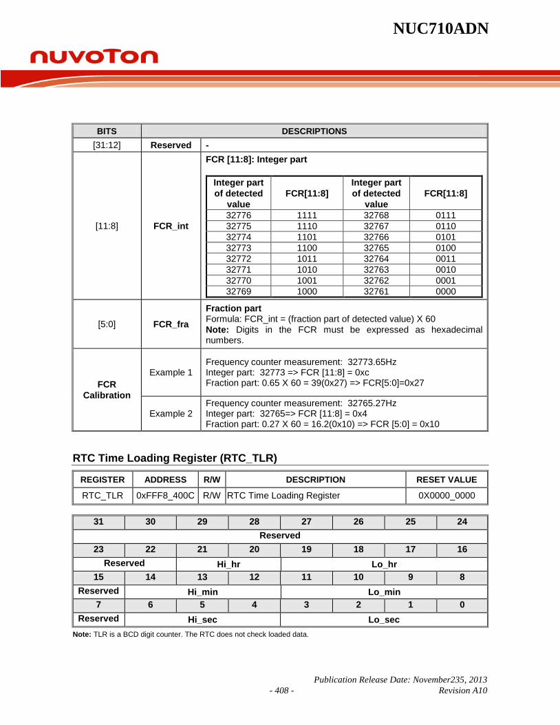
NUC710ADN
Publication Release Date: November235, 2013 - 408 - Revision A10
BITS DESCRIPTIONS [31:12] Reserved -
[11:8] FCR_int
FCR [11:8]: Integer part
Integer part of detected
value FCR[11:8]
Integer part of detected
value FCR[11:8]
32776 1111 32768 0111 32775 1110 32767 0110 32774 1101 32766 0101 32773 1100 32765 0100 32772 1011 32764 0011 32771 1010 32763 0010 32770 1001 32762 0001 32769 1000 32761 0000
[5:0] FCR_fra
Fraction part Formula: FCR_int = (fraction part of detected value) X 60 Note: Digits in the FCR must be expressed as hexadecimal numbers.
FCR Calibration
Example 1 Frequency counter measurement: 32773.65Hz Integer part: 32773 => FCR [11:8] = 0xc Fraction part: 0.65 X 60 = 39(0x27) => FCR[5:0]=0x27
Example 2 Frequency counter measurement: 32765.27Hz Integer part: 32765=> FCR [11:8] = 0x4 Fraction part: 0.27 X 60 = 16.2(0x10) => FCR [5:0] = 0x10
RTC Time Loading Register (RTC_TLR)
REGISTER ADDRESS R/W DESCRIPTION RESET VALUE
RTC_TLR 0xFFF8_400C R/W RTC Time Loading Register 0X0000_0000
31 30 29 28 27 26 25 24 Reserved
23 22 21 20 19 18 17 16 Reserved Hi_hr Lo_hr
15 14 13 12 11 10 9 8 Reserved Hi_min Lo_min
7 6 5 4 3 2 1 0 Reserved Hi_sec Lo_sec
Note: TLR is a BCD digit counter. The RTC does not check loaded data.

NUC710ADN
Publication Release Date: November23, 2013 - 409 - Revision A10
BITS DESCRIPTIONS
[21:20] Hi_hr 10 hour time digit
[19:16] Lo_hr 1 hour time digit
[14:12] Hi_min 10 min time digit
[11:8] Lo_min 1 min time digit
[6:4] Hi_sec 10 sec time digit
[3:0] Lo_sec 1 sec time digit
RTC Calendar Loading Register (RTC_CLR)
REGISTER ADDRESS R/W DESCRIPTION RESET VALUE
RTC_CLR 0xFFF8_4010 R/W RTC Calendar Loading Register 0X0005_0101
31 30 29 28 27 26 25 24
Reserved
23 22 21 20 19 18 17 16
Hi_year Lo_year
15 14 13 12 11 10 9 8
Reserved Hi_mon Lo_mon
7 6 5 4 3 2 1 0
Reserved Hi_day Lo_day
Note: CLR is a BCD digit counter. The RTC does not check loaded data
BITS DESCRIPTIONS
[23:20] Hi_year 10-year calendar digit
[19:16] Lo_year 1-year calendar digit
[12] Hi_mon 10-month calendar digit
[11:8] Lo_mon 1-month calendar digit
[5:4] Hi_day 10-day calendar digit
[3:0] Lo_day 1-day calendar digit

NUC710ADN
Publication Release Date: November235, 2013 - 410 - Revision A10
RTC Time Scale Selection Register (RTC_TSSR)
REGISTER ADDRESS R/W DESCRIPTION RESET VALUE
RTC_TSSR 0xFFF8_40014 R/W Time Scale Selection Register 0X0000_0001
31 30 29 28 27 26 25 24 Reserved
23 22 21 20 19 18 17 16 Reserved
15 14 13 12 11 10 9 8 Reserved
7 6 5 4 3 2 1 0 Reserved 24Hr/12Hr
BITS DESCRIPTIONS
[31:1] Reserved -
[0] 24Hr/12Hr
24Hr/12Hr: 24hour / 12 hour mode selection Indicates that TLR and TAR are in 24-hour mode or 12-hour mode 1 = Select 24-hour time scale 0 = Select 12-hour time scale with am and pm indication
24-hour time scale
12-hour time scale
24-hour time scale
12-hour time scale
00 12(AM12) 12 32(PM12) 01 01(AM01) 13 21(PM01) 02 02(AM02) 14 22(PM02) 03 03(AM03) 15 23(PM03) 04 04(AM04) 16 24(PM04) 05 05(AM05) 17 25(PM05) 06 06(AM06) 18 26(PM06) 07 07(AM07) 19 27(PM07) 08 08(AM08) 20 28(PM08) 09 09(AM09) 21 29(PM09) 10 10(AM10) 22 30(PM10) 11 11(AM11) 23 31(PM11)
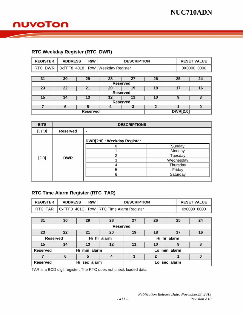
NUC710ADN
Publication Release Date: November23, 2013 - 411 - Revision A10
RTC Weekday Register (RTC_DWR)
REGISTER ADDRESS R/W DESCRIPTION RESET VALUE
RTC_DWR 0xFFF8_4018 R/W Weekday Register 0X0000_0006
31 30 29 28 27 26 25 24 Reserved
23 22 21 20 19 18 17 16 Reserved
15 14 13 12 11 10 9 8 Reserved
7 6 5 4 3 2 1 0 Reserved DWR[2:0]
BITS DESCRIPTIONS
[31:3] Reserved -
[2:0] DWR
DWR[2:0] : Weekday Register 0 Sunday 1 Monday 2 Tuesday 3 Wednesday 4 Thursday 5 Friday 6 Saturday
RTC Time Alarm Register (RTC_TAR)
REGISTER ADDRESS R/W DESCRIPTION RESET VALUE
RTC_TAR 0xFFF8_401C R/W RTC Time Alarm Register 0x0000_0000
31 30 29 28 27 26 25 24 Reserved
23 22 21 20 19 18 17 16 Reserved Hi_hr_alarm Hi_hr_alarm
15 14 13 12 11 10 9 8 Reserved Hi_min_alarm Lo_min_alarm
7 6 5 4 3 2 1 0 Reserved Hi_sec_alarm Lo_sec_alarm
TAR is a BCD digit register. The RTC does not check loaded data
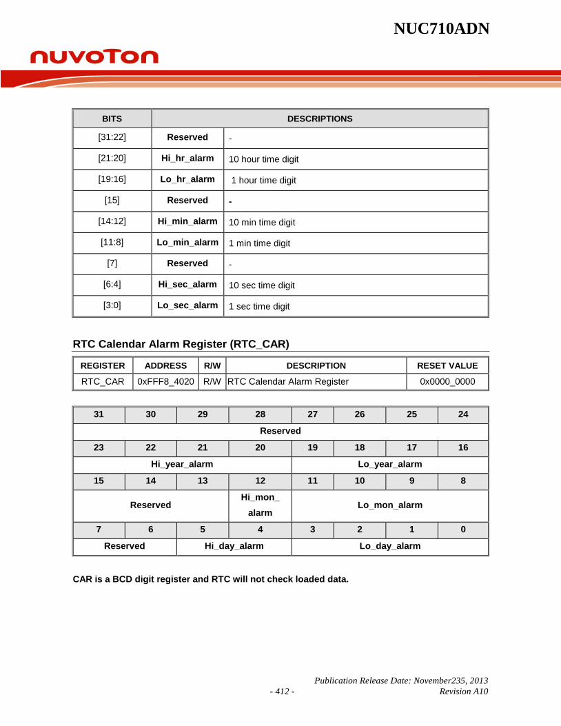
NUC710ADN
Publication Release Date: November235, 2013 - 412 - Revision A10
BITS DESCRIPTIONS
[31:22] Reserved -
[21:20] Hi_hr_alarm 10 hour time digit
[19:16] Lo_hr_alarm 1 hour time digit
[15] Reserved -
[14:12] Hi_min_alarm 10 min time digit
[11:8] Lo_min_alarm 1 min time digit
[7] Reserved -
[6:4] Hi_sec_alarm 10 sec time digit
[3:0] Lo_sec_alarm 1 sec time digit
RTC Calendar Alarm Register (RTC_CAR)
REGISTER ADDRESS R/W DESCRIPTION RESET VALUE
RTC_CAR 0xFFF8_4020 R/W RTC Calendar Alarm Register 0x0000_0000
31 30 29 28 27 26 25 24
Reserved
23 22 21 20 19 18 17 16
Hi_year_alarm Lo_year_alarm
15 14 13 12 11 10 9 8
Reserved Hi_mon_
alarm Lo_mon_alarm
7 6 5 4 3 2 1 0
Reserved Hi_day_alarm Lo_day_alarm
CAR is a BCD digit register and RTC will not check loaded data.

NUC710ADN
Publication Release Date: November23, 2013 - 413 - Revision A10
BITS DESCRIPTIONS
[31:24] Reserved -
[23:20] Hi_year 10-year calendar digit
[19:16] Lo_year 1-year calendar digit
[15:13] Reserved -
[12] Hi_mon 10-month calendar digit
[11:8] Lo_mon 1-month calendar digit
[5:4] Hi_day 10-day calendar digit
[3:0] Lo_day 1-day calendar digit
RTC Leap year Indication Register (RTC_LIR)
REGISTER ADDRESS R/W DESCRIPTION RESET VALUE
RTC_LIR 0xFFF8_4024 R RTC Leap year Indication Register 0X0000_0000
31 30 29 28 27 26 25 24
Reserved
23 22 21 20 19 18 17 16
Reserved
15 14 13 12 11 10 9 8
Reserved
7 6 5 4 3 2 1 0
Reserved LIR[0]
BITS DESCRIPTIONS
[31:1] Reserved -
[0] LIR LIR [0]: Real only. Leap year Indication 1 = Indicates this year is a leap year 0 = Indicates this year is not a leap year
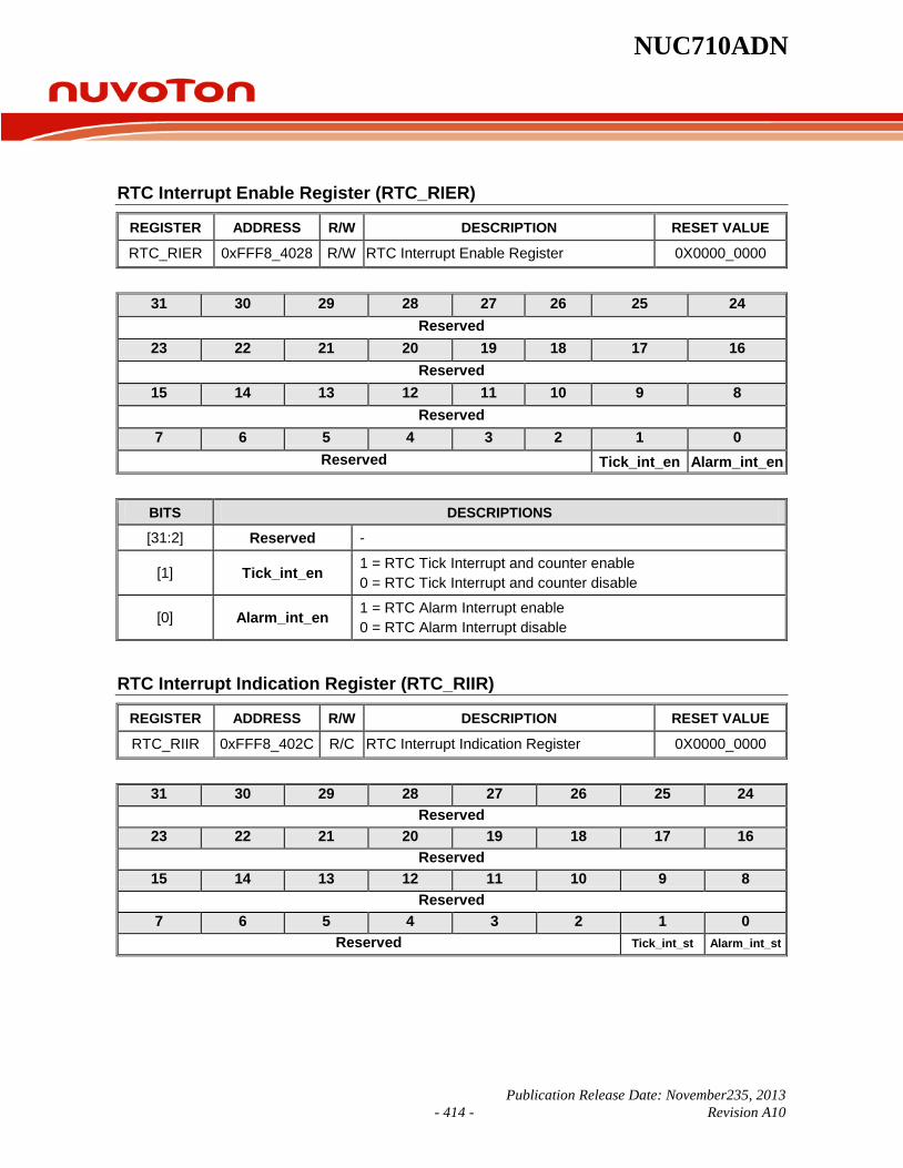
NUC710ADN
Publication Release Date: November235, 2013 - 414 - Revision A10
RTC Interrupt Enable Register (RTC_RIER)
REGISTER ADDRESS R/W DESCRIPTION RESET VALUE
RTC_RIER 0xFFF8_4028 R/W RTC Interrupt Enable Register 0X0000_0000
31 30 29 28 27 26 25 24 Reserved
23 22 21 20 19 18 17 16 Reserved
15 14 13 12 11 10 9 8 Reserved
7 6 5 4 3 2 1 0 Reserved Tick_int_en Alarm_int_en
BITS DESCRIPTIONS
[31:2] Reserved -
[1] Tick_int_en 1 = RTC Tick Interrupt and counter enable 0 = RTC Tick Interrupt and counter disable
[0] Alarm_int_en 1 = RTC Alarm Interrupt enable 0 = RTC Alarm Interrupt disable
RTC Interrupt Indication Register (RTC_RIIR)
REGISTER ADDRESS R/W DESCRIPTION RESET VALUE
RTC_RIIR 0xFFF8_402C R/C RTC Interrupt Indication Register 0X0000_0000
31 30 29 28 27 26 25 24 Reserved
23 22 21 20 19 18 17 16 Reserved
15 14 13 12 11 10 9 8 Reserved
7 6 5 4 3 2 1 0 Reserved Tick_int_st Alarm_int_st

NUC710ADN
Publication Release Date: November23, 2013 - 415 - Revision A10
BITS DESCRIPTIONS
[31:2] Reserved -
[1] Tick_int_st RTC Tick Interrupt Indication REGISTER 1 = Indicates the time tick interrupt has been activated. 0 = Indicates the tick interrupt did not occur.
[0] Alarm_int_st
RTC Alarm Interrupt Indication 1 = Indicates the timer and calendar counter have counted to a specified time recorded in TAR and CAR. The RTC alarm interrupt is triggered. 0 = Indicates the alarm interrupt did not occur.
Note : User can clear these two bits by writing 0x0 to RIIR
RTC Tick Time Register (RTC_TTR)
REGISTER ADDRESS R/W DESCRIPTION RESET VALUE
RTC_TTR 0xFFF8_4030 R/W RTC Tick Register 0x0000_0000
31 30 29 28 27 26 25 24
Reserved
23 22 21 20 19 18 17 16
Reserved
15 14 13 12 11 10 9 8
Reserved
7 6 5 4 3 2 1 0
Reserved TTI
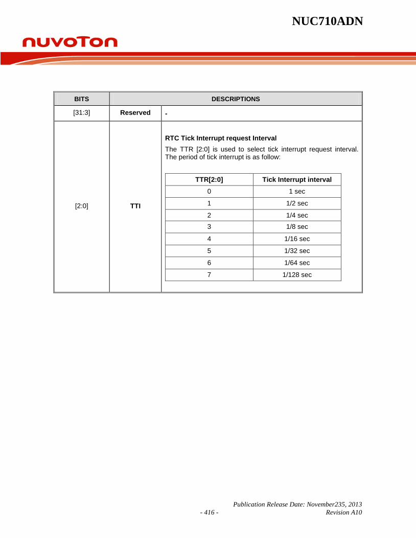
NUC710ADN
Publication Release Date: November235, 2013 - 416 - Revision A10
BITS DESCRIPTIONS
[31:3] Reserved -
[2:0] TTI
RTC Tick Interrupt request Interval The TTR [2:0] is used to select tick interrupt request interval. The period of tick interrupt is as follow:
TTR[2:0] Tick Interrupt interval 0 1 sec
1 1/2 sec
2 1/4 sec
3 1/8 sec
4 1/16 sec
5 1/32 sec
6 1/64 sec
7 1/128 sec

NUC710ADN
Publication Release Date: November23, 2013 - 417 - Revision A10
6.16.2 RTC Application Note
Detect RTC frequency
Step1. Configure GPIO register GPIOCFG5 [21:20] as “2’b11” Step2. Making use of the frequency counter (for example: Agilent 53131A) to detect NUC710 IO Pin “GPIO15/nWDOG/USBPWREN”. Note: Because the parasitic capacitance would slow crystal oscillation, do not connect the probe with 32K crystal directly.
RTC application circuit
1. The recommended RTC application circuit is as follows:
EXTAL32
XTAL32
RTCVDD1.8V
C1
C2
2. C1 and C2 cannot be connected to ground for improving the noise issue. 3. Do not connect any resister in the circuit. Redundant resister may stop crystal oscillation. 4. To avoid parasitic capacitance and resistance, the user should place all components as close as
possible. 5. The C1 and C2 value can be changed with different crystals because different crystals require
different oscillation conditions. In general, the capacitance value of C1/C2 is between 10pF and 30pF.

NUC710ADN
Publication Release Date: November235, 2013 - 418 - Revision A10
6.17 Smart Card Host Interface The Smart Card resides in APB bus. Smart Card Interface port pins in NUC710 that operates at 3.3V with 5V input tolerance, the smart card can interface to NUC710 directly regardless it output high is 5v or 3v.. Advanced power management features further optimize power consumption whether during operation or powering down.
ISO-7816 compliant PC/SC T=0, T=1 compliant 16-byte transmitter FIFO and 16-byte receiver FIFO FIFO threshold interrupt to optimize system performance
Programmable transmission clock frequency Versatile baud rate configuration UART-like register file structure Versatile 8-bit, 16-bit, 24-bit timer for Answer-To-Reset (ATR) and processing wait-times. Parity error counters during reception mode and in transmission mode with automatic re-
transmission. Automatic activation and deactivation sequence through an independence sequencer
6.17.1 Register Mapping R: read only, W: write only, R/W: both read and write, C: Only value 0 can be written.
Table 6.12.2.1 Smart Card Host Interface 0 Register Map
REGISTER ADDRESS R/W DESCRIPTION RESET VALUE
Smartcard Host Interface 0 SCHI_RBR0 0xFFF8_5000 (BDLAB=0) R Receiver Buffer Register Undefined SCHI_TBR0 0xFFF8_5000 (BDLAB=0) W Transmitter Buffer Register Undefined SCHI_IER0 0xFFF8_5004 (BDLAB=0) R/W Interrupt Enable Register 0x0000_0080 SCHI_ISR0 0xFFF8_5008 (BDLAB=0) R Interrupt Status Register 0X0000_00C1 SCHI_SCFR0 0xFFF8_5008 (BDLAB=0) W Smart card FIFO Control Register 0x0000_0000 SCHI_SCCR0 0xFFF8_500C R/W Smart card Control Register 0x0000_0018 SCHI_CBR0 0xFFF8_5010 R/W Clock Base Register 0x0000_000C SCHI_SCSR0 0xFFF8_5014 R Smart Card Status Register 0x0000_0060 SCHI_GTR0 0xFFF8_5018 R/W Guard Rime Register 0x0000_0001 SCHI_ECR0 0xFFF8_501C R/W Extended Control Register 0x0000_0052 SCHI_TMR0 0xFFF8_5020 R/W Test Mode Register 0x0000_0000 SCHI_TOC0 0xFFF8_5028 R/W Time out Configuration Register 0x0000_0000

NUC710ADN
Publication Release Date: November23, 2013 - 419 - Revision A10
Table 6.12.2.1 Smart Card Host Interface 0 Register Map, continued
REGISTER ADDRESS R/W DESCRIPTION RESET VALUE SCHI_TOIR0_0 0xFFF8_502C R/W Time out Initial Register 0 0x0000_0000 SCHI_TOIR1_0 0xFFF8_5030 R/W Time out Initial Register 1 0x0000_0000 SCHI_TOIR2_0 0xFFF8_5034 R/W Time out Initial Register 2 0x0000_0000 SCHI_TOD0_0 0xFFF8_5038 R Time out Data Register 0 0x0000_00FF SCHI_TOD1_0 0xFFF8_503C R Time out Data Register 1 0x0000_00FF SCHI_TOD2_0 0xFFF8_5040 R Time out Data Register 2 0x0000_00FF SCHI_BTOR_0 0xFFF8_5044 R/W Buffer Time out Data Register 0x0000_0000
SCHI_BLL_0 0xFFF8_5000 (BDLAB=1) R/W Baud Rate Divisor Latch Lower Byte Register 0x0000_001F
SCHI_BLH_0 0xFFF8_5004 (BDLAB=1) R/W Baud Rate Divisor Latch Higher Byte Register 0x0000_0000
SCHI_ID_0 0xFFF8_5008 (BDLAB=1) R Smart Card ID Number Register 0x0000_0070 Smartcard Host Interface 1
SCHI_RBR1 0xFFF8_5800 (BDLAB=0) R Receiver Buffer Register Undefined SCHI_TBR1 0xFFF8_5800 (BDLAB=0) W Transmitter Buffer Register Undefined SCHI_IER1 0xFFF8_5804 (BDLAB=0) R/W Interrupt Enable Register 0x0000_0080 SCHI_ISR1 0xFFF8_5808 (BDLAB=0) R Interrupt Status Register 0X0000_00C1 SCHI_SCFR1 0xFFF8_5808 (BDLAB=0) W Smart card FIFO Control Register 0x0000_0000 SCHI_SCCR1 0xFFF8_580C R/W Smart card Control Register 0x0000_0018 SCHI_CBR1 0xFFF8_5810 R/W Clock Base Register 0x0000_000C SCHI_SCSR1 0xFFF8_5814 R Smart Card Status Register 0x0000_0060 SCHI_GTR1 0xFFF8_5818 R/W Guard Rime Register 0x0000_0001 SCHI_ECR1 0xFFF8_581C R/W Extended Control Register 0x0000_0052 SCHI_TMR1 0xFFF8_5820 R/W Test Mode Register 0x0000_0000 SCHI_TOC1 0xFFF8_5828 R/W Time out Configuration Register 0x0000_0000 SCHI_TOIR0_1 0xFFF8_582C R/W Time out Initial Register 0 0x0000_0000 SCHI_TOIR1_1 0xFFF8_5830 R/W Time out Initial Register 1 0x0000_0000 SCHI_TOIR2_1 0xFFF8_5834 R/W Time out Initial Register 2 0x0000_0000 SCHI_TOD0_1 0xFFF8_5838 R Time out Data Register 0 0x0000_00FF SCHI_TOD1_1 0xFFF8_583C R Time out Data Register 1 0x0000_00FF SCHI_TOD2_1 0xFFF8_5840 R Time out Data Register 2 0x0000_00FF SCHI_BTOR1 0xFFF8_5844 R/W Buffer Time out Data Register 0x0000_0000
SCHI_BLL1 0xFFF8_5800 (BDLAB=1) R/W Baud Rate Divisor Latch Lower Byte Register 0x0000_001F
SCHI_BLH1 0xFFF8_5804 (BDLAB=1) R/W Baud Rate Divisor Latch Higher Byte Register 0x0000_0000
SCHI_ID1 0xFFF8_5808 (BDLAB=1) R Smart Card ID Number Register 0x0000_0070
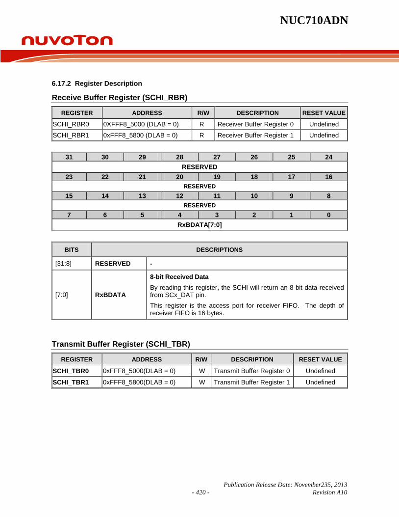
NUC710ADN
Publication Release Date: November235, 2013 - 420 - Revision A10
6.17.2 Register Description
Receive Buffer Register (SCHI_RBR)
REGISTER ADDRESS R/W DESCRIPTION RESET VALUE
SCHI_RBR0 0XFFF8_5000 (DLAB = 0) R Receiver Buffer Register 0 Undefined
SCHI_RBR1 0xFFF8_5800 (DLAB = 0) R Receiver Buffer Register 1 Undefined
31 30 29 28 27 26 25 24
RESERVED 23 22 21 20 19 18 17 16
RESERVED 15 14 13 12 11 10 9 8
RESERVED 7 6 5 4 3 2 1 0
RxBDATA[7:0]
BITS DESCRIPTIONS
[31:8] RESERVED -
[7:0] RxBDATA
8-bit Received Data By reading this register, the SCHI will return an 8-bit data received from SCx_DAT pin. This register is the access port for receiver FIFO. The depth of receiver FIFO is 16 bytes.
Transmit Buffer Register (SCHI_TBR)
REGISTER ADDRESS R/W DESCRIPTION RESET VALUE
SCHI_TBR0 0xFFF8_5000(DLAB = 0) W Transmit Buffer Register 0 Undefined
SCHI_TBR1 0xFFF8_5800(DLAB = 0) W Transmit Buffer Register 1 Undefined

NUC710ADN
Publication Release Date: November23, 2013 - 421 - Revision A10
BITS DESCRIPTIONS
[31:8] RESERVED -
[7:0] TxBDATA
8-bit Transmit Buffer Data By writing to this register, the SCHI will send 8-bit data through the SCx_DAT pin. This register is the access port for transmitter FIFO. The depth of transmitter FIFO is 16 bytes.
Interrupt Enable register (SCHI_IER)
REGISTER ADDRESS R/W DESCRIPTION RESET VALUE
SCHI_IER0 0xFFF8_5004 (DLAB = 0) R/W Interrupt Enable Register 0 0x0000_0080
SCHI_IER1 0xFFF8_5804 (DLAB = 0) R/W Interrupt Enable Register 1 0x0000_0080
31 30 29 28 27 26 25 24 RESERVED
23 22 21 20 19 18 17 16 RESERVED
15 14 13 12 11 10 9 8 RESERVED
7 6 5 4 3 2 1 0 TxBDATA[7:0]
31 30 29 28 27 26 25 24
RESERVED
23 22 21 20 19 18 17 16
RESERVED
15 14 13 12 11 10 9 8 RESERVED ETOR2 ETOR1 ETOR0
7 6 5 4 3 2 1 0 PWRDN Interface RESERVED ESCPTI ESCSRI ETBREI ERDRI

NUC710ADN
Publication Release Date: November235, 2013 - 422 - Revision A10
BITS DESCRIPTIONS
[31:11] RESERVED -
[10] ETOR2
TOR2 interrupt enable bit When 24-bit countdown timer reaches zero, it sets TO2 flag to high. If we set ETOR2 to high, then the 24-bit timer interrupts the CPU to indicate timeout.
[9] ETOR1
TOR1 interrupt enable bit When the 16-bit countdown timer reaches zero, it will set TO1 flag to high. If we set ETOR1 to high, then the 16-bit timer interrupts the CPU to indicate timeout.
[8] ETOR0
TOR0 interrupt enable bit When 8 bit countdown timer reaches zero, it will set the TO0 flag to high. If we set ETOR0 to high, then the 8-bit timer interrupts the CPU to indicate timeout.
[7] PWRDN
Smart card POWER DOWN bit PWRDN is used when the Smartcard controller needs to be powered down. Powering down must be done whenever the controller needs to switch between class A and B. When this bit is a 1, it will deactivate all contacts to the Smartcard except for SCRST_L, which is discussed later. When the Smartcard is removed, the H/W will also set the POWER DOWN bit.
[6] Interface
Smart card different interface bit Interface is used for controlling the different power control device signals. When set to 1, a power control pin is set to active high by the controller. When 0, the power control pin is active low to meet the needs of different power control interfaces.
[5:4] RESERVED Reserved for future
[3] ESCPTI
Smart card present toggle interrupt enable bit A rising/falling edge of SCPSNT signal triggers an interrupt if this bit is set to 1. 0 = SCPSNT toggle interrupt is disabled. 1 = SCPSNT toggle interrupt is enabled.
[2] ESCSRI
Enable SCSR interrupt bit An ESCSRI means interrupt enable bit for SCSR-related events such as silent byte detected error, no stop bit error, parity bit error or overrun error. Any SCSR-related event as described above will trigger an interrupt if this bit is set to 1. 0 = SCSR-related event interrupt is disabled. 1 = SCSR-related event interrupt is enabled.

NUC710ADN
Publication Release Date: November23, 2013 - 423 - Revision A10
Continued
BITS DESCRIPTIONS
[1] ETBREI
Enable Transmit Buffer Empty interrupt bit An ETBREI means interrupt enable bit for TBR (Transmitter Buffer Register) empty condition. An interrupt is issued when TBR is empty and this bit is set to 1. 0 = TBR empty interrupt is disabled. 1 = TBR empty interrupt is enabled.
[0] ERDRI
Enable Receive Data Ready interrupt bit The active FIFO threshold level for this kind of interrupt when FIFO is enabled is specified in RxTL1 and RxTL0 (bit 7 and bit 6 of the SCFR at base address+8, please refer to the SCFR description for more details). An interrupt is issued if a data byte is ready for host to read when FIFO is disabled or incoming data from the card reaches an active FIFO threshold level when FIFO is enabled.
Interrupt Status Register (SCHI_ISR)
REGISTER ADDRESS R/W DESCRIPTION RESET VALUE
SCHI_ISR0 0xFFF8_5008 (DLAB = 0) R Interrupt Status Register 0 0x0000_00C1
SCHI_ISR1 0xFFF8_5808 (DLAB = 0) R Interrupt Status Register 1 0x0000_00C1
This register contains mainly interrupt status including transmission-related interrupts and SCPSNT toggle interrupt. Transmission-related interrupt status is coded and prioritized as in UART implementation. The user may also find FIFO enable/disabled status reflecting what is set in bit 0 of the SCFR (write only Smart Card FIFO Register at base address + 8 when BDLAB = 0) and SCPSNT line status.
31 30 29 28 27 26 25 24
RESERVED
23 22 21 20 19 18 17 16
RESERVED
15 14 13 12 11 10 9 8 RESERVED
7 6 5 4 3 2 1 0
RESERVED SCPSNT SCPTI INTS2 INTS1 INTS0 Interrupt pending

NUC710ADN
Publication Release Date: November235, 2013 - 424 - Revision A10
BITS DESCRIPTIONS [31:6] RESERVED -
[5] SCPSNT
Smart card present line status. User may poll this bit to see the SCPSNT pin's voltage level 0 = Smart card is not connected to the reader 1 = Smart card IC is connected to the reader
[4] SCPTI
SCPSNT toggle interrupt status. A rising/falling edge of SCPSNT signal triggers an interrupt and set this status bit if ESCPTI (IER bit 3) is set to 1 to enable SCPSNT toggle interrupt. 0= No SCPSNT toggle interrupt. 1 = SCPSNT toggle interrupt occurs.
[3:1] INTS2 ~ INTS0
Interrupt Status bit 2 ~0 The combination indicates which kind of transmission-related interrupt has occurred. Refer to the following table for details.
ISR bit Interrupt set and function 3 2 1 0 Priority Interrupt
type Interrupt source Clear interrupt condition
0 0 0 1 - - No interrupt pending - 1 0 1 0 first Card
insert or remove
SCPTI =1 Read ISR
1 1 1 0 second TIME-OUT interrupt
1. TO2 =1 2. TO1 =1 3. TO0 =1
Read SCSR
0 1 1 0 third Data receiving status
1. OER = 1 2. PBER = 1 3. NSER = 1 4. SBD = 1
Read SCSR
0 1 0 0 fourth RBR data ready
1. RBR data ready 2. FIFO interrupt
active level reached
1. Read RBR 2. Read RBR until FIFO
is under active level 1 1 0 0 fifth FIFO
data time out
Receiver FIFO is non-empty and no activities are occurred in the receiver FIFO during the TOR defined time duration
Read RBR
0 0 1 0 sixth TBR empty
TBR empty 1. Write data to TBR 2. Read ISR (if priority
is sixth)
[0] Interrupt pending
Interrupt pending status bit. This bit is logical 1 if there is no interrupt pending. If an interrupt occurs, this bit is set to 0. 0 = Interrupt pending. 1 = No interrupt occurs.
Smart Card FIFO control Register (SCHI_SCFR)

NUC710ADN
Publication Release Date: November23, 2013 - 425 - Revision A10
REGISTER ADDRESS R/W DESCRIPTION RESET VALUE
SCHI_SCFR0 0xFFF8_5008 (DLAB = 0) W Interrupt Status Register 0 0x0000_0000
SCHI_SCFR1 0xFFF8_5808 (DLAB = 0) W Interrupt Status Register 1 0x0000_0000
BITS DESCRIPTIONS
[31:8] RESERVED -
[7:6] RxTL1, RxTL0
Receiver FIFO active Threshold Level control bits. These two bits are used to set the active level for the receiver FIFO interrupt. For example, if the interrupt active level is set as 4 bytes, once there are at least 4 data characters in the receiver FIFO, an interrupt is activated to notify host to read data from FIFO. Default to be 00b.
RxTL1 RxTL0 Rx FIFO Interrupt Active Level (Bytes) 0 0 01 0 1 04 1 0 08 1 1 14
31 30 29 28 27 26 25 24
RESERVED
23 22 21 20 19 18 17 16
RESERVED
15 14 13 12 11 10 9 8 RESERVED
7 6 5 4 3 2 1 0 RxTL1 RxTL0 PEC2 PEC1 PEC0 TxFRST RxFRST Reserved

NUC710ADN
Publication Release Date: November235, 2013 - 426 - Revision A10
Continued
BITS DESCRIPTIONS
[5:3] PEC2, PEC1, PEC0
Parity Error Count. Bits PEC2, PEC1 and PEC0 determine the number of allowed repetitions in reception or in transmission before setting bit PBER in SCSR. The value 000 indicates that, if only one parity error has occurred, bit PE is set; the value 111 indicate that bit PE is set after 8 parity errors. In protocol T =0: If a correct character is received before the programmed error number is reached, the error counter is reset If the programmed number of allowed parity errors is reached, the PBER bit in the register SCSR is set as long as the SCSR register has not been read. If a transmitted character is NAK by the card, then the smart card host interface automatically retransmits it a number of times equal to the value programmed in bits PEC2, PEC1 and PEC0 by generating an interrupt to inform the CPU to flush the transmit buffer. In transmission mode, if bits PEC2, PEC1 and PEC0 are logic 0, then the automatic retransmission is invalided. The retransmitted character starts after the guard time. So if you set the Guard Time register to 2 and the card pulls 2 ETU’s (elementary time unit) low, then there is no Guard Time. Set Guard Time =3 when T=0 in case 2 ETU’s are pulled down if NAK by the card. In protocol T= 1: The error counter has no action; bit PE is set at the first incorrectly received character.
[2] TxFRST Transmitter FIFO Reset control bit. Setting this bit to a logical 1 resets the transmitter FIFO counter to initial state. This bit is self-cleared to 0 after being set to 1. Default is 0.
[1] RxFRST Receiver FIFO Reset control bit. Setting this bit to a logical 1 resets the receiver FIFO counter to its initial state. This bit self-clears to 0 after being set to 1. Default is 0.
[0] RESERVED -
Smart Card Control Register (SCHI_SCCR)
REGISTER ADDRESS R/W DESCRIPTION RESET VALUE SCHI_SCCR0 0xFFF8_500C R/W Smart Card Control Register 0 0x0000_0018
SCHI_SCCR1 0xFFF8_580C R/W Smart Card Control Register 1 0x0000_0018
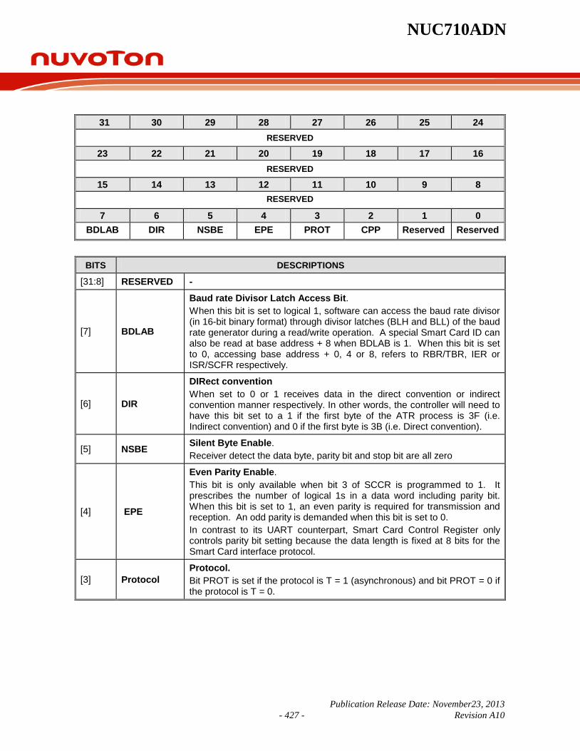
NUC710ADN
Publication Release Date: November23, 2013 - 427 - Revision A10
BITS DESCRIPTIONS
[31:8] RESERVED -
[7] BDLAB
Baud rate Divisor Latch Access Bit. When this bit is set to logical 1, software can access the baud rate divisor (in 16-bit binary format) through divisor latches (BLH and BLL) of the baud rate generator during a read/write operation. A special Smart Card ID can also be read at base address + 8 when BDLAB is 1. When this bit is set to 0, accessing base address + 0, 4 or 8, refers to RBR/TBR, IER or ISR/SCFR respectively.
[6] DIR
DIRect convention When set to 0 or 1 receives data in the direct convention or indirect convention manner respectively. In other words, the controller will need to have this bit set to a 1 if the first byte of the ATR process is 3F (i.e. Indirect convention) and 0 if the first byte is 3B (i.e. Direct convention).
[5] NSBE Silent Byte Enable. Receiver detect the data byte, parity bit and stop bit are all zero
[4] EPE
Even Parity Enable. This bit is only available when bit 3 of SCCR is programmed to 1. It prescribes the number of logical 1s in a data word including parity bit. When this bit is set to 1, an even parity is required for transmission and reception. An odd parity is demanded when this bit is set to 0. In contrast to its UART counterpart, Smart Card Control Register only controls parity bit setting because the data length is fixed at 8 bits for the Smart Card interface protocol.
[3] Protocol Protocol. Bit PROT is set if the protocol is T = 1 (asynchronous) and bit PROT = 0 if the protocol is T = 0.
31 30 29 28 27 26 25 24 RESERVED
23 22 21 20 19 18 17 16 RESERVED
15 14 13 12 11 10 9 8 RESERVED
7 6 5 4 3 2 1 0 BDLAB DIR NSBE EPE PROT CPP Reserved Reserved
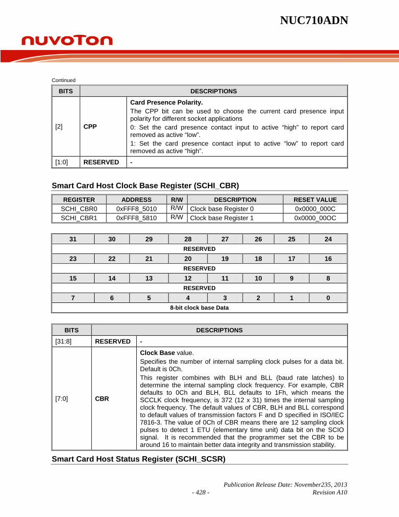
NUC710ADN
Publication Release Date: November235, 2013 - 428 - Revision A10
Continued
BITS DESCRIPTIONS
[2] CPP
Card Presence Polarity. The CPP bit can be used to choose the current card presence input polarity for different socket applications 0: Set the card presence contact input to active “high” to report card removed as active “low”. 1: Set the card presence contact input to active “low” to report card removed as active “high”.
[1:0] RESERVED -
Smart Card Host Clock Base Register (SCHI_CBR) REGISTER ADDRESS R/W DESCRIPTION RESET VALUE
SCHI_CBR0 0xFFF8_5010 R/W Clock base Register 0 0x0000_000C SCHI_CBR1 0xFFF8_5810 R/W Clock base Register 1 0x0000_00OC
BITS DESCRIPTIONS
[31:8] RESERVED -
[7:0] CBR
Clock Base value. Specifies the number of internal sampling clock pulses for a data bit. Default is 0Ch. This register combines with BLH and BLL (baud rate latches) to determine the internal sampling clock frequency. For example, CBR defaults to 0Ch and BLH, BLL defaults to 1Fh, which means the SCCLK clock frequency, is 372 (12 x 31) times the internal sampling clock frequency. The default values of CBR, BLH and BLL correspond to default values of transmission factors F and D specified in ISO/IEC 7816-3. The value of 0Ch of CBR means there are 12 sampling clock pulses to detect 1 ETU (elementary time unit) data bit on the SCIO signal. It is recommended that the programmer set the CBR to be around 16 to maintain better data integrity and transmission stability.
Smart Card Host Status Register (SCHI_SCSR)
31 30 29 28 27 26 25 24 RESERVED
23 22 21 20 19 18 17 16 RESERVED
15 14 13 12 11 10 9 8 RESERVED
7 6 5 4 3 2 1 0 8-bit clock base Data

NUC710ADN
Publication Release Date: November23, 2013 - 429 - Revision A10
REGISTER ADDRESS R/W DESCRIPTION RESET VALUE
SCHI_SCSR0 0xFFF8_5014 R Smart card Status Register 0 0x0000_0060
SCHI_SCSR1 0xFFF8_5814 R Smart card Status Register 1 0x0000_0060
BITS DESCRIPTIONS
[31:11] RESERVED RESERVED
[10:8] TOF2, TOF1, TOF0
TOF2 is the Timeout Flag of Timer2. When Timer 2 times out, it will set the FLAG (TOF2) When host reads SCSR, it clears this bit to 0. TOF1 is the Timeout Flag of Timer1. When Timer 1 times out, it will set the FLAG (TOF1) When host reads SCSR, it clears this bit to 0. TOF0 is the Timeout Flag of Timer0. When Timer 0 times out, it will set the FLAG (TOF0) When host reads SCSR, it clears this bit to 0.
[7] SC_RESET SC_RESET pin status This bit reflects if the RESET pin is high or low.
[6] TSRE Transmitter Shift Register Empty This bit is set to 1 when the transmitter shift register is empty.
[5] TBRE
Transmitter Buffer Register Empty In non-FIFO mode, this bit is set to a logical 1 when a data byte is transferred from TBR to TSR. If ETBREI of IER is a logical 1, an interrupt is generated to notify the host to write the following data bytes. In FIFO mode, this bit is set to 1 when the transmitter FIFO is empty. It is cleared to 0 when the host writes data bytes into TBR or FIFO.
31 30 29 28 27 26 25 24
RESERVED
23 22 21 20 19 18 17 16
RESERVED
15 14 13 12 11 10 9 8
RESERVED TOF2 TOF1 TOF0
7 6 5 4 3 2 1 0 SC_RESET TSRE TBRE SBD NSER PBER OER RDR

NUC710ADN
Publication Release Date: November235, 2013 - 430 - Revision A10
Continued
BITS DESCRIPTIONS
[4] SBD
Silent Byte Detected This bit is set to 1 to indicate the received data byte is kept in the silent state for a full byte time, including start bit, data bits, parity bit, and stop bits. In FIFO mode, it indicates the same condition for the data on top of FIFO. When the host reads SCSR, it clears this bit to 0.
[3] NSER
No Stop Bit Error This bit is set to 1 to indicate the received data has no stop bit. In FIFO mode, it indicates the same condition for the data on top of FIFO. When the host reads SCSR, it clears this bit to 0.
[2] PBER
Parity Bit Error This bit is set to 1 to indicate that the parity bit of the received data is wrong. In FIFO mode, it indicates the same condition for the data on top of the FIFO. When host reads SCSR, it clears this bit to 0.
[1] OER
Overrun Error This bit is set to 1 to indicate the previously received data is overwritten by the next received data before it is read by the host. In FIFO mode, it indicates the same condition instead of FIFO full. When the host reads SCSR, it clears this bit to 0.
[0] RDR
Receiver Data Ready This bit is set to 1 to indicate the received data is ready to be read by the host in RBR or FIFO. If no data are left in RBR or FIFO, the bit is cleared to 0.
Smart Card Host Guard Time Register (SCHI_GTR)
REGISTER ADDRESS R/W DESCRIPTION RESET VALUE
SCHI_GTR0 0xFFF8_5018 R/W Guard Time Register 0 0x0000_0001
SCHI_GTR1 0xFFF8_5818 R/W Guard Time Register 1 0x0000_0001
BITS DESCRIPTIONS
31 30 29 28 27 26 25 24 RESERVED
23 22 21 20 19 18 17 16 RESERVED
15 14 13 12 11 10 9 8 RESERVED
7 6 5 4 3 2 1 0 GTR [7:0]

NUC710ADN
Publication Release Date: November23, 2013 - 431 - Revision A10
[31:8] RESERVED -
[7:0] GTR
Guard Time Register value. This register specifies number of stop bits appended to the end of a data byte. Bit 7 ~ 0: Guard Time values. Default to be 01h.
Smart Card Host Extended Control Register (SCHI_ECR)
REGISTER ADDRESS R/W DESCRIPTION RESET VALUE SCHI_ECR0 0xFFF8_501C R/W Extended Control Register 0 0x0000_0052 SCHI_ECR1 0xFFF8_581C R/W Extended Control Register 1 0x0000_0052
BITS DESCRIPTIONS [31:11] RESERVED -
[10:8] PSCKFS2, PSCKFS1, PSCKFS0
PSCK Frequency Selection Bit 2, 1 and 0. This selection can adjust power-on /power-off sequence interval. They select working clock frequency as following table. Default values are 05h.
SCKFS0, SCKFS1, SCKFS2
SCCLK frequency
000 80MHz 001 40 MHz 010 20 MHz 011 10 MHz 100 5 MHz 101 2.5 MHz 110 1.25 MHz
31 30 29 28 27 26 25 24
RESERVED
23 22 21 20 19 18 17 16
RESERVED
15 14 13 12 11 10 9 8
RESERVED PSCKFS2 PSCKFS1 PSCKFS0
7 6 5 4 3 2 1 0
Reserved SCKFS2 SCKFS1 SCKFS0 CLKSTP CLKSTPL Reserved

NUC710ADN
Publication Release Date: November235, 2013 - 432 - Revision A10
Continued
BITS DESCRIPTIONS
[6:4] SCKFS2, SCKFS1, SCKFS0
SCCLK Frequency Selection Bit 2, 1 and 0. The working clock frequency selection is as follows. Default values are 05h.
SCKFS0, SCKFS1, SCKFS2
SCCLK frequency
000 80MHz 001 40 MHz 010 20 MHz 011 10 MHz 100 5 MHz 101 2.5 MHz 110 1.25 MHz
[3] CLKSTPL Clock Stop Voltage Level 0 = SCCLK stops at low if CLKSTP is also set to 0. 1 = SCCLK stops at high if CLKSTP is also set to 1.
[2] CLKSTP Clock Stop Control Bit Setting 1 to this bit stops SCCLK at a voltage level specified by CLKSTPL (bit 3 of ECR).
[1:0] RESERVED -
Smart Card Host Test Mode Register (SCHI_TMR)
REGISTER ADDRESS R/W DESCRIPTION RESET VALUE
SCHI_TMR0 0xFFF8_5020 R/W Test mode Register 0 0x0000_0000
SCHI_TMR1 0XFFF8_5820 R/W Test mode Register 1 0x0000_0000
This 8-bit register is added in order to allow better testing of the Smart Card host. Currently only bit 1 is used. In the future, other bits can be used to program the host and improve the testing platform.
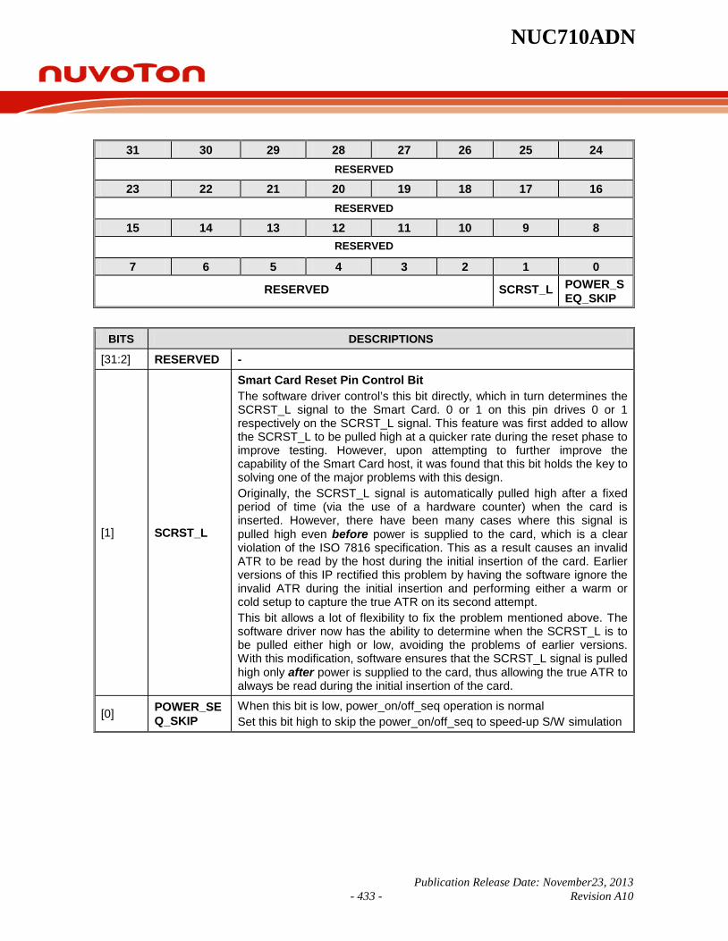
NUC710ADN
Publication Release Date: November23, 2013 - 433 - Revision A10
BITS DESCRIPTIONS
[31:2] RESERVED -
[1] SCRST_L
Smart Card Reset Pin Control Bit The software driver control’s this bit directly, which in turn determines the SCRST_L signal to the Smart Card. 0 or 1 on this pin drives 0 or 1 respectively on the SCRST_L signal. This feature was first added to allow the SCRST_L to be pulled high at a quicker rate during the reset phase to improve testing. However, upon attempting to further improve the capability of the Smart Card host, it was found that this bit holds the key to solving one of the major problems with this design. Originally, the SCRST_L signal is automatically pulled high after a fixed period of time (via the use of a hardware counter) when the card is inserted. However, there have been many cases where this signal is pulled high even before power is supplied to the card, which is a clear violation of the ISO 7816 specification. This as a result causes an invalid ATR to be read by the host during the initial insertion of the card. Earlier versions of this IP rectified this problem by having the software ignore the invalid ATR during the initial insertion and performing either a warm or cold setup to capture the true ATR on its second attempt. This bit allows a lot of flexibility to fix the problem mentioned above. The software driver now has the ability to determine when the SCRST_L is to be pulled either high or low, avoiding the problems of earlier versions. With this modification, software ensures that the SCRST_L signal is pulled high only after power is supplied to the card, thus allowing the true ATR to always be read during the initial insertion of the card.
[0] POWER_SEQ_SKIP
When this bit is low, power_on/off_seq operation is normal Set this bit high to skip the power_on/off_seq to speed-up S/W simulation
31 30 29 28 27 26 25 24 RESERVED
23 22 21 20 19 18 17 16 RESERVED
15 14 13 12 11 10 9 8 RESERVED
7 6 5 4 3 2 1 0
RESERVED SCRST_L POWER_SEQ_SKIP
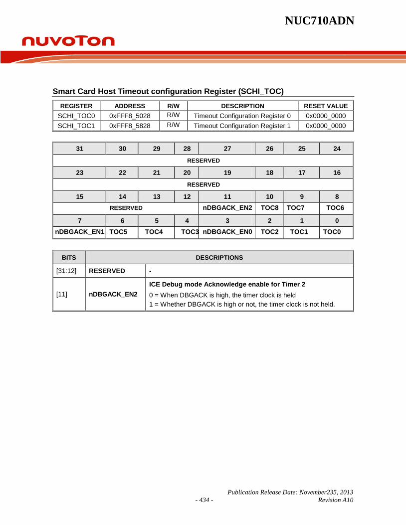
NUC710ADN
Publication Release Date: November235, 2013 - 434 - Revision A10
Smart Card Host Timeout configuration Register (SCHI_TOC)
REGISTER ADDRESS R/W DESCRIPTION RESET VALUE SCHI_TOC0 0xFFF8_5028 R/W Timeout Configuration Register 0 0x0000_0000 SCHI_TOC1 0xFFF8_5828 R/W Timeout Configuration Register 1 0x0000_0000
BITS DESCRIPTIONS
[31:12] RESERVED -
[11] nDBGACK_EN2 ICE Debug mode Acknowledge enable for Timer 2 0 = When DBGACK is high, the timer clock is held 1 = Whether DBGACK is high or not, the timer clock is not held.
31 30 29 28 27 26 25 24
RESERVED
23 22 21 20 19 18 17 16
RESERVED
15 14 13 12 11 10 9 8 RESERVED nDBGACK_EN2 TOC8 TOC7 TOC6
7 6 5 4 3 2 1 0 nDBGACK_EN1 TOC5 TOC4 TOC3 nDBGACK_EN0 TOC2 TOC1 TOC0
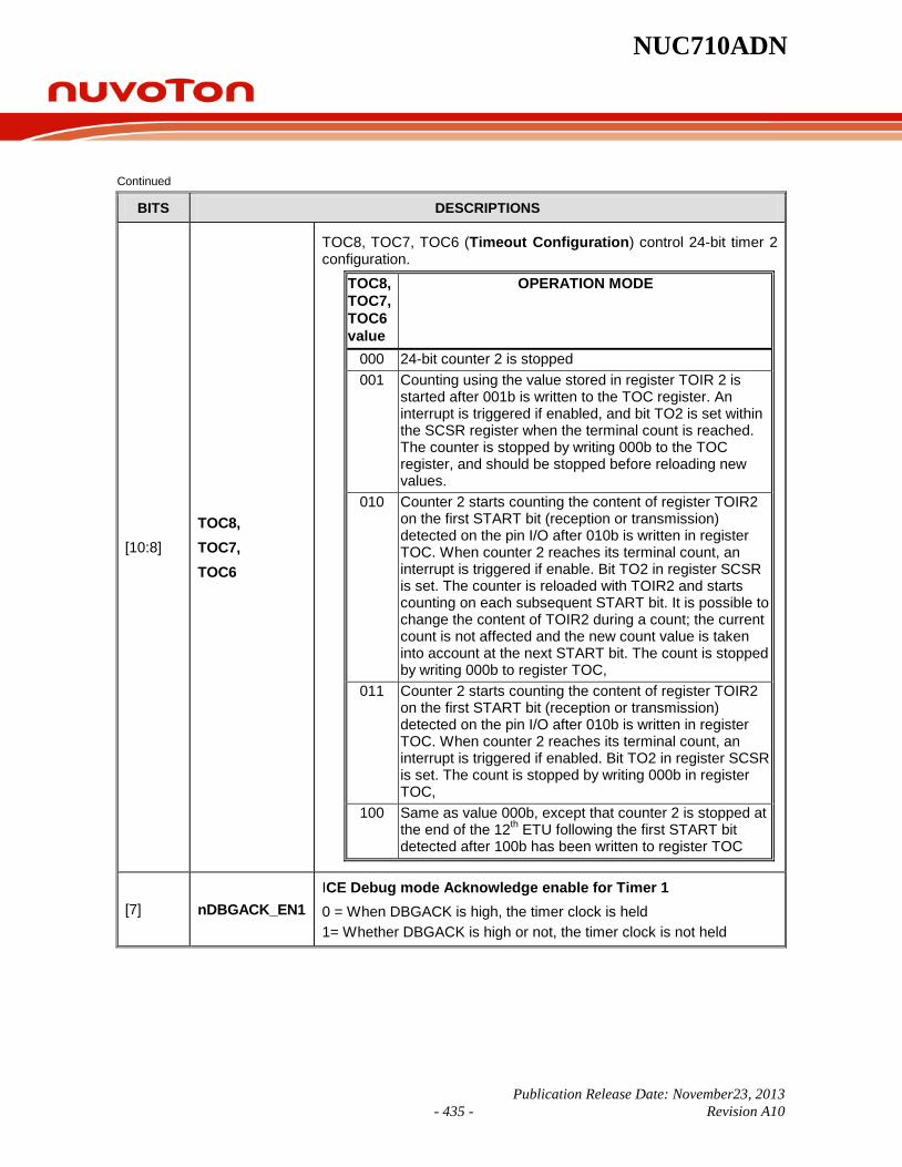
NUC710ADN
Publication Release Date: November23, 2013 - 435 - Revision A10
Continued
BITS DESCRIPTIONS
[10:8] TOC8, TOC7, TOC6
TOC8, TOC7, TOC6 (Timeout Configuration) control 24-bit timer 2 configuration.
TOC8, TOC7, TOC6 value
OPERATION MODE
000 24-bit counter 2 is stopped 001 Counting using the value stored in register TOIR 2 is
started after 001b is written to the TOC register. An interrupt is triggered if enabled, and bit TO2 is set within the SCSR register when the terminal count is reached. The counter is stopped by writing 000b to the TOC register, and should be stopped before reloading new values.
010 Counter 2 starts counting the content of register TOIR2 on the first START bit (reception or transmission) detected on the pin I/O after 010b is written in register TOC. When counter 2 reaches its terminal count, an interrupt is triggered if enable. Bit TO2 in register SCSR is set. The counter is reloaded with TOIR2 and starts counting on each subsequent START bit. It is possible to change the content of TOIR2 during a count; the current count is not affected and the new count value is taken into account at the next START bit. The count is stopped by writing 000b to register TOC,
011 Counter 2 starts counting the content of register TOIR2 on the first START bit (reception or transmission) detected on the pin I/O after 010b is written in register TOC. When counter 2 reaches its terminal count, an interrupt is triggered if enabled. Bit TO2 in register SCSR is set. The count is stopped by writing 000b in register TOC,
100 Same as value 000b, except that counter 2 is stopped at the end of the 12th ETU following the first START bit detected after 100b has been written to register TOC
[7] nDBGACK_EN1 ICE Debug mode Acknowledge enable for Timer 1 0 = When DBGACK is high, the timer clock is held 1= Whether DBGACK is high or not, the timer clock is not held

NUC710ADN
Publication Release Date: November235, 2013 - 436 - Revision A10
Continued
BITS DESCRIPTIONS
[6:4] TOC5, TOC4, TOC3
TOC5, TOC4, TOC3 (Timeout Configuration) control 16-bit timer 1 configuration. TOC5, TOC4, TOC3 value
OPERATION MODE
000 16-bit counter 1 is stopped 001 Counting the value stored in register TOIR 1 is started after
001b is written to register TOC. An interrupt is triggered if enabled, and bit TO1 is set within register SCSR when the terminal count is reached. The counter is stopped by writing 000b to register TOC, and should be stopped before reloading new values in register TOC.
010 Counter 1 starts counting the contents of register TOIR1 on the first START bit (reception or transmission) detected on the pin I/O after 010b is written to register TOC. When counter 1 reaches its terminal count, an interrupt is triggered if enabled. Bit TO1 in register SCSR is set. The counter is reloaded with TOIR1 and starts counting on each subsequent START bit. It is possible to change the content of TOIR1 during a count; the current count is not affected and the new count value is taken into account at the next START bit. The count is stopped by writing 000b to register TOC,
011 Counter 1 starts counting the content of register TOIR1 on the first START bit (reception or transmission) detected on the pin I/O after 010b is written to register TOC. When counter 1 reaches its terminal count, an interrupt is triggered if enabled. Bit TO1 in register SCSR is set. The count is stopped by writing 000b to register TOC,
100 Same as value 000b, except that counter 1 is stopped at the end of the 12th ETU following the first START bit detected after 100b has been written to register TOC
[3] nDBGACK_EN0 ICE Debug mode Acknowledge enabled for Timer 0 0 = When DBGACK is high, the timer clock is held 1 = Whether DBGACK is high or not, the timer clock is not held
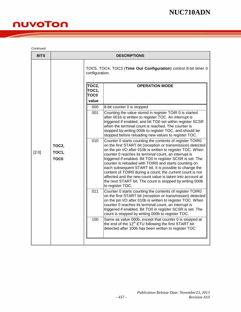
NUC710ADN
Publication Release Date: November23, 2013 - 437 - Revision A10
Continued
BITS DESCRIPTIONS
[2:0] TOC2, TOC1, TOC0
TOC5, TOC4, TOC3 (Time Out Configuration) control 8-bit timer 0 configuration. TOC2, TOC1, TOC0 value
OPERATION MODE
000 8-bit counter 0 is stopped 001 Counting the value stored in register TOIR 0 is started
after 001b is written to register TOC. An interrupt is triggered if enabled, and bit TO0 set within register SCSR when the terminal count is reached. The counter is stopped by writing 000b to register TOC, and should be stopped before reloading new values to register TOC.
010 Counter 0 starts counting the contents of register TOIR0 on the first START bit (reception or transmission) detected on the pin I/O after 010b is written to register TOC. When counter 0 reaches its terminal count, an interrupt is triggered if enabled. Bit TO0 in register SCSR is set. The counter is reloaded with TOIR0 and starts counting on each subsequent START bit. It is possible to change the content of TOIR0 during a count; the current count is not affected and the new count value is taken into account at the next START bit. The count is stopped by writing 000b to register TOC,
011 Counter 0 starts counting the contents of register TOIR0 on the first START bit (reception or transmission) detected on the pin I/O after 010b is written to register TOC. When counter 0 reaches its terminal count, an interrupt is triggered if enabled. Bit TO0 in register SCSR is set. The count is stopped by writing 000b to register TOC,
100 Same as value 000b, except that counter 0 is stopped at the end of the 12th ETU following the first START bit detected after 100b has been written to register TOC
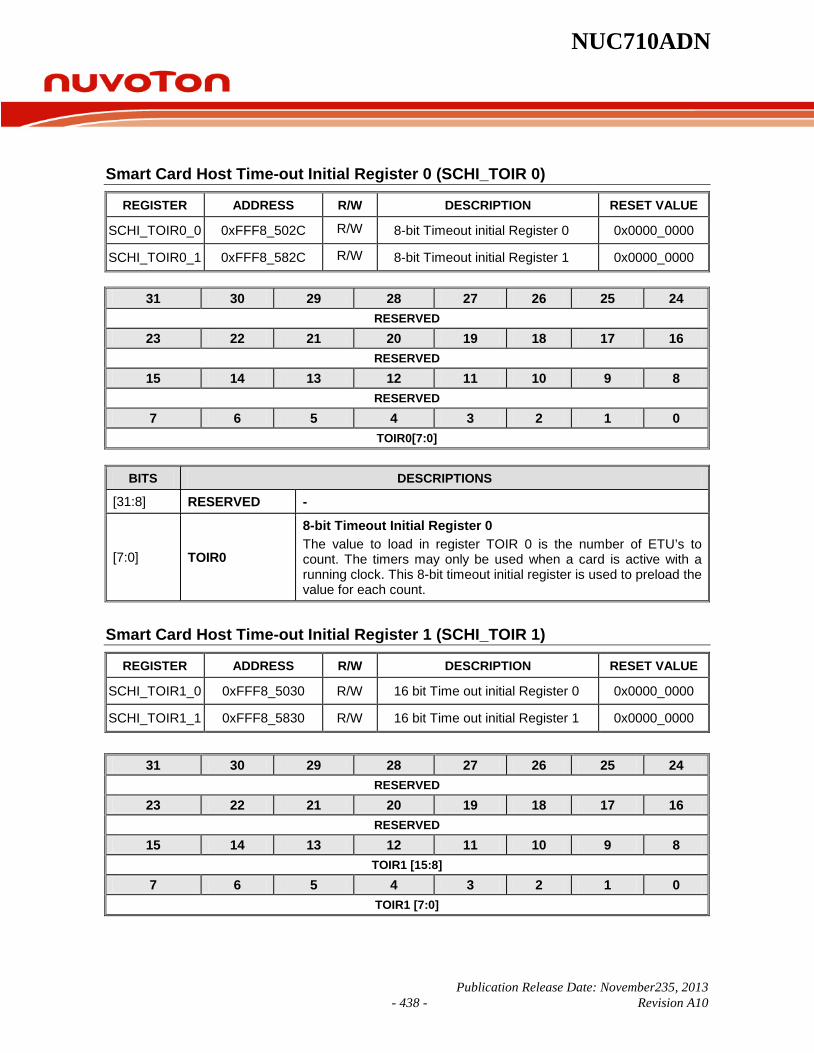
NUC710ADN
Publication Release Date: November235, 2013 - 438 - Revision A10
Smart Card Host Time-out Initial Register 0 (SCHI_TOIR 0)
REGISTER ADDRESS R/W DESCRIPTION RESET VALUE
SCHI_TOIR0_0 0xFFF8_502C R/W 8-bit Timeout initial Register 0 0x0000_0000
SCHI_TOIR0_1 0xFFF8_582C R/W 8-bit Timeout initial Register 1 0x0000_0000
BITS DESCRIPTIONS
[31:8] RESERVED -
[7:0] TOIR0
8-bit Timeout Initial Register 0 The value to load in register TOIR 0 is the number of ETU’s to count. The timers may only be used when a card is active with a running clock. This 8-bit timeout initial register is used to preload the value for each count.
Smart Card Host Time-out Initial Register 1 (SCHI_TOIR 1)
REGISTER ADDRESS R/W DESCRIPTION RESET VALUE
SCHI_TOIR1_0 0xFFF8_5030 R/W 16 bit Time out initial Register 0 0x0000_0000
SCHI_TOIR1_1 0xFFF8_5830 R/W 16 bit Time out initial Register 1 0x0000_0000
31 30 29 28 27 26 25 24 RESERVED
23 22 21 20 19 18 17 16 RESERVED
15 14 13 12 11 10 9 8 RESERVED
7 6 5 4 3 2 1 0 TOIR0[7:0]
31 30 29 28 27 26 25 24 RESERVED
23 22 21 20 19 18 17 16 RESERVED
15 14 13 12 11 10 9 8 TOIR1 [15:8]
7 6 5 4 3 2 1 0 TOIR1 [7:0]
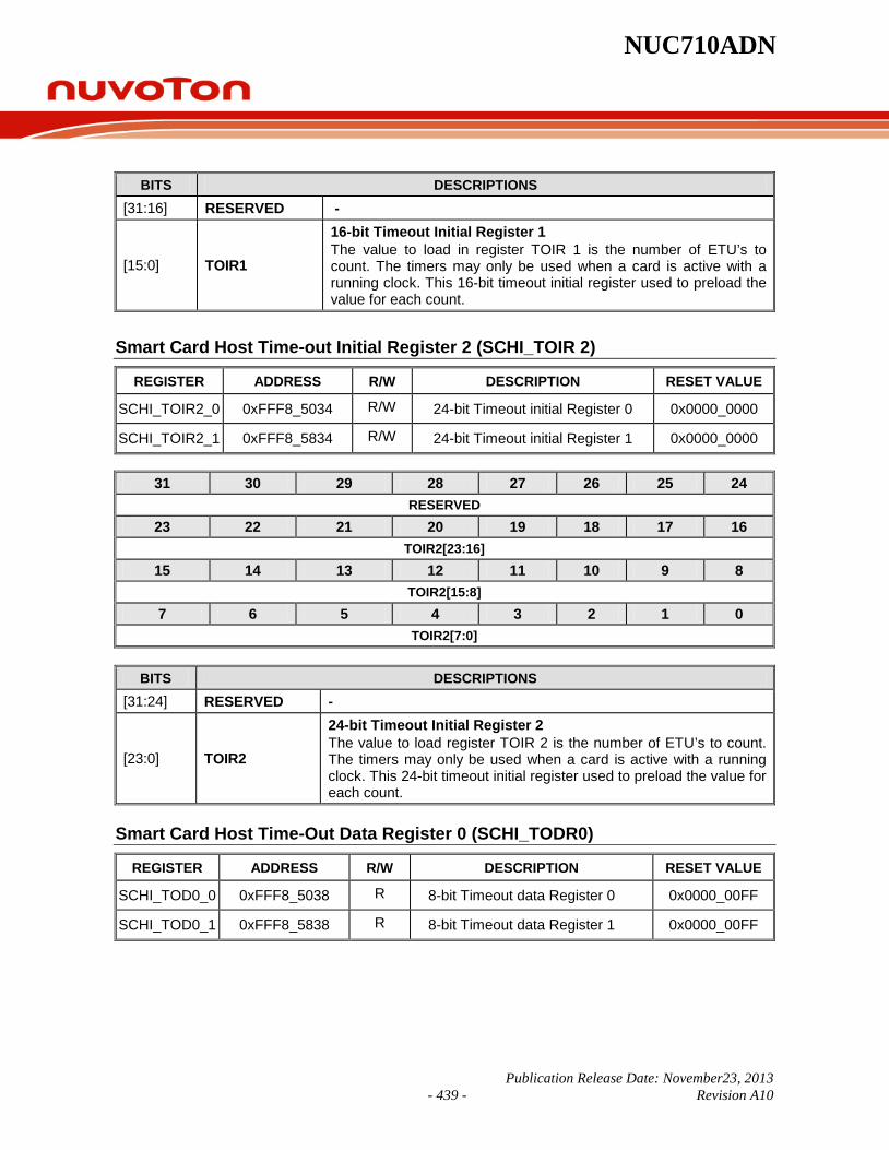
NUC710ADN
Publication Release Date: November23, 2013 - 439 - Revision A10
BITS DESCRIPTIONS [31:16] RESERVED -
[15:0] TOIR1
16-bit Timeout Initial Register 1 The value to load in register TOIR 1 is the number of ETU’s to count. The timers may only be used when a card is active with a running clock. This 16-bit timeout initial register used to preload the value for each count.
Smart Card Host Time-out Initial Register 2 (SCHI_TOIR 2)
REGISTER ADDRESS R/W DESCRIPTION RESET VALUE
SCHI_TOIR2_0 0xFFF8_5034 R/W 24-bit Timeout initial Register 0 0x0000_0000
SCHI_TOIR2_1 0xFFF8_5834 R/W 24-bit Timeout initial Register 1 0x0000_0000
BITS DESCRIPTIONS [31:24] RESERVED -
[23:0] TOIR2
24-bit Timeout Initial Register 2 The value to load register TOIR 2 is the number of ETU’s to count. The timers may only be used when a card is active with a running clock. This 24-bit timeout initial register used to preload the value for each count.
Smart Card Host Time-Out Data Register 0 (SCHI_TODR0)
REGISTER ADDRESS R/W DESCRIPTION RESET VALUE
SCHI_TOD0_0 0xFFF8_5038 R 8-bit Timeout data Register 0 0x0000_00FF
SCHI_TOD0_1 0xFFF8_5838 R 8-bit Timeout data Register 1 0x0000_00FF
31 30 29 28 27 26 25 24 RESERVED
23 22 21 20 19 18 17 16 TOIR2[23:16]
15 14 13 12 11 10 9 8 TOIR2[15:8]
7 6 5 4 3 2 1 0 TOIR2[7:0]
NUC710ADN
Publication Release Date: November235, 2013 - 440 - Revision A10
BITS DESCRIPTIONS
[31:8] RESERVED -
[7:0] TOD0
8 bit Timeout Data Count Register 0 The value shown in register TOD 0 is the number of ETU’s to count. The timeout data counters may only be used when a card is active with a running clock. This 8-bit timeout data register used to show the current counting value.
Smart Card Host Time-Out Data Register 1 (SCHI_TODR1)
REGISTER ADDRESS R/W DESCRIPTION RESET VALUE
SCHI_TOD1_0 0xFFF8_503C R 16 bit Timeout Data Register 0 0x0000_00FF
SCHI_TOD1_1 0xFFF8_583C R 16 bit Timeout Data Register 1 0x0000_00FF
BITS DESCRIPTIONS
[31:16] RESERVED -
[15:0] TOD1
16 bit Timeout Data Count Register 1 The value shown in register TOD 1 is the number of ETU’s to count. The timeout data counters may only be used when a card is active with a running clock. This 16-bit timeout data register used to show the current counting value.
Smart Card Host Time-Out Data Register 2 (SCHI_TODR2)
31 30 29 28 27 26 25 24 RESERVED
23 22 21 20 19 18 17 16 RESERVED
15 14 13 12 11 10 9 8 RESERVED
7 6 5 4 3 2 1 0 TOD0[7:0]
31 30 29 28 27 26 25 24 RESERVED
23 22 21 20 19 18 17 16 RESERVED
15 14 13 12 11 10 9 8 TOD1[15:8]
7 6 5 4 3 2 1 0 TDO1[7:0]

NUC710ADN
Publication Release Date: November23, 2013 - 441 - Revision A10
REGISTER ADDRESS R/W DESCRIPTION RESET VALUE
SCHI_TOD2_0 0xFFF8_5040 R 24 bit Timeout Data Register 0 0x0000_00FF
SCHI_TOD2_1 0xFFF8_5840 R 24 bit Timeout Data Register 1 0x0000_00FF
BITS DESCRIPTIONS
[31:24] RESERVED -
[23:0] TOR2
24 bit Timeout Data Count Register 2 The value to load in register TOD 2 is the number of ETU’s to count. The timers may only be used when a card is active with a running clock. This 24-bit timeout data register is used to show the current counting value.
Smart Card Host Buffer Timeout Data Register (SCHI_BTOR)
REGISTER ADDRESS R/W DESCRIPTION RESET VALUE
SCHI_BTOR0 0XFFF8_5044 R/W Buffer Timeout Data Register 0 0x0000_0000
SCHI_BTOR1 0XFFF8_5844 R/W Buffer Timeout Data Register 1 0x0000_0000
BITS DESCRIPTIONS
31 30 29 28 27 26 25 24 RESERVED
23 22 21 20 19 18 17 16 TOD2[23:16]
15 14 13 12 11 10 9 8 TOD2[15:8]
7 6 5 4 3 2 1 0 TDO2[7:0]
31 30 29 28 27 26 25 24 RESERVED
23 22 21 20 19 18 17 16 RESERVED
15 14 13 12 11 10 9 8 RESERVED
7 6 5 4 3 2 1 0 BTOIE BTOIC_6 BTOIC_5 BTOIC_4 BTOIC_3 BTOIC_2 BTOIC_1 BTOIC_0

NUC710ADN
Publication Release Date: November235, 2013 - 442 - Revision A10
[31:8] RESERVED -
[7] BTOIE Buffer Timeout Interrupt Enable The feature of receiver buffer timeout interrupt is enabled only when BTOIE[7] = ERDRI =1 .
[6:0] BTOIC
Buffer Timeout Interrupt Comparator The timeout counter resets and starts counting (the counter = ETU) whenever the RX FIFO receives a new data word. Once the content of the timeout counter (TOUT_CNT) is equal to that of time out interrupt comparator (TOIC), a receiver timeout interrupt (Irpt_TOUT) is generated if TOR[7] = ERDRI =1. A new incoming data word or BRX FIFO empty clear Irpt_TOUT.
Smart Card Host Baud Rate Divider Latch Lower Byte (SCHI_BLL)
REGISTER ADDRESS R/W DESCRIPTION RESET VALUE
SCHI_BLL0 0XFFF8_5000
(DLAB = 1) R/W Baud rate divisor Latch Lower byte Register 0 0x0000_001F
SCHI_BLL1 0XFFF8_5800
(DLAB = 1) R/W Baud rate divisor Latch Lower byte Register 1 0x0000_001F
BITS DESCRIPTIONS
[31:8] RESERVED -
[7:0] BLL
8 bit Baud Rate Divider Latch Low Byte Register This register combined with BLH and CBR determines the internal sampling clock frequency. Bit 7 ~ 0: Baud rate divisor latch lower byte values. Defaults to 1Fh.
Baud Rate Divider Latch Higher Byte (SCHI_BLH)
31 30 29 28 27 26 25 24 RESERVED
23 22 21 20 19 18 17 16 RESERVED
15 14 13 12 11 10 9 8 RESERVED
7 6 5 4 3 2 1 0 BLL[7:0]
NUC710ADN
Publication Release Date: November23, 2013 - 443 - Revision A10
REGISTER ADDRESS R/W DESCRIPTION RESET VALUE
SCHI_BLH0 0XFFF8_5004
(DLAB = 1) R/W Baud rate divisor Latch Higher byte Register 0 0x0000_0000
SCHI_BLH1 0XFFF8_5804
(DLAB = 1) R/W Baud rate divisor Latch Higher byte Register 1 0x0000_0000
BITS DESCRIPTIONS
[31:8] RESERVED -
[7:0] BLH
8 bit Baud rate divider Latch High byte register This register combined with BLL and CBR determines the internal sampling clock frequency. Bit 7 ~ 0: Baud rate divisor latch higher byte values. Default to be 00h.
SMART CARD ID NUMBER (SCHI_ID)
REGISTER ADDRESS R/W DESCRIPTION RESET VALUE
SCHI_ID0 0xFFF8_5008
(DLAB = 1) R Smart card ID number Register 0 0x0000_0070
SCHI_ID1 0XFFF8_5808
(DLAB = 1) R Smart card ID number Register 1 0x0000_0070
31 30 29 28 27 26 25 24 RESERVED
23 22 21 20 19 18 17 16 RESERVED
15 14 13 12 11 10 9 8 RESERVED
7 6 5 4 3 2 1 0 BLH[7:0]

NUC710ADN
Publication Release Date: November235, 2013 - 444 - Revision A10
BITS DESCRIPTIONS
[31:8] RESERVED -
[7:0] ID 8-bit smart card ID number register This register contains a specific value of 70h for the driver to identify the Smart Card interface.
31 30 29 28 27 26 25 24
RESERVED
23 22 21 20 19 18 17 16
RESERVED
15 14 13 12 11 10 9 8 RESERVED
7 6 5 4 3 2 1 0 ID[7:0]

NUC710ADN
Publication Release Date: November23, 2013 - 445 - Revision A10
6.17.3 Functional description The following description uses abbreviations to refer to control/status registers and their contents of the Smart Card interface as seen in section 6.17.2
Initialization User needs to program control registers so that ATR (Answer To Reset) data streams can be properly decoded after card insertion. Initialization settings include the following steps where sequential order is irrelevant. 1. BLH, BLL and CBR are written with 00h, 1Fh and 0Ch respectively to comply with default
transmission factors Fd and Dd, which are 372 and 1 as specified in ISO/IEC 7816-3. 2. GTR is programmed with 01h for one stop bit. 3. Set SCFR bit 1 to 1 to reset receiver FIFO. 4. Set EPE bit in SCCR bit 4 to be 1 for EVEN parity, set EPE bit to be 0 for odd parity. 5. Set SCKFS1 and SCKFS0 to "05" to select 2.5 MHz for SCCLK on 80MHz system clock. Most default values of above control bits are designed as specified in initialization step but it is recommended that the user perform the entire initialization sequence to avoid any ambiguity. The relationship between transmission factors and settings of BLH, BLL and CBR is best described in the following example.
f1
DFetu1 ×= (f means SCCLK frequency)
Therefore,
( ) 1231CBRBLL,BLH1
372DdFd
×=×==
Activation Card insertion pulls up SCn_PRES (assuming SCPSNT in ISR bit 5 is active high) and in consequence SCn_PWR is pulled down to activate power MOS to supply power to the card slot after a delay of about 5 ms. This delay is for the card slot mechanism to settle down before power is actually applied. SCn_CLK starts to output right after SCn_PWR is active while SCIO is in reception mode and pulled up externally. SCn_RST keeps low initially to reset the card but will output high after 512 clock cycles to meet requirement of tb of more than 400 clock cycles (specified in ISO/IEC 7816-3). To meet another timing requirement, tc of ISO/IEC 7816-3, a counter based on SCn_CLK is implemented to start counting on the rising edge of SCn_RST. SCn_PWR is deactivated if no ATR (Answer To Reset) is detected after 65536 clock cycles from the rising edge of SCn_RST.
Answer-to-Reset Answer-to-Reset (ATR) is the data streams sent by the card to the interface as an answer to a reset on SCn_RST signal. Refer to ISO/IEC 7816-3 for a detailed description of ATR. There are two kinds of cards specified in ISO/IEC 7816-3, inverse convention card and direct convention card. Although these two conventions treat logical meanings (0 or 1) of voltage levels (low or high) differently, Nuvoton's implementation of the Smart Card interface decodes a high voltage level data bit as 1 and low voltage level data bit as 0, and resorts to software to interpret incoming data. The software driver needs to interpret the initial ATR character first to determine which convention to use

NUC710ADN
Publication Release Date: November235, 2013 - 446 - Revision A10
for the inserted card and chooses a conversion procedure for it. Subsequent incoming data bytes must be passed through a conversion procedure before actually transferring these data bytes to the host. A similar conversion procedure must be applied to outgoing data bytes before writing to TBR as well. For example, the raw data byte for the initial character of inverse-convention ATR would be 3Fh. The software driver therefore needs a conversion procedure to reverse the bit-significance and polarity to process subsequent raw data bytes. On the other hand, the initial character of the direct-convention ATR is 3Bh, which needs no conversion procedure to process the data byte.
Data transfer Software driver might need to configure control registers again based on information contained in ATR before processing subsequent data transfers. The following guidelines are provided for programming reference. 1. EPE should be set to 1 for direct-convention card and otherwise for inverse-convention card. 2. BLH, BLL and CBR should be set to comply with Fi and Di. 3. GTR is used for various stop bit requirements of different transmission protocols. 4. Use the interrupt resources to control the communication sequence. 5. Monitor SCSR for transmission integrity.
Cold reset and warm reset Cold reset is achieved by writing a 1 to PWRDN (bit 7 of IER). It deactivates SCn_PWR to high. Consequentially, SCn_RST is pulled down and SCCLK is stopped. User must write a 0 to PWRDN (bit 7 of IER) to resume Smart Card interface to a normal activation state assuming card is still present. The activation sequence and deactivation sequence are done by internal F.S.M When in a normal activation state, writing a 0 SCRST_L (bit 1 of TMR) will force SCn_RST pin to low triggering a warm reset. Its effect is similar to a cold reset except that SCn_PWR is kept activated and therefore the power supply to the card stays on.
Power states SCHI employs a sophisticated algorithm to partition the Smart Card interface's internal circuits to achieve optimal power utilization. However, users must take extra care in the design of application circuits following guidelines stated below to prevent potential signal conflict and unnecessary power consumption. There are three power states: disabled state, active state, and power down state. The disabled state is the default state when power is first applied to the IC. SCPWD (Smart Card Power Down) controls whether in an active state (SCPWD = 0) or in the power down state (SCPWD = 1).
Disabled state Smart Card interface is initially disabled. The clock is idle in this state, and therefore this is the least power-consuming state. To prevent current leakage from floating connections, it is designed to output a predetermined voltage level on all the I/O pins of the Smart Card interface, as follows: SCn_PWR outputs high to disable power supply to socket; SCn_RST, SCn_CLK, and SCn_DAT output low; SCPSNT is tri-stated.

NUC710ADN
Publication Release Date: November23, 2013 - 447 - Revision A10
These I/O conditions also apply to sockets in the power down state (SCPWD = 1) or deselected socket in the idle state. Designers of application circuits must take extra care so that no contention occurs when Smart Card interface is in any power-saving state.
Active state Active state is when Smart Card interface is actually performing some function: configuring of control and interrupt registers, detecting card insertion/extraction, receiving ATR (Answer To Reset) information and communications packets from the host. Refer to section 7.12.3 for detailed function descriptions. This is the most power-consuming state, and actual power consumption is dependent on interface traffic.
Power down state Transition from an active state to the power down state is accomplished by setting SCPWD to 1. The clock is stopped for most internal core circuits except the detection circuit for SCPSNT toggle (card insertion/extraction). SCPSNT toggle can interrupt CPU and through this feature, the Smart Card interface in power down state can be woken up by card insertion/extraction. The programmer may also directly write a 0 to SCPWD to wake up the Smart Card interface. Smart Card interface spends a little bit more power to maintain SCPSNT toggle detection circuit in the power down state than in the disabled state which saves even more power than the active state by stopping clock for the core circuit. Programmers must ensure that all on-going transactions are concluded before putting the Smart Card interface into the power down state to prevent potential disoperation of the internal state machine.
NUC710ADN
Publication Release Date: November235, 2013 - 448 - Revision A10
6.18 I2C Interface I2C is a two-wire, bi-directional serial bus that provides a simple and efficient method of data exchange between devices. The I2C standard is a true multi-master bus including collision detection and arbitration that prevents data corruption if two or more masters attempt to control the bus simultaneously. Serial, 8-bit oriented bi-directional data transfers can be made up to 100 kbit/s in Standard-mode, up to 400 kbit/s in Fast-mode, or up to 3.4 Mbit/s in High-speed mode. Only 100kbps and 400kbps modes are supported directly. For High-speed mode special IOs are needed. If these IOs are available and used, then High-speed mode is also supported. Data is transferred between a Master and a Slave synchronously to SCL on the SDA line on a byte-by-byte basis. Each data byte is 8 bits long. There is one SCL clock pulse for each data bit with the MSB being transmitted first. An acknowledge bit follows each transferred byte. Each bit is sampled during the high period of SCL; and therefore, the SDA line may be changed only during the low period of SCL and must be held stable during the high period of SCL. A transition on the SDA line while SCL is high is interpreted as a command (START or STOP). The I2C Master Core includes the following features:
• AMBA APB interface compatible
• Compatible with Philips I2C standard, supports master mode
• Multi Master Operation
• Clock stretching and wait state generation
• Provide multi-byte transmit operation, up to 4 bytes can be transmitted in a single transfer
• Software programmable acknowledge bit
• Arbitration lost interrupt, with automatic transfer cancellation
• Start/Stop/Repeated Start/Acknowledge generation
• Start/Stop/Repeated Start detection
• Bus busy detection
• Supports 7 bit addressing mode
• Fully static synchronous design with one clock domain
• Software mode I2C

NUC710ADN
Publication Release Date: November23, 2013 - 449 - Revision A10
6.18.1 I2C Protocol Normally, a standard communication consists of four parts: 1) START or Repeated START signal generation
2) Slave address transfer
3) Data transfer
4) STOP signal generation
SCL
SDASorSr
MSB
ACK
PorSr
P
SrLSB MSB LSB
1 2 7 8 9 1 2 3 - 7 8 9
A6 A5 A4 - A1 A0 R/W D7 D6 D5 - D1 D0 NACKACK
Fig. 6.18.1.1 Data transfer on the I2C-bus
S SLAVE ADDRESS R/W A DATA A DATA A/A P
'0'(write)
data transfer(n bytes + acknowledge)
from master to slave
from slave to master
A = acknowledge (SDA low)A = not acknowledge (SDA high)S = START conditionP = STOP condition
A master-transmitter addressing a slave receiver with a 7-bit address
The transfer direction is not changed
'1'(read)
data transfer(n bytes + acknowledge)
S SLAVE ADDRESS R/W A DATA A DATA A P
A master reads a slave immediately after the first byte (address)
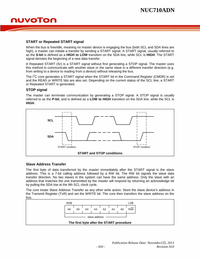
NUC710ADN
Publication Release Date: November235, 2013 - 450 - Revision A10
START or Repeated START signal When the bus is free/idle, meaning no master device is engaging the bus (both SCL and SDA lines are high), a master can initiate a transfer by sending a START signal. A START signal, usually referred to as the S-bit is defined as a HIGH to LOW transition on the SDA line, while SCL is HIGH. The START signal denotes the beginning of a new data transfer. A Repeated START (Sr) is a START signal without first generating a STOP signal. The master uses this method to communicate with another slave or the same slave in a different transfer direction (e.g. from writing to a device to reading from a device) without releasing the bus. The I2C core generates a START signal when the START bit in the Command Register (CMDR) is set and the READ or WRITE bits are also set. Depending on the current status of the SCL line, a START or Repeated START is generated.
STOP signal The master can terminate communication by generating a STOP signal. A STOP signal is usually referred to as the P-bit, and is defined as a LOW to HIGH transition on the SDA line, while the SCL is HIGH.
START condition STOP condition
SCL
SDA
START and STOP conditions
Slave Address Transfer The first byte of data transferred by the master immediately after the START signal is the slave address. This is a 7-bit calling address followed by a RW bit. The RW bit signals the slave data transfer direction. No two slaves in the system can have the same address. Only the slave with an address that matches the one transmitted by the master will respond by returning an acknowledge bit by pulling the SDA low at the 9th SCL clock cycle. The core treats Slave Address Transfer as any other write action. Store the slave device’s address in the Transmit Register (TxR) and set the WRITE bit. The core then transfers the slave address on the bus.
MSB LSB
R/WA0A1A2A3A4A5A6
slave address The first byte after the START procedure

NUC710ADN
Publication Release Date: November23, 2013 - 451 - Revision A10
Data Transfer Once slave addressing is complete, data transfer can proceed on a byte-by-byte basis in the direction specified by the RW bit sent by the master. Each transferred byte is followed by an acknowledge bit on the 9th SCL clock cycle. If the slave signals a Not Acknowledge (NACK), the master can generate a STOP signal to abort the data transfer or generate a Repeated START signal and start a new transfer cycle. If the master, as the receiving device, does Not Acknowledge (NACK) the slave, the slave releases the SDA line for the master to generate a STOP or Repeated START signal. To write data to a slave, store the data to be transmitted in the Transmit Register (TxR) and set the WRITE bit. To read data from a slave, set the READ bit. During a transfer the core set the I2C_TIP flag, indicating that a Transfer is In Progress. When the transfer is done the I2C_TIP flag is cleared, the IF flag is set if enabled, and then generates an interrupt. The Receive Register (RxR) contains valid data after the IF flag has been set. The software may issue a new write or read command when the I2C_TIP flag is cleared.
data linestable;
data valid
changeof dataallowed
SCL
SDA
Bit transfer on the I2C-bus
1 2 8 9SCL FROMMASTER
DATA OUTPUT BYTRANSMITTER
DATA OUTPUT BYRECEIVER S
STARTcondition
clock pulse foracknowledgement
not acknowledge
acknowledge
Acknowledge the I2C-bus
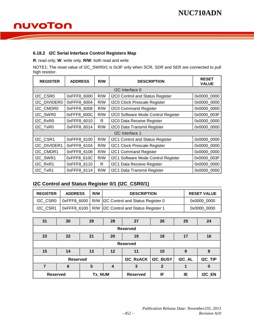
NUC710ADN
Publication Release Date: November235, 2013 - 452 - Revision A10
6.18.2 I2C Serial Interface Control Registers Map R: read only, W: write only, R/W: both read and write NOTE1: The reset value of I2C_SWR0/1 is 0x3F only when SCR, SDR and SER are connected to pull high resistor.
REGISTER ADDRESS R/W DESCRIPTION RESET VALUE
I2C Interface 0 I2C_CSR0 0xFFF8_6000 R/W I2C0 Control and Status Register 0x0000_0000 I2C_DIVIDER0 0xFFF8_6004 R/W I2C0 Clock Prescale Register 0x0000_0000 I2C_CMDR0 0xFFF8_6008 R/W I2C0 Command Register 0x0000_0000 I2C_SWR0 0xFFF8_600C R/W I2C0 Software Mode Control Register 0x0000_003F I2C_RxR0 0xFFF8_6010 R I2C0 Data Receive Register 0x0000_0000 I2C_TxR0 0xFFF8_6014 R/W I2C0 Data Transmit Register 0x0000_0000
I2C Interface 1 I2C_CSR1 0xFFF8_6100 R/W I2C1 Control and Status Register 0x0000_0000 I2C_DIVIDER1 0xFFF8_6104 R/W I2C1 Clock Prescale Register 0x0000_0000 I2C_CMDR1 0xFFF8_6108 R/W I2C1 Command Register 0x0000_0000 I2C_SWR1 0xFFF8_610C R/W I2C1 Software Mode Control Register 0x0000_003F I2C_RxR1 0xFFF8_6110 R I2C1 Data Receive Register 0x0000_0000 I2C_TxR1 0xFFF8_6114 R/W I2C1 Data Transmit Register 0x0000_0000
I2C Control and Status Register 0/1 (I2C_CSR0/1)
REGISTER ADDRESS R/W DESCRIPTION RESET VALUE
I2C_CSR0 0xFFF8_6000 R/W I2C Control and Status Register 0 0x0000_0000 I2C_CSR1 0xFFF8_6100 R/W I2C Control and Status Register 1 0x0000_0000
31 30 29 28 27 26 25 24
Reserved
23 22 21 20 19 18 17 16
Reserved
15 14 13 12 11 10 9 8
Reserved I2C_RxACK I2C_BUSY I2C_AL I2C_TIP 7 6 5 4 3 2 1 0
Reserved Tx_NUM Reserved IF IE I2C_EN

NUC710ADN
Publication Release Date: November23, 2013 - 453 - Revision A10
BITS DESCRIPTIONS
[31:12] Reserved Reserved
[11] I2C_RxACK
Received Acknowledge From Slave (Read only) This flag represents acknowledge from the addressed slave. 0 = Acknowledge received (ACK). 1 = Not acknowledge received (NACK).
[10] I2C_BUSY I2C Bus Busy (Read only) 0 = After STOP signal detected. 1 = After START signal detected.
[9] I2C_AL
Arbitration Lost (Read only) This bit is set when the I2C core lost arbitration. Arbitration is lost when: A STOP signal is detected, but not requested. The master drives SDA high, but SDA is low.
[8] I2C_TIP
Transfer In Progress (Read only) 0 = Transfer complete. 1 = Transferring data. NOTE: When a transfer is in progress, no writing to any I2C register of the master core except for SWR is allowed.
[5:4] Tx_NUM
Transmit Byte Counts These two bits represent how many bytes remain to transmit. When a byte has been transmitted, Tx_NUM would be subtracted by 1 until all bytes are transmitted (Tx_NUM = 0x0) or NACK received from slave. Then the interrupt signal will assert if IE was set. 0x0 = Only one byte is left for transmission. 0x1 = Two bytes are left for transmission. 0x2 = Three bytes are left for transmission. 0x3 = Four bytes are left for transmission.
[3] Reserved Reserved
[2] IF
Interrupt Flag The Interrupt Flag is set when: Transfer is complete. Transfer is not yet complete, but slave responded NACK (in multi-byte transmit mode). Arbitration is lost. NOTE: This bit is read only, but can be cleared by writing 1 to this bit.
[1] IE Interrupt Enable 0 = Disable I2C Interrupt. 1 = Enable I2C Interrupt.
[0] I2C_EN I2C Core Enable 0 = Disable I2C core, serial bus outputs are controlled by SDW/SCW. 1 = Enable I2C core, serial bus outputs are controlled by the I2C core.
I2C Prescale Register 0/1 (I2C_DIVIDER 0 /1)
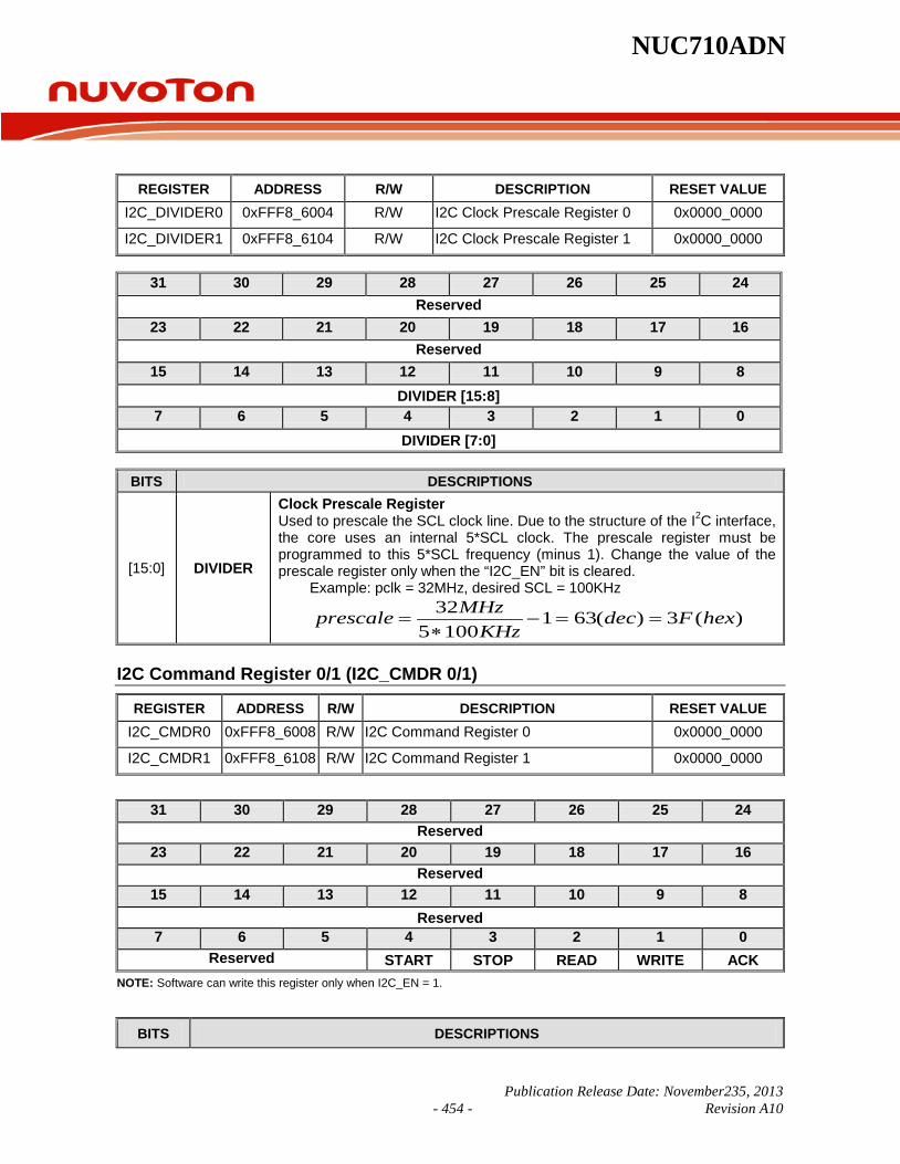
NUC710ADN
Publication Release Date: November235, 2013 - 454 - Revision A10
REGISTER ADDRESS R/W DESCRIPTION RESET VALUE I2C_DIVIDER0 0xFFF8_6004 R/W I2C Clock Prescale Register 0 0x0000_0000 I2C_DIVIDER1 0xFFF8_6104 R/W I2C Clock Prescale Register 1 0x0000_0000
31 30 29 28 27 26 25 24 Reserved
23 22 21 20 19 18 17 16 Reserved
15 14 13 12 11 10 9 8 DIVIDER [15:8]
7 6 5 4 3 2 1 0 DIVIDER [7:0]
BITS DESCRIPTIONS
[15:0] DIVIDER
Clock Prescale Register Used to prescale the SCL clock line. Due to the structure of the I2C interface, the core uses an internal 5*SCL clock. The prescale register must be programmed to this 5*SCL frequency (minus 1). Change the value of the prescale register only when the “I2C_EN” bit is cleared.
Example: pclk = 32MHz, desired SCL = 100KHz
)(3)(6311005
32 hexFdecKHz
MHzprescale ==−∗
=
I2C Command Register 0/1 (I2C_CMDR 0/1)
REGISTER ADDRESS R/W DESCRIPTION RESET VALUE I2C_CMDR0 0xFFF8_6008 R/W I2C Command Register 0 0x0000_0000 I2C_CMDR1 0xFFF8_6108 R/W I2C Command Register 1 0x0000_0000
31 30 29 28 27 26 25 24
Reserved 23 22 21 20 19 18 17 16
Reserved 15 14 13 12 11 10 9 8
Reserved 7 6 5 4 3 2 1 0
Reserved START STOP READ WRITE ACK NOTE: Software can write this register only when I2C_EN = 1.
BITS DESCRIPTIONS
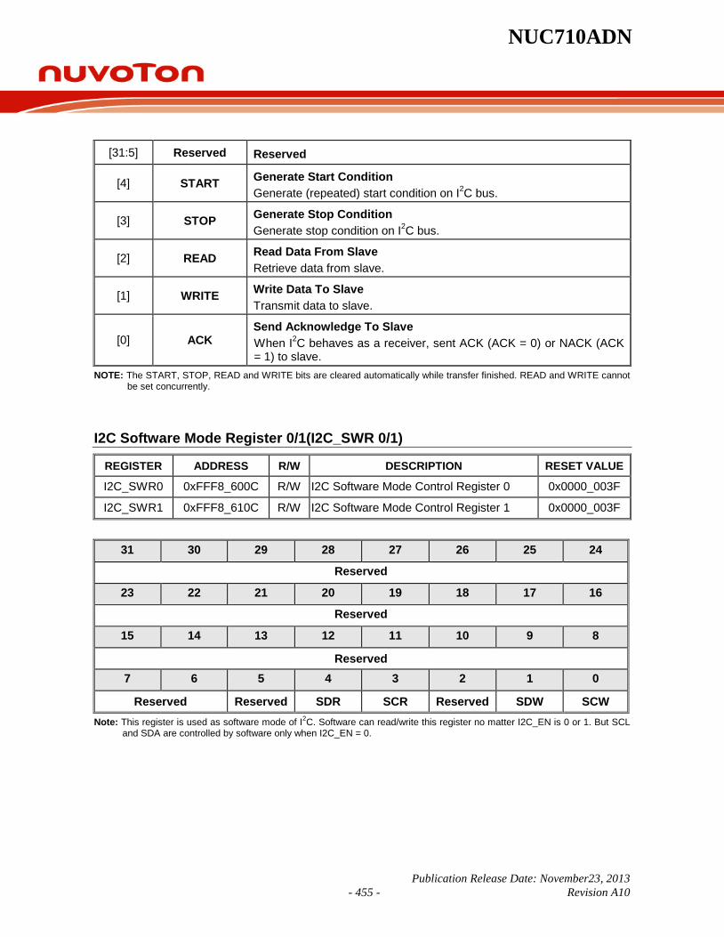
NUC710ADN
Publication Release Date: November23, 2013 - 455 - Revision A10
[31:5] Reserved Reserved
[4] START Generate Start Condition Generate (repeated) start condition on I2C bus.
[3] STOP Generate Stop Condition Generate stop condition on I2C bus.
[2] READ Read Data From Slave Retrieve data from slave.
[1] WRITE Write Data To Slave Transmit data to slave.
[0] ACK Send Acknowledge To Slave When I2C behaves as a receiver, sent ACK (ACK = 0) or NACK (ACK = 1) to slave.
NOTE: The START, STOP, READ and WRITE bits are cleared automatically while transfer finished. READ and WRITE cannot be set concurrently.
I2C Software Mode Register 0/1(I2C_SWR 0/1)
REGISTER ADDRESS R/W DESCRIPTION RESET VALUE
I2C_SWR0 0xFFF8_600C R/W I2C Software Mode Control Register 0 0x0000_003F I2C_SWR1 0xFFF8_610C R/W I2C Software Mode Control Register 1 0x0000_003F
31 30 29 28 27 26 25 24
Reserved
23 22 21 20 19 18 17 16
Reserved
15 14 13 12 11 10 9 8
Reserved 7 6 5 4 3 2 1 0
Reserved Reserved SDR SCR Reserved SDW SCW Note: This register is used as software mode of I2C. Software can read/write this register no matter I2C_EN is 0 or 1. But SCL
and SDA are controlled by software only when I2C_EN = 0.
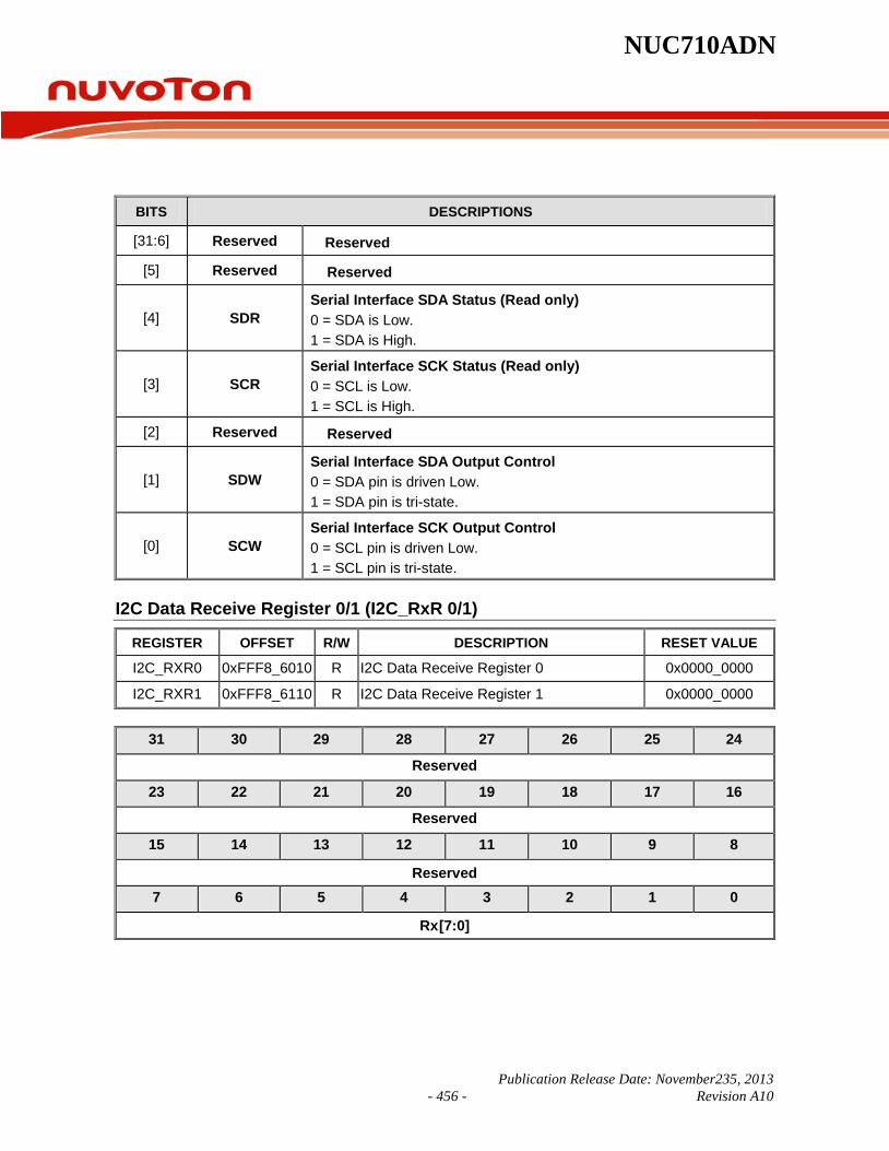
NUC710ADN
Publication Release Date: November235, 2013 - 456 - Revision A10
BITS DESCRIPTIONS
[31:6] Reserved Reserved
[5] Reserved Reserved
[4] SDR Serial Interface SDA Status (Read only) 0 = SDA is Low. 1 = SDA is High.
[3] SCR Serial Interface SCK Status (Read only) 0 = SCL is Low. 1 = SCL is High.
[2] Reserved Reserved
[1] SDW Serial Interface SDA Output Control 0 = SDA pin is driven Low. 1 = SDA pin is tri-state.
[0] SCW Serial Interface SCK Output Control 0 = SCL pin is driven Low. 1 = SCL pin is tri-state.
I2C Data Receive Register 0/1 (I2C_RxR 0/1)
REGISTER OFFSET R/W DESCRIPTION RESET VALUE
I2C_RXR0 0xFFF8_6010 R I2C Data Receive Register 0 0x0000_0000 I2C_RXR1 0xFFF8_6110 R I2C Data Receive Register 1 0x0000_0000
31 30 29 28 27 26 25 24
Reserved
23 22 21 20 19 18 17 16
Reserved
15 14 13 12 11 10 9 8
Reserved 7 6 5 4 3 2 1 0
Rx [7:0]
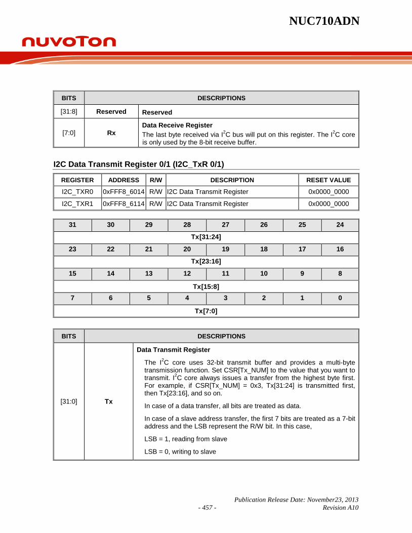
NUC710ADN
Publication Release Date: November23, 2013 - 457 - Revision A10
BITS DESCRIPTIONS
[31:8] Reserved Reserved
[7:0] Rx Data Receive Register The last byte received via I2C bus will put on this register. The I2C core is only used by the 8-bit receive buffer.
I2C Data Transmit Register 0/1 (I2C_TxR 0/1)
REGISTER ADDRESS R/W DESCRIPTION RESET VALUE
I2C_TXR0 0xFFF8_6014 R/W I2C Data Transmit Register 0x0000_0000 I2C_TXR1 0xFFF8_6114 R/W I2C Data Transmit Register 0x0000_0000
31 30 29 28 27 26 25 24
Tx [31:24]
23 22 21 20 19 18 17 16
Tx [23:16]
15 14 13 12 11 10 9 8
Tx [15:8] 7 6 5 4 3 2 1 0
Tx [7:0]
BITS DESCRIPTIONS
[31:0] Tx
Data Transmit Register
The I2C core uses 32-bit transmit buffer and provides a multi-byte transmission function. Set CSR[Tx_NUM] to the value that you want to transmit. I2C core always issues a transfer from the highest byte first. For example, if CSR[Tx_NUM] = 0x3, Tx[31:24] is transmitted first, then Tx[23:16], and so on.
In case of a data transfer, all bits are treated as data.
In case of a slave address transfer, the first 7 bits are treated as a 7-bit address and the LSB represent the R/W bit. In this case,
LSB = 1, reading from slave
LSB = 0, writing to slave
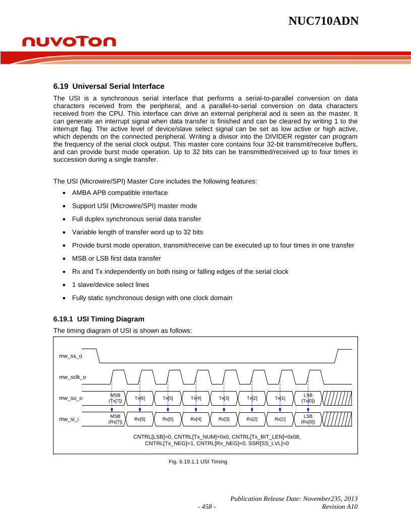
NUC710ADN
Publication Release Date: November235, 2013 - 458 - Revision A10
6.19 Universal Serial Interface The USI is a synchronous serial interface that performs a serial-to-parallel conversion on data characters received from the peripheral, and a parallel-to-serial conversion on data characters received from the CPU. This interface can drive an external peripheral and is seen as the master. It can generate an interrupt signal when data transfer is finished and can be cleared by writing 1 to the interrupt flag. The active level of device/slave select signal can be set as low active or high active, which depends on the connected peripheral. Writing a divisor into the DIVIDER register can program the frequency of the serial clock output. This master core contains four 32-bit transmit/receive buffers, and can provide burst mode operation. Up to 32 bits can be transmitted/received up to four times in succession during a single transfer. The USI (Microwire/SPI) Master Core includes the following features:
• AMBA APB compatible interface
• Support USI (Microwire/SPI) master mode
• Full duplex synchronous serial data transfer
• Variable length of transfer word up to 32 bits
• Provide burst mode operation, transmit/receive can be executed up to four times in one transfer
• MSB or LSB first data transfer
• Rx and Tx independently on both rising or falling edges of the serial clock
• 1 slave/device select lines
• Fully static synchronous design with one clock domain 6.19.1 USI Timing Diagram The timing diagram of USI is shown as follows:
MSB(Tx[7])
LSB(Tx[0])
MSB(Rx[7])
LSB(Rx[0])
mw_ss_o
mw_sclk_o
mw_so_o
mw_si_i
CNTRL[LSB]=0, CNTRL[Tx_NUM]=0x0, CNTRL[Tx_BIT_LEN]=0x08,CNTRL[Tx_NEG]=1, CNTRL[Rx_NEG]=0, SSR[SS_LVL]=0
Tx[6] Tx[5] Tx[4] Tx[3] Tx[2] Tx[1]
Rx[6] Rx[5] Rx[4] Rx[3] Rx[2] Rx[1]
Fig. 6.19.1.1 USI Timing

NUC710ADN
Publication Release Date: November23, 2013 - 459 - Revision A10
mw_ss_o
mw_sclk_o
mw_so_o
mw_si_i
CNTRL[LSB]=1, CNTRL[Tx_NUM]=0x0, CNTRL[Tx_BIT_LEN]=0x08,CNTRL[Tx_NEG]=0, CNTRL[Rx_NEG]=1, SSR[SS_LVL]=0
MSB(Tx[7])
LSB(Tx[0])
MSB(Rx[7])
LSB(Rx[0])
Tx[1] Tx[2] Tx[3] Tx[4] Tx[5] Tx[6]
Rx[1] Rx[2] Rx[3] Rx[4] Rx[5] Rx[6]
Fig. 6.19.1.2 Alternate Phase SCLK Clock Timing
6.19.2 USI Registers Map R: read only, W: write only, R/W: both read and write
REGISTER ADDRESS R/W DESCRIPTION RESET VALUE
USI_CNTRL 0xFFF8_6200 R/W Control and Status Register 0x0000_0004
USI_DIVIDER 0xFFF8_6204 R/W Clock Divider Register 0x0000_0000
USI_SSR 0xFFF8_6208 R/W Slave Select Register 0x0000_0000
Reserved 0xFFF8_620C N/A Reserved N/A
USI_Rx0 0xFFF8_6210 R Data Receive Register 0 0x0000_0000
USI_Rx1 0xFFF8_6214 R Data Receive Register 1 0x0000_0000
USI_Rx2 0xFFF8_6218 R Data Receive Register 2 0x0000_0000
USI_Rx3 0xFFF8_621C R Data Receive Register 3 0x0000_0000
USI_Tx0 0xFFF8_6210 W Data Transmit Register 0 0x0000_0000
USI_Tx1 0xFFF8_6214 W Data Transmit Register 1 0x0000_0000
USI_Tx2 0xFFF8_6218 W Data Transmit Register 2 0x0000_0000
USI_Tx3 0xFFF8_621C W Data Transmit Register 3 0x0000_0000
NOTE 1: When the software programs CNTRL, the GO_BUSY bit should be written last.
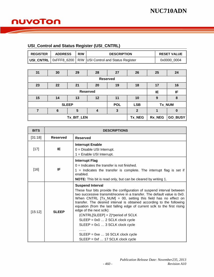
NUC710ADN
Publication Release Date: November235, 2013 - 460 - Revision A10
USI_Control and Status Register (USI_CNTRL)
REGISTER ADDRESS R/W DESCRIPTION RESET VALUE
USI_CNTRL 0xFFF8_6200 R/W USI Control and Status Register 0x0000_0004
31 30 29 28 27 26 25 24
Reserved
23 22 21 20 19 18 17 16
Reserved IE IF 15 14 13 12 11 10 9 8
SLEEP POL LSB Tx_NUM 7 6 5 4 3 2 1 0
Tx_BIT_LEN Tx_NEG Rx_NEG GO_BUSY
BITS DESCRIPTIONS
[31:18] Reserved Reserved
[17] IE Interrupt Enable 0 = Disable USI Interrupt. 1 = Enable USI Interrupt.
[16] IF
Interrupt Flag 0 = Indicates the transfer is not finished. 1 = Indicates the transfer is complete. The interrupt flag is set if enabled. NOTE: This bit is read only, but can be cleared by writing 1.
[15:12] SLEEP
Suspend Interval These four bits provide the configuration of suspend interval between two successive transmit/receive in a transfer. The default value is 0x0. When CNTRL [Tx_NUM] = 00, setting this field has no effect on transfer. The desired interval is obtained according to the following equation (from the last falling edge of current sclk to the first rising edge of the next sclk):
(CNTRL[SLEEP] + 2)*period of SCLK SLEEP = 0x0 … 2 SCLK clock cycle SLEEP = 0x1 … 3 SCLK clock cycle …… SLEEP = 0xe … 16 SCLK clock cycle SLEEP = 0xf … 17 SCLK clock cycle

NUC710ADN
Publication Release Date: November23, 2013 - 461 - Revision A10
Continued
BITS DESCRIPTIONS
[11] POL
Polarity This bit decides SCLK pin status when USI in idle state or transmission is completed. 1 = SCLK stops at high 0 = SCLK stops at low
[10] LSB
Send LSB First 0 = The MSB is transmitted/received first (which bit in the TxX/RxX register depends on the Tx_BIT_LEN field in the CNTRL register). 1 = The LSB is sent first on the line (bit TxX[0]), and the first bit received from the line is put in the LSB position in the Rx register (bit RxX[0]).
[9:8] Tx_NUM
Transmit/Receive Numbers This field specifies how many transmit/receive numbers should be executed in one transfer. 00 = Only one transmit/receive is executed in one transfer. 01 = Two successive transmits/receives are executed in one transfer. 10 = Three successive transmits/receives are executed in one transfer. 11 = Four successive transmits/receives are executed in one transfer.
[7:3] Tx_BIT_LEN
Transmit Bit Length This field specifies how many bits are transmitted in one transmit/receive. Up to 32 bits can be transmitted.
Tx_BIT_LEN = 0x01 … 1 bit Tx_BIT_LEN = 0x02 … 2 bits …… Tx_BIT_LEN = 0x1f … 31 bits Tx_BIT_LEN = 0x00 … 32 bits
[2] Tx_NEG Transmit On Negative Edge 0 = The mw_so_o signal is changed on the rising edge of mw_sclk_o. 1 = The mw_so_o signal is changed on the falling edge of mw_sclk_o.
[1] Rx_NEG Receive On Negative Edge 0 = The mw_si_i signal is latched on the rising edge of mw_sclk_o. 1 = The mw_si_i signal is latched on the falling edge of mw_sclk_o.
[0] GO_BUSY
Go and Busy Status 0 = Writing 0 to this bit has no effect. 1 = Writing 1 to this bit starts the transfer. This bit remains set during the transfer and is automatically cleared after the transfer finished. NOTE: All the registers should be set before writing 1 to the GO_BUSY bit in the CNTRL register. When a transfer is in progress, writing to any register of the USI(Microwire/SPI) master core has no effect.
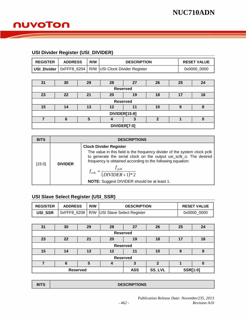
NUC710ADN
Publication Release Date: November235, 2013 - 462 - Revision A10
USI Divider Register (USI_DIVIDER)
REGISTER ADDRESS R/W DESCRIPTION RESET VALUE
USI_Divider 0xFFF8_6204 R/W USI Clock Divider Register 0x0000_0000
31 30 29 28 27 26 25 24 Reserved
23 22 21 20 19 18 17 16 Reserved
15 14 13 12 11 10 9 8 DIVIDER[15:8]
7 6 5 4 3 2 1 0 DIVIDER[7:0]
BITS DESCRIPTIONS
[15:0] DIVIDER
Clock Divider Register The value in this field is the frequency divider of the system clock pclk to generate the serial clock on the output usi_sclk_o. The desired frequency is obtained according to the following equation:
( ) 2*1+=
DIVIDERf
f pclksclk
NOTE: Suggest DIVIDER should be at least 1.
USI Slave Select Register (USI_SSR)
REGISTER ADDRESS R/W DESCRIPTION RESET VALUE USI_SSR 0xFFF8_6208 R/W USI Slave Select Register 0x0000_0000
31 30 29 28 27 26 25 24
Reserved 23 22 21 20 19 18 17 16
Reserved 15 14 13 12 11 10 9 8
Reserved 7 6 5 4 3 2 1 0
Reserved ASS SS_LVL SSR[1:0]
BITS DESCRIPTIONS
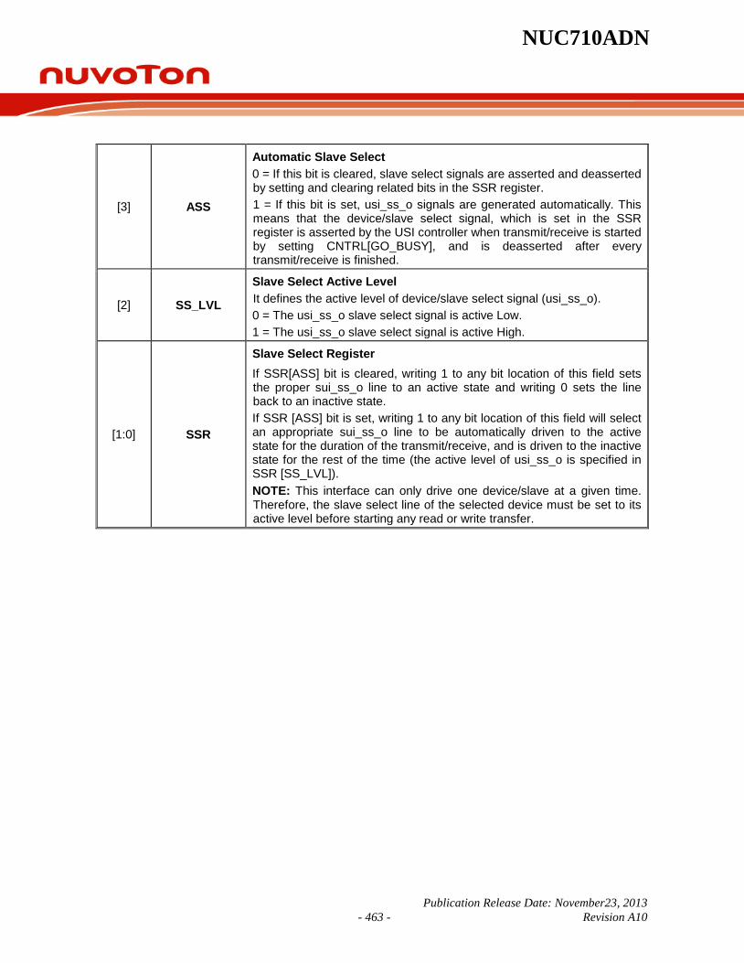
NUC710ADN
Publication Release Date: November23, 2013 - 463 - Revision A10
[3] ASS
Automatic Slave Select 0 = If this bit is cleared, slave select signals are asserted and deasserted by setting and clearing related bits in the SSR register. 1 = If this bit is set, usi_ss_o signals are generated automatically. This means that the device/slave select signal, which is set in the SSR register is asserted by the USI controller when transmit/receive is started by setting CNTRL[GO_BUSY], and is deasserted after every transmit/receive is finished.
[2] SS_LVL
Slave Select Active Level It defines the active level of device/slave select signal (usi_ss_o). 0 = The usi_ss_o slave select signal is active Low. 1 = The usi_ss_o slave select signal is active High.
[1:0] SSR
Slave Select Register If SSR[ASS] bit is cleared, writing 1 to any bit location of this field sets the proper sui_ss_o line to an active state and writing 0 sets the line back to an inactive state. If SSR [ASS] bit is set, writing 1 to any bit location of this field will select an appropriate sui_ss_o line to be automatically driven to the active state for the duration of the transmit/receive, and is driven to the inactive state for the rest of the time (the active level of usi_ss_o is specified in SSR [SS_LVL]). NOTE: This interface can only drive one device/slave at a given time. Therefore, the slave select line of the selected device must be set to its active level before starting any read or write transfer.
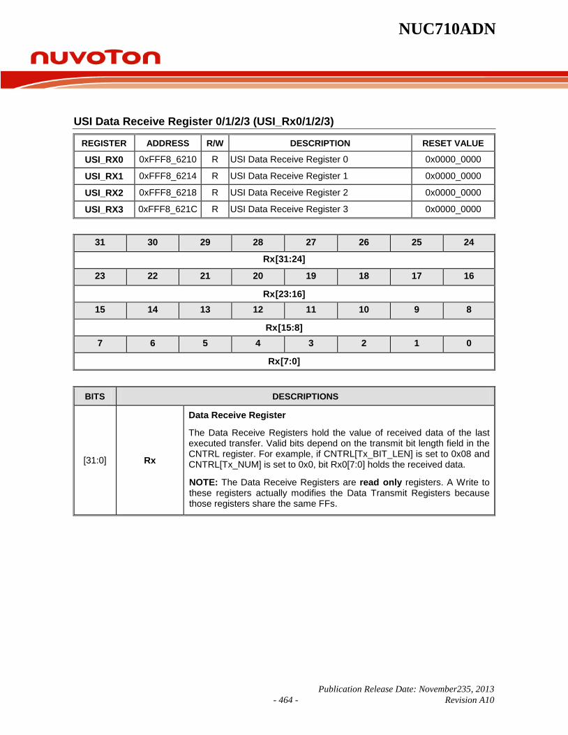
NUC710ADN
Publication Release Date: November235, 2013 - 464 - Revision A10
USI Data Receive Register 0/1/2/3 (USI_Rx0/1/2/3)
REGISTER ADDRESS R/W DESCRIPTION RESET VALUE
USI_RX0 0xFFF8_6210 R USI Data Receive Register 0 0x0000_0000 USI_RX1 0xFFF8_6214 R USI Data Receive Register 1 0x0000_0000 USI_RX2 0xFFF8_6218 R USI Data Receive Register 2 0x0000_0000 USI_RX3 0xFFF8_621C R USI Data Receive Register 3 0x0000_0000
31 30 29 28 27 26 25 24
Rx [31:24]
23 22 21 20 19 18 17 16
Rx [23:16] 15 14 13 12 11 10 9 8
Rx [15:8] 7 6 5 4 3 2 1 0
Rx [7:0]
BITS DESCRIPTIONS
[31:0] Rx
Data Receive Register
The Data Receive Registers hold the value of received data of the last executed transfer. Valid bits depend on the transmit bit length field in the CNTRL register. For example, if CNTRL[Tx_BIT_LEN] is set to 0x08 and CNTRL[Tx_NUM] is set to 0x0, bit Rx0[7:0] holds the received data.
NOTE: The Data Receive Registers are read only registers. A Write to these registers actually modifies the Data Transmit Registers because those registers share the same FFs.

NUC710ADN
Publication Release Date: November23, 2013 - 465 - Revision A10
Data Transmit Register 0/1/2/3 (Tx0/1/2/3)
REGISTER ADDRESS R/W DESCRIPTION RESET VALUE
USI_TX0 0xFFF8_6210 W USI Data Transmit Register 0 0x0000_0000 USI_TX1 0xFFF8_6214 W USI Data Transmit Register 1 0x0000_0000 USI_TX2 0xFFF8_6218 W USI Data Transmit Register 2 0x0000_0000 USI_TX3 0xFFF8_621C W USI Data Transmit Register 3 0x0000_0000
31 30 29 28 27 26 25 24
Tx [31:24]
23 22 21 20 19 18 17 16
Tx [23:16] 15 14 13 12 11 10 9 8
Tx [15:8] 7 6 5 4 3 2 1 0
Tx [7:0]
BITS DESCRIPTIONS
[31:0] Tx
Data Transmit Register
The Data Transmit Registers hold data to be transmitted in the next transfer. Valid bits depend on the transmit bit length field in the CNTRL register. For example, if CNTRL[Tx_BIT_LEN] is set to 0x08 and the CNTRL[Tx_NUM] is set to 0x0, the bit Tx0[7:0] is transmitted in next transfer. If CNTRL[Tx_BIT_LEN] is set to 0x00 and CNTRL[Tx_NUM] is set to 0x3, the core will perform four successive 32-bit transmits/receives using the same setting (the order is Tx0[31:0], Tx1[31:0], Tx2[31:0], Tx3[31:0]).
NOTE: The RxX and TxX registers share the same flip-flops, which means that what is received from the input data line in one transfer is transmitted on the output data line in the next transfer if no write access to the TxX register is executed between transfers.

NUC710ADN
Publication Release Date: November235, 2013 - 466 - Revision A10
6.20 PWM NUC710 has 4-channel PWM timers. They can be divided into two groups. Each group has 1 prescaler, 1 clock divider, 2 clock selectors, 2 16-bit counters, 2 16-bit comparators, 1 Dead-Zone generator. They are all driven by PCLK (80 MHz). Each channel can be used as a timer and issue interrupts independently. Two-channel PWM timers in one group share the same prescaler. Clock divider provides each channel with 5 clock sources (1, 1/2, 1/4, 1/8, 1/16). Each channel receives its own clock signal from the clock divider, which receives the clock signal from the 8-bit prescaler. The 16-bit counter of each channel receives clock signal from the clock selector and can be used to handle one PWM period. The 16-bit comparator compares number in the counter with the threshold number in register loaded previously to generate PWM duty cycle. The clock signal from the clock divider is called the PWM clock. The Dead-Zone generator uses the PWM clock as a clock source. Once the Dead-Zone generator is enabled, the output of the two PWM timers in one group is blocked. The two output pins are all used as Dead-Zone generator output signals to control off-chip powered devices. To prevent PWM driving the output pin with an unsteady waveform, 16-bit counter and 16-bit comparators are implemented with double buffering feature. The user is free to write data to the counter buffer register and comparator buffer register without problem. When the 16-bit down counter reaches zero, PWM Timer would generate interrupt request to inform the CPU that time is up. When the counter reaches zero, if the counter is set as toggle mode, it is automatically reloaded and starts to generate the next cycle. The user can set the counter as one-shot mode instead of toggle mode. If the counter is set as one-shot mode, the counter stops and generates one interrupt request when it reaches zero. The value of comparator is used for pulse width modulation. The counter control logic changes the output level when down-counter value matches the value of the compare register.
The PWM timer features are shown as below:
Two 8-bit prescalers and two clock dividers Four clock selectors Four 16-bit counters and four 16-bit comparators Two Dead-Zone generators
6.20.1 PWM double buffering and automatic reload NUC710 PWM Timers have a double buffering function, enabling the reload value to be changed for the next timer operation without stopping the current timer. Although the new timer value is set, current timer operation still operates successfully.
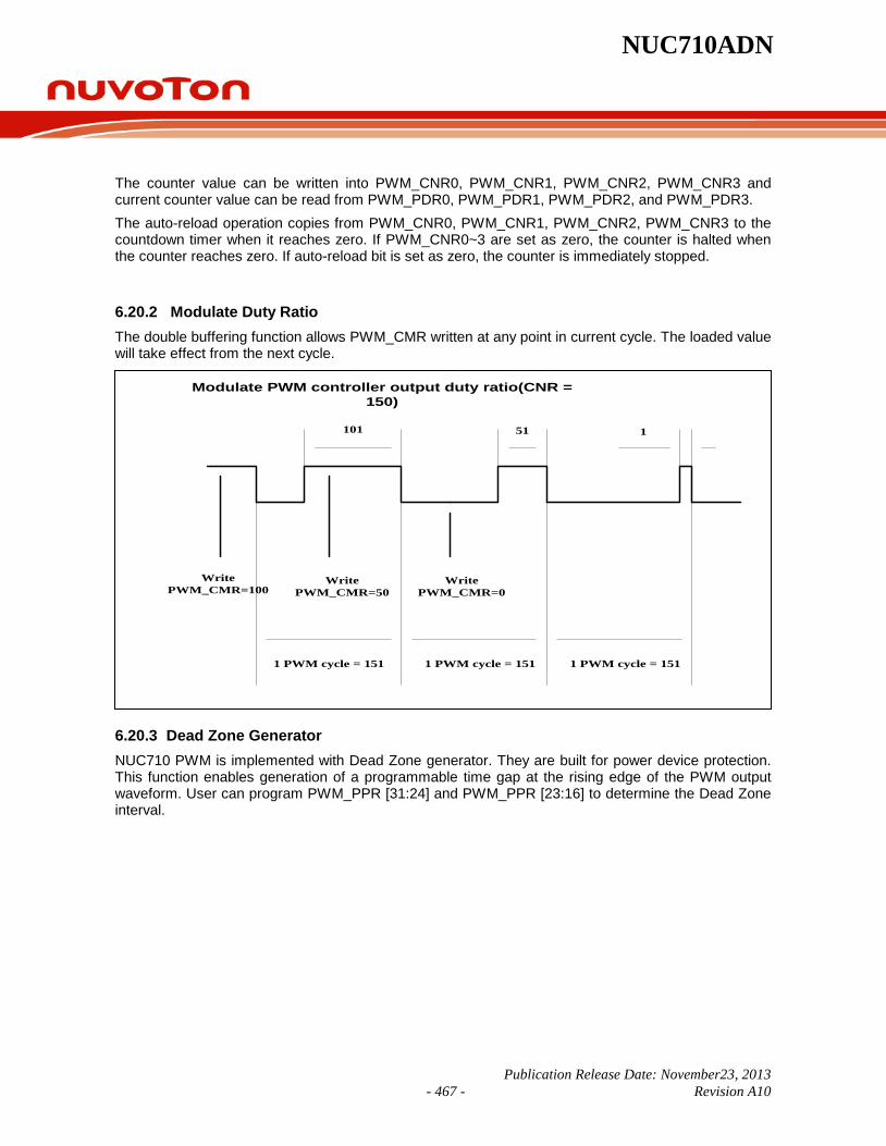
NUC710ADN
Publication Release Date: November23, 2013 - 467 - Revision A10
The counter value can be written into PWM_CNR0, PWM_CNR1, PWM_CNR2, PWM_CNR3 and current counter value can be read from PWM_PDR0, PWM_PDR1, PWM_PDR2, and PWM_PDR3. The auto-reload operation copies from PWM_CNR0, PWM_CNR1, PWM_CNR2, PWM_CNR3 to the countdown timer when it reaches zero. If PWM_CNR0~3 are set as zero, the counter is halted when the counter reaches zero. If auto-reload bit is set as zero, the counter is immediately stopped.
6.20.2 Modulate Duty Ratio The double buffering function allows PWM_CMR written at any point in current cycle. The loaded value will take effect from the next cycle.
Modulate PWM controller output duty ratio(CNR = 150)
Write PWM_CMR=100
Write PWM_CMR=50
Write PWM_CMR=0
1 PWM cycle = 151 1 PWM cycle = 151 1 PWM cycle = 151
101 51 1
6.20.3 Dead Zone Generator NUC710 PWM is implemented with Dead Zone generator. They are built for power device protection. This function enables generation of a programmable time gap at the rising edge of the PWM output waveform. User can program PWM_PPR [31:24] and PWM_PPR [23:16] to determine the Dead Zone interval.
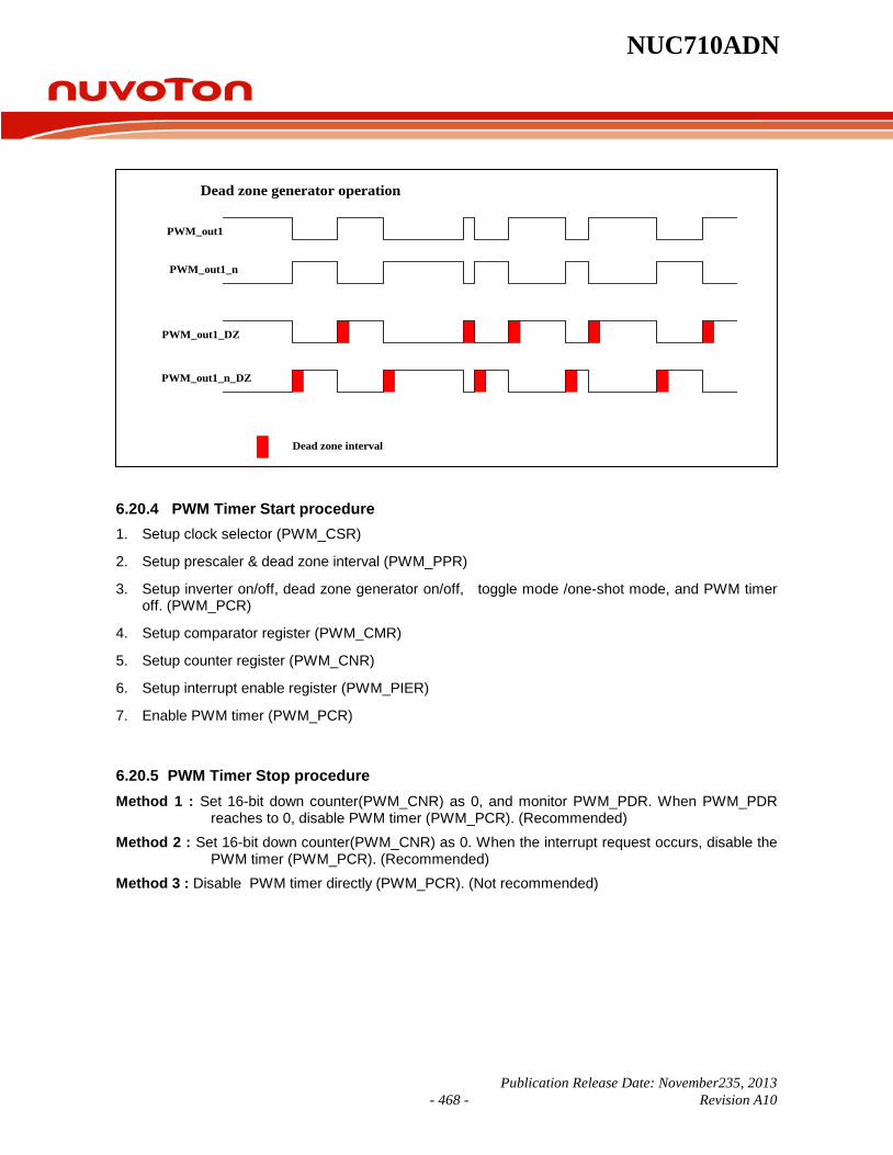
NUC710ADN
Publication Release Date: November235, 2013 - 468 - Revision A10
Dead zone generator operation
PWM_out1
PWM_out1_n
PWM_out1_DZ
PWM_out1_n_DZ
Dead zone interval
6.20.4 PWM Timer Start procedure 1. Setup clock selector (PWM_CSR)
2. Setup prescaler & dead zone interval (PWM_PPR)
3. Setup inverter on/off, dead zone generator on/off, toggle mode /one-shot mode, and PWM timer off. (PWM_PCR)
4. Setup comparator register (PWM_CMR)
5. Setup counter register (PWM_CNR)
6. Setup interrupt enable register (PWM_PIER)
7. Enable PWM timer (PWM_PCR)
6.20.5 PWM Timer Stop procedure Method 1 : Set 16-bit down counter(PWM_CNR) as 0, and monitor PWM_PDR. When PWM_PDR
reaches to 0, disable PWM timer (PWM_PCR). (Recommended) Method 2 : Set 16-bit down counter(PWM_CNR) as 0. When the interrupt request occurs, disable the
PWM timer (PWM_PCR). (Recommended) Method 3 : Disable PWM timer directly (PWM_PCR). (Not recommended)
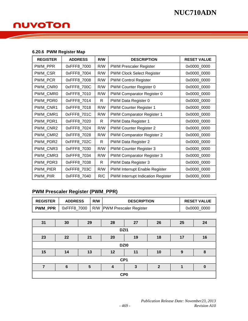
NUC710ADN
Publication Release Date: November23, 2013 - 469 - Revision A10
6.20.6 PWM Register Map
REGISTER ADDRESS R/W DESCRIPTION RESET VALUE
PWM_PPR 0xFFF8_7000 R/W PWM Prescaler Register 0x0000_0000
PWM_CSR 0xFFF8_7004 R/W PWM Clock Select Register 0x0000_0000
PWM_PCR 0xFFF8_7008 R/W PWM Control Register 0x0000_0000
PWM_CNR0 0xFFF8_700C R/W PWM Counter Register 0 0x0000_0000
PWM_CMR0 0xFFF8_7010 R/W PWM Comparator Register 0 0x0000_0000
PWM_PDR0 0xFFF8_7014 R PWM Data Register 0 0x0000_0000
PWM_CNR1 0xFFF8_7018 R/W PWM Counter Register 1 0x0000_0000
PWM_CMR1 0xFFF8_701C R/W PWM Comparator Register 1 0x0000_0000
PWM_PDR1 0xFFF8_7020 R PWM Data Register 1 0x0000_0000
PWM_CNR2 0xFFF8_7024 R/W PWM Counter Register 2 0x0000_0000
PWM_CMR2 0xFFF8_7028 R/W PWM Comparator Register 2 0x0000_0000
PWM_PDR2 0xFFF8_702C R PWM Data Register 2 0x0000_0000
PWM_CNR3 0xFFF8_7030 R/W PWM Counter Register 3 0x0000_0000
PWM_CMR3 0xFFF8_7034 R/W PWM Comparator Register 3 0x0000_0000
PWM_PDR3 0xFFF8_7038 R PWM Data Register 3 0x0000_0000
PWM_PIER 0xFFF8_703C R/W PWM Interrupt Enable Register 0x0000_0000
PWM_PIIR 0xFFF8_7040 R/C PWM Interrupt Indication Register 0x0000_0000
PWM Prescaler Register (PWM_PPR)
REGISTER ADDRESS R/W DESCRIPTION RESET VALUE
PWM_PPR 0xFFF8_7000 R/W PWM Prescaler Register 0x0000_0000
31 30 29 28 27 26 25 24
DZI1
23 22 21 20 19 18 17 16
DZI0 15 14 13 12 11 10 9 8
CP1 7 6 5 4 3 2 1 0
CP0
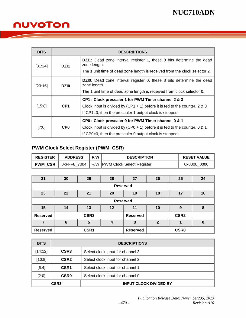
NUC710ADN
Publication Release Date: November235, 2013 - 470 - Revision A10
BITS DESCRIPTIONS
[31:24] DZI1 DZI1: Dead zone interval register 1, these 8 bits determine the dead zone length. The 1 unit time of dead zone length is received from the clock selector 2.
[23:16] DZI0 DZI0: Dead zone interval register 0, these 8 bits determine the dead zone length. The 1 unit time of dead zone length is received from clock selector 0.
[15:8] CP1 CP1 : Clock prescaler 1 for PWM Timer channel 2 & 3 Clock input is divided by (CP1 + 1) before it is fed to the counter. 2 & 3 If CP1=0, then the prescaler 1 output clock is stopped.
[7:0] CP0 CP0 : Clock prescaler 0 for PWM Timer channel 0 & 1 Clock input is divided by (CP0 + 1) before it is fed to the counter. 0 & 1 If CP0=0, then the prescaler 0 output clock is stopped.
PWM Clock Select Register (PWM_CSR)
REGISTER ADDRESS R/W DESCRIPTION RESET VALUE
PWM_CSR 0xFFF8_7004 R/W PWM Clock Select Register 0x0000_0000
31 30 29 28 27 26 25 24
Reserved
23 22 21 20 19 18 17 16
Reserved 15 14 13 12 11 10 9 8
Reserved CSR3 Reserved CSR2 7 6 5 4 3 2 1 0
Reserved CSR1 Reserved CSR0
BITS DESCRIPTIONS
[14:12] CSR3 Select clock input for channel 3
[10:8] CSR2 Select clock input for channel 2.
[6:4] CSR1 Select clock input for channel 1
[2:0] CSR0 Select clock input for channel 0
CSR3 INPUT CLOCK DIVIDED BY

NUC710ADN
Publication Release Date: November23, 2013 - 471 - Revision A10
000 2
001 4
010 8
011 16
100 1
PWM Control Register (PWM_PCR)
REGISTER ADDRESS R/W DESCRIPTION RESET VALUE
PWM_PCR 0xFFF8_7008 R/W PWM Control Register 0x0000_0000
31 30 29 28 27 26 25 24
Reserved
23 22 21 20 19 18 17 16
Reserved PCR19 PCR18 PCR17 PCR16 15 14 13 12 11 10 9 8
PCR15 PCR14 PCR13 PCR12 PCR11 PCR10 PCR09 PCR08 7 6 5 4 3 2 1 0
PCR07 PCR06 PCR05 PCR04 PCR03 PCR02 PCR01 PCR00
BITS DESCRIPTIONS
[19] PCR 19 Channel 3 toggle/one shot mode 1 = Toggle mode 0 = One shot mode
[18] PCR 18 Channel 3 Inverter on/off 1 = Inverter on 0 = Inverter off
[17] PCR 17 Reserved
[16] PCR 16 Channel 3 enable/disable 1 = Enable 0 = Disable
[15] PCR 15 Channel 2 toggle/one shot mode 1 = Toggle mode 0 = One shot mode
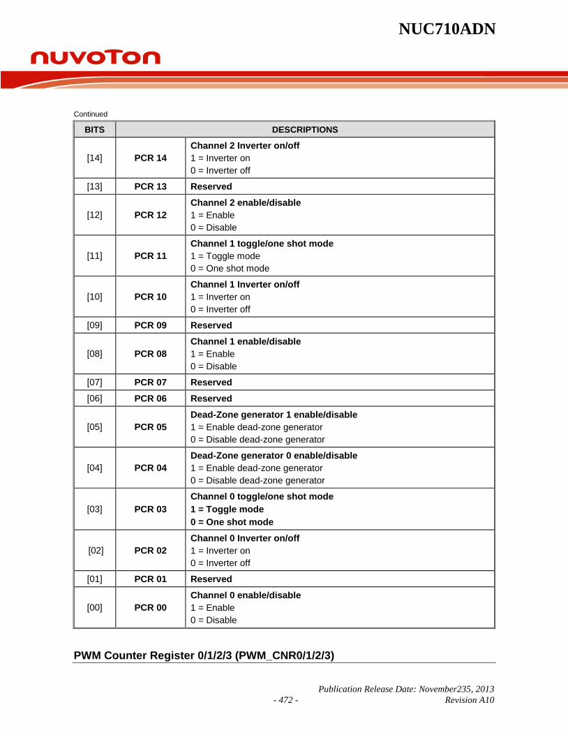
NUC710ADN
Publication Release Date: November235, 2013 - 472 - Revision A10
Continued
BITS DESCRIPTIONS
[14] PCR 14 Channel 2 Inverter on/off 1 = Inverter on 0 = Inverter off
[13] PCR 13 Reserved
[12] PCR 12 Channel 2 enable/disable 1 = Enable 0 = Disable
[11] PCR 11 Channel 1 toggle/one shot mode 1 = Toggle mode 0 = One shot mode
[10] PCR 10 Channel 1 Inverter on/off 1 = Inverter on 0 = Inverter off
[09] PCR 09 Reserved
[08] PCR 08 Channel 1 enable/disable 1 = Enable 0 = Disable
[07] PCR 07 Reserved [06] PCR 06 Reserved
[05] PCR 05 Dead-Zone generator 1 enable/disable 1 = Enable dead-zone generator 0 = Disable dead-zone generator
[04] PCR 04 Dead-Zone generator 0 enable/disable 1 = Enable dead-zone generator 0 = Disable dead-zone generator
[03] PCR 03 Channel 0 toggle/one shot mode 1 = Toggle mode 0 = One shot mode
[02] PCR 02 Channel 0 Inverter on/off 1 = Inverter on 0 = Inverter off
[01] PCR 01 Reserved
[00] PCR 00 Channel 0 enable/disable 1 = Enable 0 = Disable
PWM Counter Register 0/1/2/3 (PWM_CNR0/1/2/3)
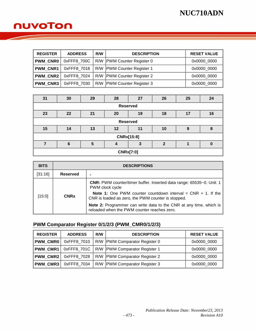
NUC710ADN
Publication Release Date: November23, 2013 - 473 - Revision A10
REGISTER ADDRESS R/W DESCRIPTION RESET VALUE
PWM_CNR0 0xFFF8_700C R/W PWM Counter Register 0 0x0000_0000 PWM_CNR1 0xFFF8_7018 R/W PWM Counter Register 1 0x0000_0000 PWM_CNR2 0xFFF8_7024 R/W PWM Counter Register 2 0x0000_0000 PWM_CNR3 0xFFF8_7030 R/W PWM Counter Register 3 0x0000_0000
31 30 29 28 27 26 25 24
Reserved
23 22 21 20 19 18 17 16
Reserved 15 14 13 12 11 10 9 8
CNRx[15:8] 7 6 5 4 3 2 1 0
CNRx[7:0]
BITS DESCRIPTIONS
[31:16] Reserved -
[15:0] CNRx
CNR: PWM counter/timer buffer. Inserted data range: 65535~0. Unit: 1 PWM clock cycle
Note 1: One PWM counter countdown interval = CNR + 1. If the CNR is loaded as zero, the PWM counter is stopped. Note 2: Programmer can write data to the CNR at any time, which is reloaded when the PWM counter reaches zero.
PWM Comparator Register 0/1/2/3 (PWM_CMR0/1/2/3)
REGISTER ADDRESS R/W DESCRIPTION RESET VALUE
PWM_CMR0 0xFFF8_7010 R/W PWM Comparator Register 0 0x0000_0000 PWM_CMR1 0xFFF8_701C R/W PWM Comparator Register 1 0x0000_0000 PWM_CMR2 0xFFF8_7028 R/W PWM Comparator Register 2 0x0000_0000 PWM_CMR3 0xFFF8_7034 R/W PWM Comparator Register 3 0x0000_0000

NUC710ADN
Publication Release Date: November235, 2013 - 474 - Revision A10
31 30 29 28 27 26 25 24
Reserved 23 22 21 20 19 18 17 16
Reserved 15 14 13 12 11 10 9 8
CMRx[15:8] 7 6 5 4 3 2 1 0
CMRx[7:0]
BITS DESCRIPTIONS
[31:16] Reserved -
[15:0] CMRx
CMR: PWM comparator register Inserted data range: 65535~0. CMR is used to determine PWM output duty ratio. Note 1: PWM duty = CMR + 1.If CMR is loaded as zero, PWM duty = 1 Note 2: Programmer can feel free to write data to CMR at any time, and it is reloaded when PWM counter reaches zero.
PWM Data Register 0/1/2/3 (PWM_PDR 0/1/2/3)
REGISTER ADDRESS R/W DESCRIPTION RESET VALUE PWM_PDR0 0xFFF8_7014 R PWM Data Register 0 0x0000_0000 PWM_PDR1 0xFFF8_7020 R PWM Data Register 1 0x0000_0000 PWM_PDR2 0xFFF8_702C R PWM Data Register 2 0x0000_0000 PWM_PDR3 0xFFF8_7038 R PWM Data Register 3 0x0000_0000
31 30 29 28 27 26 25 24
Reserved
23 22 21 20 19 18 17 16
Reserved 15 14 13 12 11 10 9 8
PDRx[15:8] 7 6 5 4 3 2 1 0
PDRx[7:0]

NUC710ADN
Publication Release Date: November23, 2013 - 475 - Revision A10
BITS DESCRIPTIONS [31:16] Reserved -
[15:0] PDRx PDR: PWM Data register. User can monitor PDR to get current value in 16-bit down counter.
PWM Interrupt Enable Register (PWM_PIER)
REGISTER ADDRESS R/W DESCRIPTION RESET VALUE
PWM_PIER 0xFFF8_703C R/W PWM Interrupt Enable Register 0x0000_0000
31 30 29 28 27 26 25 24
Reserved
23 22 21 20 19 18 17 16
Reserved 15 14 13 12 11 10 9 8
Reserved 7 6 5 4 3 2 1 0
Reserved PIER3 PIER2 PIER1 PIER0
BITS DESCRIPTIONS
[31:4] Reserved -
[3] PIER3 Enable/Disable PWM counter channel 3 interrupt request 1 = Enable 0 = Disable
[2] PIER2 Enable/Disable PWM counter channel 2 interrupt request 1 = Enable 0 = Disable
[1] PIER1 Enable/Disable PWM counter channel 1 interrupt request 1 = Enable 0 = Disable
[0] PIER0 Enable/Disable PWM counter channel 0 interrupt request 1 = Enable 0 = Disable
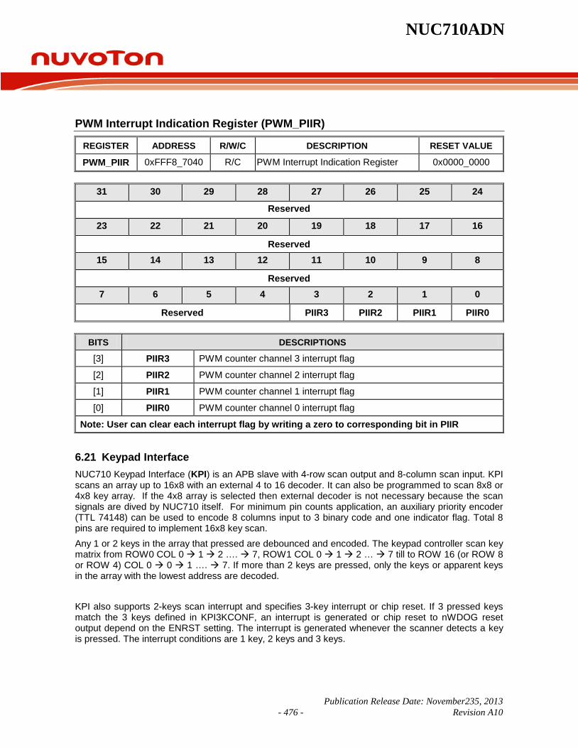
NUC710ADN
Publication Release Date: November235, 2013 - 476 - Revision A10
PWM Interrupt Indication Register (PWM_PIIR)
REGISTER ADDRESS R/W/C DESCRIPTION RESET VALUE
PWM_PIIR 0xFFF8_7040 R/C PWM Interrupt Indication Register 0x0000_0000
31 30 29 28 27 26 25 24
Reserved
23 22 21 20 19 18 17 16
Reserved 15 14 13 12 11 10 9 8
Reserved 7 6 5 4 3 2 1 0
Reserved PIIR3 PIIR2 PIIR1 PIIR0
BITS DESCRIPTIONS
[3] PIIR3 PWM counter channel 3 interrupt flag
[2] PIIR2 PWM counter channel 2 interrupt flag
[1] PIIR1 PWM counter channel 1 interrupt flag
[0] PIIR0 PWM counter channel 0 interrupt flag
Note: User can clear each interrupt flag by writing a zero to corresponding bit in PIIR
6.21 Keypad Interface NUC710 Keypad Interface (KPI) is an APB slave with 4-row scan output and 8-column scan input. KPI scans an array up to 16x8 with an external 4 to 16 decoder. It can also be programmed to scan 8x8 or 4x8 key array. If the 4x8 array is selected then external decoder is not necessary because the scan signals are dived by NUC710 itself. For minimum pin counts application, an auxiliary priority encoder (TTL 74148) can be used to encode 8 columns input to 3 binary code and one indicator flag. Total 8 pins are required to implement 16x8 key scan. Any 1 or 2 keys in the array that pressed are debounced and encoded. The keypad controller scan key matrix from ROW0 COL 0 1 2 …. 7, ROW1 COL 0 1 2 … 7 till to ROW 16 (or ROW 8 or ROW 4) COL 0 0 1 …. 7. If more than 2 keys are pressed, only the keys or apparent keys in the array with the lowest address are decoded.
KPI also supports 2-keys scan interrupt and specifies 3-key interrupt or chip reset. If 3 pressed keys match the 3 keys defined in KPI3KCONF, an interrupt is generated or chip reset to nWDOG reset output depend on the ENRST setting. The interrupt is generated whenever the scanner detects a key is pressed. The interrupt conditions are 1 key, 2 keys and 3 keys.
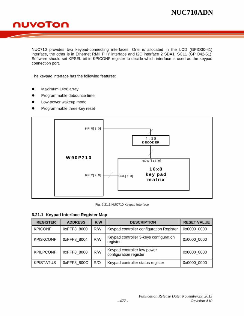
NUC710ADN
Publication Release Date: November23, 2013 - 477 - Revision A10
NUC710 provides two keypad-connecting interfaces. One is allocated in the LCD (GPIO30-41) interface, the other is in Ethernet RMII PHY interface and I2C interface 2 SDA1, SCL1 (GPIO42-51). Software should set KPSEL bit in KPICONF register to decide which interface is used as the keypad connection port. The keypad interface has the following features: Maximum 16x8 array Programmable debounce time Low-power wakeup mode Programmable three-key reset
W90P710
4 :16DECODER
ROW[[16:0]
KPIC[7:0]
KPIR[3:0]
COL[7:0]
16x8key padmatrix
Fig. 6.21.1 NUC710 Keypad Interface
6.21.1 Keypad Interface Register Map
REGISTER ADDRESS R/W DESCRIPTION RESET VALUE
KPICONF 0xFFF8_8000 R/W Keypad controller configuration Register 0x0000_0000
KPI3KCONF 0xFFF8_8004 R/W Keypad controller 3-keys configuration register 0x0000_0000
KPILPCONF 0xFFF8_8008 R/W Keypad controller low power configuration register 0x0000_0000
KPISTATUS 0xFFF8_800C R/O Keypad controller status register 0x0000_0000

NUC710ADN
Publication Release Date: November235, 2013 - 478 - Revision A10
6.21.2 Register Description
Keypad Controller Configuration Register (KPI_CONF)
REGISTER ADDRESS R/W DESCRIPTION RESET VALUE
KPICONF 0xFFF8_8000 R/O Keypad configuration register 0x0000_0000
31 30 29 28 27 26 25 24
RESERVED
23 22 21 20 19 18 17 16
RESERVED ENCODE ODEN KPSEL ENKP KSIZE
15 14 13 12 11 10 9 8
DBTC
7 6 5 4 3 2 1 0
PRESCALE
BITS DESCRIPTION
[31:22] RESERVED -
[21] ENCODE
Enable Encode Function If an auxiliary 8 to 3 encoder is used to minimize keypad interface pin counts, user can connect encoder data to KPCOL [2:0] and indicator flag (low active) to KPCOL [3]. 1 = Enable encoder function 0 = Default. (8 column inputs)
[20] ODEN
Open Drain Enable If there is more than one key pressed in the same column, then a “short-circuit” occurs between the active scan and inactive scan row. Software can set this bit HIGH to enable scan output KPROW [3:0] pins work as “open-drain” to avoid the “short-circuit”. 1 = Open drain 0 = Push-pull driver
[19] KPSEL
Keypad select NUC710 provide two interfaces for keypad function. Software should set this bit to select which interface is used to connect the keypad matrix. 1 = Pin #23 ~34 is used as keypad interface 0 = Pin #81~88 and #19, #20 are used as keypad interface
NUC710ADN
Publication Release Date: November23, 2013 - 479 - Revision A10
Continued
BITS DESCRIPTION
[18] ENKP
Keypad scan enable Setting this bit high enable the key scan function. 1 = Enable keypad scan 0 = Disable keypad scan
[17:16] KSIZE
Key array size
KSIZE Key array size
2’b00 4x8, 3x8, 2x8, 1x8
2’b01 8x8, 7x8, 6x8, 5x8
2’b1x 16x8, 15x8, 14x8, 13x8, 12x8, 11x8, 10x8, 9x8
[15:8] DBTC
Debounce terminal count Debounce counter counts the number of consecutive scans that decoded the same keys. When the debounce counter is equal to the terminal count it will generate a key scan interrupt.
[7:0] PRESCALE
Row scan cycle pre-scale value This value is used to prescale row scan cycle. The prescale counter is clocked by 0.9375MHz clock. Key array scan time = 1.067us x PRESCALE x16 ROWS The following example is the scan time for PRESCALE = 0xFA Tscan_time = 1.067us x 250 x16 = 4.268ms If debounce terminal count = 0x05, a key detection interrupt is fired in approximately 21.34ms. The array scan time can range from 17.07us to 1.118 sec.

NUC710ADN
Publication Release Date: November235, 2013 - 480 - Revision A10
COL[0]COL[1]COL[2]COL[3]
A0A1A2GS
16x8 keys matrix
ROW[15:0] COL[7:0]
IN[7:0]
74148
ENCODER
74138
ROW[3:0]
W90P710
keypad I/F with 8:3 encoder
Fig. 6.21.1 Keypad Interface with row decoder and column encoder
Keypad Controller 3-keys Configuration Register (KPI3KCONF)
REGISTER ADDRESS R/W DESCRIPTION RESET VALUE
KPI3KCONF 0xFFF8_8004 W/R three-key configuration register 0x0000_0000
31 30 29 28 27 26 25 24
RESERVED EN3KY ENRST
23 22 21 20 19 18 17 16
RESERVED K32R K32C
15 14 13 12 11 10 9 8
RESERVED K31R K31C
7 6 5 4 3 2 1 0
RESERVED K30R K30C

NUC710ADN
Publication Release Date: November23, 2013 - 481 - Revision A10
BITS DESCRIPTION
[31:26] RESERVED -
[25] EN3KY Enable three-keys detection Setting this bit enables hardware to detect 3 keys specified by software
[24] ENRST
Enable three-key reset Setting this bit enable hardware reset when the three-keys are detected.
EN3KY ENRST Function
0 X three-key function is disabled
1 0 generate three-key interrupt
1 1 hardware reset by three-key-reset
[23] RESERVED -
[22:19] K32R The #2 key row address The #2 means the row address and the column address is the highest of the specified 3-kyes.
[18:16] K32C The #2 key column address
[15] RESERVED -
[14:11] K31R The #1 key row address The #1 means the row address and the column address is the 2nd of the specified 3-kyes.
[10:8] K31C The #1 key column address [7] RESERVED -
[6:3] K30R The #0 key row address The #0 means the row address and the column address is the lowest of the specified 3-kyes.
[2:0] K30C The #0 key column address
Application Note: Due to hardware scan from row[0], col[0], row[0], col[1], …, to row[15], col[7] the K30R,K30C should be filled the lowest address of the three-keys. For example, if 2,0 4,6, 1,3 keys are defined as three-keys. Software should set K30R, K30C = 1, 3, K31R, K31C = 2, 0 and K32R, K32C = 4, 6.

NUC710ADN
Publication Release Date: November235, 2013 - 482 - Revision A10
keypad Interface Low Power Mode Configuration Register (KPILPCONF)
REGISTER ADDRESS R/W DESCRIPTION RESET VALUE
KPILPCOF 0xFFF8_8008 R/W Low power configuration register 0x0000_0000
31 30 29 28 27 26 25 24
RESERVED
23 22 21 20 19 18 17 16
WAKE
15 14 13 12 11 10 9 8
LPWCEN
7 6 5 4 3 2 1 0
RESERVED LPWR
BITS DESCRIPTION
[31:17] RESERVED -
[16] WAKE
Lower power wakeup enable Setting this bit enables low power wakeup 1 = Wakeup enable 0 = Not enable
[15:8] LPWCEN
Low power wakeup column enable Specify columns for low power wakeup. For example, if user wants to use keys in row N and column 0, 2, 5 to wake up NUC710, then the LPWCEN should be fill 8’b00100101. Application restriction: when ENCODE=1 case, LPWCEN should be set as 0xFF i.e., all columns in specified row are used as wake up input. In this case, user cannot specify special column(s) to wake up NUC710.
[7:4] RESERVED -
[3:0] LPWR
Low power wakeup row address Define the row address keys used to wakeup. For 16x8 or 8x8 (with 4:16 or 3:8 decoder) keypad key configuration, LPWR means “Hex” code but for 4x8 (without decoder), LPWR means “binary” code. For example, if the user wants to use all keys on row 3 of 16x8 keypad to wakeup NUC710, then 0x3 should be fill into this register but for 4x8 keypad it should be filled as 4’b1000.

NUC710ADN
Publication Release Date: November23, 2013 - 483 - Revision A10
Keypad Interface Status Register (KPISTATUS)
REGISTER ADDRESS R/W DESCRIPTION RESET VALUE
KPISTATUS 0xFFF8_800C R/O Keypad status register 0x0000_0000
31 30 29 28 27 26 25 24
RESERVED
23 22 21 20 19 18 17 16
RESERVED INT 3KRST PDWAKE 3KEY 2KEY 1KEY
15 14 13 12 11 10 9 8
RESERVED KEY1R KEY1C
7 6 5 4 3 2 1 0
RESERVED KEY0R KEY0C
BITS DESCRIPTION
[31:22] RESERVED -
[21] INT
Key interrupt This bit indicates the key scan interrupt is active and that one or two keys have changed status. The interrupt also occur when the three specified keys are detected if ENRST bit in KPI3KFCON is cleared. It is cleared by hardware automatically when software read KPISTATUS register.
[20] 3KRST
3-Keys reset flag This bit is a record flag for software reference; it is set after a 3-key reset. 1 = 3 keys reset 0 = No reset. This bit is cleared while it is read.
[19] PDWAKE
Power Down Wakeup flag This flag indicates the chip is wakeup from power down by keypad 1 = Wakeup up by keypad 0 = No wakeup
[18] 3KEY
Specified three-key is detected. This flag indicates specified-three-keys were detected. Software can read this bit to know the keypad interrupt is 3 keys or not.

NUC710ADN
Publication Release Date: November235, 2013 - 484 - Revision A10
Continued
BITS DESCRIPTION
[17] 2KEY
Double-key press This bit indicates that 2 keys have been detected. Software can read KEY1R, KEY1C and KEY0R, KEY0C to know which two keys are pressed.
[16] 1KEY Single-key press This bit indicates that 1 key has been detected. Software can read KEY0R, KEY0C to know which key is pressed.
[15] RESERVED -
[14:11] KEY1R
KEY1 row address This value indicates key1 row address. The keypad controller scan keypad matrix from row 0, column0 1 2 …. 7 and then row1 column 0 1 2 7 so the lowest key address is stored in KEY0R, KEY0C. This register stores the 2nd address, if more than one key is pressed.
[10:8] KEY1C KEY1 column address This value indicates key1 column address..
[7] RESERVED -
[6:3] KEY0R
KEY1 row address This value indicates key0 row address. This value indicates key0 row address. This value indicates key1 row address. The keypad controller scan keypad matrix from row 0, column0 1 2 …. 7 and then row1 col 0 1 2 … 7 still to row16 (or 8, or 4) column 0 1 2 ….. 7 so the lowest key address is stored in KEY0R, KEY0C.
[2:0] KEY0C KEY1 column address This value indicates key0 row address.
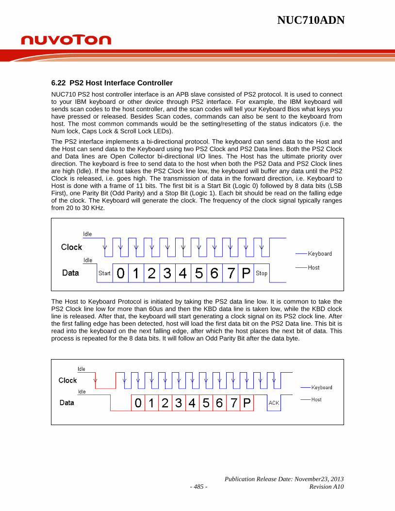
NUC710ADN
Publication Release Date: November23, 2013 - 485 - Revision A10
6.22 PS2 Host Interface Controller NUC710 PS2 host controller interface is an APB slave consisted of PS2 protocol. It is used to connect to your IBM keyboard or other device through PS2 interface. For example, the IBM keyboard will sends scan codes to the host controller, and the scan codes will tell your Keyboard Bios what keys you have pressed or released. Besides Scan codes, commands can also be sent to the keyboard from host. The most common commands would be the setting/resetting of the status indicators (i.e. the Num lock, Caps Lock & Scroll Lock LEDs). The PS2 interface implements a bi-directional protocol. The keyboard can send data to the Host and the Host can send data to the Keyboard using two PS2 Clock and PS2 Data lines. Both the PS2 Clock and Data lines are Open Collector bi-directional I/O lines. The Host has the ultimate priority over direction. The keyboard is free to send data to the host when both the PS2 Data and PS2 Clock lines are high (Idle). If the host takes the PS2 Clock line low, the keyboard will buffer any data until the PS2 Clock is released, i.e. goes high. The transmission of data in the forward direction, i.e. Keyboard to Host is done with a frame of 11 bits. The first bit is a Start Bit (Logic 0) followed by 8 data bits (LSB First), one Parity Bit (Odd Parity) and a Stop Bit (Logic 1). Each bit should be read on the falling edge of the clock. The Keyboard will generate the clock. The frequency of the clock signal typically ranges from 20 to 30 KHz.
The Host to Keyboard Protocol is initiated by taking the PS2 data line low. It is common to take the PS2 Clock line low for more than 60us and then the KBD data line is taken low, while the KBD clock line is released. After that, the keyboard will start generating a clock signal on its PS2 clock line. After the first falling edge has been detected, host will load the first data bit on the PS2 Data line. This bit is read into the keyboard on the next falling edge, after which the host places the next bit of data. This process is repeated for the 8 data bits. It will follow an Odd Parity Bit after the data byte.
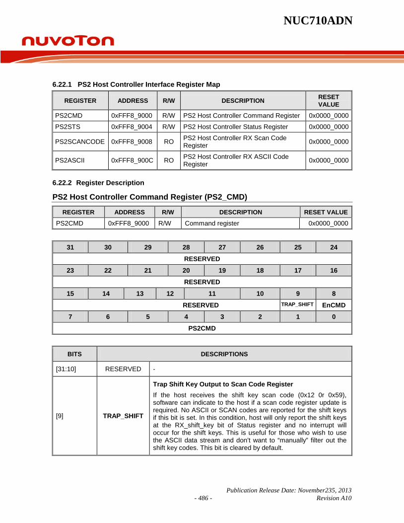
NUC710ADN
Publication Release Date: November235, 2013 - 486 - Revision A10
6.22.1 PS2 Host Controller Interface Register Map
REGISTER ADDRESS R/W DESCRIPTION RESET VALUE
PS2CMD 0xFFF8_9000 R/W PS2 Host Controller Command Register 0x0000_0000
PS2STS 0xFFF8_9004 R/W PS2 Host Controller Status Register 0x0000_0000
PS2SCANCODE 0xFFF8_9008 RO PS2 Host Controller RX Scan Code Register 0x0000_0000
PS2ASCII 0xFFF8_900C RO PS2 Host Controller RX ASCII Code Register 0x0000_0000
6.22.2 Register Description
PS2 Host Controller Command Register (PS2_CMD)
REGISTER ADDRESS R/W DESCRIPTION RESET VALUE
PS2CMD 0xFFF8_9000 R/W Command register 0x0000_0000
31 30 29 28 27 26 25 24
RESERVED
23 22 21 20 19 18 17 16
RESERVED
15 14 13 12 11 10 9 8
RESERVED TRAP_SHIFT EnCMD
7 6 5 4 3 2 1 0
PS2CMD
BITS DESCRIPTIONS
[31:10] RESERVED -
[9] TRAP_SHIFT
Trap Shift Key Output to Scan Code Register If the host receives the shift key scan code (0x12 0r 0x59), software can indicate to the host if a scan code register update is required. No ASCII or SCAN codes are reported for the shift keys if this bit is set. In this condition, host will only report the shift keys at the RX_shift_key bit of Status register and no interrupt will occur for the shift keys. This is useful for those who wish to use the ASCII data stream and don’t want to “manually” filter out the shift key codes. This bit is cleared by default.
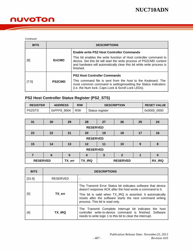
NUC710ADN
Publication Release Date: November23, 2013 - 487 - Revision A10
Continued
BITS DESCRIPTIONS
[8] EnCMD
Enable write PS2 Host Controller Commands This bit enables the write function of Host controller command to device. Set this bit will start the write process of PS2CMD content and hardware will automatically clear this bit while write process is finished.
[7:0] PS2CMD
PS2 Host Controller Commands This command file is sent from the host to the Keyboard. The most common command is setting/resetting the Status Indicators (i.e. the Num lock, Caps Lock & Scroll Lock LEDs).
PS2 Host Controller Status Register (PS2_STS)
REGISTER ADDRESS R/W DESCRIPTION RESET VALUE
PS2STS 0xFFF8_9004 R/W Status register 0x0000_0000
31 30 29 28 27 26 25 24
RESERVED
23 22 21 20 19 18 17 16
RESERVED
15 14 13 12 11 10 9 8
RESERVED
7 6 5 4 3 2 1 0
RESERVED TX_err TX_IRQ RESERVED RX_IRQ
BITS DESCRIPTIONS
[31:6] RESERVED -
[5] TX_err
The Transmit Error Status bit indicates software that device doesn’t response ACK after the host wrote a command to it. This bit is valid when TX_IRQ is asserted. It automatically resets after the software starts the next command writing process. This bit is read only.
[4] TX_IRQ The Transmit Complete Interrupt bit indicates the host controller write-to-device command is finished. Software needs to write logic 1 to this bit to clear the interrupt.

NUC710ADN
Publication Release Date: November235, 2013 - 488 - Revision A10
Continued
BITS DESCRIPTIONS
[3:1] - Reserved
[0] RX_IRQ
The Receive Interrupt bit indicates the host controller received one byte of data from the device. This data is stored at PS2_SCANCODE register. The software needs to write 1 to this bit to clear the interrupt after receiving data in the RX_SCAN_CODE register. Note that the reception of the Extend (0xE0) and Release (0xF0) scan code does not trigger a host interrupt. Shift key codes are determined by the TRAP_SHIFT bit of the PS2_CMD register.
PS2 Host Controller RX Scan Code Register (PS2_SCANCODE)
REGISTER ADDRESS R/W DESCRIPTION RESET VALUE
PS2SCANCODE 0xFFFF_9008 R/W RX Scan Code Register 0x0000_0000
31 30 29 28 27 26 25 24
RESERVED
23 22 21 20 19 18 17 16
RESERVED
15 14 13 12 11 10 9 8
RESERVED RX_shift_key RX_release RX_extend
7 6 5 4 3 2 1 0
RX_SCAN_CODE
BITS DESCRIPTIONS
[31:11] RESERVED -
[10] RX_shift_key The Receive Shift Key bit indicates the left or right shift key on the keyboard is held. This bit is read only and is cleared by the host when the release shift key codes are received.
[9] RX_release
Receive Released Byte When a key is released, the keyboard sends F0 (hex) to inform the host controller. This bit indicates the host controller received the release byte (F0). This bit is read only and updates when the host has received the next data byte.

NUC710ADN
Publication Release Date: November23, 2013 - 489 - Revision A10
Continued
BITS DESCRIPTIONS
[8] RX_extend
Receive Extended Byte A handful of keys on keyboard are extended keys and thus require two more scan codes. These keys are preceded by E0 (hex). This bit indicates the host controller received an extended byte (E0). This bit is read only and updates when the host has received the next data byte.
[7:0] RX_SCAN_CODE
PS2 Host Controller Received Data Field This field stores the original data content transmitted from the device. This field is valid when RX_IRQ is asserted. Note that the host does not report “Extend” or “Release” scan codes to this field and does not generate interrupts if they are received by host, i.e. 0xE0 and 0xF0. The case of the shift key codes is determined by the TRAP_SHIFT bit of PS2_CMD register.
PS2 Host Controller RX ASCII Code Register (PS2_ASCII)
REGISTER ADDRESS R/W DESCRIPTION RESET VALUE
PS2ASCII 0xFFF8_900C R/W RX ASCII Code Register 0x0000_0000
31 30 29 28 27 26 25 24
RESERVED
23 22 21 20 19 18 17 16
RESERVED
15 14 13 12 11 10 9 8
RESERVED
7 6 5 4 3 2 1 0
RX_ASCII_CODE
BITS DESCRIPTIONS
[31:8] RESERVED -
[7:0] RX_ASCII_CODE
PS2 Host Controller Received Data Field This field stores the ASCII data content transmitted from device. Therefore, this part translates the scan code into an ASCII value. It is read as 0x2E when there is no ASCII code mapped to the scan code stored in RX_SCAN_CODE register. This field is valid when RX_IRQ is asserted.
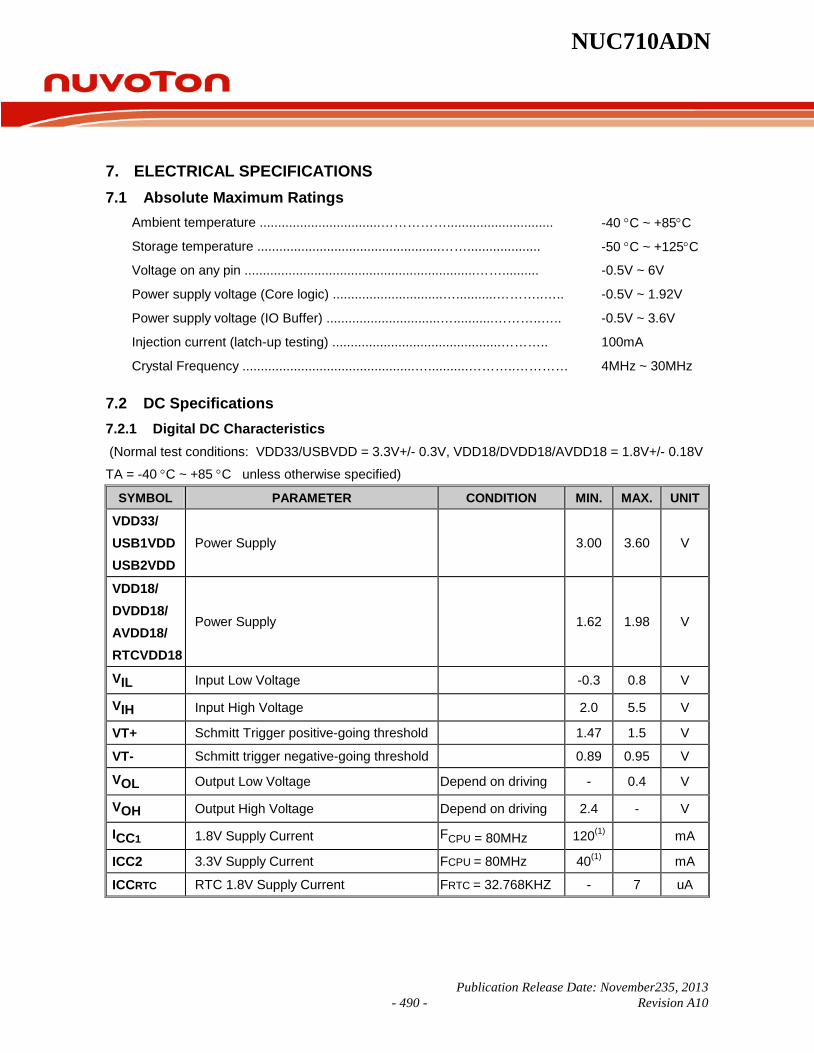
NUC710ADN
Publication Release Date: November235, 2013 - 490 - Revision A10
7. ELECTRICAL SPECIFICATIONS 7.1 Absolute Maximum Ratings
Ambient temperature .................................……………............................. -40 °C ~ +85°C
Storage temperature ..................................................…….................... -50 °C ~ +125°C
Voltage on any pin ...............................................................…….......... -0.5V ~ 6V
Power supply voltage (Core logic) ..............................…...........………..….. -0.5V ~ 1.92V
Power supply voltage (IO Buffer) ...............................…...........………..….. -0.5V ~ 3.6V
Injection current (latch-up testing) ..............................................……….. 100mA
Crystal Frequency ...............................................…...........………..………… 4MHz ~ 30MHz
7.2 DC Specifications 7.2.1 Digital DC Characteristics (Normal test conditions: VDD33/USBVDD = 3.3V+/- 0.3V, VDD18/DVDD18/AVDD18 = 1.8V+/- 0.18V
TA = -40 °C ~ +85 °C unless otherwise specified)
SYMBOL PARAMETER CONDITION MIN. MAX. UNIT
VDD33/ USB1VDD USB2VDD
Power Supply 3.00 3.60 V
VDD18/ DVDD18/ AVDD18/ RTCVDD18
Power Supply 1.62 1.98 V
VIL Input Low Voltage -0.3 0.8 V
VIH Input High Voltage 2.0 5.5 V
VT+ Schmitt Trigger positive-going threshold 1.47 1.5 V
VT- Schmitt trigger negative-going threshold 0.89 0.95 V
VOL Output Low Voltage Depend on driving - 0.4 V
VOH Output High Voltage Depend on driving 2.4 - V
ICC1 1.8V Supply Current FCPU = 80MHz 120(1) mA
ICC2 3.3V Supply Current FCPU = 80MHz 40(1) mA
ICCRTC RTC 1.8V Supply Current FRTC = 32.768KHZ - 7 uA

NUC710ADN
Publication Release Date: November23, 2013 - 491 - Revision A10
Digital DC Characteristics, continued
SYMBOL PARAMETER CONDITION MIN. MAX. UNIT
IPD1 1.8V Supply Current, Power down mode 11(2) - uA
IPD2 3.3V Supply Current, Power down mode All IOs are connected to 3.3V or 0V
1(3) - uA
IIH Input High Current VIN = 2.4 V -1 1 µA
IIL Input Low Current VIN = 0.4 V -1 1 µA
IIHP Input High Current (pull-up) VIN = 2.4 V -15 -10 µA
IILP Input Low Current (pull-up) VIN = 0.4 V -55 -25 µA
IIHD Input High Current (pull-down) VIN = 2.4 V 25 60 µA
IILD Input Low Current (pull-down) VIN = 0.4 V 5 10 µA
NOTE: 1. The operation current is measured in room temperature and run SDRAM read/write test program
only. All IPs’ clocks are enabled.
2. Both USB transceivers are disabled and D15-D8 for power-on setting are connected to 3.3V

NUC710ADN
Publication Release Date: November235, 2013 - 492 - Revision A10
Table 7.2.1TSMC IO DC Characteristics
PARAMETER MIN. TYP. MAX.
VIL Input Low Voltage -0.3V 0.8V
VIIHH Input High Voltage 2V 5.5V
VT Threshold point 1.46V 1.59V 1.75V
VT+ Schmitt trig low to high threshold point 1.47V 1.50V 1.50V
VT- Schmitt trig, high to low threshold point 0.90V 0.94V 0.96V
II Input leakage current @VI= 3.3V or 0V +/- 10uA
Ioz Tri-state output leakage current @Vo =3.3V or 0V +/- 10UA
RPU Pull-up resistor 44KΩ 66KΩ 110KΩ
RPD Pull-down resistor 25KΩ 50KΩ 110KΩ
VOL Output low voltage @IOL(min) 0.4V
VOH Output high voltage @IOH (min) 2.4V
IOL
Low level output current @VOL = 0.4V 4mA 4.9mA 7.4mA 9.8mA
Low level output current @VOL = 0.4V 8mA 9.7mA 14.9mA 19.5mA
Low level output current @VOL = 0.4V 12mA 14.6mA 22.3mA 29.3mA
IOH
High level output current @VOH = 2.4V 4mA 6.3mA 12.8mA 21.2mA
High level output current @VOH = 2.4V 8mA 12.7mA 25.6mA 42.4mA
High level output current @VOH = 2.4V 12mA 19.0mA 38.4mA 63.6mA
NOTE: The values in this table are copied from TSMC 1P5M IO library tpz937g_240b silicon report. This table is just for reference. For a more precise DC value, refer to the Alpha-Test result.

NUC710ADN
Publication Release Date: November23, 2013 - 493 - Revision A10
7.2.2 USB Transceiver DC Characteristics
SYMBOL PARAMETER CONDITIONS MIN. MAX. UNIT
VDI Differential Input Sensitivity DP − DM 0.2 V
VCM Differential Common Mode Range Includes VDI range 0.8 2.5 V
VSE Single Ended Receiver Threshold 0.8 2.0 V
VOL Static Output Low Voltage RL of 1.5 KΩ to 3.6 V 0.3 V
VOH Static Output High Voltage RL of 15 KΩ to VSS 2.8 3.6 V
VCRS Output Signal Crossover Voltage 1.3 2.0 V
ZDRV Driver Output Resistance Steady state drive 28 43 Ω
CIN Pin Capacitance 20 pF
7.3 AC Specifications 7.3.1 EBI/SDRAM Interface AC Characteristics
TDHTDSU
1.5V
Output Valid
Intput Valid1.5V
1.5V
1.5V
MCLK
MCLK
D[31:0]
D[31:0]
SDRAM input to W90P710
W90P710 write to SDRAM
TDO
SYMBOL PARAMETER MIN. MAX. UNIT
TDSU D [31:0] Setup Time 2 ns
TDH D [31:0] Hold Time 2 ns
TDO D [31:0], A [24:0], nSCS [1:0], SDQM [3:0], CKE, nSWE, nSRAS, nSCAS 2 7 ns

NUC710ADN
Publication Release Date: November235, 2013 - 494 - Revision A10
7.3.2 EBI/(ROM/SRAM/External I/O) AC Characteristics
Address Valid
R Data
Write Data Vaild
MCLK
TDO
nECS[3:0]
A[21:0]
nOE
D[31:0]
nWAIT
nWBE[3:0]
D[31:0]
TNECSO TNECSO
TADDO
TNOEO TNOEO
TDSU TDH
TNWAH
TNWBO TNWBO
TNWASU
SYMBOL DESCRIPTION MIN MAX UNIT
TADDO Address Output Delay Time 2 7 ns
TNCSO ROM/SRAM/Flash or External I/O Chip Select Delay Time 2 7 ns
TNOEO ROM/SRAM or External I/O Bank Output Enable Delay 2 7 ns
TNWBO ROM/SRAM or External I/O Bank Write Byte Enable Delay 2 7 ns
TDH Read Data Hold Time 0 ns
TDSU Read Data Setup Time 7 ns
TDO Write Data Output Delay Time (SRAM or External I/O) 2 7 ns
TNWASU External Wait Setup Time 3 ns
TNWAH External Wait Hold Time 1 ns

NUC710ADN
Publication Release Date: November23, 2013 - 495 - Revision A10
7.3.3 USB Transceiver AC Characteristics
Low Speed: 75ns at CL = 50pF, 300ns at CL = 350pFFull Speed: 4 to 20ns at CL = 50pF
DifferentialData Lines
10%
Rise Time
90%
Fall Time
tFtR
10%
90%CL
CL
Data Signal Rise and Fall Time
USB Transceiver AC Characteristics
SYMBOL DESCRIPTION CONDITIONS MIN MAX UNIT
TR Rise Time CL = 50 pF 4 20 ns
TF Fall Time CL = 50 pF 4 20 ns
TRFM Rise/Fall Time Matching 90 110 %
TDRATE Full Speed Data Rate Average bit rate
(12 Mb/s ± 0.25%) 11.97 12.03 Mbps

NUC710ADN
Publication Release Date: November235, 2013 - 496 - Revision A10
7.3.4 EMC RMII AC Characteristics Signal timing characteristics conforms to guidelines specified in IEEE Std. 802.3.
PHY_REFCLK
PHY_TXENPHY_TXD[1:0]
TTXO
valid data
TTXH
TFREQ
TRXS TRXHPHY_RXERRPHY_RXD[1:0]PHY_CRSDV
TDUTY
valid data
SYMBOL DESCRIPTION MIN TYP MAX UNIT
TFREQ RMII reference clock frequency 50 MHz
TDUTY RMII clock duty 35% 50% 65% ns
TTXO Transmit data output delay 5 - 15 ns
TTXH Transmit data hold time 2 - - ns
TRXS Receive data setup time 4 - - ns
TRXH Receive data hold time 2 - - ns

NUC710ADN
Publication Release Date: November23, 2013 - 497 - Revision A10
PHY_MDC
PHY_MDIO (Write)
TMDO
valid data
TMDH
valid data
TMDSTMDH
PHY_MDIO(Read)
SYMBOL DESCRIPTION MIN MAX UNIT
TMDO MDIO Output Delay Time 0 15 ns
TMDSU MDIO Setup Time 5 ns
TMDH MDIO Hold Time 5 ns

NUC710ADN
Publication Release Date: November235, 2013 - 498 - Revision A10
7.3.5 LCD Interface AC Characteristics
THOLDTDELAY
VCLK
VSYNCHSYNCVDENVD[23:0]
TPIXCLK
valid data
SYMBOLS DESCRIPTION MIN MAX UNIT
TPIXCLK Pixel clock frequency - 40 MHz
TDELAY VSYNC, HSYNC, VDEN and VD [23:0] output delay from VCLK rising edge 5 15 ns
THOLD VSYNC, HSYNC, VDEN and VD [23:0] output data hold time from VCLK rising edge 0 5 ns
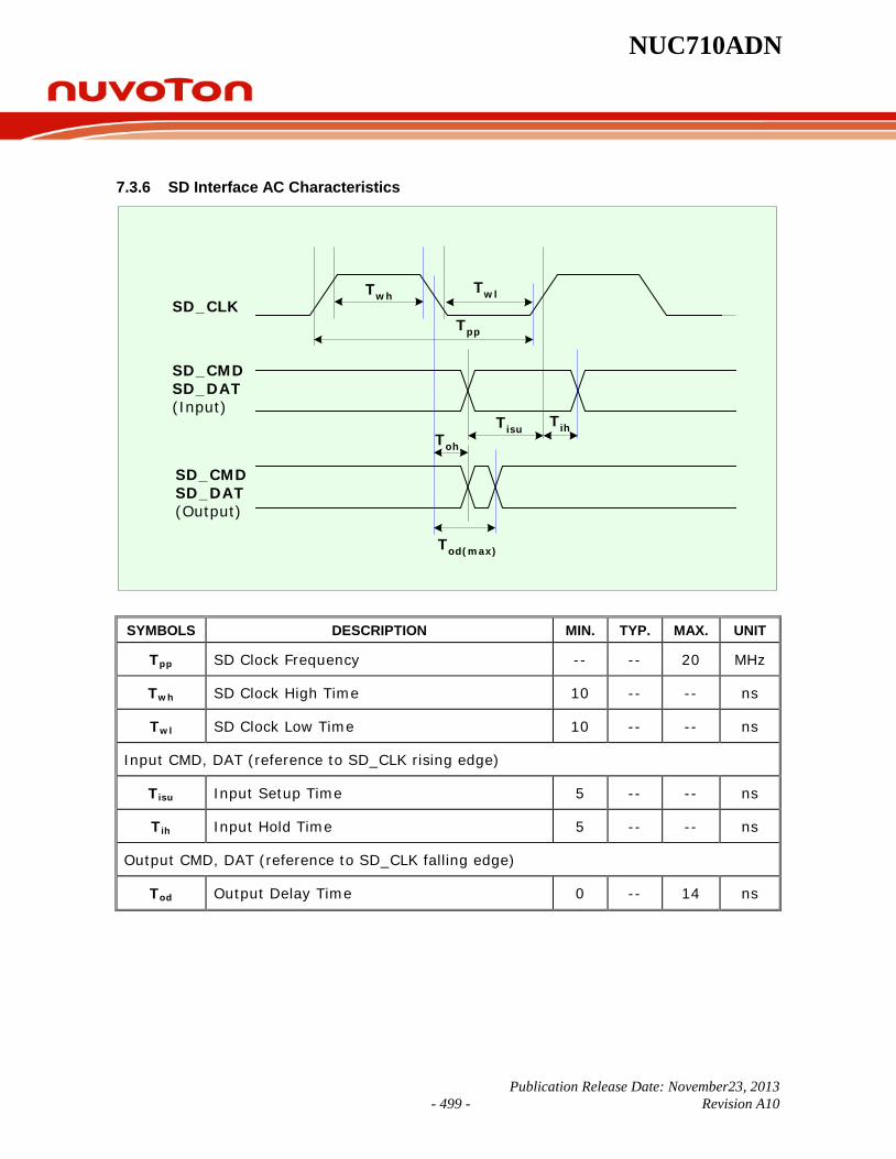
NUC710ADN
Publication Release Date: November23, 2013 - 499 - Revision A10
7.3.6 SD Interface AC Characteristics
Twh
Tpp
Twl
Tisu Tih
Tod(max)
Toh
SD_CLK
SD_CMDSD_DAT(Input)
SD_CMDSD_DAT(Output)
SYMBOLS DESCRIPTION MIN. TYP. MAX. UNIT
Tpp SD Clock Frequency -- -- 20 MHz
Twh SD Clock High Time 10 -- -- ns
Twl SD Clock Low Time 10 -- -- ns
Input CMD, DAT (reference to SD_CLK rising edge)
Tisu Input Setup Time 5 -- -- ns
Tih Input Hold Time 5 -- -- ns
Output CMD, DAT (reference to SD_CLK falling edge)
Tod Output Delay Time 0 -- 14 ns

NUC710ADN
Publication Release Date: November235, 2013 - 500 - Revision A10
7.3.7 AC97/I2S Interface AC Characteristics
TISU
TOD
TIHD TOH
AC97_BCLK
AC97_DATAOAC97_SYNC
AC97_DATAI
TCLK_PERIOD
SYMBOLS DESCRIPTION MIN TYP. MAX UNIT
TCLK_PERIOD AC97 Bit Clock Frequency -- 12.288 -- MHz
TOD AC97_DATAO and AC97_SYNC output delay from AC97_BCLK rising edge -- -- 30 ns
TOH AC97_DATAO and AC97_SYNC output hold time from AC97_BCLK rising edge 5 -- -- ns
TISU AC97_DATAI input setup time to AC97_BCLK falling edge 10 -- -- ns
TIHD AC97_DATAI input hold time from AC97_BCLK falling edge 5 -- -- ns

NUC710ADN
Publication Release Date: November23, 2013 - 501 - Revision A10
TDIS TDIHTDOH
Tout_delay
TBCLK_PERIOD
I2S_BCLK
I2S_DATAOI2S_RLCLK
I2S_DATAI
SYMBOLS DESCRIPTION MIN MAX UNIT
TBCLK_PERIOD IIS Bit Clock Frequency
Note: depending on codec specifications. and register settings
MHz
Tout_delay IIS_DATAO and IIS_RLCLK output delay from IIS_BCLK falling edge -- 30 ns
TDOH IIS_DATAO and IIS_RLCLK data output hold time from IIS_BCLK falling edge 0 -- ns
TDIS IIS_DATAI input setup time to IIS_BCLK rising edge 10 -- ns
TDIH IIS_DATAI input hold time from IIS_BCLK rising edge 100 -- ns

NUC710ADN
Publication Release Date: November235, 2013 - 502 - Revision A10
7.3.8 Smart Card Interface AC Characteristics
Tclk_dat
Tclkh Tclkl
FSC Tclk_rst
SC_RST
SC_CLK
SC_DAT
TR TF
SYMBOL DESCRIPTION CONDITION MIN TYP MAX UNIT
TR and TF for RST Rising and falling time of RST signal
CL = 30pF (Max) 0.8 us
TR and TF for CLK Rising and falling time of CLK signal
CL = 30pF (Max) 4
8% of clock period
TR and TF for DAT (Transmit)
Rising and falling time of DAT signal in transmission mode
CL = 30pF (Max) 0.8 us
TR and TF for DAT (Receive)
Rising and falling time of DAT signal in receive mode 1.2 us
FSC Smart card clock frequency 1 2.5 20 MHz
Tclkh Smart card clock high time 40% 50% 60% clock
Tclkl Smart card clock low time 40% 50% 60% clock
Tclk_dat DAT output delay from SC_CLK falling edge 5 - 20 ns
Tclk_rst RST output delay from SC_CLK falling edge 5 - 10 ns

NUC710ADN
Publication Release Date: November23, 2013 - 503 - Revision A10
7.3.9 I2C Interface AC Characteristics
TSU:STO
TSU:DAT2
TLOWTHIGH
Thd:DAT
TSU:DAT
Thd:STASCL
SDA
SCL
SDA
TSU:SAT
SYMBOL DESCRIPTION MIN MAX UNIT
THIGH I2C Clock high time 1 - us
TLOW I2C clock low time 1 - us
Thd:STA Start condition hold time 1 - us
TSU:DAT Receive data setup time 0.1 - us
Transmit data output delay - 0.5 us
THD:DAT Receive data hold time 1 - us
Transmit data hold time 0 0.9 us
TSU:DAT2 SDA setup time (before STOP condition) 0.5 - us
TSU:STO Stop condition setup time 1 - us
TSU:STA Restart condition setup time 1.5 - us
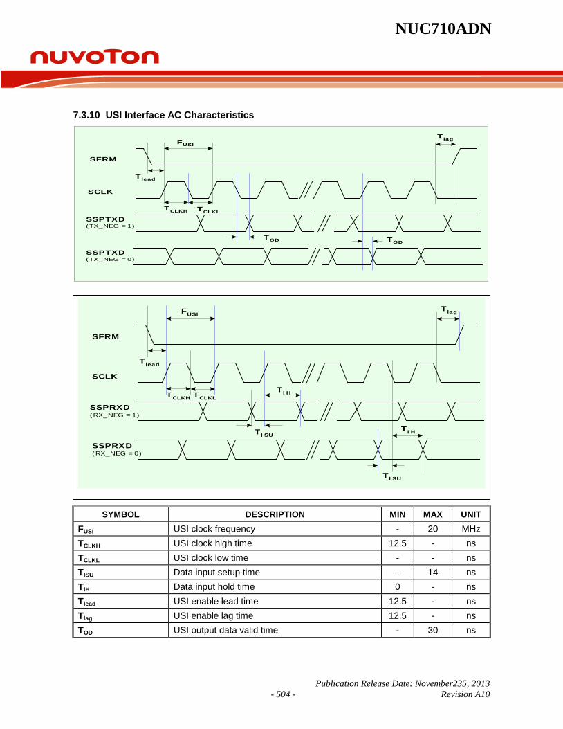
NUC710ADN
Publication Release Date: November235, 2013 - 504 - Revision A10
7.3.10 USI Interface AC Characteristics
Tlag
TODTOD
FUSI
TCLKH TCLKL
Tlead
SFRM
SCLK
SSPTXD(TX_NEG =1)
SSPTXD(TX_NEG =0)
FUSI
Tlead
TCLKH TCLKL
TISU
TISU
TIH
TIH
Tlag
SFRM
SCLK
SSPRXD(RX_NEG =1)
SSPRXD(RX_NEG =0)
SYMBOL DESCRIPTION MIN MAX UNIT FUSI USI clock frequency - 20 MHz TCLKH USI clock high time 12.5 - ns TCLKL USI clock low time - - ns TISU Data input setup time - 14 ns TIH Data input hold time 0 - ns Tlead USI enable lead time 12.5 - ns Tlag USI enable lag time 12.5 - ns TOD USI output data valid time - 30 ns
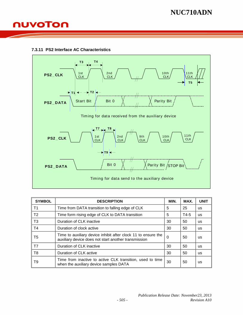
NUC710ADN
Publication Release Date: November23, 2013 - 505 - Revision A10
7.3.11 PS2 Interface AC Characteristics
PS2_CLK
PS2_DATA
T1 T2
T3 T4
Start Bit Bit 0 Parity Bit
STOP Bit
1st CLK
2nd CLK
10th CLK
11th CLK
Timing for data received from the auxiliary device
T9
T8T7
1st CLK
2nd CLK
9th CLK
10th CLK
11th CLK
PS2_DATA
PS2_CLK
Parity Bit
Timing for data send to the auxiliary device
T5
Bit 0
SYMBOL DESCRIPTION MIN. MAX. UNIT
T1 Time from DATA transition to falling edge of CLK 5 25 us
T2 Time form rising edge of CLK to DATA transition 5 T4-5 us
T3 Duration of CLK inactive 30 50 us
T4 Duration of clock active 30 50 us
T5 Time to auxiliary device inhibit after clock 11 to ensure the auxiliary device does not start another transmission 0 50 us
T7 Duration of CLK inactive 30 50 us
T8 Duration of CLK active 30 50 us
T9 Time from inactive to active CLK transition, used to time when the auxiliary device samples DATA 30 50 us

NUC710ADN
Publication Release Date: November235, 2013 - 506 - Revision A10
8. ORDERING INFORMATION PART NUMBER NAME PACKAGE DESCRIPTION
NUC710ADN LQFP176 176 Leads, body 22 x 22 x 1.4 mm, Lead free package

NUC710ADN
Publication Release Date: November23, 2013 - 507 - Revision A10
9. PACKAGE SPECIFICATIONS 176L LQFP (20X20X1.4 mm footprint 2.0mm)
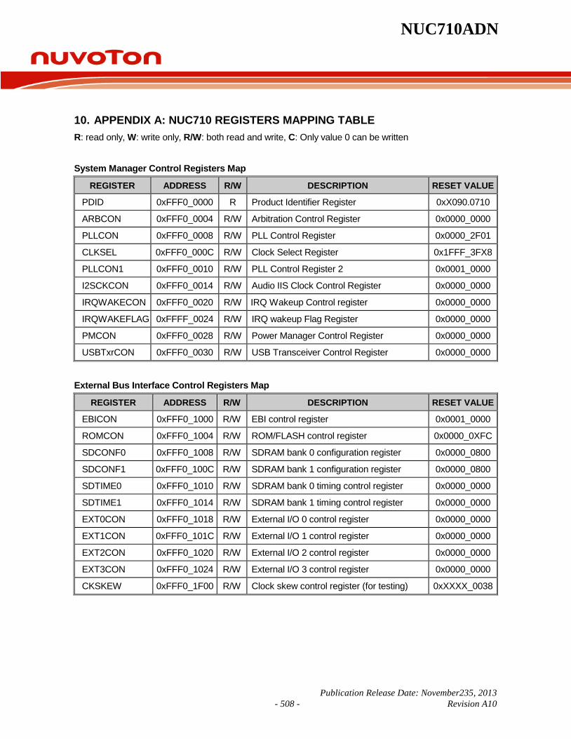
NUC710ADN
Publication Release Date: November235, 2013 - 508 - Revision A10
10. APPENDIX A: NUC710 REGISTERS MAPPING TABLE R: read only, W: write only, R/W: both read and write, C: Only value 0 can be written
System Manager Control Registers Map
REGISTER ADDRESS R/W DESCRIPTION RESET VALUE
PDID 0xFFF0_0000 R Product Identifier Register 0xX090.0710
ARBCON 0xFFF0_0004 R/W Arbitration Control Register 0x0000_0000
PLLCON 0xFFF0_0008 R/W PLL Control Register 0x0000_2F01
CLKSEL 0xFFF0_000C R/W Clock Select Register 0x1FFF_3FX8
PLLCON1 0xFFF0_0010 R/W PLL Control Register 2 0x0001_0000
I2SCKCON 0xFFF0_0014 R/W Audio IIS Clock Control Register 0x0000_0000
IRQWAKECON 0xFFF0_0020 R/W IRQ Wakeup Control register 0x0000_0000
IRQWAKEFLAG 0xFFFF_0024 R/W IRQ wakeup Flag Register 0x0000_0000
PMCON 0xFFF0_0028 R/W Power Manager Control Register 0x0000_0000
USBTxrCON 0xFFF0_0030 R/W USB Transceiver Control Register 0x0000_0000
External Bus Interface Control Registers Map
REGISTER ADDRESS R/W DESCRIPTION RESET VALUE
EBICON 0xFFF0_1000 R/W EBI control register 0x0001_0000
ROMCON 0xFFF0_1004 R/W ROM/FLASH control register 0x0000_0XFC
SDCONF0 0xFFF0_1008 R/W SDRAM bank 0 configuration register 0x0000_0800
SDCONF1 0xFFF0_100C R/W SDRAM bank 1 configuration register 0x0000_0800
SDTIME0 0xFFF0_1010 R/W SDRAM bank 0 timing control register 0x0000_0000
SDTIME1 0xFFF0_1014 R/W SDRAM bank 1 timing control register 0x0000_0000
EXT0CON 0xFFF0_1018 R/W External I/O 0 control register 0x0000_0000
EXT1CON 0xFFF0_101C R/W External I/O 1 control register 0x0000_0000
EXT2CON 0xFFF0_1020 R/W External I/O 2 control register 0x0000_0000
EXT3CON 0xFFF0_1024 R/W External I/O 3 control register 0x0000_0000
CKSKEW 0xFFF0_1F00 R/W Clock skew control register (for testing) 0xXXXX_0038

NUC710ADN
Publication Release Date: November23, 2013 - 509 - Revision A10
Cache Control Registers Map
REGISTER ADDRESS R/W DESCRIPTION RESET VALUE
CAHCNF 0xFFF0_2000 R/W Cache configuration register 0x0000_0000
CAHCON 0xFFF0_2004 R/W Cache control register 0x0000_0000
CAHADR 0xFFF0_2008 R/W Cache address register 0x0000_0000 EMC Registers Map
REGISTER ADDRESS R/W DESCRIPTION RESET VALUE
CAMCMR 0xFFF0_3000 R/W CAM Command Register 0x0000_0000
CAMEN 0xFFF0_3004 R/W CAM Enable Register 0x0000_0000
CAM0M 0xFFF0_3008 R/W CAM0 Most Significant Word Register 0x0000_0000
CAM0L 0xFFF0_300C R/W CAM0 Least Significant Word Register 0x0000_0000
CAM1M 0xFFF0_3010 R/W CAM1 Most Significant Word Register 0x0000_0000
CAM1L 0xFFF0_3014 R/W CAM1 Least Significant Word Register 0x0000_0000
CAM2M 0xFFF0_3018 R/W CAM2 Most Significant Word Register 0x0000_0000
CAM2L 0xFFF0_301C R/W CAM2 Least Significant Word Register 0x0000_0000
CAM3M 0xFFF0_3020 R/W CAM3 Most Significant Word Register 0x0000_0000
CAM3L 0xFFF0_3024 R/W CAM3 Least Significant Word Register 0x0000_0000
CAM4M 0xFFF0_3028 R/W CAM4 Most Significant Word Register 0x0000_0000
CAM4L 0xFFF0_302C R/W CAM4 Least Significant Word Register 0x0000_0000
CAM5M 0xFFF0_3030 R/W CAM5 Most Significant Word Register 0x0000_0000
CAM5L 0xFFF0_3034 R/W CAM5 Least Significant Word Register 0x0000_0000
CAM6M 0xFFF0_3038 R/W CAM6 Most Significant Word Register 0x0000_0000
CAM6L 0xFFF0_303C R/W CAM6 Least Significant Word Register 0x0000_0000
CAM7M 0xFFF0_3040 R/W CAM7 Most Significant Word Register 0x0000_0000
CAM7L 0xFFF0_3044 R/W CAM7 Least Significant Word Register 0x0000_0000
CAM8M 0xFFF0_3048 R/W CAM8 Most Significant Word Register 0x0000_0000
CAM8L 0xFFF0_304C R/W CAM8 Least Significant Word Register 0x0000_0000
CAM9M 0xFFF0_3050 R/W CAM9 Most Significant Word Register 0x0000_0000
CAM9L 0xFFF0_3054 R/W CAM9 Least Significant Word Register 0x0000_0000
CAM10M 0xFFF0_3058 R/W CAM10 Most Significant Word Register 0x0000_0000
CAM10L 0xFFF0_305C R/W CAM10 Least Significant Word Register 0x0000_0000
CAM11M 0xFFF0_3060 R/W CAM11 Most Significant Word Register 0x0000_0000
CAM11L 0xFFF0_3064 R/W CAM11 Least Significant Word Register 0x0000_0000

NUC710ADN
Publication Release Date: November235, 2013 - 510 - Revision A10
EMC Registers Map, continued
REGISTER ADDRESS R/W DESCRIPTION RESET VALUE
CAM12M 0xFFF0_3068 R/W CAM12 Most Significant Word Register 0x0000_0000
CAM12L 0xFFF0_306C R/W CAM12 Least Significant Word Register 0x0000_0000
CAM13M 0xFFF0_3070 R/W CAM13 Most Significant Word Register 0x0000_0000
CAM13L 0xFFF0_3074 R/W CAM13 Least Significant Word Register 0x0000_0000
CAM14M 0xFFF0_3078 R/W CAM14 Most Significant Word Register 0x0000_0000
CAM14L 0xFFF0_307C R/W CAM14 Least Significant Word Register 0x0000_0000
CAM15M 0xFFF0_3080 R/W CAM15 Most Significant Word Register 0x0000_0000
CAM15L 0xFFF0_3084 R/W CAM15 Least Significant Word Register 0x0000_0000
TXDLSA 0xFFF0_3088 R/W Transmit Descriptor Link List Start Address Register 0xFFFF_FFFC
RXDLSA 0xFFF0_308C R/W Receive Descriptor Link List Start Address Register 0xFFFF_FFFC
MCMDR 0xFFF0_3090 R/W MAC Command Register 0x0000_0000
MIID 0xFFF0_3094 R/W MII Management Data Register 0x0000_0000
MIIDA 0xFFF0_3098 R/W MII Management Control and Address Register 0x0090_0000
FFTCR 0xFFF0_309C R/W FIFO Threshold Control Register 0x0000_0101
TSDR 0xFFF0_30A0 W Transmit Start Demand Register Undefined
RSDR 0xFFF0_30A4 W Receive Start Demand Register Undefined
DMARFC 0xFFF0_30A8 R/W Maximum Receive Frame Control Register 0x0000_0800
MIEN 0xFFF0_30AC R/W MAC Interrupt Enable Register 0x0000_0000
MISTA 0xFFF0_30B0 R/W MAC Interrupt Status Register 0x0000_0000
MGSTA 0xFFF0_30B4 R/W MAC General Status Register 0x0000_0000
MPCNT 0xFFF0_30B8 R/W Missed Packet Count Register 0x0000_7FFF
MRPC 0xFFF0_30BC R MAC Receive Pause Count Register 0x0000_0000
MRPCC 0xFFF0_30C0 R MAC Receive Pause Current Count Register 0x0000_0000
MREPC 0xFFF0_30C4 R MAC Remote Pause Count Register 0x0000_0000
DMARFS 0xFFF0_30C8 R/W DMA Receive Frame Status Register 0x0000_0000
CTXDSA 0xFFF0_30CC R Current Transmit Descriptor Start Address Register 0x0000_0000
CTXBSA 0xFFF0_30D0 R Current Transmit Buffer Start Address Register 0x0000_0000
CRXDSA 0xFFF0_30D4 R Current Receive Descriptor Start Address Register 0x0000_0000
CRXBSA 0xFFF0_30D8 R Current Receive Buffer Start Address Register 0x0000_0000
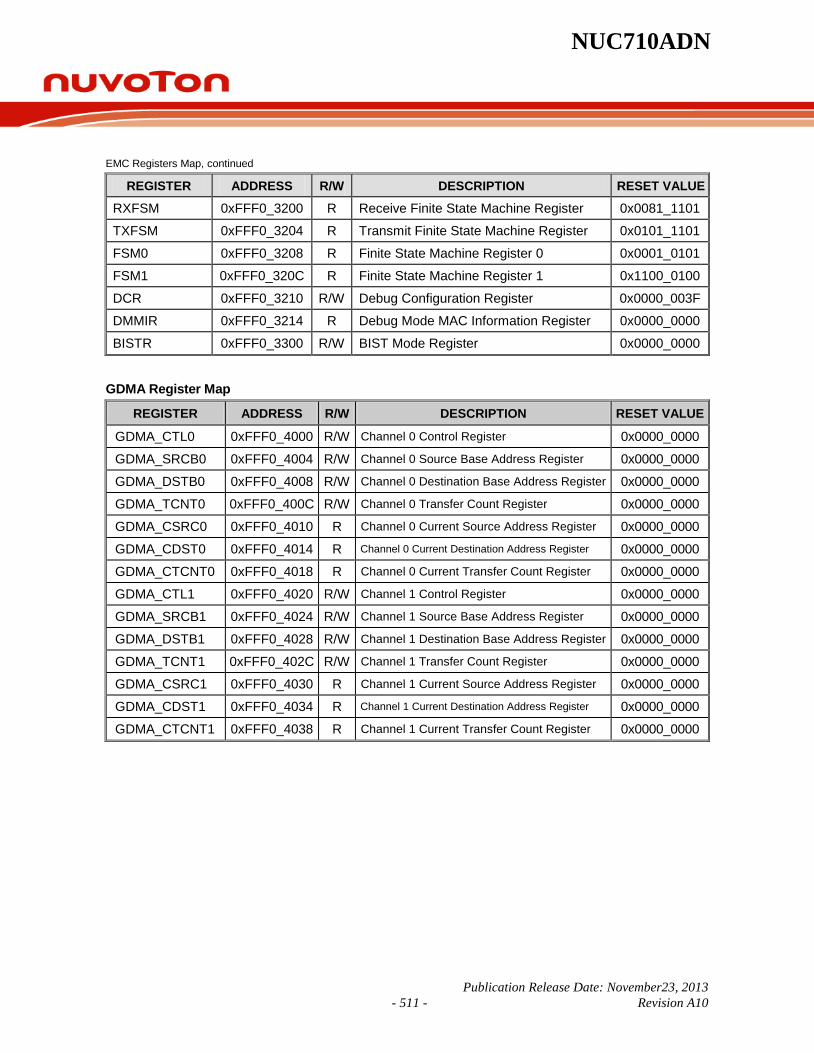
NUC710ADN
Publication Release Date: November23, 2013 - 511 - Revision A10
EMC Registers Map, continued
REGISTER ADDRESS R/W DESCRIPTION RESET VALUE
RXFSM 0xFFF0_3200 R Receive Finite State Machine Register 0x0081_1101
TXFSM 0xFFF0_3204 R Transmit Finite State Machine Register 0x0101_1101
FSM0 0xFFF0_3208 R Finite State Machine Register 0 0x0001_0101
FSM1 0xFFF0_320C R Finite State Machine Register 1 0x1100_0100
DCR 0xFFF0_3210 R/W Debug Configuration Register 0x0000_003F
DMMIR 0xFFF0_3214 R Debug Mode MAC Information Register 0x0000_0000
BISTR 0xFFF0_3300 R/W BIST Mode Register 0x0000_0000
GDMA Register Map
REGISTER ADDRESS R/W DESCRIPTION RESET VALUE
GDMA_CTL0 0xFFF0_4000 R/W Channel 0 Control Register 0x0000_0000
GDMA_SRCB0 0xFFF0_4004 R/W Channel 0 Source Base Address Register 0x0000_0000
GDMA_DSTB0 0xFFF0_4008 R/W Channel 0 Destination Base Address Register 0x0000_0000
GDMA_TCNT0 0xFFF0_400C R/W Channel 0 Transfer Count Register 0x0000_0000
GDMA_CSRC0 0xFFF0_4010 R Channel 0 Current Source Address Register 0x0000_0000
GDMA_CDST0 0xFFF0_4014 R Channel 0 Current Destination Address Register 0x0000_0000
GDMA_CTCNT0 0xFFF0_4018 R Channel 0 Current Transfer Count Register 0x0000_0000
GDMA_CTL1 0xFFF0_4020 R/W Channel 1 Control Register 0x0000_0000
GDMA_SRCB1 0xFFF0_4024 R/W Channel 1 Source Base Address Register 0x0000_0000
GDMA_DSTB1 0xFFF0_4028 R/W Channel 1 Destination Base Address Register 0x0000_0000
GDMA_TCNT1 0xFFF0_402C R/W Channel 1 Transfer Count Register 0x0000_0000
GDMA_CSRC1 0xFFF0_4030 R Channel 1 Current Source Address Register 0x0000_0000
GDMA_CDST1 0xFFF0_4034 R Channel 1 Current Destination Address Register 0x0000_0000
GDMA_CTCNT1 0xFFF0_4038 R Channel 1 Current Transfer Count Register 0x0000_0000

NUC710ADN
Publication Release Date: November235, 2013 - 512 - Revision A10
USB Host Controller Register Map
REGISTER ADDRESS R/W DESCRIPTION RESET VALUE
OpenHCI Registers HcRevision 0xFFF0_5000 R Host Controller Revision Register 0x0000_0010
HcControl 0xFFF0_5004 R/W Host Controller Control Register 0x0000_0000
HcCommandStatus 0xFFF0_5008 R/W Host Controller Command Status Register 0x0000_0000
HcInterruptStatus 0xFFF0_500C R/W Host Controller Interrupt Status Register 0x0000_0000
HcInterruptEnbale 0xFFF0_5010 R/W Host Controller Interrupt Enable Register 0x0000_0000
HcInterruptDisbale 0xFFF0_5014 R/W Host Controller Interrupt Disable Register 0x0000_0000
HcHCCA 0xFFF0_5018 R/W Host Controller Communication Area Register 0x0000_0000
HcPeriodCurrentED 0xFFF0_501C R/W Host Controller Period Current ED Register 0x0000_0000
HcControlHeadED 0xFFF0_5020 R/W Host Controller Control Head ED Register 0x0000_0000
HcControlCurrentED 0xFFF0_5024 R/W Host Controller Control Current ED Register 0x0000_0000
HcBulkHeadEd 0xFFF0_5028 R/W Host Controller Bulk Head ED Register 0x0000_0000
HcBulkCurrentED 0xFFF0_502C R/W Host Controller Bulk Current ED Register 0x0000_0000
HcDoneHeadED 0xFFF0_5030 R/W Host Controller Done Head Register 0x0000_0000
HcFmInterval 0xFFF0_5034 R/W Host Controller Frame Interval Register 0x0000_2EDF
HcFrameRemaining 0xFFF0_5038 R Host Controller Frame Remaining Register 0x0000_0000
HcFmNumber 0xFFF0_503C R Host Controller Frame Number Register 0x0000_0000
HcPeriodicStart 0xFFF0_5040 R/W Host Controller Periodic Start Register 0x0000_0000
HcLSThreshold 0xFFF0_5044 R/W Host Controller Low Speed Threshold Register 0x0000_0628
HcRhDescriptorA 0xFFF0_5048 R/W Host Controller Root Hub Descriptor A Register 0x0100_0002
HcRhDescriptorB 0xFFF0_504C R/W Host Controller Root Hub Descriptor B Register 0x0000_0000
HcRhStatus 0xFFF0_5050 R/W Host Controller Root Hub Status Register 0x0000_0000
HcRhPortStatus [1] 0xFFF0_5054 R/W Host Controller Root Hub Port Status [1] 0x0000_0000
HcRhPortStatus [2] 0xFFF0_5058 R/W Host Controller Root Hub Port Status [2] 0x0000_0000
USB Configuration Registers TestModeEnable 0xFFF0_5200 R/W USB Test Mode Enable Register 0x0XXX_XXXX OperationalModeEnable 0xFFF0_5204 R/W USB Operational Mode Enable Register 0x0000_0000

NUC710ADN
Publication Release Date: November23, 2013 - 513 - Revision A10
USB Device Register Map
REGISTER ADDRESS R/W DESCRIPTION RESET VALUE
USB_CTL 0xFFF0_6000 R/W USB control register 0x0000_0000
VCMD 0xFFF0_6004 R/W USB class or vendor command register 0x0000_0000
USB_IE 0xFFF0_6008 R/W USB interrupt enable register 0x0000_0000
USB_IS 0xFFF0_600C R USB interrupt status register 0x0000_0000
USB_IC 0xFFF0_6010 R/W USB interrupt status clear register 0x0000_0000
USB_IFSTR 0xFFF0_6014 R/W USB interface and string register 0x0000_0000
USB_ODATA0 0xFFF0_6018 R USB control transfer-out port 0 register 0x0000_0000
USB_ODATA1 0xFFF0_601C R USB control transfer-out port 1 register 0x0000_0000
USB_ODATA2 0xFFF0_6020 R USB control transfer-out port 2 register 0x0000_0000
USB_ODATA3 0xFFF0_6024 R USB control transfer-out port 3 register 0x0000_0000
USB_IDATA0 0xFFF0_6028 R/W USB transfer-in data port0 register 0x0000_0000
USB_IDATA1 0xFFF0_602C R/W USB control transfer-in data port 1 0x0000_0000
USB_IDATA2 0xFFF0_6030 R/W USB control transfer-in data port 2 0x0000_0000
USB_IDATA3 0xFFF0_6034 R/W USB control transfer-in data port 3 0x0000_0000
USB_SIE 0xFFF0_6038 R USB SIE status Register 0x0000_0000
USB_ENG 0xFFF0_603C R/W USB Engine Register 0x0000_0000
USB_CTLS 0xFFF0_6040 R USB control transfer status register 0x0000_0000
USB_CONFD 0xFFF0_6044 R/W USB Configured Value register 0x0000_0000
EPA_INFO 0xFFF0_6048 R/W USB endpoint A information register 0x0000_0000
EPA_CTL 0xFFF0_604C R/W USB endpoint A control register 0x0000_0000
EPA_IE 0xFFF0_6050 R/W USB endpoint A Interrupt Enable register 0x0000_0000
EPA_IC 0xFFF0_6054 W USB endpoint A interrupt clear register 0x0000_0000
EPA_IS 0xFFF0_6058 R USB endpoint A interrupt status register 0x0000_0000
EPA_ADDR 0xFFF0_605C R/W USB endpoint A address register 0x0000_0000
EPA_LENTH 0xFFF0_6060 R/W USB endpoint A transfer length register 0x0000_0000
EPB_INFO 0xFFF0_6064 R/W USB endpoint B information register 0x0000_0000
EPB_CTL 0xFFF0_6068 R/W USB endpoint B control register 0x0000_0000
EPB_IE 0xFFF0_606C R/W USB endpoint B Interrupt Enable register 0x0000_0000
EPB_IC 0xFFF0_6070 W USB endpoint B interrupt clear register 0x0000_0000
EPB_IS 0xFFF0_6074 R USB endpoint B interrupt status register 0x0000_0000
EPB_ADDR 0xFFF0_6078 R/W USB endpoint B address register 0x0000_0000

NUC710ADN
Publication Release Date: November235, 2013 - 514 - Revision A10
USB Device Register Map continued
REGISTER ADDRESS R/W DESCRIPTION RESET VALUE
EPB_LENTH 0xFFF0_607C R/W USB endpoint B transfer length register 0x0000_0000
EPC_INFO 0xFFF0_6080 R/W USB endpoint C information register 0x0000_0000
EPC_CTL 0xFFF0_6084 R/W USB endpoint C control register 0x0000_0000
EPC_IE 0xFFF0_6 088 R/W USB endpoint C Interrupt Enable register 0x0000_0000
EPC_IC 0xFFF0_608C W USB endpoint C interrupt clear register 0x0000_0000
EPC_IS 0xFFF0_6090 R USB endpoint C interrupt status register 0x0000_0000
EPC_ADDR 0xFFF0_6094 R/W USB endpoint C address register 0x0000_0000
EPC_LENTH 0xFFF0_6098 R/W USB endpoint C transfer length register 0x0000_0000
EPA_XFER 0xFFF0_609C R/W USB endpoint A remain transfer length register 0x0000_0000
EPA_PKT 0xFFF0_60A0 R/W USB endpoint A remain packet length register 0x0000_0000
EPB_XFER 0xFFF0_60A4 R/W USB endpoint B remain transfer length register 0x0000_0000
EPB_PKT 0xFFF0_60A8 R/W USB endpoint B remain packet length register 0x0000_0000
EPC_XFER 0xFFF0_60AC R/W USB endpoint C remain transfer length register 0x0000_0000
EPC_PKT 0xFFF0_60B0 R/W USB endpoint C remain packet length register 0x0000_0000
SD Control Register Map
REGISTER ADDRESS R/W DESCRIPTION RESET VALUE
SDGCR 0xFFF0_7000 R/W SD Global Control Register 0x0000_0000
SDDSA 0xFFF0_7004 R/W SD DMA Transfer Starting Address Register 0x0000_0000
SDBCR 0xFFF0_7008 R/W SD DMA Byte Count Register 0x0000_0000
SDGIER 0xFFF0_700C R/W SD Global Interrupt Enable Register 0x0000_0000
SDGISR 0xFFF0_7010 R/W SD Global Interrupt Status Register 0x0000_0000
SDBIST 0xFFF0_7014 R/W SD BIST Register 0x0000_0000
SDCR 0xFFF0_7300 R/W SD Control Register 0x0000_0000
SDHINI 0xFFF0_7304 R/W SD Host Initial Register 0x0000_0018
SDIER 0xFFF0_7308 R/W SD Interrupt Enable Register 0x0000_0000
SDISR 0xFFF0_730C R/W SD Interrupt Status Register 0x0000_00XX
SDAUG 0xFFF0_7310 R/W SD Command Argument Register 0x0000_0000
SDRSP0 0xFFF0_7314 R SD Receive Response Token Register 0 0xXXXX_XXXX
SDRSP1 0xFFF0_7318 R SD Receive Response Token Register 1 0x0000_XXXX
SDBLEN 0xFFF0_731C R/W SD Block Length Register 0x0000_0000
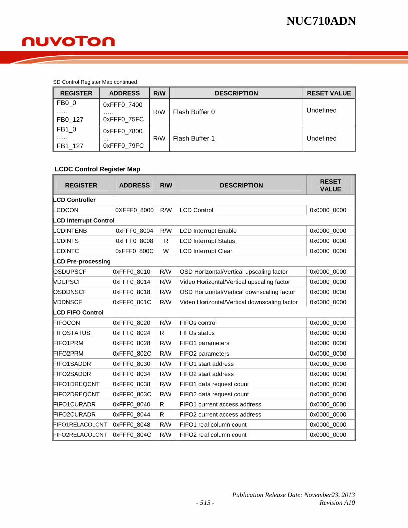
NUC710ADN
Publication Release Date: November23, 2013 - 515 - Revision A10
SD Control Register Map continued
REGISTER ADDRESS R/W DESCRIPTION RESET VALUE FB0_0 ….. FB0_127
0xFFF0_7400 ….. 0xFFF0_75FC
R/W Flash Buffer 0 Undefined
FB1_0 ….. FB1_127
0xFFF0_7800 ... 0xFFF0_79FC
R/W Flash Buffer 1 Undefined
LCDC Control Register Map
REGISTER ADDRESS R/W DESCRIPTION RESET VALUE
LCD Controller LCDCON 0XFFF0_8000 R/W LCD Control 0x0000_0000
LCD Interrupt Control LCDINTENB 0xFFF0_8004 R/W LCD Interrupt Enable 0x0000_0000
LCDINTS 0xFFF0_8008 R LCD Interrupt Status 0x0000_0000
LCDINTC 0xFFF0_800C W LCD Interrupt Clear 0x0000_0000
LCD Pre-processing
OSDUPSCF 0xFFF0_8010 R/W OSD Horizontal/Vertical upscaling factor 0x0000_0000
VDUPSCF 0xFFF0_8014 R/W Video Horizontal/Vertical upscaling factor 0x0000_0000
OSDDNSCF 0xFFF0_8018 R/W OSD Horizontal/Vertical downscaling factor 0x0000_0000
VDDNSCF 0xFFF0_801C R/W Video Horizontal/Vertical downscaling factor 0x0000_0000
LCD FIFO Control FIFOCON 0xFFF0_8020 R/W FIFOs control 0x0000_0000
FIFOSTATUS 0xFFF0_8024 R FIFOs status 0x0000_0000
FIFO1PRM 0xFFF0_8028 R/W FIFO1 parameters 0x0000_0000
FIFO2PRM 0xFFF0_802C R/W FIFO2 parameters 0x0000_0000
FIFO1SADDR 0xFFF0_8030 R/W FIFO1 start address 0x0000_0000
FIFO2SADDR 0xFFF0_8034 R/W FIFO2 start address 0x0000_0000
FIFO1DREQCNT 0xFFF0_8038 R/W FIFO1 data request count 0x0000_0000
FIFO2DREQCNT 0xFFF0_803C R/W FIFO2 data request count 0x0000_0000
FIFO1CURADR 0xFFF0_8040 R FIFO1 current access address 0x0000_0000
FIFO2CURADR 0xFFF0_8044 R FIFO2 current access address 0x0000_0000
FIFO1RELACOLCNT 0xFFF0_8048 R/W FIFO1 real column count 0x0000_0000
FIFO2RELACOLCNT 0xFFF0_804C R/W FIFO2 real column count 0x0000_0000

NUC710ADN
Publication Release Date: November235, 2013 - 516 - Revision A10
LCDC Control Register Map continued.
REGISTER ADDRESS R/W DESCRIPTION RESET VALUE Color Generation
VDLUTENTRY1 0xFFF0_8050 R/W Video lookup table entry index 1 0x0000_0000
VDLUTENTRY2 0xFFF0_8054 R/W Video lookup table entry index 2 0x0000_0000
VDLUTENTRY3 0xFFF0_8058 R/W Video lookup table entry index 3 0x0000_0000
VDLUTENTRY4 0xFFF0_805C R/W Video lookup table entry index 4 0x0000_0000
OSDLUTENTRY1 0xFFF0_8060 R/W OSD lookup table entry index 1 0x0000_0000
OSDLUTENTRY2 0xFFF0_8064 R/W OSD lookup table entry index 2 0x0000_0000
OSDLUTENTRY3 0xFFF0_8068 R/W OSD lookup table entry index 3 0x0000_0000
OSDLUTENTRY4 0xFFF0_806C R/W OSD lookup table entry index 4 0x0000_0000
DITHP1 0xFFF0_8070 R/W Gray level dithered data duty pattern 1 0x0101_0001
DITHP2 0xFFF0_8074 R/W Gray level dithered data duty pattern 2 0x1111_0841
DITHP3 0xFFF0_8078 R/W Gray level dithered data duty pattern 3 0x4949_2491
DITHP4 0xFFF0_807C R/W Gray level dithered data duty pattern 4 0x5555_52A5
DITHP5 0xFFF0_8080 R/W Gray level dithered data duty pattern 5 0xB6B6_B556
DITHP6 0xFFF0_8084 R/W Gray level dithered data duty pattern 6 0xEEEE_DB6E
DITHP7 0xFFF0_8088 R/W Gray level dithered data duty pattern 7 0xEFEF_EFBE
LCD Post-processing
DDISPCP 0xFFF0_8090 R/W Dummy Display Color Pattern 0x0000_0000
VWINS 0xFFF0_8094 R/W Video Window Starting Coordinate 0x0000_0000
VWINE 0xFFF0_8098 R/W Video Window Ending Coordinate 0x0000_0000
OSDWINS 0xFFF0_809C R/W OSD Window Starting Coordinate 0x0000_0000
OSDWINE 0xFFF0_80A0 R/W OSD Window Ending Coordinate 0x0000_0000
OSDOVCN 0xFFF0_80A4 R/W OSD Overlay Control 0x0000_0000
OSDCKP 0xFFF0_80A8 R/W OSD Overlay Color-Key Pattern 0x0000_0000
OSDCKM 0xFFF0_80AC R/W OSD Overlay Color-Key Mask 0x0000_0000
LCD Timing Generation
LCDTCON1 0xFFF0_80B0 R/W LCD Timing Control 1 0x0000_0000
LCDTCON2 0xFFF0_80B4 R/W LCD Timing Control 2 0x0000_0000
LCDTCON3 0xFFF0_80B8 R/W LCD Timing Control 3 0x0000_0000
LCDTCON4 0xFFF0_80BC R/W LCD Timing Control 4 0x0000_0000
LCDTCON5 0xFFF0_80C0 R/W LCD Timing Control 5 0x0000_0000
LCDTCON6 0xFFF0_80C4 R LCD Timing Control 6 0x0000_0000
Lookup Table SRAM Build In Self Test BIST 0xFFF0_80D0 R/W 0x0000_0000

NUC710ADN
Publication Release Date: November23, 2013 - 517 - Revision A10
LCDC Control Register Map, continued.
REGISTER ADDRESS R/W DESCRIPTION RESET VALUE Lookup Table SRAM
0xFFF0_0100 … 0xFFF0_84FF
R/W Look-Up Table RAM 0xXXXX_XXXX
Audio Control Register Map
REGISTER ADDRESS R/W DESCRIPTION RESET VALUE
ACTL_CON 0xFFF0_9000 R/W Audio controller control register 0x0000_0000 ACTL_RESET 0xFFF0_9004 R/W Sub block reset control register 0x0000_0000
ACTL_RDSTB 0xFFF0_9008 R/W DMA destination base address register for record 0x0000_0000
ACTL_RDST_LENGTH 0xFFF0_900C R/W DMA destination length register for record 0x0000_0000
ACTL_RDSTC 0xFFF0_9010 R DMA destination current address register for record 0x0000_0000
ACTL_RSR 0xFFF0_9014 R/W Record status register 0x0000_0000
ACTL_PDSTB 0xFFF0_9018 R/W DMA destination base address register for play 0x0000_0000
ACTL_PDST_LENGTH 0xFFF0_901C R/W DMA destination length register for play 0x0000_0000
ACTL_PDSTC 0xFFF0_9020 R DMA destination current address register for play 0x0000_0000
ACTL_PSR 0xFFF0_9024 R/W Play status register 0x0000_0004 ACTL_IISCON 0xFFF0_9028 R/W IIS control register 0x0000_0000 ACTL_ACCON 0xFFF0_902C R/W AC-link control register 0x0000_0000 ACTL_ACOS0 0xFFF0_9030 R/W AC-link out slot 0 0x0000_0000 ACTL_ACOS1 0xFFF0_9034 R/W AC-link out slot 1 0x0000_0080 ACTL_ACOS2 0xFFF0_9038 R/W AC-link out slot 2 0x0000_0000 ACTL_ACIS0 0xFFF0_903C R AC-link in slot 0 0x0000_0000 ACTL_ACIS1 0xFFF0_9040 R AC-link in slot 1 0x0000_0000 ACTL_ACIS2 0xFFF0_9044 R AC-link in slot 2 0x0000_0000 Cache Controller Test Registers Map
REGISTER ADDRESS R/W DESCRIPTION RESET VALUE CTEST0 0xFFF6_0000 R/W Cache test register 0 0x0000_0000 CTEST1 0xFFF6_0004 R Cache test register 1 0x0000_0000

NUC710ADN
Publication Release Date: November235, 2013 - 518 - Revision A10
UART0 Control Registers Map
REGISTER ADDRESS R/W DESCRIPTION RESET VALUE
UART0_RBR 0xFFF8_0000 R Receive Buffer Register (DLAB = 0) Undefined
UART0_THR 0xFFF8_0000 W Transmit Holding Register (DLAB = 0) Undefined
UART0_IER 0xFFF8_0004 R/W Interrupt Enable Register (DLAB = 0) 0x0000_0000
UART0_DLL 0xFFF8_0000 R/W Divisor Latch Register (LS) (DLAB = 1)
0x0000_0000
UART0_DLM 0xFFF8_0004 R/W Divisor Latch Register (MS) (DLAB = 1)
0x0000_0000
UART0_IIR 0xFFF8_0008 R Interrupt Identification Register 0x8181_8181
UART0_FCR 0xFFF8_0008 W FIFO Control Register Undefined
UART0_LCR 0xFFF8_000C R/W Line Control Register 0x0000_0000
UART0_LSR 0xFFF8_0014 R Line Status Register 0x6060_6060
UART0_TOR 0xFFF8_001C R Timeout Register 0x0000_0000
High Speed UART1 Control Registers Map
REGISTER ADDRESS R/W DESCRIPTION RESET VALUE
UART1_RBR 0xFFF8_0100 R Receive Buffer Register (DLAB = 0) Undefined
UART1_THR 0xFFF8_0100 W Transmit Holding Register (DLAB = 0) Undefined
UART1_IER 0xFFF8_0104 R/W Interrupt Enable Register (DLAB = 0) 0x0000_0000
UART1_DLL 0xFFF8_0100 R/W Divisor Latch Register (LS) (DLAB = 1) 0x0000_0000
UART1_DLM 0xFFF8_0104 R/W Divisor Latch Register (MS) (DLAB = 1) 0x0000_0000
UART1_IIR 0xFFF8_0108 R Interrupt Identification Register 0x8181_8181
UART1_FCR 0xFFF8_0108 W FIFO Control Register Undefined
UART1_LCR 0xFFF8_010C R/W Line Control Register 0x0000_0000
UART1_MCR 0xFFF8_0110 R/W Modem Control Register 0x0000_0000
UART1_LSR 0xFFF8_0114 R Line Status Register 0x6060.6060
UART1_MSR 0xFFF8_0118 R MODEM Status Register 0x0000_0000
UART1_TOR 0xFFF8_011C R Timeout Register 0x0000_0000
UART1_UBCR 0xFFF8_0120 R/W UART1 Bluetooth Control Register 0x0000_0000

NUC710ADN
Publication Release Date: November23, 2013 - 519 - Revision A10
UART2 Control Register Map
REGISTER ADDRESS R/W DESCRIPTION RESET VALUE
UART2_RBR 0xFFF8_0200 R Receive Buffer Register (DLAB = 0) Undefined
UART2_THR 0xFFF8_0200 W Transmit Holding Register (DLAB = 0) Undefined
UART2_IER 0xFFF8_0204 R/W Interrupt Enable Register (DLAB = 0) 0x0000_0000
UART2_DLL 0xFFF8_0200 R/W Divisor Latch Register (LS) (DLAB = 1) 0x0000_0000
UART2_DLM 0xFFF8_0204 R/W Divisor Latch Register (MS) (DLAB = 1) 0x0000_0000
UART2_IIR 0xFFF8_0208 R Interrupt Identification Register 0x8181_8181
UART2_FCR 0xFFF8_0208 W FIFO Control Register Undefined
UART2_LCR 0xFFF8_020C R/W Line Control Register 0x0000_0000
UART2_MCR 0xFFF8_0210 R/W Modem Control Register 0x0000_0000
UART2_LSR 0xFFF8_0214 R Line Status Register 0x6060_6060
UART2_MSR 0xFFF8_0218 R MODEM Status Register 0x0000_0000
UART2_TOR 0xFFF8_021C R Timeout Register 0x0000_0000
UART2_IRCR 0xFFF8_0220 R/W IrDA Control Register 0x0000_0040
UART3 Control Register Map
REGISTER ADDRESS R/W DESCRIPTION RESET VALUE
UART3_RBR 0xFFF8_0300 R Receive Buffer Register (DLAB = 0) Undefined
UART3_THR 0xFFF8_0300 W Transmit Holding Register (DLAB = 0) Undefined
UART3_IER 0xFFF8_0304 R/W Interrupt Enable Register (DLAB = 0) 0x0000_0000
UART3_DLL 0xFFF8_0300 R/W Divisor Latch Register (LS) (DLAB = 1)
0x0000_0000
UART3_DLM 0xFFF8_0304 R/W Divisor Latch Register (MS) (DLAB = 1)
0x0000_0000
UART3_IIR 0xFFF8_0308 R Interrupt Identification Register 0x8181_8181
UART3_FCR 0xFFF8_0308 W FIFO Control Register Undefined
UART3_LCR 0xFFF8_030C R/W Line Control Register 0x0000_0000
UART3_MCR 0xFFF8_0310 R/W Modem Control Register 0x0000_0000
UART3_LSR 0xFFF8_0314 R Line Status Register 0x6060_6060
UART3_MSR 0xFFF8_0318 R MODEM Status Register 0x0000_0000
UART3_TOR 0xFFF8_031C R Timeout Register 0x0000_0000
Timer Control Registers Map
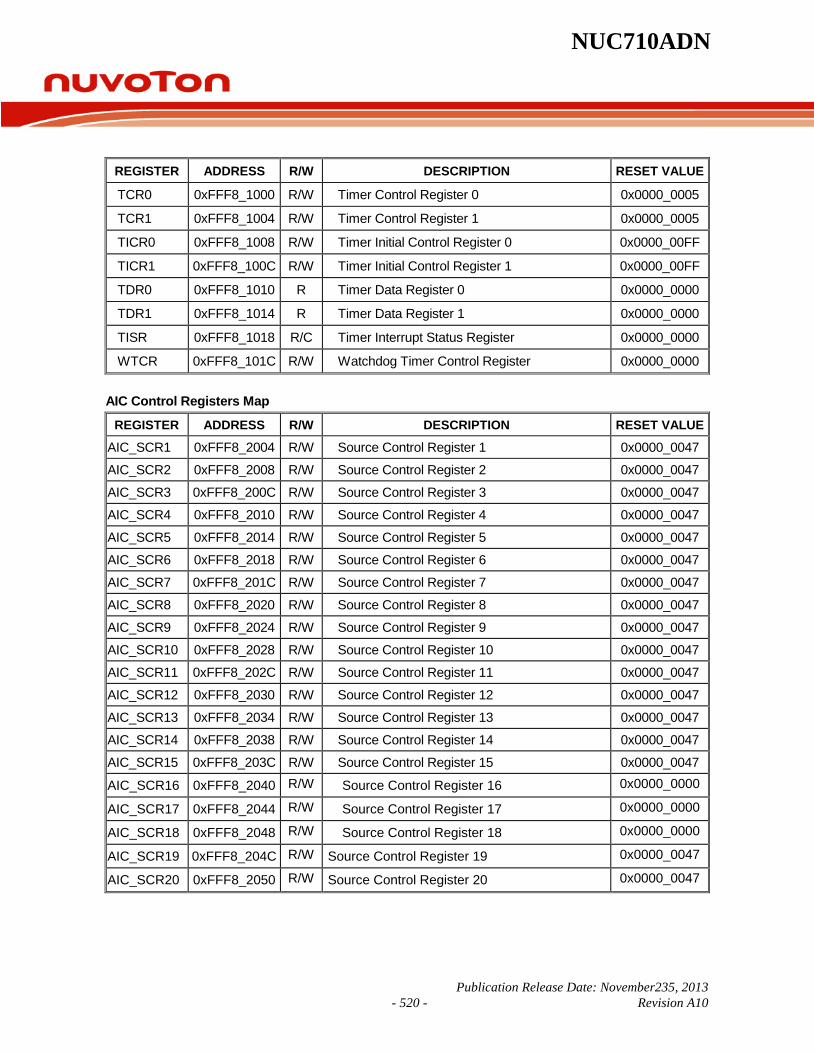
NUC710ADN
Publication Release Date: November235, 2013 - 520 - Revision A10
REGISTER ADDRESS R/W DESCRIPTION RESET VALUE
TCR0 0xFFF8_1000 R/W Timer Control Register 0 0x0000_0005
TCR1 0xFFF8_1004 R/W Timer Control Register 1 0x0000_0005
TICR0 0xFFF8_1008 R/W Timer Initial Control Register 0 0x0000_00FF
TICR1 0xFFF8_100C R/W Timer Initial Control Register 1 0x0000_00FF
TDR0 0xFFF8_1010 R Timer Data Register 0 0x0000_0000
TDR1 0xFFF8_1014 R Timer Data Register 1 0x0000_0000
TISR 0xFFF8_1018 R/C Timer Interrupt Status Register 0x0000_0000
WTCR 0xFFF8_101C R/W Watchdog Timer Control Register 0x0000_0000 AIC Control Registers Map
REGISTER ADDRESS R/W DESCRIPTION RESET VALUE
AIC_SCR1 0xFFF8_2004 R/W Source Control Register 1 0x0000_0047
AIC_SCR2 0xFFF8_2008 R/W Source Control Register 2 0x0000_0047
AIC_SCR3 0xFFF8_200C R/W Source Control Register 3 0x0000_0047
AIC_SCR4 0xFFF8_2010 R/W Source Control Register 4 0x0000_0047
AIC_SCR5 0xFFF8_2014 R/W Source Control Register 5 0x0000_0047
AIC_SCR6 0xFFF8_2018 R/W Source Control Register 6 0x0000_0047
AIC_SCR7 0xFFF8_201C R/W Source Control Register 7 0x0000_0047
AIC_SCR8 0xFFF8_2020 R/W Source Control Register 8 0x0000_0047
AIC_SCR9 0xFFF8_2024 R/W Source Control Register 9 0x0000_0047
AIC_SCR10 0xFFF8_2028 R/W Source Control Register 10 0x0000_0047
AIC_SCR11 0xFFF8_202C R/W Source Control Register 11 0x0000_0047
AIC_SCR12 0xFFF8_2030 R/W Source Control Register 12 0x0000_0047
AIC_SCR13 0xFFF8_2034 R/W Source Control Register 13 0x0000_0047
AIC_SCR14 0xFFF8_2038 R/W Source Control Register 14 0x0000_0047
AIC_SCR15 0xFFF8_203C R/W Source Control Register 15 0x0000_0047
AIC_SCR16 0xFFF8_2040 R/W Source Control Register 16 0x0000_0000
AIC_SCR17 0xFFF8_2044 R/W Source Control Register 17 0x0000_0000
AIC_SCR18 0xFFF8_2048 R/W Source Control Register 18 0x0000_0000
AIC_SCR19 0xFFF8_204C R/W Source Control Register 19 0x0000_0047
AIC_SCR20 0xFFF8_2050 R/W Source Control Register 20 0x0000_0047

NUC710ADN
Publication Release Date: November23, 2013 - 521 - Revision A10
AIC Control Registers Map continued
REGISTER ADDRESS R/W DESCRIPTION RESET VALUE
AIC_SCR21 0xFFF8_2054 R/W Source Control Register 21 0x0000_0047
AIC_SCR22 0xFFF8_2058 R/W Source Control Register 22 0x0000_0047
AIC_SCR23 0xFFF8_205C R/W Source Control Register 23 0x0000_0047
AIC_SCR24 0xFFF8_2060 R/W Source Control Register 24 0x0000_0047
AIC_SCR25 0xFFF8_2064 R/W Source Control Register 25 0x0000_0047
AIC_SCR26 0xFFF8_2068 R/W Source Control Register 26 0x0000_0047
AIC_SCR27 0xFFF8_206C R/W Source Control Register 27 0x0000_0047
AIC_SCR28 0xFFF8_2070 R/W Source Control Register 28 0x0000_0047
AIC_SCR29 0xFFF8_2074 R/W Source Control Register 29 0x0000_0047
AIC_SCR30 0xFFF8_2078 R/W Source Control Register 30 0x0000_0047
AIC_SCR31 0xFFF8_207C R/W Source Control Register 31 0x0000_0047
AIC_IRSR 0xFFF8_2100 R Interrupt Raw Status Register 0x0000_0000
AIC_IASR 0xFFF8_2104 R Interrupt Active Status Register 0x0000_0000
AIC_ISR 0xFFF8_2108 R Interrupt Status Register 0x0000_0000
AIC_IPER 0xFFF8_210C R Interrupt Priority Encoding Register 0x0000_0000
AIC_ISNR 0xFFF8_2110 R Interrupt Source Number Register 0x0000_0000
AIC_IMR 0xFFF8_2114 R Interrupt Mask Register 0x0000_0000
AIC_OISR 0xFFF8_2118 R Output Interrupt Status Register 0x0000_0000
AIC_MECR 0xFFF8_2120 W Mask Enable Command Register Undefined
AIC_MDCR 0xFFF8_2124 W Mask Disable Command Register Undefined
AIC_SSCR 0xFFF8_2128 W Source Set Command Register Undefined
AIC_SCCR 0xFFF8_212C W Source Clear Command Register Undefined AIC_EOSCR 0xFFF8_2130 W End of Service Command Register Undefined
AIC_TEST 0xFFF8_2200 W ICE/Debug mode Register Undefined

NUC710ADN
Publication Release Date: November235, 2013 - 522 - Revision A10
GPIO Control Register Map
REGISTER ADDRESS R/W DESCRIPTION RESET VALUE
GPIO_CFG0 0xFFF8_3000 R/W GPIO port0 configuration register 0x0000_0000
GPIO_DIR0 0xFFF8_3004 R/W GPIO port0 direction control register 0x0000_0000
GPIO_DATAOUT0 0xFFF8_3008 R/W GPIO port0 data output register 0x0000_0000
GPIO_DATAIN0 0xFFF8_300C R GPIO port0 data input register 0xXXXX_XXXX
GPIO_CFG1 0xFFF8_3010 R/W GPIO port1 configuration register 0x0000_0000
GPIO_DIR1 0xFFF8_3014 R/W GPIO port1 direction control register 0x0000_0000
GPIO_DATAOUT1 0xFFF8_3018 R/W GPIO port1 data output register 0x0000_0000
GPIO_DATAIN1 0xFFF8_301C R GPIO port1 data input register 0xXXXX_XXXX
GPIO_CFG2 0xFFF8_3020 R/W GPIO port2 configuration register 0x0000_0000
GPIO_DIR2 0xFFF8_3024 R/W GPIO port2 direction control register 0x0000_0000
GPIO_DATAOUT2 0xFFF8_3028 R/W GPIO port2 data output register 0x0000_0000
GPIO_DATAIN2 0xFFF8_302C R GPIO port2 data input register 0x0000_0000
GPIO_CFG3 0xFFF8_3030 R/W GPIO port3 configuration register 0x0000_5555
GPIO_DIR3 0xFFF8_3034 R/W GPIO port3 direction control register 0x0000_0000
GPIO_DATAOUT3 0xFFF8_3038 R/W GPIO port3 data output register 0x0000_0000
GPIO_DATAIN3 0xFFF8_303C R GPIO port3 data input register 0xXXXX_XXXX
GPIO_CFG4 0xFFF8_3040 R/W GPIO port4 configuration register 0x0015_5555
GPIO_DIR4 0xFFF8_3044 R/W GPIO port4 direction control register 0x0000_0000
GPIO_DATAOUT4 0xFFF8_3048 R/W GPIO port4 data output register 0x0000_0000
GPIO_DATAIN4 0xFFF8_304C R GPIO port4 data input register 0xXXXX_XXXX
GPIO_CFG5 0xFFF8_3050 R/W GPIO port5 configuration register 0x0000_0000
GPIO_DIR5 0xFFF8_3054 R/W GPIO port5 direction control register 0x0000_0000
GPIO_DATAOUT5 0xFFF8_3058 R/W GPIO port5 data output register 0x0000_0000
GPIO_DATAIN5 0xFFF8_305C R GPIO port5 data input register 0xXXXX_XXXX
GPIO_CFG6 0xFFF8_3060 R/W GPIO port6 configuration register 0x0000_0000
GPIO_DIR6 0xFFF8_3064 R/W GPIO port6 direction control register 0x0000_0000
GPIO_DATAOUT6 0xFFF8_3068 R/W GPIO port6 data output register 0x0000_0000
GPIO_DATAIN6 0xFFF8_306C R GPIO port6 data input register 0xXXXX_XXXX
GPIO_DBNCECON 0xFFF8_3070 R/W GPIO input debounce control register 0x0000_0000
GPIO_XICFG 0xFFF8_3074 R/W Extended Interrupt Configure Register 0xXXXX_XXX0
GPIO_XISTATUS 0xFFF8_3078 R/W Extended Interrupt Status Register 0xXXXX_XXX0
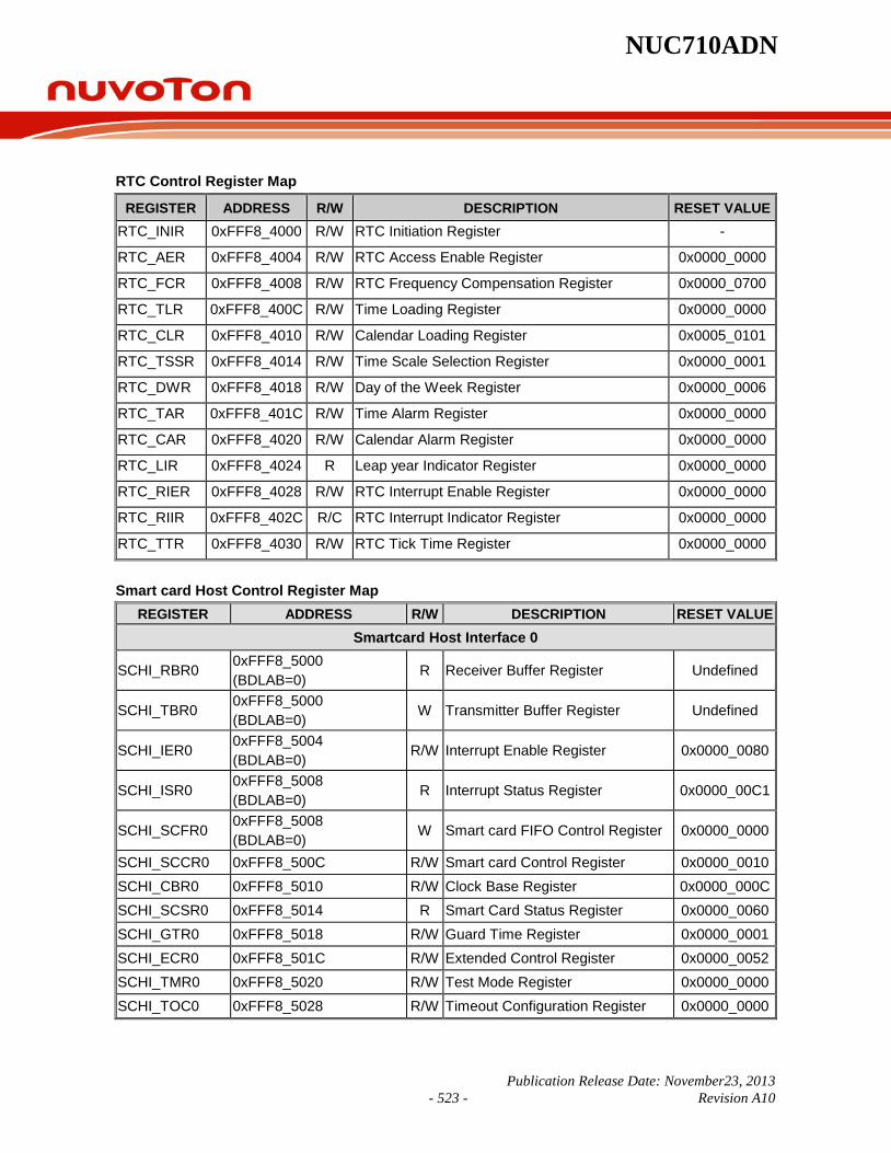
NUC710ADN
Publication Release Date: November23, 2013 - 523 - Revision A10
RTC Control Register Map
REGISTER ADDRESS R/W DESCRIPTION RESET VALUE RTC_INIR 0xFFF8_4000 R/W RTC Initiation Register -
RTC_AER 0xFFF8_4004 R/W RTC Access Enable Register 0x0000_0000
RTC_FCR 0xFFF8_4008 R/W RTC Frequency Compensation Register 0x0000_0700
RTC_TLR 0xFFF8_400C R/W Time Loading Register 0x0000_0000
RTC_CLR 0xFFF8_4010 R/W Calendar Loading Register 0x0005_0101
RTC_TSSR 0xFFF8_4014 R/W Time Scale Selection Register 0x0000_0001
RTC_DWR 0xFFF8_4018 R/W Day of the Week Register 0x0000_0006
RTC_TAR 0xFFF8_401C R/W Time Alarm Register 0x0000_0000
RTC_CAR 0xFFF8_4020 R/W Calendar Alarm Register 0x0000_0000
RTC_LIR 0xFFF8_4024 R Leap year Indicator Register 0x0000_0000
RTC_RIER 0xFFF8_4028 R/W RTC Interrupt Enable Register 0x0000_0000
RTC_RIIR 0xFFF8_402C R/C RTC Interrupt Indicator Register 0x0000_0000
RTC_TTR 0xFFF8_4030 R/W RTC Tick Time Register 0x0000_0000
Smart card Host Control Register Map REGISTER ADDRESS R/W DESCRIPTION RESET VALUE
Smartcard Host Interface 0
SCHI_RBR0 0xFFF8_5000 (BDLAB=0)
R Receiver Buffer Register Undefined
SCHI_TBR0 0xFFF8_5000 (BDLAB=0)
W Transmitter Buffer Register Undefined
SCHI_IER0 0xFFF8_5004 (BDLAB=0)
R/W Interrupt Enable Register 0x0000_0080
SCHI_ISR0 0xFFF8_5008 (BDLAB=0)
R Interrupt Status Register 0x0000_00C1
SCHI_SCFR0 0xFFF8_5008 (BDLAB=0)
W Smart card FIFO Control Register 0x0000_0000
SCHI_SCCR0 0xFFF8_500C R/W Smart card Control Register 0x0000_0010 SCHI_CBR0 0xFFF8_5010 R/W Clock Base Register 0x0000_000C SCHI_SCSR0 0xFFF8_5014 R Smart Card Status Register 0x0000_0060 SCHI_GTR0 0xFFF8_5018 R/W Guard Time Register 0x0000_0001 SCHI_ECR0 0xFFF8_501C R/W Extended Control Register 0x0000_0052 SCHI_TMR0 0xFFF8_5020 R/W Test Mode Register 0x0000_0000 SCHI_TOC0 0xFFF8_5028 R/W Timeout Configuration Register 0x0000_0000

NUC710ADN
Publication Release Date: November235, 2013 - 524 - Revision A10
Smart card Host Control Register Map continued.
REGISTER ADDRESS R/W DESCRIPTION RESET VALUE
Smartcard Host Interface 0 SCHI_TOIR0_0 0xFFF8_502C R/W Timeout Initial Register 0 0x0000_0000 SCHI_TOIR1_0 0xFFF8_5030 R/W Timeout Initial Register 1 0x0000_0000 SCHI_TOIR2_0 0xFFF8_5034 R/W Timeout Initial Register 2 0x0000_0000 SCHI_TOD0_0 0xFFF8_5038 R Timeout Data Register 0 0x0000_00FF SCHI_TOD1_0 0xFFF8_503C R Timeout Data Register 1 0x0000_00FF SCHI_TOD2_0 0xFFF8_5040 R Timeout Data Register 2 0x0000_00FF SCHI_BTOR_0 0xFFF8_5044 R/W Buffer Timeout Data Register 0x0000_0000
SCHI_BLL_0 0xFFF8_5000
(BDLAB=1) R/W Baud Rate Divisor Latch Lower Byte
Register 0x0000_001F
SCHI_BLH_0 0xFFF8_5004
(BDLAB=1) R/W Baud Rate Divisor Latch Higher Byte
Register 0x0000_0000
SCHI_ID_0 0xFFF8_5008
(BDLAB=1) R Smart Card ID Number Register 0x0000_0070
Smartcard Host Interface 1
SCHI_RBR1 0xFFF8_5800
(BDLAB=0) R Receiver Buffer Register Undefined
SCHI_TBR1 0xFFF8_5800
(BDLAB=0) W Transmitter Buffer Register Undefined
SCHI_IER1 0xFFF8_5804
(BDLAB=0) R/W Interrupt Enable Register 0x0000_0080
SCHI_ISR1 0xFFF8_5808
(BDLAB=0) R Interrupt Status Register 0x0000_00C1
SCHI_SCFR1 0xFFF8_5808
(BDLAB=0) W Smart card FIFO Control Register 0x0000_0000
SCHI_SCCR1 0xFFF8_580C R/W Smart card Control Register 0x0000_0010 SCHI_CBR1 0xFFF8_5810 R/W Clock Base Register 0x0000_000C SCHI_SCSR1 0xFFF8_5814 R Smart Card Status Register 0x0000_0060 SCHI_GTR1 0xFFF8_5818 R/W Guard Time Register 0x0000_0001 SCHI_ECR1 0xFFF8_581C R/W Extended Control Register 0x0000_0052 SCHI_TMR1 0xFFF8_5820 R/W Test Mode Register 0x0000_0000 SCHI_TOC1 0xFFF8_5828 R/W Timeout Configuration Register 0x0000_0000 SCHI_TOIR0_1 0xFFF8_582C R/W Timeout Initial Register 0 0x0000_0000 SCHI_TOIR1_1 0xFFF8_5830 R/W Timeout Initial Register 1 0x0000_0000 SCHI_TOIR2_1 0xFFF8_5834 R/W Timeout Initial Register 2 0x0000_0000
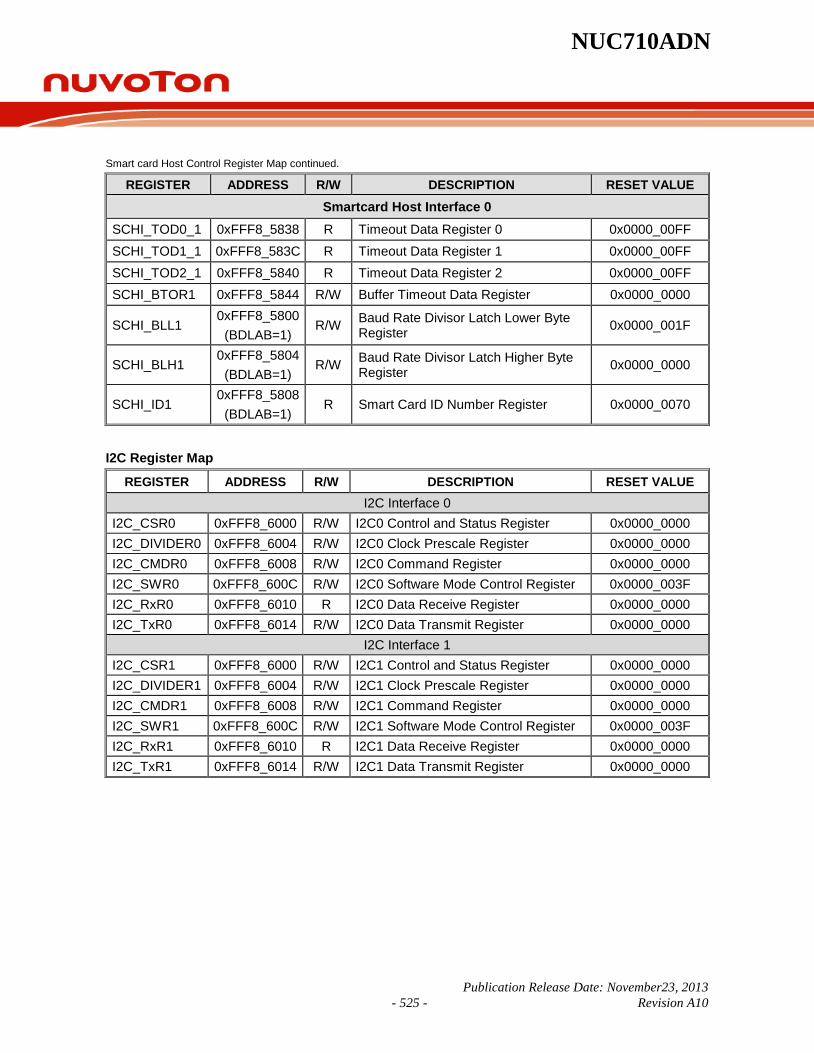
NUC710ADN
Publication Release Date: November23, 2013 - 525 - Revision A10
Smart card Host Control Register Map continued.
REGISTER ADDRESS R/W DESCRIPTION RESET VALUE
Smartcard Host Interface 0 SCHI_TOD0_1 0xFFF8_5838 R Timeout Data Register 0 0x0000_00FF SCHI_TOD1_1 0xFFF8_583C R Timeout Data Register 1 0x0000_00FF SCHI_TOD2_1 0xFFF8_5840 R Timeout Data Register 2 0x0000_00FF SCHI_BTOR1 0xFFF8_5844 R/W Buffer Timeout Data Register 0x0000_0000
SCHI_BLL1 0xFFF8_5800
(BDLAB=1) R/W Baud Rate Divisor Latch Lower Byte
Register 0x0000_001F
SCHI_BLH1 0xFFF8_5804
(BDLAB=1) R/W Baud Rate Divisor Latch Higher Byte
Register 0x0000_0000
SCHI_ID1 0xFFF8_5808
(BDLAB=1) R Smart Card ID Number Register 0x0000_0070
I2C Register Map
REGISTER ADDRESS R/W DESCRIPTION RESET VALUE I2C Interface 0
I2C_CSR0 0xFFF8_6000 R/W I2C0 Control and Status Register 0x0000_0000 I2C_DIVIDER0 0xFFF8_6004 R/W I2C0 Clock Prescale Register 0x0000_0000 I2C_CMDR0 0xFFF8_6008 R/W I2C0 Command Register 0x0000_0000 I2C_SWR0 0xFFF8_600C R/W I2C0 Software Mode Control Register 0x0000_003F I2C_RxR0 0xFFF8_6010 R I2C0 Data Receive Register 0x0000_0000 I2C_TxR0 0xFFF8_6014 R/W I2C0 Data Transmit Register 0x0000_0000
I2C Interface 1 I2C_CSR1 0xFFF8_6000 R/W I2C1 Control and Status Register 0x0000_0000 I2C_DIVIDER1 0xFFF8_6004 R/W I2C1 Clock Prescale Register 0x0000_0000 I2C_CMDR1 0xFFF8_6008 R/W I2C1 Command Register 0x0000_0000 I2C_SWR1 0xFFF8_600C R/W I2C1 Software Mode Control Register 0x0000_003F I2C_RxR1 0xFFF8_6010 R I2C1 Data Receive Register 0x0000_0000 I2C_TxR1 0xFFF8_6014 R/W I2C1 Data Transmit Register 0x0000_0000
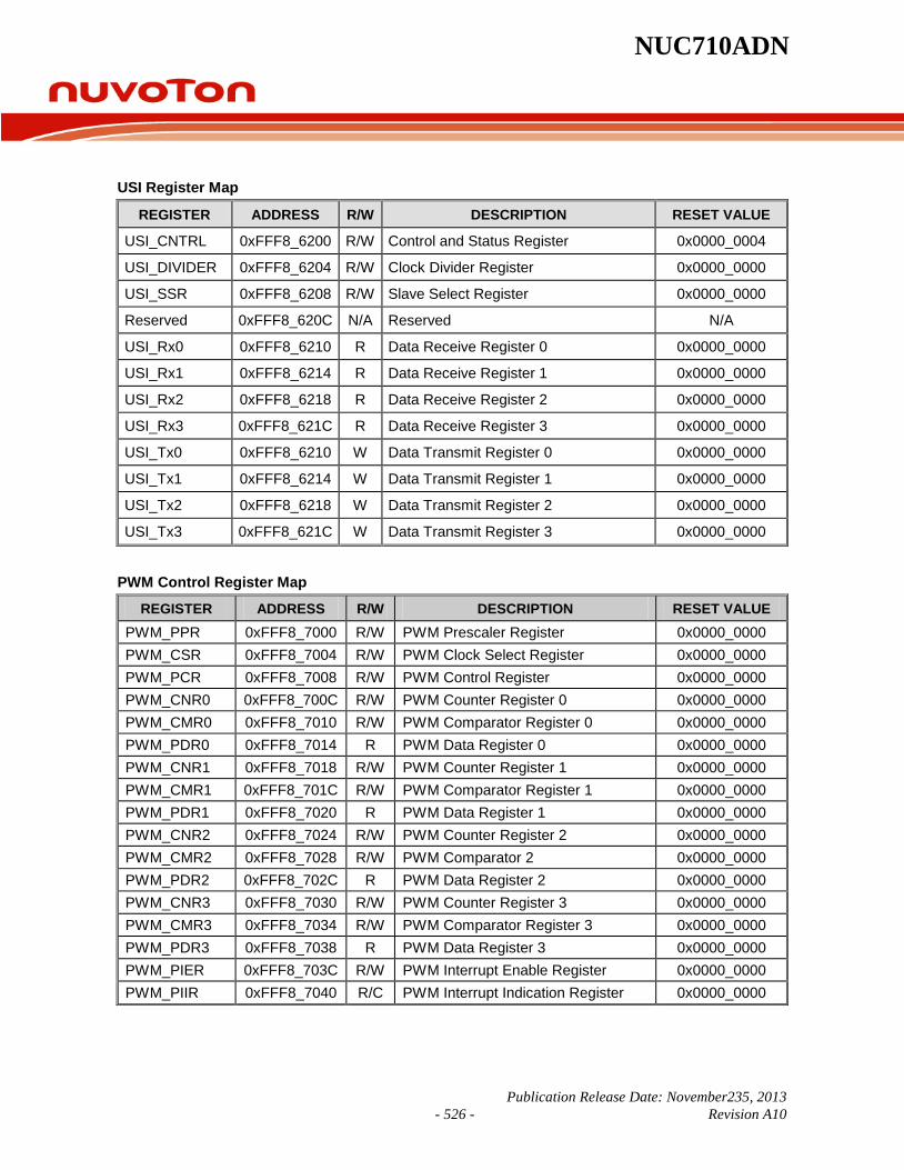
NUC710ADN
Publication Release Date: November235, 2013 - 526 - Revision A10
USI Register Map
REGISTER ADDRESS R/W DESCRIPTION RESET VALUE
USI_CNTRL 0xFFF8_6200 R/W Control and Status Register 0x0000_0004
USI_DIVIDER 0xFFF8_6204 R/W Clock Divider Register 0x0000_0000
USI_SSR 0xFFF8_6208 R/W Slave Select Register 0x0000_0000
Reserved 0xFFF8_620C N/A Reserved N/A
USI_Rx0 0xFFF8_6210 R Data Receive Register 0 0x0000_0000
USI_Rx1 0xFFF8_6214 R Data Receive Register 1 0x0000_0000
USI_Rx2 0xFFF8_6218 R Data Receive Register 2 0x0000_0000
USI_Rx3 0xFFF8_621C R Data Receive Register 3 0x0000_0000
USI_Tx0 0xFFF8_6210 W Data Transmit Register 0 0x0000_0000
USI_Tx1 0xFFF8_6214 W Data Transmit Register 1 0x0000_0000
USI_Tx2 0xFFF8_6218 W Data Transmit Register 2 0x0000_0000
USI_Tx3 0xFFF8_621C W Data Transmit Register 3 0x0000_0000
PWM Control Register Map
REGISTER ADDRESS R/W DESCRIPTION RESET VALUE PWM_PPR 0xFFF8_7000 R/W PWM Prescaler Register 0x0000_0000 PWM_CSR 0xFFF8_7004 R/W PWM Clock Select Register 0x0000_0000 PWM_PCR 0xFFF8_7008 R/W PWM Control Register 0x0000_0000 PWM_CNR0 0xFFF8_700C R/W PWM Counter Register 0 0x0000_0000 PWM_CMR0 0xFFF8_7010 R/W PWM Comparator Register 0 0x0000_0000 PWM_PDR0 0xFFF8_7014 R PWM Data Register 0 0x0000_0000 PWM_CNR1 0xFFF8_7018 R/W PWM Counter Register 1 0x0000_0000 PWM_CMR1 0xFFF8_701C R/W PWM Comparator Register 1 0x0000_0000 PWM_PDR1 0xFFF8_7020 R PWM Data Register 1 0x0000_0000 PWM_CNR2 0xFFF8_7024 R/W PWM Counter Register 2 0x0000_0000 PWM_CMR2 0xFFF8_7028 R/W PWM Comparator 2 0x0000_0000 PWM_PDR2 0xFFF8_702C R PWM Data Register 2 0x0000_0000 PWM_CNR3 0xFFF8_7030 R/W PWM Counter Register 3 0x0000_0000 PWM_CMR3 0xFFF8_7034 R/W PWM Comparator Register 3 0x0000_0000 PWM_PDR3 0xFFF8_7038 R PWM Data Register 3 0x0000_0000 PWM_PIER 0xFFF8_703C R/W PWM Interrupt Enable Register 0x0000_0000 PWM_PIIR 0xFFF8_7040 R/C PWM Interrupt Indication Register 0x0000_0000
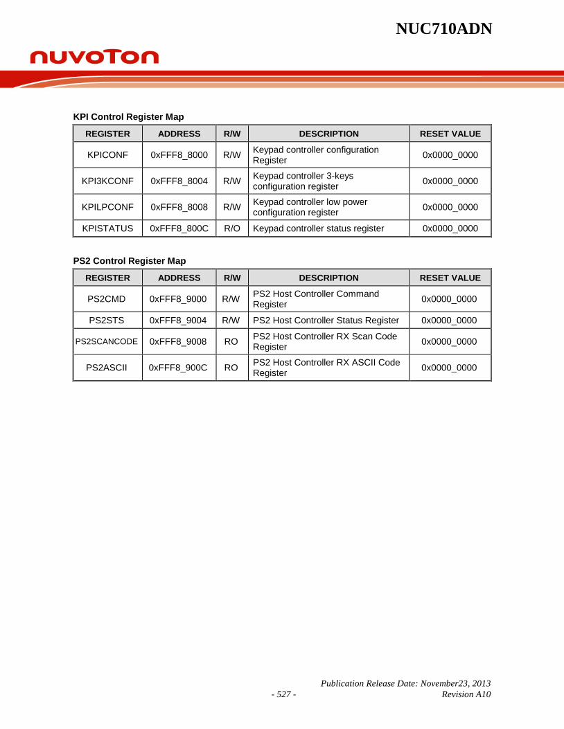
NUC710ADN
Publication Release Date: November23, 2013 - 527 - Revision A10
KPI Control Register Map
REGISTER ADDRESS R/W DESCRIPTION RESET VALUE
KPICONF 0xFFF8_8000 R/W Keypad controller configuration Register 0x0000_0000
KPI3KCONF 0xFFF8_8004 R/W Keypad controller 3-keys configuration register 0x0000_0000
KPILPCONF 0xFFF8_8008 R/W Keypad controller low power configuration register 0x0000_0000
KPISTATUS 0xFFF8_800C R/O Keypad controller status register 0x0000_0000
PS2 Control Register Map
REGISTER ADDRESS R/W DESCRIPTION RESET VALUE
PS2CMD 0xFFF8_9000 R/W PS2 Host Controller Command Register 0x0000_0000
PS2STS 0xFFF8_9004 R/W PS2 Host Controller Status Register 0x0000_0000
PS2SCANCODE 0xFFF8_9008 RO PS2 Host Controller RX Scan Code Register 0x0000_0000
PS2ASCII 0xFFF8_900C RO PS2 Host Controller RX ASCII Code Register 0x0000_0000
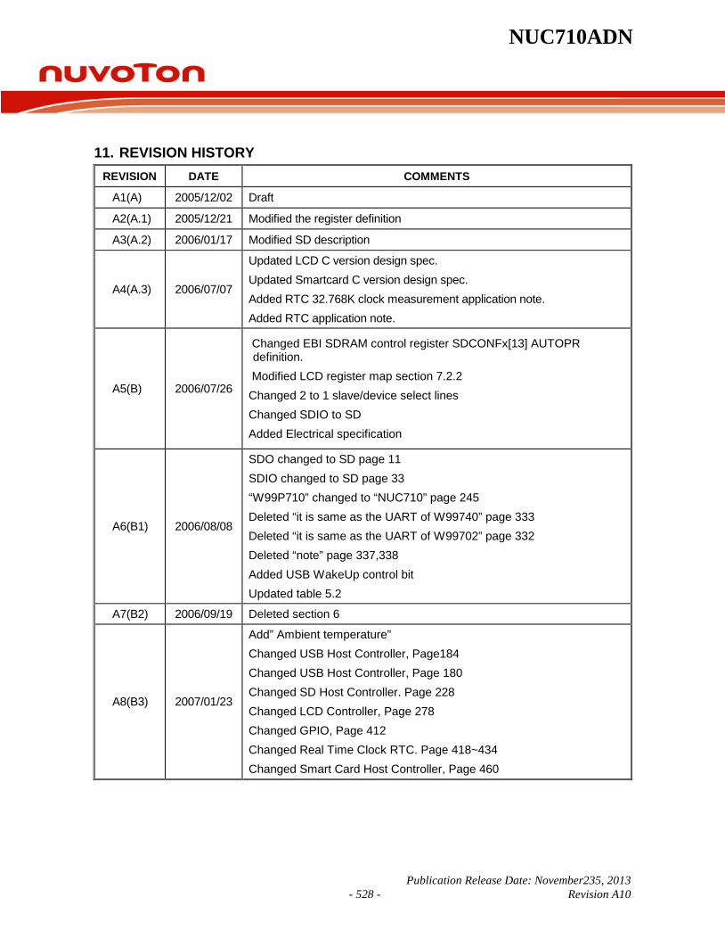
NUC710ADN
Publication Release Date: November235, 2013 - 528 - Revision A10
11. REVISION HISTORY REVISION DATE COMMENTS
A1(A) 2005/12/02 Draft
A2(A.1) 2005/12/21 Modified the register definition
A3(A.2) 2006/01/17 Modified SD description
A4(A.3) 2006/07/07
Updated LCD C version design spec. Updated Smartcard C version design spec. Added RTC 32.768K clock measurement application note. Added RTC application note.
A5(B) 2006/07/26
Changed EBI SDRAM control register SDCONFx[13] AUTOPR definition.
Modified LCD register map section 7.2.2 Changed 2 to 1 slave/device select lines Changed SDIO to SD Added Electrical specification
A6(B1) 2006/08/08
SDO changed to SD page 11 SDIO changed to SD page 33 “W99P710” changed to “NUC710” page 245 Deleted “it is same as the UART of W99740” page 333 Deleted “it is same as the UART of W99702” page 332 Deleted “note” page 337,338 Added USB WakeUp control bit Updated table 5.2
A7(B2) 2006/09/19 Deleted section 6
A8(B3) 2007/01/23
Add” Ambient temperature” Changed USB Host Controller, Page184 Changed USB Host Controller, Page 180 Changed SD Host Controller. Page 228 Changed LCD Controller, Page 278 Changed GPIO, Page 412 Changed Real Time Clock RTC. Page 418~434 Changed Smart Card Host Controller, Page 460

NUC710ADN
Publication Release Date: November23, 2013 - 529 - Revision A10
Revision History, continued
REVISION DATE COMMENTS
A9(B4) 2007/07/20 1. Correct table 5.1 (nWBE2/GPIO 68, nWBE3/GPIO69)
2. Correct Table 6.15.1 (ADD VD[8:17] to PORT 2)
A10 2008/05/05
1. Update ICC1 and ICC2 operation supply current. Page 490
2. Add IPD1 and IPD2 power down mode supply current. Page 491
3. Correct EBI/(ROM/SRAM/External I/O) AC timing TDH and TDSU. Page 494
4. Add new control bit PUP_DIS to disable D15-D0 pin internal pull up resistors in Power Management Control Register (PMCON).
5. Add USB host power down wake up status bits, PDWKS2 and PDWKS2 to Host Controller Root Hub Stats Register (HcRhStstus).
6. Add a new control bit POL to decide SCLK pin polarity when serial clock is stopped in USI Control and Status Register (USI_CNTRL)

NUC710ADN
Publication Release Date: November235, 2013 - 530 - Revision A10
Important Notice Nuvoton Products are neither intended nor warranted for usage in systems or equipment, any malfunction or failure of which may cause loss of human life, bodily injury or severe property damage. Such applications are deemed, “Insecure Usage”.
Insecure usage includes, but is not limited to: equipment for surgical implementation, atomic energy control instruments, airplane or spaceship instruments, the control or operation of dynamic, brake or safety systems designed for vehicular use, traffic signal instruments, all types of safety devices, and other applications intended to support or sustain life.
All Insecure Usage shall be made at customer’s risk, and in the event that third parties lay claims to Nuvoton as a result of customer’s Insecure Usage, customer shall indemnify the damages and liabilities thus incurred by Nuvoton.