nsf csmc summer undergraduate research program:...
TRANSCRIPT

NSF CSMC Summer Undergraduate Research Program: Sustainable MAterials Research Training Camp:
'SMART' Camp University of Oregon
June 18th – June 22nd, 2012
The purpose of SMART camp is to introduce the concepts, specific skills and experimental techniques generally important to solid state chemistry and specific to research undertaken in the Center for Sustainable Materials Chemistry (CSMC), providing hands-on reinforcement of these concepts through lab activities. Over the week you will be acquainted with the theory and experimental practice of topics important to solid state research, including synthesis, crystal chemistry, and solid state properties, and how these are determined and measured using modern experimental techniques and equipment. Mornings will be largely devoted to introducing topics and background important for understanding solid state chemistry and CSMC research, and afternoons are slated for synthesis of a variety of materials and characterization of these materials using equipment in the Center for Advanced Materials Characterization of Oregon (CAMCOR). For example, an introduction to crystal chemistry and x-ray diffraction in the morning will be followed by the opportunity to collect and analyze x-ray diffraction data (for samples synthesized in the first two days) using equipment in CAMCOR. Topics to be discussed and explored include synthetic techniques, structural analysis, compositional analysis, surface analytical techniques, electron microscopy, and optical, magnetic and electrical properties.
You will each receive a copy of the book, Reactions and Characterization of Solids by Sandra E. Dann (Wiley-Interscience, Royal Society of Chemistry, 2002) to take with you. Recommended reading assignments each evening will make the next day’s activities more understandable. Along with this schedule, you also have been sent a packet which includes laboratory procedures for the solid-state synthesis of a high-temperature superconductor and the aqueous synthesis of a ZnO thin film and the optional synthesis activities. We ask that you complete the calculations needed for the superconductor synthesis by Friday, June 15 and email them to Chris Knutson ([email protected]), to ensure that you will be ready to participate when you arrive. We will meet every morning at 9 am in Room 107 Klamath for lectures and a preview of the day’s activities. After a break for lunch on your own, we will reconvene for laboratory activities, ending the day around 5 pm. Sunday June 17: You will be arriving at various times on Sunday June 17. When you get to the dorm (Clark Hall in the Walton Complex) you can check in, unpack and settle in. For our first group activity, we will meet on lawn in front of the dorm at 4 pm for a quick campus tour and pizza dinner on Sunday evening. On our walk across campus we will show you where to meet Monday morning for the start of SMART Camp, and then go to Pegasus Pizza, 790 E 12th for dinner at 5pm.
On the following pages you will find a brief outline of the schedule.

Monday June 18: Synthesis of Solid State Materials
9:00–9:15 Klamath 107
Center for Sustainable Materials Chemistry Overview
9:15–10:45 Klamath 107
Synthesis of Solids and Films (Chris Knutson)
11:00–12:00 Laboratory Safety (Steve Stuckmeyer) 1:15 – 2:30 2:30 – 5:00 Lokey Labs
Lab Activities: Weighing reagents (Klamath 127– Meet in Klamath 107) Synthesis of YBa2Cu3O7 superconductor (Semiconductor Lab), ZnO Film Prep
Tuesday, June 19: Crystal Chemistry and X-‐ray diffraction 9:00 – 10:00 Klamath 107
Basic Crystal Chemistry (Anthony Diaz)
10:00 – 10:45: Lokey Lab
Hands-‐On – Introduction to CrystalMaker Software
10:45 – 11:35 Lokey Lab
X-‐Ray Diffraction (Cathy Page)
11:35 – 12:00 Lokey Lab
Hands-‐On– Introduction to CrystalDiffract Software
1:15 – 4:00 Semiconductor lab
Lab activities: Rotation 1 – Regrind YBa2Cu3O7, press pellets for final firing Rotation 2 – ZnO Device Preparation Rotation 3 – Group Choice* Rotation 4 – Group Choice*
4:00 – 5:00 Overview of Characterization Laboratories and Scheduling
Any free time: (ISCI computers) Hands-‐On: Introduction to CrystalMaker and Crystal Diffract Software
6:00 Dinner at Cathy Page's house: 1631 E 26th Ave. Wednesday, June 20: Electronic and Optical Properties
9:00 – 10:15: Klamath 107
Electrical Properties, Measurements and Devices (Chris Knutson)
10:30 – 11:30 Optical Properties (Anthony Diaz)
11:30 – 12:00 Semiconductor lab
Lab Activities: Finishing up prep work, samples for characterization
1:15 – 5:00 Lokey Labs
Characterization rotations.
Any free time: (ISCI computers) Hands-‐On: Introduction to CrystalMaker and Crystal Diffract Software

Thursday, June 21: Thin Film Characterization, Superconductivity 9:00 – 10:00 Klamath 107
X-‐ray Reflectivity, Ellipsometry (Colby Heideman, Chris Knutson)
10:00 – 11:00 Klamath 107
Other Thin Film Characterization Techniques (Matt Beekman)
11:00 -‐ 12:00 Klamath 107
Superconductivity (Cathy Page)
1:15 – 5:00 Lokey Labs
Characterization rotations.
Down time: (ISCI computers) Hands-‐On: Introduction to CrystalMaker and Crystal Diffract Software
Friday June 22
9 – 10:15 Klamath 107
Friday Presentations: Most Exciting, Memorable or Educational Powerpoints (participants)
10:15 – 11:00 Tying up loose ends! 11:00 – 5:00 Scenic field trip.
Your dorm rooms are available through Saturday morning. Check out time is noon on Saturday, June 23. You will have access to meals through Saturday morning.
* Choice Activities: 1) Preparation of inverse synthetic opals 2) Preparation of silver nanoprisms 3) Nickel nanowires

Recommended Reading Assignments for SMART Camp From Reactions and Characterization of Solids by Sandra E. Dann (Wiley-Interscience, Royal Society of Chemistry, 2002) For Day 1: Chapter 4: Preparation of Materials in the Solid State
4.1 High Temperature Method 4.2 Sealed Tubes 4.3 Controlled Atmospheres 4.4 Hydrothermal Methods 4.5 High Pressure 4.6 Single Crystals 4.7 Nanomaterials 4.8 Amorphous Materials 4.9 Phase Diagrams and Melt Reactions
For Day 2: Chapter 1: Solid State Structure
1.1 Types of Solid 1.2 Properties of Large Crystals 1.3 Crystal Lattices 1.4 Unit Cells and Symmetry Elements 1.5 Structures Formed by Close Packing of Spheres 1.6 Ionic Radius Ratios and Predicting Structure
Chapter 3: Characterization of Solids
3.1 X-ray Diffraction
For Days 3,4,5: Chapter 5: Electronic and Magnetic Behavior of Solids 5.2.1 Band Theory 5.2.2 Superconductivity Chapter 7: Selected Topics 7.1 Superconductivity Chapter 3: Characterization of Solids
3.1 X-ray Diffraction 3.3 Electron Microscopy

SYNTHESIS OF YBa2Cu3O7 A HIGH TEMPERATURE SUPERCONDUCTOR ADAPTED FROM "SYNTHESIS AND TECHNIQUE IN INORGANIC CHEMISTRY, 3rd ED" BY GREGORY S. GIROLAMI, THOMAS B. RAUCHFUSS, AND ROBERT J. ANGELICI Note: Avoid the use of metal spatulas throughout this experiment; metal impurities diminish the superconducting properties of the product. The reactants used in this experiment are mildly toxic, and the dusts should not be inhaled. Avoid eye or skin contact and wash your hands after handling the powders. 1. Synthesis Day 1. Weigh out the calculated quantities of the Y2O3, BaCO3, and CuO powders. In a hood combine the powders in a clean mortar and grind the mixture with a clean pestle until the are thoroughly mixed (about 15 min). The final powder will be of a uniform gray color with no lumps. Transfer the powder to a pre-weighed alumina boat and record the total weight of the starting reagents. Place the boat near the center of the tube in the furnace. Heat the sample to 970 °C overnight. Turn off the power to the furnace (the temperature controller should be left on), and allow the temperature to reach 700 °C before opening the furnace to accelerate the cooling. Once the sample has cooled to 200 °C disassemble the apparatus. When the tube is cooled enough to handle, remove it from the furnace. Day 2. The sample should be black, and the particles should be sintered together. Regrind the sample to a fine powder; the particles should be black and lustrous. Reserve a small portion of this powder in a vial for X-ray diffraction analysis later. Using a pellet press, make a 2.5 cm pellet from the remaining powder. Place on an alumina tray for firing. On the tube furnace, fit the ends of the tube with gas adapters connecting one adapter to an oxygen cylinder and the other end to an oil bubbler so that the gas flow can be monitored. Before turning on the furnace, adjust the oxygen flow to 1-2 bubbles per second. Heat to 970°C for ~ 2 hrs, cool to ~550°C for several hours. Ramp the temperature slowly to ~400°C, turn the furnace off and allow to cool. Remove the pellet from the furnace. Taking care not to crack the pellet, scrape a small amount of powder off its surface into a vial for X-ray diffraction analysis. 2. Analysis Meissner Effect. Place some liquid N2 in a petri dish or styrofoam container. Immerse the sintered pellet in the liquid N2. Using a pair of plastic tweezers place a small magnet on the pellet. If the sample is sufficiently cool the magnet should levitate over the pellet. X-ray Diffraction. Perform X-ray Diffraction on the powder samples collected during the analysis. (Further instructions on this during the week.) Compare this to the predicted pattern from the CrystalMaker software. Consider the causes of any discrepancies between the two. Are there extra peaks or peaks missing? How intense are the observed reflections? What is the level of the background signal in the spectrum? Based on what you know of X-ray diffraction and the crystal structure of the material, can you create a hypothesis to explain any discrepancies?

Aqueous Inorganic Inks for Low-Temperature Fabrication ofZnO TFTs
Stephen T. Meyers,† Jeremy T. Anderson,† Celia M. Hung,‡ John Thompson,§
John F. Wager,‡ and Douglas A. Keszler*,†
Department of Chemistry, Oregon State UniVersity, 153 Gilbert Hall, CorVallis,Oregon 97331-4003, School of Electrical Engineering and Computer Science, Oregon StateUniVersity, CorVallis, Oregon 97331-5501, and Hewlett-Packard Company, 1000 NE Circle
BouleVard, CorVallis, Oregon 97330
Received October 20, 2008; E-mail: [email protected]
Abstract: A simple, low-cost, and nontoxic aqueous ink chemistry is described for digital printing of ZnOfilms. Selective design through controlled precipitation, purification, and dissolution affords an aqueousZn(OH)x(NH3)y
(2-x)+ solution that is stable in storage, yet promptly decomposes at temperatures below 150°C to form wurtzite ZnO. Dense, high-quality, polycrystalline ZnO films are deposited by ink-jet printingand spin-coating, and film structure is elucidated via X-ray diffraction and electron microscopy. Semiconduc-tor film functionality and quality are examined through integration in bottom-gate thin-film transistors.Enhancement-mode TFTs with ink-jet printed ZnO channels annealed at 300 °C are found to exhibit strongfield effect and excellent current saturation in tandem with incremental mobilities from 4-6 cm2 V-1 s-1.Spin-coated ZnO semiconductors processed at 150 °C are integrated with solution-deposited aluminumoxide phosphate dielectrics in functional transistors, demonstrating both high performance, i.e., mobilitiesup to 1.8 cm2 V-1 s-1, and the potential for low-temperature solution processing of all-oxide electronics.
Introduction
A convergence of electronic and chemical properties in ZnOmake it one of the more widely used metal oxides withapplications ranging from catalysis to cosmetics, fungicides tophosphors, and pigments to polymer additives. In recent years,the material has garnered additional attention as a channelmaterial for high-performance transparent thin-film transistors(TFTs). Part of a large class of semiconducting oxides,1,2 thefacile thin-film processing of ZnO has enabled physical vapordeposition (PVD) fabrication of ZnO TFTs with a wide varietyof gate dielectrics, even extending to flexible substrates.3-5 Sincethe beginning of this ZnO TFT renaissance (the first ZnO TFTwas proposed in 1968),6 a coincident effort has been made todevelop solution-based methods for large-area, low-cost, andlow-temperature printing of ZnO films for macroelectronicapplications. These efforts, however, have been hampered by alack of solution precursors appropriate for a high-speed, low-temperature printing process. The defect and solution chemistriesof ZnO, vital to electrical performance and film quality, havebeen too often ignored in favor of the ready application of
conventional metal-organic preparative routes common toceramic synthesis. In the present contribution, we demonstratea simple aqueous precursor specifically designed to takeadvantage of the unique solution chemistry of Zn. This nontoxic,aqueous chemistry generates high-quality ZnO films at lowtemperatures, allowing ink-jet printing of high-performanceZnO-channel TFTs at 150 °C.
Such chemistries have not previously been demonstrated,despite the voluminous literature concerning solution-processedZnO thin films. Instead, the condensation and crystallization ofZnO from aqueous solutions has been utilized in more circuitousroutes to nanocrystalline films. Reports of chemical bathdeposition (CBD) are prevalent, though this process is incom-patible with high-speed printing. Moreover, although carefulattention to CBD thermodynamics permits the deposition of ZnOfilms at temperatures below 100 °C,7 TFTs fabricated by thismethod have until recently8 performed very poorly in theabsence of high-temperature annealing.9,10 The deposition andsintering of nanoparticle suspensions following a procedure ofdecoupled growth and deposition is also quite common.11 Low-temperature sintering, however, typically results in porousnanoparticle agglomerates with a preponderance of interface† Department of Chemistry, Oregon State University.
‡ School of Electrical Engineering and Computer Science, Oregon StateUniversity.
§ Hewlett-Packard Company.(1) Hosono, H. J. Non-Cryst. Solids 2006, 352, 851.(2) Chiang, H. Q.; Wager, J. F.; Hoffman, R. L.; Jeong, J.; Keszler, D. A.
Appl. Phys. Lett. 2005, 86, 013503.(3) Hoffman, R. L.; Norris, B. J.; Wager, J. F. Appl. Phys. Lett. 2003, 82,
733.(4) Carcia, P. F.; McLean, R. S.; Reilly, M. H. Appl. Phys. Lett. 2006,
88, 123509.(5) Carcia, P. F.; McLean, R. S.; Reilly, M. H. J. SID. 2005, 13, 547.(6) Boesoen, G. F.; Jacobs, J. E. Proc. IEEE 1968, 56, 2094.
(7) Govender, K.; Boyle, D. S.; Kenway, P. B.; O’Brien, P. J. Mater.Chem. 2004, 14, 2575.
(8) Li, C.; Li, Y.; Wu, Y.; Ong, B. S.; Loutfy, R. O. J. Appl. Phys. 2007,102, 076101.
(9) Cheng, H.; Chen, C.; Lee, C. Thin Solid Films. 2006, 498, 142.(10) Redinger, D.; Subramanian, V. IEEE Trans. Electron DeVices 2007,
54, 1301.(11) Volkman, S. K.; Mattis, B. A.; Molesa, S. E.; Lee, J. B.; de la Fuente
Vombeck, A.; Bakhishev, T.; Subramanian, V. IEEE Int. ElectronDeVice Meeting Tech. Dig. 2004, 769.
Published on Web 12/03/2008
10.1021/ja808243k CCC: $40.75 2008 American Chemical Society J. AM. CHEM. SOC. 2008, 130, 17603–17609 9 17603

states that not only limit carrier mobility, but also adverselyaffect TFT subthreshold slope, off current, and switchingvoltage. Hybrid approaches using combinations of alignednanoparticles, sol-gel,12 and CBD13,14 have overcome someof these density issues at the expense of process flexibility; ZnOTFTs processed at 270 °C, for example, have exhibitedsaturation mobilities up to 1.3 cm2 V-1 s-1.15 Yet, to date, allpurely chemical precursors compatible with high-speed directprinting require high-temperature (g500 °C) processing,16-19
reflective of the high activation and diffusion energies attendantto metal-organic sol-gel20 and oxidative/hydrolytic21,22 de-composition reactions.
In contrast to these kinetically limited, complex, and energy-intensive processes, we have advanced simple cation hydrationchemistries in designing environmentally benign and highlyreactive aqueous precursors for deposition of very high-qualityoxide films.23,24 Here, purified ammine-hydroxo zinc solutionstap the rapid, low-energy kinetics of metal-ammine dissociationand hydroxide condensation/dehydration reactions to affordcrystallization of ZnO near room temperature. This minimalistapproach to precursor synthesis provides superior film quality,while at the same time enabling high-throughput digital printingvia ink-jet deposition. Building on our previous solutiondeposition of oxide dielectrics, we further demonstrate thepotential for all-oxide printed electronics through fabricationof the first high-performance TFTs containing both solution-processed oxide dielectric and semiconductor layers. A ZnOsemiconductor layer annealed at 150 °C is combined with asolution-processed aluminum oxide phosphate (AlPO) dielectricto yield a device exhibiting a field-effect mobility near 2 cm2
V-1 s-1.
Experimental Methods
Precursor Synthesis and Analysis. Zn solutions were preparedby dissolving Zn(NO3)2 ·6H2O (Alfa Aesar, 99.998%) in distilledH2O to a total concentration of 0.5 M Zn. Ten milliliters of 2.5 MNaOH (Mallinckrodt, ACS) was added dropwise to 15 mL of thissolution over the course of 5 min while stirring vigorously. Theresulting hydroxide slurry was centrifuged and the supernatantremoved. The hydrated precipitate was then suspended in 20 mLof H2O and agitated for 2 min, followed by centrifugation andsupernatant removal. Rinse and separation steps were repeated fouradditional times to minimize Na+ and NO3
- concentrations.
Following final centrifugation, the supernatant was decanted a finaltime and the hydrated precipitate dissolved in 50 mL of 6.6 MNH3(aq) (Alfa Aesar, 99.99%) to form a stock precursor. The finalZn concentration in the stock precursor solution was 0.14 M.Millipore H2O with a minimum resistivity of 18 MΩ was used forall dilutions and rinses. Na and impurity concentration data weregenerated with a Perkin-Elmer 3000DV inductively coupled plasmaoptical emission spectrometer (ICP-OES). Reported data representthe mean of three consecutive replicate measurements using aminimum of two check standards to bracket measured concentra-tions. Bulk ZnO powders were produced for X-ray diffraction(XRD) measurements by placing a known volume of the precursorsolution in a glass vial, evaporating the solvent, and dehydratingthe resulting powder in a drying oven in air for 24 h at 50 °C.Powder XRD data were collected by using a Siemens D5000diffractometer with Cu KR radiation.
Film Preparation and Analysis. Thin films were deposited byspin-coating the stock precursor solution filtered through a 0.45-µm PTFE syringe filter. Substrate rotation speed and time were3000 rpm and 30 s. The film was then immediately cured on apreheated hot plate at selected temperatures between 150 and 500°C for 5-10 min. Inks for thermal ink-jet (TIJ) printing wereprepared by dilution of the stock solution with isopropanol (Aldrich,99.5% ACS), aqueous ammonia, and H2O to a final concentrationof 5.3 M NH3(aq), 0.056 M Zn, and 40% (vol) isopropanol.Isopropanol is used solely to decrease solution surface tension toallow reliable jetting. Films were printed by promptly fillingcommercial Hewlett-Packard (HP-80) printer cartridges and printing1 × 15 mm2 lines directly onto precleaned substrates at roomtemperature. Printing was followed by immediate hot-plate curingin air for 5-10 min at selected temperatures between 150 and 500°C. Coating and curing steps were repeated as necessary to obtainthe desired thickness. A final anneal at the same temperature wasdone either in air or in a tube furnace under 150 sccm flowingN2(g) or Ar(g). Thin films for XRD and scanning electron micro-scopy (SEM) were deposited on substrates of 200-nm thickthermally grown SiO2 on Si. All substrates were cleaned bysonication in a 5% solution of Contrad 70 for 45 min at 45 °Cfollowed by thorough rinsing with 18-MΩ H2O. Thin-film XRDdata were collected by using a Rigaku RAPID diffractometer withCu KR radiation.
Device Fabrication and Characterization. Bottom-gate TFTtest structures were fabricated by TIJ printing or spin coating ZnOsemiconductor films of 15-40 nm thickness onto a 100-nm SiO2
gate dielectric thermally grown on p-type Si substrates with 30 nmof Ta and 300 nm of Au on the back side to allow gate probingthrough the substrate. Aluminum oxide phosphate (AlPO) precursorsolutions were prepared as previously reported.24 Sixty-nanometerAlPO gate dielectric films were spin-coated on bare, p+2 Sisubstrates and subjected to a postdeposition anneal at 500 °C for1 h prior to ZnO deposition. One-hundred or 200-nm thick Al sourceand drain contacts were then thermally evaporated via shadow maskonto ZnO films to complete device stacks. All TFTs werecharacterized in the dark under atmospheric conditions by usingHewlett-Packard 4156C and 4155A semiconductor parameteranalyzers; device mobility and operational parameters were evalu-ated following the methods of Hoffman.25
Results and Discussion
Precursor Chemistry and Analysis. The fundamental chemi-cal requirement for any solution printing process is the completeconversion of the precursor ink into a target oxide of the correctphase. All solvents and ligands must be eliminated under thedesired processing conditions and within the thermal budget.Circuitous metal-organic routes typically sacrifice simplicityand reactivity for the sake of perceived improvements in
(12) Cheng, H.-C.; Chen, C.-F.; Tsay, C.-Y. Appl. Phys. Lett. 2007, 90,012113.
(13) Sun, B.; Sirringhaus, H. Nano Lett. 2005, 5, 2408.(14) Sun, B.; Sirringhaus, H. J. Am. Chem. Soc. 2006, 128, 16231.(15) Sun, B.; Peterson, R. L.; Sirringhaus, H.; Mori, K. J. Phys. Chem. C.
2007, 111, 18831.(16) Norris, B. J.; Anderson, J. T.; Wager, J. F.; Keszler, D. A. J. Phys.
D: Appl. Phys. 2003, 36, L105.(17) Lee, J. H.; Lin, P.; Ho, J. C.; Lee, C. C. Electrochem. Solid-State
Lett. 2006, 9, G117.(18) Lee, J. H.; Lin, P.; Ho, J. C.; Lee, C. C.; Wang, Y. W. Jpn. J. Appl.
Phys. 2005, 44, 2005.(19) Ong, B. S.; Li, C.; Li, Y.; Wu, Y.; Loutfy, R. J. Am. Chem. Soc.
2007, 129, 2750.(20) Bhuiyan, M. S.; Paranthaman, M.; Salama, K. Supercond. Sci. Technol.
2006, 19, R1.(21) Chang, Y.-J.; Lee, D.-H.; Herman, G. S.; Chang, C.-H. Electrochem.
Solid-State Lett. 2007, 10, H135.(22) Lee, D.-H.; Chang, Y.-J.; Herman, G. S.; Chang, C.-H. AdV. Mater.
2007, 19, 843.(23) Anderson, J., T.; Keszler, D. A.; Meyers, S. T.; Chiang, H. Q.; Hong,
D.; Presley, R. E.; Wager, J. F. Mater. Res. Soc. Symp. Proc. 2007,988E, 0988.
(24) Meyers, S. T.; Anderson, J., T.; Hong, D.; Hung, C. M.; Wager, J. F.;Keszler, D. A. Chem. Mater. 2007, 19, 4023. (25) Hoffman, R. L. J. Appl. Phys. 2004, 95, 5813.
17604 J. AM. CHEM. SOC. 9 VOL. 130, NO. 51, 2008
A R T I C L E S Meyers et al.
rheological properties.20 The primary result is that otherwiserapid and highly favorable reactions, i.e., the hydrolysis andsubsequent hydroxo-condensation of the metal species, insteadrequire extreme activation and diffusion energies to complete.In contrast, the simplicity and reactivity inherent to aqueousZn chemistry render an all-inorganic hydroxo-condensationapproach extremely attractive. ZnO is amphoteric in nature andthe weak acidity of the Zn2+ ion affords a wide solubility range.The low activation energy required for Zn(OH)2 dehydrationand oxide crystallization is complementary to low-temperaturedeposition, as opposed to the much higher energies requiredfor complete dehydration of hydroxides such as In(OH)3 andSn(OH)4.
26,27 Furthermore, Zn, in common with many borderlineLewis acids, readily forms coordination complexes with am-monia in an aqueous environment. Ammonia is distinguishedfrom other nitrogen-based ligands by its extreme volatility andlabile bonding which afford low-temperature, rapid, and (equallyimportant) low volume-loss decomposition processes. Althoughthe solubility of Zn in aqueous ammonia is relatively high, thekinetic obstacles to oxide dissolution are such that directlydissolving large-grain ZnO powders is difficult. Nevertheless,to fully exploit the excellent low temperature thermodynamicsand rapid kinetics of ammine-hydroxo zinc decomposition,nonbasic counterions must be excluded, prohibiting simpledissolution of Zn salts in aqueous ammonia. To circumvent thisbarrier, fresh Zn(OH)2 precipitates may be purified and directlydissolved in NH3(aq) solutions. Such processes have been usedfor more than 80 years as part of bulk ZnO purification andsynthesis procedures.28 The predominant form of the aqueousammine-hydroxo zinc complex that results depends on theammonia concentration,29 but it may be described by the generalformula Zn(OH)x(NH3)y
(2-x)+. Properly purified, these solutionsare largely free of nonbasic counterion contaminants, andprecipitate a pure phase hydroxide upon ammonia loss, followedby dehydration and oxide crystallization at temperatures below100 °C.
Synthetic conditions in the present study were intended toprovide both a minimal impurity concentration and a low-temperature, nonhydrolytic decomposition mechanism for theinevitable residual ions. Selection of the initial soluble Zn(NO3)2
salt is important in pursuit of the second goal, as polarizationof the NO3
- charge cloud by acidic cations is known to resultin reasonably low decomposition temperatures for nitrate saltsof acidic metal cations.30 A study of zinc ammine hydroxidenitrates by Benard and co-workers31 provides evidence thatZn5(OH)8(NO3)2 ·2NH3 and related compounds offer very lowdecomposition and ZnO crystallization temperatures, generally<150 °C, with NH3 loss occurring well below 100 °C. Theseresults contrast starkly with thermal-analysis studies of zincchloride hydroxide compounds including Zn5(OH)8Cl2 ·H2O and-ZnOHCl by Srivastava and Secco,32 which confirm theexpectation that basic halides not only dehydrate at much highertemperatures than the pure hydroxides, but that hydrolytic oroxidative removal of the residual metal chloride may require
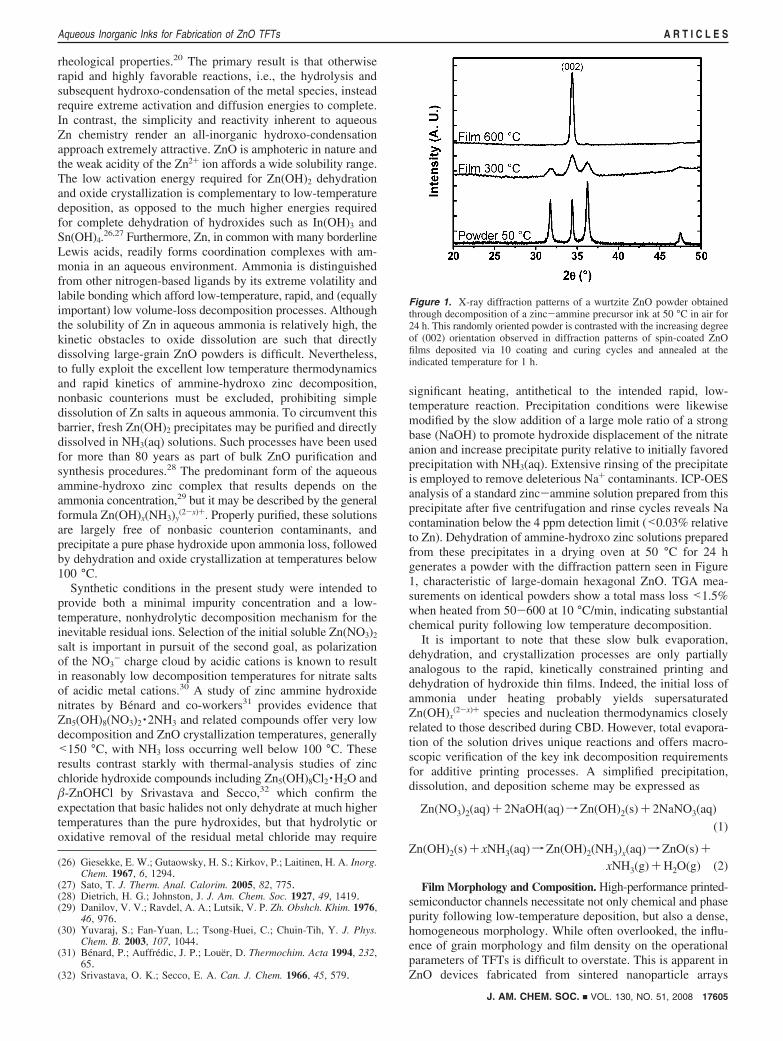
significant heating, antithetical to the intended rapid, low-temperature reaction. Precipitation conditions were likewisemodified by the slow addition of a large mole ratio of a strongbase (NaOH) to promote hydroxide displacement of the nitrateanion and increase precipitate purity relative to initially favoredprecipitation with NH3(aq). Extensive rinsing of the precipitateis employed to remove deleterious Na+ contaminants. ICP-OESanalysis of a standard zinc-ammine solution prepared from thisprecipitate after five centrifugation and rinse cycles reveals Nacontamination below the 4 ppm detection limit (<0.03% relativeto Zn). Dehydration of ammine-hydroxo zinc solutions preparedfrom these precipitates in a drying oven at 50 °C for 24 hgenerates a powder with the diffraction pattern seen in Figure1, characteristic of large-domain hexagonal ZnO. TGA mea-surements on identical powders show a total mass loss <1.5%when heated from 50-600 at 10 °C/min, indicating substantialchemical purity following low temperature decomposition.
It is important to note that these slow bulk evaporation,dehydration, and crystallization processes are only partiallyanalogous to the rapid, kinetically constrained printing anddehydration of hydroxide thin films. Indeed, the initial loss ofammonia under heating probably yields supersaturatedZn(OH)x
(2-x)+ species and nucleation thermodynamics closelyrelated to those described during CBD. However, total evapora-tion of the solution drives unique reactions and offers macro-scopic verification of the key ink decomposition requirementsfor additive printing processes. A simplified precipitation,dissolution, and deposition scheme may be expressed as
Zn(NO3)2(aq)+ 2NaOH(aq)fZn(OH)2(s)+ 2NaNO3(aq)
(1)
Zn(OH)2(s)+ xNH3(aq)fZn(OH)2(NH3)x(aq)fZnO(s)+xNH3(g)+H2O(g) (2)
Film Morphology and Composition. High-performance printed-semiconductor channels necessitate not only chemical and phasepurity following low-temperature deposition, but also a dense,homogeneous morphology. While often overlooked, the influ-ence of grain morphology and film density on the operationalparameters of TFTs is difficult to overstate. This is apparent inZnO devices fabricated from sintered nanoparticle arrays
(26) Giesekke, E. W.; Gutaowsky, H. S.; Kirkov, P.; Laitinen, H. A. Inorg.Chem. 1967, 6, 1294.
(27) Sato, T. J. Therm. Anal. Calorim. 2005, 82, 775.(28) Dietrich, H. G.; Johnston, J. J. Am. Chem. Soc. 1927, 49, 1419.(29) Danilov, V. V.; Ravdel, A. A.; Lutsik, V. P. Zh. Obshch. Khim. 1976,
46, 976.(30) Yuvaraj, S.; Fan-Yuan, L.; Tsong-Huei, C.; Chuin-Tih, Y. J. Phys.
Chem. B. 2003, 107, 1044.(31) Benard, P.; Auffredic, J. P.; Louer, D. Thermochim. Acta 1994, 232,
65.(32) Srivastava, O. K.; Secco, E. A. Can. J. Chem. 1966, 45, 579.
Figure 1. X-ray diffraction patterns of a wurtzite ZnO powder obtainedthrough decomposition of a zinc-ammine precursor ink at 50 °C in air for24 h. This randomly oriented powder is contrasted with the increasing degreeof (002) orientation observed in diffraction patterns of spin-coated ZnOfilms deposited via 10 coating and curing cycles and annealed at theindicated temperature for 1 h.
J. AM. CHEM. SOC. 9 VOL. 130, NO. 51, 2008 17605
Aqueous Inorganic Inks for Fabrication of ZnO TFTs A R T I C L E S
wherein individual nanocrystals may have high mobilities,33,34
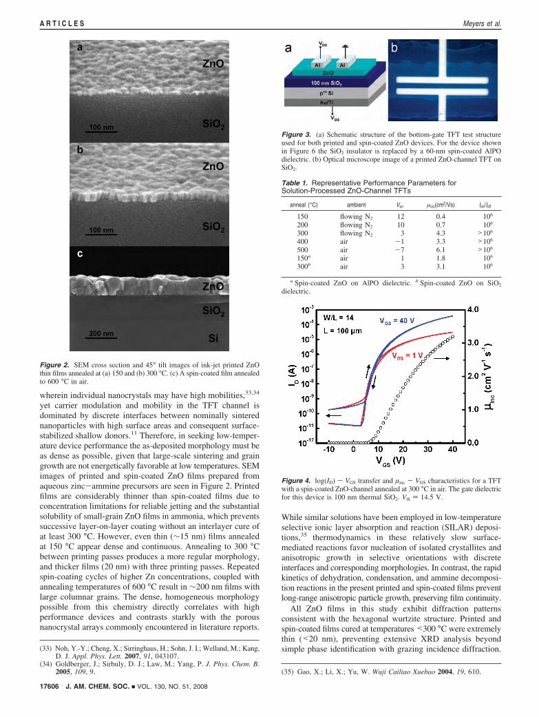
yet carrier modulation and mobility in the TFT channel isdominated by discrete interfaces between nominally sinterednanoparticles with high surface areas and consequent surface-stabilized shallow donors.11 Therefore, in seeking low-temper-ature device performance the as-deposited morphology must beas dense as possible, given that large-scale sintering and graingrowth are not energetically favorable at low temperatures. SEMimages of printed and spin-coated ZnO films prepared fromaqueous zinc-ammine precursors are seen in Figure 2. Printedfilms are considerably thinner than spin-coated films due toconcentration limitations for reliable jetting and the substantialsolubility of small-grain ZnO films in ammonia, which preventssuccessive layer-on-layer coating without an interlayer cure ofat least 300 °C. However, even thin (∼15 nm) films annealedat 150 °C appear dense and continuous. Annealing to 300 °Cbetween printing passes produces a more regular morphology,and thicker films (20 nm) with three printing passes. Repeatedspin-coating cycles of higher Zn concentrations, coupled withannealing temperatures of 600 °C result in ∼200 nm films withlarge columnar grains. The dense, homogeneous morphologypossible from this chemistry directly correlates with highperformance devices and contrasts starkly with the porousnanocrystal arrays commonly encountered in literature reports.
While similar solutions have been employed in low-temperatureselective ionic layer absorption and reaction (SILAR) deposi-tions,35 thermodynamics in these relatively slow surface-mediated reactions favor nucleation of isolated crystallites andanisotropic growth in selective orientations with discreteinterfaces and corresponding morphologies. In contrast, the rapidkinetics of dehydration, condensation, and ammine decomposi-tion reactions in the present printed and spin-coated films preventlong-range anisotropic particle growth, preserving film continuity.
All ZnO films in this study exhibit diffraction patternsconsistent with the hexagonal wurtzite structure. Printed andspin-coated films cured at temperatures <300 °C were extremelythin (<20 nm), preventing extensive XRD analysis beyondsimple phase identification with grazing incidence diffraction.(33) Noh, Y.-Y.; Cheng, X.; Sirringhaus, H.; Sohn, J. I.; Welland, M.; Kang,
D. J. Appl. Phys. Lett. 2007, 91, 043107.(34) Goldberger, J.; Sirbuly, D. J.; Law, M.; Yang, P. J. Phys. Chem. B.
2005, 109, 9. (35) Gao, X.; Li, X.; Yu, W. Wuji Cailiao Xuebao 2004, 19, 610.
Figure 2. SEM cross section and 45° tilt images of ink-jet printed ZnOthin films annealed at (a) 150 and (b) 300 °C. (c) A spin-coated film annealedto 600 °C in air.
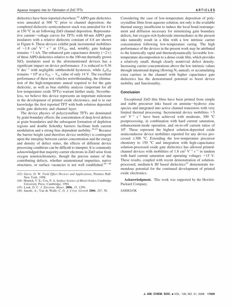
Figure 3. (a) Schematic structure of the bottom-gate TFT test structureused for both printed and spin-coated ZnO devices. For the device shownin Figure 6 the SiO2 insulator is replaced by a 60-nm spin-coated AlPOdielectric. (b) Optical microscope image of a printed ZnO-channel TFT onSiO2.
Table 1. Representative Performance Parameters forSolution-Processed ZnO-Channel TFTs
anneal (°C) ambient Von µinc(cm2/Vs) Ion/Ioff
150 flowing N2 12 0.4 106
200 flowing N2 10 0.7 106
300 flowing N2 3 4.3 >106
400 air -1 3.3 >106
500 air -7 6.1 >106
150a air 1 1.8 106
300b air 3 3.1 106
a Spin-coated ZnO on AlPO dielectric. b Spin-coated ZnO on SiO2
dielectric.
Figure 4. log(ID) - VGS transfer and µinc - VGS characteristics for a TFTwith a spin-coated ZnO-channel annealed at 300 °C in air. The gate dielectricfor this device is 100 nm thermal SiO2. Vth ) 14.5 V.
17606 J. AM. CHEM. SOC. 9 VOL. 130, NO. 51, 2008
A R T I C L E S Meyers et al.

Interlayer curing g300 °C allowed sequential coatings andthicker films. X-ray diffraction patterns obtained from sequen-tially spin-coated ZnO films annealed at 300 and 600 °C aredocumented in Figure 1. As manifest in the prominent (002)reflection observed at 34.4°, these films demonstrate a varyingdegree of c-axis orientation, increasing significantly withadditional deposition cycles and elevated interlayer curingtemperature. Substantial c-axis orientation is frequently reportedfollowing high-temperature deposition of ZnO films from bothsolution and vapor techniques, as grain growth tends to favorthe low energy (002) surface.36 Although not examined in thepresent study, the effect of this texturing on electron mobilityhas been reported to be significant.19
Electrical Characterization. Electrical analyses of ZnO filmswere performed by using the bottom-gate TFT structure depictedin Figure 3a. Device performance is assessed through an analysisof the turn-on voltage (Von), drain current on-to-off ratio(Ion/Ioff), and incremental channel mobility (µinc). Hoffman25 andHong et al.37 have defined Von as the gate voltage at which ID
begins to increase when plotted versus VGS on a logarithmicscale. It is here employed in place of the threshold voltage (Vth)due to its greater precision in the context of TFT characteriza-tion. Poor turn-on (extremely negative or positive Von) charac-teristics are unsuitable for most circuit applications. A lowIon/Ioff ratio prevents the device from operating as a high dynamicrange switch, the primary application for which TFTs are
typically employed. Channel mobility directly relates to TFTcurrent drive and maximum switching frequency, and representsa useful figure of merit provided the former parameters areacceptable. The incremental, or field-effect mobility quoted hereis extracted in linear-regime operation at VDS ) 1 V. A finalparameter, the subthreshold swing (S)sdefined as the gatevoltage required to change the drain current by 1 order ofmagnitude in the subthreshold region of the transfer curvesprovides a measure of how effective applied gate voltage is inturning the channel on and off.38 It is imperative that all ofthese parameters are optimized for a truly useful device; atabulation of solution-deposited ZnO-channel TFT performanceparameters representative of more than 250 devices may befound in Table 1.
TFTs fabricated with spin-coated ZnO channels annealed at300 °C in air on thermally grown SiO2 dielectrics displaypromising operation, as evident from the transfer curves plottedin Figure 4. Strong current switching is observed for all suchdevices, with Von values in the range -2 to 4 V, and consistentfield-effect mobilities >3 cm2 V-1 s-1 (at 40VGS). Ion/Ioff ratiosare ∼106, minimal hysteresis is observed, and for the deviceparameters summarized in Figure 4, S ) 1.3 V dec-1.
Spin-coating is a valuable tool for large-area film deposition,but does not offer digital patterning and additive processingcapabilities essential for high-speed printing applications. Ink-jet printing was therefore used to deposit ZnO channels forintegration into TFTs on thermally grown SiO2. Because of the
(36) Kajikawa, Y. J. Cryst. Growth 2006, 289, 387.(37) Hong, D.; Yerubandi, G.; Chiang, H. Q.; Spiegelberg, M. C.; Wager,
J. F. Crit. ReV. Solid-State Mater. 2008, 33, 101.(38) Schroder, D. K., Semiconductor Material and DeVice Characterization,
2nd ed.; John Wiley and Sons: New York, 1998.
Figure 5. log(ID) - VGS transfer and µinc - VGS characteristics and ID-VDS output curves for ink-jet printed ZnO-channel TFTs on 100-nm thermal SiO2
gate dielectrics.; channel annealed in flowing N2(g) at (a) and (b) 300 °C and (c) and (d) 150 °C. Vth ) 15 and 20 V, respectively.
J. AM. CHEM. SOC. 9 VOL. 130, NO. 51, 2008 17607
Aqueous Inorganic Inks for Fabrication of ZnO TFTs A R T I C L E S

physical constraints of the available commercial cartridges,isopropanol was added to stock zinc-ammine precursors todecrease solution surface tension and enable reliable jetting. Asan undesirable though necessary addition from a chemicalstandpoint, a high volatility alcohol was chosen to minimizethe effect on hydroxide condensation reactions followingdeposition. No effort was made to test the resolution limits ofTIJ printing for individual TFTs, rather printed channels weresimple 1 mm × 15 mm stripes intended solely to demonstrateprocess feasibility.
TFTs fabricated from ink-jet printed ZnO channels annealedin air at 300 °C exhibited inconsistent performance withgenerally higher Von values, increased hysteresis, and lowermobilities (∼2 cm2 V-1 s-1) when compared with spin-coatedcounterparts. This performance degradation is thought to stemfrom the requisite use of isopropanol in the printing process,which disrupts condensation and crystallization processes,leading to a higher density of trap states and correspondinglydepressed performance.
Because the magnitude of the electrostatic barrier resultingfrom electron-trapping defects localized at grain boundaries inpolycrystalline-channel TFTs scales inversely with carrier
concentration39,40 significant improvements in both mobility andthreshold voltage are possible by increasing the carrier concen-tration. Therefore, by annealing the channel in reducing condi-tions (analogous to oxygen partial pressure control duringvacuum deposition5) oxygen vacancies and resultant additionalcarriers can be produced to improve device performance.Postdeposition annealing of ink-jet printed ZnO channels onSiO2 for 1 h at 300 °C in flowing inert gas reproduciblygenerated transistors with field-effect mobilities from 4-6 cm2
V-1 s-1 and current-voltage characteristics similar to those inFigure 5a. µinc for the device shown is 4.3 cm2 V-1 s-1 at 40VGS
and S ) 0.75 V dec-1, though ∼1 V of clockwise hysteresisremains evident. Ion/Ioff is consistently >106, while hard currentsaturation at moderate VDS values is apparent in the output curvesshown in Figure 5b. These devices offer mobilities comparableto the highest reported for solution processed ZnO TFTsannealed at 500 °C, as well as considerably lower operatingvoltages (low subthreshold swing), and enhancement-modeoperation (i.e., Von is positive).
TIJ-printed ZnO transistors were found to exhibit strong fieldeffect after anneals as low as 100 °C, although nonideal behavior(hysteresis, poor bias stability, and Von > 20 V) limited theirefficacy. Qualitative TFT operation was achieved after annealingat 150 °C for 2 h in an ambient of flowing N2; typical transferand output curves are depicted in Figure 5b. Hard saturation ofthe output curves is again observed, indicative of efficient pinch-off of the channel. At 12 V, Von is higher than desired for mostapplications, presumably arising from higher defect (electrontrap) densities, which may also be reflected in the ∼1.5 V ofhysteresis in the transfer curve. µinc as calculated from thetransconductance is 0.41 cm2 V-1 s-1 at 40VGS for this device.Preliminary bias-stress testing of ZnO-channel TFTs on SiO2
processed at 150 and 300 °C indicates behavior similar to thatreported by Cross and Souza,41 i.e., a positive shift in Vth/Von
under a constant positive VGS. However, comprehensive evalu-ation of bias stability requires development of an appropriatesolution-processed passivation layer.42
Annealing printed ZnO films in flowing N2 at temperatures>300 °C produced highly conductive channels, to the extentthat after an anneal >400 °C the channel cannot be turned off,even with a VGS < -20 V. This is presumably due to thecreation of a high density of oxygen vacancies and a concomi-tant conduction band electron density under nonequilibriumprocessing conditions. TFTs annealed from 400-500 °C in airare functional, exhibiting increasingly negative turn-on voltages,negligible hysteresis, and hard saturation. Current-voltagecharacteristics for TFTs annealed at 500 °C in air are comparableto those reported by Ong and co-workers at similar temperatureswith Von near -7 V and µinc ≈ 6 cm2 V-1 s-1.19
The realization of printed, all-oxide electronics requires theintegration of a complete printable oxide materials set, includinginsulators and semiconductors. To this end, bottom-gate TFTswere fabricated by spin-coating ZnO channels onto solution-processed aluminum oxide phosphate (AlPO) gate dielectricfilms on p++ Si substrates and evaporating Al source and drainelectrodes. Detailed characterization and chemistries for AlPO
(39) Hossain, F. M.; Nishii, J.; Takagi, S.; Ohtomo, A.; Fukumura, T.J. Appl. Phys. 2003, 94, 7768.
(40) Wager, F. F.; Keszler, D. A.; Presley, R. L. Transparent Electronics;Springer: New York, 2008.
(41) Cross, R. B. M.; De Souza, M. M. Appl. Phys. Lett. 2006, 89, 263513.(42) Levy, D. H.; Freeman, D.; Nelson, S. F.; Cowdery-Corvan, P. J.; Irving,
L. M. Appl. Phys. Lett. 2008, 92, 192101.
Figure 6. log(ID) - VGS transfer characteristics (a) and ID - VGS outputcharacteristics (b) for a TFT incorporating a 60-nm spin-coated AlPO gatedielectric (εr ) 4.8) annealed at 500 °C and a spin-coated ZnO-channelannealed at 150 °C in air. Vth ) 6 V.
17608 J. AM. CHEM. SOC. 9 VOL. 130, NO. 51, 2008
A R T I C L E S Meyers et al.
dielectrics have been reported elsewhere.24 AlPO gate dielectricswere annealed at 500 °C prior to channel deposition; thecompleted dielectric-semiconductor stack was annealed for 4 hat 150 °C in air following ZnO channel deposition. Representa-tive current-voltage curves for TFTs with 60-nm AlPO gateinsulators with a relative dielectric constant of 4.8 are shownin Figure 6. These devices exhibit peak incremental mobilitiesof ∼1.8 cm2 V-1 s-1 at 15VGS, and, notably, gate leakageremains <1 nA. The enhanced gate capacitance density (∼2×)of these AlPO dielectrics relative to the 100-nm thermally grownSiO2 insulators used in the aforementioned devices has asignificant impact on device performance. S is reduced to 0.36V dec-1 with negligible subthreshold hysteresis, while Ion/Ioff
remains >106 at a VGS - Von value of only 14 V. The excellentperformance of these test vehicles notwithstanding, the elimina-tion of the high-temperature anneal required to for the gatedielectric, as well as bias stability analysis (important for alllow-temperature oxide TFTs) warrant further study. Neverthe-less, we believe this device represents an important milestonein the development of printed oxide electronics, and is to ourknowledge the first reported TFT with both solution depositedoxide gate dielectric and channel layer.
The device physics of polycrystalline TFTs are dominatedby grain boundary effects; the concentration of deep level defectsat grain boundaries and the subsequent formation of depletionregions and double Schottky barriers facilitate both currentmodulation and a strong bias dependent mobility.39,43 Becausethe barrier height (and therefore device mobility) is contingentupon the interplay between carrier concentration and the energyand density of defect states, the effects of different deviceprocessing conditions can be difficult to interpret. It is commonlyacknowledged that majority-carrier electrons in ZnO arise fromoxygen nonstoichiometry, though the precise nature of thecontributing defects, whether unintentional impurities, nativestructures, or surface vacancies is not well established.44-46
Considering the case of low-temperature deposition of poly-crystalline films from aqueous solution, not only is the availablethermal energy insufficient to induce the local bond rearrange-ment and diffusion necessary for minimizing gain boundarydefects, but oxygen rich hydroxide intermediates in the presentinks naturally result in a film with a low intrinsic carrierconcentration following low-temperature curing. The highperformance of the devices in the present work may be attributedto the kinetically rapid and thermodynamically favorable low-temperature decomposition to a dense oxide film, which providesa relatively small, though clearly nontrivial defect density.Increasing carrier concentrations above the low intrinsic valuesthrough intentional doping (flowing N2 anneal), or accumulatingextra carriers in the channel with higher capacitance gatedielectrics has the demonstrated potential to boost devicemobility and functionality.
Conclusion
Exceptional ZnO thin films have been printed from simpleand stable precursor inks based on ammine-hydroxo zincspecies and integrated into active channel transistors with verylimited thermal processing. Incremental device mobilities >5cm2 V-1 s-1 have been achieved with moderate, 300 °Cpostprocessing, in combination with hard current saturation,enhancement-mode operation, and on-to-off current ratios of106. These represent the highest solution-deposited oxidesemiconductor device mobilities reported for any device pro-cessed e300 °C. Extending the low-temperature precursorchemistry to 150 °C and integration with high-capacitancesolution-processed oxide gate dielectrics has allowed printed-channel devices with mobilities of 1.8 cm2 V-1 s-1 in tandemwith hard current saturation and operating voltages <15 V.These results, coupled with recent demonstration of solution-processed, medium-k Hf based dielectrics23 demonstrate tre-mendous potential for the continued development of printedoxide electronics.
Acknowledgment. This work was supported by the Hewlett-Packard Company.
JA808243K
(43) Greve, D. W. Field Effect DeVices and Applications; Prentice Hall:New York, 1998.
(44) Henrich, V. E.; Cox, P. A. Surface Science of Metal Oxides; CambridgeUniversity Press: Cambridge, 1994.
(45) Look, D. C. J. Electron. Mater. 2006, 35, 1299.(46) Janotti, A.; Van de Walle, C. G. J. Cryst. Growth 2006, 287, 58.
J. AM. CHEM. SOC. 9 VOL. 130, NO. 51, 2008 17609
Aqueous Inorganic Inks for Fabrication of ZnO TFTs A R T I C L E S
1098 Journal of Chemical Education
_Vol. 87 No. 10 October 2010
_pubs.acs.org/jchemeduc
_r2010 American Chemical Society and Division of Chemical Education, Inc.
10.1021/ed100166g Published on Web 06/10/2010
In the Laboratory
Synthesis of Silver Nanoprisms with Variable Sizeand Investigation of Their Optical Properties: AFirst-Year Undergraduate Experiment ExploringPlasmonic NanoparticlesAndrew J. Frank, Nicole Cathcart, Kenneth E. Maly, and Vladimir Kitaev*Chemistry Department, Wilfrid Laurier University, Waterloo, Ontario, Canada N2L 3C5*[email protected]
In recent years, there has been great interest and significantprogress in the synthesis of various shapes and sizes of metalnanoparticles (NPs) (1). An undergraduate laboratory experi-ment in which nanoparticles are synthesized and characterized istherefore both relevant to modern chemistry and appealingto students. Synthesis of both semiconductor (2, 3) andmetal (4-6) NPs in an undergraduate laboratory have beendescribed in this Journal. The proposed experiment allowsstudents to prepare defined anisotropic nanostructures: nano-prismatic silver nanoparticles (AgNPs) with size control. NP sizecontrol can be readily visualized through variations in localizedsurface plasmon resonance (LSPR) (7-9), which produces colorchanges that can be monitored by UV-vis spectroscopy.
The physical properties of nanoscale-sized metal particlesdiffer from those of the corresponding bulk material because ofdimensional confinement of electron density in the nanoparticle.The variation in physical properties caused by this confinementis known as a quantum-size effect. An important example of suchsize effects in metal NPs is LSPR, which describes the collectiveinteraction of geometrically constrained, delocalized electronswith light (7). Confinement of delocalized electrons is differentfrom a more familiar quantum-size effect in semiconductors,where an excited delocalized electron can be visualized as “aparticle in a box”, and nanocrystals serve as a “box” (3).
With LSPR, the conducting electron cloud of the nano-particle oscillates as quantized waves and absorb electromagneticradiation of a particular energy. Mie theory has been successfullyused to account for LSPR and the origin of color in sphericalmetal particles, whereas more general approaches based on thecalculation of scattering and absorbance of electromagneticwaves are used to account for colors of general anisotropicshapes, such as prisms (8). Readers are referred to the article byCampbell and Xia in this Journal that is devoted to thedescription of plasmons in the context of teaching chemistry (7).
Nanoparticles of different sizes and shapes display differentplasmon resonances and as a consequence absorb light ofdifferent wavelengths, thereby giving rise to different colors ofNP dispersions. Most commonly prepared silver nanoparticlesare nonshape-selected quasi-spherical particles with a plasmonresonance maxima around 400 nm and a characteristic yellowcolor. Controlling the shape and size of the particles in one ortwo dimensions, as in rods and platelets, respectively, enablesmaneuvering of plasmon resonances through the entire visibleandnear IR spectrum (9).Herein, we demonstrate a novel approachwith substantial advancement in size and shape control of 2-D
silver nanoprisms and provide a procedure suitable and provenfor use in a first-year undergraduate chemistry lab.
Experimental Section
Chemicals
Thewater used for this experiment ideally should beMilliporegrade (with >18.2 MΩ cm resistivity); however, good resultsare attainable with water purified by high-quality reverse osmosis.The following chemicals were used for this experiment: sodiumcitrate tribasic dihydrate (99%, Caledon Laboratory Chemicals),silver nitrate (99%, BDH), hydrogen peroxide (29-32 wt %,Caledon Laboratory Chemicals), potassium bromide (99%,Sigma-Aldrich), and sodium borohydride (98%, Sigma-Aldrich).All chemicals were used as received. Students should prepare orbe supplied with the following solutions: 1.25 10-2 M sodiumcitrate, 3.75 10-4 M silver nitrate, 5.0 10-2 M hydrogenperoxide, 1.0 10-3 M potassium bromide, and 5.0 10-3 Msodium borohydride.
Experimental Procedure
With the exception of potassium bromide, all reagents may beadded using graduated cylinders or bottle top dispensers. Thevolume of bromide added is critical for nanoprism size control withthis experiment and consequently must be precisely added using acalibrated micropipet. Bromide importance is evident in that even adifference of a fewmicroliters in concentration of bromide ions willproduce substantial deviations in nanoprism size.
To four 20mL borosilicate vials (VWR), the following wereadded in order: 2.0 mL of 1.25 10-2 M sodium citrate, 5.0 mLof 3.75 10-4 M silver nitrate, and 5.0 mL of 5.0 10-2 Mhydrogen peroxide. Then, to each vial a different volume of 1.010-3 M potassium bromide was added as follows: 0 μL, 20 μL,25 μL, 40 μL. For the silver reduction step, 2.5 mL of freshlyprepared 5.0 10-3M sodium borohydride was added. Once allreagents were combined, the caps were placed on the vials andthey were carefully swirled to fully mix the reactants. Almostimmediately, the progression of the reaction becomes evidentthrough the visual changes consistent with the growth of silvernanoprisms. Typically, the sequence of color changes is fromyellow to orange to red to purple to violet to blue to pale greenishblue for the largest nanoprisms. It takes approximately 3 min toreach a stable color that students can use to make qualitativeobservations, measure the UV-vis spectra, and perform Beer'slaw experiments.
r2010 American Chemical Society and Division of Chemical Education, Inc.
_pubs.acs.org/jchemeduc
_Vol. 87 No. 10 October 2010
_Journal of Chemical Education 1099
In the Laboratory
Hazards
Sodium citrate may cause irritation to skin, eyes, andrespiratory tract. Silver nitrate is poisonous, corrosive, and astrong oxidizer. As a strong oxidizer, hydrogen peroxide iscorrosive, causing burns to the eyes, skin, and respiratory tract.Potassium bromide is harmful if swallowed or inhaled. Sodiumborohydride is a corrosive, flammable solid that is dangerouswhen wet and may release hydrogen gas. Solutions of borohy-dride should not be kept in tightly sealed vessels to avoid possibleexplosions. The vials with the freshly synthesized nanoprismsshould not be tightly capped because of possible gas release fromunreacted borohydride and hydrogen peroxide. The experimentdescribed in this work uses dilute solutions, which are suggestedto be prepared ahead of time to minimize the risk that the solidsand concentrated solutions pose to students.
Results and Discussion
The starting point for this experiment was a work byMirkinand co-workers, where silver nanoprisms were prepared ther-mally using hydrogen peroxide (10, 11). In their article, variationin the volume of sodium borohydride was employed for sizecontrol, which we found to be much too unreliable for anundergraduate laboratory setting, especially considering borohy-dride decomposition in aqueous solutions. Photochemical meth-ods can also be used to control the size of nanoprismsproduced (12, 13), but this is not convenient for an under-graduate laboratory experiment because of time constraints. Tomake the procedure more robust, we developed a novel approachthat uses a substantial excess of sodium borohydride and insteadrelies on the addition of bromide ions to tailor the size of thesilver nanoprisms. Bromide has been previously used to someextent as a shape-modifying agent for AgNPs in several researchreports, for example, nanobars and singly twinned right bipyr-amids (14). We were also able to exclude polyvinylpyrroli-done (11) to shorten the development time of the nanoprismsfrom original 20-30 min (11) down to 3 min. Furthermore, theresulting nanoprisms are stable and remain intact for at leastseveral days so that all necessary optical and other characteriza-tion can be easily performed.
With the method used in this experiment, sodium borohy-dride is added to reduce silver nitrate:
NaBH4ðaqÞþ 8AgNO3ðaqÞþ 4H2OðlÞhNa½BðOHÞ4ðaqÞþ 8AgðsÞþ 8HNO3ðaqÞ ð1aÞ
As the silver ions are reduced, silver atoms begin to aggregate,forming a well-defined nanoparticle in the presence of surface-stabilizing (capping) and shape- and size-modifying agents.Excess sodium citrate acts as a buffer to maintain neutral orweakly basic pH of the solution by reaction with the nitric acid asit is generated:
Na3C3H5OðCOOÞ3ðaqÞþHNO3ðaqÞhNa2HC3H5OðCOOÞ3ðaqÞþNaNO3ðaqÞ ð1bÞ
In addition to acting as a buffer, sodium citrate charge stabilizesthe silver nanoprisms. First, citrate complexes silver, then associ-ates with Agþ on a surface of a growing nanoparticle, renderingthe surface negatively charged and electrostatically preventing
nanoparticles from aggregating. Without proper stabilization,reduction of silver ions leads either to a bulk metal (e.g., the well-known silver mirror reaction(15)) or heavily aggregated nano-particles (a blackish precipitate). Two other roles attributed tocitrate include the complexation of silver ions and possiblestabilization of close-packed (111) planes in silver and goldnanostructures.
Hydrogen peroxide is employed to facilitate formation ofshape-selected nanoparticles. It serves as an etching agent. Lessstable newly formed silver nanoparticles are etched by hydrogenperoxide, establishing equilibrium between sodium borohydridereduction and hydrogen peroxide oxidation of silver:
2Ag0ðsÞþH2O2ðaqÞþ 2HþðaqÞh2AgþðaqÞþ 2H2OðlÞð2Þ
In the absence of peroxide, uncontrolled growth of all the nucleiresults in yellow quasi-spherical nanoparticles with large number ofstructural defects, as commonly observed in most silver nanoparticleformations. Borohydride is an anion, so it reacts with silver cationsquickly.On the other hand, hydrogen peroxidemolecules are neutraland their reaction with silver nanoparticles is appreciably slower, solarger peroxide concentrations are required. Using peroxide as anetching agent ensures that only the least reactive (or faster growing)of nanoparticle shapes survive and grow at the expense of morereactive shapes (10, 14). Under the conditions outlined in thisexperiment, the surviving most stable shape is a prism (triangular ortruncated triangular platelets) (11). It is instructive to mention thatthe platelets selection is largely due to the kinetic factors of their fastgrowth along their planar twinning defects (16). Upon thermal orphotochemical treatments, platelets convert to more stable 3-Dshapes, such as cubes, bipyramids, and decahedra (17, 18).
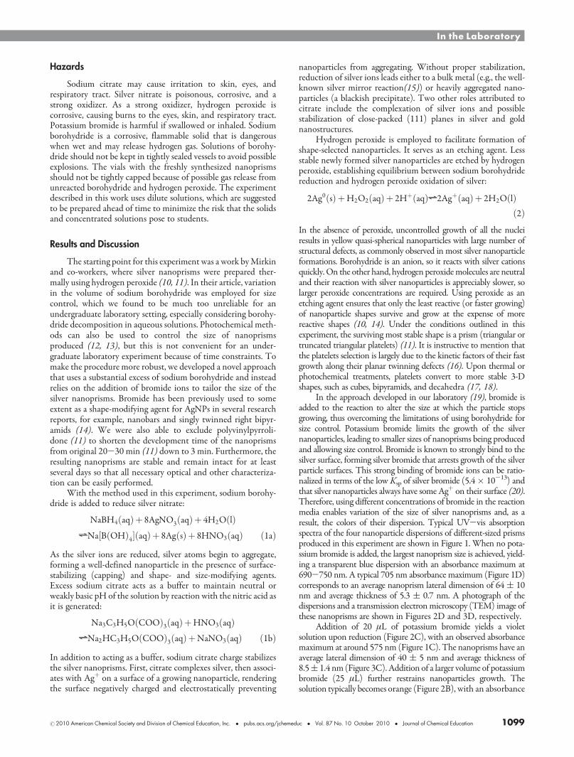
In the approach developed in our laboratory (19), bromide isadded to the reaction to alter the size at which the particle stopsgrowing, thus overcoming the limitations of using borohydride forsize control. Potassium bromide limits the growth of the silvernanoparticles, leading to smaller sizes of nanoprisms being producedand allowing size control. Bromide is known to strongly bind to thesilver surface, forming silver bromide that arrests growth of the silverparticle surfaces. This strong binding of bromide ions can be ratio-nalized in terms of the low Ksp of silver bromide (5.4 10-13) andthat silver nanoparticles always have some Agþ on their surface (20).Therefore, using different concentrations of bromide in the reactionmedia enables variation of the size of silver nanoprisms and, as aresult, the colors of their dispersion. Typical UV-vis absorptionspectra of the four nanoparticle dispersions of different-sized prismsproduced in this experiment are shown in Figure 1. When no pota-ssium bromide is added, the largest nanoprism size is achieved, yield-ing a transparent blue dispersion with an absorbance maximum at690-750 nm. A typical 705 nm absorbance maximum (Figure 1D)corresponds to an average nanoprism lateral dimension of 64( 10nm and average thickness of 5.3 ( 0.7 nm. A photograph of thedispersions and a transmission electronmicroscopy (TEM) image ofthese nanoprisms are shown in Figures 2D and 3D, respectively.
Addition of 20 μL of potassium bromide yields a violetsolution upon reduction (Figure 2C), with an observed absorbancemaximum at around 575 nm (Figure 1C). The nanoprisms have anaverage lateral dimension of 40 ( 5 nm and average thickness of8.5( 1.4 nm (Figure 3C). Addition of a larger volume of potassiumbromide (25 μL) further restrains nanoparticles growth. Thesolution typically becomes orange (Figure 2B), with an absorbance
1100 Journal of Chemical Education
_Vol. 87 No. 10 October 2010
_pubs.acs.org/jchemeduc
_r2010 American Chemical Society and Division of Chemical Education, Inc.
In the Laboratory
maximum of around 470 nm (Figure 1B) and average lateralprism dimension of 35( 4 nm (Figure 3B). Finally, when 40 μLof potassium bromide is used, the nanoprisms virtually do not
develop, resulting in fairly isotropic AgNP shapes, so that ayellow solution typical for quasispherical silver particles can beobserved (Figure 2A). The absorbance maximum is around400-420 nm (Figure 1A). The particles are polydisperse withthe sizes ranging from typical 10 nm up to 30 nm (Figure 3A).
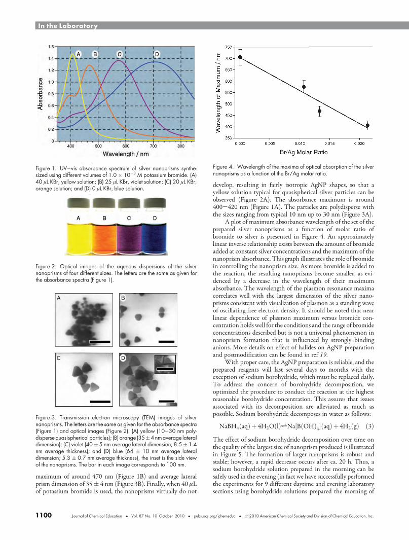
A plot of maximum absorbance wavelength of the set of theprepared silver nanoprisms as a function of molar ratio ofbromide to silver is presented in Figure 4. An approximatelylinear inverse relationship exists between the amount of bromideadded at constant silver concentrations and the maximum of thenanoprism absorbance. This graph illustrates the role of bromidein controlling the nanoprism size. As more bromide is added tothe reaction, the resulting nanoprisms become smaller, as evi-denced by a decrease in the wavelength of their maximumabsorbance. The wavelength of the plasmon resonance maximacorrelates well with the largest dimension of the silver nano-prisms consistent with visualization of plasmon as a standing waveof oscillating free electron density. It should be noted that nearlinear dependence of plasmon maximum versus bromide con-centration holds well for the conditions and the range of bromideconcentrations described but is not a universal phenomenon innanoprism formation that is influenced by strongly bindinganions. More details on effect of halides on AgNP preparationand postmodification can be found in ref 19.
With proper care, the AgNP preparation is reliable, and theprepared reagents will last several days to months with theexception of sodium borohydride, which must be replaced daily.To address the concern of borohydride decomposition, weoptimized the procedure to conduct the reaction at the highestreasonable borohydride concentration. This assures that issuesassociated with its decomposition are alleviated as much aspossible. Sodium borohydride decomposes in water as follows:
NaBH4ðaqÞþ 4H2OðlÞhNa½BðOHÞ4ðaqÞþ 4H2ðgÞ ð3ÞThe effect of sodium borohydride decomposition over time onthe quality of the largest size of nanoprism produced is illustratedin Figure 5. The formation of larger nanoprisms is robust andstable; however, a rapid decrease occurs after ca. 20 h. Thus, asodium borohydride solution prepared in the morning can besafely used in the evening (in fact we have successfully performedthe experiments for 9 different daytime and evening laboratorysections using borohydride solutions prepared the morning of
Figure 2. Optical images of the aqueous dispersions of the silvernanoprisms of four different sizes. The letters are the same as given forthe absorbance spectra (Figure 1).
Figure 1. UV-vis absorbance spectrum of silver nanoprisms synthe-sized using different volumes of 1.0 10-3 M potassium bromide. (A)40 μL KBr, yellow solution; (B) 25 μL KBr, violet solution; (C) 20 μL KBr,orange solution; and (D) 0 μL KBr, blue solution.
Figure 3. Transmission electron microscopy (TEM) images of silvernanoprisms. The letters are the same as given for the absorbance spectra(Figure 1) and optical images (Figure 2). (A) yellow (10-30 nm poly-disperse quasispherical particles); (B) orange (35(4nmaverage lateraldimension); (C) violet (40( 5 nm average lateral dimension; 8.5( 1.4nm average thickness); and (D) blue (64 ( 10 nm average lateraldimension; 5.3 ( 0.7 nm average thickness), the inset is the side viewof the nanoprisms. The bar in each image corresponds to 100 nm.
Figure 4. Wavelength of the maxima of optical absorption of the silvernanoprisms as a function of the Br/Ag molar ratio.

r2010 American Chemical Society and Division of Chemical Education, Inc.
_pubs.acs.org/jchemeduc
_Vol. 87 No. 10 October 2010
_Journal of Chemical Education 1101
In the Laboratory
the experiment). Borohydride solutions still have to be preparedon a daily basis, because using old borohydride will not achievereduction necessary to produce larger nanoprisms.
Important Observations for Successfully Conducting theExperiment
The volume of potassium bromide added to the solutionproved to be critical. Some first-year students may need to besupervised on use of micropipets, which was successfully doneby properly trained teaching assistants. The most commonstudent mistake is to press the micropipet button all the wayin when drawing up the solution, which leads to dispensinglarger volumes of bromide and results in yellow nanoparti-cle solutions produced in all the vials where bromide wasadded. Despite all the pitfalls of usually sensitive nanoparticlepreparations, the overall rate of the student success in produc-ing more than three solutions of different colors was betterthan 85%.
For the Beer's law experiment, if high purity distilled water isnot used, larger nanoprisms may quickly fragment into smallerparticles resulting in a characteristic yellow solution regardless ofthe starting shape and size. To overcome this issue, high-qualityreverse osmosis water or better must be used for all aspects of theexperiment.
Finally, this experiment has been successfully introduced in2009 in an introductory university chemistry class, with 500þstudents (groups of 20-24 students working in pairs) success-fully performing it to date. The students found the experiment tobe fairly challenging, yet rewarding.
Conclusion
The experiment described herein presents a simple, effectivemethod for undergraduate students to synthesize and character-ize silver nanoprisms of different colors within a 3-h laboratory.The colors of the dispersions are due to size-dependence of
the plasmon resonance of AgNPs. As a result, students areintroduced to nanochemistry and nanoscience in a manner thatis readily perceived and understood. In first-year laboratorysettings, the proposed experiment can nicely reinforce conceptsof colorimetry, UV-vis spectroscopy, and Beer's law. In moreadvanced laboratories, measurements by scanning probe micro-scopy, light scattering, electron microscopy, and so forth can beperformed based on the proposed synthetic procedures.
Acknowledgment
The authors gratefully acknowledge financial support by theNatural Science and Engineering Research Council of Canadaand Research Corporation for Science Advancement. TheCentre for Nanostructure Imaging, University of Toronto isgreatly appreciated for access to Electron Microscopy facilities.
Literature Cited
1. Xia, Y.; Xiong, Y.; Lim, B.; Skrabalak, S. E. Angew. Chem., Int. Ed.2009, 48, 60.
2. Winkelmann, K.; Noviello, T.; Brooks, S. J. Chem. Educ. 2007, 84,709.
3. Boatman, E.M.; Lisensky, G. C.;Nordell, K. J. J. Chem. Educ. 2005,82, 949.
4. Keating, C. D.; Musick., M. D.; Keefe, M. H.; Natan, M. J. J. Chem.Educ. 1999, 76, 949.
5. McFarland, A. D.; Haynes, C. L.; Mirkin, C. A.; Van Duyne, R. P.;Godwin, H. A. J. Chem. Educ. 2004, 81, 544A.
6. Solomon, S. D.; Bahadory, M.; Jeyarajasingam, A. V.; Rutkowsky,S. A. J. Chem. Educ. 2007, 84, 322.
7. Campbell, D. J.; Xia, Y. J. Chem. Educ. 2007, 84, 91.8. Liz-Marzan, L. M. Mater. Today 2004, 7, 26.9. Sun, Y.; Xia, Y. Analyst 2003, 128, 686.
10. Millstone, J. E.; Hurst, S. J.; Metraux, G. S.; Cutler, J. I.; Mirkin,C. A. Small 2009, 5, 464.
11. Metraux, G. S.; Mirkin, C. A. Adv. Mater. 2005, 17, 412.12. Jin, R.; Cao, Y.; Mirkin, C. A.; Kelly, K. L.; Schatz, G. C.; Zheng,
J. G. Science 2001, 294, 1901.13. Jin, R.; Cao, Y.; Hao, E.;Metraux, G. S.; Schatz, G. C.;Mirkin, C. A.
Nature 2003, 425, 487.14. Wiley, B.; Sun, Y.; Xia, Y. Acc. Chem. Res. 2007, 40, 1067.15. Kemp, M. J. Chem. Educ. 1981, 58, 655.16. Aherne, D.; Ledwith, D. M.; Gara, M.; Kelly, J. M. Adv. Funct.
Mater. 2008, 18, 2005.17. McEachran, M.; Kitaev, V. Chem. Commun. 2008, 44, 5737.18. Pietrobon, B.; Kitaev, V. Chem. Mater. 2008, 20, 5186.19. Cathcart, N.; Frank, A. J.; Kitaev, V. Chem. Commun. 2009, 46,
7170–7172.20. Xiong, Y.; Washio, I.; Chen, J.; Sadilek, M.; Xia, Y. Angew. Chem.,
Int. Ed. 2007, 46, 4917.
Supporting Information Available
Description of the experimental procedure; preparation of materi-als provided to students; instructor notes; results of a typical student lab;CAS registry numbers. This material is available via the Internet athttp://pubs.acs.org.
Figure 5. Effect of the decomposition of sodium borohydride on effec-tiveness of the silver nanoprism preparation. Absorption maximum of theblue silver nanoprisms at 650-700 nm region is plotted against theaging time of borohydride solution used for the reduction.

Synthesis of Inverse Opal Photonic Crystals http://mrsec.wisc.edu/Edetc/nanolab/photonic/index4.html
1 of 4 6/2/11 4:34 PM

Synthesis of Inverse Opal Photonic CrystalsProcedure modified by George Lisensky and Jacob Horger, Beloit College, from the Inverse Opal Photonic Crystals Laboratory Guide by R.Schroden and N. Balakrishnan, University of Minnesota MRSEC, 2001.
A sol-gel synthesis using tetraethylorthosilicate and close-packed polymethylmethacrylate spheres as a template yields adimensionally ordered porous silica solid.
Clicking a thumbnail on this web page (http://mrsec.wisc.edu/Edetc/nanolab/photonic/index4.html) shows a movie of that step.
ProcedureWear eye protection Chemical gloves
recommendedFumehood recommended
Use ethanol to wet a filter paper in a small Buchner funnel connected to awater aspirator.
Place 2.0 gram of dry polymethacrylate spheres in the funnel and spreadthem out to evenly cover the entire filter. Turn on the water aspirator andslowly wet the entire surface with a well mixed solution of 2.0 mL 100%ethanol, 3.0 mL tetraethylorthosilicate, 1.5 mL pure water, and 0.5 mL conchydrochloric acid. Try to wet all the spheres before running out of liquid, butif not all of the polymethylmethacrylate is coated the yield will simply besmaller. On the other hand, once all the spheres are wet, stop adding liquid
or the product may be too dense. Aspirate for 20 minutes to speed drying.
Transfer the product to combustion boats.
Place the combustion boats into the quartz liner of a tube furnace (or a ventilated box furnace) in ahood. Ramp the temperature at 2 degrees C/minute from room temperature to 300 degrees C tocomplete the silica formation. Hold at 300 degrees C for 2 hours. Ramp the temperature at 2degrees C/minute to 550 degrees C to decompose the polymethylmethacrylate spheres. Hold at550 degrees C overnight (ten hours). Cool the oven to room temperature.
Synthesis of Inverse Opal Photonic Crystals http://mrsec.wisc.edu/Edetc/nanolab/photonic/index4.html
2 of 4 6/2/11 4:34 PM

High quality samples will be apparent by their opalescence.
Properties
What color is your product in air? (The index of refraction of silica is 1.460 and of air is 1.000)Add a drop of ethanol to a small portion of your product. What color do you observe? (The index of refraction of ethanol is1.360)Add a drop of toluene to a small portion of your product. What color do you observe? (The index of refraction of toluene is1.496)Based on the sphere size used as a template, predict the absorption wavelength for each of these. How do you need tomodify the equation for closed-packed spheres for the inverse material?
Characterization with a Scanning Electron Microscope
Samples are deposited on conducting graphite tape and gold coated.
The coated samples are placed into an electron microscope.
Zooming in on a sample of monodispersed polymethylmethacrylate spheres. What is the diameterof the spheres?Larger movie in a new window
Zooming in on a sample of monodispersed polymethylmethacrylate spheres. What is the diameterof the spheres?Larger movie in a new window
Zooming in on a sample of inverse opal photonic silica crystal. What is the diameter of the holes?Larger movie in a new window
Flying over the surface of a sample of inverse opal photonic crystal (2000x magnification.)
Materials
polymethacrylate spheres100% ethanolconc hydrochloric acidtetraethylorthosilicate
combustion boats
Synthesis of Inverse Opal Photonic Crystals http://mrsec.wisc.edu/Edetc/nanolab/photonic/index4.html
3 of 4 6/2/11 4:34 PM

tube furnace
Exploring the Nanoworld | MRSEC Nanostructured InterfacesCopyright © 2008 The Board of Regents of the University of Wisconsin System.
This page created by George Lisensky, Beloit College. Last modified March 11, 2011 .
Synthesis of Inverse Opal Photonic Crystals http://mrsec.wisc.edu/Edetc/nanolab/photonic/index4.html
4 of 4 6/2/11 4:34 PM

In the Laboratory
www.JCE.DivCHED.org • Vol. 82 No. 5 May 2005 • Journal of Chemical Education 765
Nanotechnology, the study of materials having at leastone dimension smaller than 100 nm, is a rapidly progressingfield. Commercialization of nanotechnology using nanoscaleparticles can already be found in applications ranging fromenhanced fabrics (1) to self-cleaning windows (2). Chemis-try plays a central role in the development of nanoscale ma-terials because it gives precise control over the compositionof the nanostructures.
Despite the emerging emphasis on nanotechnology bythe media, funding agencies, and academic and industrial re-search programs, its entry into the high school and collegechemistry curricula has been slow (3). There is little oppor-tunity in most undergraduate chemistry courses for studentsto prepare nanoscale materials and explore how these mate-rials will be used in the technologies of the future. Experi-ments described in this Journal allow students to synthesize
nanocrystalline Eu-doped yttria (4), watch the exciting be-havior of a ferrofluid containing nanoparticles of magnetite(5), study the self-assembly of a monolayer of gold nanopar-ticles (6), and create their own carbon nanotubes (7). Theexperiment described in this article involves a fascinating areaof current nanotechnology research: the synthesis and studyof the properties of wires that are nanometers wide and mi-crometers long.
Nanowires are an intensively studied area of researchowing to their potential applications in nanoscale electronic,magnetic, optical, and mechanical devices. One common ap-proach to forming nanowires is the template synthesis tech-nique, which was first popularized more than ten years agoand has become widely used (8, 9). Nanoporous alumina orpolycarbonate membranes are used as templates to direct thegrowth of nanowires. Generally, a membrane’s pores are filledwith one or more metals via a technique such as electrodepo-sition. The membrane can be chemically removed, leavingmetallic nanowires behind. A schematic description of theprocess is shown in Figure 1. The technique has been adaptedto synthesize nanoscale semiconductor oxides (10), supercon-ductors (11), magnetic structures (12), and giant magnetore-sistance materials (13). Nickel nanowires are of particularinterest to researchers because they could be employed to in-crease magnetic storage density (14). We present a straight-forward electrochemical method to create nickel nanowiresusing an AA battery and observe them with an optical mi-croscope.
A general problem with using nanowires in devices isthe ability to control their position. Recently nickel nanowireshave been manipulated using magnetic fields (15). In thisexperiment, students can watch the movement and alignmentof their nickel nanowires through the lens of an opticalmicroscope as they use common magnets to alter the appliedmagnetic field.
This experiment is an inexpensive, easy-to-understandintroduction to nanowire synthesis. It especially highlightsthe role electrochemistry plays in the fabrication of nanoscalestructures. The experiment is appropriate for introductoryand advanced undergraduate chemistry students and couldbe used in the curriculum when redox chemistry, electro-chemistry, materials chemistry, or magnetism are discussed.
Template Synthesis and Magnetic Manipulation Wof Nickel NanowiresAnne K. Bentley, Mohammed Farhoud, and Arthur B. EllisDepartment of Chemistry, University of Wisconsin–Madison, Madison, WI 53706
George C. Lisensky*Department of Chemistry, Beloit College, Beloit, WI 53511; *[email protected]
Anne-Marie L. NickelDepartment of Physics and Chemistry, Milwaukee School of Engineering, Milwaukee, WI 53202
Wendy C. Crone**Department of Engineering Physics, University of Wisconsin–Madison, Madison, WI 53706; **[email protected]
Figure 1. Schematic description of the template synthesis technique.
add a conductive coating to a porous alumina membrane
electrodepositnickel
remove coating anddissolve alumina

In the Laboratory
766 Journal of Chemical Education • Vol. 82 No. 5 May 2005 • www.JCE.DivCHED.org
Experimental Procedure
The alumina membranes are available commercially fromWhatman, Inc. (Detailed lab instructions and informationon supplies can be found in the Supplemental Material.W)One side of the alumina membrane is first sputtered withsilver metal or painted with GaIn eutectic to block the poresand form a conductive layer that serves as the cathode. Themembrane is mounted on a copper plate using insulating elec-trical tape. The tape covers the copper plate and prevents thenickel from electrodepositing on it. The assembly is placedin a 50-mL beaker, a nickel wire is added as the anode, andboth electrodes are connected to an AA battery. Adding com-mercial Ni plating solution (available from Technic, Inc.)completes the circuit and Ni2+ is reduced to Ni inside thepores of the membrane while the Ni wire is oxidized to Ni2+.The plating solution can be reused many times. The batteryprovides a potential of 1.5 V, which is well negative of nickel’sstandard reduction potential of 0.257 V. The electrochemi-cal setup is shown in Figure 2.
The electrodeposition is allowed to continue for 10–50minutes, depending on the length of wires desired. The mem-brane is removed from the copper plate, the Ag metal or GaIneutectic is dissolved using concentrated nitric acid, and thealumina is dissolved using 6 M sodium hydroxide. As thealumina dissolves, the nanowires are liberated and float freelyin the sodium hydroxide solution. A series of washing stepsdilutes the base and the nanowires can be suspended in anumber of solvents indefinitely for storage.
Hazards
This experiment requires the handling of concentratednitric acid and 6 M sodium hydroxide. Both will burn skinand eyes. Exposure to nickel (through skin or oral absorp-tion) can cause skin rashes. GaIn eutectic may cause skin ir-ritation. The hazards of nickel nanowires due to inhalationare unknown, so nanowires should be kept and handled insolution. Goggles must be worn at all times during the prepa-ration of the nanowires and gloves must be worn when han-dling the GaIn eutectic, nickel solution, and strong acids andbases.
Results and Discussion
Magnetic ManipulationTo test the magnetic response of the liberated nickel
nanowires, set a magnet at the side of a vial containing thenanowire suspension and allow it to sit for a few minutes.Spikes in the nanowire material will become visible. Thesespikes follow the magnetic field lines similar to the behaviorobserved in ferrofluid (5). This effect can be seen in Figure 3.
To observe the magnetic response of individual nano-wires, place one drop of nanowire suspension on a cleanmicroscope slide and cover with a cover slip. (The nanowirescan be suspended in water or ethylene glycol.) Place the slideon the stage of an optical microscope. Wires can be seen withas little as 10× magnification. By holding a rectangularmagnet on one side of the microscope slide while examiningthe nanowires, students can align the nanowires with themagnetic field. Nanowires can be aligned horizontally orvertically as shown in Figure 4. Additionally, if a magnet isspun on one side of the slide, the nanowires will spin likesmall stir bars. Movies of the magnetic behavior of thenanowires are included as part of the Supplemental MaterialW
and online video lab manual (16).To examine the nanowires using a scanning electron mi-
croscope (SEM), a drop of water containing the nanowiresis allowed to dry. Samples of nanowires imaged using a LEO1530 FE-SEM are shown in Figure 5. If a magnetic field isapplied to the drop as it dries, the nanowires will align alongthe direction of the magnetic field, as shown in Figure 5B.
Length of Nanowires versus Deposition TimeA variation of the synthesis is to assign different deposi-
tion times to groups of students and use SEM to measure theaverage length of nanowires produced by each pair of students.Data compiled by students at UW–Madison and Beloit Col-lege using GaIn eutectic as the cathode are shown in Figure6. As expected, longer deposition times produce longer nanow-ires. The nanowires grow at a rate of approximately 1 µmminunder the laboratory conditions described; no special effortwas made to control the experimental geometry. Nanowiresformed using the sputtered silver cathode grew approximatelytwice as fast as those formed using the GaIn eutectic cathode.
Figure 3. The nanowires in ethylene glycol respond to a cow mag-net set at one side of the vial.
Figure 2. The electrochemical cell showing the membrane taped toa copper plate as the cathode, the nickel wire as the anode, theNi plating solution, and an AA battery.

In the Laboratory
www.JCE.DivCHED.org • Vol. 82 No. 5 May 2005 • Journal of Chemical Education 767
X-Ray DiffractionX-ray powder diffraction patterns of the nanowires taken
both before and after the nanowires are liberated from themembrane are shown in Figure 7. While the wires are stillembedded in the membrane, the nickel(220) peak is mostintense. This implies that the nanowires are growing with apreferential orientation of the (220) plane in the directionof growth. After the wires are liberated and dispersed ran-domly on a microscope slide, the XRD intensities closelymatch the Ni standard pattern.
Use and Assessment
The lab has been included in courses at the Universityof Wisconsin–Madison, Milwaukee School of Engineering,and Beloit College. Students have ranged in background fromfirst-year nonmajors enrolled in a colloquium course on nano-technology to materials science and physics graduate students.Students usually work in pairs to create the nanowires. Thenanowire synthesis takes approximately 90 minutes to com-plete if less than 30 minutes are used for deposition; the re-maining time is used for experiments with the nanowires.Alternatively, the laboratory can be divided into two shorterlab periods. Following the written procedure (available in theSupplemental MaterialW), 23 of 24 pairs of students were suc-cessful in making and observing nickel nanowires. Some
Figure 4. Optical microscope images (20x magnification) of thenanowires aligning horizontally (top) and vertically (bottom).
Figure 5. SEM images of (A) a random arrangement of nanowires;(B) nanowires aligned using a magnet as the drop dried; and (C)upright nanowires on the silver backing after dissolving only thealumina membrane.
courses used an online video lab manual instead of the writ-ten procedure, which provided videos of each step in the ex-periment alongside simplified written instructions (16).Seventeen of nineteen lab teams using the Web-based videolab manual were successful.
Students were asked for their comments regarding boththe clarity of the written or online instructions and the ef-fectiveness a of the lab a teaching tool for the topics of elec-trochemistry and nanotechnology. Most students said theyhad never heard of nanotechnology or nanowires before thelab. The “downtime” during nanowire deposition was oftenused for a brief introductory lecture about nanoscale materi-als. Students reported that this lecture was helpful in theirunderstanding of the lab. In addition to appreciating the

In the Laboratory
768 Journal of Chemical Education • Vol. 82 No. 5 May 2005 • www.JCE.DivCHED.org
nearly 100% success rate of the lab, the students liked therelevance to current research and emerging technologies. Onestudent said, “I felt like I was contributing to science andnot just doing a lab that’s been done a thousand times.” An-other said the lab demonstrated that “it isn’t that hard to makenanowires.” Many enjoyed seeing their nanowires using theoptical microscope: “It was neat because we got a visible prod-uct that has potential technological uses in the world.”
Conclusion
This experiment gives students a unique opportunity tocreate and manipulate their own nanoscale materials. It bringsnanotechnology into the teaching lab and shows students howelectrochemistry can be used to make nanoscale structures.The lab is applicable across the undergraduate curriculum(from general chemistry to engineering to materials science)and may also be appropriate for high school chemistrycourses.
Acknowledgments
Funding for the development of this lab experimentcame from the National Science Foundation Materials Re-search Science and Engineering Center (MRSEC) on Nano-structured Materials and Interfaces (award #DMR-0079983).The work was also supported by an NSF Graduate ResearchFellowship (AKB). We thank Karen Nordell (Lawrence Uni-versity), Eric Voss (Southern Illinois University Edwardsville),Donald Stone (Materials Science, UW–Madison), FranzHimpsel (Physics, UW–Madison), John Moore (Chemistry,UW–Madison), Gordon Bain (Chemistry, UW–Madison),and our students for their assistance with testing the lab andsuggestions for improvements in the procedure.
WSupplemental Material
Instructions for the students, including lab questions,notes for the instructor and videos of the magnetic behaviorare available in this issue of JCE Online.
Literature Cited
1. Nano-Tex. http://www.nano-tex.com (accessed Feb 2005).2. PPG SunClean Self-Cleaning Glass. http://www.ppg.com/
gls_residential/gls_sunclean (accessed Feb 2005).3. National Nanotechnology Initiative. http://www.nano.gov (ac-
cessed Feb 2005).4. Bolstad, D. B.; Diaz, A. L. J. Chem. Educ. 2002, 79, 1101–
1104.5. Berger, P.; Adelman, N. B.; Beckman, K. J.; Campbell, D. J.;
Ellis, A. B.; Lisensky, G. C. J. Chem. Educ. 1999, 76, 943–948.
6. Keating, C. D.; Musick, M. D.; Keefe, M. H.; Natan, M. J.J. Chem. Educ. 1999, 76, 949–955.
7. Fahlman, B. D. J. Chem. Educ. 2002, 79, 203–206.8. Penner, R. M.; Martin, C. R. Anal. Chem. 1987, 59, 2625–
2630.9. Hulteen, J. C.; Martin, C. R. J. Mater. Chem. 1997, 7, 1075–
1087.10. Lakshmi, B. B.; Patrissi, C. J.; Martin, C. R. Chem. Mater.
1997, 9, 2544–2550.11. Yi, G.; Schwarzacher, W. Appl. Phys. Lett. 1999, 74, 1746–
1748.12. AlMawlawi, D.; Coombs, N.; Moskovits, M. J. Appl. Phys.
1991, 70, 4421–4425.13. Evans, P. R.; Yi, G.; Schwarzacher, W. Appl. Phys. Lett. 2000,
76, 481–483.14. Pignard, S.; Goglio, G.; Radulescu, A.; Piraux, L.; Dubois,
S.; Declemy, A.; Duvail, J. L. J. Appl. Phys. 2000, 87, 824–829.
15. Tanase, M.; Bauer, L. A.; Hultgren, A.; Silevitch, D. M.; Sun,L.; Reich, D. H.; Searson, P. C.; Meyer, G. J. Nano Lett. 2001,1, 155–158. Bentley, A. K.; Trethewey, J. S.; Ellis, A. B.; Crone,W. C. Nano Lett. 2004, 4, 487–490.
16. Nickel Nanowires. http://mrsec.wisc.edu/edetc/nanolab/nickel/index.html (accessed Feb 2005).
Editor’s Note
For more information about electrochemical fabrication ofnanowires, see pp 720–726 in this issue.
Figure 6. The relationship between nickel deposition time and lengthof the nanowires recovered from the membrane. Triangles repre-sent data from UW–Madison and circles represent data from BeloitCollege.
Deposition Time / min
Nan
owire
Len
gth
/ µm
60
50
40
30
20
10
00 10 20 30 40 50 60 70
Figure 7. X-ray powder diffraction pattern of (A) nanowires stillembedded in the alumina membrane, (B) liberated nanowires dis-persed on a microscope slide, and (C) the JCPDS standard file #4-850 for nickel.
A
B
C
(111) (200)
(220)
(311)
(222)
2θ / deg
Inte
nsity
40 50 60 70 80 90 100 110