novel vlsi design & verification strategies for advanced wireless technologies
TRANSCRIPT

Novel VLSI Design & Verification Strategies forAdvanced Wireless Technologies

© 2015, HCL Technologies. Reproduction Prohibited. This document is protected under Copyright by the Author, all rights reserved.
Abstract
Abbreviations
Market trend/ Challenges
Solution
Best Practices
Common Issues
ConclusionConclusion
Reference
Author Info
3
3
4
4
9
9
99
10
10
Table of Contents
© 2015, HCL Technologies. Reproduction Prohibited. This document is protected under Copyright by the Author, all rights reserved.
Recently there has been an increase in the usage of VLSI solutions like FPGA/ASIC in wireless systems, replac-ing the earlier used DSP processors. Now most of the Layer 1 - PHY Layer is getting done in FPGA to meet the high bandwidth/throughput requirements. This is because DSPs available in the market are not able to meet the complexity and timing. Also the only choice for Digital IF Processing Function is FPGAs since high sampling rate processing is not possible in DSPs. In this whitepaper, we propose novel VLSI design and verification strategies for 4G LTE /5G LTE-A wireless technologies to meet the challenges like time-to-market in emerging wireless market in the telecom vertical.
Sl.No
1
2
3
4
5
6
77
8
9
10
11
12
13
1414
15
16
17
18
VLSI
FPGA
ASIC
DSP
LTE
LTE-ALTE-A
OFDMA
MIMO
FFT/iFFT
FEC
SV
Digital IF
BFMBFM
GMAC
RTL
TTI
BTS
IO
Very Large Scale Integration
Field Programmable Gate Array
Application Specific Integrated Circuit
Digital Signal Processors/Processing
Long Term Evolution
LTE- AdvancedLTE- Advanced
Orthogonal Frequency Division Multiple Access
Multiple Input Multiple Output
Fast Fourier Transform/Inverse Fast Fourier Transform
Forward Error Correction
System Verilog
Digital intermediate frequency
Bus Functional ModelBus Functional Model
Giga Multiply Accumulates
Register Transfer Level
Transmission Time Interval
Base transceiver station
Input and Output
Full FormAcronyms
Abstract
Abbreviations
Novel VLSI Design & Verification Strategies for Advanced Wireless Technologies | 3
© 2015, HCL Technologies. Reproduction Prohibited. This document is protected under Copyright by the Author, all rights reserved.
VLSI solutions like FPGA/ASIC continue to gain momentum by fast replacing the earlier DSP processors in wireless systems. This is because high-end FPGAs support a large number of embedded DSP blocks leading to operations at GMACs whose order of magnitude are greater than the performance of DSPs available in the market. The current leading FPGA vendors are Xilinx and Altera. For example, Altera - Stratix V GS (5SGSD8) series have 695K Logic Elements, 1050K Registers, 2567 – M20K Memory Blocks and variable precision DSP blocks supporting up to 3,926- 18x18 multipliers which is equivalent to 1,963 DSP Blocks. With this, we can configureconfigure to natively support signal processing with precision range from 9x9 to 36x36 including float-ing-point implementations [1]. Xilinx – Vertex 7 series have 2 million logic gates, 85Mb block RAM and 3,600 DSP blocks [2].
Also, most of the Layer 1 - PHY Layer is getting done in FPGA due to the inability of the available DSPs to meet the high bandwidth/throughput requirements. FPGAs are more suitable for Digital IF Processing Function as well since the high sampling rate processing is not well supported by the DSPs. This whitepaper proposes novel VLSI design and verification strategies for 4G LTE /5G LTE-A wireless technologies to meet the challenges like time to market in emerging wireless market in telecom vertical.
Time to market is a key parameter which determines the success of 4G LTE/5G LTE-Advanced wireless tech-nologies systems due to demanding market compulsions like short life-span of smart phones, tablets and other devices which use these wireless technologies. These wireless technologies are based on MIMO-OFDMA system[3] and optimal HW/SW partitioning for such MIMO-OFDMA system[4]. The HW portion of MIMO-OFDMA needs to be implemented on FPGA/ASICs using VLSI design, development and verification techniques. The gate complexity of these designs is very high of the order of 10 Million gates. In this whitepaper, we propose somesome novel VLSI design & verification strategies to meet the time to market requirement for such high com-plexity MIMO-OFDMA based next generation wireless systems as listed below.
Adopting system level design methodology, instead of behavioral level design methodology to develop FPGA prototype (proto)
Adopting advanced verification techniques in Pre-Silicon (Pre-Si) verification instead of simple File I/O based technique
FPGA prototyping in parallel to ASIC development
Post-silicon validation on FPGA proto in parallel to Pre-Si verification
Market trend/ Challenges
Solution
Novel VLSI Design & Verification Strategies for Advanced Wireless Technologies | 4

© 2015, HCL Technologies. Reproduction Prohibited. This document is protected under Copyright by the Author, all rights reserved.
The traditional design methodology to implement the digital signal processing (DSP) blocks in FPGA/ASIC is by using behavioral level of RTL coding, which is very time consuming process to develop the DSP blocks. It also requires highly skilled DSP experts and design engineers for implementation. Even this coding methodology actually evolved from, switch level gate level data flow behavioral level abstraction of hardware description language (HDL) development as design complexity became more complex in the order of 10/100/1000/10000 gates respectively. As per the current industry trends, behavioral level of RTL codingcoding used as the gate complexity is more than 10,000 gates which is generally referred to as VLSI design. However, 4G/5G wireless technology necessitates very high design complexity of the order of 10 Million gates, hence to develop these system one more level of abstraction i.e. system level of abstraction is required in terms of time to market, easy to design, verification and validation.
1. System Level Design Methodology
1.1 Traditional Design Methodology
For highly complex systems like Base Stations (BTS) for 4G/5G development system, before going to the ASIC chipset development, FPGA prototyping is necessary for proof of concept. Current leading FPGA vendors, both Xilinx and Altera, provide a platform for system level design.
Altera-Altera- Qsys & Megacore GUI tool[1], have DSP & IO interface function like FFT/iFFT, FEC blocks, Filters, CPRI, Ethernet, DMA, RAM/ROM, FIFO, Arbiter, SerDes, PLL etc. Basically all the system design components are available in the Altera tool itself and these components are easily interconnected with Altera property interface like Avalon® – ST (streaming) and MM (Memory Mapped) interface. By properly configuring and interfacing these readymade blocks (GUI based drag and drop) in Qsys design system console, we can easily build our own system and this kind of design methodology is referred as system level design meth-odology.odology. Some DSP blocks like Turbo/LDPC decoders may not be available in the Altera-Qsys library, for this block we can generate the design and test bench HDL code output from MATLAB HDL Coder™ tool which needs to be used in conjunction with MATLAB Simulink tool. We can manually write the HDL wrapper and integrate with Qsys component which is very less time consuming process.
Xilinx- Vivado™[2], design suite provides the complete SOC design platform. Most of the system design modules are available in the Xilinx SmartCore™ and LogiCORE™ IP tool itself. RTL code of DSP blocks like turbo encoder/decoder can be generated from the Vivado High- Level Synthesis (HLS) tool, which converts the C/C++/System C design to RTL design. Even though the RTL code obtained from the tool, it will be better optimized than hand written HDL code. Vivado IP Integrator tool provides GUI based plug and play components which is interconnected by AXI interface, apart from that FPGA itself have the ARM processor which will provide more elegant solutions.
1.2 System Level Design Methodology
Novel VLSI Design & Verification Strategies for Advanced Wireless Technologies | 5
© 2015, HCL Technologies. Reproduction Prohibited. This document is protected under Copyright by the Author, all rights reserved.
The benefits of system level design methodology are:
Hence the system level design methodology is well predictable and the best engineering approach for highly complex systems like 4G/5G technologies as the above benefits lead to quick time to market solu-tions.
Reduction in the design cycle time drastically
Reduction in the design engineer head count
These blocks are verified and validated, hence low risk
Quick FPGA prototyping, which is proof of concept for any new system design idea/approach.
Low cost product
2. Advanced Pre-Si Verification Strategies
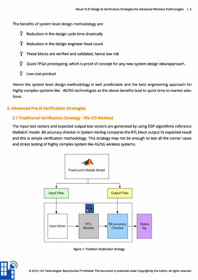
The input test vectors and expected output test vectors are generated by using DSP algorithms reference Matlab/C model. Bit accuracy checker in System Verilog compares the RTL block output Vs expected result and this is simple verification methodology. This strategy may not be enough to test all the corner cases and stress testing of highly complex system like 4G/5G wireless systems.
Figure 1: Tradition Verification Strategy
2.1 Traditional Verification Strategy - File I/O Method
Novel VLSI Design & Verification Strategies for Advanced Wireless Technologies | 6

© 2015, HCL Technologies. Reproduction Prohibited. This document is protected under Copyright by the Author, all rights reserved.
In this strategy C model of the DSP algorithm needs to be integrated with System Verilog by using DPI (Direct Programming Interface) technique or the MATLAB model of the DSP algorithm needs to be inte-grated with EDA simulator link tool. With this methodology, we can generate the test vector on the fly and we can perform the constrained random unit/integration/regression verification more efficiently. We can also verify the magnitude and phase plots against the MATLAB model automatically. As part of the regres-sion verification for filters, functional testing is done with the following type of input vectors, impulse (for latency and group delay), sine, step for gain, multi tone and random vectors.
Figure 2: Advanced Verification Strategy
2.2 Advanced Verification Strategy using C/MATLAB reference model
FPGA prototype platform is proof of concept for the idea and it is useful for functional validation however with lower/reduced throughput level since FPGA design runs at lower clock frequency compared to ASIC. The advantages of FPGA proto-typing are:
DUT
Checker(SV)
Test InputGeneration(SV)
SV Wrapper (DP)
C Code
Real Time Workshop(Matlab to C conversion)
(Embedded) MatlabFixed Point ToolboxSignal Processing
Toolbox
System Verilog Test Environment
Reference Model(C Code)
3. FPGA Prototyping
Novel VLSI Design & Verification Strategies for Advanced Wireless Technologies | 7

© 2015, HCL Technologies. Reproduction Prohibited. This document is protected under Copyright by the Author, all rights reserved.
FPGA prototyping platform helpful to validate the driver-software.
Real/actual data can be injected into the design, by which we can identify the metastability issues, simulation and synthesis mismatch.
Real Hardware (CPRI and SerDes) can be validated in the FPGA which will bring up the functional model issues, if any.
WeWe can test all possible random pattern test sequence generation in periodic interval (dai-ly/weekly) to validate all the features of the SOC.
Memory size
Functional validation under extreme thermal conditions by intensively heating
Timing and Voltage parameter validation
Signal integrity test to validate the critical signals like reset, clock, control signals, etc.,
ATPG (Automatic Test Pattern Generation) which will inject the test vectors into the chip
Hardware interface test like board diagnostic test-sanity check, powered signal test
Frequency clock margin testFrequency clock margin test
Low Voltage Vs Low/High Temperature test and vice versa
Eye diagram, Timing margin, Rise/Fall time, Jitter, BER– Bit Error Ratio measurement test
Loop back test to validate the protocol like CPRI, Ethernet, etc.
Power on reset test
Noise Immunity test to validate the noise margin
4. Post-Silicon Validation
Post Silicon Validation needs to be performed together by manufacturer and design team. In this method-ology we can test all chip IOs with full throughput, which will verify all the DSP blocks throughput, arbiter speed and bus/bridge functionality. In FPGA proto-typing we will have the limitation of speed which will not be there in post-silicon validation. We can validate the following features in post-silicon validation:
Figure 3: Post Silicon Validation Strategy
Chipset(FPGA/ASIC - SOC)
PC(Windows/Linux Platform)Validation Environment
Test Generation Hardware(Automatic Testing Machine)
Novel VLSI Design & Verification Strategies for Advanced Wireless Technologies | 8

© 2015, HCL Technologies. Reproduction Prohibited. This document is protected under Copyright by the Author, all rights reserved.
Best Practices
Common Issues
Conclusion
When the proposed design and verification strategies are adopted compared to other traditional strate-gies, there will be definite benefits in the following
1. Meeting the timing: It means satisfying the real-time processing requirements specified in the standard which is TTI of 1 ms for LTE.
2. Reliability: Since the proposed strategies ensure reliability by more than one means, like post-silicon validation in addition to pre-si verification, the outcome of these strategies would be highly reliable.
3. Scalability: As the standards evolve more features would get adopted and due to scalable nature of our proposed strategies it can be easily adopted for newer versions of the standards.
4. Time to Market: 4. Time to Market: All the proposed techniques, if used effectively, will get a definite advantage in time to market compared to traditional strategies particularly the parallel post-silicon validation on proto.
Although the proposed strategies have definite benefits, some of the challenges in the proposed solutions may be:
The proposed VLSI design, verification and validation strategy is definitely a good approach for LTE/LTE-A Layer-1 development as compared to the traditional approaches. This solution gives an edge in time to market with the flexibility and rapid prototyping capabilities, which is a critical parameter in 4G LTE/5G LTE-Advanced wireless technologies systems due to the short lifespans of the devices which use them. The proposed strategy also provides additional benefits of meeting the timing, reliability and scalability.
1. Requires a change in mindset of the engineers to adapt the proposed strategies compared to tradi tional strategies
2. Tool cost for adopting some of the proposed strategies is higher compared to traditional strategies
Novel VLSI Design & Verification Strategies for Advanced Wireless Technologies | 9

For more details contact: [email protected] us on twitter: http://twitter.com/hclers andOur blog http://www.hcltech.com/blogs/engineering-and-rd-servicesVisit our website: http://www.hcltech.com/engineering-rd-services
Hello, I’m from HCL’s Engineering and R&D Services. We enable technology led organizations to go to market with innovative products and solutions. We patner with our customers in building world class products and creating associated solution delivery ecosystems to help bring market leadership. We develop engineering products, solutions and platforms across Aerospace and Defense, Automotive, Consumer Electronics, Software, Online, Industrial Manufacturing, Medical Devices, Networking and Telecom, Office Automation, Semiconductor and Servers & Storage for our customers.
This whitepaper is published by HCL Engineering and R&D Services.
The views and opinions in this article are for informational purposes only and should not be considered as a substitute for professional business advice. The use herein of any trademarks is not an assertion of ownership of such trademarks by HCL nor intended to imply any association between HCL and lawful owners of such trademarks.
For more information about HCL Engineering and R&D Services,Please visit http://www.hcltech.com/engineering-rd-services
Copyright@ HCCopyright@ HCL TechnologiesAll rights reserved.
C SaminathanHCL Engineering and R&D Services
G Sangeet HCL Engineering and R&D Services
Dr G V RangarajHCL Engineering and R&D Services
Reference
Author Info
1. Altera FPGA and Tools - http://www.altera.com
2. Xilinx FPGA and Tools - http://www.xilinx.com
3. 3GPP LTE Standards: TS 36.201, TS 36.211 & TS 36.212
http://www.3gpp.org/ftp/Specs/html-info/36201.htm
http://www.3gpp.org/ftp/Specs/html-info/36211.htm
http://www.3gpp.org/ftp/Specs/html-info/36212.htm
4. Altera’s Whitepaper on DSP-FPGA System Partitioning for MIMO-OFDMA Wireless Base stations, October 20074. Altera’s Whitepaper on DSP-FPGA System Partitioning for MIMO-OFDMA Wireless Base stations, October 2007
Adopting the Pairwise Test Design Technique to Optimize Printer Driver Test Coverage | 10