novel terahertz emitters and detectors: ingaas slot diodes...
TRANSCRIPT

Thesis for The Degree of Licentiate of Engineering
Novel Terahertz Emitters and Detectors:InGaAs Slot Diodes and InAs Self-Switching Diodes
Andreas Westlund
Microwave Electronics LaboratoryDepartment of Microtechnology and Nanoscience - MC2
Chalmers University of TechnologyGothenburg, Sweden, 2013
Novel Terahertz Emitters and Detectors:InGaAs Slot Diodes and InAs Self-Switching Diodes
Andreas Westlund
© Andreas Westlund, 2013.
Chalmers University of TechnologyDepartment of Microtechnology and Nanoscience - MC2Microwave Electronics LaboratorySE-412 96 Goteborg, SwedenPhone: +46 (0) 31 772 1000
Technical report MC2-251ISSN 1652-0769
Printed by KompendietGothenburg, Sweden, May 2013
ii

Abstract
Two novel types of diodes for emission and detection of THz radiation havebeen investigated. The diodes are based on high electron mobility III-V het-erostructures. Both diodes are aimed for room-temperature operation, forwhich there is a demand for new THz technology.
For emission, slot diodes based on an InGaAs heterostructure were stud-ied. Slot diodes have been proposed as a potential power source at terahertzfrequencies. However, slot diodes have never been demonstrated experimen-tally, only in Monte Carlo (MC) simulations. In this thesis, design, fabricationand I-V characterization of slot diodes are covered, as well as emission exper-iments. Despite the fact that MC simulations predicted an output power of50 µW at 0.8 THz or higher, no emission was detected for the fabricated slotdiodes experimentally up to 1 THz with a noise floor of 10 nW.
For detection, InAs self-switching diodes (SSDs) for zero-bias operationwere investigated. Fabrication, design and characterization of InAs SSDs arepresented. Responsivity was measured on-wafer in the range 2-315 GHz, forwhich no roll-off was observed. At 50 GHz, the InAs SSD showed a respon-sivity of 17 V/W and noise-equivalent power (NEP) of 150 pW/Hz1/2 whendriven by a 50 Ω source. With a conjugately matched source a responsivity of34 V/W and NEP of 65 pW/Hz1/2 are expected, based on s-parameters andresponsivity as measured with a 50 Ω source. An InAs SSD designed with asubstrate antenna demonstrated detection in a free-space experiment at 600GHz.
For comparison, InGaAs SSDs which are a more established type of SSDswere evaluated. For InGaAs SSDs, a lowest NEP of 65 pW/Hz1/2 with a 50 Ωsource was achieved, measured at 50 GHz. The measured responsivity was280 V/W.
It was observed that DC measurements can be used to successfully predictresponsivity and NEP of SSDs. Also, the first systematic experimental studyof how the design influences the SSD detection performance was carried out.
Keywords: slot diode, self-switching diode, InAs, InGaAs, zero-bias diode,terahertz, detection, emission
iii

iv
List of Publications
Appended Publications
This thesis is based on the work contained in the following papers:
[A] A. Westlund, P. Sangare, G. Ducournau, P-A. Nilsson, C. Gaquiere,L. Desplanque, X. Wallart, J. Grahn ”Terahertz Detection inInAs/Al0.8Ga0.2Sb Self-Switching Diodes at Room Temperature and ZeroBias”, Manuscript
[B] A. Westlund, G. Moschetti, H. Zhao, P-A. Nilsson, J. Grahn, ”Fabrica-tion and DC characterization of InAs/AlSb Self-Switching Diodes”, in24th International Conference on Indium Phosphide & Related Materi-als, IPRM, pp. 65-68, Aug 2012.
[C] A. Westlund, P-A. Nilsson, J. Grahn, ”Fabrication and Characterizationof InGaAs/InAlAs Slot diodes”, in 37th Workshop on Compound Semi-conductor Devices and Integrated Circuits held in Europe, WOCSDICE,May 2011.
[D] A. Westlund, G. Moschetti, P-A. Nilsson, J. Grahn, L. Desplanque,X. Wallart , ”Cryogenic DC Characterization of InAs/Al0.8Ga0.2Sb Self-Switching Diodes”, in 25th International Conference on Indium Phos-phide & Related Materials, IPRM, May 2013.
v

vi
Other Publications
The following papers and publications are not appended to the thesis, eitherdue to contents overlapping that of appended papers, or due to contents notrelated to the thesis.
[a] J. Mateos J.F. Millithaler, I. Iniguez-de-la-Torre, A. Iniguez-de-la-Torre,B.G. Vasallo, S. Perez, T. Gonzalez, Y. Alimi, L. Zhang, A. Rezazadeh,A.M. Song, P. Sangare, G. Ducournau, C. Gaquiere, A. Westlund, J.Grahn, ”Room temperature THz detection and emission with semicon-ductor nanodevices”, in Spanish Conference on Electron Devices, CDE,p 215-18, 2013.
[b] J. Mateos J.F. Millithaler, I. Iniguez-de-la-Torre, A. Iniguez-de-la-Torre,B.G. Vasallo, S. Perez, T. Gonzalez, Y. Alimi, L. Zhang, A. Rezazadeh,A.M. Song, P. Sangare, G. Ducournau, C. Gaquiere, A. Westlund, J.Grahn, ””, in 36th International Conference on Infrared, Millimeter,and Terahertz Waves, IRMMW-THz 2011, p 1-2, 2011.

Contents
Abstract iii
List of Publications v
1 Introduction 1
2 InGaAs slot diodes 32.1 Device principle . . . . . . . . . . . . . . . . . . . . . . . . . . . 32.2 Device fabrication . . . . . . . . . . . . . . . . . . . . . . . . . 42.3 Characterization . . . . . . . . . . . . . . . . . . . . . . . . . . 9
2.3.1 DC measurements . . . . . . . . . . . . . . . . . . . . . 92.3.2 Cryogenic DC measurements . . . . . . . . . . . . . . . 92.3.3 Emission measurements . . . . . . . . . . . . . . . . . . 112.3.4 Characterization summary . . . . . . . . . . . . . . . . . 13
3 InAs self-switching diodes 153.1 Device principle . . . . . . . . . . . . . . . . . . . . . . . . . . . 153.2 Voltage responsivity and NEP . . . . . . . . . . . . . . . . . . . 163.3 Device fabrication . . . . . . . . . . . . . . . . . . . . . . . . . 18
3.3.1 InAs SSDs . . . . . . . . . . . . . . . . . . . . . . . . . . 183.3.2 InGaAs SSDs . . . . . . . . . . . . . . . . . . . . . . . . 21
3.4 Characterization . . . . . . . . . . . . . . . . . . . . . . . . . . 223.4.1 DC measurements . . . . . . . . . . . . . . . . . . . . . 223.4.2 Cryogenic DC measurements . . . . . . . . . . . . . . . 243.4.3 On-wafer RF measurements . . . . . . . . . . . . . . . . 253.4.4 Free-space RF measurements . . . . . . . . . . . . . . . 293.4.5 InAs SSD imaging . . . . . . . . . . . . . . . . . . . . . 303.4.6 Characterization summary . . . . . . . . . . . . . . . . . 31
4 Conclusions and future work 33
Acknowledgments 35
Bibliography 37
vii

viii CONTENTS
Chapter 1
Introduction
The terahertz (0.3 THz-3 THz) regime has been of importance to astronomyand spectroscopy physics for decades. While space science has historically beenthe main driving force [1], there is now an increasing interest from other fieldssuch as public security [2] and data communication [3]. As a result, existingbut also new components operating at THz frequencies are constantly beingdeveloped for larger bandwidth, higher output power and lower noise.
In this work, two novel types of diodes for room temperature generation andzero-bias detection of THz radiation are investigated. As operation frequencyclimbs up towards THz, device output power as well as noise properties quicklydegrade. It is therefore of general interest to explore new electronic deviceconcepts for generation and detection above 100 GHz.
For THz generation, the InGaAs slot diodes has been experimentally inves-tigated in this work. It is a diode based on a high mobility III-V heterostruc-ture with an InGaAs channel. The slot diode has never been demonstratedexperimentally, only in Monte Carlo (MC) simulations [4]. These MC sim-ulations have predicted that the slot diode may operate as a fundamentaloscillator at frequencies exceeding 1 THz. The underlying phenomenon is sim-ilar to that of Gunn diodes. In the slot diodes the oscillations are expectedto occur at a higher frequency than in Gunn diodes, due to ballistic electrontransport. In this licentiate thesis, the fabrication and characterization ofslot diodes based on the MC simulations are described, including performedemission experiments.
For THz detection, zero-bias direct detectors offer an attractive low-com-plexity solution. Zero-bias detectors also offer reduced power consumption and1/f noise compared to biased detectors. Room-temperature THz zero-bias de-tection is today typically achieved with Schottky diodes [5]. The underlyingphenomenon in Schottky diodes, thermionic emission, is unfortunately asso-ciated with strong temperature dependence [6]. However, Schottky diodeshave been demonstrated as detectors up to 2 THz [7]. ]. A noise equiv-alent power (NEP) of 1.5 pW/Hz1/2 has been reported at 150 GHz, risingto around 20 pW/Hz1/2 at 800 GHz [5]. An alternative to Schottky diodesis Sb-heterostructure backward diodes based on interband tunneling. Sb-heterostructure backward diode detectors at 110 GHz have been demonstrated,with models predicting a cut-off frequency of 805 GHz [8]. Improved temper-ature stability over Schottky diodes have been reported [9].
1
2 CHAPTER 1. INTRODUCTION
In this work, a novel room temperature zero-bias THz detector has beeninvestigated, the self-switching diode (SSD) [10]. The SSD is a field effectdevice, in which the conductivity of thin semiconductor channels is modu-lated by the applied voltage. First demonstrated in InGaAs 2003 [10], SSDshave been demonstrated in several III-V heterostructures. Detection has beendemonstrated in cryogenically cooled InGaAs SSDs at 2.5 THz [11], and inroom temperature GaAs SSDs at 1.5 THz [12]. Room-temperature GaN SSDshave recently been reported, operating at 300 GHz [13]. SSDs also have beenfabricated in a range of other materials, such as ZnO [14], Indium tin oxide [15]and polymer films [16].
The lowest published NEP in SSDs is 65 pW/Hz1/2 for 0-110 GHz, re-ported for InGaAs SSDs [17]. While this NEP is modest compared to existingtechnologies at a few hundred GHz, the performance of SSDs is not expectedto decrease until far into the THz range [18]. Since InAs exhibits a mobilitysuperior to all other materials mentioned above, a higher operation frequencymay be expected from InAs SSDs. Indeed, MC simulations of InAs SSDssuggest a constant responsivity from DC to up to 2 THz [18].
In this work, InAs SSDs are presented for the first time. The fabricationis described and design aspects analyzed. On-wafer measurements up to 315GHz are presented, followed by detection at 600 GHz in a free-space set-up.Finally, an imaging experiment with InAs SSDs is presented.

Chapter 2
InGaAs slot diodes
The slot diode is a proposed novel device for producing THz radiation [4,19,20].So far, the slot diode has only been proven to generate THz radiation in MCsimulations. These have demonstrated fundamental oscillations in the range0.4-2. THz [19]. By adjusting the bias voltage, the oscillation frequency canbe tuned 50%. However, THz emission from slot diodes has never been beendemonstrated experimentally.
This chapter starts out describing the operation of the slot diode. Then fol-lows the fabrication and I-V measurements. Finally, a summary of performedemission experiments is presented.
2.1 Device principle
In MC simulations, oscillations in slot diodes occur in a way similar to thatin Gunn diodes, but at higher frequencies. The frequency of oscillation ispredicted to be tunable over a large bandwidth [21]. The slot diode bearsa strong physical resemblance to a gate-less high-electron mobility transistor(HEMT) and is fabricated in a similar heterostructure. Similar to HEMTs,the operation of the slot diode relies on the presence of a high-mobility two-dimensional electron gas (2DEG).
A schematic view of the slot diode is shown in Fig. 2.1. Similar to a HEMT,the slot diode is composed of a buffer, channel (containing the 2DEG), barrierand cap layer. In the band structure of the InGaAs channel, electrons aretransported in both the central Γ-valley and the satellite L-valley. In the L-
Ls Lr Ld
Channel
Buffer
Barrier
Cap
Ohmic cont.
Pads
δ-doping
e-
2DEG
Figure 2.1: Schematic cross-section of the active area of a slot diode. Electronsare accelerated beneath the recess before drifting across the recess-drain region.
3

4 CHAPTER 2. INGAAS SLOT DIODES
valley, the electron mass is higher, and the electrons move slower than in theΓ valley. The band separation is 0.6 eV.
When the slot diode is forward biased, the current in the 2DEG oscillates.Two-dimensional MC simulations of electron velocity, valley occupation andelectron distribution at different times of the oscillation cycle (0.2, 0.3, 0.5, 0.7ps) is shown in Fig. 2.2 [19]. Since the recessed region is more resistive thanthe regions with cap the voltage drop across the terminals is concentrated to asmall part of the channel under the recess. The strong electric field beneath therecess enables ballistic acceleration of the Γ-valley electrons, reaching a speedof about 10×105 m/s at the edge of the recess (Fig. 2.2(a), 0.7 ps). When thevoltage across the recess reaches the energy separation of the Γ- and L-valleys,electrons leaving the recess region are to a large extent scattered into the L-valley (Fig. 2.2(b), 0.2-0.5 ps). A domain of slower L-valley electrons formsand traverse the recess-drain region at a speed of 2− 4× 10⁵ m/s (Fig. 2.2(a-b), 0.2 ps). In the meantime, the fast Γ-valley electrons that left the recessbefore (and after) the accumulation of slow L-valley electrons still travel at10× 105 m/s. This causes an area of low total electron concentration to formwhere the L-valley concentration is high (Fig. 2.2(b), 0.2 ps). As this area oflow total electron concentration grows, the voltage drop across it will increaseat the expense of the voltage drop across the recess. After some time, thevoltage drop across the recess is not enough to allow electrons to scatter intothe L-valley. The region of low electron concentration travels across the recess-drain region (Fig. 2.2(a-c), 0.3-0.5 ps) until it has completely left the device(Fig. 2.2(a-c), 0.7 ps). The process starts over.
In a Gunn diode, the field propagates at the saturation velocity for highfields, for InGaAs around 1 × 10⁵ m/s [6, 22]. In the slot diode, the fieldpropagates at the speed of ballistic electrons, around 10 × 105 m/s [19]. Forthis reason, higher oscillation frequencies are expected from the slot diode.
The three dimensions Ls, Lr and Ld of slot diode defined in Fig. 2.1 areexpected to affect the oscillation frequency and magnitude [20]. The source-recess region Ls is considered a parasitic series resistance and should be keptsmall. By decreasing the length of the recessed region Lr, the electrons areaccelerated over a shorter distance, leading to a higher oscillation frequency.The recess-drain region Ld corresponds to the drift region in Gunn diodes.By reduction of Ld, the electrons reach the drain faster. Hence, the oscilla-tions frequency is increased. For larger Lr and Ld, the oscillation frequencybecomes low, as well as its magnitude. In fact, simulations suggest that oscil-lations below <800 GHz are increasingly difficult to achieve [23]. Also, it isnot expected from simulations that the presence of oscillations will affect I-Vcharacteristics. Thus indications of slot diode oscillation are expected to befound only from direct measurements of emission in the THz range.
2.2 Device fabrication
InGaAs slot diodes were fabricated with different combinations of Ls, Lr andLd varying one parameter at a time, based on a Ls = 200 nm, Lr = 200 nmand Ld = 550 nm design. The InGaAs heterostructure was similar to that ofa traditional InP HEMT [24], see Fig. 2.3. The heterostructure was grown on

2.2. DEVICE FABRICATION 5
Figure 2.2: MC simulations describing how electron accumulation and deple-tion regions form and traverse the recess-drain region. [19]

6 CHAPTER 2. INGAAS SLOT DIODES
Barrier
Upper Cap Layer In53Ga47As
Lower Cap Layer In53Ga47As
In52Al48As
Spacer In52Al48As
δ-doping
Channel
Buffer
Substrate 2" S.I InP (001)
In52Al48As
In70Ga30As
100 Å
100 Å
120 Å
30 Å
150 Å
5000 Å
Si 6x1018 cm -3
Si 5x1019 cm -3
Si 6x1012 cm -3
Figure 2.3: Epitaxial structure used for fabrication of the InGaAs slot diode.
an InP wafer using molecular beam epitaxy (MBE). 500 nm In52Al48As bufferwas grown on top of the substrate, followed by a 15 nm In70Ga30As channel.Together with the subsequent In52Al48As spacer layer, an InGaAs/InAlAsquantum well was formed, creating a two-dimensional electron gas (2DEG).A 6 × 1018cm−2 planar Si δ-doping deposited on top of the spacer providedelectrons for the 2DEG.
To concentrate the electric field to the recess region, the cap must be highlyconductive. However, according to MC simulations, a too conductive caprisks to short-circuit any oscillations [23]. In MC simulations, a maximum10 nm thick cap layer with a doping concentration of 6× 1018cm−3 was foundsuitable [4]. However, such a doping level means a relatively high contactresistance. A high doping concentration of 5×1019 cm−3 was known to producea low contact resistance (< 0.3 Ωmm) [25]. These conflicting demands ondoping level were traded off by dividing the cap in two separate adjacentlayers, one upper cap layer with high doping and one lower cap layer with lowdoping. Ohmic contacts were formed in the upper, high-doped layer.
The fabrication process is shown in Fig. 2.4. First, the mesa was etched,in a hydrogen peroxide/phosphoric acid-based solution. The second step wasohmic contacts deposited through evaporation, see Fig. 2.4(a). A three-metalNi/Ge/Au (100/520/820 A) stack was used. After deposition followed a rapidthermal anneal (RTP) at 275 C. The contact resistance was < 0.15 Ω mm.Next, metal pads were evaporated, using a Ti/Au/Ti (200/3000/200 A) stack.
After the fabrication of the metal layers, the thinning of the cap was im-plemented, see Fig. 2.4. Using the metal layers as an etch mask, the cap wasthinned by wet etching with citric acid/hydrogen peroxide solution. Severalsamples were etched different times to achieve different cap thicknesses.
Fig. 2.4(c) shows the recess formation. The recess was defined by e-beamlithography. An opening in the resist of width Lr − 100 nm was formed. Theetch was done with a selective succinic acid/hydrogen peroxide solution, knownto etch the InGaAs cap layer at around 70 times higher rate than the InAlAsbarrier [26]. By overetching, the recess was extended laterally to reach thewidth Lr. Oxides were removed before and after etch, with an hydrochloricacid solution.
The sample was passivated by growing 80 nm silicon nitride (SiNx) (d). Thegrowth was done in a plasma enhanced chemical vapor deposition (PECVD)process at 270 C. Finally, openings in the SiNx for probing was done by a

2.2. DEVICE FABRICATION 7
Barrier
Upper Cap Layer In53Ga47As
Lower Cap Layer In53Ga47As
In52Al48As
Spacer In52Al48As
δ-doping
Channel
Buffer
Substrate InP
In52Al48As
In70Ga30As
Ohmic cont.
Pads
(a)
Barrier
Upper Cap In53Ga47As
Lower Cap In53Ga47As
In52Al48As
Spacer In52Al48As
δ-doping
Channel
Buffer
Substrate InP
In52Al48As
In70Ga30As
Ohmic cont.
Pads
(b)
Barrier
Upper Cap In53Ga47As
Lower Cap In53Ga47As
In52Al48As
Spacer In52Al48As
δ-doping
Channel
Buffer
Substrate InP
In52Al48As
In70Ga30As
Ohmic cont.
Pads
(c)
Barrier
Upper Cap In53Ga47As
Lower Cap In53Ga47As
In52Al48As
Spacer In52Al48As
δ-doping
Channel
Buffer
Substrate InP
In52Al48As
In70Ga30As
Ohmic cont.
Pads
(d)
Figure 2.4: Process flow, InGaAs slot diode fabrication. Etching of mesas wasfollowed by (a) ohmic contact and metal pad formation, (b) thinning of cap(c) etching of recess, and (d) device passivation.
Ls Lr Ld
h dCap
Channel
δ-doping
Cap
2DEG
Figure 2.5: Schematic cross-section of the fabricated InGaAs slot diode.
reactive ion etch (RIE) process with NF3.
A schematic cross-section of the fabricated device is shown in Fig. 2.5. Therecess depth h can be measured with atomic force microscopy (AFM). The capthickness d can be found by knowing (h− d), that is, how far the recess etchreaches into the barrier. In Fig. 2.6(a), a cross-sectional transmission electronmicroscopy (XTEM) is shown. This sample was recessed with the same recipeas the slot diodes, and the epitaxial structure was similar. The distance (h−d)was determined to 3±1 nm. Since the etchant is very selective [26], the depthin the InAlAs is not sensitive to etch time. The h parameter was measured to7 nm with AFM, see Fig. 2.6(b). Hence, by combining the AFM and XTEMmeasurement, d could be calculated to 4± 1 nm.
Hall measurements were performed for recessed regions and regions with3 nm cap layer, see Table 2.1. For the recessed regions, similar values havebeen reported earlier [27]. The sheet resistance for regions with thinned downcap was through MC simulations found suitable for achieving the expectedoscillations [28]. Hence, thinning down the cap produced the desired combina-tion of suitable sheet resistance and low contact resistance. Finally the lateral

8 CHAPTER 2. INGAAS SLOT DIODES
Table 2.1: Hall data for regions with recess or 4 nm cap layer.
RegionRsh
[Ω/sq]ns
[1012 cm−2]µ
[cm2/Vs]Recess 294 1.64 12900
4 nm cap 112 4.81 11600
(a) (b)
Figure 2.6: (a) XTEM of a recessed region. (b) AFM image of the recess inthe fabricated slot diode. Measured h = 7 nm.
580 nm 215 nm
160 nm
Figure 2.7: SEM image of a fabricated slot diode. Ls = 215 nm, Lr = 160nm, Ld = 580 nm.
dimensions of the slot diode were measured by scanning electron microscopy(SEM), see Fig. 2.7. It was found that Lr = 160 nm, 40 nm less than thenominal design, likely due to the lateral etch rate being lower than expectedwhen the cap was only 4 nm thick. Consequently, Ls and Ld was marginallylarger than designed.

2.3. CHARACTERIZATION 9
Applied voltage (V)0.0 0.2 0.4 0.6 0.8 1.0 1.2
Cu
rre
nt d
en
sity (
x1
03 A
/m)
0.0
0.2
0.4
0.6
0.8
1.0
1.2
LR=160 nm (Exp.)
LR=400 nm (Exp.)
LR=800 nm (Exp.)
LR=160 nm (MC)
LR=400 nm (MC)
LR=800 nm (MC)
(a)
Applied voltage (V)0.0 0.2 0.4 0.6 0.8 1.0 1.2
Cu
rre
nt
de
nsity (
x1
03 A
/m)
0.0
0.2
0.4
0.6
0.8
1.0
1.2
LD=300 nm (Exp.)
LD=550 nm (Exp.)
LD=1000 nm (Exp.)
LD=300 nm (MC)
LD=550 nm (MC)
LD=1000 nm (MC)
(b)
Figure 2.8: In red, I-V measurements of slot diodes with varying (a) Lr
(Ls = 200 nm, Ld = 550 nm) and (b) Ld (Ls = 200 nm Lr = 160 nm).Corresponding MC simulations in blue. [23]
2.3 Characterization
2.3.1 DC measurements
I-V measurements were performed on slot diodes with different combinations ofLs, Lr and Ld. A typical design with Ls = 200 nm, Lr = 200 nm Ld = 550 nmwas used, then varying one parameter at a time. The measured current densityfor varying Lr and Ld is shown in Fig. 2.8, together with MC simulationsof the same design [23]. The current level for Lr=160 nm is similar to themaximum current that is observed in InP HEMTs on similar material andrecess lengths [25].
The MC simulations in Fig. 2.8 were performed by adjusting the surfacecharge [28] of regions with recess and 4 nm cap until the I-V measurements wasreproduced. As shown in Fig. 2.8, the I-V relation obtained in MC simulationsreproduces the I-V measurements fairly well, as well as the effect of changingLr and Ld. In the same simulations that reproduced the I-V measurements,THz oscillations were observed [23]. Thus, the MC simulations predicted thatthe fabricated slot diodes would oscillate at THz frequencies.
2.3.2 Cryogenic DC measurements
A comparison of I-V measurements at room temperature and cryogenic condi-tions, i.e. 300 K and 6 K, respectively, was performed on InGaAs slot diodes.[Paper C]. The MBE-grown epitaxial structure is shown in Fig. 2.9, and wasidentical to structures used for InP HEMTs [25]. The fabrication was identicalto the one described in section 2.2, except for that the cap was not thinneddown. Hall measurements at 300 K with the cap layer etched away showeda channel electron mobility of more than 13000 cm2/Vs and a sheet carrierconcentration of 9.8× 1011 cm−2.
A weak kink was noticed in I-V measurements at 300 K around 0.5 Vdrain voltage, see Fig. 2.10(a). To further investigate the kink, cryogenic I-Vmeasurements were performed at 6 K and are presented in Fig. 2.10. Compared

10 CHAPTER 2. INGAAS SLOT DIODES
Barrier
Cap Layer In53Ga47As
In52Al48As
Spacer In52Al48As
δ -doping
Channel
Buffer
Substrate 2" S.I InP (001)
In52Al48As
In65Ga35As
200 Å
110 Å
30 Å
150 Å
5000 Å
Si 5x1019 cm -3
Si 5x1012 cm -2
Figure 2.9: Epitaxial structure used for fabrication of slot diodes for cryogenicmeasurements.
0 0.5 1.0 1.5 0
500
1000
Drain voltage [V]
Cur
rent
den
sity
[mA
/mm
]
300 K
6 K
(a)
0 0.5 1.0 1.5 0
500
1000
Drain voltage [V]
Cur
rent
den
sity
[mA
/mm
]
6 K
Dark →Dark ←Light →Light ←
(b)
Figure 2.10: Probed I-V measurements of a slot diode at (a) 300 K and 6 K,(b) sweep direction and illumination dependence at 6 K.
to 300 K, the kink behavior was enhanced and the current increased. Similarobservations have been reported for InP HEMTs based on identical epitaxialheterostructure [25]. In Fig. 2.10(a), a negative I-V slope is observed at 6 K.However, a negative differential resistance is not expected in I-V measurementsof slot diodes. In Fig. 2.10(b), the voltage was swept in the right and leftdirection at 6 K, in both dark and illuminated conditions. In darkness, thekink was stronger when swept towards the right than when swept towards theleft. The negative slope was present in both sweep directions. Illuminationreduced the hysteresis. Also, the kink was shifted to a slightly higher voltage.
Later findings in InP HEMT research has shown that a kink very similarto the one observed in the slot diode I-V in Fig. 2.10 can be strongly reducedwith Al2O3 passivation [29]. Here, the slot diodes were passivated with SiNx
grown in as PECVD process. Further, when MC simulations were tuned toreplicate the 300 K I-V measurements in Fig. 2.10(a), no THz oscillations wereobserved in the simulations (MC could only be performed at 300 K). [23]. Thissuggests that the kink is a phenomenon related to traps at the heterostructureinterfaces rather than an indication of ongoing oscillations.

2.3. CHARACTERIZATION 11
V bias (V)
1.0 1.2 1.4 1.6 1.8 2.0
Po
we
r (n
W)
0
10000
20000
30000
40000
50000
60000
LR=160nm
LR=400nm
(a)
V bias (V)
1.0 1.2 1.4 1.6 1.8 2.0
Fre
que
ncy (
TH
z)
0.8
0.9
1.0
1.1
1.2
1.3
1.4
1.5
LR=160nm
LR=400nm
(b)
Figure 2.11: MC simulations of (a) output power and (b) oscillation frequencyof fabricated slot diodes. [23]
2.3.3 Emission measurements
In Fig. 2.8, MC simulations reproduced I-V measurements of the fabricatedslot diodes and predicted that THz oscillation would occur. The MC simula-tions also provided an estimation of the expected output power and oscillationfrequency as a function of applied bias for different Lr, shown in Fig. 2.11. Inthe MC simulations, the slot diode was short-circuited RF-wise. The designwas Ls = 200 nm and Ld=550 nm with a mesa width of 7 µm. When biased,an oscillating current was observed in the simulations. The power shown inFig. 2.11(a) was found as the power this current would dissipate when passedthrough a 75 Ω load. It was found that a device with Lr = 160 nm can beexpected to produce higher output power than Lr = 400 nm, and at higherfrequencies. A maximum output power of 50 µW was predicted at 1.05 THzand 1.6 V bias. The lowest oscillation frequency was around 0.9 THz.
The expected efficiency can be estimated. For 1.6 V bias, experimentalI-V measurements are not available but judging from Fig. 2.8(b) the currentshould not exceed 1.2 × 10³ A/m. The DC power consumption for a 7 µmwide slot diode is thus ≈ 13 mW. If 50 µW RF would indeed be delivered tothe load, the efficiency would be 0.4 %.
It should be noted that this way of estimating the output power is basedon the assumption that the oscillating slot diode can be regarded as a constantcurrent source. In reality, the load will cause a feedback that may enhance orreduce oscillations. There may also be an impedance mismatch between thediode and the antenna.
For emission experiments, slot diodes were fabricated with 7 µmwide mesascontained in antennas. Both double-slot antennas and spiral antennas werefabricated, see Fig. 2.12. EM simulations of the self-complimentary spiralantenna (in the software ADS Momentum) showed a real input impedance of50− 110 Ω in the range 200-2000 GHz. The real impedance of the double slotantenna is 50 Ω at 1 THz and is more narrowband than the spiral antenna.
An emission test using a Schottky detector was performed at IEMN in Lille,France [28,30]. The setup is shown in Fig. 2.13. The samples were glued to acircuit board. To the right in Fig. 2.13, the circuit board mounted sample isseen with a silicon lens placed firmly against the backside of the substrate with

12 CHAPTER 2. INGAAS SLOT DIODES
(a) (b)
0 500 1000 1500 2000−200
−100
0
100
200
300
Re(Z)
Im(Z)
Frequency [GHz]
Impe
danc
e [Ω
]
(c)
0 500 1000 1500 2000−200
−100
0
100
200
Re(Z)
Im(Z)
Frequency [GHz]
Impe
danc
e [Ω
]
(d)
Figure 2.12: Slot diodes with (a) double-slot antenna and (b) spiral antenna.(c) Simulated impedances for double-slot antenna in and (d) spiral antenna.The double slot antenna is resonating at approx 0.9 THz. The spiral antennais wide-band, with a real impedance in the range 50-110 Ω for 0.2-2 THz.
the samples. Any output was focused with a lens onto the linearly polarizedSchottky detector. The detector worked up to 900 GHz. An optical choppermodulated the beam. No output power was detected. Several devices withboth Lr = 160 nm and Lr = 400 nm were tested at different bias in the range1-1.5 V. The noise floor as referenced to emitted power was estimated to 50 nWat 900 GHz, and lower for lower frequencies.
A second experiment was set up by the University of Manchester, UK [31].The setup is shown in Fig. 2.14. The detector was an InSb bolometer with awindow transparent for 0.1-1 THz radiation. With a black-body source, theresponsivity of the bolometer was measured to 800 V/W. The noise floor asreferenced to emitted power was estimated to 10 nW. Slot diodes with bothLr = 160 nm and Lr = 400 nm were tested. No emission was detected.

2.3. CHARACTERIZATION 13
Lock-in
amp.
Silicon lens
Substrate antenna
with slot diode
ChopperHorn
antenna
Schottky
detectorLens
Figure 2.13: Set-up for slot diode emission experiments with a Schottky de-tector. The sample under test was positioned with the backside firmly againstthe silicon lens.
Lock-in
amp.
Substrate antenna
with slot diode
Chopper
Bolometer
Figure 2.14: Bolometer-based measurement system used for detecting emissionfrom slot diodes.
2.3.4 Characterization summary
Slot diodes proposed to operate as THz emitters as predicted by MC simula-tions have been designed and fabricated. I-V measurements of the fabricateddiodes were closely reproduced by MC simulations. The same simulations pre-dicted that the fabricated slot diodes would oscillate. The predicted frequencyof oscillation was 0.8 THz or higher. However, no evidence of slot diode emis-sion was detected neither with a Schottky detector up to 900 GHz nor with abolometer detector up to 1 THz.
A possible reason for the absence of detected emission is that the frequencyof oscillations was higher than 1000 GHz. Other reasons could be that inthe MC simulations, the slot diode was simulated as short-circuited RF-wise,while the load is about 100 Ω in the emission experiments. Finally, the three-dimensional nature of components, material imperfections and heat effects arenot taken into account in the MC simulations. All this may partly explain theabsence of detected output power for InGaAs slot diodes in the THz range aspredicted from the MC simulations.

14 CHAPTER 2. INGAAS SLOT DIODES

Chapter 3
InAs self-switching diodes
Self-switching diodes (SSDs) were first demonstrated in InGaAs [10] and hassince then been fabricated in a wide range of materials. The highest oper-ation frequencies of SSDs as RF detectors have been demonstrated in III-Vcompound semiconductor heterostructures. Room temperature SSD detectorshave been demonstrated at 110 GHz in InGaAs [17], at 300 GHz in GaN [13],and at 1.4 THz in GaAs. In cryogenic conditions, detection has been demon-strated at 2.5 THz in InGaAs SSDs [11].
InAs has the second smallest band gap (0.36 eV) of all III-V semicon-ductors, surpassed only by InSb. InAs offers a very high electron mobility(30000 cm2/Vs) and saturation velocity (4 × 107 cm/s) [32], making it in-teresting for high frequency applications. MC simulations of intrinsic SSDshave shown that for the same design, InAs SSD detectors will work for higherfrequencies than the more established InGaAs SSDs [18]. While I-V measure-ments of InAs SSDs have been reported previously [33, 34], InAs SSDs havenot been characterized as detectors until recently [Paper A].
This chapter starts by explaining the principle of the SSD. Responsivityand NEP are explained, and how they relate to I-V measurements. Thenfollows the fabrication of the InAs SSDs. The large lattice constant of InAsrequires an AlSb buffer. However, AlSb is chemically unstable [35] and posesa challenge in fabrication. For this reason, SSDs were also fabricated in anInGaAs, which is chemically more stable. DC and RF characterization ispresented. RF characterization was performed on-wafer for 2-315 GHz and ina free-space experiment at 200 and 600 GHz. Finally, imaging experimentsusing an InAs SSD detector are presented.
3.1 Device principle
SSDs are defined by a two-dimensional geometry in a semiconductor. In thiswork, the SSD was defined in an heterostructure containing a 2DEG. Thedesign is shown in Fig. 3.1. The SSD can be understood as a transistor whereone or several channels (marked A in Fig. 3.1) of width W connect the sourceto drain. Channels are separated by flanges (marked B in Fig. 3.1) acting asgates connected to the drain [36].
15

16 CHAPTER 3. INAS SELF-SWITCHING DIODES
The SSD diode behavior is illustrated in Fig. 3.2. In Fig. 3.2(a), the SSD isin equilibrium. Surface charge on the trench sidewalls causes a lateral depletionin the 2DEG of width Wd. The effective channel width is Weff = W − 2Wd.In reverse bias (Fig. 3.2(b)), the flanges will be negatively biased, and thusreduce Weff . Fig. 3.2(c) shows the diode in forward bias, where the flangeswill be positively biased, and thus increase Weff . As a result, the channelresistance will depend on the bias voltage applied to the SSD. For smaller W ,the difference in resistance between forward and reverse bias is increased [37].
L
Wh
Wv
W
S
A
B
B
Source Drain
(a)
Ohmiccontact
Ohmiccontact
Wmesa
MesaRecessTrench
(b)
Figure 3.1: Schematic view of the geometry of (a) a single SSD channel and(b) a multi-channel SSD. Design parameters are channel width (W ), channellength (L), number of channels (N), trench widths (Wh,Wv), separation (S)and mesa width Wmesa.
Weff
Wd
(a)
V<0
e-
e-
e-
(b)
V>0
e-
(c)
Figure 3.2: Schematic view of depletion of the SSD channel in (a) zero bias,(b) reverse bias and (c) forward bias.
3.2 Voltage responsivity and NEP
When an RF power Pa is absorbed by a nonlinear diode, a voltage Vdet arisesacross the terminals. The highest output voltage for a certain incident powerPi is achieved when the RF source is perfectly matched to the diode (Pi = Pa)and all incident power is also absorbed. With the optimum small-signal voltage
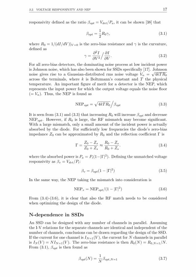
3.2. VOLTAGE RESPONSIVITY AND NEP 17
responsivity defined as the ratio βopt = Vdet/Pa, it can be shown [38] that
βopt =1
2R0γ, (3.1)
where R0 = 1/(dI/dV )|V=0 is the zero-bias resistance and γ is the curvature,defined as
γ =∂2I
∂V 2
/ ∂I
∂V. (3.2)
For all zero-bias detectors, the dominating noise process at low incident poweris Johnson noise, which has also been shown for SSDs specifically [17]. Johnsonnoise gives rise to a Gaussian-distributed rms noise voltage Vn =
√4kTR0
across the terminals, where k is Boltzmann’s constant and T the physicaltemperature. An important figure of merit for a detector is the NEP, whichrepresents the input power for which the output voltage equals the noise floor(= Vn). Thus, the NEP is found as
NEPopt =√4kTR0
/βopt (3.3)
It is seen from (3.1) and (3.3) that increasing R0 will increase βopt and decreaseNEPopt. However, if R0 is large, the RF mismatch may become significant.With a large mismatch, only a small amount of the incident power is actuallyabsorbed by the diode. For sufficiently low frequencies the diode’s zero-biasimpedance Z0 can be approximated by R0 and the reflection coefficient Γ is
Γ =Z0 − Zs
Z0 + Zs≈ R0 − Zs
R0 + Zs. (3.4)
where the absorbed power is Pa = Pi(1−|Γ|2). Defining the unmatched voltageresponsivity as βv = Vdet/Pi:
βv = βopt(1− |Γ|2) (3.5)
In the same way, the NEP taking the mismatch into consideration is
NEPv = NEPopt/(1− |Γ|2) (3.6)
From (3.4)-(3.6), it is clear that also the RF match needs to be consideredwhen optimizing the design of the diode.
N-dependence in SSDs
An SSD can be designed with any number of channels in parallel. Assumingthe I-V relations for the separate channels are identical and independent of thenumber of channels, conclusions can be drawn regarding the design of the SSD.If the current for one channel is IN=1(V ), the current for N channels in parallelis IN (V ) = NIN=1(V ). The zero-bias resistance is then R0(N) = R0,N=1/N .From (3.1), βopt is then found as
βopt(N) =1
Nβopt,N=1 (3.7)

18 CHAPTER 3. INAS SELF-SWITCHING DIODES
since γ is independent of N . In the same way, NEPopt(N) is found from (3.3)as
NEPopt(N) =√N NEPopt,N=1 (3.8)
and the reflection coefficient ΓN as
ΓN =R0,N=1/N − Zs
R0,N=1/N + Zs. (3.9)
Using ΓN and (3.5)-(3.6), expressions for βv(N) and NEPopt(N) can be de-rived. The responsivity and NEP as a function of N , both matched and un-matched is plotted in Fig. 3.3 along with the absorbed power ratio (1− Γ2
N ).The βopt,N=1, NEPopt,N=1, R0,N=1 and Zs used for these plots were chosenarbitrarily. It is seen from βopt and NEPopt that for a matched SSD, N = 1 isclearly favorable. However, N = 1 causes a large R0 and severe mismatch, onlya few percent of incident power is absorbed. In the matched case, βv decreaseswith increased N . However, NEPopt decreases until reaching a minimum at acertain N . The minimum occurs for a lower N than for which R0 = 50 Ω.
This analysis shows that the design for optimal responsivity and NEP dif-fers between the matched and unmatched case. It also shows that a minimumNEPv can be expected for an optimum N .
1 10 100 10001
10
100
N
β v, βop
t (V
/W)
R0=
50 Ω
(a)
1 10 100 100010
100
1000
N
NE
Pv, N
EP
opt (
pW/H
z½)
R0=
50 Ω
(b)
1 10 100 10000.01
0.1
1
N
1−|Γ
|2
R0=
50 Ω
(c)
Figure 3.3: (a) βv (blue) and βopt (red) and (b) NEPv (blue) NEPopt (red)versus number of channels N . (c) Absorbed power ratio versus N . For acertain N , R0 = 50 Ω, indicated by the dashed vertical line.
3.3 Device fabrication
3.3.1 InAs SSDs
The design of the epitaxial structure, particularly the buffer, was crucial forsuccessful fabrication of InAs SSDs. Examples of investigated designs aregiven in Fig. 3.4, together with SEM cross-sections of etched and passivatedSSD trenches. The cross-section was made by fabricating long trenches andthen breaking the substrate perpendicularly to the trenches.
Essentially, the buffer design is a trade-off between chemical stability andisolation. AlSb is known to be prone to oxidation [35] but offers good iso-lation whereas Al80Ga20Sb is more stable but also more conductive [39]. Ina pre-study of InAs SSD fabrication [Paper B], the buffer design illustrated

3.3. DEVICE FABRICATION 19
AlSb
Al80Ga20Sb
AlSb
Substrate
(a)
AlSb
Substrate
(b)
Al80Ga20Sb
AlSb
Substrate
(c)
Figure 3.4: Three buffer designs explored in the development of the InAsSSD process: (a) AlSb/AlGaSb/AlSb buffer [Paper B], (b) pure AlSb and, (c)AlGaSb/AlSb buffer which was used in the final fabrication.
in Fig. 3.4(a) was used. The same buffer design has been successfully im-plemented in InAs/AlSb HEMT fabrication [40]. In this design, a 250 nmAl80Ga20Sb layer was sandwiched between AlSb layers. In the pre-study, InAsSSDs were successfully fabricated by etching through the entire Al80Ga20Sblayer. As shown in Fig. 3.4(a), there was a considerable growth of oxide inthe AlSb. For this reason, the etch is stopped inside the Al80Ga20Sb layer inHEMT fabrication [40]. However, tests showed that if the etch was stoppedin the Al80Ga20Sb layer, the leakage through the residual Al80Ga20Sb wouldmake the resistivity of etched trenches 120 kΩ/sq. Meanwhile, R0 for the fab-ricated SSD was 1.6 MΩ. To maintain a buffer resistance higher than R0, asheet resistance of trenches > 120 MΩ/sq was needed. The Al80Ga20Sb wouldshort-circuit an SSD. Therefore, the Al80Ga20Sb layer was abandoned and thepure AlSb buffer design in Fig. 3.4(b) investigated.
With a pure AlSb buffer, as in Fig. 3.4(b), tests showed that the sheetresistance of trenches would be 75 MΩ, and still cause a significant leakagein comparison to R0 of the SSD. By designing the SSD with many channelsand thus decreasing R0, the leakage current could be made less significant.However, the oxidation could not be overcome. The cross section SEM shownin Fig. 3.4(b) was made only minutes after the trench etch. Despite the sam-ple being passivated with SiNx, the oxidation was clearly visible. To avoidoxidation, an Al80Ga20Sb layer was necessary in the SSD buffer design.
In the final buffer design, shown in Fig. 3.4(c), a 100 nm Al80Ga20Sb-layerwas re-introduced in the top part of the buffer. The trenches were etched justthrough the InAs channel and stopped in the Al80Ga20Sb layer. As seen inFig. 3.4(c), the stability was largely improved. The sheet resistance of trencheswas > 700 MΩ. Hence, the isolation was more than enough for not degradingthe device performance. Since the heterostructure in Fig. 3.4(c) was grown bya different vendor, the reason why the isolation was better than in the pureAlSb buffer was likely different growth conditions. The epitaxial structure is

20 CHAPTER 3. INAS SELF-SWITCHING DIODES
Barrier
Cap layer InAs:Te
Protection Layer InAlAs
Channel
Metamorphic buffer
Substrate 2' S.I GaAs (001)
InAs
50 Å
40 Å
150 Å
1000 Å
GaAs 3000 Å
Al80Ga20Sb 130 Å
Buffer
Metamorphic buffer AlSb
Al80Ga20Sb
10000 Å
Smoothing layer InAlAs 100 Å
Figure 3.5: The developed epitaxial structure used for fabrication of the InAsSSDs. In the top part of the buffer as well as for the barrier, AlSb is exchangedfor Al80Ga20Sb.
Table 3.1: Hall data of InAs and InGaAs SSD wafers. Measured in passivatedregions were the cap layer had been etched away, similar to the active regionsof the SSDs.
SampleRsh
[Ω/sq]ns
[1012 cm−2]µ
[cm2/Vs]InAs 167 1.5 26000
InGaAs 480 0.9 15000
shown in detail in Fig. 3.5. Hall data for this structure is shown in Table. 3.1.Similar carrier concentration and mobility have previously been observed insimilar non-intentionally doped InAs quantum wells [41].
The fabrication of the InAs SSDs was started by the evaporation of Pd/Pt/Au(200/200/600 A) contacts and a subsequent anneal at 275C. After that, metalpads were formed by evaporation of Ti/Au/Ti (200/3000/100 A). Next, thecap layer was recessed in the active area of the device by first removing oxideswith a hydrogen chloride/water solution. The recess etch itself was done withcitric acid/hydrogen peroxide solution. After the recess followed the crucialtrench formation, illustrated in Fig. 3.6. Trenches were patterned in ZEP520Aresist by e-beam lithography. The trench was etched with a Cl:Ar inductively-coupled plasma reactive ion-etch process and stopped in the Al80Ga20Sb bufferjust below the channel. Traditional resist removal techniques such as wet sol-vent processes or oxygen plasma were both inapplicable due to the risk ofinitiating oxidation. Instead, an NF3 plasma was used to remove the resistin situ. Then, approximately 25 nm of silicon nitride (SiNx) was depositedin a room temperature plasma-enhanced chemical vapor deposition process(PECVD). The SiNx was grown in situ, without first exposing the sample toair, in order to temporarily passivate and encapsulate the trenches for the restof the fabrication. The top-view SEM-picture in Fig. 3.7 shows an InAs in thisstate of the fabrication. After the trench formation, mesas were etched in asimilar way as the trenches, but with the etch extended down to the substratefor maximum stability and isolation. The trenches were completely covered byan in situ-grown 180 nm thick SiNx passivation layer deposited using PECVDat room-temperature. A cross-section of etched trenches is shown in 3.7. Theetch was stopped just below the InAs channel. As a final step, openings in the

3.3. DEVICE FABRICATION 21
passivation for metal pads were defined.
3
Trench etch
GaAs substrate
(a)
4
GaAs substrate
NF3 in situ resist removal
(b)
5
GaAs substrate
In situ Si3N4 deposition
(c)
Figure 3.6: InAs SSD trench formation: (a) trench etch, (b) in situ resistremoval, (c) in situ growth of SiNx passivation. The red line represents theInAs channel.
Figure 3.7: Top view SEM image of an InAs SSD after trench fabrication. Theinset shows a SEM cross-section of a finalized SSD channel covered with 180nm SiNx passivation.
3.3.2 InGaAs SSDs
In contrast to InAs SSDs, the fabrication of InGaAs SSDs on an InAlAs bufferwas not complicated by oxidation issues. The epitaxial structure was identicalto the one used for InGaAs slot diodes; see Fig. 2.9. The same structure havebeen used for low-noise InP HEMTs [25]. First, mesas, ohmic contacts andmetals pads were processed in the same way as for slot diodes, described in 2.2.The cap layer was etched away in the active area of the SSDs with a succinicacid/hydrogen peroxide solution. Trenches were pattern by e-beam lithogra-phy in ZEP520A resist. The trenches were etched with a Cl:Ar inductively-coupled plasma reactive ion-etch process just like the InAs SSDs. The resistwas removed in a conventional way with wet solvents and ashing. 25 nm SiNx
passivation was grown in a room temperature plasma-enhanced chemical vapordeposition process. Finally, openings in the passivation were made for metalpads. Hall data from structures processed on the same sample as the InGaAsSSDs is shown in Table. 3.1. Similar values have been reported for the sameepitaxial structure in [27]. As expected, both the carrier concentration andelectron mobility were lower for InGaAs than for InAs.

22 CHAPTER 3. INAS SELF-SWITCHING DIODES
Figure 3.8: Top view and cross-section SEM image of a finalized InGaAs SSD
3.4 Characterization
3.4.1 DC measurements
I-V measurements of an InAs SSD and an InGaAs SSD are presented in Fig. 3.9and Fig. 3.10, respectively. The presented I-V measurements were performedon the SSD which in RF measurements showed the lowest NEPv of all measureddevices in respective technology. For the InAs SSD,N = 43 and for the InGaAsSSD N = 5. Also shown in Fig. 3.9 is the asymmetric current Iasym for thecorresponding devices, defined as Iasym = I(|V |) + I(−|V |). In other words,Iasym represents how much higher the current is in forward bias compared toreverse bias.
The I-V characteristics of the InAs SSD is shown in Fig. 3.9(a). For thisdevice, the current is only slightly higher in forward bias than in reverse bias.As shown in Fig. 3.9(b), Iasym is ≈ 60µA for +0.5 V. The total current is≈ 1 mA. While Iasym of the improved SSD is of the same order of magnitudeas for other non-linear detectors such as Sb-based backward diodes [42], itconstitutes only ≈ 6 % of the total current in the InAs SSD. This large parallelcurrent is due to that the channel does not completely pinch in reverse bias.However, it is this small asymmetry that makes the InAs SSD a detector.
The I-V characteristics of the InGaAs SSDs is shown in Fig. 3.10(a). TheI-V for InGaAs SSD is in many aspects different from the InAs I-V. First, thecurrent in the InGaAs SSD starts to saturate for ≈ 0.1 V. This saturationoccurs also in Id−Vd measurements for Vg = 0 V of InP HEMTs fabricated inthe same heterostructure [29]. Second, the current level is more than a factor100 higher in the InAs SSDs. Per channel, it is 15 times higher. However,asymmetry is stronger in the InGaAs device: Below saturation, Iasym in the

3.4. CHARACTERIZATION 23
−0.5 −0.4 −0.3 −0.2 −0.1 0 0.1 0.2 0.3 0.4 0.5−1.5
−1
−0.5
0
0.5
1
1.5
V (V)
I (m
A)
W=35 nmN=43L=1000 nmWh=100 nmWv=100 nmS=350 nm
(a)
0 0.1 0.2 0.3 0.4 0.50
10
20
30
40
50
60
70
|V| (V)
I asym
[µA
]
(b)
Figure 3.9: (a) I-V characterization of an InAs SSD and (b) the asymmetriccurrent Iasym.
−0.5 −0.4 −0.3 −0.2 −0.1 0 0.1 0.2 0.3 0.4 0.5−20
−10
0
10
20
V (V)
I (µA
)
W=50 nmN=5L=1000 nmWh=50 nmWv=50 nmS=2000 nm
(a)
0 0.1 0.2 0.3 0.4 0.50
2
4
6
8
10
|V| (V)
I asym
[µA
]
(b)
Figure 3.10: (a) I-V characterization of an InGaAs SSD and (b) the asymmet-ric current Iasym.
InGaAs SSD comprises ≈ 15 % of the total forward current.Responsivity and NEP can be derived from measured I-V according to
(3.1)-(3.3). The values in Table 3.2 have been derived from the I-V measure-ments presented in Fig. 3.9 and Fig. 3.10. In comparison to the InGaAs SSD,the InAs SSD has higher NEPopt and much lower βopt. However, the signifi-cantly lower R0 makes the power transfer from a 50 Ω system easier with theInAs SSD than for the InGaAs SSD.
DC-measurements of R0 and γ at zero bias as a function of W is shown inFig. 3.11. For InGaAs devices, R0 is many kΩ for small W , making matchingdifficult. Smaller W leads to higher γ in both InAs SSDs and InGaAs SSDs,reaching maximally 0.2 V−1 and 2.5 V−1, respectively. For comparison, zero-bias Schottky diodes and Sb-heterostructure diodes have γ of 26 and 47 V−1
respectively, leading to the high responsivities observed with those diodes [7,43].

24 CHAPTER 3. INAS SELF-SWITCHING DIODES
Table 3.2: Detector characteristics of InAs and InGaAs SSDs derived fromI-V measurements. Derived from the I-V characteristics shown in Fig. 3.9 andFig. 3.10
R0
(Ω)βopt
(V/W)NEPopt
(pW/Hz1/2)βv
(V/W)NEPv
(pW/Hz1/2)InAs SSD 350 18 200 11 210InGaAs SSD 1800 14000 1.2 150 115
0 20 40 60 80 100 1200
50
100
150
200
250
300
350
400
R0 (
Ω)
W (nm)
0
0.1
0.2
0.3
0.4
0.5
γ (1
/V)
InAs
(a)
0 20 40 60 80 100 1200
50
100
150
200
250
300
R0 (
kΩ)
W (nm)
0
0.5
1
1.5
2
2.5
3
γ (1
/V)
InGaAs
(b)
Figure 3.11: R0 (crosses) and zero-bias γ (circles) versus W in (a) InAs SSDsand (b) InGaAs SSDs. Other design parameters according to Fig. 3.9 andFig. 3.10.
3.4.2 Cryogenic DC measurements
I-V measurements were carried out on an InAs SSD at 6 K and compared toroom temperature measurement [Paper D]. The InAs SSDs were fabricatedas described in section 3.3.1, with the difference that the cap layer was notremoved in this particular diode.
Hall measurements were performed on a sample processed like the SSD,but with the cap layer etched away. By etching away the cap, the transportproperties in the 2DEG only were investigated. Table 3.3 shows how thesheet resistance Rsh is virtually unaffected upon cooling from 300 K to 77 Kwhereas the sheet carrier concentration ns is halved and mobility µ doubled.The transport properties are not expected to differ significantly between 6 Kand 77 K [41].
In Fig. 3.12(a), the diode current I versus applied voltage V is plotted at300 K and 6 K. The resistance for small V increases upon cooling, from 2.8 kΩto 6.9 kΩ. From the Hall measurements on the 2DEG showed in Table 3.3,the resistance is expected to stay about the same. A possible reason for thediscrepancy is the geometry. At 6 K, charges on the trench sidewalls maydeplete the channel further, thus narrowing the effective channel width. Forlarger V , current increases rapidly. This may be due to impact ionization.
βopt versus V was calculated according to (3.1)-(3.3). At 300 K and 6 K,βopt were 490 and 4400 V/W, respectively. Corresponding NEPopt was 14and 0.34 pW/Hz1/2. Thus, the performance of the InAs SSD can be expectedto improve upon cooling. This has been verified with RF measurements inInGaAs SSDs [11], but not so far in InAs SSDs.

3.4. CHARACTERIZATION 25
Table 3.3: Hall measurements for InAs SSDs at 300 K and 77 K. The Hallsample was prepared like the InAs SSDs, except for the cap layer which wasetched away to reveal the properties of the 2DEG.
Rsh (Ω/sq) ns (cm−2) µ (cm2/Vs)300 K 181 1.3× 10¹² 2600077 K 175 6.3× 10¹¹ 57000
−0.5 −0.4 −0.3 −0.2 −0.1 0 0.1 0.2 0.3 0.4 0.5−200
−150
−100
−50
0
50
100
150
200
I (µA
)
V (V)
300 K6 K
(a)
−100 −50 0 50 1000
2 500
5 000
7 500
10 000
V (mV)
β opt (
V/W
)
300 K6 K
490 V/W
4400 V/W
(b)
Figure 3.12: (a) I-V measurements and (b) derived βopt for an InAs SSD at300 K and 6 K.
3.4.3 On-wafer RF measurements
Agilent E8361A, 2-50 GHz
Rhode & Schwarz ZVA-24,
140-200 GHz, 220-315 GHz
Ch A Ch B
Probe +
bias tee
+_
PiLP0
Vdet
SSD on
wafer
Figure 3.13: Schematic view of the setup for on-wafer characterization of InAsand InGaAs SSDs.
On-wafer measurements were performed using a vector network analyzeras the signal source. The setup is shown in 3.13. Different equipment wasused for each of the three different bands (2-50, 140-220 and 240-315 GHz), allfollowing the same principle: The power from the source was measured with acalorimetric power meter for each frequency setting. By subtracting the lossof the RF probes, the available power at the probe tip was found. The powerincident to the device was 1.7−8.5 µW, delivered by a 50 Ω source. ResultingDC detection voltage was measured through a bias-tee with a high-resistanceload. The unmatched responsivity βv was found as the ratio βv = Vdet/Pi.
The influence of design parameters W on responsivity and NEP was stud-ied at 50 GHz. Typical designs for InAs and InGaAs SSDs are shown in

26 CHAPTER 3. INAS SELF-SWITCHING DIODES
Table 3.4: Typical SSD designs fabricated in InAs SSDs and InGaAs.
MaterialW
(nm)N L
(nm)Wh
(nm)Wv
(nm)Wmesa
(µm)InAs 45 43 1100 100 100 30InGaAs 45 5 1100 50 50 15
0 50 100 150 200 250 300 350
5
10
15
20
25
Frequency [GHz]
β v (V
/W) W=35 nm
W=45 nm
W=120 nm
InAs
(a)
0 50 100 150 200 250 300 350
100
200
300
400
500
Frequency [GHz]
βv (
V/W
)
W=35 nm
W=50 nm
W=90 nm
InGaAs
(b)
Figure 3.14: βv derived from on-wafer RF measurements for (a) InAs SSDsand (b) InGaAs SSDs.
Table 3.4. Based on these designs, W -dependence was tested by measuring ondifferent SSDs, varying only W . For InAs SSDs, also N - and L- dependencewas investigated.
Fig. 3.14(a) shows βv as a function of frequency for InAs SSDs, with threedifferent W . The ripple in the data is attributed to the fact that when P0 wasmeasured with the power meter, the source saw a different load than when theSSDs were measured. Notably, no strong roll-off is observed in the measuredband up to 315 GHz, in particular for W = 45 nm and W = 120 nm. Thehighest βv is achieved for W = 35 nm, for which βv > 10 V/W in the measuredband. For larger W , βv is lower, but shows very similar frequency dependence.Fig. 3.14(b) shows the corresponding data for InGaAs SSDs. Generally, βv inthe InGaAs SSDs is higher than in the InAs SSDs. The difference in βv
between the two materials is consistent with the observation in section 3.4.1that InGaAs SSDs have a more nonlinear I-V relation than InAs SSDs.

3.4. CHARACTERIZATION 27
0 20 40 60 80 100 1200
5
10
15
20
W (nm)
β v (V
/W)
InAs
(a)
0 20 40 60 80 100 1200
100
200
300
400
W (nm)
β v (V
/W)
InGaAs
(b)
Figure 3.15: βv at 50 GHz. For (a) InAs SSDs, (b) InGaAs SSDs.
Design dependence
W -dependence
The channel width W is an important design parameter in the SSD. A detailedstudy of how βv depends on W is shown in Fig. 3.15 for InAs and InGaAsSSDs. The measurement was performed at 50 GHz with an incident powerof 3.2 µW. Clearly, βv was higher for small W . The exact dependence onW is more easily understood by studying βopt, which is done in Fig. 3.16.For InAs SSDs, βopt was found as βopt = βv/(1 − |Γ|2), where Γ was themeasured reflection coefficient. For InGaAs SSDs, R0 >> 1 kΩ, thus Γ wasclose to 1 and hard to measure. Instead Γ for InGaAs SSDs was found fromDC-measurements according to (3.4). For both materials the highest βopt, 34V/W and 270 kV/W for InAs and InGaAs respectively, was achieved for thesmallest W investigated.
Shown in 3.16(a) is also βopt as derived from I-V characterizations. Thesederivations were done according to (3.1)-(3.3) by fitting a 5th-order polynomialto measured I-V characteristics for V ∈ [0.2, 0.2] V. The βopt derived in thisway matched the measured βopt closely, both in a relative and absolute sense.This opens for further understanding of the effect of scaling W by studyingdifferent contributions to βopt, based on (3.1). For InAs SSDs, from W = 120to 35 nm, βopt increased from 6.5 to 34 V/W, corresponding to a 420% increase.In Fig. 3.11, DC analysis showed that the increase in R0 was 180 % (from 126 to350 Ω) and in γ, 100 % (from 0.1 to 0.2 V−1). The increase in γ is importantsince it shows that the increase in βopt was not merely due to an increasedR0, but also an increased non-linearity of the current in each channel. Asexplained in section 3.2, an increased R0 increases βopt, but will also increasethe mismatch. For InGaAs SSDs, from W = 90 to 20 nm, βopt increased from3.2 to 270 kV/W, and γ 260 %.
NEPv and NEPopt versus W were calculated according to (3.3) and (3.6)and are plotted in Fig. 3.17. For InAs SSDs, the lowest NEPv and NEPopt
were 150 and 70 pW/Hz1/2, respectively. For InGaAs SSDs, correspondingvalues were 60 and 0.3 pW/Hz1/2. NEPv=64 pW/Hz1/2 has been reported forInGaAs SSDs elsewhere, for a design with N=2000 [17]. Here, similar NEPv
is achieved with N=5.

28 CHAPTER 3. INAS SELF-SWITCHING DIODES
0 20 40 60 80 100 1200
10
20
30
40
W (nm)
β opt (
V/W
)InAs
(a)
0 20 40 60 80 100 1200
50
100
150
200
250
300
W (nm)
β opt (
kV/W
)
InGaAs
(b)
Figure 3.16: βopt versus W , as measured (crosses) and calculated from I-Vmeasurements (circles). For (a) InAs SSDs, (b) and InGaAs SSDs.
In InAs SSDs, the lowest NEPv and NEPopt are achieved for the lowestW . Scaling of W may thus further improve the device. In this study, both theminimum NEPv and NEPopt were considerably lower in InGaAs SSDs than inInAs SSDs. For InGaAs SSDs, W = 50 nm optimal in terms of NEPv. Forsmaller W , the large increase of R0 caused the noise to increase.
0 20 40 60 80 100 1200
100
200
300
400
W (nm)
NE
Pv, N
EP
opt (
pW/H
z½)
InAs
(a)
0 20 40 60 80 100 1200
50
100
150
200
NE
Pv (
pW/H
z½)
W (nm)
0
1
2
3
4
5
NE
Pop
t (pW
/Hz½
)
InGaAs
(b)
Figure 3.17: NEPv (red crosses) and NEPopt (circles) versus W measured at
N-dependence
In InAs SSDs, also the N dependence was studied, with results shown inFig. 3.18. From the N=43 device, R0,N=1 and βopt,N=1 was extracted. Using(3.7)-(3.9), βv(N) and βopt(N), as well as NEPv(N) and NEPopt(N) could beplotted in Fig. 3.18 and compared to measurements. The agreement is good,with some discrepancy for small N . Is is shown that as NEPopt increased forhigher N , NEPv decreased. This is explained by the decreased R0 for large N ,resulting in reduced mismatch. Fig. 3.18(b) further suggests that increasingN beyond 40 has little effect on NEPv even if the expected minimum occursfor N = 70.

3.4. CHARACTERIZATION 29
0
5
10
15
20
β v (V
/W)
0 20 40 60 80 1000
50
100
150
200
β opt (
V/W
)
N
InAs
(a)
0 20 40 60 80 1000
100
200
300
400
N
NE
Pv, N
EP
opt (
pW/H
z½) InAs
(b)
Figure 3.18: βopt and NEPopt (circles), and βv and NEPv (crosses) versus N ,measured at 50 GHz. The theoretical relation (black lines) was derived fromthe value of βopt,N=43 and R0,N=43.
0 500 1000 1500 20000
5
10
15
20
25
30
L (nm)
β v, βop
t (V
/W)
InAs
(a)
0 500 1000 1500 20000
100
200
300
400
500
L (nm)
NE
Pv, N
EP
opt (
pW/H
z½) InAs
(b)
Figure 3.19: βopt and NEPopt (circles), and βv and NEPv (crosses) versus L.Measured at 50 GHz.
L-dependence
The last design parameter investigated was the L-dependance, shown in Fig. 3.19.Increased L increases βopt and decreases NEPopt. Also βv and NEPv are im-proved, but to a lesser extent due to increased R0 and thus increased mismatch.
3.4.4 Free-space RF measurements
To investigate if the SSDs could function as a detector at 600 GHz, a free-spacesetup was used, shown in Fig. 3.20. A measurement at 200 GHz was conductedin a similar way, for comparison with the on-wafer results. A detector was builtfrom an InAs SSD contained within a circularly polarized spiral substrateantenna [44], for which the simulated impedance was plotted in Fig. 2.12.The SSD design was N = 11, W = 65 nm, otherwise according to Table 3.4.From I-V characterization, βopt = 53 V/W is expected. A silicon lens wasplaced firmly against the backside of the substrate with the SSDs. The outputvoltage was measured with a lock-in amplifier, thus presenting a high DC-load.

30 CHAPTER 3. INAS SELF-SWITCHING DIODES
Lock-in
amp.
Silicon lens
Substrate
antenna with SSD
Chopper
Horn
antenna
500 µm
x6+
amp
x2 @200 GHz
x6 @600 GHz
Figure 3.20: The setup used for free-space measurements at 200 and 600 GHz.
On the transmitter side, the vertically polarized beam was radiated througha conical horn antenna. By replacing the receiver with an Erickson PM4power meter with a horn antenna, the incident power was measured. At 200GHz and 600 GHz the power in pulses was 1.15 mW and 7 µW, respectively.The responsivity of the system at 200 GHz and 600 GHz was 2.1 V/W and0.70 V/W, respectively. Compensating for polarization mismatch (50%) andthe mismatch between R0 and the antenna radiation resistance (≈ 50 %), βopt
is calculated to 8.4 V/W and 2.8 V/W at 200 and 600 GHz, respectively.In the on-wafer RF measurements, measured βopt matches the one calcu-
lated from I-V measurements, see Fig. 3.16. The discrepancy between the βopt
measured in the free-space setup at 200 GHz and the βopt calculated from I-Vmeasurements may be due to other losses than what was compensated for.For example, reactive contributions was not considered when calculating theantenna mismatch, nor the fact that not all incident power is coupled into theantenna. However, it was confirmed that InAs SSDs can function as detec-tors at 600 GHz, with a responsivity of the same order of magnitude as for200 GHz. This find motivates further investigation of InAs SSD detection at600 GHz and higher frequencies.
3.4.5 InAs SSD imaging
With the same SSD used for free-space detection (N = 11, W = 65 nm), theimaging setup in Fig. 3.21 was used to image an RFID card. The imagingwas performed at 200 GHz with an output power of 1.15 mW. The beamwas focused on the RFID card shown in Fig. 3.22. The card was movedin a grid pattern and the output voltage Vdet in the SSD was recorded forevery point. Plotting the signal strength versus position resulted in the imageshown in Fig. 3.22. The plastics of the card is transparent to the radiationand thus imaged bright, while the metal antenna and microchip are reflectiveand imaged dark.

3.4. CHARACTERIZATION 31
Lock-in
amp.
Silicon lens
Substrate
antenna with SSD
ChopperHorn
antenna
xy
RFID card
x-y board
500 µm
x6+
ampx2
Figure 3.21: Setup used for imaging at 200 GHz with an InAs SSD. Sphericalmirrors were used to focus the beam.
(a) (b)
Figure 3.22: (a) An RFID card and (b) its image when irradiated by 200 GHzwaves and detected by the InAs SSD.
3.4.6 Characterization summary
DC-characterization if InAs SSDs were performed in which a relatively smallnonlinearity was observed. Upon cooling to 6 K, this nonlinearity increasedcompared to at 300 K, increasing βopt tenfold.
InAs and InGaAs SSDs were characterized as room-temperature detectorson-wafer in the range 2-315 GHz, in which no strong roll-off of responsivitywas observed. A comparison of different designs were made at 50 GHz. It wasshown that for the range of designs tested, NEPv benefits from larger L andsmaller W . For InAs SSDs, larger N will not reduce NEPv significantly. ForInGaAs, larger N may lower NEPv.
For InAs SSDs, measured at 50 GHz, the highest βv and lowest NEPv
observed were 17 V/W and 150 pW/Hz1/2, respectively. For the same device,the R0 was 350 Ω, making the mismatch fairly low. With a conjugate match,

32 CHAPTER 3. INAS SELF-SWITCHING DIODES
34 V/W and 70 pW/Hz1/2 is expected.InGaAs SSDs were studied in parallel. Compared to InAs SSDs, InGaAs
SSDs are more resistive and suffer from a larger mismatch, but also havea larger γ. The lowest NEPv observed at 50 GHz when measured a 50 Ωsource was 60 pW/Hz1/2, for a device with N =. Corresponding βv was280 V/W. Similar NEPv has been observed in InGaAs previously, then withN = 2000 [17].
A free-space detector was designed and fabricated from an InAs SSDs.The responsivity of the detector was 2.1 V/W and 0.70 V/W at 200 GHzand 600 GHz, respectively. Several losses not compensated for may explainwhy the responsivity from free-space characterization was lower than than incorresponding DC and on-wafer RF measurements. Furthermore, the free-space experiment showed that the InAs SSD operated up to 600 GHz.
Finally, an imaging experiment was performed. An RFID card was imagedat 200 GHz using InAs SSDs.

Chapter 4
Conclusions and futurework
This thesis describes the fabrication and characterization of InGaAs slot diodesfor THz emission, and InAs SSDs for THz detection, both at room-temperatureconditions. Also, the more established InGaAs SSDs were studied thus allow-ing to benchmark with the InAs SSDs.
InGaAs slot diodes were designed in an epitaxial InGaAs heterostructurewith a lateral design according to MC simulation results [21]. I-V measure-ments of fabricated slot diodes at 300 K were well reproduced by MC simula-tions which predicted emission around 1 THz. Trap-related phenomena wereobserved in I-V measurements on slot diodes at 6 K. Despite the fact that MCsimulations predicted an output power of 50 µW at 0.8 THz or higher, no THzemission was detected from slot diodes in measurements up to 1 THz with anoise floor of 10 nW.
In future investigations of THz emission in InGaAs slot diodes, emissionat higher frequencies should be investigated. Since electron mobility increasesupon cooling, cryogenic emission experiments may be rewarding.
InAs self-switching diodes have been fabricated and characterized as de-tectors for the first time. The responsivity of InAs SSDs was measured on-wafer in the range 2-315 GHz, in which no roll-off of responsivity was ob-served. The highest responsivity and lowest NEP observed were 17 V/W and150 pW/Hz1/2, respectively, measured at 50 GHz with a 50 Ω source andno matching network. With a conjugately matched source a responsivity of34 V/W and NEP of 65 pW/Hz1/2 are expected, based on S-parameters andresponsivity as measured with a 50 Ω source. In a free-space detection ex-periment, an InAs SSD detector with a substrate antenna was demonstratedat 600 GHz. For InGaAs SSDs, the lowest noise equivalent power when mea-sured at 50 GHz with a 50 Ω source was 60 pW/Hz1/2 and the responsivity280 V/W. Up to at least 315 GHz, the maximum frequency in the on-wafermeasurements, the InGaAs SSDs outperform the InAs SSDs in terms of re-sponsivity and NEP. However, in the THz range, InAs SSDs may challengeboth InGaAs SSDs and other detector technologies.
An experimental study of how the design influences the SSD detectionperformance was reported for the first time. Also, it was successfully shown
33

34 CHAPTER 4. CONCLUSIONS AND FUTURE WORK
that DC measurements can be used to predict the responsivity of SSDs.This thesis has demonstrated the feasibility of InAs SSDs for THz detec-
tion. Compared to other detectors, there is still much improvement to be donein order to enhance responsivity and reduce NEP. However, the potential fordetection above 1 THz is there, and with improved technology, optimized de-sign (including antenna) and adequate measurements, InAs SSD technologymay become a viable detector for THz applications. Since SSDs can be fab-ricated in the same heterostructure as HEMTs, MMIC integration may beexplored.

Acknowledgement
I want to thank the people that made this work possible.Prof. Jan Grahn for hiring me, supervising me and encouraging me in my
work. It was a long walk until the break-through for InAs SSDs.My examiner Prof. Jan Stake for sharing general knowledge on THz de-
vices.Dr. Per-Ake Nilsson for showing me how to work in the lab and having
fruitful discussions on fabrication and physics.My friend Dr. Giuseppe Moschetti for helping me getting started with the
tricky AlSb-materials in the lab. Without his help, this work would have takenmuch longer time to complete.
For growth of InAs/AlSb material for the first InAs SSD, Dr. Huan Zhao.I also want to thank Dr. Ludovic Desplanque and Prof. Xavier Wallart atUniversity of Lille, France for growing for the collaboration on growth.
Niklas Wadefalk, for showing me various software and equipment in themeasurement lab. I want to thank Dr. Serguei Cherednichenko for explainingfree-space measurements to me.
I want to thank the MC2 clean room staff for maintaining a collaborativeatmosphere in the clean room.
The work described in this licentiate thesis was to a large extent performedthrough an international collaboration. I want to thank all the colleagues inthe project. At University of Salamanca in Spain I would like to thank Dr.Susana Perez, for discussions and Mc simulations on slot diodes, Dr. IgnacioIniguez-de-la-Torre for discussions on SSDs and sight-seeing in Salamanca. Iwant to thank Dr. Thomas Gonzalez, and for coordinating the project; Prof.Javier Mateos. At the University of Lille in France, I would like to thank Prof.Christophe Gaquiere, Dr. Guillaume Ducournau and Paul Sangare for theirmeasurement efforts and great hospitality during my visit. At the Universityof Manchester in UK, I want to thank Prof. Aimin Song, Linqing Zhang andYasaman Alimi for bolometer measurements on slot diodes.
I want to thank David Gustafsson, Olle Axelsson, Christer Andersson ,Mustafa Ozen, Klas Eriksson, Dr. Helena Rodilla, Joel Schleeh and everyoneelse at MEL and TML for making it fun to come to work.
Most of all, I want to thank Rebecca.
This work has been supported by the European Commission through theROOTHz Project ICT-2009-243845.
35


Bibliography
[1] P. H. Siegel, “THz Instruments for Space,” IEEE Transactions onAntennas and Propagation, vol. 55, no. 11, pp. 2957–2965, Nov. 2007.
[2] R. Appleby and R. N. Anderton, “Millimeter-Wave and Submillimeter-Wave Imaging for Security and Surveillance,” Proceedings of the IEEE,vol. 95, no. 8, pp. 1683–1690, Aug. 2007.
[3] J. Federici and L. Moeller, “Review of terahertz and subterahertzwireless communications,” Journal of Applied Physics, vol. 107, no. 11,p. 111101, 2010.
[4] S. Perez, T. Gonzalez, D. Pardo, and J. Mateos, “Terahertz Gunn-likeoscillations in InGaAs/InAlAs planar diodes,” Journal of AppliedPhysics, vol. 103, no. 9, p. 094516, 2008.
[5] J. L. Hesler and T. W. Crowe, “Responsivity and noise measurements ofzero-bias Schottky diode detectors,” in 18th Intl. Symp. Space TerahertzTech., Pasadena, CA, 2007.
[6] S. Sze and K. K. Ng, Physics of Semiconductor Devices. Hoboken, NJ,USA: John Wiley & Sons, Inc., Oct. 2006.
[7] D. Schoenherr, C. Bleasdale, T. Goebel, C. Sydlo, H. L. Hartnagel,R. Lewis, and P. Meissner, “Extremely broadband characterization of aSchottky diode based THz detector,” in 35th International Conferenceon Infrared, Millimeter, and Terahertz Waves, pp. 1–2, Sep. 2010.
[8] N. Su, Z. Zhang, R. Rajavel, P. Deelman, J. Schulman, andP. Fay, “Scaling of High-Performance InAs/AlSb/GaSb HeterostructureDetectors for Millimeter-Wave and Submillimeter-Wave Sensing andImaging,” in 2008 Device Research Conference, pp. 123–124, Jun. 2008.
[9] N. Su, Z. Zhang, J. N. Schulman, and P. Fay, “Temperature Dependenceof High Frequency and Noise Performance of Sb-HeterostructureMillimeter-Wave Detectors,” IEEE Electron Device Letters, vol. 28, no. 5,pp. 336–339, May 2007.
[10] A. M. Song, M. Missous, P. Omling, A. R. Peaker, L. Samuelson,and W. Seifert, “Unidirectional electron flow in a nanometer-scalesemiconductor channel: A self-switching device,” Applied PhysicsLetters, vol. 83, no. 9, p. 1881, Sep. 2003.
37

38 BIBLIOGRAPHY
[11] C. Balocco, M. Halsall, N. Q. Vinh, and A. M. Song, “THz operation ofasymmetric-nanochannel devices.” Journal of physics. Condensed matter:an Institute of Physics journal, vol. 20, no. 38, p. 384203, Sep. 2008.
[12] C. Balocco, S. R. Kasjoo, X. F. Lu, L. Q. Zhang, Y. Alimi, S. Winnerl,and A. M. Song, “Room-temperature operation of a unipolar nanodiodeat terahertz frequencies,” Applied Physics Letters, vol. 98, no. 22, p.223501, 2011.
[13] P. Sangare, G. Ducournau, B. Grimbert, V. Brandli, M. Faucher,C. Gaquieere, A. Iniguez-de-la Torre, I. Iniguez-de-la Torre, J. F.Millithaler, J. Mateos, and T. Gonzalez, “Experimental demonstrationof direct terahertz detection at room-temperature in AlGaN/GaNasymmetric nanochannels,” Journal of Applied Physics, vol. 113, no. 3,p. 034305, Jan. 2013.
[14] M. Y. Irshaid, C. Balocco, Y. Luo, P. Bao, C. Brox-Nilsen, andA. M. Song, “Zinc-oxide-based planar nanodiodes operating at 50 MHz,”Applied Physics Letters, vol. 99, no. 9, p. 092101, Aug. 2011.
[15] J. Kettle, R. Perks, and R. Hoyle, “Fabrication of highly transparentself-switching diodes using single layer indium tin oxide,” ElectronicsLetters, vol. 45, no. 1, p. 79, 2009.
[16] L. Majewski, C. Balocco, R. King, S. Whitelegg, and A. Song, “Fastpolymer nanorectifiers for inductively coupled RFID tags,” MaterialsScience and Engineering: B, vol. 147, no. 2-3, pp. 289–292, Feb. 2008.
[17] C. Balocco, S. R. Kasjoo, L. Q. Zhang, Y. Alimi, and A. M. Song,“Low-frequency noise of unipolar nanorectifiers,” Applied Physics Letters,vol. 99, no. 11, p. 113511, Sep. 2011.
[18] I. Iniguez-de-la Torre, H. Rodilla, J. Mateos, D. Pardo, A. M. Song, andT. Gonzalez, “Terahertz tunable detection in self-switching diodes basedon high mobility semiconductors: InGaAs, InAs and InSb,” in Journalof Physics: Conference Series, vol. 193, p. 012082, Nov. 2009.
[19] S. Perez, J. Mateos, D. Pardo, and T. Gonzalez, “Excitationof millimeter-wave oscillations in InAlAs/InGaAs heterostructures,”Physica Status Solidi, vol. 5, no. 1, pp. 146–149, Jan. 2008.
[20] S. Perez, J. Mateos, and T. Gonzalez, “Submillimeter-Wave Oscillationsin Recessed InGaAs/InAlAs Heterostructures: Origin and Tunability,”Acta Physica Polonica A, vol. 119, no. 2, pp. 111–113, 2011.
[21] S. Perez, J. Mateos, D. Pardo, and T. Gonzalez, “On the geometricaltunabililty of THz Gunn-like oscillations in InGaAs/InAlAs slot diodes,”in Journal of Physics: Conference Series, vol. 193, p. 012090, Nov. 2009.
[22] J. L. Thobel, L. Baudry, A. Cappy, P. Bourel, and R. Fauquembergue,“Electron transport properties of strained In(x)Ga(1 x)As,” AppliedPhysics Letters, vol. 56, no. 4, p. 346, 1990.

BIBLIOGRAPHY 39
[23] S. Perez, Departamento de Fısica Aplicada, Facultad de Ciencias, Uni-versidad de Salamanca, Salamanca, Spain. Personal communication.
[24] M. Malmkvist, S. Wang, and J. Grahn, “Epitaxial Optimizationof 130-nm Gate-Length InGaAs/InAlAs/InP HEMTs for Low-NoiseApplications,” IEEE Transactions on Electron Devices, vol. 56, no. 1,pp. 126–131, Jan. 2009.
[25] J. Schleeh, G. Alestig, J. Halonen, A. Malmros, B. Nilsson, P. A. Nilsson,J. P. Starski, N. Wadefalk, H. Zirath, and J. Grahn, “Ultralow-PowerCryogenic InP HEMT With Minimum Noise Temperature of 1 K at 6GHz,” IEEE Electron Device Letters, vol. 33, no. 5, pp. 664–666, May2012.
[26] H. Fourre, “Selective wet etching of lattice-matched InGaAs/InAlAson InP and metamorphic InGaAs/InAlAs on GaAs using succinicacid/hydrogen peroxide solution,” Journal of Vacuum Science &Technology B: Microelectronics and Nanometer Structures, vol. 14, no. 5,p. 3400, Sep. 1996.
[27] H. Rodilla, J. Schleeh, P.-A. Nilsson, N. Wadefalk, J. Mateos, andJ. Grahn, “Cryogenic Performance of Low-Noise InP HEMTs: A MonteCarlo Study,” IEEE Transactions on Electron Devices.
[28] J. Mateos, “ROOTHz 2nd Year Progress Report,” 2011.
[29] J. Schleeh, J. Halonen, B. Nilsson, P. A. Nilsson, L. J. Zeng, P. Ram-vall, N. Wadefalk, H. Zirath, E. Olsson, and J. Grahn, “Passivation ofInGaAs/InAlAs/InP HEMTs using Al2O3 atomic layer deposition,” inIPRM 2011 23rd International Conference on Indium Phosphide and Re-lated Materials, pp. 1–4, 2011.
[30] P. Sangare, G. Ducourneau, and C. Gaguiere, Institute of Electronics, Mi-croelectronics and Nanotechnology, University of Lille, Villeneuve d’Ascq,France. Personal communication.
[31] A. Song, L. Zhang, and Y. Alimi, School of Electrical and ElectronicEngineering, The University of Manchester, Manchester, UK. Personalcommunication.
[32] C. Liu, “Progress in Antimonide Based III-V Compound Semiconductorsand Devices,” Engineering, vol. 02, no. 08, pp. 617–624, 2010.
[33] L. Q. Zhang, Y. Alimi, C. Balocco, H. Zhao, A. Westlund, G. Moschetti,P.-A. Nilsson, J. Grahn, and A. M. Song, “Fabrication of novel unipolarnanodiodes in InAs/AlSb for microwave detection,” in 2011 InternationalConference on Infrared, Millimeter, and Terahertz Waves, pp. 1–2, Oct.2011.
[34] A. Westlund, G. Moschetti, H. Zhao, P.-A. Nilsson, and J. Grahn,“Fabrication and DC characterization of InAs/AlSb self-switchingdiodes,” in 2012 International Conference on Indium Phosphide andRelated Materials, pp. 65–68, Aug. 2012.

40 BIBLIOGRAPHY
[35] A. Olivier, T. Gehin, L. Desplanque, X. Wallart, Y. Roelens,G. Dambrine, A. Cappy, S. Bollaert, E. Lefebvre, M. Malmkvist, andJ. Grahn, “AlSb/InAs HEMTs on InP substrate using wet and dryetching for mesa isolation,” in 2008 20th International Conference onIndium Phosphide and Related Materials, pp. 1–3, May 2008.
[36] M. A berg, J. Saijets, A. Song, and M. Prunnila, “Simulation andModeling of Self-switching Devices,” Physica Scripta, vol. T114, pp.123–126, Jan. 2004.
[37] I. Iniguez-de-la Torre, J. Mateos, D. Pardo, A. M. Song, and T. Gonzalez,“Enhanced Terahertz detection in self-switching diodes,” InternationalJournal of Numerical Modelling: Electronic Networks, Devices andFields, vol. 23, no. 4-5, pp. 301–314, Nov. 2009.
[38] A. Cowley and H. Sorensen, “Quantitative Comparison of Solid-StateMicrowave Detectors,” IEEE Transactions on Microwave Theory andTechniques, vol. 14, no. 12, pp. 588–602, Dec. 1966.
[39] P. Nam, R. Tsai, M. Lange, W. Deal, J. Lee, C. Namba, P. Liu, R. Grund-bacher, J. Wang, M. Barsky, and Others, “Shallow mesa isolation ofAlSb/InAs HEMT with AlGaSb buffer layer using inductively coupledplasma etching,” in Proc. Int. Conf. Compound Semicond. Manuf. Tech-nol.(GaAs Mantech), 2005.
[40] G. Moschetti, N. Wadefalk, P.-A. k. Nilsson, Y. Roelens, A. Noudeviwa,L. Desplanque, X. Wallart, F. Danneville, G. Dambrine, S. Bollaert, andJ. Grahn, “InAs/AlSb HEMTs for cryogenic LNAs at ultra-low powerdissipation,” Solid-State Electronics, vol. 64, no. 1, pp. 47–53, Oct. 2011.
[41] G. Tuttle, H. Kroemer, and J. H. English, “Electron concentrationsand mobilities in AlSb/InAs/AlSb quantum wells,” Journal of AppliedPhysics, vol. 65, no. 12, p. 5239, Jun. 1989.
[42] N. Su, R. Rajavel, P. Deelman, J. Schulman, and P. Fay, “Sb-Heterostructure Millimeter-Wave Detectors With Reduced Capacitanceand Noise Equivalent Power,” IEEE Electron Device Letters, vol. 29,no. 6, pp. 536–539, Jun. 2008.
[43] R. Rajavel, P. Deelman, and P. Fay, “Sub-Micron Area Heterojunction
Backward Diode Millimeter-Wave Detectors With 0.18 pW/Hz(1/2)Noise Equivalent Power,” IEEE Microwave and Wireless ComponentsLetters, vol. 21, no. 5, pp. 267–269, May 2011.
[44] A. D. Semenov, H. Richter, H.-W. Hubers, B. Gunther, A. Smirnov,K. S. Il’in, M. Siegel, and J. P. Karamarkovic, “Terahertz Performanceof Integrated Lens Antennas With a Hot-Electron Bolometer,” IEEETransactions on Microwave Theory and Techniques, vol. 55, no. 2, pp.239–247, Feb. 2007.

Paper A
Terahertz Detection in InAs/Al0.8Ga0.2Sb Self-SwitchingDiodes at Room Temperature and Zero Bias
A. Westlund, P. Sangare, G. Ducournau, P-A. Nilsson, C. Gaquiere,L. Desplanque, X. Wallart, J. Grahn
Manuscript, May 2013.


Paper B
Fabrication and DC characterization of InAs/AlSb Self-Switching Diodes
A. Westlund, G. Moschetti, H. Zhao, P-A. Nilsson, J. Grahn
IEEE 24th International Conference on Indium Phosphide & RelatedMaterials, IPRM, pp. 65-68, Aug 2012


Paper C
Fabrication and Characterization of InGaAs/InAlAs Slotdiodes
A. Westlund, P-A. Nilsson, J. Grahn
37th Workshop on Compound Semiconductor Devices and IntegratedCircuits held in Europe, WOCSDICE, May 2011


Paper D
Cryogenic DC Characterization of InAs/Al0.8Ga0.2Sb Self-Switching Diodes
A. Westlund, G. Moschetti, P-A. Nilsson, J. Grahn, L. Desplanque,X. Wallart
IEEE 25th International Conference on Indium Phosphide & RelatedMaterials, IPRM, May 2013