novel photocatalytic tio2-based porous membranes prepared
TRANSCRIPT

HAL Id: tel-01693147https://tel.archives-ouvertes.fr/tel-01693147
Submitted on 25 Jan 2018
HAL is a multi-disciplinary open accessarchive for the deposit and dissemination of sci-entific research documents, whether they are pub-lished or not. The documents may come fromteaching and research institutions in France orabroad, or from public or private research centers.
L’archive ouverte pluridisciplinaire HAL, estdestinée au dépôt et à la diffusion de documentsscientifiques de niveau recherche, publiés ou non,émanant des établissements d’enseignement et derecherche français ou étrangers, des laboratoirespublics ou privés.
Novel photocatalytic TiO2-based porous membranesprepared by plasma-enhanced chemical vapor deposition
(PECVD) for organic pollutant degradation in waterMing Zhou
To cite this version:Ming Zhou. Novel photocatalytic TiO2-based porous membranes prepared by plasma-enhanced chem-ical vapor deposition (PECVD) for organic pollutant degradation in water. Material chemistry. Uni-versité Montpellier, 2015. English. �NNT : 2015MONTS090�. �tel-01693147�

1
THESIS To obtain the grade of Doctor Issued by University of Montpellier University of Chemistry and Technology, Prague University of Calabria
Prepared in the graduate school
Sciences Chimiques Balard (ED 459)
And research Unit
Institut Européen des Membranes IEM (UMR 5635)
Speciality: Chemistry and Physico-chemistry of Materials
Presented by MING ZHOU
Defended on 23 July 2015 in front of the esteemed jury comprising Mr. Zoltán HÓRVÖLGYI, Professor, BME Budapest Reviewer Mr. Petr ŠPATENKA, Professor, Czech Technical Univ. Prague Reviewer Mr. Jean-Christophe REMIGY, Assistant Professor, UPS Toulouse Reviewer Mr. Efrem CURCIO, Professor, University of Calabria Examiner Mr. Vasile HULEA, Professor, ENSCM Montpellier Examiner,
President of the jury
Mrs. Enrica FONTANANOVA, Research Scientist ITM-CNR Rende Thesis co-director Mr. Vlastimil FILA, Assistant Professor, UCTP Prague Thesis co-director Mr. André AYRAL, Professor, Univ. Montpellier Thesis co-director Mrs. Stéphanie ROUALDES, Assitant Professor, Univ. Montpellier Thesis director
NOVEL PHOTOCATALYTIC TiO2-BASED POROUS MEMBRANES PREPARED BY PLASMA-ENHANCED
CHEMICAL VAPOR DEPOSITION (PECVD) FOR ORGANIC POLLUTANT
DEGRADATION IN WATER TREATMENT TECHNOLOGY

2

3
Outline
Acknowledgements…………………………………………………….…………..….. 6
Introduction ………………………………………………………………………..…..7
Chapter I Bibliography fundamentals…………………………………………….... 13
1 Photocatalytic titanium dioxide (TiO2) membrane for wastewater treatment…..…13
1.1 Photocatalysis process……………………………………………………….13
1.1.1 Band gap energy of semiconductor……………………………………..13
1.1.2 Mechanisms in semiconductor photocatalysis……………………...…..18
1.2 TiO2 as photocatalytic material…………………………...…………………23
1.2.1 Historical overview and up-to-date applications of TiO2………….……24
1.2.2 Crystal phase, surface reactions and band gap of TiO2…………….…...27
1.3 TiO2 photocatalytic membrane reactors (PMRs)………………………….…35
1.3.1 Advanced oxidation processes (AOPs) for degrading pollutants….……35
1.3.2 Membrane separation integrated with photocatalytic AOP treatment…..38
1.3.3 TiO2 membranes……………………..……………………………….….43
1.3.4 Reaction kinetics…………………………………………….…………..54
1.4 Conclusion…………………………………………………….……….…….59
2 Plasma-Enhanced Chemical Vapor Deposition (PECVD) for TiO2 membrane
manufacture……………………………………………………………………..….60
2.1 Generalities on PECVD process……………………………………………..60
2.1.1 Chemical Vapor Deposition (CVD) methods……………………...……60
2.1.2 PECVD: a low temperature approach…………………………………...62
2.2 PECVD process for the preparation of TiO2 films………………………..…69
2.2.1 Deposition of inorganic film…………………………………………….69
2.2.2 State-of-the-art on TiO2 films……………………………….…………..73
2.3 Conclusion………………………………………………………..……….…79
Chapter II Experimental details…………………………………………………..….85
1 Preparation of supported TiO2 thin films…………………………………….….…85
1.1 Deposition of films by PECVD method………………………….……...…..85
1.1.1 PECVD set-up…………………………………………………….….…85
1.1.2 Precursor and substrates…………………………………………...……88
1.1.3 Plasma deposition protocol and operating conditions…………………..91
1.2 Crystallization by post-annealing……………………………………………97
4
1.2.1 Post-annealing as a function of temperature 300 – 700 °C…….……….98
1.2.2 Post-annealing as a function of duration at 300 °C……………………..99
1.3 Seeding approach prior to PECVD process…………………………………99
1.3.1 Seeding substrate by sol dip-coating…………………………...………100
1.3.2 PECVD TiO2 deposition on the seeded substrate………………………101
2 Characterization on physico-chemical properties of TiO2 films…………………..101
2.1 Morphology, chemistry, surface wettability and crystal structure (FTIR, EDX, SEM,
WCA, XRD and Raman)……………………………………………..102
2.2 Porosity and band gap energy (XRR, EP and UV/Vis)……………………..104
2.3 Investigation on phase transformation from amorphous TiO2 to anatase (TGA-DSC
and HT-XRD)……………………………………………...….106
3 Characterization on functional properties of TiO2 films……………………….…107
3.1 Photocatalytic activity measurement in “static“ condition…………………108
3.1.1 Model compound, supported TiO2 film and UV lamp…………………108
3.1.2 Pilkington test………………………………………………………….109
3.2 Photocatalytic activity measurement in “dynamic“ condition…….………..111
3.2.1 Model compound, TiO2-coated membrane, diffusion cell, UV lamp….111
3.2.2 Diffusion test…………………………………………………………..112
3.3 Materials and method for membrane performance in photocatalytic membrane
reactor (PMR)………………………………………………………………115
3.3.1 Lab-scale PMR (at ITM-UNICAL)……………………………………115
3.3.2 Pilot-scale PMR (at IEM-UM)…………………………………...……120
Chapter III Physico-chemical properties of TiO2 material……………..…………125
1 Optimization of PECVD operating conditions………..…………………………..125
1.1 Effect of substrate temperature (Ts)……………………………………...…125
1.2 Influence of partial pressure (PAr+TTIP) and plasma distance (dp)…..……….130
1.2.1 Effect on thickness homogeneity and deposition rate…………….……..130
1.2.2 Effect on Ti-O abundance per unit volume in the film…………………..133
1.3 Effect of electric RF power…………………………………………………135
2 Optimization of post-annealing conditions to develop crystallized films…….…..139
2.1 Film crystallization as a function of temperature (Tp)…………..…………..139
2.2 Film crystallization as a function of heating duration (tp)………………….142
2.3 Seeding effect on phase transformation…………………………………….144

5
3 Structural property of the optimal TiO2 anatase thin film………………………...148
3.1 Morphology, crystal structure and photo-induced hydrophilicity………….148
3.2 Band gap energy (Eg)……………………………………………………….152
3.2.1 UV/Vis spectroscopy analysis on Eg…………………………………….152
3.2.2 Ellipsometry spectroscopy analysis on Eg………………………………157
3.3 Porosity…………………………………………………………………….159
4 Conclusion………………………….…………………………………………….161
Chapter IV Photocatalytic and permeation properties of TiO2 material……..….163
1 Photocatalytic activity of PECVD TiO2 thin film (on silicon) in static condition..163
1.1 Effect of PECVD substrate temperature……………………………………164
1.2 Effect of post-annealing temperature……………………………………….165
2 Photocatalytic activity of PECVD TiO2 thin film (on alumina) in diffusion
condition…………………………………………………………………………..167
2.1 Morphology and catalytic efficiency of TiO2-layer coating (M100)……….168
2.2 Morphology and catalytic efficiency of TiO2-skin coating (M800)………...172
3 Photocatalytic and permeation properties of PECVD TiO2-based membrane in dynamic
condition………………………………………………………………....176
3.1 Configuration of photo-active TiO2 toward permeate (Pilot-scale unit)……176
3.2 Configuration of photo-active TiO2 toward feed (Lab-scale unit)………….180
3.2.1 Acid orange 7 as degraded model compound……………………..……..180
3.2.2 Phenol as degraded model compound……………………...……………187
4 Mathematical modeling of sorption and photoreaction processes…….…………..190
4.1 Modeling of organic solute sorption by TiO2-based membrane……………190
4.1.1 Mathematical descriptions………………………………...……………..190
4.1.2 Results of sorption modelling………..…………………………………..193
4.2 Modeling of photodegradation by illuminated TiO2-based membrane……..201
4.2.1 Mathematical descriptions……………...………………………………..201
4.2.2 Results of reaction modelling of AO7 decomposition….……………….209
5 Conclusion………………………………………………………...……………....212
General conclusion and perspectives…………………………………………..……215
Appendices……………………………………………………………………..……..219
References………………………………………………………………………….....221
Glossary………………………………………………………………………….........233

6
Acknowledgements
The Doctorate of Ming ZHOU has been completed at the European Institute of Membranes
(IEM) and carried out in three Universities: University of Montpellier (France), University of
Chemistry and Technology, Prague (Czech Republic) and University of Calabria, Rende
(Italy). It was financed by the scholarship of European Commission - Education, Audiovisual
and Culture Executive Agency (EACEA) under the program “Erasmus Mundus Doctorate in
Membrane Engineering” (EUDIME, FPA No. 2011-0014, Edition I, http://eudime.unical.it).
Ming ZHOU would like to thank the main contributors to this work:
The three reviewers:
Mr. Zoltán HÓRVÖLGYI, Professor, BME Budapest
Mr. Petr ŠPATENKA, Professor, Czech Technical Univ. Prague
Mr. Jean-Christophe REMIGY, Assistant Professor, UPS Toulouse
The examiners:
Mr. Efrem CURCIO, Professor, University of Calabria
Mr. Vasile HULEA, Professor, ENSCM Montpellier
The supervisors:
Stéphanie Roualdès1, André Ayral1, Vlastimil Fila2, Josef Krysa2, Enrica Fontananova3,
Teresa Poerio3, Enrico Drioli3
1Institut European of Membranes (IEM), University of Montpellier, France
2 University of Chemistry and Technology, Prague (UCTP), Czech Republic
3Institute on Membrane Technology (ITM), University of Calabria, Rende, Italy

7
Introduction
Wastewater source is consisting of industrial, municipal and agricultural water discharges.
Globally there is about 171 km3 of wastewater produced annually including liquid releases
from homes, businesses, industries and storm water run-off. [1] Each year from 40% to 60%
of energy consumption has been utilized for operations and maintenances in treating
wastewater and the total expense of power used for wastewater treatment is $10 billion a year
on the earth. [1] Industry processes including paper manufacture, dyeing, painting, coaling
and mining have employed a great amount of water due to washing, mixing and cooling.
Removal of toxic organic contaminants (e.g. alkanes, alcohols, haloalkanes and aromatics)
from high-level contaminant wastewater before discharging is supervised by environmental
legalization. On the other hand, reusing the low-level wastewater (from municipal and rural
discharges) for agricultural and industrial purposes is one appealing strategy to offset the
clean water distributions. However, the presence of organic pollutants keeps arising in the
releases from households, hospitals and rural areas due to increasing consumption of
chemicals. Efficient and less costly treating process for sorts of discharged water is required
today.
In typical wastewater treatment (WWT) routine, physical, chemical and biological approaches
are accordingly performed. Adsorption and coagulation procedures are first operated to
remove solids and large particles from water. Filtration, sedimentation and membrane
separation could concentrate soluble pollutants into another phase but with no degradation
consequence. Oxidation and decomposition of tedious contaminants can be carried out
through chemical and/or biological pathways, however, sometimes the chemical process can
possibly bring additives and/or by-products as a secondary pollution to the water. A
conception of advanced oxidation processes (AOPs) was stated by Glaze and et al. in 1987
[2], which lead to a rapid development in the field as innovative water treatment technology.
Oxidation processes are carried out through in-situ hydroxyl radical •OH having high
oxidation potential as E0 (•OHaq/H2O) = 2.59 V at pH=0. [3] Some other strong reactive
oxygen species (ROSs) such as •O2–, O3 and H2O2 might be also involved in the processes.
AOPs are particularly effective in eliminating stubborn pollutants as dyes, surfactants,
pharmaceuticals, pesticides, herbicides and petroleum constituents in water. Nowadays, most
of AOP facilities are built in Europe and USA due to a high expense of conventional AOP
procedures working with costly oxidant reagents for instance H2O2 and O3 in order to produce

8
•OH. For a large volume of wastewater to be treated, a large amount of the oxidant reagents is
demanded in an AOP plant.
Photocatalyzed AOP system consisting of TiO2/UV/O2 has been developed since illuminated
TiO2 was found as a photocatalytic electrode in water splitting experiment made by Fujishima
and Honda in 1972. [4] A common mechanism is described as •OH radical is generated by
charge separation of !" and#$% on TiO2 by absorbing photo energy larger than the band gap
energy (Eg). [5] With the catalytic reactions, ambient O2 could replace the pricy oxidants such
as H2O2 and O3 in AOP operations. TiO2 photocatalyzed oxidation has been applied to deal
with numerous pollutants including degradation of organic contaminant in water [6, 7],
deactivation of bacteria [8] and virus [9], and removal of inorganic substances as nitrides,
sulfides and heavy metals [10]. Slurry reactor using dispersed TiO2 catalyst (e.g. Degussa P25
powder from Evonik: specific surface area 50 m2 g-1 and particle size 25 nm) in feed flow has
very often been practiced in aqueous purification. However, filtrating the catalyst particles is
the bottleneck to scale up to industrial application. [10] Moreover, TiO2 nanoparticles have a
tendency to aggregate due to large surface area.
Overall heterogeneous catalytic reaction includes steps as 1) in-diffusion, 2) intraparticle
in-diffusion, 3) adsorption, 4) surface reactions, 5) desorption, 6) out-diffusion and 7)
intraparticle out-diffusion. Catalytic rate limiting steps could be film diffusion control (steps 1
and 7), pore diffusion control (steps 2 and 6) and intrinsic reaction kinetics control (steps 3
and 5). For highly exo/endo-thermic reactions the heat transfer could also affect
heterogeneous catalysis process (e.g. steam reforming) in addition to the mass transfer effects
as mentioned previously. An active catalyst has typically good selectivity for products over by
products, good stability at reaction conditions, good accessibility of reactants and products
and presents adequate rates of reactions. A photocatalyst would also be photo-responsible,
that is a photon excites a free electron and forms positive-charged holes both leading to redox
reactions in catalytic route.
Photocatalytic membrane reactors (PMRs) integrate membrane separation and
photodegradation for purifying water. Slurry reactors coupled with pressure-driven membrane
separation was presented in Ollis’ review in 2003 [11] and then a design of functionalized
photocatalytic membrane was contemplated in Mozia’s review in 2010. [12] Fabricated
membranes as TiO2-ceramic composite [13, 14], TiO2-polymer composite [15] and pure TiO2
membranes [16] have been reported in a few studies. A general conclusion can be drawn that

9
membrane coated with TiO2 showed higher catalytic efficiency than that of membrane
entrapped with TiO2 since photoactive surface could supply more active sites to reactants and
light. A membrane reactor is preferred to a slurry reactor in terms of higher compactness,
better integrity and separation feasibility, yet manufacturing TiO2-composite or pure TiO2
membranes in large scale at low cost is the key step to realize PMR industrial application in
wastewater remediation. Common methods to immobilize TiO2 on substrate include thermal
spray [17], sol-gel process [18], physical vapor deposition (PVD) [19], and chemical vapor
deposition (CVD) [20]. Either depositing temperature (e.g. ≥ 450 °C in thermal spray, PVD
and CVD) or annealing temperature (e.g. ≥ 500 °C after sol dip-coating) is required as high as
to prepare TiO2 anatase (the crystal phase considered as the most photoactive) according to
the literature.
Plasma-enhanced chemical vapor deposition (PECVD) can facilitate deposition of thin films
at low temperature with the aid of thermal/plasma decomposition of precursor [21], making it
potentially compatible to many types of membrane support (thermal-sensitive polymeric ones
in particular). PECVD is capable of growing and tuning microstructure of TiO2 coating in
terms of particle size, porosity and thickness that could have noticeable impacts on the
photocatalytic performance regarding to quantum size effect [22], surface area [23] and
mass/light transfer [24]. Huang and et al. reported a minimal substrate temperature Ts = 450
°C in PECVD process is needed for in-situ formation of anatase TiO2 on silicon from
precursor TTIP with power equal to 100 W in 2002 [25, 26]. Wu and et al. deposited
amorphous TiO2 layer on silicon performing PECVD at Ts = 200 °C and power 100 W from
TTIP and obtained crystalline anatase by post-annealing at 400 °C [26]. Lastly some groups
have applied bias voltage (from -50 V to -150 V) in PECVD chamber and prepared anatase on
silicon at Ts less than 150 °C using the same precursor [27, 28]. Yet the bias voltage may
damage substrate surface with strong ion bombardment and/or consecutive local increase of
temperature and it is impossible to maintain the bias voltage on insulating polymeric materials
[29, 30]. The “hard” conditions as high substrate temperature (450 °C) and/or high bias
voltage (-150 V) are not suitable for membrane supports that are thermal-sensitive, less inert
and insulate. Regarding to PECVD TiO2 thin films, no lower post-heating temperature less
than 400 °C has ever been reported before our group’s work published on anatase formation
in PECVD process at Ts = 150 °C and post-heating at 300 °C for 5 h in 2015 [31].
10
The ojective of the thesis is to fabricate porous nano-structured photocatalytic membrane (for
instance TiO2-ceramic composite membrane) for degrading organic impurities in water.
Photocatalysis (a heterogenous catalytic process) coupled with membrane process as an
integration operation is interested for its feasibility of separation and compactness. A thin film
of TiO2 will be deposited on mechanical support with plasma-enhanced chemical vapor
deposition (PECVD) method. So that TiO2-coated membranes can be prepared and
photocatalytic function will be examined accordingly. The fabricated photocatalytic
TiO2-composite membrane is in fact a functionalized porous ceramic membrane with a TiO2
thin film deposited on top of it. TiO2 coating layers would be deposited in PECVD process
from working gases of TTIP + Ar + O2 possibly followed with a post-annealing step for
crystallization. Effect of PECVD operating parameters (including substrate temperature,
partial pressure, plasma distance and RF power) on physico-chemical properties of
silicon-supported TiO2 thin films have been first studied. Deposition rate, thickness
homogeneity, Ti-O abundance in the film, crystal structure and band gap energy can be
reflected from SEM, FTIR, XRD, XRR and UV/Vis measurement. Minimal crystallization
temperature in the post-thermal treatment would be found and reduced with substrate with
seeding-effect. In the continuous work, alumina porous disks with top-layer pore size 100 nm
and 800 nm are supplied as the substrates for TiO2-layer coating (membrane type M100: TiO2
thickness > 10 times of support pore size) and TiO2-skin coating (membrane type M800: TiO2
thickness < 0.5 times of pore size) respectively. Photodegradation efficiency of organic
solutes in water by the illuminated M100 and M800 membranes are examined in lab-scale and
pilot-scale membrane reactors built at two institutes IEM-UM (France) and ITM-UNICAL
(Italy) in the partnership of the doctoral program. The established preparing procedure of
TiO2-composite membrane with PECVD approach combined with post-annealing is wished to
be a solution to large-scale manufacturing TiO2-based water purifier for photocatalytic AOP
treatment on wastewater.
Structure of the thesis contains four chapters in total on bibliography fundamentals,
experimental details, physico-chemical properties and functional performance of the
synthesized materials. The literature review (chapter I) is focused on mechanisms of
photocatalysis process and up-to-date application and preparation of TiO2 materials. The
experimental part (chapter II) describes the applied low-temperature PECVD technique to
produce supported TiO2 thin films, followed with information of characterization instrument
and construction of homemade photocatalytic membrane reactors. Afterward, chapter III is
11
dedicated for physico-chemical properties of optimal PECVD TiO2 thin films. Properties of
TiO2 thin film including morphology, nanocrystal structure, density (or porosity), surface
hydrophilicity and band gap energy (Eg) are analyzed and presented in this third chapter.
Lastly, chapter IV is for functional performance of PECVD TiO2-coated ceramic membrane.
Photodegrading efficiency of aqueous organic pollutant by the illuminated TiO2/Al2O3
composite membrane (Photodegradation tests have been made in both concentration-driven
and pressure-driven membrane processes) and the mathematical modeling of photoreactions
are discussed in this fourth chapter. Lastly, a general conclusion of the Ph.D. work and
perspectives for future research interest are given in the end of the thesis.

12
13
Chapter I Bibliography fundamentals
The literature review in this chapter focuses on two fields: photocatalytic TiO2 membrane for
environment remediation and the common preparing methods for TiO2-based membranes.
The first part is extended into photocatalysis mechanism, properties of TiO2 and
photocatalytic membrane reactors (PMRs). The second part is started with general principles
of chemical vapor deposition (CVD) and plasma-enhanced chemical vapor deposition
(PECVD) and followed with recent studies on TiO2 synthesis with PECVD approach.
1 Photocatalytic titanium dioxide (TiO2) membrane for wastewater treatment
Titanium dioxide (TiO2) is photocatalytic active by absorbing ultraviolet (UV) spectrum
(specifically the light energy of wavelength from 310 – 390 nm). Crystalline TiO2 (anatase
phase) is widely used as a photocatalyst due to its high catalytic efficiency, stability,
bio-compatibility and inexpensive cost. Immobilized form of TiO2 (e.g. as composite
membrane) has attracted researchers’ attention on photocatalytic oxidation treating for
organic pollution in wastewater. Photocatalysis mechanism, coupling photocatalytic oxidation
and membrane process, properties and applications of TiO2 materials and explored
photocatalytic membrane reactors (PMRs) will be explained and discussed in this chapter.
1.1 Photocatalysis process
Photocatalysis is an acceleration of photoreactions in the presence of light and a catalyst.
Photocatalytic oxidation is triggered by photo-generated hydroxyl radical (•OH) resulted from
charge separation on photocatalyst (most often as semiconductors) when it is exposed to
irradiation. Separated charge carriers include electron and positive hole, which diffuse in
semiconductor and produce •OH radical by interacting with species such as water and oxygen.
Produced •OH is a strong and non-selective oxidant that can dynamically oxidize many
tedious organic molecules.
1.1.1 Band gap energy of semiconductor
Some inorganic materials such as semiconductor are found to be photocatalytic active. They
can accelerate photoreactions for instance splitting the water molecules, oxidizing organic
compounds and deactivating organisms. Photon energy is transferred to chemical activation
energy leading to molecular decomposition. In order to understand photo-electronic processes
on semiconductor particles, it is necessary to clarify band gap theory first.

14
Band gap is energy range in solids where electrons cannot exist, which is relevant of the
electric conductivity of materials. It is the referred property to define metal, semiconductor
and insulator. There is generally no band gap in metal conductors, but a large almost
insurmountable gap (greater than 3 eV) in insulators. In semiconductors the gap is typically of
intermediate value (at temperature below the melting point) in comparison with metallic and
insulating solids. A schematic illustration of band gap in different materials is displayed in
Figure 1-1[32].
Fig. 1-1 Band gap in different materials: metal, semiconductor and insulator. [32]
Band gap indicates an energy difference between valence band and conduction band as in the
electronic energy levels. The valence band (a “bonding” band) is filled with electrons that are
strongly attracted by atomic nuclear and tied on molecular orbitals. In the conduction band
(an “anti-bonding” band), electrons are not tightly confined since the nuclei’s attraction is
getting weaker and they are free to flow with higher energy. In Figure 1-1 the highest
occupied state in valence band (EVB) being filled with electrons is colored in red, and the
lowest unoccupied state in conduction band (ECB) devoid of electrons is colored in blue.
Accordingly, the band gap energy (Eg) is defined as in Equation 1-1:
&' = &(),*+- . &/),*01 (1-1)
where Eg is band gap energy, ECB,min is the minimal energy level in conduction band and EVB,max
is the maximum energy level in valence band.
Common semiconductors such as gallium arsenide (GaAs) and cadmium selenide (CdSe)
have Eg less than 3 eV; others such as silicon carbide (SiC), titanium oxide (TiO2) and zinc

15
oxide (ZnO) have Eg value around 3 eV as shown in Figure 1-2. [33] SiC, TiO2 and ZnO are
considered as semiconductors with large band gap by the modern ceramists. [34] The gap
defines the required photon energy to excite an electron from lower energy level to higher
one. An electron in the semiconductor can undergo inter-band transition with irradiation
power of at least its band gap energy. Consequently, a positive hole is created locally when
the electron leaves its position. Then charge-carriers are separated and responsible for
following redox reaction on illuminated semiconductor particles. [35]
Fig. 1-2 Energies for various semiconductors in aqueous electrolytes at pH=1. [33]
Light of photon energy less than Eg will penetrate the semiconductor without separating the
charges. In contrast, photon energy larger than Eg will cause electronic transition and form
electron-hole pairs. The excessive energy can be dissipated through radiative and/or thermal
(non-radiative) ways. Energy of the light (an electromagnetic wave) is described with its
frequency as Planck-Einstein relation as given in Equation 1-2. Frequency (v) is a ratio of
speed (c) over wavelength (λ) as v=c/λ, so that Planck-Einstein relation can be also
expressed in Equation 1-3.
& = $2 (1-2)
Or
& = $ 34 (1-3)

16
where E is light energy, h is Planck constant (6.63×10⁻³⁴ J s), v is frequency, c is velocity of
light (in vacuum) and λ is wavelength.
As mentioned previously, the energy threshold (E) of liberating an electron and forming a
positive hole locally is at least equal to the band bap (Eg) as shown in Equation 1-4.
Combining it with Plank-Einstein relation (Equation 1-3), one can generally deduce which
range of spectrum is capable to separate the charges depending on semiconductor’s band gap.
An overall calculation on the compatible wavelength is obtained in Equation 1-5. Taking a
semiconductor of band gap 3 eV as an example, light energy of wavelength shorter than 414
nm (in the UV band) is needed to form electron-hole pairs on the mentioned semiconductor.
& 5 &' (1-4)
Hence,
6 7 $ 389 (1-5)
where E is light energy, Eg is band gap energy, h is Planck constant (6.63×10⁻³⁴ J s), c is
velocity of light in vacuum (3×10⁸ m s-1) and λ is wavelength.
There are always two types of existing band gaps: either direct or indirect. [36] The difference
is depending on the momentum of the inter-band electronic transition. In fact, the top level of
valence band and the bottom level of conduction band are not always in the same momentum
vector. When the transition momentum is the same it is named as direct band gap; otherwise it
is indirect one. The lattice momentum P for an electron in a crystal lattice is Pcrystal = ћk,
where ћ is the reduced Planck constant (ћ = h/2π) and k is wave vector of the lattice. [37]

17
Energy diagrams (E-k diagrams) describe the band edges by plotting band energies (E) as a
function of momentum vector (k) as in Figure 1-3. [37] In a direct band gap as shown in
Figure 1-3(a), the highest state of valence band (VB) and the lowest state of conduction band
(CB) occur at the same momentum value. In indirect situation as shown in Figure 1-3(b), the
maximum energy level in VB exists at a different momentum to the minimum energy level in
CB. In the second situation, thermal particle “phonon” (due to lattice vibration), in addition to
the radiative “photon”, is involved in energy transferring between the system and the
photocatalyst itself.
Fig. 1-3 E-k diagrams of direct (a) and indirect (b) band gap in semiconductor. [37]
A photon has a momentum Pphoton = E/c, where E is energy of light and c is velocity of light.
According to Planck-Einstein relation as in Equation 1-3, momentum of the photon can be
also written as P = h/λ = hσ, where h the Planck constant, λ the wavelength and σ the
wavenumber. Taking account that h = 6.63×10⁻³⁴ J s and λ is in the magnitude of 10-7 m, an
optical photon has a small value of momentum in the order of 10-8 J s m-1. As a result, a
photon of energy equal to band gap (Eg) can separate the charges more easily in
semiconductor of direct band gap than that of indirect one. [36] The straightforward electron
transition demands smaller momentum change cross the direct band gap. In the contrast, an
18
electron has to undergo a more significant momentum change in order to transit in the indirect
gap. [37] Energy evolution in indirect gap is more complex including both radiation and
vibration process. Consequently, the indirect process has a slower kinetics rate. With the same
reason, charge recombination is also less efficient in the indirect band gap. [38] Longer
lifetime of separated charges with slower recombination rate (e.g. with the indirect gap) is an
advantage for photocatalysis process, which is going to be further discussed in the next
session 1.1.2.
1.1.2 Mechanisms in semiconductor photocatalysis
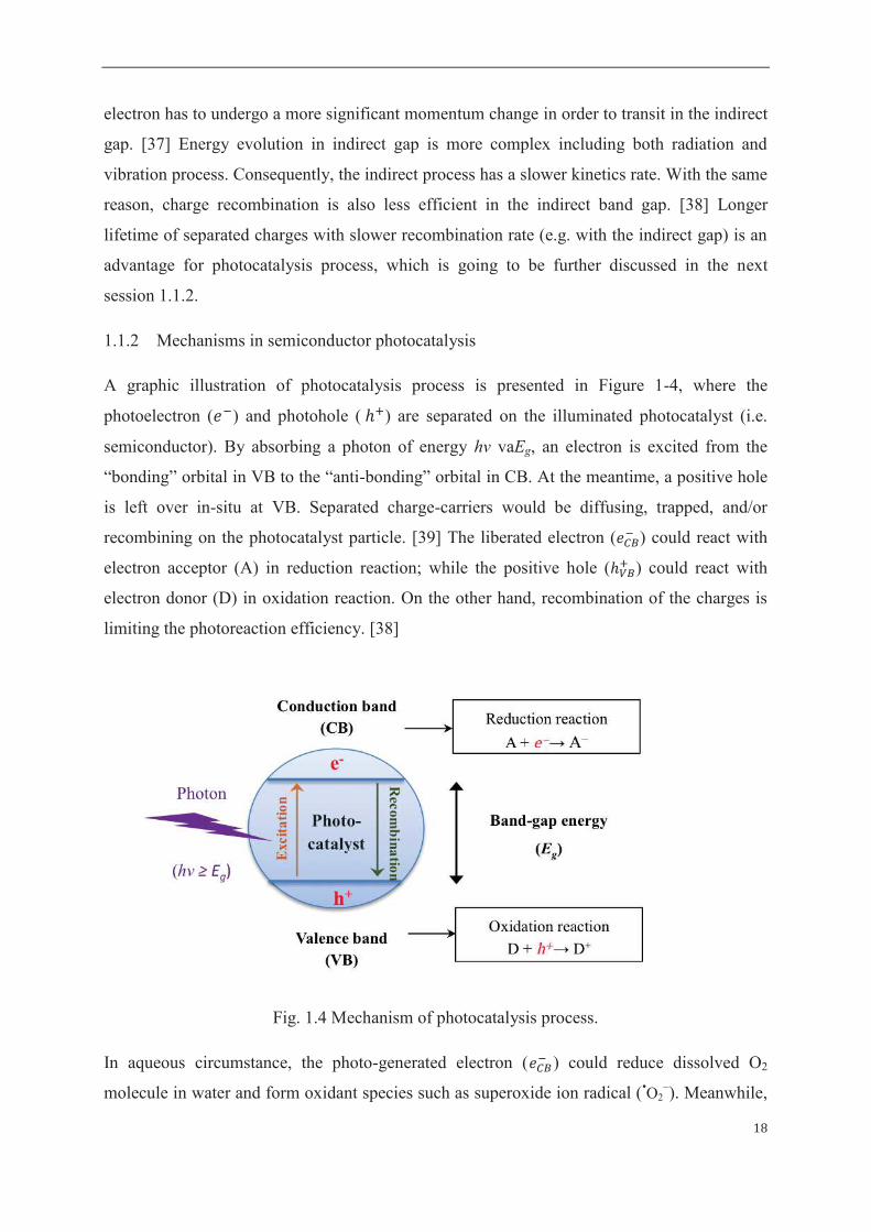
A graphic illustration of photocatalysis process is presented in Figure 1-4, where the
photoelectron (!") and photohole (#$%) are separated on the illuminated photocatalyst (i.e.
semiconductor). By absorbing a photon of energy hv vaEg, an electron is excited from the
“bonding” orbital in VB to the “anti-bonding” orbital in CB. At the meantime, a positive hole
is left over in-situ at VB. Separated charge-carriers would be diffusing, trapped, and/or
recombining on the photocatalyst particle. [39] The liberated electron (!()" ) could react with
electron acceptor (A) in reduction reaction; while the positive hole ($/)% ) could react with
electron donor (D) in oxidation reaction. On the other hand, recombination of the charges is
limiting the photoreaction efficiency. [38]
Fig. 1.4 Mechanism of photocatalysis process.
In aqueous circumstance, the photo-generated electron (!()" ) could reduce dissolved O2
molecule in water and form oxidant species such as superoxide ion radical (•O2–). Meanwhile,

19
the simultaneously generated positive hole ($/)% ) could oxidize H2O molecule and form
hydroxyl radical (•OH). [40] Radical •OH as one of the strongest oxidizing species has an
oxidizing potential E0 (•OHaq/H2O) = 2.59 V at pH=0. [3] It could oxidize almost all sorts of
organic molecules (sometimes also for inorganic species). Molecular oxidation caused by •OH
radical attack is known as advanced oxidation process (AOP) [2], which will be further
discussed in the session 1.3. Global photochemical reactions catalyzed by illuminated
semiconductor in water (dissolved with ambient oxygen) are written as following:
hν → !()" + $/)% (1-6)
O2 + !()" →•O2– (1-7)
H2O + $/)% →•OH + H+ (1-8)
Lifetime of the separated !()" and $/)% on semiconductor particle is crucial for the
photocatalytic activity. Most of the charge carries recombine themselves sooner or later either
in a radiative or non-radiative (by heat) way. Charge recombination will weaken formation of
hydroxyl radicals (•OH) due to less detached charges. Tracing !()" and $/)% formation,
transfer, capture and recombination has been studied with various time-resolved spectroscopy
techniques and the results on their lifetimes are summarized in a review by Fujishima et al in
2008. [38] Trapped electrons and holes absorb light in the visible and near-infrared spectra
[41, 42], whereas free electrons absorb in the infrared or microwave regions [43, 44]. Optical
absorbance by the charge carriers has been recorded by means of transient absorption (TA)
[41], transient diffuse reflectance (TDR) spectroscopies [45], as well as time-resolved
microwave conductivity (TRMC) [43]. After all, !" and #$%# involved in photocatalysis
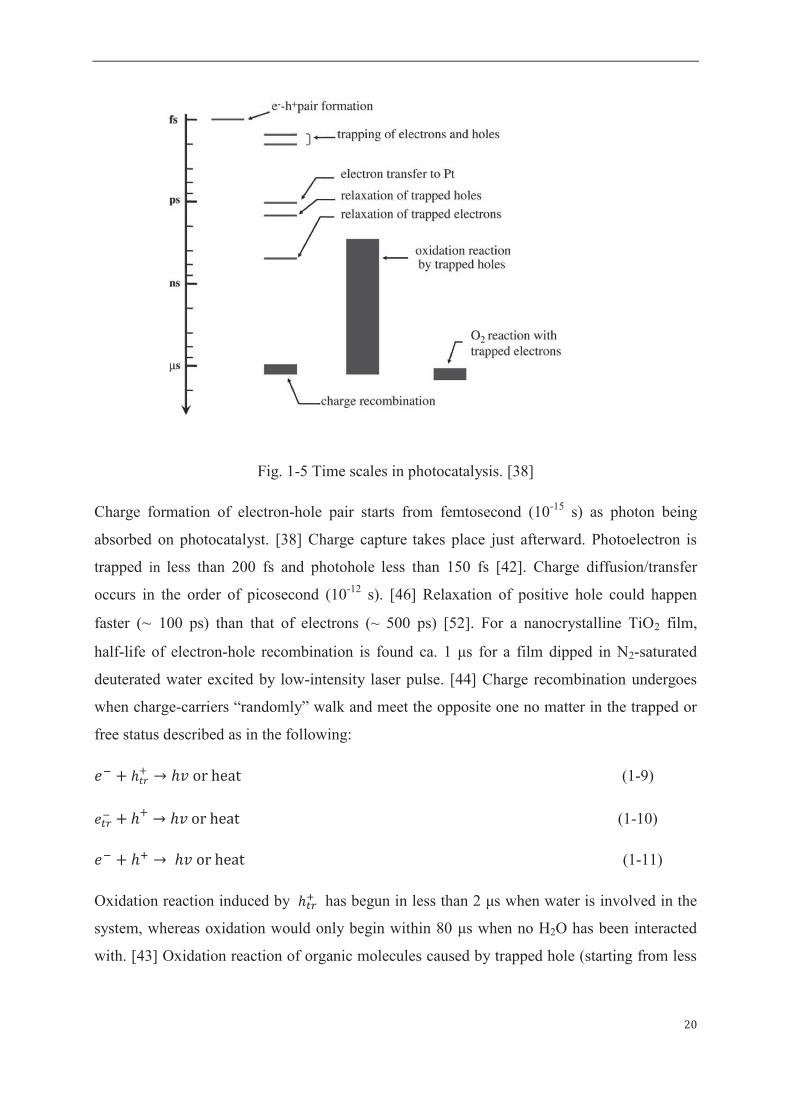
process have been accurately measured in their different states. Conclusive timescale
indication is illustrated in Figure 1-5 with collective results of studying TiO2 samples in
different forms of film and powder. [38] In general, photo-generated !" and#$% have
experienced from femtosecond (10-15 s) as formation until microsecond (10-6 s) as
recombination according to those studied samples.
20
Fig. 1-5 Time scales in photocatalysis. [38]
Charge formation of electron-hole pair starts from femtosecond (10-15 s) as photon being
absorbed on photocatalyst. [38] Charge capture takes place just afterward. Photoelectron is
trapped in less than 200 fs and photohole less than 150 fs [42]. Charge diffusion/transfer
occurs in the order of picosecond (10-12 s). [46] Relaxation of positive hole could happen
faster (~ 100 ps) than that of electrons (~ 500 ps) [52]. For a nanocrystalline TiO2 film,
half-life of electron-hole recombination is found ca. 1 μs for a film dipped in N2-saturated
deuterated water excited by low-intensity laser pulse. [44] Charge recombination undergoes
when charge-carriers “randomly” walk and meet the opposite one no matter in the trapped or
free status described as in the following:
!" : $;<: > $2#or#heat (1-9)
!?@" : $: > $2#or#heat (1-10)
!" : $% > #$2#or#heat (1-11)
Oxidation reaction induced by $?@% has begun in less than 2 μs when water is involved in the
system, whereas oxidation would only begin within 80 μs when no H2O has been interacted
with. [43] Oxidation reaction of organic molecules caused by trapped hole (starting from less

21
than ns) and reduction reaction of O2 caused by trapped electrons (in a few μs) are also
indicated in the time line of Figure 1-5.
Charge capture on semiconductor particle is an essential step for photocatalytic performance.
It suppresses recombination and assists interfacial charge transfer leading to larger amount of
“hot” !" and #$% could sustain in the solid material. In some electron paramagnetic
resonance (EPR) study on illuminated TiO2 particles, trapped electrons have been found in the
form of Ti3+, at the meantime, O2 adsorption on surface has caused Ti3+ signal decayed. [47,
48] Trapped holes have been observed in more complex and deeply scavenged states. For
instance, surface hydroxyl (Ti–•O–Ti–OH), surface oxygen radicals (Ti–O–Ti–•O) and lattice
oxygen radical ion (•O–) are proposed as the sites where positive holes could be confined. [47,
48] In other studies, two types of surface hydroxyl groups as Ti4+–•OH radicals (hole trapping)
and Ti3+–OH groups (electron trapping) have been investigated both by experiments and
theoretical calculations. [49] A density functional theory (DFT) study on hydroxylated TiO2
surface demonstrated an electron-trapping nature of Ti–OH bridges on crystal faces. [50]
Such theoretical result is consistent with an experimental work of Henderson et al [51].
Fig. 1-6 Process occurring on bare TiO2 particle after UV excitation. [38]
Process occurring on bare TiO2 particle after UV excitation is shown in Figure 1-6: radical •OH being formed from $?@% reacting with H2O or !?@" reacting with H2O2. Generation of •OH
radical from H2O has been understood in various possible pathways. Some have found that •OH is formed from $%#interacting with H2O or with absorbed OH– ion. [52, 53] Some others

22
have proposed an alternative way: •OH is produced on surface lattice oxygen (hole trapping
site) where H2O experiences nucleophilic attack [54, 55].
The most commonly accepted mechanism of photocatalytic oxidation is hydroxyl radical
(•OH) attack [56]; however, some studies suggest that the role of radical is probably
overestimated (in another word, primary oxidation is proposed be initiated by free or trapped
holes) [57, 58]. In a study on methanol, both oxidation routes through •OH and $% were
proven to result in the same product formaldehyde [59]:
By •OH radical:
CH3OH + •OH ® •CH2OH + H2O (1-12)
•CH2OH → HCHO + H+ + !" (1-13)
By trapped hole:
CH3OH + $% + OH- → •CH2OH + H2O (1-14)
•CH2OH → HCHO + H+ + !" (1-15)
In addition to the •OH radical, positive hole ($%), superoxide radical ion (•O2–) and singlet
state oxygen (1O2) are also involved as oxidant species in photocatalysis process. Superoxide
radical ion (•O2–) is less often found to trigger oxidation of organic compound in comparison
with •OH and $%. Yet •O2– is easily transferred to •OH by interacting with !" and H+ leading
to contribution to photocatalytic efficiency. [60] Moreover, singlet oxygen 1O2, a strong
oxidant, is proposed being formed by reaction between •O2– and trapped hole, which has been
only recently detected with near-IR phosphorescence in a TiO2 suspension system. [61]
Lifetime of 1O2 is determined close to 2 μs rather shorter than that of •OH ca. 10 μs and
trapped holes, possibly due to faster deactivation of O2 at TiO2 surface.
General factors impacting a heterogeneous photocatalysis process include 1) photocatalyst, 2)
light, 3) dissolved oxygen in water, 4) organic containments in water and 5) temperature.
Catalyst having large surface area can provide more active sites in adsorption and reaction
process. Recombination rate could be reduced due to increase of specific surface area and
removal of structural defects in a study of photocatalytic oxidation of phenol compound. [23]
Excessive catalyst loading (can create a light screening effect) should be avoided to ensure
efficient photon absorption. [62] UV irradiation includes UVA (315 – 400 nm i.e. 3,10 – 3.94

23
eV), UVB (280 – 315 nm i.e. 3.94 – 4.43 eV) and UVC (100 – 280 nm i.e. 4.43 – 12.4 eV)
spectra. In most studies, UVA irradiation provides sufficient photonic activation energy to
semiconductor catalyst. [63] In addition, oxygen plays an indispensable role as electron
acceptor in photocatalysis process especially for environmental application. Oxygen promotes
charge splitting as an electron entrapment and develops into active oxygen species including •O2
–, H2O2, 1O2 and etc. [52] It also maintains the oxidant states of photocatalyst (Ti3+ →+Ti4+)
throughout the process. Therefore, maintaining adequate dissolved oxygen in water should
not be neglected in reactor operation. Moreover, diffusion and reaction kinetics of organic
molecules depend on their molecular weight, initial concentration and chemical potential.
Additionally, pH is one important parameter affecting charge on the catalyst particle and
position of valence and conduction bands. [64] On the other hand, reaction temperature is
found to be suitable between 20 °C and 80 °C since lower temperatures would be
thermodynamically disfavored and higher temperatures would accelerate charge
recombination rate. [65]
In a summary of this session, direct and indirect band gap of semiconductor has been
explained regarding to electronic transition process. Lifetime of photo-generated electron and
hole on semiconductor photocatalyst is known by means of time-resolved spectroscopy
techniques. Photocatalysis mechanism is mainly understood through hydroxyl radical •OH
attack and/or trapped hole ($%), whereas superoxide radical (•O2–) and singlet oxygen (1O2)
have been detected in the recent studies. Photocatalytic efficiency can be affected from
photocatalyst, light, oxygen, pH and temperature. Higher photoreaction rate could be
achieved by using catalyst of large specific surface area and mass below saturation level,
using UVA irradiation and using adequate dissolved oxygen in water.
1.2 TiO2 as photocatalytic material
TiO2 is commonly found as white pigment used in paints, constructions, plastic packages and
cosmetics. Once it was observed that paints consisting of “titanium white” went fading under
exposure to sunlight. After years, it has been recognized that the discoloration phenomenon
was caused by oxidation and removal of organic painting component when TiO2 is
illuminated. Lately, it has been further discovered that the atmospheric O2 was reduced on
TiO2 simultaneously when the organic pigment was bleached. A historical view and modern
applications of photoactive TiO2 is discussed in this session.

24
Structure of TiO2 material is important for its photocatalytic activity in terms of crystal
structure (photo-chemical step), nanoparticle size (quatum effect for light efficiency) and
specific surface area (adsorption/desorption step). For instance, amorphous materials are
usually not highly photoactive since the non-regular arrangement of the atoms does not allow
longer lifetime of seprated charges. Very small size of nanocrystals could have quatum effect
when the particle dimension is comparable with Bohr radius and accordingly the band-gap
energy could be shifted. Moreover, high porosity in a thin film has large surface area that
could improve catalytic reaction rate.
1.2.1 Historical overview and up-to-date applications of TiO2
In 1921, Renz at University of Lugano (Switzerland) discovered that TiO2 could be partially
reduced in organic solvent glycerol under illumination [66]. The color of titania turned from
white to dark. They suggested a reaction at that time as:
TiO2 + light > Ti2O3 or TiO (1-16)
In 1938, Goodeve and Kitchener at University College London performed an inspiring
experiment on TiO2 powder that photo-decomposed a dye “chlorazol sky blue” in the air. [67]
They correlated the photoreaction to ultraviolet (UV) light and even pointed out the quantum
efficiency (i.e. the number of dye molecules photo-decomposed against the number of quanta
absorbed) of the catalyst. [68] In the 1950s, production of hydrogen peroxide (H2O2) on
illuminated zinc oxides has been studied, on which Markham (Catholic University of
America, USA) [69] and Stephens et al. (Wayne State University, USA) [70] have
individually carried out the experiments. Yet both of them were focusing on ZnO samples
since no detectable amount of H2O2 has been observed on TiO2 particles in their experiments.
The general reaction was proposed as:
2!" + 2H+ + O2 ® H2O2 (1-17)
Until then an overall mechanism could be abstracted as an organic compound was oxidized
meanwhile ambient oxygen molecule was reduced on illuminated semiconductors.
Reasonably, studies about O2 adsorption on photocatalyst have been followed up to know
more about photocatalysis process. In 1958, Kennedy et al. at University of Edinburgh (UK)
experimented photo-adsorption of O2 on TiO2 and they demonstrated that it was the electron
25
that transferred from TiO2 to surface; adsorbed O2 have reduced the molecular O2. [71] In the
experiment, they used the same dye “chlorazol sky blue” as in the work of Goodeve.
Filimonov at University of Petersburg (Russia) compared photo-activity of ZnO and TiO2 for
oxidizing isopropanol to acetone. [72] It is claimed that the adsorbed O2 was thoroughly
reduced to H2O on TiO2 sample, whereas O2 could merely be reduced to H2O2 on ZnO
sample. This result could explain why the researchers in America could not detect H2O2
release on TiO2 at that time and thus focused analysis on ZnO in the 1950s. Further on in
1964, Kato and Mashio at Kyoto Institute of Technology (Japan) have proved that H2O2 could
also be produced on different TiO2 powders when oxidizing hydrocarbons and alcohol. [73] It
is remarkable that they concluded that the anatase form of TiO2 powder showed higher
activity than the rutile form.
In McLintock and Ritchie’s study at University of Edinburgh (UK), superoxide radical ion
(•O2–) has been found on TiO2 particle when oxidizing ethylene and propylene. [74] In their
experiment, they observed a complete oxidation of ethylene and propylene into products CO2
and H2O. The radical ion •O2– was produced from oxygen as proposed in equation below:
!" + O2 ® •O2– (1-18)
Honda and Fujishima (Honda’s Ph.D. student at that time) at University of Tokyo (Japan)
have made a breaking-through experiment on TiO2 photo-electrode in 1972. [4]
Photo-electrochemical cell was constructed and single TiO2 crystal was used as an electrode
for water splitting. They found that oxygen was generated on TiO2 electrode (illuminated with
visible light) and hydrogen was produced on Pt electrode without applying external voltage.
Afterwards, a great amount of research work has been devoted to study on producing H2 from
water through illuminated TiO2.
The first time that TiO2 being used to photodegrade pollutants in water treatment was reported
by Frank and Bard at University of Texas (USA) in 1977. [75, 76] They applied TiO2 under
irradiation and oxidized cyanide (CN-) and sulfite (SO3-) into cyanate (OCN-) and sulfate
(SO4-) respectively. Other semiconductors including ZnO, CdS, Fe2O3 and WO3 have been
also experimented. In addition, they anticipated that it is also possible to use TiO2 to
decompose organic substance in addition to the tested inorganic species.

26
Up-to-date applications of photoactive TiO2 have developed in domains including air
purification [77-79], liquid purification [11, 38, 80, 81] and sterilization [9, 82]. Published
documents on “TiO2 photocatalysis for environmental purification” experienced different
growing booms in terms of papers and patents since 1995 as shown in Appendix 1. In
scientific papers, the field on water purification went through a faster growth in comparison
with air purification from 1995 to 2007. However, it is the contrast for the accepted patents in
the same period, that is, air purification had a more robust growth. Technical bottleneck on
filtrating and recycling catalyst particles in liquid phase is the main reason for the difference.
Manufacturing large-scale TiO2 water purifier is the crucial point to link science research to
market exploration.
An example of TiO2 photocatalysis application in field of water purification is displayed in
Figure 1-7. [40] The consecutive system is devoted to treat relatively large volume of water
kept at low energy consumption. The electrolysis- and photocatalysis-treatment system is
composed of boron-doped diamond (BDD) electrode and TiO2 photocatalyst in the individual
unit. High-level wastewater passed through a pre-filter and circulated in an electrolysis unit
containing the BDD electrode. Then the water source was converted into low-level
wastewater, which was continually circulated in a photocatalysis unit. The photoreactor was
packed with TiO2 coated quartz tubes under the sunlight. In the last step, the wastewater was
flowing into a final-filter and ion exchange filter unit. All the electricity power was supplied
from solar energy through the photovoltaic cells in this work, which is another attractive
characteristic of this system.
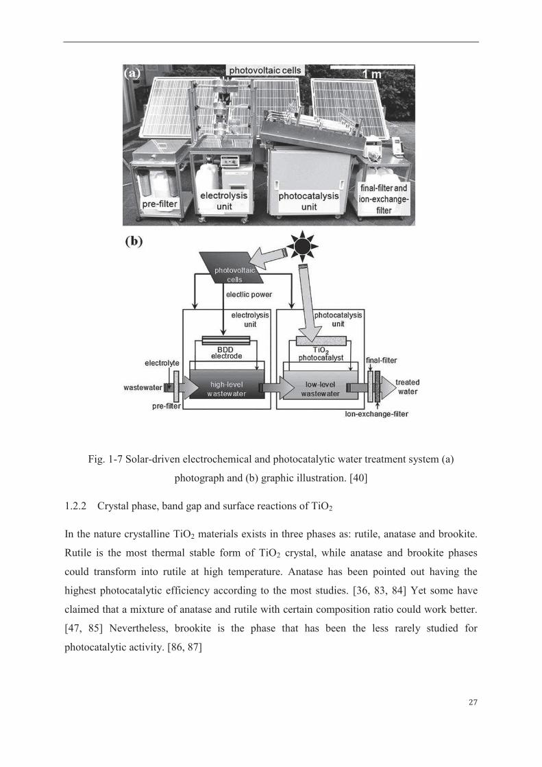
27
Fig. 1-7 Solar-driven electrochemical and photocatalytic water treatment system (a)
photograph and (b) graphic illustration. [40]
1.2.2 Crystal phase, band gap and surface reactions of TiO2
In the nature crystalline TiO2 materials exists in three phases as: rutile, anatase and brookite.
Rutile is the most thermal stable form of TiO2 crystal, while anatase and brookite phases
could transform into rutile at high temperature. Anatase has been pointed out having the
highest photocatalytic efficiency according to the most studies. [36, 83, 84] Yet some have
claimed that a mixture of anatase and rutile with certain composition ratio could work better.
[47, 85] Nevertheless, brookite is the phase that has been the less rarely studied for
photocatalytic activity. [86, 87]
28
Band gap (Eg) of anatase, rutile and brookite differs depending on the crystal structures and
electronic band edges. It is one of the reasons that the specific TiO2 crystal phase has different
photocatalytic efficiency. Anatase is a common phase obtained from sol-gel and chemical
deposition synthesis. Rutile structure would be usually developed when TiO2 is annealed
more than 700 °C. Pure brookite without the other two phases is difficult to prepare and it
could be sometimes observed as a by-product in acidic-medium and low-temperature
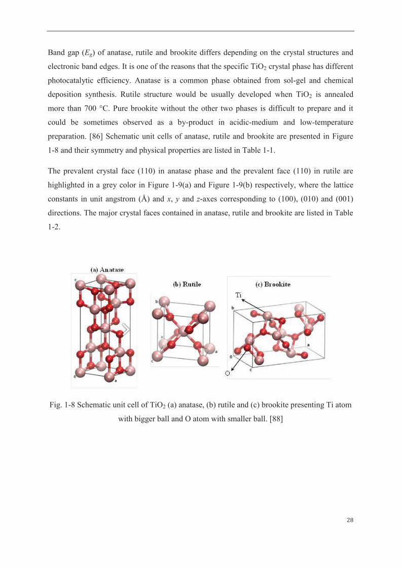
preparation. [86] Schematic unit cells of anatase, rutile and brookite are presented in Figure
1-8 and their symmetry and physical properties are listed in Table 1-1.
The prevalent crystal face (110) in anatase phase and the prevalent face (110) in rutile are
highlighted in a grey color in Figure 1-9(a) and Figure 1-9(b) respectively, where the lattice
constants in unit angstrom (Å) and x, y and z-axes corresponding to (100), (010) and (001)
directions. The major crystal faces contained in anatase, rutile and brookite are listed in Table
1-2.
Fig. 1-8 Schematic unit cell of TiO2 (a) anatase, (b) rutile and (c) brookite presenting Ti atom
with bigger ball and O atom with smaller ball. [88]

29
Table 1-1 Unit cell indices and physical properties of TiO2 anatase, rutile and brookite. [36,
83]
Fig. 1-9 Schematic crystal faces of TiO2 with Ti (white color) and O (red color) atoms and
lattice length in Å: (a) the anatase (101) surface and (b) the rutile (110) surface. [89]
Crystal phase Anatase Rutile Brookite
Molecular formula TiO2 TiO2 TiO2
Formula weight (g mol-1) 79.89 79.89 79.89
Z
(formula units per unit cell)
4
2
8
Crystal system
Point group
Space group
Tetragonal
4/mmm
I41/amd
Tetragonal
4/mmm
P42/mnm
Orthorhombic
mmm
Pbca
Unit cell a (Å) b (Å) c (Å)
Volume (Å3)
3.784 3.784 9.514 136.25
4.585 4.585 2.953 62.07
9.184 5.447 5.145 257.38
Molar volume (cm3 mol-1) 20.156 18.693 19.377
Density (g cm-3) 3.895 4.274 4.123
Refractive index (n0) 2.609 2.488 2.583

30
Table 1-2 Main crystal faces of TiO2 anatase, rutile and brookite. [36, 89, 90]
Anatase has three main faces (101), (001) and (100), among which the first two faces are low
in energy and thermally stable. [91, 92] Surface (101) is the most commonly observed one in
anatase material. Surface (001) can undergo a 4-folded reconstruction so that (004) can be
usually observed in XRD analysis on anatase phase. [91, 93] Similarly surface (100) can
undergo a 2-folded reconstruction into (200), which is more often detected in rod-like anatase.
[93] In the bulk structure, anatase has Ti atom as 6-coordinating, while O atom bonding with
three Ti atoms. On the surface (101) there are rows of bridging oxygen (just connecting two
Ti atoms) and rows of 5-coordinated Ti atoms. [94] The exposed Ti atoms are low in electron
density acting as Lewis acid sites. Schematic graphs and SEM images of anatase single
crystal are exhibited in Figure 1-10 with surfaces (001) and (101) being pointed out. [95]
Fig. 1-10 Anatase TiO2 crystals with a predominance of low index facets: Schematic (A) and
SEM images (B-D) of anatase TiO2 single crystals with different percentages of (001), (101),
and (010) facets. [95]
Crystal phase Anatase Rutile Brookite
Main crystal faces (101)
(001)
(100)
(110)
(100)
(001)
(100)
(110)
(010)

31
Rutile has three major crystal faces as (110), (100) and (001) with the first two surfaces low in
energy. [96] Surface (110) is most thermally stable and has rows of bridging oxygen with
alternating 5-coordinate Ti atoms running parallel on oxygen row as schematically presented
in Figure 1-11. [38] The red rectangle framed (O-Ti4+-O) is active site for water adsorption,
electron transfer and proton transfer. The blue rectangle included bridging oxygen is
responsible for electron and proton transfer. The green rectangle of (Ti4+-O-Ti4+) is available
for oxygen-oxygen coupling and desorption. Surface (100) has similar rows of bridging
oxygen and alternating Ti atoms in a different geometric relationship.
Brookite includes major crystal faces (100), (110) and (010) whose thermal stability reduces
along in the order. [97] As mentioned previously, brookite is more difficult to synthesize in its
pure form and is less studied as a catalyst.
Fig. 1-11 Schematic top view of the rutile (110) surface with bridging oxygen and
5-coordinated Ti atoms: colored rectangle (blue, red and green) responsible for various
possible interactions. [38]
General photocatalytic reactions over TiO2 particle include: 1) electron scavenger (e.g. Ti3+)
interacting with surface adsorbed oxygen and forming superoxide radical ion (•O2–) and 2)
hole scavenger (e.g. lattice oxygen) interacting with adsorbed water and forming hydroxyl
radical (•OH). Hydroxyl radical •OH, superoxide ion •O2– and trapped hole $% could all
possibly degrade aqueous organic compounds (R) through intermediate reactions to the
mineralized products as CO2 and H2O. [33]
TiO2 surface reaction:
Ti (IV) + !" → Ti (III) (1-19)

32
Ti (III) + O2 → Ti (IV) + •O2– (1-20)
H2O + $% → •OH + H+ (1-21)
Degradation of organic molecules (R):
R + •OH → …→ Intermediates → …→ CO2 + H2O (1-22)
R + •O2– → …→ Intermediates → …→ CO2 + H2O (1-23)
R + $% + •O2– → …→ Intermediates → …→ CO2 + H2O (1-24)
Band gap energy (Eg) of TiO2 is the energy difference between its valance band maximal level
(VBM) and conduction band minimal level (CBM). The concept of direct and indirect Eg has
been explained in details in the previous session 1.1. TiO2 anatase of indirect band gap and
rutile of direct band gap are presented in Figure 1-12(a) and 1-12(b), respectively. [36]
Fig. 1-12 Indirect band gap of (a) anatase and direct band gap of (b) rutile. [36]
The outer electron orbitals of Ti and O atoms are given as below:
Ti: 3s2 3p6 3d2 4s2
O: 2s2 2p4

33
The “bonding” valence band in TiO2 consists of hybridization of Ti 3d and O 2p states. The
“anti-bonding” conduction band contains electrons mainly from Ti 3d state (with a few O 2p
state and Ti 3p state). [36] Energy is dissipating through thermal vibration via “phonon”
particles and/or irradiation via particle “photon” particles during charges relaxation and
recombination processes. Indirect transition requires more change of momentum and thus
charge recombination rate is slower in anatase (indirect transition) than that of rutile (direct
transition). It is considered as one reason that anatase could usually perform better
photocatalytic efficiency than rutile does.
Band gap energy (Eg) of TiO2 depends on crystal phase, composite purity and structural
properties and the relevant values have been experimentally and theoretically studied in many
works. Optical techniques are common used to determine Eg experimentally [34, 98, 99],
whereas molecular orbitals calculation and density function theory (DFT) are often applied to
calculate Eg theoretically [88, 100]. Generally, anatase is commonly reported having Eg as
3.23 eV, rutile 3.02 eV and brookite 3.14 eV. [10] In more recent studies, observed Eg value
of anatase has been reported varying from 3.0 to 3.6 eV (310 – 390 nm) according to
synthetic TiO2 materials from different works. [36, 98, 101, 102]
Utilizing solar energy could greatly reduce the cost of photocatalyzed AOP treatment in
wastewater, however, only 5% of UV energy (required in pure TiO2 photocatalysis process) is
composed in the sunlight. On the other hand, sunlight is especially abundant in some area
where clean water severely lacks (e.g. in the deserts). An example of solar-driven
electrochemical and photocatalytic water treatment system has been presented in Figure 1-7
of session 1.2.1.
Fig. 1-13 Various schematic graphs of possible band gap of pure or modified TiO2 materials
for visible-light photocatalysis process: (a) pure TiO2, (b) non-metal doped TiO2, (c)

34
oxygen-deficient TiO2, (d) midgap energy levels for non-metal doped TiO2 and (e) both
oxygen vacancy and non-metal doped midgap levels are considered. [38]
Narrowing the band gap by doping heteroatoms in TiO2 materials could lead to absorbance
shift from UV to visible light. A graphic mechanism on Eg reduction due to dopant atoms
and/or oxygen deficient is given in Figure 1-13. [38] Either electron acceptor or oxygen
deficient could degrade the minimal energy levels of conduction band as shown in Figure
1-13(c). Meanwhile, electron-donor atoms could upgrade the maximum energy levels of
valence band as shown in Figure 1-13(d). The least band gap would be obtained in a case of
both oxygen vacancy and non-metal dopants are present in the photocatalyst as seen in Figure
1-13(e). As a result, midgap levels reduce the band gap so that solar energy of its visible band
is sufficient to initiate photocatalyzed oxidation reactions.
Fig. 1-14 Homogeneous N doping in Cs0.68Ti1.83O4. The left panel: UV-visible absorption
spectra of (1) homogeneous N doped Cs0.68Ti1.83O4 and (2) surface N doped TiO2. [103]
Doping TiO2 materials with heteroatoms such as non-metal atoms (e.g. N and F) [6, 103-107]
and metal atoms (e.g. W and Ag) [108, 109] has been carried out in several works aimed at
solar harvesting. Dopant TiO2 could sustain a smaller band gap (i.e. larger absorbance
wavelength) when electron acceptor (non-metal atoms as dopant) and electron acceptor (metal
atoms) are incorporated. A comparison between pure TiO2 and nitrogen-dopant TiO2 (either
N is homogeneous in the material or on surface) is presented in Figure 1-14 as an example.

35
[103] Apparent absorbance shift to the visible spectrum has been witnessed on the N-dopant
TiO2 sample.
1.3 TiO2 photocatalytic membrane reactors (PMRs)
Photocatalyzed oxidation initiated by photo-generated •OH radical and/or trapped holes is
clarified as an innovative technology of advanced oxidation processes (AOPs). Since concept
of AOPs was first stated in 1987 by Glaze and et al. [2], there are about 500 industrial-scale
AOP plants all over the world today. Photocatalyzed AOP operation using TiO2/UV/O2
reduces the process cost by replacing the expensive oxidant reagents H2O2 and O3 with
ambient oxygen. Integration of photocatalytic oxidation with membrane process is essential
for industry-scale application of PMRs in wastewater treatment filed.
1.3.1 Advanced oxidation processes (AOPs) for degrading pollutants
Advanced oxidation processes (AOPs) indicate a specific treating technique by decomposing
contaminants in water through •OH oxidation reaction. [2] Some other strong oxygen species
such as •O2–, O3 and H2O2 are also possibly involved in the process. It has been proven that
membrane process coupled with AOP operation can be particularly effective in eliminating
non-degradable pollutants such as aromatics, pesticides, herbicides, volatile organic
compounds (VOCs) and petroleum constituents in wastewater. [12, 110, 111] Proposed routes
on phenol oxidation on illuminated TiO2 (as in •OH radical attack mechanism) are presented
in Figure 1-16 as an example. [112]
A major advantage of AOP treatment is to remove contaminants without bringing any
secondary hazardous substances. And the treatment efficiency relies heavily on in-situ
production of •OH radicals. Hydroxyl radical •OH, one of the strongest oxidant species next to
fluorine, has oxidizing potential E0 (•OHaq/H2O) = 2.59 V at pH=0 [3] making it possible to
oxidize almost all types of organic compound. However, pre-treating the water source is
sometimes needed to ensure reliability of AOP performance considering the chemistry of •OH
radical. For instance bicarbonate ion (HCO3–), which can act as •OH scavenger, should be
wiped away before the AOP procedure. [113]
In conventional homogeneous AOP treatment, •OH radical could be formed by adding ozone
(O3) and/or hydrogen peroxide (H2O2). Common homogenous AOP systems include
photochemical process containing O3/UV or H2O2/UV and catalytical process containing
36
H2O2/Fe2+. More recently, solid semiconductor (Sc) for instance TiO2 photocatalyst is added
in the liquid phase and thus a heterogeneous AOP system is consisting as Sc/O2/UV.
Homogeneous/heterogeneous APO operations with or without irradiation are compared in
Table 1-3. High cost of O3 and H2O2 used in conventional homogeneous AOP treatment is
limiting its industrial application to large-scale water plant.
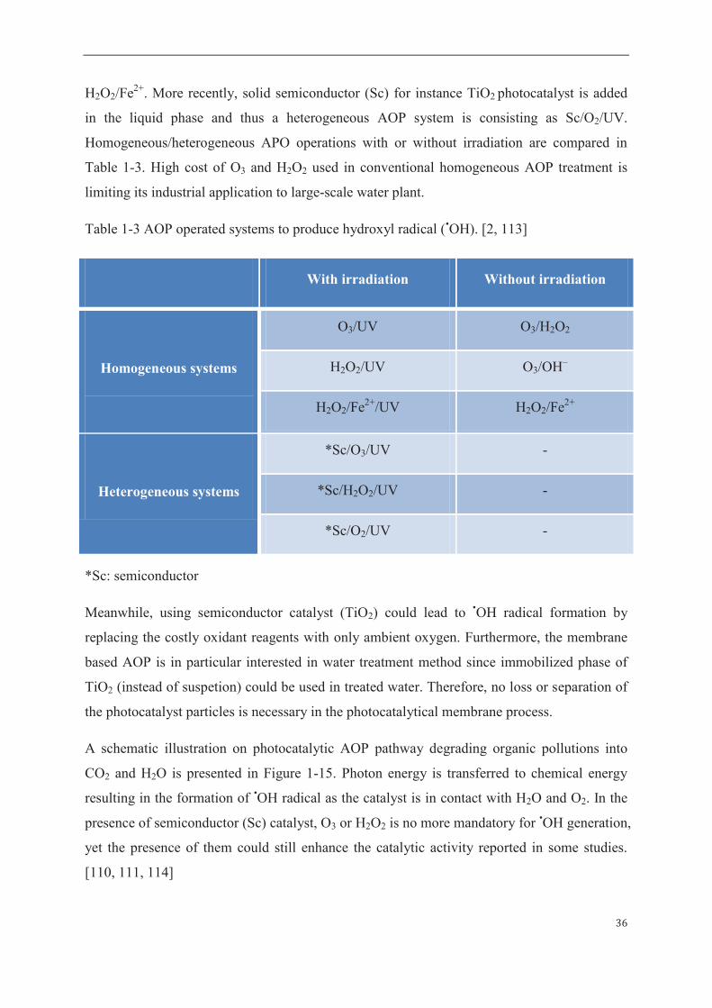
Table 1-3 AOP operated systems to produce hydroxyl radical (•OH). [2, 113]
With irradiation Without irradiation
Homogeneous systems
O3/UV O3/H2O2
H2O2/UV O3/OH–
H2O2/Fe2+/UV H2O2/Fe2+
Heterogeneous systems
*Sc/O3/UV -
*Sc/H2O2/UV -
*Sc/O2/UV -
*Sc: semiconductor
Meanwhile, using semiconductor catalyst (TiO2) could lead to •OH radical formation by
replacing the costly oxidant reagents with only ambient oxygen. Furthermore, the membrane
based AOP is in particular interested in water treatment method since immobilized phase of
TiO2 (instead of suspetion) could be used in treated water. Therefore, no loss or separation of
the photocatalyst particles is necessary in the photocatalytical membrane process.
A schematic illustration on photocatalytic AOP pathway degrading organic pollutions into
CO2 and H2O is presented in Figure 1-15. Photon energy is transferred to chemical energy
resulting in the formation of •OH radical as the catalyst is in contact with H2O and O2. In the
presence of semiconductor (Sc) catalyst, O3 or H2O2 is no more mandatory for •OH generation,
yet the presence of them could still enhance the catalytic activity reported in some studies.
[110, 111, 114]

37
Fig. 1-15 Concept of photocatalytic AOP system (containing Sc/UV/O2) that mineralizes
organic compounds into the end products H2O and CO2.
TiO2 is the most-often applied photocatalyst in current research works. Photocatalytic AOP
system of TiO2/UV/O2 works as effective and economical technique degrading aqueous
organic pollutants for environmental remediation. Proposed photodegradation mechanism of
phenol over illuminated TiO2 (through radical attack) is given as an example in figure 1-16.
Continuous oxidation including aromatic ring opening and carbon bond breaking (through
many intermediate reactions) could lead to mineralization of the organic compound ending in
the final products as water and carbon dioxide.
Fig. 1-16 A possible mechanism of phenol destruction on illuminated TiO2. [112]
Dispersed TiO2 as suspension in solution has been first frequently experimented in many
works. [76, 94, 115] Degussa P25 TiO2 powder (from Evonik) as a “gold standard”
commercial photocatalyst is most commonly used in many laboratory researches. It is a
38
mixture of anatase and rutile in a ratio 80% : 20% in weight. The particles have surface area
ca. 50 m2/g and size less than 25 nm. Both the nature of photocatalyst and conditions in the
solution and irradiation source are found as important parameters for photodegradation
efficiency. However, it is quite often reported that removing TiO2 powders from the treated
liquid flow is very difficult. [38, 40] Filtration is obliged after treatment with catalyst powder
and loss of the catalyst is found to be 30% when recycling reported in one study [59]. It is
indeed the technical “bottleneck” of the suspended system when scaling up it to industrial
application.
Subsequently, a lot of efforts are made on integrating membrane separation and immobilizing
TiO2 particles (e.g. the P25 powders) on mechanical support. In the beginning, TiO2 layers
have been immobilized on glass and silicon supports with methods including sol dip-coating,
physical vapor deposition and chemical vapor deposition. [90, 116, 117] More recently, TiO2
has been coated on membrane substrate and consequently surface reaction and separation
process could be integrated in one photoreactor. [15, 114, 118] Producing porous TiO2
coating layer with large specific surface area is aimed at improving catalytic efficiency in the
immobilized phase.
1.3.2 Membrane separation integrated with photocatalytic AOP treatment
Membrane is a thin and selective barrier through which both matter and energy could pass
under some certain force. Since the 19th century artificial membranes have been attempted and
manufactured for different functions as contactor, distributor and reactor. Artificial
membranes are found in polymers, inorganic composites, ceramics and metals nowadays.
General membrane modules include flat-sheet, spiral wound, tubular and hollow fibers.
Membrane processes are spatially economical, consuming less energy and depleting fewer
less chemicals in continuous and stable performance. They can be found in daily life as
producing clean water, recovering valuable resources, concentrating solutes (e.g. in beverages
and pharmaceutics) and separating gases/vapors.
Driving force indicates the thermodynamic potential on membrane and it contains the
difference in concentration, pressure, temperature and electric potential. Definition of driving
force (F) is given as the ratio between differential potentials against membrane thickness as
written in Equation 1-25.
A = BCD (1-25)

39
where F is driving force, BC is differential potential and δ is membrane thickness.
Concentration-driven membrane have been employed in gas separation (e.g. CO2 capture and
natural gas syntheses), pervaporation (e.g. organic solvent purification), dialysis and osmosis
processes. Pressure-driven membrane processes are categorized according to the applied
pressure (ΔP) as: microfiltration (MF) with ΔP ≤ 2 bar, ultrafiltration (UF) with ΔP = 1 – 10
bar and reverse osmosis (RO) with ΔP = 10 – 25 bar. The components are separated when
they are passing through porous membrane under certain pressure according to components’
molecular sizes. Membrane’s pore sizes are decreasing along with an increased pressure
enforced from MF, UF to RO process so that molecules with smaller size can be separated.
Nanofiltration (NF) is driven with even higher ΔP (15 – 80 bar) and separation mechanism is
based on molecular weight. Moreover, membrane processes driven electrically are often
practiced in electro-dialysis and fuel cells for separating salts and ions.
Mass transfer in the membrane is important to be clarified before scaling up membrane
module. A flux (J) in a membrane is defined as the quantity of a component that is passing
through per unit membrane surface per unit time. The flux is proportional to the driving force
(F) with a proportional factor (A). And by inserting the Equation 1-25 about the driving force,
the flux can be also expressed as in Equation 1-26.
E = F × A = F × BGH (1-26)
where J is flux through membrane, A is proportional factor, F is driving force, BC is
differential potential and δ is membrane thickness.
In earlier researches, TiO2 photocatalysis process has been combined in pressure-driven
membrane processes including MF, UF and RO reported in Ollis’ review in 2003. [11]
Membrane processes were integrated in photoreactor, in the most cases, to filtrate the
dispersed catalyst particles after water treatment. Four types of reactor operation have been
discussed in the review including: 1) photocatalysis (suspension) + MF for catalyst recycle, 2)
photocatalysis (suspension) + UF for catalyst and reactant recycle, 3) photocatalysis (catalyst
immobilized) + UF/RO for reactant recycle and 4) immobilized photocatalyst on UF/RO for
membrane self-cleaning. The author has pointed out that further effort is indeed necessary to
improve the reactor configuration and thus figure out the optimized coupling manner.

40
Coupling photocatalytic oxidation and membrane separation is considered as a very
encouraging prospect in industrial-scale water purification. More recent progress on
photocatalytic membrane reactors (PMRs) has been reviewed in Mozia’s review in 2010. [12]
In addition, pressure-driven NF processes has been studied in photoreactor. Some other
membrane technologies including dialysis, pervaporation (PV) and direct contact membrane
distillation (DCMD) have been also integrated in PMRs for self-cleaning surface function.
Fig. 1-17 Photocatalytic membrane reactors (PMRs) with dispersed catalyst (shown as the
spherical particles) in aqueous solution: (a) photoreactor as the feed tank, (b) photoreactor as
the membrane cell and (c) photoreactor tank between feed and membrane compartments. [12]

41
First of all, the slurry reactor with dispersing catalyst integrated with filtrating membrane is
illustrated in Figure 1-17, in which the photoreactor can be located differently in the loop.
Either the membrane cell can be the photoreactor as shown in Figure 1-17 (a) or the feed tank
can be the photoreactor as shown in Figure 1-17 (b). In a third situation, an additional
reservoir between the feed tank and membrane cell works as the photoreactor as shown in
Figure 1-17 (c). As reported in Mozia’s review, the third configuration has been most often
applied in practice. It could be explained with the feasibility by adding a reservoir without too
much change of the other compartments.
Further on, modified membrane with photocatalytic function provides a new solution for
separation-and-photoreaction coupling. Functionalized membrane works as both contactor
and reactor in the process. Photocatalytic membrane instead of using dispersed catalyst in
liquid phase is presented in Figure 1-18. [12] Such type of PMRs solves the problem of
powder filtration and catalyst loss in the slurry reactor. Yet the reduced surface area and
limited mass transfer could possibly exist as the immobilized phase.
Fig. 1-18 Photocatalytic membrane reactors (PMRs) with immobilized catalyst: (a) on and (b)
in the membrane. [12]
The configuration as shown in Figure 1-18 (a), the photocatalyst coating layer (on the
membrane) is in contact with the feed flow, which has been frequently applied in laboratory
researches. [110, 119-121] The flow direction is from the photoactive side to the non-active
side in this situation. As the light energy is supplied from the feed solution then onto the
catalyst surface, photodegrading reactions take place with the raw organic molecules existing
42
in the feed. As a result, the permeated solution could be composed of water molecules,
products and/or by-products of decomposing reactions, and possibly non-degradable
containments. One advantage of using this membrane asset is that surface fouling can be
reduced since the adsorbed species should be degraded with illuminated photocatalyst layer.
On the other hand, the permeate flux through the membrane could maintain stable due to less
blocking in the pores. For instance, it is found that TiO2-coated and TiO2-entrapped
membranes with enhanced hydrophilicity property have strengthened fouling mitigation. [15,
122] It should be noted that light-transmitting efficiency might be restricted when passing
through a feed solution of high concentration of organic contaminants.
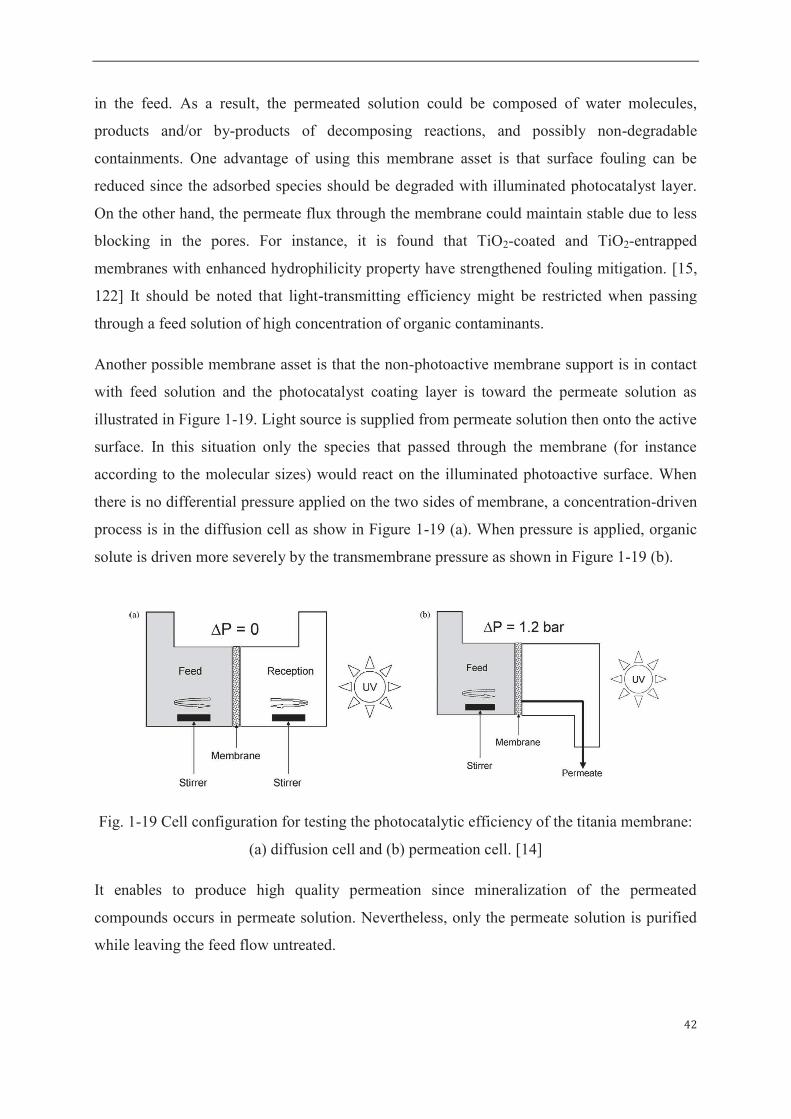
Another possible membrane asset is that the non-photoactive membrane support is in contact
with feed solution and the photocatalyst coating layer is toward the permeate solution as
illustrated in Figure 1-19. Light source is supplied from permeate solution then onto the active
surface. In this situation only the species that passed through the membrane (for instance
according to the molecular sizes) would react on the illuminated photoactive surface. When
there is no differential pressure applied on the two sides of membrane, a concentration-driven
process is in the diffusion cell as show in Figure 1-19 (a). When pressure is applied, organic
solute is driven more severely by the transmembrane pressure as shown in Figure 1-19 (b).
Fig. 1-19 Cell configuration for testing the photocatalytic efficiency of the titania membrane:
(a) diffusion cell and (b) permeation cell. [14]
It enables to produce high quality permeation since mineralization of the permeated
compounds occurs in permeate solution. Nevertheless, only the permeate solution is purified
while leaving the feed flow untreated.
43
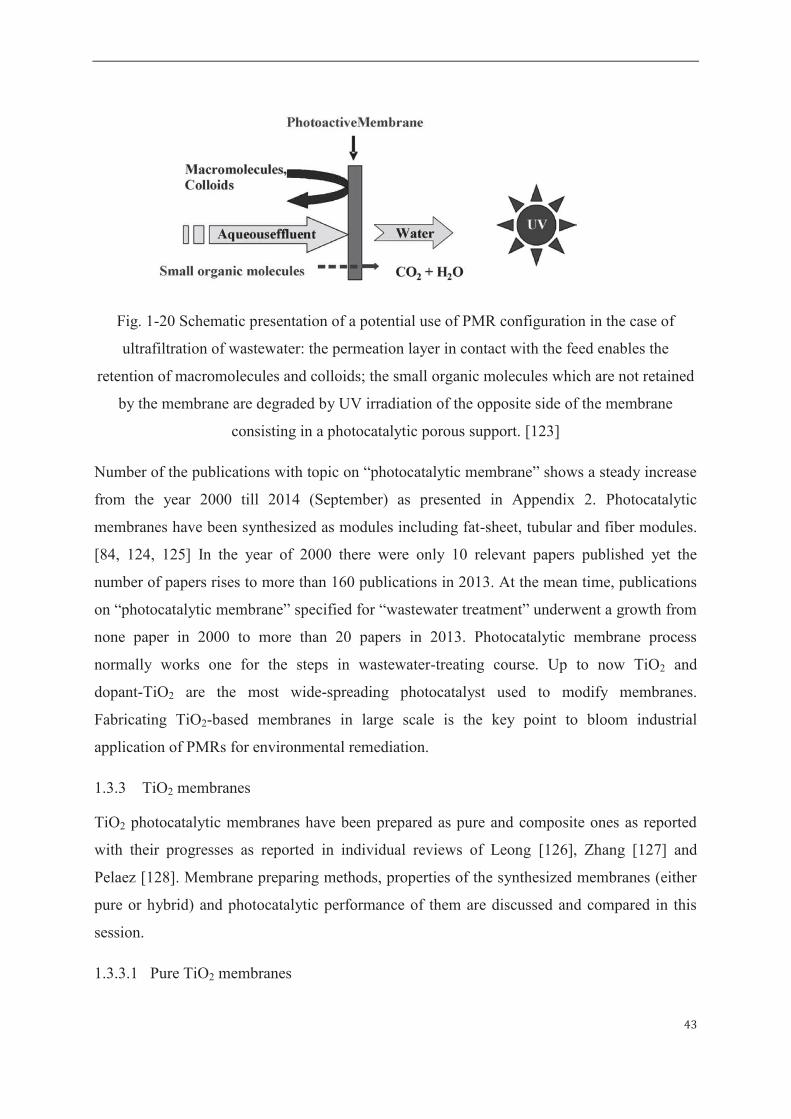
Fig. 1-20 Schematic presentation of a potential use of PMR configuration in the case of
ultrafiltration of wastewater: the permeation layer in contact with the feed enables the
retention of macromolecules and colloids; the small organic molecules which are not retained
by the membrane are degraded by UV irradiation of the opposite side of the membrane
consisting in a photocatalytic porous support. [123]
Number of the publications with topic on “photocatalytic membrane” shows a steady increase
from the year 2000 till 2014 (September) as presented in Appendix 2. Photocatalytic
membranes have been synthesized as modules including fat-sheet, tubular and fiber modules.
[84, 124, 125] In the year of 2000 there were only 10 relevant papers published yet the
number of papers rises to more than 160 publications in 2013. At the mean time, publications
on “photocatalytic membrane” specified for “wastewater treatment” underwent a growth from
none paper in 2000 to more than 20 papers in 2013. Photocatalytic membrane process
normally works one for the steps in wastewater-treating course. Up to now TiO2 and
dopant-TiO2 are the most wide-spreading photocatalyst used to modify membranes.
Fabricating TiO2-based membranes in large scale is the key point to bloom industrial
application of PMRs for environmental remediation.
1.3.3 TiO2 membranes
TiO2 photocatalytic membranes have been prepared as pure and composite ones as reported
with their progresses as reported in individual reviews of Leong [126], Zhang [127] and
Pelaez [128]. Membrane preparing methods, properties of the synthesized membranes (either
pure or hybrid) and photocatalytic performance of them are discussed and compared in this
session.
1.3.3.1 Pure TiO2 membranes
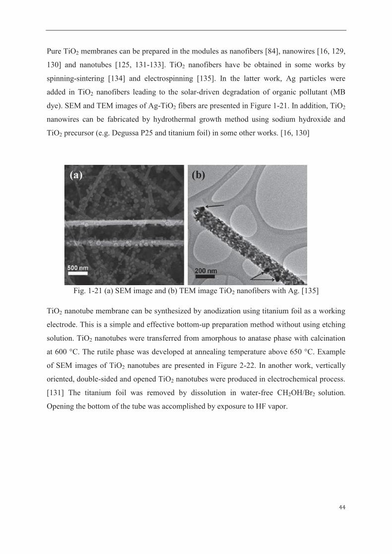
44
Pure TiO2 membranes can be prepared in the modules as nanofibers [84], nanowires [16, 129,
130] and nanotubes [125, 131-133]. TiO2 nanofibers have be obtained in some works by
spinning-sintering [134] and electrospinning [135]. In the latter work, Ag particles were
added in TiO2 nanofibers leading to the solar-driven degradation of organic pollutant (MB
dye). SEM and TEM images of Ag-TiO2 fibers are presented in Figure 1-21. In addition, TiO2
nanowires can be fabricated by hydrothermal growth method using sodium hydroxide and
TiO2 precursor (e.g. Degussa P25 and titanium foil) in some other works. [16, 130]
Fig. 1-21 (a) SEM image and (b) TEM image TiO2 nanofibers with Ag. [135]
TiO2 nanotube membrane can be synthesized by anodization using titanium foil as a working
electrode. This is a simple and effective bottom-up preparation method without using etching
solution. TiO2 nanotubes were transferred from amorphous to anatase phase with calcination
at 600 °C. The rutile phase was developed at annealing temperature above 650 °C. Example
of SEM images of TiO2 nanotubes are presented in Figure 2-22. In another work, vertically
oriented, double-sided and opened TiO2 nanotubes were produced in electrochemical process.
[131] The titanium foil was removed by dissolution in water-free CH2OH/Br2 solution.
Opening the bottom of the tube was accomplished by exposure to HF vapor.

45
Fig. 1-22 SEM images of pure TiO2 nanotubes: (a) top view and (b) side view. [131]
1.3.3.2 TiO2-polymer hybrid membranes
Polymeric membranes are the most-popular membrane type and they are often employed in
wastewater treatment. Manufacture of polymeric membranes is a matured technology in
industry in comparison with ceramic, inorganic and metallic ones. Polymer materials
including polyvinylidenefluoride (PVDF), polyethersulfone (PES), polyethylene terephthalate
(PET), polytetrafluoroethylene (PTFE), polyacrylonitrile (PAN), polyester and polyamide
have been used as mechanical support for photocatalyst. TiO2-polymer composite membranes
can be designed in two ways: 1) TiO2 particles immobilized on surface or 2) TiO2 particles
entrapped in polymer pore structure. The first type can be obtained by coating and depositing
approaches and the second one can be prepared by dispersing TiO2 in polymer solution during
membrane casting and then the catalyst is blended in polymer membrane.
In one work on TiO2-coated polymer membrane, PVDF-PEG membrane prepared using
concentration of 12 wt% PVDF and 2 wt% PEG has a high water flux and rejection. [136]
Three-dimensional AFM surface images of the neat PVDF-PEG membrane and the
TiO2-PVDF-PEG composite membrane are displayed in Fig. 1-23. The membrane flux
decreased when the concentration of added TiO2 particles in the range of 0.5 – 0.5 w% and
then the flux increased gradually again with adding TiO2 in the range of 0.5 – 2.0 wt%. It was
explained as larger pores in the membrane could be formed as TiO2 nanoparticles aggregating

46
due to higher concentration. A smoother surface of TiO2 composite membrane is found in
AFM scanning as given in Figure 1-23 (right), which improves the membrane’s antifouling
property. Moreover, UV illuminated TiO2-composite surface photodegraded the foulants in
the applied cross-flow ultrafiltration process and maintained the flux as found in the presented
work.
Fig. 1-23 Three-dimension AFM surface images of PVDF-PEG membrane: the neat
membrane (left) and TiO2 composite membrane (right). [136]
In another work, water flux of PVDF-g-PAA-TiO2 composite membranes decreased with an
increasing concentration of TiO2 in the range of 0.5 – 3.0 wt% in the coating process due to
pore blockage. [15] SEM images of the PVDF-g-PAA-TiO2 composite membranes containing
0.5 wt% and 3.0 wt% TiO2 are presented in Figure 1-24. It clearly shows that more blockage
in the membrane pores at higher coated ratio.
As for TiO2-blended polymer membranes, the addition of TiO2 in casting solution sometimes
could lead to a more porous membrane. [15, 137-139] For instance, cross-sectional SEM
images of TiO2-blended polymer membrane with various TiO2 loaded ratios are presented in
Figure 1-25. [138] Catalyst TiO2 was embedded in PVDF/PES membranes with a weight ratio
equal to 1 wt% and 4 wt% respectively as presented in the figure. It is revealed that when the
TiO2 concentration was increased the hybrid membranes had less porous sub-layer but had
more interconnectivity of sub-layer microvoids. [138] The membrane water flux was reduced
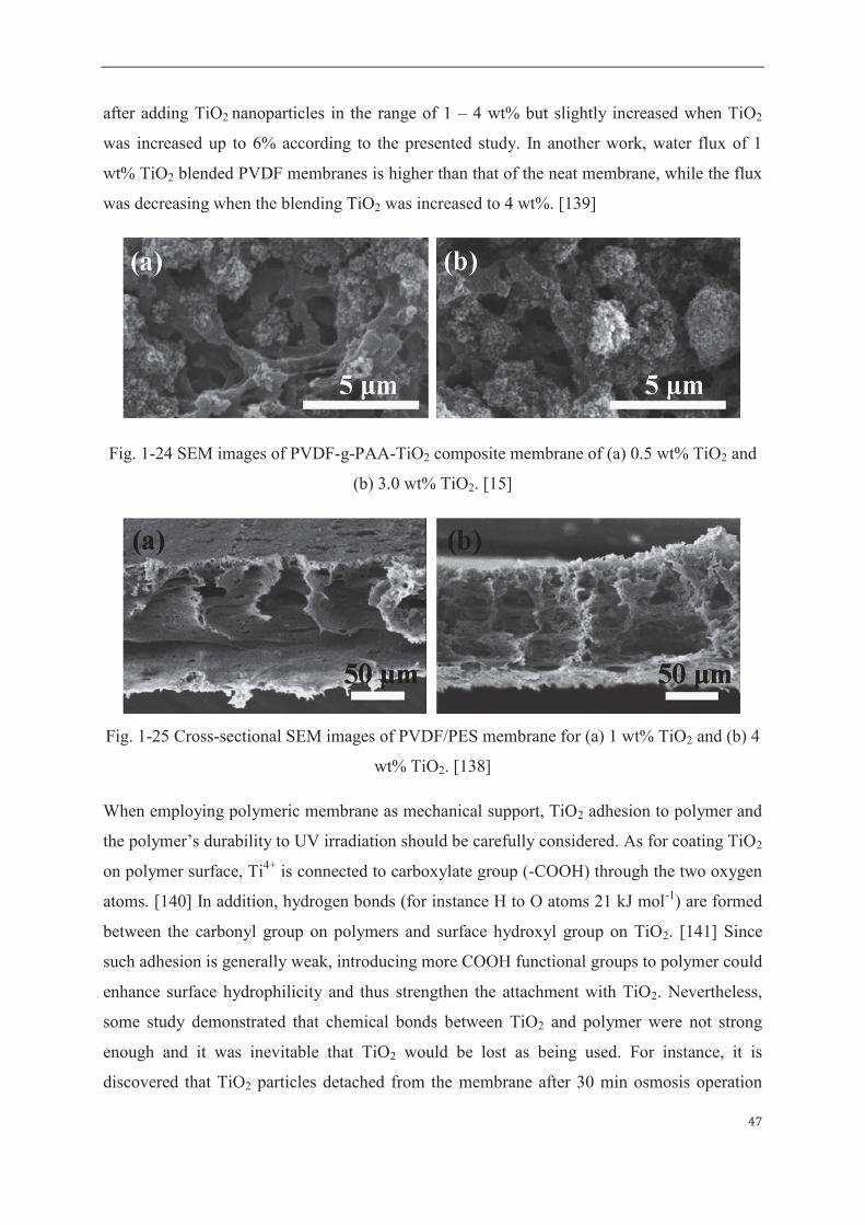
47
after adding TiO2 nanoparticles in the range of 1 – 4 wt% but slightly increased when TiO2
was increased up to 6% according to the presented study. In another work, water flux of 1
wt% TiO2 blended PVDF membranes is higher than that of the neat membrane, while the flux
was decreasing when the blending TiO2 was increased to 4 wt%. [139]
Fig. 1-24 SEM images of PVDF-g-PAA-TiO2 composite membrane of (a) 0.5 wt% TiO2 and
(b) 3.0 wt% TiO2. [15]
Fig. 1-25 Cross-sectional SEM images of PVDF/PES membrane for (a) 1 wt% TiO2 and (b) 4
wt% TiO2. [138]
When employing polymeric membrane as mechanical support, TiO2 adhesion to polymer and
the polymer’s durability to UV irradiation should be carefully considered. As for coating TiO2
on polymer surface, Ti4+ is connected to carboxylate group (-COOH) through the two oxygen
atoms. [140] In addition, hydrogen bonds (for instance H to O atoms 21 kJ mol-1) are formed
between the carbonyl group on polymers and surface hydroxyl group on TiO2. [141] Since
such adhesion is generally weak, introducing more COOH functional groups to polymer could
enhance surface hydrophilicity and thus strengthen the attachment with TiO2. Nevertheless,
some study demonstrated that chemical bonds between TiO2 and polymer were not strong
enough and it was inevitable that TiO2 would be lost as being used. For instance, it is
discovered that TiO2 particles detached from the membrane after 30 min osmosis operation
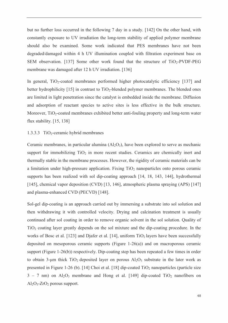
48
but no further loss occurred in the following 7 day in a study. [142] On the other hand, with
constantly exposure to UV irradiation the long-term stability of applied polymer membrane
should also be examined. Some work indicated that PES membranes have not been
degraded/damaged within 4 h UV illumination coupled with filtration experiment base on
SEM observation. [137] Some other work found that the structure of TiO2-PVDF-PEG
membrane was damaged after 12 h UV irradiation. [136]
In general, TiO2-coated membranes performed higher photocatalytic efficiency [137] and
better hydrophilicity [15] in contrast to TiO2-blended polymer membranes. The blended ones
are limited in light penetration since the catalyst is embedded inside the membrane. Diffusion
and adsorption of reactant species to active sites is less effective in the bulk structure.
Moreover, TiO2-coated membranes exhibited better anti-fouling property and long-term water
flux stability. [15, 138]
1.3.3.3 TiO2-ceramic hybrid membranes
Ceramic membranes, in particular alumina (Al2O3), have been explored to serve as mechanic
support for immobilizing TiO2 in more recent studies. Ceramics are chemically inert and
thermally stable in the membrane processes. However, the rigidity of ceramic materials can be
a limitation under high-pressure application. Fixing TiO2 nanoparticles onto porous ceramic
supports has been realized with sol dip-coating approach [14, 18, 143, 144], hydrothermal
[145], chemical vapor deposition (CVD) [13, 146], atmospheric plasma spraying (APS) [147]
and plasma-enhanced CVD (PECVD) [148].
Sol-gel dip-coating is an approach carried out by immersing a substrate into sol solution and
then withdrawing it with controlled velocity. Drying and calcination treatment is usually
continued after sol coating in order to remove organic solvent in the sol solution. Quality of
TiO2 coating layer greatly depends on the sol mixture and the dip-coating procedure. In the
works of Bosc et al. [123] and Djafer et al. [14], uniform TiO2 layers have been successfully
deposited on mesoporous ceramic supports (Figure 1-26(a)) and on macroporous ceramic
support (Figure 1-26(b)) respectively. Dip-coating step has been repeated a few times in order
to obtain 3-μm thick TiO2 deposited layer on porous Al2O3 substrate in the later work as
presented in Figure 1-26 (b). [14] Choi et al. [18] dip-coated TiO2 nanoparticles (particle size
3 – 7 nm) on Al2O3 membrane and Hong et al. [149] dip-coated TiO2 nanofibers on
Al2O3-ZrO2 porous support.
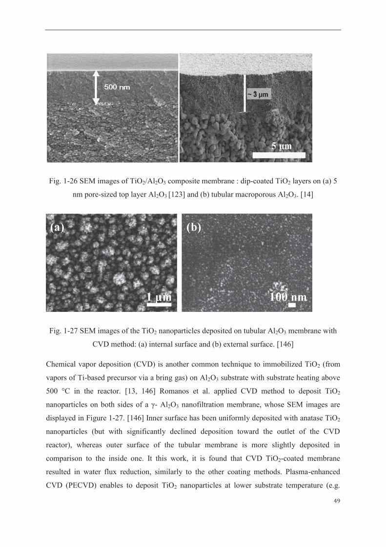
49
Fig. 1-26 SEM images of TiO2/Al2O3 composite membrane : dip-coated TiO2 layers on (a) 5
nm pore-sized top layer Al2O3 [123] and (b) tubular macroporous Al2O3. [14]
Fig. 1-27 SEM images of the TiO2 nanoparticles deposited on tubular Al2O3 membrane with
CVD method: (a) internal surface and (b) external surface. [146]
Chemical vapor deposition (CVD) is another common technique to immobilized TiO2 (from
vapors of Ti-based precursor via a bring gas) on Al2O3 substrate with substrate heating above
500 °C in the reactor. [13, 146] Romanos et al. applied CVD method to deposit TiO2
nanoparticles on both sides of a γ- Al2O3 nanofiltration membrane, whose SEM images are
displayed in Figure 1-27. [146] Inner surface has been uniformly deposited with anatase TiO2
nanoparticles (but with significantly declined deposition toward the outlet of the CVD
reactor), whereas outer surface of the tubular membrane is more slightly deposited in
comparison to the inside one. It this work, it is found that CVD TiO2-coated membrane
resulted in water flux reduction, similarly to the other coating methods. Plasma-enhanced
CVD (PECVD) enables to deposit TiO2 nanoparticles at lower substrate temperature (e.g.
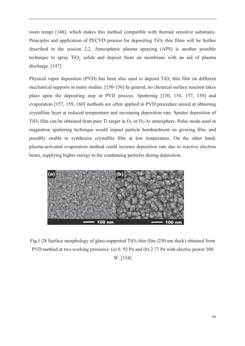
50
room temp) [148], which makes this method compatible with thermal sensitive substrates.
Principles and application of PECVD process for depositing TiO2 thin films will be further
described in the session 2.2. Atmospheric plasma spraying (APS) is another possible
technique to spray TiO2 solids and deposit them on membrane with an aid of plasma
discharge. [147]
Physical vapor deposition (PVD) has been also used to deposit TiO2 thin film on different
mechanical supports in many studies. [150-156] In general, no chemical surface reaction takes
place upon the depositing step in PVD process. Sputtering [150, 154, 157, 158] and
evaporation [157, 159, 160] methods are often applied in PVD procedure aimed at obtaining
crystalline layer at reduced temperature and increasing deposition rate. Sputter deposition of
TiO2 film can be obtained from pure Ti target in O2 or O2/Ar atmosphere. Pulse mode used in
magnetron sputtering technique would impact particle bombardment on growing film, and
possibly enable to synthesize crystallite film at low temperature. On the other hand,
plasma-activated evaporation method could increase deposition rate due to reactive electron
beam, supplying higher energy to the condensing particles during deposition.
Fig.1-28 Surface morphology of glass-supported TiO2 thin film (250 nm thick) obtained from
PVD method at two working pressures: (a) 0. 92 Pa and (b) 2.77 Pa with electric power 300
W. [154]

51
In one study, TiO2 thin films of thickness 250 nm were deposited on glass substrate by
magnetron sputtering PVD. [154] Operating conditions as total working pressure from 0.7 to
3 Pa and substrate temperature equal to 60, 160 and 280°C have been experimented; SEM
images of two samples are displayed in Figure 1-28. Photocatalytic property of the catalyst
films made from different conditions has been compared when degrading methylene blue in
water solution. Anatase crystal face (101) was found in the TiO2 film deposited at substrate
temperature 280°C and its catalytic efficiency (decomposing 80% methylene blue in water
within 100 minutes) is higher with comparison to the samples made at 60 and 160°C.
Fig. 1-29 SEM cross-section (A) and surface (B) images of TiO2 thin film made from PVD
method at 400°C and cross-section (C) and surface (D) images of TiO2 thin film made from
PECVD method at 250°C. [161]
In addition, PVD method using plasma discharge/glancing angle deposition (GLAD)
technique to produce TiO2 with oriented columnar-like structure has been studied. [151, 155,
161] Rotating the substrate at certain angle could vary the particle’s incident angle from the
target to the substrate. Such incident angle variation leads to shadow effect and influences on
nanostructure, crystalline and surface properties of deposited TiO2 thin films. Reversible
transfer between super-hydrophobicity and super-hydrophilicity has been witnessed and it has
been proved that UV illumination greatly improved the surface wetting property [151, 155].
Furthermore, PVD and PECVD prepared TiO2 thin films have been compared in one study
(SEM images presented in Figure 1-29): preferential growth of (004) and (112) crystal
A B
C D
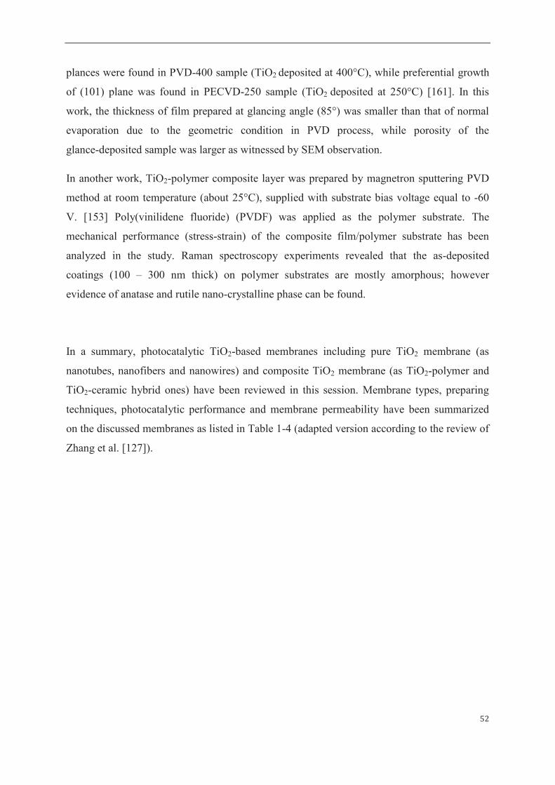
52
plances were found in PVD-400 sample (TiO2 deposited at 400°C), while preferential growth
of (101) plane was found in PECVD-250 sample (TiO2 deposited at 250°C) [161]. In this
work, the thickness of film prepared at glancing angle (85°) was smaller than that of normal
evaporation due to the geometric condition in PVD process, while porosity of the
glance-deposited sample was larger as witnessed by SEM observation.
In another work, TiO2-polymer composite layer was prepared by magnetron sputtering PVD
method at room temperature (about 25°C), supplied with substrate bias voltage equal to -60
V. [153] Poly(vinilidene fluoride) (PVDF) was applied as the polymer substrate. The
mechanical performance (stress-strain) of the composite film/polymer substrate has been
analyzed in the study. Raman spectroscopy experiments revealed that the as-deposited
coatings (100 – 300 nm thick) on polymer substrates are mostly amorphous; however
evidence of anatase and rutile nano-crystalline phase can be found.
In a summary, photocatalytic TiO2-based membranes including pure TiO2 membrane (as
nanotubes, nanofibers and nanowires) and composite TiO2 membrane (as TiO2-polymer and
TiO2-ceramic hybrid ones) have been reviewed in this session. Membrane types, preparing
techniques, photocatalytic performance and membrane permeability have been summarized
on the discussed membranes as listed in Table 1-4 (adapted version according to the review of
Zhang et al. [127]).

Table 1-4 Summary of TiO2-based membranes with their photocatalytic performance and permeability. (adapted from [127])
Note: MB: methylene blue, HA: humic acid, AO7: acid orange 7, RB5: Reactive black 5, MO: methylene orange and DB168: direct black 168.
Membrane types Fabrication method Light source Pollutants Photocatalytic performance
Membrane permeability
Ref
Free-standing TiO2 nanotube membrane
Anodization UV 325, 500 W m-2 MB (6.4 mg L-1) 90% (within 20 h) n.a. [131]
TiO2 nanowire MF membrane
Filtration calcination UV 254, 11 W HA (15 mg L-1) 100% (within 1 h) 3600
(L m-1 h-1 bar-1) [130]
TiO2 nanowire UF membrane
Filtration press-calcination UV 254, 11 W E. coli. (106 CFU
ml-1) 99.9% (within 1 h)
300 – 600 (L m-1 h-1 bar-1)
[129]
TiO2 hollow fiber membrane
Spinning sintering UVA, 32 W AO7 (20 mg L-1) 30–70% (within 1 h) 13.5
(L m-1 h-1 bar-1) [134]
TiO2-PVDF membrane Entrapping UVC, 15 W RB5 > 99% (within 1 h) 50 – 130
(L m-1 h-1, 0.2 bar) [139]
TiO2-CA membrane Filtration UV 254, 400 W m-2 HA 60–70% (within 1 h) 5.3
(L m-1 h-1 bar-1) [162]
TiO2/Al2O3 membrane Sol-gel dip-coating UV 365, 30 W MB (9.6 mg L-1) 100% (within 5 h) 3.5 – 10.4
(L m-2 h-1 bar-1) [18]
TiO2/Al2O3 tube membrane
Chemical vapor deposition (CVD)
UVA, 36 W MO (6.5 mg L-1) 40–80% (within 6 h) 0.6
(L m-2 h-1 bar-1) [146]
TiO2/Al2O3 nanotube membrane
Atmospheric plasma spraying (APS)
UVC, 15 W RB5 (100 mg L-1) 100% (within 1.2 h) 120 – 150
(L m-1 h-1 bar-1) [147]
TiO2/silica nanotube membrane
Sol-gel UV 365, 300 W DB168 (50 mg L-1) 80% (within 3 h) 55 – 65
(L m-2 h-1, 0.5 bar) [143]
Ag-TiO2/HAP /Al2O3 membrane
Sol-gel UV 365, 400W HA (TOC 15 mg L-1) 90% (within 1h) 400 – 1000
(L m-2 h-1, 1 bar) [144]
C, N and Ce co-doped TiO2 membrane
Sol-gel Visible light, 500 W MO (5 mg L-1) 100% (within 2h) 4 – 5
(L m-1 h-1 bar-1) [163]
TiO2/glass Physical vapor deposition
(PVD) UV, 13 W m-2 MB (16 mg L-1) 80% (within 1.5 h) n.a. [154]

1.3.4 Reaction kinetics
Kinetics of photodegradation reaction has been studied with some simple models with respect
to the experimented conditions including membrane asses, solution, dynamic parameters and
so on. The kinetics describes how fast the pollutants are being degraded in the PMR unit. At
the mean time, it can reveal whether the degradation process is reactant dependent or
independent.
Degradation rate is in relevant with mass transfer (in the bulk solution and internal membrane)
and reaction rate (specifically for tested pollutant compound). Some experimental results
showed that photodegradation rate is usually pseudo-first-order [13, 15, 16, 130, 132, 135,
139, 143, 146, 147, 164], which means the rate depends on initial concentration of organic
contaminant but regardless of pollutant type. A few other researches found that
photodegradation rates of phenol [165-167] and dye molecules [168] using TiO2-PE
membranes were zero-order. In such cases, the reaction rate was independent of pollutant
concentration. In the study of Molinari et al. [164], it is revealed that degradation rate of
“patent blue” dye is zero-order when the concentration ≥ 100 mg L-1 and pseudo-first-order
when the concentration ≤ 100 mg L-1. When the initial concentration of organic compound in
feed solution is generally low, a zero-order or first-order kinetics could be applicable
concerning different photodegradation reactors.
Photodegradation rate has been found going up to a plateau as a function of continuous
irradiation time. This phenomenon agrees with Langmuir-Hinshelwood (L-H) reaction
mechanism as described in Equation 1-27. Reaction rate (r) is proportional to surface
coverage (θi) with a reaction constant (kr). Assumptions are presumed when applying L-H
model as 1) the system is in equilibrium, 2) reactions are taking place on surface and 3)
substances competing for active sites are not limiting.
< = . I(I? = J@K+ (1-27)
where r is the degradation rate, C is the concentration of organic compound, kr is the reaction
rate constant and θi is surface coverage
The surface coverage (θ) is dependent on adsorption of reactants onto the surface and
desorption from the surface, with the sorption rates given in Equation 1-28 and Equation 1-29.
<0IL = J0ILMN . KOP (1-28)

55
<IQL = JIQL#K (1-29)
In equilibrium, when the adsorption rate (rads) equals to desorption rate (rdes) as in Equation
1-30, then the coverage ratio (θ) can be obtained as in Equation 1-31.
<0IL = <IQL (1-30)
where rads and rdes are adsorption and desorption rates, kads and kdes are adsorption and
desorption constants, θ is surface coverage and C is the concentration.
K+ = R(S%R( (1-31)
where K is Langmuir adsorption constant as K=kads/kdes.
Therefore
< = J@ R(S%R( (1-32)
where r is the degradation rate, C is the concentration and K is Langmuir adsorption constant.
When the concentration (C) is very low: 1+KC ≈ 1, then the degradation rate is derived to be
in first-order as given in Equation 1-33.
< = . I(I? T J@UP = JVP (1-33)
where k’ is the first-order constant as k’=krK.
With a rearrangement, the pseudo-first-order model can be expressed in Equation 1-34:
ln W ((XY = .JV; (1-34)
Dynamic Langmuir adsorption constant K could be determined with measuring reaction rate
and concentration according to Equation 1-32. By plotting 1/r against 1/C, K parameter could
be known with the linear relationship as in the following Equation 1-35.
S@X =
SZ[ :
SZ[R(X (1-35)
Experimental degradation rate constant k’ (min-1) has been reported in many studies by using
sorts of TiO2 membrane type and model pollutant compounds. The summarized results on the
obtained rate constants by pure TiO2 membrane and TiO2-composite membranes (hybrid with

56
ceramic and polymer ones) are listed in Table 1-5 and Table 1-6 respectively. Test pollutant
model compounds tested in aqueous solution include pharmaceuticals and dye molecules such
as methyl orange (MO), methylene blue (MB), rhodamine B (RB) and reactive black 5 (RB
5), direct black 168 (DB 168) Indigo Carmin (IC) and brilliant green (BG).
Table 1-5 Photocatalytic reaction kinetics of pharmaceuticals and dyes by pure TiO2
membranes.
Membrane type Rate constant, k’
(min-1)
R2 Fabrication
method Pollutant removal Ref
UV-TiO2 nanowires
0.1239
0.0688
0.0430
0.0408
0.0319
0.0422
0.0398
0.0269
0.0277
0.0159
0.0155
0.0008
0.0005
0.999
0.999
0.999
0.995
0.997
0.989
0.999
0.997
0.988
0.993
0.999
0.971
0.945
Hydro- thermal
Norfluoxetine
Atorvastatin
Lincomycin
Fluoxetine
Venlafaxin
Sulfamethoxazole
Diclofenac
Trimethoprim
Bisphenol A
Gemfibrozil
Atrazine
Carbamazepine
Ibuprofen
[169]
UV-TiO2 nanowire membrane
0.022 0.97 - Humic Acid [130]
UV-TiO2 nanotube membrane
0.0001 n.a. - RB [132]
As for pure TiO2 material, the photodegradation rate constant (min-1) was found very
differently depending on the types of pharmaceutical compound in a study using UV
irradiated TiO2 nanowires. [169] The fastest photodegrading rate in the magnitude of order
10-1 min-1 was found for model compounds such as Norfluoxetine, medium rate in the order
of 10-2 min-1 was found for compounds such as Fluoxetine and Bisphenol A, and the slowest
rate in the order of 10-4 min-1 was for compound such as Ibuprofen by the same type of
UV-irradiated TiO2 nanowires (as seen in Table 1-5).

57
Table 1-6 Photocatalytic reaction kinetics of dyes by TiO2-composite membranes.
UV-irradiated membrane type Rate
constant,
k’ (min-1)
R2 Fabrication
method
Pollutant
removal
Ref
UV-H2O2-TiO2-Al2O3
UV-TiO2-Al2O3
UV-H2O2
0.0118
0.0071
0.0043
n.a. Sol-gel dip-coating
DB 168 [143]
UV-TiO2-Al2O3 0.004 n.a. CVD MO [13]
UV-TiO2-α-Al2O3 0.0049 0.999 CVD MO [146]
UV-TiO2-Al2O3 0.076 n.a. APS MB [147]
UV-0.5%TiO2-PVDF-g-PAA
UV-1.5%TiO2-PVDF-g-PAA
UV-3.0%TiO2-PVDF-g-PAA
0.0031
0.0033
0.0042
0.989
0.943
0.988
Self- assembling
RB 5 [15]
UV-TiO2-PVDF 0.0605
0.0986
0.99
0.98 Blending
IC
BG [170]
UV-0%TiO2-PVDF
UV-1%TiO2-PVDF
UV-2%TiO2-PVDF
UV-4%TiO2-PVDF
0.0433
0.0621
0.0634
0.0632
0.956
0.906
0.923
0.952
Blending RB 5 [139]
UV-TiO2-PTFE 0.033a
0.024b n.a. Blending TOCc [171]
UV-TiO2 nanotubes-PU 0.0088 n.a.
Activation reaction
RB [172]
Note: a wavelength 254 nm illumination, b wavelength 185 nm illumination and c TOC: total organic carbon.
As for TiO2-Al2O3 hybrid membranes, some researcher has proved that adding H2O2 in the
reactor resulted in photodegrading rate enhancement of DB 168 dye from 0.0071 min-1 to
0.0118 min-1. [143] Photolysis effect of MB compound by using H2O2 alone with the

58
membrane was measured as k’ = 0.0043 min-1 in the mentioned work, which implies that
adding oxidant reagent H2O2 contributes the photoreaction irrelevant to affect TiO2 surface
reaction. Very close degradation rate of MO dye has been known experimentally as k’ = 0.004
min-1 [13] and k’ = 0.049 min-1 [146] from two individual works using illuminated
TiO2-Al2O3 membranes that have been both prepared with CVD method. Besides,
photodegradation rate of MB dye was found very efficient to be k’ = 0.076 min-1 using
TiO2-Al2O3 membrane synthesized in APS process. [147]
Table 1-7 Photocatalytic reaction kinetics in solar-driven TiO2 disinfection process.
Membrane type Rate constant,
k’ (min-1)
Fabrication
method
Pollutant
removal
Ref
Solar only
TiO2 nanofiber membrane
Solar-TiO2 nanofiber membrane
P25 deposited membrane
Solar-P25 deposited membrane
Ag/TiO2 fiber membrane
Solar-Ag/TiO2 fiber membrane
0.0011
0.0014
0.0100
0.0021
0.0078
0.0171
0.0342
Filtration E. coli 48
As for TiO2-polymer hybrid membranes, some researcher found that faster degradation rate
could be obtained with more TiO2 loaded polymer membranes. In one work, degrading rate
constant (k’ = 0.0042 min-1) of RB 5 dye was obtained with more TiO2 loaded (3.0 wt%)
PVDF-g-PAA membrane than those of less loaded membranes (0.5 and 1.5 wt%). [15]
Similar improvement of reaction kinetics of the same dye (yet k’ is averagely 10 times higher
than that of the previous study) was found in another work using TiO2-blended PVDF
membranes with increased TiO2 concentration from 0 wt% – 2 wt%, but no more reaction
acceleration with continuous loading up to 4 wt%. [139] Moreover, in one study it is
discovered that UV source of larger wavelength 254 nm leads to a faster mineralization rate
indicated by TOC value (k’ = 0.033 min-1) than using smaller wavelength 185 nm (k’ = 0.024
min-1) by the same TiO2-PTEF membrane. [171] By using other dye molecules as IC and BG,
degrading rate by TiO2-PVDF membrane was found higher to be k’ = 0.0605 min-1 and k’ =
0.0986 min-1 respectively in comparison to the work using RB 5 dye. [170]

59
Research work of deactivation E. coli using solar-illuminated TiO2 nanofiber membrane, P25
deposited membrane and Ag/TiO2 fiber membrane is presented in Table 1-7.
1.4 Conclusion
Band gap energy (Eg) is the energy difference between valence band and conduction band in
solid materials. When semiconductor particles absorb photo energy larger than its band gap
energy, radical �OH can be formed due to charge separation of !" and#$%. Photo-generated
�OH (a radical of very high oxidizing potential) can oxide/degrade almost all sorts of organic
pollutants in aqueous solution. The photocatalytic advanced oxidation processes (AOPs) leads
to an innovative water treatment technology. TiO2 is found as an effective photocatalyst since
1972 and then attracts a lot of interest in research work on photocatalysis mechanisms.
Degussa P25 TiO2 powder from Evonik (a mixture of anatase and rutile) serves as the gold
standard photocatalyst in many laboratory studies. Crystalline anatase TiO2 (in the pure form)
is found of the highest photocatalytic efficiency in comparison to the other two phases as
rutile and brookite. Eg of synthesized anatase TiO2 is reported in the range of 3.0 – 3.3 eV
depending on the material preparation methods and characterization methods.
Membrane separation has been recently integrated in TiO2-AOP procedure regarding to
membrane reactor of higher compactness, better integrity and separable feasibility is preferred
to the slurry reactor for industrial-scale use. Great efforts have been made on synthesizing
TiO2-polymer membranes, TiO2-ceramic membranes and TiO2 pure membranes for water
purifying purpose in recent studies. Membrane coated with TiO2 is proven as more effective
and efficient than membrane entrapped with TiO2 since more active sites for reactants and
photons are provided as the catalyst on the surface. Photocatalytic membrane reactors (PMRs)
have been contemplated in variant possible configurations of the photoactive TiO2 layer either
in contact with feed or with permeate solutions. When the catalyst is toward the feed flow,
liquid-solid contact/reaction times can be repeated by circulating the feed but the passed
species through the membrane remains in the permeate solution (if without further treatment).
When the catalyst is toward the permeate flow, mineralization of organic pollutant could be
carried out for the organic species passing through the membrane.

60
2 Plasma-Enhanced Chemical Vapor Deposition (PECVD) for TiO2 membrane manufacture
Since the 50s, PECVD method has been applied in materials processing to deposit inorganic
films especially for solar cell and integrated circuits fabrication. More recently, it has been
implemented for the manufacture of TiO2 films for photocatalytic applications. Principles of
plasma-assisted CVD procedures, focusing on as a low temperature deposition process, will
be first explained in this part. To follow up, some specific examples on preparation of
inorganic and more particularly TiO2 films with PECVD approach will be discussed.
2.1 Generalities on PECVD process
2.1.1 Chemical Vapor Deposition (CVD) methods
Chemical vapor deposition (CVD) is a process where a solid material is deposited from a
precursor vapor with chemical reactions occurring on or in the vicinity of a substrate surface.
[173] Deposited materials can be obtained as coatings, powders or single crystals. In
particular, CVD processes have been widely employed to prepare films of uniform-thickness,
high-purity and high-performance. Produced films may be amorphous, monocrystalline,
polycrystalline, and epitaxial according to the precursor(s) and reactor conditions. In
comparison with physical vapor deposition (PVD) process, CVD has many advantages as 1)
allowing three-dimensional and complete-coverage coating, while PVD is typically line of
sight deposition, 2) CVD using high precursor flow rates leading to higher deposition rates
than that of PVD, 3) ultra-high vacuum is not obliged for CVD and the reactor is relatively
simple to scale up, 4) controlling the stoichiometry more easily by monitoring flow rates of
precursors in CVD than by monitoring evaporation rate in PVD and 5) CVD enables to
fabricate abrupt junctions, which is not the case for PVD.
The CVD process generally comes in different categories as atmospheric pressure CVD
(APCVD), low pressure CVD (LPCVD), plasma-enhanced CVD (PECVD), photon (laser)
induced CVD (PHCVD) and so forth. In thermal CVD processes (e.g. APCVD and LPCVD),
heating is the energy source for the chemical reactions in gas phase and at the gas-solid
interface. In the plasma process (e.g. PECVD), electric power is the energy source to assist
precursor decomposition and high surface temperature is no longer necessary to active the
reactions. Nevertheless, optional heating of substrate can enable to tune the structure of the
prepared solid material; so the substrate temperature is a critical factor in thin film
manufacturing.

61
A comparison between thermal CVD and PECVD methods for depositing inorganic films
such as silicon nitride (SixNy), silicon dioxide (SiO2) and amorphous silicon (α-Si) is
presented in Table 1-8, where the different substrate temperatures required in the processes
are listed.
Table 1-8 Substrate temperature in thermal CVD and PECVD. [173, 174]
Since high deposition temperature (higher than 350°C) is required in thermal CVD processes,
it is unsuitable for thermally sensitive substrate especially for the polymer ones normally not
bearing up to 250°C. This limitation doesn’t systematically occur for PECVD process since
electric field acts as the main energy source for the decomposition of precursor(s).
In PECVD process, vapor molecules are more easily broken up with the bonds due to
ionization and hot electrons. Plasma reactivity enables films to grow at low substrate
temperature (room temp. – 500 °C) with reasonable deposition rate. In addition, low-pressure
plasma (a few mbar) leading surface-kinetics controlled deposition produces films of good
uniformity. Some drawbacks of PECVD process include difficulties in controlling
stoichiometry due to variations in bond strengths of precursors. Moreover, some substrate
surface may potentially be damaged due to ion bombardment occurring in plasma. In terms of
equipment, PECVD (as low-pressure CVD, LPCVD) requires the use of a pumping system to
maintain a low pressure that leads to higher complexity and cost of reactor than in
atmospheric-pressure CVD (APCVD) process. In a summary, advantages and limitation of
thermal CVD process and PECVD approaches are presented in Table 1-9. Their applications
in preparing inorganic films and the relevant process conditions are also given in the table.
Film Precursors Thermal CVD PECVD
Silicon nitride (SixNy) SiH4 and NH3 750 °C 200 – 500 °C
Silicon dioxide (SiO2) SiH4 and O2 350 – 550 °C 200 – 400 °C
Amorphous silicon
(α-Si)
SiH4 550 – 650 °C 200 – 400 °C
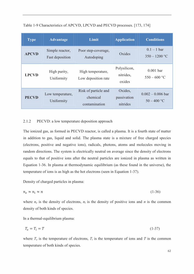
62
Table 1-9 Characteristics of APCVD, LPCVD and PECVD processes. [173, 174]
Type Advantage Limit Application Conditions
APCVD Simple reactor,
Fast deposition
Poor step-coverage,
Autodoping Oxides
0.1 – 1 bar
350 – 1200 °C
LPCVD High purity,
Uniformity
High temperature,
Low deposition rate
Polysilicon,
nitrides,
oxides
0.001 bar
550 – 600 °C
PECVD Low temperature,
Uniformity
Risk of particle and
chemical
contamination
Oxides,
passivation
nitrides
0.002 – 0.006 bar
50 – 400 °C
2.1.2 PECVD: a low temperature deposition approach
The ionized gas, as formed in PECVD reactor, is called a plasma. It is a fourth state of matter
in addition to gas, liquid and solid. The plasma state is a mixture of free charged species
(electrons, positive and negative ions), radicals, photons, atoms and molecules moving in
random directions. The system is electrically neutral on average since the density of electrons
equals to that of positive ions after the neutral particles are ionized in plasma as written in
Equation 1-36. In plasma at thermodynamic equilibrium (as these found in the universe), the
temperature of ions is as high as the hot electrons (seen in Equation 1-37).
Density of charged particles in plasma:
\Q T \+ T \ (1-36)
where ne is the density of electrons, ni is the density of positive ions and n is the common
density of both kinds of species.
In a thermal-equilibrium plasma:
]Q = ]+ = ] (1-37)
where Te is the temperature of electrons, Ti is the temperature of ions and T is the common
temperature of both kinds of species.
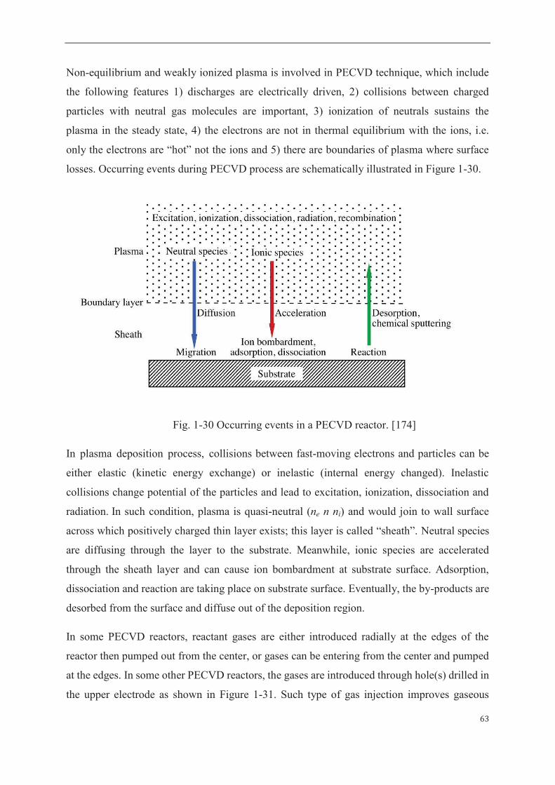
63
Non-equilibrium and weakly ionized plasma is involved in PECVD technique, which include
the following features 1) discharges are electrically driven, 2) collisions between charged
particles with neutral gas molecules are important, 3) ionization of neutrals sustains the
plasma in the steady state, 4) the electrons are not in thermal equilibrium with the ions, i.e.
only the electrons are “hot” not the ions and 5) there are boundaries of plasma where surface
losses. Occurring events during PECVD process are schematically illustrated in Figure 1-30.
Fig. 1-30 Occurring events in a PECVD reactor. [174]
In plasma deposition process, collisions between fast-moving electrons and particles can be
either elastic (kinetic energy exchange) or inelastic (internal energy changed). Inelastic
collisions change potential of the particles and lead to excitation, ionization, dissociation and
radiation. In such condition, plasma is quasi-neutral (ne n ni) and would join to wall surface
across which positively charged thin layer exists; this layer is called “sheath”. Neutral species
are diffusing through the layer to the substrate. Meanwhile, ionic species are accelerated
through the sheath layer and can cause ion bombardment at substrate surface. Adsorption,
dissociation and reaction are taking place on substrate surface. Eventually, the by-products are
desorbed from the surface and diffuse out of the deposition region.
In some PECVD reactors, reactant gases are either introduced radially at the edges of the
reactor then pumped out from the center, or gases can be entering from the center and pumped
at the edges. In some other PECVD reactors, the gases are introduced through hole(s) drilled in
the upper electrode as shown in Figure 1-31. Such type of gas injection improves gaseous

64
molecules distribution. An extended inlet source can be made with more drilled holes as
showerhead-alike as shown in Figure 1-31(b). The modified extension can not only distribute
emitted angles widely but also enlarge the distribution of arrival angle. Substrate wafer is
mounted at the lower electrode that is normally grounded. Sometimes, the substrate is rotated to
randomize its position during processing.
Fig. 1-31 Flux lines of atoms from small area and extended sources: (a) flux lines from a point
or small area with a wide emitted angle distribution but arrow arrival angle distribution and (b)
flux lines from an extended source with a wider arrival angle distribution. [174]
Radio frequency (RF) discharge of 13.65 MHz is commonly employed in the current PECVD
techniques. Power with frequencies faster than 100 kHz will only induce the electrons to
respond to the switching electric field but not the ions. Alternative current (AC) potential at top
and bottom electrodes in RF plasma is presented in Figure 1-32. Plasma exists in the space
between the two electrodes and there is no differential potential in the plasma on average.
RF plasma process is capable of depositing materials even of insulating nature, whereas it is not
the case for direct current (DC) glow discharge in which insulators cannot sustain plasma.
Furthermore, RF plasma avoids accumulating charges on insulators; however, the ion current in
DC plasma would charge the insulator positively and extinguish the plasma eventually.
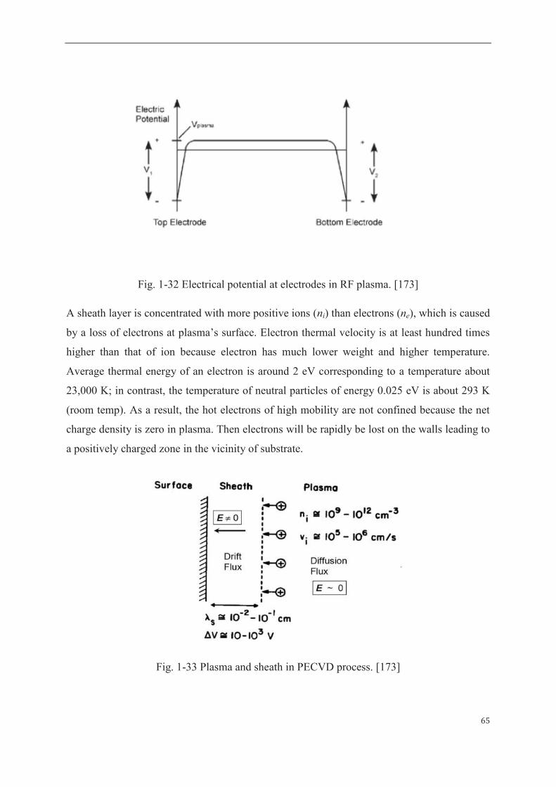
65
Fig. 1-32 Electrical potential at electrodes in RF plasma. [173]
A sheath layer is concentrated with more positive ions (ni) than electrons (ne), which is caused
by a loss of electrons at plasma’s surface. Electron thermal velocity is at least hundred times
higher than that of ion because electron has much lower weight and higher temperature.
Average thermal energy of an electron is around 2 eV corresponding to a temperature about
23,000 K; in contrast, the temperature of neutral particles of energy 0.025 eV is about 293 K
(room temp). As a result, the hot electrons of high mobility are not confined because the net
charge density is zero in plasma. Then electrons will be rapidly be lost on the walls leading to
a positively charged zone in the vicinity of substrate.
Fig. 1-33 Plasma and sheath in PECVD process. [173]

66
Sheath thickness (λs) is typically about 0.01 – 0.1 cm in a plasma. Density of positive ions (ni)
is around 109 – 1012 particles/cm3 and velocity of ions (vi) is around 105 – 106 cm/s in the bulk
plasma. Electric filed (E) is close to zero on average because the number of electrons equals
to the number of ions in the plasma. But in the sheath layer there is a larger density of positive
ions (ni > ne) so that the layer is positively charged. The sheath interface balances the opposite
negative charge on the substrate surface. The electric field (E) in sheath layer is no longer
zero and increases to about 10 – 103 V. Consequently, the electrons would reflect from the
wall (sheath) back to the plasma and the ions would enter and be accelerated through sheath
layer as presented in Figure 1-33.
A number of simulating tools have been developed for simulation of deposition mechanisms
in CVD process. [175] An illustrated graph about fluxes involved in low pressure process is
displayed in Figure 1-34. Mathematical description of the various possible fluxes is clarified
as seen in Equation 1-38. The net flux of particles takes account about the effects from direct
flux of neutrals Fidirect(neutrals), direct flux of ions F
idirect(ions), redeposited fluxes F
iredep (both
from emitted and resputtered particles), flux of diffusion-in Fidiff.in, flux of diffusion-out
Fidiff.out, emitted flux Fi
emmitted and sputtered flux Fisputtered.
Fig. 1-34 Possible fluxes of particles in CVD process. [174]
The net flux of particles in CVD:
(1-38) Fnet
i = Fdirect(neutrals)i +Fdirect (ions)
i +Fredep
i +Fdiff .ini ÿFemitted
i ÿFsputtered
i ÿFdiff .out
i

67
Modeling PECVD system is first based on figuring out the types of fluxes involved in the
electronical-assisted process. A graph of RF PECVD reactor depositing SiO2 films from SiH4
and O2 is illustrated in Figure 1-35 (on the left). The relevant fluxes of ions and neutrals
during deposition are presented in Figure 1-35 (on the right).
Fig. 1-35 PECVD reactor and relevant fluxes in the deposition process. [173]
Direct fluxes of neutrals (Fd) are the main portion in depositing fluxes as the weakly ionized
plasma being involved in PECVD process. Ion-induced fluxes (Fi) are characteristic in plasma
deposition since the ions could enhance particles transporting by collisions. Moreover,
desorbed particles can be emitted and then contribute to redepositing fluxes.

68
Accordingly, deposition rate can be calculated as in Equation 1-39 taking account the
mentioned depositing fluxes in PECVD process.
(1-39)
where sc is the striking coefficient, kd and ki are the relative rate constants for neutrals and
ion-induced components respectively, Fd and Fi are the fluxes of neutrals and ion-induced
components respectively and N is the density of the atoms in the film.
The deposition rate (or film growth rate) in PECVD depends on both substrate temperature
and reactant concentration as shown in Figure 1-36. At high temperatures, plasma deposition
is diffusion controlled, and at low temperatures it is reaction limited. For intermediate
temperatures, competition of gas transport and feed rate determines film-growing kinetics in
which a fast and stable deposition rate can be attained. On the other hand, there is a growing
rate plateau when the reactant concentration is neither too much nor too little; in such
conditions, adequate precursor vapor induced nucleation in gas phase is affecting deposition
process leading to a reasonable film-growing velocity. Usually maximum deposition rates in
the range 0.1 – 100 nm/min can be achieved.
Fig. 1-36 Deposition rate depending on substrate temperature and reactant concentration.
[[173, 174]
rate=sckdFd( )+ kiFi( )
N

69
2.2 PECVD process for the preparation of TiO2 films
Thin film typically indicates a material of thickness less than 1000 nm. Properties of thin
films are different from bulk materials in terms of the non-fully dense and defect structures.
Such quasi-2D materials (very thin thickness) are under stress and strongly influenced by
surface/interface effects and ion bombardment. Increasing ion bombardment tends to make
films denser and cause the film stress to become more compressive. [176] However,
excessive compressive stress can lead to impaired films. In general, quality of a film refers to
physico-chemical (e.g. density and composition), electrical (e.g. breakdown voltage),
mechanical (e.g. stress and adhesion) and optical (e.g. transparency and refractive index)
properties. Defect structure, grain size and orientation in film and impurity level (or doping)
are critical for the film’s performance. Fortunately, films properties and performance can be
adjusted by the optimization of the PECVD parameters, the chamber geometry and the energy
excitation source.
2.2.1 Deposition of inorganic film
PECVD synthesized inorganic films include elements, oxides, nitrides, carbides and borides.
Common inorganic films obtained in PECVD process with corresponding gas sources and
required deposition temperatures are listed in Table 1-10. Typically, amorphous silicon (α-Si)
and crystalline silicon (c-Si) have been deposited from SiH4 + H2 respectively at 300 and 400
°C. Silicon oxide (SiO2) and titanium oxide (TiO2) films have been obtained respectively
from gases SiCl4 + O2 and TiCl4 + O2 respectively at temperatures as low as 100 °C. Silicon
nitride (Si3N4) film has been possibly formed from SiH4 + NH3 + N2 at room temperature 25
°C.
Silicon nitride (SixNy) films are particularly representative of PECVD inorganic materials.
SEM picture of silicon nitride film prepared from SiH4 + NH3 reactant gases by PECVD
method is presented in Figure 1-37. The film is of good conformity, step-coverage, and
homogeneous thickness. A stoichiometry synthesis of Si3N4 from SiH4 +NH3 is written in
equation (1-40). Yet it is often that composition of inexact stoichiometry is obtained in
PECVD films due to different bond strength in precursor molecules, which are experiencing
thermal/plasma decomposition.
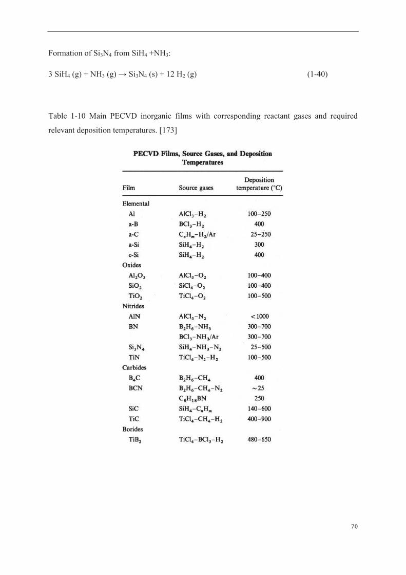
70
Formation of Si3N4 from SiH4 +NH3:
3 SiH4 (g) + NH3 (g) → Si3N4 (s) + 12 H2 (g) (1-40)
Table 1-10 Main PECVD inorganic films with corresponding reactant gases and required
relevant deposition temperatures. [173]

71
Fig. 1-37 Conformal step coverage of PECVD SixNy film. [177]
Silicon nitride (SixNy) films produced IN APCVD, LPCVD and PECVD processes from gas
mixture SiH4 + NH3 are compared in terms of the films’ physical and chemical properties as
given in Table 1-11. Film of Si3N4 has been deposited at 900 °C by APCVD, hydrogenated
Si3N4(H) has been deposited by 750 °C in LPCVD and SixNy has been deposited at 300 °C by
PECVD. Process temperature has been reduced by 600 °C and 450°C in PECVD compared to
APCVD and LPCVD, respectively. It can be seen that PECVD film has a lower density,
better conformity and higher water permeability.
In the presented examples as shown in Table 1-11, a more compressive PECVD silicon
nitride film is obtained due to ion bombardment effect as the energetic ions being accelerated
through a sheath layer from plasma toward substrate. Definition of film stress (σ) is given in
Equation 1-41. The film stress is depending on film thickness, substrate thickness, position in
the film and Young’s modulus of materials. Different film stress could be formed in different
interfaces.
Thin film stress σ:
_̂ = ?`8bcd fg?i?`j
k: m 8`8i
p`?`q (1-41)
where -1/2 < Yf/tf < 1/2, tf is the film thickness, ts is the substrate thickness, tf is the film
thickness, ρ is the radius of curvature, Yf is distance from neutral plane to a point in the film,
Es is the substrate Young’s modulus and Ef is the film Young’s modulus.

72
Table 1-11 Physical and chemical properties of SixNy films deposited from mixing
Note: T = tensile, C = compressive.
Film stress in multiple layers could exist as schematically presented in Figure 1-38 (a).
Hypothesized chemical reactions responsible for stress development in SixNy film with Si-H
and N-H bonds are presented in Figure 1-38 (b). The proposed reaction is also an explanation
for silicon rich composition in PECVD produced film. Factors including deposition rate,
process temperature and gas composition can influence the stress progress as the film is
growing on the substrate.
Properties Si3N4
APCVD
(900 °C)
Si3N4(H)
LPCVD
(750 °C)
SiNH
PECVD
(300 °C)
Density (g cm-3) 2.8 – 3.1 2.9 – 3.1 2.5 – 2.8
Refractive index 2.0 – 2.1 2.01 2.0 – 2.1
Dielectric constant 6 – 7 6 – 7 6 – 9
Bulk resistivity
(Ω-cm)
1015 – 1017 1016 1015
Stress at 23 °C
(GPa)
0.7 – 1.2 (T) 0.6 (T) 0.3 – 1.1 (C)
H2O permeability Zero - Low - none
Thermal stability Excellent - Variable > 400 °C
Si/N ratio 0.75 0.75 0.8 – 1.0
Step coverage Fair - Conformal

73
Fig. 1-38 (a) schematic different stress in films: (σ1)1 in the film 1 and (σ1)2 in the film 2 and
(b) proposed chemical reactions responsible for stress development in PECVD SixNy film
with Si-H and N-H bonds. [176]
In terms of application, dielectric materials of insulating nature, commonly used in electronic
devices for isolating multiple conductive layers and capacitors and for surface passivation,
may be prepared in RF PECVD process. [176] Furthermore, PECVD inorganic films are also
employed in encapsulation of devices to protect the devices from corrosion by atmospheric
elements including moisture and oxygen. PECVD prepared amorphous silicon (α-Si) has been
coated in solar cells and silicon dioxide (SiO2) has been used as inter-level dielectric
materials. In addition, PECVD SiNx has been used as chip passivation layer, and doped
poly-Si has been integrated in MOS gates. Diamond like carbons (DLC), which are very
stable capping materials against radiation-hardening for wear, optical and military, have been
also produced with PECVD method. A list of PECVD deposited materials and their
applications are given in Table 1-10, where the preparing conditions and current status of
synthesis technique are also indicated. Manufacture of α-Si, SiO2 and Si3N4 by PECVD
technique has already been practiced in large-scale production. Fabrication of diamond like
carbons (DLC), TiSi2, WSi2 and boro-phospho-silicate by PECVD process is in the
semi-production development. A few materials including epitaxial-Si, W, TiC, TiN and TiO2
synthesized with PECVD approach are currently in R & D stage.
2.2.2 State-of-the-art on TiO2 deposits
As mentioned in the first part of this chapter, functionalizing membranes with photocatalytic
activity is the crucial step for coupling of membrane separation with AOP wastewater
treatment. Immobilizing photoactive TiO2 materials (usually as coatings) on membrane has
been recently investigated using PECVD approach. Such one-step plasma deposition
74
procedure is able to harvest TiO2 thin film on a wide range of substrates including polymers,
metals and ceramics at low temperatures. Nanoparticle size, porosity and loaded
mass/thickness of TiO2 could be tuned by adjusting plasma conditions. Microstructure and
thickness have noticeable effects on performance of photocatalytic membrane regarding to
quantum size effect [22], mass transfer and light efficiency [24]. In addition, PECVD makes
doping of TiO2 deposits possible (e.g. adding N2 or NH3 as nitrogen-dopant) in order to shift
the band gap energy to lower value and consequently improve the solar light efficiency. [103,
105, 106]
In general, supported TiO2 thin films have been commonly prepared from the precursor
tetra-isopropoxide (Ti(OC3H7)4, TTIP) in PECVD equipped with RF 13.56 MHz in many
undergoing studies. Dense substrates including silicon and glass are often used to support
TiO2 deposition for material characterization purpose. Carrier gas (e.g. Ar and N2) is supplied
to bring the precursor vapor to PECVD reactor. Oxygen is sometimes added in the reactor as
an oxidant gas for reducing decomposition temperature. Deposited TiO2 layer is expected to
be of large specific surface areas, homogeneous and stable for photocatalytic membranes
application. Crystalline anatase TiO2 is desired being synthesized either with in-situ PECVD
process or with post-annealing afterward. Reducing preparation temperatures either in plasma
deposition process or in followed annealing step is a key issue to widely apply PECVD
approach for all sorts of membrane substrate (polymeric ones in particular).
As-grown TiO2 films deposited at 450 °C in PECVD process from mixture gas TTIP + N2 +
O2 have been prepared by Huang et al. in 2002. [25] PECVD conditions were adjusted at total
pressure at 0.37 mbar and RF power from 50 – 150 W with 60 min duration. SEM surface
images of TiO2 prepared at different RF powers have been compared in Figure 1-39. Smaller
sizes of TiO2 nanoparticles were observed when the electric power increased. The film
deposited at 450 °C with 100 W plasma discharge presented a partially crystallized anatase
structure with a very small diffraction anatase peak (101) being detected by XRD.
Post-annealing the PECVD as-deposit TiO2 thin films was studied by Maeda et al. in 2005.
[178] TiO2 films were prepared at 350 °C in PECVD method from reactant gases TTIP + Ar +
O2 with working pressure 1.33 mbar and RF power 100 W. The in-situ deposited TiO2 film
presented a weak crystallite structure with small anatase peaks (101), (004) and (112) being
observed in XRD. As-deposited films were post-annealed to 600 °C and 900 °C resulting in
anatase and rutile crystalline structure respectively. AFM images of the as-grown, 600

75
°C-annealed and 900 °C-annealed films have been displayed in Figure 1-40. It can be seen
that heating to 900 °C results in particle aggregation, whereas surface roughness did not
change much between the raw film and 600 °C-annealed film.
Fig. 1-39 SEM surface images of PECVD TiO2 film deposited at 450 °C for 60 min with RF
power of (a) 50 W, (b) 75 W, (c) 125 W and (d) 150 W. [25]
Fig. 1-40 AFM images of TiO2 films: (a) PECVD as-grown film, (b) 600 °C-annealed film
and (c) 900 °C-annealed film. [178]
Wu and et al. have investigated a seeding effect of substrate on plasma deposition in 2011.
[179] PECVD TiO2 deposited at 200 °C from mixing gases TTIP + N2 + O2 on virgin silicon
and on NiOx-seeded-silicon were prepared in the work, whose images are presented in Figure
1-41(a) and (b) respectively. PECVD procedure was working with a total pressure 0.4 mbar
and RF power 100 W. Seeding NiOx was attached to silicon through electron-beam
evaporation followed by oxidation treating under oxygen. The seeding interface was observed
in SEM cross-section scanning as notified with black arrows in Figure 1-41(b). Post-thermal
treatment from 300 to 700 °C was done for TiO2 samples on both seeded and non-seeded
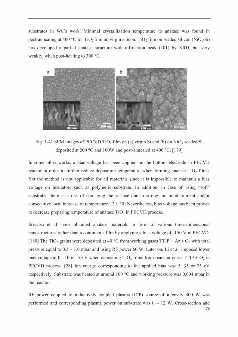
76
substrates in Wu’s work. Minimal crystallization temperature to anatase was found in
post-annealing at 400 °C for TiO2 film on virgin silicon. TiO2 film on seeded silicon (NiOx/Si)
has developed a partial anatase structure with diffraction peak (101) by XRD, but very
weakly, when post-heating to 300 °C.
Fig. 1-41 SEM images of PECVD TiO2 film on (a) virgin Si and (b) on NiOx seeded Si
deposited at 200 °C and 100W and post-annealed at 400 °C. [179]
In some other works, a bias voltage has been applied on the bottom electrode in PECVD
reactor in order to further reduce deposition temperature when forming anatase TiO2 films.
Yet the method is not applicable for all materials since it is impossible to maintain a bias
voltage on insulators such as polymeric substrate. In addition, in case of using “soft”
substrates there is a risk of damaging the surface due to strong ion bombardment and/or
consecutive local increase of temperature. [29, 30] Nevertheless, bias voltage has been proven
to decrease preparing temperature of anatase TiO2 in PECVD process.
Srivatsa et al. have obtained anatase materials in form of various three-dimensional
nanostructures rather than a continuous film by applying a bias voltage of -150 V in PECVD.
[180] The TiO2 grains were deposited at 40 °C from working gases TTIP + Ar + O2 with total
pressure equal to 0.3 – 1.0 mbar and using RF power 60 W. Later on, Li et al. imposed lower
bias voltage at 0, -10 or -50 V when depositing TiO2 films from reactant gases TTIP + O2 in
PECVD process. [28] Ion energy corresponding to the applied bias was 5, 35 or 75 eV
respectively. Substrate was heated at around 100 °C and working pressure was 0.004 mbar in
the reactor.
RF power coupled to inductively coupled plasma (ICP) source of intensity 400 W was
performed and corresponding plasma power on substrate was 0 – 12 W. Cross-section and
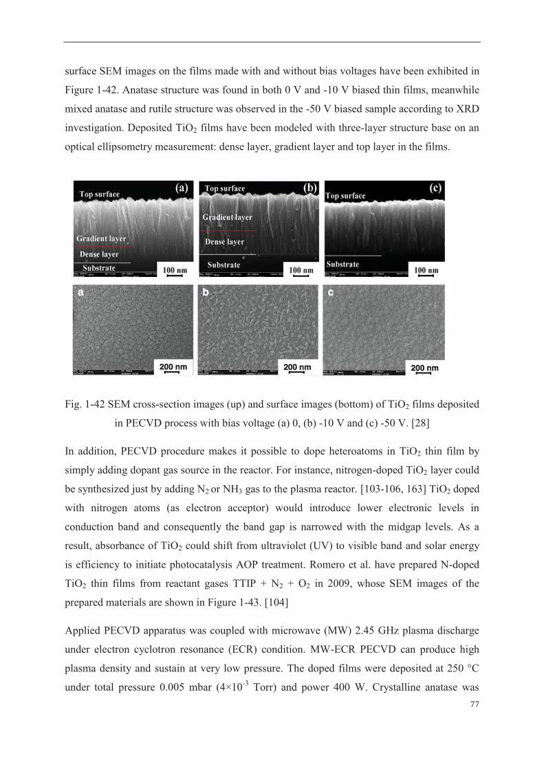
77
surface SEM images on the films made with and without bias voltages have been exhibited in
Figure 1-42. Anatase structure was found in both 0 V and -10 V biased thin films, meanwhile
mixed anatase and rutile structure was observed in the -50 V biased sample according to XRD
investigation. Deposited TiO2 films have been modeled with three-layer structure base on an
optical ellipsometry measurement: dense layer, gradient layer and top layer in the films.
Fig. 1-42 SEM cross-section images (up) and surface images (bottom) of TiO2 films deposited
in PECVD process with bias voltage (a) 0, (b) -10 V and (c) -50 V. [28]
In addition, PECVD procedure makes it possible to dope heteroatoms in TiO2 thin film by
simply adding dopant gas source in the reactor. For instance, nitrogen-doped TiO2 layer could
be synthesized just by adding N2 or NH3 gas to the plasma reactor. [103-106, 163] TiO2 doped
with nitrogen atoms (as electron acceptor) would introduce lower electronic levels in
conduction band and consequently the band gap is narrowed with the midgap levels. As a
result, absorbance of TiO2 could shift from ultraviolet (UV) to visible band and solar energy
is efficiency to initiate photocatalysis AOP treatment. Romero et al. have prepared N-doped
TiO2 thin films from reactant gases TTIP + N2 + O2 in 2009, whose SEM images of the
prepared materials are shown in Figure 1-43. [104]
Applied PECVD apparatus was coupled with microwave (MW) 2.45 GHz plasma discharge
under electron cyclotron resonance (ECR) condition. MW-ECR PECVD can produce high
plasma density and sustain at very low pressure. The doped films were deposited at 250 °C
under total pressure 0.005 mbar (4×10⁻³ Torr) and power 400 W. Crystalline anatase was

78
found in as-deposited films without post-annealing. Varying the nitrogen composition ratio
from 17% to 88%, N-dopant TiO2 films of band gap value 3.14 eV and 2.8 eV were
respectively obtained.
Fig. 1-43 SEM images of N-doped TiO2 films deposited at 250 °C and 400 W in MW-ECR
PECVD with N2 composition ratio (A) 17% and (B) 88%. [104]
Moreover, MW-ECR equipped PECVD set-up has also been carried out to directly deposit
anatase film in some other works by Borras et al. [181-184] and Szymanowski et al. [185]
respectively. According to Borras’ study, it is found that a homogeneous dense TiO2 layer as
“a critical thickness” was formed first and then porous TiO2 layer was deposited on top in
continuous plasma deposition development. They considered that micro-columnar porous
TiO2 layer has lately developed only after the critical thickness was formed. In the same
author’s work, substrate temperatures were experimented from 25 – 250 °C in MW-ECR
PECVD process and 250 °C was determined as optimized parameter regarding to porous
microstructure and morphology of anatase TiO2 films.
Lastly, atmosphere pressure PECVD has also been studied in recent research for depositing
materials including TiO2 films. Since the operation is under ambient conditions, the reactor is
easily simplified and enlarging the capacity is promising to large-surface deposition. However,
more complex composition and much higher pressure in the process may reduce the quality of
films in terms of impurities, stress, morphology and microstructure in comparison to vacuum
plasma deposition. Only very few results on TiO2 materials produced from atmospheric
pressure PECVD (AP-PECVD) have been reported currently. And the photocatalytic
performance of AP-PECVD TiO2 materials can be even rarely studied. An example of

79
atmospheric PECVD TiO2 films deposited at 275 °C with pulse repetition of plasma discharge
(10 and 50 Hz) are presented in Figure 1-44. [186]
Fig. 1-44 SEM image of atmospheric PECVD TiO2 deposited at 275 °C with a pulse
repetition rates (a) 10 Hz and (b) 50 Hz. [186]
2.3 Conclusion
PECVD is an advanced chemical vapor deposition (CVD) technique assisted with electric
power to the reactant gases. A major strength of PECVD process is that the target material
could be deposited at lower substrate temperature in contrast to conventional CVD method. It
could be explained as in the ionized plasma gas phase, thermal/plasma decomposition of the
precursor could occur at lower temperature. Both inorganic (e.g. Si, SixNy and SiO2) and
polymerized films have been obtained with PECVD method reported in recent studies.
According to the literature, silicon- or glass-supported TiO2 films have been deposited either
as amorphous phase or crystalline phase in many PECVD approaches summarized in Tables
1-12 to 1-14 including 1) with/without post-annealing, 2) using RF or MW power discharge,
3) with ICP plasma source, 4) under ECR condition, 5) applying vacuum or room pressures
and 6) using pulsed discharge or not. For as-deposit amorphous TiO2 films, post-annealing
treatment (> 400 °C) has been applied to develop crystallite structure in the films. As-grown
TiO2 film was found in anatase phase deposited at minimal PECVD substrate temperature Ts =
450 °C using RF power 100 W. Otherwise, seeding the substrate prior to PECVD synthesis
has possibly reduced Ts to 300 °C, though the obtained crystalline structure in film was very
inadequate.
80
On the other hand, applying bias voltage during PECVD process has reduced the temperature
of anatase formation to 250 °C, yet continuous TiO2 films were only obtained in some cases
for instance with inductively coupled plasma (ICP) coupled PECVD. In other biased
depositions, TiO2 of three-dimensional nanostructures instead of a layer were obtained.
PECVD using microwave (MW) power of 2.45 GHz in electron cyclotron resonance (ECR)
condition has reduced Ts as low as to 100 °C when forming anatase films. But it should be
noted that MW-ECR PECVD device operates at much higher discharge power (higher than
100 W) in comparison to RF PECVD. Applying a typical RF PECVD approach (without ECR
or pulse repetition), no work has reported preparing temperature of anatase film below 400
°C. Whatever the plasma conditions may be, these are unsuitable for thermal-sensitive
substrates, due to too high substrate temperature, post-heating temperature, discharge power
and/or bias voltage.
The main challenge of this PhD thesis is to deposit anatase thin film using a PECVD process
as a one-step method (or eventually completed with a post-annealing treatment), in operating
conditions suitable for any kind of substrate including polymers. That means that no
bias-voltage and no discharge power higher than 100 W are aimed at. Moreover substrate
and/or post-annealing temperatures should be as low as possible, ideally lower than 250°C,
and if not possible, competitive with regard to temperatures reported in the literature, that is
lower than 400°C.

81
Table 1-12 RF PECVD depositing TiO2 thin films (without post-annealing treatment).
Note: a TTIP: titanium tetraisopropoxide, b silica powder: in PECVD circulating fluidized bed reactor,
c RF 400 W: equipped with an inductively coupled
plasma (ICP) source, d TiO2: in 3D-structured nanoparticles rather than a deposited thin film.
Ref TiO2 thin films Substrate PECVD conditions Crystallization
temp. Working gases Working pressure Substrate temp. Ts Electric power
[187] Amorphous
TiO2 Glass
a TTIP + Ar + O2 TTIP + N2 + O2
0.6 mbar (60 Pa) 120 – 250 °C RF 100 – 500
W -
[25] Anatase TiO2 Silicon TTIP + N2 + O2 0.37 mbar (37 Pa) 450 °C RF 100 W Ts = 450 °C (weakly crystalline)
[188] Anatase TiO2 Glass TTIP + Ar + O2 - 300, 400 °C RF 5 W Ts = 300 °C
[189] Anatase TiO2 b Silica powder
TTIP + He + O2
TTIP + He + Ar + O2 - 250 °C RF 350 W Ts = 250 °C
[8] Anatase TiO2 Glass
Silicon TTIP + O2 0.2 mbar (20 Pa) 40, 300 °C
RF 20 W Bias: -50 V
Ts = 300 °C
[28] Anatase TiO2 Silicon TTIP + O2 0.004 mbar (0.4 Pa) 90 – 140 °C c RF 400 W Bias: -50 V
Ts ~ 100 °C
[180] d TiO2 Si TTIP + Ar + O2 0.5 mbar (50 Pa) Room temp. (25
°C) RF 60 W
Bias: -150 V Ts = 25 °C
[190] Anatase TiO2 Silicon TCl4 + O2
TCl4 + Ar + O2 0.13 mbar (13.33
Pa) 135 °C
Pulsed RF 200 W
Ts = 135 °C
[186] Anatase TiO2 Glass TCl4 + O2 Atmosphere (1 bar) 275 °C Pulse
(50 kHz) Ts = 275 °C

82
Table 1-13 MR-ECR PECVD depositing TiO2 thin films without post-annealing treatment.
Note: 8MW-ECR: microwave electron cyclotron resonance with 2.45 G.
Ref TiO2 thin films Substrate PECVD conditions
Crystallization temp.
Working gases Working pressure Substrate temp. Ts Electric power
[183] Anatase TiO2 Silicon TTIP + Ar + O2 0.005 mbar
(4×10⁻³ Torr) 250 °C
a MW-ECR
400 W Ts = 250 °C
[104] Anatase TiO2 Silicon Quartz
TTIP + N2 + O2 0.005 mbar
(4×10⁻³ Torr) 250 °C
MW-ECR
400 W Ts = 250 °C
[185] TiO2 Glass TCl4 + O2
0.005 mbar
(4×10⁻³ Torr) 250 °C
MW-ECR
400 W Ts = 250 °C
[191] Anatase TiO2 Silicon TTIP + N2+ O2 - - MW-ECR -

83
Table 1-14 PECVD as-deposit TiO2 thin films with post-annealing treatment.
Ref TiO2 thin films Substrate
PECVD conditions Post-annealing
Tp Crystallization
temp. Working gases
Working pressure
Substrate temp. Ts
Electric power
[192] Anatase/rutile
TiO2 Silicon TTIP + Ar + O2 - 200 °C RF 60 W 400 °C Tp = 400 °C
[193] Anatase TiO2 Silicon a TE + O2 - 350 °C RF 300 W 500 °C Tp = 500 °C
[178] Anatase TiO2 Silicon TTIP + Ar + O2 1.33 mbar
(133 Pa) 350 °C RF 100 W 600, 900 °C
Tp = 600 °C (very weakly
crystallized at 350 °C)
[26] TiOx:OH - TTIP + O2 - 200 °C - 300 – 700 °C Tp = 400 °C
[179] TiOx:OH Silicon
b NiOX/Si Quartz
TTIP + N2 + O2 0.4 mbar (40 Pa)
200 °C RF 100 W 300 – 600 °C Tp = 400 °C
Note: a TE: titanium (IV) ethoxide and b NiOx/Si: NiOx-seeded (20 nm thick) silicon made from e-beam evaporation and oxidation process.

84

85
Chapter II Experimental details
This chapter presents the operating conditions for the preparation and characterization of TiO2
thin films. It is divided into three parts. The first part is dedicated to the preparation of
materials including PECVD deposition, post-annealing and seeding approach. The second and
third parts are related to implemented methods for the characterization of films in terms of
physico-chemical (part 2) and functional (part 3) properties.
1 Preparation of supported TiO2 thin films
In a first step, PECVD operating conditions have been experimented and optimized in order
to deposit TiO2 coating on different mechanical supports including dense and porous ones. As
no anatase structure could be obtained for deposition temperature lower than 250°C, a
post-thermal treatment has been envisaged and optimized in terms of temperature and time
required for crystallization. In parallel, seeding the substrate with crystal nuclei before
deposition has been investigated with the aim of getting anatase directly through the PECVD
deposition step.
1.1 Deposition of films by PECVD method
1.1.1 PECVD set-up
The PECVD system used in this study was typically composed of four main parts: the
precursor and gases sources, the reaction chamber (i.e. the deposition chamber), the power
generator and the pumping system, as notified on the photo and schematic graph of PECVD
apparatus (excluding the pumping system) in Figure 2-1 and Figure 2-2, respectively. Each
constitutive part of the PECVD system is detailed below.

86
Fig. 2-1 Photo of the PECVD apparatus.
Fig. 2-2 Schematic graph of the PECVD apparatus.

87
Precursor and gases sources
The liquid metal-organic precursor contained in a sealed glass was held in an oil bath heated
at 80 °C and stirred with Magnetic Stirrers from KA®, WERKE GmbH & Co. KG
(Germany). Fluxes of argon and oxygen were regulated with a mass control unit of
ROD-4MB, HORIBA (Japan). The inert argon (argon) was bubbling in liquid precursor as a
carrier gas. The gas line connecting precursor source and reaction chamber was wrapped with
circular coil of 220V Desostat-1D, L.LEGALLAIS (France) so that the line could be heated at
100 °C to avoid any precursor condensation in the pipe. Indeed, condensation causes pipe
blockage, which can destabilize vacuum condition and produce TiO2 powder falling down on
the substrate. A thermal couple of Series 988, WATLOW (USA) was inserted between the
coil and the pipe monitoring the actual temperature on the gas line. Oxygen was introduced as
oxidant gas through an individual pipe directly connected to side of the reaction chamber.
Reaction chamber
The reaction chamber was a 10 liters steel cylinder equipped with a pressure gauge and two
horizontal parallel plate electrodes. The pressure gauge (600 series/Baratron®, MKS
Instruments GmbH (Germany)) was employed to investigate the pressure inside reaction
chamber in real-time. The bottom electrode (diameter 10 cm) was used as the substrate
holder. It was connected to a heating device from Eurotherm (France) heating up to 600°C.
Bottom electrode (diameter 10 cm) and body of the chamber were grounded. The upper
electrode (diameter 10 cm) was coupled to the power generator via metallic wires. One hole
has been drilled in the center of the upper electrode, as a showerhead form, in which the
carrier gas and precursor were injecting.
Power generator
R.F. power generator (CESARTM 136, Advanced Energy Industries Inc., USA) coupled with a
matching box (RF navio, Advanced Energy Industries Inc., USA) was connected to the upper
electrode on top of the chamber. A Teflon tube was needed to electrically separate the
powered upper electrode from the grounded chamber.

88
Pumping system
The bottom of the reaction chamber was connected to a pumping system composed of a cold
trap and a primary pump (Adixen, Pfeiffer Vacuum GmbH (Germany)). The cold trap
placed between the deposition chamber and the pump enabled to retain the non-reactive
species during the deposition process. The primary pump had two different roles: exhausting
atmospheric gases and vapors (down to around 1 Pa) before the deposition step, and
maintaining the required plasma pressure during the deposition process.
1.1.2 Precursor and substrates
Titanium tetra-isopropoxide (TTIP, Ti(OCH(CH3)2)4) from Sigma-Aldrich (Germany) has
been chosen as the metal-organic precursor to synthesize TiO2. Chemical structure of TTIP
molecule is given in Figure 2-3. TTIP is an effective precursor and less toxic than titanium
chloride (TiCl4), which is another common precursor for producing TiO2. Hydrolysis of TTIP
is easily taking place when it is in contact with water or air humidity. Therefore, filling TTIP
liquid to the precursor tank and sealing the container was operated in a vacuum glove box
workstation. The glove box was controlled at pressure of 1 mbar with water concentration <
1.2 ppm and oxygen concentration < 1 ppm. Afterwards, the sealed container was connected
to the plasma reactor and kept in oil thermal bath.
Fig. 2-3 Chemical structure of TTIP precursor.
In the literature, thermal decomposition of TTIP molecule has been analyzed in a CVD
chamber coupled with mass spectrometry detection. [175] Propene (gas phase), water (gas
phase) and titanium dioxide (solid phase) were found as the three main products from the
reaction. Isopropanol was also observed as intermediate from hydrolysis and
self-fragmentation of TTIP compound as written in Reaction 2-1 and Reaction 2-2.
Isopropanol is further dissociated to water and propene as given in Reaction 2-3. Eventually,

89
generalized reaction of TTIP breaking down to TiO2, H2O and C3H6 is summarized in
Reaction 2-4.
Hydrolysis of TTIP:
Ti (OCH (CH3)2)4 (g) + 2 H
2O (g) → TiO
2 (s) + 4 (CH
3)2CHOH (g) (2-1)
Break-down of TTIP:
Ti (OCH (CH3)2)4 (g) → TiO
2 (s) + 2 C
3H
6 (g) + 2 (CH
3)2CHOH (g) (2-2)
Isopropanol to propene:
(CH3)2CHOH (g) → H
2O (g) + C
3H
6 (g) (2-3)
Overall reaction:
Ti (OCH (CH3)2)4 (g) → TiO
2 (s) + 2 H
2O (g) + 4 C
3H
6 (g) (2-4)
In a PECVD process, electron collision to molecules and ion-molecule interactions are also
important. Yet no specific study has been reported on TTIP decomposing pathways (possibly
of subsidiary interaction/reaction) in PECVD process.
Mechanical support was mounted on the bottom electrode for plasma deposition. Dense
substrates such as silicon wafer and glass slide were applied to support TiO2 thin film for
characterization purpose. Silicon-supported TiO2 layers were characterized for their chemical
composition, morphology, wettability and crystalline structure and glass-supported TiO2
layers were studied for band gap energy. Self-cleaning property of TiO2 deposited on silicon
were investigated following the Pilkington protocol. On the other hand, porous substrates
such as ceramic and glass were used to fabricate functionalized membranes after optimized
PECVD conditions have been established from the characterization stage. The applied dense
and porous substrates are listed in Table 2-1.
Porous Anodisc (from Sigma-Aldrich) and porous ceramic disks (from Fraunhofer) are in
round shape with a diameter of 47 mm. Anodisc is 0.1 mm thick and has a mean pore size
equal to 250 nm. Ceramic disks are 1 mm thick with an asymmetric porous structure (Figure
2-4). They are composed of a macroporous support with a mean pore size of 2.5 µm and of a
top layer with a smaller mean pore size. Two types of ceramic disks, characterized by top
layers with two different mean pore sizes, 100 nm (Figure 2-4) and 800 nm, were used. The
choice of two different ceramic supports is directly related to the wish to get two different
geometries of titania materials. Indeed, two different kinds of TiO2 coatings were deposited

90
on them as: a continuous micrometer thick layer on 100 nm pored surface and a nanometer
thick thin skin-coverage on 800 nm pored surface.
Table 2-1 Applied substrates to support TiO2 thin films in PECVD process.
Dense substrate Porous substrate
Si (100) wafer,
MEMC (Korea)
Whatman® Anodisc 47,
Sigma-Aldrich (Germany)
Borosilicate glass,
Pyrex (France)
Ceramic Al2O3 disk,
Fraunhofer (Germany)
Quartz glass Mat of borosilicate glass fibers,
Hollingsworth & Vose (USA)
A mat of borosilicate glass fibers (from H&V, USA) is another porous substrate that needs to
be cut into a circle with 47 mm diameter to fit into the membrane cell. Thickness of the
fiberglass mat is 0.4 mm and means pore size is 2.7 µm. Information about the porous
substrates are summarized in the Table 2-2. Anodisc 47 support was used in preliminary
synthesis to check TiO2 morphology grown on porous surface. Ceramic Al2O3 disk and glass
fiber were coated with TiO2 materials and then tested in photodegradation diffusion cell and
pilot plants.
Fig. 2-4 Asymmetric porous alumina ceramic disk (from Fraunhofer) used as the support for
PECVD TiO2 thin film.

91
Table 2-2 Physical properties of the porous substrates.
Porous substrate Mean pore size Thickness Diameter
Whatman® Anodisc 250 nm 0.1 mm 47 mm
Ceramic Al2O3 disk Top-layer 100 nm
Top-layer 800 nm
1 mm 47 mm
Mat of borosilicate glass fibers 2.7 µm 0.4 mm -
Substrate surface was cleaned with ethanol and dried with air blowing before being mounted
in the reactor. It was placed in the center on the bottom electrode just under the precursor inlet
hole. Thermal-stable tape was used to fix the substrate on the edge.
1.1.3 Plasma deposition protocol and operating conditions
The plasma deposition protocol is presented in Table 2-3. Once the substrate fixed on the
bottom electrode, all temperatures (oil bath, lines, substrate holder) and limit pressure in the
reactor achieved, precursor and gases were introduced in the reaction chamber. Once the
precursor and gases pressures stabilized, the RF power generator was switched on at the
required power for the suitable duration depending on the targeted deposition thickness.
Table 2-3 Plasma deposition protocol.
1 Fill the precursor
§ Pour TTIP liquid in to container in Gloves Workstation § Seal the container well § Connect the precursor container to the reactor 2 Prepare the reactor
§ Wrap the bottom electrode with aluminum paper § Fix the substrate in the center of bottom electrode § Connect the upper electrode, Teflon tube and the reactor § Measure the distances from the top to the upper and bottom electrodes § Close the reactor and start pumping to vacuum condition
92
3 Start heating
§ Heat the oil bath (precursor) to 80 °C § Heat the gas carrier line to 100 °C § Heat the substrate holder to target temperature § Cool the trap with liquid nitrogen 4 Introduce gases
§ Open valves and inject argon and precursor vapor to the reactor § Open valves and inject oxygen to the reactor 5 Plasma on
§ Switch on RF power generator § Select ‘‘real mode’’ and input the intensity value § Increase the tune capacity (CT) to 99.5 % § Reduce the load capacity (CL) to 8.5 % § Push the ‘‘on’’ button to initialize the plasma and start depositing § Refill liquid nitrogen to cool the trap each 5 min § Push the “off” button to stop the plasma 6 End the process
§ Stop argon and oxygen gases § Stop pumping and wait till minimal pressure § Stop heating § Open the reactor and collect TiO2 sample § Clean the reactor and trap
As RF power is on, gaseous molecules would be excited, ionized, dissociated and fragmented.
Species such as hot electrons, radicals, ions and neutrals are typically formed in the plasma.
Some transition of the electrons results in photon emission and thus the plasma is normally
brightly illuminating. A photo of the PECVD reactor chamber obtained during a deposition
process is displayed in Figure 2-5. The whitely plasma can be observed through the window
glass.
A few points on an appropriate PECVD operation have to be declared. For instance, heating
the gas lines constantly before gases inlet and until all the gases are stopped is very important
to keep the pipes clean from condensation. The order of opening and closing gas valves (for
argon and oxygen) should be correctly followed so that the liquid precursor would not be in
contact to vacuum or oxygen directly. In addition, when applying the real mode on power
generator, capacitances have to be adjusted in order to reduce the reflected intensity.

93
Fig. 2-5 Photo of the working PECVD reactor chamber.
PECVD operating conditions include: 1) thermal factors such as temperatures of substrate,
precursor and gas line, 2) pressure factors such as partial pressure of Ar + TTIP and of O2, 3)
real electric power, 4) reactor configuration and 5) deposition duration. Detailed PECVD
parameters for TiO2 deposition are given in Table 2-4. Certain operating factors have been
varied in order to study their effect on TiO2 film growth on silicon.
Table 2-4 Controlled PECVD parameters in TiO2 preparation.
Temperatures Pressure RF power Plasma
dimension
Deposition
duration
Substrate temp.
Ts = 50 – 250°C
Vacuum pressure
P0 = 0.01 mbar (1 Pa)
Real power
Wreal = 50 – 65
W
Electrode diameter
De = 10 cm
t = 3 – 40
min
Precursor temp.
Toil = 80°C
Argon + TTIP pressure
PAr + TTIP = 0.155, 0.185,
0.225 mbar
Plasma distance
dP = 2.0, 2.5,
3.0 cm
Gas line temp.
Tline = 100°C
Oxygen pressure
PO2 = 0.17 mbar
Substrate temperature (Ts) is important for surface reaction and surface diffusion/migration
kinetics. It was varying from 50 to 250 °C in the studied PECVD process. Temperature of the
94
oil bath (Toil), that is the precursor temperature, was kept at 80 °C and temperature of the gas
line (Tline) was maintained at 100 °C in the process.
The gas partial pressures were used instead of gas flow rates because millimeter valves were
used in the gas line instead of flow meters to control the input gas flows. Partial pressure of
Ar + TTIP (PAr+TTIP) and partial pressure of O2 (PO2) were calculated according to Equation
2-5 and 2-6 with knowing P0 (initial limit pressure in the deposition chamber), P1 (argon +
TTIP partial pressure) and P2 (total pressure once oxygen introduced). The influence of both
PO2 (varying from 0.15 to 0.19 mbar) and PAr+TTIP (equal to 0.155, 0.185 or 0.225 mbar) on
the deposit chemistry and thickness homogeneity was studied.
Partial pressure of argon and precursor (Ar + TTIP):
PAr + TTIP = P1 – P0 (2-5)
Partial pressure of oxygen:
PO2 = P2 – P1 (2-6)
where P0 is the initial limit pressure in the deposition chamber, P1 is the pressure on
ce argon and TTIP introduced and P2 is the pressure after addition of oxygen.
RF power is the energy source to produce the weakly ionized plasma in PECVD process so
that TiO2 solid nanoparticle is eventually deposited on a surface. Forward electric power was
supplied from the generator, whereas the reactor reflected some and only part of the power
was enforced to the reactor. Then the real power can be known as written in Equation 2-7.
Two different real powers equal to 50 W and 65 W were applied in this study.
Real power intensity:
Wreal = Wf – Wr (2-7)
where Wreal is the real power on upper electrode, Wf is the forward power supplied by
generator and Wr is the reflected power from the chamber.
Reactor configuration, the space between two electrodes in particular, affects the geometry of
the plasma phase and consequently the properties of the deposited films. Diameter of both

95
electrodes (De) was 10 cm and the distance between them (dp) was 2 – 3 cm adjusted by
replacing a Teflon joint tube of different length. The distance from the reactor top to the
bottom electrode (d2) and the distance from the top to upper electrode (d1) were measured. As
a result, the plasma pathway length (i.e. electrode distance) was obtained by the first distance
minus the second one as given in Equation 2-8. The influence of the plasma distance (equal to
2.0, 2.5 or 3.0 cm) on deposits chemistry and thickness homogeneity was studied.
Plasma distance:
dp = d2 – d1 (2-8)
where dp is the length of plasma pathway, d1 is the distance from the chamber top to upper
electrode and d2 is the distance from chamber top to bottom electrode.
Three different deposition durations were applied: 15, 20 and 40 min in the case of
TiO2-coating layer on silicon, quartz and porous ceramic substrates. On the other hand, four
different deposition durations equal to 3, 5, 7 and 10 min was experimented on porous
ceramic support (with 800 nm mean pore size) for TiO2-skin coverage coating.
As a summary, all the TiO2 samples prepared in this thesis work are presented in Table 2-5
listing the substrate material, substrate temperature, plasma conditions and deposition
duration. Groups of sample B 1-5, ZJ 1-9 and M 1-4 (on silicon) were dedicated for PECVD
optimization studies. Samples Q 1-3 were made on transparent quartz for light transportation
study. Samples sS 1-2 were made on seeded silicon for crystallization process during
post-annealing treatment. Samples M100, M800, LF100 and LF800 were PECVD prepared
TiO2-ceramic composite membranes having different formates of TiO2 coating on the porous
ceramic support.

96
Table 2-5 List of all the TiO2 thin films prepared in this Ph.D work.
Plasma deposition is a dynamic process in which the working pressures and electric powers
are fluctuating along with deposition time. Reactor pressure and discharged power were
recorded every minute when preparing TiO2 thin films. Recorded values in the case of a TiO2
film deposited in optimized synthesis conditions (determined from films properties – see
chapter 3) are given in Table 2-6. It is observed that reaction pressure surged up in the first a
few seconds the plasma was just initiated and followed with a fast dropping. After about 2
minutes, working pressure slowly climbed up due to collision and reaction in the gas phase.
TiO2 sample Substrate
Substrate
temperature
(°C)
Ar+TTIP
pressure
(mbar)
Plasma
distance
(cm)
RF
power
(W)
Deposi-
-tion
duration
(min)
B 1-5 Silicon
50 100 150 200 250
0.15 3 60 15
ZJ 1-9 Silicon 150 0.155, 0.185, 0.225
2 2.5 3
50 20
M 1-4 Silicon 150 0.225 2 3
50 65
20
Q1-3 Quartz 150 0.225 3 50 7
15 20
sS 1-2 Seeded silicon
150 250
0.225 3 50 50
M100 Porous ceramic
(Pr=100nm) 150 0.225 3 50 20
M800 Porous ceramic
(Pr=800nm) 150 0.225 3 50 7
LF100 Porous ceramic
(Pr=100nm) 150 0.225 2 50
20 40
LF800 Porous ceramic
(Pr=800nm) 150 0.225 2 50
20 40

97
Eventually, the total pressure stabilized roughly in the last a few minutes. As deposition going
on, real power to the reactor was always fixed and forward power continuously increased
since reflection from the chamber was keeping enhanced. The increased reflect power can be
explained by more solid materials was attached to the upper electrode during deposition
process. Constant real power intensity with a lower forwarding power is desired because
carbonization of the precursor compound could be weakened.
Table 2-6 Dynamic reaction pressure and electric power in an optimal PECVD process.
1.2 Crystallization by post-annealing
As-grown TiO2 films obtained from the mentioned PECVD protocol was obtained in
amorphous phase. Since crystalline TiO2 (anatase phase) is the most photocatalytic efficient
form, great efforts were made to find temperature threshold in TiO2 phase transformation
from amorphous to anatase. Post-annealing the deposited films was operated in the furnace of
VULCAN® 3-130, DETSPLY International (USA). Heating temperature, heating/cooling
speed and dwelling time (i.e. staying duration) were programed on the furnace. Heating rate
1.0 °C min-1 and cooling rate 10 °C min-1 was applied in the most post-thermal treatments,
whereas, slower heating speed 0.5 °C min-1 was experimented to investigate potential effect
Duration
(min)
Reaction
pressure (mbar)
Forward
power (W)
Reflected
power (W)
Real power
(W)
0.1 0.590 130 80 50
2 0.490 96 46 50
4 0.483 112 62 50
6 0.490 120 70 50
8 0.495 130 80 50
10 0.506 134 84 50
12 0.520 138 88 50
14 0.524 139 89 50
16 0.516 140 90 50
18 0.516 145 95 50
20 0.516 147 97 50

98
on crystallization. Post-annealing process was studied in two situations: 1) as a function of
increased temperatures from 300 to 700 °C and 2) as a function of dwelling time at fixed 300
°C.
1.2.1 Post-annealing as a function of temperature 300 – 700 °C
First of all, TiO2 thin film grown on silicon was synthesized with the optimized PECVD
protocol. The sample was mounted in a high-temperature X-ray diffraction apparatus (X'pert
Pro, Pan Analytical) that contained a compacted furnace. Silicon-supported TiO2 thin film
was heated from 100 to 700 °C with a heating rate 1 °C min-1; at the meantime, X-ray
diffraction measurement was taking place at each 100 °C increased temperature. The minimal
temperature of crystallization was found in the continuous heating manner. Detail on
diffraction measurement is to be explained in a following session 2.2.3 in this chapter.
In addition, four other samples of TiO2 thin films on silicon were prepared under the
optimized PECVD conditions. One sample was kept as deposited, the other three were heated
to 300, 400 and 500 °C respectively in the furnace. Heating and cooling steps were kept in
rates of 1.0 and 10 °C min-1. No staying duration was applied to all the samples after reaching
the target temperature. The heating programs are given in the Figure 2-6.
Fig. 2-6 Post-heating TiO2 samples at Tp equal to 300, 400 or 500 °C.
Afterwards, room temperature XRD analysis was carried on the post-annealed TiO2 samples
to examine whether crystalline structure has been formed. In addition, a slower heating rate
0.5 °C min-1 was applied on heating a fifth sample at 300 °C with other conditions constant in
order to investigate the possibility of crystallization at 300 °C without staying time.
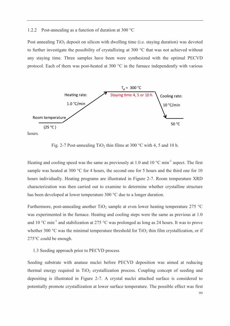
99
1.2.2 Post-annealing as a function of duration at 300 °C
Post annealing TiO2 deposit on silicon with dwelling time (i.e. staying duration) was devoted
to further investigate the possibility of crystallizing at 300 °C that was not achieved without
any staying time. Three samples have been were synthesized with the optimal PECVD
protocol. Each of them was post-heated at 300 °C in the furnace independently with various
hours.
Fig. 2-7 Post-annealing TiO2 thin films at 300 °C with 4, 5 and 10 h.
Heating and cooling speed was the same as previously at 1.0 and 10 °C min-1 aspect. The first
sample was heated at 300 °C for 4 hours, the second one for 5 hours and the third one for 10
hours individually. Heating programs are illustrated in Figure 2-7. Room temperature XRD
characterization was then carried out to examine to determine whether crystalline structure
has been developed at lower temperature 300 °C due to a longer duration.
Furthermore, post-annealing another TiO2 sample at even lower heating temperature 275 °C
was experimented in the furnace. Heating and cooling steps were the same as previous at 1.0
and 10 °C min-1 and stabilization at 275 °C was prolonged as long as 24 hours. It was to prove
whether 300 °C was the minimal temperature threshold for TiO2 thin film crystallization, or if
275°C could be enough.
1.3 Seeding approach prior to PECVD process
Seeding substrate with anatase nuclei before PECVD deposition was aimed at reducing
thermal energy required in TiO2 crystallization process. Coupling concept of seeding and
depositing is illustrated in Figure 2-7. A crystal nuclei attached surface is considered to
potentially promote crystallization at lower surface temperature. The possible effect was first

100
examined during plasma deposition process with substrate temperature at 150 °C and 250 °C.
The effect on crystallization was secondly examined during post-annealing process at 300 °C.
Fig. 2-8 Concept of using seeded substrate for PECVD TiO2 deposition.
1.3.1 Seeding the substrate by sol dip-coating
The anatase sol for seeding substrate was basic hydrosol S5-300B provided by Millennium
Inorganic Chemicals (France). Anatase solution was prepared by diluting the original sol in
ammonia buffer at pH 11.5 with a ratio 1:7.5. After sufficient mixing for 4 hours, a piece of
virgin silicon was vertically dipped into the solution with a homemade mechanical device.
Sinking speed 5 cm min-1 and immersion time 20 seconds were set constantly. Withdrawing
velocity was experimented with 1, 3 and 5 cm min-1 respectively to attach a seeding layer of
proper thickness and dispersion on silicon. After one step of dipping, the wetted silicon pieces
were vertically dried in air for one night. And then they were heated at 250 °C for 24 hours
and then at 450 °C for another 24 hours in the furnace to remove organic solvent. Heating rate
and cooling rate were 5 and 10 °C min-1 respectively. The preparation routine was adapted
from a previous work of depositing anatase on porous ceramic using sol-gel method published
by A. Ayral.[14]
Surface hydrophilicity is essential to provide a homogeneous dispersion of sol on silicon with
dip-coating approach. 800 °C-annealed silicon was prepared in the furnace so that an oxidized
surface was maintained in order to improve its surface wettability in comparison to the virgin
silicon (100) wafer. Seeding approach was carried out on the annealed silicon substrate with
the same dip-coating process described as previously.
Homogeneity of crystal nuclei dispersion on silicon surface is the key point to obtain a fully
seeded-substrate that is to be mounted in PECVD reactor. Adhered anatase on both virgin and
annealed silicon was witnessed with confocal Raman spectroscope. The seeded surface was
101
also observed in the coupled microscope. Moreover, the seeding layers were observed in
cross-sectional SEM images.
1.3.2 PECVD TiO2 deposition on the seeded substrate
The best seeded-silicon and virgin silicon (as witness substrate) were fixed on the bottom
electrode in PECVD reactor. TiO2 thin films were deposited upon them under optimal plasma
deposition conditions. In the case of seeded-substrate, two deposition experiments were
particularly studied with substrate temperature at both 150 °C and 250 °C. It is more likely
that TiO2 deposit might be crystallized due to stronger seeding activity at higher surface
temperature. A substrate temperature higher than 300 °C was not intended in the thesis work
by applying PECVD process because post-thermal treatment would be carried out equal to or
above 300 °C after all.
As-deposit TiO2 thin films on seeded and non-seeded silicon (both prepared at 150 and 250
°C) were examined with XRD and Raman spectroscope right after PECVD process.
Afterwards, the four samples went through the analysis in high-temperature XRD heating at
300 °C. Measurement duration at 300 °C lasted for 6 hours on each sample. Diffraction
pattern was recorded each other half an hour at 300 °C. Phase transformation from amorphous
TiO2 to anatase was traced as function of heating duration and compared on the effect of
seeding surface and deposited temperature.
2 Characterization on physico-chemical properties of TiO2 films
Physico-chemical properties of TiO2 thin films investigated in this study are morphology,
surface wettability, chemical composition, crystalline structure, porosity, density and band
gap energy. Fourier transformed infrared spectroscope (FTIR) and energy dispersion X-ray
(EDX) were employed to analyze chemical bonding and elemental composition in the films.
Scanning electron microscope (SEM) imaged the microstructure in the films. Water contact
angle (WCA) examined TiO2 surface hydrophilicity with or without the effect of UV
irradiation. X-ray diffraction (XRD) and Raman spectroscope were applied to investigate the
crystal structure in annealed films. X-ray reflectivity (XRR) and ellipsometry spectroscope
(EP) were experimented and modeled to calculate film porosity. Optical absorbance measured
in UV/Vis spectroscopy was plotted to determine the band gap energy of synthetic TiO2 film
102
on glass. Moreover, thermal analysis on heat transfer and weight loss was carried out for
prepared TiO2 materials by heating in the range 25 – 1000 °C.
2.1 Morphology, Chemistry, surface wettability and crystal structure (SEM, FTIR, EDX,
WCA, XRD and Raman)
Morphology
Morphology of TiO2 layer (amorphous and anatase) on silicon was inspected in scanning
electron microscope (SEM), Hitachi S4800 (Japan). Samples were cut into suitable size and
then horizontally and vertically mounted on SEM substrate holder for surface and
cross-sectional scanning. The cut edge for cross-sectional purpose should be sharp and fresh.
Each sample was metallized with Pt plasma pre-treatment for 40 seconds before inputting to
the SEM sample chamber. Electron beam of energy 10-100 kV was shooting on the sample so
that proportional magnified images were produced. Microstructure of the thin film was
observed in surface and cross-section images. Thickness of TiO2 layer was measured in SEM
cross-sectional image, which was bearing 10% instrumental error. Furthermore,
microstructure of as-deposit and annealed TiO2 film (for the same sample) was compared in
SEM images to check whether the post-annealing caused structure change or defect.
Chemistry
PECVD TiO2 deposit on silicon was analyzed with FTIR, 710 Nicolet (France), as well as the
corresponding post-annealed ones. The infrared absorbance spectrum of silicon-supported
TiO2 thin film was recorded in the wavenumbers range 400 – 4000 cm-1, with an automatic
subtract of silicon background in the Omnic program. Vibration due to O-H bond of adsorbed
surface water, organic bond C-C and inorganic bond Ti-O was observed in infrared spectra.
Normalized absorbance intensity of Ti-O vibration at wavenumber 450 cm-1 was calculated
by dividing the measured intensity (from FTIR spectrum) with the film thickness. By
comparing normalized intensity (independent of thickness) of samples made from different
PECVD conditions, the sample with the richest Ti-O abundance was found and accordingly
the optimal deposition parameters were determined. Infrared spectra of amorphous and
anatase film (from the same sample) were recorded and difference was observed. In addition,
chemical elements in the as-deposit film were analyzed in energy dispersion X-ray (EDX),

103
Hitachi S4800 (Japan) from 0 – 10 keV. Elements and relevant atom ratio were estimated
from EDX spectrum.
Surface wettability
Homemade water contact angle (WCA) device coupled with CCD detector was employed to
study surface wettability of TiO2 film with or without effect of UV illumination. Surface of
both amorphous and anatase films on silicon was studied. In darkness, a droplet of pure water
(from Millipore) with volume 0.6 ml was dropping from a syringe onto the film and
immediately a photo of the TiO2-water interface was captured by detector camera. Five
positions on the surface were analyzed and thus an average contact angle was obtained for
each sample. The photos were analyzed in a graphic program to measure and fit the
solid-liquid contact angles. Afterward, the same sample was placed under a UV lamp of
intensity 30 W m-2 at wavelength 355 nm for 20 minutes. The same WCA measurement as
previous was made on the illuminated TiO2 surface immediately after UV treatment. Mean
water contact angle on irradiated and non-irradiated TiO2 surface (for the same sample) was
compared and the photo-induced hydrophilicity phenomenon was investigated. Difference of
wettability between amorphous and crystalline surface was also compared.
Crystalline structure and crystallite size
Crystalline phase of post-annealed TiO2 film was examined with X-ray diffraction (XRD) of
X'pert Pro, Pan Analytical (Netherland) by matching the measured pattern to the database.
Effect of PECVD substrate temperature and post-annealing temperature on crystal formation
in the films was evaluated in the patterns. TiO2 layer deposited on seeded-silicon was also
studied in diffraction analysis. Incident X-ray was emitted from Cu Kα at wavelength 0.154
nm. XRD operational power was 40 kV and 20 mA and measuring angle 2θ was from 20 – 60
° with a rotating speed 0.028 ° s-1. In a result, one XRD recording on one TiO2 sample took 25
minutes.
Crystallite size was estimated according to Scherrer equation as given in Equation 2-9, with
knowing peak width in XRD pattern. For instance, by measuring the full-width at half
maximum ∆(2θ)FWHM at 2θ = 25.3 , crystal dimension D in the anatase TiO2 film can be know
from the below equation.

104
Scherrer equation:
s = # uvw#6x#yz{K######## (2-9)
where 0.9 is a constant (for sphere shape crystal), 6 is the wavelength of incident X-r
ay (0.154 nm), θ is the incident angle and B is the radius value related to∆(2θ)FWHM
and instrumental resolution.
The radius value B as:
x = #|BM}KO~���k . BM}KO@QLk ###### (2-10)
where ∆(2θ)FWHM is full-width at half maximum at 2θ in diffraction pattern and ∆(2θ)
res is instrumental resolution (equal to 0.09 for the applied XRD apparatus).
In addition, Raman spectroscope (from Jobin-Yvon Confocal Labram 1B) provided
complementary characteristic spectrum on crystal structure. The confocal Raman
spectroscope was coupled with Olympus BX40 microscope. TiO2 anatase has fingerprint
Raman scattering with incident light. Red laser of intensity 100 mW at wavelength 647.1 nm
was emitted from Ar/Kr to stimulate molecular vibration in the sample. A detection network
1800 lines nm-1 for scattered light was chosen in a measuring window 150 – 800 cm-1. Sensor
CCD 30-11 (1024 × 256 pixels) was coupled to the Raman spectroscope for imaging on
sample surface with a magnified lens ×100 times. As-grown and annealed TiO2 films on
silicon were examined in Raman spectroscope to confirm the anatase structure. Moreover,
seeding layer on silicon and TiO2 on seeded-silicon (as described in session 1.3 in this
chapter) were also investigated with vibrational spectroscope. It is more feasible to analyze
very thin anatase layer with confocal Raman spectroscope than with XRD.
2.2 Porosity and band gap energy (XRR, EP and UV/Vis)
Porosity
Porosity in the TiO2 film on silicon was not directly measured with nitrogen
adsorption/desorption method due to the limitation of material quantity inherent to thin film.
Density of the film was modeled from X-ray reflectivity (XRR) fitting using X-ray
diffractometer D5000, Siemens (Germany). The density of synthetic TiO2 film was compared

105
to the density of dense TiO2 material and therefore the percentage of void volume was
calculated as given in the Equation 2-11.
Porosity of thin film:
� = N��N.N��}N��N × Nuu� (2-11)
where ρ1 is the density of PECVD TiO2 film and ρ2 is the density of dense TiO2 as a
reference.
Porosity, thickness and refractive index of the thin film could also be modeled in optical
ellipsometry spectroscope (EP) and XRR measurement with the methods described in one
previous work of the group [194]. Light of energy in the range 1.2 – 4.5 eV was incident on
TiO2 surface with a spot area 3 cm2. Polarization of the reflected electromagnetic wave was
detected and calculated. A few mathematics laws were applied and modified to fit the
measured data in the program. An example of Cauchy law is given in Equation 2-12.
\#M6O = x : P6} (2-12)
where n is refractive index, λ is the wavelength, B and C are the equation coefficients.
Band gap energy
Band gap energy (Eg) of semiconductor has been explained in the first chapter. The band gap
of PECVD TiO2 thin film on glass was studied with optical measurement. Borosilicate glass
(Pryex) and quartz were applied as the transparent substrates. Optimal PECVD conditions
were operated to prepare TiO2 films on glass with deposition duration as 7, 15 and 20 minutes
so that various thicknesses were obtained. Post-annealing at 400 °C was carried out in the
furnace to produce anatase phase. Amorphous and anatase films on glass were analyzed with
UV/Vis spectroscope V-570, JASCO from Serlabo Technologies (France). Absorbance,
transmittance and reflectance data were collected from wavelength 200 to 700 nm.
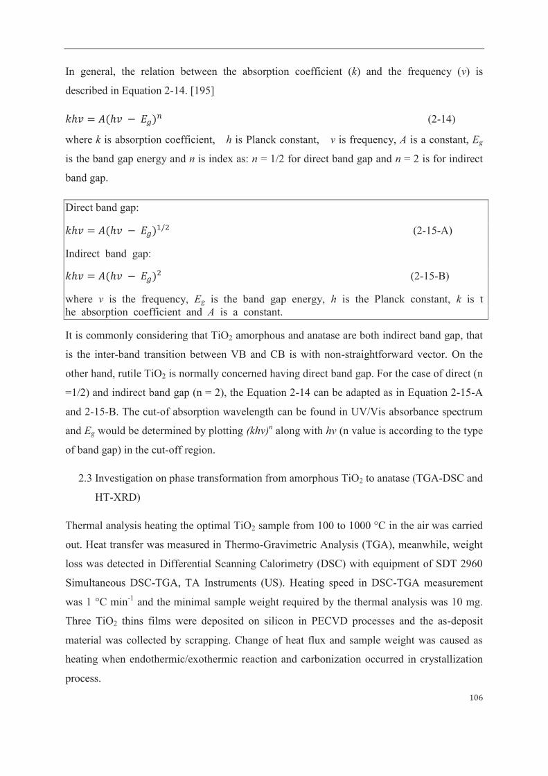
106
In general, the relation between the absorption coefficient (k) and the frequency (ν) is
described in Equation 2-14. [195]
J$2 = FM$2# .#&'O- (2-14)
where k is absorption coefficient, h is Planck constant, ν is frequency, A is a constant, Eg
is the band gap energy and n is index as: n = 1/2 for direct band gap and n = 2 is for indirect
band gap.
Direct band gap:
J$2 = FM$2# .#&'OS�k (2-15-A)
Indirect band gap:
J$2 = FM$2# .#&'Ok (2-15-B)
where v is the frequency, Eg is the band gap energy, h is the Planck constant, k is the absorption coefficient and A is a constant.
It is commonly considering that TiO2 amorphous and anatase are both indirect band gap, that
is the inter-band transition between VB and CB is with non-straightforward vector. On the
other hand, rutile TiO2 is normally concerned having direct band gap. For the case of direct (n
=1/2) and indirect band gap (n = 2), the Equation 2-14 can be adapted as in Equation 2-15-A
and 2-15-B. The cut-of absorption wavelength can be found in UV/Vis absorbance spectrum
and Eg would be determined by plotting (khv)n along with hv (n value is according to the type
of band gap) in the cut-off region.
2.3 Investigation on phase transformation from amorphous TiO2 to anatase (TGA-DSC and
HT-XRD)
Thermal analysis heating the optimal TiO2 sample from 100 to 1000 °C in the air was carried
out. Heat transfer was measured in Thermo-Gravimetric Analysis (TGA), meanwhile, weight
loss was detected in Differential Scanning Calorimetry (DSC) with equipment of SDT 2960
Simultaneous DSC-TGA, TA Instruments (US). Heating speed in DSC-TGA measurement
was 1 °C min-1 and the minimal sample weight required by the thermal analysis was 10 mg.
Three TiO2 thins films were deposited on silicon in PECVD processes and the as-deposit
material was collected by scrapping. Change of heat flux and sample weight was caused as
heating when endothermic/exothermic reaction and carbonization occurred in crystallization
process.
107
In parallel, high-temperature X-ray diffraction (HT-XRD) of X'pert Pro, Pan Analytical
(Netherland) was applied to track the crystallization evolution by heating TiO2 from 100 to
700 °C. Incident X-ray and measuring parameters were the same as the room temperature
XRD method (described in session 1.2 in this chapter). An in-situ furnace is compacted under
the sample holder in the diffractometer. Heating program used in HT-XRD analysis is
illustrated in Figure 2-9. Heating and cooling rate were controlled as 1 and 10 °C min-1
respectively. XRD measurement took place at each increased 100 °C and the measurement
lasted 25 minutes each time. Appearance and development of diffraction peaks (related to
crystal faces) were observed when the measuring temperatures increased.
Fig. 2-9 High-temperature X-ray diffraction (HT-XRD) heating program.
3 Characterization on functional properties of TiO2 films
Anatase TiO2 thin films have been synthesized in PECVD process combined with
post-annealing. After their physico-chemical properties were characterized, functional
photocatalytic activity was assessed with various methods. The assessments included
self-cleaning surface test (Pilkington protocol) for silicon-supported TiO2 samples and
diffusion test and membrane performance for ceramic-supported TiO2 samples. Effect of
preparation conditions (substrate and post-annealing temperatures) on photoactive efficiency
was compared in “static” Pilkington test. Optimal anatase films on porous ceramic were
examined in diffusion cell and pilot plants with “dynamic” conditions. UV source, model
compound, initial concentration and applied pressure were investigated as variable parameters
in the different tests.

108
3.1 Photocatalytic activity measurement in “static” conditions
Pilkington protocol was published in a patent, in which a fatty acid (stearic acid) was attached
to TiO2 surface and the adhered wax-like acid was removed from the surface under UV
illumination. [196] Quantity of stearic acid remained on the surface was analyzed in infrared
absorbance spectra as a function of UV illuminating duration.
3.1.1 Model compound, TiO2 film and UV lamp
Stearic acid, from Sigma-Aldrich (Germany), was used as the model compound in
self-cleaning surface test. Chemical structure of stearic acid (IUPAC name octadecanoic acid)
is given in Figure 2-10. Molecular formula of stearic acid is CH3(CH2)16CO2H with molar
mass 284.48 g mol-1, density 847.0 kg m-3 and boiling point 376.1 °C. 0.25 g powder of
stearic acid was diluted in 100 ml methanol and the solution of concentration 8.8 × 10⁻³ mol
L-1 was prepared.
Fig. 2-10 Chemical structure of stearic acid.
PECVD TiO2 films were deposited on silicon at substrate temperature at 50, 150 and 250 °C
with other parameters kept constant. Post-thermal treatment was made at 400 °C so that
anatase could be formed in the films. Virgin silicon and TiO2-coated silicon were dipped into
the prepared stearic acid solution (c = 8.8 × 10⁻³ mol L-1) manually with hands. They were
immersed in the solution for a few seconds and then drew out afterward. The wetted samples
were dried in the air and then white wax-like stearic acid was adhered on the surface. Such
organic compound attached silicon and TiO2 surfaces were ready for self-cleaning
experiment.
UV source was provided from four tubular CLEO compact lamps from Philips (Netherland)
arrayed in a Eurosolar box. The lamp emits highly concentrated radiation in the range 300 –
400 nm, whose emission spectrum is presented in Figure 2-11 (provided by the lamp
manufacturer). Total irradiation intensity of the new furnished UV lamp was 50 W m-2 with a
main peak at wavelength 355 nm.

109
Fig. 2-11 Emission spectrum of the UV source (CLEO fluorescent lamp).[197]
A photo of the CLEO compacted lamp (arrayed in a box) is displayed in Figure 2-12. Since
the tubular lamps would be aged by long-term use, irradiation intensity in the real-time could
be measured by a radiometer of UVICURE®, Electronic Instrumentation and Technology
(USA) that is shown on the left hand in the photo.
Fig. 2-12 Photo of CLEO compacted lamp with its irradiation intensity measure by a
radiometer.
3.1.2 Pilkington test
Pilkington protocol was established to evaluate UV illuminated TiO2 surface’s
photodegradation capability on the selected model compound stearic acid. Stearic acid has an

110
18-carbon chain and is rich in C-H bond that can be characteristically detected in infrared
spectroscopy. The organic molecules were immobilized on TiO2 surface by dip coating in
stearic acid solution (c = 8.8 × 10⁻³ mol L-1). The assessment protocol is graphically depicted
in Figure 2-13. It is a simple method since the analysis is done by a fast infrared absorbance
measurement on the solid surface. The dip-coated sample was placed under the UV lamp with
distance 30 cm. With each 10-minute UV irradiation the dip-coated sample was analyzed in
FTIR (with the same operation as described in session 1.2 in this chapter). Infrared absorption
spectra were recorded from wavenumber 500 to 4000 cm-1 along with illumination duration.
Eventually, the amount of stearic acid molecules remained on TiO2 surface was
proportionally analyzed and compared according to the infrared spectra.
Fig. 2-13 Schematic presentation of Pilkington test.
In principle, intensity of C–H vibration (specified wavenumber 2800 – 3000 cm-1) detected in
FTIR is proportional to the number of stearic acid molecules present on the sample surface.
The peak area at wavenumber 2800 – 3000 cm-1 was integrated in Omnic program. Decline of
the C-H band area (A) was quantified as a function of UV irradiation time. Then
photodegradation rate (RST) of stearic acid by illuminated TiO2 was determined as in Equation
2-16.
Photodegrading conversion rate (RST):
��� = MN . F;FuO × Nuu� (2-16)
where t is the UV irradiation duration, A0 is the initial peak area of C-H vibration (2
800 – 3000 cm-1) in FTIR spectrum and At is the studied peak area at time t.
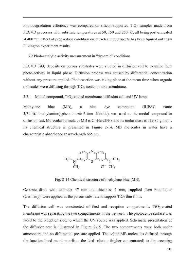
111
Photodegradation efficiency was compared on silicon-supported TiO2 samples made from
PECVD processes with substrate temperatures at 50, 150 and 250 °C, all being post-annealed
at 400 °C. Effect of preparation condition on self-cleaning property has been figured out from
Pilkington experiment results.
3.2 Photocatalytic activity measurement in “dynamic” conditions
PECVD TiO2 deposits on porous substrates were studied in diffusion cell to examine their
photo-activity in liquid phase. Diffusion process was caused by differential concentration
without any pressure applied. Photoreaction was taking place at the mean time when organic
molecules were diffusing through TiO2-coated porous membrane.
3.2.1 Model compound, TiO2-coated membrane, diffusion cell and UV lamp
Methylene blue (MB), a blue dye compound (IUPAC name
3,7-bis(dimethylamino)-phenothiazin-5-ium chloride), was used as the model compound in
diffusion test. Molecular formula of MB is C16H18ClN3S and its molar mass is 319.85 g mol-1.
Its chemical structure is presented in Figure 2-14. MB molecules in water have a
characteristic absorbance at wavelength 665 nm.
Fig. 2-14 Chemical structure of methylene blue (MB).
Ceramic disks with diameter 47 mm and thickness 1 mm, supplied from Fraunhofer
(Germany), were applied as the porous substrate to support TiO2 thin films.
The diffusion cell was constructed of feed and reception compartments. TiO2-coated
membrane was separating the two compartments in the between. The photoactive surface was
faced to the reception side, to which the UV source was applied. Schematic presentation of
the diffusion test is illustrated in Figure 2-15. The two compartments were both under
atmosphere and no differential pressure applied. The solute MB molecules diffused through
the functionalized membrane from the feed solution (higher concentrated) to the accepting

112
solution (lower concentrated), meanwhile photoreaction occurred on the reception side with
UV irradiation.
Fig. 2-15 Configuration of the diffusion cell. [14]
The employed UV lamp is the same one as described in Pilkington test (seen in session 3.1 in
this chapter). Yet four new tubular CLEO compact lamps, from the same manufacturer
(Philips, Netherland), were replacing the aged ones. Radiometer UVICURE® from Electronic
Instrumentation and Technology (USA) was used to measure the real-time intensity of the
new fluorescent lamps, which was found at 55 W m-2 (with main peak at wavelength 355
nm).
3.2.2 Diffusion test
Mother solution of MB of concentration 1×10⁻³ mol L-1 was prepared with dissolving 0.0320
g MB powders in 100 ml water (from Millipore). By diluting the mother solution, a series of
solution with concentration 1×10⁻⁶, 2×10⁻⁶, 4×10⁻⁶, 6×10⁻⁶, 8×10⁻⁶ and 1×10⁻⁵ mol L-1 were
derived. Absorbance spectrum of MB solution (c = 1×10⁻⁵ mol L-1) was measured with
UV/Vis spectroscope and maximum absorption intensity was found at wavelength 665 nm.
Calibration curve was made by plotting the aspect absorption intensity (at 665 nm) as a
function of concentration of the diluted solutions (from 10-6 to 10-5 mol L-1).
Light interaction in a material is explained in Lambert-Beer law as given in Equation 2-17,
where light transmission (T) is related to concentration of solution. When absorbance (A) is
defined as –ln(I/I0) as written in Equation 2-18, A is in a linear relationship with concentration

113
(C) as expressed in Equation 2-19. With this principle, MB concentration was calculated from
the UV/Vis absorbance intensity (determined with UV/Vis spectrometry V-570, JASCO, at
665 nm corresponding to the maximum absorbance by MB) with knowing the calibrated
linear relationship slope.
Lambert-Beer law:
]{�v= ��u = !.��P (2-17)
F�{v = .�\#M ��uO = ��P (2-18)
where I0 and I are the intensity of incident and transmitted light, Tsm. is the transmittance,
Abs. is the absorbance, ε is the molar extinction coefficient, l is the light path length and C is
the solution concentration.
Then,
P = F�{vJ (2-19)
where C is the solution concentration, Abs is the absorbance and k is the factor as k = εl.
In order to characterize the photocatalytic activity of TiO2-Al2O3 composite membrane M100
and M800 in diffusion conditions, degradation tests using methylene blue (MB) in water
solution were performed in a lab-scale diffusion cell. TiO2-coated membrane was integrated
in middle of the diffusion cell with photoactive layer facing to the reception side. The ceramic
support was also tested under the same conditions to check the self-photolysis contribution.
The diffusion cell (seen in the photo of Figure 2-16) consisted of two borosilicate glass tanks
of volume 90 mL separated with the flat membrane of membrane surface area equal to 12.56
cm2. As a remark, it can be noted that borosilicate glass cuts most of the radiation under 400
nm and, considering the emission spectrum (Figure 2-11), better performance could be
expected using a quartz cell (or a source emitting at higher wavelength, as a solar simulator).
The feed tank contained the aqueous solution of MB (C0 = 10−4 mol /L); the reception tank
was initially filled with pure water. After a first stage with a contact time of one day in order

114
to saturate the pore surface in the membrane with adsorbed organic molecules, the feed and
reception tanks were replaced by fresh aqueous solution and pure water respectively. Starting
time (t = 0) was accounted immediately. Equivalent duration of alternative period of 1 h in the
absence of UV irradiation and of 1 h in the presence of UV irradiation was operated. Increase
of organic concentration in the reception tank can be caused by diffusion in the un-irradiated
period, whereas, decrease of the concentration can be found due to photo-degradation in spite
of continuous diffusion transport. The UV irradiation was applied at a distance of 20 cm from
the anatase-coated side of the membrane placed in contact with the reception solution. UV
specific power and wavelength were 35 W m-2 and 365 nm, respectively.
Fig. 2-16 Photos of the diffusion test with UV lamp off (up) and on (bottom).
Three samples of TiO2 layer (a few μm thick) coated ceramic membrane were prepared from
optimal PECVD process combined with post-annealing. They were examined in the diffusion
test using MB feed solution of initial concentration 1×10⁻⁴ mol L-1. Two samples of TiO2 skin
(hundreds of nm thick) coated ceramic membrane were also investigated in the same way.
Each of the samples was tested three to four times to investigate reproducible performance.

115
3.3 Material and method for membrane performance in photocatalytic membrane reactor
(PMR)
Membrane performance in terms of permeation ability and photocatalytic property has been
investigated performing dynamic tests (differential pressure ΔP in the range 0.1 – 1.0 bar)
with TiO2-coated ceramic membranes integrated in a PMR process. Two kinds of PMR were
used. In the first configuration (lab-scale) implemented at ITM-CNR (University of Calabria,
Rende, Italy), 60 mL solution was circulated in the loop of the PMR system with permeation
returning to the feed. In the second configuration (pilot-scale) implemented at IEM
(University of Montpellier, France), 3 L solution was running in the PMR system with
permeation separating away from the system.
Before any photocatalytic performance test, volume flux of water Jwater (L m-2 s-1) through the
prepared membrane was measured at different pressure DP as calculated in Equation 2-20:
Water flux through the membrane:
E�0?Q@ = ���;!<B;#� (2-20)
where Jwater is flux of water through the membrane, Vwater is the permeated volume of water
(V = 0.05 L), Δt is the duration measured for 0.05 L water flowing through and S is the
membrane surface area (S = 0.126 m2).
3.3.1 Lab-scale PMR (ITM-CNR)
Acid orange 7 (AO7) from Sigma-Aldrich (Germany), IUPAC name sodium
4-[(2E)-2-(2-oxonaphthalen-1-ylidene)hydrazinyl]benzenesulfonate, has been chosen as the
model compound in the lab-scale PMR test. Molecular formula of AO7 is C16H11N2NaO4S
and its molar mass 350.32 g mol-1. Its chemical structure is presented in Figure 2-17.
Absorbance spectrum of AO7 molecules in water was recorded with UV/Vis spectroscopy
and maximum absorbance intensity was found at wavelength 485 nm. Calibration was made
by plotting absorbance intensity at 485 nm as function of concentration of AO7 solution
(from 10-6 to 10-5 mol L-1).
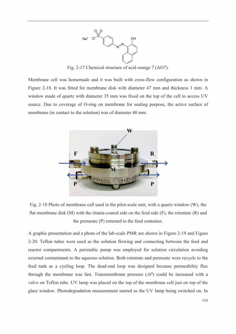
116
Fig. 2-17 Chemical structure of acid orange 7 (AO7).
Membrane cell was homemade and it was built with cross-flow configuration as shown in
Figure 2-18. It was fitted for membrane disk with diameter 47 mm and thickness 1 mm. A
window made of quartz with diameter 35 mm was fixed on the top of the cell to access UV
source. Due to coverage of O-ring on membrane for sealing purpose, the active surface of
membrane (in contact to the solution) was of diameter 40 mm.
Fig. 2-18 Photo of membrane cell used in the pilot-scale unit, with a quartz window (W), the
flat membrane disk (M) with the titania-coated side on the feed side (F), the retentate (R) and
the permeate (P) returned to the feed container.
A graphic presentation and a photo of the lab-scale PMR are shown in Figure 2-19 and Figure
2-20. Teflon tubes were used as the solution flowing and connecting between the feed and
reactor compartments. A peristaltic pump was employed for solution circulation avoiding
external contaminant to the aqueous solution. Both retentate and permeate were recycle to the
feed tank as a cycling loop. The dead-end loop was designed because permeability flux
through the membrane was fast. Transmembrane pressure (ΔP) could be increased with a
valve on Teflon tube. UV lamp was placed on the top of the membrane cell just on top of the
glass window. Photodegradation measurement started as the UV lamp being switched on. In

117
total initial volume of 60 mL was used as the feed and sampling solution of 1.5 mL was taken
from he feed tank every 10 minutes. The solution was analyzed with its absorbance at λ = 485
nm in UV/Vis spectrometry. The analyzed solution was wasted then. Mass balance is
considered throughout the process lasting for 2 hours.
Fig. 2-19 Lab-scale PMR with permeation circulating in the loop.
Fig. 2-20 Photo of the lab-scale PMR apparatus with a dead-end cycling.
An alternative configuration of the membrane cell was worked with TiO2 layer in contact with
the feed solution as schematically presented in Figure 2-21. The applied pressure on
membrane surface of TiO2 layer could increase sorption capacity on the photoactive layer as
in Langmuir’s adsorption model. Products and by-products from the organic solute’s

118
photodegradation can exist in the permeate flow. In the experiment, retention and permeation
solutions are both circulated back to the feed tank (being stirred all the time) throughout the
photodegradation test.
Fig. 2-21 Configuration of TiO2 photoactive coating in contact with feed solution in
photocatalytic membrane reactor (PMR).
Two types of UV source with intensity either 4 W or 500 W were studied in the PMR
operation. The low power (4 W) compact UV lamp from UVP (Germany) emits wavelength
at 254 nm, 365nm or a combination of both wavelengths. This lamp is lightweight and safe
for free hand use. In the experiment, it was placed on contact to the top of membrane cell
parallel to the quartz window. The distance between the lamp and TiO2 surface on membrane
was 5 cm. The high-intensity 500 W lamp was form Helios Italquartz srl (Italy), having
models as Zs (UVA emission at 360 nm and ozone free) and Zp (including UVA, UVB and
UVC emission). The high-intensity lamp had to be operated in a sealed chamber for security
reason. The distance between the lamp and membrane was 30 cm.
TiO2-Al2O3 composite membranes LF100 and LF800 were prepared in PECVD process by
Master internship student Li, F. Membrane LF100-a and LF100-b were deposited on alumina
support of pore size 100 nm with deposition equal to 20 and 40 min respectively. Membrane
LF800-a and LF800-b were deposited on alumina support of pore size 800 nm with
deposition equal to 20 and 40 min respectively. First of all, water permeance was measured in
the lab-scale unit using 60 mL deionized water with constant circulation speed 40 mL min-1 at
pressure 0.3, 0.5 and 0.7 for M100 membranes and at 0.05, 0.10 and 0.15 bar for LF100 and

119
LF800 membranes. Then the photodegradation test was operated using 60 ml AO7 solution of
initial concentration C0 = 1×10⁻⁴ mol L-1 as the feed for each test in lab-scale unit.
By considering the mass balance of AO7 solute (in mol), the remaining amount of AO7 in the
feed tank (Mt) can be known as in the Equation 2-21 taking account of the concentration in
the feed tank (Ci) and the extrated solution volume (Vi).
The amount of AO7 in the mixing feed tank:
�? = ����u-����:�����# (2-21)
where Ci is measured concentration of AO7 solution in the feed tank (well-mixed) at instant
UV irradiation time (when t = 0 initially C0 = 1×10⁻⁴ mol/L), V0 is the initial volume of AO7
feed solution (V0 = 60 ml), and Vi is the extracted sampling volume of AO7 solution
(separated from feed tank) at instant time (Vi = 1 mL).
Accordingly, photodegradation rate of AO7 (RAO7) by can be calculated with comparing
initial amount and the amoung at instant illumination time as given in Equation 2-22.
Photodegrading conversion rate of AO7 (RAO7):
���� = WN . �;�uY × Nuu� (2-22)
where M0 is the initial amount of AO7 (mol) in the feed solution and Mt is the total amount
of AO7 (mol) in the mixed feed solution at instant UV irradiation time (Mt is know from
mass balance calculation in the system as described in Equation 2-21).
The feed tank was kept in a water thermal bath whose temperature was constantly maintained.
The peristaltic pump controlled feeding flow rate at 30, 40 and 50 mL min-1 and its effect on
membrane performance was studied. TMP was experimented from 0.05 to 0.70 bar and its
effect on photodegradation efficiency was also evaluated. TMP at 0.3, 0.5 and 0.7 bar was
applied when using TiO2-layer (a few μm thick) coated membrane. TMP at 0.05, 0.10 and
0.15 bar was applied when using TiO2-skin (hundreds of nm thick) coated membrane. No
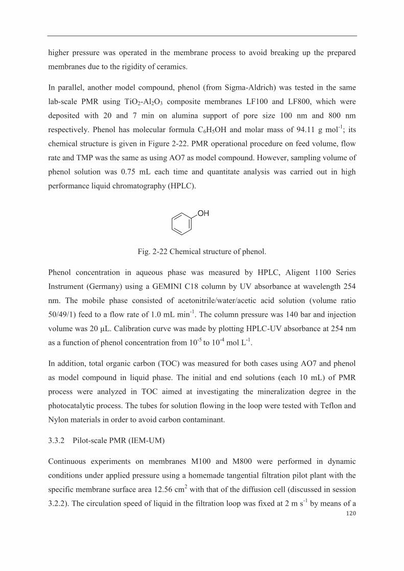
120
higher pressure was operated in the membrane process to avoid breaking up the prepared
membranes due to the rigidity of ceramics.
In parallel, another model compound, phenol (from Sigma-Aldrich) was tested in the same
lab-scale PMR using TiO2-Al2O3 composite membranes LF100 and LF800, which were
deposited with 20 and 7 min on alumina support of pore size 100 nm and 800 nm
respectively. Phenol has molecular formula C6H5OH and molar mass of 94.11 g mol-1; its
chemical structure is given in Figure 2-22. PMR operational procedure on feed volume, flow
rate and TMP was the same as using AO7 as model compound. However, sampling volume of
phenol solution was 0.75 mL each time and quantitate analysis was carried out in high
performance liquid chromatography (HPLC).
Fig. 2-22 Chemical structure of phenol.
Phenol concentration in aqueous phase was measured by HPLC, Aligent 1100 Series
Instrument (Germany) using a GEMINI C18 column by UV absorbance at wavelength 254
nm. The mobile phase consisted of acetonitrile/water/acetic acid solution (volume ratio
50/49/1) feed to a flow rate of 1.0 mL min-1. The column pressure was 140 bar and injection
volume was 20 μL. Calibration curve was made by plotting HPLC-UV absorbance at 254 nm
as a function of phenol concentration from 10-5 to 10-4 mol L-1.
In addition, total organic carbon (TOC) was measured for both cases using AO7 and phenol
as model compound in liquid phase. The initial and end solutions (each 10 mL) of PMR
process were analyzed in TOC aimed at investigating the mineralization degree in the
photocatalytic process. The tubes for solution flowing in the loop were tested with Teflon and
Nylon materials in order to avoid carbon contaminant.
3.3.2 Pilot-scale PMR (IEM-UM)
Continuous experiments on membranes M100 and M800 were performed in dynamic
conditions under applied pressure using a homemade tangential filtration pilot plant with the
specific membrane surface area 12.56 cm2 with that of the diffusion cell (discussed in session
3.2.2). The circulation speed of liquid in the filtration loop was fixed at 2 m s-1 by means of a

121
circulation pump. Configuration of membrane implantation in the pilot cell is schematically
presented in Figure 2-23 with photoactive TiO2 layer implanted with a contact to permeate
solution. In the experiment, retentate solution is circulated back to the feed tank but the
permeation solution would be flowing separately away from the feed source.
By performing such reactor configuration, organic solutes that could pass through the porous
membrane could be mineralized into final products as water and carbon oxide due to
photocatalysis effect with UV illuminating. Yet low-level polluted solution is normally
required as the feed using this configuration since the contact time between transported
organic contaminants and TiO2 surface is instant as the permeate is flowing away from the
loop.
Fig. 2-23 Configuration of TiO2 photoactive surface in contact with permeate solution in
photocatalytic membrane reactor (PMR).
Model compound (methylene blue), TiO2-Al2O3 composite membranes and UV lamp
consisted in the pilot-scale unit were the same ones used in the previous diffusion test (seen in
session 3.2.1 in this chapter). Configuration of the cross-flow membrane cell used in the pilot
is schematically presented in Figure 2-24.

122
Fig. 2-24 Membrane cell of the pilot-scale unit, with a borosilicate window (W), the flat
membrane disk (M) with the titania-coated side on the permeate side, the retentate (R)
returned to the feed tank in the pilot loop, and the permeate (P) extracted with the tube from
the membrane cell.
Schematic presentation and a photo of the pilot-scale PMR are both given in Figure 2-25
respectively. A vertically positioned membrane cell was implanted since the feed tank and
metal tubes for liquid flowing were constructed in a up-and-down streaming configuration.
The pilot set-up was more space-saved in this arrangement. Compressed air was introduced to
the feed tank to increase the pressure in the closed system. Transmembrane pressure (TMP)
worked from 0.25 to 0.75 bar in the experiment (no higher due to the risk of breaking the
ceramic membrane). Retentate was recycled to the feed while permeate was separated apart.
Fig. 2-25 Pilot-scale PMR: schematic graph (left) and photo (right).
123
Both membrane types of M100 and M800 were experimented in the pressure-dirven
photocatalytic membrane process using the pilot-scale unit. First of all, pure water permeance
through the membranes was measured under pressure from 0.25 to 0.75 bar. Then the
photodecomposition tests were operated with the CLEO UV lamp with a distance 20 cm to
the membrane cell’s window glass. 2.5 L feed solution for each running test. Initial
concentration of MB feed solution C0 = 3.2 × 10⁻⁷ and C0 = 1.25×10⁻⁷ mol L-1 has been
respectively used for membrane M100 and M800 with constant ΔP = 0.25 bar in the process.
UV illumination is continuously supplied from the permeate side. Concentration of the
permeate solution (Cpilot) was analyzed each 5 minutes with the solution absorbance at λ =
485 nm. One photodegradation test completed when 2.5 L feed solution consumed up. Three
repetition tests for one membrane were made to prove performance stability. And for each
type of the TiO2-coated membranes, duplicate samples were examined in the PMR process to
confirm on reproducibility.
In the dynamic conditions, concentration of MB in the feed (C) leading to a complete
photodegradation is equal to dMB over water flux (Jwater) as C = δMB/Jwater, where dMB
parameter is known from the diffusion experiment. Then the expected photodegradation ratio
(RExp) can be assumed with comparing C and C0 (initial concentration in the pilot) as
described Equation 2-23.
Expected photodegradation rate (RExp):
�81� = PPu × #Nuu�# =
D�x E��;!<�Pu × #Nuu� (2-23)
where RExp is the expected photodegradation rate of MB, C0 is the concentration of MB feed
in the pilot and C is theoretical concentration dependent on δMB parameter (photodegrading
capacity of the membrane) and Jwater is the water flux through the membrane at ΔP.
In the experiment using the pilot-scale unit, photodegrading performance was evaluated on
membranes M100 and M800. The experimental degradation rate of MB (RMB) by the
illuminated membranes was obtained as Equation 2-24.

124
Experimental photodegrading conversion rate (RMB):
��) = WN . P� ¡z;Pu Y × #Nuu� (2-24)
where RMB is the measured conversion rate in the pilot, C0 is MB initial concentration of the
feed in the pilot and Cpilot is measured concentration of permeated MB solution through the
membrane under continuous UV irradiation.
Information on all the UV lamps used in the photocatalytic tests is summarized in Table 2-7.
Radiance intensity (referring the amount of photons emitted per unit surface area) from the
powered UV lamp was measured with a radiometer at a distance corresponding to the distance
between lamp and glass window on the membrane cell.
Table 20-7 Summary of UV lamp parameters (applied in the experiments).
On the basis of the experimental details presented in this chapter, physico-chemical and
functional properties of the films have been investigated. Films properties will be presented
and discussed in the following chapters.
UV lamp
Radiance intensity
(measured by
radiometer in lab)
Radiating
wavelength Manufacturer
CLEO compact UV lamp
50 W m-2 355 nm Philips (Netherland)
UV polymeration
equipment Zp
760 W m-2 180 nm – visible Helios Italquartz srl
(Italy)
UV polymeration
equipment Zs
760 W m-2 360 nm Helios Italquartz srl
(Italy)
Compact UV lamp
18 W m-2
365 nm or
254 nm
UVP (Germany)

125
Chapter III Physico-chemical properties of TiO2 material
PECVD preparation approach of amorphous TiO2 thin film has been optimized with substrate
temperature (Ts), partial pressure of argon + precursor, plasma distance and RF power
intensity. Characterization of the synthesis material is explained in this Chapter. Phase
transformation of TiO2 from amorphous to anatase is attained by post-annealing treatment,
which has been decided with the crystallization kinetic analysis.
1 Optimization on PECVD operating conditions
Plasma deposition process was initiated to prepare TiO2 thin film using the PECVD apparatus
presented in chapter 2. First, substrate temperature (Ts = 50 – 250 °C) was studied with its
effect on TiO2 deposition rate. For this study, partial pressure of argon and precursor
(PAr+TTIP), partial pressure of oxygen (PO2), RF discharge power and deposition duration (td)
were maintained constant. Secondly, PAr+TTIP was enhanced and td was prolonged in order to
increase deposited TiO2 thickness. Parallel, the influence of PAr + TTIP and plasma distance (dp)
on Ti-O abundance and thickness homogeneity was investigated. Finally, optimized
parameters Ts, PAr+TTIP and dp in PECVD process have been determined.
1.1 Effect of substrate temperature (Ts)
Amorphous TiO2 thin film was obtained as substrate temperature Ts restrained below 250 °C
in our applied PECVD process. Preliminary depositions were made with varying Ts (50 –
250 °C) when the other synthesis parameters kept as constant as possible. Partial pressure of
argon + precursor (PAr+TTIP) was maintained in the range 0.15 – 0.16 mbar (fluctuating
slightly) and partial pressure of O2 (PO2) was maintained at 0.17 mbar. Electric RF power was
slightly fluctuating in the range 60 – 65 W (with a fixed forwarding power equal to 250 W).
Plasma distance (dp), adjusted by the distance between the upper and bottom electrode, was
maintained at 3 cm. With these mentioned PECVD operating conditions, TiO2 films were
deposited on silicon substrate and noted as samples B1 – B5 (seen in Table 3-1).
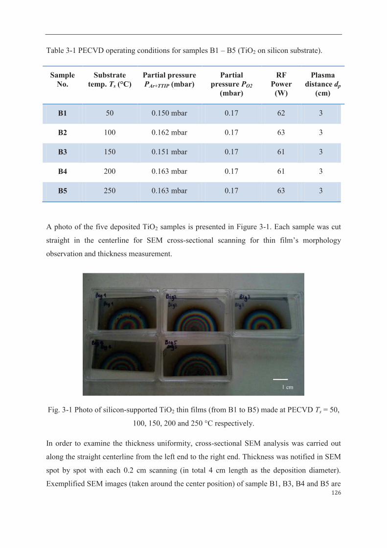
126
Table 3-1 PECVD operating conditions for samples B1 – B5 (TiO2 on silicon substrate).
Sample No.
Substrate temp. Ts (°C)
Partial pressure PAr+TTIP (mbar)
Partial pressure PO2
(mbar)
RF Power
(W)
Plasma distance dp
(cm)
B1 50 0.150 mbar 0.17 62 3
B2 100 0.162 mbar 0.17 63 3
B3 150 0.151 mbar 0.17 61 3
B4 200 0.163 mbar 0.17 61 3
B5 250 0.163 mbar 0.17 63 3
A photo of the five deposited TiO2 samples is presented in Figure 3-1. Each sample was cut
straight in the centerline for SEM cross-sectional scanning for thin film’s morphology
observation and thickness measurement.
Fig. 3-1 Photo of silicon-supported TiO2 thin films (from B1 to B5) made at PECVD Ts = 50,
100, 150, 200 and 250 °C respectively.
In order to examine the thickness uniformity, cross-sectional SEM analysis was carried out
along the straight centerline from the left end to the right end. Thickness was notified in SEM
spot by spot with each 0.2 cm scanning (in total 4 cm length as the deposition diameter).
Exemplified SEM images (taken around the center position) of sample B1, B3, B4 and B5 are

127
presented in Figure 3-2. It is apparent that PECVD TiO2 deposit has micro-columnar
structure. Moreover, uniformed TiO2 cluster in dimension ca. 10 nm (estimated from SEM) is
observed as consisting block in the thin films. The porosity of PECVD TiO2 thin film,
inherent to the columnar microstructure, is certainly advantageous for catalytic membrane
application in terms of large specific surface and high permeability.
Fig. 3-2 TiO2 thickness measured in cross-sectional SEM investigation for samples B1 to B5
deposited at different substrate temperatures from 50 to 250 °C.
Thickness profile of TiO2 (on surface of diameter equal to 4 cm) is plotted along with the
coordinate of the substrate coordinate as presented in Figure 3-3, where the coordinate
position at 2 cm is the center of the substrate. It can be seen that the deposition thickness is
symmetric as consistent to observation in the photo of the samples (shown in Figure 3-1). Due
to the geometry of gas inlet from a drilled hole in upper electrode, TiO2 layer was deposited
thicker in the center (just under the gas entrance) and thinner surrounding the edge (toward to
the outlet of the reactor). Moreover, TiO2 grew faster on surface at higher Ts (200 and 250 °C)
than that at lower Ts (50 and 150 °C). However, thickness variance (on depositing surface
12.56 cm2) obtained at higher Ts was larger than that of lower Ts as seen in Figure 3-3. The
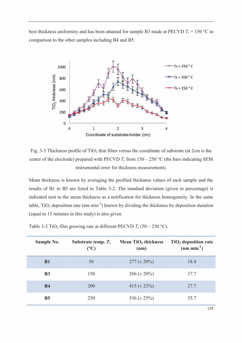
128
best thickness uniformity and has been attained for sample B3 made at PECVD Ts = 150 °C in
comparison to the other samples including B4 and B5.
Fig. 3-3 Thickness profile of TiO2 thin films versus the coordinate of substrate (at 2cm is the
center of the electrode) prepared with PECVD Ts from 150 – 250 °C (the bars indicating SEM
instrumental error for thickness measurement).
Mean thickness is known by averaging the profiled thickness values of each sample and the
results of B1 to B5 are listed in Table 3-2. The standard deviation (given in percentage) is
indicated nest to the mean thickness as a notification for thickness homogeneity. In the same
table, TiO2 deposition rate (nm min-1) known by dividing the thickness by deposition duration
(equal to 15 minutes in this study) is also given.
Table 3-2 TiO2 film growing rate at different PECVD Ts (50 – 250 °C).
Sample No. Substrate temp. Ts
(°C) Mean TiO2 thickness
(nm) TiO2 deposition rate
(nm min-1)
B1 50 277 (± 20%) 18.4
B3 150 266 (± 20%) 17.7
B4 200 415 (± 23%) 27.7
B5 250 536 (± 25%) 35.7
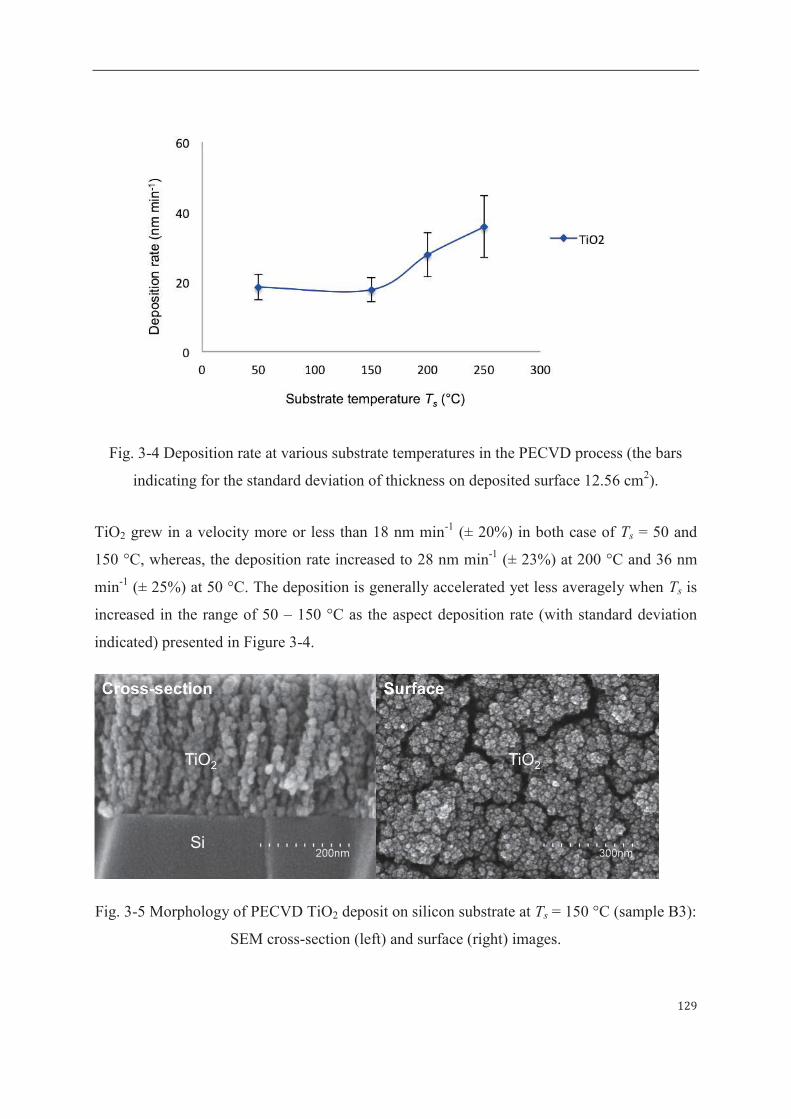
129
Fig. 3-4 Deposition rate at various substrate temperatures in the PECVD process (the bars
indicating for the standard deviation of thickness on deposited surface 12.56 cm2).
TiO2 grew in a velocity more or less than 18 nm min-1 (± 20%) in both case of Ts = 50 and
150 °C, whereas, the deposition rate increased to 28 nm min-1 (± 23%) at 200 °C and 36 nm
min-1 (± 25%) at 50 °C. The deposition is generally accelerated yet less averagely when Ts is
increased in the range of 50 – 150 °C as the aspect deposition rate (with standard deviation
indicated) presented in Figure 3-4.
Fig. 3-5 Morphology of PECVD TiO2 deposit on silicon substrate at Ts = 150 °C (sample B3):
SEM cross-section (left) and surface (right) images.

130
Zoomed SEM images of the sample B3 (deposited at Ts = 150 °C) both from the side view
and the top view are displayed in Figure 3-5. Micro-columnar porous structure and the
uniform TiO2 nanoparticles are clearly observed the presented images. Regarding to the
reasonable deposition rate and the smoothest thickness of sample B3, Ts = 150 °C has been
determined as the optimal substrate temperature in the following PECVD studies.
1.2 Influence of partial pressure (PAr+TTIP) and plasma distance (dp)
PECVD parameters including partial pressure PAr+TTIP and plasma distance dp affect the
density of gaseous molecule and ion energy distribution in the reactor. In another word, the
stability of plasma process and properties of deposited film have been studied with modifying
these two conditions. Accordingly, samples ZJ1 – ZJ9 of TiO2 deposit on silicon were
prepared by varying PAr+TTIP (0.155, 0.185 and 0.225 mbar) and dp (3.0, 2.5 and 2.0 cm), and
maintaining other PECVD parameters constant as indicated in Table 3-3. Thickness profile
(from SEM investigation) and chemical composition (from FTIR analysis) of theses samples
has been analyzed and will be discussed in the following two sections in this session.
Table 3-3 PECVD conditions (varying PAr+TTIP and dp) for TiO2 samples ZJ1 – ZJ9 (on silicon
substrate).
Sample No.
PAr+TTIP
(mbar)
Plasma distance dp
(cm)
Substrate temp. Ts
(°C)
Deposition duration
(min)
RF Power
(W)
PO2 (mbar)
ZJ1 0.155 3.0 150 20 50 0.17
ZJ2 0.185 3.0 150 20 50 0.17
ZJ3 0.225 3.0 150 20 50 0.17
ZJ4 0.155 2.5 150 20 50 0.17
ZJ5 0.185 2.5 150 20 50 0.17
ZJ6 0.225 2.5 150 20 50 0.17
ZJ7 0.155 2.0 150 20 50 0.17
ZJ8 0.185 2.0 150 20 50 0.17
ZJ9 0.225 2.0 150 20 50 0.17
1.2.1 Effect on thickness homogeneity and deposition rate
Thickness profile of samples ZJ1 – ZJ9 was studied by cross-sectional SEM, operated on
deposition centerline spot to spot every 0.5 cm along total length 4 cm (deposition diameter)

131
similar as described in session 1.1. Mean thickness averaged from the film profile is presented
in Table 3-4, where standard deviation (in percentage) on depositing surface 12 cm2 is given
in embrace. With variable PAr+TTIP and dp and constant Ts (150 °C), RF power (50 W) and
duration (20 min), deposited TiO2 films have thickness in the range 0.5 – 3.5 μm. Thickness
deviation varies from ± 7% to ± 35% from one sample to another sample, presenting the
deposition homogeneity.
Table 3-4 Mean thickness of samples ZJ1 – ZJ9 (TiO2 film on silicon substrate) prepared with
variable PAr+TTIP and dp.
dp
PAr+TTIP 3.0 cm 2.5 cm 2.0 cm
0.155 mbar 0.75 μm (± 14%)
0.559 μm (± 13%)
0.816 μm (± 35%)
0.185 mbar 0.492 μm (± 14 %)
1.275 μm (± 14%)
1.775 μm (± 30%)
0.225 mbar 1.290 μm
(± 7%) 2.880 μm (± 21%)
3.497 μm (± 28%)
It can be seen that the best homogeneity (with the least deviation ± 7 %) was obtained for
sample ZJ3 (with the highest PAr+TTIP and longest dp), whereas the worst homogeneity (with
the largest deviation ± 35 %) was depicted on sample ZJ 7 (with the lowest PAr+TTIP and
shortest dp). TiO2 deposition rate (i.e. thickness/ deposition duration) of samples ZJ1 – ZJ9 is
plotted in Figure 3-6 with the error bar indicating for thickness deviation so that effect of
PAr+TTIP and dp on layer homogeneity and deposition rate would be obvious.
As shown in Figure 3-6, higher argon flux leads to faster TiO2 growth rate due to the
increased number of TTIP vapor molecules (driven by argon flux) in the chamber. Shorter
plasma distance results in thicker deposits due to the same reason at the scale of the
inter-electrodes space (nevertheless this effect is not obvious in the case of the lowest argon
flux giving the lowest TTIP concentration whose influence on the film growth rate is certainly
slightly dependent on the plasma volume).
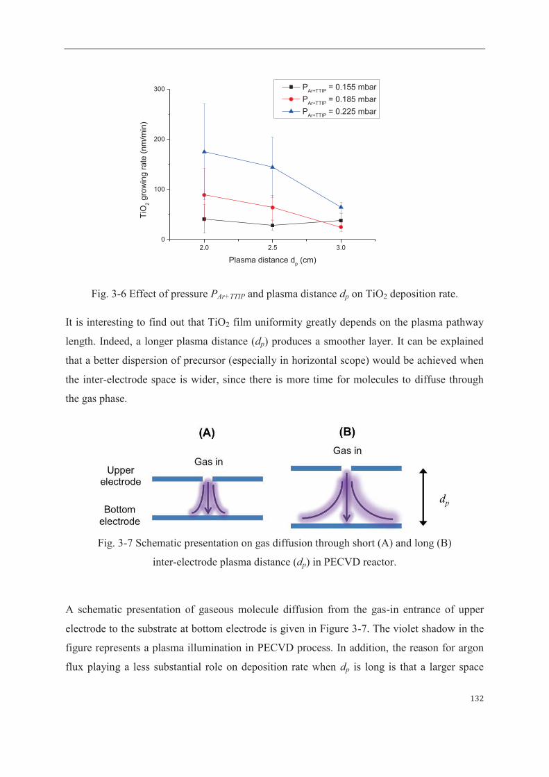
132
Fig. 3-6 Effect of pressure PAr+TTIP and plasma distance dp on TiO2 deposition rate.
It is interesting to find out that TiO2 film uniformity greatly depends on the plasma pathway
length. Indeed, a longer plasma distance (dp) produces a smoother layer. It can be explained
that a better dispersion of precursor (especially in horizontal scope) would be achieved when
the inter-electrode space is wider, since there is more time for molecules to diffuse through
the gas phase.
Fig. 3-7 Schematic presentation on gas diffusion through short (A) and long (B)
inter-electrode plasma distance (dp) in PECVD reactor.
A schematic presentation of gaseous molecule diffusion from the gas-in entrance of upper
electrode to the substrate at bottom electrode is given in Figure 3-7. The violet shadow in the
figure represents a plasma illumination in PECVD process. In addition, the reason for argon
flux playing a less substantial role on deposition rate when dp is long is that a larger space
2.0 2.5 3.0
0
100
200
300
TiO
2 g
row
ing r
ate
(nm
/min
)
Plasma distance dp (cm)
PAr+TTIP
= 0.155 mbar
PAr+TTIP
= 0.185 mbar
PAr+TTIP
= 0.225 mbar
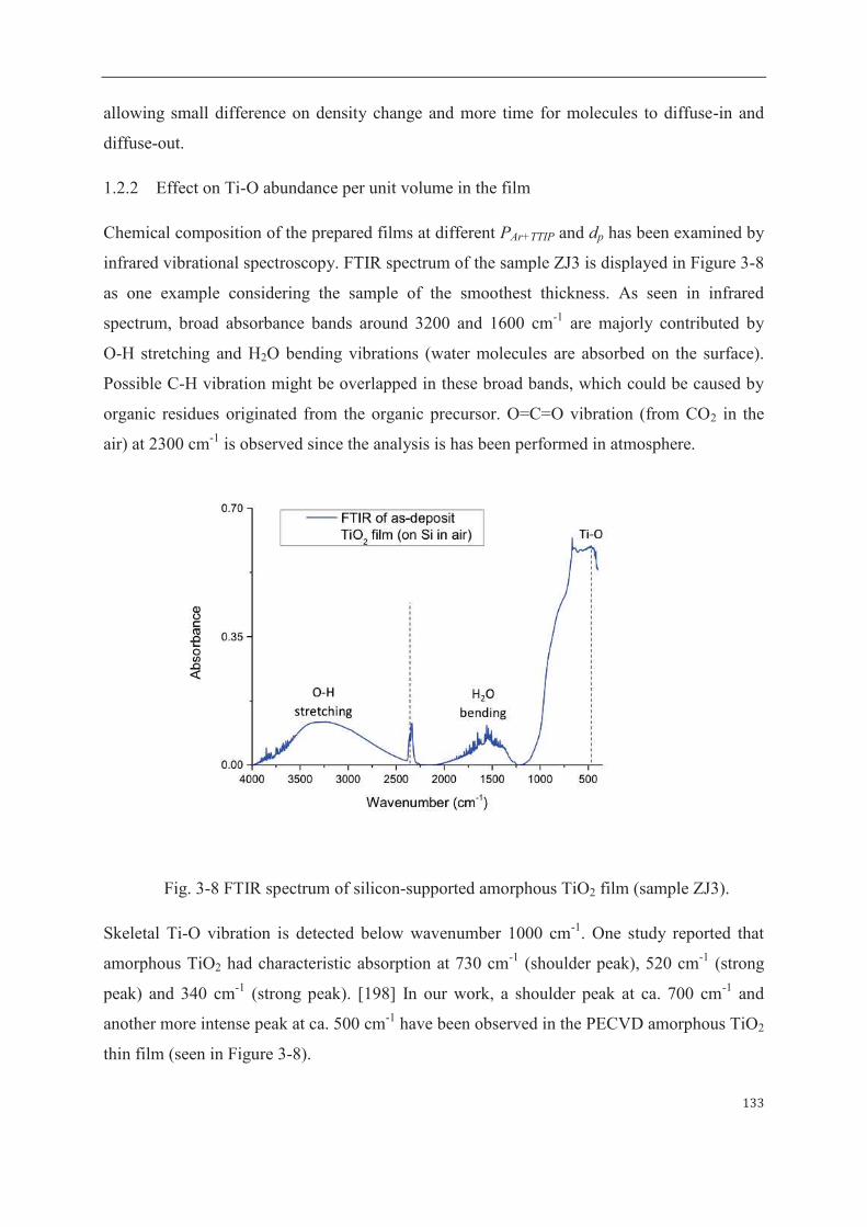
133
allowing small difference on density change and more time for molecules to diffuse-in and
diffuse-out.
1.2.2 Effect on Ti-O abundance per unit volume in the film
Chemical composition of the prepared films at different PAr+TTIP and dp has been examined by
infrared vibrational spectroscopy. FTIR spectrum of the sample ZJ3 is displayed in Figure 3-8
as one example considering the sample of the smoothest thickness. As seen in infrared
spectrum, broad absorbance bands around 3200 and 1600 cm-1 are majorly contributed by
O-H stretching and H2O bending vibrations (water molecules are absorbed on the surface).
Possible C-H vibration might be overlapped in these broad bands, which could be caused by
organic residues originated from the organic precursor. O=C=O vibration (from CO2 in the
air) at 2300 cm-1 is observed since the analysis is has been performed in atmosphere.
Fig. 3-8 FTIR spectrum of silicon-supported amorphous TiO2 film (sample ZJ3).
Skeletal Ti-O vibration is detected below wavenumber 1000 cm-1. One study reported that
amorphous TiO2 had characteristic absorption at 730 cm-1 (shoulder peak), 520 cm-1 (strong
peak) and 340 cm-1 (strong peak). [198] In our work, a shoulder peak at ca. 700 cm-1 and
another more intense peak at ca. 500 cm-1 have been observed in the PECVD amorphous TiO2
thin film (seen in Figure 3-8).

134
The absorbance intensity at 450 cm-1 was compared among the samples ZJ1 – ZJ9 from the
spectra recorded at the central spot of each deposition, where the thickness was measured in
previous SEM study. The wavenumber 450 cm-1 is found with a characteristic peak for the
annealed TiO2 samples of anatase phase (will be further explained later). Normalized
absorbance intensity at 450 cm-1 has been obtained by treating the measured absolute intensity
with a factor proportional to TiO2 thickness. Such factors for samples ZJ1-ZJ9 are listed in
Table 3-5.
Consequently, the thickness-independent Ti-O vibration can be compared as plotted in Figure
3-8. It can stand for Ti-O abundance per unit volume in the synthetic film, since absorbance
intensity of light is proportional to the number of molecules. So the highest normalized
absorbance indicates the richest Ti-O density among samples ZJ1 – ZJ9.
Table 3-5 Normalized absorbance intensity (at 450 cm-1) of TiO2 thin films prepared with
different PECVD parameters of PAr+TTIP and dp.
dp
PAr+TTIP 3.0 cm 2.5 cm 2.0 cm
0.155 mbar 0.818 1.255 2.057
0.185 mbar 1.805 2.037 1.080
0.225 mbar 4.658 1.646 0.756
As presented in Figure 3-9, PAr+TTIP and dp have apparent influence on Ti-O abundance in the
deposited film (reflected from absorbance at characteristic wavenumber 450 cm-1). With low
partial pressure PAr+TTIP = 0.155 mbar, a small decline of Ti-O composition is discovered
when elongating dp from 2 to 3 cm. In contrast, with high PAr+TTIP = 0.225 mbar Ti-O
composition surged up when extending dp to 3 cm. With medium PAr+TTIP = 0.185 mbar,
increase of Ti-O composition is found when extending dp to 2.5 cm and saturation state is
then reached when continuously enlarging dp to 3 cm. It can be explained that decomposition
is the rate-limiting step when the pressure is high, whereas, the reactant density is the
rate-limiting step when the pressure is low.
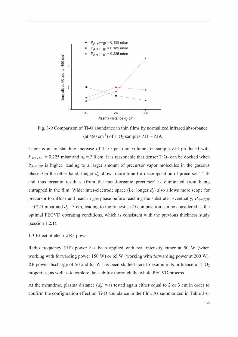
135
Fig. 3-9 Comparison of Ti-O abundance in thin films by normalized infrared absorbance
(at 450 cm-1) of TiO2 samples ZJ1 – ZJ9.
There is an outstanding increase of Ti-O per unit volume for sample ZJ3 produced with
PAr+TTIP = 0.225 mbar and dp = 3.0 cm. It is reasonable that denser TiO2 can be docked when
PAr+TTIP is higher, leading to a larger amount of precursor vapor molecules in the gaseous
phase. On the other hand, longer dp allows more time for decomposition of precursor TTIP
and thus organic residues (from the metal-organic precursor) is eliminated from being
entrapped in the film. Wider inter-electrode space (i.e. longer dp) also allows more scope for
precursor to diffuse and react in gas phase before reaching the substrate. Eventually, PAr+TTIP
= 0.225 mbar and dp =3 cm, leading to the richest Ti-O composition can be considered as the
optimal PECVD operating conditions, which is consistent with the previous thickness study
(session 1.2.1).
1.3 Effect of electric RF power
Radio frequency (RF) power has been applied with real intensity either at 50 W (when
working with forwarding power 150 W) or 65 W (working with forwarding power at 200 W).
RF power discharge of 50 and 65 W has been studied here to examine its influence of TiO2
properties, as well as to explore the stability thorough the whole PECVD process.
At the meantime, plasma distance (dp) was tested again either equal to 2 or 3 cm in order to
confirm the configuration effect on Ti-O abundance in the film. As summarized in Table 3-6,
2.0 2.5 3.0
0
2
4
6
Norm
aliz
ed IR
abs. at 450 c
m-1
Plasma distance dp(cm)
PAr+TTIP = 0.155 mbar
PAr+TTIP = 0.185 mbar
PAr+TTIP = 0.225 mbar
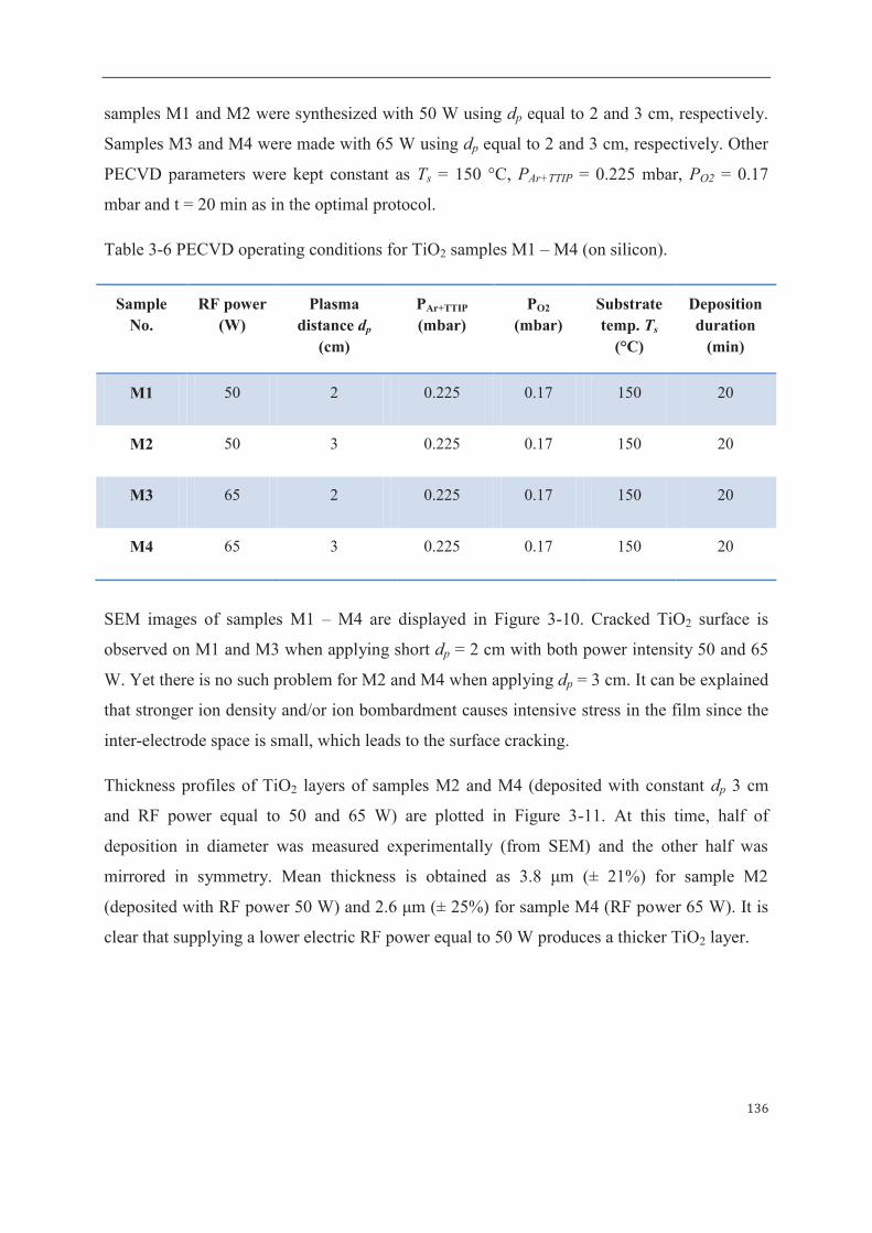
136
samples M1 and M2 were synthesized with 50 W using dp equal to 2 and 3 cm, respectively.
Samples M3 and M4 were made with 65 W using dp equal to 2 and 3 cm, respectively. Other
PECVD parameters were kept constant as Ts = 150 °C, PAr+TTIP = 0.225 mbar, PO2 = 0.17
mbar and t = 20 min as in the optimal protocol.
Table 3-6 PECVD operating conditions for TiO2 samples M1 – M4 (on silicon).
Sample No.
RF power (W)
Plasma distance dp
(cm)
PAr+TTIP (mbar)
PO2 (mbar)
Substrate temp. Ts
(°C)
Deposition duration
(min)
M1 50 2 0.225 0.17 150 20
M2 50 3 0.225 0.17 150 20
M3 65 2 0.225 0.17 150 20
M4 65 3 0.225 0.17 150 20
SEM images of samples M1 – M4 are displayed in Figure 3-10. Cracked TiO2 surface is
observed on M1 and M3 when applying short dp = 2 cm with both power intensity 50 and 65
W. Yet there is no such problem for M2 and M4 when applying dp = 3 cm. It can be explained
that stronger ion density and/or ion bombardment causes intensive stress in the film since the
inter-electrode space is small, which leads to the surface cracking.
Thickness profiles of TiO2 layers of samples M2 and M4 (deposited with constant dp 3 cm
and RF power equal to 50 and 65 W) are plotted in Figure 3-11. At this time, half of
deposition in diameter was measured experimentally (from SEM) and the other half was
mirrored in symmetry. Mean thickness is obtained as 3.8 μm (± 21%) for sample M2
(deposited with RF power 50 W) and 2.6 μm (± 25%) for sample M4 (RF power 65 W). It is
clear that supplying a lower electric RF power equal to 50 W produces a thicker TiO2 layer.

137
Fig. 3-10 SEM images of samples M1 – M4 (TiO2 on silicon) prepared with RF power 50 and
65 W and plasma distance 2 and 3 cm.
Fig. 3-11 Thickness profile of TiO2 samples prepared with constant dp = 3 cm and RF power
equal to 50 and 65 W respectively (measured by SEM of 10% instrumental error indicated
with the bars).

138
Fig. 3-12 Normalized FTIR spectra (independent from the thickness) of TiO2 thin films
deposited on silicon as samples M1 – M4.
In addition, chemical composition of samples M1 – M4 was examined by FTIR; the
corresponding normalized infrared spectra are presented in Figure 3-12. Apparent difference
on normalized vibrational absorbance in the range 700 – 500 cm-1 (thickness irrelevant) can
be witnessed in the figure. Samples M1 and M2 (obtained at 50 W) have more intensive Ti-O
abundance than that of M3 and M4 (obtained at 65 W). Besides, applying the same power
intensity, sample made with longer dp = 3 cm has more Ti-O composition than that of dp = 2
cm. Eventually, power = 50 W and dp = 3 cm is figured out as the optimized conditions for
preparing the sample with the richest Ti-O abundance per unit volume (sample M2).
Concerning the stability PECVD process lasting as long as 20 min, the RF power discharge of
intensity 50 W (from a fixed forwarding power 150 W) is preferred over 65 W (from
forwarding power 200 W). Indeed, dynamic plasma process could go through more
sparkling at 65 W during reaction and/or deposition process. In addition, more severe
carbonization of precursor occurred in the gas-in tube at 65 W maybe due to higher gas
temperature, which could cause blockage in the gas pathway.
In a summary, optimization work of preparing amorphous TiO2 thin films in PECVD process
has been studied. It is found that optimal substrate temperature Ts is equal to 150 °C leading

139
to a reasonable deposition rate and good thickness homogeneity. Further on, partial pressure
of argon and precursor PAr+TTIP = 0.225 mbar (controlled by argon flux) and plasma distance
dp = 3 cm (i.e. inter-electrode distance) have been determined as optimal values for good
thickness uniformity and rich Ti-O abundance. In addition, 50 W (obtained from forwarding
power 150 W) has been identified as optimized RF power able to maintain stable plasma
process with less carbonization of precursor. Partial pressure of oxygen PO2 = 0.17 mbar and
deposition duration t = 20 minutes appear as satisfying complementary PECVD parameters.
2 Optimization of post-annealing conditions to develop crystallized films
It has been reported that crystalline TiO2 material could be deposited spontaneously only
when Ts was heated above 450 °C in PECVD process. [25] In our work, optimal Ts = 150 °C
has been chosen to prepare TiO2 films in regarding to feasibility for thermal-sensitive
substrate. As the as-grown TiO2 films were found all in amorphous phase in the work,
post-annealing treatment on as-deposit sample was carried out in a furnace in order to
crystallize TiO2 film. The post-thermal treatment was studied both along with increased
temperatures (200 – 700 °C) and along with heating duration (1 – 6 h) at 300 °C. In the end,
seeding substrate was experimented to investigate its activity on phase transation from
amorphous to crystallized phase post-annealing at 300 °C.
2.1 Film crystallization as a function of temperature (Tp)
High-temperature X-ray diffraction (HT-XRD) analysis in the range 200 – 700 °C was made
on one optimal silicon-supported TiO2 film. The heating process is set as non-stop mode with
heating rate 1 °C min-1. X-ray diffraction pattern was recorded in-situ on the heated TiO2
sample with every increased 100 °C. Each XRD measurement took 25 minutes to complete.
HT-XRD patterns in the range 200 – 700 °C on the same sample are displayed in Figure 3-13.

140
Fig. 3-13 High-temperature XRD analysis heating from 200 to 700 °C on silicon-supported
TiO2 thin film.
It is clear that crystallization is observed in TiO2 film for post-annealing temperature at least
equal to 400 °C in HT-XRD analysis. In another word, Tp = 400 °C is the critical temperature
for crystallization when as in non-stop heating mehod. The developed crystalline structure
was found as anatase phase by matching the diffracted pattern to the database
(Anatase TiO2 phase, JCPDS No. 89–4921). The main diffraction peaks of anatase phase at 2θ =
25.4°, 37.9°, 48.1°, 54.0° and 55.1° have been detected on the 400 °C-annealed TiO2 film,
which represent the crystal planes of anatase (101), (004), (200), (115) and (211) respectively.
Enhancement of the peak intensity undergoes gradually when Tp continues to increase from
400 till 700 °C. It implies that the development of anatase crystallinity has taken place due to
higher heating temperature. Moreover, pure anatase phase was maintained in TiO2 film by
heating as high as 700 °C. In some other work, it is reported that rutile sometimes has been
formed when post-annealing above 600 °C was carried out. [14]
On the other hand, as-grown TiO2 material (on silicon) was scrubbed away from the substrate
for thermal analysis in the range 25 – 1000 °C. About 10 mg TiO2 powder was collected from
three optimized PECVD as-deposit samples. The amorphous TiO2 powder went through
thermo-gravimetric analysis (TGA) and differential scanning calorimetric (DSC) analysis by
heating it to 1000 °C in the air (with heating rate 1 °C min-1). Weight-loss curve was
measured from TGA by tracking the mass of sample. Heat-flow curve was recorded from

141
DSC by comparing the heat exchange between the sample and reference. The two curves have
been measured at the meantime and are presented in Figure 3-14.
.
Fig 3-14 Thermal analysis by heating as-deposit amorphous TiO2 material from 25 to
1000 °C.
As seen in Figure 3-14, the heat-flow curve (in blue color) witnesses an exothermic peak at
400 – 450 °C (highlighted with a grey circle). It is supposed as relevant to TiO2 phase
transition from amorphous to crystalline structure. When atoms are rearranging from random
to organized positions they would release energy in heat since it is exothermic process when
the entropy is reduced. At the meantime, the weight-loss curve (in green color) detects a
secondary loss of mass at 400 – 450 °C (highlighted with a grey circle) that follows the first
weight reduction (about 10% drop). Remove of the weight by heating below 450 °C should be
mainly caused by dehydration, dehydroxylation and removal by oxidation of residual organics
in the synthetic film. A secondary weight loss (a very small amount) occurring at 450 °C
could be explained by further release of ‘internal’ organic residues entrapped in Ti-O
framework. The liberation of “deep” trapped organic groups was realized simultaneously
when crystallization took place. The organic residues in the film were generated from the
metal-organic precursor TTIP during PECVD reaction.
0 200 400 600 800 1000 1200
0.85
0.90
0.95
1.00 Weight loss
Heat flow
Temperature (°C)
We
igh
t (%
)
-20
-10
0
Heat flow
(W
/g)
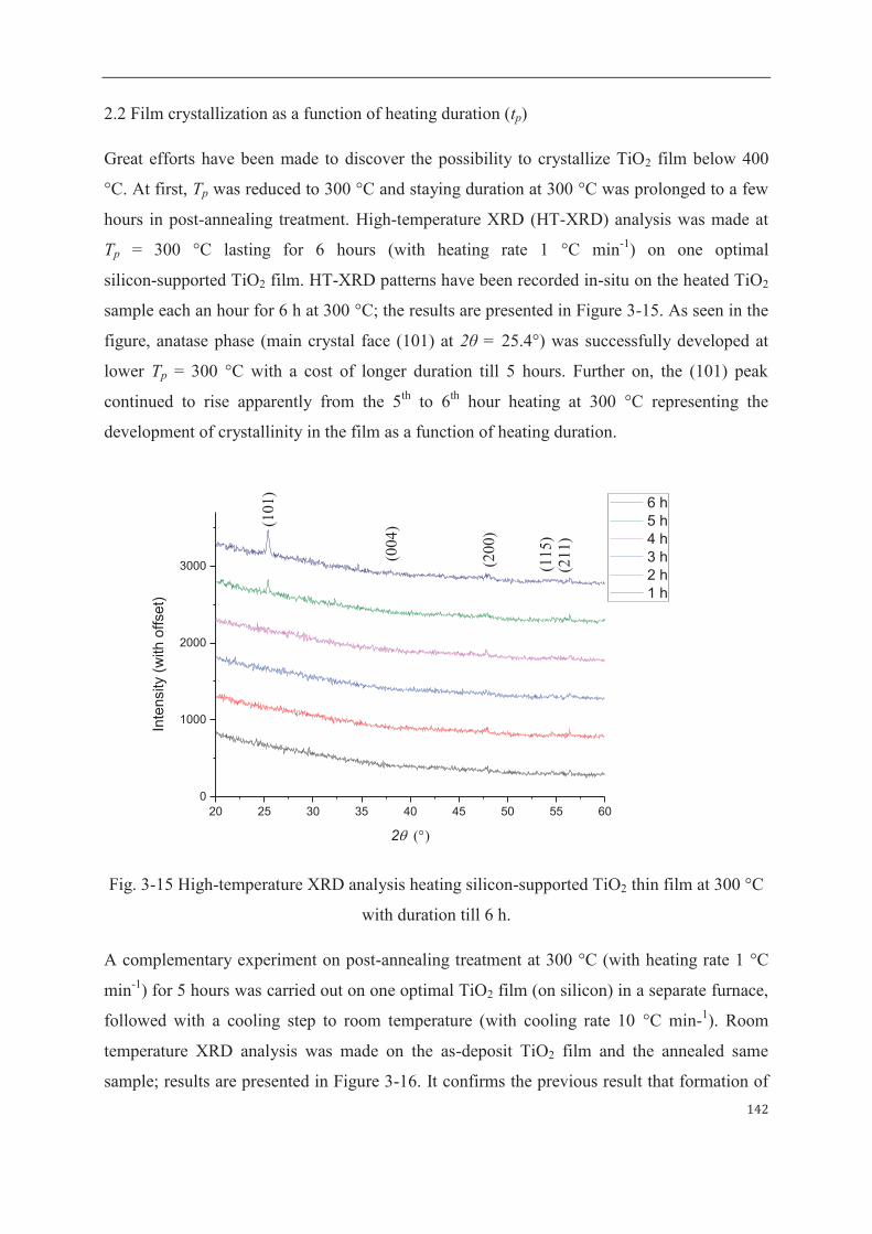
142
2.2 Film crystallization as a function of heating duration (tp)
Great efforts have been made to discover the possibility to crystallize TiO2 film below 400
°C. At first, Tp was reduced to 300 °C and staying duration at 300 °C was prolonged to a few
hours in post-annealing treatment. High-temperature XRD (HT-XRD) analysis was made at
Tp = 300 °C lasting for 6 hours (with heating rate 1 °C min-1) on one optimal
silicon-supported TiO2 film. HT-XRD patterns have been recorded in-situ on the heated TiO2
sample each an hour for 6 h at 300 °C; the results are presented in Figure 3-15. As seen in the
figure, anatase phase (main crystal face (101) at 2θ = 25.4°) was successfully developed at
lower Tp = 300 °C with a cost of longer duration till 5 hours. Further on, the (101) peak
continued to rise apparently from the 5th to 6th hour heating at 300 °C representing the
development of crystallinity in the film as a function of heating duration.
Fig. 3-15 High-temperature XRD analysis heating silicon-supported TiO2 thin film at 300 °C
with duration till 6 h.
A complementary experiment on post-annealing treatment at 300 °C (with heating rate 1 °C
min-1) for 5 hours was carried out on one optimal TiO2 film (on silicon) in a separate furnace,
followed with a cooling step to room temperature (with cooling rate 10 °C min-1). Room
temperature XRD analysis was made on the as-deposit TiO2 film and the annealed same
sample; results are presented in Figure 3-16. It confirms the previous result that formation of
20 25 30 35 40 45 50 55 60
0
1000
2000
3000
Inte
nsity (
with o
ffset)
2q (°)
6 h
5 h
4 h
3 h
2 h
1 h
(10
1)
(004
)
(20
0)
(21
1)
(11
5)

143
crystalline anatase structure has been succeeded by annealing at 300 °C within 5 hours
staying. It is noted that diffraction peaks of silicon substrate sometimes can be detected due to
the thin thickness of TiO2 layer as presented in Figure 3-15. Diffraction peaks of anatase
(101) and (004) at aspect 2θ = 25.4° and 37.9° have been indicated in the figure to be
distinguished from silicon peaks.
Fig. 3-16 XRD analysis on as-deposit and 300 °C-annealed TiO2 film deposited on silicon
substrate.
Possibility of improving crystallization of the optimal TiO2 film at 300 °C was studied by
prolonging to even longer as 10 h with a heating rate 1 °C min-1 and then a cooling rate 10 °C
min-1. Room temperature XRD patterns of both the as-deposit and 300 °C-annealed film (for
10 h) are compared in Figure 3-17.

144
Fig. 3-17 XRD on as-deposit and 300 °C-annealed TiO2 film (heated for 10 hours).
The anatase structure is more fully developed when heating at 300°C for 10 hours (Figure
3-17) in contrast to the film heated at 300°C for 5 hours (Figure 3-16). Main anatase peaks
(101), (004), (200), (115) and (211) at 2θ = 25.4°, 37.9°, 48.1°, 54.0° and 55.1° have all been
detected in the case of longer staying time of 10 hours at 300°C. Besides, another optimized
TiO2 sample (on silicon) was heated at 275°C for 24 hours but no crystal structure has been
found. It suggests that the lowest critical crystallization temperature for the synthetic TiO2
film is 300°C within 5 hours staying and that a longer staying (e.g. 10 hours) develops a better
crystallinity structure.
2.3 Seeding effect on phase transformation
A seeding layer was obtained by dip-coating the silicon substrate in sol solution that has been
mixed for 1 or 3 h. SEM images of the seeded-silicon substrate are presented in Figure 3-18.
According to the surface image, it is clear that 3-h stirred solution produced better dispersion
of seeds on silicon surface than that of 1-hour stirred one did. Sol aggregation is formed on
surface for the short-term 1 h mixed solution, whereas, well-suspended anatase nanoparticles
have been spread on surface from long-term 3 h mixed solution. Thickness of the seeding
layer is estimated ca. 60 – 70 nm as notified in the cross-sectional SEM images of Figure
3-18.

145
Figure 3-18 SEM images on nuclei seeded-silicon dip-coated from the anatase sol being
mixed for 1 hour (A and B) and 3 hours (C and, D).
Figure 3-19 Proof of anatase seeding layer: Raman spectra of silicon (left) and seeded-silicon
(right).
200 400 600
0
20000
40000
60000
Silicon
support
Inte
nsi
ty
Raman shift (cm-1)
200 400 600
0
20000
40000
60000
Seeded
silicon
Inte
nsi
ty
Raman shift (cm-1)
Anatase
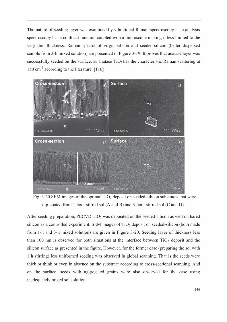
146
The nature of seeding layer was examined by vibrational Raman spectroscopy. The analysis
spectroscopy has a confocal function coupled with a microscope making it less limited to the
very thin thickness. Raman spectra of virgin silicon and seeded-silicon (better dispersed
sample from 3-h mixed solution) are presented in Figure 3-19. It proves that anatase layer was
successfully seeded on the surface, as anatase TiO2 has the characteristic Raman scattering at
150 cm-1 according to the literature. [116]
Fig. 3-20 SEM images of the optimal TiO2 deposit on seeded-silicon substrates that were
dip-coated from 1-hour stirred sol (A and B) and 3-hour stirred sol (C and D).
After seeding preparation, PECVD TiO2 was deposited on the seeded-silicon as well on bared
silicon as a controlled experiment. SEM images of TiO2 deposit on seeded-silicon (both made
from 1-h and 3-h mixed solution) are given in Figure 3-20. Seeding layer of thickness less
than 100 nm is observed for both situations at the interface between TiO2 deposit and the
silicon surface as presented in the figure. However, for the former case (preparing the sol with
1 h stirring) less uniformed seeding was observed in global scanning. That is the seeds were
thick or think or even in absence on the substrate according to cross-sectional scanning. And
on the surface, seeds with aggregated grains were also observed for the case using
inadequately mixed sol solution.
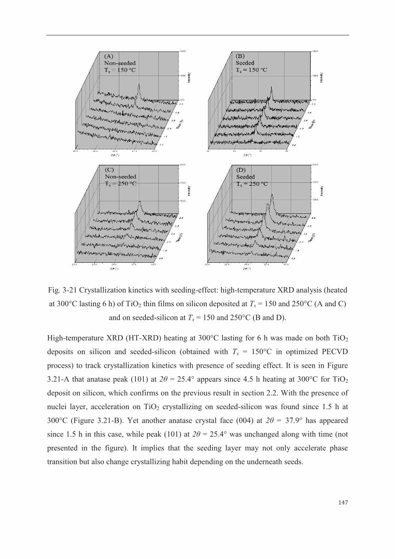
147
Fig. 3-21 Crystallization kinetics with seeding-effect: high-temperature XRD analysis (heated
at 300°C lasting 6 h) of TiO2 thin films on silicon deposited at Ts = 150 and 250°C (A and C)
and on seeded-silicon at Ts = 150 and 250°C (B and D).
High-temperature XRD (HT-XRD) heating at 300°C lasting for 6 h was made on both TiO2
deposits on silicon and seeded-silicon (obtained with Ts = 150°C in optimized PECVD
process) to track crystallization kinetics with presence of seeding effect. It is seen in Figure
3.21-A that anatase peak (101) at 2θ = 25.4° appears since 4.5 h heating at 300°C for TiO2
deposit on silicon, which confirms on the previous result in section 2.2. With the presence of
nuclei layer, acceleration on TiO2 crystallizing on seeded-silicon was found since 1.5 h at
300°C (Figure 3.21-B). Yet another anatase crystal face (004) at 2θ = 37.9° has appeared
since 1.5 h in this case, while peak (101) at 2θ = 25.4° was unchanged along with time (not
presented in the figure). It implies that the seeding layer may not only accelerate phase
transition but also change crystallizing habit depending on the underneath seeds.

148
In addition, higher PECVD substrate temperature (Ts = 250°C) has been operated for TiO2
deposition on seeded-silicon as well. It is more likely that stronger seeding activity could
occur at higher surface temperature. High-temperature XRD operated at 300°C for 6h has also
been made on the two samples (Ts = 250°C) as shown in Figure 3.21-C and D. Appearance of
both XRD peaks (101) at 2θ = 25.4° and (004) at 2θ = 37.9° has been observed on TiO2
deposits on silicon and seeded-silicon when Ts = 250°C. Yet only peak (101) is presented in
the figure for showing the evolution kinetics. TiO2 crystallization was accelerated from 3.5 to
1.5 h at 300°C due to seeding nuclei when Ts = 250°C in PECVD process. On the other
hand, Ts = 250°C enables saving 1 h of crystallization of TiO2 on silicon post-annealing at
300°C in comparison to that of Ts = 150°C in PECVD process.
As a conclusion, as-deposit TiO2 film on silicon (Ts = 150°C) has been crystallized into
anatase phase by post-annealing either at 400°C without staying or at 300°C with more than
4.5 h staying. Crystallization of TiO2 film on silicon can be saved by 1 h post-heating at
300°C when Ts has been increased to 250°C in PECVD process. Moreover, seeding nuclei
present on silicon surface accelerates phase transition to 1.5 h by post-heating at 300°C no
matter Ts = 150 or 250°C in PECVD procedure. Above all, concerning fully degree of
crystallization and removal of organic residues in the film the optimized post-thermal
treatment has been decided as 400°C for 3 hours for fabrication of photocatalytic membrane.
3 Structural properties of the optimal TiO2 thin film
Microstructure of supported TiO2 thin film and crystal size in the annealed-film was
characterized by SEM and XRD respectively. Photo-induced surface wettability of TiO2
surface was examined with water contact angle measurement. Band gap energy (Eg) of TiO2
thin film (deposited on glass in this case) was obtained from optical measurement. Porosity
and refractive index of the synthesis thin film have been studied with XRR and ellipsometry
spectroscopy analysis.
3.1 Morphology, crystal structure and photo-induced hydrophilicity
Microstructure of both amorphous and anatase TiO2 thin films was investigated in SEM with
their images presented in Figure 3-22. No structural damage due to post-annealing was found
and the anatase film maintained the porous micro-columnar morphology by comparing

149
as-deposited and post-annealed samples. Yet the anatase surface shows slight integration
effect after being heated at 400°C as presented in the surface image of Figure 3-22 (right).
Some tiny gaps on surface is observed for the annealed thin film maybe due to
dehydroxylation, release of organic residues and crystallization by heating.
Fig. 3-22 SEM images on the optimal TiO2 amorphous (left) and anatase (right) thin film on
silicon substrate.
FTIR spectra of the optimal amorphous and anatase TiO2 thin films are compared in Figure
3-23. Reduction absorbance of O-H stretching band for anatase film should be caused by
water evaporation and remove of organic residues due to post-annealing treatment at 400°C.
Characteristic shoulder peak at 700 cm-1 is observed for both amorphous and anatase phases,
whereas, a sharp peak at 450 cm-1 is only clearly witnessed for the anatase film. [198]
In addition, the chemical elements existing in the as-deposit thin film were analyzed by EDX
as the spectrum presented in Figure 3-24. Silicon has strong signal since the X-ray penetrate
the thin film and then to the silicon substrate. Carbon is detected in the film due to entrapped
organic residues from the precursor. And the atom ratio between titanium and oxygen is
found roughly as 1:2.5 before post-annealing.
Surface Surface
Cross-section (amorphous) Cross-section (anatase)
1.20 um1.20 um
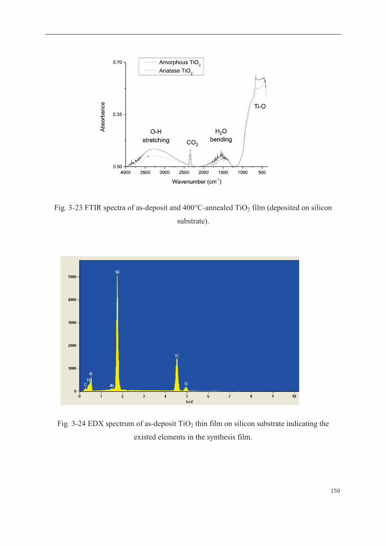
150
Fig. 3-23 FTIR spectra of as-deposit and 400°C-annealed TiO2 film (deposited on silicon
substrate).
Fig. 3-24 EDX spectrum of as-deposit TiO2 thin film on silicon substrate indicating the
existed elements in the synthesis film.
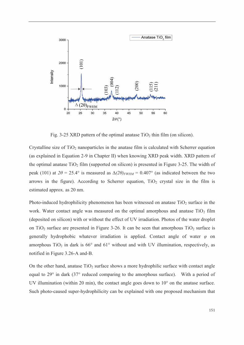
151
Fig. 3-25 XRD pattern of the optimal anatase TiO2 thin film (on silicon).
Crystalline size of TiO2 nanoparticles in the anatase film is calculated with Scherrer equation
(as explained in Equation 2-9 in Chapter II) when knowing XRD peak width. XRD pattern of
the optimal anatase TiO2 film (supported on silicon) is presented in Figure 3-25. The width of
peak (101) at 2θ = 25.4° is measured as ∆(2θ)FWHM = 0.407° (as indicated between the two
arrows in the figure). According to Scherrer equation, TiO2 crystal size in the film is
estimated approx. as 20 nm.
Photo-induced hydrophilicity phenomenon has been witnessed on anatase TiO2 surface in the
work. Water contact angle was measured on the optimal amorphous and anatase TiO2 film
(deposited on silicon) with or without the effect of UV irradiation. Photos of the water droplet
on TiO2 surface are presented in Figure 3-26. It can be seen that amorphous TiO2 surface is
generally hydrophobic whatever irradiation is applied. Contact angle of water φ on
amorphous TiO2 in dark is 66° and 61° without and with UV illumination, respectively, as
notified in Figure 3.26-A and-B.
On the other hand, anatase TiO2 surface shows a more hydrophilic surface with contact angle
equal to 29° in dark (37° reduced comparing to the amorphous surface). With a period of
UV illumination (within 20 min), the contact angle goes down to 10° on the anatase surface.
Such photo-caused super-hydrophilicity can be explained with one proposed mechanism that

152
oxygen vacancy in anatase surface is generated under UV source and it can be replaced by
hydroxyl group from H2O and thus the surface becomes more hydrophilic. [40]
Fig. 3-26 Water contact angle (φ) on TiO2 amorphous (A), irradiated amorphous (B), anatase
(C) and irradiated anatase (D).
3.2 Band gap energy (Eg)
Band gap energy (Eg) is an important property of photocatalytic material relevant to
photoelectrical transition and catalytic efficiency. Eg is defined as the energy difference
between two electronic levels: valence band (VB) and conduction band (CB). Eg can be
calculated from the optical measurement based on the light-and-matter interaction. In the
work, UV/Vis spectroscopy and ellipsometry spectroscopy have been carried out to study Eg
of the synthetic TiO2 thin films on substrate.
3.2.1 UV/Vis spectroscopy analysis on Eg
For UV/Vis absorbance analysis, TiO2 was synthesized on quartz substrate with the optimized
PECVD conditions as listed in Table 3-7. Samples Q1, Q2 and Q3 of TiO2 films with
different thickness have been deposited on the transparent substrate within deposition
duration as 7, 15 and 20 minutes in order to study TiO2 thickness effect on light transportation
through the film.

153
Table 3-7 PECVD conditions for preparing TiO2 samples Q1, Q2 and Q3 (on quartz).
Sample No.
Deposition duration
(min)
Partial pressure PAr+TTIP (mbar)
Partial pressure PO2
(mbar)
RF power
(W)
Plasma distance dp
(cm)
Substrate temp. Ts
(°C)
Q1 7 0.225 0.17 50 3 150
Q2 15 0.225 0.17 50 3 150
Q3 20 0.225 0.17 50 3 150
Mass of the glass substrate m1 (before PECVD process) and mass of TiO2-deposited glass m2
(after PECVD process) were measured in thermal mass balance respectively, in which the
temperature was controlled so that humilidity was kept in the same level relevant to water
absorbed on TiO2 surface. Consequently, mass of the as-deposit TiO2 film m3 could be known
by deducting m2 with m1. TiO2 mass per unit surface for sample Q1, Q2 and Q3 was obtained
by dividing m3 with glass surface area. Results are presented in Table 3-8. Thickness of TiO2
film (also given in the table) was theoretically obtained with knowing deposition rate and
deposition duration.
Table 3-8 Mass and thickness of TiO2 thin film deposited on quartz for samples Q1, Q2 and
Q3.
Sample No. a Mass of as-deposit TiO2 film
(amorphous)
b Thickness of TiO2 film
(amorphous and anatase)
Q1 0.6 g m-2 0.5 μm
Q2 3.0 g m-2 1.0 μm
Q3 4.0 g m-2 1.3 μm
a Mass of as-deposit TiO2 film : experimental values obtained from thermal-controlled balance and b
Thickness of TiO2 film: theoretical values calculated by multiplying the average deposition rate (R = 65 nm min-1) and the deposition duration (t = 7, 15 and 20 min).

154
Lambert-Beer law describes light-matter interaction when the light is passing through the
matter. In principle, more intensity of light can be absorbed with larger amount of molecules
in the film and there can be up-limit thickness that light can pass through. Absorbance spectra
of amorphous and anatase films are presented below.
250 300 350 400 450 500
0.0
0.3
0.6
0.9
Ab
so
rba
nce
Wavelength (nm)
Amorphous TiO2 (mass < 1 g/m
2)
Amorphous TiO2 (mass ~ 3 g/m
2)
Amorphous TiO2 (mass ~ 4 g/m
2)
Quartz support
Fig. 3-27 Light absorbance of as-deposit amorphous TiO2 films deposited on quartz.
250 300 350 400 450 500
0.0
0.3
0.6
0.9
Ab
so
rba
nce
Wavelength (nm)
Anatase TiO2 (thick < 0.5 mm)
Anatase TiO2 (thick ~ 1.0 mm)
Anatase TiO2 (thick ~ 1.5 mm)
Quartz support
Fig. 3-28 Light absorbance of 400°C-annealed anatase TiO2 films deposited on quartz.
Light absorbance of bared quartz and TiO2-deposited quartz was analyzed in UV
spectroscopy in the range 250 – 500 nm; spectra are given in Figure 3-27. Maximum

155
absorbance intensity the cut-off edge approx. wavelength 350 nm is found as 0.4, 0.65 and 0.7
for 7, 15 and 20-min deposited samples Q1, Q2 and Q3 (with deposited TiO2 mass per unit
surface ca. 0.6, 3.0 and 4.0 g m-2) respectively.
Q1, Q2 and Q3 samples were then annealed at 400°C and the anatase phase was form. Since
the mass of the anatase film could be different from the as-deposit form due to removal of
organic residues (as known from the previous TGA thermal analysis), theoretical thickness
values (multiplying average deposition rate and deposition duration) are indicated hereby.
Relevant UV spectra of the anatase Q1, Q2 and Q3 samples are plotted in Figure 3-28. Very
similarly, the intensity of absorbance is proportional to the anatase film thickness. Slight
change of absorption cutting-off edge has been caused after crystallization as seen in the
figure.
Fig. 3-29 Absorbance of light by sample Q3 of TiO2 film on quartz both in amorphous and
anatase phase.
Sample Q3 (20-minute deposit) absorbs the largest energy of incident light (in UV band λ <
350 nm) in comparison to the other samples Q1 and Q2. UV spectra of sample Q3 of both
amorphous and anatase phases are compared in Figure 3-29. It is found for sample Q3 that the
cut-off absorbance wavelength (λ) is 350 nm for amorphous and 365 nm for anatase by fitting
in the cut-off region. Fitting curve (in red) and absorbance λ value is illustrated for the anatase
TiO2 film in the figure.
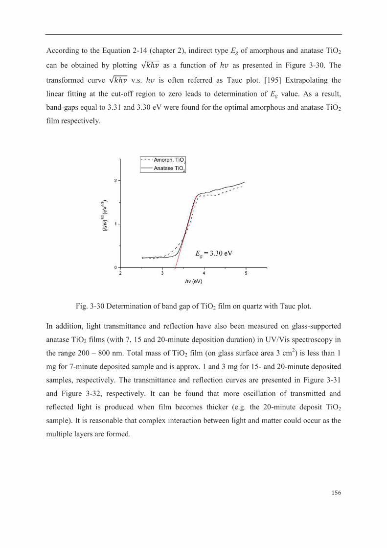
156
According to the Equation 2-14 (chapter 2), indirect type Eg of amorphous and anatase TiO2
can be obtained by plotting ¢J$2 as a function of $2 as presented in Figure 3-30. The
transformed curve ¢J$2 v.s. $2 is often referred as Tauc plot. [195] Extrapolating the
linear fitting at the cut-off region to zero leads to determination of Eg value. As a result,
band-gaps equal to 3.31 and 3.30 eV were found for the optimal amorphous and anatase TiO2
film respectively.
Fig. 3-30 Determination of band gap of TiO2 film on quartz with Tauc plot.
In addition, light transmittance and reflection have also been measured on glass-supported
anatase TiO2 films (with 7, 15 and 20-minute deposition duration) in UV/Vis spectroscopy in
the range 200 – 800 nm. Total mass of TiO2 film (on glass surface area 3 cm2) is less than 1
mg for 7-minute deposited sample and is approx. 1 and 3 mg for 15- and 20-minute deposited
samples, respectively. The transmittance and reflection curves are presented in Figure 3-31
and Figure 3-32, respectively. It can be found that more oscillation of transmitted and
reflected light is produced when film becomes thicker (e.g. the 20-minute deposit TiO2
sample). It is reasonable that complex interaction between light and matter could occur as the
multiple layers are formed.

157
Fig. 3-31 Transmittance of light through glass-supported anatase TiO2 films of different
thickness (deposited with 7, 15 and 20 minutes).
Fig. 3-32 Reflection of light from glass-supported anatase TiO2 films of different thickness
(deposited with 7, 15 and 20 minutes).
3.2.2 Ellipsometry spectroscopy analysis on Eg
In ellipsometry spectroscopy analysis a light beam (ellipse with a ~ 10 mm and b ~ 3 mm) is
employed on the optimal anatase TiO2 film (on silicon). Polarization parameters (α and β) in
the reflected light from the film are measured and regressed with various possible models.
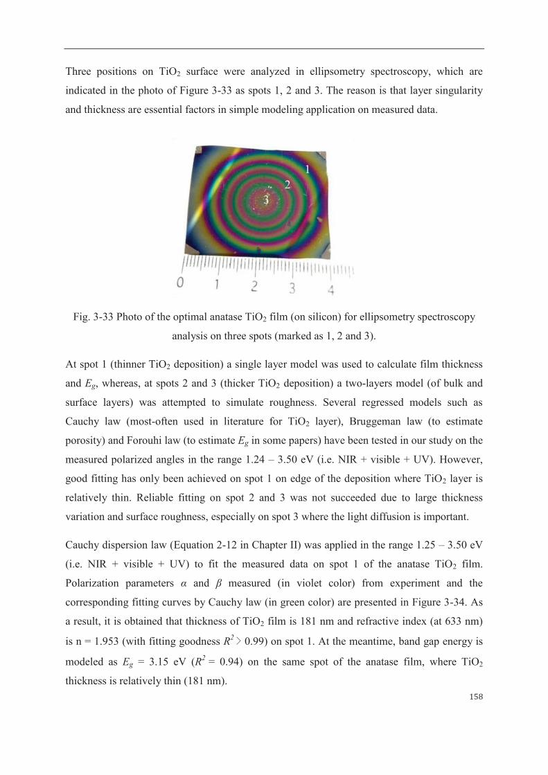
158
Three positions on TiO2 surface were analyzed in ellipsometry spectroscopy, which are
indicated in the photo of Figure 3-33 as spots 1, 2 and 3. The reason is that layer singularity
and thickness are essential factors in simple modeling application on measured data.
Fig. 3-33 Photo of the optimal anatase TiO2 film (on silicon) for ellipsometry spectroscopy
analysis on three spots (marked as 1, 2 and 3).
At spot 1 (thinner TiO2 deposition) a single layer model was used to calculate film thickness
and Eg, whereas, at spots 2 and 3 (thicker TiO2 deposition) a two-layers model (of bulk and
surface layers) was attempted to simulate roughness. Several regressed models such as
Cauchy law (most-often used in literature for TiO2 layer), Bruggeman law (to estimate
porosity) and Forouhi law (to estimate Eg in some papers) have been tested in our study on the
measured polarized angles in the range 1.24 – 3.50 eV (i.e. NIR + visible + UV). However,
good fitting has only been achieved on spot 1 on edge of the deposition where TiO2 layer is
relatively thin. Reliable fitting on spot 2 and 3 was not succeeded due to large thickness
variation and surface roughness, especially on spot 3 where the light diffusion is important.
Cauchy dispersion law (Equation 2-12 in Chapter II) was applied in the range 1.25 – 3.50 eV
(i.e. NIR + visible + UV) to fit the measured data on spot 1 of the anatase TiO2 film.
Polarization parameters α and β measured (in violet color) from experiment and the
corresponding fitting curves by Cauchy law (in green color) are presented in Figure 3-34. As
a result, it is obtained that thickness of TiO2 film is 181 nm and refractive index (at 633 nm)
is n = 1.953 (with fitting goodness R2 0.99) on spot 1. At the meantime, band gap energy is
modeled as Eg = 3.15 eV (R2 = 0.94) on the same spot of the anatase film, where TiO2
thickness is relatively thin (181 nm).

159
Fig. 3-34 Ellipsometry spectroscopy measurement curve (in violet) and the fitting curve (in
green) to calculate thickness and Eg of the anatase TiO2 film (on silicon).
3.3 Porosity
Porous column-like microstructure was discovered by SEM observation of PECVD TiO2 film
(session 3.1). However, the film porosity could not been directly measured with common
techniques including N2 adsorption/desorption method limited by the film’s thin thickness. In
the work, ellipsometry spectroscopy and X-ray reflectivity have been experimented to
investigate on the porosity in the deposited film.
Ellipsometry spectroscopy analysis on the anatase TiO2 thin film (at spot 1 as seen in the
photo of Figure 3-33) has been modeled with Bruggeman law (for mixture of TiO2 and void)
to estimate porosity. Polarization parameters (α and β) of the reflected light has been well
fitted in range 0.124 – 3.10 eV (i.e. NIR + visible) with the applied mathematics law. In a
result, the percentage of void volume in the film is found as v = 46 % (with fitting goodness
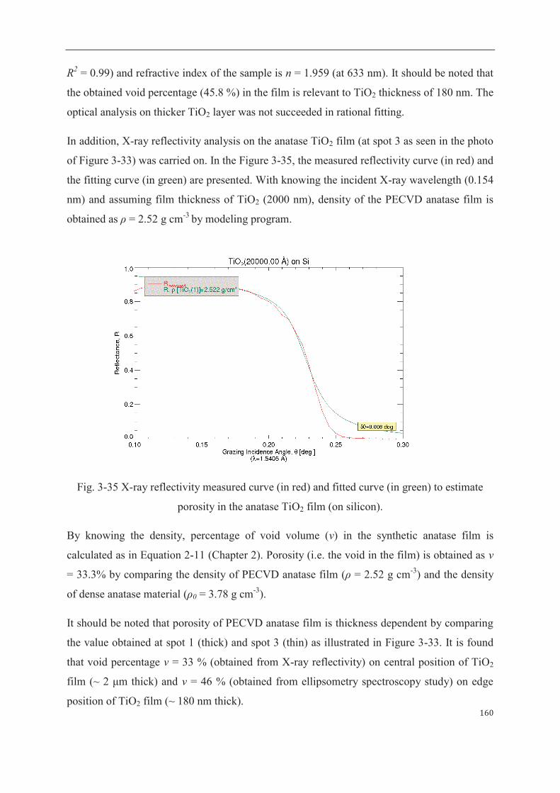
160
R2 = 0.99) and refractive index of the sample is n = 1.959 (at 633 nm). It should be noted that
the obtained void percentage (45.8 %) in the film is relevant to TiO2 thickness of 180 nm. The
optical analysis on thicker TiO2 layer was not succeeded in rational fitting.
In addition, X-ray reflectivity analysis on the anatase TiO2 film (at spot 3 as seen in the photo
of Figure 3-33) was carried on. In the Figure 3-35, the measured reflectivity curve (in red) and
the fitting curve (in green) are presented. With knowing the incident X-ray wavelength (0.154
nm) and assuming film thickness of TiO2 (2000 nm), density of the PECVD anatase film is
obtained as ρ = 2.52 g cm-3 by modeling program.
Fig. 3-35 X-ray reflectivity measured curve (in red) and fitted curve (in green) to estimate
porosity in the anatase TiO2 film (on silicon).
By knowing the density, percentage of void volume (v) in the synthetic anatase film is
calculated as in Equation 2-11 (Chapter 2). Porosity (i.e. the void in the film) is obtained as v
= 33.3% by comparing the density of PECVD anatase film (ρ = 2.52 g cm-3) and the density
of dense anatase material (ρ0 = 3.78 g cm-3).
It should be noted that porosity of PECVD anatase film is thickness dependent by comparing
the value obtained at spot 1 (thick) and spot 3 (thin) as illustrated in Figure 3-33. It is found
that void percentage v = 33 % (obtained from X-ray reflectivity) on central position of TiO2
film (~ 2 μm thick) and v = 46 % (obtained from ellipsometry spectroscopy study) on edge
position of TiO2 film (~ 180 nm thick).

161
4. Conclusion
Chemical bonding in the deposited film (a few micrometers thick) was observed in FTIR
spectrum at characteristic at wavenumber 450 and 700 cm-1 for anatase TiO2 material; in
addition, existing chemical elements of Ti and O atoms were proved in EDX spectrum.
Micro-columnar structure and thickness of the film have been witnessed and measured in
SEM. Crystalline phase was determined as anatase for the 400°C-annealed thin film with
XRD analysis, with nanocrystal size ca. 20 nm according to XRD peak width. Apparent
density of the synthesis anatase TiO2 film was known as 2.52 g cm-3 from XRR measurement
and accordingly the porosity of film could be estimated as 33% by comparing it to dense
anatase material. Photo-induced wettability on anatase surface was proved with reduction of
water contact angle from 29° to 10° due UV exposure. Band gap energy (Eg) of the optimally
prepared anatase film was found at 3.30 eV base on optical absorbance measurement. The
studied physico-chemical properties of the optimal anatase TiO2 film (on dense support
including silicon and quartz) are summarized in Table 3-9. They could affect photocatalytic
activity and membrane permeability, which will be discussed in the following chapter.
Table 3-9 Summary on physico-chemical properties of optimal PECVD TiO2 deposit.
Physico-chemical properties PECVD TiO2 thin film
Crystalline phase Anatase
Morphology Micro-columnar
Mean thickness 1.3 – 3.8 μm
Crystallite size 20 nm
Band gap energy Eg 3.30 eV
Apparent density 2.52 g cm-3
Porosity (thickness dependent) 33.3 %
(1.5 μm thick)
Water contact angle 29° (in dark)
10° (with UV)

162
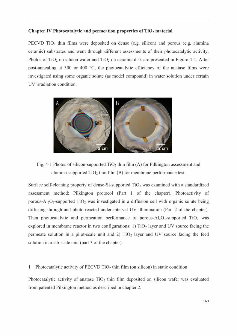
163
Chapter IV Photocatalytic and permeation properties of TiO2 material
PECVD TiO2 thin films were deposited on dense (e.g. silicon) and porous (e.g. alumina
ceramic) substrates and went through different assessments of their photocatalytic activity.
Photos of TiO2 on silicon wafer and TiO2 on ceramic disk are presented in Figure 4-1. After
post-annealing at 300 or 400 °C, the photocatalytic efficiency of the anatase films were
investigated using some organic solute (as model compound) in water solution under certain
UV irradiation condition.
Fig. 4-1 Photos of silicon-supported TiO2 thin film (A) for Pilkington assessment and
alumina-supported TiO2 thin film (B) for membrane performance test.
Surface self-cleaning property of dense-Si-supported TiO2 was examined with a standardized
assessment method: Pilkington protocol (Part 1 of the chapter). Photoactivity of
porous-Al2O3-supported TiO2 was investigated in a diffusion cell with organic solute being
diffusing through and photo-reacted under interval UV illumination (Part 2 of the chapter).
Then photocatalytic and permeation performance of porous-Al2O3-supported TiO2 was
explored in membrane reactor in two configurations: 1) TiO2 layer and UV source facing the
permeate solution in a pilot-scale unit and 2) TiO2 layer and UV source facing the feed
solution in a lab-scale unit (part 3 of the chapter).
1 Photocatalytic activity of PECVD TiO2 thin film (on silicon) in static condition
Photocatalytic activity of anatase TiO2 thin film deposited on silicon wafer was evaluated
from patented Pilkington method as described in chapter 2.

164
An example of time-resolved FTIR spectra of stearic acid adhered on anatase TiO2 surface
with UV irradiation is given in Figure 4-2. Photodegradation of stearic acid is witnessed as
the reduction of vibration band n(C-H) of stearic acid molecule (wavenumber from 2800 –
3000 cm-1) along with UV irradiating (35 W m-2, λ = 355 nm) duration equal to 0, 20, 40 and
60 minutes.
Fig. 4-2 Time-resolved FTIR spectra of photodegraded stearic acid caused by UV irradiated
TiO2 thin film deposited on silicon.
1.1 Effect of PECVD substrate temperature
Photodegradation rates of stearic acid related to anatase TiO2 layers deposited at different
substrate temperatures (Ts = 150 and 250 °C) are plotted along with irradiation time in Figure
4-3. It can be seen that all the anatase films (deposited at different Ts and then post-annealed
at the same Tp) have evident photocatalytic effectiveness on decomposing stearic acid within
80-min UV illumination. The used UV lamp had a polychromatic spectrum and an irradiance
of 35 W m-2 (measured with the UV radiometer at the bottom level of the Petri box). This UV
irradiation is corresponding to 1×10⁻⁴ mol of photon s-1 m-2. In the case of PECVD at Ts = 50
°C, RST caused by the anatase surface rises up to 70% at 80 min irradiation. In the case of
PECVD Ts caused by RST observed on the corresponding anatase thin films reaches 90 –
100% at the same irradiation time, which is representative of almost completely self-cleaning
surface. Less impurity (e.g. organic residues) entrapped in TiO2 layer in PECVD process at
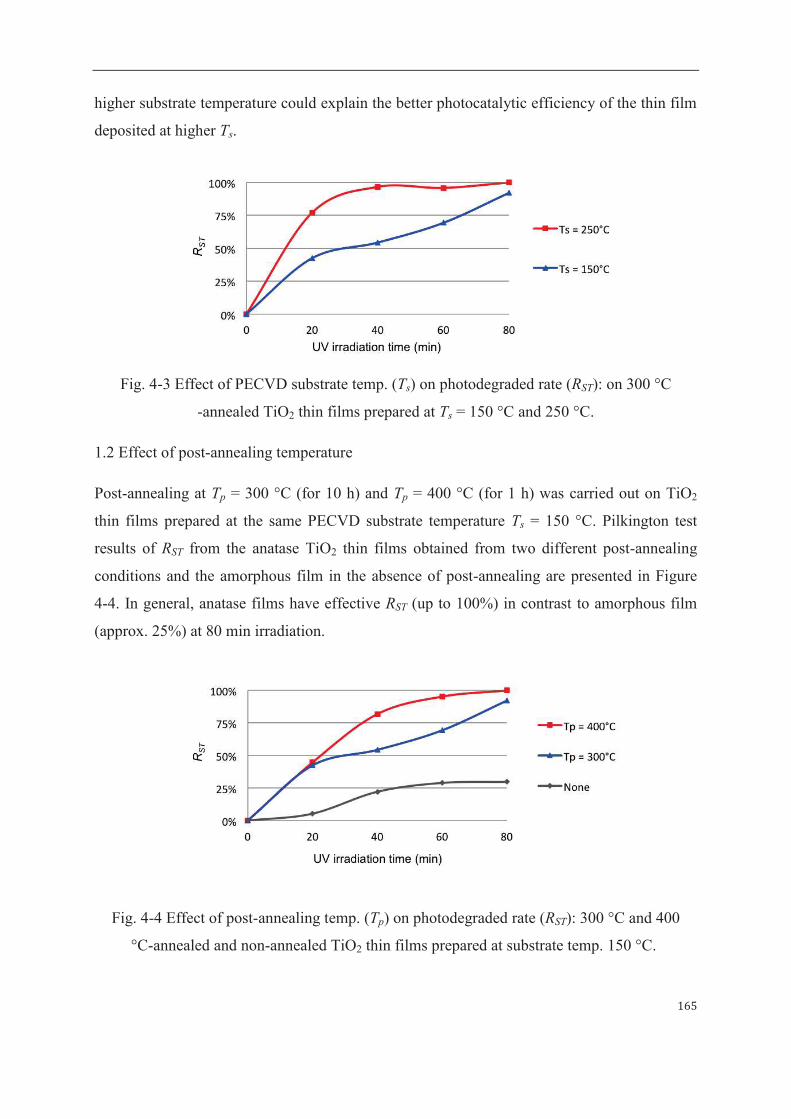
165
higher substrate temperature could explain the better photocatalytic efficiency of the thin film
deposited at higher Ts.
Fig. 4-3 Effect of PECVD substrate temp. (Ts) on photodegraded rate (RST): on 300 °C
-annealed TiO2 thin films prepared at Ts = 150 °C and 250 °C.
1.2 Effect of post-annealing temperature
Post-annealing at Tp = 300 °C (for 10 h) and Tp = 400 °C (for 1 h) was carried out on TiO2
thin films prepared at the same PECVD substrate temperature Ts = 150 °C. Pilkington test
results of RST from the anatase TiO2 thin films obtained from two different post-annealing
conditions and the amorphous film in the absence of post-annealing are presented in Figure
4-4. In general, anatase films have effective RST (up to 100%) in contrast to amorphous film
(approx. 25%) at 80 min irradiation.
Fig. 4-4 Effect of post-annealing temp. (Tp) on photodegraded rate (RST): 300 °C and 400
°C-annealed and non-annealed TiO2 thin films prepared at substrate temp. 150 °C.

166
Moreover, anatase film annealed at 400 °C (for 1 h) has improved photocatalytic efficiency
since 40 min irradiation in comparison to anatase film annealed at 300 °C (for 10 h). A
possible reason is that higher post-annealing temperature could have led to higher degree of
crystallinity in the film and to a more thorough removal of impurity.
At the mean time, uncoated silicon was examined with Pilkington test as a controlled
experiment, whose result of RST is compared to that of anatase-coated silicon (TiO2 deposited
at Ts = 150 °C and then post-annealed at Tp = 400 °C) as shown in Figure 4-5. Deduction of
stearic acid due to self-photolysis and/or evaporation caused by irradiation/thermal effect is
investigated in the controlled test on uncoated silicon.
Fig. 4-5 Self-cleaning surface on anatase-coated silicon (complete removal of stearic acid) in
contrast to the controlled experiment on the non-coated silicon.
Figure 4-5 shows that no significant degradation is observed on the uncoated substrate after
100 min of UV irradiation, whereas degradation is complete after 80 min for the
anatase-coated silicon wafer and 50 min are required to reach a degradation rate of 90%. Very
similar MB photodegradation rates are reported in the literature whatever the type (purely
ceramic or mixed with polymer, doped or not) and geometry (film, wire, tube, fiber etc.) of
titania membrane may be. [31, 126, 127, 199-201] The specific power of the UV device used,
35 W m-2, is close to that used in paper referenced [202] 32 W m-2, for the photocatalytic
characterization of titania layers prepared at high temperature by conventional CVD method.
For such dense layers (with stearic acid only adsorbed at the external surface), a degradation
rate of 90% was observed after a time of UV irradiation ranging from 4 to 28 min as a
function of the deposition conditions [202]. In another paper from our group dedicated to
mesostructured anatase layers prepared by sol-gel route and exhibiting a very high

167
photocatalytic activity [119] the same degradation rate requires an irradiation time of 10 s but
with a 11 times larger irradiation power (380 W m-2).
2 Photocatalytic activity of PECVD TiO2 thin film (on alumina) in diffusion condition
In order to characterize the photocatalytic activity of anatase-coated ceramics in diffusion
conditions, methylene blue (MB) as model compound in aqueous solution was studied in a
lab-scale diffusion cell. UV/Vis absorbance spectrum of MB in water was measured and a
maximum absorbance was found at λ = 665 nm as shown in Figure 4-6.
Fig. 4-6 UV/Vis absorbance spectrum of MB compound in water (C = 1×10⁻⁵ mol L-1).
Fig. 4-7 Calibration curve of absorbance of MB at λ = 665 nm (in water) versus
concentration.

168
A calibration curve was first established in order to determine the MB concentration in the
reception tank (in the range 10-6 – 10-5 mol L-1). The measured absorbance value of MB at λ =
665 nm was plotted as a function of C = 2×10⁻⁶, 4×10⁻⁶, 6×10⁻⁶, 8×10⁻⁶ and 1×10⁻⁵ mol L-1 as
presented in Figure 4-7. A linear fitting is acquired as calibration curve y = 61455x (R2 =
0.998), where y is absorbance at λ = 665 nm and x is concentration. Accordingly,
concentration of MB in the reception tank from the diffusion experiment is calculated from
the measured absorbance values.
The diffusion test described in chapter 2 was first implemented using a filter disk (from
Millipore: diameter 30 mm, thickness 0.41 mm and mean pore size 2.3 μm) as a reference
separator between the feed tank (filled with MB solution of C0 = 1×10⁻⁴ mol L-1) and
reception tank (filled with initially pure water). The amount of diffused MB per unit area (mol
m-2) was measured by the concentration in the reception tank versus diffusing time as
presented in Figure 4-8. The flux (J) is known from the slope of linear fitting on diffusivity
curve as J = 2.35×10⁻⁸ mol m-2 s-1. Diffusion coefficient (Di) of MB in water was calculated Di
= (J × d)/C0, where d is the thickness of separator (d = 0.41 mm) and C0 is the initial
concentration. Consequently, we have Di = 9.64×10⁻¹¹ m2 s-1 for MB molecules in pure water
in the case of initial feed C0 =1×10⁻⁴ mol L-1.
Fig. 4-8 Measurement on diffusion coefficient (Di) of MB compound in water.
2.1 Morphology and catalytic efficiency of TiO2-layer coating (M100)
Photodegradation tests in the diffusion cell were first performed on membrane M100.
Microstructure of M100 and its support are presented in SEM images of Figure 4-9. As mean

169
thickness of TiO2 layer is d layer μm (± 7%) and mean pore size of the support (in the top
layer) is Pr = 100 nm, then we have d ≥ 100 nm, thPr for this coating format for preparing
TiO2-Al2O3 composite membrane M100. Porosity of the columnar-like thin film is approx. 33%
(modeled from XRR) and TiO2 crystal dimension is approx. 20 nm (known from XRD).
Fig. 4-9 SEM images of membrane M100 (C and D) and the support (A and B).
The amount of transported MB through M100 in the absence of UV irradiation along with 8 h
is plotted in Figure 4-10. Following, the diffusion test was carried on the same membrane
with interval UV irradiation each another hour. Three repetition “diffusion + irradiation” tests
were made and displayed as 1st, 2nd and 3rd test in Figure 4-10.
Except the periods of alternated UV irradiation, MB concentration in the reception tank
versus time increases in agreement with Fick’s law. Moreover, it could be proved that the
mass balance in solution (feed and reception) is correctly respected, thanks to the initial
saturation of the membranes surface. During the irradiation times, a decrease of MB
concentration is observed in the reception tank. In some cases, the final concentration at the
end of the irradiation period is lower than the initial concentration at the beginning of the
previous period with UV. This result indicates that the destroyed amount of MB is larger than
that crossing the membranes by diffusion. From the change of slope corresponding to the UV
irradiation periods, it is possible to evaluate dMB, the quantity of destroyed MB per unit time
and per unit membrane surface area. [14]
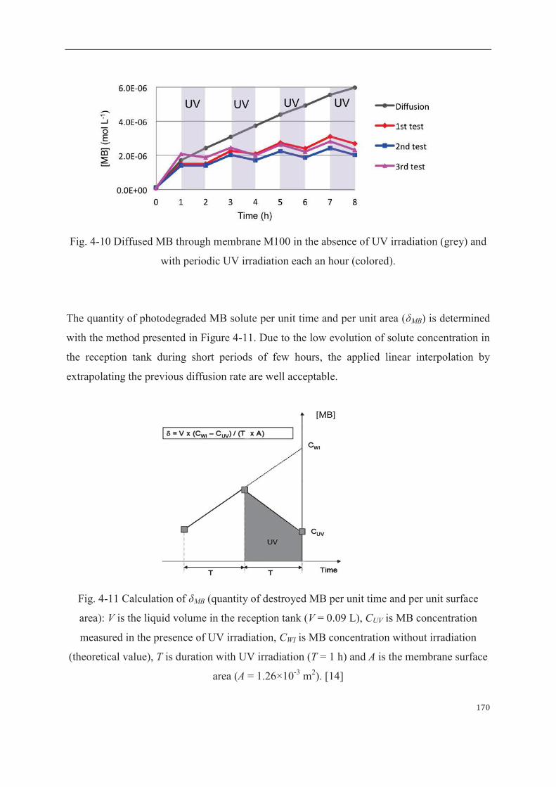
170
Fig. 4-10 Diffused MB through membrane M100 in the absence of UV irradiation (grey) and
with periodic UV irradiation each an hour (colored).
The quantity of photodegraded MB solute per unit time and per unit area (δMB) is determined
with the method presented in Figure 4-11. Due to the low evolution of solute concentration in
the reception tank during short periods of few hours, the applied linear interpolation by
extrapolating the previous diffusion rate are well acceptable.
Fig. 4-11 Calculation of δMB (quantity of destroyed MB per unit time and per unit surface
area): V is the liquid volume in the reception tank (V = 0.09 L), CUV is MB concentration
measured in the presence of UV irradiation, CWI is MB concentration without irradiation
(theoretical value), T is duration with UV irradiation (T = 1 h) and A is the membrane surface
area (A = 1.26×10⁻³ m2). [14]

171
Table 4-1 Values of δMB (quantity of photodegraded MB solute per unit time and per unit
membrane area) related to membrane M100 (TiO2-layer coating).
Time (h) δMB (mol/m2 s)
1st test 2nd test 3rd test
1 - UV off - - -
2 - UV on 1.99 × 10⁻⁸ 1.85 × 10⁻⁸ 3.21 × 10⁻⁸
3 - UV off - - -
4 - UV on 1.34 × 10⁻⁸ 1.40 × 10⁻⁸ 1.48 × 10⁻⁸
5 - UV off - - -
6 - UV on 1.43 × 10⁻⁸ 1.28 × 10⁻⁸ 1.52 × 10⁻⁸
7 - UV off - - -
8 - UV on 1.67 × 10⁻⁸ 1.37 × 10⁻⁸ 1.56 × 10⁻⁸
Average 1.61 × 10⁻⁸ 1.48 × 10⁻⁸ 1.94 × 10⁻⁸
As a result, δMB is calculated in the presence of UV irradiation (50 W m-2, 355 nm) and the
results from the three repetition tests are listed in Table 4-1. An average photodegradation
capacity is found in the magnitude of δMB = 2 × 10⁻⁸ mol m-1 s for TiO2-layer coating
membrane M100.
Similar degradation test was performed using ceramic support alone in order to prove the
absence of autophotolysis contribution. By comparing the evolutions of permeated
concentration through uncoated ceramic and TiO2-coated ceramic (M100) under periodic UV
irradiation as shown in Figure 4-12, there is no self-photolysis effect observed due to the
applied UV lamp. It is also found that the diffusion rate through the support differs that
through M100, which could be explained specific sorption and/or interaction of Al2O3-MB
and TiO2-MB. Surface hydrophilicity of Al2O3 and TiO2 could also be taken into account for
inorganic-organic interaction in aqueous circumstance.

172
Fig. 4-12 “Diffusion + irradiation” tests on membrane M100 and the support alone proving
the absence of self-photolysis.
2.2 Morphology and catalytic efficiency of TiO2-skin coating (M800)
TiO2-skin coating on alumina support (of top-layer pore size Pr = 800 nm) was achieved by
shortening PECVD duration. To obtain TiO2 coverage but without pore blockage on the
support, deposition durations of 3, 5, 7 and 10 min were respectively experimented in PECVD
process. SEM surface investigation are exhibited in Figure 4-13: inadequate TiO2 coverage is
observed for 3 and 5-min deposition (A and B); a properly covered surface with TiO2 is seen
on 7-min deposition (C) and excessive coverage is found on 10-min deposition (D).
Theoretical thickness of TiO2 coverage can be calculated with knowing the average
deposition rate as 65 nm min-1 with the optimized PECVD operating conditions.
Eventually, 7 min was determined in PECVD process to prepare membrane M800 with
TiO2-skin coating (theoretical thickness ~ 450 nm). SEM images of the membrane M800 and
the alumina support are presented in Figure 4-14.

173
Fig. 4-13 SEM surface images of TiO2 skin-covering on ceramic with variant PECVD
deposition duration: (A) 3 min, (B) 5 min, (C) 7 min and (D) 10 min.
Fig. 4-14 SEM images of membrane M800 (C and D) and the support (A and B).

174
MB in aqueous solution transported through the TiO2-skin coating membrane M800 was
measured as in the method described in previous section in the absence of UV irradiation
(increased MB concentration in reception tank due to concentration gradient) and in the
presence of periodic UV irradiation every another hour (change of MB concentration in
reception tank due to competition between diffusion and photodegradation rates). Results of
the diffusion test and repeated tests on “diffusion + irradiation are summarized in Figure 4-15.
Fig. 4-15 Diffused MB through membrane M800 in absence of UV irradiation (grey) and with
periodic UV irradiation each one hour (colored).
Quantity of photodegraded MB solute per unit time and per unit surface area (δMB) is
calculated with the same method previously explained. Averaged δMB values of of TiO2-skin
coated M800 membrane in the presence of periodic UV irradiation (50 W m-2, 355 nm) are
listed in Table 4-2. The result of average photodegrading capcity of membrane M800 is close
to 1×10⁻⁸ mol m-2 s-1.

175
Table 4-2 Values of δ (the quantity of photodegraded MB solute per unit time and per unit
membrane area) caused by membrane M800 (TiO2-skin coating).
Time (h) δMB (mol/m2 s)
1st test 2nd test 3rd test
1 - UV off - - -
2 - UV on 1.38 × 10⁻⁸ 3.28 × 10⁻⁸ 8.80 × 10⁻⁹
3 - UV off - - -
4 - UV on 6.33 × 10⁻⁹ 5.04 × 10⁻⁹ 4.22 × 10⁻⁹
5 - UV off - - -
6 - UV on 1.10 × 10⁻⁸ 6.57 × 10⁻⁹ 5.04 × 10⁻⁹
7 - UV off - - -
8 - UV on 9.45 × 10⁻⁹ 5.04 × 10⁻⁹ 4.93 × 10⁻⁹
Average 1.01 × 10⁻⁸ 1.24 × 10⁻⁸ 5.75 × 10⁻⁹
At the mean time, the same photodegradation test was made on the support of M800 in
diffusion conditions with the same UV operation. As shown in Figure 4-16, self-photolysis
effect is excluded on the relevant support alone.
Fig. 4-16 “Diffusion + irradiation” tests on membrane M800 and its support proving the
absence of self-photolysis.
In a summary, average values of dMB over three cycles under UV source (50 W m-2, 355 nm)
are 2×10⁻⁸ mol m-2 s-1 and 1×10⁻⁸ mol m-2 s-2 for membrane M100 and M800 respectively.

176
These values are in the same order of magnitude as those previously measured for titania
membranes prepared by sol-gel route in our group [14] or for Ag-titania-polymer composite
membranes in a very recent paper. [203] Moreover, these values are two orders of magnitude
higher than those measured for ceramic supports alone (2.4×10⁻¹⁰ mol s−1 m−2 and 3.6×10⁻¹⁰
mol s−1 m−2 for supports with 100 nm pore size and 800 nm pore size respectively), which
proves that supports do not contribute to the photodegradation.
3 Photocatalytic activity of PECVD TiO2-based membrane in dynamic condition
By applying pressure in the membrane process, catalytic performance of TiO2-based
membrane has been investigated in dynamic condition in two different membranes reactors:
one is placing photoactive TiO2 surface in contact with permeate solution (pilot-scale unit)
and the other is with feed solution (lab-scale unit).
3.1 Configuration with photoactive TiO2 layer toward the feed (pilot-scale unit)
As described in chapter 2, pure water permeance through TiO2-Al2O3 composite membranes
was first measured. The water permeance was determined from the volume flux of water
(Jwater) versus the transmembrane pressure (DP) as presented in Figure 4-17 and Figure 4-18
for membrane M100 and M800 respectively. For each membrane type, more than three
duplicated membranes were prepared and examined in water permeation test. In general,
reproducible permeating performance was observed.
Fig. 4-17 Water flux through three duplicated M100 membranes (with TiO2-layer coating).
0,0
0,3
0,5
0,8
1,0
0 0,25 0,5 0,75 1 1,25
J wa
ter
(L m
-2 s
-1)
ΔP (bar)
M100-1
M100-2
M100-3
Support

177
Fig. 4-18 Water flux through three duplicated M800 membranes (with TiO2-skin covering).
Water permeance was measured as 0.38 L m-2 s-1 bar-1 (i.e. 1368 L m-2 h-1 bar-1) and 1.89 L m-2
s-1 bar-1 (i.e. 6804 L m-2 h-1 bar-1) for M100 and M800, respectively. Such values of water
permeance are among the highest reported in the literature for many kinds of titania
membranes. [127, 199-201, 204] A higher flow permeance of the M800 is obtained due to
higher mean pore size of the support and absence of a denser top layer. Indeed, as shown
previously, in the case of M100, the anatase film is in the form of conform top layer, whereas
in the case of M800, the anatase material is not an entire layer but a skin-coverage.
In the case of M100, the water permeance is slightly higher than that of the support alone
(0.41 L s-1 m-2 bar-1) maybe due to hydrophilicity of the additional anatase layer. In the case
of M800, the water permeance is almost twice higher than that of the support alone (1.11 L s-1
m-2 bar-1), certainly due to the pronounced hydrophilic nature of the anatase material (water
contact angle equal to 29° as measured for a plasma film deposited on silicon wafer in a
previous paper by our group. [31] As a comparison, the water contact angle of a naturally
oxidized silicon is in the range 60-70°. [205]) On the other hand, PECVD coating could have
plasma etching effect on the substrate that increases a general porosity in the substrate. For
instance the porosity was discovered as 44.5% and 36.8% for M100 and its support with
mercury porosimetry method. In both cases, the permeation ability of membranes has been
clearly demonstrated.
0,0
1,0
2,0
3,0
4,0
0 0,25 0,5 0,75 1 1,25
J wa
ter
(L m
-2 s
-1)
ΔP (bar)
M800-1
M800-2
M800-3
Support

178
Table 4-3 Calculating the expected photodegradation ratio of MB (C/C0) according to the
measured δMB (from diffusion condition) and water flux J (at ΔP = 0.25 bar).
Membr.
type
δMB
(mol m-2 s-1)
ΔP
(bar)
Jwater
(L m-2 s-1)
C = δMB/Jwater
(mol L-1)
C0 in pilot
(mol L-1)
Expected
C/C0
M100-1 2 × 10⁻⁸ 0.25 0.15 1.33 × 10⁻⁷ 2.50 × 10⁻⁷ 53%
M100-2 2 × 10⁻⁸ 0.25 0.18 1.11 × 10⁻⁷ 2.50 × 10⁻⁷ 44%
M800-1 1 × 10⁻⁸ 0.25 0.9 1.25 × 10⁻⁸ 1.25 × 10⁻⁷ 10%
M800-2 1 × 10⁻⁸ 0.25 0.8 1.11 × 10⁻⁸ 1.25 × 10⁻⁷ 9%
As UV lamp being switched on, concentration in the permeation flow (Cpilot) was analyzed
each 5 min in 60-min operation. The experimental values of photodegradation rate RMB
measured on M100 and M800 membranes are presented in Figure 4-19.
Fig. 4-19 Measured photodegradation RMB on membranes M100 (duplicated) and M800
(duplicated) in the pilot-scale unit with constant UV irradiation (50 W/m2, 355 nm).
The first 20-min RMB was not constant due to the geometry of pilot cell that permeate
compartment has 50 mL remaining solution (without being photodegraded) to run out of the
unit. After consumption of the remained permeation solution (in 20 min), constant reduced
concentrations were found in the permeating flow because of photocatalysis process with
continuous UV illumination. Membrane M100 performed about 5 times higher photocatalytic

179
efficiency than that of M800, which could be caused by slower transmembrane flowing speed
and larger dMB of M100. It was observed that approx. 50% of MB molecules in water has been
degraded by M100 membranes from feed concentration 3.2 × 10⁻⁷ mol L-1 at transmembrane
pressure 0.25 bar. Whereas for M800 membrane, it was found that approx. 10% of MB
molecules was destroyed from the feed of concentration 1.25 × 10⁻⁷ mol L-1 at the same
pressure.
As displayed in Figure 4-20 and Figure 4-21, the experimental results of photodegrading
capacity of M100 and M800 respectively are in very good accordance with expected values
(Table 4-3). It proves the absence of defects on membranes and pilot-scale unit. Moreover,
reproducible performance was maintained on duplicate membranes of each coating format
under the same pilot operation.
Fig. 4-20 Expected and experimental RMB values on duplicate membrane M100-1 and M100-2
with UV irradiation (50 W m-2, 355 nm).

180
Fig. 4-21 Expected and experimental RMB values on duplicate membrane M800-1 and M800-2
with UV irradiation (50 W m-2, 355 nm).
3.2 Configuration with photoactive TiO2 layer in contact with feed (lab-scale unit)
As described in chapter 2, model compound acid orange 7 (AO7) and phenol have been used
as due compounds in the lab-scale membrane reactor configured with photo-active TiO2 layer
to the feed. UV lamp either of low intensity 4 W (at λ = 254 nm or λ = 365 nm) or of high
intensity 500 W (UVA emission from 360 nm) has been employed as the irradiation source to
study their effect on membrane’s photocatalytic efficiency.
3.2.1 Acid orange 7 as degraded model compound
UV absorbance spectrum from wavelength 200 – 500 nm of prepared AO7 solution is
presented in Figure 4-22, where a maximum absorbance wavelength was found at 485 nm.
Following, the calibration curve of AO7 absorbance at λ = 485 nm versus concentration of
AO7 solution is plotted in Figure 4-23.
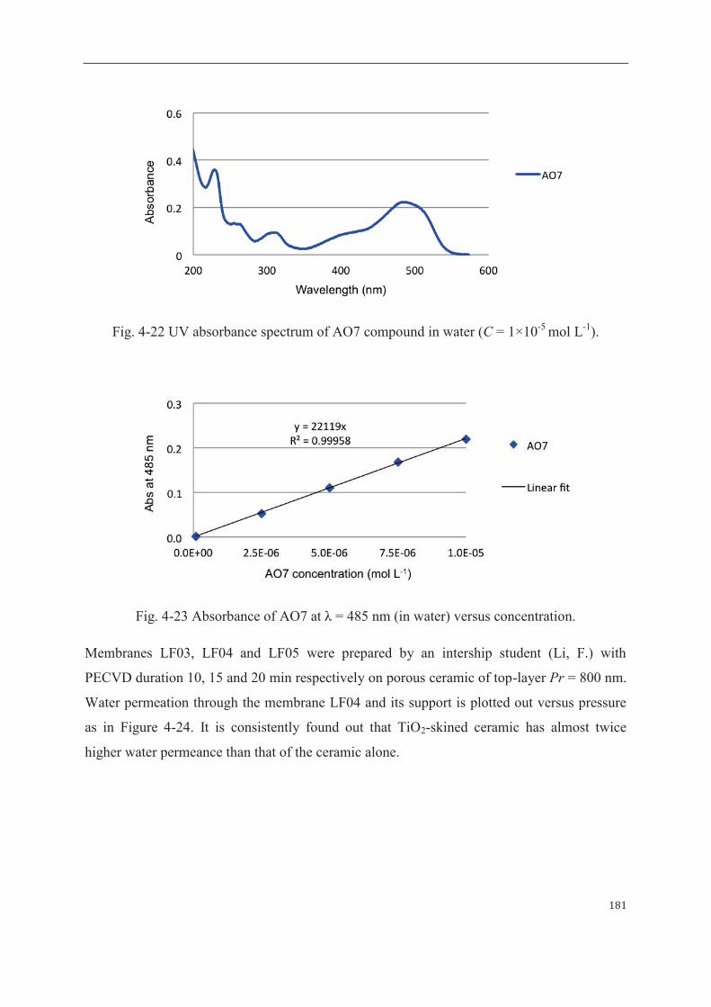
181
Fig. 4-22 UV absorbance spectrum of AO7 compound in water (C = 1×10⁻⁵ mol L-1).
Fig. 4-23 Absorbance of AO7 at λ = 485 nm (in water) versus concentration.
Membranes LF03, LF04 and LF05 were prepared by an intership student (Li, F.) with
PECVD duration 10, 15 and 20 min respectively on porous ceramic of top-layer Pr = 800 nm.
Water permeation through the membrane LF04 and its support is plotted out versus pressure
as in Figure 4-24. It is consistently found out that TiO2-skined ceramic has almost twice
higher water permeance than that of the ceramic alone.
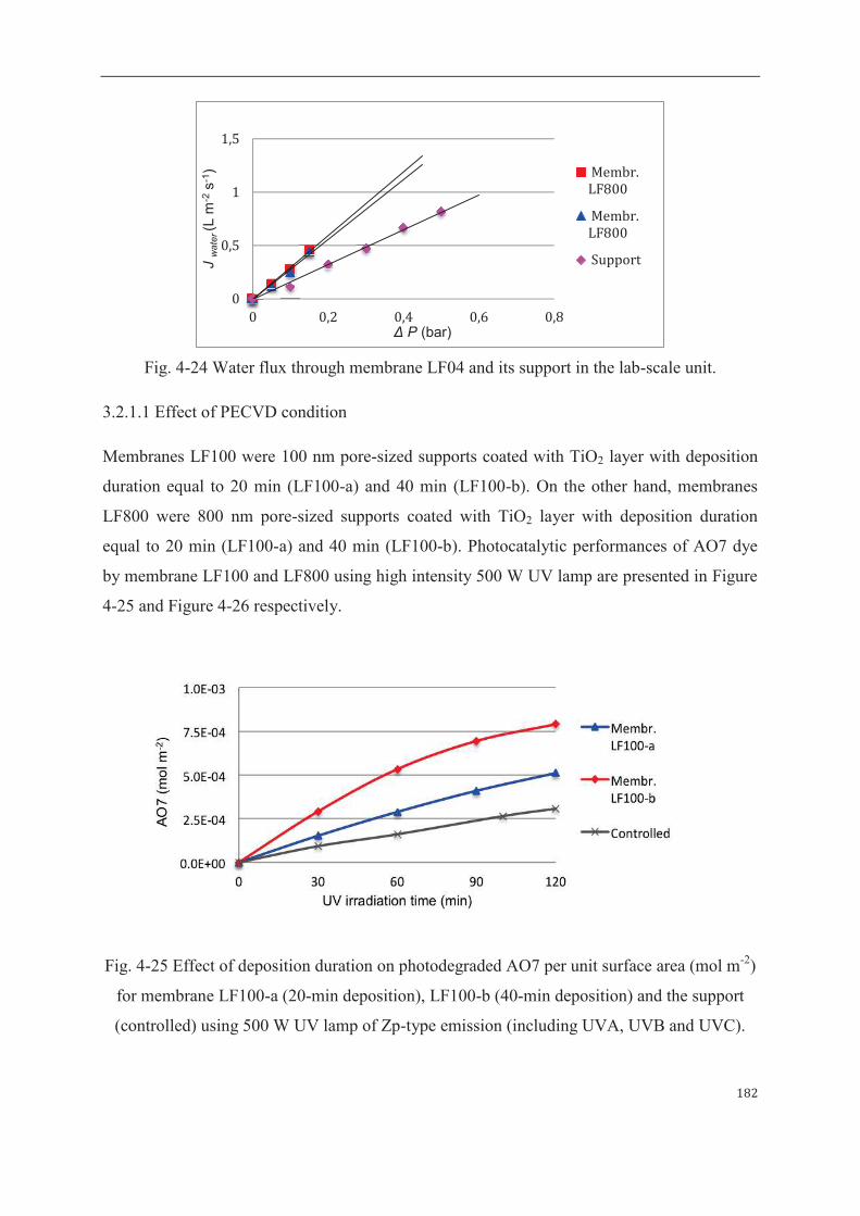
182
Fig. 4-24 Water flux through membrane LF04 and its support in the lab-scale unit.
3.2.1.1 Effect of PECVD condition
Membranes LF100 were 100 nm pore-sized supports coated with TiO2 layer with deposition
duration equal to 20 min (LF100-a) and 40 min (LF100-b). On the other hand, membranes
LF800 were 800 nm pore-sized supports coated with TiO2 layer with deposition duration
equal to 20 min (LF100-a) and 40 min (LF100-b). Photocatalytic performances of AO7 dye
by membrane LF100 and LF800 using high intensity 500 W UV lamp are presented in Figure
4-25 and Figure 4-26 respectively.
Fig. 4-25 Effect of deposition duration on photodegraded AO7 per unit surface area (mol m-2)
for membrane LF100-a (20-min deposition), LF100-b (40-min deposition) and the support
(controlled) using 500 W UV lamp of Zp-type emission (including UVA, UVB and UVC).
0
0,5
1
1,5
0 0,2 0,4 0,6 0,8
J w
ate
r (L
m-2
s-1
)
Δ P (bar)
Membr.
LF800
Membr.
LF800
Support

183
Fig. 4-26 Effect of deposition duration on photodegraded AO7 per unit surface area (mol m-2)
for membrane LF800-a (20-min deposition), LF800-b (40-min deposition) and the support
(controlled) using 500 W UV lamp of Zp-type emission (including UVA, UVB and UVC).
Thicker TiO2 layer (made with longer deposition duration) has improved the
photodegradation rate of AO7 in the first cast of membrane LF100 (as seen in Figure 4-25),
however such effect is not observed in the second case of membrane LF800 (as seen in Figure
4-26).
3.2.1.2 Effect of UV irradiation
UV lamp devices of high intensity (500 W) and low intensity (4 W) have been experimented
and studied with their effect on photodegradation efficiency. The 500W UV lamp has option
of Zp-type emission including UVA, UVB and UVC (from 180 nm to visible range) and of
Zs-type emission including UVA (from 360 nm) . The 4 W UV lamp has alternative emitting
wavelength either 365 nm or 264 nm. The lab-scale unit was operated with membrane LF800
and its support (as controlled experiment) using AO7 dye solution of initial concentration
1×10⁻⁵ mol L-1 and volume 60 mL. Circulation speed 30 ml min-1 and transmembrane
pressure 0.1 bar have been maitained in the membrane process.
Both lamp devices were tested on membrane LF800 for degrading aqueous AO7 dye, whose
results are presented in Figure 4-27 and Figure 4-28 respectively. As seen in Figure 4-27, 500
W lamp illuminated LF800 membranes shows almost complete decomposition of AO7 (up to
95%, i.e. degraded solute per unit area equal to 5.0 × 10⁻⁴ mol m-2) within 2 h with both
emission types of Zp and Zs. The self-photolysis effect (as the controlled) with the support

184
alone presents almost triple degradation degree (ca, 17%) under broader irradiation spectrum
(Zp type) than that under the only UVA spectrum (Zs type).
Fig. 4-27 Effect of irradiation spectrum on on photodegraded AO7 per unit surface area (mol
m-2) for membrane LF800 and the support (controlled) using 500 W UV lamp with alternative
emission of Zp-type (UVA, UVB and UVC) and Zs-type (UVA).
Fig. 4-28 Effect of irradiation wavelength on photodegraded AO7 per surface area (mol m-2)
for membrane LF800 and its support alone (as controlled) using 4 W powered-UV lamp with
alternative emission λ = 365 nm or λ = 254 nm.
By replacing the 500 W UV lamp with the 4 W one (Figure 4-28), self-photolysis has been
significantly reduced as less than 5% of AO7 was degraded within 2 h in the absence of
photocatalytic layer. On the same membrane LF800, UV emission at λ = 365 nm caused a
slightly enhanced degradation rate 54% (i.e. destroyed AO7 per unit area as 2.5 × 10⁻⁵ mol
m-2) in contrast to emission at λ = 254 nm with degradation rate 45% (i.e. 2.0 × 10⁻⁵ mol m-2).

185
In a summary, photodegradation efficiency has been improved less than 10 times from 2.5 ×
10-5 mol/m2 (with 4 W UV irradiation) to 3.5 × 10⁻⁴ mol/m2 (with 500 W UV lamp) by
increasing more than 100 times of irradiation intensity. The 500 W lamp with Zs-type
emission (only UVA) could be the best option of the studied devices in terms of the fastest
photoreaction kinetics and a very low self-photolysis effect, yet the operation of this lamp
needs to be done with more cares due to peronsal protection from the high irradiation.
3.2.1.3 Effect of dynamic conditions in membrane process
Membrane LF05 was planted in the lab-scale membrane cell and the pressure-driven
membrane process was operated in the same way as mentioned previously in terms of AO7
feed solution and high-intensity UV Zs type emission (UVA from 360 nm). In many number
of successive photodegradation experiments, variant transmembrane pressure of 0.05, 0.10
and 0.15 bar and flowing speeds of 20, 30 and 40 mL/min were carried out in the membrane
process. Corresponding photodegradation rates of AO7 under the aspect dynamic conditions
were respectively recorded along with irradiation duration 2 h.
At a fixed flowing speed of 30 mL/min in the system, transmembrane pressures ΔP equal to
0.05, 0.10 and 0.15 bar resulted in generally similar catalytic effectiveness on membrane
LF05 as shown in Figure 4-29. At the end of 2.5 h irradiation, photodegradation rate reached
close to 85%, 85% and 90% at ΔP = 0.05, 0.10 and 0.15 bar, respectively. The reaction
efficiency is faster when applied pressure is higher as could been observed for the evolution
curve recorded at 0.15 bar. Moreover the amount of decomposed solute per unit membrane
area is 5.9 × 10⁻⁴ mol/m2 at the highest-pressure condition. It could be explained by Langmuir
model of adsorption that higher pressure (or concentration) leads to larger adsorbing capacity
before the saturation of monolayer sorption.

186
Fig. 4-29 Effect of transmembrane pressure (0.10 and 0.15 bar) on photodegraded AO7 per
unit surface area (mol m-2) for membrane LF800 with fixed circulation speed 30 ml min-1
under 500 W-powered UV Zs-type emission (UVA).
On the other hand, obtained photodegradation evolutions versus irradiation time were
measured at fixed ΔP = 0.10 bar with variant flowing speeds of 20, 30 and 40 mL min-1.
Results of photodegradation rates are displayed in Figure 4-30. Degraded rates of 90%, 86%
and 82% have been observed on the same membrane at 2-h irradiation with circulating speeds
of 20, 30 and 40 mL min-1 respectively. The slower feed flowing speed sweeping on
membrane surface has resulted in faster catalytic efficiency. Moreover, the amount of
decomposed aqueous AO7 per unit membrane area is 8 × 10⁻⁸ mol m-2 s-1 at the lowest
circulation speed. The contacting time between the solute and TiO2 active sites could be
maintaining longer when the horizontal flowing is slower. Close values of photodegradation
rate of AO7 (RAO7) as 90.2% and more than 90% within 2 h reaction time were found in the
individual work of Zhang et al. using TiO2 hollow fiber membrane [206] and Bai et al. using
SrTiO3/TiO2 fibers modified cellulose acetate membrane [207, 208]. In Zhang et al.’s work,
initial AO7 solution of volume 20 ml and concentration 20 mg L-1 (i.e. 5.7 × 10⁻⁵ mol L-1) was
used in the membrane process operating at transmembrane pressure 0.9 bar and circulation
speed 40 ml min-1 (with a relatively slow water flux through the membrane at 12.2 L m-2 h-1
comparing to our results). In Bai et al.’s work, initial concentration of AO7 solution 50 mg L-1
(i.e. 14.3× 10⁻⁵ mol L-1) and similarly slow water flux 10 L m-2 h-1 at 1.5 bar was maintained
during the tests. In addition, Mendret et al. used TiO2/Al2O3 composite membrane and found
an optimal pH = 4 for photodegrading aqueous AO7 with reaction rate as 15.6 μmol L-1 min-1,

187
whose membrane having permeability coefficient close to ours as high as 1200 L m-2 h-1 [209,
210].
Fig. 4-30 Effect of transmembrane pressure (0.10 and 0.15 bar) on photodegraded AO7 per
unit surface area (mol m-2) for membrane LF800 with fixed circulation speed 40 ml min-1
under 500 W-powered UV Zs-type emission (UVA).
3.2.2 Phenol as degraded model compound
Phenol (C6H6O) has been used as the dye compound for the characterization of membrane
M100, using a 4 W-powered UV irradiation at λ = 365 nm. Concentration of phenol in
aqueous solution was analyzed with HPLC-UV method. An example of HPLC-UV analysis
on phenol solution is given in Figure 4-31. Retention time of phenol in the applied HPLC
method was found at 4.7 min. Absorbance at wavelength 254 nm was measured at each
retention time and thus concentration of phenol solution was calculated from calibration
curve.
Adsorption of phenol on membrane M100 and the support along has been carried out at 37 °C.
The adsorbed phenol per unit volume within 100 min is presented in Figure 4-32. It is
consistently found that the porous support itself could have larger adsorbing capacity for
organic solute as the previous work on sorption of AO7 compound. As explained previously,
different wettability of alumina and anatase TiO2 surfaces.

188
Fig. 4-31 HPLC-UV analysis on phenol in aqueous solution.
Photodegradation experiment was carried out using phenol solution of initial concentration 1×
10-4 mol/L (10 times higher than the case of AO7 compound in previous work) and in the
volume 65 mL. Low intensity 4 W-powered lamp with emission at λ = 365 nm was applied as
the UV source in the test. The feed tank was maintained at 24 and 37 °C as the reaction
temperature, whose results on the amount of degraded phenol by the membrane M100 is
given in Figure 4-32. Transmembrane pressure was studied at 0.3, 0.5 and 0.7 bar at constant
circulation speed 40 mL min-1 with the corresponding degraded number of phenol is given in
Figure 4-33.
Fig. 4-32 Degraded phenol at different reaction temperature of 24 °C and 37 °C operated at
the same transmembrane pressure 0.7 bar.
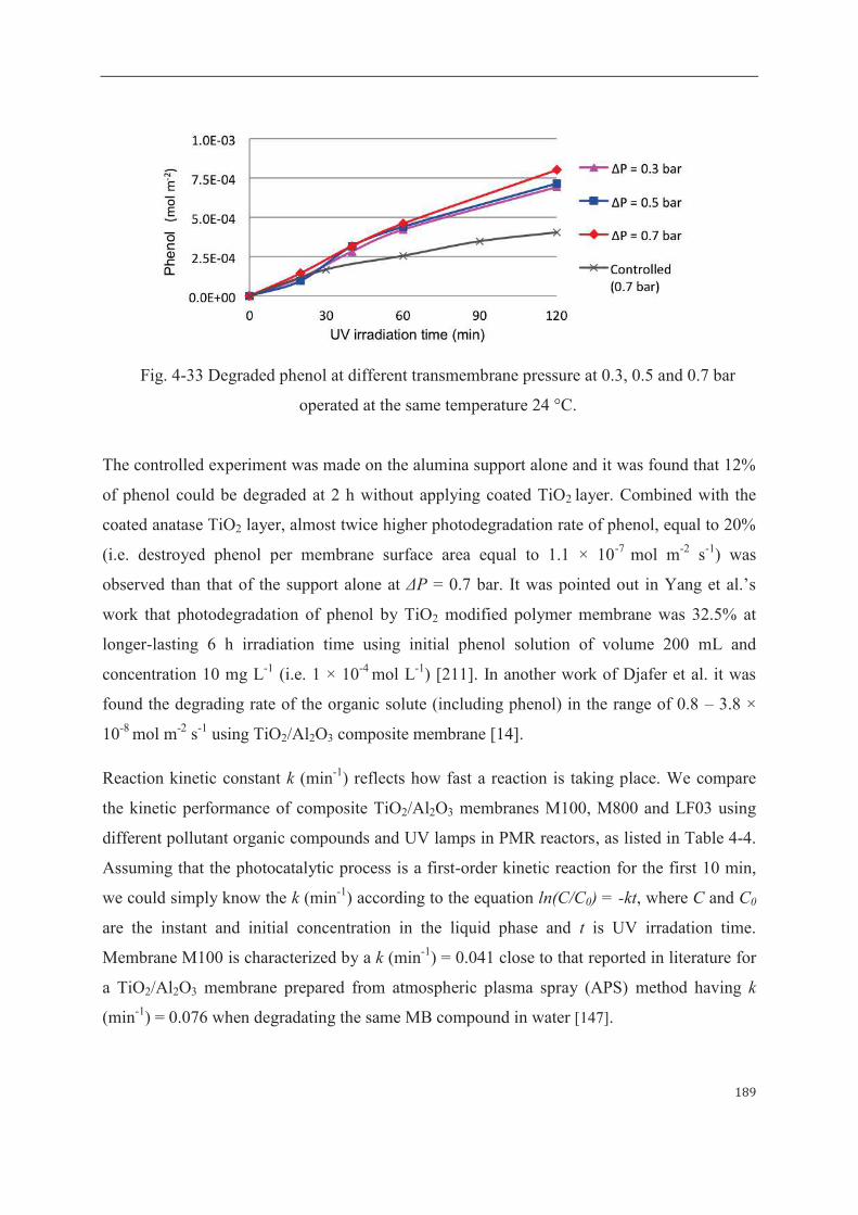
189
Fig. 4-33 Degraded phenol at different transmembrane pressure at 0.3, 0.5 and 0.7 bar
operated at the same temperature 24 °C.
The controlled experiment was made on the alumina support alone and it was found that 12%
of phenol could be degraded at 2 h without applying coated TiO2 layer. Combined with the
coated anatase TiO2 layer, almost twice higher photodegradation rate of phenol, equal to 20%
(i.e. destroyed phenol per membrane surface area equal to 1.1 × 10⁻⁷ mol m-2 s-1) was
observed than that of the support alone at ΔP = 0.7 bar. It was pointed out in Yang et al.’s
work that photodegradation of phenol by TiO2 modified polymer membrane was 32.5% at
longer-lasting 6 h irradiation time using initial phenol solution of volume 200 mL and
concentration 10 mg L-1 (i.e. 1 × 10⁻⁴ mol L-1) [211]. In another work of Djafer et al. it was
found the degrading rate of the organic solute (including phenol) in the range of 0.8 – 3.8 ×
10-8 mol m-2 s-1 using TiO2/Al2O3 composite membrane [14].
Reaction kinetic constant k (min-1) reflects how fast a reaction is taking place. We compare
the kinetic performance of composite TiO2/Al2O3 membranes M100, M800 and LF03 using
different pollutant organic compounds and UV lamps in PMR reactors, as listed in Table 4-4.
Assuming that the photocatalytic process is a first-order kinetic reaction for the first 10 min,
we could simply know the k (min-1) according to the equation ln(C/C0) = -kt, where C and C0
are the instant and initial concentration in the liquid phase and t is UV irradation time.
Membrane M100 is characterized by a k (min-1) = 0.041 close to that reported in literature for
a TiO2/Al2O3 membrane prepared from atmospheric plasma spray (APS) method having k
(min-1) = 0.076 when degradating the same MB compound in water [147].

190
Table 4-4 Photocatalytic reaction kinetic constant k (min-1) of composite TiO2/Al2O3
membranes prepared with PECVD method in this work. (MB: methylene blue and AO7: acid
orange 7)
Membrane Reaction kinetics
k (min-1)
Polluant compound in water
UV irradiation
M100 0.041 MB (3×10⁻⁷ mol L-1) 355 nm, 50 W m-2
M800 0.010 MB (1.25×10⁻⁷ mol L-1) 355 nm, 50 W m-2
LF03 0.017 AO7 (1×10⁻⁵mol L-1) 360 nm, 760 W m-2
LF03 0.007 AO7 (1×10⁻⁵mol L-1) 365 nm, 18 W m-2
M100 0.017 Phenol (1×10⁻⁴mol L-1) 365 nm, 18 W m-2
As a summary, lab-scale unit with membrane’s photoactive surface in contact with feed
solution and pilot-scale unit with the active surface in contact with permeate solution have
been both experimented. Degraded model compounds including MB, AO7 and phenol were
used to investigate photocatalytic performance of membrane M100 and membrane LF04.
Moreover, UV sources of options different intensity and emitting wavelengths were tested
their effect on photodegradation reaction. Further on, the dynamic conditions as
transmembrane pressure and circulation speed were examined in the testing membrane
process.
4 Modeling of sorption and photocatalyzed reaction process
4.1 Modeling of sorption experiments
To identify independently the sorption parameters of membrane the sorption experiments in
batch system has been carried out as described in chapter 2.
4.1.1 Mathematical descriptions

191
Two mathematical models have been developed. The first one is neglecting the effect of
diffusion in body of membrane the second one is taking the effect of diffusion into account.
These models have been used for evaluation of adsorption rate constants and sorption
capacities.
Adsorption model 1
This model is neglecting external and internal mass transfer and accounting the infinite
diffusion rate inside the membrane body (including the TiO2 layer and Al2O3 porous support).
Under these assumptions the concentration of i-th component in liquid phase inside of porous
structure of membrane is equal to the concentration in tank and no concentration gradient in
liquid phase is present.
The mass balance equation for i-th component in the tank can be written as:
where denotes the concentration of i-th component in tank, volume of tank ,
volume of membrane with support and τ time.
The mass balances for adsorption of i-th component in catalytic layer and support are given
by following Equation 4-2 and Equation 4-3.
The initial conditions are: , , .
Adsorption model 2
This model is neglecting external mass transfer and only the effect of diffusion in both
membrane layer and support is taken into account. The mass balance of i-th component in
tank under this assumption can be described by equation 4-4:
ic V MSV
0S
iq = 0M
iq = 0i ic c=
(4-1)
(4-2)
(4-3)
( ) ( )1 1M M S SM SiMS M ads S ads
M S M S
dcV V r r
d
d e d er r
t d d d d- -é ù
= - +ê ú+ +ë û
MMi
ads
dqr
dt=
SSi
ads
dqr
dt=

192
The mass balance equations in porous photo-active layer contain mass transport by diffusion
and adsorption on catalyst surface:
where is diffusion coefficient of component i and is assumed constant along all axial
coordinate x.
The mass balance equations in porous support is also accounting for mass transport by
diffusion and adsorption on membrane support surface
The initial, boundary and interfacial conditions are as follow:
iD
(4-4)
(4-5)
(4-6)
(4-7)
(4-8)
0 M S
M S
i i iM M Mi M S Si
x x
dc c cV A D A D
d x xd d
e et
= = +
¶ ¶= -
¶ ¶
( )2
2
1M MM Mi i
i M ads
M
c cD r
x
er
t e-¶ ¶
= -¶ ¶
MMi
ads
qr
t¶
=¶
( )2
2
1S SS Si i
i S ads
S
c cD r
x
er
t e-¶ ¶
= -¶ ¶
SSi
ads
qr
t¶
=¶
0 0 0 00 : , , ,M M S S M M S S
i i i i i i i ic c c c q q q qt < = = = =
0 :t ³ 0 : M
i ix c c= =
:M S
i iM M S
M S
i i
c cx
x x
c c
d e e¶ ¶
= =¶ ¶=
: S
M S i ix c cd d= + =
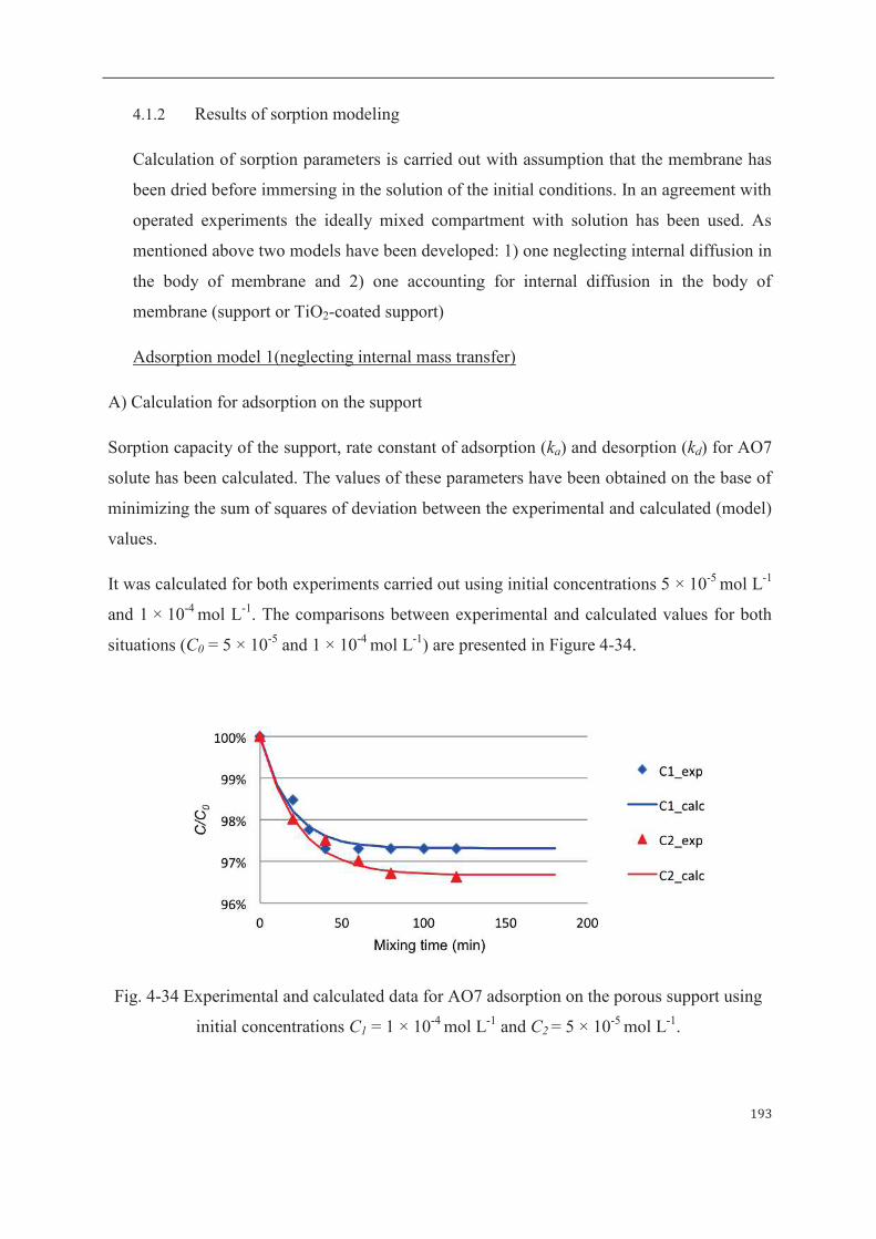
193
4.1.2 Results of sorption modeling
Calculation of sorption parameters is carried out with assumption that the membrane has
been dried before immersing in the solution of the initial conditions. In an agreement with
operated experiments the ideally mixed compartment with solution has been used. As
mentioned above two models have been developed: 1) one neglecting internal diffusion in
the body of membrane and 2) one accounting for internal diffusion in the body of
membrane (support or TiO2-coated support)
Adsorption model 1(neglecting internal mass transfer)
A) Calculation for adsorption on the support
Sorption capacity of the support, rate constant of adsorption (ka) and desorption (kd) for AO7
solute has been calculated. The values of these parameters have been obtained on the base of
minimizing the sum of squares of deviation between the experimental and calculated (model)
values.
It was calculated for both experiments carried out using initial concentrations 5 × 10⁻⁵ mol L-1
and 1 × 10⁻⁴ mol L-1. The comparisons between experimental and calculated values for both
situations (C0 = 5 × 10⁻⁵ and 1 × 10⁻⁴ mol L-1) are presented in Figure 4-34.
Fig. 4-34 Experimental and calculated data for AO7 adsorption on the porous support using
initial concentrations C1 = 1 × 10⁻⁴ mol L-1 and C2 = 5 × 10⁻⁵ mol L-1.

194
For all the continuous calculations on sorption (with effect of diffusion) and photodegradation
experiments, we have used the estimated constants (Qsat, ka, kd) obtained from the experiments
as explained in Figure 4-35.
Table 4-5 Optimized constants for sorption on the porous support.
Bared support
V (L) 0.005
ka (L mol-1 min-1) 219.12
kd (min-1) 3.2812 × 10⁻²
Qsat (mol L-1) 9.1576 × 10⁻⁵
DS (mm) 27
δS (mm) 1
VS (L) 3.722 × 10⁻⁴
C0 (mol L-1) 1 × 10⁻⁴ 5 × 10⁻⁵
Θeq 0.3939 0.2440
Ceq (mol L-1) 9.7315 × 10⁻⁵ 4.8337 × 10⁻⁵
Keq (L mol-1) 6.6782 × 10³
Parameters in the Table 4-5 such as Θeq, Ceq and Keq (Keq = ka/kd) indicate the equilibrium
surface coverage, equilibrium concentration of AO7 in solution and equilibrium constant of
sorption respectively. The constants ka, kd and Qsat in Table 4-5 are related with respect to the
volume of solid material.
The reaction rate in form relevant to volume:
By comparing it with eq for description of reversible adsorption in model above, we have the
reaction rate relevant to the weight of material:
(4-9)

195
By relating the Equations 4-9 and 4-10, we have:
We can find the relation between these constants as:
(4-12)
(4-13)
(4-14)
where is density of solid in support. The same approach can be used for TiO2 layer when
recalculating constant between different units.
Fig. 4-35 Time dependency of surface coverage (θ) of adsorbed AO7 on porous support using
initial concentrations C1 = 1 × 10⁻⁴ mol L-1 and C2 = 5 × 10⁻⁵ mol L-1.
Sr
(4-10)
(4-11)
( )* *
1 1[mol/weight of solid/min] 1 1
s ss S s S s S Si i
ads i ads i i iS S S S
ads ads
q qr k c k c
q K q K
é ù é ùæ ö= - - = - Q - Qê úç ÷ ê ú
è ø ë ûë û
( ) ( )*
1
1 11 1
S S
ads S
S SS s S S s S SA aads i i i i i iS S S
ads eq
r r
q kk c c
K K
r
r
=
é ùé ù- Q - Q = - Q - Qê úê ú
ê úë û ë û
**[ / / min]
S SS S SA aads aS
q kk L g q k
r= =
S S
eq adsK K=
**
[ / ][ / ]
[ / ]
SS A
S
q mol Lq mol g
g Lr=

196
B) Calculation for adsorption on TiO2-coated support
Comparing the adsorption results with barred support and TiO2-coated support it is evident
that during preparation of TiO2-coated support the structural changes resulting in change of
sorption properties of material take place. The sorption capacity of coated support is
substantially lower. The decrease in the sorption capacity could be the consequence of support
sintering process or/and partial covering of internal structure of support by deposited TiO2
which seems to adsorb notably lower amount of AO7. There was carried out adsorption
experiments with initial concentrations of AO7 solution 1 × 10⁻⁴ and 5 × 10⁻⁵ mol L-1. With
respect to the low adsorption capacity of TiO2-coated support the changes in concentration of
AO7 solution were close to the experimental error of measurement and cannot be used for
parameter estimation. The decrease of amount of used solution with respect to volume of
membrane could improve the sensitivity of experiment. But even decreasing the volume to
the minimal value possible (5 mL) did not lead to an improvement. There were no
independent data from adsorption measurements on TiO2 layer unaffected by the porous
support available therefor we have treated the TiO2-coated support as “mixed materials” and
we assumed mean values of adsorption related constants (Qsat, ka, kd) identical for both
materials.
The comparison of model and experimental data for LF100 membrane is shown on Figure
4-36. The model prediction is in good agreement with experimental data. The obtained
constants are summarized in Table 4-6.
Fig. 4-36 Experimental and calculated data for AO7 adsorption on TiO2-Al2O3 composite
membrane LF100 using initial concentrations C1 = 1 × 10⁻⁴ mol L-1.
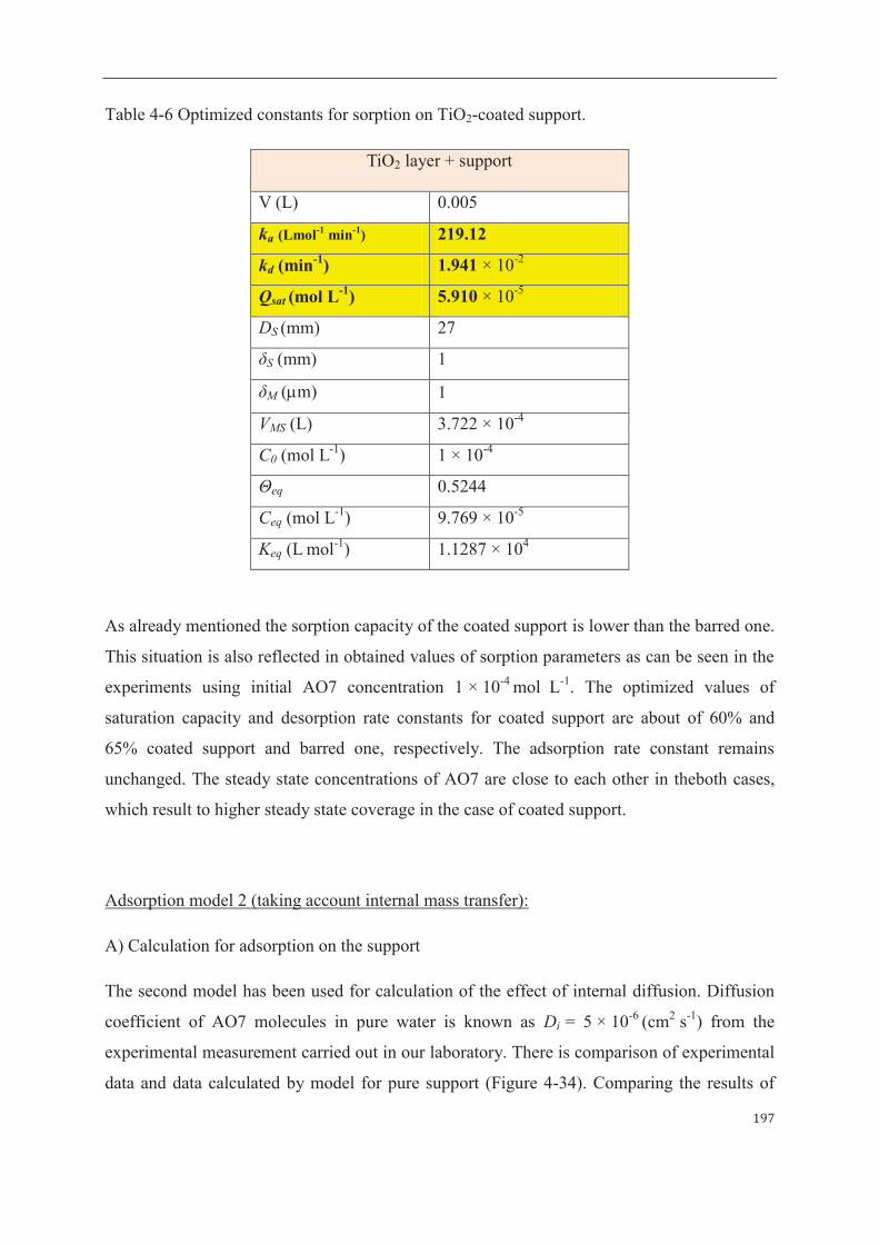
197
Table 4-6 Optimized constants for sorption on TiO2-coated support.
TiO2 layer + support
V (L) 0.005
ka (Lmol-1 min-1) 219.12
kd (min-1) 1.941 × 10⁻²
Qsat (mol L-1) 5.910 × 10⁻⁵
DS (mm) 27
δS (mm) 1
δM (mm) 1
VMS (L) 3.722 × 10⁻⁴
C0 (mol L-1) 1 × 10⁻⁴
Θeq 0.5244
Ceq (mol L-1) 9.769 × 10⁻⁵
Keq (L mol-1) 1.1287 × 10⁴
As already mentioned the sorption capacity of the coated support is lower than the barred one.
This situation is also reflected in obtained values of sorption parameters as can be seen in the
experiments using initial AO7 concentration 1 × 10⁻⁴ mol L-1. The optimized values of
saturation capacity and desorption rate constants for coated support are about of 60% and
65% coated support and barred one, respectively. The adsorption rate constant remains
unchanged. The steady state concentrations of AO7 are close to each other in theboth cases,
which result to higher steady state coverage in the case of coated support.
Adsorption model 2 (taking account internal mass transfer):
A) Calculation for adsorption on the support
The second model has been used for calculation of the effect of internal diffusion. Diffusion
coefficient of AO7 molecules in pure water is known as Di = 5 × 10⁻⁶ (cm2 s-1) from the
experimental measurement carried out in our laboratory. There is comparison of experimental
data and data calculated by model for pure support (Figure 4-34). Comparing the results of

198
model accounting diffusion in internal structure of membrane (Figure 4-37) with results of the
one neglecting this effect (Figure 4-34) there are almost negligible differences between the
values of calculated time concentration profiles in reservoir.
Fig 4-37 Experimental and calculated data of AO7 adsorption on the porous support by taking
account diffusion coefficient of AO7 as Di = 5 × 10⁻⁶ cm2 s-1 and using initial concentrations
C1 = 1 × 10⁻⁴ mol L-1and C2 = 1 × 10⁻⁵ mol L-1.
Using the mathematical model including the effect of diffusion the information about time
changes of concentration and surface coverage profiles inside the porous structure can be
obtained. The results of calculation of these profiles for experiment carried out with initial
concentration of AO7 C1 = 1 × 10⁻⁴ mol L-1 are presented in figures 4-38 and 4-39. The
adsorption reaction in the initial stage of experiment is relatively fast with respect to the
diffusion into the body of support and the concentration profile with minimum in centre of
support is formed (Figure 4-38) as shown for the times 7, 14 and 29 min, respectively. The
differences between concentration in the centre of support and at the boundaries of support
are decreasing with increasing time and diminish when the steady state is reached (Figure
4-38). The surface coverage profiles have also minimum in the centre of support body but it is
not pronounced as in the case of concentration in the liquid phase (Figure 4-39). The surface
coverage is increasing with time and after 50 min of experiment the differences in
concentration in the centre of support and at the boundaries is negligible.

199
Fig. 4-38 Dimensionless concentration profiles of AO7 in liquid phase inside the porous
structure of support as function of time. The symbol x denotes the dimensionless axial
coordinate inside support. (Barred support, initial concentrations of AO7 C0 = 1 × 10⁻⁴ mol
L-1, volume of AO7 solution 5 mL, diffusion coefficient of AO7 as Di = 5 × 10⁻⁶ cm2 s-1).
Fig. 4-39 Surface coverage (theta) profiles inside the porous structure of support as function
of time. The symbol x denotes the dimensionless axial coordinate inside support. (Barred
support, initial concentrations of AO7 C0 = 1 × 10⁻⁴ mol L-1, volume of AO7 solution 5 mL,
diffusion coefficient of AO7 as Di = 5 × 10⁻⁶ cm2 s-1).

200
B) Calculation for adsorption on TiO2-coated support
Calculation on the data was made by considering a combination of support + TiO2 layer with
the relevant constants obtained from the previous calculation for this material. The results of
these calculations are summarized on figures 4-40 and 4-41. The behaviour of concentration
and surface coverage profiles are analogous to the ones in case of barred support with the
exceptions that the higher surface coverage is reached at steady state and the maximal
difference between concentrations in the centre and at boundaries is lower for TiO2-coated
support. The difference between the concentrations in the centre and boundaries is related to
the ratio of adsorption rate and diffusion flux. When the rate of consumption of species by
adsorption is higher with respect to the diffusion flux the difference increases as for the case
of barred support.
Fig. 4-40 Dimensionless concentration profiles of AO7 in liquid phase inside the porous
structure of TiO2-coated support as function of time. The symbol x denotes the dimensionless
axial coordinate. (TiO2-coated support, initial concentrations of AO7 C0 = 1 × 10⁻⁴ mol L-1,
volume of AO7 solution 5 mL, diffusion coefficient of AO7 Di = 5 × 10⁻⁶ cm2 s-1).

201
Fig. 4-41 Surface coverage (theta) profiles in the porous structure of TiO2-coated support as
function of time. The symbol x denotes the dimensionless axial coordinate in support.
(TiO2-coated support, initial concentrations of AO7 C0 = 1 × 10⁻⁴ mol L-1, volume of AO7
solution 5 mL, diffusion coefficient of AO7 as Di = 5 × 10⁻⁶ cm2 s-1).
4.2 Modeling of photocatalytic experiments
General mathematical model has been developed taking into account experimental
arrangement described in Chapter II. The schematic drawing of modelled system is shown in
Figure 2-18 and Figure 2-24 of Chapter II.
4.2.1 Mathematical descriptions
The system consists of three mains parts 1) tubing, 2) tanks, and 3) photocatalytic cell with
membrane. Equations for the individual parts are developed separately. The complete model
comprises the equations for individual parts bounded through the boundary conditions. The
changes of the temperature through the effects of chemical reactions, sorption, light, mixing
etc. are neglected. The isothermal conditions are assumed in this study and the final model is
based on mass balances only.
4.2.1.1 Mass balance of tubing
The tubing has been separated into three sections as follows:

202
1) Feed tube – connection of feed tank and photocatalytic reactor
2) Retentate tube – the outlet of retentate from photocatalytic reactor
3) Permeate tube – the outlet of permeate from photocatalytic cell
Dynamic model of isothermal plug flow reactor with axial dispersion and non-compressible
fluid has been used to describe the individual tubes. Bulk homogeneous reactions in tube and
surface reactions on the wall of tube are taken into account to the general form of equation.
The surface reactions can be used to describe sorption of component on tube wall. This
equation can be written as:
(4-15)
Where denotes concentration of component I, time, the axial coordinate,
axial dispersion coefficient, velocity, stoichiometric coefficient in bulk reaction,
reaction rate of bulk reaction, tube radius, stoichiometric coefficient in surface reaction,
and reaction rate of surface reaction on the tube wall, respectively.
As has been verified experimentally, the reactions in the bulk phase and the adsorption on
tube surface can be neglected. The equation can be rewritten in form:
(4-16)
The initial and boundary conditions are:
( ), , ,
2i b si iax i ij b j ij s j
j jt
vcc cD r r
z z z rn n
t
¶æ ö¶ ¶¶= - + +ç ÷¶ ¶ ¶ ¶è ø
å å
ic t zaxD
v b
ijn br
trs
ijn
sr
( ),
ii iax i
vcc cD
z z zt
¶æ ö¶ ¶¶= -ç ÷¶ ¶ ¶ ¶è ø
00 : ( )i iz c c t= =
,: 0it ax i
cz L D
z
¶= =
¶

203
where is the length of tube and is initial concentration. The boundary conditions for
individual tube are set appropriately in dependency of arrangement of experimental set-up and
they are defined with details in summary table of model equations.
4.2.1.2 Mass balance of tanks
Feed tank (constant contribution) and permeate tank (depending on permeate fully or partially
recycling back to the feed) are present in the lab-scale and pilot-scale photocatalytic
membrane reactor (PMR) units.
1) Mass balance of feed tank
General mass balance equation of feed tank is also accounting homogeneous bulk reactions
and the dynamic model of ideally mixed semi-batch tank reactor is used. To describe the
different arrangement of experiments (with recycling permeate to the feed tank and the one
with fully or partially separated permeate) the factor is introduce to the equation. This
factor defines the ratio of permeate recycled back to the feed tank. Then we have
for the case where no permeate recycling and where all permeate recycling back to
the feed tank. The mass balance equation of i-th component is given as:
(4-17)
where the is the volume of feed tank, are the molar concentrations of
component I in feed tank, permeate and retentate respectively. The symbols , ,
denote the volumetric flows of retentate, permeate, and feed respectively. The reaction term
can be neglected because no reactions have been identified during blank
experiments. Thus the final equation is given as:
(4-18)
The total mass balance of feed tank is described by following equation:
tL 0ic
sf
0fs =
1fs =
FTV , ,FT P R
i i ic c c
FT FT FT
ij j
j
V rnå

204
where , , are the densities of liquid in retentate, feed tank and permeate,
respectively. Aqueous solution of low concentration of organic solute has been used in all
experiments and isothermal conditions were assumed so that the change of densities with
change of concentration of dye can be neglected and the Equation 4-19 can be rewritten to use
volumetric flows only:
The flow of permeate ( ) can be calculated based on water permeation measurements and
is defined by equation below:
where is water permeance, , the pressure in retentate and permeate compartment
respectively, and identifies the cross-membrane pressure drop. The feed flow is defined
by pump delivery.
The initial conditions for Equations 4-8 and 4-9 are defined by initial concentration of i-th
component and amount of solution in feed tank as:
2) Mass balance of permeate tank
As for the derivation of mass balance equations for permeate tank, similar assumptions as
given in the feed tank have been also used hereby. The mass balance of i-th component is then
given in Equation 4-22 and total mass balance in Equation 4-23.
Rr FTr Pr
wp Rp Pp
pD
(4-19)
(4-20)
(4-21)
(4-22)
0 00 : ,FT FT FT FT
i iV V c ct = = =
205
4.2.1.3 Mass balance of photocatalytic cell
For the purpose of mathematical modeling, the photocatalytic cell has been divided into three
sections:
1) Retentate compartment
2) Permeate compartment
3) Membrane (composite of the support + TiO2 layer)
which are to be discussed one to one as following:
1) Mass balance of retentate compartment
The retentate compartment has been simulated as dynamic continuous stirred tank reactor to
which the feed is input from feed tank and the retentate is removed. Part of the mixture also
permeates through the membrane to the permeate side and it is controlled by setting cross
membrane pressure drop. In the general form of the applied modeling it is assumed that the
reactions can take place in homogenous phase. TiO2 catalyst is assumed to be on the top of
support and it is oriented in direction toward the retentate compartment. The external mass
transfer resistance has been neglected and the near membrane surface concentration is equal
to the bulk concentration in retentate compartment. The mass balance equation of i-th
component is then given in Equation 4-24:
(4-23)
The initial conditions are described as:
(4-24)
0 00 : ,PT PT PT PT
i iV V c ct = = =

206
where introduces the concentration of i-th component in retentate compartment, the
volume of retentate compartment, the membrane area, the membrane porosity,
effective axial dispersion coefficient of i-th component in membrane, concentration of
i-th component in membrane and term the contribution of bulk reactions in
retentate compartment respectively.
Performed experimental test showed that the contribution of bulk reactions in retentate
compartment can be neglected. Under this assumption the Equation 4-24 can be written in
modified form of Equation 4-25.
The total mass balance can be written as:
The initial conditions of Equation 4-15 are defined as:
2) Mass balance of permeate compartment
The derivation of mass balance equation for permeate compartment is based on similar
assumptions as in the case of retentate side and the final equation can be given in form:
where denotes volume of permeate compartment, the concentration of i-th
component in permeate compartment, the porosity of support layer, effective axial
dispersion coefficient in support layer, the concentration of i-th component in fluid
(liquid) phase in support, the thickness of photocatalytic layer, thickness of
support. The initial conditions are given as:
RC
icRCV
MA Me MiD
M
ic
RC RC
ij j
j
rnå
PCV PC
ic
se SiD
S
ic
Md Sd
(4-25)
(4-26)
(4-27)
00 : RC RC
i ic ct = =

207
3) Mass balance in photocatalytic membrane
The mass balance equations in porous photo-active layer contain mass transport by
convection, dispersion as well as the adsorption and reaction on catalyst surface:
where denotes membrane porosity, the molar concentration of i-th component in
fluid (liquid) phase, the local interstitial fluid velocity in membrane porous space,
the effective dispersion coefficient of i-th component, the density of membrane solids
catalyst, rate of adsorption, concentration of adsorbed species i in solid catalyst,
rate of photocatalytic decomposition of i-th component.
Rate of reversible adsorption of i-th component in photocatalytic membrane is given by:
where stands for the rate constant of adsorption in membrane, the equilibrium
constant of adsorption in membrane, concentration of adsorption sites in membrane.
Rate of photocatalytic reaction (irreversible) is described:
where is concentration of holes generated by photon flux.
Concentration of photo-generated holes is proportional to the light intensity [24]:
Me M
ic
vM MiD
Mr
M
adsr M
iq
M
decr
M
adsk M
adsK
*Mq
hc
(4-28)
(4-29)
(4-30)
(4-31)
00 : PC PC
i ic ct = =
( ) ( ) ( )1 1 1M
M MiM M M M ads M M dec
qr re r e r e r
t¶
- = - - -¶
* *
11
M MM M M i i
ads ads i M M M
ads
q qr k c
q K q
é ùæ ö= - -ê úç ÷
è øë û
rdec
M = kdec
M ch
qi
M
q*M
208
By substituting expression for the hole concentration into photocatalytic kinetics we have:
where
The mass balance equations in porous support contain mass transport by convection,
dispersion as well as the adsorption on support surface:
where denotes support porosity, the molar concentration of component i in fluid (liquid)
phase in support, the local interstitial fluid velocity in support porous space, the
effective dispersion coefficient, density of solid support, rate of adsorption,
concentration of adsorbed species i in support.
The rate of reversible adsorption of component i in support is given as:
where stands for the rate constant of adsorption, the equilibrium constant of
adsorption, concentration of adsorption sites in support.
The initial, boundary and interfacial conditions are as following:
Se S
ic
vS SiD
Sr S
adsr S
iq
S
adsk S
adsK
*Sq
(4-32)
(4-33)
(4-34)
(4-35)
(4-36)
[ ]( ) [ ]exp expaa a a
h I I o I oc k I k I x k I a xa a= = - = -
[ ] [ ]* *
exp expM M
M M a Mi idec dec I o decM M
q qr k k I a x k x
q qa a= - = -
M M a
dec dec I ok k k I=
aa a=
( )2
2
1v
S S SS Si i i
Si S S ads
S
c c cD r
x x
er
t e-¶ ¶ ¶
= - -¶ ¶ ¶
( ) ( )1 1S
SiS S S s ads
qre r e r
t¶
- = -¶
* *
11
S SS S s i i
ads ads i S S S
ads
q qr k c
q K q
é ùæ ö= - -ê úç ÷
è øë û
209
where is the catalytic membrane thickness and the thickness of support.
4.2.2 Results of reaction modeling of AO7 decomposition
Data processing on experimental results of reaction is based on some estimation of constants
in photocatalytic decomposition. The data from sorption experiments has been used for
calculation in the reaction made in experiment. The kdec was fitted in this case to describe the
experimental data.
The above described model has been applied in processing of experimental data from
photocatalytic decomposition of AO7 in arrangement with recirculation of retentate to the
feed tank. The results obtained from fitting of independent sorption experiments have been
used and the decomposition constant kdec has been estimated from experimental measurements
of photocatalytic decomposition.
The two experiments with slightly different initial concentration of AO7 carried out with the
membrane LF04 have been simulated. The comparison of experimental and predicted data in
the form of time dependency of dimensionless concentration is depicted on Figure 4-42. The
calculated values of model curves are almost identical for these small differences in initial
concentrations of AO7. The experimental and model data are in good agreement for
optimized value of kdec= 2.36 × 10⁻⁴ mol g-1 min-1.
0 :t ³
0 : M RC
i ix c c= =
: v vM S
Mi iM M Mi M M i S Si S S A
M S
i i
c cx D c D c
x x
c c
d e e e e¶ ¶
= - + = - +¶ ¶
=
: 0S
iM S Si
cx D
xd d
¶= + - =
¶
Md Sd
0 0 0 00 : , , ,M M S S M M S S
i i i i i i i ic c c c q q q qt < = = = =

210
Fig. 4-42 Comparison of experimental and predicted data in process of AO7 decomposition.
As the additional results from this calculation the concentration profiles of AO7 in the liquid
phase present in porous structure (Figure 4-43) and also surface coverage of solid phase
(Figure 4-45) as the function of time are obtained.
The Figure 4-43 shows the overall concentration profiles. The predominant change of
concentration is located in the TiO2 layer, where the decomposition reaction takes place
(Figure 4-43 and Figure 4-44). The change in concentration profile inside the porous support,
where the adsorption reaction only is taken into account, is negligible. The change of
concentration inside the support is pronounced only in the initial stage of experiment where
the sorption of AO7 to unsaturated support is fast. The detail concentration profiles in TiO2
layer (X=0-0.0005) for different experimental time are shown in Figure 4-44. The
concentration inside porous structure is influenced by the concentration of AO7 in feed tank.
With decreasing concentration of AO7 in feed tank the concentration profiles are shifting to
the lower values. The decrease of feed tank concentration also influences the concentration
gradient in TiO2 layer. With decreasing concentration the concentration gradient decrease as
the result lower rate of adsorption and decomposition of AO7.
Detailed profiles of surface coverage in TiO2 layer and in support near the interface TiO2
layer-support are demonstrated in Figure 4-45. The abrupt change in the coverage at the
interface due to the decomposition reaction in TiO2 layer is present. As the surface coverage
is decreased by decomposition reaction taking place on the surface of TiO2 the adsorption
reaction only takes place on the support which is increasing the coverage. Comparing the
0
0,2
0,4
0,6
0,8
1
1,2
0 30 60 90 120 150
C/
C0
UV illuminating time (min)
Exp1
Exp1_Mod
Exp2
EXP2_mod

211
differences at the interface they are decreasing with time as the rate of decomposition is
decreasing.
Fig 4-43 Dimensionless concentration profiles of AO7 as function of reaction time from 0.5
to 100.4 min.
Fig 4-44 Dimensionless concentration profiles of AO7 as a function of time from 0.5 to 100.4
min – detail of TiO2 layer (X = 0-0.0005) with support interface (support X > 0.0005).
0,3
0,4
0,5
0,6
0,7
0,8
0,9
1
0 0,2 0,4 0,6 0,8 1
C/
C0
X (-)
0.5
1.4
2.9
7.6
10.0
24.5
51.4
100.4
0,3
0,4
0,5
0,6
0,7
0,8
0,9
1
0 0,002 0,004 0,006 0,008 0,01
C/
C0
X (-)
0.5
1.4
2.9
7.6
10.0
24.5
51.4
100.4
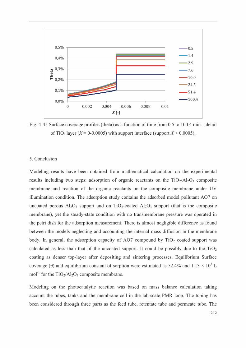
212
Fig. 4-45 Surface coverage profiles (theta) as a function of time from 0.5 to 100.4 min – detail
of TiO2 layer (X = 0-0.0005) with support interface (support X > 0.0005).
5. Conclusion
Modeling results have been obtained from mathematical calculation on the experimental
results including two steps: adsorption of organic reactants on the TiO2/Al2O3 composite
membrane and reaction of the organic reactants on the composite membrane under UV
illumination condition. The adsorption study contains the adsorbed model pollutant AO7 on
uncoated porous Al2O3 support and on TiO2-coated Al2O3 support (that is the composite
membrane), yet the steady-state condition with no transmembrane pressure was operated in
the petri dish for the adsorption measurement. There is almost negligible difference as found
between the models neglecting and accounting the internal mass diffusion in the membrane
body. In general, the adsorption capacity of AO7 compound by TiO2 coated support was
calculated as less than that of the uncoated support. It could be possibly due to the TiO2
coating as denser top-layer after depositing and sintering processes. Equilibrium Surface
coverage (θ) and equilibrium constant of sorption were estimated as 52.4% and 1.13 × 10⁴ L
mol-1 for the TiO2/Al2O3 composite membrane.
Modeling on the photocatalytic reaction was based on mass balance calculation taking
account the tubes, tanks and the membrane cell in the lab-scale PMR loop. The tubing has
been considered through three parts as the feed tube, retentate tube and permeate tube. The
0,0%
0,1%
0,2%
0,3%
0,4%
0,5%
0 0,002 0,004 0,006 0,008 0,01
Th
eta
X (-)
0.5
1.4
2.9
7.6
10.0
24.5
51.4
100.4

213
tanks have been studied with mass balance in the feed tank and permeate tank. And the
photocatalytic membrane cell was divided into retentate compartment, permeate compartment
and the membrane body to analyze the mass balance of the organic pollutant AO7. By
summarizing all the calculation, the modelled value was found in good agreement with
experimental data for optimized M100 membrane having decomposition rate constant kdec=
2.36 × 10⁻⁴ mol g-1 min-1 for AO7 aqueous compound. According to the AO7 concentration
profile, the changes of concentration inside the porous support, where the adsorption reaction
only is taken into account, is negligible. With decreasing concentration in the feed tank the
concentration gradient in TiO2 layer was reduced; as a result lower rate of adsorption and
decomposition of AO7 was oberved.

214

215
General conclusion and perspectives
The thesis is devoted to integrate TiO2 photocatalysis process with membrane separation
process aimed for degrading tedious organic pollution in water treatment technology. The
work has been carried out first by design of TiO2-based composite membrane, synthesis and
optimization of anatase TiO2 thin films, characterization of their main physico-chemical
properties and investigation of the functional performance of TiO2-coated membranes.
Plasma-enhanced chemical vapor deposition (PECVD) is a one-step method applied in the
thesis to deposit amorphous TiO2 thin film on different types of substrate at low temperature
in comparison to CVD method. PECVD operating conditions in particular as substrate
temperature (Ts), partial pressure of bring gas argon and precursor TTIP (PAr+TTIP), plasma
distance (dp) and RF power intensity (Wreal) have been studied with their influence on
deposition rate, Ti-O composite and thickness uniformity. Concerning a homogenous
deposited thickness and a reasonable surface energy in plasma/reaction process Ts = 150 °C
was decided based on the study of PECVD Ts from 50 – 250 °C. Moreover, PAr+TTIP = 0.225
mbar (0.155, 0.185 and 0.225 mbar studied) and dp = 3.0 cm (2.0, 2.5 and 3.0 cm studied)
were determined regarding to the richest Ti-O abundance and the smoothest thickness of the
thin film. More amounts of precursor vapor and longer times for diffusion in the gas phase
explain that the higher PAr+TTIP and longer dp could work as the optimal conditions. Since
Wreal = 65 W led to deposit with cracking surface due to stronger ion bombardment, Wreal = 50
W was maintained in the optimal PECVD protocol.
Afterward, post-annealing as-deposit at 300 °C for minimal staying time 4.5 h or at 400 °C
(no staying time needed) was proven being able to form crystalline anatase phase in
as-deposit thin film on silicon substrate according to XRD analysis. Pure anatase phase was
developed and maintained (no rutile or brookite phase was formed) by annealing the
supported TiO2 thin film from 300 to 700 °C. Crystallization annealing duration at 300 °C
could be shortened from 4.5 h for TiO2 on non-seeded silicon (made at Ts = 150 °C) to 1.5 h
for TiO2 on anatase-seeded silicon (obtained from sol dip-coating).
Chemistry of the amorphous and anatase TiO2 thin films (deposited on silicon) has been
interpreted from EDX and FTIR spectra. Chemical elements consisting of Ti, O, C, Si and Al
were detected in the as-deposit film. Existence of C and Al could be originated from residues
from the precursor (metal-organic compound TTIP) and alumina foil (protection wrap on the

216
bottom electrode) during plasma/reaction process. Signal of element Si is due to penetration
of incident X-ray through the thin film to silicon substrate as in EDX measurement. A
shoulder absorbance peak at wavenumber 700 cm-1 due to vibration of Ti-O was observed in
FTIR spectra of both amorphous and anatase films. Another sharp absorbance peak at
wavenumber 450 cm-1 was found characteristic for the obtained anatase film.
Physico-chemical properties of the optimal TiO2 thin film including crystalline structure,
microstructure, density, porosity, band gap, and surface hydrophilicity have been
characterized. It is found that the film has columnar alike microstructure in SEM scanning.
Mean thickness of the optimal film was known to be 1.3 μm (± 7% in full-scale surface area
12.6 cm2) with SEM cross-section analysis. Apparent density of the synthesized anatase layer
was found as 2.52 g cm-3 by modeling XRR curve and accordingly the porosity (i.e. void
volume percentage) was calculated as 33 % with knowing the density of dense anatase 3.87 g
cm-3. The cut-off absorbance by anatase thin film (supported on quartz) was found at 365 nm.
Therefore, band gap energy (Eg, 1.3 μm thick layer) was obtained as 3.30 eV by applying
Tauc plot on the UV/Vis absorbance spectrum, whereas Eg (180 nm thick layer) was known
as 3.15 eV by regressing Cauchy law on EP measurement from 1.25 – 3.50 eV. Crystal faces
of anatase phase (101), (004) and (200) at 2θ = 25.4°, 37.9° and 48.1° aspect were found in
the XRD pattern of anatase film. Complementary Raman scattering signal at 150 cm-1
characteristic for anatase materials was also observed on the obtained anatase thin film. Water
contact angle on anatase surface was reduced from 29° in darkness to 10° with 20-min UV
irradiation, which verified photo-induced hydrophilicity property.
Functional performance of the silicon-supported anatase thin film as photocatalyst was
examined with patented Pilkington assessment by self-removing stearic acid adhered on TiO2
surface in air under UV irradiation (35 W m-2, λ = 355 nm). At 50-min UV illumination
photodegraded rate of stearic acid (RST) on anatase-coated silicon reached 90% and after 80
min UV stearic acid was completely removed. No significant degradation was observed on
the uncoated substrate after 100 min of UV irradiation. The result is compared to a study of
photocatalytic characterization titania layers prepared at high temperature by conventional
CVD, in which UV device of intensity 32 W m-2 was used. For such dense layers (with stearic
acid only adsorbed at the external surface), a degradation rate of 90% was observed after a
time of UV irradiation ranging from 4 to 28 min relevant to deposition conditions [202]. In
another paper from our group dedicated to mesostructured anatase layers prepared by sol-gel

217
route and exhibiting a very high photocatalytic activity [119], the same degradation rate
requires an irradiation time of 10 s but with a 11 times larger irradiation power (380 W m-2).
Further on, anatase-coated porous alumina ceramics (i.e. the fabricated TiO2 composite
membrane) were tested in “static” condition under the effect of diffusion of the organic solute
in water. Membranes M100 (TiO2-layer thickness ≈ 1.3 μm) and M800 (TiO2-skin thickness ≤
0.5 μm) were made of PECVD anatase films on macroporous supports with deposition
durations equal to 20 min and 7 min respectively. Photodegrading efficiency of methylene
blue (MB) in water by periodically illuminated membranes M100 and M800 (UV source of
intensity 50 W m-2, λ = 355nm) was determined as dMB, the quantity of destroyed MB per unit
membrane surface area and per unit time. The value of dMB was obtained by calculating the
difference of diffused MB through the membrane either with or without UV irradiation. It has
been found that dMB equal to 2×10⁻⁸ mol m-2 s-1 for M100 and 1×10⁻⁸ mol m-2 s-1 for M800.
These results are in the same order of magnitude as those previously measured for titania
membranes prepared by sol-gel route in our group [14] or for Ag-titania-polymer composite
membranes in a very recent paper [203].
To follow up, the membranes were then tested in “dynamic” condition in the pressure-driven
membrane process in constructed pilot-scale unit. Water permeability through membranes
was first measured as 1800 L m-2 h-1 bar-1 and 8280 L m-2 h-1 bar-1 for M100 and M800 using
the reactor configuration of TiO2 surface in contact with permeate solution. With continuous
UV illumination (50 W m-2, λ = 355nm), membrane M100 performed about 5 times higher
photocatalytic efficiency (about 50% degraded MB from initial c0 = 3.2 × 10⁻⁷ mol L-1) than
that of M800 (about 10% degraded MB from initial c0 = 1.25 × 10⁻⁷ mol L-1) due to a slower
water permeability (at transmembrane pressure ΔP = 0.25 bar) and larger capacity dMB of
membrane M100. The experimental degradation rates are in very good accordance with
expected values (theoretically obtained from dMB), which proves the absence of defects on
membranes and pilot-scale unit. The reproducible performance was maintained on duplicate
membranes of each coating format of M100 and M800.
In parallel, influences of UV sources (power intensity and emission wavelength) and dynamic
membrane process (transmembrane pressure and circulation speed) on photodegradation rate
of acid orange 7 (AO7) and phenol were studied in lab-scale unit with the photocatalytic layer
in contact with the feed solution contained in the circulation loop of the photocatalytic

218
membrane reactor. With 4 W-powered UV irradiation for 2 h, destroyed AO7 per unit
membrane surface area was found 2.5 × 10⁻⁵ mol m-2 at emission wavelength λ = 365 nm and
2.0 × 10⁻⁵ mol m-2 at alternative λ = 254 nm. With 500 W-powered UV irradiation (UVA
emission from 360 nm) for 2 h, destroyed AO7 was found 3.5 × 10⁻⁴ mol m-2 by the same
membrane that is 10 times higher than that of using the low-intensity lamp. Self-photolysis
effect (uncoated ceramic support alone considered as non-photoactive) was found 2.8 × 10⁻⁶
mol m-2 (as 11% contribution to photodegradation) and 9.0 × 10⁻⁵ mol m-2 (as 26%
contribution to photodegradation) under 4 W and 500 W UV irradiation, respectively. Process
modeling (adsorption and photocatalysis reaction) was finally carried out from these available
experimental outputs.
Taking benefit of the quantification of the photocatalytic performance of the prepared
membranes with simplified membrane devices and with model organic molecule and of the
modeling results, the next stage should be to evaluate the membrane applicability considering
real urban or industrial waters and to scale-up of possible purification units.
In term of material engineering perspectives for the future research could be interested in
depositing TiO2 thin film with nitrogen dopant using additional N2 or NH3 in the PECVD
reactor. The band gap energy (Eg) of N-doped TiO2 can be narrowed since the non-metal
atoms (N in this case) as electron acceptors reduce the minimal energy levels in the
conduction band. Consequently, absorbance shift to the visible band can lead to solar
harvesting in photocatalytic water treatment technology.
Another possible valuation field for the developed PECVD-deposited TiO2 thin films could
be their integration in multilayer systems enabling water splitting and selective hydrogen
extraction.

219
Appendices
Appendix 1. Annual publications on TiO2 photocatalysis with (a) scientific papers and (b)
patens in water purification (∆!), air purification (u) and self-cleaning (¢). [40]

220
Appendix 2 Publications relevant to photocatalytic membrane and wastewater treatment from
January 2000 to September 2014 (an online survey based on “web of science”).
2000
2001
2002
2003
2004
2005
2006
2007
2008
2009
2010
2011
2012
2013
2014
0 30 60 90 120 150 180
Number of publications
Year
Topic on ''photocatalytic membrane''
2000
2001
2002
2003
2004
2005
2006
2007
2008
2009
2010
2011
2012
2013
2014
0 5 10 15 20 25
Number of publications
Year
Topic on ''photocatalytic membrane''
& ''wastewater treatment''
221
References
1. Tchobanoglous, G., Burton, L.F. and Stensel, H.D., Wastewater Engineering: Treatment
and Reuse 2002: Metcalf & Eddy.
2. Glaze, W., Kang, J.W. and Chapin, H.D., The Chemistry of Water Treatment Processes
Involving Ozone, Hydrogen Peroxide and Ultraviolet Radiation. J. Int. Ozone Assoc., 1987.
9(4): p. 335-352.
3. Koppenol, W.H.a.L., F.J., The oxidizing nature of the hydroxyl radical. A comparison with
the ferryl ion (FeO2+). J. Phys. Chem., 1984. 88(1): p. 99-101.
4. Fujishima, A.a.H., K., Electrochemical photolysis of water at a semiconductor electrode.
Nature, 1972. 238: p. 37-38.
5. Al-Ekabi, H.a.S., N., Kinetic studies in heterogeneous photocatalysis. 1. Photocatalytic
degradation of chlorinated phenols in aerated aqueous solutions onver TiO2 supported on
a galss matrix. J. Phys. Chem., 1988. 92(20): p. 5726-5731.
6. Grabowska, E., Reszczynska, J. and Zaleska, A., Mechanism of phenol photodegradation in
the presence of pure and modified-TiO2: A review. Water Res., 2012. 46(17): p. 5453-71.
7. Mozia, S., Toyoda, M., Inagaki, M., Tryba, B. and Morawski, A.W., Application of
carbon-coated TiO2 for decomposition of methylene blue in a photocatalytic membrane
reactor. J. Hazard. Mater., 2007. 140(1-2): p. 369-75.
8. Hájková, P., Špatenka, P., Krumeich, J., Exnar, P., Kolouch, A., Matoušek, J. and Kočí, P., Antibacterial effect of silver modified TiO2/PECVD films. Europ. Phys. J. D, 2009. 54(2): p.
189-193.
9. Nakano, R., Ishiguro, H., Yao, Y., Kajioka, J., Fujishima, A., Sunada, K., Minoshima, M.,
Hashimoto, K. and Kubota, Y., Photocatalytic inactivation of influenza virus by titanium
dioxide thin film. Photochem. Photobio. Sci., 2012. 11(8): p. 1293-1298.
10. Nakata, K.a.F., A., TiO2 photocatalysis: Design and applications. J. Photochem. and
Photobio. C: Photochem. Rev., 2012. 13(3): p. 169-189.
11. Ollis, D.F., Integrating photocatalysis and membrane technologies for water treatment: A
review. Ann. N. Y. Acad. Sci., 2003. 984: p. 65-83.
12. Mozia, S., Photocatalytic membrane reactors (PMRs) in water and wastewater treatment.
A review. Sep. Purif. Tech., 2010. 73(2): p. 71-91.
13. Athanasekou, C.P., Romanos, G.E., Katsaros, F.K., Kordatos, K., Likodimos, V. and Falaras,
P., Very efficient composite titania membranes in hybrid ultrafiltration/photocatalysis
water treatment processes. J. Membr. Sci., 2012. 392-393: p. 192-203.
14. Djafer, L., Ayral, A. and Ouagued, A., Robust synthesis and performance of a titania-based
ultrafiltration membrane with photocatalytic properties. Sep.Purif.Tech., 2010. 75(2): p.
198-203.
15. You, S.J., Semblante, U.S., Luc, S.C., Damodara, A.R. and Wei, T.C., Evaluation of the
antifouling and photocatalytic properties of poly(vinylidene fluoride) plasma-grafted
poly(acrylic acid) membrane with self-assembled TiO2. J. Hazard. Mater., 2012. 237-238:
p. 10-19.
16. Hu, A., Zhang, X., Oakes, D. K., Peng, P., Zhou, N. and Servos, R.M., Hydrothermal growth of
free standing TiO2 nanowire membranes for photocatalytic degradation of
pharmaceuticals. J. Hazard. Mater., 2011. 189(1-2): p. 278-285.
17. Zeng, Y., Cheng, G., Wen, M. and Wu, W., Effect of external bias voltage and coating
thickness on the photocatalytic activity of thermal sprayed TiO2 coating. Prog. Org. Coat.,
2007. 61(2-4): p. 321-325.
18. Choi, H., Stathatos, E. and Dionysiou, D.D., Sol–gel preparation of mesoporous
photocatalytic TiO2 films and TiO2/Al2O3 composite membranes for environmental
applications. Appl. Cat. B: Envir., 2006. 63(1-2): p. 60-67.

222
19. Vijayalakshmy, S.a.S., B., Enhanced performance of dye-sensitized solar cells with TiO2
blocking layers and Pt counter electrodes prepared by physical vapor deposition (PVD).
Electrochim. Acta., 2014. 116(0): p. 334-342.
20. Ragazzon, D., Farstad, M. H., Schaefer, A., Walle, L. E., Uvdal, P., Borg, A. and Sandell, A.,
Growth of TiO2(B)(001) on Au(111) by chemical vapor deposition. Surf. Sci., 2015. 633: p.
102-108.
21. Kulisch, W., Remote plasma-enhanced chemical vapour depoisiton with metal organic
source gases: principles and applications. Surf. Coat. Tech., 1993. 59: p. 193-201.
22. Stroyuk, L.A., Kryukov, I.A., Kuchimii, Y.S. and Pokhodenko, D.V., Quantum effects in
semiconductor photocatalysis. Theor. Exp. Chem., 2005. 41(4): p. 207-228.
23. Agrios, G.A.a.P., P., Recombination rate of photogenerated charges versus surface area:
Opposing effects of TiO2 sintering temperature on photocatalytic removal of phenol,
anisole, and pyridine in water. J. Photochem. Photobio. A: Chem., 2006. 180(1–2): p.
130-135.
24. Chen, D., Li, F and Ray, K.A., Effect of mass transfer and catalyst layer thickness on
photocatlaytic reaction. AIChE J., 2000. 46(5): p. 1034-1045.
25. Huang, S.S.a.C., J.S., Comparison of the characteristics of TiO2 films prepared by
low-pressure and plasma-enhanced chemical vapor deposition. J. Mater. Sci.: Mater. Elec.,
2002. 13(2): p. 77-81.
26. Wu, C.Y., Chiang, B. S., Chang, S. and Liu, D. S., Determination of photocatalytic activity in
amorphous and crystalline titanium oxide films prepared using plasma-enhanced chemical
vapor deposition. Applied Surface Science, 2011. 257(6): p. 1893-1897.
27. Srivatsa, K.M.K., Bera, M. and Basu, A., Preparation of large surface area rutile titania
crystals at room temperature by PECVD with applied d.c. bias. Mater. Lett., 2008. 62(20):
p. 3527-3529.
28. Li, D., Carette, M., Granier, A., Landesman, J.P. and Goullet, A., In situ spectroscopic
ellipsometry study of TiO2 films deposited by plasma enhanced chemical vapour deposition.
Applied Surface Science, 2013. 283: p. 234-239.
29. Lacoste, A., PBII processing of dielectric layers: physical aspects limitations and
experimental results. Surf. Coat. Tech., 2001. 135(2-3): p. 268-273.
30. Lacoste, A.a.P., J., Processing considerations with plasma-based ion implantation of
polymers: Theoretical aspects, limitations, and experimental results. Nuc. Instr. Meth. Phys.
Res. Sec. B: Beam Inter. Mater. Atom., 2003. 208: p. 260-266.
31. Zhou, M., Roualdès, S., Zhao, J., Autès,V. and Ayral, A., Nanocrystalline TiO2 thin film
prepared by low-temperature plasma-enhanced chemical vapor deposition (PECVD) for
photocatalytic applications. Thin Solid Filmes, 2015. accepted.
32. P/N junctions and band gaps. 2011; http://solarcellcentral.com/junction_page.html
Copyright © 2011 Four Peaks Technologies].
33. Linsebigler, A.L., Lu, G.Q. and Yates, J.T., Photocatalysis on TiO2 surfaces: Principles
mechanisms and selected results. Chemi. Rev., 1995. 95(3): p. 735-758.
34. Murphy, A., Band-gap determination from diffuse reflectance measurements of
semiconductor films, and application to photoelectrochemical water-splitting. Solar
Energy Materials and Solar Cells, 2007. 91(14): p. 1326-1337.
35. Fox, A.M.a.D., T.M., Heterogeneous photocatalysis Chem. Rev., 1993. 93(1): p. 341-357.
36. Zhang, J., Zhou, P., Liu, J. and Yu, J., New understanding of the difference of photocatalytic
activity among anatase, rutile and brookite TiO2. Phys. Chem. Chem. Phys., 2014. 16(38):
p. 20382-6.
37. Direct and indirect band gap semiconductors. 2015;
http://www.doitpoms.ac.uk/tlplib/semiconductors/direct.php Copyright © 2004-2015
University of Cambridge].
38. Fujishima, A., Zhang, X. and Tryk, D.A., TiO2 photocatalysis and related surface
phenomena. Surf. Sci. Rep., 2008. 63(12): p. 515-582.

223
39. Schneider, J., Matsuoka, M., Takeuchi, M., Zhang, J., Horiuchi, Y., Anpo, M. and Bahnemann,
W.D., Understanding TiO2 photocatalysis: mechanisms and materials. Chem. Rev., 2014.
114(19): p. 9919-86.
40. Ochiai, T. and A. Fujishima, Photoelectrochemical properties of TiO2 photocatalyst and its
applications for environmental purification. J. Photochem. and Photobio. C: Photochem.
Rev., 2012. 13(4): p. 247-262.
41. Peiró, M.A., Colombo, C., Doyle, G., Nelson, J., Mills, A. and Durrant, R.G., Photochemical
reduction of oxygen adsorbed to nanocrystalline TiO2 films: A transient absorption and
oxygen scavenging study of pifferent TiO2 preparations. J. Phys. Chem., 2006. 110: p.
23255–23263.
42. Tamaki, Y., Furube, A., Murai, M., Hara, K., Katoh, R. and Tachiya, M., Dynamics of efficient
electron–hole separation in TiO2 nanoparticles revealed by femtosecond transient
absorption spectroscopy under the weak-excitation condition. Phys. Chem. Chem. Phys. ,
2007. 9: p. 1453-1460.
43. Yamakata, A., Ishibashi, T. and Onishi, H., Water-and oxygen-induced decay kinetics of
photogenerated electrons in TiO2 and Pt/TiO2: A time-resolved infrared absorption study.
J. Phys. Chem. B 105 (2001) 2001. 105(30): p. 7258-7262.
44. Yoshihara, T., Katoh, R. , Furube, A., Tamaki, Y., Murai, M., Hara, K., Murata, S., Arakawa,
H. and Tachiya, M. , Identification of reactive species in photoexcited nanocrystalline TiO2
films by wide-wavelength-range (400−2500 nm) transient absorption spectroscopy. J. Phys.
Chem. B, 2004. 108(12): p. 3817-3823.
45. Colombo, D.P., Jr., and Bowman M.B., Does interfacial charge transfer compete with charge
carrier recombination? A femtosecond diffuse reflectance onvestigation of TiO2
manoparticles. J. Phys. Chem., 1996. 100(47): p. 18445–18449.
46. Tamaki, Y., Furube, A. , Murai, M., Hara, K., Katoh, R. and Tachiya, M. , Direct observation
of reactive trapped holes in TiO2 undergoing photocatalytic pxidation of adsorbed
Alcohols: Evaluation of the reaction rates and yields. J. Am. Chem. Soc., 2006. 128: p.
416-417.
47. Hurum, D.C., Agrios, A.G., Gray, K.A., Rajh, T. and Thurnauer, M.C. , Explaining the
enhanced photocatalytic activity of Degussa P25 mixed-phase TiO2 using EPR. J. Phys.
Chem. B, 2003. 107: p. 4545-4549.
48. Micic, O., Zhang, Y., Cromack, K.R., Trifunac, A. and Thurnauer, M. , Photoinduced hole
transfer from titanium dioxide to methanol molecules in aqueous solution studied by
electron paramagnetic resonance. J. Phys. Chem. , 1993. 97: p. 13284-13288.
49. Szczepankiewicz, S.H., Colussi, A.J. and Hoffmann, M.R. , Infrared spectra of photoinduced
species on hydroxylated titania surfaces. J. Phys. Chem. B, 2000. 104: p. 9842-9850.
50. Valentin, D.C., Pacchioni, G. and Selloni, A. , Electronic structure of defect states in
hydroxylated and reduced rutile TiO2(110) surfaces. Phys. Rev. Lett., 2006. 97: p.
166803-166804.
51. Henderson, A.M., A surface science perspective on View the MathML source photocatalysis.
Surf. Sci. Rep., 2011. 66(6-7): p. 185-297.
52. Hoffmann, M.R., Martin, S.T., Choi, W. and Bahnemann, D.W., Environmental
applications of semiconductor photocatalysis. Chem. Rev. , 1995. 95(1): p. 69-96.
53. Salvador, P.a.G., C., The nature of surface states involved in the photo- and
electroluminescence spectra of n-titanium dioxide electrodes. J. Phys. Chem. , 1984.
88(16): p. 3696-3698.
54. Nakamura, R., Ohashi, N., Imanishi, A., Osawa, T., Matsumoto, Y., Koinuma, H. and Nakato,
Y., Crystal-face dependences of surface band edges and hole reactivity, revealed by
preparation of essentially atomically smooth and stable (110) and (100) n-TiO2 (rutile)
surfaces. J. Phys. Chem. B, 2005. 109: p. 1648-1651.
55. Murakami, Y.M.K., E., Nosaka, A.Y. and Nosaka, Y., Direct detection of OH radicals diffused
to the gas phase from the UV-irradiated photocatalytic TiO2 surfaces by means of

224
laser-induced fluorescence spectroscopy. J. Phys. Chem. B, 2006. 110(34): p.
16808-16811.
56. Zhang, J. and Y. Nosaka, Mechanism of the OH radical generation in photocatalysis with
TiO2 of different crystalline types. J. Phys. Chem. C., 2014. 118(20): p. 10824-10832.
57. Draper, R.B.a.F., M.A. , Titanium dioxide photosensitized reactions studied by diffuse
reflectance flash photolysis in aqueous suspensions of TiO2 powder. Langmuir, 1990. 6(8):
p. 1396-1402.
58. Tachikawa, T., Tojo, S. Fujitsuka, M. and Majima, T., Photocatalytic one-electron oxidation
of biphenyl derivatives strongly coupled with the TiO2 surface. Langmuir, 2004. 20(7): p.
2753-2759.
59. Nosaka, Y., Komori, S., Yawata, K., Hirakawa, T. and Nosaka, A.Y., Photocatalytic ˙OH
radical formation in TiO2 aqueous suspension studied by several detection methods. Phys.
Chem. Chem. Phys. , 2003. 5: p. 4731-4735.
60. Hwang, S.J., Petucci, C. and Raftery, D., In situ solid-state NMR studies of trichloroethylene
photocatalysis: Formation and characterization of surface-bound Intermediates. J. Am.
Chem. Soc., 1998. 120(18): p. 4388-4397.
61. Nosaka, Y., Daimon, T., Nosaka, A.Y. and Murakami, Y., Singlet oxygen formation in
photocatalytic TiO2 aqueous suspension. Phys. Chem. Chem. Phys., 2004. 6: p. 2917-2918.
62. Chen, C.C., Lu, C.S., Chung, Y.C. and Jan, J.L., UV light induced photodegradation of
malachite green on TiO2 nanoparticles. J. Hazard. Mater., 2007. 141: p. 520-528.
63. Bhatkhnade, D.S., Kamble, S.P., Sawant, S.B., and Pangarkar, V.G., Photocatalytic and
photochemical degradation of nitrobenzene using artificial ultraviolet light. Chem. Eng. J.,
2004. 102: p. 283-290.
64. Chong, M.N., Lei, S., Jin, B., Saint, C. and Chow, C.W.K., Optimizaion of an annular
photoreactor process for degradation of Congo red using a newly synthesized titania
impregnated kaolinite nano-photocatalyst. Sep. Purif. Tech., 2009. 67: p. 355-363.
65. Gaya, U.I. and A.H. Abdullah, Heterogeneous photocatalytic degradation of organic
contaminants over titanium dioxide: a review of fundamentals, progress and problems. J.
Photochm. Photobiol. C: photochem. Rev., 2008. 9: p. 1-12.
66. Renz, C., Lichtreaktionen der oxyde des titans, cers und der erdsäuren. Helv. Chim. Acta.,
1921. 4: p. 961-968.
67. Goodeve, C.F.a.K., J.A., Photosensitisation by titanium dioxide. Trans. Faraday Soc., 1938.
34(1): p. 570-579.
68. Goodeve, C.F.a.K., J.A., The mechanism of photosensitisation by solids. Tran. Faraday Soc.,
1938. 34: p. 902-908.
69. Markham, M.C. and K.J. Laidler, A kinetic study of photo-oxidations on the surface of zinc
oxide in aqueous suspensions. J. Phys. Chem., 1953. 57: p. 363-369.
70. Stephens, R.E., Ke, B. and Trivich D. , The efficiencies of some solids as catalysts for the
photosynthesis of hydrogen peroxide. J. Phys. Chem. , 1955. 59: p. 966-969.
71. Kennedy, R.D., Ritchie, M. and Mackenzie, J. , The photosorption of oxygen and nitric oxide
on titanium dioxide
. Trans. Faraday Soc., 1958. 54: p. 130-138.
72. Filimonov, N.V., Photocatalytic Oxidation of gaseous isopropanol on ZnO and TiO2 Doklady
Akademii Nauk SSSR, 1964. 154: p. 922-925.
73. Kato, S. and F. Mashio, TiO2 photocatalyzed oxidation of tetraline in liquid phase. J. Chem.
Soc. Japan., Indust. Chem. Sect. , 1964. 67: p. 1136-1140.
74. McLintock, S.I. and M. Ritchie, Reactions on titanium dioxide: Photo-adsorption and
oxidation of ethylene and propylene. Trans. Faraday Soc., 1965. 61: p. 1007-1016.
75. Frank, S.N.a.B., J.A., Heterogeneous photocatalytic oxidation of cyanide and sulfite in
aqueous solutions at semiconductor powders. J. Phys. Chem., 1977. 81: p. 1484–1488.

225
76. Frank, S.N. and A.J. Bard, Heterogeneous photocatalytic oxidation of cyanide ion in
aqueous solution at TiO2 powder. J. Am. Chem. Soc., 1977. 99: p. 303-304.
77. Noguchi, T., Fujishima, A., Sawunyama, P. and Hashimoto, K., Photocatalytic degradation
of gaseous formaldehyde using TiO2 film. Environ. Sci. Tech., 1998. 32(3831-3833).
78. Obuchi, E., Sakamoto, T., Nakano, K. and Shiraishi, F., Photocatalytic decomposition of
acetaldehyde over TiO2/SiO2 catalyst. Chem. Eng. Sci., 1999. 54: p. 1525-1530.
79. Alberici, M.R. and F.W. Jardim, Photocatalytic destruction of VOCs in the gas-phase using
titanium dioxide. Appl. Catal. B: Environ., 1997. 14: p. 55-68.
80. Ollis, D.F., Pelizzetti, E. and Serpone, N., , Photochemical conversion and storage of solar
energy. Environ. Sci. Tech., 1991. 25.
81. Fei, H., Leng, W., Li, X., Cheng, X., Xu, Y., Zhang, J. and Cao, C., Photocatalytic oxidation of
arsenite over TiO2: Is superoxide the main oxidant in normal air-saturated aqueous
solution? Environ. Sci. Technol., 2011. 45: p. 4352-4539.
82. Sunada, K., Watanabe, T. and Hashimoto, K, Studies on photokilling of bacteria on TiO2
thin film. J. Photochem. Photobio. A: Chem., 2003. 156: p. 227-233.
83. Sclafani, A. and J.M. Herrmann, Comparison of the photoelectronic and photocatalytic
activities of various anatase and rutile forms of titania in pure liquid organic phases and in
aqueous solutions. J. Phys. Chem., 1996. 100(32): p. 13655-13661.
84. Yang, D., Liu, H., Zheng, Z., Yuan, Y., Zhao, J., Waclawik, E.R., Ke, X. and H. and Zhu, An
efficient photocatalyst structure: TiO2(B) nanofibers with a shell of anatase nanocrystals. J.
Am. Chem. Soc., 2009. 131(49): p. 17885-17893.
85. Collins-Martinez, V., A.L. Ortiz, and A.A. Elguezabal, Influence of the anatase/rutile ratio
on the TiO2 photocatalytic activity for the photodegradation of light hydrocarbons.
International Journal of Chemical Reactor Engineering, 2007. 5.
86. Di Paola, A., Bellardita, M. and Palmisano, L., Brookite, the least known TiO2 photocatalyst.
Catalysts, 2013. 3(1): p. 36-73.
87. Srivatsa, K.M.K., Bera, M. and Basu, A., Pure brookite titania crystals with large surface
area deposited by plasma enhanced chemical vapour deposition technique. Thin Solid
Films, 2008. 516(21): p. 7443-7446.
88. Moellmann, J., Ehrlich, S., Tonner, R. and Grimme, S., A DFT-D study of structural and
energetic properties of TiO2 modifications. J. Phys.: Condens. Matter., 2012. 24(42).
89. Ishioka, K. and H. Petek, Raman generation of coherent phonons of anatase and rutile TiO2
photoexcited at fundamental absorption edges. Phys. Rev. B
, 2012. 86.
90. Alberti, A., Bongiorno, C. and Pellegrino, G., Anatase/rutile nucleation and growth on
(0002) and (11-20) oriented ZnO:Al/glass substrates at 150°C. Thin Solid Films, 2014.
555: p. 3-8.
91. Hengerer, R., Bolliger, B., Erbudak, M. and Grätzel, M., Structure and stability of the
anatase TiO2 (101) and (001) surfaces. Surf. Sci., 2000. 460: p. 162-169.
92. Burnside, D.S., Shklover, V., Barbe, C., Comte, P., Arendse, F., Brooks, K. and Grätzel, M.,
Self-organization of TiO2 nanoparticles in thin films. Chem. Mater., 1998. 10: p.
2419-2425.
93. Ruzycki, N., Herman, C.S., Boatner, A.L. and Diebold, U., Scanning tunneling microscopy
study of the anatase (100) surface. Surf. Sci., 2003. 529: p. L239-L244.
94. Shklover, V., Nazeeruddin, K.M., Zakeeruddin, M.S., Barbe, C., Kay, A., Haibach, T., Steurer,
W., Hermann, R., Nissen, U.H and Grätzel, M., Structure of nanocrystalline TiO2 powders
and precursor to their highly efficient photosensitizer. Chem. Mater. , 1997. 9(2): p.
430-439.
95. Pan, J., Liu, G., Lu, G.Q. and Cheng, H.M., On the true photoreactivity order of {001}, {010},
and {101} facets of anatase TiO2 crystals. Angew. Chem. Int. Ed., 2011. 50(9): p.
2133-2137.
226
96. Ramamoorthy, M., Vanderbilt, D. and King-Smith, D.R., First-principles calculations of the
energetics of stoichiometric TiO2 surfaces. Phys. Rev. B, 1994. 49.
97. Beltrán, A., Gracia, L. and Andrés, J., Density functional theory study of the brookite
surfaces and phase transitions between natural titania polymorphs. J. Phys. Chem. B, 2006.
110: p. 23417-23423.
98. López, R. and R. Gómez, Band-gap energy estimation from diffuse reflectance
measurements on sol–gel and commercial TiO2: A comparative study. J. Sol-Gel Sci. Tech.,
2011. 61(1): p. 1-7.
99. Valencia, S., Marin, M.J. and G. and Restrepo, Study of the bandgap of synthesized titanium
dioxide nanoparticules using the sol-gel method and a hydrothermal treatment. Open
Mater. Sci. J., 2010. 4: p. 9-14.
100. Kaur, K. and C.V. Singh, Amorphous TiO2 as a photocatalyst for hydrogen production: A
DFT study of structural and electronic properties. Energ. Proc., 2012. 29: p. 291-299.
101. Lee, Y.C., Chang, Y.S., Teoh, L.G., Huang, Y.L. and Shen, Y.C., The effects of the nanostructure
of mesoporous TiO2 on optical band gap energy. J. Sol-Gel Sci. Tech., 2010. 56(1): p. 33-38.
102. Tian, G.L., He, H. B. and Shao, J.D., Effet of microstructure of TiO2 thin films on optical band
gap energy. Chin. Phys. Lett, 2005. 22(7): p. 1787-1790.
103. Liu, G., Wang, L., Sun, C., Yan, X., Wang, X., Chen, Z., Smith, C.S., Cheng, H.M. and Lu, G.Q.,
Band-to-band visible-light photon excitation and photoactivity induced by homogeneous
nitrogen doping in layered titanates. Chem. Mater., 2009. 21(7): p. 1266-1274.
104. Romero-Gomez, P., Rico, V., Borras, A., Barranco, A. , Espinos, P.J., Cotrino, J. and
Gonzalez-Elipe, R.A., Chemical state of nitrogen and visible surface and schottky barrier
driven photoactivities of N-Doped TiO2 thin films. J. Phys. Chem. C 2009. 113(30): p.
13341–13351.
105. Wu, Y., Xing, M., Tian, B., Zhang, J. and Chen, F., Preparation of nitrogen and fluorine
co-doped mesoporous TiO2 microsphere and photodegradation of acid orange 7 under
visible light. Chem. Eng. J., 2010. 162(2): p. 710-717.
106. Maeda, M. and T. Watanabe, Visible light photocatalysis of nitrogen-doped titanium oxide
films prepared by plasma-enhanced chemical vapor deposition. J. Electrochem. Soc., 2006.
153(3): p. 186-189.
107. Zhang, L. and J.C. Yu, A sonochemical approach to hierarchical porous titania spheres with
enhanced photocatalytic activity. Chem. Comm., 2003(16): p. 2078.
108. Alem, A. and H. Sarpoolaky, The effect of silver doping on photocatalytic properties of
titania multilayer membranes. Solid State Sci., 2010. 12(8): p. 1469-1472.
109. Liu, R., Wang, P., Wang, X., Yu, H. and Yu, J., UV- and visible-light photocatalytic activity of
simultaneously deposited and doped Ag/Ag(I)-TiO2 photocatalyst. J. Phys. Chemi. C, 2012.
116(33): p. 17721-17728.
110. Benotti, M.J., Stanford, B.D., Wert, E.C. and Snyder, S.A., Evaluation of a photocatalytic
reactor membrane pilot system for the removal of pharmaceuticals and endocrine
disrupting compounds from water. Water Res., 2009. 43(6): p. 1513-1522.
111. Mozia, S., Tomaszewska, M. and Morawski, A.W., Photocatalytic membrane reactor (PMR)
coupling photocatalysis and membrane distillation—Effectiveness of removal of three azo
dyes from water. Cat. Today, 2007. 129(1-2): p. 3-8.
112. Sobczyński, A., Duczmal, Ł. and Zmudziński, W., Phenol destruction by photocatalysis on
TiO2: an attempt to solve the reaction mechanism. J. Molec. Cat. A: Chemi., 2004. 213(2):
p. 225-230.
113. Andreozzi, R., Caprio, V., nsola, A. and Marotta, R., Advanced oxidation processes (AOP) for
water purification and recovery. Cat. Today, 1999. 53: p. 51-59.
114. Moslehyani, A., Ismail, A. F., Othman, M.H.D. and Matsuura, T., Hydrocarbon degradation
and separation of bilge water via a novel TiO2-HNTs/PVDF-based photocatalytic
membrane reactor (PMR). RSC Adv., 2015. 5(19): p. 14147-14155.
227
115. Ayllon, J.A., Figueras, A., Garelik, S., Spirkova, L., Durand, J. and Cot, L., Preparation of TiO2
powder using titanium tetraisopropoxide decomposition in a plasma enhanced chemical
vapor deposition (PECVD) reactor. J. Mater. Sci. Lett., 1999. 18: p. 1319-1321.
116. Kment, Š., Gregora, I.. Kmentová, H., Novotná, P., Hubička, Z., Krýsa, J., Sajdl, P., Dejneka, A., Brunclíková, M., Jastrabík, L. and Hrabovský, M., Raman spectroscopy of dip-coated and
spin-coated sol–gel TiO2 thin films on different types of glass substrate. Journal of Sol-Gel
Science and Technology, 2012. 63(3): p. 294-306.
117. Krýsa, J., Baudys, M., Zlámal, M., Krýsová, H., Morozová, M. and Klusoň, P., Photocatalytic
and photoelectrochemical properties of sol–gel TiO2 films of controlled thickness and
porosity. Cat. Today, 2014. 230: p. 2-7.
118. Molinari, R., Pirillo, F., Loddo, V. and Palmisano, L., Heterogeneous photocatalytic
degradation of pharmaceuticals in water by using polycrystalline TiO2 and a nanofiltration
membrane reactor. Cat. Today, 2006. 118(1-2): p. 205-213.
119. Bosc, F., Ayral, A., Albouy, P. A. and Guizard, C., A simple route for low-temperature
synthesis of mesoporous and nanocrystalline anatase thin films. Chem. Mater., 2003.
15(12): p. 2463-2468.
120. Ayral, A., Guizard, L. and Cot, L., Synthesis and application of hybrid organic-inorganic
colloidal gels. J. Mater. Sci. Lett., 1994. 13: p. 1538-1539.
121. Shon, K.H., Phuntsho, S. and Vigneswaran, S., Effect of photocatalysis on the membrane
hybrid system for wastewater treatment. Desalination, 2008. 225(1-3): p. 235-248.
122. Chu, S., Luo, L., Yang, J., Kong, F., Luo, S., Wang, Y. and Zou, Z., Low-temperature synthesis
of mesoporous TiO2 photocatalyst with self-cleaning strategy to remove organic templates.
Appl. Surf. Sci., 2012. 258(24): p. 9664-9667.
123. Bosc, F., Ayral, A. and Guizard, C., Mesoporous anatase coatings for coupling membrane
separation and photocatalyzed reactions. J. Membr. Sci., 2005. 265(1-2): p. 13-19.
124. Bosc, F., Lacroix-Desmazes, P. and Ayral, A., TiO2 anatase-based membranes with
hierarchical porosity and photocatalytic properties. J. Colloid. Interface. Sci., 2006. 304(2):
p. 545-548.
125. Kim, G.M., Lee, S.M., Michler, G.H., Roggendorf, H., Gosele, U. and Knez, M., Nanostructured
pure anatase titania tubes replicated from electrospun polymer fiber templates by atomic
layer deposition. Chem. Mater., 2008. 20(9): p. 3085-3091.
126. Leong, S., Razmjou, A., Wang, K., Hapgood, K., Zhang, X. and Wang, H., TiO2 based
photocatalytic membranes: A review. J. Membr. Sci., 2014. 472: p. 167-184.
127. Zhang, X., Wang, D.K. and J.C. and Diniz da Costa, Recent progresses on fabrication of
photocatalytic membranes for water treatment. Cat. Today, 2014. 230: p. 47-54.
128. Pelaez, M., Nolan, T.N., Pillai, C.S., Seery, K.M., Falaras, P., Kontos, G.A., Dunlop, S.M.P.,
Hamilton, Jeremy, J.W., Byrne, J. A., O'Shea, K., Entezari, H.M. and Dionysiou, D.D., A
review on the visible light active titanium dioxide photocatalysts for environmental
applications. Appl. Cat. B: Environ., 2012. 125: p. 331-349.
129. Zhang, X., Zhang, T., Ng, J., and Sun, D.D., High-performance multifunctional TiO2 nanowire
ultrafiltration membrane with a hierarchical layer structure for water treatment. Adv.
Funct. Mater., 2009. 19: p. 3731–3736.
130. Zhang, X., Du, A.J., Lee, P., Sun, D.D. and Leckie, O.J., TiO2 nanowire membrane for
concurrent filtration and photocatalytic oxidation of humic acid in water. J. Membr. Sci.,
2008. 313: p. 44-51.
131. Albu, P.S., Ghicov, A., Macak, M.J., Hahn, R. and Schmuki, P., Self-organized, free-standing
TiO2 nanotube membrane for flow-through photocatalytic applications. Nano Lett. , 2007.
7: p. 1286–1289.
132. Liao, J., Lin, S., Pan, N., Li, S., Cao, X. and Cao, Y., Fabrication and photocatalytic properties
offree-standingTiO2 nanotube membranes with through-hole morphology. Mater. Charact.,
2012. 66: p. 24-29.

228
133. Zhang, X., Du,J.A., Lee, P., Sun, D.D. and Leckie,O.J., Grafted multifunctional titanium
dioxide nanotube membrane: separation and photodegradation of aquatic pollutant. Appl.
Catal. B: Environ., 2008. 84: p. 262-267.
134. Zhang, X.W., D.K., Lopez, D.R.S and Costa, J.C.D.D, Chem. Eng. J. , 2013.
135. Liu, L., Liu, Z., Bai, H., Sun, D.D., Concurrent filtration and solar photocatalytic
disinfection/degradation using high-performance Ag/TiO2 nanofiber membrane. Water
Res., 2012. 46: p. 1101-1112.
136. Song, H., Shao, J., He,Y., Liu, B. and Zhong, X., Natural organic matter removal and flux
decline with PEG-TiO2-doped PVDF membranes by integration of ultrafiltration with
photocatalysis. J. Membr. Sci., 2012. 405-406: p. 48-56.
137. Rahimpour, A., Madaeni, S.S., Taheri, A.H. and Mansourpanah, Y., Coupling TiO2
nanoparticles with UV irradiation for modification of polyethersulfone ultrafiltration
membranes. J.Membr.Sci.313(2008). 2008. 313: p. 158-169.
138. Rahimpour, A., Jahanshahi, M., Rajaeian, B. and Rahimnejad, M., TiO2 entrapped
nano-composite PVDF/PES membranes: Preparation, characterization, antifouling and
antibacterial properties. Desalination, 2011. 278: p. 343-353.
139. Damodar, A.R., You, S.J. and Chou, H.H., Study the self cleaning, antibacterial and
photocatalytic properties of TiO2 entrapped PVDF membranes. J. Hazard. Mater., 2009.
172: p. 1321-1328.
140. Mansourpanah, Y., Madaeni, S.S., Rahimpour,A., Farhadian, F. and Taheri, A.H., Formation
of appropriate sites on nanofiltration membrane surface for binding TiO2 photo-catalyst:
performance,characterization and fouling-resistant capability. J. Membr. Sci. , 2009. 330:
p. 297-306.
141. Bredow, T. and K. Jug, SINDO1study of photocatalytic formation and reactions of OH
radicals at anatase particles. J. Phys. Chem., 1995. 99: p. 285-291.
142. Kim, S.H., Kwak, S.Y., Sohn,B.H. and Park, T.H., Design of TiO2 nanoparticle self-assembled
aromatic polyamide thin-film-composite (TFC) membrane as an approach to solve
biofouling problem. J. Membr. Sci., 2003. 211: p. 157-165.
143. Zhang, H., Quan, X., Chen, S. and Zhao, H., Fabrication and characterization of
silica/titania nanotubes composite membrane with photocatalytic capability. Environ. Sci.
Tech., 2006. 40: p. 6104-6109.
144. Ma, N., Zhang, Y., Quan, X., Fan, X. and Zhao, H., Performing a microfiltration integrated
with photocatalysis using an Ag-TiO2/HAP/Al2O3 composite membrane for water
treatment: Evaluating effectiveness for humic acid removal and anti-fouling properties.
Water Res. , 2010. 44: p. 6104-6114.
145. Ke, X., Ribbens, S., Fan, Y., Liu, H., Cool, P., Yang D. and H. Zhu, H., Integrating efficient
filtration and visible-light photocatalysis by loading Ag-doped zeolite Y particles on
filtration membrane of alumina nanofibers. J. Membr. Sci. , 2011. 375: p. 69-74.
146. Romanos, E.G., Athanasekou, P.C., Katsaros, K.F., Kanellopoulos, K.N., Diony-siou, D.D.,
Likodimos, V. and Falaras, P., Double-side active TiO2-modified nanofiltration membranes
in continuous flow photocatalytic reactors for effective water purification. J. Hazard. Mater.
, 2012. 211-212: p. 304–316.
147. Lin, Y.F., Tung, K.L., Tzeng, Y.S., Chen, J.H. and Chang, K.S., Rapid atmospheric plasma
spray coating preparation and photocatalytic activity of macroporous titania
nanocrystalline membranes. J. Membr. Sci., 2012. 389: p. 83-90.
148. Rowlette, C.P. and A.C. Wolden, Pulsed plasma-enhanced chemical vapor deposition of
Al2O3–TiO2 nanolaminates. Thin Solid Films, 2010. 518(12): p. 3337-3341.
149. Hong, H.J., Sarkar, K.S. and Lee, B.T., Formationof TiO2 nano fibers on a microchanneled
Al2O3–ZrO2/TiO2 porous composite membrane for photocatalytic filtration. J. Eur.
Ceram. Soc. , 2012. 32: p. 657-663.
229
150. Frach, P., et al., Pulse Magnetron Sputtering with high power density – an attempt at a
critical evaluation. IOP Conference Series: Materials Science and Engineering, 2012. 39:
p. 012007.
151. Horáková, M., et al., Sputter deposition of nanostructured TiO2 thin films. IEEE
Transactions on Plasma Science, 2014. 42(10): p. 2790-2791.
152. Moser, E.M., Chappuis, S. and Olleros, J., Production of photocatalytically active titania
layers: A comparison of plasma processes and coating properties. Surf. Coat.Tech., 2013.
227: p. 2-9.
153. Tavares, C.J., et al., PVD-Grown photocatalytic TiO2 thin films on PVDF substrates for
sensors and actuators applications. Thin Solid Films, 2008. 517(3): p. 1161-1166.
154. Zeman, P. and S. Takabayashi, Nano-scaled photocatalytic TiO2 thin films prepared by
magnetron sputtering. Thin Solid Films, 2003. 433(1-2): p. 57-62.
155. Horprathum, M., et al., Fabrication of nanostructure by physical vapor deposition with
glancing angle deposition technique and its applications. 2014: p. 7-11.
156. Heinrichs, J., Jarmar, T., Wiklund, U., and Engqvist, H., Physical vapour deposition and
bioactivity of crystalline titanium dioxide thin films. Trends Biomater. Artif. Organs, 2008.
22(2): p. 104-110.
157. Frach, P., et al., Deposition of photocatalytic TiO2 layers by pulse magnetron sputtering
and by plasma-activated evaporation. Vacuum, 2006. 80(7): p. 679-683.
158. Alvarez, R., Romero-Gomez, P., Gil-Rostra, J., Cotrino, J., Yubero, F., Gonzalez-Elipe, A.R.
and Palmero, A., Growth of SiO2 and TiO2 thin films deposited by reactive magnetron
sputtering and PECVD by the incorporation of non-directional deposition fluxes. Phys. Stat.
Solid (A), 2013. 210(4): p. 796-801.
159. Bhattacharyya, D., Sahoo, N.K., Thakur, S. AND Das, N.C. , Spectroscopic ellipsometry of
TiO2 layers prepared by ion-assisted electron-beam evaporation. Thin Solid Films, 2000.
360: p. 96-102.
160. Giolli, C., et al., Characterization of TiO2 coatings prepared by a modified electric
arc-physical vapour deposition system. Surface and Coatings Technology, 2007. 202(1): p.
13-22.
161. Rico, V., Romero, P., Hueso, L.J, Espinós, P.J. and González-Elipe, R.A., Wetting angles and
photocatalytic activities of illuminated TiO2 thin films. Cat. Today, 2009. 143(3-4): p.
347-354.
162. Bai, H., Liu, Z. and Sun, D.D., Hierarchically multifunctional TiO2 nano-thorn membrane for
water purification. Chem. Commun. , 2010. 46: p. 6542-6544.
163. Cao, X.P., Li, D., Jing, W.H., Xing, W.H. and Fan, Y.Q., Synthesis of visible-light responsive C, N
and Ce co-doped TiO2 mesoporous membranes via weak alkaline sol–gel process. J. Mater.
Chem. , 2012. 22: p. 15309-15315.
164. Molinari, R., Pirillo, F., Falco, M., Loddo, V. and Palmisano, L., Photocatalytic degradation
of dyes by using a membrane reactor. Chem. Eng. Proc.: Proc. Intens., 2004. 43(9): p.
1103-1114.
165. Barni, B., Cavicchioli, A., Riva, E.,Zanoni, L., Bignoli, F., Bellobono, R.I., Gianturco, and D. F.,
A., Muntau, H., Montanarella, L., Facchetti,S. and Castellano, L., Laboratory-scale
photodegradation of phenol in aqueous solution by photocatalytic membranes
immobilizing titanium dioxides. Chemosphere, 1995. 30: p. 1847-1860.
166. Rota, F., Cavassi, M., Niego, D., Gorlani, R., Vianelli, L., Tatti, L., Bruzzi, P., Moroni, A.,
Bellobono, R.I., Bianchi, M. and Muntau, H., Mathematical modelling of
photomineralization of phenols in aqueous solution by photocatalytic membranes
immobilizing titanium dioxide. Chemosphere, 1996. 33: p. 2159-2173.
167. Barni, B., Cavicchioli, A., Riva, E., Zanoni, L., Bignoli, F., Bellobono, R.I., Gianturco, F.,
DeGiorgi, A., Muntau, H., Montanarella, L., Facchetti, S. and Castellano, L., Pilot-plant-scale
photodegradation of phenol in aqueous solution by photocatalytic membranes
230
immobilizing titanium dioxide(PHOTOPERMs process). Chemosphere, 1995.
30(1861-1874).
168. Lagrasta, C., Bellobono, R.I. and Bonardi, M., Photobleaching and photomineralization of
azobenzene and substituted azobenzenes in aqueous solution by photocatalytic membranes
immobilizing titanium dioxide. J. Photochem. Photobio. A: Chem., 1997. 11: p. 201-205.
169. Hu, A., Zhang, X., Oakes, D.K., Peng, P., Zhou, N.Y. and Servos, R.M., Hydrothermal growth
of freestanding TiO2 nanowire membranes for photocatalytic degradation of
pharmaceuticals. J. Hazard. Mater., 2011. 189: p. 278-285.
170. Alaoui, T.O., Nguyen, T.Q., Mbareck, C. and Rhlalou, T., Elaboration and study of
poly(vinylidene fluoride)-anatase TiO2 composite membranes in photocatalytic
degradation of dyes. Appl. Catal. A: Gen., 2009. 358: p. 13-20.
171. Morris, E.R., Krikanova, E. and Shadman, F., Photocatalytic membrane for removal of
organic contaminants during ultra-purification of water. Clean Tech. Environ. Policy,
2004. 9: p. 96-104.
172. Liu, P., Liu, H., Liu, G., Yao, K. and Lv, W., Preparationof TiO2 nanotubes coated on
polyurethane and sudy of their photocatalytic activity. Appl. Surf. Sci., 2012: p.
9593-9598.
173. Carlsson, J.O., Handbook of Deposition Technologies for Films and Coatings. Vol. "Chemical
Vapor Deposition". 1994, Westwood: Noyes Publications.
174. Pierson, O.H., Handbook of Chemical Vapor Deposition Second Edition ed. 1999, New
York: Noyes Publications.
175. Ahn, K.H., Park, Y. B. and Park, D. W., Kinetic and mechanistic study on the chemical vapor
deposition of titanium dioxide thin films by in situ FT-IR using TTIP. Surf. Coat. Tech., 2003.
171(1-3): p. 198-204.
176. Mattox, M.D., Atomistic film growth and resulting film properties: residual film stress. Vac.
Tech. Coat., 2001.
177. Plasma Enhanced CVD. 2015; http://www.hitech-projects.com/dts/docs/pecvd.htm
Copyright © 2004 - 2015 Royal Philips Electronics].
178. Maeda, M. and T. Watanabe, Evaluation of photocatalytic properties of titanium oxide films
prepared by plasma-enhanced chemical vapor deposition. Thin Solid Films, 2005.
489(1-2): p. 320-324.
179. Wu, C.Y., Hong, S.C., Hwang, F.T., Lai, L. W., Lin, T.W. and Liu, D.S., Effect of nickel oxide
seed layers on annealed-amorphous titanium oxide thin films prepared using
plasma-enhanced chemical vapor deposition. Thin Solid Films, 2011. 520(1): p. 320-327.
180. Srivatsa, K.M.K., Chhikara, D. and Kumar, M.S., Synthesis of anatase titania nanostructures
at room temperature by PECVD technique. J. Mater. Sci. Tech., 2011. 27(8): p. 696-700.
181. Borras, A., Alvarez, R., Sanchez-Valencia, J.R., Ferrer, J. and Gonzalez-Elipe, R.A., Critical
thickness and nanoporosity of TiO2 optical thin films. Micropor. Mesopor. Mater., 2012.
160: p. 1-9.
182. Borras, A., Barranco, A. and Gonzalez-Elipe, R.A., Design and control of porosity in oxide
thin films grown by PECVD. J. Mater. Sci., 2006. 41(16): p. 5220-5226.
183. Borras, A., Macias-Montero, M., Romero-Gomez, P. and Gonzalez-Elipe, A.R., Supported
plasma-made 1D heterostructures: perspectives and applications. J. Physics D: Appl. Phys.,
2011. 44(17).
184. Borras, A. and R.A. Gonzalez-Elipe, Wetting properties of polycrystalline TiO2 surfaces: a
scaling approach to the roughness factors. Langmuir, 2010. 26(20): p. 15875-15882.
185. Szymanowski, H., Sobczyk, A., Gazicki-Lipman, M., Jakubowski, W. and Klimek, L., Plasma
enhanced CVD deposition of titanium oxide for biomedical applications. Surf. Coat. Tech.,
2005. 200(1-4): p. 1036-1040.
186. Hodgkinson, J.L.a.S., D.W., Advances in atmospheric pressure PECVD: The influence of
plasma parameters on film morphology. Surf. Coat. Tech., 2013. 230: p. 73-76.

231
187. Battiston, A.G., Gerbasi, R., Gregori, A., Porchia, M., Cattarin, S. and Rizzi, A.G., PECVD of
amorphous TiO2 thin films: effect of growth temperature and plasma gas composition.
Thin Solid Films, 2000. 371(1-2): p. 126-131.
188. Cho, D.L., Min, H., Kim. J.H., Cha, G.S., Kim, G.S., Kim, B. H. and Ohk, S.H., Photocatalytic
charateristics of TiO2 thin films deposited by PECVD. J. Ind. Eng. Chem., 2007. 13(3): p.
434-437.
189. Kim, G.H., Kim, S.D. and Park, S.H., Plasma enhanced chemical vapor deposition of TiO2
films on silica gel powders at atmospheric pressure in a circulating fluidized bed reactor.
Chem. Eng. Proc.: Proc. Intens., 2009. 48(6): p. 1135-1139.
190. Kubala, N.G.a.W., C.A., Self-limiting growth of anatase TiO2: A comparison of two
deposition techniques. Thin Solid Films, 2010. 518(23): p. 6733-6737.
191. Guillard, C., Debayle, D., Gagnaire, A., Jaffrezic, H. and Herrmann, J.M., Physical properties
and photocatalytic efficiencies of TiO2 films prepared by PECVD and sol–gel methods.
Mater. Res. Bull., 2004. 39(10): p. 1445-1458.
192. Lee, I.S., Kim, J.W., Youn, C.J., Park, S.K. and Hahn, Y.B., Preparation and characterization
of TiO2 thin films by PECVD on Si substrate. Korean J. Chem. Eng., 1996. 13(5): p. 473-477.
193. Sobczyk-Guzenda, A., Pietrzyk, B., Jakubowski, W., Szymanowski, H., Szymański, W., Kowalski, J., Oleśko, K. and Gazicki-Lipman, M., Mechanical, photocatalytic and
microbiological properties of titanium dioxide thin films synthesized with the sol–gel and
low temperature plasma deposition techniques. Mater. Res. Bull., 2013. 48(10): p.
4022-4031.
194. Rouessac, V., Coustel, R., Bosc, F., Durand, J. and Ayral, A., Characterisation of
mesostructured TiO2 thin layers by ellipsometric porosimetry. Thin Solid Films, 2006.
495(1-2): p. 232-236.
195. Tauc, J.a.M., A., States in the gap. J. of Non-crystalline Solids, 1972. 8-10: p. 569-585.
196. Paz, Y.a.H., A., Photo-oxidatively self-cleaning transparent titanium dioxide films on soda
lime glass: The deleterious effect of sodium contamination and its preventio. J. Mater. Res.,
1997. 12: p. 2759-2766
197. Phillips product mannual: CLEO fluorescent compact lamp.
198. Vivien, D., Livage, J. and Mazieres, C., NATURE OF PRECIPITATED HYDRATED OXIDES OF
GROUP-4A METALS .1. THERMAL ANALYSIS AND INFRARED SPECTROSCOPY. J. Chimie
Physique Et De Physico-Chimie Biologique, 1970. 67(1).
199. Wen, Q., Di, J., Zhao, Y., Wang, Y., Jiang, L. and Yu, Y., Flexible inorganic nanofibrous
membranes with hierarchical porosity for efficient water purification. Chem. Sci. , 2013. 4.
200. Daels, N.R., M., Radetic, M. Van Hulle, W.H.S. and De Clerck, K., Functionalisation of
electrospun polymer nanofibre membranes with TiO2 nanoparticles in view of dissolved
organic matter photodegradation. Separ. Purif. Technol. , 2014. 133.
201. Fischer, K., Grimm, M., Meyers, J., Dietrich, C., Gläser, R. and Schulze, A., Photoactive
microfiltration membranes via directed synthesis of TiO2 nanoparticles on the polymer
surface for removal of drugs from water. J. Membr. Sci. 478, 49 (2015), 2015. 478.
202. Ammerlaan, A.M.J., R.J. Mc Curdy, J.R. and Hurst, J.S., International Patent WO 00/75087
A1 2000.
203. Li, J.H., Yan, B.F., Shao, X.S., Wang, S.S., Tian, H.Y. and Zhang, Q.Q., Influence of Ag/TiO2
nanoparticle on the surface hydrophilicity and visible-light response activity of
polyvinylidene fluoride membrane. Appl. Surf. Sci., 2015. 324.
204. Li, J.F., Xu, Z.L., Yang, H., Yu, L.Y. and Liu, M., Effect of TiO2 nanoparticles on the surface
morphology and performance of microporous PES membrane. Appl. Surf. Sci. , 2009. 255:
p. 4725.
205. Kissinger, G.a.K., W., Phys. Stat. Sol. (A), 1991. 123.
206. Zhang, X., Wang, D. K., Lopez, D. R. S. and Diniz da Costa, J. C., Fabrication of
nanostructured TiO2 hollow fiber photocatalytic membrane and application for
wastewater treatment. Chem. Eng. J., 2014. 236: p. 314-322.

232
207. Bai, H., Liu, L., Liu, Z. and Sun, D. D., Hierarchical 3D dendritic TiO2 nanospheres building
with ultralong 1D nanoribbon/wires for high performance concurrent photocatalytic
membrane water purification. Water Res., 2013. 47(12): p. 4126-38.
208. Bai, H., Zan, X., Juay, J., and Sun, D. D., Hierarchical heteroarchitectures functionalized
membrane for high efficient water purification. J. Memb. Sci., 2015. 475: p. 245-251.
209. Mendret, J., Hatat-Fraile, M., Rivallin, M. and Brosillon, S., Hydrophilic composite
membranes for simultaneous separation and photocatalytic degradation of organic
pollutants. Sep. Purif. Tech., 2013. 111: p. 9-19.
210. Mendret, J., Hatat-Fraile, M., Rivallin, M. and Brosillon, S., Influence of solution pH on the
performance of photocatalytic membranes during dead-end filtration. Sep. Purif. Tech.,
2013. 118: p. 406-414.
211. Yang, S., et al., Polypropylene membrane surface modification by RAFT grafting
polymerization and TiO2 photocatalysts immobilization for phenol decomposition in a
photocatalytic membrane reactor. Separation and Purification Technology, 2011. 83: p.
157-165.

233
Glossary
&': Band gap energy
&(),*+-: The minimal electronic energy level in conduction band
&/),*01: The maximum electronic energy level in valence band
$: Planck constant
2£ Velocity of light
y£ Frequency of light
6: Wavelength of light
!": Photo-generated electron
$%: Photo-generated positive hole
A£ Driving force
BC: Differential potential
D£ Membrane thickness
E£ The flux through a membrane
<£ Degradation rate
P£ Concentration of the solution
;£ Irradiation time
J@: Reaction rate constant
K+: Surface coverage
<0IL: Adsorption rate
J0IL: Adsorption rate constant
<IQL: Desorption rate
JIQL: Desorption rate constant
U£ Langmuir adsorption constant
JV First-order constant
\Q: Density of electrons in the plasma
\+: Density of positive ions in the plasma
234
]Q: Temperature of electrons
]Q: Temperature of positive ions
6L: Thickness of sheath layer
A+ Fluxes of particles in chemical vapor deposition (CVD) process
{3: The striking coefficient,
JI: The relative rate constants for neutrals
J+: The relative rate constants for ion-induced components
¤£ Density of the atoms in the thin film
_̂: Thin film stress
;L: Substrate thickness
;_: The film thickness
�: Radius of curvature
¥_: Distance from neutral plane to a point in the film
&L: Substrate Young’s modulus
&_: The film Young’s modulus
]L: Temperature of the substrate in the deposition chamber
¦§¨%©©ª«: Partial pressure of argon and precursor in the deposition chamber
¦¬k: Partial pressure of oxygen and precursor in the deposition chamber
¨®¯°: The real power on upper electrode
±: Forward power from the generator
¨: Reflected power to the generator
²³: Plasma distance (i.e. the distance between the two electrodes)
]�: Post-annealing temperature
s: Dimension of TiO2 nanocrystal
B}K~���: Full-width at half maximum of XRD peak at 2θ angle

235
#\: Refractive index
J£ Optical absorption coefficient
���: Photodegrading conversion rate of stearic acid
�´: Intensity of incident light
�£ Molar extinction coefficient
�£ The length of light path
�: Volume of the solution
µ;£ Measuring duration
�: Membrane surface area
�´: The initial amount (mol) of organic solute in feed tank
�+: The total amount (mol) of organic solute in feed tank at instant time
����: Photodegrading conversion rate of acid orange 7
��): Photodegrading conversion rate of methylene blue
D�): Destroyed amount (mol) of methylene blue per unit reaction time and per membrane surface area
E�0?Q@£ Pure water flux through membrane
y+£ Concentration of i-component (the organic solute) in solution
¶: Adsorption time or reaction time
�: Volume of solution
���£ Volume of TiO2-ceramic composite membrane
D�£ Thickness of TiO2 coating layer
D�£ Thickness of ceramic support
��£ Density of TiO2 coating layer
��£ Density of ceramic support

236
��£ Porosity in TiO2 coating layer
��£ Porosity in ceramic support
<0IL� £ Adsorption rate in TiO2 coating layer
<0IL� £ Adsorption rate in ceramic support
·+�£ Concentration of adsorbed i-component in photocatalyst TiO2 layer
·+�£ Concentration of adsorbed i-component in ceramic support
·�̧£ Concentration of adsorption sites in TiO2 layer
F�£ Surface area of TiO2-ceramic composite membrane
s�+£ Diffusion coefficient of organic solute in TiO2 coating layer
s�+£ Diffusion coefficient of organic solute in the ceramic support
¹: Axial coordinates along the thickness of membrane
ºL0?£ Adsorbed amount of organic solute at saturation
J0 #z<#J0IL£ Adsorption rate constant
JI #z<#JIQL£ Desorption rate constant
s�£ Diameter of the ceramic support
PQȣ Equilibrium concentration of the organic solution
J0�£ Adsorption rate constant in the ceramic support
JI�£ Desorption rate constant in the ceramic support
¼Q»£ Equilibrium surface coverage
UQȣ Equilibrium constant of sorption
¼Q»� £ Equilibrium surface coverage of the ceramic support
UQ»� £ Equilibrium constant of sorption of the ceramic support
U0IL� £ Equilibrium constant of sorption of TiO2 layer

237
½£ Axial coordinate
s01£ Axial dispersion coefficient
s�+£ Effective axial dispersion coefficient in ceramic support
s�+£ Effective axial dispersion coefficient in photocatalyst TiO2 layer
2£ Velocity
¾+¿À£ Stoichiometric coefficient in bulk reaction in tube
<À£ Reaction rate of bulk reaction in tube
¾+¿L £ Stoichiometric coefficient in surface reaction in tube
<L£ Reaction rate of surface reaction
¾+¿Á( £ Stoichiometric coefficient in retentate compartment
<¿Á( £ Reaction rate of bulk reaction in retentate compartment
<?£ Radius of tube
¡?£ Length of tube
�~�£ Volume of solution in feed tank
�Á(£ Volume of solution in retentate compartment
�Â�£ Volume of solution in permeate tank
y+~�£ Molar concentration of i-component in feed tank
y+Âz<#y+Â( £ Molar concentration of i-component in permeate solution
y+Á#z<#y+Á( £ Molar concentration of i-component in retentate solution
y+�£ Molar concentration of i-component in membrane
�à ~£ Volumetric flow of feed solution
�à £ Volumetric flow of permeate solution
�à Á£ Volumetric flow of retentate solution

238
{_£ Separative factor (sf = 0 no permeate cycling and sf = 1 all permeate cycling to feed tank)
Ä�£ Water permeance through the membrane
�£ Pressure in permeate compartment
�Á£ Pressure in retentate compartment
B�£ Cross-membrane pressure drop
�Å�£ Local interstitial fluid velocity in porous space of TiO2 layer
<0IL� £ Rate of adsorption of i-component in photocatalyst TiO2 layer
<IQ3� £ Rate of photocatalytic decomposition of i-component in TiO2 layer
y$£ Concentration of photo-generated holes in photocatalyst TiO2
JIQ3£ Photocatalysis decomposition constant

239

240
Nouvelles membranes photocatalytiques poreuses à base de TiO2 préparées par dépôt chimique en phase vapeur assisté par plasma (PECVD) pour la dégradation de polluants organiques dans les technologies de traitement d’eau. Résumé : Le dépôt chimique en phase vapeur assisté par plasma est appliqué pour préparer des couches minces amorphes de TiO2 à basse température. Un recuit à 300 °C pendant un temps minimum de 4,5 h permet de former la phase cristalline anatase. Les principales caractéristiques de ces couches minces comme leur structure cristalline, leur microstructure, leur largeur de bande interdite et leur hydrophilie de surface, sont déterminées. Leurs performances fonctionnelles comme photocatalyseurs sont d'abord examinées selon le test breveté par Pilkington, consistant à éliminer sous irradiation UV de l'acide stéarique préalablement adsorbé sur les couches de TiO2 ici déposées sur des plaquettes de silicium. Des membranes M100 (couche continue de TiO2) et M800 (couche de TiO2 couvrant les grains de support) sont préparées sur les couches de surface macroporeuses de supports poreux en alumine, de tailles moyennes de pores respectives, 100 nm et 800 nm. Ces membranes sont testées en condition "statique", avec la diffusion d'un soluté organique dilué dans l'eau. Pour le bleu de méthylène, on montre que la quantité de composé détruit par unité de surface de membrane et par unité de temps est égale à 2 × 10⁻⁸ mol m-2 s-1 pour la membrane M100 et 1 × 10⁻⁸ mol m-2 s- 1 pour la membrane M800. Ces membranes sont également testées dans des conditions "dynamiques", à savoir en procédé baromembranaire, avec deux configurations différentes (couche photocatalytique du côté de l’alimentation ou du côté du perméat) et trois composés organiques différents (bleu de méthylène, acide orange 7 et phénol). La modélisation du procédé (adsorption et réaction photocatalytique) est finalement réalisée à partir des données expérimentales disponibles. Mots clés : Membrane photocatalytique ; PECVD ; photodégradation de composés organiques; Modélisation de procédé. Novel photocatalytic TiO2-based porous membranes prepared by plasma-enhanced chemical vapor deposition (PECVD) for organic pollutant degradation in water treatment technology. Summary: Plasma-enhanced chemical vapor deposition is applied to prepare amorphous TiO2 thin films at low temperature. Post-annealing at 300 °C for minimal staying time 4.5 h is required to form crystalline anatase phase. Characteristics of the TiO2 thin films including crystalline structure, microstructure, band gap and surface hydrophilicity, are determined. Functional performance of these anatase thin films as photocatalysts is first examined with patented Pilkington assessment by removing, under UV irradiation, stearic acid initially adsorbed on TiO2 layers here deposited on silicon wafers. Membranes M100 (TiO2 continuous layer) and M800 (TiO2-skin on support grain) are prepared on the macroporous top layer of porous alumina supports with an average pore size of 100 nm and 800 nm, respectively. These membranes are tested in “static” condition under the effect of diffusion of an organic solute in water. For Methylene Blue it is shown that the quantity of destroyed compound per unit of membrane surface area and per unit of time is equal to 2×10⁻⁸ mol m-2 s-1 for M100 and 1×10⁻⁸ mol m-2 s-1 for M800. These membranes are also tested in “dynamic” conditions, i.e. pressure-driven membrane processes, with two different configurations (photocatalytic layer on the feed side or on the permeate side) and three different organics (Methylene Blue, Acid Orange 7 and phenol). Process modeling (adsorption and photocatalysis reaction) is finally carried out from the available experimental outputs. Keywords: Photocatalytic membrane; PECVD; organics photodegradation; process modeling.