novel magnetoelectronic materials and...
TRANSCRIPT
___________________________________________________________________Novel Magnetoelectronic Materials and Devices – Reinder CoehoornLecture Notes TU/e 1999-2000. 1
Lecture Notes 1999-2000
Novel MagnetoelectronicMaterials and Devices
Reinder CoehoornEindhoven University of Technology, group Physics of Nanostructures,and Philips Research Laboratories, Storage Technologies Department

___________________________________________________________________Novel Magnetoelectronic Materials and Devices – Reinder CoehoornLecture Notes TU/e 1999-2000. 2
Novel MagnetoelectronicMaterials and Devices,1999-2000
Preface
This is a compilation of the notes of a lecture series on Novel MagnetoelectronicMaterials and Devices, that I presented at the Applied Physics Department of the EindhovenUniversity of Technology in the period September 1999 to June 2000. The lecture series willbe continued in the new season, starting in September 2000. The tentative plan (versionSeptember 1999) of the full lecture series is given on the next pages. In the 1999-2000 seasonthis scheme was followed quite closely, although the numbering is different. E.g., the originalsection 2.1 has been split in sections 2.1-2.3.
The lecture series is about novel magneto-electronic effects in nanostructuredmagnetic materials and devices. Often, in physics novel effects occur upon decreasing (atleast) one of the structural dimensions of a system to values smaller than a relevant physicallength scale. By decreasing the external and internal structural dimension(s) of magneticmaterials and devices to nanometer scale values several exciting novel effects have beenfound during the last decade. Examples are the discovery of the giant magnetoresistanceeffect and the tunnel magnetoresistance effect. As the progress in the field of nanotechnology,which has enabled these discoveries, continues, it is likely that during the coming years othernovel effects will be observed. The first driving force of the still expanding field of magneto-electronics is therefore scientific curiosity. The second driving force is the prospect forapplications of some of these effects in economically important areas. E.g. magnetic diskstorage, nonvolatile solid state storage, magnetic sensors. However, I think that theimportance of the field is in fact much wider. The dimensions of the key electroniccomponents in the information, communication and sensor technology are now decreasingfrom the micrometer scale to the nanometer scale. In many cases these devices are based onnon-magnetic metals, semiconductors, oxides, or in the future even on conducting polymersor biomolecules. In such materials the same transitions to new regimes in electronic transportare present, as observed for magnetic systems. However, when studying the electricalconduction of non-magnetic systems, the unique possibility to employ magnetic degrees offreedom for making reversible well controlled changes of the system is absent. Therefore,progress in magnetoelectronics will certainly have impact on progress in other fields of nano-electronics.

___________________________________________________________________Novel Magnetoelectronic Materials and Devices – Reinder CoehoornLecture Notes TU/e 1999-2000. 3
The lecture series has been prepared for last-year pregraduate students, PhD students,postdocs, staff. The purposes are:(1) Bridging the gap between lectures on basic solid state physics and electronics, and
advanced scientific and application oriented research on nanoscale magnetic devices.(2) Enabling participants to judge better which scientific and technological advances would
really make a difference. Which effects, which devices are really interesting from anindustrial point of view, and how can the product potential of new developments beassessed?
I have chosen to start with discussions of rather fundamental aspects of the magnetism ofmetals and compounds, and of transport (Chapter 2). This has the advantage of providing abroad framework and the required terminology for later discussions on new developments inthe field of magnetoelectronics, in line with purpose (1) mentioned above. It has thedisadvantage that it does not always immediately connect to the daily work. Helpful materialon GMR, TMR and other magnetoelectronic devices can already be found in my lecture notes‘New Magnetoelectronic Materials and Devices’, parts I and II, that I presented in the period1996-1998 at the University of Amsterdam (available at the secretariat of the work groupPhysics of Nanostructures, or from the author). Also older lecture notes presented at the UvA(‘Giant Magnetoresistance’ and ‘Domain Wall Magnetoresistance’) can still be useful(available from the author). In order to enhance awareness of possible future developments(purpose (2)) I have included in the lectures discussions on special topics. Often, the subjectwas a recent paper or preprint. There are no formal lecture notes on these special topics. Asubject title list and some references are included below, and copies of transparancies areavailable from the author.
Reinder Coehoorn Eindhoven, September 2000
Reproduction for commercial purposes is not permitted.Contact address: prof. dr. R. Coehoorn, Philips Research Laboratories, Prof. Holstlaan 4,5656 AA Eindhoven, The Netherlands. Email: [email protected].

___________________________________________________________________Novel Magnetoelectronic Materials and Devices – Reinder CoehoornLecture Notes TU/e 1999-2000. 4
Original planning (September 1999)(provisional, lectures have/will not be presented necessarily precisely in this order, special hottopics may be discussed as an intermezzo)
Subject1. Introduction 1.1. Mesoscopic magnetic systems
1.2. The ordinary MR effect1.3. The anisotropic MR effect1.4. The giant MR effect1.5. Tunnel magnetoresistance1.6. Overview of novel magnetoelectronic devices1.7. Applications
Part I – Classical magnetoelectronic materials2. Electrical conduction in solids 2.1. Electron energy levels (“electronic
structure”) of solids2.2. Electron scattering processes:
- with spin conservation- with spin flip
2.3. Boltzmann transport theory2.4. Conduction in a magnetic field: the ordinary magnetoresistance effect2.5. Anisotropic magnetoresistance2.6. Conduction at finite temperatures
3. Electrical conduction in thin magnetic films
3.1. Boltzmann transport theory3.2. Experimental overview
- non-magnetic films- magnetic films showing the AMR
effect
Part II: Giant magnetoresistance (GMR) and Tunnelmagnetoresistance (TMR)
4. The GMR effect in magnetic multilayers (CIP-geometry)
4.1. Boltzmann transport theory4.2. Experimental overview:
- materials systems, suitability for deviceapplications
- angular dependence- layer thickness dependence- temperature dependence- magnetic and thermal stability
5. The GMR effect in magnetic multilayers (CPP-geometry)
5.1. The Fert-Valet model5.2. Analysis of CPP-GMR experiments in terms of spin- resolved resistivities and spin-diffusion lengths.
6. The TMR effect: magnetic tunnel junctions
6.1. Introduction: - Theory of electron tunneling
- Electron tunneling in N/I/N junctions (experiment)- Spin-polarized electron tunneling
___________________________________________________________________Novel Magnetoelectronic Materials and Devices – Reinder CoehoornLecture Notes TU/e 1999-2000. 5
in S/I/N, S/I/S and S/I/F junctions (experiment)6.2. Spin polarized electron tunneling in F/I/F junctions: the TMR effect (experiment)6.3. The TMR effect (theory)
7. The Johnson spin-switch
7.1. Device structure7.2. Experimental results7.3. Future perspectives
8. Magnetic point contacts 8.1. Classic diffusive and ballistic point contacts8.2. Quantum point contacts8.3. Magnetoresistance of a point contact
9. Application of the GMR effect and the TMR effect in devices
9.1. Magnetic read heads9.2. Magnetic field sensors9.3. Magnetic random access memories (MRAMs)
Part III. Magnetoelectronic devices based on Semiconductor / ferromagnetic structures10. The Monsma spin transistor
10.1. Device structure10.2. Experimental results10.3. Theoretical model10.4. Future perspectives
11. Ferromagnetic metal/ semiconductor/ ferromagnetic metal based devices
11.1. Physics of metal/semiconductor interfaces11.2 Device structures11.3. Experimental results11.4. Future perspectives
Part IV. Materials science and technology12. Layer deposition and film growth 12.1. Deposition methods
12.2. Relations between film structure and properties
13. Patterning of magnetic nanostructures 13.1. Optical, e-beam, focussed ion beam lithography
Part V. Performance limiting factors14. Magnetic structure, stability and noise 14.1. Magnetic interactions
14.2. Magnetic length scales14.3. Magnetic structure: average magnetization and random variations14.4. Barkhausen noise
15. Electronic noise 15.1. Noise spectral density15.2. Thermal noise, 1/f noise, shot noise15.5. Signal-to-noise ratio
16. Long term stability 16.1. Electromigration17. Time dependence of the magnetization: from ultrafast to ultraslow processes.
17.1. Subnanosecond magnetization process17.2. Magnetic relaxation
___________________________________________________________________Novel Magnetoelectronic Materials and Devices – Reinder CoehoornLecture Notes TU/e 1999-2000. 6
Contents
Preface
1. Introduction1.1. Mesoscopic magnetic systems 91.2. The ordinary magnetoresistance (OMR) effect 111.3. The anisotropic magnetoresistance (AMR) effect 121.4. The giant magnetoresistance (GMR) effect 121.5. Tunnel magnetoresistance (TMR) 161.6. Overview of novel magnetoelectronic devices 171.7. Applications: magnetic disk recording, Magnetic Random Access 21 Memories (MRAM) and magnetic field sensorsAppendix 1A. Some remarks of the effect of the temperature rise of 26
magnetoelectronic devices on the output signalReferences 28
2. Electrical conduction in magnetic metals 2.1. Electronic structure of magnetic metals
2.1.1. Itinerant versus localized electron states 29 2.1.2. Formation of energy bands 30
2.1.3. Band structure calculations 30 2.1.4. Band structure calculations – ground state properties of Fe, Ni and some non-magnetic metals 34 2.1.5. Correlation effects 38 2.1.6. Calculated band structures and densities of states 41
2.2. Magnetic moments in itinerant electron systems: formation, magnetic interactions and thermal stability
2.2.1. The Stoner model 44 2.2.2. Size of magnetic moments 45 2.2.3. Magnetic susceptibility 49 2.2.4. Volume dependence of the magnetization 49 2.2.5. Finite temperatures – Stoner Curie temperature 50 2.2.6. Magnetic moments and TC in itinerant electron systems, case I:
Heusler alloys 51 2.2.7. Magnetic moments and TC in itinerant electron systems, case II:
3d transition metals 54 2.2.8. Magnetic moments and TC in itinerant electron systems, overview 58
2.3. Half-metallic ferromagnets 2.3.1. Overview 61 2.3.2. NiMnSb, PtMnSb and related Heusler alloys 62 2.3.3. CrO2, the simplest of all halfmetallic ferromagnets? 75
Appendix 2A. Experimental studies of the halfmetallic ferromagnets NiMnSb and PtMnSb: bulk properties, thin films and devices 78
Appendix 2B. Experimental studies of the halfmetallic ferromagnet CrO2 88 References 96
___________________________________________________________________Novel Magnetoelectronic Materials and Devices – Reinder CoehoornLecture Notes TU/e 1999-2000. 7
Special topicsNo lecture notes. Copies of transparancies available from the author.
• ‘Injection and detection of a spin-polarized current in a n-i-p light emitting diode’,R. Fiederling, M. Keim, G. Reuscher, W. Ossau, G. Schmidt, A. Waag and L.W.Molenkamp, Nature 402, 787-790 (1999).Useful background reading: W.J.M. de Jonge and H.J. Swagten, J. Magn. Magn. Mat.100, 322-345 (1991).
• Magnetoresistance of antiferromagnetic intermetallic compounds.Reference: PhD thesis H. Duijn, University of Amsterdam (2000).
• ‘Coherent transport of electron spin in a ferromagnetically contacted carbonnanotube’, K. Tsukagoshi, B.W. Alphenaar and H. Ago, Nature 401, 572-574 (1999).Useful background reading: Physics World, special issue June 2000, and R. Saito, G.Dresselhaus and M.S. Dresselhaus, “Phisical Properties of Carbon Nanotubes, ImperialCollege Press, London (1998).
• A new generation of magnetic hard disk media?‘Monodisperse FePt nanoparticles and ferromagnetic FePt nanocrystal super-lattices’, S. Sun et al., Science 287, 1989-1991 (2000).See also www.research.ibm.com/news.
• Impressions from the NATO-ASI on Magnetic Storage Systems beyond the year 2000,Rhodes, June 2000.‘The next ambitious areal density goal in magnetic disk storage is now 1 Tbit/inch2‘.Reference: R. Wood, IEEE. Trans. Magn. 36, 36-42 (2000).

___________________________________________________________________Novel Magnetoelectronic Materials and Devices – Reinder CoehoornLecture Notes TU/e 1999-2000. 8
___________________________________________________________________Novel Magnetoelectronic Materials and Devices – Reinder CoehoornLecture Notes TU/e 1999-2000. 9
1. Introduction
_________________________1.1. Mesoscopic magnetic systems
This is a series of lectures on magnetic materials and devices of which the electrical resistanceis changed by a change of the internal magnetic structure on a nanometer scale. Such a changeis usually the result of the application of a magnetic field. In the past ten years fascinatingscientific and technological developments, real breakthroughs, have taken place in this field.
Using deposition in ultrahigh vacuum systems, it has become possible in the 1980s tofabricate in a well-controlled manner layered magnetic structures with layer thicknesses downto one atomic layer (one monolayer (ML)). This corresponds to a layer thickness of ≈0.2 nm(depending on the crystalline growth direction) for 3d-transition metal atoms such as Fe andCo. It is possible to create entirely new magnetic materials, by combining ferromagnetic (F),antiferromagnetic (AF) and non-magnetic (NM) metallic, oxidic and sometimessemiconducting layers. Their magnetic properties can often be tuned nicely by making use ofvarious types of magnetic interactions which are related to the presence of interfaces andwhich are therefore particularly strong when the layer thicknesses are small (see chapter 14and [1.1]).
Two magnetoresistive effects which already occur in macroscopic (bulk) materials areknown for a long time, the ordinary magnetoresistance effect and the anisotropicmagnetoresistance (AMR) effect. A discussion on an introductory level is given in sections1.2 and 1.3. These effects occur already when all dimensions of the system are larger than therelevant physical length scales, such as the average electron mean free path, or the spindiffusion length (defined in chapters 2 and 3). That is our definition of the word‘macroscopic’. The key point is that these length scales are, generally, in the nanometer range,and that magnetoresistive effects have been discovered which only occur for systems in whichthe magnetic structure can be varied on a scale that is smaller than the relevant physical lengthscale. Such systems are called ‘mesoscopic’. The conductivity of such systems is non-local,which means that Ohm’s law is not applicable. When the conductivity is local, Ohm’s lawrelates the current density j(r) at a point r to the electric field E(r) and the local conductivity,σ(r). It can be expressed as:
)()()( rErrj σ= , (1.1)
when the conductivity can be regarded as a scalar quantity. Most generally, the conductivityσ(r) is a tensor, viz. when an applied electric field in a certain direction leads to a currentdensity in a direction perpendicular to that direction. The tensor has then non-diagonalelements. Instead, in a system for which the conductivity is non-local, the current density at acertain point r is determined by the conductivity of a region around r of which the size is
___________________________________________________________________Novel Magnetoelectronic Materials and Devices – Reinder CoehoornLecture Notes TU/e 1999-2000. 10
determined by the relevant physical length scale(s). Simple expressions for the resistance,such as the expressions R=(L/A)ρ for the resistance of a wire with length L, cross-sectionalarea A and resistivity ρ=σ-1, are incorrect for mesoscopic systems. This is why the word‘novel’ has been used in the title of this lecture series. The materials and devices discussed arenot just ‘new’, not just based on gradual and evolutionary improvements. For those who wereused to a macroscopic treatment of the electrical conductance, the understanding of thematerials and devices discussed in these lectures requires a real mental switch. It is remarkedthat the term ‘microscopic’ is, within the terminology used here, reserved for effects whichoccur on an atomic scale. Of course, microscopic processes, such as scattering of electrons atan impurity atom, are of crucial importance to effects on larger length scales (mesoscopic andmacroscopic). The first important development has been the discovery, in 1988, and the subsequenttechnological development of materials and devices showing the giant magnetoresistance(GMR) effect. The realization of reliable fabrication processes of magnetic tunnel junctionsshowing the tunnel magnetoresistance (TMR) effect (in 1995) has been a second majorbreakthrough. Materials showing a change of the resistance of tens of percents at roomtemperature and in very small magnetic fields have been found. An introduction to theseeffects is given in sections 1.3 and 1.4. These developments have stimulated reserach on avariety of other novel materials and device structures. An overview is given in section 1.5.
The GMR effect has already since the end of 1997 been introduced in magnetic readheads by IBM, Fujitsu and other companies in the most advanced hard disk drive systems.The present growth of the bit densities on a hard disk is unthinkable without GMR read heads.See section 1.6.
The possible application of the GMR or TMR effect in so-called Magnetic RandomAccess Memories is now a subject of intensive research at many universities, institutes and anumber of large industries, including IBM, Motorola, Honeywell, Toshiba and Siemens. Suchmemories are non-volatile: no electrical power is required to maintain the stored information.This is a clear advantage over volatile semiconductor DRAM (Dynamic RAM) and SRAM(Static RAM) memories used today in fast electronic systems such as PC’s. If successful, theimpact on the performance of electronic systems, such as PCs, may be revolutionary.
Magnetic field sensors based on the GMR effect, with a combination of propertieswhich makes them excellently suitable for automotive applications (temperatures up to 200ºC) have been recently been developed by Philips, while Siemens and Non-VolatileElectronics (NVE) have already commercialized GMR sensors suitable for application underfor less difficult conditions.
This lecture series is focussed on the physics and materials science of nanostructuredmagnetic materials that are or might become suitable for device applications. In view of ourinterest in applications much attention will be paid to the stability of the magnetic domainstructure (chapter 14), electronic noise (chapter 15), long term structural stability (chapter 16)and the frequency dependence of the magnetic response (chapter 17). The overallperformance of a sensor, read head or memory device is never determined exclusively by theproperties of the magnetoelectronic component itself. Other functional or structural elementsdo always play a certain role. One obvious example is the electronic noise due to contactleads and the amplifier. It is one of the aims of this lecture series to elucidate the role of atleast some of the non-magnetic performance-determining aspects. These are often neglectedin assessments on the application potential of a novel material or device. A simpleconsideration of the heat flow from a sensor to the surroundings (appendix 1A) alreadyprovides a first example.
___________________________________________________________________Novel Magnetoelectronic Materials and Devices – Reinder CoehoornLecture Notes TU/e 1999-2000. 11
1.2. The ordinary magnetoresistance effect
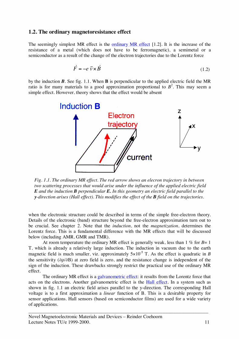
The seemingly simplest MR effect is the ordinary MR effect [1.2]. It is the increase of theresistance of a metal (which does not have to be ferromagnetic), a semimetal or asemiconductor as a result of the change of the electron trajectories due to the Lorentz force
BveF ×−= (1.2)
by the induction B. See fig. 1.1. When B is perpendicular to the applied electric field the MRratio is for many materials to a good approximation proportional to B2. This may seem asimple effect. However, theory shows that the effect would be absent
when the electronic structure could be described in terms of the simple free-electron theory.Details of the electronic (band) structure beyond the free-electron approximation turn out tobe crucial. See chapter 2. Note that the induction, not the magnetization, determines theLorentz force. This is a fundamental difference with the MR effects that will be discussedbelow (including AMR, GMR and TMR).
At room temperature the ordinary MR effect is generally weak, less than 1 % for B= 1T, which is already a relatively large induction. The induction in vacuum due to the earthmagnetic field is much smaller, viz. approximately 5×10⁻⁵ T. As the effect is quadratic in Bthe sensitivity (∂ρ/∂B) at zero field is zero, and the resistance change is independent of thesign of the induction. These drawbacks strongly restrict the practical use of the ordinary MReffect.
The ordinary MR effect is a galvanometric effect: it results from the Lorentz force thatacts on the electrons. Another galvanometric effect is the Hall effect. In a system such asshown in fig. 1.1 an electric field arises parallel to the y-direction. The corresponding Hallvoltage is to a first approximation a linear function of B. This is a desirable property forsensor applications. Hall sensors (based on semiconductor films) are used for a wide varietyof applications.
z
x
y
Fig. 1.1. The ordinary MR effect. The red arrow shows an elecron trajectory in betweentwo scattering processes that would arise under the influence of the applied electric fieldE and the induction B perpendicular E. In this geometry an electric field parallel to they-direction arises (Hall effect). This modifies the effect of the B field on the trajectories.
___________________________________________________________________Novel Magnetoelectronic Materials and Devices – Reinder CoehoornLecture Notes TU/e 1999-2000. 12
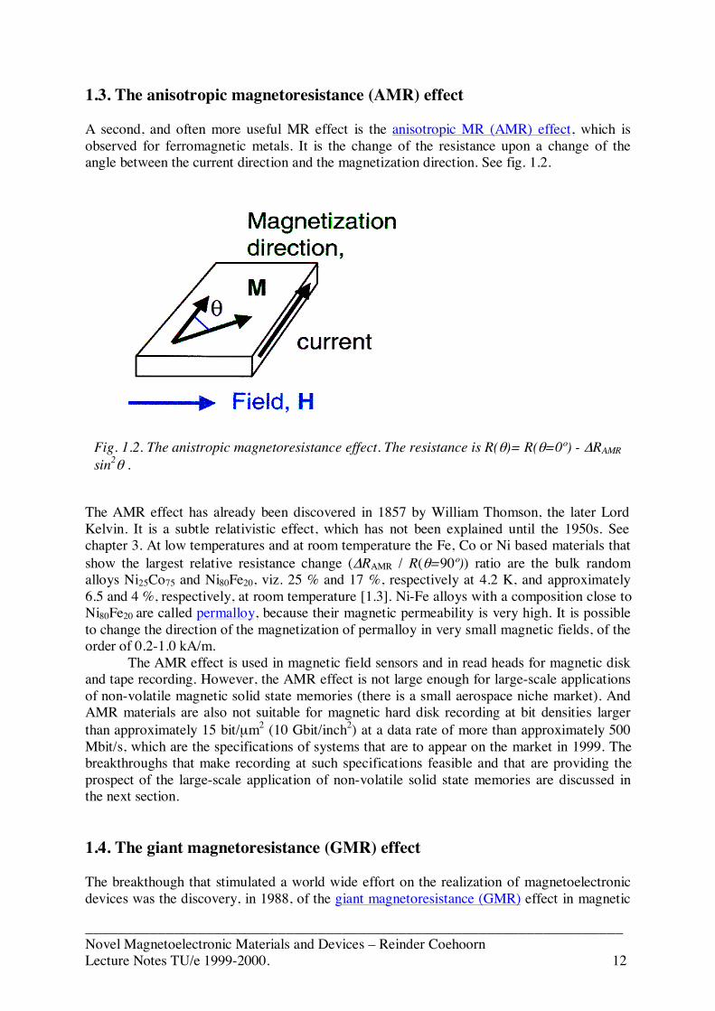
1.3. The anisotropic magnetoresistance (AMR) effect
A second, and often more useful MR effect is the anisotropic MR (AMR) effect, which isobserved for ferromagnetic metals. It is the change of the resistance upon a change of theangle between the current direction and the magnetization direction. See fig. 1.2.
The AMR effect has already been discovered in 1857 by William Thomson, the later LordKelvin. It is a subtle relativistic effect, which has not been explained until the 1950s. Seechapter 3. At low temperatures and at room temperature the Fe, Co or Ni based materials thatshow the largest relative resistance change (ΔRAMR / R(θ=90º)) ratio are the bulk randomalloys Ni25Co75 and Ni80Fe20, viz. 25 % and 17 %, respectively at 4.2 K, and approximately6.5 and 4 %, respectively, at room temperature [1.3]. Ni-Fe alloys with a composition close toNi80Fe20 are called permalloy, because their magnetic permeability is very high. It is possibleto change the direction of the magnetization of permalloy in very small magnetic fields, of theorder of 0.2-1.0 kA/m.
The AMR effect is used in magnetic field sensors and in read heads for magnetic diskand tape recording. However, the AMR effect is not large enough for large-scale applicationsof non-volatile magnetic solid state memories (there is a small aerospace niche market). AndAMR materials are also not suitable for magnetic hard disk recording at bit densities largerthan approximately 15 bit/µm2 (10 Gbit/inch2) at a data rate of more than approximately 500Mbit/s, which are the specifications of systems that are to appear on the market in 1999. Thebreakthroughs that make recording at such specifications feasible and that are providing theprospect of the large-scale application of non-volatile solid state memories are discussed inthe next section.
1.4. The giant magnetoresistance (GMR) effect
The breakthough that stimulated a world wide effort on the realization of magnetoelectronicdevices was the discovery, in 1988, of the giant magnetoresistance (GMR) effect in magnetic
Fig. 1.2. The anistropic magnetoresistance effect. The resistance is R(θ)= R(θ=0º) - ΔRAMRsin2θ .
___________________________________________________________________Novel Magnetoelectronic Materials and Devices – Reinder CoehoornLecture Notes TU/e 1999-2000. 13
multilayers. The effect was discovered independently by Albert Fert and coworkers at theUniversity of Paris-Sud [1.4] and Peter Grünberg and coworkers at the ForschungszentrumJülich [1.5].
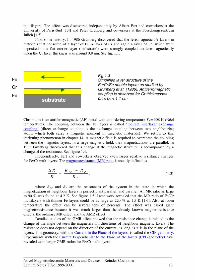
First some history. In 1986 Grünberg discovered that the ferromagnetic Fe layers inmaterials that consisted of a layer of Fe, a layer of Cr and again a layer of Fe, which weredeposited on a flat carrier layer (‘substrate’) were strongly coupled antiferromagneticallywhen the Cr layer thickness was around 0.8 nm. See fig. 1.1.
Chromium is an antiferromagnetic (AF) metal with an ordering temperature TN= 308 K (Néeltemperature). The coupling between the Fe layers is called ‘indirect interlayer exchangecoupling’ (direct exchange coupling is the exchange coupling between two neighbouringatoms which both carry a magnetic moment in magnetic materials). We return to thisintriguing phenomenon in chapter 14. A magnetic field is required to overcome the couplingbetween the magnetic layers. In a large magnetic field, their magnetizations are parallel. In1988 Grünberg discovered that this change if the magnetic structure is accompanied by achange of the resistance. See figure 1.4.
Independently, Fert and coworkers observed even larger relative resistance changesfor Fe/Cr multilayers. The magnetoresistance (MR) ratio is usually defined as
P
PAP
RRR
RR −
=Δ
, (1.3)
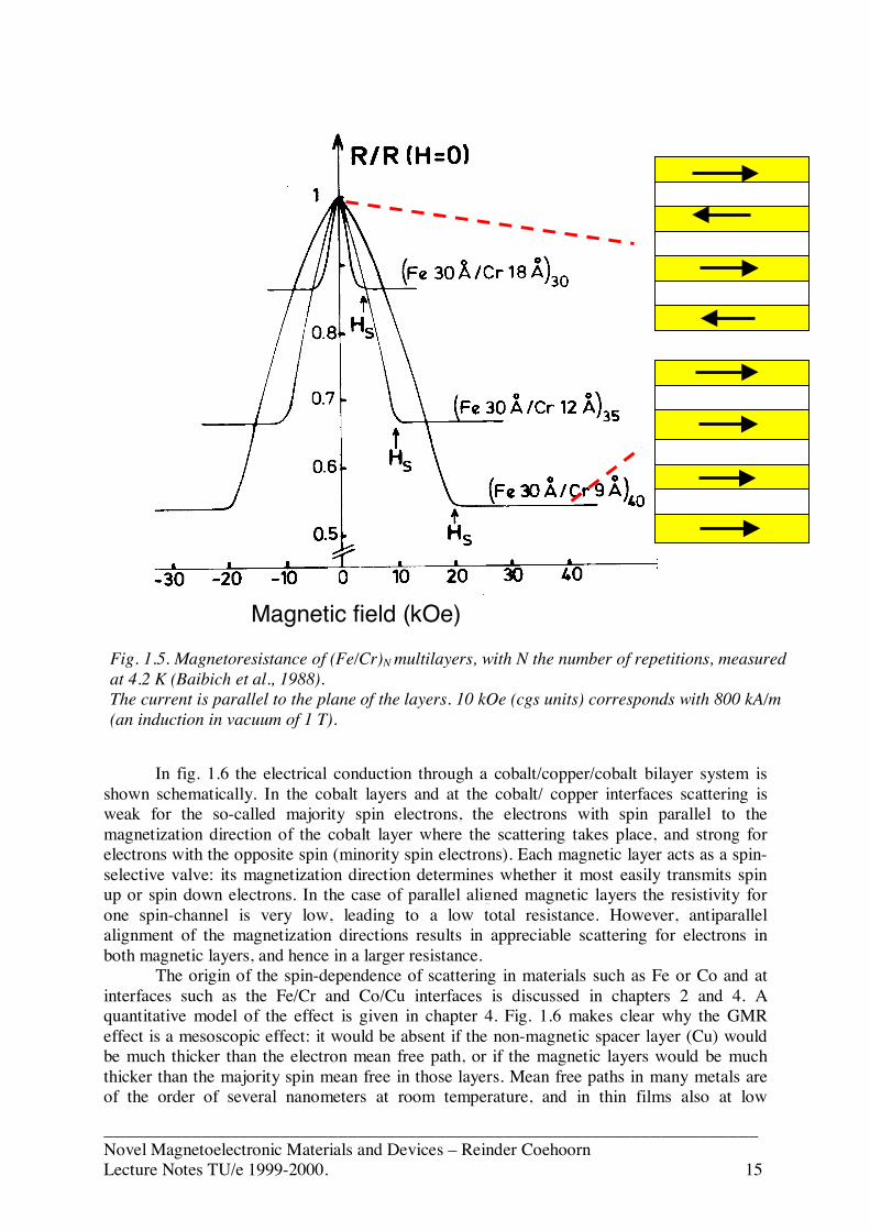
where RAP and RP are the resistances of the system in the state in which themagnetization of neighbour layers is perfectly antiparallell and parallel. An MR ratio as largeas 90 % was found at 4.2 K. See figure 1.5. Later work revealed that the MR ratio of Fe/Crmultilayers with thinner Fe layers could be as large as 220 % at 1.5 K [1.6]. Also at roomtemperature the effect can be several tens of percents. The effect was called giantmagnetoresistance because it was much larger than the already known magnetoresistanceeffects, the ordinary MR effect and the AMR effect.
Detailed studies of the GMR effect showed that the resistance change is related to thechange of the angle between the magnetization directions of neighbour magnetic layers. Theresistance does not depend on the direction of the current, as long as it is in the plane of thelayers. This geometry, with the Current In the Plane of the layers, is called the CIP-geometry.Experiments with the Current Perpendicular to the Plane of the layers (CPP-geometry) haverevealed even larger GMR ratios for Fe/Cr multilayers.
Fig.1.3Simplified layer structure of theFe/Cr/Fe double layers as studied byGrünberg et al. (1986). Antiferromagneticcoupling is observed for Cr thicknesses0.4< tCr < 1.1 nm.
FeCr
Fe substrate
___________________________________________________________________Novel Magnetoelectronic Materials and Devices – Reinder CoehoornLecture Notes TU/e 1999-2000. 14
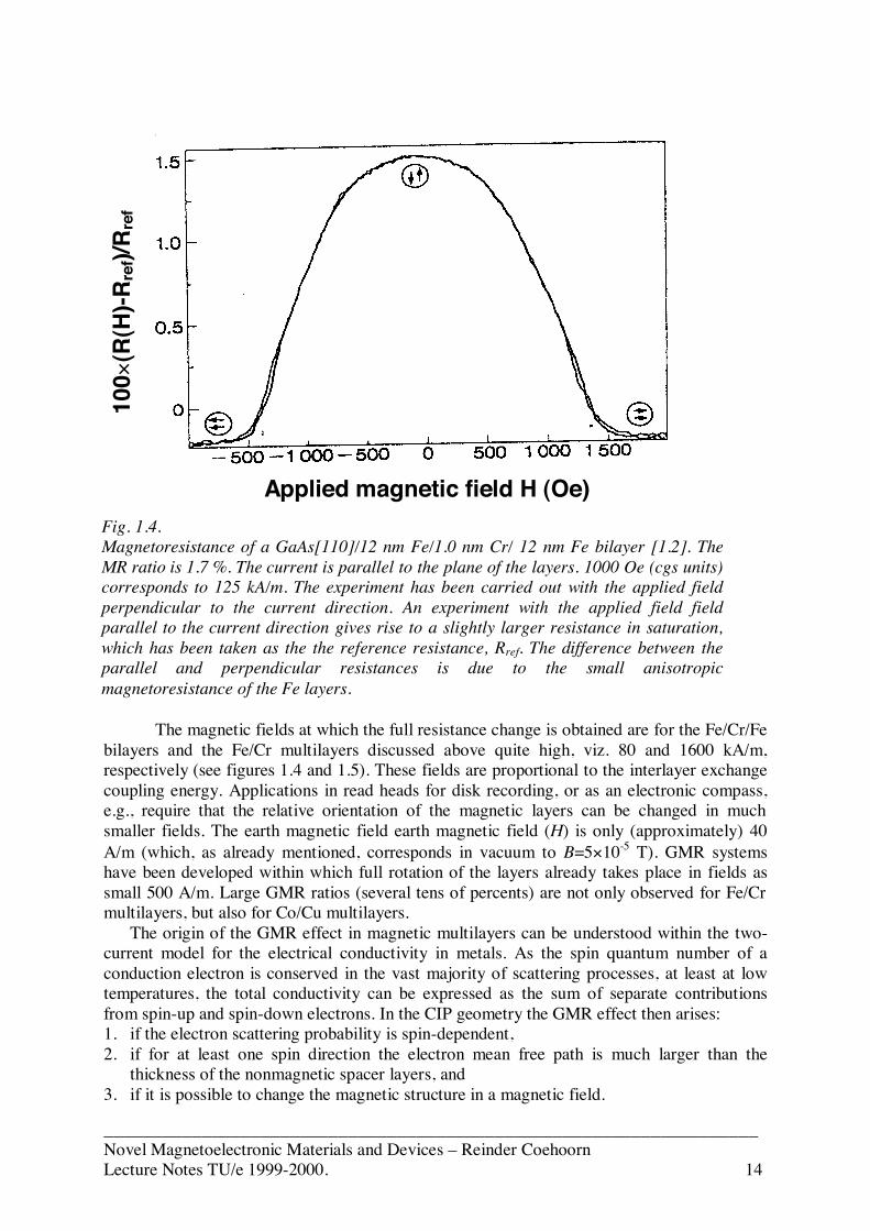
The magnetic fields at which the full resistance change is obtained are for the Fe/Cr/Febilayers and the Fe/Cr multilayers discussed above quite high, viz. 80 and 1600 kA/m,respectively (see figures 1.4 and 1.5). These fields are proportional to the interlayer exchangecoupling energy. Applications in read heads for disk recording, or as an electronic compass,e.g., require that the relative orientation of the magnetic layers can be changed in muchsmaller fields. The earth magnetic field earth magnetic field (H) is only (approximately) 40A/m (which, as already mentioned, corresponds in vacuum to B=5×10⁻⁵ T). GMR systemshave been developed within which full rotation of the layers already takes place in fields assmall 500 A/m. Large GMR ratios (several tens of percents) are not only observed for Fe/Crmultilayers, but also for Co/Cu multilayers.
The origin of the GMR effect in magnetic multilayers can be understood within the two-current model for the electrical conductivity in metals. As the spin quantum number of aconduction electron is conserved in the vast majority of scattering processes, at least at lowtemperatures, the total conductivity can be expressed as the sum of separate contributionsfrom spin-up and spin-down electrons. In the CIP geometry the GMR effect then arises:1. if the electron scattering probability is spin-dependent,2. if for at least one spin direction the electron mean free path is much larger than the
thickness of the nonmagnetic spacer layers, and3. if it is possible to change the magnetic structure in a magnetic field.
100×
(R(H
)-Rre
f)/R r
ef
Applied magnetic field H (Oe)Fig. 1.4.Magnetoresistance of a GaAs[110]/12 nm Fe/1.0 nm Cr/ 12 nm Fe bilayer [1.2]. TheMR ratio is 1.7 %. The current is parallel to the plane of the layers. 1000 Oe (cgs units)corresponds to 125 kA/m. The experiment has been carried out with the applied fieldperpendicular to the current direction. An experiment with the applied field fieldparallel to the current direction gives rise to a slightly larger resistance in saturation,which has been taken as the the reference resistance, Rref. The difference between theparallel and perpendicular resistances is due to the small anisotropicmagnetoresistance of the Fe layers.
___________________________________________________________________Novel Magnetoelectronic Materials and Devices – Reinder CoehoornLecture Notes TU/e 1999-2000. 15
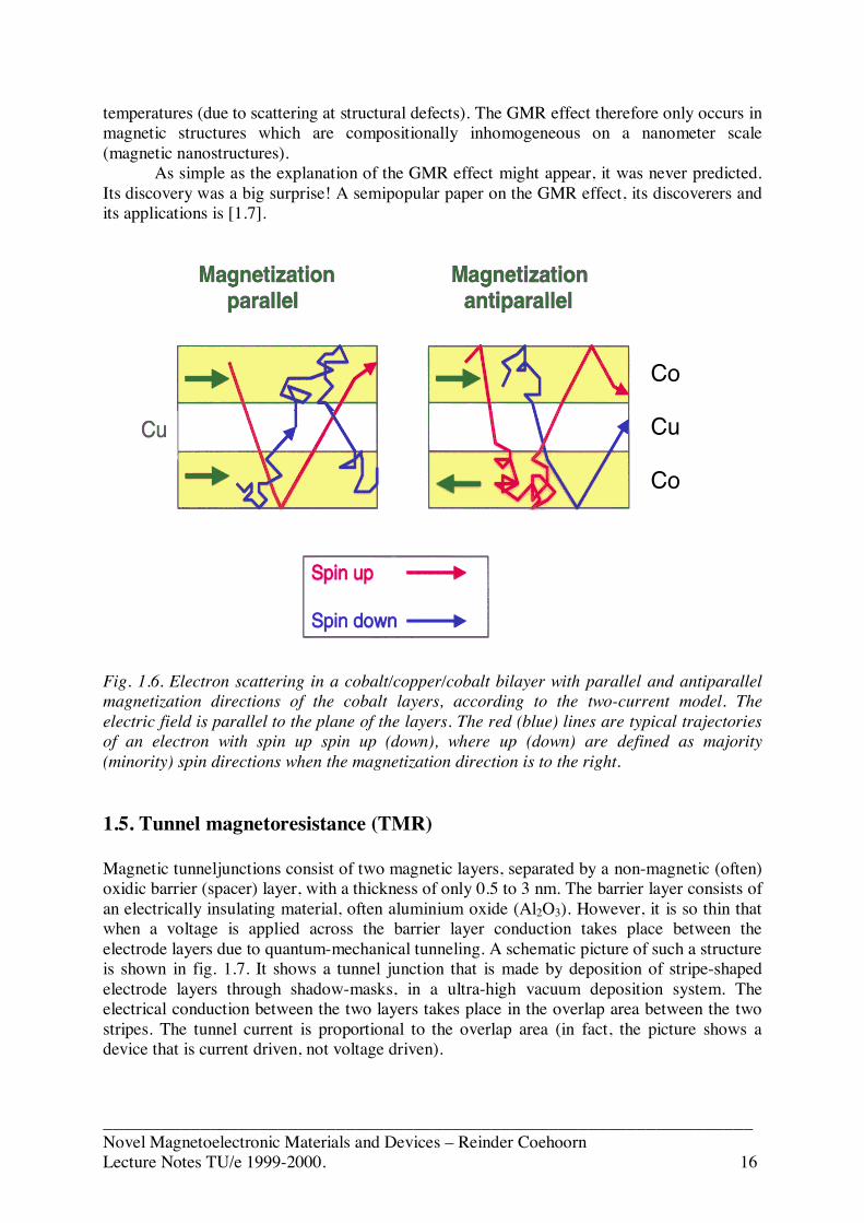
In fig. 1.6 the electrical conduction through a cobalt/copper/cobalt bilayer system isshown schematically. In the cobalt layers and at the cobalt/ copper interfaces scattering isweak for the so-called majority spin electrons, the electrons with spin parallel to themagnetization direction of the cobalt layer where the scattering takes place, and strong forelectrons with the opposite spin (minority spin electrons). Each magnetic layer acts as a spin-selective valve: its magnetization direction determines whether it most easily transmits spinup or spin down electrons. In the case of parallel aligned magnetic layers the resistivity forone spin-channel is very low, leading to a low total resistance. However, antiparallelalignment of the magnetization directions results in appreciable scattering for electrons inboth magnetic layers, and hence in a larger resistance.
The origin of the spin-dependence of scattering in materials such as Fe or Co and atinterfaces such as the Fe/Cr and Co/Cu interfaces is discussed in chapters 2 and 4. Aquantitative model of the effect is given in chapter 4. Fig. 1.6 makes clear why the GMReffect is a mesoscopic effect: it would be absent if the non-magnetic spacer layer (Cu) wouldbe much thicker than the electron mean free path, or if the magnetic layers would be muchthicker than the majority spin mean free in those layers. Mean free paths in many metals areof the order of several nanometers at room temperature, and in thin films also at low
Magnetic field (kOe)
Fig. 1.5. Magnetoresistance of (Fe/Cr)N multilayers, with N the number of repetitions, measuredat 4.2 K (Baibich et al., 1988).The current is parallel to the plane of the layers. 10 kOe (cgs units) corresponds with 800 kA/m(an induction in vacuum of 1 T).
___________________________________________________________________Novel Magnetoelectronic Materials and Devices – Reinder CoehoornLecture Notes TU/e 1999-2000. 16
temperatures (due to scattering at structural defects). The GMR effect therefore only occurs inmagnetic structures which are compositionally inhomogeneous on a nanometer scale(magnetic nanostructures).
As simple as the explanation of the GMR effect might appear, it was never predicted.Its discovery was a big surprise! A semipopular paper on the GMR effect, its discoverers andits applications is [1.7].
Fig. 1.6. Electron scattering in a cobalt/copper/cobalt bilayer with parallel and antiparallelmagnetization directions of the cobalt layers, according to the two-current model. Theelectric field is parallel to the plane of the layers. The red (blue) lines are typical trajectoriesof an electron with spin up spin up (down), where up (down) are defined as majority(minority) spin directions when the magnetization direction is to the right.
1.5. Tunnel magnetoresistance (TMR)
Magnetic tunneljunctions consist of two magnetic layers, separated by a non-magnetic (often)oxidic barrier (spacer) layer, with a thickness of only 0.5 to 3 nm. The barrier layer consists ofan electrically insulating material, often aluminium oxide (Al2O3). However, it is so thin thatwhen a voltage is applied across the barrier layer conduction takes place between theelectrode layers due to quantum-mechanical tunneling. A schematic picture of such a structureis shown in fig. 1.7. It shows a tunnel junction that is made by deposition of stripe-shapedelectrode layers through shadow-masks, in a ultra-high vacuum deposition system. Theelectrical conduction between the two layers takes place in the overlap area between the twostripes. The tunnel current is proportional to the overlap area (in fact, the picture shows adevice that is current driven, not voltage driven).
Low resistance High resistancelow
Co
Cu
Co

___________________________________________________________________Novel Magnetoelectronic Materials and Devices – Reinder CoehoornLecture Notes TU/e 1999-2000. 17
Fig. 1.7. Magnetic tunnel junction formed by two crossed stripe-shaped thin magnetic layers,separated by an oxidic barrier layer.
When the electrode layers are made of a ferromagnetic material the tunnel current depends onthe angle between the magnetization directions of the two electrode layers. This tunnelmagnetoresistance (TMR) effect (sometimes also called ‘junction magnetoresistance (JMR)effect’) is due to the dependence of the tunnel probability of electrons on their spin direction.
The TMR effect has been discovered already in 1975 [1.8]. However, only in 1995 aprocess was developed which led to junctions that showed a high TMR ratio at roomtemperature [1.9]. Nowadays magnetoresistance ratios of typically 40 % are obtained forsystems such as Co/Al2O3/Co. Magnetic tunnel junctions are considered as candidates forapplications in MRAMs, and maybe in magnetic read heads. Ref. [1.10] is an overview article(in Dutch).
1.6. Overview of novel magnetoelectronic devices
A wide variety of structures of magnetoelectronic devices has been proposed and in partrealized. Below a selection is given on the basic elements of such devices are given. Onlyschematic pictures are given, and only the ‘active part’ of the device is shown. Current leadsare indicated only schematically, although in actual devices their geometry is sometimesimportant. For the color scheme used: see overview chapter.(Although the devices discussed in this lecture series are based on continuous layers, it shouldbe remarked that in some cases interesting effects have been observed for systems withdiscontinuous layers (layers which are not uniform in the direction parallel to the film plane,but consist e.g. of ‘clusters’ or ‘islands’)).

___________________________________________________________________Novel Magnetoelectronic Materials and Devices – Reinder CoehoornLecture Notes TU/e 1999-2000. 18
1. CIP-GMR element. Device based on a magnetic metallic layered material, with thecurrent parallel to the plane of the layers. Length scales: (spin-dependent) mean freepaths.
2. CPP-GMR element. Device based on a magnetic metallic layered material, with thecurrent perpendicular to the plane of the layers. Length scale: spin diffusion length (for 5-50 nm thick films at 4.2 K typically ≈5 nm for Ni80Fe20, ≈50 nm for Co, and ≈500 nm forCu).
3. Magnetic tunnel junction. Device in which two magnetic electrode layers are separatedby a 0.5-3 nm barrier layer across which conduction takes place as a result of electrontunneling. Double junctions (with two barrier layers, and in the center of the structure anadditional magnetic or non-magnetic metallic layer) have also been proposed. Inschematic pictures of layer structures the width of the non-metallic barrier layers will belarger than the width of the metallic layers, in order to discriminate such layers frommetallic spacer layers.
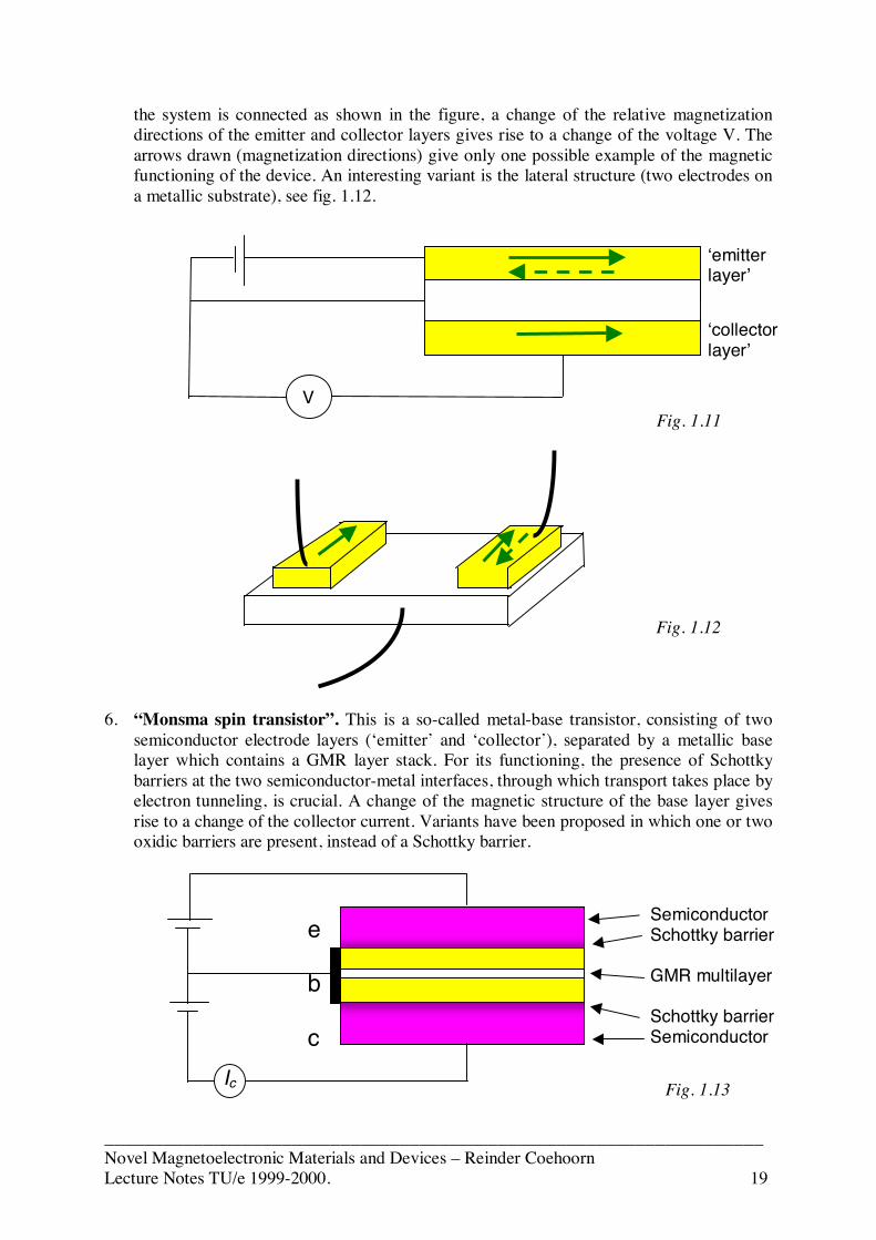
4. “Johnson spin switch” (“all metal spin transistor”). In contrast to the structures 1-3this is a three-terminal device (fig. 1.11). A ferromagnetic ‘emitter layer’ and aferromagnetic ‘collector layer’ are separated by a metallic non-ferromagnetic layer. When
current
cur
rent
oxidebarrrierlayer
Electrode layers(high sheetresistance)
curre
nt
Double junction with aferromagnetic or non-magneticmetallic central layer
Fig. 1.8
Fig. 1.9
Fig. 1.10
___________________________________________________________________Novel Magnetoelectronic Materials and Devices – Reinder CoehoornLecture Notes TU/e 1999-2000. 19
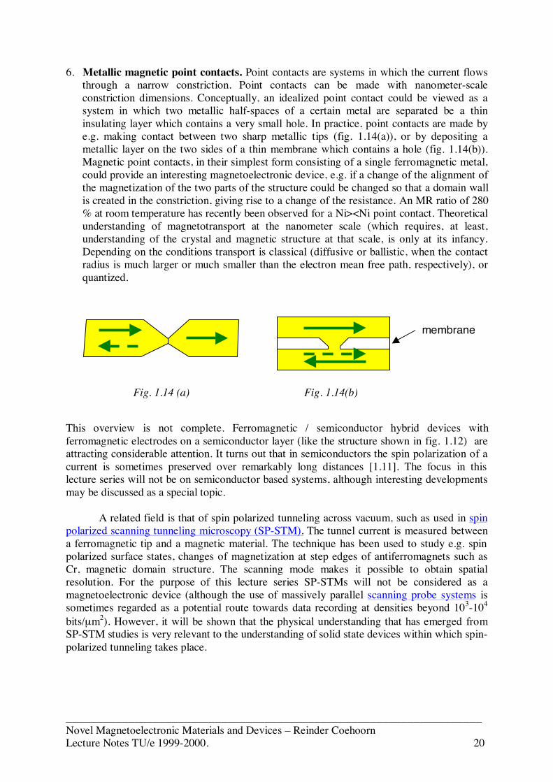
the system is connected as shown in the figure, a change of the relative magnetizationdirections of the emitter and collector layers gives rise to a change of the voltage V. Thearrows drawn (magnetization directions) give only one possible example of the magneticfunctioning of the device. An interesting variant is the lateral structure (two electrodes ona metallic substrate), see fig. 1.12.
1. 2. 3. 5.
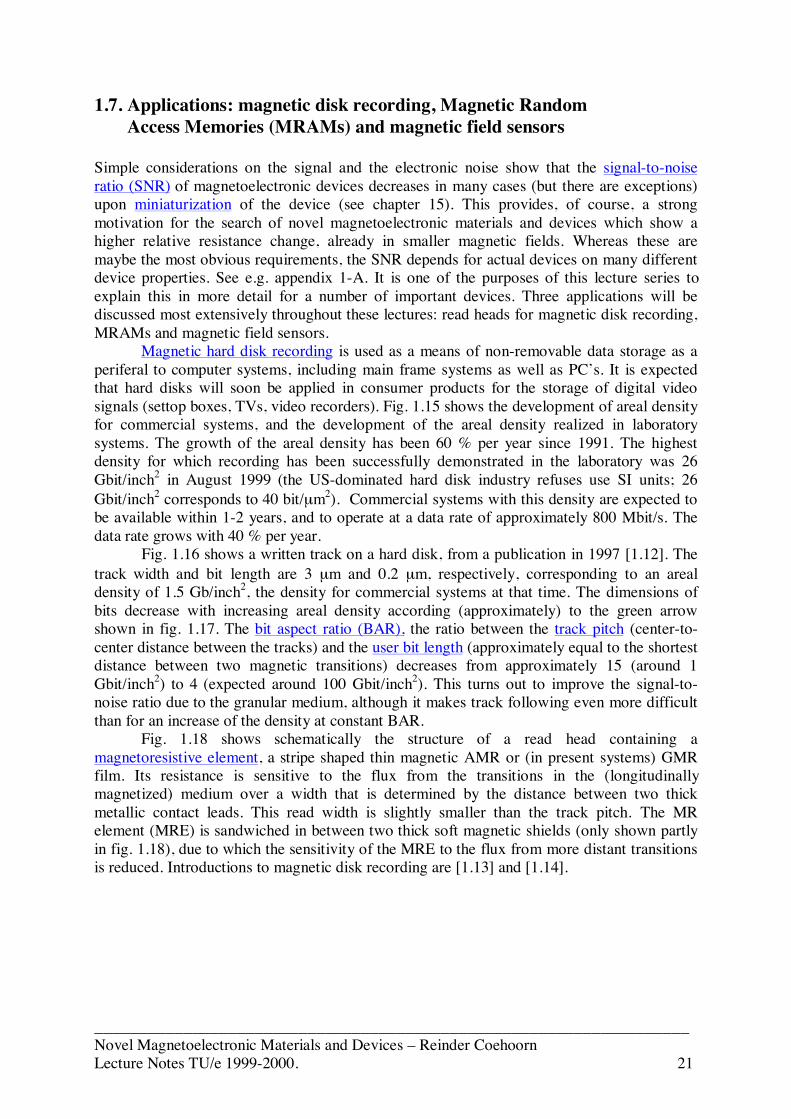
6. “Monsma spin transistor”. This is a so-called metal-base transistor, consisting of twosemiconductor electrode layers (‘emitter’ and ‘collector’), separated by a metallic baselayer which contains a GMR layer stack. For its functioning, the presence of Schottkybarriers at the two semiconductor-metal interfaces, through which transport takes place byelectron tunneling, is crucial. A change of the magnetic structure of the base layer givesrise to a change of the collector current. Variants have been proposed in which one or twooxidic barriers are present, instead of a Schottky barrier.
V
e
b
c
SemiconductorSchottky barrier
GMR multilayer
Schottky barrierSemiconductor
‘emitterlayer’
‘collectorlayer’
Fig. 1.11
Fig. 1.12
Ic Fig. 1.13
___________________________________________________________________Novel Magnetoelectronic Materials and Devices – Reinder CoehoornLecture Notes TU/e 1999-2000. 20
6. Metallic magnetic point contacts. Point contacts are systems in which the current flowsthrough a narrow constriction. Point contacts can be made with nanometer-scaleconstriction dimensions. Conceptually, an idealized point contact could be viewed as asystem in which two metallic half-spaces of a certain metal are separated be a thininsulating layer which contains a very small hole. In practice, point contacts are made bye.g. making contact between two sharp metallic tips (fig. 1.14(a)), or by depositing ametallic layer on the two sides of a thin membrane which contains a hole (fig. 1.14(b)).Magnetic point contacts, in their simplest form consisting of a single ferromagnetic metal,could provide an interesting magnetoelectronic device, e.g. if a change of the alignment ofthe magnetization of the two parts of the structure could be changed so that a domain wallis created in the constriction, giving rise to a change of the resistance. An MR ratio of 280% at room temperature has recently been observed for a Ni><Ni point contact. Theoreticalunderstanding of magnetotransport at the nanometer scale (which requires, at least,understanding of the crystal and magnetic structure at that scale, is only at its infancy.Depending on the conditions transport is classical (diffusive or ballistic, when the contactradius is much larger or much smaller than the electron mean free path, respectively), orquantized.
This overview is not complete. Ferromagnetic / semiconductor hybrid devices withferromagnetic electrodes on a semiconductor layer (like the structure shown in fig. 1.12) areattracting considerable attention. It turns out that in semiconductors the spin polarization of acurrent is sometimes preserved over remarkably long distances [1.11]. The focus in thislecture series will not be on semiconductor based systems, although interesting developmentsmay be discussed as a special topic.
A related field is that of spin polarized tunneling across vacuum, such as used in spinpolarized scanning tunneling microscopy (SP-STM). The tunnel current is measured betweena ferromagnetic tip and a magnetic material. The technique has been used to study e.g. spinpolarized surface states, changes of magnetization at step edges of antiferromagnets such asCr, magnetic domain structure. The scanning mode makes it possible to obtain spatialresolution. For the purpose of this lecture series SP-STMs will not be considered as amagnetoelectronic device (although the use of massively parallel scanning probe systems issometimes regarded as a potential route towards data recording at densities beyond 103-104
bits/µm2). However, it will be shown that the physical understanding that has emerged fromSP-STM studies is very relevant to the understanding of solid state devices within which spin-polarized tunneling takes place.
membrane
Fig. 1.14 (a) Fig. 1.14(b)
___________________________________________________________________Novel Magnetoelectronic Materials and Devices – Reinder CoehoornLecture Notes TU/e 1999-2000. 21
1.7. Applications: magnetic disk recording, Magnetic Random Access Memories (MRAMs) and magnetic field sensors
Simple considerations on the signal and the electronic noise show that the signal-to-noiseratio (SNR) of magnetoelectronic devices decreases in many cases (but there are exceptions)upon miniaturization of the device (see chapter 15). This provides, of course, a strongmotivation for the search of novel magnetoelectronic materials and devices which show ahigher relative resistance change, already in smaller magnetic fields. Whereas these aremaybe the most obvious requirements, the SNR depends for actual devices on many differentdevice properties. See e.g. appendix 1-A. It is one of the purposes of this lecture series toexplain this in more detail for a number of important devices. Three applications will bediscussed most extensively throughout these lectures: read heads for magnetic disk recording,MRAMs and magnetic field sensors.
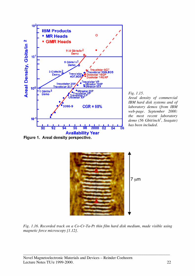
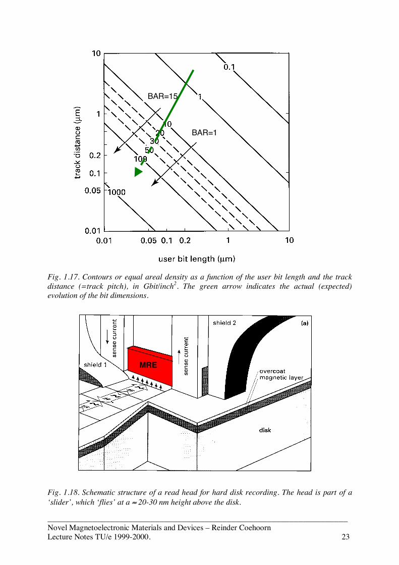
Magnetic hard disk recording is used as a means of non-removable data storage as aperiferal to computer systems, including main frame systems as well as PC’s. It is expectedthat hard disks will soon be applied in consumer products for the storage of digital videosignals (settop boxes, TVs, video recorders). Fig. 1.15 shows the development of areal densityfor commercial systems, and the development of the areal density realized in laboratorysystems. The growth of the areal density has been 60 % per year since 1991. The highestdensity for which recording has been successfully demonstrated in the laboratory was 26Gbit/inch2 in August 1999 (the US-dominated hard disk industry refuses use SI units; 26Gbit/inch2 corresponds to 40 bit/µm2). Commercial systems with this density are expected tobe available within 1-2 years, and to operate at a data rate of approximately 800 Mbit/s. Thedata rate grows with 40 % per year.
Fig. 1.16 shows a written track on a hard disk, from a publication in 1997 [1.12]. Thetrack width and bit length are 3 µm and 0.2 µm, respectively, corresponding to an arealdensity of 1.5 Gb/inch2, the density for commercial systems at that time. The dimensions ofbits decrease with increasing areal density according (approximately) to the green arrowshown in fig. 1.17. The bit aspect ratio (BAR), the ratio between the track pitch (center-to-center distance between the tracks) and the user bit length (approximately equal to the shortestdistance between two magnetic transitions) decreases from approximately 15 (around 1Gbit/inch2) to 4 (expected around 100 Gbit/inch2). This turns out to improve the signal-to-noise ratio due to the granular medium, although it makes track following even more difficultthan for an increase of the density at constant BAR.
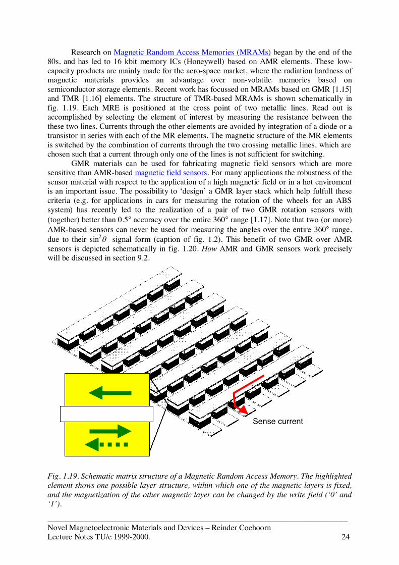
Fig. 1.18 shows schematically the structure of a read head containing amagnetoresistive element, a stripe shaped thin magnetic AMR or (in present systems) GMRfilm. Its resistance is sensitive to the flux from the transitions in the (longitudinallymagnetized) medium over a width that is determined by the distance between two thickmetallic contact leads. This read width is slightly smaller than the track pitch. The MRelement (MRE) is sandwiched in between two thick soft magnetic shields (only shown partlyin fig. 1.18), due to which the sensitivity of the MRE to the flux from more distant transitionsis reduced. Introductions to magnetic disk recording are [1.13] and [1.14].
___________________________________________________________________Novel Magnetoelectronic Materials and Devices – Reinder CoehoornLecture Notes TU/e 1999-2000. 22
Fig. 1.16. Recorded track on a Co-Cr-Ta-Pt thin film hard disk medium, made visible usingmagnetic force microscopy [1.12].
Fig. 1.15.Areal density of commercialIBM hard disk systems and oflaboratory demos (from IBMweb-page. September 2000:the most recent laboratorydemo (56 Gbit/inch2, Seagate)has been included.
°
7 µm
•
___________________________________________________________________Novel Magnetoelectronic Materials and Devices – Reinder CoehoornLecture Notes TU/e 1999-2000. 23
Fig. 1.17. Contours or equal areal density as a function of the user bit length and the trackdistance (=track pitch), in Gbit/inch2. The green arrow indicates the actual (expected)evolution of the bit dimensions.
Fig. 1.18. Schematic structure of a read head for hard disk recording. The head is part of a‘slider’, which ‘flies’ at a ≈ 20-30 nm height above the disk.
BAR=15
BAR=1
MRE
___________________________________________________________________Novel Magnetoelectronic Materials and Devices – Reinder CoehoornLecture Notes TU/e 1999-2000. 24
Research on Magnetic Random Access Memories (MRAMs) began by the end of the80s, and has led to 16 kbit memory ICs (Honeywell) based on AMR elements. These low-capacity products are mainly made for the aero-space market, where the radiation hardness ofmagnetic materials provides an advantage over non-volatile memories based onsemiconductor storage elements. Recent work has focussed on MRAMs based on GMR [1.15]and TMR [1.16] elements. The structure of TMR-based MRAMs is shown schematically infig. 1.19. Each MRE is positioned at the cross point of two metallic lines. Read out isaccomplished by selecting the element of interest by measuring the resistance between thethese two lines. Currents through the other elements are avoided by integration of a diode or atransistor in series with each of the MR elements. The magnetic structure of the MR elementsis switched by the combination of currents through the two crossing metallic lines, which arechosen such that a current through only one of the lines is not sufficient for switching.
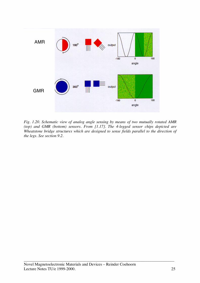
GMR materials can be used for fabricating magnetic field sensors which are moresensitive than AMR-based magnetic field sensors. For many applications the robustness of thesensor material with respect to the application of a high magnetic field or in a hot enviromentis an important issue. The possibility to ‘design’ a GMR layer stack which help fulfull thesecriteria (e.g. for applications in cars for measuring the rotation of the wheels for an ABSsystem) has recently led to the realization of a pair of two GMR rotation sensors with(together) better than 0.5° accuracy over the entire 360° range [1.17]. Note that two (or more)AMR-based sensors can never be used for measuring the angles over the entire 360° range,due to their sin2θ signal form (caption of fig. 1.2). This benefit of two GMR over AMRsensors is depicted schematically in fig. 1.20. How AMR and GMR sensors work preciselywill be discussed in section 9.2.
Fig. 1.19. Schematic matrix structure of a Magnetic Random Access Memory. The highlightedelement shows one possible layer structure, within which one of the magnetic layers is fixed,and the magnetization of the other magnetic layer can be changed by the write field (‘0’ and‘1’).
Sense current
___________________________________________________________________Novel Magnetoelectronic Materials and Devices – Reinder CoehoornLecture Notes TU/e 1999-2000. 25
Fig. 1.20. Schematic view of analog angle sensing by means of two mutually rotated AMR(top) and GMR (bottom) sensors. From [1.17]. The 4-legged sensor chips depicted areWheatstone bridge structures which are designed to sense fields parallel to the direction ofthe legs. See section 9.2.
AMR
GMR
___________________________________________________________________Novel Magnetoelectronic Materials and Devices – Reinder CoehoornLecture Notes TU/e 1999-2000. 26
Appendix 1A.Some remarks on effect of the temperature rise of magneto-electronicdevices on the output signal
The thermal conductivity of the environment of a magnetoelectronic device can be a factorwhich ultimately limits its performance. Let us consider a read head. The signal voltage VS(t),i.e. the signal-related a.c. part of the voltage across the MRE (i.e. the total voltage across theMRE minus the random noise voltage across the MRE, is equal to
))(()( avSsenseS RtRItV −= , (1A-1)
where RS(t) is the signal-related part of the time dependent resistance, Rav is the time-averageof the resistance, and Isense is the sense current through the MRE. The factors that determinethe time dependence of the resistance (including the magnetoresistance ratio, the flux from themedium and the flux efficiency of the head) are discussed in Ch. 9. These factors may beimproved by improvements of the properties of the MR material, the medium material (andthe write heads which should be able to write the signal at the required density), and themechanics (making a low stable flying heigth and good track following possible).
In addition, the signal voltage is also proportional to the sense current. Limitations ofthe maximum allowable sense current ultimately limit the performance of a given head-medium system. In the first place, the sense current leads to dissipation of power in the MRE.For battery powered portable systems this contribution to the overall power consumption mayalready limit the allowable sense current. Secondly, the sense current gives rise to a magneticfield, which acts on the magnetic layers and may influence the flux dependence of theresistance. The focus will be on a third issue, viz. the resulting temperature rise of the MREleads, which leads to a maximum of the allowed sense current. Heating of the MRE can leadto long term degradation due to thermally activated electromigration, due to degradation ofthe layer structure due to diffusion across the interfaces, or due to an irreversible change ofthe exchange biasing interaction. In addition, the MR ratio of magnetoelectronic devicesdecreases generally with increasing temperature, leading to an optimum of the signal voltageas a function of the sense current, instead of a monotonic increase. Let us, as a simpleexample, calculate the temperature rise of a thin film MRE in between two shields, each at adistance g (the read gap length) from the MRE, separated from the MRE by an insulating gapoxide with a thermal conductivity κox. Nowadays, Al2O3 is used, with for thin films κox.≈1Wm-1K-1. The shields are assumed to be perfect heat sinks, and the heat flow problem isassumed to be one-dimensional (no heat flow to the current leads). This latter approximationis in fact not quite correct, but for the purpose of the present discussion that does not present aproblem. Setting the power dissipated in the MRE per unit area equal to the heat flux to theshield leads to the following expression for the maximum allowable sense current when thetemperature rise should not exceed a value ΔT (verify this yourselves):
hgR
TIsh
os ×
Δ=
κ , (1A-2)
where h is the MRE height (i.e. the dimension of the MRE stripe in the directionperpendicular to the disk surface). Eq. (1.5) reveals the importance of improvements of thethermal conductivity of the gap material. Use of e.g. AlN, with for thin films κox.≈3 Wm-1K-1,

___________________________________________________________________Novel Magnetoelectronic Materials and Devices – Reinder CoehoornLecture Notes TU/e 1999-2000. 27
instead of Al2O3, can improve the performance of MR heads by a factor √3. Secondly, as gdecreases with decreasing user bit length, cooling to the shields becomes more efficient. Partof the ever increasing sensitivity (in terms of output voltage) of read heads, is due to thepossibility to use ever increasing current densities. The current density in GMR elements inread heads used for laboratory demonstrations is nowadays typically 5×10¹¹ A/m2, one orderof magnitude larger than the current densities typically used in interconnect lines onsemiconductor Integrated Circuits (ICs). However, due to the efficient cooling, the resultingtemperature rise in such heads can be limited to +50 K.

___________________________________________________________________Novel Magnetoelectronic Materials and Devices – Reinder CoehoornLecture Notes TU/e 1999-2000. 28
References Chapter 1
1.1 “Ultrathin Magnetic Structures”, B. Heinrich and J.A.C. Bland (eds), Vols 1 and 2,Springer-Verlag, Berlin, (1994).
1.2 J.P. Jan, Solid State Physics 5, 1-96 (1957).1.3 T.R. McGuire and R.I. Potter, IEEE Trans. Magnetics 11, 1018 (1975).1.4 G. Binasch, P. Grünberg, F. Saurenbach and W. Zinn, Phys. Rev. B 39, 4828 (1989).1.5 M.N. Baibich et al., Phys. Rev. Lett. 61, 2472 (1988).1.6 R. Schad, C.D. Potter, P. Beliën, G. Verbanck, V.V. Moschalkov and Y.
Bruynseraede, Appl. Phys. Lett. 64, 3500 (1994).1.7 M. Ross, Europhysics News 28, 114 (1997).1.8 J. Moodera et al., Phys. Rev. Lett. 74, 3273 (1995); Phys. Rev. Lett. 80, 2941 (1998).1.9 M. Julliere, Phys. Lett. 54, 225 (1975).1.10 H. Swagten en R. Coehoorn, Nederlands Tijdschrift voor Natuurkunde 64, 279 (1998).1.11 D.D. Awschalom and J.M. Kikkawa, Physics Today 52, 33 (1999).1.12 S. Malhotra et al., IEEE Trans. Magn. 33, 2882 (1997).1.13 C.D. Mee and E. Daniel, “Magnetic Recording Technology”, Mc-Graw-Hill, New
York, second edition (1996).1.14 K.G.Ashar, “Magnetic disk drive Technology, heads, media, channel, interfaces and
integration”, IEEE Press, New York (1997).1.15 S. Tehrani et al., J. Appl. Phys. 85, 5822 (1999).1.16 S.S.P. Parkin et al., J. Appl. Phys. 85, 5828 (1999).1.17 K.-M.H. Lenssen et al., Sensors and Actuators A 85, 1 (2000).
Some overview papers:
• Several articles in a special issue of Physics Today 48 (April 1995) on‘Magnetoelectronics’.
• J. De Boeck and J. Wauters, “Magnetische geheugenchips”, Natuur & Techniek 67(September 1999), 16 (in Dutch, semipopular).
• J. Daughton and J. Granley, “Giant magnetoresistance devices move in”, The IndustrialScientist 5 (June 1999), 22.
(added in 2001):• P. Grünberg, "Layered magnetic structures: history, highlights, applications", Physics
Today 54 (May 2001), p. 31.
___________________________________________________________________Novel Magnetoelectronic Materials and Devices – Reinder CoehoornLecture Notes TU/e 1999-2000. 29
2. Electrical conduction inmagnetic metals
_________________________2.1. Electronic structure of magnetic metals
2.1.1. Itinerant versus localized electron statesThe fundamental physics that underlies the properties of solids is well known (Maxwellequations, quantum mechanics and (special) relativity). However, first principles (ab initio)calculations of the ground state, transport and other (e.g. optical) properties of many-electronsystems are hampered by the impossibility to deal in an exact way with the correlated motionof the interacting electrons in the systems of interest. Electrons do not move independently,but interact with each other via the (repulsive) Coulomb force. The repulsive Coulombinteraction is, effectively, weaker between electrons of equal spin, due to the Pauli exclusionprinciple. This effectively attractive exchange interaction between electrons with the samespin leads for some solids to a (ferro)magnetic ground state, but not for all solids. Why aresome solids (ferro)magnetic, and others not? Why is (bcc) iron ferromagnetic? Moregenerally, can we predict the ground state properties of a solid? These are the properties thatonly depend on the (crystal structure and lattice parameter dependent) total energy, and on theelectron and spin density, such as:• equilibrium crystal structure,• equilibrium lattice parameters,• elastic constants,• magnetization (and its dependence on the lattice parameters),• magnetic moments (i.e. the integrated magnezation within a certain well defined region
around each of the atoms).In the first part of this chapter a theoretical approach, band structure theory, will be discussed[2.1,2.2]. The ground state properties of magnetic metals based on the 3d-transition metalatoms such as Fe, Co and Ni can be explained well on the basis of this theory. In these metalsthe electrons which are responsible for the magnetism are itinerant: their wavefunctionsextend over the crystal. The 3d-electrons, which are responsible for the magnetism oftransition metal (TM) atoms, spend only a finite time on an atom, before hopping to one of itsneighbours. Band structure theory provides a reasonably successful, but not perfectdescription of the magnetic properties of these materials, because the correlated movement ofelectrons is only taken into account in an approximate way. In order to better clarify thispoint, some attention will be paid to the magnetism of rare-earth (RE) ions, for which bandstructure theory is not applicable. The 4f electrons, which are responsible for the magnetismof RE atoms, are localized, and their electronic structure is described in terms of conceptsused in atomic theory.
Later in this chapter, band structure theory will be used as the basis of a discussion ofthe electrical conduction in magnetic metals.
___________________________________________________________________Novel Magnetoelectronic Materials and Devices – Reinder CoehoornLecture Notes TU/e 1999-2000. 30
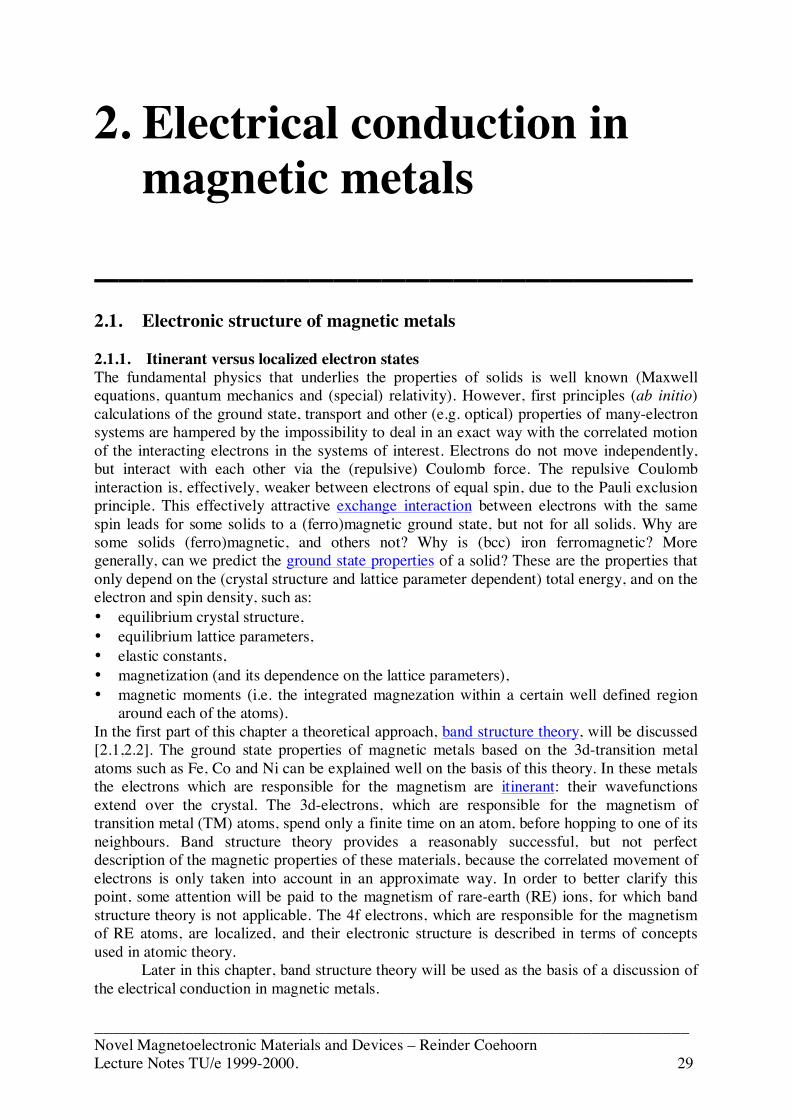
2.1.2. Formation of energy bandsWhen a molecule or a solid is formed from isolated atoms the hopping of valence electronsthrough the solid leads to modifications of the atomic energy level structure (fig. 2.1). Thesplitting, ΔE, between the states in a molecule and the band width, W, in a solid can be relatedto the time, Δt, which an itinerant electron on the average spends on an atom before hoppingto one of its neighbours. According to Heisenberg’s uncertainty principle, ΔE is of the order/Δt.
If the atomic orbitals forming a band are not completely filled, only the lower part ofthe band, up to the Fermi level EF, is occupied. In the case of a half-filled band, thecontribution per electron to the heat of formation is of the order W. The decrease of the totalenergy is mainly due to the decrease of the kinetic energy of the electrons in the occupiedlower part of the band due to the hopping process. Their wave functions have a largeramplitude in the region in between atoms than the wave functions of the states in theunoccupied upper part of the band, resulting in a less rapid spatial variation of theirwavefunction and a lower kinetic energy.
In a crystal the potential V(r) is periodic, which implies that with each eigenfunction ψa wavevector k may be associated, which is confined to the first Brillouin zone. For a given kthe solutions of the Schrödinger equation can be labeled by the band index j (usually definedsuch that Ej(k) ≤ Ej+1(k)). The set of energy levels Ej(k) with a certain value of j is called anenergy band.
Fig. 2.1. Schematic representation of energy levels in an atom, a molecule and a solid.
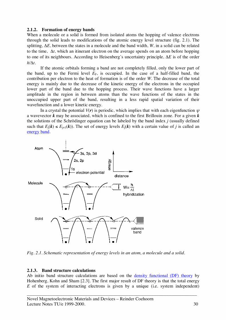
2.1.3. Band structure calculationsAb initio band structure calculations are based on the density functional (DF) theory byHohenberg, Kohn and Sham [2.3]. The first major result of DF theory is that the total energyE of the system of interacting electrons is given by a unique (i.e. system independent)
___________________________________________________________________Novel Magnetoelectronic Materials and Devices – Reinder CoehoornLecture Notes TU/e 1999-2000. 31
functional of the spin-resolved electron density throughout the system. A functional is afunction of a function. The energy functional is a function of the electron density, which is afunction of the position. Secondly, DF theory shows that the ground state charge and spindensity, which minimizes E, can be obtained by solving a set of one-electron Schrödingerequations (see below). Unfortunately, the complicated energy functional for theinhomogeneous electron gas is not known. Therefore the effective exchange-correlationcontribution to the potential which enters the one-electron Schrödinger equations is notknown. Most commonly, in practical calculations the following approximation is made. Thetotal energy E, the electron density n(r) and the spin density m(r) are obtained by solving theSchrödinger equations
)()())(2
( ,,,2
2
rErrVm sisisi
s ψψ =+∇− (2.1)
for a single electron with spin s (up or down (↑ or ↓)) in a local periodic potential which isgiven by
))(),((’)’(’
4)()(
0
2
rmrnVrr
rnrderVrV sxcext +
−+= ∫πε . (2.2)
The electron densities for spin up and spin down electrons are given by:
∑=
=sN
isi
s rrn1
2, )()( ψ , (2.3)
where N↑ and N↓ are the number of spin up and spin down eigenstates with eigenvalues Ei,s <EF. The Fermi energy, EF, is found from the condition that N↑ + N↓ = N, the total number ofelectrons. The electron and spin densities are given by n(r)= n↑(r)+ n↓(r) and m(r)= n↑(r)-n↓(r). The external potential Vext contains the attractive potential due to the nuclei, and (ifpresent) a contribution due to the external magnetic field. The second term in eq. (2.2)represents the interaction of an electron at r with the average electrostatic field due to all otherelectrons. The exchange-correlation potential Vxc
s, which depends on the spin s, is a functionof the local electron and spin density. This is an approximation, the local spin densityapproximation (LSDA), because as mentioned already in an exact treatment of the problemVxc
s(r) is a (unique) functional of the charge and spin density in the entire crystal.Within the LSDA, Vxc
s(r) is replaced by the exchange-correlation potentialVxc
s(n(r),m(r)) of the homogeneous electron gas, which is well known from numericalcalculations. The exchange-correlation term takes into account that the actual electron densityaround a certain electron at a certain point is lower than the average electron density at thatpoint, due to the direct Coulomb repulsion between electrons and the exchange interaction.The exchange interaction results from the Pauli exclusion principle, which states that the totalwavefunction of interacting electrons (fermions) is antisymmetric for the exchange of twoelectrons. This leads to a reduction of the average Coulomb repulsion between two electronswith parallel spins, compared to two electrons in similar orbitals but with antiparallel spins(see e.g. [2.1]).
The region around an electron in which the electron density is decreased as comparedto the time-averaged value is called the exchange-correlation hole. The integrated amount of‘missing’ charge corresponds to one electron charge. The radius of the exchange-correlation
___________________________________________________________________Novel Magnetoelectronic Materials and Devices – Reinder CoehoornLecture Notes TU/e 1999-2000. 32
hole at position r (taking for simplicity the case of a non-magnetic solid) is therefore of theorder of the so-called Seitz-radius, which is the radius of a sphere whose volume is equal tothe volume per conduction electron:
3/1
)(1
43
⎟⎟⎠
⎞⎜⎜⎝
⎛=
rnrs π
. (2.4)
Note that the inverse proportionality with n1/3 follows already from a dimensional analysis.Similarly, the Fermi wavelength for a homogeneous electron gas with density n is inverselyproportional with n1/3, viz. λF= (2π / [3π2n] )1/3. The size of the exchange-correlation hole istherefore proportional with the Fermi wavelength, and of the same order of magnitude. A first(order-of-magnitude) estimate of the exchange-correlation potential is therefore
3/1
041 n
reVs
xc ∝≅πε
. (2.5)
Numerical calculations for the homogeneous electron gas have revealed that for relativelylarge electron densities Vxc is indeed inversely proportional to n1/3, with a proportionalityconstant that is close to the value indicated by eq. (2.5). For small densities Vxc is a morecomplicated function of the density.
The exchange-correlation term is different for spin-up and spin-down electrons.Vxc
↑(n(r),m(r)) and Vxc↓(n(r),m(r)) become more negative with increasing charge density and
become more negative and less negative, respectively, when increasing the spin polarization.In section 2.2 the circumstances which lead to the spontaneous formation of magneticmoments are discussed.
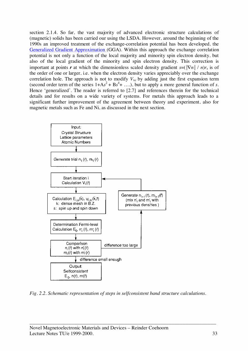
Band structure calculations are often carried out according to the scheme shown in fig.2.2. One begins by assuming a certain trial charge and spin density, from which the potentialis constructed. Then eq. (2.1) is solved for both spin directions and for a dense mesh of kpoints in the Brillouin zone (technical detail: only the ‘irreducible part of the Brillouin zone(BZ)’ has to be considered, see books on space group theory). From the wave functions of theN states with the lowest eigenvalues Ei(k) new charge and spin densities are constructed,using eq. (2.3). The procedure is repeated until selfconsistency is obtained. The old and newpotential are mixed in order to damp oscillations, thereby accelerating the convergence of theiteration process.
Within state-of-the-art methods the selfconsistent potential can have any shape. Onespeaks about full potential calculations. However, such calculations are limited with respect tothe size (number of atoms) of the unit cell. For densely packed metals a good balance betweenthe computational effort and the reliability of the results is obtained when using the AtomicSpheres Approximation (ASA), developed by the end of the 1970s [2.4], within which thecrystal is subdivided by overlapping spherical regions, centered around the atomic positions.The potential inside the spheres is taken to be spherically symetric (but the resultingselfconsistent charge and spin density is not). The ASA is used within the frequently used‘Linearized Muffin Tin Orbitals’ (LMTO) [2.5] and ‘Augmented Spherical Wave’ [2.6]methods.
The calculated ground state properties of transition metals and their compounds,obtained using the LSDA approximation, are often in a remarkably good agreement withexperiment. However, in some cases the agreement with experiment is not fully satisfactory.For Fe, Co, and Ni, e.g., the calculated lattice parameters are a few percent too small. See
___________________________________________________________________Novel Magnetoelectronic Materials and Devices – Reinder CoehoornLecture Notes TU/e 1999-2000. 33
section 2.1.4. So far, the vast majority of advanced electronic structure calculations of(magnetic) solids has been carried our using the LSDA. However, around the beginning of the1990s an improved treatment of the exchange-correlation potential has been developed, theGeneralized Gradient Approximation (GGA). Within this approach the exchange correlationpotential is not only a function of the local majority and minority spin electron density, butalso of the local gradient of the minority and spin electron density. This correction isimportant at points r at which the dimensionless scaled density gradient s=(⎥∇n⎥ / n)rs is ofthe order of one or larger, i.e. when the electron density varies appreciably over the exchangecorrelation hole. The approach is not to modify Vxc by adding just the first expansion term(second order term of the series 1+As2 + Bs4+ ….), but to apply a more general function of s.Hence ‘generalized’. The reader is referred to [2.7] and references therein for the technicaldetails and for results on a wide variety of systems. For metals this approach leads to asignificant further improvement of the agreement between theory and experiment, also formagnetic metals such as Fe and Ni, as discussed in the next section.
Fig. 2.2. Schematic representation of steps in selfconsistent band structure calculations.
___________________________________________________________________Novel Magnetoelectronic Materials and Devices – Reinder CoehoornLecture Notes TU/e 1999-2000. 34
2.1.4. Band structure calculations – ground state properties of Fe, Ni and some non-magnetic metals
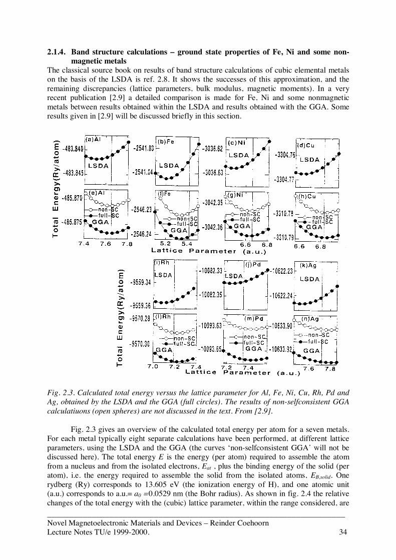
The classical source book on results of band structure calculations of cubic elemental metalson the basis of the LSDA is ref. 2.8. It shows the successes of this approximation, and theremaining discrepancies (lattice parameters, bulk modulus, magnetic moments). In a veryrecent publication [2.9] a detailed comparison is made for Fe, Ni and some nonmagneticmetals between results obtained within the LSDA and results obtained with the GGA. Someresults given in [2.9] will be discussed briefly in this section.
Fig. 2.3. Calculated total energy versus the lattice parameter for Al, Fe, Ni, Cu, Rh, Pd andAg, obtained by the LSDA and the GGA (full circles). The results of non-selfconsistent GGAcalculatiuons (open spheres) are not discussed in the text. From [2.9].
Fig. 2.3 gives an overview of the calculated total energy per atom for a seven metals.For each metal typically eight separate calculations have been performed, at different latticeparameters, using the LSDA and the GGA (the curves ‘non-selfconsistent GGA’ will not bediscussed here). The total energy E is the energy (per atom) required to assemble the atomfrom a nucleus and from the isolated electrons, Eat , plus the binding energy of the solid (peratom), i.e. the energy required to assemble the solid from the isolated atoms, EB,solid. Onerydberg (Ry) corresponds to 13.605 eV (the ionization energy of H), and one atomic unit(a.u.) corresponds to a.u.= a0 =0.0529 nm (the Bohr radius). As shown in fig. 2.4 the relativechanges of the total energy with the (cubic) lattice parameter, within the range considered, are
___________________________________________________________________Novel Magnetoelectronic Materials and Devices – Reinder CoehoornLecture Notes TU/e 1999-2000. 35
small, of the order of 0.1 eV. The predicted lattice parameter is the value at which the totalenergy is minimal.
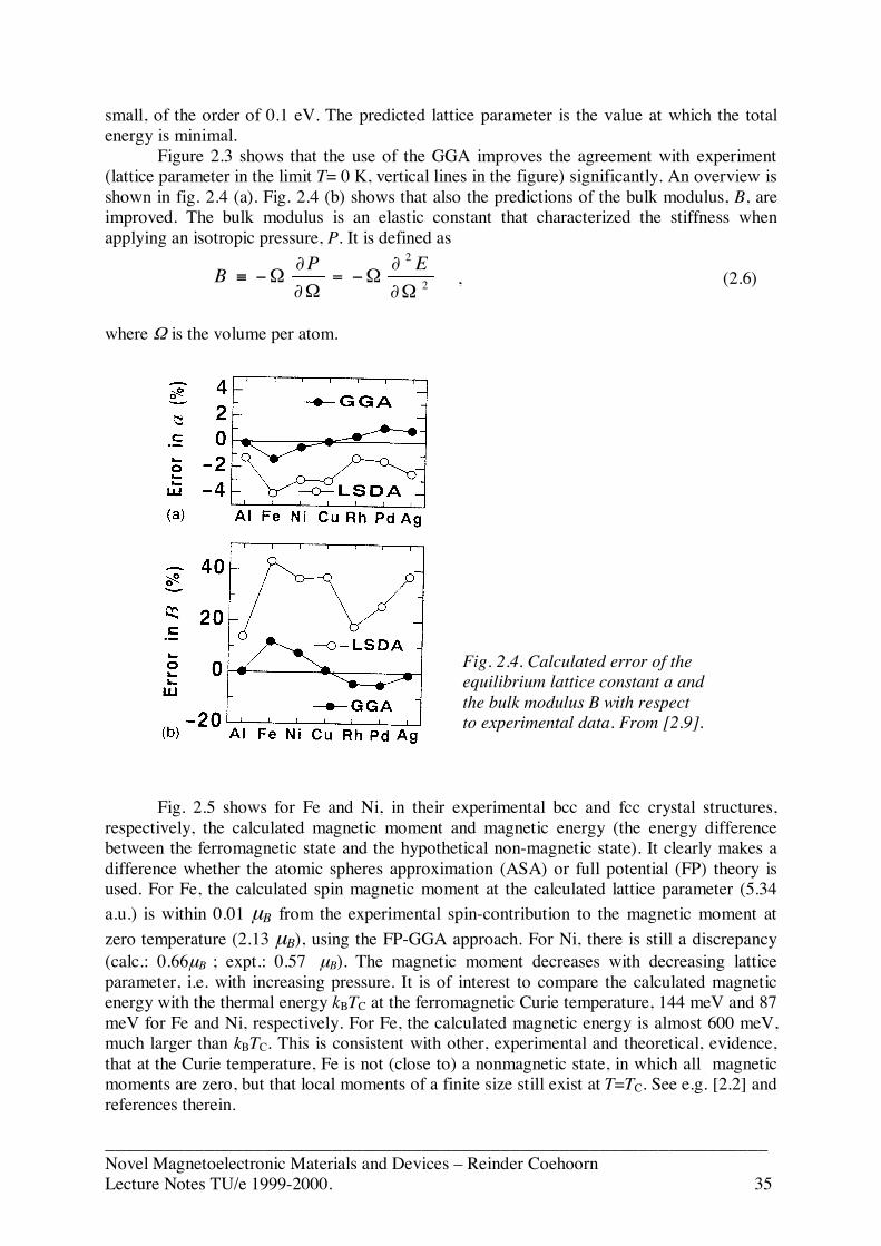
Figure 2.3 shows that the use of the GGA improves the agreement with experiment(lattice parameter in the limit T= 0 K, vertical lines in the figure) significantly. An overview isshown in fig. 2.4 (a). Fig. 2.4 (b) shows that also the predictions of the bulk modulus, B, areimproved. The bulk modulus is an elastic constant that characterized the stiffness whenapplying an isotropic pressure, P. It is defined as
2
2
Ω∂
∂Ω−=
Ω∂
∂Ω−≡
EPB , (2.6)
where Ω is the volume per atom.
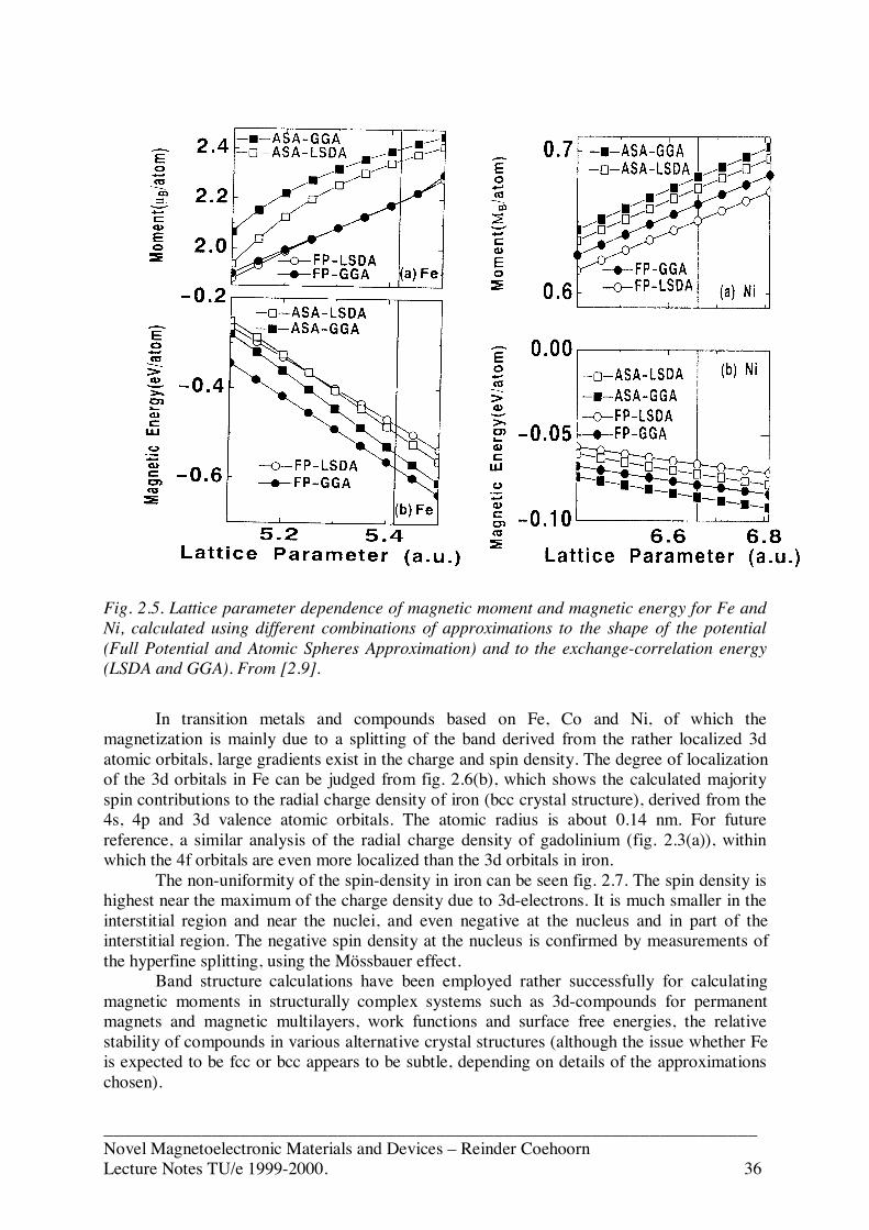
Fig. 2.5 shows for Fe and Ni, in their experimental bcc and fcc crystal structures,respectively, the calculated magnetic moment and magnetic energy (the energy differencebetween the ferromagnetic state and the hypothetical non-magnetic state). It clearly makes adifference whether the atomic spheres approximation (ASA) or full potential (FP) theory isused. For Fe, the calculated spin magnetic moment at the calculated lattice parameter (5.34a.u.) is within 0.01 µB from the experimental spin-contribution to the magnetic moment atzero temperature (2.13 µB), using the FP-GGA approach. For Ni, there is still a discrepancy(calc.: 0.66µB ; expt.: 0.57 µB). The magnetic moment decreases with decreasing latticeparameter, i.e. with increasing pressure. It is of interest to compare the calculated magneticenergy with the thermal energy kBTC at the ferromagnetic Curie temperature, 144 meV and 87meV for Fe and Ni, respectively. For Fe, the calculated magnetic energy is almost 600 meV,much larger than kBTC. This is consistent with other, experimental and theoretical, evidence,that at the Curie temperature, Fe is not (close to) a nonmagnetic state, in which all magneticmoments are zero, but that local moments of a finite size still exist at T=TC. See e.g. [2.2] andreferences therein.
Fig. 2.4. Calculated error of theequilibrium lattice constant a andthe bulk modulus B with respectto experimental data. From [2.9].
___________________________________________________________________Novel Magnetoelectronic Materials and Devices – Reinder CoehoornLecture Notes TU/e 1999-2000. 36
Fig. 2.5. Lattice parameter dependence of magnetic moment and magnetic energy for Fe andNi, calculated using different combinations of approximations to the shape of the potential(Full Potential and Atomic Spheres Approximation) and to the exchange-correlation energy(LSDA and GGA). From [2.9].
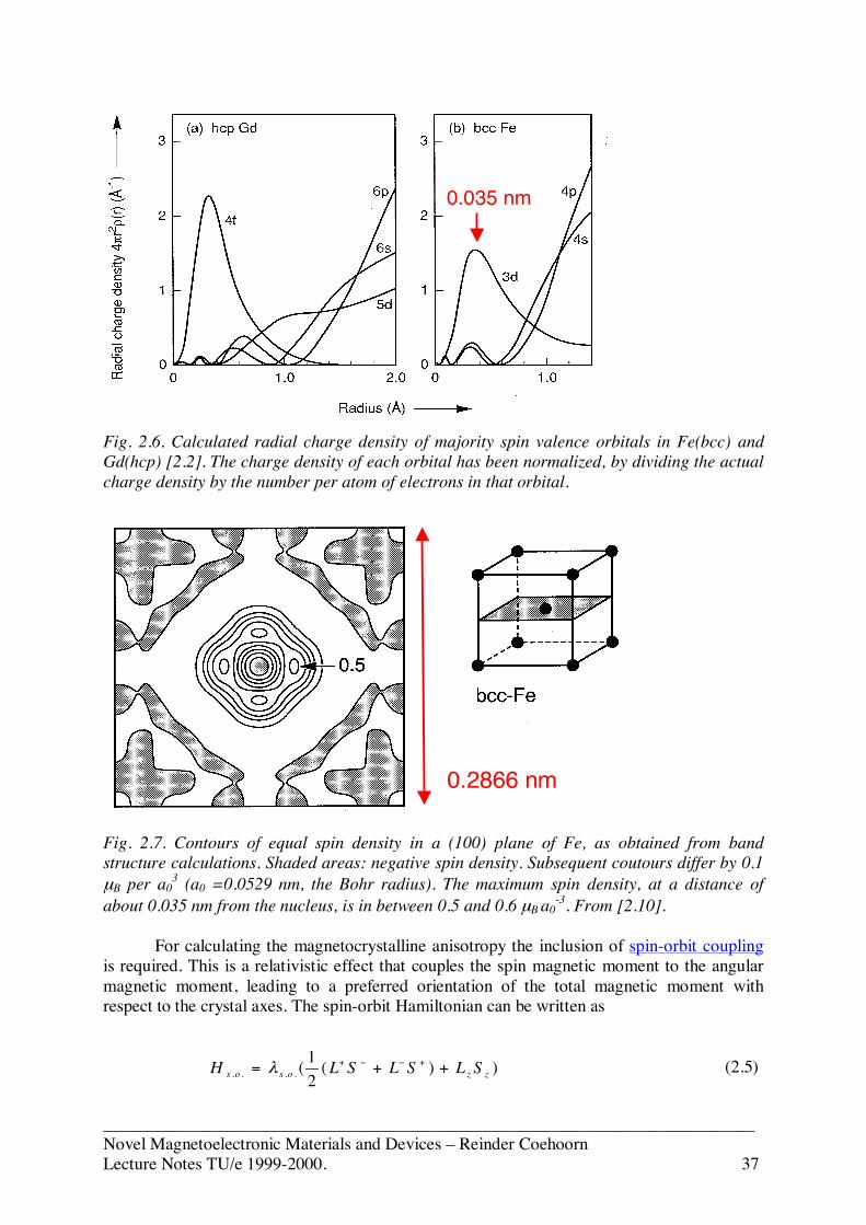
In transition metals and compounds based on Fe, Co and Ni, of which themagnetization is mainly due to a splitting of the band derived from the rather localized 3datomic orbitals, large gradients exist in the charge and spin density. The degree of localizationof the 3d orbitals in Fe can be judged from fig. 2.6(b), which shows the calculated majorityspin contributions to the radial charge density of iron (bcc crystal structure), derived from the4s, 4p and 3d valence atomic orbitals. The atomic radius is about 0.14 nm. For futurereference, a similar analysis of the radial charge density of gadolinium (fig. 2.3(a)), withinwhich the 4f orbitals are even more localized than the 3d orbitals in iron.
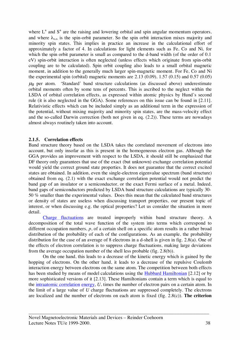
The non-uniformity of the spin-density in iron can be seen fig. 2.7. The spin density ishighest near the maximum of the charge density due to 3d-electrons. It is much smaller in theinterstitial region and near the nuclei, and even negative at the nucleus and in part of theinterstitial region. The negative spin density at the nucleus is confirmed by measurements ofthe hyperfine splitting, using the Mössbauer effect.
Band structure calculations have been employed rather successfully for calculatingmagnetic moments in structurally complex systems such as 3d-compounds for permanentmagnets and magnetic multilayers, work functions and surface free energies, the relativestability of compounds in various alternative crystal structures (although the issue whether Feis expected to be fcc or bcc appears to be subtle, depending on details of the approximationschosen).
___________________________________________________________________Novel Magnetoelectronic Materials and Devices – Reinder CoehoornLecture Notes TU/e 1999-2000. 37
Fig. 2.6. Calculated radial charge density of majority spin valence orbitals in Fe(bcc) andGd(hcp) [2.2]. The charge density of each orbital has been normalized, by dividing the actualcharge density by the number per atom of electrons in that orbital.
Fig. 2.7. Contours of equal spin density in a (100) plane of Fe, as obtained from bandstructure calculations. Shaded areas: negative spin density. Subsequent coutours differ by 0.1µB per a0
3 (a0 =0.0529 nm, the Bohr radius). The maximum spin density, at a distance ofabout 0.035 nm from the nucleus, is in between 0.5 and 0.6 µB a0
-3. From [2.10].
For calculating the magnetocrystalline anisotropy the inclusion of spin-orbit couplingis required. This is a relativistic effect that couples the spin magnetic moment to the angularmagnetic moment, leading to a preferred orientation of the total magnetic moment withrespect to the crystal axes. The spin-orbit Hamiltonian can be written as
))(21(.... zzosos SLSLSLH ++= +−−+λ (2.5)
0.2866 nm
0.035 nm
___________________________________________________________________Novel Magnetoelectronic Materials and Devices – Reinder CoehoornLecture Notes TU/e 1999-2000. 38
where L± and S± are the raising and lowering orbital and spin angular momentum operators,and where λs.o. is the spin-orbit parameter. So the spin orbit interaction mixes majority andminority spin states. This implies in practice an increase in the calculational effort ofapproximately a factor of 4. In calculations for light elements such as Fe, Co and Ni, forwhich the spin orbit parameter is small as compared to the d-band width (of the order of 0.1eV) spin-orbit interaction is often neglected (unless effects which originate from spin-orbitcoupling are to be calculated). Spin orbit coupling also leads to a small orbital magneticmoment, in addition to the generally much larger spin-magnetic moment. For Fe, Co and Nithe experimental spin (orbital) magnetic moments are 2.13 (0.09), 1.57 (0.15) and 0.57 (0.05)µB per atom. ‘Standard’ band structure calculations (as discussed above) underestimateorbital moments often by some tens of percents. This is ascribed to the neglect within theLSDA of orbital correlation effects, as expressed within atomic physics by Hund’s secondrule (it is also neglected in the GGA). Some references on this issue can be found in [2.11].Relativistic effects which can be included simply as an additional term in the expression ofthe potential, without mixing majority and minority spin states, are the mass-velocity effectand the so-called Darwin correction (both not given in eq. (2.2)). These terms are nowadaysalmost always routinely taken into account.
2.1.5. Correlation effectsBand structure theory based on the LSDA takes the correlated movement of electrons intoaccount, but only insofar as this is present in the homogeneous electron gas. Although theGGA provides an improvement with respect to the LSDA, it should still be emphasized thatDF theory only guarantees that use of the exact (but unknown) exchange correlation potentialwould yield the correct ground state properties. It does not guarantee that the correct excitedstates are obtained. In addition, even the single-electron eigenvalue spectrum (band structure)obtained from eq. (2.1) with the exact exchange correlation potential would not predict theband gap of an insulator or a semiconductor, or the exact Fermi surface of a metal. Indeed,band gaps of semiconductors predicted by LSDA band structure calculations are typically 30-50 % smaller than the experimental values. Does this mean that the calculated band structuresor density of states are useless when discussing transport properties, our present topic ofinterest, or when discussing e.g. the optical properties? Let us consider the situation in moredetail.
Charge fluctuations are treated improperly within band structure theory. Adecomposition of the total wave function of the system into terms which correspond todifferent occupation numbers, p, of a certain shell on a specific atom results in a rather broaddistribution of the probability of each of the configurations. As an example, the probabilitydistribution for the case of an average of 8 electrons in a d-shell is given in fig. 2.8(a). One ofthe effects of electron correlation is to suppress charge fluctuations, making large deviationsfrom the average occupation number of the shell less probable (fig. 2.8(b)).
On the one hand, this leads to a decrease of the kinetic energy which is gained by thehopping of electrons. On the other hand, it leads to a decrease of the repulsive Coulombinteraction energy between electrons on the same atom. The competition between both effectshas been studied by means of model calculations using the Hubbard Hamiltonian [2.12] or bymore sophisticated versions of it [2.13]. These Hamiltonians contain a term which is equal tothe intraatomic correlation energy, U, times the number of electron pairs on a certain atom. Inthe limit of a large value of U charge fluctuations are suppressed completely. The electronsare localized and the number of electrons on each atom is fixed (fig. 2.8(c)). The criterion

___________________________________________________________________Novel Magnetoelectronic Materials and Devices – Reinder CoehoornLecture Notes TU/e 1999-2000. 39
for localization is that U should be much larger than the band width W, as can be seenfrom the following quantitative discussion.
Let us consider the process of hopping of an electron between two atoms which are inthe ground state, with q electrons in the 3d shell:
2 × (3dq) 3dq-1+ 3dq+1 . (2.6)
Upon hopping q electron pairs are broken and (q+1) electron pairs are formed, and theincrease of the total energy of the system is U. The band width W is a good measure for theenergy that is gained by hopping. So U and W are the quantities that have to be compared, inorder to decide whether localization will take place.
Fig. 2.8. Schematic probability distribution of the number of d electrons on a transition metalatom. The average occupation number is 8. (a) Itinerant electrons, (b) Intermediate case, (c)Localized electrons.
The band width W is related to the overlap between orbitals on nearest neighbouratoms. Fig. 2.6 shows the radial charge densities of different orbitals in Gd and Fe metals. Thecase of rare earth metals will be discussed in order to be able to more clearly elucidate theconsequences of localization. The 4s and 4p orbitals of Fe, and the 6s, 6p and 5d orbitals ofGd have a large density at a distance from the nucleus that corresponds to the Wigner Seitzradius of the atom, i.e. the radius of a sphere with a volume equal to the volume per atom inthe solid (about 0.14 and 0.20 nm for Fe and Gd, respectively). The overlap between similarorbitals on neigbour atoms is large, resulting in broad sp and spd conduction bands,respectively. On the other hand, the 3d and, in particular, the 4f wave functions are morelocalized inside the Wigner-Seitz cell. This results in narrow 3d and 4f bands: for bcc FeW(3d)= 6.0 eV, and for hcp Gd W(4f)=0.3 eV. The variation of the calculated 3d band widthof the elemental 3d metals is shown in fig. 2.9. Towards the end of the series, the spatiallocalization of 3d orbitals increases, resulting in a decrease of the band width. Calculations of4f band widths in rare earth metals [2.14] have shown that W decreases from 1.0 eV for La, to0.2 eV for Lu. See fig. 2.10.
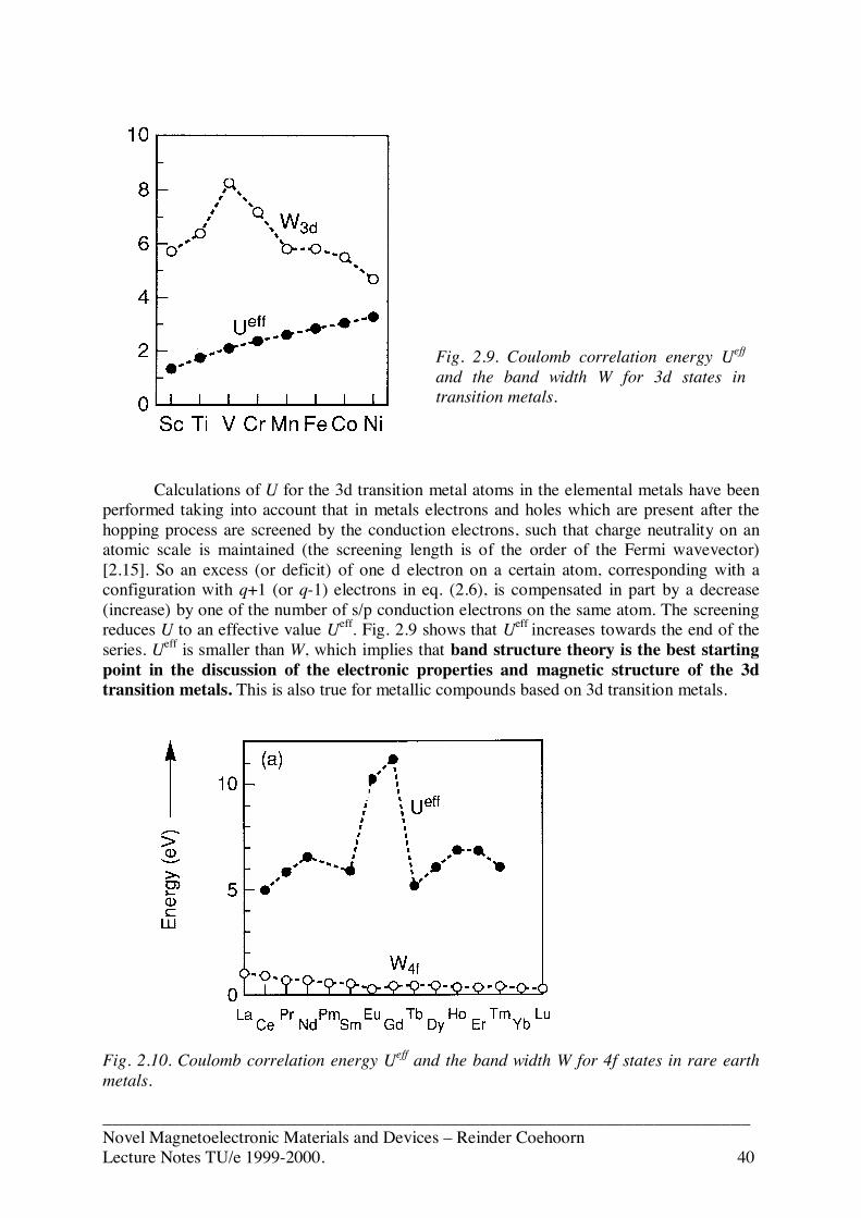
___________________________________________________________________Novel Magnetoelectronic Materials and Devices – Reinder CoehoornLecture Notes TU/e 1999-2000. 40
Calculations of U for the 3d transition metal atoms in the elemental metals have beenperformed taking into account that in metals electrons and holes which are present after thehopping process are screened by the conduction electrons, such that charge neutrality on anatomic scale is maintained (the screening length is of the order of the Fermi wavevector)[2.15]. So an excess (or deficit) of one d electron on a certain atom, corresponding with aconfiguration with q+1 (or q-1) electrons in eq. (2.6), is compensated in part by a decrease(increase) by one of the number of s/p conduction electrons on the same atom. The screeningreduces U to an effective value Ueff. Fig. 2.9 shows that Ueff increases towards the end of theseries. Ueff is smaller than W, which implies that band structure theory is the best startingpoint in the discussion of the electronic properties and magnetic structure of the 3dtransition metals. This is also true for metallic compounds based on 3d transition metals.
Fig. 2.10. Coulomb correlation energy Ueff and the band width W for 4f states in rare earthmetals.
Fig. 2.9. Coulomb correlation energy Ueff
and the band width W for 3d states intransition metals.

___________________________________________________________________Novel Magnetoelectronic Materials and Devices – Reinder CoehoornLecture Notes TU/e 1999-2000. 41
Results of calculations of Ueff for the rare earth metals are included in fig. 2.10 [2.16].In addition to the (screened) Coulomb repulsion between electrons on the same atom also theexchange interaction between electrons on the same atom with parallel spins was taken intoaccount. This interaction was neglected in the results displayed in fig. 2.9 for the 3d metals.For all 4f metals Ueff is much larger than W. Therefore, electrons in 4f shells are completelylocalized. Band structure theory is inappropriate for 4f states. One must use atomictheory, within which the magnetic properties follow from the Hund’s rules. One consequenceis that, even in cases in which calculated band structures reveal a 4f-derived density of statesat the Fermi level, 4f states do not contribute to the conduction. (It is noted that the situation issometimes slightly more complicated, viz. when a rare earth atom shows fluctuations betweentwo configurations.). A discussion of the variation of Ueff across the series of rare earth atomsis beyond the scope of this lecture series. See [2.2] and references therein.
2.1.6. Calculated band structures and densities of statesCalculated spin-polarized densities of states (DOS) for the magnetic metals Fe (bcc), Co (hcp)and Ni(fcc), and of the nonmagnetic metal Cu (fcc) are shown in fig. 2.11. It is obtained froma selfconsisten calculation of the energy eigenvalues in a dense mesh of points within theBrillouin zone. The energy is with respect to the Fermi level. The numbers of majority andminority spin electrons per atom, nmaj and nmin, follow by integrating the density of states peratom from the bottom of the valence band (at around –10 eV) to the Fermi level. Themagnetic moment m (in Bohr magneton, µB) is equal m = nmaj -nmin.
Fig. 2.11. Calculated densities of states for Fe, Co, Ni and Cu [2.2].
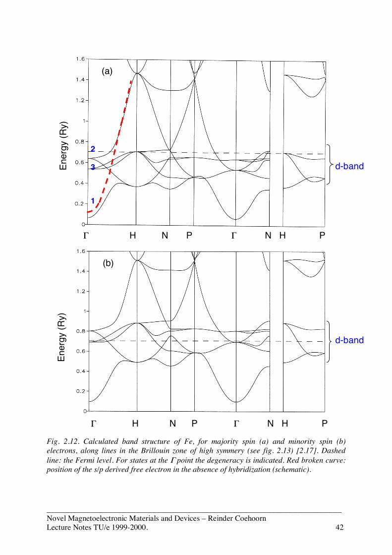
___________________________________________________________________Novel Magnetoelectronic Materials and Devices – Reinder CoehoornLecture Notes TU/e 1999-2000. 42
Fig. 2.12. Calculated band structure of Fe, for majority spin (a) and minority spin (b)electrons, along lines in the Brillouin zone of high symmery (see fig. 2.13) [2.17]. Dashedline: the Fermi level. For states at the Γ point the degeneracy is indicated. Red broken curve:position of the s/p derived free electron in the absence of hybridization (schematic).
Ener
gy (R
y)En
ergy
(Ry)
Γ H N P Γ N H P
Γ H N P Γ N H P
(a)
(b)
2
3
1
d-band
d-band
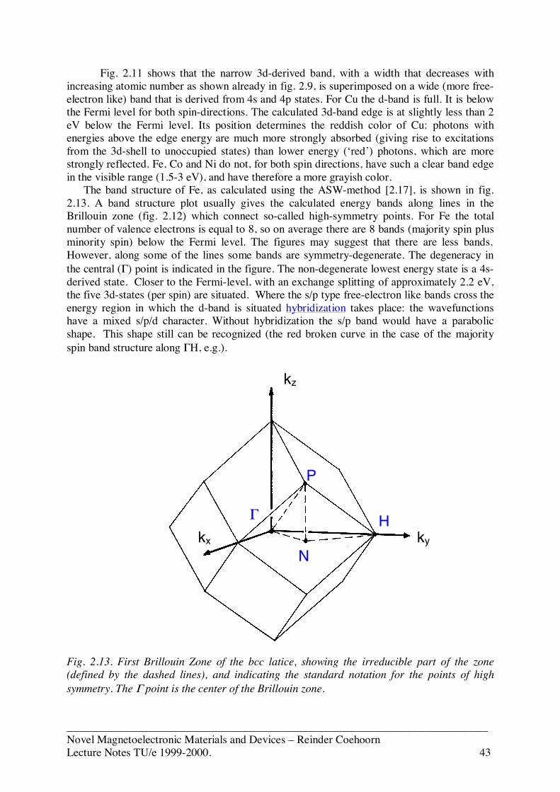
___________________________________________________________________Novel Magnetoelectronic Materials and Devices – Reinder CoehoornLecture Notes TU/e 1999-2000. 43
Fig. 2.11 shows that the narrow 3d-derived band, with a width that decreases withincreasing atomic number as shown already in fig. 2.9, is superimposed on a wide (more free-electron like) band that is derived from 4s and 4p states. For Cu the d-band is full. It is belowthe Fermi level for both spin-directions. The calculated 3d-band edge is at slightly less than 2eV below the Fermi level. Its position determines the reddish color of Cu: photons withenergies above the edge energy are much more strongly absorbed (giving rise to excitationsfrom the 3d-shell to unoccupied states) than lower energy (‘red’) photons, which are morestrongly reflected. Fe, Co and Ni do not, for both spin directions, have such a clear band edgein the visible range (1.5-3 eV), and have therefore a more grayish color.
The band structure of Fe, as calculated using the ASW-method [2.17], is shown in fig.2.13. A band structure plot usually gives the calculated energy bands along lines in theBrillouin zone (fig. 2.12) which connect so-called high-symmetry points. For Fe the totalnumber of valence electrons is equal to 8, so on average there are 8 bands (majority spin plusminority spin) below the Fermi level. The figures may suggest that there are less bands.However, along some of the lines some bands are symmetry-degenerate. The degeneracy inthe central (Γ) point is indicated in the figure. The non-degenerate lowest energy state is a 4s-derived state. Closer to the Fermi-level, with an exchange splitting of approximately 2.2 eV,the five 3d-states (per spin) are situated. Where the s/p type free-electron like bands cross theenergy region in which the d-band is situated hybridization takes place: the wavefunctionshave a mixed s/p/d character. Without hybridization the s/p band would have a parabolicshape. This shape still can be recognized (the red broken curve in the case of the majorityspin band structure along ΓH, e.g.).
Fig. 2.13. First Brillouin Zone of the bcc latice, showing the irreducible part of the zone(defined by the dashed lines), and indicating the standard notation for the points of highsymmetry. The Γ point is the center of the Brillouin zone.
kykx
kz
Γ
P
N
H
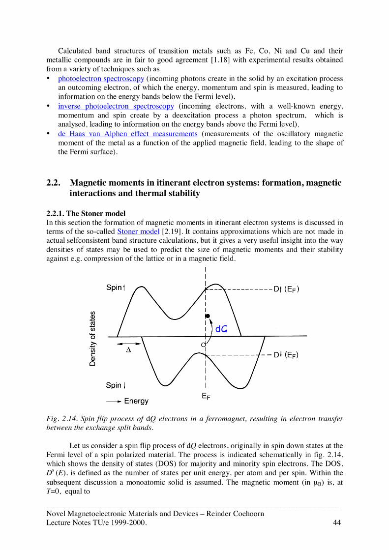
___________________________________________________________________Novel Magnetoelectronic Materials and Devices – Reinder CoehoornLecture Notes TU/e 1999-2000. 44
Calculated band structures of transition metals such as Fe, Co, Ni and Cu and theirmetallic compounds are in fair to good agreement [1.18] with experimental results obtainedfrom a variety of techniques such as• photoelectron spectroscopy (incoming photons create in the solid by an excitation process
an outcoming electron, of which the energy, momentum and spin is measured, leading toinformation on the energy bands below the Fermi level),
• inverse photoelectron spectroscopy (incoming electrons, with a well-known energy,momentum and spin create by a deexcitation process a photon spectrum, which isanalysed, leading to information on the energy bands above the Fermi level),
• de Haas van Alphen effect measurements (measurements of the oscillatory magneticmoment of the metal as a function of the applied magnetic field, leading to the shape ofthe Fermi surface).
2.2. Magnetic moments in itinerant electron systems: formation, magneticinteractions and thermal stability
2.2.1. The Stoner modelIn this section the formation of magnetic moments in itinerant electron systems is discussed interms of the so-called Stoner model [2.19]. It contains approximations which are not made inactual selfconsistent band structure calculations, but it gives a very useful insight into the waydensities of states may be used to predict the size of magnetic moments and their stabilityagainst e.g. compression of the lattice or in a magnetic field.
Fig. 2.14. Spin flip process of dQ electrons in a ferromagnet, resulting in electron transferbetween the exchange split bands.
Let us consider a spin flip process of dQ electrons, originally in spin down states at theFermi level of a spin polarized material. The process is indicated schematically in fig. 2.14,which shows the density of states (DOS) for majority and minority spin electrons. The DOS,Ds (E), is defined as the number of states per unit energy, per atom and per spin. Within thesubsequent discussion a monoatomic solid is assumed. The magnetic moment (in µB) is, atT=0, equal to
dQ
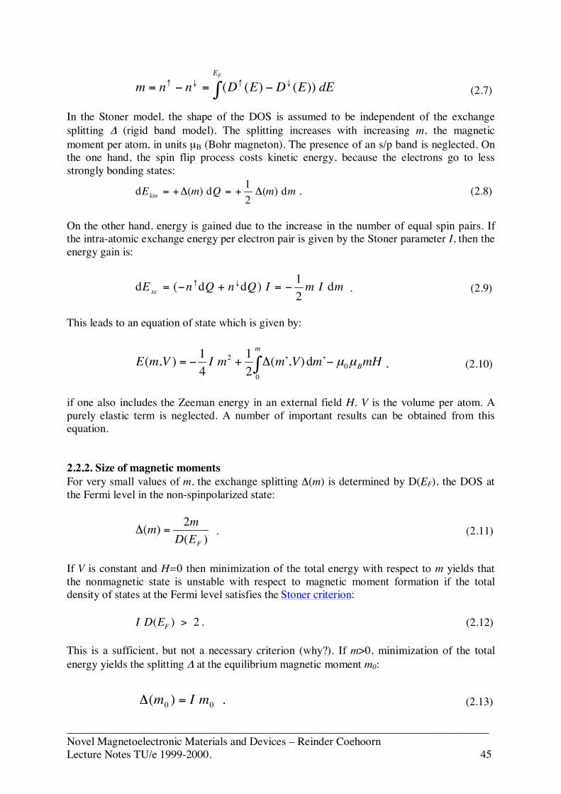
___________________________________________________________________Novel Magnetoelectronic Materials and Devices – Reinder CoehoornLecture Notes TU/e 1999-2000. 45
∫ ↓↑↓↑ −=−=FE
dEEDEDnnm ))()(( (2.7)
In the Stoner model, the shape of the DOS is assumed to be independent of the exchangesplitting Δ (rigid band model). The splitting increases with increasing m, the magneticmoment per atom, in units µB (Bohr magneton). The presence of an s/p band is neglected. Onthe one hand, the spin flip process costs kinetic energy, because the electrons go to lessstrongly bonding states:
mmQmEkin d)(21d)(d Δ+=Δ+= . (2.8)
On the other hand, energy is gained due to the increase in the number of equal spin pairs. Ifthe intra-atomic exchange energy per electron pair is given by the Stoner parameter I, then theenergy gain is:
mImIQnQnE xc d21)dd(d −=+−= ↓↑ . (2.9)
This leads to an equation of state which is given by:
mHmVmmIVmE B
m
µµ00
2 ’d),’(21
41),( −Δ+−= ∫ , (2.10)
if one also includes the Zeeman energy in an external field H. V is the volume per atom. Apurely elastic term is neglected. A number of important results can be obtained from thisequation.
2.2.2. Size of magnetic momentsFor very small values of m, the exchange splitting Δ(m) is determined by D(EF), the DOS atthe Fermi level in the non-spinpolarized state:
)(2)(
FEDmm =Δ . (2.11)
If V is constant and H=0 then minimization of the total energy with respect to m yields thatthe nonmagnetic state is unstable with respect to magnetic moment formation if the totaldensity of states at the Fermi level satisfies the Stoner criterion:
.2)( >FEDI (2.12)
This is a sufficient, but not a necessary criterion (why?). If m>0, minimization of the totalenergy yields the splitting Δ at the equilibrium magnetic moment m0:
.)( 00 mIm =Δ (2.13)
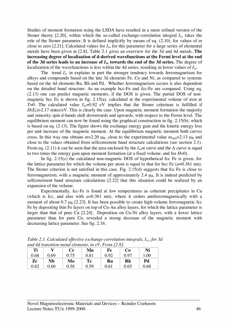
___________________________________________________________________Novel Magnetoelectronic Materials and Devices – Reinder CoehoornLecture Notes TU/e 1999-2000. 46
Studies of moment formation using the LSDA have resulted in a more refined version of theStoner theory [2.20], within which the so-called exchange-correlation integral Ixc takes therole of the Stoner parameter. It is defined implicitly by means of eq. (2.10), for values of mclose to zero [2.21]. Calculated values for Ixc for this parameter for a large series of elementalmetals have been given in [2.8]. Table 2.1 gives an overview for the 3d and 4d metals. Theincreasing degree of localization of d-derived wavefunctions at the Fermi level at the endof the 3d series leads to an increase of Ixc towards the end of the 3d series. The degree oflocalization of the wavefunctions is less within the 4d series, resulting in lower values of Ixc.
The trend Ixc in explains in part the stronger tendency towards ferromagnetism foralloys and compounds based on the late 3d elements Fe, Co and Ni, as compared to systemsbased on the 4d elements Ru, Rh and Pd. Whether ferromagnetism occurs is also dependenton the detailed band structure. As an example bcc-Fe and fcc-Fe are compared. Using eq.(2.13) one can predict magnetic moments, if the DOS is given. The partial DOS of non-magnetic bcc Fe is shown in fig. 2.15(a), calculated at the experimental volume of iron atT=0. The calculated value Ixc=0.92 eV implies that the Stoner criterium is fulfilled ifD(EF)>2.17 states/eV. This is clearly the case. Upon magnetic moment formation the majorityand minority spin d-bands shift downwards and upwards, with respect to the Fermi level. Theequilibrium moment can now be found using the graphical construction in fig. 2.15(b), whichis based on eq. (2.13). The figure shows the exchange energy gain and the kinetic energy lossper unit increase of the magnetic moment. At the equilibrium magnetic moment both curvescross. In this way one obtains m=2.20 µB, close to the experimental value mspin=2.13 µB andclose to the values obtained from selfconsistent band structure calculations (see section 2.1).From eq. (2.11) it can be seen that the area enclosed by the Ixcm curve and the Δ curve is equalto two times the energy gain upon moment formation (at a fixed volume, and for H=0).
In fig. 2.15(c) the calculated non-magnetic DOS of hypothetical fcc Fe is given, forthe lattice parameter for which the volume per atom is equal to that for bcc Fe (a=0.361 nm).The Stoner criterion is not satisfied in this case. Fig. 2.15(d) suggests that fcc Fe is close toferromagnetism, with a magnetic moment of approximately 2.4 µB. It is indeed predicted byselfconsistent band structure calculations [2.22] that this situation could be realized by anexpansion of the volume.
Experimentally, fcc-Fe is found at low temperatures as coherent precipitates in Cu(which is fcc, and also with a=0.361 nm), where it orders antiferromagnetically with amoment of about 0.7 µB [2.23]. It has been possible to create high-volume ferromagnetic fccFe by depositing thin Fe layers on top of Cu-Au alloy layers, for which the lattice parameter islarger than that of pure Cu [2.24]. Deposition on Cu-Ni alloy layers, with a lower latticeparameter than for pure Cu, revealed a strong decrease of the magnetic moment withdecreasing lattice parameter. See fig. 2.16.
Table 2.1. Calculated effective exchange-correlation integrals, Ixc, for 3dand 4d transition metal elements, in eV. From [2.8]. Ti 0.68
V 0.69
Cr 0.75
Mn 0.81
Fe 0.92
Co 0.97
Ni 1.00
Zr 0.62
Nb 0.60
Mo 0.58
Tc 0.59
Ru 0.61
Rh 0.65
Pd 0.68
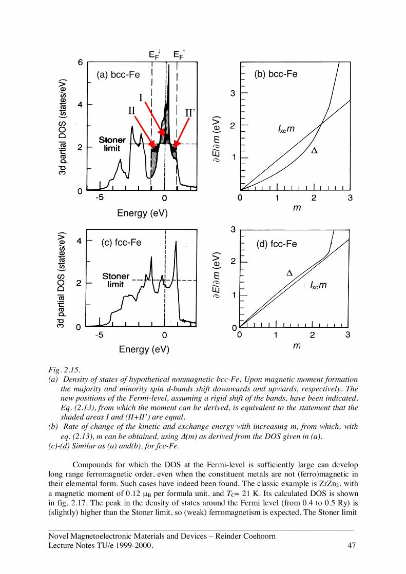
___________________________________________________________________Novel Magnetoelectronic Materials and Devices – Reinder CoehoornLecture Notes TU/e 1999-2000. 47
Fig. 2.15.(a) Density of states of hypothetical nonmagnetic bcc-Fe. Upon magnetic moment formation
the majority and minority spin d-bands shift downwards and upwards, respectively. Thenew positions of the Fermi-level, assuming a rigid shift of the bands, have been indicated.Eq. (2.13), from which the moment can be derived, is equivalent to the statement that theshaded areas I and (II+II’) are equal.
(b) Rate of change of the kinetic and exchange energy with increasing m, from which, witheq. (2.13), m can be obtained, using Δ(m) as derived from the DOS given in (a).
(c)-(d) Similar as (a) and(b), for fcc-Fe.
Compounds for which the DOS at the Fermi-level is sufficiently large can developlong range ferromagnetic order, even when the constituent metals are not (ferro)magnetic intheir elemental form. Such cases have indeed been found. The classic example is ZrZn2, witha magnetic moment of 0.12 µB per formula unit, and TC= 21 K. Its calculated DOS is shownin fig. 2.17. The peak in the density of states around the Fermi level (from 0.4 to 0.5 Ry) is(slightly) higher than the Stoner limit, so (weak) ferromagnetism is expected. The Stoner limit
II’
(a) bcc-Fe
I II
(b) bcc-Fe
(c) fcc-Fe (d) fcc-Fe
Ixcm
Ixcm
m
mEnergy (eV)
Energy (eV)
∂
E/∂m
(eV)
∂E/∂m
(eV)

___________________________________________________________________Novel Magnetoelectronic Materials and Devices – Reinder CoehoornLecture Notes TU/e 1999-2000. 48
Fig. 2.16. Structure of an fcc Fe/Cu artificial superlattice with a 4% enhanced latticeparameter (left). Magnetic moment per Fe atom as a function of the lattice parameter (Δa/a(in %) is with respect to pure Cu) [2.24].
Fig. 2.17. Calculated density of states of the intermetallic compound ZrZn2. Non-magneticcalculation. The actual DOS will be spin-split, leading to a small magnetic moment(experimental value: 0.12 µB per formula unit). 1 Ry= 13.605 eV. One unit cell contains 4formula units ZrZn2. From [2.25].
a (nm)
0.36 0.37 0.380.0.380.380.38.8
Δa/a (%)
Energy (Ry)
ZrZn2
Den
sity
of s
tate
s (s
tate
s/R
y ce
ll)
Stoner limit
EF
___________________________________________________________________Novel Magnetoelectronic Materials and Devices – Reinder CoehoornLecture Notes TU/e 1999-2000. 49
is estimated as follows. The peak at the Fermi level is found, from the calculations, to be dueto wavefunctions which are derived from Zr-4d states. In this energy range, hybridizationwith states that are derived from Zn-4s and Zn-4p states is weak. Neglecting the effect ofhybridization, the Stoner criterion predicts that the non-magnetic state is unstable with respectto the formation of magnetic moments when the density of states per Zr atom is larger than3.22 states/eV (eq. (2.12) and table 2.1), i.e. 176 states/Ry unit cell (red dashed line).Although the figure (and explicit calculations) show that the non-magnetic state is unstablewith respect to the formation of a ferromagnetic state, the ferromagnetic state is notnecessarily the most stable state. Antiferromagnetism (with, in principle, an infinitely largenumber of possible antiferromagnetic structures), could also occur. Indeed, the isoelectronicisostructural compound TiBe2 , which has a similar electronic structure as ZrZn2 [2.25] isantiferromagnetic, with TN = 10 K.
Another example of a weak ferromagnet is VAu4, with a moment of 1.0 µB performula unit and TC= 61 K.
2.2.3. Magnetic susceptibilityFrom eq. (2.10) the spin-contribution to the magnetic susceptibility (per atom) at constantvolume can be derived (Wohlfarth-Gersdorf formula):
⎟⎟⎠
⎞⎜⎜⎝
⎛−+
=∂
∂≡
↓↑ xcFF
BBatom
IEDED
Hm
2)(
1)(
1
4)( 0 µµµχ . (2.14)
The macroscopic susceptibility (dimensionless) is then
⎟⎟⎠
⎞⎜⎜⎝
⎛−+
=∂
∂=
∂
∂≡
↓↑ xcFF
BB
IEDED
NH
NmHM
2)(
1)(
1
4)( 0 µµµχ (2.15)
with N the number of atoms per m3. Unfortunately, the spin contribution to the susceptibilitycannot be measured separately from the orbital contribution (see [2.26], [2.27]). Theseexpressions can also be applied to non-ferromagnetic materials (paramagnetic materials), forwhich the density of states is not spin-polarized. It follows that the susceptibility is ‘exchangeenhanced’. When then density of states approaches the Stoner limit (see eq. (2.12)) thesusceptibility diverges. An example is Pd.
2.2.4. Volume dependence of the magnetizationThe width of d-bands, and consequently also the exchange splitting for a given magneticmoment, Δ(m), is to a good approximation proportional to V–3/5. From eq. (2.12) it thenfollows that
⎟⎟⎠
⎞⎜⎜⎝
⎛−+
×=∂
∂=
∂∂
↓↑ xcFF
BxcB
IEDED
NmIV
NmVMV
2)(
1)(
12
35)( µµ
. (2.16)

___________________________________________________________________Novel Magnetoelectronic Materials and Devices – Reinder CoehoornLecture Notes TU/e 1999-2000. 50
A general conclusion which follows from eqs (2.15) and (2.16) is that moments in systems forwhich either the majority and/or the minority spin DOS at the Fermi level are small are stableagainst a (small) variation of the external field or the volume. Moments in bcc Fe derive theirstability mainly from the low value of D↓(EF), see fig. 2.11. Moments in Co and Ni, for whichthe majority spin d band is fully occupied, derive their stability from the low value of D↑(EF),see fig. 2.11. Co and Ni are called strong (saturated) ferromagnets, wheras Fe, with anunfilled majority spin d band, is called a weak (unsaturated) ferromagnet.
2.2.5. Finite temperatures – Stoner Curie temperatureThe Stoner theory can be extended to finite temperatures [2.19]. Thermally induced spin-conserving excitations of electrons (single particle excitations), described by the Fermi-Diracdistribution f(E), can be taken into account by replacing eq. (2.7) by the more general Stonerequations:
∫∞↓↑ Δ
+−Δ
−=−=0
)(21)]
2()
2([ dEEDEfEfnnm (2.17a)
∫∞↓↑ Δ
++Δ
−=+=0
)(21)]
2()
2([ dEEDEfEfnnn (2.17b)
with D(E) the total DOS per atom (in the absence of a spin splitting), Δ=Ixcm (eq. 2.13) and
1exp
1)(+⎟⎟
⎠
⎞⎜⎜⎝
⎛ −=
Tk
f
B
µεε . (2.18)
Here µ is the chemical potential. From these expressions the unknown temperature dependentm and µ can be derived. The ‘smearing of the Fermi level’ leads to a spatially uniformlowering of the magnetic moment with increasing temperature. At the Stoner Curietemperature, TC,S, the magnetization becomes zero. The values of TC,S which are found for Fe,Co and Ni are, however, much higher than the experimental value [2.20], viz. 4400-6200,3300-4800 and 2900 K, respectively, whereas the experimental values are 1040, 1390 and 630K, respectively. There are other weakness of the Stoner theory (see e.g. [2.28]). An example isthe incorrect prediction of the variation of the magnetization at low temperatures: M(0)-M(T)∝T2 is predicted, but experimentally M(0)-M(T)∝T3/2, (Bloch T3/2 law) as expected onthe basis of spin wave excitations. The Stoner Curie temperature provides only an upper limit.In Fe, Co and Ni, and in many other materials of practical interest, fluctations of themagnetization direction, and not in the first place of the size of the magnetic moment,determine the Curie temperature.
2.2.6. Magnetic moments and TC in itinerant electron systems, case I: Heusler alloysWithin the Stoner model the thermal fluctuations that are considered are due to spin-conserving excitations between pairs of quantum-mechanical Bloch states with wavevectors kand k+q, respectively. As both states extend over the entire crystal, the effect of suchexcitations is a spatially uniform change of the magnetization.
Let us now consider spin-non-conserving excitations (‘magnetic excitations’) betweenpairs of Bloch states. Linear combinations of such excitations can be described as quantizedspin waves (magnons). A classical treatment of the magnon energy as a function of the
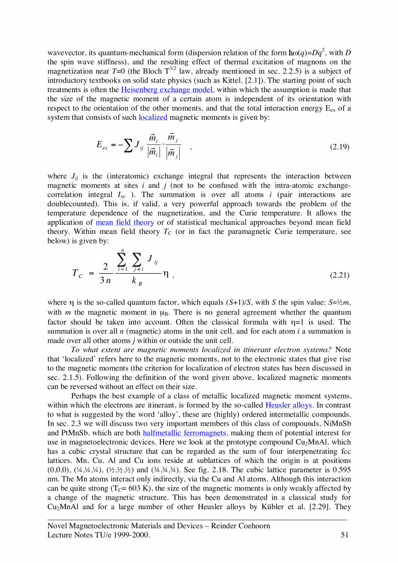
___________________________________________________________________Novel Magnetoelectronic Materials and Devices – Reinder CoehoornLecture Notes TU/e 1999-2000. 51
wavevector, its quantum-mechanical form (dispersion relation of the form ω(q)=Dq2, with Dthe spin wave stiffness), and the resulting effect of thermal excitation of magnons on themagnetization near T=0 (the Bloch T3/2 law, already mentioned in sec. 2.2.5) is a subject ofintroductory textbooks on solid state physics (such as Kittel, [2.1]). The starting point of suchtreatments is often the Heisenberg exchange model, within which the assumption is made thatthe size of the magnetic moment of a certain atom is independent of its orientation withrespect to the orientation of the other moments, and that the total interaction energy Eex of asystem that consists of such localized magnetic moments is given by:
∑ ⋅−=j
j
i
iijex m
mmm
JE , (2.19)
where Jij is the (interatomic) exchange integral that represents the interaction betweenmagnetic moments at sites i and j (not to be confused with the intra-atomic exchange-correlation integral Ixc ). The summation is over all atoms i (pair interactions aredoublecounted). This is, if valid, a very powerful approach towards the problem of thetemperature dependence of the magnetization, and the Curie temperature. It allows theapplication of mean field theory or of statistical mechanical approaches beyond mean fieldtheory. Within mean field theory TC (or in fact the paramagnetic Curie temperature, seebelow) is given by:
η=∑ ∑
= ≠
B
n
i ijij
C k
J
nT 1
32
, (2.21)
where η is the so-called quantum factor, which equals (S+1)/S, with S the spin value: S=½m,with m the magnetic moment in µB. There is no general agreement whether the quantumfactor should be taken into account. Often the classical formula with η=1 is used. Thesummation is over all n (magnetic) atoms in the unit cell, and for each atom i a summation ismade over all other atoms j within or outside the unit cell.
To what extent are magnetic moments localized in itinerant electron systems? Notethat ‘localized’ refers here to the magnetic moments, not to the electronic states that give riseto the magnetic moments (the criterion for localization of electron states has been discussed insec. 2.1.5). Following the definition of the word given above, localized magnetic momentscan be reversed without an effect on their size.
Perhaps the best example of a class of metallic localized magnetic moment systems,within which the electrons are itinerant, is formed by the so-called Heusler alloys. In contrastto what is suggested by the word ‘alloy’, these are (highly) ordered intermetallic compounds.In sec. 2.3 we will discuss two very important members of this class of compounds, NiMnSband PtMnSb, which are both halfmetallic ferromagnets, making them of potential interest foruse in magnetoelectronic devices. Here we look at the prototype compound Cu2MnAl, whichhas a cubic crystal structure that can be regarded as the sum of four interpenetrating fcclattices. Mn, Cu, Al and Cu ions reside at sublattices of which the origin is at positions(0,0,0), (¼,¼,¼), (½,½,½) and (¾,¾,¾). See fig. 2.18. The cubic lattice parameter is 0.595nm. The Mn atoms interact only indirectly, via the Cu and Al atoms. Although this interactioncan be quite strong (TC= 603 K), the size of the magnetic moments is only weakly affected bya change of the magnetic structure. This has been demonstrated in a classical study forCu2MnAl and for a large number of other Heusler alloys by Kübler et al. [2.29]. They
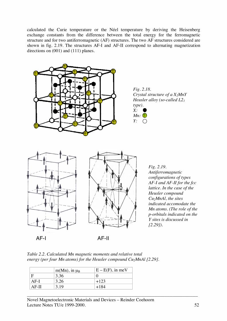
___________________________________________________________________Novel Magnetoelectronic Materials and Devices – Reinder CoehoornLecture Notes TU/e 1999-2000. 52
calculated the Curie temperature or the Néel temperature by deriving the Heisenbergexchange constants from the difference between the total energy for the ferromagneticstructure and for two antiferromagnetic (AF) structures. The two AF structures considered areshown in fig. 2.19. The structures AF-I and AF-II correspond to alternating magnetizationdirections on (001) and (111) planes.
•
Table 2.2. Calculated Mn magnetic moments and relative totalenergy (per four Mn atoms) for the Heusler compound Cu2MnAl [2.29].
m(Mn), in µB E – E(F), in meVF 3.36 0AF-I 3.26 +123AF-II 3.19 +184
Fig. 2.18.Crystal structure of a X2MnYHeusler alloy (so-called L21type).X:Mn:Y:
Fig. 2.19.Antiferromagneticconfigurations of typesAF-I and AF-II for the fcclattice. In the case of theHeusler compoundCu2MnAl, the sitesindicated accomodate theMn atoms. (The role of thep-orbitals indicated on theY sites is discussed in[2.29]).
AF-I AF-II
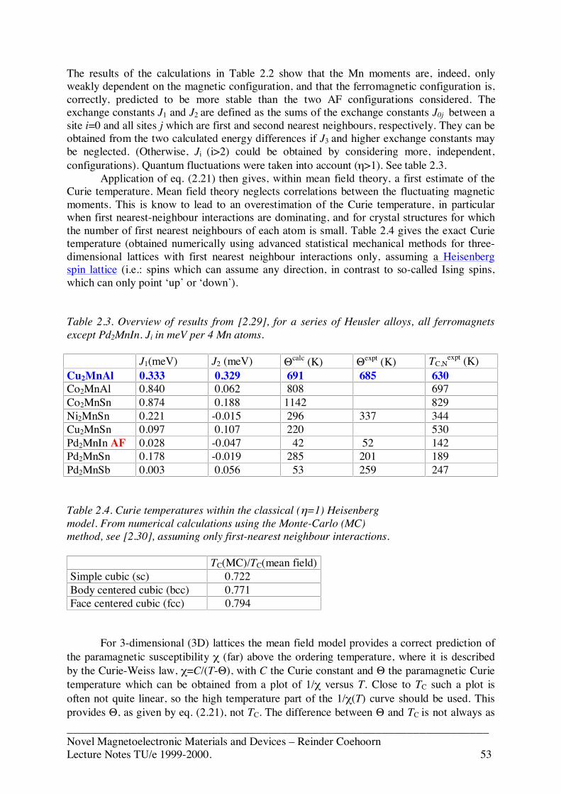
___________________________________________________________________Novel Magnetoelectronic Materials and Devices – Reinder CoehoornLecture Notes TU/e 1999-2000. 53
The results of the calculations in Table 2.2 show that the Mn moments are, indeed, onlyweakly dependent on the magnetic configuration, and that the ferromagnetic configuration is,correctly, predicted to be more stable than the two AF configurations considered. Theexchange constants J1 and J2 are defined as the sums of the exchange constants J0j between asite i=0 and all sites j which are first and second nearest neighbours, respectively. They can beobtained from the two calculated energy differences if J3 and higher exchange constants maybe neglected. (Otherwise, Ji (i>2) could be obtained by considering more, independent,configurations). Quantum fluctuations were taken into account (η>1). See table 2.3.
Application of eq. (2.21) then gives, within mean field theory, a first estimate of theCurie temperature. Mean field theory neglects correlations between the fluctuating magneticmoments. This is know to lead to an overestimation of the Curie temperature, in particularwhen first nearest-neighbour interactions are dominating, and for crystal structures for whichthe number of first nearest neighbours of each atom is small. Table 2.4 gives the exact Curietemperature (obtained numerically using advanced statistical mechanical methods for three-dimensional lattices with first nearest neighbour interactions only, assuming a Heisenbergspin lattice (i.e.: spins which can assume any direction, in contrast to so-called Ising spins,which can only point ‘up’ or ‘down’).
Table 2.3. Overview of results from [2.29], for a series of Heusler alloys, all ferromagnetsexcept Pd2MnIn. Ji in meV per 4 Mn atoms.
J1(meV) J2 (meV) Θcalc (K) Θexpt (K) TC,Nexpt (K)
Cu2MnAl 0.333 0.329 691 685 630Co2MnAl 0.840 0.062 808 697Co2MnSn 0.874 0.188 1142 829Ni2MnSn 0.221 -0.015 296 337 344Cu2MnSn 0.097 0.107 220 530Pd2MnIn AF 0.028 -0.047 42 52 142Pd2MnSn 0.178 -0.019 285 201 189Pd2MnSb 0.003 0.056 53 259 247
Table 2.4. Curie temperatures within the classical (η=1) Heisenbergmodel. From numerical calculations using the Monte-Carlo (MC)method, see [2.30], assuming only first-nearest neighbour interactions.
TC(MC)/TC(mean field)Simple cubic (sc) 0.722Body centered cubic (bcc) 0.771Face centered cubic (fcc) 0.794
For 3-dimensional (3D) lattices the mean field model provides a correct prediction ofthe paramagnetic susceptibility χ (far) above the ordering temperature, where it is describedby the Curie-Weiss law, χ=C/(T-Θ), with C the Curie constant and Θ the paramagnetic Curietemperature which can be obtained from a plot of 1/χ versus T. Close to TC such a plot isoften not quite linear, so the high temperature part of the 1/χ(T) curve should be used. Thisprovides Θ, as given by eq. (2.21), not TC. The difference between Θ and TC is not always as
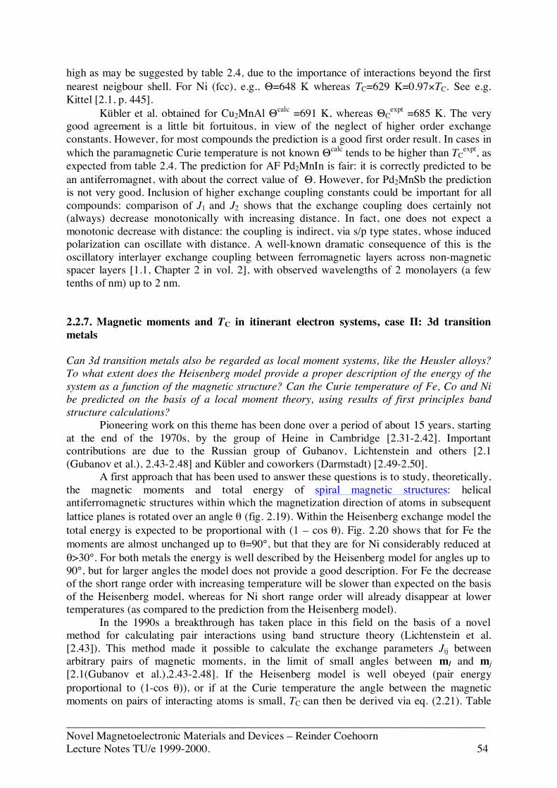
___________________________________________________________________Novel Magnetoelectronic Materials and Devices – Reinder CoehoornLecture Notes TU/e 1999-2000. 54
high as may be suggested by table 2.4, due to the importance of interactions beyond the firstnearest neigbour shell. For Ni (fcc), e.g., Θ=648 K whereas TC=629 K=0.97×TC. See e.g.Kittel [2.1, p. 445].
Kübler et al. obtained for Cu2MnAl Θcalc =691 K, whereas ΘCexpt =685 K. The very
good agreement is a little bit fortuitous, in view of the neglect of higher order exchangeconstants. However, for most compounds the prediction is a good first order result. In cases inwhich the paramagnetic Curie temperature is not known Θcalc tends to be higher than TC
expt, asexpected from table 2.4. The prediction for AF Pd2MnIn is fair: it is correctly predicted to bean antiferromagnet, with about the correct value of Θ. However, for Pd2MnSb the predictionis not very good. Inclusion of higher exchange coupling constants could be important for allcompounds: comparison of J1 and J2 shows that the exchange coupling does certainly not(always) decrease monotonically with increasing distance. In fact, one does not expect amonotonic decrease with distance: the coupling is indirect, via s/p type states, whose inducedpolarization can oscillate with distance. A well-known dramatic consequence of this is theoscillatory interlayer exchange coupling between ferromagnetic layers across non-magneticspacer layers [1.1, Chapter 2 in vol. 2], with observed wavelengths of 2 monolayers (a fewtenths of nm) up to 2 nm.
2.2.7. Magnetic moments and TC in itinerant electron systems, case II: 3d transitionmetals
Can 3d transition metals also be regarded as local moment systems, like the Heusler alloys?To what extent does the Heisenberg model provide a proper description of the energy of thesystem as a function of the magnetic structure? Can the Curie temperature of Fe, Co and Nibe predicted on the basis of a local moment theory, using results of first principles bandstructure calculations?
Pioneering work on this theme has been done over a period of about 15 years, startingat the end of the 1970s, by the group of Heine in Cambridge [2.31-2.42]. Importantcontributions are due to the Russian group of Gubanov, Lichtenstein and others [2.1(Gubanov et al.), 2.43-2.48] and Kübler and coworkers (Darmstadt) [2.49-2.50].
A first approach that has been used to answer these questions is to study, theoretically,the magnetic moments and total energy of spiral magnetic structures: helicalantiferromagnetic structures within which the magnetization direction of atoms in subsequentlattice planes is rotated over an angle θ (fig. 2.19). Within the Heisenberg exchange model thetotal energy is expected to be proportional with (1 – cos θ). Fig. 2.20 shows that for Fe themoments are almost unchanged up to θ=90°, but that they are for Ni considerably reduced atθ>30°. For both metals the energy is well described by the Heisenberg model for angles up to90°, but for larger angles the model does not provide a good description. For Fe the decreaseof the short range order with increasing temperature will be slower than expected on the basisof the Heisenberg model, whereas for Ni short range order will already disappear at lowertemperatures (as compared to the prediction from the Heisenberg model).
In the 1990s a breakthrough has taken place in this field on the basis of a novelmethod for calculating pair interactions using band structure theory (Lichtenstein et al.[2.43]). This method made it possible to calculate the exchange parameters Jij betweenarbitrary pairs of magnetic moments, in the limit of small angles between mI and mj[2.1(Gubanov et al.),2.43-2.48]. If the Heisenberg model is well obeyed (pair energyproportional to (1-cos θ)), or if at the Curie temperature the angle between the magneticmoments on pairs of interacting atoms is small, TC can then be derived via eq. (2.21). Table

___________________________________________________________________Novel Magnetoelectronic Materials and Devices – Reinder CoehoornLecture Notes TU/e 1999-2000. 55
2.5 gives calculated Curie temperatures as obtained by Sabiryanov et al. [2.44]. As discussedin section 2.2.6 mean field overestimates the Curie temperature, as it neglects correlationbetween moments. The error can be a 20-30 %, depending on the crystal structure, in the caseof nearest neighbour interactions only, and less if interactions beyond the first nearestneighbour shell are important. Taking this into account, the agreement between theory andexperiment for the cases given in table 2.5 seems quite good.
Fig. 2.19. Spin spiral structures. From [2.33].
Fig. 2.20. Calculated total energy (relative units) and magnetic moments for spin spiralstructures of bcc Fe and fcc Ni (from Gubanov et al., [2.1]).
Table 2.5. Curie temperatures of crystalline elemental metals.Theoretical values are obtainedwithin mean field theory from calculated exchange constants [2.29].
TC,theory (K) TC,experiment (K)Bcc Fe 1270 1040Hcp Co 1520 1360Fcc Co 1530 1388
θ
Spin spiral
θ
1 – cos θ
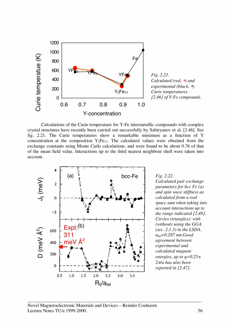
___________________________________________________________________Novel Magnetoelectronic Materials and Devices – Reinder CoehoornLecture Notes TU/e 1999-2000. 56
Calculations of the Curie temperature for Y-Fe intermetallic compounds with complexcrystal structures have recently been carried out successfully by Sabiryanov et al. [2.46]. Seefig. 2.21. The Curie temperatures show a remarkable minimum as a function of Yconcentration at the composition Y2Fe17. The calculated values were obtained from theexchange constants using Monte Carlo calculations, and were found to be about 0.76 of thatof the mean field value. Interactions up to the third nearest neighbour shell were taken intoaccount.
Rij/alat
D
(meV
Å2 )
Jij (
meV
) bcc-Fe(a)
(b)Expt:311meV Å2
0
200
400
600
800
1000
1200
0,6 0,7 0,8 0,9 1
Cur
ie te
mpe
ratu
e (K
)
YFe2 YFe3
Y2Fe17
YFe12
Fe
Fig. 2.21.Calculated (red, •) andexperimental (black, •)Curie temperatures[2.46] of Y-Fe compounds.
0.6 0.7 0.8 0.9 1.0 Y-concentration
Fig. 2.22.Calculated pair exchangeparameters for bcc Fe (a)and spin wave stiffness ascalculated from a realspace sum when taking intoaccount interactions up tothe range indicated [2.48].Circles (triangles): with(without) using the GGA(sec. 2.1.3) in the LSDA.alat=0.287 nm.Goodagreement betweenexperimental andcalculated magnonenergies, up to q=0.25×2π/a has also beenreported in [2.47].
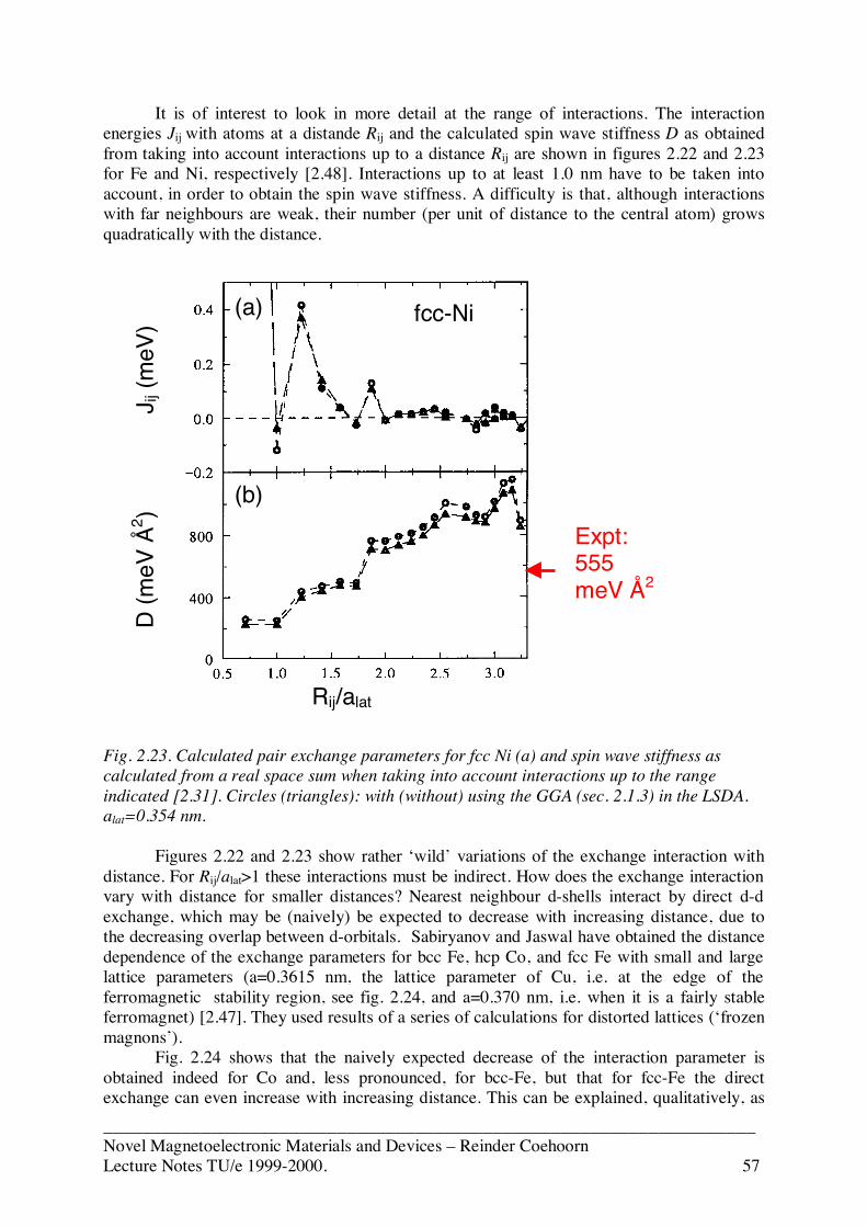
___________________________________________________________________Novel Magnetoelectronic Materials and Devices – Reinder CoehoornLecture Notes TU/e 1999-2000. 57
It is of interest to look in more detail at the range of interactions. The interactionenergies Jij with atoms at a distande Rij and the calculated spin wave stiffness D as obtainedfrom taking into account interactions up to a distance Rij are shown in figures 2.22 and 2.23for Fe and Ni, respectively [2.48]. Interactions up to at least 1.0 nm have to be taken intoaccount, in order to obtain the spin wave stiffness. A difficulty is that, although interactionswith far neighbours are weak, their number (per unit of distance to the central atom) growsquadratically with the distance.
Fig. 2.23. Calculated pair exchange parameters for fcc Ni (a) and spin wave stiffness ascalculated from a real space sum when taking into account interactions up to the rangeindicated [2.31]. Circles (triangles): with (without) using the GGA (sec. 2.1.3) in the LSDA.alat=0.354 nm.
Figures 2.22 and 2.23 show rather ‘wild’ variations of the exchange interaction withdistance. For Rij/alat>1 these interactions must be indirect. How does the exchange interactionvary with distance for smaller distances? Nearest neighbour d-shells interact by direct d-dexchange, which may be (naively) be expected to decrease with increasing distance, due tothe decreasing overlap between d-orbitals. Sabiryanov and Jaswal have obtained the distancedependence of the exchange parameters for bcc Fe, hcp Co, and fcc Fe with small and largelattice parameters (a=0.3615 nm, the lattice parameter of Cu, i.e. at the edge of theferromagnetic stability region, see fig. 2.24, and a=0.370 nm, i.e. when it is a fairly stableferromagnet) [2.47]. They used results of a series of calculations for distorted lattices (‘frozenmagnons’).
Fig. 2.24 shows that the naively expected decrease of the interaction parameter isobtained indeed for Co and, less pronounced, for bcc-Fe, but that for fcc-Fe the directexchange can even increase with increasing distance. This can be explained, qualitatively, as
Rij/alat
D (m
eV Å
2 )
J
ij (m
eV) fcc-Ni(a)
(b)Expt:555meV Å2
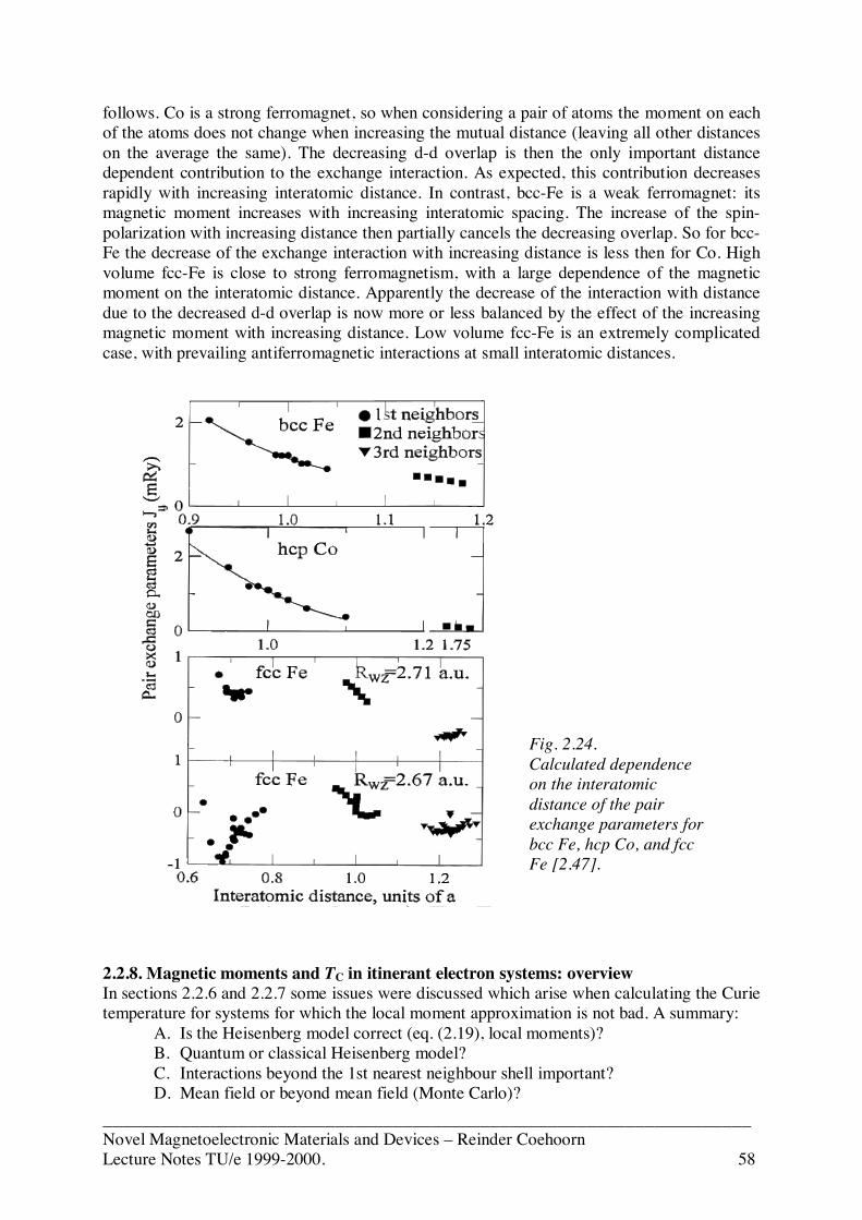
___________________________________________________________________Novel Magnetoelectronic Materials and Devices – Reinder CoehoornLecture Notes TU/e 1999-2000. 58
follows. Co is a strong ferromagnet, so when considering a pair of atoms the moment on eachof the atoms does not change when increasing the mutual distance (leaving all other distanceson the average the same). The decreasing d-d overlap is then the only important distancedependent contribution to the exchange interaction. As expected, this contribution decreasesrapidly with increasing interatomic distance. In contrast, bcc-Fe is a weak ferromagnet: itsmagnetic moment increases with increasing interatomic spacing. The increase of the spin-polarization with increasing distance then partially cancels the decreasing overlap. So for bcc-Fe the decrease of the exchange interaction with increasing distance is less then for Co. Highvolume fcc-Fe is close to strong ferromagnetism, with a large dependence of the magneticmoment on the interatomic distance. Apparently the decrease of the interaction with distancedue to the decreased d-d overlap is now more or less balanced by the effect of the increasingmagnetic moment with increasing distance. Low volume fcc-Fe is an extremely complicatedcase, with prevailing antiferromagnetic interactions at small interatomic distances.
2.2.8. Magnetic moments and TC in itinerant electron systems: overviewIn sections 2.2.6 and 2.2.7 some issues were discussed which arise when calculating the Curietemperature for systems for which the local moment approximation is not bad. A summary:
A. Is the Heisenberg model correct (eq. (2.19), local moments)?B. Quantum or classical Heisenberg model?C. Interactions beyond the 1st nearest neighbour shell important?D. Mean field or beyond mean field (Monte Carlo)?
Fig. 2.24.Calculated dependenceon the interatomicdistance of the pairexchange parameters forbcc Fe, hcp Co, and fccFe [2.47].
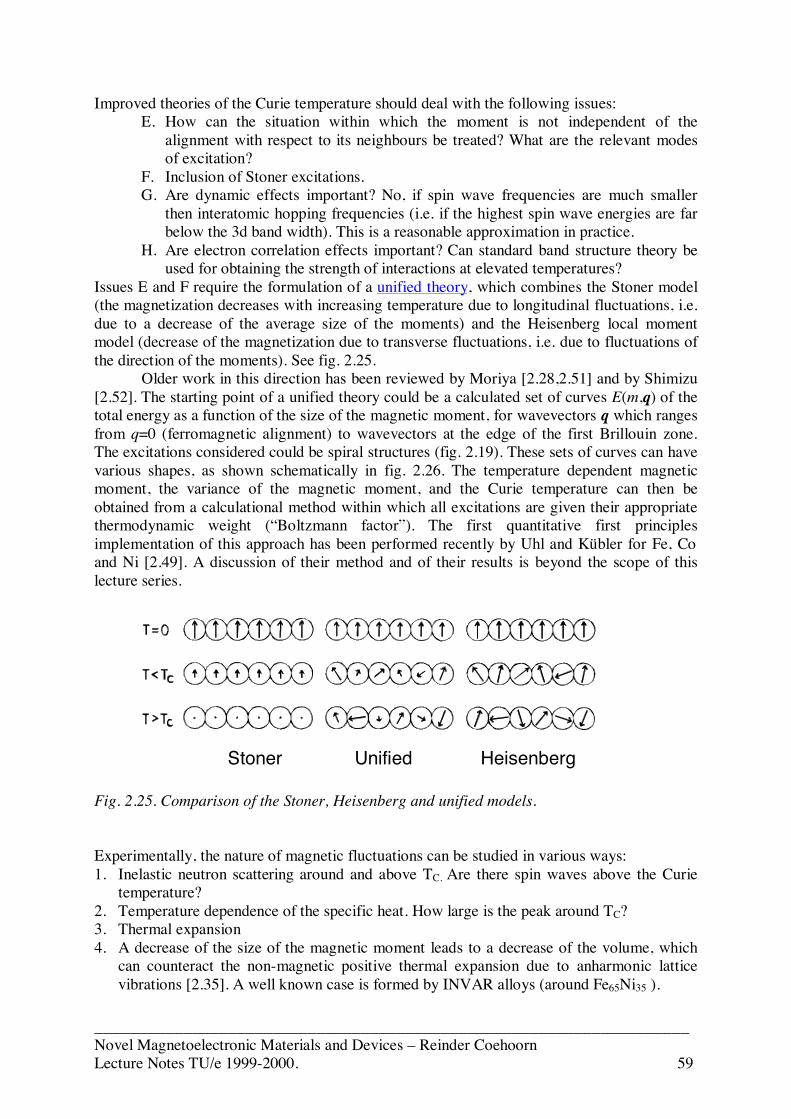
___________________________________________________________________Novel Magnetoelectronic Materials and Devices – Reinder CoehoornLecture Notes TU/e 1999-2000. 59
Improved theories of the Curie temperature should deal with the following issues:E. How can the situation within which the moment is not independent of the
alignment with respect to its neighbours be treated? What are the relevant modesof excitation?
F. Inclusion of Stoner excitations.G. Are dynamic effects important? No, if spin wave frequencies are much smaller
then interatomic hopping frequencies (i.e. if the highest spin wave energies are farbelow the 3d band width). This is a reasonable approximation in practice.
H. Are electron correlation effects important? Can standard band structure theory beused for obtaining the strength of interactions at elevated temperatures?
Issues E and F require the formulation of a unified theory, which combines the Stoner model(the magnetization decreases with increasing temperature due to longitudinal fluctuations, i.e.due to a decrease of the average size of the moments) and the Heisenberg local momentmodel (decrease of the magnetization due to transverse fluctuations, i.e. due to fluctuations ofthe direction of the moments). See fig. 2.25.
Older work in this direction has been reviewed by Moriya [2.28,2.51] and by Shimizu[2.52]. The starting point of a unified theory could be a calculated set of curves E(m,q) of thetotal energy as a function of the size of the magnetic moment, for wavevectors q which rangesfrom q=0 (ferromagnetic alignment) to wavevectors at the edge of the first Brillouin zone.The excitations considered could be spiral structures (fig. 2.19). These sets of curves can havevarious shapes, as shown schematically in fig. 2.26. The temperature dependent magneticmoment, the variance of the magnetic moment, and the Curie temperature can then beobtained from a calculational method within which all excitations are given their appropriatethermodynamic weight (“Boltzmann factor”). The first quantitative first principlesimplementation of this approach has been performed recently by Uhl and Kübler for Fe, Coand Ni [2.49]. A discussion of their method and of their results is beyond the scope of thislecture series.
Fig. 2.25. Comparison of the Stoner, Heisenberg and unified models.
Experimentally, the nature of magnetic fluctuations can be studied in various ways:1. Inelastic neutron scattering around and above TC. Are there spin waves above the Curie
temperature?2. Temperature dependence of the specific heat. How large is the peak around TC?3. Thermal expansion4. A decrease of the size of the magnetic moment leads to a decrease of the volume, which
can counteract the non-magnetic positive thermal expansion due to anharmonic latticevibrations [2.35]. A well known case is formed by INVAR alloys (around Fe65Ni35 ).
Stoner Unified Heisenberg
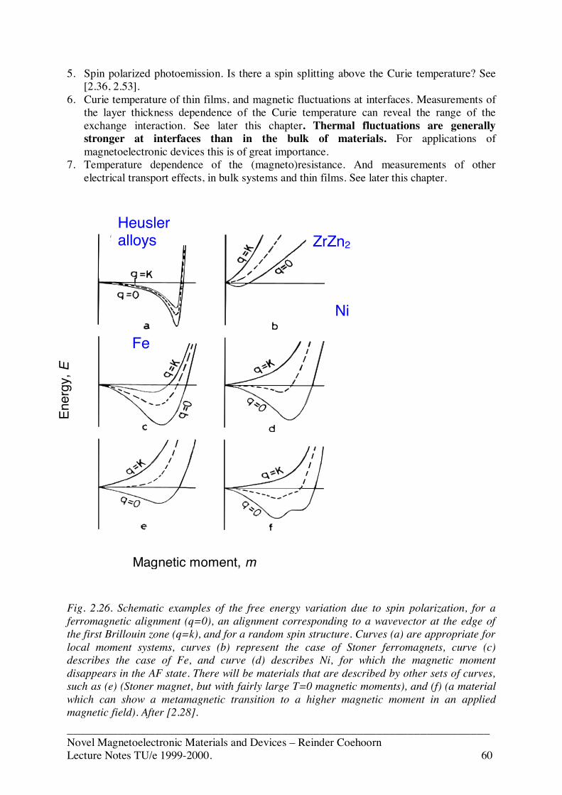
___________________________________________________________________Novel Magnetoelectronic Materials and Devices – Reinder CoehoornLecture Notes TU/e 1999-2000. 60
5. Spin polarized photoemission. Is there a spin splitting above the Curie temperature? See[2.36, 2.53].
6. Curie temperature of thin films, and magnetic fluctuations at interfaces. Measurements ofthe layer thickness dependence of the Curie temperature can reveal the range of theexchange interaction. See later this chapter. Thermal fluctuations are generallystronger at interfaces than in the bulk of materials. For applications ofmagnetoelectronic devices this is of great importance.
7. Temperature dependence of the (magneto)resistance. And measurements of otherelectrical transport effects, in bulk systems and thin films. See later this chapter.
Fig. 2.26. Schematic examples of the free energy variation due to spin polarization, for aferromagnetic alignment (q=0), an alignment corresponding to a wavevector at the edge ofthe first Brillouin zone (q=k), and for a random spin structure. Curves (a) are appropriate forlocal moment systems, curves (b) represent the case of Stoner ferromagnets, curve (c)describes the case of Fe, and curve (d) describes Ni, for which the magnetic momentdisappears in the AF state. There will be materials that are described by other sets of curves,such as (e) (Stoner magnet, but with fairly large T=0 magnetic moments), and (f) (a materialwhich can show a metamagnetic transition to a higher magnetic moment in an appliedmagnetic field). After [2.28].
Heusleralloys
Fe
Ni
ZrZn2
Ener
gy, E
Magnetic moment, m

___________________________________________________________________Novel Magnetoelectronic Materials and Devices – Reinder CoehoornLecture Notes TU/e 1999-2000. 61
2.3. Halfmetallic ferromagnets
2.3.1. OverviewConceptually, a perfect magnetoelectronic switch could by formed by a junction consisting oftwo ferromagnetic layers, within which the electrical conduction is 100 % spin-polarized,separated by a non-magnetic layer which magnetically decouples the two ferromagnetic layersso that it becomes possible to change their relative magnetization directions in a magneticfield. The spacer layer could be metallic or insulating (but then sufficiently thin, so thattunneling across this layer is possible), and the device geometry used could be as discussed insection 1 (e.g. CPP-GMR structure, magnetic tunnel junction, Johnson spin switch (layerstack or lateral structure), Monsma spin transistor, etc.). In the absence of spin flip in theseparation layer or in the electrode layers near the interfaces the devices could be switchedfrom conductive to insulating by switching the relative direction of the magnetization of theelectrode layers from parallel to antiparallel.
Fig. 2.27. Possible spin-polarized density of states of a halfmetallic ferromagnet.
This outlook makes it of great interest to study so-called halfmetallic ferromagnets(HMF). These are materials which are metallic for one type of spin, and an insulator (orsemiconductor) for the other type of spin (fig. 2.27). The electrical conduction is then 100 %spin-polarized. The term ‘halfmetallic ferromagnet’ was introduced in 1983 by de Groot et al.[2.54], who discovered this property theoretically (by performing band structure calculations)for the Heusler alloys NiMnSb and PtMnSb. There is strong experimental evidence that thesetheoretical predictions are correct. These are still the prototype examples of itinerant electronHMF systems, and will be discussed in some detail in section 2.3.2. Whereas the discovery ofhalfmetallic ferromagnetism in these itinerant electron systems, with wide bands, was a bigsurprise, this property was already known for the narrow band oxide compound magnetite,Fe3O4 and was soon shown to be possessed also by CrO2 (sections 2.3.4 and 2.3.3,respectively).
A more recent development is the discovery of halfmetallic ferromagnetism in oxideswhich show the colossal magnetoresistance (CMR) effect, an insulator-metal transition in alarge applied magnetic field, leading to a huge change of the electrical conduction. This effect
Fermi level
En
ergy
___________________________________________________________________Novel Magnetoelectronic Materials and Devices – Reinder CoehoornLecture Notes TU/e 1999-2000. 62
is observed e.g. in manganite compounds such as La1-xSrxMnO3 or La1-xCaxMnO3. Theconduction in the metallic (high field) state conduction is 100 % spin-polarized. A discussionof the CMR effect is not within the scope of this lecture series. However, a brief discussion ofthe HMF character of these oxidic compounds is included in section 2.3.5 for the sake ofcompleteness. It is emphasized that in fact for all oxidic ferromagnets electron correlationbeyond the LSDA is very important (U≈W or U>W, see section 2.1.5), and their electricaltransport properties are not properly described in terms of band structure theory.
2.3.2. NiMnSb, PtMnSb and related Heusler alloysThe halfmetallic ferromagnetism of NiMnSb and PtMnSb is intimately connected to theirspecial so-called C1b crystal structure. This is strongly related to the so-called L21 crystalstructure shown in fig. 2.18 of ordinary Heusler alloys with the composition X2YZ. In bothcases the overall crystal structure is cubic, and the atoms reside on interpenetrating fcclattices. For the L21 crystal structure the atoms reside on the four fcc lattices characterized bythe positions X1(¼ ¼ ¼), Y(0 0 0), X2(¾ ¾ ¾ ) and Z(½ ½ ½), and for the C1b crystalstructure the same situation holds, except that the X1 position are empty. This lowers the pointsymmetry of the Mn atoms at the Y sites from cubic, for the the L21 structure, to tetrahedralfor the C1b crystal structure.
Fig. 2.28 shows the band structure of NiMnSb, as obtained by de Groot et al. using anASW band structure calculation [2.54]. The minority spin band structure shows an (indirect)gap around the Fermi level, whereas the system is metallic for majority spin electrons. Thecalculated magnetic moment is (exactly) 4 µB per Mn atom. For all halfmetallic ferromagnetsthe magnetic moment per unit cell, m = nmaj – nmin (with nmaj and nmin the numbers of majorityspin electrons per unit cell), is an integer, because nmaj and nmin must both be an integer. Thisalready provides a first test of the calculations. Magnetization measurements and neutrondiffraction yield experimental moments of 3.85 µB and about 4.0 µB per Mn atom,respectively [2.55,2.56].
Generally, within a series of isostructural compounds based on isoelectronicconstituents the band structures are very similar. Indeed, when replacing Ni by Pt halfmetallicferromagnetism is also found. The calculated minority spin band structure around the Γ pointis shown in fig. 2.29 (upper left). The experimental magnetic moment of PtMnSb 3.95 µB[2.58], within the experimental error in agreement with the moment of 4 µB expected when itwould be a HMF. In contrast, the replacement of Sb by Sn (which contributes one electronless to the valence band), leads to a Fermi level that crosses the top of the minority spinvalence band (fig. 2.29, lower left): PtMnSn is not a HMF. The calculated (experimental)magnetic moment for PtMnSn is 3.60 (3.42) µB, clearly not an integer. Ir and Rh contributeone valence electron less then Ni, and Os contributes two valence electrons less then Ni. Noneof these non-isoelectric C1b compounds is a HMF. The number of electrons contributed to thevalence band by the nonmagnetic atoms is clearly very important.
Although not all compounds for which a part of the band structure is given in fig. 2.29are HMF, all show a distinct gap in the minority spin density of states. Such a gap is notcommonly found for transition metal based intermetallic compounds, even not for ordinaryHeusler alloys of the type X2YZ. What makes the C1b structure so special? Let us first look at
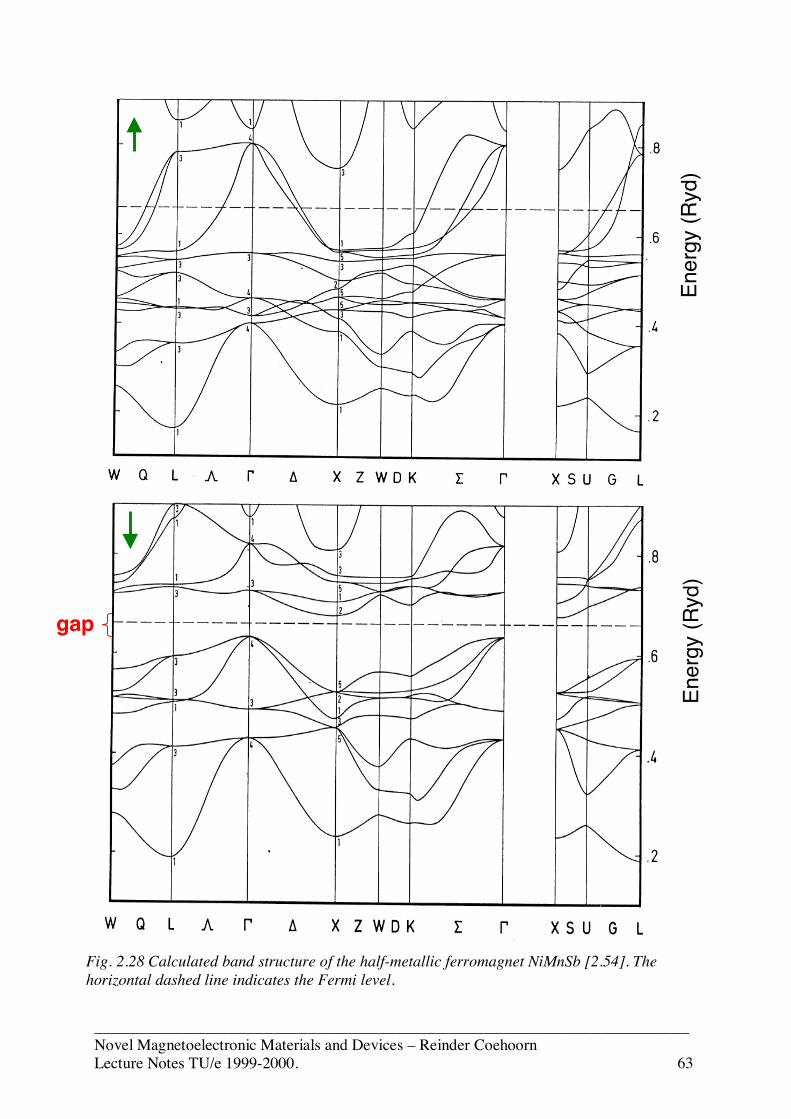
___________________________________________________________________Novel Magnetoelectronic Materials and Devices – Reinder CoehoornLecture Notes TU/e 1999-2000. 63
Fig. 2.28 Calculated band structure of the half-metallic ferromagnet NiMnSb [2.54]. Thehorizontal dashed line indicates the Fermi level.
Ener
gy (R
yd)
Ener
gy (R
yd)
gap
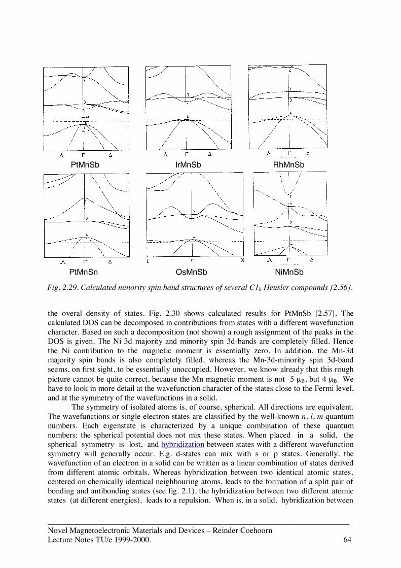
___________________________________________________________________Novel Magnetoelectronic Materials and Devices – Reinder CoehoornLecture Notes TU/e 1999-2000. 64
the overal density of states. Fig. 2.30 shows calculated results for PtMnSb [2.57]. Thecalculated DOS can be decomposed in contributions from states with a different wavefunctioncharacter. Based on such a decomposition (not shown) a rough assignment of the peaks in theDOS is given. The Ni 3d majority and minority spin 3d-bands are completely filled. Hencethe Ni contribution to the magnetic moment is essentially zero. In addition, the Mn-3dmajority spin bands is also completely filled, whereas the Mn-3d-minority spin 3d-bandseems, on first sight, to be essentially unoccupied. However, we know already that this roughpicture cannot be quite correct, because the Mn magnetic moment is not 5 µB, but 4 µB. Wehave to look in more detail at the wavefunction character of the states close to the Fermi level,and at the symmetry of the wavefunctions in a solid.
The symmetry of isolated atoms is, of course, spherical. All directions are equivalent.The wavefunctions or single electron states are classified by the well-known n, l, m quantumnumbers. Each eigenstate is characterized by a unique combination of these quantumnumbers: the spherical potential does not mix these states. When placed in a solid, thespherical symmetry is lost, and hybridization between states with a different wavefunctionsymmetry will generally occur. E.g. d-states can mix with s or p states. Generally, thewavefunction of an electron in a solid can be written as a linear combination of states derivedfrom different atomic orbitals. Whereas hybridization between two identical atomic states,centered on chemically identical neighbouring atoms, leads to the formation of a split pair ofbonding and antibonding states (see fig. 2.1), the hybridization between two different atomicstates (at different energies), leads to a repulsion. When is, in a solid, hybridization between
Fig. 2.29. Calculated minority spin band structures of several C1b Heusler compounds [2.56].
PtMnSb IrMnSb RhMnSb
PtMnSn OsMnSb NiMnSb
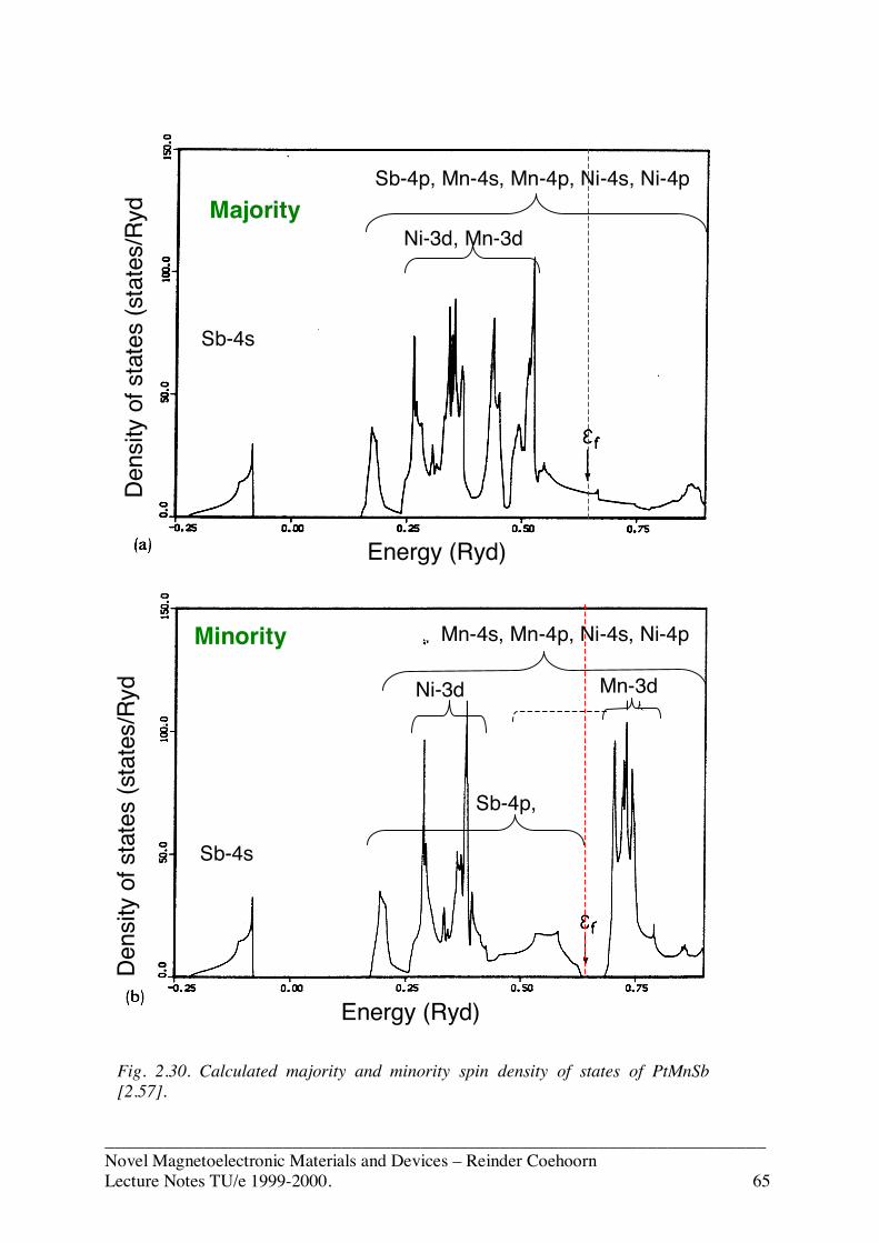
___________________________________________________________________Novel Magnetoelectronic Materials and Devices – Reinder CoehoornLecture Notes TU/e 1999-2000. 65
Fig. 2.30. Calculated majority and minority spin density of states of PtMnSb[2.57].
Dens
ity o
f sta
tes
(sta
tes/
Ryd
cell
spin
)
Energy (Ryd)
Dens
ity o
f sta
tes
(sta
tes/
Ryd
Energy (Ryd)
Majority
Minority
Sb-4s
Ni-3d, Mn-3d
Sb-4p, Mn-4s, Mn-4p, Ni-4s, Ni-4p
Sb-4s
Ni-3d Mn-3d
Mn-4s, Mn-4p, Ni-4s, Ni-4p
Sb-4p,
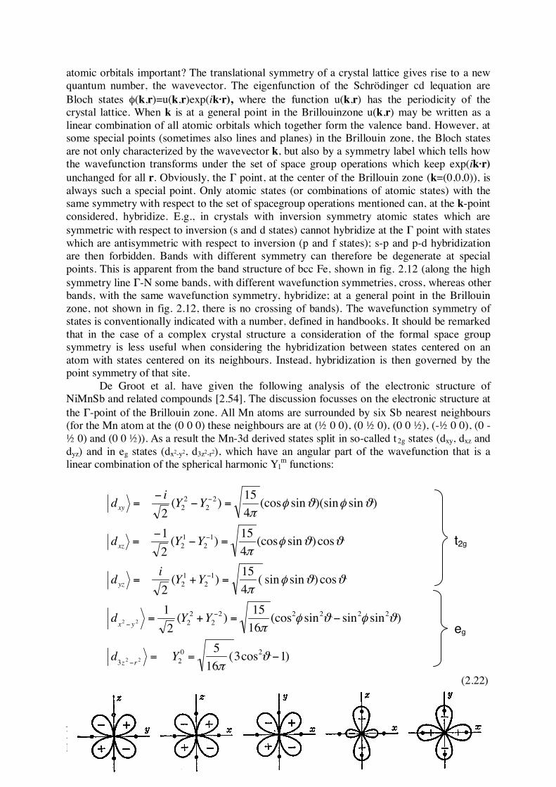
___________________________________________________________________Novel Magnetoelectronic Materials and Devices – Reinder CoehoornLecture Notes TU/e 1999-2000. 66
atomic orbitals important? The translational symmetry of a crystal lattice gives rise to a newquantum number, the wavevector. The eigenfunction of the Schrödinger cd lequation areBloch states φ(k,r)=u(k,r)exp(ik·r), where the function u(k,r) has the periodicity of thecrystal lattice. When k is at a general point in the Brillouinzone u(k,r) may be written as alinear combination of all atomic orbitals which together form the valence band. However, atsome special points (sometimes also lines and planes) in the Brillouin zone, the Bloch statesare not only characterized by the wavevector k, but also by a symmetry label which tells howthe wavefunction transforms under the set of space group operations which keep exp(ik·r)unchanged for all r. Obviously, the Γ point, at the center of the Brillouin zone (k=(0,0,0)), isalways such a special point. Only atomic states (or combinations of atomic states) with thesame symmetry with respect to the set of spacegroup operations mentioned can, at the k-pointconsidered, hybridize. E.g., in crystals with inversion symmetry atomic states which aresymmetric with respect to inversion (s and d states) cannot hybridize at the Γ point with stateswhich are antisymmetric with respect to inversion (p and f states); s-p and p-d hybridizationare then forbidden. Bands with different symmetry can therefore be degenerate at specialpoints. This is apparent from the band structure of bcc Fe, shown in fig. 2.12 (along the highsymmetry line Γ-N some bands, with different wavefunction symmetries, cross, whereas otherbands, with the same wavefunction symmetry, hybridize; at a general point in the Brillouinzone, not shown in fig. 2.12, there is no crossing of bands). The wavefunction symmetry ofstates is conventionally indicated with a number, defined in handbooks. It should be remarkedthat in the case of a complex crystal structure a consideration of the formal space groupsymmetry is less useful when considering the hybridization between states centered on anatom with states centered on its neighbours. Instead, hybridization is then governed by thepoint symmetry of that site.
De Groot et al. have given the following analysis of the electronic structure ofNiMnSb and related compounds [2.54]. The discussion focusses on the electronic structure atthe Γ-point of the Brillouin zone. All Mn atoms are surrounded by six Sb nearest neighbours(for the Mn atom at the (0 0 0) these neighbours are at (½ 0 0), (0 ½ 0), (0 0 ½), (-½ 0 0), (0 -½ 0) and (0 0 ½)). As a result the Mn-3d derived states split in so-called t2g states (dxy, dxz anddyz) and in eg states (dx2-y2, d3z2-r2), which have an angular part of the wavefunction that is alinear combination of the spherical harmonic Yl
m functions:
)1cos3(16
5
)sinsinsin(cos1615)(
21
cos)sinsin(415)(
2
cos)sin(cos415)(
21
)sin)(sinsin(cos415)(
2
2023
222222
22
12
12
12
12
22
22
22
22
−==
−=+=
=+=
=−−
=
=−−
=
−
−−
−
−
−
ϑπ
ϑφϑφπ
ϑϑφπ
ϑϑφπ
ϑφϑφπ
Yd
YYd
YYid
YYd
YYid
rz
yx
yz
xz
xy
(2.22)
t2g
eg
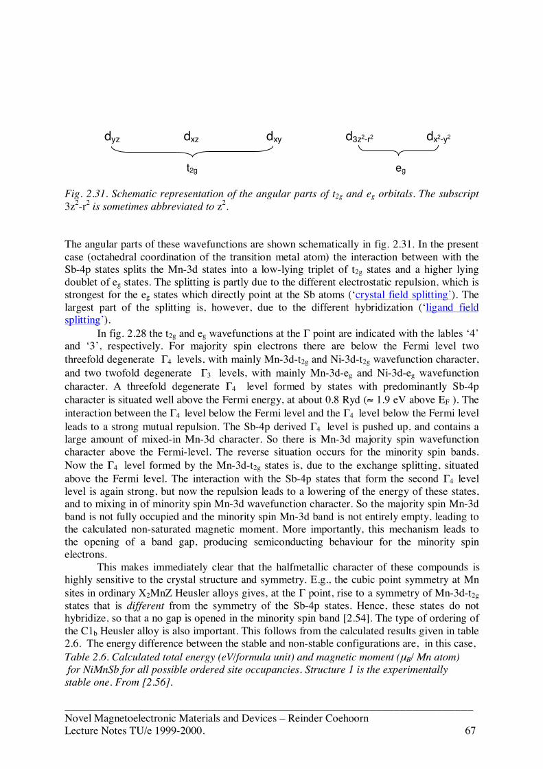
___________________________________________________________________Novel Magnetoelectronic Materials and Devices – Reinder CoehoornLecture Notes TU/e 1999-2000. 67
Fig. 2.31. Schematic representation of the angular parts of t2g and eg orbitals. The subscript3z2-r2 is sometimes abbreviated to z2.
The angular parts of these wavefunctions are shown schematically in fig. 2.31. In the presentcase (octahedral coordination of the transition metal atom) the interaction between with theSb-4p states splits the Mn-3d states into a low-lying triplet of t2g states and a higher lyingdoublet of eg states. The splitting is partly due to the different electrostatic repulsion, which isstrongest for the eg states which directly point at the Sb atoms (‘crystal field splitting’). Thelargest part of the splitting is, however, due to the different hybridization (‘ligand fieldsplitting’).
In fig. 2.28 the t2g and eg wavefunctions at the Γ point are indicated with the lables ‘4’and ‘3’, respectively. For majority spin electrons there are below the Fermi level twothreefold degenerate Γ4 levels, with mainly Mn-3d-t2g and Ni-3d-t2g wavefunction character,and two twofold degenerate Γ3 levels, with mainly Mn-3d-eg and Ni-3d-eg wavefunctioncharacter. A threefold degenerate Γ4 level formed by states with predominantly Sb-4pcharacter is situated well above the Fermi energy, at about 0.8 Ryd (≈ 1.9 eV above EF ). Theinteraction between the Γ4 level below the Fermi level and the Γ4 level below the Fermi levelleads to a strong mutual repulsion. The Sb-4p derived Γ4 level is pushed up, and contains alarge amount of mixed-in Mn-3d character. So there is Mn-3d majority spin wavefunctioncharacter above the Fermi-level. The reverse situation occurs for the minority spin bands.Now the Γ4 level formed by the Mn-3d-t2g states is, due to the exchange splitting, situatedabove the Fermi level. The interaction with the Sb-4p states that form the second Γ4 levellevel is again strong, but now the repulsion leads to a lowering of the energy of these states,and to mixing in of minority spin Mn-3d wavefunction character. So the majority spin Mn-3dband is not fully occupied and the minority spin Mn-3d band is not entirely empty, leading tothe calculated non-saturated magnetic moment. More importantly, this mechanism leads tothe opening of a band gap, producing semiconducting behaviour for the minority spinelectrons.
This makes immediately clear that the halfmetallic character of these compounds ishighly sensitive to the crystal structure and symmetry. E.g., the cubic point symmetry at Mnsites in ordinary X2MnZ Heusler alloys gives, at the Γ point, rise to a symmetry of Mn-3d-t2gstates that is different from the symmetry of the Sb-4p states. Hence, these states do nothybridize, so that a no gap is opened in the minority spin band [2.54]. The type of ordering ofthe C1b Heusler alloy is also important. This follows from the calculated results given in table2.6. The energy difference between the stable and non-stable configurations are, in this case,Table 2.6. Calculated total energy (eV/formula unit) and magnetic moment (µB/ Mn atom) for NiMnSb for all possible ordered site occupancies. Structure 1 is the experimentallystable one. From [2.56].
dyz dxz dxy d3z2-r2 dx2-y2
t2g eg
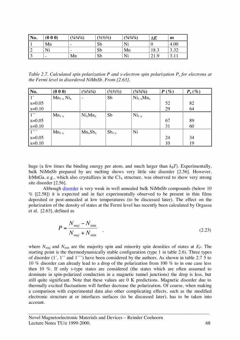
___________________________________________________________________Novel Magnetoelectronic Materials and Devices – Reinder CoehoornLecture Notes TU/e 1999-2000. 68
No. (0 0 0) (¼¼¼) (½½½) (¾¾¾) ΔE m1 Mn - Sb Ni 0 4.002 Ni - Sb Mn 18.3 3.323 - Mn Sb Ni 21.9 3.11
Table 2.7. Calculated spin polarization P and s-electron spin polarization Ps for electrons atthe Fermi level in disordered NiMnSb. From [2.63].
No. (0 0 0) (¼¼¼) (½½½) (¾¾¾) P (%) Ps (%)1’x=0.05x=0.10
Mn1-x Nix - Sb Ni1-xMnx 52 29
82 64
1’’x=0.05x=0.10
Mn1-x NixMnx Sb Ni1-x 67 31
89 60
1’’’x=0.05x=0.10
Mn1-x MnxSbx Sb1-x Ni 24 10
34 19
huge (a few times the binding energy per atom, and much larger than kBT). Experimentally,bulk NiMnSb prepared by arc melting shows very little site disorder [2.56]. However,IrMnGa, e.g., which also crystallizes in the C1b structure, was observed to show very strongsite disorder [2.56].
Although disorder is very weak in well annealed bulk NiMnSb compounds (below 10% [[2.58]) it is expected and in fact experimentally observed to be present in thin filmsdeposited or post-annealed at low temperatures (to be discussed later). The effect on thepolarization of the density of states at the Fermi level has recently been calculated by Orgassaet al. [2.63], defined as
min
min
NNNN
Pmaj
maj
+
−= , (2.23)
where Nmaj and Nmin are the majority spin and minority spin densities of states at EF. Thestarting point is the thermodynamically stable configuration (type 1 in table 2.6). Three typesof disorder (1’, 1’’ and 1’’’) have been considered by the authors. As shown in table 2.7 5 to10 % disorder can already lead to a drop of the polarization from 100 % to in one case lessthen 10 %. If only s-type states are considered (the states which are often assumed todominate in spin-polarized conduction in a magnetic tunnel junctions) the drop is less, butstill quite significant. Note that these values are 0 K predictions. Magnetic disorder due tothermally excited fluctuations will further decrease the polarization. Of course, when makinga comparison with experimental data also other complicating effects, such as the modifiedelectronic structure at or interfaces surfaces (to be discussed later), has to be taken intoaccount.

___________________________________________________________________Novel Magnetoelectronic Materials and Devices – Reinder CoehoornLecture Notes TU/e 1999-2000. 69
So far (full) substitutions of the non-magnetic atoms Ni and Sb by other non-magnetic atomshave, theoretically and experimentally, not led to the discovery of other HMFs. However,substitutions of Ni by other magnetic atoms, have led to interesting results. In fact, bandstructure calculations for all compounds of the type XMnSb, with X=Ni, Co, Fe, Mn and Crand with the crystal structure and site order of NiMnSb yield a halfmetallic ground state. Thepredicted magnetic moments are 4, 3, 2, 1 and 0 µB per formula unit. When going from Ni toCr the filling of the majority spin bands decreases, whereas the filling of the minority spinband remains the same. Apparently, the presence of the gap stabilizes the halfmetallicstructures. FeMnSb would be a halfmetallic ferrimagnet, with a sizeable Fe momentantiparallel to the Mn moment, and CrMnSb would even be a halfmetallic antiferromagnet. Itis a special antiferromagnet in the sense that the majority spin and minority spin densities ofstates are not identical, as for common antiferromagnets. See the density of states in fig. 2.32and 2.33. The material is better described as a fully compensated ferrimagnet, having amagnetic moment that is, due to the halfmetallic character, precisely equal to zero. Such ahalfmetallic antiferromagnet would be, if existing and if single domain, an very interestingmagnetoelectronic material. It would be a perfectly stable spin-polarized electrode in ajunction device, or as a tip in a spin-polarized STM which does not give rise to stray flux, andhence does not distort the domain structure of soft-magnetic systems to be studied.Unfortunately, CrMnSb does not crystallize in the ordered C1b crystal structure. However,these results show that such an important magnetoelectronic material could exist. Anoverview is given in table 2.8.
Table 2.8. Calculated and experimental properties of XMnSb compounds in the C1b structure.Magnetic moments per formula unit (total moment) and per atom [2.64].
Ref. Calculated magneticmoments (µB):Total,X, Mn, Sb,
Experiment
NiMnSb [2.54] 4,0.31, 3.74, -0.05
Stable ordered C1b
structure; m= 3.85 µB.CoMnSb [2.60] 3,
-0.09, 3.20, -0.11Disordered stucture (Co atoms partlyat empty sites); m= 3.93 µB.
FeMnSb [2.61] 2,-0.90, 2.94, -0.04
Compound does notexist. For partiallydisordered Ni1-xFexMnSbm extrapolates to 2.7 µB.
MnMnSb [2.59] 1-1.93, 2.94, -0.01
Compound crystallizes in anotherstructure.
CrMnSb [2.59,2.62]
0-2.35, 2.44, -0.09
Compound crystallizes in anotherstructure.
Van Leuken and de Groot have recently suggested a possible route towards ahalfmetallic antiferromagnet, viz. by making substitutions in the existing C1b type compoundVFeSb [2.59]. This compound is a non-magnetic semiconductor. It is isoelectronic with thenon-existing halfmetallic antiferromagnet CrMnSb. A 12.5 % substitution of Mn for V, and(in order to keep the system isoelectronic, In for Sb) was predicted to already yield
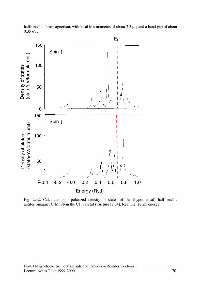
___________________________________________________________________Novel Magnetoelectronic Materials and Devices – Reinder CoehoornLecture Notes TU/e 1999-2000. 70
halfmetallic ferromagnetism, with local Mn moments of about 2.3 µ B and a band gap of about0.35 eV.
Fig. 2.32. Calculated spin-polarized density of states of the (hypothetical) halfmetallicantiferromagnet CrMnSb in the C1b crystal structure [2.64]. Red line: Fermi energy.
-0.4 -0.2 -0.0 0.2 0.4 0.6 0.8 1.0
Energy (Ryd)
Den
sity
of s
tate
s(s
tate
/eV/
form
ula
unit)
150
100
50
0
Den
sity
of s
tate
s(s
tate
/eV/
form
ula
unit)
150
100
50
0
EF
Spin ↑
Spin ↓
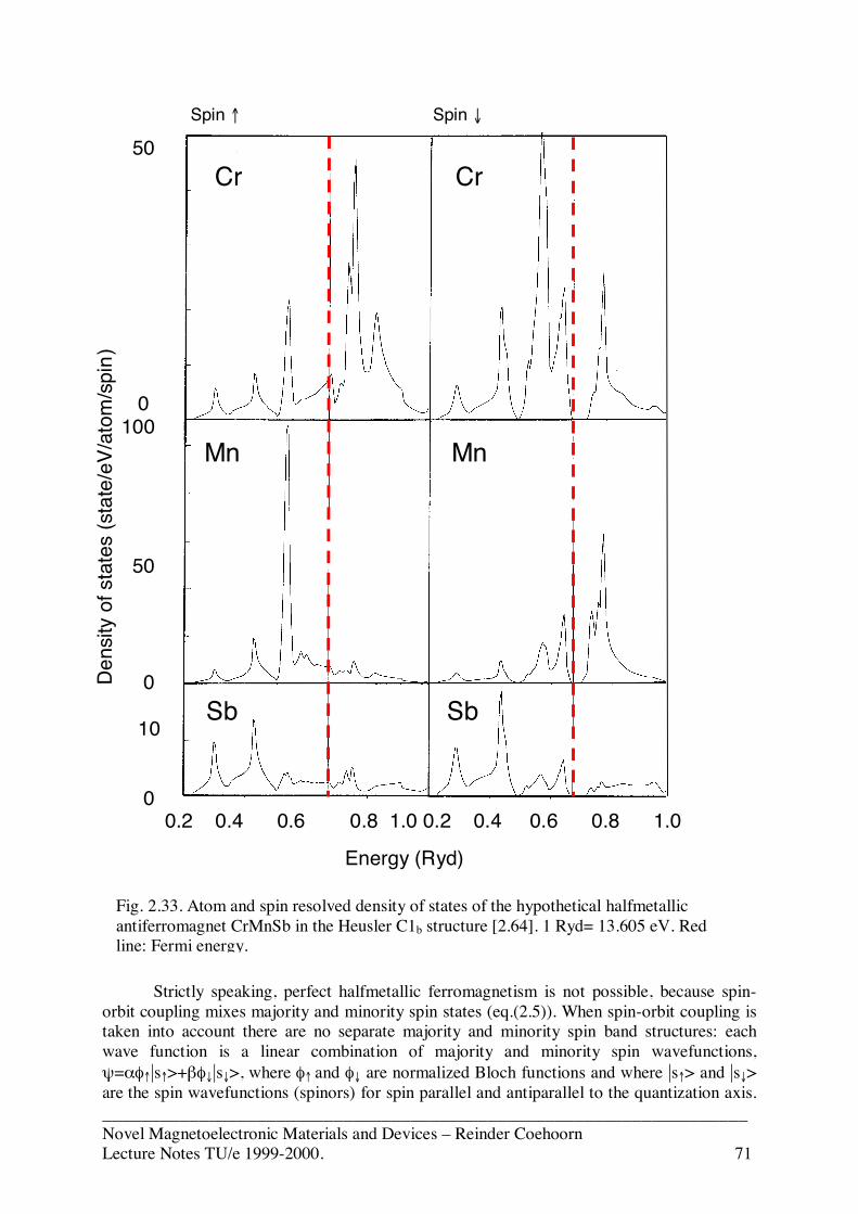
___________________________________________________________________Novel Magnetoelectronic Materials and Devices – Reinder CoehoornLecture Notes TU/e 1999-2000. 71
Strictly speaking, perfect halfmetallic ferromagnetism is not possible, because spin-orbit coupling mixes majority and minority spin states (eq.(2.5)). When spin-orbit coupling istaken into account there are no separate majority and minority spin band structures: eachwave function is a linear combination of majority and minority spin wavefunctions,ψ=αφ↑|s↑>+βφ↓|s↓>, where φ↑ and φ↓ are normalized Bloch functions and where |s↑> and |s↓>are the spin wavefunctions (spinors) for spin parallel and antiparallel to the quantization axis.
Spin ↑ Spin ↓
0.2 0.4 0.6 0.8 1.0 0.2 0.4 0.6 0.8 1.0
Energy (Ryd)
Den
sity
of s
tate
s (s
tate
/eV/
atom
/spi
n)
50
0 100
50
0
10
0
Cr Cr
Mn Mn
Sb Sb
Fig. 2.33. Atom and spin resolved density of states of the hypothetical halfmetallicantiferromagnet CrMnSb in the Heusler C1b structure [2.64]. 1 Ryd= 13.605 eV. Redline: Fermi energy.
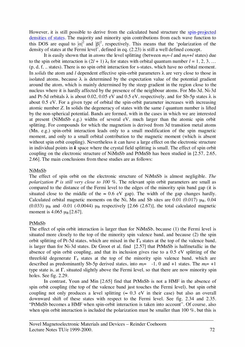
___________________________________________________________________Novel Magnetoelectronic Materials and Devices – Reinder CoehoornLecture Notes TU/e 1999-2000. 72
However, it is still possible to derive from the calculated band structure the spin-projecteddensities of states. The majority and minority spin contributions from each wave function tothis DOS are equal to |α|2 and |β|2, respectively. This means that the ‘polarization of thedensity of states at the Fermi level’, defined in eq. (2.23) is still a well defined concept.
It is easily shown that in atoms the level splitting (between ml=-l and ml=+l states) dueto the spin orbit interaction is (2l + 1) λl for states with orbital quantum number l = 1, 2, 3, …(p, d, f, .. states). There is no spin orbit interaction for s-states, which have no orbital moment.In solids the atom and l dependent effective spin-orbit parameters λ are very close to those inisolated atoms, because λ is determined by the expectation value of the potential gradientaround the atom, which is mainly determined by the steep gradient in the region close to thenucleus where it is hardly affected by the presence of the neighbour atoms. For Mn-3d, Ni-3dand Pt-5d orbitals λ is about 0.02, 0.05 eV and 0.5 eV, respectively, and for Sb-5p states λ isabout 0.5 eV. For a given type of orbital the spin-orbit parameter increases with increasingatomic number Z. In solids the degeneracy of states with the same l quantum number is liftedby the non-spherical potential. Bands are formed, with in the cases in which we are interestedat present (NiMnSb e.g.) widths of several eV, much larger than the atomic spin orbitsplitting. For compounds for which the magnetism is derived from 3d transition metal atoms(Mn, e.g.) spin-orbit interaction leads only to a small modification of the spin magneticmoment, and only to a small orbital contribution to the magnetic moment (which is absentwithout spin orbit coupling). Nevertheless it can have a large effect on the electronic structurein individual points in k space where the crystal field splitting is small. The effect of spin orbitcoupling on the electronic structure of NiMnSb and PtMnSb has been studied in [2.57, 2.65,2.66]. The main conclusions from these studies are as follows:
NiMnSbThe effect of spin orbit on the electronic structure of NiMnSb is almost negligible. Thepolarization P is still very close to 100 %. The relevant spin orbit parameters are small ascompared to the distance of the Fermi level to the edges of the minority spin band gap (it issituated close to the middle of the ≈ 0.6 eV gap). The width of the gap changes hardly.Calculated orbital magnetic moments on the Ni, Mn and Sb sites are 0.01 (0.017) µB, 0.04(0.033) µB and -0.01 (-0.0044) µB respectively [2.66 (2.67)], the total calculated magneticmoment is 4.065 µB [2.67].
PtMnSbThe effect of spin orbit interaction is larger than for NiMnSb, because (1) the Fermi level issituated more closely to the top of the minority spin valence band, and because (2) the spinorbit splitting of Pt-5d states, which are mixed in the Γ4 states at the top of the valence band,is larger than for Ni-3d states. De Groot et al. find [2.57] that PtMnSb is halfmetallic in theabsence of spin orbit coupling, and that its inclusion gives rise to a 0.5 eV splitting of thethreefold degenerate Γ4 states at the top of the minority spin valence band, which aredescribed as predominantly Sb-5p derived states, into ml= -1, 0 and +1 states. The ml= +1type state is, at Γ, situated slightly above the Fermi level, so that there are now minority spinholes. See fig. 2.29.
In contrast, Youn and Min [2.65] find that PtMnSb is not a HMF in the absence ofspin orbit coupling (the top of the valence band just touches the Fermi level), but spin orbitcoupling not only produces a level splitting (≈ 0.3 eV in their case) but also an overalldownward shift of these states with respect to the Fermi level. See fig. 2.34 and 2.35.“PtMnSb becomes a HMF when spin-orbit interaction is taken into account”. Of course, alsowhen spin orbit interaction is included the polarization must be smaller than 100 %, but this is
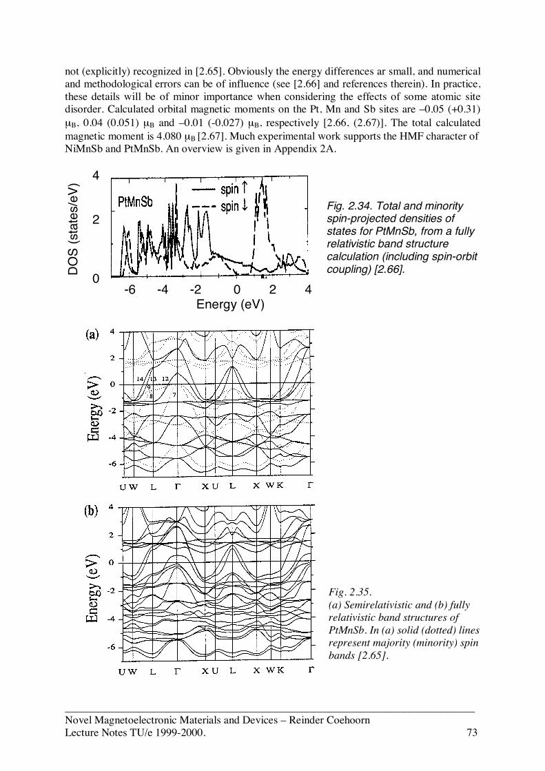
___________________________________________________________________Novel Magnetoelectronic Materials and Devices – Reinder CoehoornLecture Notes TU/e 1999-2000. 73
not (explicitly) recognized in [2.65]. Obviously the energy differences ar small, and numericaland methodological errors can be of influence (see [2.66] and references therein). In practice,these details will be of minor importance when considering the effects of some atomic sitedisorder. Calculated orbital magnetic moments on the Pt, Mn and Sb sites are –0.05 (+0.31)µB, 0.04 (0.051) µB and –0.01 (-0.027) µB, respectively [2.66, (2.67)]. The total calculatedmagnetic moment is 4.080 µB [2.67]. Much experimental work supports the HMF character ofNiMnSb and PtMnSb. An overview is given in Appendix 2A.
A.
-6 -4 -2 0 2 4 Energy (eV)
DO
S (s
tate
s/eV
) 4
2
0
Fig. 2.34. Total and minorityspin-projected densities ofstates for PtMnSb, from a fullyrelativistic band structurecalculation (including spin-orbitcoupling) [2.66].
Fig. 2.35.(a) Semirelativistic and (b) fullyrelativistic band structures ofPtMnSb. In (a) solid (dotted) linesrepresent majority (minority) spinbands [2.65].
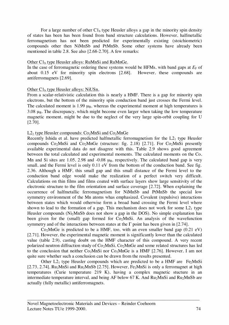
___________________________________________________________________Novel Magnetoelectronic Materials and Devices – Reinder CoehoornLecture Notes TU/e 1999-2000. 74
For a large number of other C1b type Heusler alloys a gap in the minority spin densityof states has been has been found from band structure calculations. However, halfmetallicferromagnetism has not been predicted for experimentally existing (stoichiometric)compounds other then NiMnSb and PtMnSb. Some other systems have already beenmentioned in table 2.8. See also [2.68-2.70]. A few remarks:
Other C1b type Heusler alloys: RuMnSi and RuMnGe.In the case of ferromagnetic ordering these systems would be HFMs, with band gaps at EF ofabout 0.15 eV for minority spin electrons [2.68]. However, these compounds areantiferromagnets [2.69].
Other C1b type Heusler alloys: NiUSn.From a scalar-relativistic calculation this is nearly a HMF. There is a gap for minority spinelectrons, but the bottom of the minority spin conduction band just crosses the Fermi level.The calculated moment is 1.99 µB, whereas the experimental moment at high temperatures is3.08 µB. The discrepancy, which might become even larger when taking the low temperaturemagnetic moment, might be due to the neglect of the very large spin-orbit coupling for U[2.70].
L21 type Heusler compounds: Co2MnSi and Co2MnGeRecently Ishida et al. have predicted halfmetallic ferromagnetism for the L21 type Heuslercompounds Co2MnSi and Co2MnGe (structure: fig. 2.18) [2.71]. For Co2MnSi presentlyavailable experimental data do not disagree with this. Table 2.9 shows good agreementbetween the total calculated and experimental moments. The calculated moments on the Co,Mn and Si sites are 1.05, 2.98 and -0.08 µB, respectively. The calculated band gap is verysmall, and the Fermi level is only 0.11 eV from the bottom of the conduction band. See fig.2.36. Although a HMF, this small gap and this small distance of the Fermi level to theconduction band edge would make the realization of a perfect switch very difficult.Calculations on thin films and films coated with surface layers show large sensitivity of theelectronic structure to the film orientation and surface coverage [2.72]. When explaining theoccurrence of halfmetallic ferromagnetism for NiMnSb and PtMnSb the special lowsymmetry environment of the Mn atoms whas emphasized. Covalent (repulsive) interactionsbetween states which would otherwise form a broad band crossing the Fermi level whereshown to lead to the formation of a gap. This mechanism does not work for some L21 typeHeusler compounds (Ni2MnSb does not show a gap in the DOS). No simple explanation hasbeen given for the (small) gap formed for Co2MnSi. An analysis of the wavefunctionsymmetry and of the interactions between states at the Γ point has been given in [2.74].
Co2MnGe is predicted to be a HMF, too, with an even smaller band gap (0.21 eV)[2.71]. However, the experimental magnetic moment is significantly lower than the calculatedvalue (table 2.9), casting doubt on the HMF character of this compound. A very recentpolarized neutron diffraction study of Co2MnSi, Co2MnGe and some related structures has ledto the conclusion that neither Co2MnSi nor Co2MnGe is a HMF [2.76]. However, I am notquite sure whether such a conclusion can be drawn from the results presented.
Other L21 type Heusler compounds which are predicted to be a HMF are Fe2MnSi[2.73, 2.74], Ru2MnSi and Ru2MnSb [2.75]. However, Fe2MnSi is only a ferromagnet at hightemperatures (Curie temperature 219 K), having a complex magnetic stucture in anintermediate temperature interval, and being AF below 67 K. And Ru2MnSi and Ru2MnSb areactually (fully metallic) antiferromagnets.
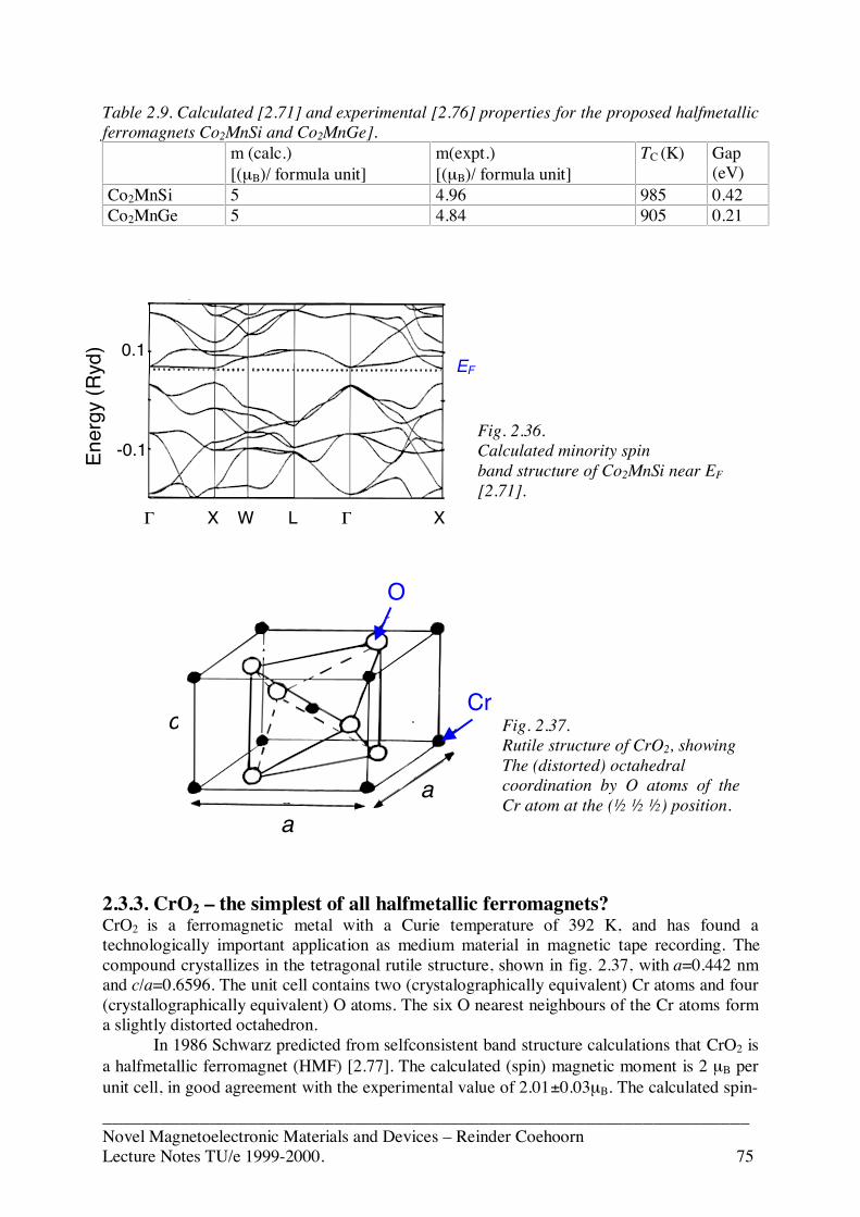
___________________________________________________________________Novel Magnetoelectronic Materials and Devices – Reinder CoehoornLecture Notes TU/e 1999-2000. 75
Table 2.9. Calculated [2.71] and experimental [2.76] properties for the proposed halfmetallicferromagnets Co2MnSi and Co2MnGe].
m (calc.)[(µB)/ formula unit]
m(expt.)[(µB)/ formula unit]
TC (K) Gap(eV)
Co2MnSi 5 4.96 985 0.42Co2MnGe 5 4.84 905 0.21
2.3.3. CrO2 – the simplest of all halfmetallic ferromagnets?CrO2 is a ferromagnetic metal with a Curie temperature of 392 K, and has found atechnologically important application as medium material in magnetic tape recording. Thecompound crystallizes in the tetragonal rutile structure, shown in fig. 2.37, with a=0.442 nmand c/a=0.6596. The unit cell contains two (crystalographically equivalent) Cr atoms and four(crystallographically equivalent) O atoms. The six O nearest neighbours of the Cr atoms forma slightly distorted octahedron.
In 1986 Schwarz predicted from selfconsistent band structure calculations that CrO2 isa halfmetallic ferromagnet (HMF) [2.77]. The calculated (spin) magnetic moment is 2 µB perunit cell, in good agreement with the experimental value of 2.01±0.03µB. The calculated spin-
Γ X W L Γ X
E
nerg
y (R
yd)
Fig. 2.36.Calculated minority spinband structure of Co2MnSi near EF[2.71].
EF
c
a
Cr
O
a
Fig. 2.37.Rutile structure of CrO2, showingThe (distorted) octahedralcoordination by O atoms of theCr atom at the (½ ½ ½) position.
0.1
-0.1
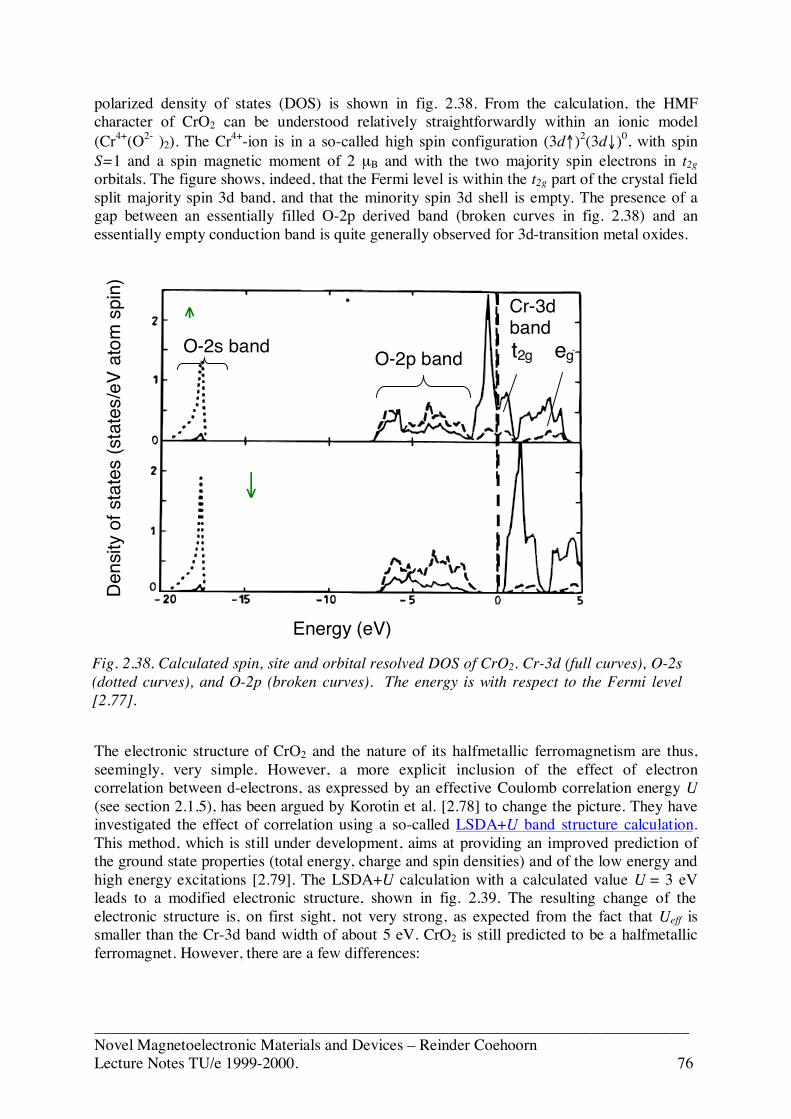
___________________________________________________________________Novel Magnetoelectronic Materials and Devices – Reinder CoehoornLecture Notes TU/e 1999-2000. 76
polarized density of states (DOS) is shown in fig. 2.38. From the calculation, the HMFcharacter of CrO2 can be understood relatively straightforwardly within an ionic model(Cr4+(O2- )2). The Cr4+-ion is in a so-called high spin configuration (3d↑)2(3d↓)0, with spinS=1 and a spin magnetic moment of 2 µB and with the two majority spin electrons in t2gorbitals. The figure shows, indeed, that the Fermi level is within the t2g part of the crystal fieldsplit majority spin 3d band, and that the minority spin 3d shell is empty. The presence of agap between an essentially filled O-2p derived band (broken curves in fig. 2.38) and anessentially empty conduction band is quite generally observed for 3d-transition metal oxides.
The electronic structure of CrO2 and the nature of its halfmetallic ferromagnetism are thus,seemingly, very simple. However, a more explicit inclusion of the effect of electroncorrelation between d-electrons, as expressed by an effective Coulomb correlation energy U(see section 2.1.5), has been argued by Korotin et al. [2.78] to change the picture. They haveinvestigated the effect of correlation using a so-called LSDA+U band structure calculation.This method, which is still under development, aims at providing an improved prediction ofthe ground state properties (total energy, charge and spin densities) and of the low energy andhigh energy excitations [2.79]. The LSDA+U calculation with a calculated value U = 3 eVleads to a modified electronic structure, shown in fig. 2.39. The resulting change of theelectronic structure is, on first sight, not very strong, as expected from the fact that Ueff issmaller than the Cr-3d band width of about 5 eV. CrO2 is still predicted to be a halfmetallicferromagnet. However, there are a few differences:
Energy (eV)
Den
sity
of s
tate
s (s
tate
s/eV
ato
m s
pin)
↑
↓
Fig. 2.38. Calculated spin, site and orbital resolved DOS of CrO2. Cr-3d (full curves), O-2s(dotted curves), and O-2p (broken curves). The energy is with respect to the Fermi level[2.77].
O-2p band
Cr-3d band t2g egO-2s band
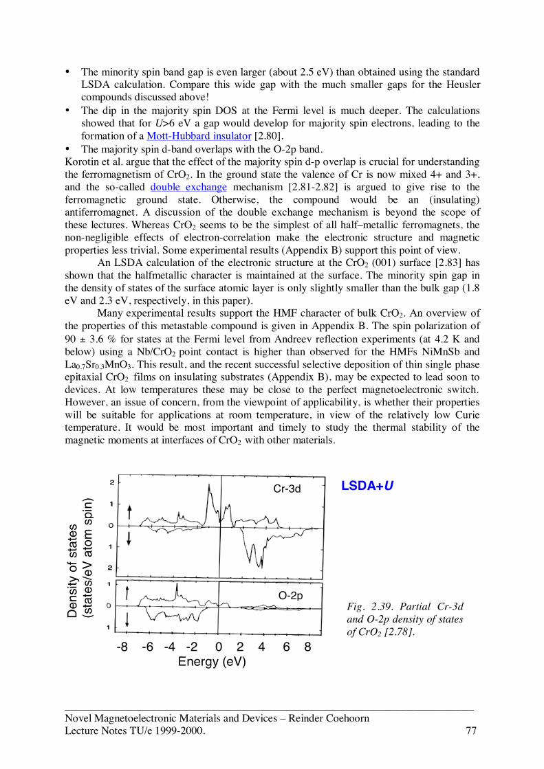
___________________________________________________________________Novel Magnetoelectronic Materials and Devices – Reinder CoehoornLecture Notes TU/e 1999-2000. 77
• The minority spin band gap is even larger (about 2.5 eV) than obtained using the standardLSDA calculation. Compare this wide gap with the much smaller gaps for the Heuslercompounds discussed above!
• The dip in the majority spin DOS at the Fermi level is much deeper. The calculationsshowed that for U>6 eV a gap would develop for majority spin electrons, leading to theformation of a Mott-Hubbard insulator [2.80].
• The majority spin d-band overlaps with the O-2p band.Korotin et al. argue that the effect of the majority spin d-p overlap is crucial for understandingthe ferromagnetism of CrO2. In the ground state the valence of Cr is now mixed 4+ and 3+,and the so-called double exchange mechanism [2.81-2.82] is argued to give rise to theferromagnetic ground state. Otherwise, the compound would be an (insulating)antiferromagnet. A discussion of the double exchange mechanism is beyond the scope ofthese lectures. Whereas CrO2 seems to be the simplest of all half–metallic ferromagnets, thenon-negligible effects of electron-correlation make the electronic structure and magneticproperties less trivial. Some experimental results (Appendix B) support this point of view.
An LSDA calculation of the electronic structure at the CrO2 (001) surface [2.83] hasshown that the halfmetallic character is maintained at the surface. The minority spin gap inthe density of states of the surface atomic layer is only slightly smaller than the bulk gap (1.8eV and 2.3 eV, respectively, in this paper).
Many experimental results support the HMF character of bulk CrO2. An overview ofthe properties of this metastable compound is given in Appendix B. The spin polarization of90 ± 3.6 % for states at the Fermi level from Andreev reflection experiments (at 4.2 K andbelow) using a Nb/CrO2 point contact is higher than observed for the HMFs NiMnSb andLa0.7Sr0.3MnO3. This result, and the recent successful selective deposition of thin single phaseepitaxial CrO2 films on insulating substrates (Appendix B), may be expected to lead soon todevices. At low temperatures these may be close to the perfect magnetoelectronic switch.However, an issue of concern, from the viewpoint of applicability, is whether their propertieswill be suitable for applications at room temperature, in view of the relatively low Curietemperature. It would be most important and timely to study the thermal stability of themagnetic moments at interfaces of CrO2 with other materials.
-8 -6 -4 -2 0 2 4 6 8 Energy (eV)
Cr-3d LSDA+U
Fig. 2.39. Partial Cr-3dand O-2p density of statesof CrO2 [2.78].
Den
sity
of s
tate
s(s
tate
s/eV
ato
m s
pin)
O-2p
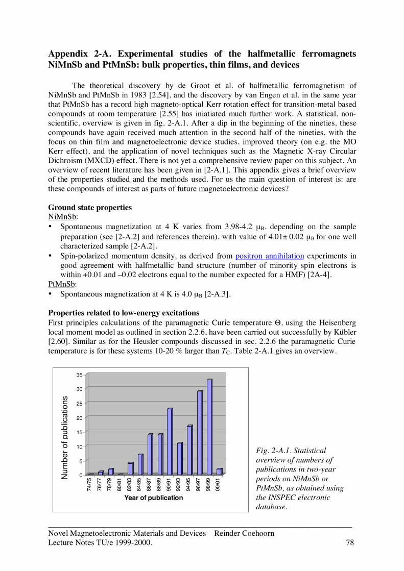
___________________________________________________________________Novel Magnetoelectronic Materials and Devices – Reinder CoehoornLecture Notes TU/e 1999-2000. 78
Appendix 2-A. Experimental studies of the halfmetallic ferromagnetsNiMnSb and PtMnSb: bulk properties, thin films, and devices
The theoretical discovery by de Groot et al. of halfmetallic ferromagnetism ofNiMnSb and PtMnSb in 1983 [2.54], and the discovery by van Engen et al. in the same yearthat PtMnSb has a record high magneto-optical Kerr rotation effect for transition-metal basedcompounds at room temperature [2.55] has iniatiated much further work. A statistical, non-scientific, overview is given in fig. 2-A.1. After a dip in the beginning of the nineties, thesecompounds have again received much attention in the second half of the nineties, with thefocus on thin film and magnetoelectronic device studies, improved theory (on e.g. the MOKerr effect), and the application of novel techniques such as the Magnetic X-ray CircularDichroism (MXCD) effect. There is not yet a comprehensive review paper on this subject. Anoverview of recent literature has been given in [2-A.1]. This appendix gives a brief overviewof the properties studied and the methods used. For us the main question of interest is: arethese compounds of interest as parts of future magnetoelectronic devices?
Ground state propertiesNiMnSb:• Spontaneous magnetization at 4 K varies from 3.98-4.2 µB, depending on the sample
preparation (see [2-A.2] and references therein), with value of 4.01± 0.02 µB for one wellcharacterized sample [2-A.2].
• Spin-polarized momentum density, as derived from positron annihilation experiments ingood agreement with halfmetallic band structure (number of minority spin electrons iswithin +0.01 and –0.02 electrons equal to the number expected for a HMF) [2A-4].
PtMnSb:• Spontaneous magnetization at 4 K is 4.0 µB [2-A.3].
Properties related to low-energy excitationsFirst principles calculations of the paramagnetic Curie temperature Θ, using the Heisenberglocal moment model as outlined in section 2.2.6, have been carried out successfully by Kübler[2.60]. Similar as for the Heusler compounds discussed in sec. 2.2.6 the paramagnetic Curietemperature is for these systems 10-20 % larger than TC. Table 2-A.1 gives an overview.
0
5
10
15
20
25
30
35
74/7
5
76/7
7
78/7
9
80/8
1
82/8
384
/85
86/8
7
88/8
9
90/9
192
/93
94/9
5
96/9
7
98/9
900
/01
Year of publication
Num
ber o
f pub
licat
ions
Fig. 2-A.1. Statisticaloverview of numbers ofpublications in two-yearperiods on NiMnSb orPtMnSb, as obtained usingthe INSPEC electronicdatabase.
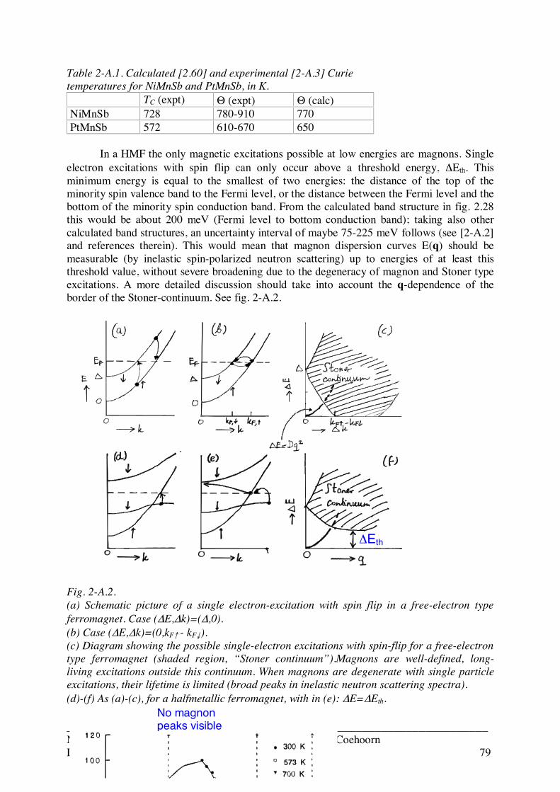
___________________________________________________________________Novel Magnetoelectronic Materials and Devices – Reinder CoehoornLecture Notes TU/e 1999-2000. 79
Table 2-A.1. Calculated [2.60] and experimental [2-A.3] Curietemperatures for NiMnSb and PtMnSb, in K.
TC (expt) Θ (expt) Θ (calc)NiMnSb 728 780-910 770PtMnSb 572 610-670 650
In a HMF the only magnetic excitations possible at low energies are magnons. Singleelectron excitations with spin flip can only occur above a threshold energy, ΔEth. Thisminimum energy is equal to the smallest of two energies: the distance of the top of theminority spin valence band to the Fermi level, or the distance between the Fermi level and thebottom of the minority spin conduction band. From the calculated band structure in fig. 2.28this would be about 200 meV (Fermi level to bottom conduction band); taking also othercalculated band structures, an uncertainty interval of maybe 75-225 meV follows (see [2-A.2]and references therein). This would mean that magnon dispersion curves E(q) should bemeasurable (by inelastic spin-polarized neutron scattering) up to energies of at least thisthreshold value, without severe broadening due to the degeneracy of magnon and Stoner typeexcitations. A more detailed discussion should take into account the q-dependence of theborder of the Stoner-continuum. See fig. 2-A.2.
Fig. 2-A.2.(a) Schematic picture of a single electron-excitation with spin flip in a free-electron typeferromagnet. Case (ΔE,Δk)=(Δ,0).(b) Case (ΔE,Δk)=(0,kF↑ - kF↓).(c) Diagram showing the possible single-electron excitations with spin-flip for a free-electrontype ferromagnet (shaded region, “Stoner continuum”).Magnons are well-defined, long-living excitations outside this continuum. When magnons are degenerate with single particleexcitations, their lifetime is limited (broad peaks in inelastic neutron scattering spectra).(d)-(f) As (a)-(c), for a halfmetallic ferromagnet, with in (e): ΔE=ΔEth.
ΔEth
No magnonpeaks visible
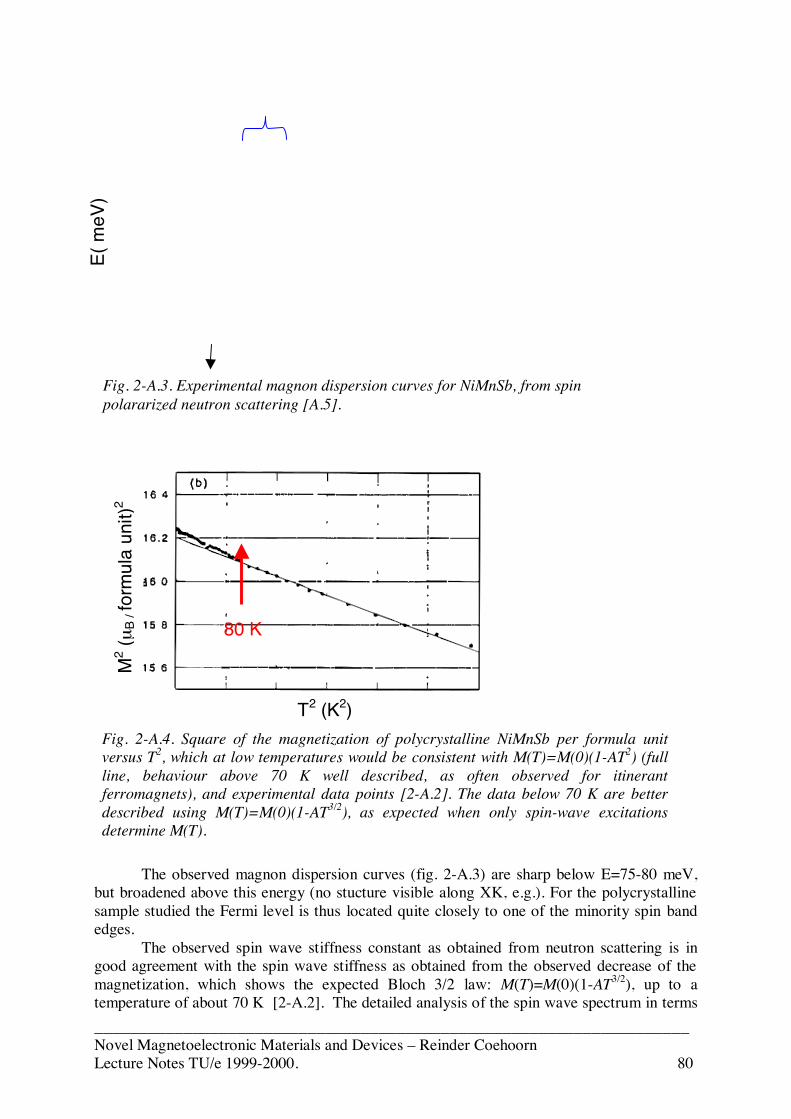
___________________________________________________________________Novel Magnetoelectronic Materials and Devices – Reinder CoehoornLecture Notes TU/e 1999-2000. 80
The observed magnon dispersion curves (fig. 2-A.3) are sharp below E=75-80 meV,but broadened above this energy (no stucture visible along XK, e.g.). For the polycrystallinesample studied the Fermi level is thus located quite closely to one of the minority spin bandedges.
The observed spin wave stiffness constant as obtained from neutron scattering is ingood agreement with the spin wave stiffness as obtained from the observed decrease of themagnetization, which shows the expected Bloch 3/2 law: M(T)=M(0)(1-AT3/2), up to atemperature of about 70 K [2-A.2]. The detailed analysis of the spin wave spectrum in terms
Fig. 2-A.3. Experimental magnon dispersion curves for NiMnSb, from spinpolararized neutron scattering [A.5].
Fig. 2-A.4. Square of the magnetization of polycrystalline NiMnSb per formula unitversus T2, which at low temperatures would be consistent with M(T)=M(0)(1-AT2) (fullline, behaviour above 70 K well described, as often observed for itinerantferromagnets), and experimental data points [2-A.2]. The data below 70 K are betterdescribed using M(T)=M(0)(1-AT3/2), as expected when only spin-wave excitationsdetermine M(T).
T2 (K2)
M2 (µ
B / fo
rmul
a un
it)2
E
( meV
)
80 K

___________________________________________________________________Novel Magnetoelectronic Materials and Devices – Reinder CoehoornLecture Notes TU/e 1999-2000. 81
of exchange constants J1 and J2 leads a value of the paramagnetic Curie temperature which isvery close to the (directly measured) experimental value and to the calculated value [2.60](see table 2-A.1). Also the separate experimental values of J1 and J2 are in good agreementwith the separately calculated values [2.60].
However, around the rather low temperature of 70 K the M(T) curve starts to deviatefrom the (1-AT3/2) form. In addition, resistivity measurements for bulk and thin film samplesreveal a discontinuity in the temperature derivative near 70-80 K. See figs. 2-A.4 and 2-A.5.This crossover at 70-80 K in the magnetization and resistivity curves is not yet understood.Hordequin [2-A.2] remarks: “It is observed for single crystals, polycrystalline samples, andmore or less ordered thin films, thus extrinsic origin must be ruled out, except if some fixed(sample independent) proportion of Mn or Ni goes into the vacancy sites”. Note that thetemperatures are much smaller than the temperature related to the threshold energy (80 meV,900-1000 K).
The resistivity measurements could be interpreted in terms of the opening of a newchannel for scattering around 70-80 K, may be as a result of the closing of the minority spingap, so that spin flip scattering would become possible. The fact that at higher temperaturesthe resistance curve does not show a T2 form, a form which is often taken as an indication ofspin-flip scattering, is not a counterargument against this, because the temperaturedependence of the contribution of spin flip scattering to the resistivity would depend in a non-trivial way on the temperature dependence of the threshold energy. However, it must bementioned that there is no experimental indication, from inelastic neutron scattering, that thethreshold energy changes considerably in the temperature range up to 300 K [2-A.2].
In summary:1. For NiMnSb and PtMnSb the local magnetic moment model provides a fair description of
the low-energy magnetic excitations.2. For NiMnSb the bottom of the minority spin conduction band is, at low temperatures,
about 80 meV above the Fermi level.
Fig. 2-A.5. Resistivity of bulk NiMnSb (lower curve) and of a thin film deposited at 573 K(upper curve). The continuous curve is a fit to the power law R=R0 + BT1.35 [2-A.2]. The isno a priori reason for expecting this power law, but the fit serves to make clear thatsomething happens around 70-80 K.
Temperature (K)
Res
istiv
ity (1
0-8 Ω
m)

___________________________________________________________________Novel Magnetoelectronic Materials and Devices – Reinder CoehoornLecture Notes TU/e 1999-2000. 82
3. The temperature dependences of the magnetization and the resistance show features at 70-80 K which have not yet been explained.
Research options:Temperature dependent measurement of the effective polarisation of tunnel junctions (with
NiMnSb as the cathode).Band structure calculations of NiMnSb with low-energy magnetically excited structures (such
as spin-spiral structures), to see what the effect is on the threshold energy.
Properties related to high-energy excitations (infrared, visible, UV, X-ray)
From infrared and visible light reflectance spectroscopy of NiMnSb films Mancoff etal. [A-2.6] have determined a rather sharp threshold energy, approximately 90 meV, abovewhich the scattering rate increases sharply. They have associated this with the onset of anadditional scattering channel which can be connected to spin-flip processes.
Fig. 2-A.6.(a) Reflectance spectrum for a500 nm NiMnSb film on saffire,at 300 K and at 80 K (inset),(b) Scattering rate spectrum,derived from the reflectancespectrum using a Kramers-Kronig analysis [2-A.6].
Wave number (cm-1 )
Scat
terin
g ra
te 1
/τ(ω
) (
cm-1
)
← Energy (eV)
← Energy (eV)
R
efle
ctan
ce R
(ω) (a)
(b)
300 K
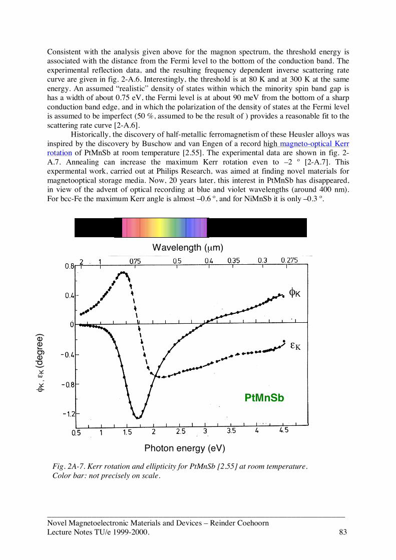
___________________________________________________________________Novel Magnetoelectronic Materials and Devices – Reinder CoehoornLecture Notes TU/e 1999-2000. 83
Consistent with the analysis given above for the magnon spectrum, the threshold energy isassociated with the distance from the Fermi level to the bottom of the conduction band. Theexperimental reflection data, and the resulting frequency dependent inverse scattering ratecurve are given in fig. 2-A.6. Interestingly, the threshold is at 80 K and at 300 K at the sameenergy. An assumed “realistic” density of states within which the minority spin band gap ishas a width of about 0.75 eV, the Fermi level is at about 90 meV from the bottom of a sharpconduction band edge, and in which the polarization of the density of states at the Fermi levelis assumed to be imperfect (50 %, assumed to be the result of ) provides a reasonable fit to thescattering rate curve [2-A.6].
Historically, the discovery of half-metallic ferromagnetism of these Heusler alloys wasinspired by the discovery by Buschow and van Engen of a record high magneto-optical Kerrrotation of PtMnSb at room temperature [2.55]. The experimental data are shown in fig. 2-A.7. Annealing can increase the maximum Kerr rotation even to –2 º [2-A.7]. Thisexpermental work, carried out at Philips Research, was aimed at finding novel materials formagnetooptical storage media. Now, 20 years later, this interest in PtMnSb has disappeared,in view of the advent of optical recording at blue and violet wavelengths (around 400 nm).For bcc-Fe the maximum Kerr angle is almost –0.6 º, and for NiMnSb it is only –0.3 º.
Photon energy (eV)
Wavelength (µm)
Fig. 2A-7. Kerr rotation and ellipticity for PtMnSb [2.55] at room temperature.Color bar: not precisely on scale.
PtMnSb
εK
φK
φ K , ε K
(deg
ree)
___________________________________________________________________Novel Magnetoelectronic Materials and Devices – Reinder CoehoornLecture Notes TU/e 1999-2000. 84
Similarly low values have been obtained for related Heusler compounds. The MOKerr effect is the result of the combination of the exchange splitting and the spin-orbitinteraction, which can give rise to a difference of the optical constants for left and rightcircularly polarized light (non-diagonal elements of the dielectric tensor). The large effect forPtMnSb led to the early belief that the special band structure of PtMnSb, with ml=1 holes inthe top of the minority spin valence band at the Γ point, was responsible for the large Kerrrotation [2.57]. Recent theoretical work on the Kerr effect in this and related compounds hasshown that the effect is not due to these holes, and that the HMF character of this compoundis not or only very indirectly relevant [2-A.8-10]. These recent publications show that goodprogress in being made on the theory of the magneto-optical Kerr effect, which (as any opticaleffect in the visible range) can only be understood when taking intraband as well as interbandexcitations into account. However, the focus on the energy scale above typically 1 eV makesthis work of less direct importance to the study of the detailed electronic structure near theFermi level. The magneto-optical Kerr effect in alloys and compounds is reviewed in [2-A.11].
Unlike optical spectroscopy, which suffers from the fact that neither the initial state orthe final state are obtained from the experiment (making some modelling necessary),photoelectron spectroscopy can, in principle, be used to obtain rather straightforwardlyinformation on the electronic structure. Upon photoemission of electrons by UV or X-rayphotons (of a fixed energy) electrons are emitted from the solid. The optical excitationprocess is energy-conserving, and this is also true for the transport of the photoelectron,provided that the excitation takes place within the escape depth (a few atomic layers, with formost substances a broad minimum of about 0.5 nm at electron energies around 100 eV). UVor X-ray photoelectron spectroscopy (UPS and XPS) are therefore surface-sensitivetechniques. The kinetic energy (Ekin) spectrum of the emitted photoelectrons can be related tothe spectrum of initial state energies (EI) by using Ei = Ekin – hν + Φ. Here hν and Φ are thephoton energy and the surface work function, respectively. The optical excitation process isalso spin-conserving, so when no spin flip takes place upon transport from the site ofexcitation to the vacuum, the spin of the initial state can also be measured. Finally, when asingle crystal is used, the conservation of momentum parallel to the surface plane (due to thetranslational variance of the system in this direction) can be used for extracting the k(parallel)wavevector in the initial state. The energy resolution is determined by the quality of the lightmonochromator and of the electron analyser. Although various photoemission studies havebeen performed [2-A.12], none of them have given specific information about the spinpolarization at the Fermi level, or the width of the minority spin band gap.
Bona et al. have applied a variant of this technique, photothreshold emissionspectroscopy, to polycrystalline magnetically saturated NiMnSb: as a function of the photon-energy the spin-resolved energy integrated intensity of photoelectrons was measured, forphoton energies just above the surface work function (energy range hν= 4.5-5.4 eV) [2-A.13].Electrons with a kinetic energy smaller than the energy difference between the top of thevalence band and the Fermi level are expected to be +100 % spin polarized. From fig. 2.28this should be so for kinetic energies below about 0.4 eV. The emitted electrons are expectedto have an escape depth (average perpendicular component of the inelastic mean free path) ofthe order 5 nm, so that the experiment is not extremely sensitive to surface disorder. However,even in this case zero polarisation for emission from the first unit cell (0.6 nm) would alreadyreduce the polarization to 89 %, if the polarization from the bulk were 100 % [2-A.12]. Infact, the authors indirectly, by Auger analysis of Ni and Mn, some surface segregation of Sb.
izat
ion
(%)

___________________________________________________________________Novel Magnetoelectronic Materials and Devices – Reinder CoehoornLecture Notes TU/e 1999-2000. 85
The result obtained is shown in fig. 2-A.8. The largest observed polarization is about50 %. After careful analysis of a number of factors which play a role (escape depth, possiblespin depolarization at the surface) the authors conclude that the energy gap in the density ofstates is certainly smaller than 0.5 eV. It is noted that they seem to mean, from their fig. 1,that in fact the distance between the top of the minority spin valence band and the Fermi levelis less then 0.25 eV (instead of the calculated 0.4 eV). NiMnSb and PtMnSb have also been studied using X-ray Magnetic CircularDichroism [2-A.14], a technique within which the circular polarization dependence of the X-ray absorption due to spin-orbit split core levels is measured. From its analysis atom-resolvedmagnetic spin and orbital moments can be derived. So, although this may seem a bitparadoxical for a techniques which involves high-energy excitations, XMCD providesground-state information. The results obtained are consistent with the theoretical andexperimental results presented above and in the main text of this chapter. No detailedinformation about the minority spin gap has been obtained.
Thin films and multilayersThin film and multilayer studies have been motivated by the prospects of recordingapplications of the high MO Kerr effect of PtMnSb, and of magnetoelectronic deviceapplications, for which NiMnSb is the more appropriate candidate. Conversely, the Kerrrotation has also been used for judging the quality of the films. Issues are composition,structural order and surface segregation.
Important results / highlights on the way to possible magnetoelectronic deviceapplications:• First successful deposition of NiMnSb films by evaporation onto heated glass or sapphire.
Moodera group MIT, 1990 [2-A.15].• Deposition of epitaxial PtMnSb and NiMnSb by dc magnetron cosputtering on
sapphire(0001), White group Stanford, 1997 [2-A.16].• Rf magnetron sputtering from a single composite target, 250-350 ºC, no post anneal, layer
thickness 10 nm, lowest resistivity 65 ×10-8 Ωm, Childress group, Florida [2-A.17].• Sputter deposited NiMnSb films with MO Kerr rotation and ellipticity very close to the
bulk spectra [2-A.18]. “Magnetotransport and tunneling experiments being developed”.Florida, Orsay, IBM Almaden collaboration.
Fig. 2-A.8. Measuredelectron spinpolarization P versusphoton energy forNiMnSb at roomtemperature (dots andcrosses) and 20 K ( )[2-A.13].Φ is the workfunction energy.
Photon energy (eV)
Φ
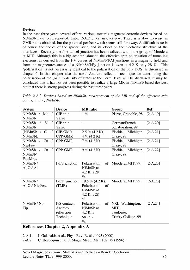
___________________________________________________________________Novel Magnetoelectronic Materials and Devices – Reinder CoehoornLecture Notes TU/e 1999-2000. 86
DevicesIn the past three years several efforts various towards magnetoelectronic devices based onNiMnSb have been reported. Table 2-A.2 gives an overview. There is a slow increase inGMR ratios obtained, but the potential perfect switch seems still far away. A difficult issue isof course the choice of the spacer layer, and its effect on the electronic structure of theinterfaces. Recently, the first tunnel junction has been realized, within the group of Mooderaat MIT. Although this is a big accomplishment, the effective spin polarization of tunnelingelectrons, as derived from the I-V curves of NiMnSb/I/Al junctions in a magnetic field andfrom the magnetoresistance of a NiMnSb/I/Py junction is even at 4.2 K only 28 %. This‘polarization’ is not necessarily identical to the polarisation of the bulk DOS, as discussed inchapter 6. In that chapter also the novel Andreev reflection technique for determining thepolarisation of the (or a ?) density of states at the Fermi level will be discussed. It may beconcluded that it has not yet been possible to realize a large MR in NiMnSb based devices,but that there is strong progress during the past three years.
Table 2-A.2. Devices based on NiMnSb: measurement of the MR and of the effective spinpolarization of NiMnSb.
System Device MR ratio Group Ref.NiMnSb / Mo /NiMnSb
CIP spinValve
1 % Pierre, Grenoble, 98 [2-A.19]
NiMnSb / V /NiMnSb
CIP spinValve
- German/Frenchcollaboration, 99
[2-A.20]
(NiMnSb / Cu /NiMnSb)n
CIP-GMRCPP-GMR
2.5 % (4.2 K)4 % (4.2 K)
Florida, Michigan,Orsay, 98
[2-A.21]
NiMnSb / Cu /Ni80Fe20
CPP-GMR 7 % (4.2 K) Florida, Michigan,Orsay, 98
[2-A.21]
NiMnSb / Cu /NiMnSb/Fe50Mn50
CPP-GMR 9 % (4.2 K) Florida, Michigan,Orsay, 99
[2-A.22]
NiMnSb /Al2O3/ Al
F/I/S junction Polarisation ofNiMnSb at4.2 K is 28%.
Moodera, MIT, 99. [2-A.23]
NiMnSb /Al2O3/ Ni80Fe20
F/I/F junction(TMR)
19.5 % (4.2 K).Polarisation ofNiMnSb at4.2 K is 28%.
Moodera, MIT, 99. [2-A.23]
NiMnSb / Nb-Tip
F/S contact,AndreevreflectionTechnique
Polarisation ofNiMnSb at4.2 K is58±2.3%.
NRL, Washington,MIT,Toulouse,Trinity College, 99
[2-A.24]
References Chapter 2, Appendix A
2-A.1. I. Galanakis et al., Phys. Rev. B. 61, 4093 (2000).2-A.2. C. Hordequin et al. J. Magn. Magn. Mat. 162, 75 (1996).
___________________________________________________________________Novel Magnetoelectronic Materials and Devices – Reinder CoehoornLecture Notes TU/e 1999-2000. 87
2-A.3. M.J. Otto et al., J. Phys. Cond. Matt. 1, 2341 (1989).2-A.4. K.E.H.M. Hanssen et al., Phys. Rev. B34, 5009 (1986); Phys. Rev. B42, 1533
(1990).2-A.5. C. Hordequin et al., Physica B 234-236, 605 (1997).2-A.6. F.B. Mancoff et al., Phys. Rev. B 60, R12565 (1999).2-A.7. K. Takanashi et al., Jpn. J. Appl. Phys. 27, L2351 (1988).2-A.8. J. van Ek and J.M. Maclaren, Phys. Rev. B 56, R2924 (1997).2-A.9. V.N. Antonov et al., Phys. Rev. 56, 13012 (1997).2-A.10. Xiang Gao et al., Phys. Rev. 59, 9965 (1999).2-A.11. K.H.J. Buschow, “Magneto-optical properties of alloys and intermetallic
compounds”, in Handbook of Magnetic Materials, Vol.4, ed. K.H.J. Buschow, p.493- , North-Holland, Amsterdam (19xx).
2-A.12. See e.g. E. Kisker et al., J. Magn. Magn. Mat. 70, 21 (1987), J.-S. Kang et al., SolidState Comm. 88, 653 (1993).
2-A.13. G.L. Bona et al., Solid State Comm. 56, 391 (1985).2-A.14. A. Kimura et al., J. Electron Spectr. and Rel. Phen. 78, 287 (1996); A. Kimura et
al., Phys. Rev. B 56, 6021 (1997); S. Suga and S. Imada, J. Electron Spectr. andRel. Phen. 92, 1 (1998);
2-A.15. R. Kabani et al., J. Appl. Phys. 67, 4898 (1990).2-A.16. J.F. Bobo et al., J. Appl. Phys. 81, 4164 (1997).2-A.17. J.A. Caballero et al., J. Appl. Phys. 81, 2740 (1997).2-A.18. J. A. Caballero et al., Appl. Phys. Lett. 71, 2382 (1997); J. Magn. Magn. Mat. 177,
1229 (1998).2-A.19. C. Hordequin, J. Magn. Magn. Mat. 183, 225 (1998).2-A.20. J.-P. Schlomka et al, J. Appl. Phys. 86, 5146 (1999).2-A.21. J.A. Caballero et al., J. Vac. Sc. Techn. A16, 1801 (1998).2-A.22. J.A. Caballero et al., J. Magn. Magn. Mat. 198, 55 (1999).2-A.23. C.T. Tanaka et al., J. Appl. Phys. 1997, 5515 (1997); J. Appl. Phys. 86, 6239
(1999).2-A.24. R.J. Soulen et al., Science 282, 85 (1998); J. Appl. Phys. 85, 4589 (1999).
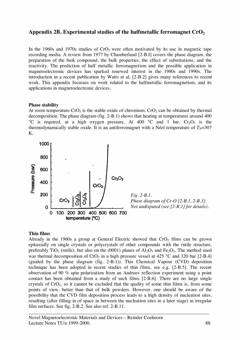
___________________________________________________________________Novel Magnetoelectronic Materials and Devices – Reinder CoehoornLecture Notes TU/e 1999-2000. 88
Appendix 2B. Experimental studies of the halfmetallic ferromagnet CrO2
In the 1960s and 1970s studies of CrO2 were often motivated by its use in magnetic taperecording media. A review from 1977 by Chamberland [2-B.I] covers the phase diagram, thepreparation of the buik compound, the bulk properties, the effect of substitutions, and thereactivity. The prediction of half metallic ferromagnetism and the possible application inmagnetoelectronic devices has sparked renewed interest in the 1980s and 1990s. Theintroduction in a recent publication by Watts et al. [2-B.2] gives many references to recentwork. This appendix focusses on work related to the halfmetallic ferromagnetism, and itsapplications in magnetoelectronic devices.
Phase stabilityAt room temperature CrO3 is the stable oxide of chromium. CrO2 can be obtained by thermaldecomposition. The phase diagram (fig. 2-B.1) shows that heating at temperatures around 400°C is required, at a high oxygen pressure. At 400 °C and 1 bar, Cr2O3 is thethermodynamically stable oxide. It is an antiferromagnet with a Néel temperature of TN=307K.
Thin filmsAlready in the 1960s a group at General Electric showed that CrO2 films can be grownepitaxially on single crystals or polycrystals of other compounds with the rutile structure,preferably TiO2 (rutile), but also on the (0001) planes of Al2O3 and Fe2O3. The method usedwas thermal decomposition of CrO3 in a high pressure vessel at 425 °C and 320 bar [2-B.4](guided by the phase diagram (fig. 2-B.1)). This Chemical Vapour (CVD) depositiontechnique has been adopted in recent studies of thin films, see e.g. [2-B.5]. The recentobservation of 90 % spin polarization from an Andreev reflection experiment using a pointcontact has been obtained from a study of such films [2-B.6]. There are no large singlecrystals of CrO2, so it cannot be excluded that the quality of some thin films is, from somepoints of view, better than that of bulk powders. However, one should be aware of thepossibility that the CVD film deposition process leads to a high density of nucleation sites,resulting (after filling in of space in between the nucleation sites in a later stage) in irregularfilm surfaces. See fig. 2-B.2. See also ref. 2-B.11.
Fig. 2-B.1.Phase diagram of Cr-O [2-B.1, 2-B.3].Not undisputed (see [2-B.1] for details).
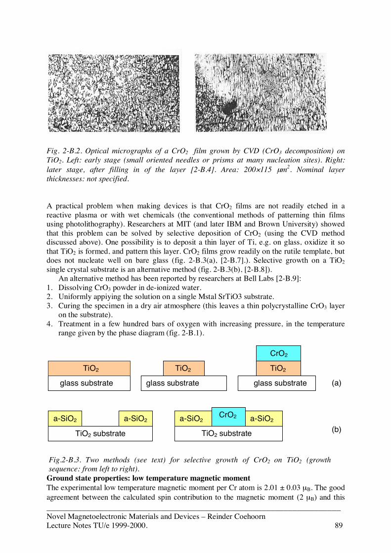
___________________________________________________________________Novel Magnetoelectronic Materials and Devices – Reinder CoehoornLecture Notes TU/e 1999-2000. 89
Fig. 2-B.2. Optical micrographs of a CrO2 film grown by CVD (CrO3 decomposition) onTiO2. Left: early stage (small oriented needles or prisms at many nucleation sites). Right:later stage, after filling in of the layer [2-B.4]. Area: 200×115 µm2. Nominal layerthicknesses: not specified.
A practical problem when making devices is that CrO2 films are not readily etched in areactive plasma or with wet chemicals (the conventional methods of patterning thin filmsusing photolithography). Researchers at MIT (and later IBM and Brown University) showedthat this problem can be solved by selective deposition of CrO2 (using the CVD methoddiscussed above). One possibility is to deposit a thin layer of Ti, e.g. on glass, oxidize it sothat TiO2 is formed, and pattern this layer. CrO2 films grow readily on the rutile template, butdoes not nucleate well on bare glass (fig. 2-B.3(a), [2-B.7].). Selective growth on a TiO2single crystal substrate is an alternative method (fig. 2-B.3(b), [2-B.8]).
An alternative method has been reported by researchers at Bell Labs [2-B.9]:1. Dissolving CrO3 powder in de-ionized water.2. Uniformly appiying the solution on a single Mstal SrTiO3 substrate.3. Curing the specimen in a dry air atmosphere (this leaves a thin polycrystalline CrO3 layer
on the substrate).4. Treatment in a few hundred bars of oxygen with increasing pressure, in the temperature
range given by the phase diagram (fig. 2-B.1).
Ground state properties: low temperature magnetic momentThe experimental low temperature magnetic moment per Cr atom is 2.01 ± 0.03 µB. The goodagreement between the calculated spin contribution to the magnetic moment (2 µB) and this
glass substrate glass substrate glass substrate
TiO2 TiO2 TiO2
CrO2
(a)
TiO2 substrate
a-SiO2 a-SiO2
TiO2 substrate
a-SiO2 a-SiO2 CrO2
(b)
Fig.2-B.3. Two methods (see text) for selective growth of CrO2 on TiO2 (growthsequence: from left to right).

___________________________________________________________________Novel Magnetoelectronic Materials and Devices – Reinder CoehoornLecture Notes TU/e 1999-2000. 90
(total) experimental magnetic moment per Cr atom suggests that the orbital magnetic momentis almost fully quenched by the crystal field. X-ray Magnetic Circular Dichroism experimentshave confirmed this: the orbital moment is at most 0.01 µB [2.B.10]. The experimentallyconfirmed integer value of the magnetic moment provides strong support to the view thatCrO2 is a half-metallic ferromagnet.
Properties related to low-energy excitationsSpecific heat
Barry et al. [2-B.11] have measured the specific beat, C, of a commercial CrO2powder, and fitted the results below 15 K to the expression C= γT+ βT3+ αT3/2, where thethree terms represent the electron, phonon and magnon contributions, respectively (seetextbooks, e.g. Kittel [2.1]). Assuming Cel= γT=(1/3)π2N(EF)kBT, which is valid for a gas ofindependent (non-interacting) electrons the experimental value γ=5.1(9) mJ/mol K2 leads toN(EF)=2.2 states/eV atom, much larger than the experimental results of about 0.5 states/eVatom, or even less, obtained by Schwarz or by Korotin et al. (figs. 2.38 and 2.39). (Anexperimental value γ= 7 mJ/mol K2 is quoted in [2-B.12]). The value of γ can be enhanced bya factor (1+λ,) due to the electron-phonon interaction. For non-magnetic metalssuperconductivity can occur when the enhancement is large. An electron-phononenhancement parameter λ>l is considered to be extremely unlikely for CrO2; this discrepancybetween theory and experiment is regarded as an indication that the specific heat enhancementis due to electron correlation, beyond the LSDA [2-B.12].Magnetization at finite temperatures
Up to at least 100 K the magnetization is found to be described by the Bloch T3/2 law:M(T)=M(O)(1 - BT3/2). The parameter B is inversely proportional to the spin wave stiffnessconstant D, leading to D=150 meV A2 [2-B.12]. No results of inelastic neutron scatteringexperiments, which could give an indication of the energy above which magnons becomedegenerate with single-electron excitations (see Appendix 2A, NiMnSb), have been reported.Such experiments would be extremely interesting. In addition, a theoretical effort to predictthe spin wave stiffness constant from band structure calculations would be of great interest, inparticular in view of the ideas put forward on the origin of the ferromagnetic ground state putforward by Korotin et al. (see the main text).Resistivity
Much experimental work and some theoretical analysis has been done on theresistivity of bulk samples and thin films. Only a selection of the thin film results will bediscussed. Fig. 2-B.4 gives the bulk resistivity, compared with that for Ni and Nb. CrO2 is afairly good metal at low temperatures, but has a very high resistivity at room temperature, ascompared to a more ordinary ferromagnetic metal such as Ni. lt is therefore often called a“bad metal”. For the magnetic metals CrO2 and Ni an additional contribution to the resistivityis evident, which may be ascribed to spin flip scattering. From the experimental data,combined with calculated Fermi surfaces, Lewis et al. [2-B.12] have derived an effectiveaverage mean free path for electrons in CrO2 of 1.4 nm at 300 K, and 70 nm at 5 K. lt is notyet clear how the very high resistance at room temperature can be explained, and how thismay be related to the halfmetallic character. Barry et al. [2-B.11] and Watts et al. [2-B.2] havefound that, phenomenologically, the resistivity is well described by the expression ρ(T)=ρ0+αT2 exp(-Δ/kT), with Δ/k≈80 K (Δ= 5-10 meV). A T2 term in the resistivity is often attributedto electron-magnon scattering, and the exponential factor in this term could be interpreted asthe result of suppression of electron-magnon scattering due to the presence of a gap of energyΔ in the electron-magnon spectrum [2-B.2]. Although there is clearly a large gap at T=0 in the
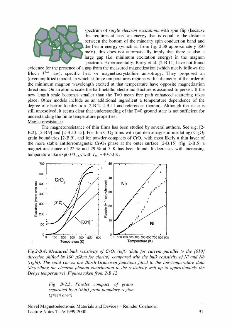
___________________________________________________________________Novel Magnetoelectronic Materials and Devices – Reinder CoehoornLecture Notes TU/e 1999-2000. 91
spectrum of single electron excitations with spin flip (becausethis requires at least an energy that is equal to the distancebetween the bottom of the minority spin conduction band andthe Fermi energy (which is, from fig. 2.38 approximately 350meV), this does not automatically imply that there is also alarge gap (i.e. minimum excitation energy) in the magnonspectrum. Experimentally, Barry et al. [2-B.11] have not found
evidence for the presence of a gap from the measured magnetization (which nicely follows theBloch T3/2 law), specific heat or magnetiocrystalline anisotropy. They proposed an(oversimplified) model, in which at finite temperatures regions with a diameter of the order ofthe minimum magnon wavelength excited at that temperature have opposite magnetizationdirections. On an atomic scale the halfmetallic electronic stucture is assumed to persist. If thenew length scale becomes smaller than the T=0 mean free path enhanced scattering takesplace. Other models include as an additional ingredient a temperature dependence of thedegree of electron localization [2-B.2, 2-B.11 and references therein]. Although the issue isstill unresolved, it seems clear that understanding of the T=0 ground state is not sufficient forunderstanding the finite temperature properties.Magnetoresistance
The magnetoresistance of thin films has been studied by several authors. See e.g. [2-B.2], [2-B.9] and [2-B.13-15]. For thin CrO2 films with (antiferromagnetic insulating) Cr2O3grain boundaries [2-B.9], and for powder compacts of CrO2 with most likely a thin layer ofthe more stable antiferromagnetic Cr2O3 phase at the outer surface [2-B.15] (fig. 2-B.5) amagnetoresistance of 22 % and 29 % at 5 K has been found. It decreases with increasingtemperature like exp(-T/Tmr), with Tmr ≈ 40-50 K.
Fig.2-B.4. Measured buik resistivity of CrO2 (left) (data for current parallel to the [010]direction shifted by 100 µΩcm for clarity), compared with the bulk resistivity of Ni and Nb(right). The solid curves are Bloch-Grüneisen functions fitted to the low-temperature data(describing the electron-phonon contribution to the resistivity weil up to approximately theDebye temperature). Figures taken from 2-B.12.
Fig. B-2.5. Powder compact, of grainsseparated by a (thin) grain boundary region(green area).
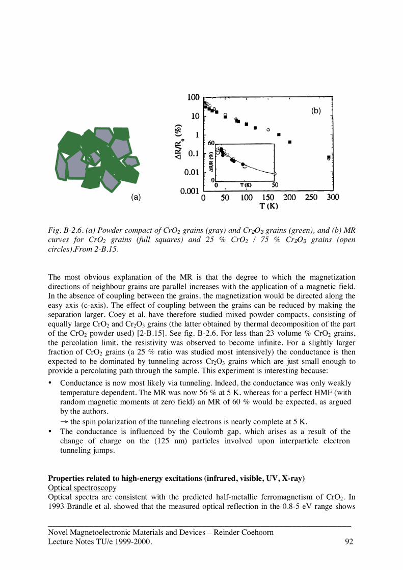
___________________________________________________________________Novel Magnetoelectronic Materials and Devices – Reinder CoehoornLecture Notes TU/e 1999-2000. 92
Fig. B-2.6. (a) Powder compact of CrO2 grains (gray) and Cr2O3 grains (green), and (b) MRcurves for CrO2 grains (full squares) and 25 % CrO2 / 75 % Cr2O3 grains (opencircles).From 2-B.15.
The most obvious explanation of the MR is that the degree to which the magnetizationdirections of neighbour grains are parallel increases with the application of a magnetic field.In the absence of coupling between the grains, the magnetization would be directed along theeasy axis (c-axis). The effect of coupling between the grains can be reduced by making theseparation larger. Coey et al. have therefore studied mixed powder compacts, consisting ofequally large CrO2 and Cr2O3 grains (the latter obtained by thermal decomposition of the partof the CrO2 powder used) [2-B.15]. See fig. B-2.6. For less than 23 volume % CrO2 grains,the percolation limit, the resistivity was observed to become infinite. For a slightly largerfraction of CrO2 grains (a 25 % ratio was studied most intensively) the conductance is thenexpected to be dominated by tunneling across Cr2O3 grains which are just small enough toprovide a percolating path through the sample. This experiment is interesting because:• Conductance is now most likely via tunneling. lndeed, the conductance was only weakly
temperature dependent. The MR was now 56 % at 5 K, whereas for a perfect HMF (withrandom magnetic moments at zero field) an MR of 60 % would be expected, as arguedby the authors.→ the spin polarization of the tunneling electrons is nearly complete at 5 K.
• The conductance is influenced by the Coulomb gap, which arises as a result of thechange of charge on the (125 nm) particles involved upon interparticle electrontunneling jumps.
Properties related to high-energy excitations (infrared, visible, UV, X-ray)Optical spectroscopyOptical spectra are consistent with the predicted half-metallic ferromagnetism of CrO2. In1993 Brändle et al. showed that the measured optical reflection in the 0.8-5 eV range shows
(a)
(b)
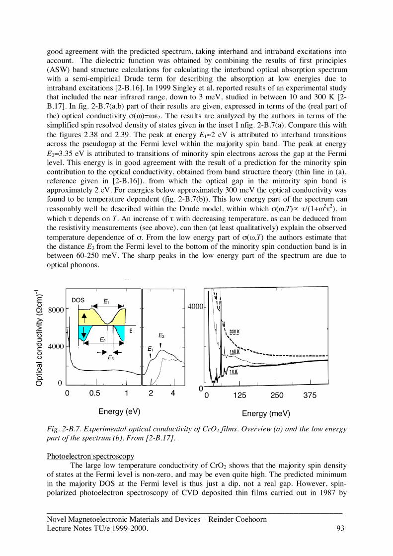
___________________________________________________________________Novel Magnetoelectronic Materials and Devices – Reinder CoehoornLecture Notes TU/e 1999-2000. 93
good agreement with the predicted spectrum, taking interband and intraband excitations intoaccount. The dielectric function was obtained by combining the results of first principles(ASW) band structure calculations for calculating the interband optical absorption spectrumwith a semi-empirical Drude term for describing the absorption at low energies due tointraband excitations [2-B.16]. In 1999 Singley et al. reported results of an experimental studythat included the near infrared range, down to 3 meV, studied in between 10 and 300 K [2-B.17]. In fig. 2-B.7(a,b) part of their results are given, expressed in terms of the (real part ofthe) optical conductivity σ(ω)=ωε2. The results are analyzed by the authors in terms of thesimplified spin resolved density of states given in the inset I nfig. 2-B.7(a). Compare this withthe figures 2.38 and 2.39. The peak at energy E1≈2 eV is attributed to interband transitionsacross the pseudogap at the Fermi level within the majority spin band. The peak at energyE2≈3.35 eV is attributed to transitions of minority spin electrons across the gap at the Fermilevel. This energy is in good agreement with the result of a prediction for the minority spincontribution to the optical conductivity, obtained from band structure theory (thin line in (a),reference given in [2-B.16]), from which the optical gap in the minority spin band isapproximately 2 eV. For energies below approximately 300 meV the optical conductivity wasfound to be temperature dependent (fig. 2-B.7(b)). This low energy part of the spectrum canreasonably well be described within the Drude model, within which σ(ω,T)∝ τ/(1+ω2τ2), inwhich τ depends on T. An increase of τ with decreasing temperature, as can be deduced fromthe resistivity measurements (see above), can then (at least qualitatively) explain the observedtemperature dependence of σ. From the low energy part of σ(ω,T) the authors estimate thatthe distance E3 from the Fermi level to the bottom of the minority spin conduction band is inbetween 60-250 meV. The sharp peaks in the low energy part of the spectrum are due tooptical phonons.
Fig. 2-B.7. Experimental optical conductivity of CrO2 films. Overview (a) and the low energypart of the spectrum (b). From [2-B.17].
Photoelectron spectroscopyThe large low temperature conductivity of CrO2 shows that the majority spin density
of states at the Fermi level is non-zero, and may be even quite high. The predicted minimumin the majority DOS at the Fermi level is thus just a dip, not a real gap. However, spin-polarized photoelectron spectroscopy of CVD deposited thin films carried out in 1987 by
0 0.5 1 2 4
Energy (eV)
0 125 250 375
Energy (meV)
4000
0
8000
4000
0Opt
ical
con
duct
ivity
(Ωcm
)-1
DOS
E
E1
E2
E3
E1
E2
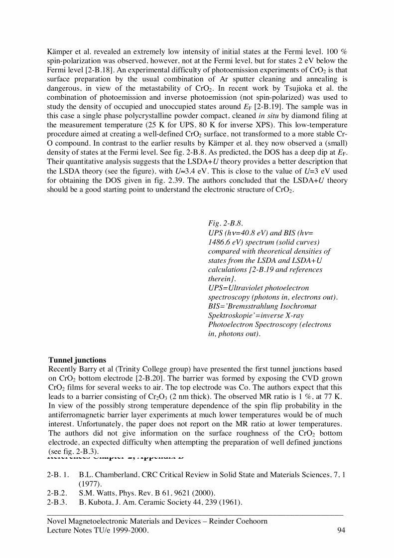
___________________________________________________________________Novel Magnetoelectronic Materials and Devices – Reinder CoehoornLecture Notes TU/e 1999-2000. 94
Kämper et al. revealed an extremely low intensity of initial states at the Fermi level. 100 %spin-polarization was observed, however, not at the Fermi level, but for states 2 eV below theFermi level [2-B.18]. An experimental difficulty of photoemission experiments of CrO2 is thatsurface preparation by the usual combination of Ar sputter cleaning and annealing isdangerous, in view of the metastability of CrO2. In recent work by Tsujioka et al. thecombination of photoemission and inverse photoemission (not spin-polarized) was used tostudy the density of occupied and unoccupied states around EF [2-B.19]. The sample was inthis case a single phase polycrystalline powder compact, cleaned in situ by diamond filing atthe measurement temperature (25 K for UPS, 80 K for inverse XPS). This low-temperatureprocedure aimed at creating a well-defined CrO2 surface, not transformed to a more stable Cr-O compound. In contrast to the earlier results by Kämper et al. they now observed a (small)density of states at the Fermi level. See fig. 2-B.8. As predicted, the DOS has a deep dip at EF.Their quantitative analysis suggests that the LSDA+U theory provides a better description thatthe LSDA theory (see the figure), with U≈3.4 eV. This is close to the value of U=3 eV usedfor obtaining the DOS given in fig. 2.39. The authors concluded that the LSDA+U theoryshould be a good starting point to understand the electronic structure of CrO2.
References Chapter 2, Appendix B
2-B. 1. B.L. Chamberland, CRC Critical Review in Solid State and Materials Sciences, 7, 1 (1977).
2-B.2. S.M. Watts, Phys. Rev. B 61, 9621 (2000).2-B.3. B. Kubota, J. Am. Ceramic Society 44, 239 (1961).
Fig. 2-B.8.UPS (hν=40.8 eV) and BIS (hν=1486.6 eV) spectrum (solid curves)compared with theoretical densities ofstates from the LSDA and LSDA+Ucalculations [2-B.19 and referencestherein].UPS=Ultraviolet photoelectronspectroscopy (photons in, electrons out).BIS=’Bremsstrahlung IsochromatSpektroskopie’=inverse X-rayPhotoelectron Spectroscopy (electronsin, photons out).
Tunnel junctionsRecently Barry et al (Trinity College group) have presented the first tunnel junctions basedon CrO2 bottom electrode [2-B.20]. The barrier was formed by exposing the CVD grownCrO2 films for several weeks to air. The top electrode was Co. The authors expect that thisleads to a barrier consisting of Cr2O3 (2 nm thick). The observed MR ratio is 1 %, at 77 K.In view of the possibly strong temperature dependence of the spin flip probability in theantiferromagnetic barrier layer experiments at much lower temperatures would be of muchinterest. Unfortunately, the paper does not report on the MR ratio at lower temperatures.The authors did not give information on the surface roughness of the CrO2 bottomelectrode, an expected difficulty when attempting the preparation of well defined junctions(see fig. 2-B.3).
___________________________________________________________________Novel Magnetoelectronic Materials and Devices – Reinder CoehoornLecture Notes TU/e 1999-2000. 95
2-B.4. R.C. DeVries, Mat. Res. Bull. 1, 83 (1966).2-B.S. L. Ranno, A. Barry and J.M.D. Coey, J. Appl. Phys. 81, 5774 (1997).2-B.6. R.J. Soulen, Jr. et al., Science 282, 85 (1998).2-B.7. K. Suzuki and P.M. Tedrow, Sol. State Comm. 107, 583 (1998).2-B.8. A. Gupta et al., Appi. Phys. Lett. 75, 2996 (1999).2-B.9. H.Y. Hwang and S.-W. Cheong, Science 278, 1607 (1997).2-B.10. K. Attenkofer and G. Schütz, J. de Physique IV, 7, Colloque C2, 459 (1997).2-B.11. A. Barry et al., J. Appl. Phys. 83, 7166 (1998).2-B.12. S.P. Lewis et al., Phys. Rev. B 55, 10253 (1997).2-B.13. X.W. Li et al., J. Appl. Phys. 85, 5585 (1999).2-B.14. K. Suzuki and P.M. Tedrow, Phys. Rev. B 58, 11597 (1998).2-B.15. J.M.D. Coey et al., Phys. Rev.Lett. 80, 3815 (1998).2-B.16 H. Brändle et al., Int. J. Mod. Phys. B7, 345 (1993).2-B.17 E.J. Singley et al., Phys. Rev. B 60, 4126 (1999).2-B.18 K.P. Kämper et al., Phys. Rev. B 59, 2788 (1987).2-B.19 T. Tsujioka et al., Phys. Rev. B 56, R15509 (1997).2-B.20 A. Barry et al., J. Phys. Cond. Matt. 12, L173 (2000).
___________________________________________________________________Novel Magnetoelectronic Materials and Devices – Reinder CoehoornLecture Notes TU/e 1999-2000. 96
References Chapter 2
2.1. See also the introductions to this subject in text books on solid state physics• C. Kittel, Introduction to Solid State Physics, 7th ed., Wiley, New York (1996),• N.W. Ashcroft and N.D. Mermin, Solid State Physics, Holt, Rinehart and Winston,
New York, (1976).• H. Ibach and H. Lüth, Solid State Physics, Springer, Berlin (1991).More advanced texts are• F. Gautier, “Itinerant magnetism”, in Magnetism of Metals and Alloys, ed. M.
Cyrot, North-Holland, Amsterdam (1982),• H. Capellmann (ed.), Metallic Magnetism, Springer, Berlin (1987).• V.A. Gubanov, A.I. Liechtenstein and A.V. Postnikov, Magnetism and the
electronic structure of crystals, Springer, Berlin (1992). Recommended!2.2. Parts of the text of sections 2.1-2.2 are based on R. Coehoorn, “Electronic structure
calculations for rare earth-transition metal compounds”, in Supermagnets, hardmagnetic materials, Ch. 8, p. 133-170, Kluwer, Dordrecht (1991).
2.3. P. Hohenberg and W. Kohn, Phys. Rev. 136, B864 (1964); W. Kohn and L.J. Sham,Phys. Rev. 140, A1133 (1965).
2.4. O.K. Andersen, Phys. Rev. B 12, 3060 (1975).2.5. H.L. Skriver, The LMTO Method, Springer, Berlin (1984)2.6. A.R. Williams, J. Kübler and C.D. Gelatt Jr., Phys. Rev. B 19, 6094 (1978).2.7. J.P. Perdew, J.A. Chevary, S.H. Vosko, K.A. Jackson, M.A. Pederson, D.J. Sing and
C. Fiolhais, Phys. Rev. B 46, 6671 (1992).2.8. V.L. Moruzzi, J.F. Janak and A.R. Williams, Calculated electronic properties of
metals, Pergamon, New York (1978).2.9. M. Asato, A. Settels, T. Hoshino, T. Asada, S. Blügel, R. Zeller and P.H. Dederichs,
Phys. Rev. B 60, 5202 (1999).2.10. H.J.F. Jansen, The electronic structure of iron, Ph.D. Thesis, Groningen (1981).2.11. R. Coehoorn, J. Magn. Magn. Mat. 159, 55 (1996).2.12. J. Hubbard, Proc. Roy. Soc. A 276, 238 (1963).2.13. P. Fulde, Y. Kakehashi abd G. Stollhoff, in Metallic Magnetism, p. 159, H.
Capellmann (ed.), Springer, Berlin (1987).2.14. B.I. Min, H.J.F. Jansen, T. Oguchi and A.J. Freeman, J. Magn. Magn. Mat. 61, 139
(1986).2.15. B.N. Cox, M. Coulthardt and P. Lloyd, J. Phys. F 4, 807 (1974).2.16. J.F. Herbst, R.E. Watson and J.W. Wilkens, Phys. Rev. B 31, 7603 (1985).2.17. R. Coehoorn, unpublished.2.18. The excitated hole states of Ni metal cannot be described completely in terms of the
calculated band structure below the Fermi energy. Photoelectron spectra show bands,but also excitations which can only be explained within a localized model withinwhich the ground state is regarded as a superposition of only a limited number ofatomic configurations, (mainly) 3d9 and 3d10.
2.19. E.C. Stoner, Proc. Roy. Soc. A 154, 656 (1936); E.C. Stoner, Proc. Roy. Soc. 165, 372(1938).
2.20. O. Gunnarsson, J. Phys. F 6, 587 (1976).2.21. The definition of the Stoner parameter used here leads to values of Ixc that are a factor
2 larger than the values given in [2.8].2.22. V.L. Moruzzi, P.M. Marcus and K. Schwarz, Phys. Rev. B 37, 790 (1986).2.23. S.C. Abrahams, L. Guttman and J.S. Kaspar, Phys. Rev. 127, 2052 (1962).
___________________________________________________________________Novel Magnetoelectronic Materials and Devices – Reinder CoehoornLecture Notes TU/e 1999-2000. 97
2.24. S. Mitani, A. Kida and M. Matsui, J. Magn. Magn. Mat. 126, 76 (1993).2.25. R.A. de Groot, D.D. Koelling and F.M. Mueller, J. Phys. F 10, L235 (1980).2.26. E.P. Wohlfarth, in Ferromagnetic Materials, vol. 1, E.P. Wohlfarth (ed.), North-
Holland, Amsterdam, pp 26-28 (1980).2.27. M. Shimizu, Rep. Progr. Phys. 44, 21 (1981).2.28. T. Moriya, in Spin fluctations in Itinerant Electron Magnetism, Springer, Berlin
(1985).2.29. J. Kübler, A.R. Williams and C.B. Sommers, Phys. Reb. B28, 1745 (1983).2.30. N. Metropolis et al., The J. of Chem. Phys. 21, 1087 (1953) (about the Monte Carlo
method); D.S. Richie and M.E. Fisher, Phys. Rev. 5, 2668 (1972); M. Ferer andA.Hamid-Aidinejad, Phys. Rev. B34, 6481 (1986); K. Chen et al., Phys. Rev. B48,3249 (1993).
2.31. M.V. You, V. Heine, A.J. Holden and P.J. Lin-Chung, Phys. Rev. Lett. 44, 1282(1980).
2.32. V. Heine, J.H. Samson and C.M.M. Nex, J. Phys. F. 11, 2645 (1981).2.33. M.V. You and V. Heine, J. Phys. F 12, 177 (1982).2.34. A.J. Holden and M.V. You, J. Phys. F 12, 195 (1982).2.35. A.J. Holden, V. Heine and J.H. Samson, J. Phys. F 14, 1005 (1984).2.36. L.M. Small and V. Heine, J. Phys. F. 14, 3041 (1984).2.37. E.M. Haines, V. Heine and A. Ziegler, J. Phys. F 16, 1343 (1986).2.38. M.U. Luchini and V. Heine, J. Phys.: Cond. Matter 1, 8961 (1989).2.39. K.S. Chana, J.H. Samson, M.U. Luchini and V. Heine, J. Phys.: Cond. Matter 3, 6455
(1991).2.40. M.U. Luchini, V. Heine and G.J. McMullan, J. Phys.: Cond. Matter 3, 8647 (1991).2.41. M.U. Luchini and V. Heine, Europhys. Lett. 14, 609 (1991).2.42. K.S. Chana, J.H. Samson, M.U. Luchini and V. Heine, J. Magn. Magn. Mat. 104-107,
743 (1992).2.43. A.J. Lichtenstein, M.I. Katsnelson, V.P. Antropov and V.A. Gubanov, J. Magn. Magn.
Mat. 67, 65 (1987).2.44. R.F. Sabirov, S.K. Bose and O.N. Mryasov, Phys. Rev. B 51, 8958 (1995).2.45. R.F. Sabiryanov and S.S, Jaswal, Phys. Rev. Lett. 79, 155 (1997).2.46. R.F. Sabiryanov and S.S. Jaswal, Phys. Rev. B 57, 7767 (1998).2.47. R.F. Sabiryanov and S.S. Jaswal, Phys. Rev. Lett. 83, 2062 (1999).2.48. V.P. Antropov, B.N. Harmon and A.N. Smirnov, J. Magn. Magn. Mat. 200, 148
(1999).2.49. M. Uhl and J. Kübler, Phys. Rev. Lett. 77, 334 (1996).2.50. L.M. Sandratskii, Adv. in Phys. 47, 91 (1998).2.51. T. Moriya, “Electron correlation and Magnetism in Narrow-band systems”, Springer
Series in Solid State Sciences 29, Springer, Berlin (1981).2.52. M. Shimizu, Rep. Progr. Phys. 44, 330-409 (1981).2.53. P.D. Johnson, Rep. Progr. Phys. 60, 1217-1304 (1997).2.54. R.A. de Groot, F.M. Mueller, P.G. van Engen and K.H.J. Buschow, Phys. Rev. Lett.
50, 2024 (1983).2.55. P.G. van Engen, K.H.J. Buschow and R. Jongebreur, Appl. Phys. Lett. 42, 202 (1983).2.56. R.A. de Groot and K.H.J. Buschow, J. Magn. Magn. Mat. 54-57, 1377 (1986).2.57. R.A. de Groot, F.M. Mueller, P.G. van Engen and K.H.J. Buschow, J. Appl. Phys. 55,
2151 (1984).2.58. R.B. Helmholdt, R.A. de Groot, F.M. Mueller, P.G. van Engen and K.H.J. Buschow,
J. Magn. Magn. Mat. 43, 249 (1984).2.59. H. van Leuken and R.A. de Groot, Phys. Rev. Lett. 74, 1171 (1995).
___________________________________________________________________Novel Magnetoelectronic Materials and Devices – Reinder CoehoornLecture Notes TU/e 1999-2000. 98
2.60. J. Kuebler, Physica 127B (1984) 257.2.61. R.A. de Groot, A.M. van der Kraan and K.H.J. Buschow, J. Magn. Magn. Mat. 61,
330 (1986).2.62. R.A. de Groot, Physica B 172, 45 (1991).2.63. D. Orgassa, H. Fujiwara, T.C. Schulthess and W.H. Butler, Phys. Rev. B 60, 13237
(1999).2.64. R. Coehoorn, unpiblished (2000).2.65. S.J. Youn and B.I. Min, Phys. Rev. B. 51, 10436 (1995).2.66. I. Galanakis et al., Phys. Rev. B. 61, 4093 (2000).2.67. X. Wang et al., IEEE Trans. MAG. 30, 4458 (1994).2.68. J. Pierre et al., J. Alloys and Compounds 262-263, 101 (1997); J. Tobola and J. Pierre,
J. Alloys and Compounds 296, 243 (2000).2.69. S. Ishida et al., J. Phys. Cond. Matt. 8, 6889 (1996).2.70. R.C. Albers et al, Phys. Rev. 36, 3661 (1987).2.71. S. Ishida et al., J. Phys. Soc. Japan, 64, 2152 (1995).2.72. S. Ishida et al., Physica B 245, 1 (1998); Physica B 254, 157 (1998).2.73. S. Fujii et al., J. Phys. Soc. Japan 63, 1881 (1994);2.74. S. Fujii et al., J. Phys. Soc. Japan 64, 185 (1995).2.75. S. Ishida et al., Physica B 210, 140 (1995); J. Phys. Cond. Mat. 8, 6889 (1996).2.76. P.J. Brown et al., J. Phys. Cond. Matter 12, 1827 (2000).2.77. K. Schwarz, J. Phys. F: Met. Phys. 16, L211-L215 (1986).2.78. M.A. Korotin, V.I. Anisimov, D.I. Khomskii and G.A. Sawatzky, Phys. Rev. Lett. 80,
4305 (1998).2.79. V.I. Anisimov et al., Phys. Rev. B 44, 943 (1991); A.I. Lichtenstein et al., Phys. Rev.
B 52, R5467 (1995); W.E. Pickett et al., Phys. Rev. B 58, 1201 (1998).2.80. N.F. Mott, Metal-insulator transitions, Taylor & Francis Ltd, London (1974).2.81. C. Zener, Phys. Rev. 82, 403 (1951).2.82. P.W. Anderson and H. Hasegawa, Phys. Rev. 100, 675 (1955).2.83. H. van Leuken and R.A. de Groot, Phys. Rev. B 51, 7176 (1995).
Added in 2001 (overview article):W.E. Picket and J.S. Moodera, "Half metallic Magnets", Physics Today 54, 39 (2001).