novel intelligent power supply using a modified pulse
TRANSCRIPT

Wright State University Wright State University
CORE Scholar CORE Scholar
Browse all Theses and Dissertations Theses and Dissertations
2009
Novel Intelligent Power Supply using a Modified Pulse Width Novel Intelligent Power Supply using a Modified Pulse Width
Modulator Modulator
Gary Richard Doss Jr. Wright State University
Follow this and additional works at: https://corescholar.libraries.wright.edu/etd_all
Part of the Electrical and Computer Engineering Commons
Repository Citation Repository Citation Doss, Gary Richard Jr., "Novel Intelligent Power Supply using a Modified Pulse Width Modulator" (2009). Browse all Theses and Dissertations. 313. https://corescholar.libraries.wright.edu/etd_all/313
This Thesis is brought to you for free and open access by the Theses and Dissertations at CORE Scholar. It has been accepted for inclusion in Browse all Theses and Dissertations by an authorized administrator of CORE Scholar. For more information, please contact [email protected].

Novel Intelligent Power Supply Using a Modified
Pulse Width Modulator
A thesis submitted in partial fulfillment
of the requirements for the degree of
Master of Science in Engineering
By
GARY RICHARD DOSS, JR.,
B.S., Wright State University, 2004
2009
Wright State University

WRIGHT STATE UNIVERSITY
SCHOOL OF GRADUATE STUDIES
August 14, 2009
I HEREBY RECOMMEND THAT THE THESIS PREPARED UNDER MY
SUPERVISION BY GARY RICHARD DOSS, JR., ENTITLED NOVEL
INTELLIGENT POWER SUPPLY USING A MODIFIED PULSE WIDTH
MODULATOR BE ACCEPTED IN PARTIAL FULFILLMENT OF THE
REQUIREMENTS FOR THE DEGREE OF MASTER OF SCIENCE IN
ENGINEERING.
____________________________
Marian K. Kazimierczuk, Ph.D. Thesis Director
____________________________
Kefu Xue, Ph.D.
Department Chair
Committee on Final Examination ____________________________
____________________________
Marian K. Kazimierczuk, Ph.D. Xiaodong Zhang, Ph.D. ____________________________
____________________________
Kuldip S. Rattan, Ph.D. ____________________________
Joseph F. Thomas, Jr., Ph.D. Dean, School of Graduate Studies

iii
Abstract
Doss Jr., Gary Richard. M.S.E., Department of Electrical Engineering, Wright
State University, 2004. Novel Intelligent Power Supply Using a Modified Pulse
Modulator
The objective of this M.S. Thesis was to design, simulate, construct and test a
pulse-width-modulated Buck DC-DC Converter and its compensated feedback
system. Equations for the design and component selection of a buck converter
have been obtained for operating the buck converter in the continuous
conduction mode (CCM). A hardware version of the converter design has been
implemented to demonstrate the functionality of the designed converter. Also, a
digital buck converter control system has been designed and simulated. This
digital buck converter led to the development of a proposed control scheme for
Switched Mode Power Supplies (SMPS).
A novel hybrid feedback control scheme has been proposed, analyzed and
simulated. This proposed novel control system implements a proposed novel
device that accepts commands from an intelligent source, such as a processor,
while allowing the SMPS to apply power to the system under analog control.
Once the processor is functioning, it can adjust and tweak characteristics of the
power supply to obtain the best power output for the operating environment.

iv
Table of Contents
Abstract ................................................................................................................iii
Table of Contents .................................................................................................iv
List of Figures......................................................................................................vii
Dedication .......................................................................................................... xiii
Chapter 1 Introduction .......................................................................................... 1
Chapter 2 Buck DC-DC Converter........................................................................ 2
2.1 Analog Switch Mode Power Supply Design ................................................ 4
2.2 Cross Conduction ....................................................................................... 7
Chapter 3 Design of a Buck Converter ............................................................... 11
Chapter 4 Capacitor Selection............................................................................ 16
4.1 Equivalent Series Resistance ................................................................... 16
4.2 Capacitor Ripple Current........................................................................... 18
4.3 Wet Electrolytic Capacitors ....................................................................... 20
4.4 Ceramic Capacitor .................................................................................... 21
4.5 Solid Electrolytic Capacitors...................................................................... 23

v
4.6 Selection ................................................................................................... 23
Chapter 5 Inductor.............................................................................................. 25
5.1 Air-Core Design ........................................................................................ 30
5.2 Iron Ferrite Design .................................................................................... 33
5.3 Inductor Construction................................................................................ 37
Chapter 6 Analog Simulation.............................................................................. 38
6.1 Output Stage Simulation Design ............................................................... 38
6.2 PWM Design ............................................................................................. 41
6.4 Open Loop Transfer Functions ................................................................. 42
6.5 Closed loop ............................................................................................... 52
6.6 Buck Design Implementation .................................................................... 69
Chapter 7 Digital Switch Mode Power Supply Design ........................................ 79
Chapter 8 Modified Switch Mode Power Supply Design..................................... 86
Chapter 9 Conclusion ......................................................................................... 96
Appendix A SG1526 PWM Datasheet ................................................................ 98
Appendix B DSCC MIL-PRF-39006/22H, Table I ............................................. 107

vi
Appendix C DSCC MIL-PRF-39014/22E Table III ............................................ 114
Appendix D DSCC MIL-PRF-39003/10C CSS13 Table I.................................. 119
References ....................................................................................................... 123
vii
List of Figures
Figure Page
Figure 2.1 A simplified diagram of a buck DC-DC converter and its general
operating waveforms. ........................................................................................... 3
Figure 2.2 A simplified functional diagram of a conventional PWM. .................... 4
Figure 2.3 The analog pulse width production scheme. ...................................... 5
Figure 2.4 A simplified functional analog synchronous buck DC-DC converter. .. 6
Figure 2.5 A typical adaptive gate drive from [4].................................................. 9
Figure 2.6 An example of transistor Q2 being turned on when transistor Q1 is
turn on, [4]. ......................................................................................................... 10
Figure 4.1 Example capacitor model with Equivalent Series Resistance. ......... 18
Figure 4.2 Example construction of an Electrolytic Capacitor............................ 21
Figure 4.3 Ceramic capacitor construction showing interlacing finger plates. ... 22
Figure 5.1 Uniform field lines from a tightly wound solenoid inductor. ............... 26
viii
Figure 5.2 A solenoid inductor showing magnetic field lines. ............................ 27
Figure 5.3 Hysteresis of Magnetics Inc. E-Core 45528. .................................... 33
Figure 6.1 Buck converter model showing resistive elements of the inductor and
capacitor. ............................................................................................................ 39
Figure 6.2 Simulink model of the buck converter output stage. ......................... 41
Figure 6.3 The Simulink model of a simple PWM.............................................. 42
Figure 6.4 Small signal model of a buck converter [1]. ...................................... 43
Figure 6.5 Output stage of the buck converter................................................... 43
Figure 6.6 Impedance equivalent of the output stage shown in Figure 6.5........ 44
Figure 6.7 Open loop block diagram of the buck converter. .............................. 48
Figure 6.8 Bode diagram of the buck converter of transfer function, TP, without
compensation. .................................................................................................... 49

ix
Figure 6.9 Open loop step response of the plant transfer function, TP. .............. 50
Figure 6.10 Simulink model of a buck converter with no feedback. ................... 51
Figure 6.11 Plot of buck converter voltage and current output with changing
load..................................................................................................................... 52
Figure 6.12 Open loop step response of TK....................................................... 54
Figure 6.13 Bode plot of TK. .............................................................................. 54
Figure 6.14 PI control circuit. ............................................................................. 55
Figure 6.15 Bode plot of TC. .............................................................................. 58
Figure 6.16 Bode plot of T. ................................................................................ 59
Figure 6.17 Nyquist diagram of T confirms the Phase Margin in Figure 6.16. ... 59
Figure 6.18 Step response of TCL. ..................................................................... 61
Figure 6.19 Bode diagram of Tcl. ...................................................................... 61

x
Figure 6.20 Closed loop block diagram of the buck converter. .......................... 63
Figure 6.21 Buck converter with feedback......................................................... 63
Figure 6.22 Plot of the buck converter voltage output with feedback while the
load varies. ......................................................................................................... 64
Figure 6.23 Scaled plot in Figure 6.15 overlaid on the output of the buck
converter model.................................................................................................. 65
Figure 6.24 Ripple voltage of the buck output voltage....................................... 65
Figure 6.25 A bode plot of the closed loop audio susceptibility. ........................ 67
Figure 6.26 Audio susceptibility due to a unit step disturbance on the input
voltage. ............................................................................................................... 68
Figure 6.27 Unit step response disturbance on the input voltage of the buck
model.................................................................................................................. 69
Figure 6.28 A schematic of the simple buck converter. ..................................... 70

xi
Figure 6.29 Recorded signals from the simple buck converter. Channel 1 is the
ramp signal, channel 2 is the feedback signal, channel 3 is the switching signal,
and channel 4 is the output of the buck converter. ............................................. 72
Figure 6.30 A schematic of the synchronous buck converter. ........................... 74
Figure 6.31 Recorded signals from the synchronous buck converter. Channel 1
is the feedback voltage, channel 2 is the ramp signal, channel 3 is the switching
signal, and channel 4 is the output voltage......................................................... 76
Figure 6.32 The steady state response of the load impedance being switched
from 4.1 Ω to 1 Ω................................................................................................ 78
Figure 7.1 A simplified functional diagram of a digital buck DC-DC converter... 80
Figure 7.2 A Simulink model of the buck converter with Digital feedback control.
........................................................................................................................... 83
Figure 7.3 A output voltage and current plot of the digital buck converter with a
varying load. ....................................................................................................... 84
Figure 8.1 A SMPS with analog control at start-up using MPWM...................... 87
xii
Figure 8.2 The CPU is out of reset and able to adjust aspects of the buck
converter. ........................................................................................................... 87
Figure 8.3 A Function diagram of the Modified Pulse Width Modulator. ............ 89
Figure 8.4 Simulink model of Modified Pulse Width Modulator........................... 90
Figure 8.5 The buck model with a simulated CPU in an outer control loop. ...... 91
Figure 8.6 Analog control loop gain changed from 0.5 to 0.45. .......................... 93
Figure 8.7 The ripple amplitude and DC output changed by the CPU. ............... 94

xiii
Dedication
To my wife, whose love and support have made everything possible.

1
Chapter 1 Introduction
In recent years new developments in Switched Mode Power Supply (SMPS)
designs have incorporated microcontrollers. These microcontrollers are replacing
analog components within a classic SMPS to produce the required pulse width
modulated signal. The advantages of using a microcontroller are the ability to
enact advanced control schemes, robust operation, and user interaction. The
largest disadvantage of using a microcontroller is lower power efficiency.
By replacing the Pulse Width Modulator (PWM) in an SMPS with a component
that can enact commands from an intelligent source but not contain the power
hungry components found in microcontrollers, such as memory, a power supply
can gain the benefits of intelligent control and the benefits of a power efficient
design by allowing the Central Processing Unit (CPU) in the computer system to
receive feedback information from the power supply and make decisions on any
needed adjustments within the power supply. At power on or start-up of the CPU
this modified PWM regulates the output of the power supply based on an analog
control scheme. After the CPU is started it begins making adjustments to the
power supply to obtain the most efficient and effective output.

2
Chapter 2 Buck DC-DC Converter
This thesis will use a simple Buck DC-DC Converter for analysis. A ‘buck
converter’ is a Switched Mode Power Supply (SMPS) that converts a DC voltage
input to a lower DC voltage more efficiently than a resistive voltage divider or
linear power supply. A simple buck converter uses two switches (a transistor and
diode), an inductor, and a capacitor. When the transistor is closed the capacitor
and inductor are charged. When the transistor opens the energy stored in the
inductor and capacitor is discharged through the load. The output voltage of a
buck SMPS can be calculated using equations from [1] and [2] by:
DVV IO ×= (2.1)
where
IV , input DC voltage to the Buck DC-DC Converter
OV , output DC voltage of the Buck DC-DC Converter
D , percentage the switching signal is high with respect to the period
Figure 2.1 shows a simplified functional schematic and waveforms of a buck
converter. When switch Q is closed inductor L and capacitor C are charged and
provide power to the load; illustrated in the diagram. When switch Q is opened
the diode D begins conducting current and the inductor L and capacitor C
discharge through the load. The graph to the right of the circuit diagrams shows

3
the voltage and current response as the ‘Switch State’ of the transistor Q
transitions from on to off.
Figure 2.1 A simplified diagram of a buck DC-DC converter and its general operating
waveforms.
Due to the switching of the transistor Q the output current and voltage of the buck
converter will ripple about the intended DC voltage output of the buck converter.
Too much ripple voltage may cause components to malfunction. The ripple
voltage is due to the charging and discharging of the capacitor C and can be
described by the following equation from [1]:
fL
DVr
LCf
DVV MINOCMINO )1(
8
)1(2
−+
−=∆ (2.2)
4
where
V∆ , ripple voltage output of the buck converter
OV , output DC voltage of the buck converter
f , frequency of the PWM signal
L , inductor value in Henry
C , capacitor value in Farad
Cr , Equivalent Series Resistance of the capacitor
MIND , minimum duty cycle
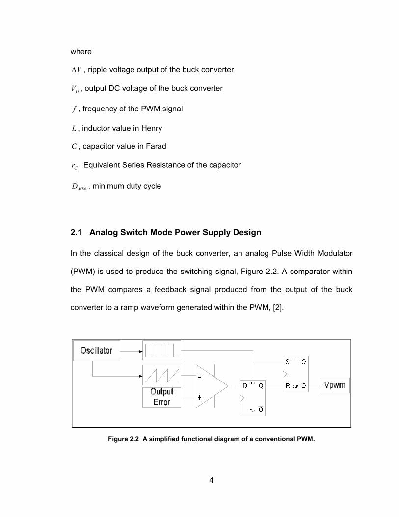
2.1 Analog Switch Mode Power Supply Design
In the classical design of the buck converter, an analog Pulse Width Modulator
(PWM) is used to produce the switching signal, Figure 2.2. A comparator within
the PWM compares a feedback signal produced from the output of the buck
converter to a ramp waveform generated within the PWM, [2].
Figure 2.2 A simplified functional diagram of a conventional PWM.

5
Figure 2.3 The analog pulse width production scheme.
As illustrated in Figure 2.2, as the output voltage of the buck converter, functional
diagram shown in Figure 2.3, becomes lower the pulse width of the switching
signal becomes wider. In Equation 2.1, the wider the pulse width (or duty cycle)
of the switching signal the larger the output voltage of the buck converter. Figure
2.4 shows a buck converter with the above analog PWM incorporated with
feedback. In Figure 2.4, the diode in the previous buck converter illustration has
been replaced with transistor, Q2, making a synchronous buck converter.
Vref
Vref
Vpwm
Vpwm
6
Output
Error
-
+Q
QSET
CLR
D
Oscillator
Supply C
L
LOAD
Q1
Q2
Driver
Conventional Analog PWM
Voltage
Reference
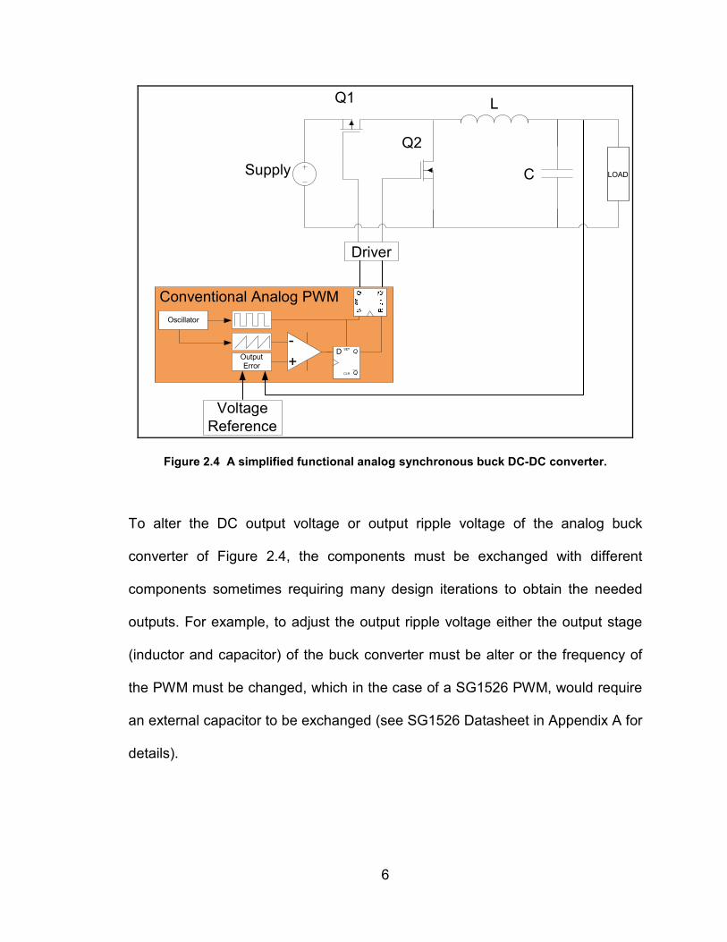
Figure 2.4 A simplified functional analog synchronous buck DC-DC converter.
To alter the DC output voltage or output ripple voltage of the analog buck
converter of Figure 2.4, the components must be exchanged with different
components sometimes requiring many design iterations to obtain the needed
outputs. For example, to adjust the output ripple voltage either the output stage
(inductor and capacitor) of the buck converter must be alter or the frequency of
the PWM must be changed, which in the case of a SG1526 PWM, would require
an external capacitor to be exchanged (see SG1526 Datasheet in Appendix A for
details).
7
The components in an analog SMPS must be de-soldered in order to alter the
SMPS after the design is implemented. This makes obtaining a precise DC
output and desired output voltage ripple more difficult, especially if the device is
fielded.
The DC output and ripple voltage can alter over time due to component values
and properties changing because of ageing and other factors, such as the
environment in which the system is used. The poor performance in a system’s
power supply can result in a domino effect of poor performance of the
downstream components that are depending on a stable, reliable source of
power for correct operation and performance. To correct this, again, would
require exchanging components to make corrections for these changes.
2.2 Cross Conduction
The buck converter circuit configuration shown in Figure 2.4 is commonly known
as a synchronous buck converter. A synchronous buck converter is a buck
converter whose diode (shown in the simple buck converter in Figure 2.1 above)
is replaced with another transistor as seen in Figure 2.4. Using this transistor in
place of a diode allows for better control of the buck converter and better
efficiency ratings with little or no impact to the buck converter’s footprint. A
problem with this configuration is it can suffer from an effect known as cross-
conduction or shoot-through ([1], [3]).

8
Cross-conduction, or shoot-through, is the condition when both transistor Q1 and
transistor Q2 are turned on at the same time or when transistor Q2 is in the
process of turning off when transistor Q1 is turned on or is in the process of
turning on. This allows the current to momentarily ‘shoot-through’ from the power
supply to ground. This condition can result in lower overall efficiency of the buck
converter and limit the life of the transistors due to high current and overheating.
To control or limit cross conduction, a buck converter design can use one of two
methods ([4]).
The first method is to create a fixed delay in switching between transistor Q1 and
transistor Q2. This can be done in a digital buck converter, where switching is
controlled by a microcontroller, through software by inserting a delay in the
command to turn off transistor Q1 and turn on transistor Q2. However, in an
analog buck converter a delay can be inserted by adding a delay circuit.
The second method is to create an adaptive gate delay. Again, this can be
implemented in the software of a digital buck converter; otherwise a circuit will
need to be added to the buck converter design that adjusts the delay time
according the load conditions. An example adaptive delay circuit can be seen in
Figure 2.5 from [4].

9
Figure 2.5 A typical adaptive gate drive from [4].
The disadvantage to adding a delay is it can decrease the available pulse width
or duty cycle resulting in less command authority to drive the output of the buck
converter to the proper output voltage under heavy load conditions. Also, a delay
is not a guaranteed solution to prevent cross conduction.
Cross conduction can also occur when the transition rate from off-to-on of
transistor Q1 is too high. When transistor Q1 is turned on at a high rate, dV/dt,

10
while transistor Q2 is off, the sudden transition on the drain of transistor Q2 can
cause it to be turned on momentarily due to parasitic capacitances and
inductances as illustrated in the following Figure from [4].
Figure 2.6 An example of transistor Q2 being turned on when transistor Q1 is turn on, [4].

11
Chapter 3 Design of a Buck Converter
The design of the buck converter will need to satisfy the requirements needed for
the system. The input supply voltage will be from a 12 V DC source with a
maximum variance of ±2 V. The output voltage of the buck converter will need to
supply the system with 5 V whose error can be no more than ±0.25 V (or a 5%
error) after turn on and when the output is at steady-state. The current can vary
from 1.25 AMIN to 25 AMAX.
The ripple voltage is the amount of oscillation on the output of the buck
converter. This oscillation is caused by switching within the buck converter
caused by the Pulse Width Modulator (PWM) and can be limited by the output
capacitance and the capacitor’s Equivalent Series Resistance (ESR). Too much
voltage ripple on the power supply to system components may cause the
components to malfunction. Too little ripple voltage may require many capacitors
in a system that has limited space for components or dramatically increase the
cost of the system. For the purposes of this thesis the buck converter must have
a ripple voltage less than or equal to 0.25 VPP.
The output power of the system will be determined using the maximum and
minimum current of the system as described above by first calculating the
maximum and minimum load resistance output requirement of the system.

12
Ω==
Ω====
4
2.0
OMin
OMax
OMax
OMin
O
O
I
VR
I
VR
I
VR
(3.1)
==
====
W125
W25.6
OMaxOOMax
OMinOOMin
OOO
IVP
IVP
IVP (3.2)
Using the input and output voltage requirements for the buck converter, the
transfer function can be calculated for use in determining the PWM duty cycle, D.
From the equation )( IOVDC VVMD ηη == found on page 46 of [1], the maximum,
minimum and nominal transfer function (MVDC) values are;
35.0V14
V5===
IMax
OVDCMin
V
VM (3.3)
42.0V12
V5===
INom
OVDCNom
V
VM (3.4)
5.0V10
V5===
IMin
OVDCMax
V
VM (3.5)

13
The duty cycle for each of the three transfer functions above can now be
calculated assuming the efficiency of the buck converter (η ) is 85%;
412.085.0
35.0===
ηVDCMin
Min
MD (3.6)
49.085.0
41.0===
ηVDCNom
Nom
MD (3.7)
59.085.0
5.0===
ηVDCMax
Max
MD (3.8)
Assuming the switching frequency of the PWM is 100 kHz, the value of the
inductor can be calculated to be;
( )fL
DVDT
L
VVDT
L
Vt
L
Vi
t
iLV OOILL
LL
L
−=
−==∆=∆→
∆∆
=1
(3.9)
( )fL
DViI OLO
2
1
2
−=
∆= (3.10)
( )DfL
I
VR
O
O
−==
1
2 (3.11)

14
( ) ( ) ( )µH8.11
1000002
41.014
2
1
2
1=
×−
=−
=−
=f
DR
f
DRL MinMax
(3.12)
where
LV , voltage across the inductor
IV , input DC voltage to the buck DC-DC converter
OV , output DC voltage of the buck DC-DC converter
f , frequency of the PWM signal
L , inductor value in Henry
C , capacitor value in Farad
D , duty cycle
The output capacitor holds up the output voltage of the buck converter during
switching of transistors Q1 and Q2. The capacitor’s ESR controls the magnitude
of the output ripple voltage being the dominant component in the second term in
Equation 2.2. Using Equation 2.58 from [1] a minimum capacitor value can be
calculated assuming the inductor is 15 µH. The capacitor value is calculated by
determining the maximum ripple current through the inductor ( LMAXi∆ ) and
maximum ESR (rC) by:
A97.11015100000
)41.01(5)1(6=
××−
=−
=∆ −fL
DVi MINOLMAX (3.13)

15
Ω127.097.1
25.0==
∆=
LMAX
rCMAX
i
Vr (3.14)
Let rC equal 0.13 Ω.
µF6.2413.01015100000
412.01,59.0max
2
1,max,max
6
)()(
=×××
−=
−==
−
C
MinMAX
offMAXonMINMinfr
DDCCC
(3.15)
where
rV , ripple voltage
LMAXi∆ , maximum ripple current through the inductor
Cr , maximum ESR allowed to be less than the maximum ripple voltage
f , frequency of the PWM signal
L , inductor value in Henry
C , capacitor value in Farad
D , duty cycle
From above, the buck converter design will have a 15 µH inductor and a 30 µF
capacitor who’s ESR is less than 0.13 Ω.

16
Chapter 4 Capacitor Selection
Capacitors vary not only in capacitance but also by type. Different types of
capacitors provide high capacitance but cannot tolerate large amounts of ripple
current. Whereas, others provide a high tolerance for ripple or AC current but do
not provide high capacitance. Therefore, careful consideration must be taken to
select the right capacitor that will not fail over time due to excessive stress and
provide sufficient output capacitance for the switched mode power supply.
4.1 Equivalent Series Resistance
Equivalent Series Resistance (ESR) is a modeled resistive element placed in
series with an ideal capacitor that accounts for the power lost in a real capacitor
due to imperfections in the capacitors materials. ESR can vary due to capacitor
type, temperature, and frequency of charging and discharging.
In switching mode power supplies (SMPS), ESR can be particularly important
due to the desired efficiency and life of the SMPS. The higher the ESR of the
output capacitor the greater the heat will be generated due to the continuous flow
of current across the ESR. The more heat generated by the capacitor lowers the
life expectancy of the capacitor and lowers the overall efficiency of the SMPS.

17
To determine the ESR of a capacitor, an empirical measurement can be made of
various capacitors using an LCR meter (Inductance, Capacitance and
Resistance meter). Because of the numerous different capacitors, an analytical
worse case calculation can be made to avoid the time consuming empirical
method.
Using the “Dissipation Factor” (DF) specified in a capacitors manufacturers
datasheet (Q Factor is sometimes found instead which is the inverse of the
Dissipation Factor) a calculation can be made that provides the general worse
case ESR of that particular capacitor. The Equation 4.1 can be used to calculate
the maximum ESR ( ESRMaxR ) of the capacitor with respect to the frequency of the
applied signal.
fC
DFRESRMax π2
= (4.1)
where
DF = maximum dissipation factor
f = frequency of applied signal
C = nominal capacitance
18
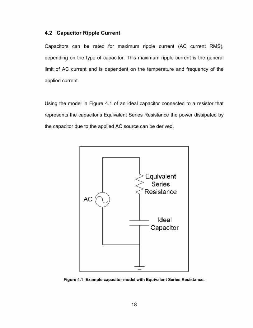
4.2 Capacitor Ripple Current
Capacitors can be rated for maximum ripple current (AC current RMS),
depending on the type of capacitor. This maximum ripple current is the general
limit of AC current and is dependent on the temperature and frequency of the
applied current.
Using the model in Figure 4.1 of an ideal capacitor connected to a resistor that
represents the capacitor’s Equivalent Series Resistance the power dissipated by
the capacitor due to the applied AC source can be derived.
Figure 4.1 Example capacitor model with Equivalent Series Resistance.
19
The power dissipated by the ESR, ESRR , can be determine using the power
equation, RVP 2= , as follows;
22
2222
))(707.0)(5.0(
CESR
ESRRMS
ESR
CESR
ESRPP
ESR
ESRRMSRMSRMS
ZR
RV
R
ZR
RV
R
VIVP
+=
+=== (4.2)
Using the power equation above, the root mean square (assuming a worse case
applied sinusoidal signal) current applied to a capacitor is given as;
PPESR
CESRRMS
CESR
ESRPP
RMS
RMS
RMSRMS
VR
ZRP
ZR
RV
P
V
PI
)2)(2(
)707.0)(5.0(
22
22
+=
+
== (4.3)
where
fCZC π2
1= , impedance of the ideal capacitor
PPV , is the voltage ripple peak to peak
Using this equation along with the maximum ESR, a worse case ripple current
can be calculated for the designed switched mode power supply. This current
calculation will allow a capacitor or group of capacitors to be selected that can
accommodate the specified output voltage ripple design specifications discussed

20
earlier and help ensure proper operation throughout the life of the switched mode
power supply.
4.3 Wet Electrolytic Capacitors
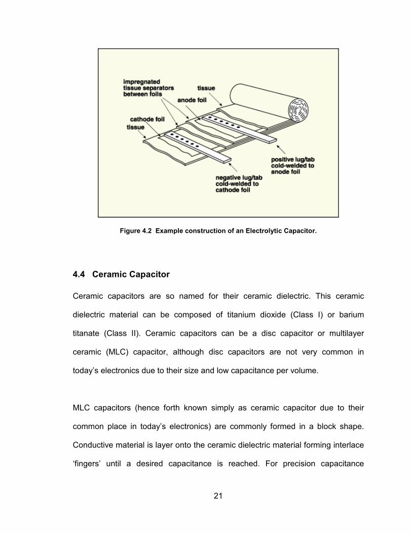
Wet electrolytic capacitors can be composed of aluminum or tantalum. Aluminum
wet electrolytic capacitors are generally made of two pieces of aluminum. One of
these pieces of aluminum is coated with a non-conductive aluminum oxide which
is the capacitor’s dielectric material. This aluminum foil coated in aluminum oxide
is the anode of the capacitor. A paper spacer soaked in wet electrolyte separates
the anode from the second aluminum foil or cathode. These two pieces of
aluminum with attached leads get rolled together with the electrolyte soaked
paper and a second paper spacer to form a wet aluminum electrolytic capacitor.
Wet electrolytic tantalum capacitors are formed in a similar manner as wet
aluminum electrolytic capacitors except the dielectric material is tantalum oxide.
Figure 4.2 below, from [5], shows an example construction of an aluminum
electrolytic capacitor.
21
Figure 4.2 Example construction of an Electrolytic Capacitor.
4.4 Ceramic Capacitor
Ceramic capacitors are so named for their ceramic dielectric. This ceramic
dielectric material can be composed of titanium dioxide (Class I) or barium
titanate (Class II). Ceramic capacitors can be a disc capacitor or multilayer
ceramic (MLC) capacitor, although disc capacitors are not very common in
today’s electronics due to their size and low capacitance per volume.
MLC capacitors (hence forth known simply as ceramic capacitor due to their
common place in today’s electronics) are commonly formed in a block shape.
Conductive material is layer onto the ceramic dielectric material forming interlace
‘fingers’ until a desired capacitance is reached. For precision capacitance

22
requirements, these capacitors can be etched or cut to achieve an exact
capacitance value. Figure 4.3 below shows an example construction illustrating
the interlaced ‘finger’ plates of a standard ceramic capacitor.
Figure 4.3 Ceramic capacitor construction showing interlacing finger plates.
Ceramic capacitors do not have the capacitance that electrolytic capacitors can
have. Appendix C shows Defense Supply Center Columbus (DSCC) MIL-STD-
39014/22E having many different capacitors none of which exceeds 1 µF in
capacitance. Looking at Appendix C it can also be seen that there is no ripple
current rating for these ceramic capacitors. This is because ceramic capacitors
have such a low ESR that little heat is produced do to an applied AC signal,
making ceramics the choice capacitor for high frequency applications.

23
4.5 Solid Electrolytic Capacitors
Solid electrolytic capacitors are constructed similarly to wet electrolytic capacitors
except instead of using a wet dielectric material a solid dielectric material is used.
These capacitors can provide a cross between the ceramic capacitors and the
wet electrolytic capacitors, by having a moderate capacitance value and a higher
ripple current rating. Appendix D shows Table I from DSCC MIL-PRF-39003/10C
to compare to the ceramic and wet electrolytic capacitors.
4.6 Selection
Due to the large capacitance required and the low maximum ESR of 0.13 Ω, the
best choice for the buck converter output capacitor is a solid electrolytic tantalum
capacitor(s). Using DSCC MIL-STD-39003/10C document listing many different
solid electrolytic tantalum capacitors and there specification, is a good tool to find
an appropriate capacitor for the buck converter design.
In MIL-PRF-39003/10C, Table I (shown in Appendix D), the capacitors are sorted
by their maximum voltage rating in column 1 and then the capacitance in column
2. Choosing a capacitor whose maximum voltage rating is at least two times
greater than the applied voltage will provide sufficient margin to ensure the
capacitor is not overstressed or damaged due to violating the maximum voltage.
24
Since the output of the buck converter is 5 V, a capacitor having greater than or
equal to 10 V maximum voltage rating will be selected.
Selecting one CSS13 capacitor (M39003/10-2047) having maximum rated
voltage of 35 V, a capacitance of 33 µF, and maximum ESR of 0.17 Ω per
capacitor can provide the required capacitance needed for the buck design.
Since this 0.17 Ω ESR is the maximum ESR, the actual ESR will generally be
around one-third of the maximum stated ESR. This will result in an estimated
ESR of approximately 0.055 Ω and a ripple voltage calculated from Equation 2.2,
of about 0.2 V.
From Equation 4.2 and 4.3, the power and current the selected capacitor will
experience under the maximum ripple voltage, 0.25 V, and using the estimated
ESR, 0.055 Ω, will be about 18 µW and 18 mA. Using this solid electrolytic
capacitor will not produce any concern for overstress or failure of the buck
converter.

25
Chapter 5 Inductor
When an electric current flows through a wire a magnetic field is produced that
circles the wire in a clockwise direction looking, from the current source point of
view, in accordance with Ampere’s Law from [3];
∫ = IBds Oµ (5.1)
This magnetic field induces an electromotive force (emf) that opposes the emf
produced by the current source. This induced emf thus opposes any change in
current and is commonly known as inductance, [3].
If the wire is wound in a solenoid shape the inductance from each turn
accumulates on the interior of the solenoid such that the solenoid can produce a
significant inductance which is measured in Henrys (H). This solenoid is
therefore commonly known as an inductor. The closer each turn of the inductor is
to the next turn the more each turn of the solenoid approximates a circle and the
more efficient the inductor will become due to more uniform magnetic field lines
as shown in Figure 5.1, [3].

26
Figure 5.1 Uniform field lines from a tightly wound solenoid inductor.
The exterior of the tightly wound inductor has a weak magnetic field. This is due
to the magnetic field vector produced by each turn or winding canceling the
magnetic field produced by the adjacent winding due to the opposing direction
the magnetic field vector on the right side of one winding interferes with the
magnetic field traveling in the opposite direction on the left side of the adjacent
winding. Figure 5.2 illustrates how the magnetic field lines from one winding
interacting with the magnetic field line from an adjacent winding.

27
Figure 5.2 A solenoid inductor showing magnetic field lines.
Within the interior of the solenoid inductor, the magnetic field vector traverse in
the same direction, thus the interior magnetic field increases in strength by
accumulation of each winding’s magnetic field. The magnetic field equation of the
solenoid inductor becomes;
28
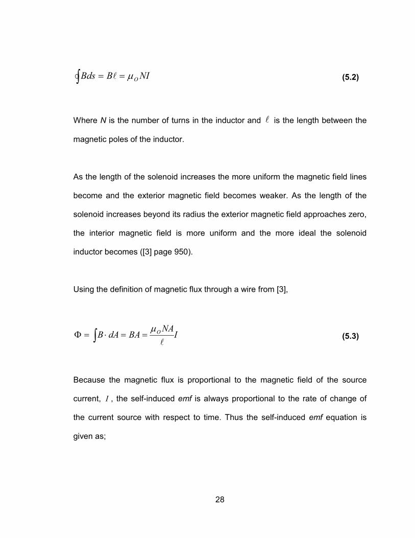
∫ == NIBBds Oµl (5.2)
Where N is the number of turns in the inductor and l is the length between the
magnetic poles of the inductor.
As the length of the solenoid increases the more uniform the magnetic field lines
become and the exterior magnetic field becomes weaker. As the length of the
solenoid increases beyond its radius the exterior magnetic field approaches zero,
the interior magnetic field is more uniform and the more ideal the solenoid
inductor becomes ([3] page 950).
Using the definition of magnetic flux through a wire from [3],
INA
BAdAB O∫ ==⋅=Φl
µ (5.3)
Because the magnetic flux is proportional to the magnetic field of the source
current, I , the self-induced emf is always proportional to the rate of change of
the current source with respect to time. Thus the self-induced emf equation is
given as;

29
dt
dIL
dt
dN −=
Φ−=ε (5.4)
where L is the inductance of the solenoid.
The inductance of the solenoid is therefore given as;
g
AN
I
NAB
I
NL
l
2µ==
Φ= (5.5)
where,
L , is the inductance
N , is the number of wire turns
I , is the DC current in the inductor
A , is the cross-sectional area of the inductor core
B , is the magnetic field
Φ , is the magnetic flux
µ , is the permeability of free space given as 4π x 10-7 Tm/A
gl , is the magnetic path length between the magnetic poles (also known as the
gap length in power inductors)

30
5.1 Air-Core Design
Using Equation 5.5, an inductor can be designed that meets the minimum 15 µH
described in the buck converter design section above. By making assumptions
about some of the parameters of the inductor, the design can be made simple.
Since the length of the inductor must be much greater than the radius, assuming
the inductor length is equal to the diameter of the inductor allows the length of
the inductor to be twice the radius and therefore satisfies the requirement and
simplifies the design. Also, the length of a tightly wound inductor is dependent on
the diameter of the wire used, multiplied by the number of turns used in the
inductor. This will allow the diameter of the wire to be determined once the
number of turns and required length of the inductor is found.
From Equation 5.5, it can be seen that the dominating term in determining the
inductance is the number of turns. Selecting a number of turns that when
squared and multiplied by the constant permeability of free space µ, mTe ⋅− 74π ,
closely approximates the required value of inductance; one can then use the
length of the solenoid inductor to tweak the inductance value to the required
magnitude. In selecting the number of turns, a balance must be made such that
the practicality of having too many turns using a small wire thickness will provide
too little structural support for the inductor component and too few turns that
would require the radius of the inductor to exceed the requirement that the length
of the solenoid inductor be much greater than the radius.

31
Therefore, assuming that 20=N , HL µ15= and that dr =≈ 2l (which
satisfies the requirement that the solenoid inductor length be much greater than
its radius), where d is the diameter of the inductor and l is its length.
Rearranging Equation 5.5 by solving for the cross-sectional area of the inductor,
as shown in Equation 5.6 below; the diameter of the inductor can be calculated
by substituting the cross-section area with its area equation yielding Equation
5.7, for the diameter of the inductor.
2
2
2
2 N
LdrA
µππ
l=
== (5.6)
22
N
Ld
πµl
= (5.7)
By adjusting the length of the inductor,l , the diameter becomes approximately
equal to the length of the inductor at 3.8 cm. Dividing the length of the inductor,
3.8 cm, by the number of turns, 20, produces a maximum wire diameter, Wd , of
1.9 mm. The closest wire diameter that would allow the 3.8 cm inductor length
and the number of turns conforms to the American Wire Gauge standard (AWG)
of 13 gauge wire. This gauge of wire has a standard 0.1828 cm diameter, which

32
will allow slight spacing between each turn and is thick enough to provide enough
current carrying capacity.
To determine the approximate length of 13 gauge wire needed to make the
inductor, the circumference of the solenoid inductor is calculated using the
equation, dc ⋅=π and multiplying the resulting 24 cm by the number of turns
gives an approximate length of 480 cm.
The resistance, r , of the inductor can now be calculated using the total length of
the wire, Wl , cross sectional area of the wire, WA , and the resistivity of copper,
m⋅Ω×= −81072.1ρ , in the equations;
222
cm026.04
)cm1828.0(
4≈==
ππ WW
dA (5.8)
mΩ 32m 100.026
cm4.8Ωm 101.724
8
=×
××== −
−
W
WL
AR
lρ (5.9)
From the above calculations, an air-core inductor seems to meet the needs of the
power supply, however, due to the DC current being as high as 25 A the air core
will saturate and not provide the required inductance. To overcome this limitation
a power inductor must be designed.

33
5.2 Iron Ferrite Design
Using an iron ferrite core will increase the saturation limit of the inductor allowing
higher DC current. A power inductor able to handle 25 ADC will be designed using
an iron ferrite core to increase magnetic field with fewer windings.
Figure 5.3 Hysteresis of Magnetics Inc. E-Core 45528.
The inductor core chosen is Magnetics Inc. 45528-EC E-Core. The Magnetic
Hysteresis Graph of the core made of Magnetics Inc. R Material is shown in
Figure 5.3. Using this graph the maximum magnetic field of this core before
saturation is estimated at 0.3 Telsa (3 Kilogauss). The cross sectional area of the
core is given by the manufacturer as 3.61 cm2 (0.000361 m2). Rearranging
Equation 5.5, the number of turns can be calculated as:

34
turns15.4)3.0)(000361.0(
)30)(1015( 6
=×
==−
AB
LIN (5.10)
Allowing the number of turns to be 4, the required gap length between the
magnetic poles can be calculated using Equation 5.5 as:
m000484.01015
)000361.0)(4)(104(6
272
=×
×==
−
−πµL
AN COgl (5.11)
The energy stored in the inductor is
∫∫ ∫ ====II
LIIdILLIdIdUU0
2
02
1
==
===
=−−
−−
J 1017)25.1)(1015)(5.0(
J107.4)25)(1015)(5.0(
2
1
2
1
626
326
2
2
xxU
xxU
LI
LI
MIN
MAX
MIN
MAX
(5.12)
The length of wire required for the 4 turns can be approximated by multiplying the
perimeter length of the square E-Core by the number of turns, which gives the
length of wire around the core as:
m468.0)021.00375.0)(4(2)(2 21 =+=+= SSNWl (5.13)

35
Adding 0.05 m to the length of the wire for the leads of the inductor yields a total
wire length of 0.518 m (20.4 inches). The resistivity of the wire can be calculated
to be:
Ω=×
×Ω×== −
−
m7.2m100331.0
m518.0m1072.14
8
W
WL
AR
lρ (5.14)
From the manufacturer the core power loss can be calculated as:
DC
L BafP = (5.15)
Where,
LP , is the core power loss (milliwatt) per cubic centimeter
a , is 0.036 for R material
B , is the magnetic flux density (in kilogauss)
D , is 2.68 for R material
Since B is 3 kG at 30 A then the power loss is:
mW/ccm1300)3)(100)(036.0( 68.264.1 ≈=LMAXP (5.16)
Since the volume of the core (per the manufacturer’s specifications) is about 88
ccm (for two E-Core’s) the power dissipated by the core is:
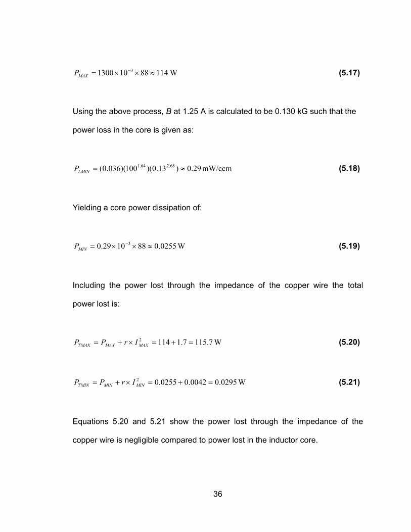
36
W11488101300 3 ≈××= −MAXP (5.17)
Using the above process, B at 1.25 A is calculated to be 0.130 kG such that the
power loss in the core is given as:
mW/ccm29.0)13.0)(100)(036.0( 68.264.1 ≈=LMINP (5.18)
Yielding a core power dissipation of:
W0255.0881029.0 3 ≈××= −MINP (5.19)
Including the power lost through the impedance of the copper wire the total
power lost is:
W7.1157.11142 =+=×+= MAXMAXTMAX IrPP (5.20)
W0295.00042.00255.02 =+=×+= MINMINTMIN IrPP (5.21)
Equations 5.20 and 5.21 show the power lost through the impedance of the
copper wire is negligible compared to power lost in the inductor core.
37
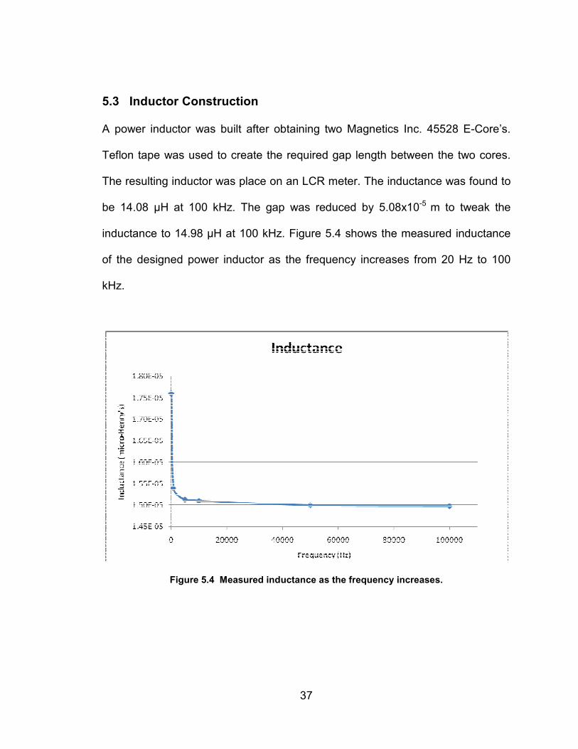
5.3 Inductor Construction
A power inductor was built after obtaining two Magnetics Inc. 45528 E-Core’s.
Teflon tape was used to create the required gap length between the two cores.
The resulting inductor was place on an LCR meter. The inductance was found to
be 14.08 µH at 100 kHz. The gap was reduced by 5.08x10⁻⁵ m to tweak the
inductance to 14.98 µH at 100 kHz. Figure 5.4 shows the measured inductance
of the designed power inductor as the frequency increases from 20 Hz to 100
kHz.
Figure 5.4 Measured inductance as the frequency increases.

38
Chapter 6 Analog Simulation
In the following simulations the switching networks will be modeled based on the
simple buck converter. The simulations will be used to demonstrate the behavior
of the above designed buck converter and to derive a controller or compensator
to regulate the output of the converter through changes in load and input voltage.
The compensated buck converter will later be used to simulate the digital buck
converter.
6.1 Output Stage Simulation Design
Using Matlab/Simulink, a model was created of a buck converter having a 15 µH
inductor whose resistance is 0.0027 Ω and a 33 µF capacitor who’s ESR is 0.055
Ω. Figure 6.1 shows the relative location of the resistive elements of the inductor
and capacitor.
39
SupplyC
L
LOAD
Q1
Q2
RL
Resr
Figure 6.1 Buck converter model showing resistive elements of the inductor and
capacitor.
Using the equations for the voltage across an inductor, dt
diLV L= ; the current in a
capacitor, dt
dvCI C= ; and the output voltage, )( OLESRCO iiRVV ++= a
mathematical model of a buck converter was derived and is represented by the
following equations:
40
( )OLLIL VRIDVLS
I −−×
×
=11
(6.1)
( )OLC IICS
V −×
×
=11
(6.2)
)( OLESRCO IIRVV ++= (6.3)
=
L
OOUT
R
VI (6.4)
where
LI , current through the inductor
CV , voltage across the capacitor
LR , resistor of the inductor
ESRR , Equivalent Series Resistance of the capacitor
OV , output voltage of the buck converter
INV , voltage input of the buck converter
OI , current output of the buck converter
D, duty cycle

41
Using these equations a Simulink model of the buck converter was constructed
to use throughout the remainder of this document, Figure 6.2.
2
IL
1
Vo
Product
1
s
1
s
.055
1/33e-6
1/15e-6
.0027
3
I_out
2
D
1
Vs
Figure 6.2 Simulink model of the buck converter output stage.
6.2 PWM Design
The Pulse Width Modulator (PWM) was designed based off the functional block
diagram of Figure 2.1. A saw-tooth waveform is compared to the feedback error
of the system output as shown in Figure 2.2. In the PWM model of Figure 6.3, the
error input is limited from 0.01 to 7.99. This has the effect of producing dead time
in the resulting pulse width output. The signal from the comparator is then
converter to a double to ensure compatibility with the downstream functional
blocks.

42
1
Pulse
Sawtooth<= double
1
Error
Figure 6.3 The Simulink model of a simple PWM.
The DC control voltage-to-duty cycle transfer function, TM, can be derived from
the equation [1];
TMC
MVV
DT
1=≡ (6.5)
where VTM is the magnitude of the saw-tooth waveform detailed in [1]. In the
PWM model above VTM is 8, therefore TM is 0.125.
6.4 Open Loop Transfer Functions
The circuit diagram in Figure 6.4 shows the small signal diagram used to
linearize the switching network and derive the transfer functions needed to
analysis the system.

43
Figure 6.4 Small signal model of a buck converter [1].
The buck converter output stage transfer function can be derived by equating the
impedances of the inductor, capacitor and load resistance as a resistive network
shown in the Figure 6.5 and 6.6. The inductor impedance, r, has been neglected
due to its minimal impact on the system whereas the capacitors ESR will produce
a zero in the transfer function shown in Equation 6.7.
rC
C
R
L
VI
IL
Figure 6.5 Output stage of the buck converter.

44
Figure 6.6 Impedance equivalent of the output stage shown in Figure 6.5.
The impedances Z1 and Z2 are given as:
sLsZ ×== H151 µ (6.6)
( ) 1)104.8(
1)102()2.0(
1
1
1
)1
(
)(||6
6
2 +×
+×=
++×
+=
++
+=+=
−
−
s
s
rRsC
CsrR
sCrR
sCrR
CrRZC
C
C
C
C (6.7)
Substituting the impedances into the following equation gives the output power
stage transfer function as:
932
93
6102
6
221
2
102)1012(
102)104(
1)106()105(
1)102(
11
1
×+×+
×+×=
+×+×
+×=
+
++
+
+=
+=
−−
−
ss
s
ss
s
CrR
Ls
R
rLCs
Csr
ZZ
Z
V
V
CC
C
I
O
(6.8)

45
Where, H15µ=L , F33µ=C , Ω= 055.0Cr , and Ω= 4R
From the above figure it is noted that the output impedance, ZO, of the buck
converter is given as:
( ) 1)10134(
1)102()4(
1
1)(||
6
6
20 +×
+×=
++×
+=+==
−
−
s
s
rRsC
CsrRCrRZZ
C
C
C (6.9)
Due to variations in internal components and environments the duty of the PWM
may vary about the intended duty cycle such that the duty cycle can be
represented by the equation:
dDDT += (6.10)
Where d is the change in the intended or ideal duty cycle, D.
Using Equation 6.10, the input voltage can be represented as:
)( dDVV sI += (6.11)
where Vs is the input voltage of the buck converter.

46
Substituting Equation 6.10 into Equation 6.8 yields the open loop input-to-output
voltage transfer function (also known as Audio Susceptibility):
932
93
21
2
102)105.11(
102)104()()(
×+×+
×+×=
++==
ss
sD
ZZ
ZdD
V
VM
s
O (6.12)
Where d is assumed to be zero.
The control-to-output transfer function (also known as the duty ratio-to-output
transfer function) [1] can be derived from the small-signal model in Figure 6.4.
OLO Ziv = (6.13)
LSOOSLL sLidVvvdVsLiv −=→−== (6.14)
The DC or average voltage on the input lead of the inductor, L, is VsD which is
equal to VO such that the DC or average voltage across the inductor is zero;
neglecting the inductor resistance. From this, the voltage across the inductor is
only due to the change in the duty cycle, d.
Equating vo:
L
OLOLOi
viZiv == (6.15)

47
O
SL
ZsL
dVi
+= (6.16)
O
SL
ZsL
V
d
i
+= (6.17)
Substituting Equation 6.9 and 6.17 into Equation 6.15 yields the control-to-output
transfer function (also known as duty ratio-to-output transfer function) [1].
( )
( ) 22
2
4
5
932
93
6102
6
2
2
2
1047.42000
105
102)104(
102)104()12(
1)102(105
1)102()12(
1
1
OO
OO
C
C
C
S
O
O
SO
LO
P
ss
sA
js
s
ss
s
ss
s
CsrR
RrLCs
CsrV
ZsL
ZVZ
d
i
d
vT
ωξω
ωξω
++
+=
×±+
×+=
×+×+
×+×=
+×+×
+×=
++
+
+=
+===
−−
−
(6.18)
Where,
ξ , dampening ratio
Oω , is the natural frequency of the system
The natural frequency of the transfer function, TP, is given as:
48
Hz71212
rad/sec700,4492 ==⇒≅=π
ωω O
OO fe (6.19)
The damping ratio is given as:
134.080000
3175
2
2===
O
O
ωξω
ξ (6.20)
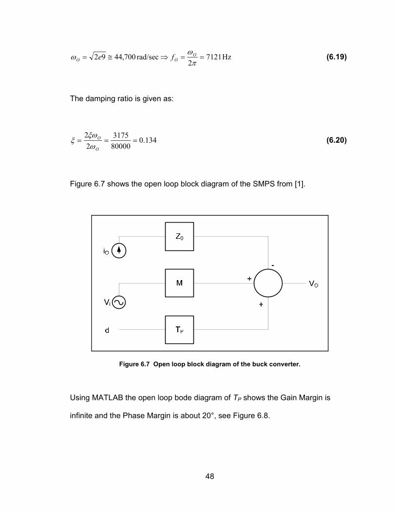
Figure 6.7 shows the open loop block diagram of the SMPS from [1].
Figure 6.7 Open loop block diagram of the buck converter.
Using MATLAB the open loop bode diagram of TP shows the Gain Margin is
infinite and the Phase Margin is about 20°, see Figure 6.8.

49
-50
0
50
Magnitu
de (
dB
)
103
104
105
106
107
-180
-135
-90
-45
0
Phase (
deg)
Bode Diagram
Gm = Inf , Pm = 19.8 deg (at 1.65e+005 rad/sec)
Frequency (rad/sec)
Figure 6.8 Bode diagram of the buck converter of transfer function, TP, without
compensation.
50
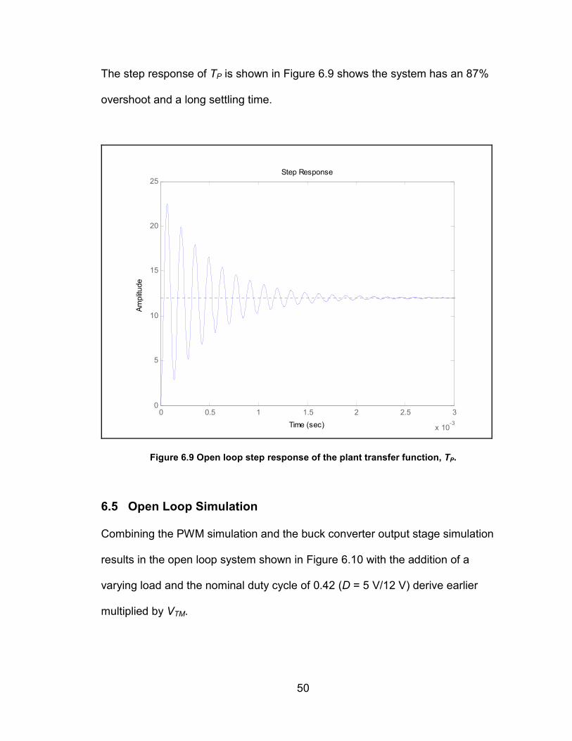
The step response of TP is shown in Figure 6.9 shows the system has an 87%
overshoot and a long settling time.
0 0.5 1 1.5 2 2.5 3
x 10-3
0
5
10
15
20
25
Step Response
Time (sec)
Am
plit
ude
Figure 6.9 Open loop step response of the plant transfer function, TP.
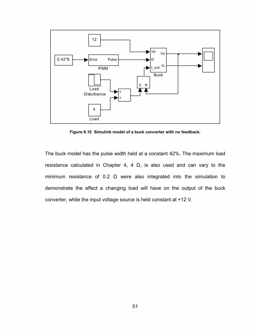
6.5 Open Loop Simulation
Combining the PWM simulation and the buck converter output stage simulation
results in the open loop system shown in Figure 6.10 with the addition of a
varying load and the nominal duty cycle of 0.42 (D = 5 V/12 V) derive earlier
multiplied by VTM.
51
Error Pulse
PWM
Load
Disturbance
4
Load
0.42*8
12
Vs
D
I_out
Vo
IL
Buck
Figure 6.10 Simulink model of a buck converter with no feedback.
The buck model has the pulse width held at a constant 42%. The maximum load
resistance calculated in Chapter 4, 4 Ω, is also used and can vary to the
minimum resistance of 0.2 Ω were also integrated into the simulation to
demonstrate the affect a changing load will have on the output of the buck
converter, while the input voltage source is held constant at +12 V.

52
0 0.5 1 1.5
x 10-3
0
5
10Output Voltage of Buck Converter
Voltage (
V)
0 0.5 1 1.5
x 10-3
-10
0
10
20
30
Time (sec)
Curr
ent
(A)
Output Current of Buck Converter
IO
VO
R
Figure 6.11 Plot of buck converter voltage and current output with changing load.
As shown in Figure 6.11 as the load changes the output of the buck converter
varies. Also, when the load resistance, R, changes from the maximum resistance
of 4 Ω to the minimum resistance of 0.2 Ω, the current also changes from the
design specified minimum output current, IOMIN, of 1.25 A to the maximum output
current, IOMAX, of 25 A.
6.5 Closed loop
Incorporating a feedback loop into the design allows for correction of the output
when variables alter. The feedback of the output voltage is scaled down and

53
compared to a reference voltage. It will be assumed that the output of the buck
converter will be compared to a 2 V reference therefore resulting in the output
voltage, nominally 5 V, to be scaled by a gain of 0.4. The feedback gain of the
closed loop system becomes:
4.05
2==≈
O
R
V
VB (6.21)
The transfer function of the pulse-width modulator, the buck converter, and the
feedback network gain is the uncompensated loop gain which is given as:
932
93
102104
102104)6.0(
×+×+
×+×==
ss
sTTT PMK β (6.22)
The open-loop step response and bode plot of Tk are given as:

54
0 0.5 1 1.5 2 2.5 3
x 10-3
0
0.2
0.4
0.6
0.8
1
1.2
1.4Step Response
Time (sec)
Am
plit
ude
Figure 6.12 Open loop step response of TK.
-80
-60
-40
-20
0
20
Magnitu
de (
dB
)
103
104
105
106
107
-180
-135
-90
-45
0
Phase (
deg)
Bode Diagram
Gm = Inf , Pm = 17.2 deg (at 5.65e+004 rad/sec)
Frequency (rad/sec)
Figure 6.13 Bode plot of TK.
55
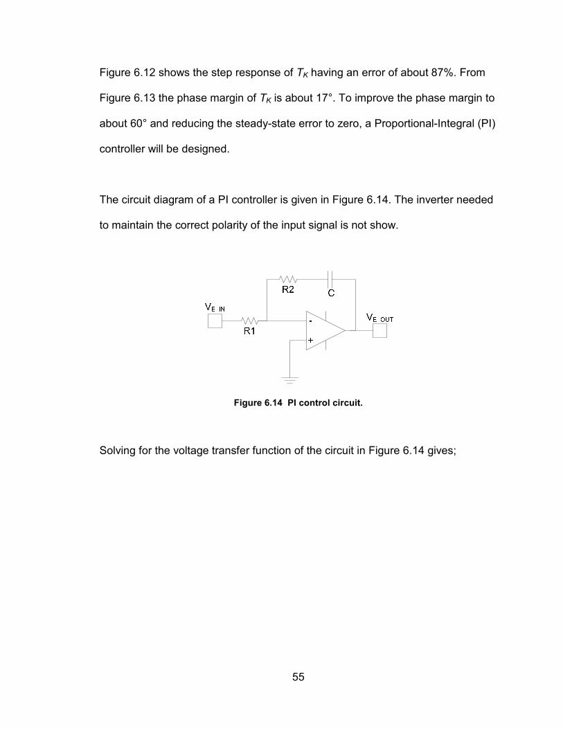
Figure 6.12 shows the step response of TK having an error of about 87%. From
Figure 6.13 the phase margin of TK is about 17°. To improve the phase margin to
about 60° and reducing the steady-state error to zero, a Proportional-Integral (PI)
controller will be designed.
The circuit diagram of a PI controller is given in Figure 6.14. The inverter needed
to maintain the correct polarity of the input signal is not show.
Figure 6.14 PI control circuit.
Solving for the voltage transfer function of the circuit in Figure 6.14 gives;

56
CRK
R
RK
s
sK
KK
s
KK
CsRR
R
V
VsT
R
sCR
VV
sCR
V
R
V
I
P
I
PI
IP
INE
OUTE
x
INEOUTE
OUTEINE
1
1
2
11
2
_
_
1
2
__
2
_
1
_
1
11
)(
1
1
=∴
=∴
+−
=
+−=
+−==
+=−⇒
+−=
(6.23)
Applying the inverter, the control transfer function becomes;
s
sK
KK
s
KK
CsRR
R
V
VTAT
I
PI
IP
INE
OUTE
xIC
+
=
+=
+===
11
11
2
_
_ (6.24)
where AI is -1.
Adjusting the magnitude curve of the uncompensated transfer function, TK, by
14.5 dB at the desired crossover frequency ( sec/rad1061.4 4' ×=gw ), a desired
phase margin of about 60° can be achieved. The gain KP can be used to adjust
the gain by 14.5 dB using the following from [6];
PdB
g KjwG log20)( ' −= (6.25)

57
Solving for KP gives the equation:
1883.01010 )20/5.14()20/)(( === −−dB
jwG
PK (6.26)
If the corner frequency PI KKw /= is positioned well below '
gw , the phase lag of
the PI controller will have a negligible effect on the phase of the compensated
system near '
gw . As a general guideline, PI KK / should be one to two decades
below '
gw [6]. Therefore, the gain KI of the PI compensator can be calculated by:
86810
1061.41883.0
10
4'
=×
×== g
PI
wKK (6.27)
The control transfer function becomes;
s
s
s
s
s
sK
KK
TI
PI
C
8681883.0868
1883.018681
+=
+×=
+
= (6.28)
The bode plot of the controller transfer function is given as;

58
-20
-10
0
10
20
Magnitu
de (
dB
)
102
103
104
105
-90
-45
0
Phase (
deg)
Bode Diagram
Frequency (rad/sec)
Figure 6.15 Bode plot of TC.
Using the controller transfer function, TC, the loop gain, T, is given as;
)105.42000(
)4610()105(
1024000
1011028.2452
8681883.0
102104
102104)6.0(
4
5
923
1282
932
93
×±+
+×+=
×++
×+×+=
+
×+×+
×+×==
jss
ss
sss
ss
s
s
ss
sTTTT CPM β
(6.29)
The bode plot of, T, is given as;

59
-100
-80
-60
-40
-20
0
20
Magnitu
de (
dB
)
102
103
104
105
106
107
-180
-135
-90
-45
0
Phase (
deg)
Bode Diagram
Gm = Inf , Pm = 53.7 deg (at 4.62e+004 rad/sec)
Frequency (rad/sec)
Figure 6.16 Bode plot of T.
Nyquist Diagram
Real Axis
Imagin
ary
Axis
-1 -0.8 -0.6 -0.4 -0.2 0 0.2 0.4 0.6 0.8-2
-1.5
-1
-0.5
0
0.5
1
1.5
2
System: T
Phase Margin (deg): 53.7
Delay Margin (sec): 2.03e-005
At frequency (rad/sec): 4.62e+004
Closed Loop Stable? Yes
Figure 6.17 Nyquist diagram of T confirms the Phase Margin in Figure 6.16.

60
Figure 6.16 shows the phase margin of the open-loop compensated system as
approximately 54°. Figure 6.17 confirms the phase margin since the Bode plot of
Figure 6.16 has multiple crossover frequencies.
The closed-loop transfer function of the compensated system is given as;
)468)(107.41992(
)4610)(105(
101102.24452
1011028.2452
868)1883.0(
102)104(
102)104()6.0(
1
4
5
12923
1282
932
93
+×±+
+×+=
×+×++
×+×+=
+
×+×+
×+×=
+=
sjs
ss
sss
ss
s
s
ss
s
TTT
TTTT
CPM
CPM
cl ββ
(6.30)
Where the corner frequencies of the closed-loop compensated system are at w1
= 468 rad/sec (74.52 Hz), w2 = 4610 rad/sec (734 Hz), w3 = 46773 rad/sec (7447
Hz, complex pole) and w4 = 5x10⁵ rad/sec (79617 Hz).
The step response of TCL is given as:

61
Step Response
Time (sec)
Am
plit
ude
0 0.002 0.004 0.006 0.008 0.01 0.0120
0.1
0.2
0.3
0.4
0.5
0.6
0.7
0.8
0.9
1
System: Tcl
Rise Time (sec): 0.00466
Figure 6.18 Step response of TCL.
101
102
103
104
105
106
107
-180
-135
-90
-45
0
Phase (
deg)
Bode Diagram
Frequency (rad/sec)
-100
-80
-60
-40
-20
0
20
Magnitu
de (
dB
)
-3.04 dB at 472 rad/sec
Figure 6.19 Bode diagram of Tcl.

62
The bandwidth of the closed loop system was calculated by Matlab to be 472
rad/sec (75.16 Hz). This bandwidth calculation can be confirmed from the bode
plot of Figure 8.19 at a gain of -3 dB (or 0.7079) below the first crossover
frequency. This first crossover frequency happens to be very close to the first
corner frequency from Equation 6.30 of 468 rad/sec (74.52 Hz). Figure 6.19
shows that at 472 rad/sec (75.16 Hz) the gain is -3.04 dB (or 0.7047).
Assuming C1 to be 0.1 µF, R1 of Figure 6.14 can be found by;
kΩ5.11101.0868
1161 =
××==
−CKR
I
(6.31)
Using R1, R2 can be found by;
Ω≈=××== k2200Ω2165105.111883.0 3
12 RKR P (6.32)
The closed-loop blocked diagram of the system is shown in Figure 6.20 [1].

63
Figure 6.20 Closed loop block diagram of the buck converter.
The designed controller, TC, was incorporated in the model and shown in Figure
6.21.
Error Pulse
PWM
0.1883s+868
s
PI Controller
Load
Disturbance
4
Load
2.0
12
0.4
Vs
D
I_out
Vo
IL
Buck
Figure 6.21 Buck converter with feedback.

64
Figure 6.22 shows the response of the system Simulink buck model of Figure
6.21. As the load changes the feedback causes the output voltage to be returned
to the desired 5 V and the output current is increased from 1.25 A to 25 A.
0 0.005 0.01 0.0150
2
4
6Output Voltage of Buck Converter
Voltage (
V)
0 0.005 0.01 0.015-10
0
10
20
30Output Current of Buck Converter
Curr
ent
(A)
Time (sec)
VO
R
IO
Figure 6.22 Plot of the buck converter voltage output with feedback while the load varies.
Overlaying the step response of Figure 6.18 and the response from the Simulink
model, in Figure 6.21, shows, in Figure 6.23, that the two systems have nearly
identical responses.

65
Step Response
Time (sec)
Am
plit
ude
1 2 3 4 5 6 7 8 9 10 11
x 10-3
0.5
1
1.5
2
2.5
3
3.5
4
4.5
5
System: Tcl
Rise Time (sec): 0.00466
System: Tcl
Final Value: 5
Figure 6.23 Scaled plot in Figure 6.15 overlaid on the output of the buck converter model.
1.3355 1.336 1.3365 1.337 1.3375 1.338
x 10-3
4.94
4.96
4.98
5
5.02
5.04
Time (sec)
Voltage (
V)
Figure 6.24 Ripple voltage of the buck output voltage.

66
The ripple voltage produced in the SMPS model from the charging and
discharging of the inductor and capacitor can be seen in Figure 6.24, above.
Measuring the ripple voltage from Figure 6.24, it can be seen that the output
ripple voltage from the model is approximately 110 mV where the maximum
allowable ripple voltage is 0.25 V. Using Equation 2.2, the ripple voltage is
calculated to be about 182 mV.
The closed-loop input-to-output voltage (audio susceptibility) is given by the
equation [1]:
21182133945
18213394
102105.4106.31028.416000
104106.11024000
1
×+×+×+×++
×+×+×+=
+=
sssss
ssss
T
MM CL
(6.32)
The bode plot of the closed loop audio susceptibility can be seen in Figure 6.25.

67
-80
-60
-40
-20
0
20
Magnitu
de (
dB
)
101
102
103
104
105
106
107
-180
-90
0
90
Phase
(deg)
Bode Diagram
Frequency (rad/sec)
Figure 6.25 A bode plot of the closed loop audio susceptibility.
The step response of the closed loop audio susceptibility can be seen in Figure
6.26. The step response shows when the input voltage of the buck converter is
disturbed by a 1 V step response the output of the buck converter will transition
in the direction of the step response to a peak of about 1.5 V, then oscillate about
0.8 V and settle to intended output voltage, having an error of 0 V.

68
0 0.005 0.01 0.0150
0.5
1
1.5
Step Response
Time (sec)
Am
plit
ude
Figure 6.26 Audio susceptibility due to a unit step disturbance on the input voltage.
A negative unit step disturbance was incorporated into the closed loop buck
model. Figure 6.27 shows the response of the model having an initial transient
response to about 4.6 V and then settling to zero error as predicted in Figure
6.26.

69
0 0.002 0.004 0.006 0.008 0.01 0.012 0.014 0.016 0.018 0.020
5
10
12
VO
VS
Figure 6.27 Unit step response disturbance on the input voltage of the buck model.
6.6 Buck Design Implementation
A prototype of the above analog buck converter was constructed to demonstrate
the design’s viability. Using a LM555 Timer, a ramp generator was created to
compare to the feedback signal from the output of the buck converter. The
schematic shown in Figure 6.28 is of a simple buck converter design, using a
TIP3055 Power NPN Transistor as the “high side” switch and a 1N5417 Power
Diode as the “low side” switch. UC1707 is a power BJT/MOSFET Driver used to
provide enough current to overcome the gate capacitance of the power BJT
causing the transistor to switch states in a timely manner. The output load, R,
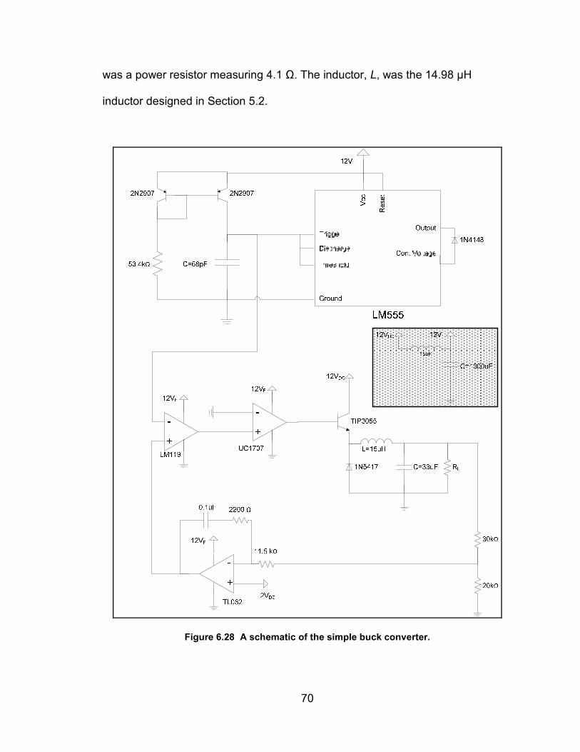
70
was a power resistor measuring 4.1 Ω. The inductor, L, was the 14.98 µH
inductor designed in Section 5.2.
Figure 6.28 A schematic of the simple buck converter.

71
Figure 6.29 shows the steady state output of the simple buck converter from
Figure 6.28. It can be seen that the output shown on channel 4 had a ripple
voltage of approximately 0.196 V which was less than the maximum 0.25 V ripple
voltage design specification. The measurement window of the Figure 6.26 shows
the DC output is 5.003 V at a frequency of 100 kHz. The periodic noise on the
output signal (channel 4) was due to the switching signal (channel 3) from the
UC1707 driver. The input power was measured to be 14.87 W and the output
power was found to be 6.098 W resulting in an efficiency of about 41% for the
simple buck converter. Note the voltage ripple on the output (channel 4) rises
when the switching signal (channel 3) was high. This was not the case for the
following synchronous buck converter.

72
Figure 6.29 Recorded signals from the simple buck converter. Channel 1 is the ramp
signal, channel 2 is the feedback signal, channel 3 is the switching signal, and channel 4 is
the output of the buck converter.

73
Using the same PWM as above, a synchronous buck converter was created
using an IRF9Z34N Power P-channel MOSFET as the “high side” switch and an
IRF510 Power N-channel MOSFET as the “low side” switch. The UC1707 driver
has two channels set up to switch in the same polarity. Using the same polarity
signal to drive the N and P-channel MOSFET transistors caused the P-channel
transistor to be off when the N-channel transistor was on and the P-channel
transistor was on when the N-channel transistor is off.

74
C=68pF
TriggerOutput
Vcc
DischargeCon. Voltage
Re
set
Threshold
LM555
Ground
2N2907
1N4148
12VF
LM119
+
-
12VF
L=15uH
C=33uF RL
12VDC
30kΩ
20kΩ
TL082
+
-
12VF
11.5 kΩ
0.1uF
IRF9Z34N
2VDC
53.4kΩ
IRF510
UC1707
+
-
12VF
+
-
12VF
12VF
C=1000uF
12VDC
15uF
2N2907
2200 Ω
Figure 6.30 A schematic of the synchronous buck converter.

75
Figure 6.31 shows the steady-state output of the synchronous buck converter.
The switching signal (channel 3) was opposite of the switching signal in Figure
6.29. This was due to the P-channel MOSFET being the high side transistor. The
load of the synchronous buck converter was a 4.1 Ω power resistor. The output
power was 6.098 W; whereas the input power was 7.437 W. This is an efficiency
of about 82% compared to the design estimate of 85% given in Chapter 3.
Channel 4 showed the output of the synchronous buck converter had a ripple
voltage of 0.15 V at 102 kHz.

76
Figure 6.31 Recorded signals from the synchronous buck converter. Channel 1 is the
feedback voltage, channel 2 is the ramp signal, channel 3 is the switching signal, and
channel 4 is the output voltage.

77
Figure 6.32 shows the output of the synchronous buck converter when the load
impedance was switched from 4.1 Ω to 1 Ω. The input current to the buck
converter changed from about 0.62 A to about 3.25 A. This resulted in an error of
about 1.3% (0.065 V) in the intended 5 V output shown in Figure 6.32. The load
could not be switched fast enough to recreate the transient response shown in
the Matlab simulations due to component limitations.
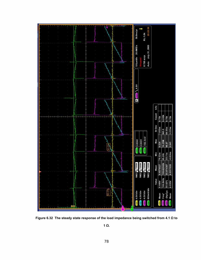
78
Figure 6.32 The steady state response of the load impedance being switched from 4.1 Ω to
1 Ω.

79
Chapter 7 Digital Switch Mode Power Supply Design
Digital switch mode power supplies (also known as digital power supplies)
incorporate a microcontroller in place of the analog PWM discussed earlier.
These microcontrollers can implement complex intelligent control schemes such
as digital control, fuzzy logic control, and state-space control schemes ([7], [8],
and [9]).
Digital power supplies allow for flexibility in design components due to the ability
to tweak the power supply output through the programmed control scheme
instead of exchanging hardware components to obtain a satisfactory output. This
also allows fewer design iterations, thus speeding the design to production.
Digital power supplies can make adjustments for nonlinearities and aging affects
in hardware components. They can also be reprogrammed to implement different
control schemes determined by the operator through a data bus from the Central
Processing Unit (CPU) to the microcontroller within the SMPS.
A simplistic view of a digital buck DC-DC converter can be in Figure 19, below.
This digital power supply is very similar to the SMPS discussed in the ‘Analog
Design’ section above with the exception that the PWM has been replaced with a
microcontroller and associated memory. The pulse width signal is produced by a
microcontroller and amplified by the driver circuitry.

80
Figure 7.1 A simplified functional diagram of a digital buck DC-DC converter.
The microcontroller used in a digital power supply requires a source of power
often derived from a regulating zener diode or linear power supply. This
microcontroller is used solely for control over the power supply output and
consumes power from continuous operation, memory, and processing.
Using Matlab/Simulink, a model of a digital power supply, shown in Figure 7.2,
was created using the same buck converter design discussed in Chapter 6 to
demonstrate the operation of a digital power supply. An error signal is created
using a gain of 0.4, summing block and a constant block representing a
reference voltage of 2 V. The resulting signal is put through an Analog-to-Digital

81
converter (A/D converter) represented by the transient delay block, zero-order
hold block, and the A/D quantizer. The processor is represented by a discrete
transfer function, which is the Z-transform of PI controller developed in Chapter
6. The resulting signal is then passed through a Digital-to-Analog converter (D/A
converter) using a Digital-to-Analog quantizer block.
The Bilinear Z-transformer of can be derived from an integral [9]:
∫−=t
ECC dttvKvtv0
)()0()( (7.1)
Using the trapezoidal rule to discretize Equation 7.1 which is:
2
))1(()())1((
)())1(()()1(
TnvnTvTKTnv
duuvKTnvnTv
EE
C
nT
Tn
ECC
−+−−≈
−−= ∫−
(7.2)
In the Z-domain the equation 7.2 becomes:
[ ])()(2
)()( 11 zvzzvT
Kzvzzv EECC
−− +−= (7.3)
Solving for the transfer function yeilds:
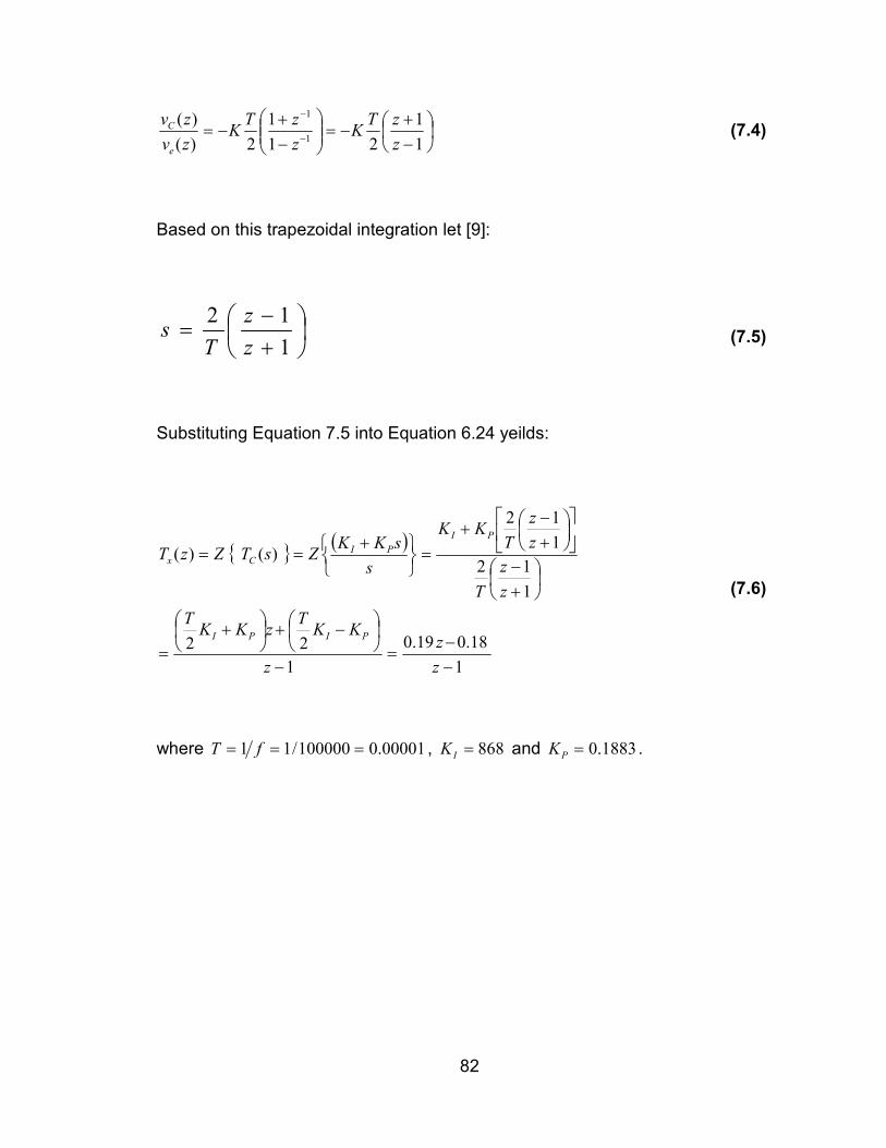
82
−
+−=
−
+−=
−
−
1
1
21
1
2)(
)(1
1
z
zTK
z
zTK
zv
zv
e
C (7.4)
Based on this trapezoidal integration let [9]:
+
−=
1
12
z
z
Ts (7.5)
Substituting Equation 7.5 into Equation 6.24 yeilds:
( )
1
18.019.0
1
22
1
12
1
12
)()(
−
−=
−
−+
+=
+
−
+
−+
=
+
==
z
z
z
KKT
zKKT
z
z
T
z
z
TKK
s
sKKZsTZzT
PIPI
PI
PICx
(7.6)
where 00001.0100000/11 === fT , 868=IK and 1883.0=PK .

83
Zero-Order
Hold
2
Vref
Error Pulse
PWM
4
Load
12
Input Voltage
.4
0.19z-0.18
z-1
Discrete
Transfer Fcn
Delay
DPWM
limits
DPWM
Quantizer
Vs
d
Iout
Vo
IL
Buck
A/D
Quantizer
A/D
Limits
Figure 7.2 A Simulink model of the buck converter with Digital feedback control.
Changing the load from 4 Ω to 0.2 Ω as in the analog design above, the digital
control loop maintains the output of the power supply. Figure 7.3 shows the
response of the digital control loop when the load resistance is changed from 4 Ω
to 0.2 Ω.
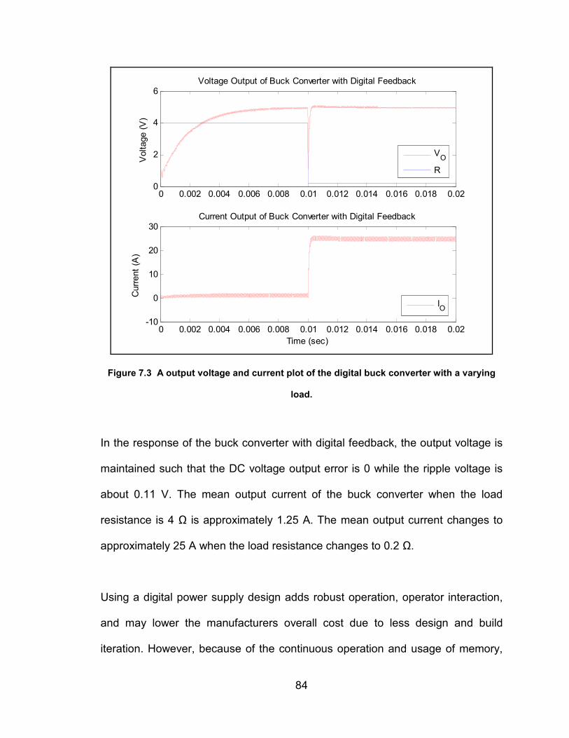
84
0 0.002 0.004 0.006 0.008 0.01 0.012 0.014 0.016 0.018 0.020
2
4
6
Voltage (
V)
Voltage Output of Buck Converter with Digital Feedback
0 0.002 0.004 0.006 0.008 0.01 0.012 0.014 0.016 0.018 0.02-10
0
10
20
30Current Output of Buck Converter with Digital Feedback
Time (sec)
Curr
ent
(A)
VO
R
IO
Figure 7.3 A output voltage and current plot of the digital buck converter with a varying
load.
In the response of the buck converter with digital feedback, the output voltage is
maintained such that the DC voltage output error is 0 while the ripple voltage is
about 0.11 V. The mean output current of the buck converter when the load
resistance is 4 Ω is approximately 1.25 A. The mean output current changes to
approximately 25 A when the load resistance changes to 0.2 Ω.
Using a digital power supply design adds robust operation, operator interaction,
and may lower the manufacturers overall cost due to less design and build
iteration. However, because of the continuous operation and usage of memory,

85
the digital power supply fails to compete with the efficiency of an analog power
supply design, [7].

86
Chapter 8 Modified Switch Mode Power Supply Design
Using concepts from both the analog design and digital design a switch mode
power supply can be created that combines the advantages of intelligent control
and the efficiency of analog control.
In Figure 8.1, below, a buck converter can been seen whose output can be used
to power a Central Processing Unit (CPU). This figure also shows a pulse width
modulator has been modified to accept commands from the CPU to alter the
initial setup of the pulse width scheme.
Until the CPU is functional, the MPWM (Modified Pulse Width Modulator) will
operate as discussed above in the ‘Analog Design’ section, see Figure 8.1. Once
the CPU is operational or out of reset it can run algorithms that calculate the
output ripple voltage and DC output voltage of the converter and the determine
best means of altering the output to suit the needs of the system by altering the
switching frequency, the DC offset and other various aspects, see Figure 8.2.

87
Fe
ed
ba
ck
No
Po
we
r a
t S
tart
-Up
No
Po
we
r a
t S
tart
-Up
LO
AD
Pu
lse
s
Figure 8.1 A SMPS with analog control at start-up using MPWM.
Figure 8.2 The CPU is out of reset and able to adjust aspects of the buck converter.

88
This MPWM – a functional diagram shown in Figure 8.3 below – contains a
Voltage Controlled Oscillator (VCO) that is setup to output a center (or base)
frequency until commanded to do otherwise by the CPU. The CPU can adjust the
output frequency of the VCO to tweak in the output ripple voltage of the buck
converter to meet the needs of the system.
The MPWM can also accept commands to adjust the DC output level of the buck
converter. Adjusting the reference voltage within the MPWM will result in the
buck converter DC output voltage to increase or decrease.
Three optional control features can be implemented to add to the level of control
the CPU has over the buck converter. The first is to limit the output level of the
pulse width signal to only what is required to properly switch transistors Q1 and
Q2. The second is the ability to adjust the phase between the pulse width signal
for Q1 and Q2 to increase or decrease the dead time of the PWM switching. The
MPWM can also be made to allow the SMPS output mode to be changed from
continuous to discontinuous by altering the frequency in which transistors Q1 and
Q2 are switched.
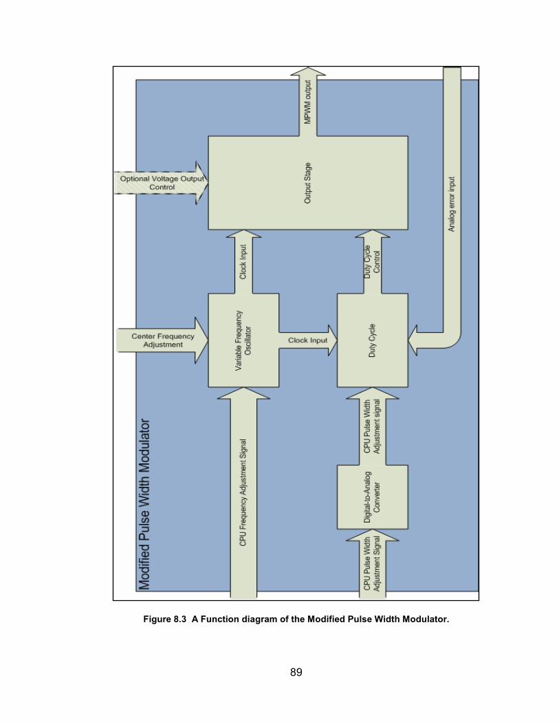
89
Figure 8.3 A Function diagram of the Modified Pulse Width Modulator.

90
A model of the MPWM, see Figure 8.4, was created and inserted into the model
with the buck converter - see Figure 8.5 - in Matlab/Simulink to demonstrate the
functionality of the MPWM. This model contains a voltage controlled oscillator
(VCO) whose center frequency is set to 100 kHz and an addition block to alter
the 2 V reference for feedback comparison. Also, an M-file S-function block was
inserted and programmed to simulate a CPU (or other intelligent source) able to
make adjustments to the MPWM based on the output of the buck converter.
2
Vor
1
d
Fdelta Fsaw
VCO
<=8
Add
4
Vr
3
Vrdelta
2
Fdelta
1
error
Figure 8.4 Simulink model of Modified Pulse Width Modulator.
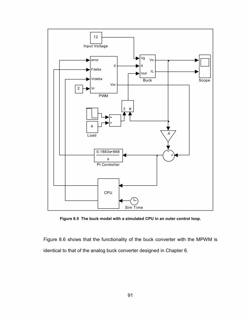
91
Sim Time
Scope
error
Fdelta
Vrdelta
Vr
d
Vor
PWM
0.1883s+868
s
PI Controller
4
Load
CPU
12
Input Voltage
.4
2
Vg
d
Iout
Vo
IL
Buck
Figure 8.5 The buck model with a simulated CPU in an outer control loop.
Figure 8.6 shows that the functionality of the buck converter with the MPWM is
identical to that of the analog buck converter designed in Chapter 6.

92
0 0.001 0.002 0.003 0.004 0.005 0.006 0.007 0.008 0.009 0.010
2
4
5
6
Voltage (
V)
Output Voltage of the Modified Buck Converter
0 0.001 0.002 0.003 0.004 0.005 0.006 0.007 0.008 0.009 0.010
10
20
30
Curr
ent
(A)
Time (sec)
Output Current of the Modified Buck Converter
Figure 8.6 Output voltage and current of the Modified Buck Converter.
The analog feedback was changed from TC to 0.45 (not shown). This change
represents a malfunction of the buck converter. As shown in Figure 8.7, this
change resulted in an increase of the DC output voltage of the buck converter to
about 5.5 V (shown before 1.5 msec), a 10% increase over the intended value of
5 V.
After 1.5 ms into the simulation, the CPU checked the output of the buck
converter and altered the reference for the MPWM in order to shift the buck
converter’s DC output back to the intended 5 V. Figure 8.6 shows the DC shift
from 5.5 V to 5 V at 1.5 ms.

93
0 0.5 1 1.5 2 2.5 3 3.5
x 104
0
1
2
3
4
5
6
7
Time (Sec)
Voltage (
V)
Figure 8.6 Analog control loop gain changed from 0.5 to 0.45.
Restoring the analog feedback gain to TC and arbitrarily changing the inductor
value from 15 µH to 3 µH the output ripple of the buck converter increased to
approximately 150 mV, shown in Figure 8.7 below. After 1.5 ms the CPU
checked the ripple magnitude and adjusted the switching frequency to alter the
output ripple to approximately 100 mV. The CPU also adjusted the DC offset
back to 5 V to maintain the output to the desired levels.
Before CPU adjustment
After CPU adjustment

94
1.48 1.5 1.52 1.54 1.56 1.58 1.6 1.62 1.64 1.66
x 104
4.92
4.94
4.96
4.98
5
5.02
5.04
5.06
5.08
5.1
Time (Sec)
Voltage (
V)
Figure 8.7 The ripple amplitude and DC output changed by the CPU.
Using the CPU to make adjustments in a Switched Mode Power Supply in the
above described method can add precision, robust operation, and user
interaction as in a digital power supply. It would limit the power wasted on
continuous processing, memory usage and control over a single system by
setting the appropriate output and conduct its power supply control algorithm in
set time intervals or as needed. Once the CPU determined the required
adjustments, it can set the output and not process anymore control algorithms
until it is scheduled to do so.
95
During the design and build phase of the power supply the designers and
builders would only need to design or build the SMPS to be within an output
range with much looser tolerances than they would otherwise need because the
CPU logic can correct the SMPS characteristics to provide the optimal SMPS
output once the unit is assembled, as in the digital power supply design. This
flexibility in the design and build phase of the SMPS could save companies
money and time to product output due component supply having the required
value tolerance levels.
For example, if a component manufacturer has a limited supply of inductors
whose value is 15 µH (see the original buck converter design above) the system
manufacturer could use a substitute inductor that would allow the system to start
within appropriate design margins, such as a 3 µH inductor from the MPWM
model simulation above, instead of waiting for specific component to become
available. Then once the system is started the CPU can adjust the reference
voltage and switching frequency to the ideal levels even though the ideal
component is not in use.

96
Chapter 9 Conclusion
Microcontrollers are replacing analog components within a classic SMPS to
produce the required pulse width modulated signal. These digital power supplies
provide advantages like the ability to enact advanced control schemes, robust
operation, and user interaction. However, due to the use of an active component
and memory a digital power supply may not have the power efficiency that a
passive analog design can provide.
Using the same design methods for analog SMPS, an intelligent SMPS can be
created by replacing the Pulse Width Modulator (PWM) in an SMPS with a
component that can enact commands from an intelligent source but not contain
the active components, such as a processor, a power supply can gain the
benefits of intelligent control and the benefits of a power efficient design by
allowing the Central Processing Unit (CPU) in the computer system to receive
feedback information from the power supply and make decisions on any needed
adjustments within the power supply. At power on or start-up of the CPU this
modified PWM regulates the output of the power supply based on an analog
control scheme. After the CPU is started it begins making adjustments to the
power supply to obtain the most efficient and effective output.
In this manner, a power design can be sent to production sooner due to fewer
design and testing iterations to find the exact component values to produce the

97
correct output voltage and ripple. A power supply design would only need to
produce an output that is within the operational limit of the dependant system
until the CPU made adjustments to improve the performance of the power
supply.

98
Appendix A SG1526 PWM Datasheet

99
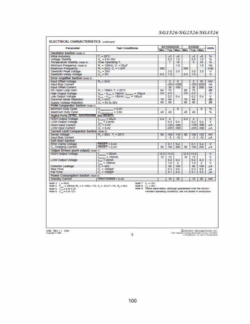
100

101

102

103

104

105

106

107
Appendix B DSCC MIL-PRF-39006/22H, Table
I
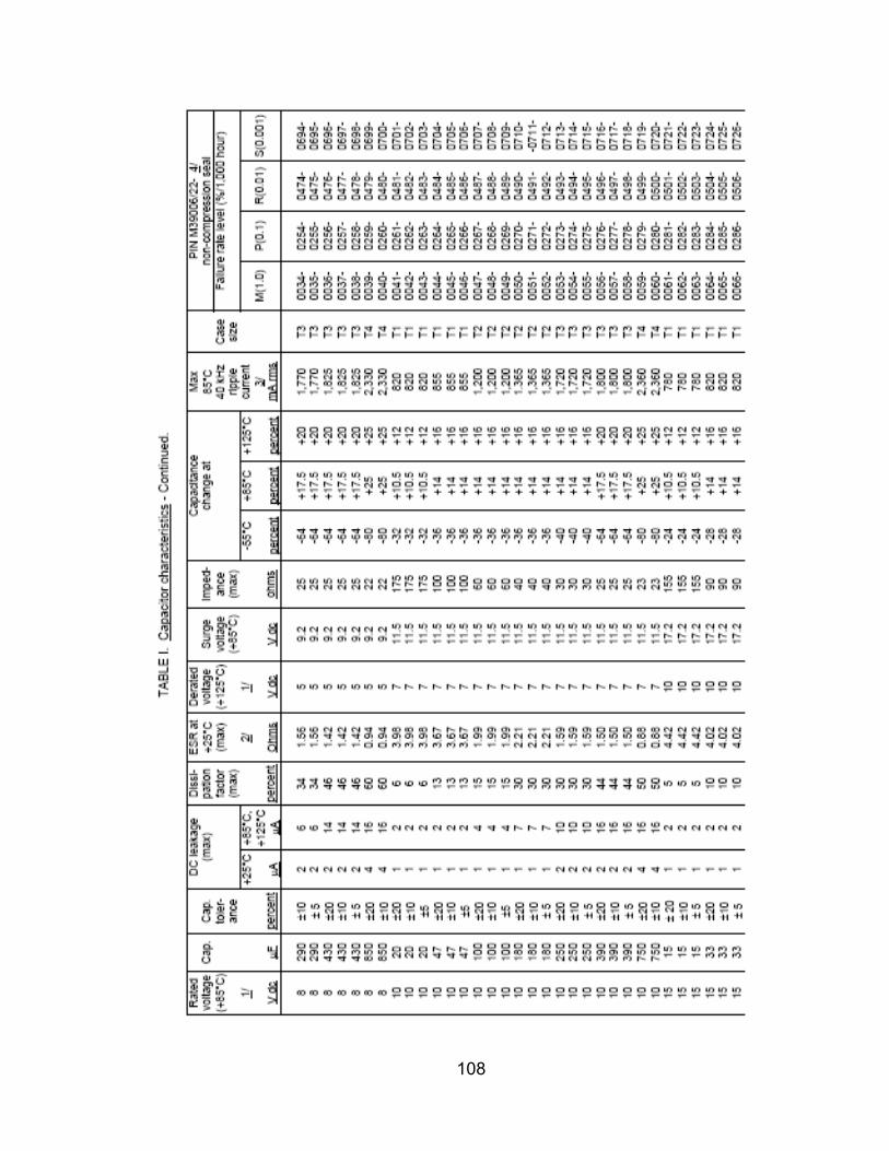
108
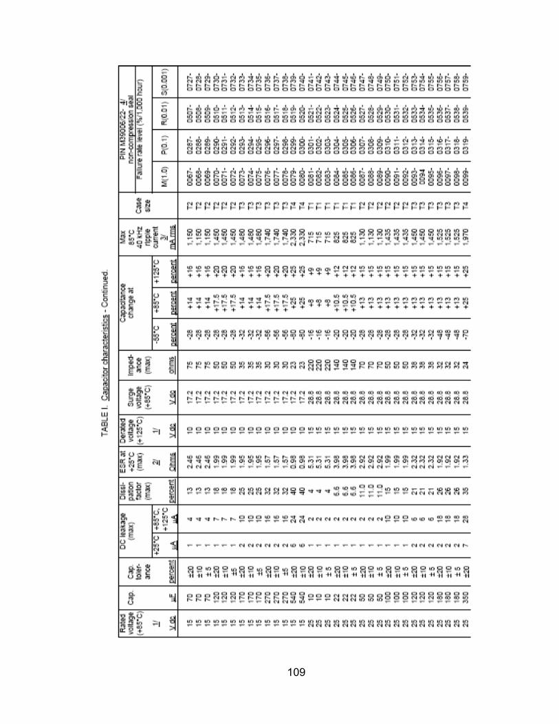
109
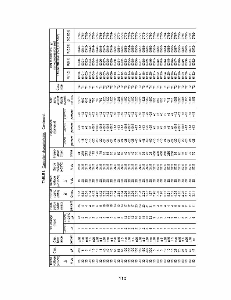
110
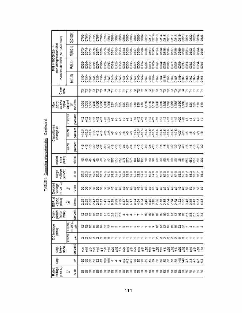
111
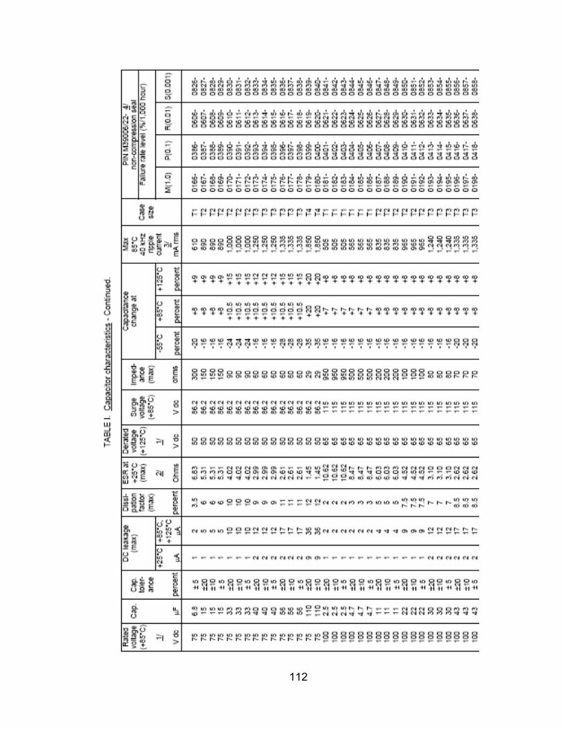
112

113

114
Appendix C DSCC MIL-PRF-39014/22E Table III

115

116

117

118

119
Appendix D DSCC MIL-PRF-39003/10C CSS13 Table I

120

121

122

123
References
[1] M. K. Kazimierczuk, Pulse-Width Modulated DC-DC Power Converters.
John Wiley & Sons Ltd, 2008.
[2] R. A. Mack Jr., Demystifying Switching Power Supplies. Elsevier Inc,
2005.
[3] R. J. Beichner and R. A. Serway, Physics: For Scientists and Engineers.
Saunders College Publishing, 2000.
[4] J. Ken, “’Shoot-Through in Synchronous Buck Converters”. Fairchild
Semiconductor, 2003
[5] M. Tarr, “Electrolytic Capacitors”. http://www.ami.ac.uk/courses/
topics/0136_ec/, 2003.
[6] Kuo & Golnaraghi, Automatic Control Systems.
John Wiley & Sons Ltd, 2003.
[7] Liu, Yan-Fei & Sen, P.C., “Digital Control of Switching Power Converters”.
IEEE Conference on Control Applications, 2005.

124
[8] Simone, Buso, & Mattavelli, Paolo Digital Control in Power Electronics.
Morgan & Claypool Publishers, 2006.
[9] Phillips, Charles L. & Nagle, H. Troy Digital Control System Analysis and
Design. Prentice-Hall Inc, 1995.