novel control of a permanent magnet linear generator for ocean
TRANSCRIPT


AN ABSTRACT OF THE THESIS OF
Aaron H. VanderMeulen for the degree of Master of Science in Electrical Engineering presented on June 14, 2007. Title: Novel Control of a Permanent Magnet Linear Generator for Ocean Wave Energy Applications.
Abstract approved: _____________________________________________________
Ted Brekken
_____________________________________________________
Annette von Jouanne
Wave energy conversion devices are a rapidly growing interest worldwide for
the potential to harness a sustainable and renewable energy source. Due to the
oscillatory nature of ocean waves, the power generated from a permanent magnet
linear generator (PMLG) for ocean wave energy conversion is pulsed. Focusing on
direct drive technology, the PMLG directly translates the motion of the waves into
electrical energy. The power generated, left unconditioned, is not easily used or stored.
With conventional diode rectification topologies, line currents can not be
controlled easily, resulting in an uncontrolled generator output and force. With an
active rectifier topology, the real and reactive power from the PMLG is fully
controllable. This thesis will investigate the generator modeling and design of a novel
three-phase active rectifier topology and force controller with a dc-dc converter for
bus voltage regulation. An in depth analysis for the controller design and simulations
are presented. Hardware for the three-phase active rectifier is specified and built with
initial lab test results. The controller design is implemented with National Instruments’
LabView and compiled on a CompactRIO real-time controller.

©Copyright by Aaron H. VanderMeulen June 14, 2007
All Rights Reserved

Novel Control of a Permanent Magnet Linear Generator for Ocean Wave Energy Applications
by Aaron H. VanderMeulen
A THESIS
submitted to
Oregon State University
in partial fulfillment of the requirements for the
degree of
Master of Science
Presented June 14, 2007 Commencement June 2008

Master of Science thesis of Aaron H. VanderMeulen presented on June 14, 2007 APPROVED: Major Professor, representing Electrical and Computer Engineering Co-Major Professor, representing Electrical and Computer Engineering Director of the School of Electrical Engineering and Computer Science Dean of the Graduate School I understand that my thesis will become part of the permanent collection of Oregon State University libraries. My signature below authorizes release of my thesis to any reader upon request.
Aaron H. VanderMeulen, Author

ACKNOWLEDGEMENTS
I would like to thank my major professor, Dr. Ted Brekken for his guidance,
enthusiasm and sincerity during my experience with the Energy Systems Group. I
would also like to thank my co-major professor Dr. Annette von Jouanne for her
support, guidance and passion with my research and time with the Energy Systems
Group. Special thanks go to the late Dr. Alan Wallace. His passion and knowledge are
greatly missed and will always be remembered.
Thanks go to my committee members: Dr. Jimmy Eggerton and Dr. Joe
Zaworski for their time and efforts. For their knowledgeable advice, support of my
research and ongoing friendship I would like to thank Ean Amon, Peter Hogan, Al
Schacher, Ken Rhinefrank and other members of the Energy Systems Group.
Finally, my biggest thanks go to my parents, Fred and Yun, and sister, Cindy,
for their enduring love, support, and encouragement through my academic studies and
my life; you have shaped my life and I would not have been able to do this without
you.

TABLE OF CONTENTS
Page
1 INTRODUCTION ......................................................................................................1
1.1 Background ..........................................................................................................1
1.2 Wave Energy........................................................................................................1
1.3 Power Electronics.................................................................................................6
2 GENERATOR MODELING.......................................................................................8
2.1 Ideal Model ..........................................................................................................8
2.2 Dynamic .............................................................................................................12
3 PASSIVE RECTIFIER INVESTIGATIONS............................................................17
3.1 Passive Rectifier Overview................................................................................17
3.2 Passive Rectifier Simulations.............................................................................17
3.3 Ideal Source with Passive Rectifier....................................................................19
3.4 Summary of Passive Rectifier Results ...............................................................36
4 DQ CONTROL..........................................................................................................39
4.1 dq Overview.......................................................................................................39
4.2 Transfer Function of Generator..........................................................................42
4.3 Controller Design ...............................................................................................45
4.4 Controller Verification.......................................................................................54
5 THREE-PHASE SYNCHRONOUS ACTIVE RECTIFIER.....................................57
5.1 Active Rectifier Overview .................................................................................57
5.2 Ideal Wave Model Simulations..........................................................................57
5.2.1 Switching Model ........................................................................................58

TABLE OF CONTENTS (Continued)
Page
5.2.2 Average Model ...........................................................................................64
5.3 Dynamic Model Simulations .............................................................................70
5.4 Stochastic Wave Simulations.............................................................................74
6 GATING SIGNAL GENERATION
6.1 Pulse Width Modulation ....................................................................................79
6.2 Sine-Triangle PWM ...........................................................................................79
7 DC/DC CONVERTER ..............................................................................................82
7.1 Mathematical Model ..........................................................................................83
7.1.1 Boost Circuit ..............................................................................................83
7.1.2 Buck Circuit ...............................................................................................86
7.2 Resistive Loading...............................................................................................86
7.3 Hysteretic Control ..............................................................................................87
8 POWER TAKE OFF FROM BUOY.........................................................................89
8.1 Testing Configurations.......................................................................................89
8.2 Marine Cables ....................................................................................................90
8.3 Control of Power Electronics .............................................................................91
9 HARDWARE IMPLEMENATION ..........................................................................93
9.1 Hardware Selection ............................................................................................93
9.2 Passive Rectifier Testing..................................................................................101
9.3 Active Rectifier Testing ...................................................................................108

TABLE OF CONTENTS (Continued)
Page
10 CONCLUSION......................................................................................................112
Bibliography ...............................................................................................................114

LIST OF FIGURES
Figure Page
1.1 Average wave period .....................................................................................................3
1.2 Significant wave height..................................................................................................3
1.3 Progressive surface wave parameters ............................................................................4
1.4 Surface particle velocity ................................................................................................5
2.1 PMLG cross-sectional area ............................................................................................9
2.2 Ideal wave mathematical model...................................................................................11
2.3 Per-phase voltage to SimPowerSystem Block interface..............................................11
2.4 Dynamic generator/buoy model...................................................................................14
2.5 PMLG dynamic Simulink model .................................................................................16
3.1 Diode reverse recovery charge.....................................................................................17
3.2 Simulink passive rectifier model .................................................................................19
3.3(a) Rectifier input voltage (no dc bus capacitance) ......................................................20
3.3(b) Generator back EMF (no dc bus capacitance) ........................................................20
3.3(c) Rectifier input voltage (zoom).................................................................................21
3.3(d) Line current (no dc bus capacitance).......................................................................22
3.3(e) Line current (zoom).................................................................................................23
3.3(f) dc bus voltage ..........................................................................................................24
3.3(g) Peak dc bus voltage.................................................................................................25
3.3(h) dc bus current ..........................................................................................................25

LIST OF FIGURES (Continued)
Figure Page
3.3(i) Peak dc bus current ..................................................................................................26
3.4(a) Generator back EMF ...............................................................................................28
3.4(b) Rectifier input voltage.............................................................................................28
3.4(c) Rectifier input voltage (zoom).................................................................................29
3.4(d) Line current .............................................................................................................30
3.4(e) Line current (zoom).................................................................................................30
3.4(f) dc bus voltage ..........................................................................................................31
3.4(g) dc load current.........................................................................................................31
3.5(a) Generator back EMF ...............................................................................................32
3.5(b) Rectifier input voltage.............................................................................................33
3.5(c) Input line current .....................................................................................................33
3.5(d) Input line current (zoom).........................................................................................34
3.5(e) Rectifier dc bus voltage ...........................................................................................35
3.5(f) Rectifier dc bus current ............................................................................................35
3.6 Three-phase diode bridge rectifier ...............................................................................37
4.1 Three-phase to two-phase projection ...........................................................................39
4.2 Per-phase equivalent circuit .........................................................................................42
4.3 Control toplogy ............................................................................................................45
4.4 Plant transfer function..................................................................................................48
4.5 Bode plot of plant and controller open loop transfer function.....................................49

LIST OF FIGURES (Continued)
Figure Page
4.6 Controller crossover frequency, phase and gain margin..............................................50
4.7 Loop gain control topology..........................................................................................52
4.8 Average model .............................................................................................................52
4.8 Three-phase active rectifier equivalent circuit.............................................................52
4.10 Controller layout ........................................................................................................53
4.11 Simulink controller layout .........................................................................................53
4.12 Average model in Simulink .......................................................................................54
4.13 Step response of closed-loop controller and plant .....................................................55
5.1 Three-phase active rectifier with dc bus regulator.......................................................58
5.2 dq-control Simulink model ..........................................................................................58
5.3(a) Active rectifier input voltage (280VLLrms) ...............................................................59
5.3(b) Generator back EMF (280VLLrms) ...........................................................................60
5.3(c) Line input current (280VLLrms) ................................................................................60
5.3(d) dc bus voltage..........................................................................................................61
5.3(e) dc bus current into capacitor....................................................................................62
5.3(f) Isq measured vs. reference ........................................................................................63
5.3(g) Isd measured vs. referencee......................................................................................63
5.4(a) Isdq current output ....................................................................................................64
5.4(b) Isq actual vs. reference .............................................................................................65
5.4(c) Isd actual vs. reference .............................................................................................66

LIST OF FIGURES (Continued)
Figure Page
5.9(a) Generator output voltage .........................................................................................67
5.9(b) Active rectifier input voltage...................................................................................67
5.9(c) Active rectifier input current ...................................................................................68
5.9(d) Sinusoidal Isq current output....................................................................................69
5.9(e) Isd actual vs. reference .............................................................................................69
5.9(f) Isq actual vs. reference..............................................................................................70
5.10 Dynamic PMLG and controller Simulink model.......................................................71
5.11(a) Isq current measured vs. reference .........................................................................71
5.11(b) Isd current measured vs. reference .........................................................................72
5.11(c) Rectifier applied output voltage ............................................................................73
5.11(d) Isq current measured vs. reference .........................................................................73
5.11(e) Isd current measured vs. reference ........................................................................74
5.12 Force input block .......................................................................................................75
5.13(a) Stochastic sea state ................................................................................................75
5.13(b) Generated prescribed force reference and measured.............................................76
5.13(c) Commanded current reference and measured .......................................................77
5.13(d) Average rectifier applied voltage ..........................................................................77
6.1 Three-phase IGBT bridge ............................................................................................79
6.2 PWM generator with dead-time...................................................................................80
7.1 Test system setup .........................................................................................................82

LIST OF FIGURES (Continued)
Figure Page
7.2 Future test setup ...........................................................................................................82
7.3 Boost circuit layout ......................................................................................................83
7.4 Buck circuit layout ......................................................................................................84
7.5 Simulink dc converter model .......................................................................................87
7.6 Hysteretic controller for dc converter ..........................................................................88
8.1 Marine cables from the AmerCable Inc. brochure.......................................................90
8.2 cRIO NI-9012 RT controller........................................................................................91
8.3 NI-9205 analog input module ......................................................................................92
8.4 NI-9474 digital output module.....................................................................................92
9.1 PowerEx Pow-R-Pak PP75T120 assembly..................................................................96
9.2(a) 4 IGBT modules mounted on heat-sink...................................................................98
9.2(b) Assembled three-phase active rectifier with driver board.......................................98
9.2(c) Reverse side of the three-phase active rectifier .......................................................99
9.2(d) dc bus capacitor (1100uF, 1350V) ........................................................................100
9.2(e) Programmable source ............................................................................................101
9.3(a) Variable-voltage rectifier input (161VLLpk)...........................................................102
9.3(b) Line input current (161VLLpk) ...............................................................................103
9.3(c) DC bus current (161VLLpk) ....................................................................................103
9.3(d) DC bus voltage (161VLLpk) ...................................................................................104
9.3(e) Phase-a voltage and current (161VLLpk) ................................................................104

LIST OF FIGURES (Continued)
Figure Page
9.4(a) Variable-voltage rectifier input (161VLLpk and dc capacitance 1100uF) ..............105
9.4(b) Line input current (161VLLpk and dc capacitance 1100uF) ...................................105
9.4(c) Line input current (zoom) (161VLLpk and dc capacitance 1100uF).......................106
9.4(d) Phase-a voltage and current (161VLLpk and dc capacitance 1100uF)....................106
9.4(e) dc bus capacitor voltage and current (161VLLpk and dc capacitance 1100uF) ......107
9.4(f) dc bus capacitor voltage (161VLLpk and dc capacitance 1100uF)..........................107
9.4(g) dc load current (161VLLpk and dc capacitance 1100uF)........................................108
9.5(a) Three-phase to dq-reference frame........................................................................109
9.5(b) dq-reference frame to three-phase.........................................................................109
9.5(c) Pulse Width Modulated gating signal generator ...................................................110
9.5(d) PI controller...........................................................................................................110

LIST OF TABLES
Table Page
1.1 Peak velocity at 1.5m wave height ................................................................................6
1.2 Peak velocity at 3.0m wave height ................................................................................6
3.1 Wave height and linear velocity ..................................................................................37
3.2 dc bus resistve loads.....................................................................................................37
3.3 Passive rectifier simulation results...............................................................................38
9.1 Summary of passive rectifier testing (hardware).......................................................108

Novel Control of a Permanent Magnet Linear Generator for Ocean Wave Energy Applications
1 INTRODUCTION
1.1 Background
Wave energy conversion devices are a rapidly growing interest worldwide for the
potential to harness a sustainable, predictable and almost unlimited energy resource.
Water has a much higher density than that of air thus the dimension of the energy
converting device takes up less space compared to that of wind turbines. Wave energy
is a form of concentrated solar power originating from the uneven heating of the earth
creating wind and wind in turn creating waves. The waves gather energy across vast
stretches of ocean resulting in high power energy sources near coastal shores. The
wave energy system presented utilizes the heave (vertical) motion of the wave.
Therefore the output power will be modulated at the wave frequency, approximately 5
to 10 seconds. This pulsed power needs to be conditioned and regulated for connection
to a utility grid. Advancements in power electronics technology has made wave energy
power production possible with maximum efficiency and maximum power extraction
from the wave.
1.2 Wave Energy
Ocean energy conversion encompasses ocean waves, ocean tides and ocean
currents as a source to extract electrical energy. There are various mechanical devices
currently deployed that convert ocean waves into electrical energy. Such devices
include Ocean Power Delivery’s Pelamis Wave Energy Converter and Ocean Power
Technology’s PowerBuoy. These devices translate ocean wave motion into electrical
energy mechanically via a hydraulic system to a rotary generator. This added
intermediary step of mechanical components adds to system losses and maintenance
with increased moving parts. At Oregon State University, the Energy Systems group is

2
focusing on wave energy converters that eliminates the mechanical linear to rotary
conversion altogether. This thesis primarily focuses on direct drive technology
employing linear electric machines.
Ocean wave devices translate kinetic motion into linear motion from the wave
excitation force. This force moves the buoy float vertically along the spar, creating the
relative motion between generator components in the heaving float vs. the stationary
spar. The spar is moored to the sea floor, making it relatively stationary.
The excitation force will move the float linearly with a velocity. The relative
motion between the permanent magnets and the coils will generate the electrical
energy. Faraday’s law explains how a change in a magnetic field relative to a coil will
induce a voltage within the coil. The relative motion of the permanent magnets
relative to the coils in a direct drive linear generator is the basis on which electrical
energy is created. Len’s law describes the magnetic field produced by the coils acting
in the opposite direction of the changing magnetic field which produced it. This
creates a constant magnetic flux within the active region and produces an opposing
generator force. For the direct drive linear generator, such devices are built to generate
high voltages to reduce the amount of current drawn through the coils.
Ocean waves have varying wave periods and height determined by winds and the
distance traversed. The height of a wave is defined by the distance from the crest
(peak) to the trough (low point). The period of the wave is determined by the distance
from crest to crest. Data collected off of the Oregon Coast by NOAA (National
Oceanographic and Atmospheric Association) buoys show a trend seen in figures 1.1
and 1.2.

3
Fig. 1.1 – Average wave period
Fig. 1.2 - Significant wave height

4
For computer simulations of the generator (generator and buoy system) interface
with the power electronics, vertical velocities will be varied in order to generate
different voltage levels. The maximum vertical velocity will determine the maximum
output voltage and thus the power electronics will need to be designed to handle this
output voltage.
Fig. 1.3 - Progressive surface wave parameters
Figure 1.3 shows the progressive surface wave parameters for a monochromatic
wave traveling at a phase celerity (phase velocity), C. Other defining parameters are
the wave height, H, in meters, wave length, L, in meters, and wave depth, d, in meters.
The wave velocity is defined by the wave length, L, and wave period, T. [1]
T
LC = (1.1)
As the wave front travels from left to right, the motion of the particles are shown by
the arrows in figure 1.3. The orbiting dimensions decrease to zero as depth increases.
At the surface a water particle will experience an upward vertical velocity from the
incoming wave front. The velocity is represented by equation 1.1. The generator will
be considered a particle on the surface of the wave, where z = 0 and any damping or
5
phase shifting is neglected. Therefore, the generator will be considered to be a wave
follower. The vertical velocity of a particle is shown in equation 1.2.
( )tkxeT
Hw kz
s σπ −= sin (1.2)
Lk
π2= (1.3)
T
πσ 2= (1.4)
Equation 1.3 is the wave number and equation 1.4 is the wave angular frequency.
For investigation, the maximum velocity of the generator will be at position z = 0. The
vertical velocity is then reduced to:
( )tkxT
Hwc σπ −= sin (1.5)
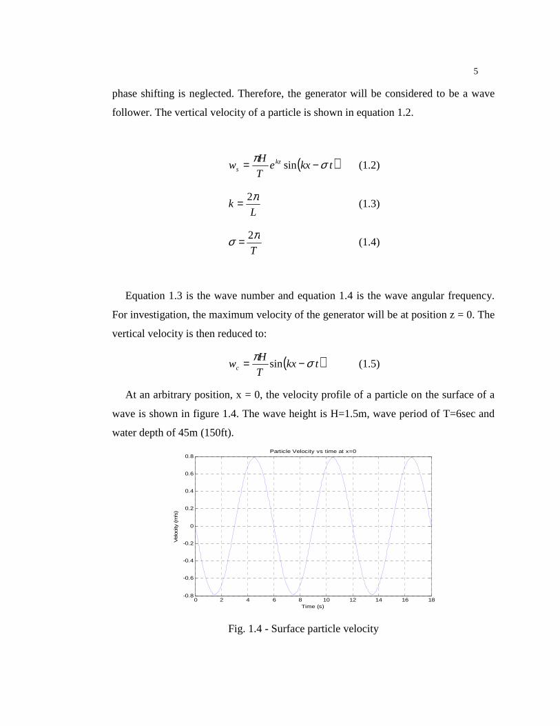
At an arbitrary position, x = 0, the velocity profile of a particle on the surface of a
wave is shown in figure 1.4. The wave height is H=1.5m, wave period of T=6sec and
water depth of 45m (150ft).
0 2 4 6 8 10 12 14 16 18-0.8
-0.6
-0.4
-0.2
0
0.2
0.4
0.6
0.8Particle Velocity vs time at x=0
Time (s)
Vel
ocity
(m
/s)
Fig. 1.4 - Surface particle velocity

6
For our investigations, H ranges from 1m to 3m. Keep in mind that the maximum
buoy travel for the 1kW generator is 1m, but the velocity of the buoy will change with
wave height. The wave length will be fixed at 91 meters, the average wave length. For
ideal monochromatic wave generation, the wave period will be varied to generate a
range of output voltages from the generator. The reason for varying the wave period is
explained in the ideal wave generator model section.
The peak linear velocity can be found using wave height, Ho, and wave period To,
using equation 1.6.
o
oc T
Hw
π= (1.6)
Wave Period (s) Wave Height (m) Velocity (m/s) 6 1.5 0.785 8 1.5 0.589 10 1.5 0.471
Table 1.1 – Peak velocity at 1.5m wave height
Wave Period (s) Wave Height (m) Velocity (m/s) 6 3.0 1.571 8 3.0 1.178 10 3.0 0.942
Table 1.2 – Peak velocity at 3.0m wave height
1.3 Power Electronics
The field of power electronics has rapidly expanded allowing for the construction
of new devices that were not possible even a decade ago. New materials and
production methods have allowed for higher switching frequencies, increased current,
high voltage, and higher power capabilities. High powered IGBTs (Insulated Gate

7
Bipolar Transistors) now have faster switching frequencies which makes them
competitive with fast-switching FET (Field Effect Transistor) devices. However, the
FET devices do not allow the higher power handling capabilities of the IGBT; the
IGBT still is ideal in higher power switching topologies.
With different active rectifier front-end topologies, it is possible to control the
real and reactive power flow in and out of a generator. The generator variable voltage
variable frequency output is not readily usable since the power output is pulsed due to
the low frequency excitation force. For example, if an incandescent light bulb is
placed on the terminals, it would flash on and off with twice the electrical frequency
output of the generator. The power electronics described in this thesis will interface
between the generator terminals and a dc-dc converter. The dc-link will provide a stiff
bus voltage, temporary energy storage and an interface to a loading system.

8
2 GENERATOR MODELING
The generator model will interface with the power electronics and controls
components for ideal and dynamic system simulations. The ideal wave model will
interface with the SimPowerSystems blocks in MATLAB/Simulink as well as the
average model of the power electronics. The dynamic generator model will interface
with the average switching model of the power electronics and the stochastic wave
environment.
2.1 Ideal Model
The permanent magnet linear generator (PMLG) is designed for a maximum of 1
meter vertical displacement, limited by the active magnetic region, and a speed range
from 0 to 3 m/s. These parameters are used in the construction of a
MATLAB/Simulink ideal wave source model used to test all power electronic
topologies. The ideal source produces a monochromatic wave used as a baseline. The
monochromatic wave output only represents a single wave envelope frequency versus
a stochastic ocean wave environment where many harmonic frequencies exist. The
monochromatic wave output is considered for understanding of the generator. The
ideal wave model input variables required are changes in wave period and changes in
output voltages.
The ideal source is derived mathematically based on magnetic and electrical
properties, as well as wave mechanics. Vertical displacement of the generator depends
on the maximum range associated with a specific generator, d in equation 2.1. The
maximum distance traveled for the PMLG in consideration is 1m. The generator will
be displaced vertically due to the wave excitation force. This force in ideal conditions
is sinusoidal. The vertical displacement, y(t), is shown in equation 2.2, where mω is

9
the ocean wave frequency in rad/sec and the maximum generator travel, d, in meters.
[2]
mmm
m
Tf
td
ty
ππω
ω
2*2
)sin(2
)(
==
= (2.1)
The flux seen by the coils within the spar, respect to time (zero initial conditions) is
shown in equation 2.2. The variable Φ is the peak flux produced by the permanent
magnets in Tesla and λ is the magnetic wavelength in meters. The pole pitch for the
linear generator is half of the magnetic wavelength.
Φ=∧
)(*2
sin*)( tytλπφ (2.2)
Fig. 2.1 - PMLG Cross-sectional area.
The voltage induced in the coils can be described by Faraday’s Law by equation
2.3, where N is the number of turns per coil, and the change in flux. Differentiating the
flux associated with time, equation 2.4, results in the per-phase voltage. ∧V is the peak
phase-to-neutral voltage. Since the linear generator is a three-phase machine, each
phase is electrically phase shifted 120 degrees, shown in equation 2.4 and 2.5.

10
dt
dNtv
φ=)( (2.3)
( ) ( )
3
2/,0
sincoscos)(
πϑ
ϑωλ
πω
−+=
+=∧
td
tVtv mm
(2.4)
( ) ( )
( ) ( )
( ) ( )
+=
−=
=
∧
∧
∧
3
2sincoscos)(
3
2sincoscos)(
sincoscos)(
πωλ
πω
πωλ
πω
ωλ
πω
td
tVtv
td
tVtv
td
tVtv
mmc
mmb
mma
(2.5)
The peak electrical frequency is calculated by dividing the peak speed of the
translator by the magnetic wavelength. Equation 2.6 shows the peak electrical
frequency calculation where d is in meters and magnetic wavelength λ is in meters.
The peak electrical frequency associated with equation 2.6 is expected because the
magnetic wavelength represents a complete cycle from north to south. By increasing
the velocity of this transition, the cycle time decreases.
λ
λπω
pke
e
velocityf
dt
dx
=
=
ˆ
2ˆ
max (2.6)
The ideal wave source was assembled in Simulink with the corresponding
parameters, where the ocean wave frequency,mω , is the variable:

11
( )mm f
mmm
md
πωλ
2
144.0144
1
===
=
Fig. 2.3 – Ideal wave mathematical model
Fig. 2.4 – Per-phase voltage to SimPowerSystem Block interface
Figure 2.4 shows the monochromatic wave model interfaced with the
SimPowerSystems dependent voltage source blocks. SimPowerSystems is an add-on
to Simulink that allows circuits to be simulated. The SimPowerSystems blocks are
used to output a voltage dependent on the input reference. The SimPowerSystems
blocks are similar to circuit simulation layout, where node voltages and currents can
be easily measured.

12
2.2 Dynamic Model
A dynamic generator model will allow faster simulation performance times since
the switching model can be verified using an average model. With the ideal generator
model, it is easy to select some desired current reference based on the output voltage
from the generator; however there is no feedback to the generator system. By
developing a dynamic linear generator model, verification that the switching control
works in conjunction with it will transition into a full hardware based test.
The dynamic linear generator equations are similar to those of a rotary permanent
magnet synchronous generator that were used to develop the control system. The
equations however differ slightly because of the torque and force representation. The
rotational mechanical angle in a rotary machine is dependent upon the angular
velocity, whereas the mechanical ‘angle’ of the linear generator is dependent upon the
linear velocity.
The dq-axis equations for a linear generator are presented below, where Rs is the
coil resistance, mω is the electrical angular frequency, iq is the q-axis current, id is the
d-axis current and fdλ is the excitation linkage flux of the stator due to flux produced
by the magnets. Also, Vd is the d-axis voltage and Vq is the q-axis voltage. [3]
sdmsqsqssq
sqmsdsdssd
dt
diRv
dt
diRv
λωλ
λωλ
++=
−+= (2.7)
mlss
sqssq
fdsdssd
LLL
iL
iL
+=
=
+=
λλλ
(2.8)

13
Combining both parts of equation 2.7 and 2.8, results in the cross coupled dq-
voltage equations.
( )
sdssqssqssq
sqsmfdsdssdssd
iLiLdt
diRv
iLiLdt
diRv
ω
ωλ
++=
−++= (2.9)
mechm
p ωω2
= (2.10)
In equation 2.11, the rotational mechanical frequency relates to the electrical
frequency, both in rad/sec, by the number of poles of the machine.
( )sdsqsqsdem iip
T λλ −=2
(2.11)
Substituting in the dq-flux linkage from equation 2.8, results in equation 2.12
giving the output torque related to the q-axis current and magnet excitation flux
linkage.
( )( ) sqfdsdsqssqfdsdsem ip
iiLiiLp
T λλ22
=−+= (2.12)

14
Fig. 2.5 – Dynamic generator/buoy Model
The dynamic system layout is shown in figure 2.5. The hydrodynamic model and
dynamics model will generate forces created by an ocean wave. Optimal Force
Controller block will intelligently compute the optimal generator loading. The wave
excitation force will exert a force upon the buoy and the generator will prescribe a
force to exert upon the wave. This generator force is determined by the current output
of the generator.
The q-axis current substituted into equation 2.11, resulting in torque. The torque is
force times the radius of a machine. Equation 2.13 expresses the length of the stator
for a linear generator is the pole pitch,τ , times the number of poles, p. The
circumference of a rotary synchronous generator is expressed in equation 2.13, where
r is the mean radius of the rotor. [6]
pphasespl ττ 3== (2.13)
rc π2= (2.14)

15
Substituting in equation 2.13 into equation 2.14 where the length and
circumference are equal:
πτ2
3 pr = (2.15)
Assuming a 2 pole machine, 1 pole pair, the radius of a machine is equal to:
πτ3=r (2.16)
For a rotary machine with 2 poles, the torque output is equal to:
sqfdem iT λ= (2.17)
The torque is equal to force times radius thus relating torque and force, results in:
sqfdem ir
TF λ
τπ3
== (2.18)
The force output of a linear synchronous machine of multiple pole pairs will
increase linearly with the number of pole pairs, like a rotary machine the poles pairs
will linearly increase the torque. A general equation for force output is equation 2.19:
sqfd ip
F λτπ
6= (2.19)

16
The Simulink model for the permanent magnet linear machine is shown in figure
2.6.
Fig. 2.6 – PMLG dynamic Simulink model
The force output is computed from a measured Iq current, this force is then fed back
into the Optimal Force Controller. The force block, labeled ‘f(u)’ is shown in figure
2.6 after the ‘Lambda_dqidq’ block

17
3 PASSIVE RECTIFIER INVESTIGATIONS
3.1 Passive Rectifier Overview
Line commutated passive rectifiers in this investigation will be used as a reference
with which three-phase active rectifier results will be compared. The passive rectifier
operation is based on the line-to-line voltage and the dc-bus voltage. The diode
rectification investigation is vital knowledge, since in the event of switching failure of
an active rectifier, the buoy will still generate power in this manner and thus the
electronics will need to be designed to handle such events.
3.2 Passive Rectifier Simulations
For the passive rectifier simulations, a model was built using MATLAB/Simulink
with models from the SimPowerSystems Library. The passive rectifier was arranged
in a three-phase six-pulse full-bridge topology. The diodes each have snubber circuits
utilizing a series capacitor and resistor to reduce high voltage spikes during switching
modes which can cause the diodes to fail. The di/dt time can be calculated using
equation 3.1. [4]
Fig. 3.1 - Diode reverse recovery charge

18
σL
V
dt
di d−= (3.1)
Equation 3.1 relates the change in current with the voltage and inductance
connected to the device. A curve similar to figure 3.1 shows what visually happens
when current is quickly switched. Vd is the voltage across the device, the worst case
scenario for a diode bridge is with zero dc bus voltage and full input voltage. The
voltage Vd is selected as the maximum output voltage per phase. The peak phase
voltage at velocity 2m/s is 655VLN. The inductance is dominated by the source
inductance of the permanent magnet linear generator, thus stray inductances are
neglected. [5]
sAmH
V
dt
di23625
24*2
1134 −=−= (3.2)
rrrr tdt
diI
= (3.3)
The reverse recovery current, Irr, can be defined by equation 3.3 above where the
reverse recovery time is trr. The reverse recovery time specification is available on
most IGBT/diode packages. For the IGBT/module CM75DU-24F, the reverse
recovery time measured under inductive load testing at full rated current and dc bus
voltage is 150ns. Using this time required in equation 3.3, the maximum reverse
recovery current is Irr = -3.54mA. The snubber capacitance is defined by equation 3.4
below, where Ls is source inductance and VLL is the line-to-line RMS voltage.
2
=
LL
rrss V
ILC (3.4)

19
Since the source inductance, the line-to-line voltage, and the reverse recovery
current are all known, the computed snubber capacitance can be calculated as Cs =
2.34e-13F. The required snubber resistance is then found with equation 3.5.
rr
LLpeaks I
VR 3.1= (3.5)
Using 1134V, the peak line-to-line voltage produced by the generator at 2m/s, and
the previously computed reverse recovery current, the snubber resistance if found to
be 416 Ωk .
3.2 Ideal Source with Passive Rectifier
Fig. 3.2 – Simulink Passive Rectifier Model
The three-phase diode bridge is shown in figure 3.2. Each diode has a turn-on
voltage of 3V and a turn-on resistance of 1Ωm . Each diode has a parallel RC snubber

20
circuit with values calculated previously. The dc load resistance is 156Ω to produce
peak 1kW. The wave period is T=6s and voltage levels for 0.7m/s velocity.
Voltage Input: VLLrms = 280V, VLNpk = 228V (0.7m/s)
0 1 2 3 4 5 6-250
-200
-150
-100
-50
0
50
100
150
200
250Voltage Input
Time (Sec)
Vol
tage
(V)
Phase A - Voltage
Phase B - VoltagePhase C - Voltage
Fig. 3.3(a) – Rectifier input voltage (no dc bus capacitance)
0 1 2 3 4 5 6-250
-200
-150
-100
-50
0
50
100
150
200
250Generator Back EMF
Time (Sec)
Vol
tage
(V)
Phase A - Voltage
Phase B - VoltagePhase C - Voltage
Fig. 3.3(b) – Generator back EMF (no dc bus capacitance)

21
Figure 3.3(a) shows the input voltage; the peak line-to-neutral voltage is 228V with
the eight pulses on the upstroke and eight pulses on the down-stroke. The generator
back EMF has a slightly higher voltage due to the drop across the line resistance and
source inductance. The current draw at peak voltages results in the notches seen in
figure 3.3(c).
2.85 2.9 2.95 3 3.05 3.1 3.15-300
-200
-100
0
100
200
300
X: 2.863Y: 225
Voltage Input
Time (Sec)
Vol
tage
(V)
X: 3.14Y: 224.9
Phase A - Voltage
Phase B - VoltagePhase C - Voltage
Fig. 3.3(c) – Rectifier input voltage (zoom)
Figure 3.3(c) shows the time when the peak electrical frequency occurs. The
electrical frequency calculated is:
Hzsstt
8.3883.214.3
11
12
=−
=−
This electrical frequency is less than the anticipated 5.5Hz. This is due to
limitations of the source model used. The model has a maximum travel of 1m. This
results in having only a 1 meter wave height, when this is not the case. The limitations

22
of the model for the stroke length result in off peak electrical frequencies. The peak
electrical voltages, however, are correct.
0 1 2 3 4 5 6-3
-2
-1
0
1
2
3Generator Output Current
Time (Sec)
Cur
rent
(A)
Phase A - Current
Phase B - CurrentPhase C - Current
Fig. 3.3(d) – Line current (no dc bus capacitance)
Peak current levels are shown in figure 3.3(d) and (e) at approximately 2.5A.

23
2.85 2.9 2.95 3 3.05 3.1 3.15-3
-2
-1
0
1
2
3Generator Output Current
Time (Sec)
Cur
rent
(A)
Phase A - Current
Phase B - CurrentPhase C - Current
Fig. 3.3(e) – Line current (zoom)
The line current with no dc bus capacitance is seen in figures 3.3(d) and figure
3.3(e). The double peaked currents are expected due to line-to-line commutation twice
per electrical period.

24
0 1 2 3 4 5 6-50
0
50
100
150
200
250
300
350
400DC Bus Voltage
Time (Sec)
Vol
tage
(V)
Fig. 3.3(f) – dc bus voltage
The dc bus voltage in figure 3.3(f), zoomed in figure 3.3(g) shows the peak dc bus
voltage. This voltage level at approximately 400V is from the peak line-to-line voltage
at the rectifier input, verification is shown below.
VVV LLrmsLLpeak 3952 ==
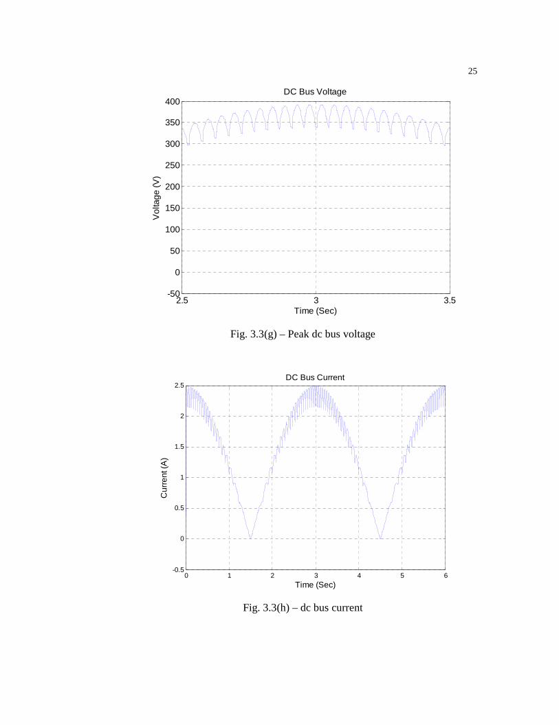
25
2.5 3 3.5-50
0
50
100
150
200
250
300
350
400DC Bus Voltage
Time (Sec)
Vol
tage
(V)
Fig. 3.3(g) – Peak dc bus voltage
0 1 2 3 4 5 6-0.5
0
0.5
1
1.5
2
2.5DC Bus Current
Time (Sec)
Cur
rent
(A)
Fig. 3.3(h) – dc bus current

26
2.5 2.6 2.7 2.8 2.9 3 3.1 3.2 3.3 3.4 3.50
0.5
1
1.5
2
2.5
3DC Bus Current
Time (Sec)
Cur
rent
(A)
Fig. 3.3(i) – Peak dc bus current
The dc bus current figures 3.3(h) and 3.3(i) show the peak current at 2.5A. This
current draw results in a peak power dissipation of approximately 1kW.
WAVIVPpeak 5.9775.26.391ˆˆ =×==
To stiffen the dc bus voltage, a capacitor is placed across the resistive load.
However, a specific capacitance will be required depending upon desired maximum
voltage ripple. The ripple percentage is specified by the difference between the highest
and lowest voltages divided by the RMS voltage level. The capacitance needed for a
specific voltage ripple and energy requirement is shown in equation 3.7. Voltage
ripple is defined by equation 3.8

27
( )2
2)
2
(2
1
ripple
ripple
V
EC
VCE
=
= (3.7)
RMS
lowpeakripple V
VVV
−=% (3.8)
Energy dissipation of 1000W for 3 seconds, half the average wave period, requires
3000 Joules of energy storage. With a combined voltage ripple of 10% (V), requires a
total capacitance of 2.2 Farads. This large capacitance would result in a long transient
period for the simulation to reach steady state. A large capacitance would also increase
the inrush current of the rectifier which may exceed the rating of the armature wire. A
solution around this is to pre-charge the dc bus capacitor to the steady-state voltage
before connecting the generator to the rectifier. Considerations in connecting the
generator to the rectifier need to be done to ensure that the large unloaded generator
voltages do not exceed the ratings of the power electronics. The capacitance chosen
for the next simulation is 0.5F
Voltage: VLLrms = 280V, VLNpk = 228V (0.5F dc capcacitance)
28
0 5 10 15 20 25 30-250
-200
-150
-100
-50
0
50
100
150
200
250Generator Back EMF
Time (Sec)
Vol
tage
(V)
Phase A - Voltage
Phase B - VoltagePhase C - Voltage
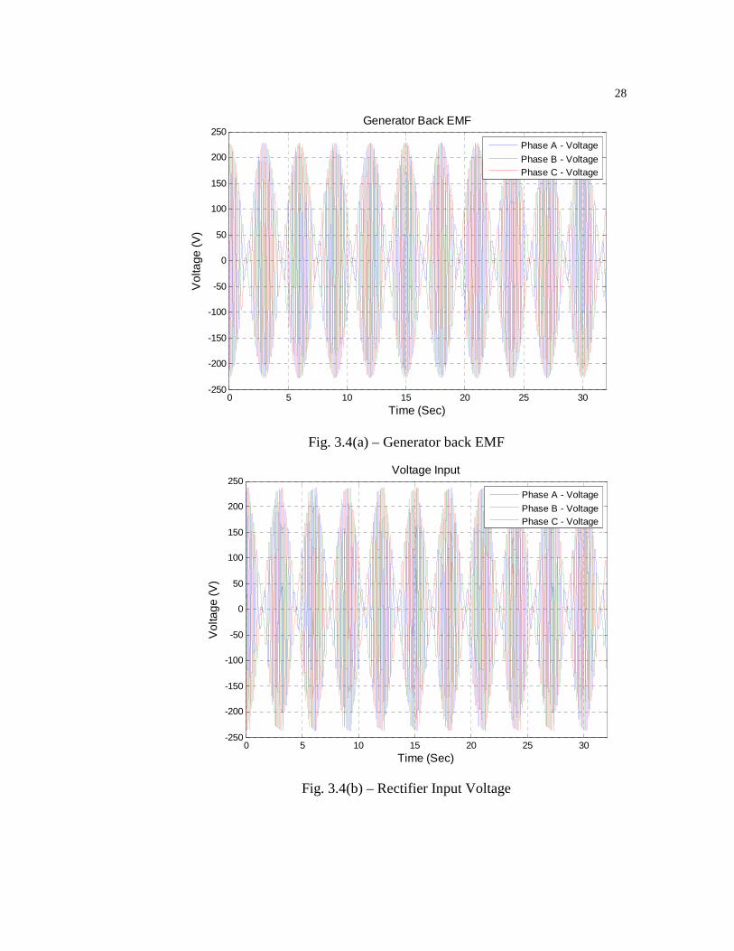
Fig. 3.4(a) – Generator back EMF
0 5 10 15 20 25 30-250
-200
-150
-100
-50
0
50
100
150
200
250Voltage Input
Time (Sec)
Vol
tage
(V)
Phase A - Voltage
Phase B - VoltagePhase C - Voltage
Fig. 3.4(b) – Rectifier Input Voltage

29
Figures 3.4(a) and (b) show the generator back EMF and the input voltage
waveform into the rectifier. The zoomed in figure 3.4(c) shows an even more
pronounced distorted waveform due to the double peak input current.
8.5 8.6 8.7 8.8 8.9 9 9.1 9.2 9.3 9.4 9.5-250
-200
-150
-100
-50
0
50
100
150
200
250Voltage Input
Time (Sec)
Vol
tage
(V)
Phase A - Voltage
Phase B - VoltagePhase C - Voltage
Fig. 3.4(c) – Rectifier input voltage (zoom)

30
0 5 10 15 20 25 30 35-25
-20
-15
-10
-5
0
5
10
15
20
25Generator Output Current
Time (Sec)
Cur
rent
(A)
Phase A - Current
Phase B - CurrentPhase C - Current
Fig. 3.4(d) – Line current
8.5 8.6 8.7 8.8 8.9 9 9.1 9.2 9.3 9.4 9.5-25
-20
-15
-10
-5
0
5
10
15
20
25Generator Output Current
Time (Sec)
Cur
rent
(A)
Phase A - Current
Phase B - CurrentPhase C - Current
Fig. 3.4(e) – Line current (zoom)
31
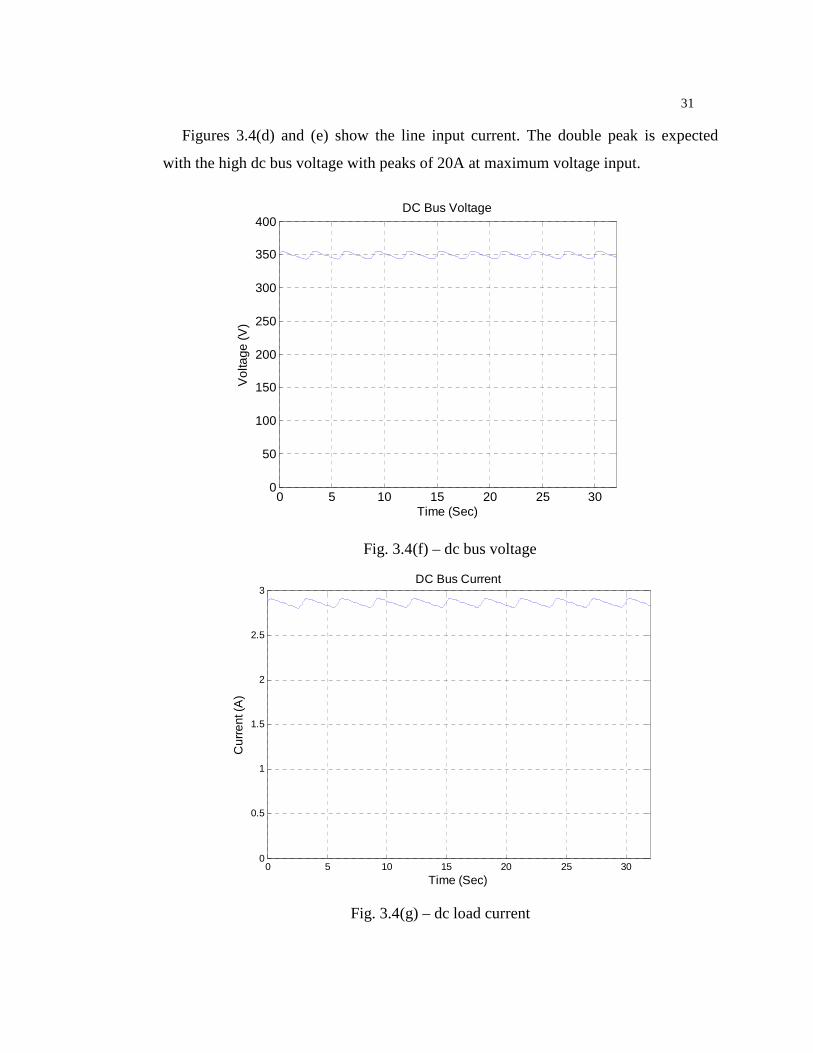
Figures 3.4(d) and (e) show the line input current. The double peak is expected
with the high dc bus voltage with peaks of 20A at maximum voltage input.
0 5 10 15 20 25 300
50
100
150
200
250
300
350
400DC Bus Voltage
Time (Sec)
Vol
tage
(V)
Fig. 3.4(f) – dc bus voltage
0 5 10 15 20 25 300
0.5
1
1.5
2
2.5
3DC Bus Current
Time (Sec)
Cur
rent
(A)
Fig. 3.4(g) – dc load current

32
Figures 3.4(f) and (g) show the dc bus voltage and current. The ripple is low at
approximately 2% (7V). The average dc bus voltage is 350V with an average dc bus
current of 2.86A. The average power dissipated is 1001W with a load resistance of
122Ω .
The next simulation is with a dc bus capacitance of 1100uF. This capacitance will
be used in hardware testing and is a good estimate for those results. Input voltages
from figures 3.5(a) and (b) are similar to the no dc bus capacitance results.
Voltage Input: VLLrms = 280V, VLNpk = 228V, (dc bus capacitance 1100uF)
0 1 2 3 4 5 6-250
-200
-150
-100
-50
0
50
100
150
200
250Generator Back EMF
Time (Sec)
Vol
tage
(V)
Phase A - Voltage
Phase B - VoltagePhase C - Voltage
Fig. 3.5(a) – Generator back EMF

33
0 1 2 3 4 5 6-250
-200
-150
-100
-50
0
50
100
150
200
250Voltage Input
Time (Sec)
Vol
tage
(V)
Phase A - Voltage
Phase B - VoltagePhase C - Voltage
Fig. 3.5(b) –Rectifier input voltage
0 1 2 3 4 5 6-10
-8
-6
-4
-2
0
2
4
6
8
10Generator Output Current
Time (Sec)
Cur
rent
(A)
Phase A - Current
Phase B - CurrentPhase C - Current
Fig. 3.5(c) – Input line current

34
2.5 2.6 2.7 2.8 2.9 3 3.1 3.2 3.3 3.4 3.5-10
-8
-6
-4
-2
0
2
4
6
8
10Generator Output Current
Time (Sec)
Cur
rent
(A)
Phase A - Current
Phase B - CurrentPhase C - Current
Fig. 3.5(d) – Input line current (zoom)
The double peak currents in figure 3.5(c) and (d) are much more pronounced than
the previous simulations. This is due to a varying dc bus voltage that will effect the
commutation of the diodes.

35
0 1 2 3 4 5 60
50
100
150
200
250
300
350
400
450DC Bus Voltage
Time (Sec)
Vol
tage
(V)
Fig. 3.5(e) – Rectifier dc bus voltage
0 1 2 3 4 5 60
0.5
1
1.5
2
2.5
3DC Bus Current
Time (Sec)
Cur
rent
(A)
Fig. 3.5(f) – Rectifier dc bus current

36
The dc bus voltage and current, figures 3.5(e) and (f) show that the dc bus voltage
does not fall to zero like the no dc bus capacitor simulation. This is from the small
1100uF capacitance that results in small amount of energy storage available to the load
when there no input power.
3.3 Summary of Passive Rectifier Results
The double peak is due to the line-to-line diode commutation. As the voltage on the
anode of the diode is at peak it conducts, the other two top diodes are reversed biased
and do not conduct. The bottom diode with the largest negative voltage on the cathode
is forward biased and conducts, the other two diodes do not conduct due to reverse
bias. [5, 7]
Fig. 3.6 – Three-phase diode bridge rectifier
The double peak current results in a non-linear loading and can result in a flat
topping of the line voltage, in the simulations above, only a notch is present due to
very little current draw, but can drastically increase. The double peak current has a
large harmonic content which is injected back to the generator. These harmonics could
potentially damage the linear generator under high loading and continuous operation

37
in a large scale generator. Also, since each diode conducts based on the dc bus
voltage, the buoy will not be controlled and therefore may not be extracting optimum
energy from each wave. Passive rectification would represent a worst-case scenario in
which gating signals from the active rectifier were disabled. Energy extraction from
the generator is still possible and represents a fail-safe mode of operation.
Ideal buoy/generator model was initially simulated with a generator displacement
of 1m, a magnetic wavelength of 144mm and wave period in order to obtain the
desired output phase voltage. The limitation of the ideal model results in an electrical
frequency for a 1m/s wave regardless of actual wave height. If the distance traveled
was changed in the ideal model, more electrical pulses would result. Only eight
electrical pulses are obtainable on the up and eight on the downward-stroke due to
machine design.
Wave Period (s) Wave Height (m) Velocity (m/s) Peak Electrical Frequency
(Hz) 6 1.0 0.524 3.6 8 1.0 0.393 2.7
10 1.0 0.314 2.2
Table 3.1 – Wave height and linear velocity
The electrical parameters are selected to provide baseline results for peak 1kW
power dissipation. The resistive load is selected to dissipate 1kW at the peak of the dc
bus voltage. For example, the 280VLLrms will have a dc load resistance of 156 Ohms
since the dc bus voltage is the peak line-to-line voltage of each phase. Table 2.2 shows
the voltages and the resulting load resistance.
VLNpk VLLrms VLLpk dc bus Load (Ohms) 228 280 396.6 408 156 228 280 396.6 350 122
Table 3.2 – dc bus resistive loads

38
The peak line currents for the no dc bus capacitance and the 1100uF dc bus
capacitance have low peak current values of 2.5A and 6A, respectively. This is within
the current capabilities of the generator windings (12 AWG), however the sustained
1kW simulation with dc bus capacitance of 0.5F results in high currents of 20A.
Sustained currents exceeding the gauge recommendations are detrimental to the
survivability. Results from simulations are summarized in table 1.3.
VLLrms dc bus dc current Capacitance Load (Ohms) Power (W) 280 391V 2.5A X 156.0 977.500 280 350V 2.86A 0.5F 122.0 1001.000 280 408V 2.61A 1100uF 156.0 1064.880
Table 3.3 – Passive rectifier simulation results

39
4 DQ CONTROL
4.1 dq Overview
The concept of dq control is derived from a mathematical transformation to obtain
independent variables of interest: real and reactive power. Real power results in a
change in output torque or for a linear generator, force. The reactive power will
change the flux.
Controlling a full-bridge active rectifier using dq allows independent changes in
real and reactive power. The transformation, from three-phase to two-phase dq, results
in control values that are dc quantities vs. ac control where all control signals are
sinusoidal. The use of dc values allow for elimination of steady state errors.
The three-phase stator in a permanent magnet synchronous machine can be realized
using an equivalent two-phase machine with the phases orthogonal to each other. This
equivalent model decouples the d-axis (direct) and q-axis (quadrature) allowing full
independent control of real torque or reactive power, respectively. The PMLG d-axis
will be aligned with the magnetic north axis and the q-axis will be orthogonal to the
flux. This arrangement controls current with the q-axis and reactive power with the d-
axis. Figure 4.1 shows the projection of these two axes. [3]
3/23/2 )()()( ππ jc
jbas etietitii −++=
r (4.1)
Fig. 4.1 – Three-phase to two-phase projection
40
At time t, the three-phase currents ia(t), ib(t) and ic(t) can be represented by an
equivalent current space vector sir
. The MMF (Magneto-Motive Force), is linearly
dependent on sir
by Ns / p, where Ns is the turns per phase and p is the number of
poles. A pole is defined as north or south, thus two poles would include a north and
south direction. The two orthogonal equivalent windings are each sinusoidally
distributed with sN2
3 turns.
( )
( ) dssqsd
ds
ssqsd
s
ijii
ip
Njii
p
N
v
r
32
23
=+
=+ (4.2)
The d-axis and q-axis currents are scaled when projected on their respective axis.
This can be seen from equation 4.2 shown above. The square root terms relating to
current and turns are used in order to ensure the same MMF distribution as the three-
phase equivalent.
The d and q axis windings are now decoupled magnetically since the flux linkage
of two orthogonal windings is zero. Also, since inductance is proportional to the
number of turns squared the magnetizing inductance is the same as the three-phase
equivalent.
( )( )
mdqm
phasemdqm
phasemdqm
LL
LL
LL
=
=
=
−
−−
−−
,123
,1
2
23
*
*
(4.3)

41
With this, the inductances of the d and q axis can be calculated using equation 4.4.
lsdqmsq
lsdqmsd
LLL
LLL
+=
+=
−
− (4.4)
With the same magnetizing inductance and self-inductance, each dq-winding has
the same inductance as each phase of a three-phase machine. No scaling is necessary.
The relation between the three-phase windings and dq windings needs to be
determined in order for the MMF to be equivalent in both reference frames. The space
vector sir
can be represented from the stator space-vector asir
seen in equation 4.5,
where daθ is the angle between the stator current space-vector and the dq space vector.
dajas
ds eii θ−=
vr
(4.5)
In a three-phase system:
)()()( tititii cbaa
s ++=v
(4.6)
Substituting in equation (4.5) into (4.7) results in:
)3/2()3/2( )()()( πθπθθ +−−−− ++= dadada jc
jb
ja
ds etietietiir
(4.7)
Separating the real and imaginary terms in equation 4.7, results in the
transformation in equation (4.8).

42
+−−−−
+−=
)(
)(
)(
)3
2sin()
3
2sin()sin(
)3
2cos()
3
2cos()cos(
3
2)(
)(
ti
ti
ti
ti
ti
c
b
a
dadada
dadada
sq
sd
πθπθθ
πθπθθ (4.8)
This transformation, known as Park’s Transformation, will be used extensively to
transform three-phase measurements into the dq-axis form. Note however that the
input daθ is the angle difference between the two reference frames and is fixed, but the
magnitudes of the inputs due to varying amplitude input. The sinusoidal shape of the
q-axis reference is a result of the generator force changing polarity as the generator
velocity changes direction. Thus the dq controller will need to track ac values unless
another transformation could theoretically decouple the amplitude modulation
altogether. This ac component term will become apparent in the simulations.
4.2 Transfer Function of Generator
The three-phase active rectifier will apply voltage to the terminals of the permanent
magnet linear generator. The difference in voltage between the back EMF and the
applied terminal voltages determines the current out of the generator. This can be seen
visually in figure 4.2, the per-phase equivalent circuit of the generator/rectifier front
end.
Fig. 4.2 – Per-phase equivalent circuit for PMLG and active recitifer

43
In order to control the generator, the transfer function of the system is needed. The
transfer function relates the output of a system to an applied input. The transfer
function of the PMLG can be obtained from the equations for a Permanent Magnet
Synchronous Machine (PMSM). From the dq stator windings: [1]
βββ
ααα
λ
λ
ssss
ssss
dt
diRV
dt
diRV
+=
+= (4.9)
Multiplying (j) by both sides of the second equation in equation 4.9 combining the
real and imaginary components produces:
βαβαβα λλ ssssssss dt
dj
dt
dijRiRjVV +++=+ (4.10)
Transforming from the alpha/beta stationary coordinates to the dq rotating
coordinates, substitute the following equations (4.11) and (4.12) in to equation (4.10).
βαα
βαα
βαα
λλλ sss
sss
sss
j
jiii
jVVV
+=
+=
+=
r
v
v
(4.11)
da
da
da
jdss
jdss
jdss
e
eii
eVV
θα
θα
θα
λλvv
vv
vv
=
=
=
(4.12)

44
The result is equation 4.15, after differentiation (equation 4.14) with applied chain
rule, can be separated into their respective d and q components. This will allow the
controller to independently control the real power and reactive power.
( )
( ) dadadada
dadada
jds
jds
jdss
jds
jds
jdss
jds
ejedt
deiReV
edt
deiReV
θθθθ
θθθ
λωλ
λ
vvvv
vvv
++=
+= (4.13)
( ) ( ) ( )sqsdsqsdsqsdssqsd
sqsdsd
jjdt
djiiRjVV
jVVV
λλωλλ −++++=+
+=r
(4.14)
sdsqsqssq
sqsdsdssd
dt
diRV
dt
diRV
ωλλ
ωλλ
++=
−+= (4.15)
Taking equation (4.15) and transforming it into the frequency domain via the
Laplace transform results in:
sdsqsqssq
sqsdsdssd
siRV
siRV
ωλλωλλ
++=
−+= (4.16)
Substituting the flux linkage with the respective dq inductance values and currents:
( ) ( )( )fdsdssqssqssq
sqsfdsdssdssd
fdsdssd
sqssq
iLisLiRV
iLiLsiRV
iL
iL
λωωλ
λλλ
+++=
−++=
+=
=
(4.17)

45
The control scheme will have cross-coupling effects due to the d-axis stator voltage
dependent upon the q-axis current as well as the q-axis voltage dependent upon the d-
axis current. This will introduce disturbances that the controller will need to
compensate for.
4.3 Controller Design
The controller design will be based on a single-input single-output (SISO) control
topology. This controller is in series with the plant and is shown in figure 4.18. The
plant is the device being controlled; in this case it is the PMLG. [8]
Fig. 4.3 –Control topology
)()()(
)(*)()(
)(*)()(
sYsRsE
sEsGsU
sUsGsY
c
p
−==
=
(4.18)
Substituting and solving for Y(s)/R(s), where Y(s) is the output and R(s) is the
input in the s-domain:

46
( )
( )
1)()(
)()(
)(
)(
)()()()()(1)(
)()()()()()()(
)()()()()(
+=
=+
−=
−=
sGsG
sGsG
sR
sY
sRsGsGsGsGsY
sYsGsGsRsGsGsY
sYsRsGsGsY
cp
cp
cpcp
cpcp
cp
(4.19)
The result is the total closed-loop gain of the system.
The plant and controller transfer functions are shown in equation 4.22 and 4.23.
The controller is PI (proportional-integral) controller. The proportional gain value
accelerates the error increasing convergence time, reducing the rise time but
increasing overshoot. The integral gain will decrease rise time and increase overshoot,
however it will eliminate steady-state errors. The elimination of steady-state errors is
highly desired in precise controls. There exists a derivative part for a PID controller,
which reduces overshoot, however if the controllers performance does not have
substantial overshoot, the derivative term may not be necessary.
The plan transfer function is derived from equation 4.17 in the previous section.
Since generator force is related to generator current, current control is desired for this
topology. Current referenced will be the input to the controller; the output will be
applied terminal voltages to the generator.
( ) ( )( ) ( )fdsdssssqsq
sqsfdsssdsd
iLsLRiV
iLssLRiV
λωωλ+++=
−++= (4.20)
Equation 4.20 is rewritten terms of the generator output current to the terminal
voltages, equation 4.21. Since both the stator resistance and inductance are equivalent
in the dq reference frame, the same plant can be used for the controller design.

47
( ) ( )
( )sssdssd
sd
ssfdsdssq
sq
sLRiLV
i
sLRiLV
i
+=
+
+=
++
1
1
ω
λω (4.21)
The plant transfer function is described in equation 4.22, where Ls is the stator
inductance and Rs is the stator coil resistance.
ssp RsL
sG+
= 1)( (4.22)
s
K
Ks
KsG
Ks
KsG
i
p
ic
pi
c
+
=
+=
1
)(
)(
(4.23)
The transfer function of a PI controller is shown in equation 4.23. It is typical to
expand the integral term to aid in the calculations of the gain values. The total loop
gain can be expressed as the multiplication of both the controller and plant transfer
functions. It is common to cancel out the pole of the first term with the zero of the
second term.
The plant transfer function shown in figure 4.4 is stable with the phase margin at
34.5 rad/sec. With no controller, this system will oscillate towards steady state values.
The 3dB point at Ra/La = 23.33 rad/sec is noted. The pole at this frequency will pull
the phase margin towards -90 degrees. The pole of the integrator is at zero rad/sec
(1dB) and adding any more poles will bring the phase shift down more. By canceling
out the plant pole with controller zero, the phase margin will stay at -90 degrees.
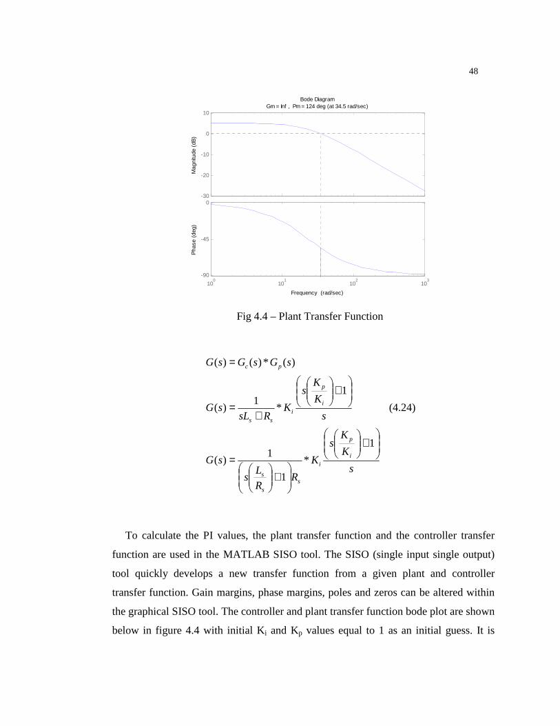
48
-30
-20
-10
0
10
Mag
nitu
de (
dB)
100
101
102
103
-90
-45
0
Pha
se (
deg)
Bode DiagramGm = Inf , Pm = 124 deg (at 34.5 rad/sec)
Frequency (rad/sec)
Fig 4.4 – Plant Transfer Function
s
K
Ks
K
RR
Ls
sG
s
K
Ks
KRsL
sG
sGsGsG
i
p
i
ss
s
i
p
iss
pc
+
+
=
+
+=
=
1
*
1
1)(
1
*1
)(
)(*)()(
(4.24)
To calculate the PI values, the plant transfer function and the controller transfer
function are used in the MATLAB SISO tool. The SISO (single input single output)
tool quickly develops a new transfer function from a given plant and controller
transfer function. Gain margins, phase margins, poles and zeros can be altered within
the graphical SISO tool. The controller and plant transfer function bode plot are shown
below in figure 4.4 with initial Ki and Kp values equal to 1 as an initial guess. It is

49
noted that by canceling out the pole of the plant with the zero of the controller, Kp/K i
will be known. Kp/K i is calculated to be 0.0428.
-40
-20
0
20
40
60
Mag
nitu
de (
dB)
10-2
10-1
100
101
102
103
-90
-60
-30
0
Pha
se (
deg)
Bode DiagramGm = Inf , Pm = 122 deg (at 34.5 rad/sec)
Frequency (rad/sec)
Fig. 4.5 – Bode plot of plant and controller open-loop transfer function
( )( ) 56.0104286.0
1)(
24
56.0
1
1)(
++=
=Ω=
+
+=
ss
ssG
mHL
R
RR
Lss
ssG
s
s
ss
s
(4.25)
From equation 4.25, there should be a zero at ω = 1 rad/sec and a pole at ω =
1/0.04286 = 23.3 rad/sec.
50
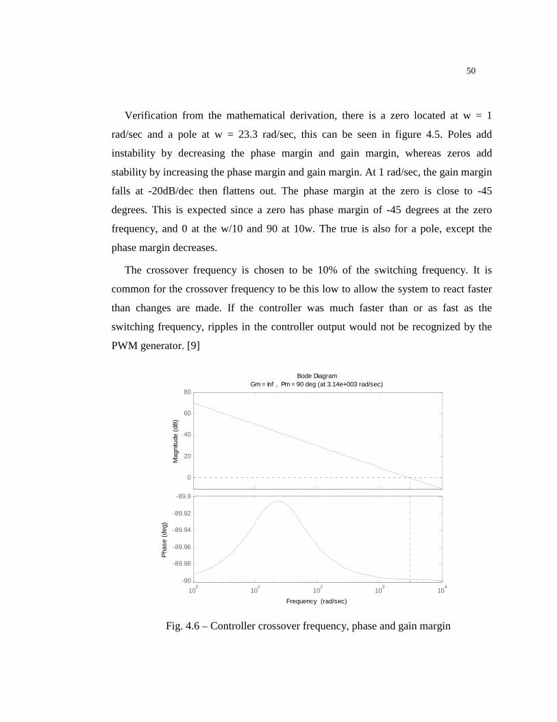
Verification from the mathematical derivation, there is a zero located at w = 1
rad/sec and a pole at w = 23.3 rad/sec, this can be seen in figure 4.5. Poles add
instability by decreasing the phase margin and gain margin, whereas zeros add
stability by increasing the phase margin and gain margin. At 1 rad/sec, the gain margin
falls at -20dB/dec then flattens out. The phase margin at the zero is close to -45
degrees. This is expected since a zero has phase margin of -45 degrees at the zero
frequency, and 0 at the w/10 and 90 at 10w. The true is also for a pole, except the
phase margin decreases.
The crossover frequency is chosen to be 10% of the switching frequency. It is
common for the crossover frequency to be this low to allow the system to react faster
than changes are made. If the controller was much faster than or as fast as the
switching frequency, ripples in the controller output would not be recognized by the
PWM generator. [9]
0
20
40
60
80
Mag
nitu
de (
dB)
100
101
102
103
104
-90
-89.98
-89.96
-89.94
-89.92
-89.9
Pha
se (
deg)
Bode DiagramGm = Inf , Pm = 90 deg (at 3.14e+003 rad/sec)
Frequency (rad/sec)
Fig. 4.6 – Controller crossover frequency, phase and gain margin

51
By canceling out the zero and pole or by moving the zero over the pole location in
the SISO tool GUI, the results are shown in figure 4.5.
The new controller transfer function now has a crossover frequency of 3150 rad/sec
which is approximately 10% of the 5kHz (31krad/sec) switching frequency. The phase
margin is -90 degrees, ensuring system stability. Any phase margin larger than 180
degrees will be unstable and any phase margin close to 180 can have large oscillations
before steady-state is reached. The SISO tool gives the controller a new transfer
function shown in equation 4.26.
( )s
ssGc
043.011760
+= (4.26)
From the previous controller equation, the values for Ki and Kp can be found.
Looking at equation 4.26, Ki is the overall gain equal to 1760 and since Kp/K i = 0.043,
Kp is 75.6. These values will be used in the PI controller for the simulations.
An average model can be constructed to evaluate how effective the controller is.
The average model will eliminate the switching dynamics from the model that are
present with simulations done with active elements. The switching dynamics add
another level of complexity to the model that does not necessarily help evaluate the
performance of the controller. The switching elements also involve slower
computation time and different simulation solvers in order to compensate for active
switching elements.
To construct the switching model, the transfer function of the controller and the
plant with feedback are arranged as seen in figure 4.7.

52
Fig. 4.7 – Loop gain control topology
The switching model takes in terminal dq-voltages, normalizes the value and sent
to the PWM (switching) block. The PWM will regulate the average voltage applied to
the generator terminals. This is a physical model representation.
Fig. 4.8 – Average model
The average model eliminates the switching block and the dynamics created from
the IGBT switching. This assumes ideal PWM generation and no losses.
Fig. 4.9 – Equivalent circuit for the active rectifier
The per-phase equivalent circuit of the three-phase converter is shown above in
figure 4.9. The left hand side represents the dc bus and the right hand side represents

53
the permanent magnet linear generator. The [v]abc is the rectifier applied PWM voltage
signals, the [Vs]abc is the PMLG back EMF. The controller outputs the necessary
terminal voltage, so for the average model, no PWM block is necessary.
Fig. 4.10 – Controller layout
Fig. 4.11 – Simulink controller layout
Implementing the dependent voltage source is done with the SimPowerSystems
dependent dc voltage source block. The direct output of the controller is fed into the
dependent voltage source. The decoupling terms are connected to the output of the PI
controller to eliminate the coupling terms within the plant. This will provide increased
performance for the system.

54
Fig. 4.12 - Average model in Simulink
4.4 Controller Verification
Testing the verification of the controller is done using the step feature in
MATLAB. The cascade controller transfer function is expressed in equation 4.27. The
step response of the close loop system T(s) is shown below. The step response test will
show how quickly the system will converge to unity, the referenced input.
s
K
Ks
K
RR
Ls
sGi
p
i
ss
s
+
+
=
1
*
1
1)( (4.27)

55
ssss
ssssT
s
K
Ks
K
RR
Ls
s
K
Ks
K
RR
Ls
sT
sG
sGsT
i
p
i
ss
s
i
p
i
ss
s
98045.84833.1000576.0
98014.84806.1)(
1
1
*
1
1
1
*
1
1
)(
1)(
)()(
234
23
+++++=
+
+
+
+
+
=
+=
(4.28)
0 0.5 1 1.5 2 2.5 3 3.5 4 4.5 5
x 10-3
0
0.2
0.4
0.6
0.8
1
System: TTime (sec): 0.0025Amplitude: 1
Step Response
Time (sec)
Am
plitu
de
Fig. 4.13 – Step response of closed-loop controller and plant

56
From figure 4.13, the system reaches unity output at 2.5ms. This convergence time
is very acceptable since the switching period is 200us (5 kHz). Also, no oscillation is
present.

57
5 THREE-PHASE SYNCHRONOUS ACTIVE RECTIFIER
5.1 Active Rectifier Overview
Three-phase active rectifiers allow for a greater range of control of the real and
reactive input power, resulting in better control of the PMLG. Three-phase active
rectifiers are built using six IGBT switches which are modulated on and off. This
modulation controls the magnitude and frequency of the rectifier phases. Contrast this
to the passive rectifier where no control is obtained since current draw is determined
by the dc bus voltage. Since line currents can be controlled, the generator force is
controlled. [5]
The active rectifier topology is similar to an inverter for motor control. An inverter
voltage output is limited to the dc bus voltage. The dc bus voltage used in the testing
of the PMLG is 1000V, allowing full current control up to 612VLLrms. If the input
voltage exceeds this, the current cannot be controlled well.
Each IGBT module has built in anti-parallel diodes for current to conduct when
gating signals are disabled. In the event of gating signal failure, the generator/rectifier
will still be able to supply power to the dc load under passive rectification mode. This
is important in a scenario when sustained power is critical.
5.2 Ideal Wave Model Simulations
The ideal wave model interfaced with the SimPowerSystems block will establish
the base testing for the three-phase active rectifier. The controller accuracy will be
tested using a step change in current and sinusoidal current reference. Generator back
EMF voltages of VLLrms=280V will be simulated. This voltage represents a 0.7 m/s
linear velocity.

58
5.2.1 Switching Model
The three-phase IGBT active rectifier is connected to a variable load which is
represented by the dc-dc converter. The dc-dc converter is controlled by a hysteretic
controller which maintains the dc bus voltage at an average 1000V. The load resistor
is 100 Ohms. The IGBT Simulink model contains snubber circuits to reduce high
voltages spikes during switching events due to the IGBTs. The snubber circuits are
parallel RC components designed to handle switching power dissipation. Switching
frequency is set at 5 kHz.
Fig. 5.1 – Three-phase active rectifier with dc bus regulator
Fig. 5.2 – dq-control Simulink model

59
The Iq_ref block is the input reference q-axis current. The first simulation will set
Iq_ref to a sinusoidal current draw at T = 6s, 0.167Hz, with a peak amplitude of 10A
0 1 2 3 4 5 6-800
-600
-400
-200
0
200
400
600
800Active Rectifier Applied Voltage
Time (s)
Vol
tage
(V
)
Fig. 5.3(a) – Active Rectifier Applied Voltage (280VLLrms)
In figure 5.3(a), the applied voltage from the active rectifier is a PWM voltage.
The voltage seen is measured from phase-to-neutral.
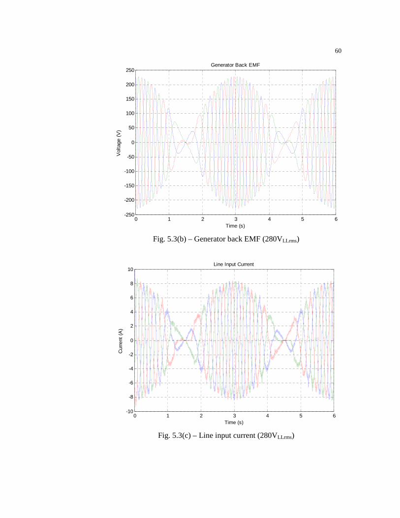
60
0 1 2 3 4 5 6-250
-200
-150
-100
-50
0
50
100
150
200
250Generator Back EMF
Time (s)
Vol
tage
(V
)
Fig. 5.3(b) – Generator back EMF (280VLLrms)
0 1 2 3 4 5 6-10
-8
-6
-4
-2
0
2
4
6
8
10Line Input Current
Time (s)
Cur
rent
(A
)
Fig. 5.3(c) – Line input current (280VLLrms)

61
In figure 5.3(c), the current waveform input is not as smooth as expected. The
current is in phase with the voltage input waveform giving unity power factor,
however the slow switching frequency at 5kHz has caused large ripples in the line
current. Increasing the switching frequency to 10 kHz or more will reduce the current
ripple yielding a cleaner input waveform and no reverse dc bus current.
0 1 2 3 4 5 60
100
200
300
400
500
600
700
800
900
1000
DC Bus Voltage
Time (s)
Vol
tage
(V
)
Fig. 5.3(d) – dc bus voltage
The dc bus voltage is shown in figure 5.3(d). The voltage ripple is 20V from
1010 to 990. This is maintained by the dc-dc converter.

62
0 1 2 3 4 5 6
-1
0
1
2
3
4
5
6
7
8
9
10dc bus Current
Time (s)
Cur
rent
(A
)
Fig. 5.3(e) – dc bus current into capacitor
Figure 5.3(e) shows the current into the dc capacitor. There is no reverse current
until the simulation reaches 1.25 seconds and is sustained for half a second. This
reverse current is from the noisy line input current during this time, allowing current to
flow back to the generator.

63
0 1 2 3 4 5 6-15
-10
-5
0
5
10
15Controller Isq measured vs. reference
Time (s)
Cur
rent
(A
)
Isq Measured
Isq
Reference
Fig. 5.3(f) – Isq measured vs. reference
0 1 2 3 4 5 6-15
-10
-5
0
5
10
15Controller I
sd measured vs. reference
Time (s)
Cur
rent
(A
)
Isd
Reference
Isd
Measured
Fig. 5.3(g) – Isq measured vs. reference

64
Figures 5.3(f) and (g) show excellent tracking of the reference currents Isq and
Isd. The measured values show a rippled that is due to the switching IGBTs and would
be reduced by increasing the switching frequency.
5.2.2 Average Model
Running the average switching model will eliminate the current ripples seen in
the switching model simulations. A step function will change the input reference
current level at time t = 1s into the simulation from 2A to 5A. The input reference and
the measured current level can be seen in figure 5.4.
0.5 1 1.5 2 2.5
0
1
2
3
4
5
Isdq Output
Time (Sec)
Cur
rent
(A)
Isd
Isq
Fig. 5.4(a) – Isdq current output
Above in figure 5.4, shows the Isdq current output of the PMLG. The step change
applied at 1 second can be seen from 2A to 5A. The low frequency component from
the Isq measurement is due to controller tracking an ac value from the decoupling
compensation terms. The output of the dq transform is normally dc values for a
constant amplitude signal, however the variable amplitude nature of the generator
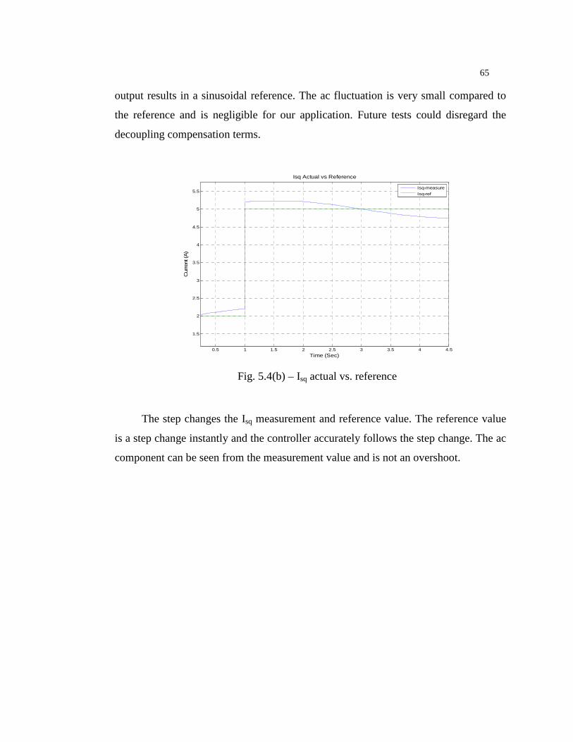
65
output results in a sinusoidal reference. The ac fluctuation is very small compared to
the reference and is negligible for our application. Future tests could disregard the
decoupling compensation terms.
0.5 1 1.5 2 2.5 3 3.5 4 4.5
1.5
2
2.5
3
3.5
4
4.5
5
5.5
Isq Actual vs Reference
Time (Sec)
Cur
rent
(A)
Isq-measure
Isq-ref
Fig. 5.4(b) – Isq actual vs. reference
The step changes the Isq measurement and reference value. The reference value
is a step change instantly and the controller accurately follows the step change. The ac
component can be seen from the measurement value and is not an overshoot.

66
0.5 1 1.5 2 2.5 3 3.5 4 4.5 5 5.5
-4
-3
-2
-1
0
1
2
3
4
x 10-3 Isd Actual vs Reference
Time (Sec)
Cur
rent
(A)
Isd-ref
Isd-measure
Fig. 5.4(c) – Isd actual vs. reference
The Isd measurement and reference values can be seen in figure 5.4(c). The
reference value for the d-axis current is set to zero. This will provide no reactive
power draw from the PMLG. The actual Id value also exhibits the low frequency ac
component. The error on the ac component compared to the reference value is
negligible. The max error current value is 0.5mA, negligible compared to real q-axis
component of 5A. The cross-coupling factor is exhibited at t = 1s, noted by the spike
in current.
A sinusoidal current draw with the same frequency of the wave excitation force
is shown in the simulations below. The peak current will correspond to the peak
velocity and no current draw at zero velocity (the top of an ocean wave). VLLrms of
280V corresponding to 0.7m/s velocity will be simulated.
Voltage: VLLrms = 280V

67
0 1 2 3 4 5 6 7 8-250
-200
-150
-100
-50
0
50
100
150
200
250Generator Output Voltage
Time (s)
Vol
tage
(V
)
Fig. 5.9(a) – Generator output voltage
0 1 2 3 4 5 6 7 8-250
-200
-150
-100
-50
0
50
100
150
200
250Active Rectifier Input Voltage
Time (s)
Vol
tage
(V
)
Fig. 5.9(b) – Active rectifier input voltage

68
0 1 2 3 4 5 6 7 8-6
-4
-2
0
2
4
6
8Active Rectifier Input Current
Time (s)
Cur
rent
(A
)
Fig. 5.9(c) – Active rectifier input current
The active rectifier input voltages and currents are in phase, producing unity
power factor. This can be seen by comparing figure 5.9(b) with 5.9(c), noting the zero
crossings for each waveform.

69
0.5 1 1.5 2 2.5 3 3.5 4 4.5 5 5.5
-8
-6
-4
-2
0
2
4
6
8
10
12
Isdq Output
Time (Sec)
Cur
rent
(A)
Isd
Isq
Fig. 5.9(d) – Sinusoidal Isq current output
0.5 1 1.5 2 2.5 3 3.5 4 4.5 5 5.5-2.5
-2
-1.5
-1
-0.5
0
0.5
1
1.5
2
2.5
x 10-3 Isd Actual vs Reference
Time (Sec)
Cur
rent
(A)
Isd-ref
Isd-measure
Fig. 5.9(e) – Isd actual vs. reference

70
0 1 2 3 4 5 6-5
-4
-3
-2
-1
0
1
2
3
4
5Isq Actual vs Reference
Time (Sec)
Cur
rent
(A)
Isq-measure
Isq-ref
Fig. 5.9(f) – Isq actual vs. reference
The sinusoidal reference current is tracked with only a slight phase shift seen in
figure 5.6(f). The amplitude matches the reference value and a slight phase shift.
5.3 Dynamic Model
The dynamic model simulation combines the dynamic PMLG model and the dq
controller. There are no SimPowerSystems block interfaces. The Simulink model is
shown in figure 5.10 with a sinusoidal reference current. Note the de-coupling
compensation terms.

71
Fig. 5.10 – Dynamic PMLG and controller Simulink model
The first simulation will step the input reference current Isq at t = 1s from 2A to 5A
to show the response time of the controller.
0 0.5 1 1.5 2 2.51
1.5
2
2.5
3
3.5
4
4.5
5
5.5
6Controller I
sq measured vs. reference
Time (s)
Cur
rent
(A
)
Isq
measured
Isq
reference
Fig. 5.11(a) – Isq current measured vs. reference
The step change seen in figure 5.11(a) shows the measured Isq tracking the
reference value perfectly. No ac component seen due to de-coupling compensation
terms.

72
0 0.5 1 1.5 2 2.5-1
-0.8
-0.6
-0.4
-0.2
0
0.2
0.4
0.6
0.8
1Controller I
sd measured vs. reference
Time (s)
Cur
rent
(A
)
Isd
reference
Isd
measured
Fig. 5.11(b) – Isd current measured vs. reference
Figure 5.11(b) showing the Isd current measured tracks well to the desired
reference value. With exactly zero Id current, there is no reactive power draw from the
generator producing unity power factor. No ac component with the de-coupling
compensation terms.
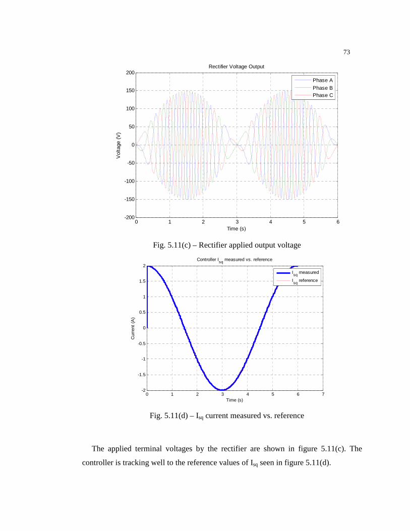
73
0 1 2 3 4 5 6-200
-150
-100
-50
0
50
100
150
200Rectifier Voltage Output
Time (s)
Vol
tage
(V
)
Phase A
Phase BPhase C
Fig. 5.11(c) – Rectifier applied output voltage
0 1 2 3 4 5 6 7-2
-1.5
-1
-0.5
0
0.5
1
1.5
2Controller I
sq measured vs. reference
Time (s)
Cur
rent
(A
)
Isq
measured
Isq
reference
Fig. 5.11(d) – Isq current measured vs. reference
The applied terminal voltages by the rectifier are shown in figure 5.11(c). The
controller is tracking well to the reference values of Isq seen in figure 5.11(d).

74
0 1 2 3 4 5 6 7-1
-0.8
-0.6
-0.4
-0.2
0
0.2
0.4
0.6
0.8
1Controller I
sd measured vs. reference
Time (s)
Cur
rent
(A
)
Isd
reference
Isd
measured
Fig. 5.11(e) – Isd current measured vs. reference
Again, with the sinusoidal input reference current, there is little oscillation in the Isd
measured values. This result is unity power factor and with no reactive power draw
from the generator. The controller is matched perfectly with the generator model.
5.4 Stochastic Wave Simulations
The stochastic wave simulation will reflect more of a real world environment. The
stochastic model will generate a random sea environment of various wave periods and
frequency determined by a wave energy frequency spectrum. A designed optimum
force controller will command a reference force for the generator to exert determined
by the sea state. The current designed controller must track a prescribed force
command accurately. This simulation will use a pre-existing wave generator and
optimum force controller. [10]

75
Fig. 5.12 – Force input block
fdrefq
Fi
λτ2
_ = (5.1)
The force input block will output the reference iq-axis current, from a commanded
force input, seen in equation 5.1
0 5 10 15 20 25 30 35 40 45 50-2
-1.5
-1
-0.5
0
0.5
1
1.5
2Random Sea State
Time (s)
Ocean Wave
Buoy PositionWave Exiciation Force
Buoy Velocity
Fig. 5.13(a) – Stochastic sea state
The blue line in figure 5.13(a) shows the ocean wave height and the green line
represents the buoy position. The optimum force controller will prescribe a force
required by the PMLG. This force is seen in figure 5.13(b)

76
0 5 10 15 20 25 30 35 40 45 50-6000
-4000
-2000
0
2000
4000
6000
8000
10000
12000Buoy Force Control Tracking
Time (s)
For
ce (
N)
Force Reference
Force Generated
Fig. 5.13(b) – Generated prescribed force reference and measured
The controller performance is seen in figure 5.13(b). The controller tracks the
prescribed generator force with very little phase shift or amplitude shift. The actual
graphs are shown to be exactly on top of each other.

77
0 5 10 15 20 25 30 35 40 45 50-10
-5
0
5
10
15
20
Isq
Current Measured vs. Reference
Time (s)
Cur
rent
Isq
Measured
Isq
Reference
Fig. 5.13(c) – Commanded current reference and measured
The force command is computed to a current Isq reference. Fig, 5.13(c) shows that
the controller tracks the prescribed current waveform well.
0 5 10 15 20 25 30 35 40 45 50-150
-100
-50
0
50
100
150Active Rectifier Applied Voltage
Time (s)
Vol
tage
(V
)
Phase A
Phase BPhase C
Fig. 5.13(d) – Active rectifier applied voltage

78
In figure 5.13(d) the active rectifier terminal voltages are shown. These terminal
voltages control the current from the generator.

79
6 GATING SIGNAL GENERATION
6.1 Pulse Width Modulation
The gating signals applied to the IGBT switches are designed to generate a Pulse
Width Modulated (PWM) signal output. This PWM output average is sinusoidal with
added harmonic content depending on the switching frequencies and phase
connections. This section will focus on two PWM generation techniques used widely
in industrial drive applications.
6.2 Sine-Triangle PWM
SPWM (Sine-Triangle Pulse Width Modulation) is a technique for generating the
necessary gating signals on a converter or inverter. Sine-Triangle PWM is easy to
implement and requires little processing power for the gating signal generation.
By switching each required IGBT on and off, the voltage output with reference to
the neutral of the wye-connected phases will generate a voltage pulse.
Fig. 6.1 – Three-Phase IGBT Bridge

80
In the above figure 6.1, the IGBT switches with labels are shown. The control
signals are from the dq to abc output block. These control signals have a peak height,
Vcontrol,peak for each phase. Taking a single phase A for example [5]:
)(2
)(1
,
,
onQvv
onQvv
triacontrol
triacontrol
→≤→≥
When the control signal of phase-a is larger than the triangle comparison wave,
the turn the top leg on, thus the voltage output v_an = +Vdc, if the control signal is
less than the triangle wave, then v_an = -Vdc. The equivalent will happen with phase-
b, legs Q3 and Q4, and phase-c, legs Q5 and Q6, except the control signals will be
phase shifted by -120 and +120 degrees, respectively. When computing the line-to-
line voltage, for example between phase-a and phase-b, vab = v_an – v_bn.
The PWM generator was implemented in Simulink shown in figure 6.1.
Fig. 6.2 – PWM generator with dead-time
The v_control signal input is from the dq to abc transformation. These values are
the voltage control values for each phase. For an inverter the peak phase-to-neutral
fundamental value is specified by equation 6.1.

81
( )2
ˆ1
dcaLNpeak
VmV = (6.1)
The modulation ratio index, ma is the ratio of the peak control voltage level to the
peak triangle wave value. For the generated triangle wave, Vtri, the amplitude is 1V.
The maximum peak output phase-to-neutral voltage is 500V or 612VLLrms for a dc bus
of 1000V and 300V or 367VLLrms for a 600V dc bus.
The dead-time generator will space the gating on signals by shift the triangle waves
by the amount within the dead-time block in figure 6.2. The dead-time will prevent
both top and bottom IGBTs from turning on at the same time and shorting the dc bus.
The dead-time is necessary due to the specified rise/fall time and turn-on/off delay of
the IGBT device.

82
7 DC-DC Converter
The current generated from the PMLG will charge the dc bus voltage. For a
single buoy test design, current will vary depending upon wave conditions, force
prescribed and current controller requirements. The purpose of the dc-dc converter is
to maintain the 1000V dc bus by regulating the current delivered to a resistive load
bank.
For a single 1kW generator test setup dc-dc converter will be located on the
same interface as the three-phase active rectifier. The resistive load bank will be
located on the test vessel with data acquisition equipment. The resistive load bank will
be used to dissipate the power generated. The active rectifier will be located inside the
spar of the generator. The small test setup is shown in figure 7.1.
Fig. 7.1 – Test system setup
For a future 12kV high voltage dc (HVDC) transmission, one or more
generators are arranged to a common 1000V dc bus. The dc-dc converter in this case
is designed to regulate the 1000V dc bus and boost the voltage to 12kV for
transmission to shore. If the future setup will include back driving the PMLGs, a bi-
directional dc-dc converter would need to be implemented.
Fig. 7.2 – Future test setup

83
For the small setup, comparing it to the larger future setup, the dc-dc converter
and load for the 1kW test setup will act like the dc-dc converter, HVDC transmission,
inverter, and utility grid interface in the 12kV setup.
7.1 Model Descriptions
7.1.1 Boost Circuit
Fig. 7.3 – Boost circuit layout
The boost circuit converts the input voltage Vdc to an output voltage Va where
Va is greater than Vdc. When the IGBT is switched on by a gating signal, the diode is
reversed biased due to the voltage drop across the emitter-collector being of a smaller
value than the output voltage, Vdc. The current within the inductor will ramp up
linearly with large inductance values. Note that energy is proportional to the square of
turn on time [11].
L
tVI
t
IL
dt
diLV
ondc
ons
=∆
∆== (7.1)
L
tVLIE ondc
22
1 222 == (7.2)
When the IGBT is switched off, the current in the inductor cannot change
instantaneously, thus the voltage polarity is reversed to maintain a flowing current.

84
The inductor delivers its energy to the load, capacitor and diode until the IGBT is
switched on again.
TDt
DTt
t
IIL
dt
diLVV
off
on
offadc
)1(
12
−==
−==−
(7.3)
D
II
D
VV
adc
dca
−=
−=
1
1 (7.4)
When noted that the peak-to-peak current ripple through the inductor is the same
then both equations can be combined to form the average output voltage Va and Idc.
For the Vdc bus to maintain 600V the buck circuit will need to regulate the current
drawn from the capacitor. When Vdc drops below the 1000V reference, the PI
controller reduces the duty ratio of the IGBT, drawing less energy from the capacitor
and thus raising the capacitor voltage. When Vdc increases above the reference, the PI
increases the error, increasing the duty ratio which draws more energy from the
capacitor and decreases its voltage.
7.1.2 Buck Circuit
Fig. 7.4 – Buck circuit layout

85
The buck circuit converts the input voltage Vdc to an output voltage Va where
Vdc is greater than Va. The relationship of the output voltage to input voltage is
described by equation 7.5.
10 <<=D
DVV dca (7.5)
When the IGBT is switched on, diode is reversed biased and current will begin
to charge up the inductor since Vdc is greater than the load voltage Va.
adc
on
VVtv
t
IL
dt
diLtv
−=
∆==
)(
)( (7.6)
The voltage across the inductor will change at a rate shown in equation 7.6.
When the IGBT is switched off, current in the inductor cannot change instantaneously
resulting in a polarity change in voltage across the inductor. This polarity change
forward biases the diode allowing current to flow in the circuit. The energy in the
inductor flows to the load until it is depleted.
offoff t
ILVa
t
IILVa
∆=⇒−
=− 21 (7.7)
Peak to peak ripple current is equivalent in steady state as state in equations 7.8,
below.
DVV
TDt
DTtL
tVV
L
tVI
dca
off
on
onadcoffa
=
−==
−==∆
)1(
)(
(7.8)
86
Since the input voltage needs to be maintained the amount of current flowing
from Vdc to the load is regulated. To regulate the current from the source to the load
control of the IGBT switch duty cycle is changed with a feedback loop referencing the
desired input voltage. A control loop references 1000V as the desired input voltage. If
more current is delivered to the load than the generator can provide the input voltage
will decrease past 1000V. The PI controller integrates the negative error,
accumulating, and thus the duty ratio decreases; vcontrol will decrease lowering the
overall duty ratio until steady state has occurred.
Determining the component values can be calculated based on mathematical
analysis of the buck converter circuit. The peak to peak capacitor ripple voltage can be
expressed in equation 7.9.
28
)1(
8 s
s
sc LCf
DDV
Cf
Iv
−=∆=∆ (7.9)
7.2 Resistive Loading
For the boost circuit, the load resistance would need to be high enough such that
when the regulating IGBT is turned off during low generator velocity, the time
constant of the RC circuit is such that the voltage across the capacitor never decays
below that of the Vdc bus. If the voltage across the load resistor is less than the Vdc
bus, the diode will be forward biased and will collapse the dc bus voltage.
The load resistance connected to the dc bus needs to dissipate a peak power of
1kW. The average power will be defined as the power over a complete ocean wave
cycle. A load resistance required to dissipate 1000W at a 1000V dc bus voltage is
calculated below in equation 3.6, where P is total power, Vdc is dc bus voltage, Idc is dc
bus current, and Rload is the load resistance.
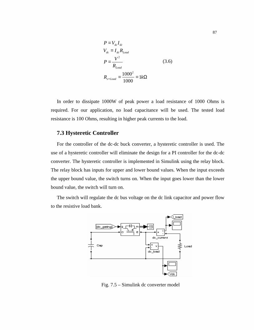
87
Ω==
=
==
= kR
R
VP
RIV
IVP
Loads
Load
Loaddcdc
dcdc
1100010002
2
(3.6)
In order to dissipate 1000W of peak power a load resistance of 1000 Ohms is
required. For our application, no load capacitance will be used. The tested load
resistance is 100 Ohms, resulting in higher peak currents to the load.
7.3 Hysteretic Controller
For the controller of the dc-dc buck converter, a hysteretic controller is used. The
use of a hysteretic controller will eliminate the design for a PI controller for the dc-dc
converter. The hysteretic controller is implemented in Simulink using the relay block.
The relay block has inputs for upper and lower bound values. When the input exceeds
the upper bound value, the switch turns on. When the input goes lower than the lower
bound value, the switch will turn on.
The switch will regulate the dc bus voltage on the dc link capacitor and power flow
to the resistive load bank.
Fig. 7.5 – Simulink dc converter model

88
Fig. 7.6 – Hysteretic controller for dc buck converter
The tolerance band for the hysteretic controller is designed for a 2% ripple on a
1000V average dc bus. The maximum dc bus allowable is 1010 V and a minimum of
990 V.

89
8 POWER TAKE OFF FROM BUOY
8.1 Configurations
For physical testing in the ocean environment, the desired testing arrangement will
need to be considered. The power electronics components will need to be located near
the real-time controller for data acquisition and gating signal generation. The power
take off cable needs to be located near the load bank for dissipation of power from the
generator.
With these items in mind, the location for the required equipment will be as
follows:
• Power electronics in buoy spar
• Real-time controller in buoy spar
• Power take off cable from buoy spar to ocean vessel
• Load bank on ocean vessel
An initial proposal was for the power electronics to be located on the boat along
with the real-time controller and load bank. This arrangement would require
substantial three-phase power cables spanning the distance of the ocean vessel to the
buoy. Each three-phase AC line would increase phase resistance resulting in additional
losses. The controller would also have to be designed for additional phase inductance.
With the designed arrangement, the power electronics and real-time controller would
be located in the spar. The three-phase AC lines would be replaced with two
conductors from the dc-dc converter. The dc load would still be located on the boat
due to space restrictions and inadequate ability on the buoy to dissipate 1kW of
thermal heat from the load bank. By eliminating a conductor, cost of deployment
would reduce. With two conductors, fewer water tight connectors would be needed,
increasing reliability and cost.

90
The load bank in consideration would be a 100 Ohm resistive bank, air cooled or
assisted with fans for adequate thermal cooling. Fans would be powered via auxiliary
power aboard the ocean testing vessel.
8.2 Marine Cables
Cables will need to span from the ocean vessel to the buoy/generator. The dc link
cable will be attached to the bottom of the spar and is stationary, thus reducing cable
flex, which would decrease cable life and reduce failure.
Fig. 8.1 – Marine cables from the AmerCable Inc. brochure
One solution for marine cables is the certified marine cable from AmerCable Inc.
These cables are built to specifications with many options if desired. Conductor
number from one to four (three-phase and return ground), with insulators and
shielding to reduce EMI and withstand high voltage applications. Fig. 8.1 shows a
sample cable provided by their brochure.

91
8.3 Control of Power Electronics
A National Instruments CompactRIO (cRIO) NI-9012 real-time controller will
control the three-phase active rectifier and dc-dc converter. The cRIO is a
controller/data acquisition unit that will implement the dq-control, PWM generator
and data acquisition. The communication link between the ocean vessel and buoy
might include wireless communication via the 802.11g port located on the real-time
controller. The 54 Mbps (maximum), transfer rate will allow adequate data transfer.
The cRIO is a stand alone real-time controller requiring 24V external power and a
maximum consumption of 20W with 8 add-on modules powered. The cRIO
implements a 400Mhz Freescale processor and built in 128 MB of non-volatile ram
and 64 MB of DRAM. The cRIO has a built in Field Programmable Gate Array
(FPGA) board. The FPGA is a configurable controller that allows connectivity to the
provided add-on modules. The FPGA is programmed to provide fast data acquisition
and digital output signals.
Fig. 8.2 – CompactRIO NI-9012 RT Controller
The add-on modules needed for our controller needs are an analog input module
and a digital output module.

92
Fig. 8.3 – NI-9205 analog input module
The data acquisition will be implemented using the National Instruments NI-9205
analog input module. This analog input module has 32 channel inputs with a
resolution of 16-bits and has a maximum acquisition rate of 250kSamples/sec. The
maximum input voltage is rated at +/- 10V.
Fig. 9.3 – NI-9474 digital output module
The gating signals will be sent to the driver board via the National Instruments NI-
9474 Digital Output Module. The module has 8 channels and a logic level output,
depending upon the voltage supplied to the module (range of 5-30V). The rise time of
the digital output module is a rated 1us. This allows for fast PWM signal generation.

93
9 HARDWARE IMPLEMENTATION
9.1 Hardware Selection
Hardware verification will compare simulation results to real world testing.
Simulations were completed in MATLAB/Simulink 7.1 SP3 with SimPowerSystems
blocks. Hardware testing will need to be implemented with hardware that will be
suitable for initial lab testing while being flexible enough for future PMLG
interfacing.
The PMLG output specifications are important for high-power electronic
component selection. The maximum sustained current through the coil windings of the
PMLG is limited by the 14 gauge wire used. 14 gauge wire has a maximum current
rating of 15A. At a maximum velocity of 2 m/s with and series a coil configuration,
the maximum output no load voltage is 1133 VLN,pk. Higher output voltages results in
less current for equivalent power generation, however, high voltage input requires
specialized power electronics designed to that can handle these extremes.
The standards for most industrial voltages are 230VLLrms and 480VLLrms thus
requiring a dc bus link voltages on inverters at least 800 volts. With the high output
voltage of our machine, a dc bus voltage of at least 1000V is necessary, requiring
specialized industrial IGBT module. Most power electronics devices designed for high
voltages are rated for high current capacities of tens to hundreds of amps. The
proposed linear generator is rated at 1kW to 3kW peak, and so high current capability
is not necessary. Future linear generators at 10kW and 100kW will require this high
current capability in their power electronics, which needs to be considered.
Snubbers will be used on the IGBT module across each individual IGBT switch to
ensure that high voltage spikes are suppressed to prevent failure of the semiconductor
devices. As the switch is turned off, the conducted current will fall in 6us or less,
depending on the device. This change in current causes a high voltage potential across
the switch. If the voltage potential exceeds the semiconductor device rating, it may

94
cause failure. RC snubbers will be utilized to dissipate the power from the IGBT turn
off. The RC snubber consists of a series resistor and capacitor connected to the IGBT
in parallel, between the emitter and collector. The snubbers will add loss to the
conversion of ac to dc, however the protection they provide is necessary.
Next consideration is the dc bus capacitor voltage regulator. Simulink simulations
show promise in the PWM switching as well as the dynamic PI controller. The
physical testing will consider the hysteretic controller for simplicity and robustness.
The layout of the dc-dc converter will comprise of an IGBT switch connected to the
positive dc bus terminal and a diode in series with the IGBT. The anode of the diode
will connect to the negative terminal of the dc bus. In parallel with the diode will be
the power-take-off cables and a 100 ohm resistive load bank for power dissipation.
The dc-dc converter will be subjected to pulsed current and full dc bus voltage. High
voltage IGBT and diode components are selected to protect from damage.
The IGBT elements require a positive bias across the base and collector in order to
be in saturation. Since there is high loss associated in the linear region of operation,
the IGBT is either on or off, saturation or cut-off, respectively. The base requires a
current and voltage to turn on the switching element. In the three-phase configuration,
two IGBTs are in series, thus the emitter-collector junction between the two IGBTs is
at a floating potential. A higher voltage is necessary to turn the IGBT on with forward
biasing of the base and collector. A solution to this is a gate driver board. The gate
driver board inputs 15V logic level voltage and will output the necessary voltage and
current to turn the IGBT on. Designing, building and testing a driver board takes
multiple design considerations, ranging from EMI (electromagnetic interference) and
PCB layout. Due to time constraints and the numerous tests being considered, a pre-
manufactured driver board will be selected.
The features required for each board will allow a selected product to best suit the
application needs. Three-phase current sensors are needed to measure and easily
interfaced with the CompactRIO analog input module. DC bus link voltage and output
dc load voltage is needed for controller needs and data acquisition. TTL (Transistor-

95
Transistor-Logic) from 0-10 V will be considered since the real-time controller has
this input capability. The TTL logic will control the switches on the IGBT and the dc-
dc converter. The output current will not be sufficient to drive the IGBT alone and will
need to be interfaced with the driver board. The board must be able to handle up to
10V logic for turn on and 0V logic for turn off. Some logic boards require a high side
input for logic on and a high input for off, this would double the digital output
requirement.
Protection of the digital output control signals is also important. In the case of a
fault on the digital output side isolation will protect the driver board; a fault on the
drive board would be isolated from the expensive digital output module by a high
frequency transformer at its inputs. Isolation is important to protect both sides: digital
output module providing control signals and the driver board supplying signals to the
IGBTs. Under-voltage protection will turn off gating signals to the IGBT if the supply
voltage to the driver board dips below a certain voltage. Over-voltage on the dc bus is
also protected against. If the dc bus is unloaded for a prolonged amount of time, the
voltage will increase rapidly. This voltage will exceed the rated voltage of the
capacitors and damage them. Also, there is potential to destroy the diodes and IGBTs
by exceeding their maximum voltage drop Vce across the collector-emitter.
Driver boards come in a single phase, half-bridge and three-phase arrangement.
Ideally, the desired configuration would be a three-phase driver board for the active
front end and a single-switch driver for the dc-dc converter. Depending on the
availability of the driver boards and IGBT modules will be the deciding factor. A
three-phase input would require three, single phase boards. This would add to cost and
overall footprint. Considering the size limitations within the buoy spar which will hold
all the necessary equipment, size is a key deciding factor. If a half-bridge arrangement
was utilized, two boards would be necessary. The half-bridge drive board has inputs to
drive four IGBT switches. This would allow use of one board to drive four IGBT
switches and the remaining switches would be driven by a second board. The second
board would also be used to drive the dc-dc converter.

96
IGBT modules are available in several different configurations: single leg (two
switches), half-bridge (four switches), and three-phase (six switches). IXYS, IR
(International Rectifier), Semikron, Toshiba/Mitsubishi/PowerEx and Infineon are
several manufactures which produce IGBT modules in these configurations. Cost and
size regulate the arrangement of the IGBT switches. A single three-phase module
would be more costly and troublesome to replace if a failure with a single diode or
IGBT occurs. A single leg containing two IGBT switches is a cheaper alternative and
is also less costly to repair in the event of a switch failure.
Fig. 9.1 – PowerEx Pow-R-Pak PP75T120 assembly
The combining driver board and IGBT module that was selected is the PowerEx
PP75T120 Pow-R-Pak. This is an H-Bridge configuration with 4 IGBTs per converter.
This assembly provides the driver board and IGBT modules along with the capacitors
in a pre-assembled configuration. The included capacitors are rated to 450V and will
need to be oriented in a series configuration to handle the 1000V dc bus voltage. The
two Pow-R-Pak assemblies required take up a very large footprint and will be
modified to reduce overall size.
The Pow-R-Pak provides isolation from the digital control signal input to the IGBT
driver circuits. Three-phase current measurements are available on the pin outputs.

97
The current measurements are from a LEM HAS model, which is supplied +15V from
the driver board. The current output reading is a linear voltage representation of the
current level, scaled at 20:1. The dc bus voltage measurement output is also linear
with a 100:1 voltage scale. Temperature measurements are also made from a
thermocouple mounted to the heat-sink and are provided in Celsius as a voltage output
with a 20:1 conversion in Celsius.
To simulate the output of the three-phase PMLG, a programmable source will be
utilized. The programmable source is a Behlmann 120kVA unit. The Behlmann is
connected to a Tektronix/Sony AWG2005 Arbitrary Waveform Generator. This
waveform generator can be programmed to output a variable frequency, variable
amplitude signal similar to the output of the PMLG. The signal generated from the
AWG is fed to the Behlmann source and amplified. The Behlmann output will input
into the three-phase active rectifier. The specifications on the Behlmann output are: 0-
264VLNrms (646VLLpk) output voltage, with frequency 10-2000 Hz. The output
frequency will be limited to a 10 Hz peak electrical frequency as the lower limit
however the output is amplitude modulated, thus saturation of the transformer within
the programmable source will be an issue when emulating the voltage output of the
PMLG at the crest or trough of a wave when the electrical frequency goes to zero. A
way to work around this issue is to output variable-voltage amplitude with a fixed
electrical frequency. This allows a modulated voltage level while not dropping below
the lower limits of the programmable source.

98
The test setup pictures are shown in the figures below.
Fig. 9.2(a) – 4 IGBT modules mounted on heat-sink
Four IGBT modules are mounted on a heat-sink with thermal grease shown in
figure 9.2(a). Bus bars are used on the input phases and the dc bus to reduce
inductance in the system. Resistive snubbers are added for each IGBT/diode. Each
module contains two IGBT switches. The left module is the dc/dc converter and the
remaining three-phase inputs.
Fig. 9.2(b) – Assembled three-phase active rectifier with driver board

99
Fig. 9.2(b) shows the assembled three-phase active rectifier with mounted driver
boards. The driver boards are mounted on top of each other under the metal top
mounted plate. The ribbon cables interface with the driver board and Category 5 cable
(Cat5). Cat5 cable provides excellent noise immunity over short distances where high
speed data transfer is employed. The cabling utilizes twisted pairs, rejecting surround
noise. This is important in both data acquisition and with the high-speed gating signals
for the driver board.
Fig. 9.2(c) – Reverse side of the three-phase active rectifier
Figure 9.2(c) shows the reverse side of the three-phase active rectifier. The gating
signals from the board to the desired inputs can be seen by the white arrows. The two
stacked driver boards are shown to be above the IGBT modules with enough clearance
concerning heat dissipation and proximity to the dc bus voltage.

100
Fig. 9.2(d) – dc bus capacitor (1100uF, 1350V)
The bus bars to and between the capacitors will reduce system inductance. Each
capacitor is rated at 3300uF and 450V rated. In a series configuration, the voltage
rating is increased to 1350V while the capacitance is reduced to 1100uF.

101
Fig. 9.2(e) – Programmable source
The Behlmann programmable source interfaced with the Sony/Tektronix
AWG2005 is shown in figure 9.2(e). This 120kVA source will represent a PMLG with
variable voltage output and will be interfaced with the three-phase active rectifier.
9.2 Passive Rectifier Testing
In order to stay within the limits of the programmable source while generating a
representative voltage level, time scaling was necessary. The lower frequency limit for
the programmable source is 10Hz. The baseline test is with a velocity of the generator
at 0.7 m/s. The peak output electrical frequency is:
( ) Hzsmmdt
dy
mf e 86.4/7.0
144.0
1
144.0
1ˆ ==
=

102
This electrical frequency is well below the limits of the programmable source. A
fixed frequency will be used. Scaling time by a factor of 4 results in a peak electrical
frequency is 19.44 or approximately 20Hz. The wave period of the 0.7 m/s vertical
velocity is from a wave with a period of 4.488 seconds. By reducing the period by a
factor of 4, the wave period is changed to 1.122 seconds. Note: Line-to-neutral values
are reduced from the voltages produced by the PMLG at 0.7m/s to 161VLnpk. This is
due to current limitations on the load bank. The required resistance is 72 Ohms; this
would draw a peak 3.3A, which is the rating of the resistance coils used. The input
voltage is changed scaled to 161VLLpk. Data acquired from a Tektronix TDS5104
Digital Phosphorous Oscilloscope, is exported to a dat file and plotted in Matlab.
Voltage Input: 161VLNpk, no dc bus capacitance
0 0.1 0.2 0.3 0.4 0.5 0.6 0.7 0.8 0.9 1-200
-150
-100
-50
0
50
100
150
200
Time (s)
Vol
tage
(V
)
Diode Rectifier Input Voltage
Phase A
Phase BPhase C
Fig. 9.3(a) – Variable-voltage rectifier input (161VLLpk)

103
0 0.1 0.2 0.3 0.4 0.5 0.6 0.7 0.8 0.9 1-2
-1.5
-1
-0.5
0
0.5
1
1.5
2
Time (s)
Cur
rent
(A
)
Diode Rectifier Input Current
Phase A
Phase BPhase C
Fig 9.3(b) – Diode Input Current (161VLLpk)
0 0.1 0.2 0.3 0.4 0.5 0.6 0.7 0.8 0.9 10
0.5
1
1.5DC Bus Current
Time (s)
Cur
rent
(A
)
Fig 9.3(c) – DC bus current (161VLLpk)

104
0 0.1 0.2 0.3 0.4 0.5 0.6 0.7 0.8 0.9 10
50
100
150
200
250DC Bus Voltage
Time (s)
Vol
tage
(V
)
Fig. 9.3(d) – DC bus voltage (161VLLpk)
0 0.1 0.2 0.3 0.4 0.5 0.6 0.7 0.8 0.9 1-200
-100
0
100
200
Time (s)
Vol
tage
(V
)
0 0.1 0.2 0.3 0.4 0.5 0.6 0.7 0.8 0.9 1-2
-1
0
1
2
Time (s)
Cur
rent
(A
)
Fig. 9.3(e) – Phase-a voltage and current (161VLLpk)

105
Voltage Input: 161VLNpk, dc bus capacitance 1100uf
0 0.1 0.2 0.3 0.4 0.5 0.6 0.7 0.8 0.9 1-200
-150
-100
-50
0
50
100
150
200
Time (s)
Vol
tage
(V
)
Diode Rectifier Input Voltages
Phase A
Phase BPhase C
Fig. 9.4(a) – Variable-voltages rectifier input (161VLLpk and dc capacitance
1100uF)
0 0.1 0.2 0.3 0.4 0.5 0.6 0.7 0.8 0.9 1-3
-2
-1
0
1
2
3
Time (s)
Cur
rent
(A
)
Diode Rectifier Input Current
Phase A
Phase BPhase C
Fig. 9.4(b) – Line input current (161VLLpk and dc capacitance 1100uF)

106
0.17 0.18 0.19 0.2 0.21 0.22 0.23 0.24
-2.5
-2
-1.5
-1
-0.5
0
0.5
1
1.5
2
2.5
Time (s)
Cur
rent
(A
)
Diode Rectifier Input Current
Phase A
Phase BPhase C
Fig. 9.4(c) – Line Input Current (zoom) (161VLLpk and dc capacitance 1100uF)
0 0.1 0.2 0.3 0.4 0.5 0.6 0.7 0.8 0.9 1-200
-100
0
100
200Phase A - Voltage
Time (s)
Vol
tage
(V
)
0 0.1 0.2 0.3 0.4 0.5 0.6 0.7 0.8 0.9 1-4
-2
0
2
4Phase A - Current
Time (s)
Cur
rent
(A
)
Fig. 9.4(d) – Phase-a voltage and current (161VLLpk and dc capacitance 1100uF)

107
0 0.1 0.2 0.3 0.4 0.5 0.6 0.7 0.8 0.9 150
100
150
200
250DC Bus Voltage and Current
Time (s)
Vol
tage
(V
)
0 0.1 0.2 0.3 0.4 0.5 0.6 0.7 0.8 0.9 1-2
-1
0
1
2
Cur
rent
(A
)
Voltage (V)
Fig. 9.4(e) – dc bus capacitor voltage and current (161VLLpk and dc capacitance
1100uF)
0 0.1 0.2 0.3 0.4 0.5 0.6 0.7 0.8 0.9 140
60
80
100
120
140
160
180
200
220DC Bus Voltage
Time (s)
Vol
tage
(V
)
Fig. 9.4(f) – dc Bus capacitor voltage (161VLLpk and dc capacitance 1100uF)
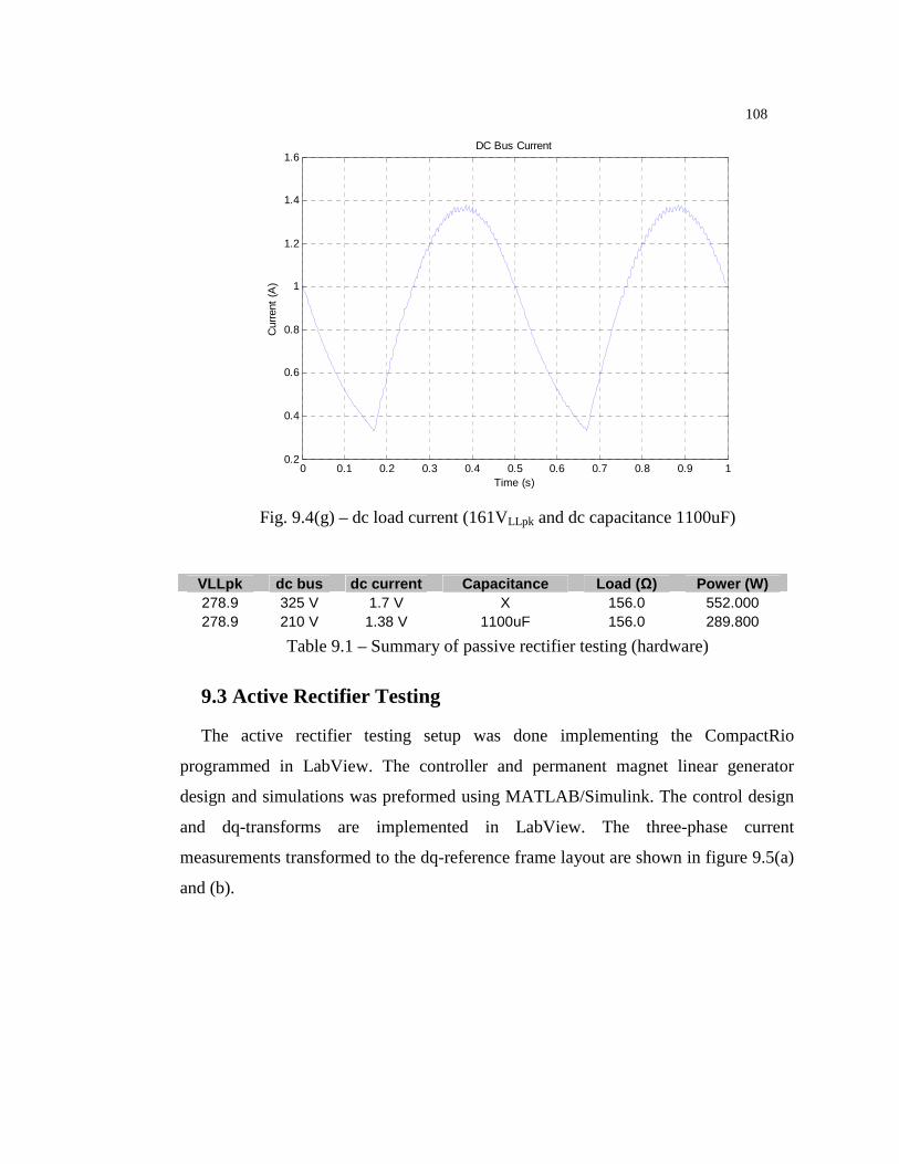
108
0 0.1 0.2 0.3 0.4 0.5 0.6 0.7 0.8 0.9 10.2
0.4
0.6
0.8
1
1.2
1.4
1.6DC Bus Current
Time (s)
Cur
rent
(A
)
Fig. 9.4(g) – dc load current (161VLLpk and dc capacitance 1100uF)
VLLpk dc bus dc current Capacitance Load (Ω) Power (W) 278.9 325 V 1.7 V X 156.0 552.000 278.9 210 V 1.38 V 1100uF 156.0 289.800
Table 9.1 – Summary of passive rectifier testing (hardware)
9.3 Active Rectifier Testing
The active rectifier testing setup was done implementing the CompactRio
programmed in LabView. The controller and permanent magnet linear generator
design and simulations was preformed using MATLAB/Simulink. The control design
and dq-transforms are implemented in LabView. The three-phase current
measurements transformed to the dq-reference frame layout are shown in figure 9.5(a)
and (b).

109
Fig. 9.5(a) – Three-phase to dq-reference frame
Fig. 9.5(b) – dq-reference frame to three-phase
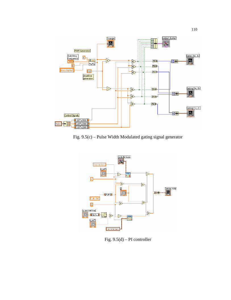
110
Fig. 9.5(c) – Pulse Width Modulated gating signal generator
Fig. 9.5(d) – PI controller

111
The “Controller Gains” block is a LabView graphical controller that accepts
proportional gain, integrator time and derivative time values. Integrator time is defined
as 1/Ki and the derivative term is 1/Kd, however this is omitted from our controller.
Hardware testing with the CompactRIO was not completely successful due to a
number of real-time controller issues. The timing of the real-time controller and the
FPGA board would lose connection with the end-user GUI if a set loop interval was
set on the FPGA. In order for the controller to properly run, a set loop interval needs to
be set otherwise the CompactRIO will compute the math based on an arbitrary speed.
For our controller, the loop needs to operate at 50 kHz (20us) or faster to generate the
appropriate PWM triangle wave. While programming the FPGA and real-time
controller, triangle wave generation was severely aliased resulting in unusable PWM
signals.

112
10 CONCLUSION
Modeling of the permanent magnet linear generator was done using dq-flux
equations and simulated in Simulink. An ideal model of the generator was also
developed to provide a baseline for simulation comparisons. A current controller was
derived from the PMLG machine equations and designed for our generator
specifications. Various simulations were performed with the ideal, dynamic and
average switching model to verify the controller design. A three-phase active rectifier
was designed with protective snubbers and used as a platform to test the controller
topology and configuration. A dc-dc converter is used to maintain the dc bus voltage
controlled by a hysteretic controller. The dc-dc converter dissipates power into a
resistive load bank.
Hardware selection of the IGBT modules and drive boards was specified to
ensure reliability, minimize size, maximize power handling capabilities, and allow
implementation with the real-time controller. A three-phase 120kVA fully
programmable source was used to generate a variable-voltage fixed frequency output.
The control signals were provided with the CompactRIO NI-9012 real-time controller
with digital output module. All transforms and controller designs were converted into
LabView code for compilation to the CompactRIO. During testing, the CompactRIO
had problems acquiring data and generating correct triangle waves for the PWM
generation. The timing issues, clock speeds and data acquisition on the real-time
controller were the source of highly aliased and unusable signals that could not be
used for controlling the IGBT gating signals. Hardware testing concluded with diode
testing with and without dc bus capacitance.
Future work would include correcting the CompactRIO timing and clock
issues to effectively run the compiled controller. An alternative would be a specific
real-time controller, such as dspace or Opal-RT real-time controller designed for HIL
(Hardware-In-Loop) systems. Lab testing with a 1kW linear generator on the designed

113
Linear Test Bed at Oregon State University would provide opportunity for controller
verification.

114
Bibliography
[1] Sorensen, Robert M. Basic Coastal Engineering. New York: Chapman Hall, 1997
[2] Brooking, P.R.M., and M.A. Mueller. “Power conditioning of the output from a
linear vernier hybrid permanent magnet generator use in direct drive wave
energy converters.” IEE Proc.-Gener. Transm. Distrib Vol. 152, No. 5 (2005):
673-681
[3] Mohan, Ned. Advanced Electric Drives. Minneapolis: MNPERE, 2001
[4] PowerEx Online References, Reverse Recovery Characteristics.
http://www.pwrx.com/pwrx/app/Ratings-12-13.pdf
[5] Mohan, Ned, Tore M. Undeland, and William P. Robbins. Power Electronics:
Converts, Applications, and Design. New Jersey: Wiley, 2003
[6] Gieras, Jacek F. and Zbigniew J. Piech. Linear Synchronous Motors:
Transportation and Automation Systems. Boca Raton: CRC Press, 2000
[7] Rashid, Muhammad. Power Electronics Handbook. San Diego: Academic Press,
2001.
[8] Kuo, Benjamin C, and Farid Golnaraghi. Automatic Control Systems. New Jersey:
Wiley, 2003.
[9] Forsyth, A.J. and S.V. Mollow. “Modelling and control of DC-DC converts”,
Power Engineering Journal. October 1998: 229-236
[10] Schacher, A.A. “Novel Control Design for a Point Absorber Wave Energy
Converter.”, Thesis for Masters of Science, Oregon State University. June:
2007
[11] Ang, Simon S. Power Switching Converters. New York: Marcel Dekker. Inc.
1995

115
Appendices