norwegian university of science and technology tet4190 ... reports/group 3 pv... · norwegian...
TRANSCRIPT
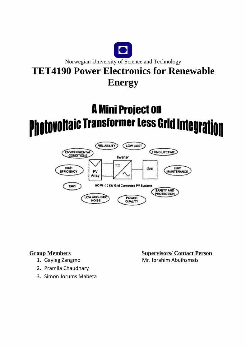
Norwegian University of Science and Technology
TET4190 Power Electronics for Renewable
Energy
Group Members Supervisors/ Contact Person
1. Gayleg Zangmo Mr. Ibrahim Abuihsmais
2. Pramila Chaudhary
3. Simon Jorums Mabeta

1

2
ACKNOWLEDGEMENT
This page is dedicated to individuals without whom the timely completion of the project
would not have been possible.
Our sincerest appreciation is extended to the respected Professor Tore M. Undeland and our
project supervisor Mr. Ibrahim Abuihsmais for their valuable suggestions and time. The
platform fed by them to conduct the project that realizes the implementation of knowledge
gained during the course of study is very precious. The relevant information provided by our
project supervisor was very helpful. We would like to show our utmost gratitude to the entire
Department of Electrical Engineering faculty and staff for all the support and encouragement
provided throughout the project duration.
We would like to thank Ms. Subhadra Tiwari for providing necessary materials for the project
and guiding us whenever needed. We also share our gratitude to our Teaching assistant Mr.
Sverre Skalleberg Gjerde for providing us the basic guidelines to use the simulation software
called PSCAD®. We are also thankful to other teaching and student assistants for their
support and help during the project duration.
We are deeply indebted to our senior students and fellow colleagues. Their comments and
contributions were a valuable input in to this project.
Last but not least, we would like to thank our families back at home for providing us moral
support and words of encouragement.
Project Members
Gayleg Zangmo
Pramila Chaudhary
Simon Jorums Mabeta

3
DEDICATION
TO
PEOPLE LIVING IN RURAL AREAS WHO DO NOT HAVE ACCESS TO
ELECTRICITY

4
Table of Contents
ABSTRACT ............................................................................................................................... 6
1. PROJECT OBJECTIVE ......................................................................................................... 7
2. PROJECT SCOPE OF WORK .............................................................................................. 7
3. INTRODUCTION .................................................................................................................. 7
4. BENEFITS OF PV SYSTEMS .............................................................................................. 7
5. PV APPLICATIONS ............................................................................................................. 8
5.1 Off-Grid PV system (Standalone PV system) .................................................................. 8
5.2. Hybrid Systems ............................................................................................................... 8
5.3 Grid-connected PV systems. ............................................................................................ 8
6. Grid connected Transformer-less Topologies ........................................................................ 9
6.1 Advantages and disadvantages ......................................................................................... 9
6.2 INVESTIGATED TOPOLOGIES ................................................................................... 9
6.2.1 HALF BRIDGE (HB) INVERTER ........................................................................... 9
6.2.2 Neutral Point Diode Clamped Inverter .................................................................... 10
6.2.3 FULL BRIDGE INVERTER .................................................................................. 10
6.2.4 HERIC TOPOLOGY .............................................................................................. 11
6.2.5 H5 TOPOLOGY ..................................................................................................... 11
7. SELECTION SCHEME OF TOPOLOGY FOR SIMULATION ........................................ 11
8. SIMULATION OF HERIC TOPOLOGY. .......................................................................... 12
9. RESULTS ............................................................................................................................. 14
10. DISCUSSION .................................................................................................................... 17
11. CONCLUSION .................................................................................................................. 18
12. References: ......................................................................................................................... 19
APPENDIX A: GOVERNING STANDARDS FOR PV INVERTER INSTALLATIONS ... 20
13. APPENDIX B: EXTRA POWER ELECTRONICS THEORY ......................................... 21
14. APPENDIX C: PSCAD® .................................................................................................. 22
15. APPENDIX D: PHOTOVOLTAIC SYSTEMS- Pictures. ................................................ 23
16. Appendix E: FURTHER INFORMATION ON PHOTOVOLTAIC SYSTEMS .............. 24

5
List of Acronyms 1. PV - Photovoltaic 2. AC - Alternating current 3. DC - Direct current 4. I - Current 5. V - Voltage 6. MPPT - Maximum Power Point Trackers 7. VSI - Voltage Source Inverters 8. FB - Full Bridge 9. HB - Half Bridge 10. D - Diodes 11. S - Power switch 12. PWM - Pulse Width Modulation 13. C - Capacitance 14. HERIC - Highly Efficient Reliable Inverter Concept. 15. PSCAD® - Power system computer aided design 16. THD - Total Harmonic Distortion 17. PF - Power Factor level 18. L - Inductance

6
ABSTRACT
Renewable energy sources are getting more and more widespread mainly due to the fact
that they are environmentally friendly. The reduced prices of Photovoltaic (PV) system
components and technological developments of power electronics have also motivated
the harnessing of renewable energy. Furthermore, renewable energy is independent of
limited fossil and nuclear fuels and thus it has the potential to be a sustainable energy
source for the future.
There is a strong trend in PV inverter technology to use transformer-less grid-connected
topologies. Transformer-less topologies eliminate the Line Frequency Transformer from
grid-connected PV systems. This results in reduced cost, physical size and weight of the
inverter. The other advantage is an increase in the overall power efficiency and
improved power factor at light loads.
The elimination of the transformer, however, creates challenges which the PV system
has to mitigate. Among these challenges is the need to provide galvanic isolation between
the PV generator and the connected grid. For other inverters, the galvanic isolation is
provided by the transformer. In these conditions, dangerous leakage currents (common-
mode currents) can appear through the stray capacitance between the PV array and the
ground. The
The other challenge introduced by transformer-less topologies, is the danger of direct
current (dc) injection in to the grid. Dc in an ac system causes saturation of distribution
transformers in the network and also affects the accuracy of Instrument transformers
and energy meters.
The choice of a transformer-less topology is thus critical in ensuring that the undesirable
operational effects are minimized to acceptable levels while achieving the benefits of
using the topology as outlined earlier.

7
1. PROJECT OBJECTIVE
The prime objective of this project is to investigate various transformer-less topologies for
modern PV application.
2. PROJECT SCOPE OF WORK
The scope of work included the following activities:
Study of background theory on PV components and electronic components.
Theoretical comparison of various inverter topologies and choice of one for further
investigation through software simulation.
Familiarization of PSCAD® simulation software.
Building up of the selected topology circuit for simulation.
Simulation of circuit and results analysis
Report write-up
3. INTRODUCTION
A PV system consists of various components which include solar panels, the inverter, the
filter elements and storage elements. Information was researched on the various components
of the PV inverter systems starting from the principle of operation of a solar cell, PV module
characteristics, components of PV modules and their manufacture, the optimization of PV
input-source through the use of Maximum Power Point Trackers (MPPT) as well as
associated components such as storage devices like batteries. Detailed documentation of this
is in Appendix E.
4. BENEFITS OF PV SYSTEMS
PV power systems offer many unique benefits above and beyond simple energy delivery.
These are as follows:
Social benefits in terms of job creation, energy independence and rural development.
No noise production, harmful emissions or polluting gases compared to other power
generating source which result in smoke creation, gases which cause acid rain, pollute
water and pollute the air
PV modules can be recycled and therefore the materials used in the production process
(silicon, glass, aluminium, etc.) can be reused. Recycling is not only beneficial for the
environment but also for helping to reduce the energy needed to produce those
materials and therefore the cost of fabrication.
PV requires minimal maintenance. Solar modules are almost maintenance free and
offer easy installation. PV systems are extremely safe and highly reliable. The
estimated lifetime of a PV module is 30 years
PV energy pay-back time is short and constantly decreasing. This means that the time
required for a PV module to produce as much energy as it would need to be
manufactured is very short.

8
5. PV APPLICATIONS
There are three types of PV systems.
5.1 Off-Grid PV system (Standalone PV system)
Where no mains electricity is available, the system is connected to a battery via a charge
controller. An inverter can be used to provide AC power, enabling the use of standard
electrical appliances. Typical off-grid applications are used to bring access to electricity to
remote areas (mountain huts, developing countries). Rural electrification means either a small
solar home system covering basic electricity needs in a single household, or large solar mini-
grids, which provide enough power for several homes.
Uses for solar electricity for remote applications are very frequent in the telecommunications
field, especially to link remote rural areas to the rest of the country. Repeater stations for
mobile telephones powered by PV also have a large potential. Other applications include
traffic signals, marine navigation aids, security phones, remote lighting, highway signs and
waste water treatment plants. These applications are cost competitive today as they enable
power to be brought to areas far from electricity mains, avoiding the high cost of installing
cabled networks.
Off-grid applications are often the most suitable option for supplying electricity in dispersed
communities or at great distances from the grid. A picture of this system is given in Appendix
5.2. Hybrid Systems
A PV system can be combined with another source of power-a biomass generator, a wind
turbine or diesel generator- to ensure a consistent supply of electricity. A hybrid can be grid-
connected, stand-alone or grid-support. A picture of this system is given in Appendix
5.3 Grid-connected PV systems.
These PV systems are grid-connected, produce large quantities of photovoltaic electricity in a
single point. The size of PV systems ranges from several hundred kilowatts to several
megawatts. Some of these applications are located on large industrial buildings such as airport
terminals or railway stations.
Grid-connected applications, currently the biggest market segment, are expected to remain so
for the foreseeable future. The substantial benefit of the grid-connected domestic market is the
control which PV systems allow the consumer over their power supply. Not only is electricity
generated at the point of demand, avoiding grid losses of electricity, but the consumer is
effectively is effectively transformed into the operator of his or her own power station.
There are two main topology groups used in case of grid connected PV systems and they are
a) With galvanic isolation – Galvanic isolation can be done on the DC side, in the form of a
high frequency DC-DC transformer or on the grid side in the form of a big-bulky AC
transformer.
b) Without galvanic isolation- Here, the transformer is omitted and is called as transformer-
less topology.

9
6. Grid connected Transformer-less Topologies
6.1 Advantages and disadvantages
The advantages of the Transformer less topologies are as follows:
a) Reduced weight, size and volume of the PV systems.
b) Absence of the transformer means reduced transformer losses and thus improved
efficiency of the system by 1-2%.
c) no inductive reactance contribution from the transformer, thus improved power factor
for low loading
d) reduced cost of the PV application since the transformer is eliminated
The absence of high or low frequency transformer, however, presents other challenges which
the different topologies of inverters have to address. Among these are the following:
a) The introduction of a leakage current between the output and input due to lack of
galvanic isolation
b) The change of voltage amplitude of the input to suit the requirements of the output or
grid.
c) The surface of the PV array forms a capacitor, with respect to ground, which is the
energized by the fluctuating potential. A person connected to ground and touching the
PV array may conduct the capacitive current to ground, causing an electrical hazard to
the person involved.
d) The voltage fluctuations generate electric and magnetic fields around the PV array
(electromagnetic interference).
A background research was done on the following topologies:
6.2 INVESTIGATED TOPOLOGIES
Considering the applications of PV systems and also due to limited time, only single phase
topologies were investigated. These are as follows:
6.2.1 HALF BRIDGE (HB) INVERTER
This topology uses one leg of two power switches, S1 and S2, for Pulse Width Modulation
(PWM) of an input dc and two anti-parallel diodes. It also has a capacitor divider C1 and C2
which splits the output current and eliminates the dc component in steady state operation of
the inverter. The circuit diagram is shown in figure 1 below.
Figure 1: Half-bridge Inverter

10
It is a simple circuit with few switches and thus results in lower conduction losses. However,
it requires a higher input voltage which consequently increases the rating of the inverter
components.
6.2.2 Neutral Point Diode Clamped Inverter
The topology is based on the HB circuit in figure 4 but it has extra two power switches and
diodes (D5 and D6) as shown in Figure 2. For the positive current half-wave switches S1 and
S2 are used and the negative half wave is generated by the PWM of S3 and S4. Turning S2
and S3 ON generates the zero output voltage.
Figure 2: Neutral Point Diode Clamped Inverter
6.2.3 FULL BRIDGE INVERTER
Figure 3: Full Bridge Inverter
The circuit is as shown in figure 3 above. It consists of two pairs of two switching power
devices in series with anti-paralleled diodes. It can be used to generate ac voltage using PWM
of the input with either Bipolar or Unipolar switching scheme.
The switching schemes are explained in Appendix B. It has an advantage over the Half
Bridge in that, for the same input power, the output current and switch currents are half those
of the half bridge.
However, it disadvantage is the flow free wheeling current of reactive power through the anti-
parallel diodes to the dc side resulting in additional losses. The dc input in to ac is limited by
the double inductor use in the circuit.

11
6.2.4 HERIC TOPOLOGY
Figure 4: HERIC Topology
Highly Efficient and Reliable Inverter Concept( HERIC) topology is based on a Full Bridge
circuit with each group of power switches operated at high switching frequency during one
half-wave of the output voltage.
The circuit has an additional branch of switches, each one active during half-wave period of
the grid wave form. This bridge provides a path for the free wheeling current, eliminating the
circulation of reactive power and increasing the efficiency and voltage.
The main draw back in this topology is the increased number of semiconductors.
6.2.5 H5 TOPOLOGY
Figure 5: H5 Topology
This circuit is also based on the Full Bridge with the same operations of the bridge switches.
It has an extra power switch and anti-paralleled diode on the dc side of the inverter to
electrically decouple the ac from the dc side during free wheeling period.
Its main draw back is the higher conduction losses due to the series associated of three
switches during the active phase.
7. SELECTION SCHEME OF TOPOLOGY FOR SIMULATION
Due to the limited amount of time, only the above 5 topologies were extensively researched.
However, other variations exist and even new ones have been proposed with different
advantages. The various characteristics are summarized in the table below:
12
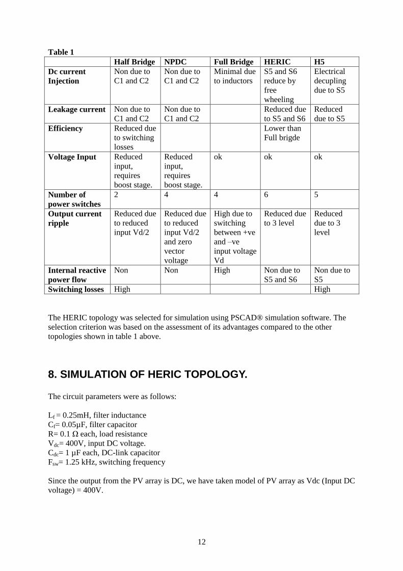
Table 1
Half Bridge NPDC Full Bridge HERIC H5
Dc current
Injection
Non due to
C1 and C2
Non due to
C1 and C2
Minimal due
to inductors
S5 and S6
reduce by
free
wheeling
Electrical
decupling
due to S5
Leakage current Non due to
C1 and C2
Non due to
C1 and C2
Reduced due
to S5 and S6
Reduced
due to S5
Efficiency Reduced due
to switching
losses
Lower than
Full brigde
Voltage Input Reduced
input,
requires
boost stage.
Reduced
input,
requires
boost stage.
ok ok ok
Number of
power switches
2 4 4 6 5
Output current
ripple
Reduced due
to reduced
input Vd/2
Reduced due
to reduced
input Vd/2
and zero
vector
voltage
High due to
switching
between +ve
and –ve
input voltage
Vd
Reduced due
to 3 level
Reduced
due to 3
level
Internal reactive
power flow
Non Non High Non due to
S5 and S6
Non due to
S5
Switching losses High High
The HERIC topology was selected for simulation using PSCAD® simulation software. The
selection criterion was based on the assessment of its advantages compared to the other
topologies shown in table 1 above.
8. SIMULATION OF HERIC TOPOLOGY.
The circuit parameters were as follows:
Lf = 0.25mH, filter inductance
Cf= 0.05µF, filter capacitor
R= 0.1 Ω each, load resistance
Vdc= 400V, input DC voltage.
Cdc= 1 µF each, DC-link capacitor
Fsw= 1.25 kHz, switching frequency
Since the output from the PV array is DC, we have taken model of PV array as Vdc (Input DC
voltage) = 400V.
13
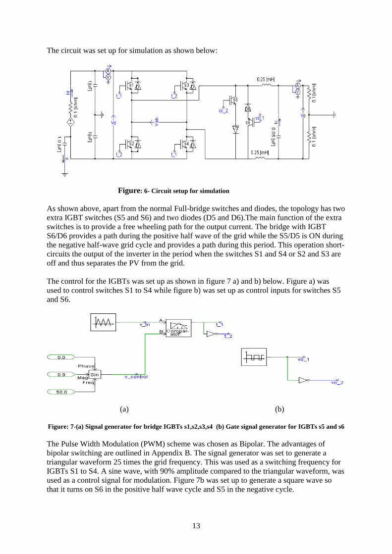
The circuit was set up for simulation as shown below:
Figure: 6- Circuit setup for simulation
As shown above, apart from the normal Full-bridge switches and diodes, the topology has two
extra IGBT switches (S5 and S6) and two diodes (D5 and D6).The main function of the extra
switches is to provide a free wheeling path for the output current. The bridge with IGBT
S6/D6 provides a path during the positive half wave of the grid while the S5/D5 is ON during
the negative half-wave grid cycle and provides a path during this period. This operation short-
circuits the output of the inverter in the period when the switches S1 and S4 or S2 and S3 are
off and thus separates the PV from the grid.
The control for the IGBTs was set up as shown in figure 7 a) and b) below. Figure a) was
used to control switches S1 to S4 while figure b) was set up as control inputs for switches S5
and S6.
(a) (b)
Figure: 7-(a) Signal generator for bridge IGBTs s1,s2,s3,s4 (b) Gate signal generator for IGBTs s5 and s6
The Pulse Width Modulation (PWM) scheme was chosen as Bipolar. The advantages of
bipolar switching are outlined in Appendix B. The signal generator was set to generate a
triangular waveform 25 times the grid frequency. This was used as a switching frequency for
IGBTs S1 to S4. A sine wave, with 90% amplitude compared to the triangular waveform, was
used as a control signal for modulation. Figure 7b was set up to generate a square wave so
that it turns on S6 in the positive half wave cycle and S5 in the negative cycle.

14
9. RESULTS
Output channels were set up at various points on the circuit in figure 9 and the waveforms
were captured as shown in the figures 8 to 15 below. The list of waveforms obtained is as
follows:
1. Output Voltage – Figure 8
2. Output Current with leakage current – Figure 9
3. Input and Output Power – Figure 10
4. Bridge Output Voltage – Figure 11
5. Control Signals – Figure 12
6. Leakage Current – Figure 13
7. Input DC Voltage Waveform – Figure 14
8. Input DC Current Waveform – Figure 15
Figure 8 – Waveform of Output Voltage Vo across purely resistive load
Figure 9 – Waveform of Output Current Io and leakage current II

15
Figure 10- Waveform of Input Power Pi and Output Power Po
Figure 11- Waveform of output voltage of inverter Vab
Figure 12- Waveform of sinusoidal Control voltage v control and gating signal for switch s5

16
Figure 13- Waveform of leakage current II
Figure 14- Waveform of Input DC voltage Vd
Figure 15- Waveform of Input DC current Id
17
10. DISCUSSION
The activities that were carried out during simulation of the HERIC topology can be
summarized as follows:
PSCAD familiarization. Different circuit configurations were set up to confirm or
understand the operation of various circuit components. Some of the components
investigated included the operation of IGBT and BJT switches, signal generators,
capacitors and inductors and dc source generator, Multimeters and grounding.
Understanding the behavior of the inverter. The current and voltage waveforms were
measured through the conversion stage from the output of the dc source, the input in to
the H Bridge, the output of the H Bridge and finally from the output of the filter. A
range of values for load resistance, filter inductance, dc and filter capacitor, source
resistance was investigated.
The effect of frequency modulation as well as amplitude modulation on the output
waveforms. The switching frequency was varied from 1.25 kHz to 8kHz while
amplitude was varied from 40% to 100%
Obtaining sinusoidal output current and voltage waveforms.
Minimizing the leakage current. The leakage capacitance of a PV panel was modeled
as a 1 micro Farad capacitance connected between the negative terminal of the dc
source and ground. This current was measured for different values of circuit
components to simulate different conditions. Instead of using dc input split capacitors
and filter inductor components, simulations were also done using a capacitor or
inductor as one whole component.
Isolation of DC side from AC side using switches S5 and S6. The circuit was
simulated without the free wheeling arms and compared with the HERIC topology.
Increasing input/output power efficiency.

18
11. CONCLUSION
From the investigations carried out on this topology, the following conclusions can be drawn:
a) Leakage current can be minimized to the lowest acceptable levels using a split input
dc capacitor and split filter inductor components. It must be ensured that the values of
these dual components are equal to avoid imbalance as the imbalance leads to a higher
leakage current. Having taken the aforesaid in to consideration, the measured results
for leakage current were minimal as compared to output current as seen in figures 9
and 13.
b) The dc ac isolation is possible using free wheeling bridge. However, it was observed
that this was achieved at the expense of power efficiency. Power measurements are as
shown in figure 10.
c) Sinusoidal generation of current and voltage waveforms is achievable from varying
the values of filter components as well as the frequency modulation from the control
signals.
d) A specific load requires a specific combination of filter element values to achieve
optimum operation.

19
12. References:
1. Mr. Roberto Gonzalez, Jesus Lopez, Pablo Sanchis, Luis Marroya, Transformersless Inverter for Single-Phase Photovoltaic Systems, IEEE, 2007.
2. J.M. A. Myrzik, and M. Calais, String and Module Integrated inverters for single-phase grid connected photovoltaic systems- A review, IEEE, 2003.
3. Tamas Kerekes, Remus Teodorescu, Pedro Rodriguez, Gerardo Vazquez, Emiliano Aldabas, A new high-efficiency single phase transformerless PV inverter topology, IEEE, 2009.
4. Martina Calais and Vassilios G. Agelidis, Multilevel Converters for Single-phase Grid
Connected Photovoltaic Systems- An Overview, IEEE, 1998 5. Arthouros Zervous, Christine Lins, Renewable Energy in Europe –Markets, trends and
technologies, 2nd
Edition, EREC, 2010
6. Mohan, Undeland, Robbins, Power Electronics for converters, applications and design, Third
Edition, 2003.
7. Eugenio Gubia, Pablo Sanchis, Alfredo Ursua, Jesus Lopez and Luis Marroyo, Ground
Currents in Single-phase Transformerless Photovoltaic Systems, published in Wiley
Interscience, May 2007.
8. Martina Calais, Johana Myrzik, Ted Spooner, Vassilios G. Agelidis, Inverters for Single-
Phase Grid Connected Photovoltaic Systems- An Overview, IEEE, 2002.
9. Fritz Schimpf, Lars E. Norum, Grid Connected Converters for Photovoltaic, State of the Art,
Ideas for Improvement of Transformerless Inverters, Nordic Workshop on Power and
Industrial Electronics, June 9-11,2008.
10. T. Kerekes, R. Teodorescu, U. Borup, Transformerless Photovoltaic Inverters Connected to
the Grid, IEEE, 2007.
11. Martina Calais, Andrew Ruscoe, Michael Dymond, Transformerless PV Inverter Issues
Revisited- Are Australian Standards Adequate, Solar09, The 47th ANZSEs Annual
Conferences 29 September-2 October 2009.
12. G. Ofualagba, Photovoltaic Technology, Applications and Market, IEEE, 2008.
13. Denizar C. Martins and Kleber C.A. de Souza, A Single-Phase Grid-Connected PV system
with Active Power Filter, International Journal of circuits, systems and signal processing,
Issue 1, Volume 2, 2008.
14. Eduardo Roman, Ricardo Alonso, Pedro Ibanez, Intelligent PV Module for Grid-Connected
PV systems, IEEE, 2006
15. Engin Ozdemir, Fatih Kavaslar, A new Multifunctional Power Converter for Grid Connected
Residential Photovoltaic Applications, IEEE, 2009.
16. R.K. Nema, Savita Nema and Gayatri Agnihotri, Computer Simulation Based Study of
Photovoltaic Cells/Modules and their Experimental Verification International Journal of
Recent Trends in Engineering Vol 1, No.3, May, 2009.
20
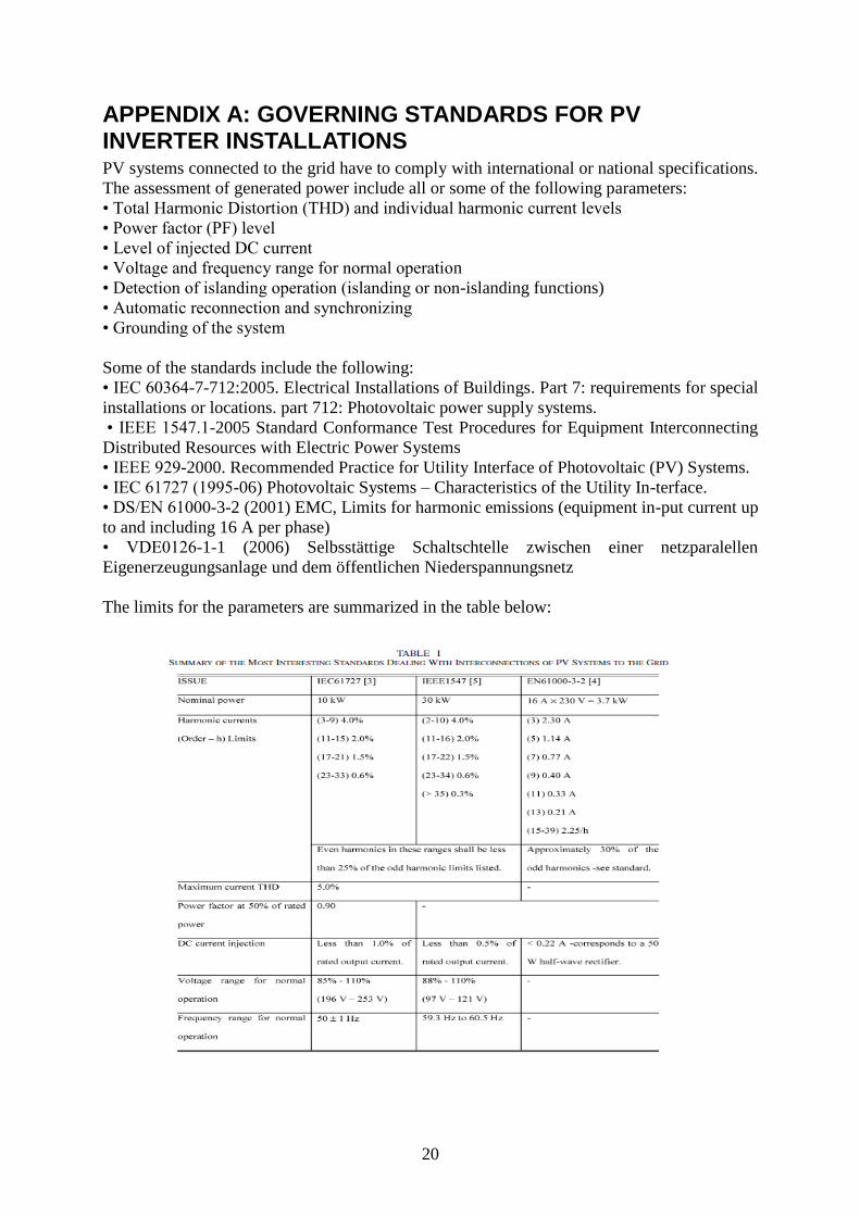
APPENDIX A: GOVERNING STANDARDS FOR PV INVERTER INSTALLATIONS PV systems connected to the grid have to comply with international or national specifications.
The assessment of generated power include all or some of the following parameters:
• Total Harmonic Distortion (THD) and individual harmonic current levels
• Power factor (PF) level
• Level of injected DC current
• Voltage and frequency range for normal operation
• Detection of islanding operation (islanding or non-islanding functions)
• Automatic reconnection and synchronizing
• Grounding of the system
Some of the standards include the following:
• IEC 60364-7-712:2005. Electrical Installations of Buildings. Part 7: requirements for special
installations or locations. part 712: Photovoltaic power supply systems.
• IEEE 1547.1-2005 Standard Conformance Test Procedures for Equipment Interconnecting
Distributed Resources with Electric Power Systems
• IEEE 929-2000. Recommended Practice for Utility Interface of Photovoltaic (PV) Systems.
• IEC 61727 (1995-06) Photovoltaic Systems – Characteristics of the Utility In-terface.
• DS/EN 61000-3-2 (2001) EMC, Limits for harmonic emissions (equipment in-put current up
to and including 16 A per phase)
• VDE0126-1-1 (2006) Selbsstättige Schaltschtelle zwischen einer netzparalellen
Eigenerzeugungsanlage und dem öffentlichen Niederspannungsnetz
The limits for the parameters are summarized in the table below:

21
13. APPENDIX B: EXTRA POWER ELECTRONICS THEORY 1. DIRECT CURRENT INJECTION
Direct Current dc injection in to the grid causes the saturation of the transformers in the
distribution network. While safety requirements in transformer-less systems can be met by
means of external elements, leakage currents and the injection of dc into the grid must be
guaranteed topologically or by the inverter’s control system. This paper proposes a new high-
efficiency topology for transformer-less systems, which does not generate common-mode
currents and topologically guarantees that no dc is injected into the grid. The proposed
topology has been verified in a 5-kW prototype with satisfactory results.
Table 2: Limits of DC current injection of different standards
STANDARD IEC 61727 IEEE1547
IEEE929-2000
EN61000-3-2 VDE0126-1-1
DC CURRENT
INJECTION
LIMIT
<1% of rated
output current
<0.5% of rated
output current
<0.22A for a
50W half-wave
rectifier
<1A
2 GALVANIC CONNECTION
The galvanic connection between the grid and the PV array results in the appearance of a
common-mode resonant circuit consisting, on the stray capacitance, of the PV generator to
ground and the filtering elements. If the common-mode voltage generated by the inverter
includes frequencies close to that of the circuit’s resonance, large common-mode currents will
appear. These common-mode currents might cause severe (conducted and radiated)
electromagnetic interferences, grid current distortion, and additional losses in the system.
This may also cause safety hazards in the event of ground faults. In addition, the
circulation of leakage currents (common-mode currents) through the stray capacitance
between the PV array and the ground would be enabled. The seriousness of these effects
has been an area of concern and controversial discussion over the past years. Meanwhile
different studies show that the impact of PV systems with transformer less inverters on
electromagnetic interference is usually negligible and does not pose a hazard. However, with
respect to capacitive currents certain recommendations on inverter and PV system design
should be followed to prevent dangerous current levels (above ~10mA)
A ground fault detector is a simple but reliable device that disconnects the inverter upon the
detection of an isolation fault in the installation
It should be noted however, that in some countries like the UK, galvanic isolation is a
requirement and as such the transformer-less topology cannot be employed.
3. UNIPOLAR SWITCHING
One of the main associated advantages of implementing a unipolar switching scheme as
opposed to a bipolar scheme is that the switching losses are significantly reduced because the
associated voltage drop from switching from one state to another is halved. One of the
downsides of implementing a unipolar switching scheme however is that there are higher
associated harmonic content in the output current around the zero crossing (particularly at
lower power levels.
4 BIPOLAR PWM
Bipolar modulation causes large current ripple and high switching losses, reducing the overall
efficiency of the inverter.

22
14. APPENDIX C: PSCAD®
PSCAD® stands for power system computer aided design.
PSCAD® is a fast, accurate, and easy-to-use power system simulation software for the design
and verification of all types of power systems. PSCAD® is also known as
PSCAD®/EMTDC™ because EMTDC™ is the simulation engine, which is now the integral
part of PSCAD® graphical user interface.
PSCAD® is most suitable for simulating time domain instantaneous responses, also known
as electromagnetic transients or instantaneous solutions, in both electrical and control
systems.
The PSCAD® graphical user interface greatly enhances the power and usability of the
simulation environment. It allows the user to efficiently construct a circuit schematic, run a
simulation, analyze the results, and manage the data in a completely integrated graphical
environment. PSCAD® provides intuitive and interactive control input, meters, and online
plotting functions and graphs.
PSCAD® has been adopted worldwide by utilities, manufacturers, research & educational
institutions, and consultants as the premier tool for transient simulation. These people rely on
the extensive library of power and control system models, as well as, the accuracy and
reliability PSCAD® provides.

23
15. APPENDIX D: PHOTOVOLTAIC SYSTEMS- Pictures.
Fig. 9: Crystalline Silicon Solar Cell
Fig. 10:Stand-Alone Off-Grid PV System Schematic Fig.11: Hybrid Off-Grid PV System |
Schematic.
Fig. 12: Grid-connected PV system.

24
16. Appendix E: FURTHER INFORMATION ON PHOTOVOLTAIC SYSTEMS
Photovoltaic is a marriage of two words: ‘photo’ from Greek roots, meaning light and
‘voltaic’, from ‘volt’, which is the unit used to measure electric potential at a given point.
Photovoltaic (PV) systems use cells to convert solar radiation in to electricity.
3.1 Photovoltaic – The working principle
A photovoltaic cell is simply a p-n junction semiconductor device and acts like a diode in
absence of sunlight. The p-type and n-type semiconductors are formed by adding elements of
group V like Phosphorous and group III like Boron respectively to an intrinsic semiconductor.
The elements added are called impurities and the process is called doping.
Hence we can say that the semiconductors of p-type and n-type respectively have excess of
holes and electrons. When such layers are brought together then the excess charge carriers
start drifting towards the region of lower concentration leaving behind oppositely charged
carriers and during this process, they combine with each other to form depletion layer. This
process continues until the sufficient electric field to stop the further movement in the
junction is developed.
There is an energy band gap between the valence band and conduction band of a
semiconductor material. When the photons of light with energy greater than or equal to the
energy band gap of the semiconductor fall on the solar cells then the electrons get excited and
move to conduction band from the valence band, leaving behind holes in the valence band.
This results in the formation of electron-hole pair.
When a conductor is connected across the p-n layer to form an electric circuit with load then
current flows. This direct conversion of light energy into electrical energy is called
photovoltaic. The current thus generated is DC.
The following figure depicts the generation of electron–hole pair.
Fig. 1: Generation of electron- hole pair by photons
The solar cells are connected together to form a PV module. The PV modules are connected
electrically together in series parallel form to get desired voltage- current combination. Such
combination of the PV modules is called PV array. The current is directly related to the
surface area of the solar cell and the value of solar irradiance incident on it.

25
Fig. 2: characteristic of a PV module
The above figure shows the IV characteristic of a PV panel. Isc is the short circuit current, Voc
is the open circuit voltage, Vm and Im are the voltage and current at Maximum Power Point,
Pm is the maximum power. MPP is the point at which the output power is maximum.
Pm = Im*Vm
The figure below shows the temperature effect in IV (Current-Voltage) characteristic of a PV
panel. We can see that the short circuit current increases while the open circuit voltage
decreases when temperature of cell is increased. The reduction in latter parameter is more
than the increase in the former one so the net effect is the reduction in power produced.
Fig. 3: temperature effect in IV curve
2.2 Components of Photovoltaic systems:
The various components of photovoltaic systems are given below:
a) PV Modules:
The primary article of commerce in the PV market is the PV module. PV modules are rated
on the basis of the power delivered under Standard Testing Conditions (STC) of 1kW/M2 of
sunlight and a PV cell temperature of 25 degree Celcius (°C). Their output measured under
STC is expressed in terms of “peak Watt” or Wp nominal capacity.
Manufacture of PV modules
To make PV modules, PV manufacturers use crystalline silicon wafers or advanced thin film
technologies. In the former, single crystal silicon (single-Si), polycrystalline silicon (poly-Si)
or ribbon silicon (ribbon-Si) wafers are made into solar cells in production lines utilizing
processes and machinery typical of the silicon semiconductor industry. Solar cell
manufacturers then assemble the cells into modules or sell them to module manufacturers for
assembly. Most modules in the market are designed to deliver direct current (DC) at slightly
over 12 Volts (V). A typical crystalline silicon module consists of a series circuit of 36 cells,
encapsulated in a glass and plastic package for protection from the environment. This package
is framed and provided with an electrical connection enclosure, or junction box. Typical

26
conversion (solar energy to electrical energy) efficiencies for common crystalline silicon
modules are in the 11 to 15% range.
There are four advanced thin film technologies. Their names are derived from the active cell
materials: cadmium telluride (CdTe), copper indium diselendie( CIS), amorphous silicon (a-
Si) and thin film silicon( thin film-Si). Amorphous silicon is in commercial production while
the other three technologies are slowly reaching the market. A picture of a PV cell is given in
Appendix D.
b) Batteries
Batteries store electricity to provide energy on demand at night or on overcast days. Off-grid
PV systems make use of batteries which act as energy storage device. The most common
battery types are lead-calcium and lead antimony. Nickel-Cadmium batteries can also be used,
in particular when the battery is subject to a wide range of temperatures.
Batteries are characterized by their voltage, which for most applications is a multiples of 12
V, and their capacity, expressed in Ampere-hours (Ah). For example a 50Ah, 48V battery will
store 50 x 48=2,400 Wh of electricity under nominal conditions.
c) Voltage regulator or charge controller
It is an essential part of nearly all standalone PV systems that charge batteries. Its purpose is
to keep your batteries properly fed and safe for the long term. It prevents block reverse current
and prevents battery from getting overcharged. It will also prevent battery overdischarge,
protect from electrical overload, and /or display battery status and flow of power.
d) Maximum Power Point trackers (MPPT) - Maintain the operating voltage of the array to
a value that maximizes array output.
e) Inverters - Convert the direct current (DC) output of the array or the battery into
alternating current (AC). These inverters are called voltage source inverters (VSIs).AC is
required by many appliances and motors. Inverter is also called as power conditioner.
f) Structure- required to mount or install the PV module and other components.