non-volatile memory technology: directions beyond floating ......©2013 micron technology, inc. | 2...
TRANSCRIPT

©2013 Micron Technology, Inc. All rights reserved. Products are warranted only to meet Micron’s production data sheet specifications. Information, products, and/or specifications are subject to change without notice. All information is provided on an “AS IS” basis without warranties of any kind. Dates are estimates only. Drawings are not to scale. Micron and the Micron logo are trademarks of Micron Technology, Inc. All other trademarks are the property of their respective owners.
1 ©2013 Micron Technology, Inc. |
Non-Volatile Memory Technology: Directions Beyond
Floating Gate Devices
Bob Gleixner and Chandra Mouli
Micron Technology

2 ©2013 Micron Technology, Inc. |
Two question to ask (for a new NVM)…
▶ What are the cost/performance characteristics required to add significant value in computing devices?
▶ For the leading emerging NVM’s, what materials improvements are needed to realize this value?
3 ©2013 Micron Technology, Inc. |
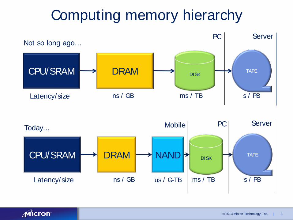
Computing memory hierarchy
CPU/SRAM DRAM DISK TAPE
ns / GB ms / TB s / PB
CPU/SRAM DRAM DISK TAPE
ns / GB ms / TB s / PB
NAND
us / G-TB
Not so long ago…
Today…
PC Server
PC Server Mobile
Latency/size
Latency/size

4 ©2013 Micron Technology, Inc. |
NOR
W R
NOR
Where could a new memory add value?
A. Fazio, IEDM 2009
Normalized Parameters
DRAM NAND HDD
Latency 1x ~500x ~100,000x
$/Bit 1x ~0.1x ~0.01x
NAND had a big “hole to fill” in 2009
What do the holes look like today?
More importantly, what does this look like in 3-5 years?
(Assumption – you find a niche to grow)
Latency NAND DISK DRAM
Bit/$ NAND DISK DRAM

5 ©2013 Micron Technology, Inc. |
Planar NAND is getting tough to scale…
G. Naso, ISSCC 2013 – 128Gb 20nm NAND Goda and Parat, IEDM 2012
Prall and Parat, IEDM 2010
Sigm
a
Threshold Voltage
Prall and Parat, IEDM 2010
3 bit/cell

6 ©2013 Micron Technology, Inc. |
…but continues to find solutions
www.cnet.com
www.samsung.com
Planar floating gate cell
Goda and Parat, IEDM 2012
16nm NAND announced
3D NAND
Goda, VLSI-TSA 2013

7 ©2013 Micron Technology, Inc. |
While DRAM continues to scale
Seon Yong Cha, IEDM short course, 2011

8 ©2013 Micron Technology, Inc. |
Main vector in DRAM/NAND: Cost reduction
Latency NAND DISK DRAM
Bit/$ NAND DISK DRAM
Latency NAND DISK DRAM
Bit/$ NAND DISK DRAM Today:
3 Years? :

9 ©2013 Micron Technology, Inc. |
Where can an emerging memory fit in?
Latency NAND DISK DRAM
Bit/$ NAND DISK DRAM SCM
(Storage class memory)
Latency NAND DISK DRAM
Bit/$ NAND DISK DRAM NVDRAM
(Non-Volatile DRAM)
Latency NAND DISK DRAM
Bit/$ NAND DISK DRAM
NAND REPLACEMENT (STORAGE)

10 ©2013 Micron Technology, Inc. |
Consider the “top 4” emerging memories
IEEE Solid-State Circuits Mag. Spring 2013
Technology Company Niche
RRAM Adesto EEPROM Replacement
MRAM EverspinUltra high Reliability
BBSRAM replacement
STRAM CrocusEmbeddedSecurity
FERAM TI Embedded
FERAM Ramtron Low Density – Power Meters
PCM SamsungMicron
NOR replacement-Wireless applications
Prall, IMW 2012

11 ©2013 Micron Technology, Inc. |
Memory “scorecard”
▶ Cost / bit
Small bit cell
Low programming energy
Multi-level or multi-layer
▶ Latency
Fast read (large signal +
memory window)
Fast / deterministic writes
Write endurance
Planar NAND
DRAM
Cost
Cell size 4F2 16nm
6F2 2x nm
Programming energy
Low (Refresh)
Multi-level / layer
1-3 BPC None
Latency
Fast read 10uS (page)
~10ns
Fast write 1mS (page)
~10ns
Endurance 1-100k >1e15

12 ©2013 Micron Technology, Inc. |
Phase Change Memory (PCM)
Page 12
▶ Storage mechanism
Amorphous/poly-crystal phase of chalcogenide alloy (Ge2Sb2Te5 – GST)
▶ Writing mechanism
Current-induced Joule heating
▶ Sensing signal
Resistance change of the GST
▶ Cell structure
1 transistor, 1 resistor (1T/1R)
Amorphous Crystalline
High resistivity Low resistivity
Amorphous Crystalline
High resistivity Low resistivity
I
V
I
V
Time
Temperature
Tx
Tm
Reset (amorphization)
Set (crystallization)
Time
Temperature
Tx
Tm
Reset (amorphization)
Set (crystallization)

13 ©2013 Micron Technology, Inc. |
History of PCM Silicon Development
2001 2003 2005 2007 2009 2011
M. Gill et al., ISSCC 2002
180nm
G. Casagrande et al., VLSI 2004
180nm
PCM cell
S. Lai and T. Lowrey, IEDM 2001
180nm
F. Pellizzer et al., VLSI 2006
90nm
Bedeschi et al., ISSCC 2008
90nm 128Mb (256Mb MLC)
G. Servalli, IEDM 2009
45nm
PCM array & chip
F. Pellizzer et al., VLSI 2004
180nm
C. Villa et al., ISSCC 2010 45nm 1Gb
Concept Demonstration
Technology Validation
Product Manufacturing

14 ©2013 Micron Technology, Inc. |
PCM Scorecard
Planar NAND
DRAM PCM
Cost Overall
Cell size 4F2 16nm
6F2 2x nm
4F2 20nm
Programming energy Low (Refresh) ~High I
Multi-level / layer 1-3 BPC None Level/Layer
Latency Overall
Fast read 10uS (page)
~10ns <100ns
Fast write 1mS (page)
~10ns >100ns
Endurance 1-100k >1e15 1e8

15 ©2013 Micron Technology, Inc. |
▶ Resistance drift (MLC)
▶ Thermal disturb
PCM Cell Challenges ▶ High programming current
▶ Programming speed to SET/crystallized state
Ielmini TED 2007
Russo TED 2008
Choi, ISSCC 2012
Sadeghipour, ITHERM 2006 Kang, IEDM 2011
20nm cell

16 ©2013 Micron Technology, Inc. |
RRAM RRAM Material Systems Switching mechanism Comments
RRAM-M(CBRAM)
Cu/GdOxAg/SiO2Ag/GeS
Metal Filament in Electrolyte Ion/Ioff ~ 1000
BipolarRRAM-Ox
Ti/HfOx, Ti/ZrOx
Oxygen vacancy filament in dielectric TiOx, ZrOx, TaOx etc,. Ion/Ioff ~ 10
RRAM-MVO Mixed Valence Oxides SrTiOx, PCMO etc,.
Uniform oxygen movement Ion/ Ioff ~10
TiN
Ti, Hf
W, TiN etc,.
Cu, Ag etc,.
+V -V
+V -V
H.Y.Lee etal, IEDM 2008
K.Aratani etal, IEDM 2008
Meyer etal, NVMTS 2008

17 ©2013 Micron Technology, Inc. |
RRAM Scorecard
Planar NAND
DRAM RRAM
Cost Overall
Cell size 4F2 16nm
6F2 2x nm
4F2 20nm
Programming energy Low (Refresh) Low - Med
Multi-level / layer 1-3 BPC None Level/Layer
Latency Overall
Fast read 10uS (page)
~10ns <100ns
Fast write 1mS (page)
~10ns ~10nS
Endurance 1-100k >1e15 1e8 ??

18 ©2013 Micron Technology, Inc. |
RRAM Cell Challenges
▶ Window for MLC
▶ Write current scalability?
Prall IMW 2012 – HfOx Aratani IEDM 2007 -- CBRAM
Write
Read
Chen IEDM 2012 – HfOx
▶ Noise

19 ©2013 Micron Technology, Inc. |
MRAM ▶ Fast switching could enable DRAM replacement
▶ But field / toggle MRAM cell too large STT-MRAM
Rizzo, IEEE Trans Mag 2013
MR4A16B Datasheet, www.everspin.com
20nm Ru .25Co/.8Pd * 14 .9 Ru 0.3 Co 0.25Co / .8 Pd * 4 0.8 Pt 0.25Co 0.3 Ta 0.8 CoFeB 0.5 Fe 0.9 MgO 0.8 CoFeB 2 Ta 5 RuCoFe Substrate
Sun, IEEE DRC 2011
Fixed layer MgO
Free layer
PMA Stack

20 ©2013 Micron Technology, Inc. |
STT-MRAM Scorecard
Planar NAND
DRAM STT-MRAM
Cost Overall
Cell size 4F2 16nm
6F2 2x nm
6F2
20nm
Programming energy Low (Refresh) Med I
Multi-level / layer 1-3 BPC None Layer
Latency Overall
Fast read 10uS (page)
~10ns <30ns
Fast write 1mS (page)
~10ns ~10ns
Endurance 1-100k >1e15 >1e15

21 ©2013 Micron Technology, Inc. |
STT-MRAM Cell Challenges ▶ Writing current vs. stability
▶ Operating window
▶ Tunnel junction reliability
Gallagher, ICSICT 2012 Slaughter, IEDM 2012
Slaughter, IEDM 2012
Ando, NVMTS 2011
Park, VLSI 2012

22 ©2013 Micron Technology, Inc. |
FERAM ▶ Stores “charge” in a
polarizable material
Typically PZT
▶ As with field/toggle MRAM, performance is similar to DRAM
Wouters, CREMSI Workshop 2004
http://www.cypress.com/

23 ©2013 Micron Technology, Inc. |
FERAM Scorecard
Planar NAND
DRAM FERAM
Cost Overall
Cell size 4F2 16nm
6F2 2x nm
>100nm
Programming energy Low (Refresh) Low
Multi-level / layer 1-3 BPC None Layer?
Latency Overall
Fast read 10uS (page) ~10ns ~10ns
Fast write 1mS (page)
~10ns ~10ns
Endurance 1-100k >1e15 >1e14

24 ©2013 Micron Technology, Inc. |
FERAM Cell Challenges
▶ Need to reduce cells size – limited by polarization / bitline cap ratio
▶ Considering cell / array architecture solutions
Takashima NVMTS 2011
Shiga JSSC 2010

25 ©2013 Micron Technology, Inc. |
Multi-Layer Memory
• Crossbar memory very attractive
▶ “Simple” structure and minimum cell size (4F2)
▶ Suitable for 3D stacking cell size (4/n)F2
▶ Array over circuitry better array efficiency
• The basic cell architecture requires a selector structure to be integrated in the BEOL
▶ Parasitic paths exist through neighboring cells
▶ Programming (and also reading) can perturb
the array
Vprog
0 V
Vprog/2
Vprog/2
Vprog/2 Vprog/2

26 ©2013 Micron Technology, Inc. |
A Wide Range of Material Choices
• Homojunctions polySi p/n junctions
• Heterojunctions p-CuO/n-InZnO • Schottky diode Ag/n-ZnO
• Chalcogenide Ovonic Threshold Switching (OTS) materials
• Mixed Ionic Electronic Conduction (MIEC) materials
Selector device options
For the selector structure several devices have been
proposed so far, none have been “proven”

27 ©2013 Micron Technology, Inc. |
Cross-Point Switch Requirements
▶ Very high forward bias current Greater than the switching current
▶ Low leakage through unselected cells Steep IV characteristic
▶ Bipolar operation may be required Necessary for bipolar RRAM
Cell Type
~20nm Cell Current
Current density
PCM 100uA 10 MA/cm2
RRAM 10uA 1 MA/cm2
Curr
ent
Voltage
1.E+00
1.E+01
1.E+02
1.E+03
1.E+04
1.E+05
0 2 4 6 8 10
Array size < ILRS(V) / ILRS (V/2)
Leakage per deselect cell (V/2 scheme)
Example for read Read current of selected cell
28 ©2013 Micron Technology, Inc. |
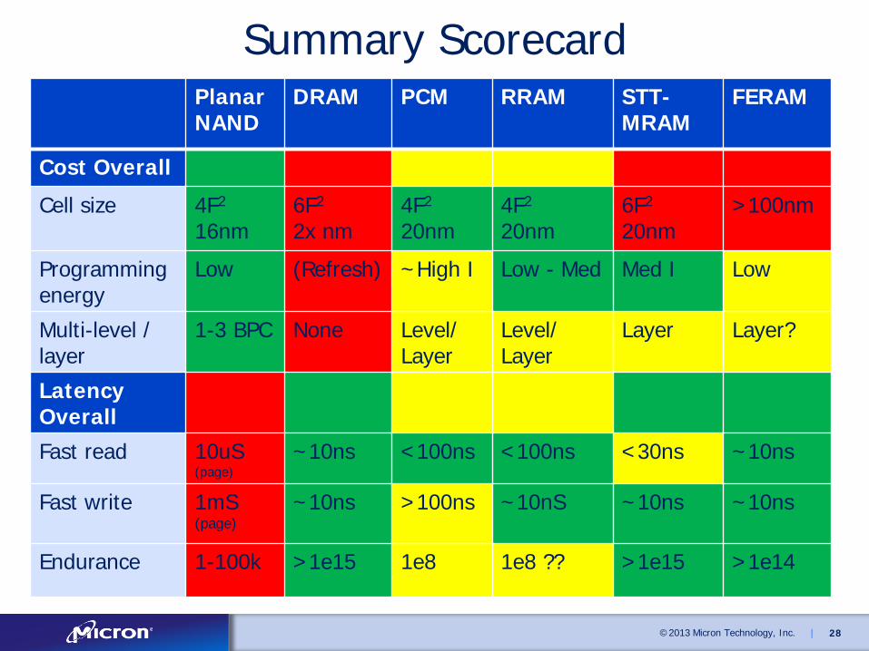
Summary Scorecard Planar NAND
DRAM PCM RRAM STT-MRAM
FERAM
Cost Overall
Cell size 4F2 16nm
6F2 2x nm
4F2 20nm
4F2 20nm
6F2
20nm >100nm
Programming energy
Low (Refresh) ~High I Low - Med Med I Low
Multi-level / layer
1-3 BPC None Level/ Layer
Level/ Layer
Layer Layer?
Latency Overall Fast read 10uS
(page) ~10ns <100ns <100ns <30ns ~10ns
Fast write 1mS (page)
~10ns >100ns ~10nS ~10ns ~10ns
Endurance 1-100k >1e15 1e8 1e8 ?? >1e15 >1e14

29 ©2013 Micron Technology, Inc. |
Where can an emerging memory fit in?
Latency NAND DISK DRAM
Bit/$ NAND DISK DRAM SCM
(Storage class memory)
Latency NAND DISK DRAM
Bit/$ NAND DISK DRAM NVDRAM
(Non-Volatile DRAM)
Latency NAND DISK DRAM
Bit/$ NAND DISK DRAM
NAND REPLACEMENT (STORAGE)

30 ©2013 Micron Technology, Inc. |
Summary ▶ Many new NVM technologies are attempting to gain a foothold in the
computing devices
▶ While they have cost or performance advantages over NAND or DRAM, none beat the performance of DRAM or the cost of NAND
▶ The most direct fit would be a NAND/DRAM “blend” / SCM, but the system implementation for this type of memory is not yet established
▶ We need a few more advances in materials to make these a reality!
▶ Acknowledgments: Thanks to the Micron R&D team and the work of the authors presented here.
