non-oxidizing purification method for large volumes of long, undamaged single-walled carbon...
TRANSCRIPT

Non-oxidizing Purification Method for Large Volumes of Long, Undamaged Single-WalledCarbon Nanotubes
Pornnipa Vichchulada, Jihye Shim, and Marcus D. Lay*Department of Chemistry and Nanoscale Science and Engineering Center (NanoSEC), UniVersity of Georgia,Athens, Georgia 30602
ReceiVed: May 6, 2008; ReVised Manuscript ReceiVed: October 20, 2008
A mild route to the purification of single-walled carbon nanotube (SWNT) soot has been investigated. Theremoval of all forms of impurities commonly found in bulk SWNT material (metal catalyst nanoparticles,amorphous carbon, and bundles of SWNTs) has been obtained. This technique, which involves purificationbased on centrifugation at low centrifugal force, results in deposits that are composed of individual SWNTsthat do not have the defects that result from harsh oxidative treatments. While ultracentrifugation has beenused to separate and purify raw SWNT soot, this method removes all but the shortest nanotubes. Therefore,it is not practical for many electronic applications. The method presented in this manuscript removescarbonaceous and metallic impurities, while leaving long undamaged SWNTs in suspension. A liquid depositionmethod under development in this group was used to form electrically continuous two-dimensional networksof SWNTs. Atomic force microscopy (AFM) then is used to verify the efficacy of centrifugation cycles forpurification of SWNT suspensions. AFM images of the deposits indicate significant improvement of depositmorphology, with long individual SWNTs that are observed without the presence of impurities. SWNT networksformed from these purified deposits behaved as metallic conductors at high density and as semiconductivethin films at low density. This further indicates that bundles of SWNTs were removed, along with otherundesirable materials.
Introduction
One of the major focuses of recent nanoscience investiga-tions is single-walled carbon nanotubes (SWNTs).1-7 Yet, as-produced (AP) grade SWNTs are composed of a mixture ofSWNTs (with varying physical and electronic properties),8-10
metal catalyst nanoparticles (which are used for the SWNTgrowth process), and amorphous carbon (a by-product of SWNTgrowth). These metal nanoparticles and carbonaceous impuritiesreduce the precision of SWNT device structures. Therefore, theremoval of these impurities is a major part of obtaining afundamental understanding of the properties and potentialapplications of SWNTs.
Various purification methods for SWNT suspensions havebeen extensively investigated.11-14 These purification methodsoften involve oxidizing chemical treatments that damage anddissolve catalyst particles and amorphous carbon at a greaterrate than they damage the SWNTs. Such protocols have beeneffective in reducing impurities in SWNT solutions. Yet,oxidative treatments also oxidize the ends (to a great extent)and sidewalls (to a lesser, but significant, extent) of SWNTs.This damage results in decreased mobility and conductivity ofthe SWNTs.15-17 Therefore, nondestructive methods of separat-ing impurities from SWNT material are of great importance.
One nondestructive method for the purification of SWNT sootinvolves ultracentrifugation. This involves the use of highcentrifugal forces (typically in excess of 100 000 G) to removeimpurities. This method is quite effective because carbonaceousand metallic impurities usually have higher density than veryshort, unbundled SWNTs.18 A drawback to this technique isthat it also removes long unbundled SWNTs, because of their
higher mass. However, for most macroscopic electronic ap-plications, SWNTs in excess of 1 µm in length are desirable.Therefore, a method of reproducibly removing impurities andleaving long, undamaged SWNTs in solution is of significantinterest. This manuscript presents results from this group thatinvolve the use of centrifugation cycles, at low centrifugal force,alone, to purify AP SWNT soot of all forms of impurities.
The effectiveness of this purification method can be inves-tigated using this group’s method for forming two-dimensionalnetworks of SWNTs on clean flat silicon wafer surfaces. Briefly,highly aligned arrays of SWNTs are deposited from aqueoussuspension in a “molecular combing” technique.19 Patterneddevice structures were fabricated from these deposits usingstandard optical lithography techniques.20 An advantage of thisdeposition technique over high-temperature growth methods isthat it allows the formation of purified, highly aligned networksof SWNTs with the desired density. In addition, because SWNTnetworks are formed at room temperature, heat-sensitivesubstrates such as plastics and glass, can also be used.Furthermore, chemical modification steps can be inserted eitherbefore or after network deposition.
The great variability in electrical properties from one SWNTto another makes device structures that are based on singleSWNTs impractical.21-23 However, the effect of this variabilityon device performance is ameliorated by the use of SWNTnetworks. For an SWNT network, performance is largelyaffected by the density of SWNTs, rather than the properties ofany individual SWNT; high-density networks behave as metallicconductors, while low-density networks behave as semicon-ductive thin films.24,25 Therefore, to achieve reproducibility indevice performance, it is unnecessary to separate SWNTs basedon metallic or semiconductive behavior, or confront the varyingbandgaps of semiconductive nanotubes. While SWNT network
* Author to whom correspondence should be addressed. E-mail: [email protected].
J. Phys. Chem. C 2008, 112, 19186–1919219186
10.1021/jp803989d CCC: $40.75 2008 American Chemical SocietyPublished on Web 11/17/2008

device structures are significantly larger than those based on asingle SWNT, such networks have widespread application inareas such as displays, solar energy conversion cells, and otherareas where large-area transparent thin films are useful.
A major advantage of SWNT networks is that the electricalresponse of the device structures is determined by the networkdensity, rather than internanotube variability. An importantcaveat to this rule is that large bundles of SWNTs must beminimized. Large bundles act as metallic wires that degradethe semiconductive properties of the thin film, resulting in adeposit that behaves more as a metal than as a semiconductor.Therefore, the observation of semiconductive behavior indicatesthe effective removal of bundles of SWNTs and other impuritiesthat exhibit metallic conduction, as well as the fact that thedesired network density has been reached.
There is great interest in incorporating SWNTs into electronicdevice structures, because of their enhanced electrical pro-perties.15,26-35 Therefore, the ability to deposit desired densitiesand orientations of purified SWNTs on surfaces is critical forthe creation of a wide variety of functional device structures.An excellent method for determining the purity of these depositsis atomic force microscopy (AFM), because it routinely yieldssub-angstrom-level resolution in the z-direction. This allowsdistinction between individual SWNTs (tubes with a diameterof ∼1.4 nm) and various types of impurities (which are usuallyglobular).
Device structures formed from these purified suspensionsdemonstrated the strong dependence of device performance onthe network density that is expected from two-dimensional (2-D) SWNT networks; because two-thirds of the SWNTs aresemiconductors and one-third are metallic conductors,22,23 highdensities of SWNTs behaved as metallic conductors, whereaslow densities behaved as semiconductors. This behavior hasbeen explained by percolation theory.25
Experimental Section
SWNT Solution Preparation. For all the work herein, 25mg of unmodified SWNT soot (AP-grade, CarboLex, Inc.) wasdispersed in 25 mL of an aqueous solution of 1% (w/v) sodiumdodecyl sulfate (SDS, J.T. Baker) by probe sonication (Model500, Fisher). Dispersion involved probe sonication for 30 minat 12 W. Purification involved multiple centrifugation cycles at18 000 G for 45 min/cycle (Beckman, GS-15R). Each centrifu-gation was followed by carefully decanting the supernatant andcentrifuging again. The optimum conditions for obtaining long,unbundled SWNTs while reducing the concentration of impuri-ties to levels that would not have to reduce the observedelectrical behavior was determined to be five centrifuge/decantation cycles, as described previously.
Formation of SWNT Deposits through Laminar FlowDeposition. The ability of this method to purify SWNTsuspensions was verified using this group’s liquid laminar flowdeposition (LFD) method for the formation of two-dimensionalelectrical networks of SWNTs.36,37 This deposition techniqueis unlike drop-cast techniques, where bundles of SWNTs formduring the drying process, as the SWNT concentration exceedsits solubility as the solvent evaporates. The possibility of bundleformation during deposition is removed because they aredeposited in a manner that is similar to the molecular combingof DNA;38-44 unidirectional airflow is applied to the air/liquidinterface in a manner that imparts order to the SWNTs inaqueous suspension. This method allows SWNT networks tobe formed on a wide range of substrates (i.e., Si/SiOx, glass,
polymers, etc.). Furthermore, this method is fully compatiblewith existing optical lithography methods.
The Si-wafer surface was cleaned and modified before thedeposition of the SWNT solution. The Si-wafer was cut intofragments of 5 cm × 5 cm. The fragments were then cleanedwith a snow-jet (compressed CO2). A fresh 10 mM solution of3-amino-propyl-triethoxysilane in 99.5% ethanol was used toform a silane on the surface. The Si-wafer fragments weresoaked in the silane solution for 45 min, followed by rinsingwith a copious amount of fresh ethanol and then n-H2O. Thequality of the Si-wafer substrates was verified before SWNTdeposition by AFM imaging. After the silicon wafer substrateswere determined to be clean and flat on a sub-angstrom scale,they were used for SWNT deposition.
One deposition cycle is defined as wetting the surface with100 µL of SWNT suspension, followed by the use of high-purity N2 at 60 psi, to effect drying of the aqueous layer vialaminar flow. The N2 flow was directed at the surface througha hand-held air gun (Silvent) at an angle of 30°. The depositwas then washed with copious amounts of nanopure water toremove SDS residue. The density of SWNTs, as observed byexamination of AFM images, was determined to increase at arate of 0.33 SWNTs/µm2. Therefore, combinations of solutionconcentration and number of deposition cycles will afford strictcontrol over the density of SWNTs in a network.
Determination of the Extent of Purification of SWNTSuspensions. After forming a deposit, the extent of purificationwas determined using topographic AFM images (MolecularImaging, PicoPlus) to compare deposits formed from centrifugedsolutions with deposits formed from untreated standard solutions.Image analysis software (SPIP, Imagemet) was used to createa histogram of the frequency of observance versus height, todetermine the extent of purification, because the variousimpurities present were observed to be larger in height thanthe average SWNT. For the creation of these histograms, thelowest point on the surface was denoted as 0 nm and each pixelin the image above that value in height was placed in acorresponding bin. These histograms were formed for depositscreated from solutions at various stages of purification. Thesehistograms show what proportion of pixels in an AFM imagefall into each of several height categories. These heightcategories are defined as distance, in the z-direction, from thesubstrate. For low-density arrays of SWNTs that have beendeposited using LFD, this allows quantitation of the effect ofmultiple centrifugation cycles at low centrifugal force on theremoval of various forms of impurities.
The effectiveness of this purification protocol was alsoverified with ultraviolet and visible-light (UV-vis) spectroscopy(Varian, Carey 300) and Raman spectroscopy (Renishaw, inVia).UV-vis spectroscopy was performed on SWNT suspensionsin a liquid cell with a path length of 1 cm. However, for Ramanspectroscopy, the deposition method under development in thisgroup was used to form low-density arrays of SWNTs on aSi-wafer fragment. Raman spectra then were collected using acharge-coupled device (CCD) detector. Scattering was excitedusing a diode laser at a wavelength of 785 nm, and the powerthat was measured at the sample was 10 mW.
The effect of this purification method on electronic devicestructures was also determined. Separate Si-wafer fragments,containing an SWNT network deposited from an untreated andpurified suspension, were subjected to an optical lithographicpatterning step to create thin-film semiconductor transistors witha source-drain channel of 8 µm. Optical lithography (Suss, MA6)then was used to form source and drain electrodes on an SWNT-
Non-oxidizing Purification Method for SWNTs J. Phys. Chem. C, Vol. 112, No. 49, 2008 19187

network coated Si-wafer fragment. A conventional three-electrode transistor configuration then was used to test eachdevice. The electrical function of these networks was tested witha semiconductor characterization system (Keithley, 4200 SCS)and an analytical probe station (Signatone, S-1160).
Results and Discussion
AFM Analysis of SWNT Deposits Formed from LaminarFlow Deposition. Carbolex AP-grade arc discharge soot witha purity of 50-70 wt % SWNTs was used for all experiments.The remainder of the unpurified sample is typically residualcatalyst (Ni-Y) and amorphous carbon produced during thegrowth process. AFM analysis of indicated that the individualSWNTs had a mean diameter of 1.4 nm. This is consistent withpreviously reported electron microscopy studies of these typesof nanotubes.45-47 Bulk SWNT material consists of numerousbundles of ∼100 tubes. The nanotubes in these bundles adheretogether through van der Waals interactions along their side-walls. Therefore, deposition of individual SWNTs on a flatsurface requires imparting enough energy to the solution to breakapart these bundles without damaging the SWNTs.
Deposits formed from untreated solutions often result information of thin films that are unsuitable for device formation.Figure 1 shows the result of one deposition cycle on a Si-wafersubstrate. Although SWNTs are evident, the impurities depositedfrom the AP-SWNT solution degrade the overall quality of thisdeposit. Information about the quality of a deposit can beobtained from analysis of how far the average height measure-ment (Z-direction) differs from the expected height distributionfor a surface composed of a pure, low-density network ofSWNTs (1.4 nm for Carbolex AP grade arc-discharge SWNTs).A histogram of the height of all the pixels in Figure 1 indicatesthat the average Z-direction height observed is 2.5 nm, with asignificant contribution of greater heights. This is due to thepresence of globular impurities of greater height than theSWNTs.
The presence of various impurities in the deposition suspen-sion becomes more problematic as the number of depositioncycles increases. Five deposition cycles from a suspension ofAP-SWNTs shows that much of the surface is covered byimpurities (Figure 2). In addition, the histogram for the pixelsin the Z-direction shows an average height of 30 nm. TheSWNTs, at an average height of 1.4 nm, are dwarfed by thevarious impurities. Therefore, it is evident that purificationmethods are critical to the formation of low-density networksof SWNTs and, consequently, for the application of thesenetworks to functional device structures.
After two centrifugation cycles, the same number of deposi-tion cycles used in Figure 2 was used to form a deposit (Figure3). AFM images indicated the formation of an electricallycontinuous carbon nanotube network with a significantly lowerdensity of impurities on the surface than that formed from theAP-SWNT solution. The histogram for this deposit indicatesthat the average height was 2.2 nm. This is roughly an order-of-magnitude-lower height than that observed for the untreatedsolution, as a large portion of the impurities settled out of thesolution, because of their greater density and/or lower solubilityin SDS.
Five centrifugation cycles resulted in a remarkable decreasein the number of catalyst particles observed on the surface afterdepositing SWNTs from these purified solutions (see Figure 4a).SWNTs with a length of 1-3 µm were observed, indicatingthat, although the centrifugation cycles were very efficient atremoving bundles of carbon nanotubes, carbonaceous impurities
and catalyst nanoparticles, high-aspect-ratio carbon nanotubesremain on the surface. Furthermore, analysis of the AFM datashows that the average height of all of the pixels on the surfaceis 1.4 nm, which is the average height of the SWNTs in thissample (see Figure 4b). This indicates that multiple centrifuga-tion cycles at low G are an efficient means of removing largebundles of SWNTs, as well as carbonaceous material andnanoparticles while leaving long undamaged SWNTs in suspen-sion. The result is a greatly improved deposit formed via LFD.
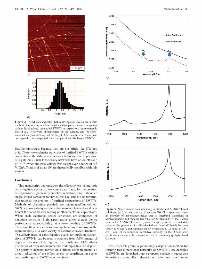
Spectroscopy of SWNT Suspensions and Deposits. Absor-bance measurements were obtained for AP and a purifiedsuspension of SWNTs. The UV-vis spectra for these suspen-sions (see Figure 5a) show the first interband transitions formetallic (M11, 400-650 nm) and semiconducting (S22, 550-900nm) SWNTs.48,49 The absorbance due to these transitions is notvisible in the untreated solutions. The increase in the sharpnessof these peaks between the AP- and purified-solutions can beattributed to the removal of impurities and the enrichment ofpurified, unbundled SWNTs.
Raman spectroscopy was used to determine the effectivenessof this purification method at removal of amorphous carbon.The Raman spectrum for AP-SWNT soot is typical for sp2
hybridized C atoms (see Figure 5b). It shows the presence of a
Figure 1. AFM image and histogram of deposit formed from onedeposition cycle from an unpurified SWNT suspension with a concen-tration of 1 mg/mL SWNT soot. (a) AFM image and (b) a heighthistogram showing that the SWNTs, at a height of ∼1.4 nm, are dwarfedby various impurities.
19188 J. Phys. Chem. C, Vol. 112, No. 49, 2008 Vichchulada et al.

disorder-induced band (D-band) in the range of 1300-1370cm-1. The D-band indicates the presence of disordered sp2 bondcaused by various anomalies such as C-atom vacancies, impuri-ties in the C lattice, or any other form of contamination.50,51
The high-frequency band (G-band) typically observed in thepristine, symmetrical graphene lattice is present at 1591cm-1.52,53 Figure 5c shows Raman spectra observed afterpurification. The mild route to purification described hereinresulted in an 11-fold increase of the G-band/D-band ratio. Therelative reduction of the D-band indicates purification of theraw SWNT soot. The decrease in the D-band also indicates thatthe SWNTs that remain have a lower level of defects. This isnot the case for acid-purified SWNTs, as oxidizing purificationprotocols create numerous defects sites along the ends andsidewalls of SWNTs.54
Comparison of Macroscopic Electrical Response of Un-treated and Treated SWNT Suspensions. SWNT networksformed with this group’s LFD method are completely compat-ible with current optical lithography techniques; a simpletransistor configuration was formed from lithographically pat-terned electrodes (see Figure 6) to compare the electricalresponse of thin-films formed from untreated versus purified
suspensions. Photoresist was spin-cast on the Si-wafer fragmentafter SWNT deposition. The use of metal deposition and “lift-off” on lithographically patterned photoresist then was used toform source and drain electrodes. This process was performedon untreated and purified SWNT suspensions.
In a device configuration designed to test semiconductor thinfilms, deposits that formed from untreated SWNT suspensionsexhibited metallic behavior, with a gate voltage of (3 V havinglittle effect on the source drain current (see Figure 7). This isdue to the presence of large bundles of SWNTs, metalnanoparticles, and amorphous carbon. All of these impuritiesconduct electricity but do not act as semiconductors.
Alternatively, low-density networks of purified and unbundledSWNTs behave as 2-D semiconductive thin films (Figure 7b).Because SWNTs are a mixture of one-third metallic materialand two-thirds semiconductive wires, bundles of SWNTs havea tendency to exhibit metallic conduction, due in large part tothe presence of metallic nanotubes in the bundles. Consequently,an optimized SWNT network-based device has tunable electricalconductivity that can be controlled by a gate voltage.
Therefore, low-density networks of SWNTs are useful as apossible alternative to transparent semiconductive materials suchas indium tin oxide (ITO) or amorphous Si (a-Si). In addition,such low-density SWNT thin films are also compatible with
Figure 2. (a) Repeated deposition cycles, using an AP-SWNT solution,results in a poor-quality deposit, as observed by AFM. (b) The surfaceis largely covered by impurities remaining from the growth process ofthe SWNTs, which caused an average height in the z-direction of 30nm.
Figure 3. (a) After two centrifugation cycles, the same depositionconditions that led to the deposit in Figure 2 lead to an electricallycontinuous network of SWNTs and a greatly reduced coverage ofimpurities. (b) Height histogram showing that the average heightobserved is 2.2 nm.
Non-oxidizing Purification Method for SWNTs J. Phys. Chem. C, Vol. 112, No. 49, 2008 19189
flexible substrates, because they are not brittle like ITO anda-Si. These lower-density networks of purified SWNTs exhibitconventional thin-film semiconductor behavior upon applicationof a gate bias. Such low-density networks have an on/off ratioof >102, when the gate voltage was swept over a range of (3V. On/off ratios of up to 106 are theoretically possible with thissystem.
Conclusions
This manuscript demonstrates the effectiveness of multiplecentrifugation cycles, at low centrifugal force, for the creationof suspensions significantly enriched in pristine, long, unbundledsingle-walled carbon nanotubes (SWNTs). This is a nondestruc-tive route to the creation of purified suspensions of SWNTs.Methods of obtaining purified, yet undamaged/unmodified,SWNTs allow subsequent steps that involve chemical modifica-tion of the nanotubes for sensing or other electronic applications.When such electronic device structures are composed ofnanotube networks, high aspect ratios allow greater deviceperformance reproducibility, at a lower loading of SWNTs.Therefore, these suspensions have applications in improving thereproducibility of a wide variety of electronic device structures.The effectiveness of centrifugation cycles for purifying suspen-sions of SWNTs can be readily obtained from AFM images ofdeposits. Because of its high vertical resolution, AFM allowsdistinction of even sub-nanometer-sized impurities in a deposit.The purity of deposits formed on a silicon wafer fragment is adirect indication of the effectiveness of centrifugation cyclesand purifying raw SWNT soot solutions.
This research group is pioneering a deposition method forforming two-dimensional networks of SWNTs. Low densitiesof SWNTs are deposited onto a prepared surface in successivedeposition cycles. Each deposition cycle puts down more
Figure 4. AFM data indicates that centrifugation cycles are a mildmethod of removing residual metal catalyst particles and amorphouscarbon, leaving long, unbundled SWNTs in suspension: (a) topographicplot of a 2-D network of nanowires on the surface, and (b) cross-sectional analysis showing that the height of the nanotubes in the depositcorrespond to that expected for a sample of arc discharge SWNTs.
Figure 5. Spectroscopic data indicating purification of AP-SWNT sootsolutions: (a) UV-vis spectra of aqueous SWNT suspensions showan increase of absorbance peaks due to interband transitions insemiconductive and metallic SWNT after purification; (b) the Ramanspectra for AP-SWNT soot is typical for sp2 hybridized C material,showing the presence of a disorder-induced band (D-band) between1300-1370 cm-1, and symmetrical sp2 hybridized C (G-band) at 1591cm-1; and (c) the reduction in relative intensity for the D-band afterpurification indicated the removal of defect containing sp2 hybridizedC atoms.
19190 J. Phys. Chem. C, Vol. 112, No. 49, 2008 Vichchulada et al.

SWNTs until the desired network density is attained. Three-electrode transistor response showed that high-density networks
behaved as low-resistance transparent thin films, whereas low-density networks show traditional semiconductor behavior.
Acknowledgment. The authors thank the University ofGeorgia Research Foundation for financial support.
References and Notes
(1) Borondics, F.; Kamaras, K.; Nikolou, M.; Tanner, D. B.; Chen,Z. H.; Rinzler, A. G. Phys. ReV. B 2006, 74.
(2) Yu, B.; Meyyappan, M. Solid-State Electron. 2006, 50, 536.(3) Wang, M. S.; Peng, L. M.; Wang, J. Y.; Chen, Q. AdV. Funct.
Mater. 2006, 16, 1462.(4) Perfetto, E.; Gonzalez, J. J. Phys.: Condens. Matter 2006, 18,
S2105.(5) Rowell, M. W.; Topinka, M. A.; McGehee, M. D.; Prall, H. J.;
Dennler, G.; Sariciftci, N. S.; Hu, L. B.; Gruner, G. Appl. Phys. Lett. 2006,88.
(6) Ozel, T.; Gaur, A.; Rogers, J. A.; Shim, M. Nano Lett. 2005, 5,905.
(7) Bellucci, S.; Cini, M.; Onorato, P.; Perfetto, E. J. Phys.: Condens.Matter 2006, 18, S2115.
(8) Venema, L. C.; Janssen, J. W.; Buitelaar, M. R.; Wildoer, J. W. G.;Lemay, S. G.; Kouwenhoven, L. P.; Dekker, C. Phys. ReV. B 2000, 62,5238.
(9) Venema, L. C.; Meunier, V.; Lambin, P.; Dekker, C. Phys. ReV. B2000, 61, 2991.
(10) Wildoer, J. W. G.; Venema, L. C.; Rinzler, A. G.; Smalley, R. E.;Dekker, C. Nature 1998, 391, 59.
(11) Huang, H. J.; Maruyama, R.; Noda, K.; Kajiura, H.; Kadono, K. J.Phys. Chem. B 2006, 110, 7316.
(12) Yu, G. J.; Gong, J. L.; Wang, S.; Zhu, D. Z.; He, S. X.; Zhu, Z. Y.Carbon 2006, 44, 1218.
(13) Chen, Y.; Tang, Y. W.; Kong, L. Y.; Liu, C. P.; Xing, W.; Lu,T. H. Acta Phys. Chim. Sin. 2006, 22, 119.
(14) Tohji, K.; Goto, T.; Takahashi, H.; Shinoda, Y.; Shimizu, N.;Jeyadevan, B.; Matsuoka, I.; Saito, Y.; Kasuya, A.; Ohsuna, T.; Hiraga,H.; Nishina, Y. Nature 1996, 383, 679.
(15) Tunney, M. A.; Cooper, N. R. Phys. ReV. B 2006, 74.(16) Robinson, J. A.; Snow, E. S.; Badescu, S. C.; Reinecke, T. L.;
Perkins, F. K. Nano Lett. 2006, 6, 1747.(17) Wang, M.; Zhang, X.; Lu, M. W.; Liu, Y. Appl. Phys. Lett. 2006,
88.(18) O’Connell, M. J.; Bachilo, S. M.; Huffman, C. B.; Moore, V. C.;
Strano, M. S.; Haroz, E. H.; Rialon, K. L.; Boul, P. J.; Noon, W. H.; Kittrell,C.; Ma, J. P.; Hauge, R. H.; Weisman, R. B.; Smalley, R. E. Science 2002,297, 593.
(19) Vichchulada, P.; Zhang, Q.; Lay, M. D. Analyst 2007, 132, 709.(20) Lay, M. D.; Novak, J. P.; Snow, E. S. Nano Lett. 2004, 4, 603.(21) Liebau, M.; Graham, A. P.; Duesberg, G. S.; Unger, E.; Seidel,
R.; Kreupl, F. Fullerenes, Nanotubes, Carbon Nanostruct. 2005, 13, 255.(22) Dresselhaus, M. S.; Dai, H. MRS Bull. 2004, 29, 237.(23) Dai, H. J. Surf. Sci. 2002, 500, 218.(24) Edgeworth, J. P.; Wilson, N. R.; Macpherson, J. V. Small 2007, 3,
860.(25) Hu, L.; Hecht, D. S.; Gruner, G. Nano Lett. 2004, 4, 2513.(26) Obradovic, B.; Kotlyar, R.; Heinz, F.; Matagne, P.; Rakshit, T.;
Giles, M. D.; Stettler, M. A.; Nikonov, D. E. Appl. Phys. Lett. 2006, 88,142102.
(27) Ouyang, Y.; Yoon, Y.; Fodor, J. K.; Guo, J. Appl. Phys. Lett. 2006,89, 203107.
(28) d’Honincthun, H. C.; Galdin-Retailleau, S.; See, J.; Dollfus, P. Appl.Phys. Lett. 2005, 87, 172112.
(29) Guo, J.; Kan, E. C.; Ganguly, U.; Zhang, Y. G. J. Appl. Phys. 2006,99, 084301.
(30) Wang, K.; Fishman, H. A.; Dai, H. J.; Harris, J. S. Nano Lett. 2006,6, 2043.
(31) Artyukhin, A. B.; Stadermann, M.; Friddle, R. W.; Stroeve, P.;Bakajin, O.; Noy, A. Nano Lett. 2006, 6, 2080.
(32) Chen, Y. F.; Fuhrer, M. S. Nano Lett. 2006, 6, 2158.(33) Graber, M. R.; Coish, W. A.; Hoffmann, C.; Weiss, M.; Furer, J.;
Oberholzer, S.; Loss, D.; Schonenberger, C. Phys. ReV. B 2006, 74.(34) Durkop, T.; Getty, S. A.; Cobas, E.; Fuhrer, M. S. Nano Lett. 2004,
4, 35.(35) Javey, A.; Guo, J.; Wang, Q.; Lundstrom, M.; Dai, H. J. Nature
2003, 424, 654.(36) Vichchulada, P.; Lipscomb, L. D.; Zhang, Q.; Lay, M. D. J.
Nanosci. Nanotechnol. 2008, In press.(37) Vichchulada, P.; Zhang, Q.; Lay, M. D. Analyst 2007, 132, 719.(38) Woolley, A. T.; Kelly, R. T. Nano Lett. 2001, 1, 345.(39) Yokota, H.; Sunwoo, J.; Sarikaya, M.; van den Engh, G.; Aebersold,
R. Anal. Chem. 1999, 71, 4418.
Figure 6. An SWNT network transistor: (a) Diagram of an SWNTnetwork device fabricated on a Si/SiOx wafer fragment. The sourceand drain electrodes are vapor deposited onto the network using standardoptical lithography methods, and the doped silicon will be used as aback-gate; (b) Scanning electron microscopy (SEM) (top) and atomicforce microscopy (AFM) (bottom) images of a SWNT network device.
Figure 7. Electrical response of two SWNT networks while scanningthe gate voltage: (a) high-density and/or low-quality networks, as seenin Figure 2a, behave as metallic conductors, (b) while purified, low-density networks, as seen in Figure 4a, have tunable conductance.
Non-oxidizing Purification Method for SWNTs J. Phys. Chem. C, Vol. 112, No. 49, 2008 19191

(40) Allemand, J. F.; Bensimon, D.; Jullien, L.; Bensimon, A.; Croquette,V. Biophys. J. 1997, 2064.
(41) Ouyang, Z. Q.; Hu, J.; Chen, S. F.; Sun, J. L.; Li, M. Q. J. Vac.Sci. Technol. B 1997, 15, 1385.
(42) Hu, J.; Wang, M.; Weier, H. U. G.; Frantz, P.; Kolbe, W.; Ogletree,D. F.; Salmeron, M. Langmuir 1996, 12, 1697.
(43) Bensimon, D.; Simon, A. J.; Croquette, V.; Bensimon, A. Phys.ReV. Lett. 1995, 74, 4754.
(44) Bensimon, A.; Simon, A.; Chiffaudel, A.; Croquette, V.; Heslot,F.; Bensimon, D. Science 1994, 265, 2096.
(45) Cui, J. B.; Daghlian, C. P.; Gibson, U. J. J. Appl. Phys. 2005, 98.(46) Valentini, L.; Armentano, I.; Biagiotti, J.; Frulloni, E.; Kenny, J. M.;
Santucci, S. Diamond Relat. Mater. 2003, 12, 1601.(47) Zhao, J. L.; Jiang, C. Y.; Fan, Y. W.; Burghard, M.; Basche, T.;
Mews, A. Nano Lett. 2002, 2, 823.(48) Lian, Y. F.; Maeda, Y.; Wakahara, T.; Akasaka, T.; Kazaoui, S.;
Minami, N.; Choi, N.; Tokumoto, H. J. Phys. Chem. B 2003, 107, 12082.
(49) Maeda, Y.; Kimura, S.; Kanda, M.; Hirashima, Y.; Hasegawa, T.;Wakahara, T.; Lian, Y. F.; Nakahodo, T.; Tsuchiya, T.; Akasaka, T.; Lu, J.;Zhang, X. W.; Gao, Z. X.; Yu, Y. P.; Nagase, S.; Kazaoui, S.; Minami, N.;Shimizu, T.; Tokumoto, H.; Saito, R. J. Am. Chem. Soc. 2005, 127, 10287.
(50) Dresselhaus, M. S.; Dresselhaus, G.; Jorio, A.; Souza, A. G.; Saito,R. Carbon 2002, 40, 2043.
(51) Shin, H. J.; Kim, S. M.; Yoon, S. M.; Benayad, A.; Kim, K. K.;Kim, S. J.; Park, H. K.; Choi, J. Y.; Lee, Y. H. J. Am. Chem. Soc. 2008,130, 2062.
(52) Brown, S. D. M.; Corio, P.; Marucci, A.; Pimenta, M. A.;Dresselhaus, M. S.; Dresselhaus, G. Phys. ReV. B 2000, 61, 7734.
(53) Corio, P.; Brown, S. D. M.; Marucci, A.; Pimenta, M. A.; Kneipp,K.; Dresselhaus, G.; Dresselhaus, M. S. Phys. ReV. B 2000, 61, 13202.
(54) Furtado, C. A.; Kim, U. J.; Gutierrez, H. R.; Pan, L.; Dickey, E. C.;Eklund, P. C. J. Am. Chem. Soc. 2004, 126, 6095.
JP803989D
19192 J. Phys. Chem. C, Vol. 112, No. 49, 2008 Vichchulada et al.