nomenclature design of the series resonant …ecee.colorado.edu/~rwe/references/aes86.pdf · design...
TRANSCRIPT

NOMENCLATURE
Design of the SeriesResonant Converter forMinimum ComponentStress
A.F. WITULSKI
R.W. ERICKSON, Member, I.E.E.E.University of Colorado
For a given output voltage and power, the peak resonant
capacitor voltage and peak inductor and switch currents of the
series resonant converter depend strongly on the choice of
transformer turns ratio and of tank inductance and capacitance. In
this paper the particular component values which result in the
smallest component stresses are determined, and a simple design
strategy is developed. The procedure is illustrated for an off-line
200 W, 5 V application, and it is shown that an incorrect choice of
component values can result in significantly higher component
stresses than are necessary.
Manuscript received October 3, 1985.
This work supported in part by IBM Corp., Boulder, Colo., and by theGeneral Electric Foundation.
Authors' address: Department of Electrical and Computer Engineering,University of Colorado, Campus Box 425, Boulder, CO 80309.
0018-9251/86/0700-0356 $1.00 X) 1986 IEEE
Cfo
I,LPJJLPJokLM
nPORloadRoSiS2VvcpVgViny(WO
Resonant (tank) capacitance.Resonant frequency of the tank circuit.Switching frequency.Output current of the converter.Peak value of inductor current.Normalized output current.Normalized peak inductor current.Intercept used in linear approximations (19)-(22).Mode index.Resonant (tank) inductance.Normalized output voltage.Normalized peak voltage on the tank capacitor.Transformer turns ratio.Output power.Load resistance.Characteristic impedance of the tank circuit.Stress function for tank components.Stress function for switching transistors.Output voltage of the converter.Peak voltage on the tank capacitor.Voltage on the dc blocking capacitors, Cl and C2.DC input voltage.Normalized switching frequency.Angular resonant frequency (in radians persecond).
1. INTRODUCTION
In the design of the series resonant converter, Fig. 1,it is necessary to select values of resonant inductance,capacitance, and transformer turns ratio to obtain a givenoutput voltage and power. Experience has shown thatpeak component stresses can vary by an order ofmagnitude or more depending on the choice of thesecomponent values. It is not clear at first which values ofcharacteristic tank impedance RO = /LW7 andtransformer turns ratio n result in the lowest overallstresses. Therefore it is of interest to seek a systematicmethod of choosing the characteristic impedance andturns ratio to achieve the goal of an efficient design.
A solution to this design problem is based on theexact transcendental equations [1, 2] which relate thepeak capacitor voltage and tank current to the outputvoltage and current, the transformer turns ratio, and thecharacteristic tank impedance. Approximation of theseexact expressions provides simple explicit equations forpeak voltage and current in terms of the other quantities.Next, as a measure of component size, two stressfunctions are defined in terms of the peak voltage andcurrent. one for stress on the resonant capacitor andinductor, and one for stress on the switching transistors.The minima of these stress functions are then found;these minima represent the value of tank impedance andtransformer turns ratio that result in the smallestcomponents and the most cost-effective design. However,in some cases the approximate expressions are not
IEEE TRANSACTIONS ON AEROSPACE AND ELECTRONIC SYSTEMS VOL. AES-22, NO. 4 JULY 1986356

I (t)+VC (t)
Q? 2 C2 Vg
CutT -
Fig. 1. Schematic of half-bridge series resonant converter.
accurate enough, and hence iterative computer routinesare employed to refine the answers given by theapproximate method. Finally, to illustrate the results ofthe analysis, a design example is given in which the sameset of specifications is satisfied by a number of differentdesigns, and it is shown that stresses are far lower at therecommended operating points.
11. THE NORMALIZED OUTPUT PLANE
Clearly the specification of output voltage and currentis equivalent to the choice of an operating point (V, I) inthe unnormalized output plane. However, it is possible toobtain the same V and I in many different ways byvariation of characteristic impedance, turns ratio, andswitching frequency. In order to generalize the problemof finding the best component values for a given V and I,we can normalize the output voltage and load impedanceas follows:
MV
M=- ~~~~~~~~~~~~~~(1)nlVg
R - Rload (2)
The output voltage is normalized with respect to the turnsratio, and the load impedance normalized with respect tothe tank impedance. Division of normalized outputvoltage by the normalized load yields the normalizedoutput current:
_ nROIg
(3)
We can now speak of finding the normalizedoperating point (M, J) that yields the lowest peak stressesfor a given amount of output power. When M and J aredenormalized for a specific output voltage and current,they yield the values of characteristic impedance andtransformer turns ratio which minimize the peak stressesfor the given application. Furthermore, since the outputcharacteristics of the series resonant converter are knownfor constant switching frequency [1], we may relate theoperating point (M, J) to its corresponding switchingfrequency through (4)
J = 2 ( -)k` + k + (-1) + 1)
+V -+1( +2 ) y (4)
where y = Trfo/f, is the normalized switching frequencyand k = 0, 1, 2, . . ., is the mode index. This equationis valid for any continuous conduction mode k as long asthe switching frequency is in the range
fo cf fo(1 + k) -S- k . (5)
For constant values of switching frequency, (4) describesa family of ellipses on the output plane. We are now in aposition to relate the generalized operating point (M, J) tothe peak capacitor voltage Vcp and the peak inductorcurrent ILP-
III. EXACT AND APPROXIMATE EXPRESSIONS FORPEAK VOLTAGE AND CURRENT
In this section the exact expressions relating peakresonant voltage and current to output voltage and currentare reviewed, and linear explicit equations for the peakstresses are developed by approximation of the exactequations.
As shown in [1], the combination of (4) with circuitequations containing peak voltage and current enables oneto obtain a set of equations relating the normalized outputcurrent to either Vcp and M, or ILP and M. To beconsistent with the normalized output variables, wenormalize peak capacitor voltage and inductor current inthe same manner as the output quantities.
m vcPM Vc
g
JLP R° LPg
The derivation of the equations is given in [1], and theresults are summarized here for convenience.
Above resonance (k = 0):
(8)MCP
tan- 1 /(MCP+ 1)2 11 - M2
J LP- 1 + M
tan -1(JLP + M)2 - 11 - M2
1 -M2for M < JLm JLP
(6)
(7)
(9)
WITULSKI & ERICKSON: SERIES RESONANT CONVERTER DESIGN 357
-l1 + 1,- JLP/(l -M2)tan- 1(JLP/(l - M2))
for1 -M2M JLP(10
Below resonance (k = 1):
J MCP (111/an(MCP- 1)2 -1r-tan l~/(M 1 m2 1
J = JLP + 1 - M (12)IT - tan V(JLP -M)2 - 1
sT-tan ff1 - m2
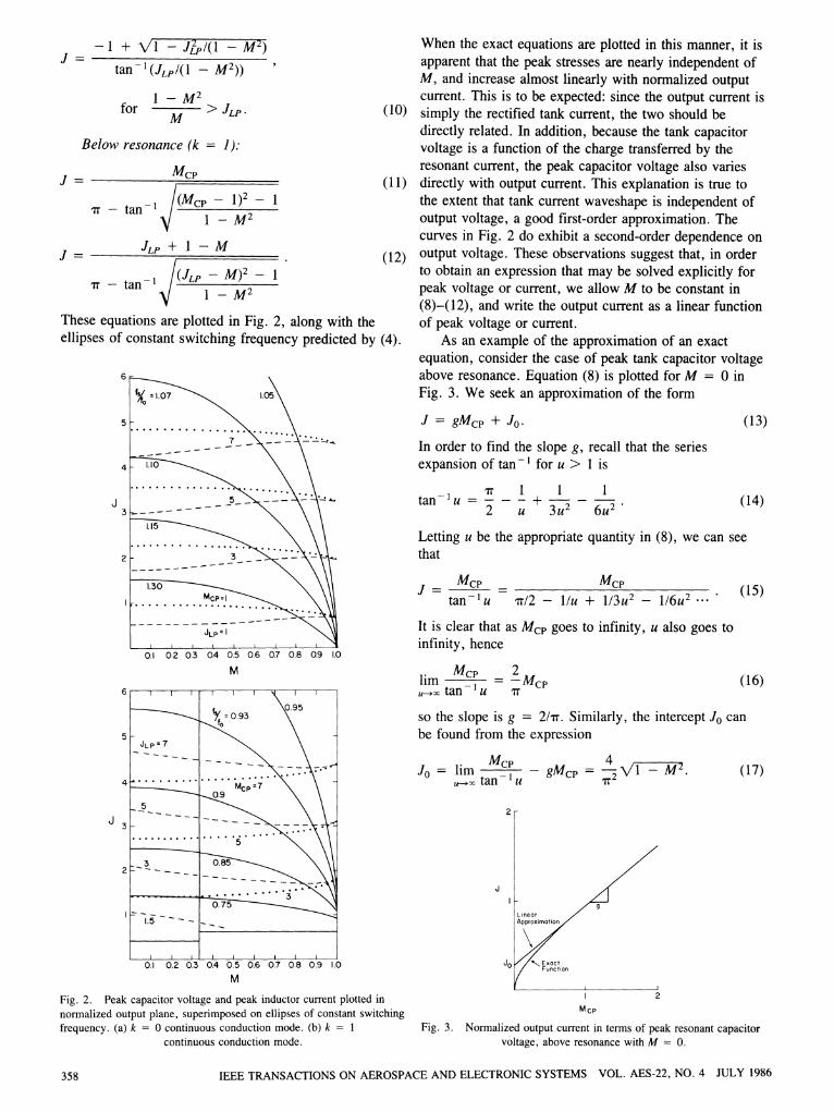
These equations are plotted in Fig. 2, along with theellipses of constant switching frequency predicted by (4).
6 F
J
When the exact equations are plotted in this manner, it isapparent that the peak stresses are nearly independent ofM, and increase almost linearly with normalized outputcurrent. This is to be expected: since the output current issimply the rectified tank current, the two should bedirectly related. In addition, because the tank capacitorvoltage is a function of the charge transferred by theresonant current, the peak capacitor voltage also variesdirectly with output current. This explanation is true tothe extent that tank current waveshape is independent ofoutput voltage, a good first-order approximation. Thecurves in Fig. 2 do exhibit a second-order dependence onoutput voltage. These observations suggest that, in orderto obtain an expression that may be solved explicitly forpeak voltage or current, we allow M to be constant in(8)-(12), and write the output current as a linear functionof peak voltage or current.
As an example of the approximation of an exactequation, consider the case of peak tank capacitor voltageabove resonance. Equation (8) is plotted for M = 0 inFig. 3. We seek an approximation of the form
J = gMcp + Jo0In order to find the slope g, recall that the seriesexpansion of tan- 1 for u > 1 is
- X 1 1 1tan lu = - - - + - - - '
2 U 3u2 62
(13)
(14)
Letting u be the appropriate quantity in (8), we can seethat
MCP Mcp (5tan- 1u - /2 - 1/u + 1/3u2 - 1/6u2 (. )
It is clear that as Mcp goes to infinity, u also goes toinfinity, hence
M
J
M
Fig. 2. Peak capacitor voltage and peak inductor current plotted innormalized output plane, superimposed on ellipses of constant switchingfrequency. (a) k = 0 continuous conduction mode. (b) k = 1
continuous conduction mode.
MP2lim C =-MCPU-- tan -u T
(16)
so the slope is g = 2/rr. Similarly, the intercept JO canbe found from the expression
JO = lim t I - 4 m .~-tan 1 ugmp
W(17)
2Mcp
Fig. 3. Normalized output current in terms of peak resonant capacitorvoltage, above resonance with M = 0.
IEEE TRANSACTIONS ON AEROSPACE AND ELECTRONIC SYSTEMS VOL. AES-22, NO. 4 JULY 1986358
Substitution of the slope and intercept into (13) yields an By recalling the definition ofM and J from Section II,explicit equation for Mcp: one can see that the output power P0 = VI is
IT 2m = -J - -VVM2
2 IT(18) Po= R
O(24)
When this process is repeated for the other peak stressesabove and below resonance, the following results areobtained.
Above resonance (k = 0):
IT 2MC= -- - (19)2 IT
JLP = -J - (M 1 + Tr2) (20)2 \ I T
Below resonance (k = 1):
I7T 2MCP=-J+-J-2 (21)2 IT
JLP=-J+n M- 1 +±2I (22)2 7r
These approximations agree well with our intuitiveexplanation of the converter behavior. In fact, whenM = 1 the intercept reduces to zero in each case. Theresulting expression for peak voltage or current is IT/2times the average output current. This corresponds to thepeak-to-average ratio of a rectified sine wave, andcorrectly models the converter behavior at resonance.Similar approximations have previously been made forthe parallel resonant converter [31. In summary, (19)-(22) are the explicit approximate equations needed tosolve for the operating points with minimum stress.
IV. TANK COMPONENT STRESS
In order to quantify the effect that the characteristictank impedance RO and transformer turns ratio n have onthe tank inductor and capacitor, a function is defined inthis section that relates Ro and n to the peak stresses onthese components. The minimum of this function yieldsthe desired operating point with lowest componentstresses and the best values of Ro and n.
One measure of the size of the resonant inductor andcapacitor is the magnitude of the peak energy stored ineach element during each switching cycle. Hence anelementary stress function could be the sum of the peakenergy in the two components:
S =-LI+2 CV1p.2 Lp 2 CC (23)
However, if we simply vary the peak voltage and current,then the output voltage and current will vary as well.Therefore it is necessary to normalize (23) with respect tothe output power. The stress function then becomes theratio of the peak energy stored in the inductor andcapacitor to the average energy transferred to the output.
Combination of (23) and (24) yields the stress function
1 1LI2p + 2CVC2P
S, = MJVg2RO (25)
Consider first the below-resonance case. Recalling thefact that peak stresses are nearly independent ofnormalized output voltage M, we choose M = 1 as thesimplest form of (21) and (22) and substitute the resultingexpressions into (25):
S L(Vg/RO)2((IT/2)J)2 + CVg2((IT/2)J)2S1 2MJV2/R (26)O
The definiton of the characteristic tank impedance Ro =
woL = 1/woC can be applied to eliminate Ro from (26):
4w1oM (27)
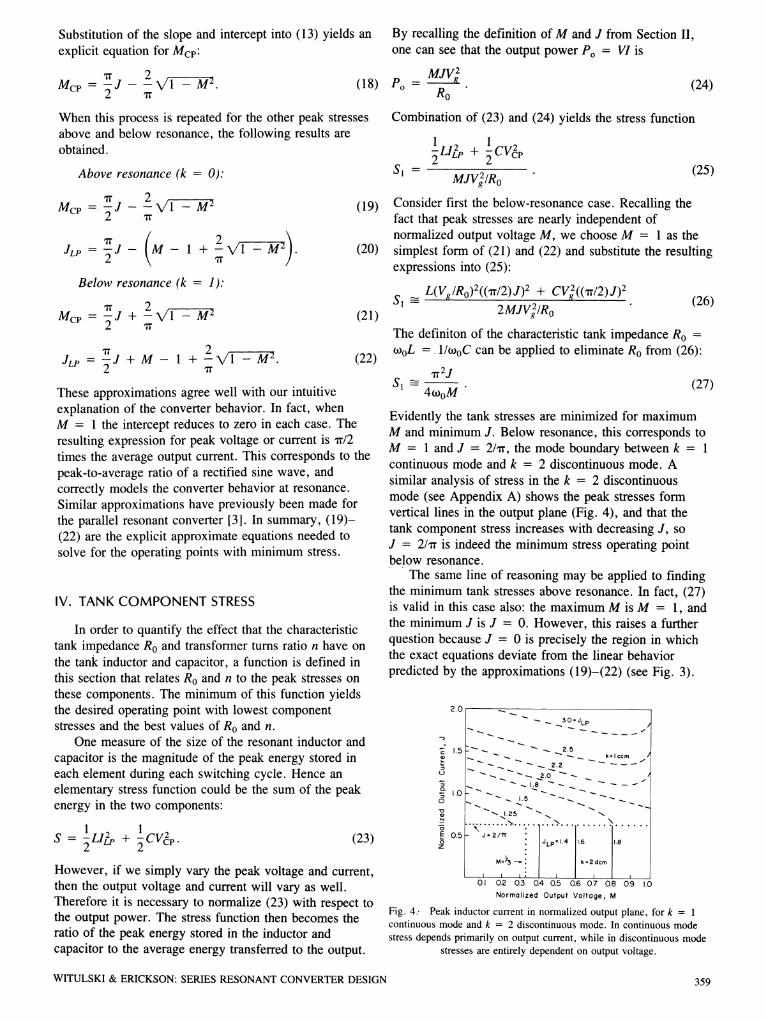
Evidently the tank stresses are minimized for maximumM and minimum J. Below resonance, this corresponds toM = 1 and J = 2/IT, the mode boundary between k = 1continuous mode and k = 2 discontinuous mode. Asimilar analysis of stress in the k = 2 discontinuousmode (see Appendix A) shows the peak stresses formvertical lines in the output plane (Fig. 4), and that thetank component stress increases with decreasing J, soJ = 2/PT is indeed the minimum stress operating pointbelow resonance.
The same line of reasoning may be applied to findingthe minimum tank stresses above resonance. In fact, (27)is valid in this case also: the maximum M is M = 1, andthe minimum J is J = 0. However, this raises a furtherquestion because J = 0 is precisely the region in whichthe exact equations deviate from the linear behaviorpredicted by the approximations (19)-(22) (see Fig. 3).
2.0_3.0 = Jp3 LP
15 *> . - \' cc
E.5 -2
1..10-
M23 2 dcm
V -~~~~~~~~~~
0.1 0.2 0.3 0.4 0.5 0.6 0.7 0.8 0.9 1.0
Normalized Output Voltage, M
Fig. 4. Peak inductor current in normalized output plane, for k = 1continuous mode and k = 2 discontinuous mode. In continuous modestress depends primarily on output current, while in discontinuous mode
stresses are entirely dependent on output voltage.
WITULSKI & ERICKSON: SERIES RESONANT CONVERTER DESIGN
(26)
359
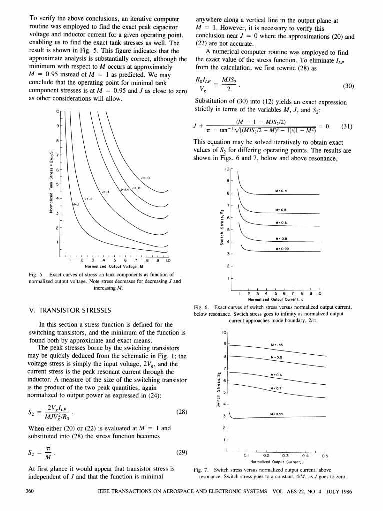
To verify the above conclusions, an iterative computerroutine was employed to find the exact peak capacitorvoltage and inductor current for a given operating point,enabling us to find the exact tank stresses as well. Theresult is shown in Fig. 5. This figure indicates that theapproximate analysis is substantially correct, although theminimum with respect to M occurs at approximatelyM = 0.95 instead of M = 1 as predicted. We mayconclude that the operating point for minimal tankcomponent stresses is at M = 0.95 and J as close to zeroas other considerations will allow.
10
9
8
3
cq
,,
nI-
a)Ez
7
6
5
4
3
2
anywhere along a vertical line in the output plane atM = 1. However, it is necessary to verify thisconclusion near J = 0 where the approximations (20) and(22) are not accurate.
A numerical computer routine was employed to findthe exact value of the stress function. To eliminate ILPfrom the calculation, we first rewrite (28) as
ROILp MJS2Vg 2 (30)
Substitution of (30) into (12) yields an exact expressionstrictly in terms of the variables M, J, and S2:
(M- 1 -MJS212)T - tan -1 [(MJS2I2-M)2 - 1]/(1-M2) (31)
This equation may be solved iteratively to obtain exactvalues of S2 for differing operating points. The results areshown in Figs. 6 and 7, below and above resonance,
10 r
9
8
cli1
6T
U, 5
*i 4U)
3.~ ~~~~
.1 .2 .3 .4 .5 6 .7 .8 .9 1.0Normalized Output Voltage, M
Fig. 5. Exact curves of stress on tank components as function ofnormalized output voltage. Note stress decreases for decreasing J and
increasing M.
V. TRANSISTOR STRESSES
In this section a stress function is defined for theswitching transistors, and the minimum of the function isfound both by approximate and exact means.
The peak stresses borne by the switching transistorsmay be quickly deduced from the schematic in Fig. 1; thevoltage stress is simply the input voltage, 2Vg, and thecurrent stress is the peak resonant current through theinductor. A measure of the size of the switching transistoris the product of the two peak quantities, againnormalized to output power as expressed in (24):
S - 2VgILpMJVg/IRoWhen either (20) or (22) is evaluated at M = 1 andsubstituted into (28) the stress function becomes
ITS2 =
At first glance it would appear that transistor stress isindependent of J and that the function is minimal
2
M s0.8
t~~~~Mo.es
I I I I2 3 4 5 6 7 8 9 10Normalized Output Current, J
Fig. 6. Exact curves of switch stress versus normalized output current,below resonance. Switch stress goes to infinity as normalized output
current approaches mode boundary, 2/iT.
Or
9
8
NU)
U)
S
U,
Vt)
(28)
_ ~~~~~~MM.
~~~~~~M - 0.6
N.
1 1 1 11i0.1 0.2 0.3 0.4
Normalized Output Current,J0.5
7
6
5
4
3
2
(29)
Fig. 7. Switch stress versus normalized output current, aboveresonance. Switch stress goes to a constant, 41M, as J goes to zero.
IEEE TRANSACTIONS ON AEROSPACE AND ELECTRONIC SYSTEMS VOL. AES-22, NO. 4 JULY 1986360
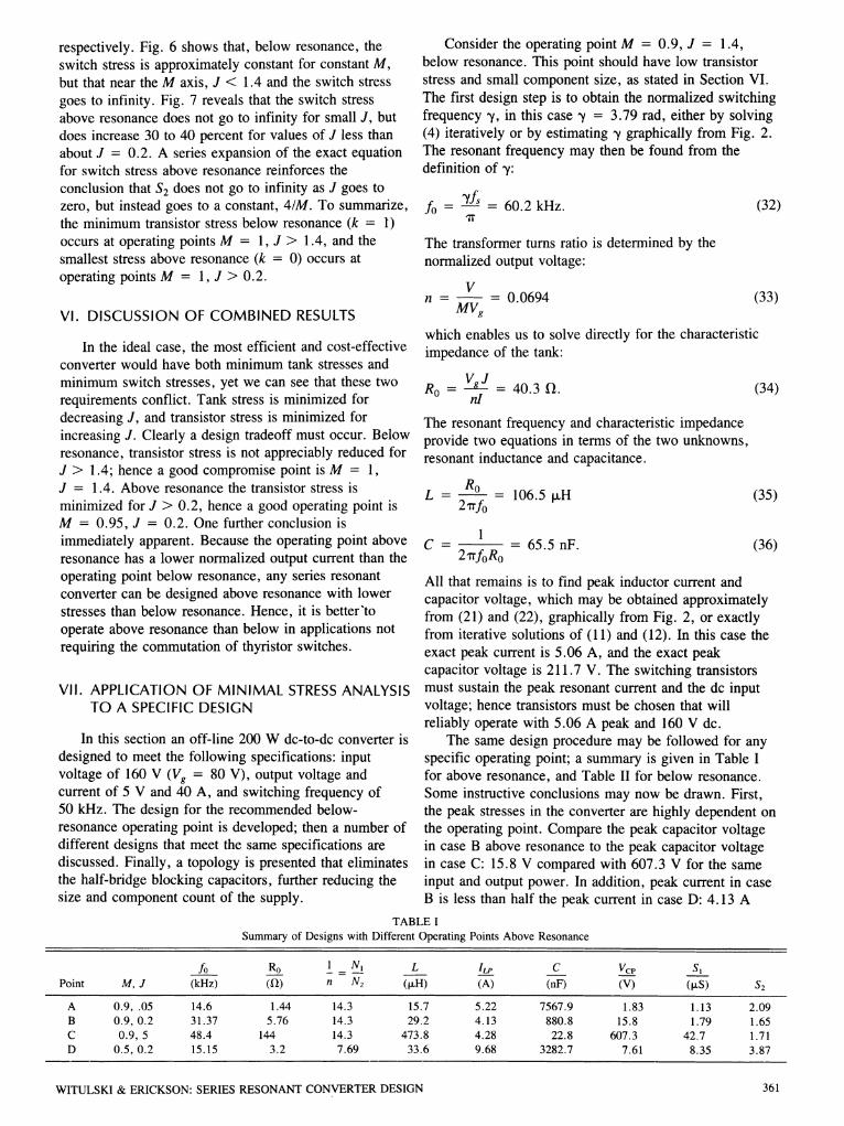
respectively. Fig. 6 shows that, below resonance, theswitch stress is approximately constant for constant M,but that near the M axis, J < 1.4 and the switch stressgoes to infinity. Fig. 7 reveals that the switch stressabove resonance does not go to infinity for small J, butdoes increase 30 to 40 percent for values of J less thanabout J = 0.2. A series expansion of the exact equationfor switch stress above resonance reinforces theconclusion that S2 does not go to infinity as J goes tozero, but instead goes to a constant, 41M. To summarize,the minimum transistor stress below resonance (k = I)occurs at operating points M = 1, J > 1.4, and thesmallest stress above resonance (k = 0) occurs atoperating points M = 1, J > 0.2.
VI. DISCUSSION OF COMBINED RESULTS
In the ideal case, the most efficient and cost-effectiveconverter would have both minimum tank stresses andminimum switch stresses, yet we can see that these tworequirements conflict. Tank stress is minimized fordecreasing J, and transistor stress is minimized forincreasing J. Clearly a design tradeoff must occur. Belowresonance, transistor stress is not appreciably reduced forJ > 1.4; hence a good compromise point is M = 1,J = 1.4. Above resonance the transistor stress isminimized for J > 0.2, hence a good operating point isM = 0.95, J = 0.2. One further conclusion isimmediately apparent. Because the operating point aboveresonance has a lower normalized output current than theoperating point below resonance, any series resonantconverter can be designed above resonance with lowerstresses than below resonance. Hence, it is better tooperate above resonance than below in applications notrequiring the commutation of thyristor switches.
VIl. APPLICATION OF MINIMAL STRESS ANALYSISTO A SPECIFIC DESIGN
In this section an off-line 200 W dc-to-dc converter isdesigned to meet the following specifications: inputvoltage of 160 V (Vg = 80 V), output voltage andcurrent of 5 V and 40 A, and switching frequency of50 kHz. The design for the recommended below-resonance operating point is developed; then a number ofdifferent designs that meet the same specifications arediscussed. Finally, a topology is presented that eliminatesthe half-bridge blocking capacitors, further reducing thesize and component count of the supply.
Consider the operating point M = 0.9, J = 1.4,below resonance. This point should have low transistorstress and small component size, as stated in Section VI.The first design step is to obtain the normalized switchingfrequency -y, in this case y = 3.79 rad, either by solving(4) iteratively or by estimating -y graphically from Fig. 2.The resonant frequency may then be found from thedefinition of y:
(32)fo = =fs= 60.2 kHz.Tr
The transformer turns ratio is determined by thenormalized output voltage:
Vn = ~= 0.0694
MVg~ (33)
which enables us to solve directly for the characteristicimpedance of the tank:
RO = vg = 40.3 QI.nI
The resonant frequency and characteristic impedanceprovide two equations in terms of the two unknowns,resonant inductance and capacitance.
L = ° = 106.5 [H27rfo
1c = ~ = 65.5 nF
2-rrfoRO
(34)
(35)
(36)
All that remains is to find peak inductor current andcapacitor voltage, which may be obtained approximatelyfrom (21) and (22), graphically from Fig. 2, or exactlyfrom iterative solutions of (11) and (12). In this case theexact peak current is 5.06 A, and the exact peakcapacitor voltage is 211.7 V. The switching transistorsmust sustain the peak resonant current and the dc inputvoltage; hence transistors must be chosen that willreliably operate with 5.06 A peak and 160 V dc.
The same design procedure may be followed for anyspecific operating point; a summary is given in Table Ifor above resonance, and Table II for below resonance.Some instructive conclusions may now be drawn. First,the peak stresses in the converter are highly dependent onthe operating point. Compare the peak capacitor voltagein case B above resonance to the peak capacitor voltagein case C: 15.8 V compared with 607.3 V for the sameinput and output power. In addition, peak current in caseB is less than half the peak current in case D: 4.13 A
TABLE ISummary of Designs with Different Operating Points Above Resonance
ff -RO 1 NI L ILP C Vcp S,Point M, J (kHz) (Ql) n N2 (p.H) (A) (nF) (V) (p.S) S2
A 0.9, .05 14.6 1.44 14.3 15.7 5.22 7567.9 1.83 1.13 2.09B 0.9, 0.2 31.37 5.76 14.3 29.2 4.13 880.8 15.8 1.79 1.65C 0.9, 5 48.4 144 14.3 473.8 4.28 22.8 607.3 42.7 1.71D 0.5, 0.2 15.15 3.2 7.69 33.6 9.68 3282.7 7.61 8.35 3.87
WITULSKI & ERICKSON: SERIES RESONANT CONVERTER DESIGN 361

TABLE IISummary of Designs with Different Operating Points Below Resonance
fo RO = N1 L ILP C VCP S,Point M, J (kHz) (fl) n N2 ([iH) (A) (nF) (V) ([IS) S2
A 0.9, 0.9 74.3 25.92 14.3 55.52 6.17 82.6 168.0 11.12 2.47B 0.9, 1.4 60.2 40.3 14.3 106.5 5.06 65.5 211.7 14.16 2.02C 0.9, 5 51.97 144.0 14.3 441.1 4.48 21.3 652.3 44.7 1.79D 0.5, 1.4 65.7 22.4 7.69 54.2 8.55 108.1 231.2 24.3 3.42
compared with 9.46 A. It is clear that the reputation ofthe series resonant converter for high peak stresses isundeserved; it simply must be designed to operate at thecorrect point. Secondly, it is distinctly better to operateabove resonance than below. Compare case B in Table I,the minimal stress point above resonance, with case B inTable II, the minimal stress point below resonance. Thepeak capacitor voltage above resonance is only 15.8 V,or 7.5 percent of the peak voltage below resonance andthe peak resonant current is 4.13 A, or 82 percent of thepeak current at the minimal stress point below resonance.Although the capacitance in this case is larger aboveresonance than below, it is still small (0.88 ,uF) and ismore than compensated for in cost by a smallerinductance (29.2 ,uH compared with 106.5 ,uH). Finally,an inspection of cases A and B in both tables confirmsthe fact that transistor stress increases both above andbelow resonance when normalized output current isdecreased below the minimum stress point.
Before concluding this section on design, it isappropriate to note that the component count of the half-bridge series resonant converter can be reduced. Referringto Fig. 8(a) it can be seen that the entire function of thetwo half-bridge capacitors is to bear the dc component ofthe voltage created by the switching between the inputsource and ground. This dc voltage is dependent entirelyon the duty ratio of the switches, which is alwaysD = 0.5 for a frequency-controlled resonant converter.Hence we may eliminate the half-bridge capacitors bysimply letting the resonant capacitor bear both the ac and
_VC (t) CEB Vg
Vin *1_ < ~~~LC +
CBj-VQ
V-~~~~~~~
Vin
c Vg+Vc(t)
Fig. 8. Three capacitors in half-bridge series resonant converter
(a) can be replaced by single resonant capacitor bearing both ac and dccomponents of capacitor voltage (b).
the dc component of the voltage induced by the switchedinput source, as shown in Fig. 8(b). In this case the peakcapacitor voltage is Vg plus the peak ac component,Vg + Vcp. The cost-effectiveness of this approach willdepend on the tradeoffs involved in a particular designsituation.
VIlI. CONCLUSIONS
If the series resonant converter is to be designedeffectively, there must be a systematic procedure forselecting the characteristic impedance of the tank, RO =
L/C, and the transformer turns ratio n. These twoquantities must be chosen to yield the lowest possiblepeak voltages and currents in the converter for a givenoutput power. In this paper the solution to this problem isfound by normalizing the output voltage and current withrespect to n and RO, then seeking the normalized value ofoutput voltage and current (M, J) that yields the lowestpeak stresses in the general case.
To accomplish this task, two stress functions aredefined to allow measurement of the required size of thecomponents, one for the size of the tank inductor andcapacitor, and one for the transistor switches. Eachfunction is then analyzed to find the normalized outputoperating point that yields the smallest stresses. It isfound that in all cases the component stresses areminimized for large normalized output voltage M nearunity. However, the tank component stress decreases withdecreasing J, and the transistor stress increases fordecreasing J; hence a tradeoff must be made. The bestpoints for combined low stresses appear to be M = 1, J= 1.4 below resonance, and M = 0.95, J = 0.2 aboveresonance.
Application of these results to a design examplereveals that for the same output power, the peak capacitorvoltage can vary by an order of magnitude depending onthe normalized operating point. The peak transistor andinductor currents can be twice as large as necessary if theconverter is not properly designed. Furthermore, it isshown that significantly smaller stresses can be obtainedfor the same converter by operating above resonanceinstead of below. Consequently, in applications notrequiring the commutation of thyristors, it is best tooperate in the above resonance mode.
APPENDIX A. STRESSES IN THE EVENDISCONTINUOUS MODE
As shown in [2], the normalized output voltage in theeven discontinuous mode is
IEEE TRANSACTIONS ON AEROSPACE AND ELECTRONIC SYSTEMS VOL. AES-22, NO. 4 JULY 1986362

k = 2, 4, 6,...
and the circuit equations for peak voltage and current are
Vcp = Vg 2 oY+ (A2)R 0y R 0y
,LP = V; [1 -M + kM]. (A3)RO
Equation (A3) is already in the desired form, and we may
express (A2) in terms ofM by substituting (A1) for theappropriate quantities:
Vcp = VgJ2 + (k - 2)M]. (A4)
Hence, in the discontinuous mode, the peak stresses are
independent of normalized output current and linearlydependent on M, corresponding to vertical lines in theoutput plane. In the discontinuous mode it is the outputvoltage alone that determines when the output bridge isreverse biased: hence determining both the duration andthe charge transferred to the output (magnitude) of theresonant current.
We may now find the stress functions for thediscontinuous mode. In order to find the tank componentstress, substitute (A3) and (A4) into (25):
S2 = (1 + (k - 1)M)2 + (2 - (2 - k)M)2 (A5)fouMJ
for the = 2 discontinuous mode, this reduces to
5 + 2M + M2(AI) S, = 2 >MJ (A6)
Partial differentiation of (A6) demonstrates that the tankcomponent stress in this mode decreases with increasingM and increases with decreasing J, so the operating pointwith minimal tank stress in this mode is at the boundaryM = 1, J = 2/ir. In the same manner the transistorstress function may be found by substitution of (A3) into(28):
= 2(1 + M(k - 1))MJ
(A7)
In this case, the minimum transistor stress occurs at thesame point as the minimum tank component stress, M =
1, J = 2/ir.
REFERENCES
[1] Witulski, A.F., and Erickson, R.W. (1985)Steady-state analysis of the series resonant converter.IEEE Transactions on Aerospace and Electronic Systems,AES-21, 6 (Nov. 1985), 791-799.
[2] Vorperian, V., and Cuk, S. (1982)A complete dc analysis of the series resonant converter.In Record ofIEEE Power Electronics SpecialistsConference, 1982, pp. 269-272.
[3] Steigerwald, R.L. (1984)High frequency resonant dc-dc converters.IEEE Transactions on Industrial Electronics, IE-31, 2 (May1984), 181-191.
Arthur F. Witulski was born in Denver, Colo., on May 27, 1958. He received theB.S. degree in electrical engineering from the University of Colorado, Boulder, in1981.
From 1981 to 1983 he worked in a power electronics group at Storage TechnologyCorporation designing power supplies and associated circuitry for small magnetic tapesubsystems. He is currently studying at the University of Colorado toward a Ph.D.degree in electrical engineering, with primary emphasis in power electronics andcontrol.
Robert W. Erickson(S'81-M'83) was born in Santa Monica, Calif., on August 3,1956. He received the B.S., M.S., and Ph.D. degrees from the California Institute ofTechnology, Pasadena, in 1978, 1980, and 1983, respectively.
He is presently an Assistant Professor in the Department of Electrical andComputer Engineering at the University of Colorado, Boulder. His interests includepower electronics, circuits, and control.
WITULSKI & ERICKSON: SERIES RESONANT CONVERTER DESIGN
M = 2RlR0.y
363