nir spads and fast-gating circuits - issw.epfl.ch · nir spads and fast-gating circuits alberto...
TRANSCRIPT

NIR SPADs and fast-gating circuits
Alberto Tosi and SPADlab colleagues
1st International SPAD Sensor Workshop – ISSW 2018
Les Diablerets, February 26th, 2018
ISSW 2018 – February 26, 2018 – [email protected]
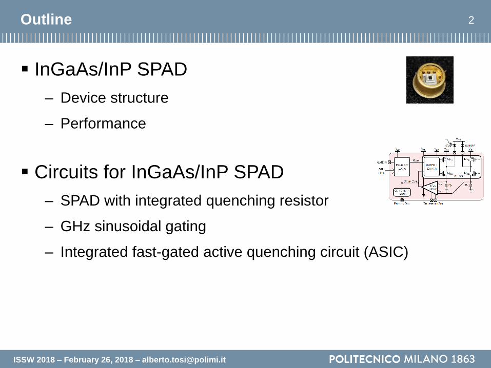
2Outline
InGaAs/InP SPAD
– Device structure
– Performance
Circuits for InGaAs/InP SPAD
– SPAD with integrated quenching resistor
– GHz sinusoidal gating
– Integrated fast-gated active quenching circuit (ASIC)

InGaAs/InP SPAD

ISSW 2018 – February 26, 2018 – [email protected]
4Single-photon counting in the NIR (1 – 1.6 µm)
Quantum Information Processing and Communication
Quantum Key Distribution (QKD)
Eye safe ranging (LIDAR)
Unconventional (ghost, non-line-of-sight, …) imaging
Time-resolved diffused optical spectroscopy
Photodynamic therapy (PDT) for cancer treatment
Optical testing of VLSI circuits
Photonics research in the 1 µm – 1.6 µm range
Detector + electronics tailored for the specific application!
ISSW 2018 – February 26, 2018 – [email protected]
5InGaAs/InP SPAD
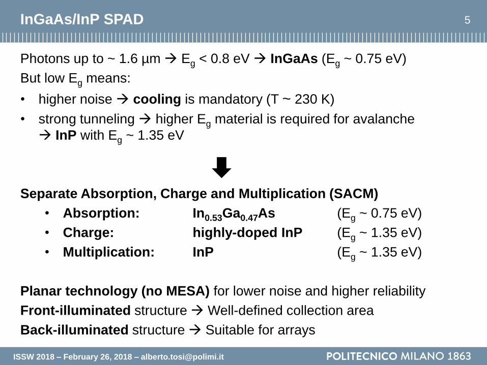
Photons up to ~ 1.6 µm Eg < 0.8 eV InGaAs (Eg ~ 0.75 eV)
But low Eg means:
• higher noise cooling is mandatory (T ~ 230 K)
• strong tunneling higher Eg material is required for avalanche
InP with Eg ~ 1.35 eV
Separate Absorption, Charge and Multiplication (SACM)
• Absorption: In0.53Ga0.47As (Eg ~ 0.75 eV)
• Charge: highly-doped InP (Eg ~ 1.35 eV)
• Multiplication: InP (Eg ~ 1.35 eV)
Planar technology (no MESA) for lower noise and higher reliability
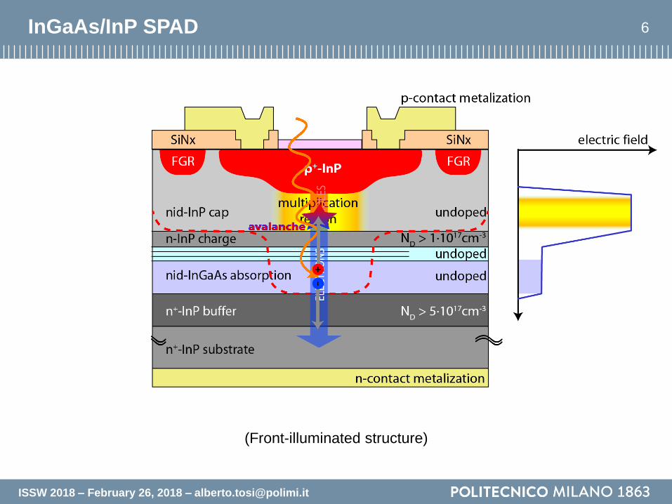
Front-illuminated structure Well-defined collection area
Back-illuminated structure Suitable for arrays
ISSW 2018 – February 26, 2018 – [email protected]
7Design of InGaAs/InP SPAD
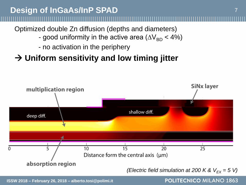
Optimized double Zn diffusion (depths and diameters)
- good uniformity in the active area (∆VBD < 4%)
- no activation in the periphery
Uniform sensitivity and low timing jitter
(Electric field simulation at 200 K & VEX = 5 V)
ISSW 2018 – February 26, 2018 – [email protected]
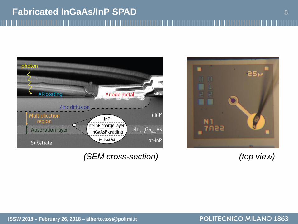
8Fabricated InGaAs/InP SPAD
(SEM cross-section) (top view)

ISSW 2018 – February 26, 2018 – [email protected]
9I-V curve at low temperature
Low dark current: Idark ~ 10 pA @ VBD – 1 V,
sharp breakdown knee, large VBD – VPT difference
0 5 10 15 20 25 30 35 40 45 50 55 60 651f
10f
100f
1p
10p
100p
1n
10n
100n
1µ
10µ
100µ
photocurrent
Temperature = 225 K
Active area diameter = 25 µm
Cu
rre
nt (A
)
Reverse Voltage (V)
dark current
VPT
VBD

ISSW 2018 – February 26, 2018 – [email protected]
10Gated-mode operation
– SPAD is enabled during Gate-ON time
– SPAD is held OFF to empty traps reduce afterpulsing
– Gate period TGATE = TON + TOFF

ISSW 2018 – February 26, 2018 – [email protected]
11Photon detection efficiency
Good photon detection efficiency:
– 40% @ λ = 1000 nm, VEX = 5 V
– 25% @ λ = 1550 nm, VEX = 5 V
– still 3% @ λ = 1700 nm, VEX = 5 V
800 900 1000 1100 1200 1300 1400 1500 1600 17000
5
10
15
20
25
30
35
40
45
VEX
=3V
Ph
oto
n D
ete
cti
on
Eff
icie
nc
y (%
)
Wavelength (nm)
Temp = 200K
VEX
=5V
ISSW 2018 – February 26, 2018 – [email protected]
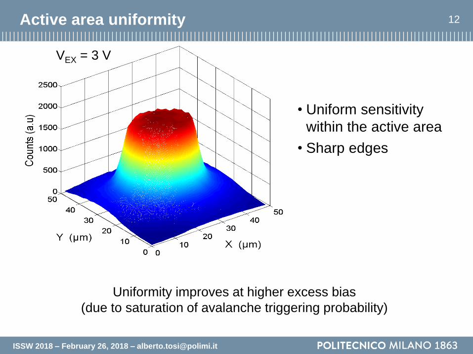
12Active area uniformity
Uniformity improves at higher excess bias
(due to saturation of avalanche triggering probability)
VEX = 3 V
• Uniform sensitivity
within the active area
• Sharp edges

ISSW 2018 – February 26, 2018 – [email protected]
13Low dark-count-rate InGaAs/InP SPAD
0 5 10 15 20 25 30 35 40 45 50 550
5
10
15
20
25
30
Da
rk C
ou
nt
Ra
te (
kc
ps
)
Active area diameter (µm)
SMF 28 pigtailed SPAD
in TO-8 package with DCR ~ 1 kcps
Temperature = 225 K
VEX
= 5 V
• DCR scales with active area bulk origin(while dark current scales with perimeter, i.e. it is peripheral leakage)
• 10 µm InGaAs/InP SPAD with DCR of few kcps
• 10 µm SPADs have been fiber pigtailed (Micro Photon Devices – MPD)
ISSW 2018 – February 26, 2018 – [email protected]
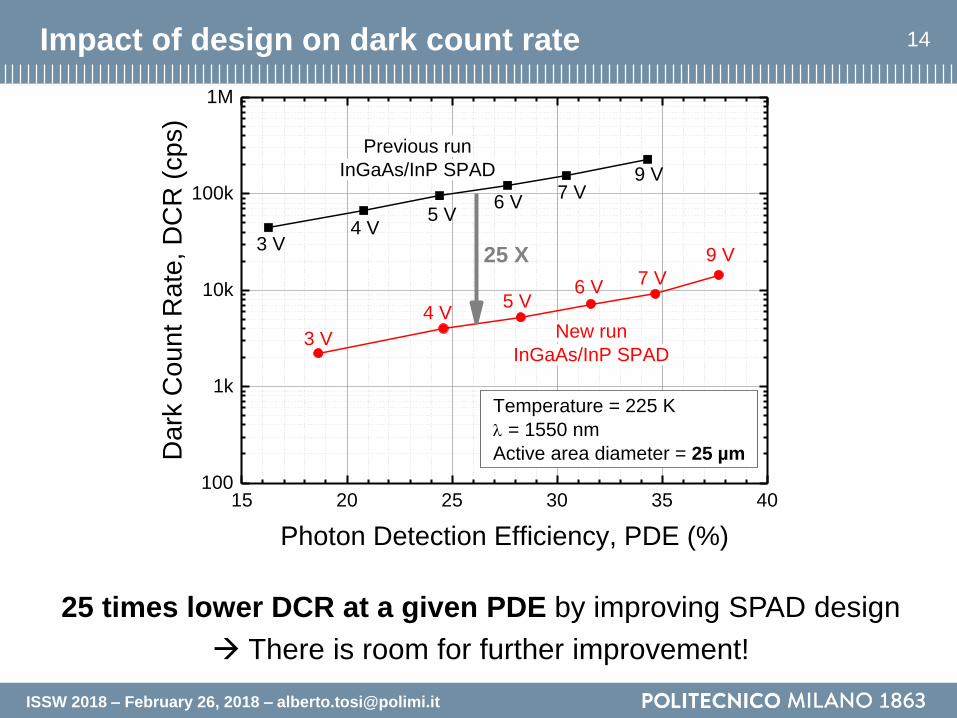
14Impact of design on dark count rate
25 times lower DCR at a given PDE by improving SPAD design
There is room for further improvement!
15 20 25 30 35 40100
1k
10k
100k
1M
3 V4 V
5 V6 V
7 V9 V
9 V
6 V 7 V
5 V4 V
New run
InGaAs/InP SPAD
Temperature = 225 K
= 1550 nm
Active area diameter = 25 µm
Dark
Count R
ate
, D
CR
(cps)
Photon Detection Efficiency, PDE (%)
Previous run
InGaAs/InP SPAD
3 V
25 X
ISSW 2018 – February 26, 2018 – [email protected]
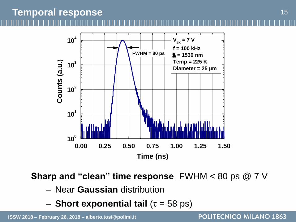
15Temporal response
Sharp and “clean” time response FWHM < 80 ps @ 7 V
– Near Gaussian distribution
– Short exponential tail (τ = 58 ps)
0.00 0.25 0.50 0.75 1.00 1.25 1.5010
0
101
102
103
104
FWHM = 80 ps
Co
un
ts (
a.u
.)
Time (ns)
VEX
= 7 V
f = 100 kHz
= 1530 nm
Temp = 225 K
Diameter = 25 µm
ISSW 2018 – February 26, 2018 – [email protected]
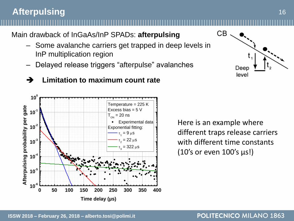
16Afterpulsing
Main drawback of InGaAs/InP SPADs: afterpulsing
– Some avalanche carriers get trapped in deep levels in
InP multiplication region
– Delayed release triggers “afterpulse” avalanches
Limitation to maximum count rate
0 50 100 150 200 250 300 350 40010
-6
10-5
10-4
10-3
10-2
10-1
100
Temperature = 225 K
Excess bias = 5 V
TON
= 20 ns
Experimental data
Exponential fitting:
1 = 9 s
2 = 22 s
3 = 322 s
Aft
erp
uls
ing
pro
bab
ilit
y p
er
gate
Time delay (µs)
Here is an example wheredifferent traps release carrierswith different time constants(10’s or even 100’s µs!)

Circuits for high count rate
InGaAs/InP SPAD systems

ISSW 2018 – February 26, 2018 – [email protected]
18Afterpulsing reduction techniques for higher count rate
Reduce concentration of deep levels
→ challenging task (improved fabrication process)
Long hold-off time before re-arming
→ not an option at high rates
Reduce avalanche carriers
fast quenching (monolithically integrated passive quenching or ASIC)
→ either gated or free-running mode
→ moderately high count rates (1–10 MHz)
short gates (<< 1 ns): → very high (> 100 MHz) count rates
→ complex RF transients suppression
→ non-flat sensitivity
max count rate = 1/Thold-off
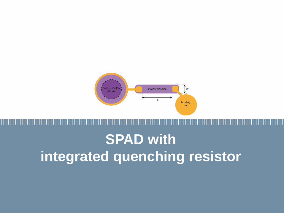
SPAD with
integrated quenching resistor
ISSW 2018 – February 26, 2018 – [email protected]
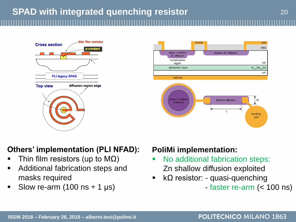
20SPAD with integrated quenching resistor
Others’ implementation (PLI NFAD):
Thin film resistors (up to MΩ)
Additional fabrication steps and
masks required
Slow re-arm (100 ns ÷ 1 μs)
PoliMi implementation:
No additional fabrication steps:
Zn shallow diffusion exploited
kΩ resistor: - quasi-quenching
- faster re-arm (< 100 ns)

ISSW 2018 – February 26, 2018 – [email protected]
21Afterpulsing of InGaAs/InP SPAD with integrated resistor
Significant afterpulsing reduction
1 10 100 100010
3
104
105
106
DC
R (
cp
s)
Hold-off (s)
Temp = 225 K
freq = 1 MHz gate-on = 50 ns
Excess bias = 2.5 V, 5 V, 7 V
InGaAs module with
standard InGaAs/InP SPADs
from the same wafer
InGaAs/InP SPADs with
integrated resistor (L/W = 50)
0.0 0.5 1.0 1.5 2.0 2.5 3.0 3.510
-4
10-3
10-2
10-1
100
VEX
= 3 VVEX
= 5 V
No
rma
lize
d c
ou
nts
(a.u
.)
Time (ns)
Temp = 225 K, = 1550 nm
VEX FWHM
3 V 112 ps
5 V 82 ps
7 V 71 ps
VEX
= 7 V
-10 0 10 20 30 40 50 60 70 80 90 100 110 1200
50
100
150
200
250
300
350
400
VEX
= 5 V
VEX
= 7 V
Co
un
ts (
a.u
.)
Time (ns)
VEX
= 3 V
Temperature = 225 K
L/W = 50 (R ~ 50 k)
RECOVERY
~ 10 ns
Anode recovery transient
Good temporal
response
Faster recovery time
with τ = 10 ns

ISSW 2018 – February 26, 2018 – [email protected]
22Design of a compact module
Detector, front-end electronics and cooling
housed in a small case
• Easy integration in optical setups
• Easy to use and configurable
4 cm
5 cm7 cm

GHz sinusoidal gating with
SPAD-dummy balancing approach
ISSW 2018 – February 26, 2018 – [email protected]
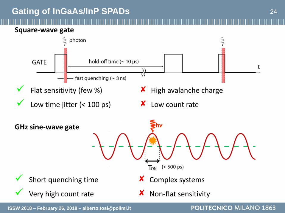
24
Square-wave gate
Flat sensitivity (few %)
Low time jitter (< 100 ps)
High avalanche charge
Low count rate
GHz sine-wave gate
Short quenching time
Very high count rate
Complex systems
Non-flat sensitivity
(< 500 ps)
Gating of InGaAs/InP SPADs

ISSW 2018 – February 26, 2018 – [email protected]
25Gigahertz sinusoidal gating - requirements
Gate signal at fG > 1 GHz for fast avalanche quenching
fG tunable in a wide range (900-1400 MHz) for:
– Synchronization with different external laser systems
– Best trade-off between afterpulsing and detection efficiency
Adjustable excess bias:
– for optimizing PDE, DCR, afterpulsing, timing jitter
– Up to 7 V (27 dBm!)
Long-term stability
– Feedback for gate feed-through rejection
Suitable for rack mounting
TON

ISSW 2018 – February 26, 2018 – [email protected]
26PoliMi “SPAD-dummy” balanced configuration
Detectable avalanche
• SPAD – Dummy couple• Two gate sinusoidal signals in anti-phase for
cancelling capacitive feedthrough• Tunable wideband components
(amplitude matching within 0.1%, phase matching within 0.05°)
VTH
ISSW 2018 – February 26, 2018 – [email protected]
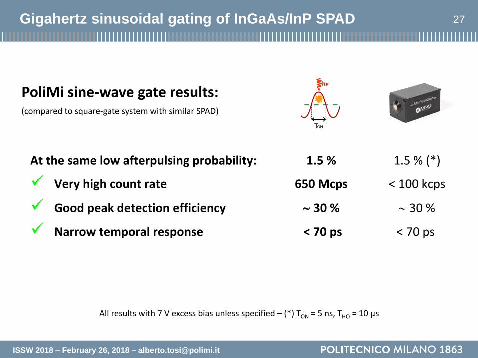
27
At the same low afterpulsing probability: 1.5 % 1.5 % (*)
Very high count rate 650 Mcps < 100 kcps
Good peak detection efficiency 30 % 30 %
Narrow temporal response < 70 ps < 70 ps
All results with 7 V excess bias unless specified – (*) TON = 5 ns, THO = 10 µs
PoliMi sine-wave gate results:(compared to square-gate system with similar SPAD)
Gigahertz sinusoidal gating of InGaAs/InP SPAD

ISSW 2018 – February 26, 2018 – [email protected]
28
-125 -100 -75 -50 -25 0 25 50 75 100 1250
10
20
30 = 1550 nm
VEX
= 7 V
VEX
= 6 V
VEX
= 5 V
VEX
= 4 V
Ph
oto
n D
ete
ctio
n E
ffic
ien
cy (
%)
Time (ps)
10-11
10-10
10-9
10-8
10-7
10-6
10-5
10-4
10-3
10-2
102
103
104
105
106
107
108
109
Co
un
t ra
te (
cp
s)
Input photon flux (a.u.)
Gigahertz sinusoidal gating of InGaAs/InP SPAD
4 5 6 7
0.3
0.5
0.8
1.0
1.3
1.5
Aft
erp
uls
ing
pro
bab
ilit
y (
%)
Excess bias voltage, VEX
(V)
fGATE
= 1.3 GHz
T = 240 K
Afterpulsing probability Linearity
Photon detection efficiency Temporal response
0 1 2 3 4
10
100
1k
10k
100k
VEX
= 7 V
= 1550 nm
Co
un
ts (
cp
s)
Time (ns)
FWHM = 65 ps

ISSW 2018 – February 26, 2018 – [email protected]
29
Main board of the new system:
All the basic blocks on board:
Gate generation
Gate amplification
Avalanche readout
Feedback control system
PLL with multiple outputs generates both gate signals
(800 – 1500 MHz)
Programmable gain amplifier to set gate amplitude (up to VEX = 7 V)
Readout amplifiers with 3 GHz bandwidth and ultrafast comparator
Towards compact gigahertz sinusoidal gating of SPADs

SiGe integrated circuit
for fast gating SPADs
ISSW 2018 – February 26, 2018 – [email protected]
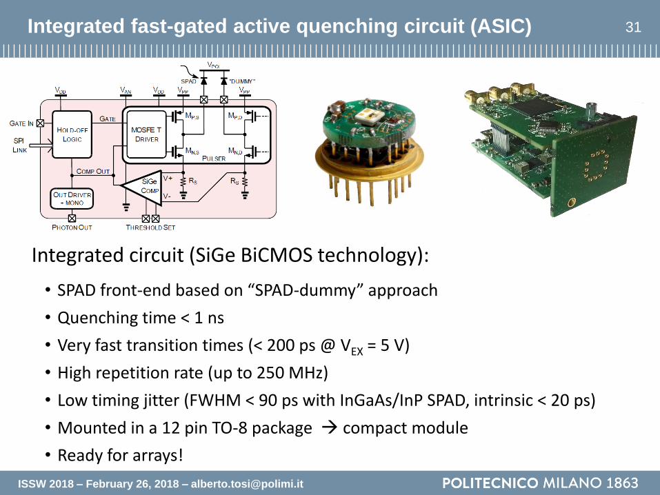
31Integrated fast-gated active quenching circuit (ASIC)
Integrated circuit (SiGe BiCMOS technology):
• SPAD front-end based on “SPAD-dummy” approach
• Quenching time < 1 ns
• Very fast transition times (< 200 ps @ VEX = 5 V)
• High repetition rate (up to 250 MHz)
• Low timing jitter (FWHM < 90 ps with InGaAs/InP SPAD, intrinsic < 20 ps)
• Mounted in a 12 pin TO-8 package compact module
• Ready for arrays!
ISSW 2018 – February 26, 2018 – [email protected]
32
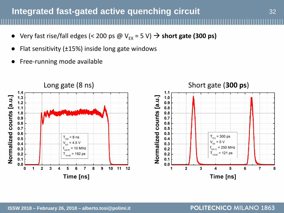
Very fast rise/fall edges (< 200 ps @ VEX = 5 V) short gate (300 ps)
Flat sensitivity (±15%) inside long gate windows
Free-running mode available
Long gate (8 ns) Short gate (300 ps)
Integrated fast-gated active quenching circuit

ISSW 2018 – February 26, 2018 – [email protected]
33Integrated fast-gated active quenching circuit
0 1 2 3 4 5 6 7 8 9 100
20
40
60
80
100
120
140
27 %
Discrete-components module
Fast-gated chip
SP
AD
Curr
en
t (a
.u.)
Time (ns)
VEX
= 5 V
T = 230 K
TON
= 20 ns
100 %
Effective reduction of avalanche charge lower afterpulsing even with long gate
1 10 5010
-5
10-4
10-3
5x10⁻³
Discrete-components module
Fast-gated chip
Afterp
uls
ing p
robabili
ty (
ns
-1)
Time (µs)
VEX
= 5 V
T = 230 K
TON
= 20 ns
5X reduction of afterpulsingwith long gate

ISSW 2018 – February 26, 2018 – [email protected]
34Compact module built around integrated fast-gated chip
Maximum gate repetition rate 250 MHz
Hold-off time 0.003 ÷ 1300 µs
Gate width 0.3 ÷ 1000 ns
SPAD temperature 205 ÷ 290 K
Size 40 x 50 x 70 mm3
Compact module based on integrated circuit & InGaAs/InP SPAD

ISSW 2018 – February 26, 2018 – [email protected]
35Conclusions
InGaAs/InP SPAD:PoliMi experimental results (@ VEX = 5 V):
• Low DCR (~ 103 at 225 K)
• Good detection efficiency (30 % @ 1550 nm)
• Moderately low afterpulsing
• Low timing jitter (FWHM < 90 ps)
Circuits for high-count-rate InGaAs/InP SPAD system:
• SPAD with integrated quenching resistor
• GHz sinusoidal gate (SPAD-dummy balancing approach)
• Very low afterpulsing (< 1.5%)
• High count rate (> 600 Mcount/s)
• Compact modules based on fast-gating ASIC
• Trade-off between standard modules and GHz gating)
Waiting for you at Single Photon Workshop 2019 in Milano!
This work was funded by the projects EMPIR 14IND05 MIQC2 (H2020) and DARPA REVEAL: