nios ii architect design tutorial · 101 innovation drive san jose, ca 95134 tu-01004-2.0 tutorial...
TRANSCRIPT
101 Innovation DriveSan Jose, CA 95134www.altera.com
TU-01004-2.0
Tutorial
Nios II System Architect Design
Document last updated for Altera Complete Design Suite version:Document publication date:
11.0June 2011
Subscribe
Nios II System Architect Design Tutorial

© 2011 Altera Corporation. All rights reserved. ALTERA, ARRIA, CYCLONE, HARDCOPY, MAX, MEGACORE, NIOS, QUARTUS and STRATIX words and logos aretrademarks of Altera Corporation and registered in the U.S. Patent and Trademark Office and in other countries. All other words and logos identified as trademarks or servicemarks are the property of their respective holders as described at www.altera.com/common/legal.html. Altera warrants performance of its semiconductor products to currentspecifications in accordance with Altera's standard warranty, but reserves the right to make changes to any products and services at any time without notice. Altera assumes noresponsibility or liability arising out of the application or use of any information, product, or service described herein except as expressly agreed to in writing by Altera. Alteracustomers are advised to obtain the latest version of device specifications before relying on any published information and before placing orders for products or services.
June 2011 Altera Corporation Nios II System Architect DesignTutorial
June 2011 Altera Corporation
Contents
Chapter 1. Getting StartedHardware and Software Requirements . . . . . . . . . . . . . . . . . . . . . . . . . . . . . . . . . . . . . . . . . . . . . . . . . . . . . 1–1
Acquire the NEEK . . . . . . . . . . . . . . . . . . . . . . . . . . . . . . . . . . . . . . . . . . . . . . . . . . . . . . . . . . . . . . . . . . . . 1–1Install the Design Software . . . . . . . . . . . . . . . . . . . . . . . . . . . . . . . . . . . . . . . . . . . . . . . . . . . . . . . . . . . . . 1–1Install the USB Device Driver . . . . . . . . . . . . . . . . . . . . . . . . . . . . . . . . . . . . . . . . . . . . . . . . . . . . . . . . . . . 1–2Extract the Tutorial Files . . . . . . . . . . . . . . . . . . . . . . . . . . . . . . . . . . . . . . . . . . . . . . . . . . . . . . . . . . . . . . . 1–2
Chapter 2. Designing the SystemDesign Flow . . . . . . . . . . . . . . . . . . . . . . . . . . . . . . . . . . . . . . . . . . . . . . . . . . . . . . . . . . . . . . . . . . . . . . . . . . . . 2–2Design Requirements . . . . . . . . . . . . . . . . . . . . . . . . . . . . . . . . . . . . . . . . . . . . . . . . . . . . . . . . . . . . . . . . . . . . 2–3Design Strategy . . . . . . . . . . . . . . . . . . . . . . . . . . . . . . . . . . . . . . . . . . . . . . . . . . . . . . . . . . . . . . . . . . . . . . . . . 2–4Block Diagram . . . . . . . . . . . . . . . . . . . . . . . . . . . . . . . . . . . . . . . . . . . . . . . . . . . . . . . . . . . . . . . . . . . . . . . . . . 2–6
Chapter 3. Building the Qsys SystemStart Qsys . . . . . . . . . . . . . . . . . . . . . . . . . . . . . . . . . . . . . . . . . . . . . . . . . . . . . . . . . . . . . . . . . . . . . . . . . . . . . . 3–1Specify Qsys System Components . . . . . . . . . . . . . . . . . . . . . . . . . . . . . . . . . . . . . . . . . . . . . . . . . . . . . . . . . 3–2
Add a Nios II Processor to Your System . . . . . . . . . . . . . . . . . . . . . . . . . . . . . . . . . . . . . . . . . . . . . . . . . . 3–3Add a DDR SDRAM Controller . . . . . . . . . . . . . . . . . . . . . . . . . . . . . . . . . . . . . . . . . . . . . . . . . . . . . . . . . 3–5Add a Flash Controller . . . . . . . . . . . . . . . . . . . . . . . . . . . . . . . . . . . . . . . . . . . . . . . . . . . . . . . . . . . . . . . . 3–7Add a Video Subsystem . . . . . . . . . . . . . . . . . . . . . . . . . . . . . . . . . . . . . . . . . . . . . . . . . . . . . . . . . . . . . . . 3–9
Complete the System . . . . . . . . . . . . . . . . . . . . . . . . . . . . . . . . . . . . . . . . . . . . . . . . . . . . . . . . . . . . . . . . . . . . 3–9Specify the External Clocks and Clock Connections . . . . . . . . . . . . . . . . . . . . . . . . . . . . . . . . . . . . . . . 3–10Specify the Reset Connections . . . . . . . . . . . . . . . . . . . . . . . . . . . . . . . . . . . . . . . . . . . . . . . . . . . . . . . . . 3–11Reassign the Component Base Addresses to Eliminate Memory Conflicts . . . . . . . . . . . . . . . . . . . . 3–11Set the Interrupt Priorities . . . . . . . . . . . . . . . . . . . . . . . . . . . . . . . . . . . . . . . . . . . . . . . . . . . . . . . . . . . . . 3–12Set the Arbitration Priorities . . . . . . . . . . . . . . . . . . . . . . . . . . . . . . . . . . . . . . . . . . . . . . . . . . . . . . . . . . . 3–13Specify the Nios II Processor Boot Configuration . . . . . . . . . . . . . . . . . . . . . . . . . . . . . . . . . . . . . . . . . 3–14
Generate the System . . . . . . . . . . . . . . . . . . . . . . . . . . . . . . . . . . . . . . . . . . . . . . . . . . . . . . . . . . . . . . . . . . . . 3–16
Chapter 4. Completing the Quartus II ProjectComplete the Quartus II Project . . . . . . . . . . . . . . . . . . . . . . . . . . . . . . . . . . . . . . . . . . . . . . . . . . . . . . . . . . . 4–1
Add Files to the Quartus II Project . . . . . . . . . . . . . . . . . . . . . . . . . . . . . . . . . . . . . . . . . . . . . . . . . . . . . . . 4–1Add the Pin Assignments . . . . . . . . . . . . . . . . . . . . . . . . . . . . . . . . . . . . . . . . . . . . . . . . . . . . . . . . . . . . . . 4–2Compile Your Design . . . . . . . . . . . . . . . . . . . . . . . . . . . . . . . . . . . . . . . . . . . . . . . . . . . . . . . . . . . . . . . . . . 4–2
Configure the FPGA . . . . . . . . . . . . . . . . . . . . . . . . . . . . . . . . . . . . . . . . . . . . . . . . . . . . . . . . . . . . . . . . . . . . . 4–3
Chapter 5. Creating the Software ApplicationCreate a New BSP Project . . . . . . . . . . . . . . . . . . . . . . . . . . . . . . . . . . . . . . . . . . . . . . . . . . . . . . . . . . . . . . . . . 5–1Create a New Software Project . . . . . . . . . . . . . . . . . . . . . . . . . . . . . . . . . . . . . . . . . . . . . . . . . . . . . . . . . . . . 5–2Add Source Code Files to the Project . . . . . . . . . . . . . . . . . . . . . . . . . . . . . . . . . . . . . . . . . . . . . . . . . . . . . . . 5–3Configure the BSP Properties . . . . . . . . . . . . . . . . . . . . . . . . . . . . . . . . . . . . . . . . . . . . . . . . . . . . . . . . . . . . . 5–4Specify the Zip File System Settings . . . . . . . . . . . . . . . . . . . . . . . . . . . . . . . . . . . . . . . . . . . . . . . . . . . . . . . . 5–6Build the Software Project . . . . . . . . . . . . . . . . . . . . . . . . . . . . . . . . . . . . . . . . . . . . . . . . . . . . . . . . . . . . . . . . 5–7Program the Zip File to Flash Memory . . . . . . . . . . . . . . . . . . . . . . . . . . . . . . . . . . . . . . . . . . . . . . . . . . . . . 5–8Run the Software Application on the NEEK . . . . . . . . . . . . . . . . . . . . . . . . . . . . . . . . . . . . . . . . . . . . . . . . . 5–9Console Output . . . . . . . . . . . . . . . . . . . . . . . . . . . . . . . . . . . . . . . . . . . . . . . . . . . . . . . . . . . . . . . . . . . . . . . . 5–10Interact with the Software Application . . . . . . . . . . . . . . . . . . . . . . . . . . . . . . . . . . . . . . . . . . . . . . . . . . . . 5–10Booting from Flash Memory . . . . . . . . . . . . . . . . . . . . . . . . . . . . . . . . . . . . . . . . . . . . . . . . . . . . . . . . . . . . . 5–10
Nios II System Architect DesignTutorial

iv Contents
Additional InformationTaking the Next Step . . . . . . . . . . . . . . . . . . . . . . . . . . . . . . . . . . . . . . . . . . . . . . . . . . . . . . . . . . . . . . . . . . Info–1Document Revision History . . . . . . . . . . . . . . . . . . . . . . . . . . . . . . . . . . . . . . . . . . . . . . . . . . . . . . . . . . . Info–2How to Contact Altera . . . . . . . . . . . . . . . . . . . . . . . . . . . . . . . . . . . . . . . . . . . . . . . . . . . . . . . . . . . . . . . . Info–2Typographic Conventions . . . . . . . . . . . . . . . . . . . . . . . . . . . . . . . . . . . . . . . . . . . . . . . . . . . . . . . . . . . . . Info–2
Nios II System Architect Design June 2011 Altera CorporationTutorial

June 2011 Altera Corporation
1. Getting Started
This tutorial teaches you how to use the Quartus® II software and the Nios® II Embedded Design Suite (EDS) to implement a digital picture viewer in a Cyclone III FPGA. In this tutorial, you build a processor-based hardware system in programmable logic for the Nios II Embedded Evaluation Kit, Cyclone® III Edition (NEEK) and run software on it. The tutorial demonstrates the steps to build complete, complex embedded designs using the Altera® design software.
1 You must use the specified spelling for names of files, components, and other objects, for the tutorial design to function correctly with the software provided. For example, the software application refers to hardware components by the names specified in this tutorial. If you name a component differently, the software application does not identify it correctly.
Hardware and Software RequirementsThis tutorial requires the following hardware and software:
■ NEEK development board
■ Quartus II software v11.0, including the following items:
■ Quartus II FPGA synthesis and compilation tool
■ Qsys system integration tool
■ MegaCore IP library
■ Nios II EDS, featuring the Nios II Software Build Tools (SBT) for Eclipse™
■ Design files for this tutorial
The following sections describe the setup and installation steps. After completing the setup and installation requirements, you are ready to create your first system-level design.
Acquire the NEEKYou can purchase the NEEK by following the instructions on the Nios II Embedded Evaluation Kit, Cyclone III Edition page of the Altera website.
Install the Design SoftwareDownload and install the subscription edition or the web edition of the Quartus II software from Download Center page of the Altera website.
f For information about installing the Quartus II software, refer to the Altera Software Installation and Licensing Manual.
Nios II System Architect DesignTutorial

1–2 Chapter 1: Getting StartedHardware and Software Requirements
Install the USB Device DriverAfter the software is installed, you can connect the NEEK board to the USB port on your PC. If the software prompts you to install the USB Blaster driver, install it from the following location: <Altera software installation directory>\11.0\quartus\drivers\usb-blaster. If the driver is not located in this directory, install the appropriate version for your system from the Cable & Adapter Drivers Information page of the Altera website.
f For additional information, refer to the USB-Blaster Download Cable User Guide.
Extract the Tutorial FilesThe tutorial files are available for download as a compressed zip file (.zip) from the Nios II System Architect Design page or adjacent to this tutorial on the literature pages of the Altera website. When you extract the files from this .zip, you must ensure that the directory path on your PC contains only folder names with no spaces in them. The directory in which you unzip the tutorial files is your <working directory>.
Nios II System Architect Design June 2011 Altera CorporationTutorial

June 2011 Altera Corporation
2. Designing the System
To architect a system, you specify the design requirements and develop a suitable design strategy to address each requirement. Design requirements include immediate design goals of the product and features to keep your product commercially successful in the future. You must consider desired application functionality, cost, flexibility to add future features, time to market, and obsolescence.
Programmable logic solutions provide optimal flexibility in your architecture to add features over time quickly and at low cost. For example, a programmable logic solution enables you to add features such as graphics or video display to a commercial implementation of the digital picture viewer quickly and cheaply. Programmable logic solutions allow you to integrate all the parts of the design on a single low-cost, low-power programmable logic device. They support short time to market, and insulate your design from part obsolescence — the potential lack of future support for specific microprocessors, LCD panels, LCD controllers, and flash memory devices, for example — by providing the ability to migrate your design to another device without extensive modification.
Therefore, this tutorial implements the digital picture viewer on a programmable logic platform using Altera’s Qsys system integration tool.
Product design goals originate in customer requirements and become inputs to system definition. System definition is the first step in the design process.
The following sections describe the Altera design flow for an embedded system, the design requirements for the digital picture viewer design you implement in this tutorial, the design strategies that dictate the decisions about the hardware components in the implemented design, and the basic system description for the digital picture viewer. By explaining the design flow, design requirements, and design strategy in this chapter, this chapter teaches you the system architecture of the digital picture viewer.
Nios II System Architect DesignTutorial
2–2 Chapter 2: Designing the SystemDesign Flow
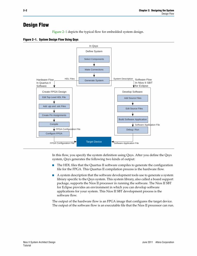
Design FlowFigure 2–1 depicts the typical flow for embedded system design.
In this flow, you specify the system definition using Qsys. After you define the Qsys system, Qsys generates the following two kinds of output:
■ The HDL files that the Quartus II software compiles to generate the configuration file for the FPGA. This Quartus II compilation process is the hardware flow.
■ A system description that the software development tools use to generate a system library specific to the Qsys system. This system library, also called a board support package, supports the Nios II processor in running the software. The Nios II SBT for Eclipse provides an environment in which you can develop software applications for your system. This Nios II SBT development process is the software flow.
The output of the hardware flow is an FPGA image that configures the target device. The output of the software flow is an executable file that the Nios II processor can run.
Figure 2–1. System Design Flow Using Qsys
Generate System
Make Connections
Select Components
Define System
In Qsys
Hardware FlowIn Quartus IISoftware
Compile
Configure FPGA
Debug / Run
Create Pin Assignments
Edit Top-Level HDL File
Add .qip and .sdc Files
Software FlowIn Nios II SBTfor Eclipse
Build Software Application
Edit Source Files
Add Source Files
Create FPGA Design Develop Software
System DescriptionHDL Files
FPGA Configuration File
FPGA Configuration File
Software Application File
Software Application FileTarget Device
Nios II System Architect Design June 2011 Altera CorporationTutorial

Chapter 2: Designing the System 2–3Design Requirements
In this tutorial you perform the following steps:
1. Build a Qsys system:
a. Open the Quartus II project.
b. Start Qsys.
c. Select and configure system components, including IP MegaCore functions.
d. Make connections.
e. Assign clocks and set base addresses.
f. Set interrupt and arbitration priorities.
2. Generate the system to create the following items:
■ HDL for the entire Qsys system
■ A system description file that software development tools use to build the hardware drivers and other relevant system information for the software application
3. Complete the Quartus II project:
a. Add the Qsys system to the top level of the Quartus II project.
b. Add pin assignments.
c. Compile the project to generate an SRAM Object File (.sof).
d. Use the Quartus II Programmer to download the .sof to the FPGA.
4. Develop the software application:
a. Start the Nios II SBT for Eclipse.
b. Add source files.
c. Configure build properties.
d. Build the application to generate the Executable and Linking Format File (.elf).
5. Use the Flash Programmer to convert the image files to flash memory image files (.flash) and download the flash image data to CFI flash memory.
6. Use the Nios II SBT for Eclipse to download and run the .elf for the software application.
Each major step of the design process is described in a tutorial chapter.
Design RequirementsIn this tutorial, you design a digital picture viewer that allows a user to view pictures stored in JPEG format and to scroll through JPEG pictures stored in the external flash memory, using the LCD touch-screen display.
June 2011 Altera Corporation Nios II System Architect DesignTutorial
2–4 Chapter 2: Designing the SystemDesign Strategy
Design StrategyQsys provides standard hardware components that you can add to your system. You can add several instances of each component. The only restriction is the resources available on your board to implement all of the components you instantiate in your design.
The NEEK comprises a Cyclone III FPGA Starter Board and an LCD Multimedia High Speed Mezzanine Card (HSMC) daughtercard in addition to accessories and software. The following NEEK hardware resources are required to run the design you create in this tutorial:
■ The following Cyclone III FPGA Starter Board resources are required:
■ Cyclone III EP3C25F324 FPGA
■ Embedded USB-Blaster™ circuitry (including an Altera EPM3128A CPLD) allowing download of FPGA configuration files through your PC’s USB port
■ 256-Mbit DDR SDRAM
■ 1 MByte of synchronous SRAM
■ 16 MBytes of Intel P30/P33 flash memory
■ 50-MHz on-board oscillator
■ The following LCD daughtercard resources are required:
■ LCD touch-screen 800 × 480 pixel display
■ 10-bit VGA digital access card
The NEEK has additional features, including additional memory, not required to implement this design.
The Qsys system contains both control path and data path components. The Nios II processor is the main system controller. It initializes and calibrates the LCD controller, intercepts user touch input, and initializes the data path. It communicates with other control path components through Avalon Memory-Mapped (Avalon-MM) interface ports.The Nios II processor reads the program code from DDR SDRAM memory, and the DDR SDRAM also holds the video frame buffer. A tristate conduit bridge component connects the flash controller with the off-chip flash memory.
The Nios II processor sends frame buffer data from the DDR SDRAM to a video pipeline of specialized Avalon Streaming (Avalon-ST) components that move and process the pixel data, converting it to video data signals and sending them to the LCD screen.
The pixels must be rendered on the LCD screen smoothly and without delays. This design achieves this goal by running the DDR SDRAM at a high clock rate to improve the performance of the video frame buffer.
Nios II System Architect Design June 2011 Altera CorporationTutorial

Chapter 2: Designing the System 2–5Design Strategy
Table 2–1 shows how the individual design requirements for this project are implemented by specific design strategies, which in turn dictate the components you add to your system in this tutorial.
f The implementation of the video pipeline and the touch screen controller are described in more detail in Implementing an LCD Controller and the Nios II 3C25 Microprocessor with LCD Controller Data Sheet.
Table 2–1. Standard Hardware Components to Implement the Digital Picture Viewer Requirements
Design Requirement Design Strategy Components Needed
Display JPEG pictures on the LCD Display■ LCD screen controller
■ A video pipeline to send video data to the LCD screen
■ PIO
■ Video pipeline peripherals
Scroll through JPEG pictures■ An interrupt to capture touch screen
events
■ Touch screen control
■ PIO
■ SPI
Frame buffering
■ Need a large memory. Use the on-board DDR SDRAM
■ Transfer video data from memory to Video pipeline
■ DDR SDRAM controller
■ SGDMA
Store JPEG images, FPGA configuration file, application software, and reset vectors in a nonvolatile memory
Use the on-board flash memory Flash controller
Store program code, stack, and exception vectors Use the onboard DDR SDRAM DDR SDRAM controller
Generate interrupts and measure system performance Need a timer Interval timer
Download, run, and debug software JTAG UART communication interfaces JTAG UART
Keep track of hardware and software builds
Ensure software is only run on the hardware for which it was compiled System ID peripheral
June 2011 Altera Corporation Nios II System Architect DesignTutorial

2–6 Chapter 2: Designing the SystemBlock Diagram
Block DiagramFigure 2–2 shows a high-level block diagram of the system you develop to implement the design.
As systems get larger and more complicated, it is easier to design at a higher level of abstraction using—and reusing—customized HDL components, which may include IP cores, verification IP and other design modules. Qsys automatically generates the system interconnect fabric, which is the glue logic that connects the design blocks together. The system interconnect fabric manages design issues such as dynamic bus-width matching, interrupt priorities, and arbitration.
f For additional information about the Altera system interconnect fabric, refer to Avalon Interface Specifications.
Qsys supports hierarchical system design, which means you can instantiate a system as a component in a higher-level system. This approach allows you to divide a large design into smaller subsystems, which are easier to manage and control. You can also promote design reuse by reusing these subsystems with minimal changes in your other designs. In this tutorial, the video pipeline components are grouped in the video subsystem and low-frequency components such as the PIO and SPI components are grouped in the peripheral subsystem.
f For additional information about Qsys, refer to the Qsys System Integration Tool page of the Altera website.
Figure 2–2. High-Level Block Diagram of Digital Picture Viewer
Video Subsystem
CFI FlashController
TristateConduit Bridge
SystemID
Nios II/fProcessor
To LCD
Peripheral Subsystem
To Flash Memory
To SDRAM To LCD ControllerTo Touch Screen
LCDDAT PIO
IRQPIO
SPI LCDCLK PIO
LCDEN PIO
System Interconnect Fabric
JTAGUART
SystemTimer
EEPROMCLK PIO
EEPROMDATA PIO
To EEPROM
DDR SDRAMController
Timing Adatper 0SG-DMA
PixelFIFO
DataFormatAdapter
VideoSync
Generator
Timing Adatper 1
PixelConverter
Nios II System Architect Design June 2011 Altera CorporationTutorial

June 2011 Altera Corporation
3. Building the Qsys System
In this chapter, you add components to the system, make connections where required, assign the clocks, set arbitration priorities, and generate the system.
The tutorial combines various components and subsystems to create a Qsys complete system. The video subsystem and peripheral subsystem are also complete Qsys systems, which you add to your top level system.
The following Qsys files are provided in the tutorial folder:
■ main_system.qsys—A partially-completed, top-level Qsys system, to which you add a Nios II embedded processor, a DDR SDRAM controller, a flash controller, and a video subsystem.
■ video_system.qsys—A completed Qsys system that contains the video pipeline components.
■ peripheral_system.qsys—A completed Qsys system that contains the low-frequency peripherals.
After you add the components to the top-level system, you must perform some additional steps to create the .sof that you use to configure the FPGA. All of the necessary steps are described in this chapter.
If you wish to skip the steps to create the .sof, you can use the completed design available in your <working directory>/complete_system folder and skip to Chapter 4, Completing the Quartus II Project.
Start QsysTo run Qsys, perform the following steps:
1. Run the Quartus II software. On your Windows system, click Start > All Programs > Altera > Quartus II <version>.
2. On the File menu, click Open Project.
3. Browse to locate <working directory>/tutorial/sys_arc_lab.qpf. The Quartus II project for the tutorial opens. Ignore the error messages referring to the unconnected components. You connect the components later in this tutorial.
4. On the Tools menu, click Qsys. Qsys opens.
5. On the File menu, click Open and browse to locate the top-level Qsys file, <working directory>/tutorial/main_system.qsys. Qsys loads a partial system. In the following section, you add the remaining components to the system.
1 For main_system.qsys, Qsys displays the subsystems as single components. To view the subsystem details, start another Qsys instance and open <working directory>/tutorial/video_subsystem.qsys or peripheral_system.qsys.
Nios II System Architect DesignTutorial

3–2 Chapter 3: Building the Qsys SystemSpecify Qsys System Components
Specify Qsys System ComponentsTable 3–1 shows the components of the completed design, including components in the subsystems.
1 Ignore the error messages that appear in the Qsys message console. The steps in “Complete the System” on page 3–9 resolve these errors.
Table 3–1. Components in the Partial Qsys System
Component Component Instance Name Component Role
Nios II Processor cpu Runs the software that controls the system.
Generic Tri-State Controller flash
Controls the timing for driving read and write transactions on the external CFI flash memory. The CFI flash memory device stores the JPEG images for the picture viewer application.
Tri-State Conduit Bridge flash_bridge Connects the flash memory controller to the external flash memory.
DDR SDRAM Controller with ALTMEMPHY
ddr_sdram Stores execute code and data in the frame buffers.
System ID sysid Allows the Nios II_SBT to verify that the software is built for the correct hardware version.
Avalon-MM Clock Crossing Bridge slow_clock_crossing_bridge Connects the processor in the high-frequency domain to the
slower-frequency peripherals.
PIO (Parallel I/O) lcd_i2c_scl LCD controller interface components. The three-wire interface includes a data signal, a clock signal, and an enable signal. Refer to Implementing an LCD Controller.
PIO (Parallel I/O) lcd_i2c_en
PIO (Parallel I/O) lcd_i2c_sdat
PIO (Parallel I/O) pio_id_eeprom_scl Two-wire EEPROM ID interface components. The I2C serial EEPROM ID chip stores information about the board, including the touch screen calibration data.PIO (Parallel I/O) pio_id_eeprom_dat
SPI (3 Wire Serial) touch_panel_spi Touch screen interface components. Refer to Implementing an LCD Controller.PIO (Parallel I/O) touch_panel_pen_irq_n
JTAG UART jtag_uart Enables software to access a debug serial port.
Interval timer sys_clk_timer Enables software to perform periodic interrupts for maintenance and to maintain software application timing requirements.
Scatter-Gather DMA Controller sgdma Controls the video pipeline components.
Avalon-ST Timing Adapter timer_adapter_0
Video pipeline components. Refer to Implementing an LCD Controller.
On-Chip Memory fifo
Avalon-ST Timing Adapter timer_adapter_1
Pixel Converter(BGR0 -> BGR) pixel_converter
Avalon-ST Data Format Adapter data_format_adapter
Video Sync Generator video_sync_generator
Nios II System Architect Design June 2011 Altera CorporationTutorial

Chapter 3: Building the Qsys System 3–3Specify Qsys System Components
This section shows you how to perform the following actions:
1. Add a Nios II Processor to Your System.
2. Add a DDR SDRAM Controller.
3. Add a Flash Controller.
4. Add a Video Subsystem.
1 Altera recommends that you save your work after you add each component. To save the current Qsys system, on the File menu, click Save.
Add a Nios II Processor to Your SystemYour system requires a CPU to run the software application that controls the tutorial demo. To add a Nios II embedded processor to your system, perform the following steps:
1. On the Component Library tab, expand Processors, and double-click Nios II Processor.
1 Alternatively, you can use the search box on the Component Library tab to locate components in the library.
June 2011 Altera Corporation Nios II System Architect DesignTutorial

3–4 Chapter 3: Building the Qsys SystemSpecify Qsys System Components
2. Select the Nios II/f processor. Figure 3–1 shows the Nios II Processor parameter editor after you select the Nios II/f core.
3. Click Finish.
4. In the Module Name column on the System Contents tab, right-click the new Nios II processor name, click Rename, and type cpu to rename the new component.
5. In the connection panel, connect the data_master port of cpu to the control_slave port of sysid and the slow_clock_crossing_bridge_s0 port of peripheral_subsystem.
1 To make a connection, click on the intersection of each pair of relevant signal lines. A solid dot represent a connection; an open dot indicates the two signals are not connected.
Figure 3–1. Nios II Processor Component Settings
Nios II System Architect Design June 2011 Altera CorporationTutorial

Chapter 3: Building the Qsys System 3–5Specify Qsys System Components
Figure 3–2 shows the connection panel with the data_master port of cpu correctly connected.
Add a DDR SDRAM ControllerYour system requires a large, fast memory block to store executable code and the video frame buffers. To give your system access to the on-board DDR SDRAM, perform the following steps to add a DDR SDRAM controller to your system:
1. On the Component Library tab, expand Memories and Memory Controllers, expand External Memory Interfaces, expand Memory Interfaces, expand DDR, and double-click DDR SDRAM Controller with ALTMEMPHY.
2. On the Memory Settings page, update the following parameters:
a. For Speed grade, select the correct speed grade for your device. This tutorial assumes speed grade 6.
b. For PLL reference clock frequency MHz, type 50.
c. For Memory clock frequency MHz, type 100.
d. For Controller data rate, select Full.
e. Under Memory Presets, scroll and click PSC A2S56D40CTP-G5 to match the DDR SDRAM on the NEEK.
f. Click Modify parameters.
g. In the Parameters table, scroll to locate RAS to RAS delay time (tRRD).
h. In the Value cell for the parameter, type 11.0. For a memory interface clock frequency of 100 MHz, the minimum tRRD requirement is 11.0 ns.
i. Click OK.
Figure 3–2. Qsys Connection Panel
June 2011 Altera Corporation Nios II System Architect DesignTutorial
3–6 Chapter 3: Building the Qsys SystemSpecify Qsys System Components
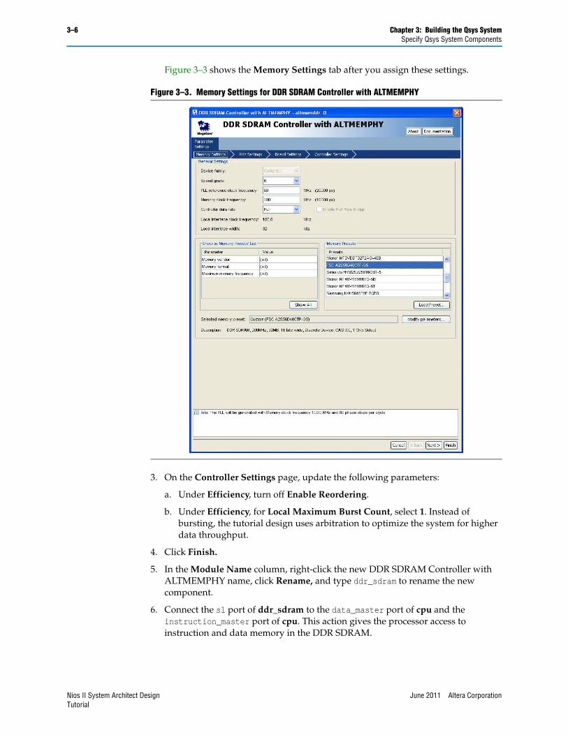
Figure 3–3 shows the Memory Settings tab after you assign these settings.
3. On the Controller Settings page, update the following parameters:
a. Under Efficiency, turn off Enable Reordering.
b. Under Efficiency, for Local Maximum Burst Count, select 1. Instead of bursting, the tutorial design uses arbitration to optimize the system for higher data throughput.
4. Click Finish.
5. In the Module Name column, right-click the new DDR SDRAM Controller with ALTMEMPHY name, click Rename, and type ddr_sdram to rename the new component.
6. Connect the s1 port of ddr_sdram to the data_master port of cpu and the instruction_master port of cpu. This action gives the processor access to instruction and data memory in the DDR SDRAM.
Figure 3–3. Memory Settings for DDR SDRAM Controller with ALTMEMPHY
Nios II System Architect Design June 2011 Altera CorporationTutorial

Chapter 3: Building the Qsys System 3–7Specify Qsys System Components
7. In the Export column, click Click to export and set the following ddr_sdram signal rows to the following names:
■ For external_connection, type ddr_sdram_external_connection.
■ For memory, type ddr_sdram_memory.
■ For auxfull, type ddr_sdram_auxfull.
Figure 3–4 shows the exported connections.
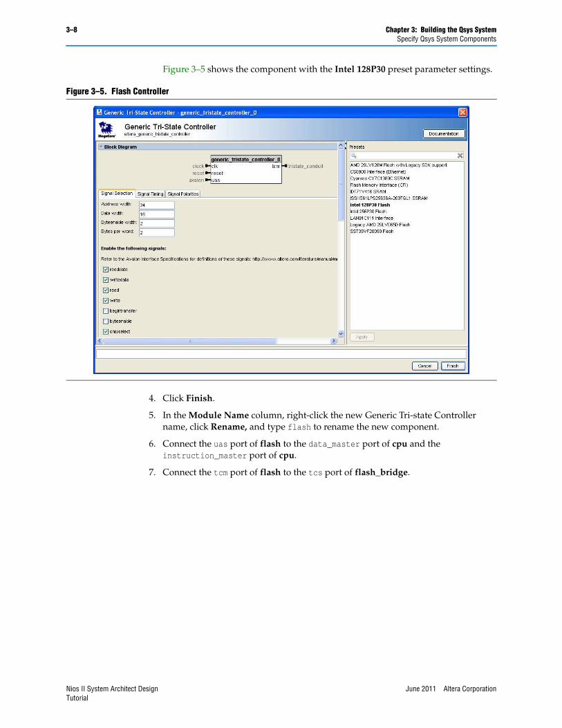
Add a Flash ControllerTo use the Generic Tri-state Controller component as a flash controller, perform the following steps:
1. On the Component Library tab, expand Tri-State Components and double-click Generic Tri-State Controller.
2. In the Presets list, select Intel 128P30.
3. Click Apply.
Figure 3–4. Exported DDR SDRAM Connections
June 2011 Altera Corporation Nios II System Architect DesignTutorial
3–8 Chapter 3: Building the Qsys SystemSpecify Qsys System Components
Figure 3–5 shows the component with the Intel 128P30 preset parameter settings.
4. Click Finish.
5. In the Module Name column, right-click the new Generic Tri-state Controller name, click Rename, and type flash to rename the new component.
6. Connect the uas port of flash to the data_master port of cpu and the instruction_master port of cpu.
7. Connect the tcm port of flash to the tcs port of flash_bridge.
Figure 3–5. Flash Controller
Nios II System Architect Design June 2011 Altera CorporationTutorial

Chapter 3: Building the Qsys System 3–9Complete the System
Add a Video SubsystemThe video subsystem consists of the video pipeline components. To add a video subsystem to your system, perform the following steps:
1. On the Component Library tab, expand System and double-click video_system.
Figure 3–6 shows the video subsystem that you extracted from the tutorial’s .zip file earlier.
2. Click Finish.
3. In the Module Name column, right-click the new video system name, click Rename, and type video_subsystem to rename the new component.
4. Connect the sgdma_csr port of video_subsystem to the data_master port of cpu to give the processor access to the SGDMA in the video subsystem.
5. Connect the s1 port of ddr_sdram to the sgdma_descriptor_read port of video_subsystem, the sgdma_descriptor_write port of video_subsystem, and the sgdma_m_read port of video_subsystem.
6. In the Export column, Click to export and type lcd_video_interface in the video_subsystem video_interface signal row.
After you perform these instructions, the Qsys system contains all required components. Next, you complete the system design and resolve the system validation errors.
Complete the SystemThis section shows you how to complete your Qsys system and ensure the components work together correctly. It contains the instructions that show you how to perform the following actions:
1. Specify the External Clocks and Clock Connections.
2. Reassign the Component Base Addresses to Eliminate Memory Conflicts.
3. Set the Interrupt Priorities.
4. Set the Arbitration Priorities.
Figure 3–6. Video Subsystem
June 2011 Altera Corporation Nios II System Architect DesignTutorial
3–10 Chapter 3: Building the Qsys SystemComplete the System
5. Specify the Nios II Processor Boot Configuration.
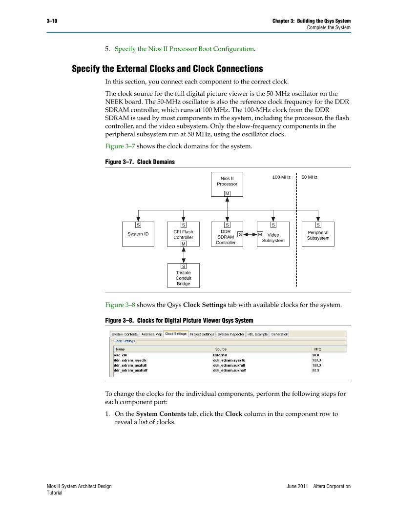
Specify the External Clocks and Clock ConnectionsIn this section, you connect each component to the correct clock.
The clock source for the full digital picture viewer is the 50-MHz oscillator on the NEEK board. The 50-MHz oscillator is also the reference clock frequency for the DDR SDRAM controller, which runs at 100 MHz. The 100-MHz clock from the DDR SDRAM is used by most components in the system, including the processor, the flash controller, and the video subsystem. Only the slow-frequency components in the peripheral subsystem run at 50 MHz, using the oscillator clock.
Figure 3–7 shows the clock domains for the system.
Figure 3–8 shows the Qsys Clock Settings tab with available clocks for the system.
To change the clocks for the individual components, perform the following steps for each component port:
1. On the System Contents tab, click the Clock column in the component row to reveal a list of clocks.
Figure 3–7. Clock Domains
Figure 3–8. Clocks for Digital Picture Viewer Qsys System
DDRSDRAM
Controller
Nios IIProcessor
S
S
M
CFI FlashController
TristateConduitBridge
S
S
M
System ID
S
PeripheralSubsystem
S
VideoSubsystem
S
M
100 MHz 50 MHz
Nios II System Architect Design June 2011 Altera CorporationTutorial

Chapter 3: Building the Qsys System 3–11Complete the System
2. Select the desired clock name according to Table 3–2.
Table 3–2 lists the clocks for the different component ports. For each clock, components are listed in the order they appear in the Qsys System Contents tab.
Specify the Reset ConnectionsThis design has a single reset coming into the Qsys system, namely, the clk_reset port of osc_clk. Connect the components in the system to this main reset by clicking on the connection dot between the clk_reset port of osc_clk and the following component ports:
■ The reset port of flash_bridge
■ The reset_50 port of peripheral_subsystem
■ The reset_100 port of peripheral_subsystem
■ The reset port of sysid
■ The reset_n port of cpu
■ The soft_reset_n port of ddr_sdram
■ The global_reset_n port of ddr_sdram
■ The reset port of flash
■ The reset_n port of video_subsystem
Reassign the Component Base Addresses to Eliminate Memory ConflictsTo reassign component base addresses to eliminate undesired overlap between the address spaces of different components, perform the following steps:
1. On the System menu, click Assign Base Addresses. Qsys assigns appropriate base addresses for the components.
Table 3–2. Clocks for Individual Components in Digital Picture Viewer Qsys System
Clock Name Frequency Source Component/Port
osc_clk 50 MHz Oscillator ddr_sdram / refclk
ddr_sdram_sysclk 100 MHz SDRAM PLL
■ flash_bridge / clk
■ peripheral_subsystem / clk_100
■ sysid / clk
■ cpu / clk
■ flash / clk
■ video_subsystem / clk_100
June 2011 Altera Corporation Nios II System Architect DesignTutorial

3–12 Chapter 3: Building the Qsys SystemComplete the System
2. Reassign the following base addresses to the Avalon Memory-Mapped (Avalon-MM) slave ports of the following components:
■ For the jtag_debug_module port of cpu, type 0x1000000.
■ For the uas port of flash, type 0x00000000.
■ For the s1 port of ddr_sdram, type 0x2000000.
■ For the sgdma_csr port of video_subsystem, type 0x5000000.
■ For the slow_clock_crosing_bridge port of peripheral_subsystem, type 0x4000000.
■ For the control_slave port of sysid, type 0x1000800.
3. To view the address map for the system, click the Address Map tab.
Set the Interrupt PrioritiesTo render images on the LCD screen smoothly, the sgdma component of the video subsystem must continuously service the frame buffer without stalling. When the sgdma component completes a transaction, it must be updated immediately by the Nios II processor. Therefore, sgdma must have the highest interrupt priority, followed by the timer, jtag_uart, and touch-screen components. The lowest interrupt value indicates the highest interrupt priority. Assign interrupt priorities to the system components by performing the following steps for each interrupt-request (IRQ) port listed in Table 3–3:
1. Click the System Contents tab.
2. On the left edge of the System Contents tab, click the filter icon. The Filters dialog box appears.
3. In the Filter list, select All Interfaces.
4. Close the Filters dialog box.
5. For each port specified in Table 3–3, perform the following steps:
a. In the IRQ column, double-click the connection dot.
b. Type the interrupt priority value from Table 3–3.
Figure 3–9. Base Address Setting Conflict that Requires Manual Reassignment
Table 3–3. Interrupt Priority Assignments (Part 1 of 2)
Component Port Interrupt Priority Value
video_subsystem sgdma_csr_irq 2
peripheral_subsystem sys_clk_timer_irq 8
peripheral_subsystem jtag_uart_irq 10
Nios II System Architect Design June 2011 Altera CorporationTutorial

Chapter 3: Building the Qsys System 3–13Complete the System
Figure 3–10 shows the related peripheral_subsystem component ports after you perform this step.
Set the Arbitration PrioritiesTo ensure that the video pipeline operates smoothly, you must assign the highest arbitration priority to sgdma accesses to ddr_sdram. In addition, because the heap memory is located in DDR SDRAM, you must increase the arbitration priority of the Nios II processor for ddr_sdram to support more back-to-back data transactions.
To assign arbitration priorities among the components in your system, perform the following steps:
1. Right-click anywhere on the System Contents tab, and click Show Arbitration Shares. The connection panel displays the arbitration priority of each master for each slave to which it is connected. By default, Qsys assigns arbitration priority 1 for each connected master-slave pair.
2. For each master-slave connection in Table 3–4, double-click the box that represents the connection and type the new value from the table.
peripheral_subsystem touch_panel_pen_irq_n 14
peripheral_subsystem touch_panel_spi_irq 16
Table 3–3. Interrupt Priority Assignments (Part 2 of 2)
Component Port Interrupt Priority Value
Figure 3–10. Interrupt Request Priority of lcd_sgdma Component
Table 3–4. Arbitration Priority Assignments
Master Port Slave Port Arbitration Priority
video_subsystem / sgdma_m_read ddr_sdram / s1 50
video_subsystem / sgdma_descriptor_write ddr_sdram / s1 8
video_subsystem / sgdma_descriptor_read ddr_sdram / s1 8
June 2011 Altera Corporation Nios II System Architect DesignTutorial

3–14 Chapter 3: Building the Qsys SystemComplete the System
Figure 3–11 shows the arbitration values after you make the assignments.
3. To hide the arbitration priorities, right-click anywhere on the System Contents tab, and click Show Arbitration Shares.
Specify the Nios II Processor Boot ConfigurationImmediately after completing its hardware reset sequence, the Nios II processor begins executing software located at a predefined memory location. The reset vector specifies this location.
1 Altera recommends that your reset vector specify a nonvolatile memory location.
When a software exception or interrupt event occurs, the Nios II processor begins executing software in another predefined location.The exception vector specifies this location.
To set the reset and exception vectors for the Nios II processor in your system, perform the following steps:
1. In the Module Name column, double-click cpu. The Nios II processor parameter editor appears.
2. In the Reset Vector Memory list, select flash.uas.
3. In the Reset Vector Offset box, type 0x100000.
4. In the Exception Vector Memory list, select ddr_sdram.s1.
Figure 3–11. Arbitration Priorities in Digital Picture Viewer Qsys System
Nios II System Architect Design June 2011 Altera CorporationTutorial

Chapter 3: Building the Qsys System 3–15Complete the System
5. In the Exception Vector Offset box, type 0x20.
Figure 3–12 shows the Nios II Processor parameter editor after you perform these steps.
6. Click Finish.
Your Qsys system content is complete and you can now generate the Qsys system.
Figure 3–12. Nios II Processor Reset and Exception Vector Settings
June 2011 Altera Corporation Nios II System Architect DesignTutorial

3–16 Chapter 3: Building the Qsys SystemGenerate the System
Figure 3–13 shows the finalized Qsys system.
Generate the SystemAfter you verify that all the component names in your Qsys system match the component names in Figure 3–13, you are ready to generate your system.
To generate your Qsys system, perform the following steps:
Figure 3–13. Final Digital Picture Viewer Qsys System
Nios II System Architect Design June 2011 Altera CorporationTutorial

Chapter 3: Building the Qsys System 3–17Generate the System
1. On the Generation tab, click the Generate button. The Generate dialog box appears, displaying generation messages as generation proceeds.
As shown in Figure 2–1 on page 2–2, Qsys creates the following output items:
■ HDL files for the components in your system
■ HDL files for the system interconnect to connect the components together
■ System description used by the software development tool, the Nios II SBT for Eclipse, to build the software project
After your system generates successfully, the following message appears:
Generate completed.
2. Click Close.
June 2011 Altera Corporation Nios II System Architect DesignTutorial

3–18 Chapter 3: Building the Qsys SystemGenerate the System
Nios II System Architect Design June 2011 Altera CorporationTutorial

June 2011 Altera Corporation
4. Completing the Quartus II Project
In this chapter, you complete the Quartus II project by adding the top-level HDL file, which instantiates the Qsys system, adding the timing constraints file, and setting the pin assignments. You compile your project in the Quartus II software to perform analysis, synthesis, fitting, and timing analysis. Compilation generates an FPGA image as a .sof file. After you download the FPGA image to the NEEK, the on-board FPGA functions as a processor custom-made for your application.
1 If you wish to work with the completed project provided with the tutorial files, click Open Project on the Quartus II software File menu, browse to locate <working directory>/complete_system/sys_arc_lab.qpf, then skip directly to “Configure the FPGA” on page 4–3.
Complete the Quartus II ProjectThis section teaches you how to complete your Quartus II project. It contains the instructions that show you how to perform the following actions:
1. Add Files to the Quartus II Project
2. Add the Pin Assignments
3. Compile Your Design
Add Files to the Quartus II ProjectTo add files from Qsys to your Quartus II project, perform the following steps:
1. In the Quartus II software, on the File Menu, click Open Project.
2. Browse to locate <working directory>/tutorial/sys_arc_lab.qpf.
3. On the Project menu, click the Add/Remove Files in Project.
4. Verify the following files are included in the project:
■ main_system.qip—The Quartus II IP File (.qip), which contains information from Qsys system generation
■ sys_arc_lab_top_level.v—The top-level wrapper file, which instantiates the main_system.qsys system
■ sys_arc_lab.sdc—The Synopsys Design Constraints File (.sdc), which contains timing constraints for the top-level system
Nios II System Architect DesignTutorial

4–2 Chapter 4: Completing the Quartus II ProjectComplete the Quartus II Project
Figure 4–1 shows the files included in the project.
Add the Pin AssignmentsTo add the pin assignments to your Quartus II project, perform the following steps:
1. On the Assignments menu, click Pin Planner.
2. For each row in the pin table, double-click the Location column cell and select the desired pin. For this project, all pins are already assigned.
Figure 4–2 shows the pin planner.
3. Close the pin planner.
Compile Your DesignTo compile your design, perform the following steps:
1. On the Processing menu, click Start Compilation.
The Quartus II software requires a few minutes to compile the design. Completion percentages update in the Tasks view as compilation proceeds. The design should compile without errors.
Figure 4–1. Quartus II Project Files
Figure 4–2. Qsys System Inserted in Top-Level Project
Nios II System Architect Design June 2011 Altera CorporationTutorial

Chapter 4: Completing the Quartus II Project 4–3Configure the FPGA
2. When compilation completes, click OK to close the Full Compilation was successful message.
Compilation produces the .sof file, <working directory>/tutorial/sys_arc_lab.sof.
Configure the FPGANext, use the Quartus II Programmer to download the .sof to the NEEK and configure the Cyclone III device on the board.
f For more information about the Quartus II Programmer, refer to the Quartus II Programmer chapter in volume 3 of the Quartus II Handbook.
To configure the FPGA, perform the following steps:
1. On the Tools menu, click Programmer.
2. Ensure that the power switch (SW1) on the back side of the NEEK is in the OFF position (up).
3. Connect the USB cable from your PC to the NEEK.
4. Connect the power cable to the NEEK.
5. Press the power switch to turn on the NEEK.
6. In the Quartus II Programmer, click Hardware Setup.
7. Under Currently selected hardware, click USB-Blaster [USB-0].
8. Click Close.
9. Click Auto Detect. The Device column lists the EP3C25F324 device on your board, indicating that the Quartus II Programmer detected the device. Figure 4–3 shows the Quartus II Programmer after you perform this step.
Figure 4–3. Quartus II Programmer
June 2011 Altera Corporation Nios II System Architect DesignTutorial

4–4 Chapter 4: Completing the Quartus II ProjectConfigure the FPGA
10. If your .sof does not appear in the Quartus II Programmer, perform the following steps:
a. Click Add File.
b. Browse to locate <working directory>/tutorial/sys_arc_lab.sof.
c. Click Open.
11. Turn on Program/Configure for your .sof.
12. Click Start to program the FPGA.
After the Programmer completes programming the FPGA, the progress bar reaches 100%, and no error messages appear.
After you complete all the steps in this chapter, you have successfully compiled and downloaded the FPGA image to the Cyclone III device on your NEEK. The processor is ready to run. Next, you must develop the software application and download it to the NEEK.
Nios II System Architect Design June 2011 Altera CorporationTutorial

June 2011 Altera Corporation
5. Creating the Software Application
In this chapter, you use the Nios II SBT for Eclipse to develop the software application that runs on your system. You create a new software application project, a board support package (BSP) for your project (to provide a software runtime environment customized for the hardware system defined in the previous chapter), add the software source files to the project, configure the project, and build the project. The result of the build process is an .elf file. The Nios II SBT for Eclipse downloads the application .elf to the memory location at which the Nios II processor expects to find the executable program. The Nios II processor then runs the application .elf.
f For more information about the Nios II SBT for Eclipse, refer to the Getting Started with the Graphical User Interface chapter of the Nios II Software Developer’s Handbook and to the Developing Nios II Software chapter of the Embedded Design Handbook.
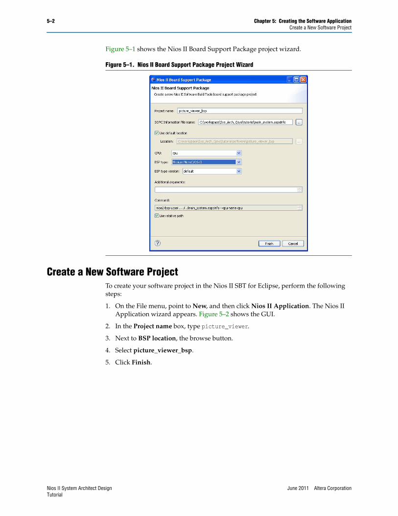
Create a New BSP ProjectTo create the BSP project in the Nios II SBT for Eclipse, perform the following steps:
1. Start the Nios II SBT for Eclipse. On Windows computers, click Start, point to Programs, Altera, Nios II EDS <version>, and then click Nios II <version> Software Build Tools for Eclipse. On Linux computers, run the executable file <Nios II EDS install path>/bin/eclipse-nios2.
2. If the Workspace Launcher dialog box appears, click OK to accept the default workspace location.
3. On the File menu, point to New, and then click Nios II Board Support Package. The Nios II Board Support Package wizard appears. Figure 5–1 shows the GUI.
4. In the Project name box, type picture_viewer_bsp.
5. Next to SOPC Information File name, browse to locate <working directory>/tutorial/main_system.sopcinfo.
6. In the BSP type list, select Micrium MicroC/OS-II.
7. Click Finish.
Nios II System Architect DesignTutorial
5–2 Chapter 5: Creating the Software ApplicationCreate a New Software Project
Figure 5–1 shows the Nios II Board Support Package project wizard.
Create a New Software ProjectTo create your software project in the Nios II SBT for Eclipse, perform the following steps:
1. On the File menu, point to New, and then click Nios II Application. The Nios II Application wizard appears. Figure 5–2 shows the GUI.
2. In the Project name box, type picture_viewer.
3. Next to BSP location, the browse button.
4. Select picture_viewer_bsp.
5. Click Finish.
Figure 5–1. Nios II Board Support Package Project Wizard
Nios II System Architect Design June 2011 Altera CorporationTutorial

Chapter 5: Creating the Software Application 5–3Add Source Code Files to the Project
Figure 5–2 shows the New Project dialog box after you perform these steps.
Add Source Code Files to the ProjectYour working directory contains a software_source_files folder. The files in this folder are the source code files for the tutorial software application project.
To copy these files to the software application folder, perform the following steps:
1. In an application such as Windows Explorer, open the <working directory>/software_source_files folder and select all the folders and files.
2. Drag the files and drop them on the picture_viewer folder in the Project Explorer view of the Nios II SBT for Eclipse. The File and Folder Operation dialog box appears.
3. Select Copy files and folders and click OK.
Figure 5–2. New Application Project Wizard
June 2011 Altera Corporation Nios II System Architect DesignTutorial

5–4 Chapter 5: Creating the Software ApplicationConfigure the BSP Properties
4. Right-click the picture_viewer folder, and click Refresh.
The files copy to the software project directory, and their names appear in the Nios II SBT for Eclipse as shown in Figure 5–3.
Configure the BSP PropertiesIn this section, you configure the BSP to specify the properties of this software system. BSP properties include the interface for stdio and stderr messages, the memory in which to allocate the stack and the heap, and whether an operating system or network stack should be included in the project image. Most of the BSP properties have default settings you do not need to change.
To configure the BSP properties, perform the following steps:
1. In the Project Explorer view, right-click picture_viewer_bsp, point to Nios II, and click BSP Editor. The Nios II BSP Editor opens.
2. On the Main tab, select peripheral_subsystem_jtag_uart for stderr, stdin, and stdout.
Figure 5–3. Software Application Project with Source Code Files
Nios II System Architect Design June 2011 Altera CorporationTutorial
Chapter 5: Creating the Software Application 5–5Configure the BSP Properties
3. For sys_clk_timer, select peripheral_subsystem_sys_clk_timer.
Figure 5–4 shows the settings for the Nios II BSP Editor Main tab.
Figure 5–4. BSP Settings for BSP Editor Main Tab
June 2011 Altera Corporation Nios II System Architect DesignTutorial
5–6 Chapter 5: Creating the Software ApplicationSpecify the Zip File System Settings
4. On the Linker Script tab, for each enabled row in the Linker Section Mappings table, select ddr_sdram in the Linker Region Name column.
Figure 5–5 shows the settings for the Nios II BSP Editor Linker Script tab.
5. On the File menu, click Save.
6. Click Exit to close the Nios II BSP Editor.
Specify the Zip File System SettingsThe tutorial software application project manipulates stored JPEG images. These JPEG images are stored in the CFI flash memory on the NEEK. The project uses the Altera read-only zip file system to store and access the JPEG images in flash memory.
To use the read-only zip file system, you must ensure that the JPEG image files are zipped in a single file in uncompressed mode. The tutorial design files include a prezipped, uncompressed file that contains the JPEG image files.
To add the Altera read-only zip file system and set up your project to store the prezipped JPEG images to the NEEK flash memory, perform the following steps:
1. In an application such as Windows Explorer, open the <working directory> folder and select jpeg_images.zip.
2. Drag and drop jpeg_images.zip on the picture_viewer_bsp folder in the Project Explorer view of the Nios II SBT for Eclipse. The File Operation dialog box appears.
3. Select Copy files and click OK. The file copies to the BSP project directory and appears in the Nios II SBT for Eclipse.
Figure 5–5. BSP Settings for BSP Editor Linker Script Tab
Nios II System Architect Design June 2011 Altera CorporationTutorial

Chapter 5: Creating the Software Application 5–7Build the Software Project
4. Right-click picture_viewer_bsp, point to Nios II, and click BSP Editor.
5. On the Software Packages tab, in the Enable column, turn on altera_ro_zipfs. The altera_ro_zipfs parameters appear.
6. For ro_zipfs_base, type 0x00000000, which is the base address of in the hardware system.
7. For ro_zipfs_name, type /mnt/rozipfs, which is the mount point to use to access the .jpg files.
8. For ro_zipfs_offset, type 0x400000, which is the start address of the location in flash where the .jpg files will be stored.
Figure 5–5 shows the settings for the Nios II BSP Editor Linker Script tab.
9. On the File menu, click Save.
10. Click Generate. An updated BSP is generated.
11. Click Exit to close the Nios II BSP Editor.
f For more information about the Altera read-only zip file system, refer to the Read-Only Zip File System chapter of the Nios II Software Developer’s Handbook.
Build the Software ProjectTo compile and build the image files for your software project, perform the following steps:
1. In the Project Explorer view, right-click picture_viewer, and click Build Project.
The Nios II SBT for Eclipse compiles the BSP and application software projects. The result of the compilation process is an .elf file.
1 If you are prompted to regenerate the BSP, right click picture_viewer_bsp and click Regenerate BSP, then repeat step 1.
Figure 5–6. Altera Read-Only Zip File System Settings for Digital Picture Viewer
June 2011 Altera Corporation Nios II System Architect DesignTutorial
5–8 Chapter 5: Creating the Software ApplicationProgram the Zip File to Flash Memory
Program the Zip File to Flash MemoryYou use the Flash Programmer to convert the .zip file to a Motorola S record file (.flash) and program the .flash file to the flash memory on the NEEK.
To convert the .zip file and program the flash memory, perform the following steps:
1. In the Nios II SBT for Eclipse, on the Nios II menu, click Flash Programmer. The Nios II Flash Programmer appears.
2. In the Nios II Flash Programmer, on the File menu, click New. The New Nios II Flash Programmer Settings File dialog box appears.
3. Select Get flash programmer system details from BSP Settings File.
4. In the BSP Settings File name box, browse to locate <working directory>/tutorial/software/picture_viewer_bsp/settings.bsp.
5. Click OK.
6. On the Flash: flash tab, click Add. The Select Files for Flash Conversion dialog box appears.
7. In the Files of type list, select All Files.
8. Browse to locate <working directory>/tutorial/software/picture_viewer_bsp/jpeg_images.zip.
9. Under Files for flash conversion, double-click in the Flash Offset column.
10. In the Flash Offset box, type 0x400000.
11. Click Start. A new Nios II Flash Programmer Settings File (.flash-settings) is created and flash memory is programmed.
1 If you encounter errors during flash programming, repeat the steps in “Configure the FPGA” on page 4–3 to reconfigure the board with the .sof file, then repeat step 11.
12. Click Exit to close the Nios II Flash Programmer.
Nios II System Architect Design June 2011 Altera CorporationTutorial

Chapter 5: Creating the Software Application 5–9Run the Software Application on the NEEK
Figure 5–7 shows the Nios II Flash Programmer after completing the steps.
f For more information about the Flash Programmer, refer to the Nios II Flash Programmer User Guide.
Run the Software Application on the NEEKRunning an application on the target hardware requires the following two image files:
■ FPGA hardware image—.sof
■ Software executable image—.elf
In Chapter 4, Completing the Quartus II Project, you configured the FPGA by downloading the .sof to the FPGA. After you configure the FPGA, it is ready to run the software application. You download the application through the USB cable that remains plugged in to the NEEK board.
To run the software project on the Nios II processor you configured on the NEEK, perform the following steps:
1. In the Project Explorer view, right-click picture_viewer.
2. Click Run As > Nios II Hardware.
Figure 5–7. Flash Programmer Settings to Program Flash Memory With JPEG Images .zip File
June 2011 Altera Corporation Nios II System Architect DesignTutorial
5–10 Chapter 5: Creating the Software ApplicationConsole Output
3. If the Run Configurations dialog box appears, perform the following steps:
a. On the Target Connection tab, click Refresh Connections and Apply until a board connection establishes.
b. Click Run.
The Run or Run As command rebuilds the software project to create an up–to-date executable and then download the code to memory. The debugger resets the Nios II processor, and the Nios II processor then executes the downloaded code.
Console OutputAfter the application begins executing, it relays messages to the Nios II SBT for Eclipse through the JTAG interface. Figure 5–8 shows the output in the Nios II view.
Interact with the Software ApplicationWhen the picture_viewer application starts running on the Nios II processor, the digital picture viewer displays the first JPEG image. To display the next image, press the Forward button on the LCD touch screen. To display the previous image, press the Back button on the LCD touch screen. Two small thumbnail images on the bottom of the screen display the decoding status of the previous and next images.
Congratulations! You have successfully completed the embedded systems tutorial.
1 The Nios II Flash Programmer overwrites the default application selector on the NEEK. To restore the factory image, refer to the "Restoring the Factory Image" appendix in the Nios II Embedded Evaluation Kit, Cyclone III Edition User Guide.
Booting from Flash MemoryTo boot from the flash memory, you need to program the flash memory with the .sof and .elf files. You use the Nios II Flash Programmer to convert the .sof and .elf files to .flash format and program the .flash files into flash memory.
To convert the files and program the flash memory, perform the following steps:
1. On the Nios II menu, click Flash Programmer. The Nios II Flash Programmer appears.
Figure 5–8. Output from Successful Run of Digital Picture Viewer
Nios II System Architect Design June 2011 Altera CorporationTutorial

Chapter 5: Creating the Software Application 5–11Booting from Flash Memory
2. On the File menu, click New. The New Flash Programmer Settings Files dialog box appears.
3. Select Get flash programmer system details from BSP Settings File.
4. In the BSP Settings File name box, browse to locate <working directory>/tutorial/software/picture_viewer_bsp/settings.bsp.
5. Click OK.
6. To convert and program the .sof, perform the following steps:
a. On the Flash: flash tab, click Add. The Select Files for Flash Conversion dialog box appears.
b. In the Files of type list, select Quartus II SOF File.
c. Browse to locate <working directory>/tutorial/sys_arc_lab.sof.
d. Under Files for flash conversion, double-click in the Flash Offset column.
e. In the Flash Offset box, type 0x20000.
f. Next to the File generation command box, click Properties.
g. In the Additional arguments box, type --activeparallel.
h. Click Close.
7. To convert and program the .elf, perform the following steps:
a. On the Flash: flash tab, click Add. The Select Files for Flash Conversion dialog box appears.
b. In the Files of type list, select Nios II ELF File.
c. Browse to locate <working directory>/tutorial/software/picture_viewer/picture_viewer.elf.
8. Click Start. A new Nios II Flash Programmer Settings File (.flash-settings) is created and flash memory is programmed. Programming might take a few minutes.
1 If you encounter errors during flash programming, repeat the steps in “Configure the FPGA” on page 4–3 to reconfigure the board with the .sof file, then repeat step 8.
9. Click Exit to close the Nios II Flash Programmer.
10. After flash programming is done, power cycle the NEEK to run the picture viewer.
June 2011 Altera Corporation Nios II System Architect DesignTutorial

5–12 Chapter 5: Creating the Software ApplicationBooting from Flash Memory
Figure 5–9 shows the Nios II Flash Programmer after completing the steps.
Figure 5–9. Flash Programmer Settings to Boot from Flash Memory
Nios II System Architect Design June 2011 Altera CorporationTutorial

June 2011 Altera Corporation
Additional Information
This chapter provides additional information about the document and Altera.
Taking the Next StepAltera offers many resources to help you get started designing your own embedded designs. If you are starting from scratch, Altera recommends that you purchase an Altera development kit.
If you already have a working project, you can add a Qsys system to your top-level project as a stub or add your design to the Qsys system as a custom component.
f The following documents and web pages provide information to help you create custom components for your Qsys system:
■ The System Design with Qsys section of Volume 1: Design and Synthesis of the Quartus II Handbook provides complete reference on using Qsys, including topics such as building memory subsystems, creating custom components, and automatically generating interconnect fabric based on a network-on-a-chip topology.
■ Avalon Memory-Mapped Master Templates web page describes how to use an Avalon-MM template to create an Avalon-MM custom component.
■ Avalon Memory-Mapped Slave Template web page describes how to use an Avalon-MM template to create an Avalon-MM slave custom component.
■ Guidelines for Developing a Nios II HAL Device Driver describes how to develop software device drivers for your custom component.
f The following Altera documents and web pages provide background and general information about building embedded systems using Altera tools:
Subject Information Source
Altera embedded solutions Processors from Altera and Embedded Alliance Partners web page
Embedded IP peripherals Embedded Peripherals IP User Guide
Embedded system design Embedded Design Handbook
Evaluation and development kits Development Kits, Daughter Cards & Programming Hardware web page
Nios II processor Nios II Processor Reference Handbook
Nios II processor system design examples and software applications Nios II Embedded Processor Design Examples web page
Nios II software development tools Nios II Software Developer’s Handbook
Nios II user communityAltera Forum website
Altera Wiki website
Nios II System Architect DesignTutorial

Info–2 Additional InformationDocument Revision History
Document Revision HistoryThe following table shows the revision history for this document.
How to Contact AlteraTo locate the most up-to-date information about Altera products, refer to the following table.
Typographic ConventionsThe following table shows the typographic conventions this document uses.
Online tutorials and in-person training
Embedded HW Designer Curriculum web page
Embedded SW Designer Curriculum web page
Qsys System Design with Qsys section of Volume 1: Design and Synthesis of the Quartus II Handbook
Subject Information Source
Date Version Changes
June 2011 2.0 Updated for Qsys and the Nios II Software Build Tools for Eclipse.
May 2009 1.0 Initial release.
Contact (1) Contact Method Address
Technical support Website www.altera.com/support
Technical trainingWebsite www.altera.com/training
Email [email protected]
Product literature Website www.altera.com/literature
Nontechnical support (general) Email [email protected]
(software licensing) Email [email protected]
Note to Table:
(1) You can also contact your local Altera sales office or sales representative.
Visual Cue Meaning
Bold Type with Initial Capital Letters
Indicate command names, dialog box titles, dialog box options, and other GUI labels. For example, Save As dialog box. For GUI elements, capitalization matches the GUI.
bold typeIndicates directory names, project names, disk drive names, file names, file name extensions, software utility names, and GUI labels. For example, \qdesigns directory, D: drive, and chiptrip.gdf file.
Italic Type with Initial Capital Letters Indicate document titles. For example, Stratix IV Design Guidelines.
italic typeIndicates variables. For example, n + 1.
Variable names are enclosed in angle brackets (< >). For example, <file name> and <project name>.pof file.
Nios II System Architect Design June 2011 Altera CorporationTutorial

Additional Information Info–3Typographic Conventions
Initial Capital Letters Indicate keyboard keys and menu names. For example, the Delete key and the Options menu.
“Subheading Title” Quotation marks indicate references to sections in a document and titles of Quartus II Help topics. For example, “Typographic Conventions.”
Courier type
Indicates signal, port, register, bit, block, and primitive names. For example, data1, tdi, and input. The suffix n denotes an active-low signal. For example, resetn.
Indicates command line commands and anything that must be typed exactly as it appears. For example, c:\qdesigns\tutorial\chiptrip.gdf.
Also indicates sections of an actual file, such as a Report File, references to parts of files (for example, the AHDL keyword SUBDESIGN), and logic function names (for example, TRI).
r An angled arrow instructs you to press the Enter key.
1., 2., 3., anda., b., c., and so on
Numbered steps indicate a list of items when the sequence of the items is important, such as the steps listed in a procedure.
■ ■ ■ Bullets indicate a list of items when the sequence of the items is not important.
1 The hand points to information that requires special attention.
h The question mark directs you to a software help system with related information.
f The feet direct you to another document or website with related information.
m The multimedia icon directs you to a related multimedia presentation.
c A caution calls attention to a condition or possible situation that can damage or destroy the product or your work.
w A warning calls attention to a condition or possible situation that can cause you injury.
The envelope links to the Email Subscription Management Center page of the Altera website, where you can sign up to receive update notifications for Altera documents.
Visual Cue Meaning
June 2011 Altera Corporation Nios II System Architect DesignTutorial

Info–4 Additional InformationTypographic Conventions
Nios II System Architect Design June 2011 Altera CorporationTutorial