nhd c0220biz fs(rgb) fbw 3vm - jameco electronics · download specification at ... ic l mark...
TRANSCRIPT
NHD‐C0220BiZ‐FS(RGB)‐FBW‐3VM COG (Chip‐On‐Glass) Character Liquid Crystal Display Module
NHD‐ Newhaven Display C0220‐ COG 2 lines x 20 characters BiZ‐ Model, with I2C interface F‐ Transflective S(RGB)‐ Side LED backlights – Red, Green, and Blue F‐ FSTN (+) B‐ 6:00 view W‐ Wide Temp (‐20°C ~ +70°C) 3V‐ 3.3V power supply M‐ with Mounting holes RoHS Compliant
Newhaven Display International, Inc. 2511 Technology Drive, Suite 101 Elgin IL, 60124 Ph: 847‐844‐8795 Fax: 847‐844‐8796
www.newhavendisplay.com [email protected] [email protected]

Document Revision History Revision Date Description Changed by
0 7/8/2009 Initial Release CL 1 7/10/2009 Mechanical Drawing updated BE 2 9/8/2009 Backlight supply current BE 3 10/9/2009 Updated Electrical Characteristics MC 4 12/9/2009 Updated Backlight Power supply and Current MC
Functions and Features • 2 lines x 20 characters • Built‐in ST7036i controller with I2C interface • 3.3V power supply • 1/16 duty, 1/5 bias • Built‐in DC supply for VLCD (requires 2 external capacitors)

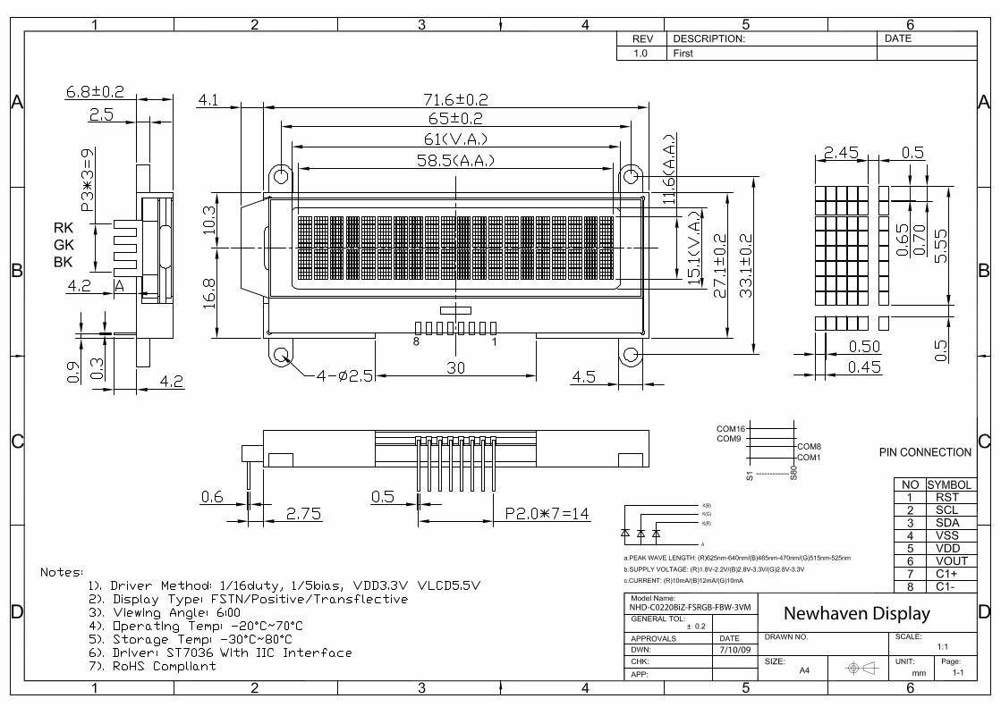
NHD-C0220BiZ-FSRGB-FBW-3VM Newhaven Display
7/10/09
RKGKBK
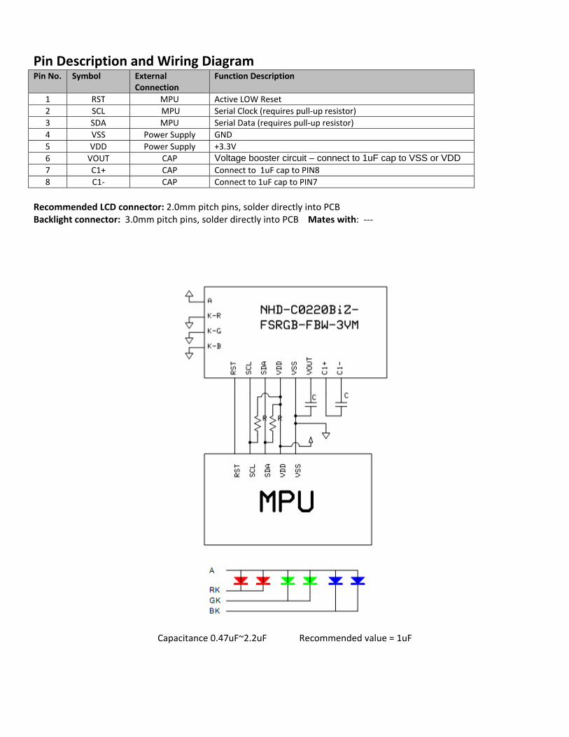
Pin Description and Wiring Diagram Pin No. Symbol External
Connection Function Description
1 RST MPU Active LOW Reset2 SCL MPU Serial Clock (requires pull‐up resistor)3 SDA MPU Serial Data (requires pull‐up resistor)4 VSS Power Supply GND5 VDD Power Supply +3.3V6 VOUT CAP Voltage booster circuit – connect to 1uF cap to VSS or VDD7 C1+ CAP Connect to 1uF cap to PIN88 C1‐ CAP Connect to 1uF cap to PIN7
Recommended LCD connector: 2.0mm pitch pins, solder directly into PCB Backlight connector: 3.0mm pitch pins, solder directly into PCB Mates with: ‐‐‐
Capacitance 0.47uF~2.2uF Recommended value = 1uF

Electrical Characteristics
Item Symbol Condition Min. Typ. Max. UnitOperating Temperature Range Top Absolute Max ‐20 ‐ +70 ⁰C Storage Temperature Range Tst Absolute Max ‐30 ‐ +80 ⁰C Supply Voltage VDD 2.7 3.3 3.5 V Supply Current IDD VDD=3.3V 1 mASupply for LCD (contrast) VDD‐V0 VLCD=VDD‐V0 2.7 7.0 V “H” Level input Vih 0.7VDD ‐ VDD V “L” Level input Vil 0 ‐ 0.8 V “H” Level output Voh 0.7VDD ‐ VDD V “L” Level output Vol ‐ ‐ 0.8 V Backlight Supply Voltage – RED VLED ‐ 2.2 V Backlight Supply Current – RED Iled ‐ 10 mABacklight Supply Voltage – GREEN VLED ‐ 3.3 V Backlight Supply Current – GREEN Iled ‐ 10 mABacklight Supply Voltage – BLUE VLED ‐ 3.3 V Backlight Supply Current – BLUE Iled ‐ 12 mA
Optical Characteristics Item Symbol Condition Min. Typ. Max. Unit
Viewing Angle ‐ Vertical AV Cr ≥ 2 ‐60 +35 ⁰ Viewing Angle ‐ Horizontal AH Cr ≥ 2 ‐40 +40 ⁰ Contrast Ratio Cr ‐ 6 ‐ Response Time (rise) Tr ‐ ‐ 150 200 msResponse Time (fall) Tf ‐ ‐ 150 200 ms
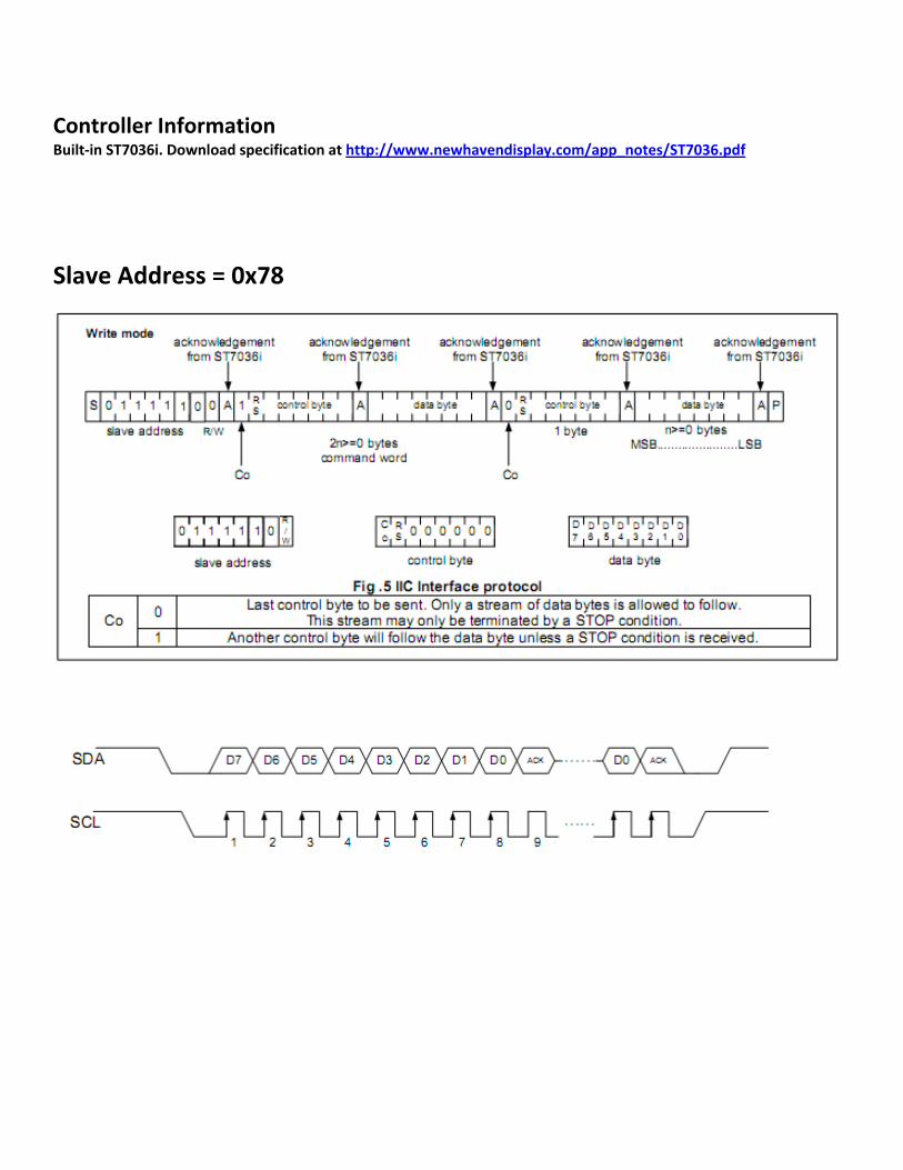
Controller Information Built‐in ST7036i. Download specification at http://www.newhavendisplay.com/app_notes/ST7036.pdf
Slave Address = 0x78
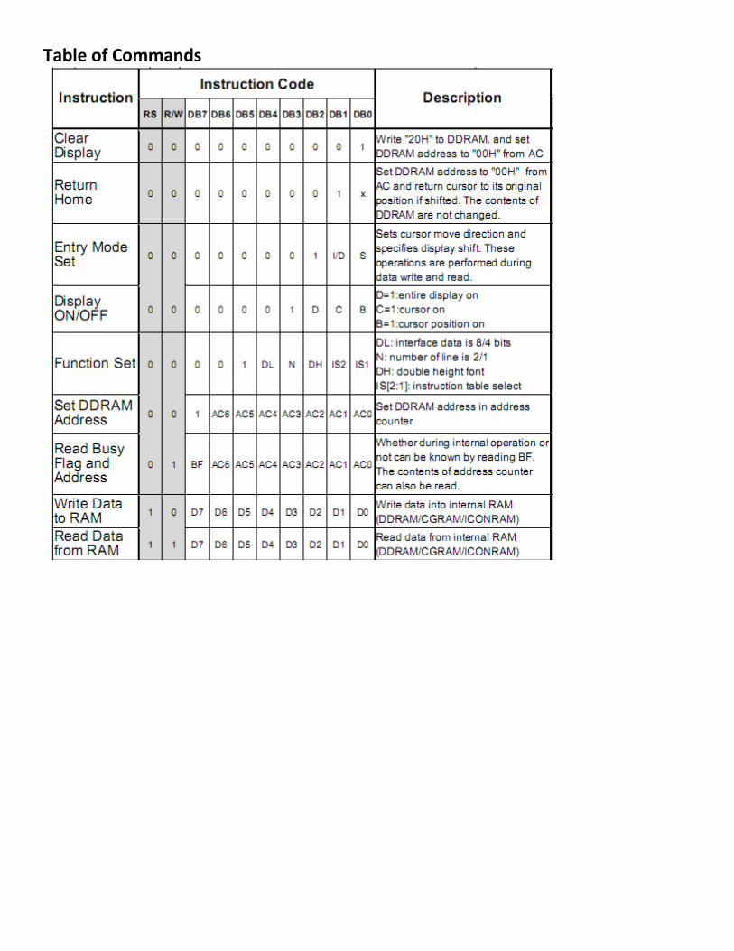
Table of Commands

Built‐in Font Table (OPR1 = 0, OPR2 = 0)

Example Initialization Program /**************************************************** * Initialization For ST7036i * *****************************************************/ void init_LCD() I2C_Start(); I2C_out(Slave);//Slave=0x78 I2C_out(Comsend);//Comsend = 0x00 I2C_out(0x38); delay(10); I2C_out(0x39); delay(10); I2C_out(0x14); I2C_out(0x78); I2C_out(0x5E); I2C_out(0x6D); I2C_out(0x0C); I2C_out(0x01); I2C_out(0x06); delay(10); I2C_Stop(); /*****************************************************/ /**************************************************** * Output command or data via I2C * *****************************************************/ void I2C_out(unsigned char j) //I2C Output int n; unsigned char d; d=j; for(n=0;n<8;n++) if((d&0x80)==0x80) SDA=1; else SDA=0; d=(d<<1); SCL = 0; SCL = 1; SCL = 0; SCL = 1; while(SDA==1) SCL=0; SCL=1; SCL=0; /*****************************************************/

/**************************************************** * I2C Start * *****************************************************/ void I2C_Start(void) SCL=1; SDA=1; SDA=0; SCL=0; /*****************************************************/ /**************************************************** * I2C Stop * *****************************************************/ void I2C_Stop(void) SDA=0; SCL=0; SCL=1; SDA=1; /*****************************************************/ /**************************************************** * Send string of ASCII data to LCD * *****************************************************/ void Show(unsigned char *text) int n,d; d=0x00; I2C_Start(); I2C_out(Slave); //Slave=0x78 I2C_out(Datasend);//Datasend=0x40 for(n=0;n<20;n++) I2C_out(*text); ++text; I2C_Stop(); /*****************************************************/ /*****************************************************/ /*****************************************************/

Quality Information
Test Item Content of Test Test Condition NoteHigh Temperature storage Endurance test applying the high
storage temperature for a long time. +80⁰C , 200hrs 2
Low Temperature storage Endurance test applying the low storage temperature for a long time.
‐30⁰C , 200hrs 1,2
High Temperature Operation
Endurance test applying the electric stress (voltage & current) and the high thermal stress for a long time.
+70⁰C 200hrs 2
Low Temperature Operation
Endurance test applying the electric stress (voltage & current) and the low thermal stress for a long time.
‐20⁰C , 200hrs 1,2
High Temperature / Humidity Operation
Endurance test applying the electric stress (voltage & current) and the high thermal with high humidity stress for a long time.
+60⁰C , 90% RH , 96hrs 1,2
Thermal Shock resistance Endurance test applying the electric stress (voltage & current) during a cycle of low and high thermal stress.
‐20⁰C,30min ‐> 25⁰C,5min ‐> 70⁰C,30min = 1 cycle 10 cycles
Vibration test Endurance test applying vibration to simulate transportation and use.
10‐55Hz , 15mm amplitude. 60 sec in each of 3 directions X,Y,Z For 15 minutes
3
Static electricity test Endurance test applying electric static discharge.
VS=800V, RS=1.5kΩ, CS=100pF One time
Note 1: No condensation to be observed. Note 2: Conducted after 4 hours of storage at 25⁰C, 0%RH. Note 3: Test performed on product itself, not inside a container.
Precautions for using LCDs/LCMs See Precautions at www.newhavendisplay.com/specs/precautions.pdf
Warranty Information and Terms & Conditions http://www.newhavendisplay.com/index.php?main_page=terms

ST
Sitronix ST7036 Dot Matrix LCD Controller/Driver
V1.7a 2007/10/17 1/70
Features 5 x 8 dot matrix possible Low power operation support:
-- 2.7 to 5.5V Range of LCD driver power
-- 3.0 to 7.0V 4-bit, 8-bit, serial or I 2C-bus MPU interface
enabled 80 x 8-bit display RAM (80 characters max.) 10,240-bit character generator ROM for a
total of 256 character fonts(max) 64 x 8-bit character generator RAM(max) Support two display mode:
16-com x 100-seg and 80 ICON 24-com x 80-seg and 80 ICON
16 x 5 –bit ICON RAM(max)
Wide range of instruction functions: Display clear, cursor home, display on/off, cursor on/off, display character blink, cursor shift, display shift, double height font
Automatic reset circuit that initializes the controller/driver after power on and external reset pin
Internal oscillator(Frequency=540kHz) and external clock
Built-in voltage booster and follower circuit (low power consumption )
COM/SEG direction selectable Multi-selectable for CGRAM/CGROM size Instruction compatible to ST7066U and
KS0066U and HD44780 Available in COG type
Description The ST7036 dot-matrix liquid crystal display controller can display alphanumeric, Japanese kana characters, and symbols. It can be configured to drive a dot-matrix liquid crystal display under the control of a 4 / 8-bit with 6800-series, serial or fast I2C interface microprocessor. Since all the functions such as display RAM, character generator ROM/RAM and liquid crystal driver, required for driving a dot-matrix liquid crystal display are internally provided on one chip, a minimal system can be used with this controller/driver. The ST7036 character generator ROM size is 256 5x8dot bits which can be used to generate 256 different character fonts (5x8dot).
The ST7036 is suitable for low voltage supply (2.7V to 5.5V) and is perfectly suitable for any portable product which is driven by the battery and requires low power consumption. The display resolution of ST7036 dot-matrix LCD driver can be either 1-line x 20 characters, 2-line x 20 characters or 3-line x 16 characters with 80 bit ICON. The ST7036 dot-matrix LCD driver does not need extra cascaded drivers.
product Name Character generat or
ROM Size OPR1 OPR2 Support Character
ST7036-0A 256 1 1 English / Japan/Europe - - - - -
ST7036 6800-4bit / 8bit,4-Line interface (without IIC interface)
ST7036i IIC interface

ST7036
V1.7a 2007/10/17 2/70
ST7036 Serial Specification Revision History
Version Date Description
0.1a 2003/04/28 1st Edition
0.1b 2003/06/03 PAD Dimension: IC L mark location modified Chip Size X/Y modified
0.2a 2003/09/01 1. Include ST7036i
1.0 2003/10/24 1. Add application circuit for 3 line display. 2. 4 bit interface program example modified.
1.1 2003/12/24 1. Remove the instruction of frequency adjust. 2. Add the detail of CGRAM/CGROM arrangement.
1.2 2004/5/13 Remove ‘Preliminary’.
1.3 2004/5/26 1. Correct the I/O pad configuration. 2. Add comments for I2C application.
1.4 2004/10/20 1. To modify icon RAM mapping. ( P.24 )
1.5 2005/06/13 Modify operating temperature range Ta=-35°C to 85°C
1.6 2005/10/17
1. To modify Operating Temperature Range Ta=-30°C to 85°C 2. To modify Storage Temperature Range Ta=-65°C to 150°C 3. To modify the vlcd voltage Range 3.0v~7.0v 4. To modify the limiting values -0.3v~+6.0v 5. To add Chip Thickness: 635 um
1.7 2006/7/10 1. To modify Chip Thickness: 480 um
1.7a 2007/10/17 1. Adding description of 4-line interface in cover

ST7036
V1.7a 2007/10/17 3/70
Pad Dimensions
Chip Size: 5190.0 X 910.0 µm Chip Thickness: 480 µm Bump Pitch : 55 µm ( min ) Bump Height : 17 µm ( typ. ) Bump Size :
Pad No.1~52 : 56 x 72 µm Pad No.53~170 : 35 x 101 µm

ST7036
V1.7a 2007/10/17 4/70
Pad Location Coordinates(N3=0 1 line/2 line) Pad No. Function X Y Pad No. Function X Y
1 XRESET 1859 393 41 CLS -1181 393
2 OSC 1783 393 42 CAP1N -1257 393
3 VDD 1707 393 43 CAP1N -1333 393
4 RS 1631 393 44 VOUT -1409 393
5 CSB 1555 393 45 VOUT -1485 393
6 RW 1479 393 46 V0 -1561 393
7 E 1403 393 47 V0 -1637 393
8 DB0 1327 393 48 V1 -1713 393
9 DB1 1251 393 49 V2 -1789 393
10 DB2 1175 393 50 V3 -1865 393
11 DB3 1099 393 51 V4 -1941 393
12 DB4 1023 393 52 NC -2017 393
13 DB5 947 393 53 COM[8] -2125 378
14 DB6 871 393 54 COM[7] -2180 378
15 DB7 795 393 55 COM[6] -2235 378
16 VSS 719 393 56 COM[5] -2290 378
17 VSS 643 393 57 COM[4] -2518 365
18 VSS 567 393 58 COM[3] -2518 310
19 OPF1 491 393 59 COM[2] -2518 255
20 OPF2 415 393 60 COM[1] -2518 200
21 OPR1 339 393 61 COMI1 -2518 145
22 OPR2 263 393 62 SEG[1] -2518 90
23 SHLC 187 393 63 SEG[2] -2518 35
24 SHLS 111 393 64 SEG[3] -2518 -20
25 N3 35 393 65 SEG[4] -2518 -75
26 TEST1 -41 393 66 SEG[5] -2518 -130
27 VDD -117 393 67 SEG[6] -2518 -185
28 VDD -193 393 68 SEG[7] -2518 -240
29 VDD -269 393 69 SEG[8] -2518 -295
30 VIN -345 393 70 SEG[9] -2518 -350
31 VIN -421 393 71 SEG[10] -2253 -378
32 VOUT -497 393 72 SEG[11] -2198 -378
33 VOUT -573 393 73 SEG[12] -2143 -378
34 PSB -649 393 74 SEG[13] -2088 -378
35 VSS -725 393 75 SEG[14] -2033 -378
36 PSI2B -801 393 76 SEG[15] -1978 -378
37 CAP1P -877 393 77 SEG[16] -1923 -378
38 CAP1P -953 393 78 SEG[17] -1868 -378
39 EXT -1029 393 79 SEG[18] -1813 -378
40 VSS -1105 393 80 SEG[19] -1758 -378

ST7036
V1.7a 2007/10/17 5/70
Pad No. Function X Y Pad No. Function X Y
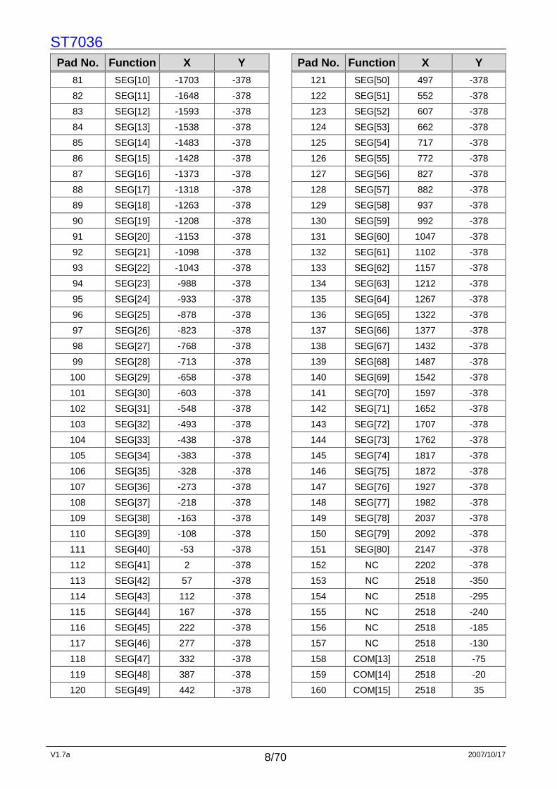
81 SEG[20] -1703 -378 121 SEG[60] 497 -378
82 SEG[21] -1648 -378 122 SEG[61] 552 -378
83 SEG[22] -1593 -378 123 SEG[62] 607 -378
84 SEG[23] -1538 -378 124 SEG[63] 662 -378
85 SEG[24] -1483 -378 125 SEG[64] 717 -378
86 SEG[25] -1428 -378 126 SEG[65] 772 -378
87 SEG[26] -1373 -378 127 SEG[66] 827 -378
88 SEG[27] -1318 -378 128 SEG[67] 882 -378
89 SEG[28] -1263 -378 129 SEG[68] 937 -378
90 SEG[29] -1208 -378 130 SEG[69] 992 -378
91 SEG[30] -1153 -378 131 SEG[70] 1047 -378
92 SEG[31] -1098 -378 132 SEG[71] 1102 -378
93 SEG[32] -1043 -378 133 SEG[72] 1157 -378
94 SEG[33] -988 -378 134 SEG[73] 1212 -378
95 SEG[34] -933 -378 135 SEG[74] 1267 -378
96 SEG[35] -878 -378 136 SEG[75] 1322 -378
97 SEG[36] -823 -378 137 SEG[76] 1377 -378
98 SEG[37] -768 -378 138 SEG[77] 1432 -378
99 SEG[38] -713 -378 139 SEG[78] 1487 -378
100 SEG[39] -658 -378 140 SEG[79] 1542 -378
101 SEG[40] -603 -378 141 SEG[80] 1597 -378
102 SEG[41] -548 -378 142 SEG[81] 1652 -378
103 SEG[42] -493 -378 143 SEG[82] 1707 -378
104 SEG[43] -438 -378 144 SEG[83] 1762 -378
105 SEG[44] -383 -378 145 SEG[84] 1817 -378
106 SEG[45] -328 -378 146 SEG[85] 1872 -378
107 SEG[46] -273 -378 147 SEG[86] 1927 -378
108 SEG[47] -218 -378 148 SEG[87] 1982 -378
109 SEG[48] -163 -378 149 SEG[88] 2037 -378
110 SEG[49] -108 -378 150 SEG[89] 2092 -378
111 SEG[50] -53 -378 151 SEG[90] 2147 -378
112 SEG[51] 2 -378 152 SEG[91] 2202 -378
113 SEG[52] 57 -378 153 SEG[92] 2518 -350
114 SEG[53] 112 -378 154 SEG[93] 2518 -295
115 SEG[54] 167 -378 155 SEG[94] 2518 -240
116 SEG[55] 222 -378 156 SEG[95] 2518 -185
117 SEG[56] 277 -378 157 SEG[96] 2518 -130
118 SEG[57] 332 -378 158 SEG[97] 2518 -75
119 SEG[58] 387 -378 159 SEG[98] 2518 -20
120 SEG[59] 442 -378 160 SEG[99] 2518 35
ST7036
V1.7a 2007/10/17 6/70
Pad No. Function X Y Pad No. Function X Y
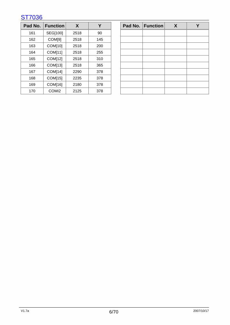
161 SEG[100] 2518 90
162 COM[9] 2518 145
163 COM[10] 2518 200
164 COM[11] 2518 255
165 COM[12] 2518 310
166 COM[13] 2518 365
167 COM[14] 2290 378
168 COM[15] 2235 378
169 COM[16] 2180 378
170 COMI2 2125 378

ST7036
V1.7a 2007/10/17 7/70
Pad Location Coordinates(N3=1 3 line) Pad No. Function X Y Pad No. Function X Y
1 XRESET 1859 393 41 CLS -1181 393
2 OSC 1783 393 42 CAP1N -1257 393
3 VDD 1707 393 43 CAP1N -1333 393
4 RS 1631 393 44 VOUT -1409 393
5 CSB 1555 393 45 VOUT -1485 393
6 RW 1479 393 46 V0 -1561 393
7 E 1403 393 47 V0 -1637 393
8 DB0 1327 393 48 V1 -1713 393
9 DB1 1251 393 49 V2 -1789 393
10 DB2 1175 393 50 V3 -1865 393
11 DB3 1099 393 51 V4 -1941 393
12 DB4 1023 393 52 NC -2017 393
13 DB5 947 393 53 COM[12] -2125 378
14 DB6 871 393 54 COM[11] -2180 378
15 DB7 795 393 55 COM[10] -2235 378
16 VSS 719 393 56 COM[9] -2290 378
17 VSS 643 393 57 COM[8] -2518 365
18 VSS 567 393 58 COM[7] -2518 310
19 OPF1 491 393 59 COM[6] -2518 255
20 OPF2 415 393 60 COM[5] -2518 200
21 OPR1 339 393 61 NC -2518 145
22 OPR2 263 393 62 COM[4] -2518 90
23 SHLC 187 393 63 COM[3] -2518 35
24 SHLS 111 393 64 COM[2] -2518 -20
25 N3 35 393 65 COM[1] -2518 -75
26 TEST1 -41 393 66 COMI1 -2518 -130
27 VDD -117 393 67 NC -2518 -185
28 VDD -193 393 68 NC -2518 -240
29 VDD -269 393 69 NC -2518 -295
30 VIN -345 393 70 NC -2518 -350
31 VIN -421 393 71 NC -2253 -378
32 VOUT -497 393 72 SEG[1] -2198 -378
33 VOUT -573 393 73 SEG[2] -2143 -378
34 PSB -649 393 74 SEG[3] -2088 -378
35 VSS -725 393 75 SEG[4] -2033 -378
36 PSI2B -801 393 76 SEG[5] -1978 -378
37 CAP1P -877 393 77 SEG[6] -1923 -378
38 CAP1P -953 393 78 SEG[7] -1868 -378
39 EXT -1029 393 79 SEG[8] -1813 -378
40 VSS -1105 393 80 SEG[9] -1758 -378
ST7036
V1.7a 2007/10/17 8/70
Pad No. Function X Y Pad No. Function X Y
81 SEG[10] -1703 -378 121 SEG[50] 497 -378
82 SEG[11] -1648 -378 122 SEG[51] 552 -378
83 SEG[12] -1593 -378 123 SEG[52] 607 -378
84 SEG[13] -1538 -378 124 SEG[53] 662 -378
85 SEG[14] -1483 -378 125 SEG[54] 717 -378
86 SEG[15] -1428 -378 126 SEG[55] 772 -378
87 SEG[16] -1373 -378 127 SEG[56] 827 -378
88 SEG[17] -1318 -378 128 SEG[57] 882 -378
89 SEG[18] -1263 -378 129 SEG[58] 937 -378
90 SEG[19] -1208 -378 130 SEG[59] 992 -378
91 SEG[20] -1153 -378 131 SEG[60] 1047 -378
92 SEG[21] -1098 -378 132 SEG[61] 1102 -378
93 SEG[22] -1043 -378 133 SEG[62] 1157 -378
94 SEG[23] -988 -378 134 SEG[63] 1212 -378
95 SEG[24] -933 -378 135 SEG[64] 1267 -378
96 SEG[25] -878 -378 136 SEG[65] 1322 -378
97 SEG[26] -823 -378 137 SEG[66] 1377 -378
98 SEG[27] -768 -378 138 SEG[67] 1432 -378
99 SEG[28] -713 -378 139 SEG[68] 1487 -378
100 SEG[29] -658 -378 140 SEG[69] 1542 -378
101 SEG[30] -603 -378 141 SEG[70] 1597 -378
102 SEG[31] -548 -378 142 SEG[71] 1652 -378
103 SEG[32] -493 -378 143 SEG[72] 1707 -378
104 SEG[33] -438 -378 144 SEG[73] 1762 -378
105 SEG[34] -383 -378 145 SEG[74] 1817 -378
106 SEG[35] -328 -378 146 SEG[75] 1872 -378
107 SEG[36] -273 -378 147 SEG[76] 1927 -378
108 SEG[37] -218 -378 148 SEG[77] 1982 -378
109 SEG[38] -163 -378 149 SEG[78] 2037 -378
110 SEG[39] -108 -378 150 SEG[79] 2092 -378
111 SEG[40] -53 -378 151 SEG[80] 2147 -378
112 SEG[41] 2 -378 152 NC 2202 -378
113 SEG[42] 57 -378 153 NC 2518 -350
114 SEG[43] 112 -378 154 NC 2518 -295
115 SEG[44] 167 -378 155 NC 2518 -240
116 SEG[45] 222 -378 156 NC 2518 -185
117 SEG[46] 277 -378 157 NC 2518 -130
118 SEG[47] 332 -378 158 COM[13] 2518 -75
119 SEG[48] 387 -378 159 COM[14] 2518 -20
120 SEG[49] 442 -378 160 COM[15] 2518 35

ST7036
V1.7a 2007/10/17 9/70
Pad No. Function X Y Pad No. Function X Y
161 COM[16] 2518 90
162 COM[17] 2518 145
163 COM[18] 2518 200
164 COM[19] 2518 255
165 COM[20] 2518 310
166 COM[21] 2518 365
167 COM[22] 2290 378
168 COM[23] 2235 378
169 COM[24] 2180 378
170 COMI2 2125 378
ST7036
V1.7a 2007/10/17 10/70
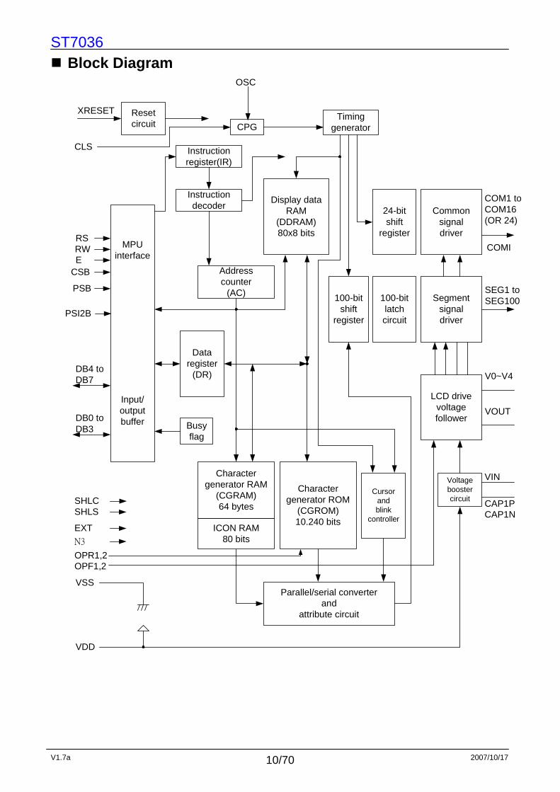
Block Diagram
RW
Resetcircuit CPG
Timinggenerator
Instructionregister(IR)
Instructiondecoder
Display dataRAM
(DDRAM)80x8 bits
24-bitshift
register
Commonsignaldriver
100-bitlatchcircuit
100-bitshift
register
Segmentsignaldriver
LCD drivevoltagefollower
Addresscounter
(AC)
Dataregister
(DR)
Busyflag
MPUinterface
Input/outputbuffer
Charactergenerator RAM
(CGRAM)64 bytes
Charactergenerator ROM
(CGROM)10.240 bits
Cursorandblink
controller
Parallel/serial converterand
attribute circuit
RS
E
DB4 toDB7
DB0 toDB3
VDD
OSC
COM1 toCOM16(OR 24)
SEG1 toSEG100
XRESET
VSS
OPF1,2
SHLC
EXT
OPR1,2
Voltageboostercircuit
COMI
CLS
SHLS
V0~V4
VOUT
PSB
CAP1PCAP1N
VIN
ICON RAM80 bits
CSB
N3
PSI2B
ST7036
V1.7a 2007/10/17 11/70
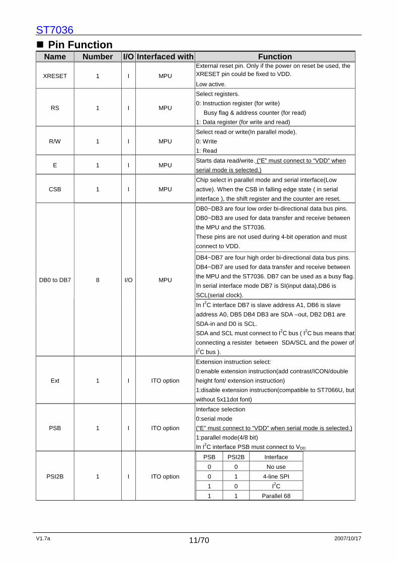
Pin Function Name Number I/O Interfaced with Function
XRESET 1 I MPU
External reset pin. Only if the power on reset be used, the XRESET pin could be fixed to VDD.
Low active.
RS 1 I MPU
Select registers.
0: Instruction register (for write)
Busy flag & address counter (for read)
1: Data register (for write and read)
R/W 1 I MPU
Select read or write(In parallel mode).
0: Write
1: Read
E 1 I MPU Starts data read/write. (“E” must connect to “VDD” when
serial mode is selected.)
CSB 1 I MPU
Chip select in parallel mode and serial interface(Low
active). When the CSB in falling edge state ( in serial
interface ), the shift register and the counter are reset.
DB0~DB3 are four low order bi-directional data bus pins.
DB0~DB3 are used for data transfer and receive between
the MPU and the ST7036.
These pins are not used during 4-bit operation and must
connect to VDD.
DB4~DB7 are four high order bi-directional data bus pins.
DB4~DB7 are used for data transfer and receive between
the MPU and the ST7036. DB7 can be used as a busy flag.
In serial interface mode DB7 is SI(input data),DB6 is
SCL(serial clock).
DB0 to DB7 8 I/O MPU
In I2C interface DB7 is slave address A1, DB6 is slave
address A0, DB5 DB4 DB3 are SDA –out, DB2 DB1 are
SDA-in and D0 is SCL.
SDA and SCL must connect to I2C bus ( I2C bus means that
connecting a resister between SDA/SCL and the power of
I2C bus ).
Ext 1 I ITO option
Extension instruction select:
0:enable extension instruction(add contrast/ICON/double
height font/ extension instruction)
1:disable extension instruction(compatible to ST7066U, but
without 5x11dot font)
PSB 1 I ITO option
Interface selection
0:serial mode
(“E” must connect to “VDD” when serial mode is selected.)
1:parallel mode(4/8 bit)
In I2C interface PSB must connect to VDD
PSI2B 1 I ITO option
PSB PSI2B Interface
0 0 No use
0 1 4-line SPI
1 0 I2C
1 1 Parallel 68

ST7036
V1.7a 2007/10/17 12/70
Name Number I/O Interfaced with Function
OPR1,OPR2 2 I ITO option
Character generator select:
OPR1 OPR2 CGROM CGRAM
0 0 240 8
0 1 250 6
1 0 248 8
1 1 256 0
SHLC 1 I ITO option
Common signals direction select:
0:Com1~24←Row address 23~0(Invert)
1:Com1~24←Row address 0~23(Normal)
SHLS 1 I ITO option
Segment signals direction select:
0:Seg1~100←Column address 99~0(Invert)
1:Seg1~100←Column address 0~99(Normal)
COM1 to
COM16 16 O LCD
Common signals that are not used are changed
to non-selection waveform. COM9 to COM16
are non-selection waveforms at 1/8 or 1/9 duty factor
COMI2
COMI1 1 O LCD
ICON common signals
Seg1~Seg10
Seg91~Seg100 21 O LCD
Select “N3” pin for common or segment waveform output
(follow up table 2 defined)
N3 1 I ITO option
1 line/2 line or 3 line select :
0:1 line/2 line SEG0~SEG100:normal
1:3 line COMI1,SEG1~SEG5,SEG97~SEG100 re-defined
SEG11 to
SEG90 80 O LCD Segment signals
The built-in voltage follower circuit selection
OPF1 OPF2 Bias select
0 0 Built-in voltage follower(only use at EXT=0)
0 1 Built-in bias resistor(3.3KΩ)
1 0 Built-in bias resistor(9.6KΩ)
OPF1,OPF2 2 I ITO option
1 1 External bias resistor select
CAP1P 2 - Power supply
CAP1N 2 - Power supply
For voltage booster circuit(VDD-VSS)
External capacitor about 0.1u~4.7uf
VIN 2 - Power supply Input the voltage to booster
VOUT 4 - Power supply DC/DC voltage converter. Connect a capacitor between this
terminal and VIN when the built-in booster is used.
V0 to V4 6 - Power supply
Power supply for LCD drive
V0-Vss = 7V (Max)
Built-in/external Voltage follower circuit
VDD,VSS 4,5 - Power supply VDD : 2.7V to 5.5V, VSS: 0V
CLS 1 I ITO option
Internal/External oscillation select
0:external clock
1:internal oscillation
OSC 1 I Oscillation
When the pin input is an external clock, it must be input to
OSC.
When the on-chip oscillator is used, it must be connected
to VDD.
TEST1 1 I/O Test pin TEST1 must connect to VDD.

ST7036
V1.7a 2007/10/17 13/70
EXT option pin difference table Mode
Difference
Normal mode (EXT=1) ( Instruction compatible to ST7066U )
Extension mode (EXT=0)
Booster Always OFF ON/OFF controlled by instruction
Bias (V0~V4)
Can’t use the follower circuit
Only use external resistor or internal resistor(1/5
bias)
Follower or internal/external resistor selectable
Contrast adjust Control by external VR
1. Controlled by instruction with follower
2. Controlled by external VR with
internal/external resistor
ICON RAM Can’t be use RAM size has 80 bit width(S1~S80).
Instruction Control normal instruction similar to ST7066U. Control extension instruction for low power
consumption.
Double height font Only 5x8 font Can set 5x8 or 5x16 font
ST7036
V1.7a 2007/10/17 14/70
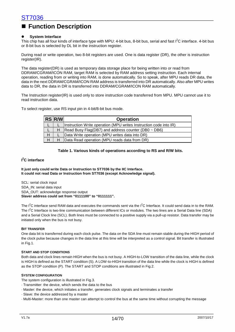
Function Description System Interface This chip has all four kinds of interface type with MPU: 4-bit bus, 8-bit bus, serial and fast I2C interface. 4-bit bus or 8-bit bus is selected by DL bit in the instruction register. During read or write operation, two 8-bit registers are used. One is data register (DR), the other is instruction register(IR). The data register(DR) is used as temporary data storage place for being written into or read from DDRAM/CGRAM/ICON RAM, target RAM is selected by RAM address setting instruction. Each internal operation, reading from or writing into RAM, is done automatically. So to speak, after MPU reads DR data, the data in the next DDRAM/CGRAM/ICON RAM address is transferred into DR automatically. Also after MPU writes data to DR, the data in DR is transferred into DDRAM/CGRAM/ICON RAM automatically. The Instruction register(IR) is used only to store instruction code transferred from MPU. MPU cannot use it to read instruction data. To select register, use RS input pin in 4-bit/8-bit bus mode.
Table 1. Various kinds of operations according to R S and R/W bits.
I2C interface It just only could write Data or Instruction to ST70 36 by the IIC Interface. It could not read Data or Instruction from ST7036 (e xcept Acknowledge signal). SCL: serial clock input SDA_IN: serial data input SDA_OUT: acknowledge response output Slaver address could set from “0111100” to “0111111” . The I2C interface send RAM data and executes the commands sent via the I2C Interface. It could send data in to the RAM. The I2C Interface is two-line communication between different ICs or modules. The two lines are a Serial Data line (SDA) and a Serial Clock line (SCL). Both lines must be connected to a positive supply via a pull-up resistor. Data transfer may be initiated only when the bus is not busy. BIT TRANSFER One data bit is transferred during each clock pulse. The data on the SDA line must remain stable during the HIGH period of the clock pulse because changes in the data line at this time will be interpreted as a control signal. Bit transfer is illustrated in Fig.1. START AND STOP CONDITIONS Both data and clock lines remain HIGH when the bus is not busy. A HIGH-to-LOW transition of the data line, while the clock is HIGH is defined as the START condition (S). A LOW-to-HIGH transition of the data line while the clock is HIGH is defined as the STOP condition (P). The START and STOP conditions are illustrated in Fig.2. SYSTEM CONFIGURATION The system configuration is illustrated in Fig.3. · Transmitter: the device, which sends the data to the bus · Master: the device, which initiates a transfer, generates clock signals and terminates a transfer · Slave: the device addressed by a master · Multi-Master: more than one master can attempt to control the bus at the same time without corrupting the message
RS R/W Operation L L Instruction Write operation (MPU writes Instruction code into IR) L H Read Busy Flag(DB7) and address counter (DB0 ~ DB6) H L Data Write operation (MPU writes data into DR) H H Data Read operation (MPU reads data from DR)

ST7036
V1.7a 2007/10/17 15/70
· Arbitration: procedure to ensure that, if more than one master simultaneously tries to control the bus, only one is allowed to do so and the message is not corrupted
· Synchronization: procedure to synchronize the clock signals of two or more devices. ACKNOWLEDGE Acknowledge signal (ACK) is not BF signal in parall el interface. Each byte of eight bits is followed by an acknowledge bit. The acknowledge bit is a HIGH signal put on the bus by the transmitter during which time the master generates an extra acknowledge related clock pulse. A slave receiver which is addressed must generate an acknowledge after the reception of each byte. A master receiver must also generate an acknowledge after the reception of each byte that has been clocked out of the slave transmitter. The device that acknowledges must pull-down the SDA line during the acknowledge clock pulse, so that the SDA line is stable LOW during the HIGH period of the acknowledge related clock pulse (set-up and hold times must be taken into consideration). A master receiver must signal an end-of-data to the transmitter by not generating an acknowledge on the last byte that has been clocked out of the slave. In this event the transmitter must leave the data line HIGH to enable the master to generate a STOP condition. Acknowledgement on the I2C Interface is illustrated in Fig.4.
SDA
SCL
data linestable;
data valid
changeof dataallowed
Fig .1 Bit transfer
SDA
SCL
S P
START condition STOP condition Fig .2 Definition of START and STOP conditions
MASTERTRANSMITTER/
RECEIVER
SLAVERECEIVER (1)
0111100
SLAVERECEIVER (2)
0111101
SLAVERECEIVER (3)
0111110
SLAVERECEIVER (4)
0111111
SDASCL
Fig .3 System configuration
ST7036
V1.7a 2007/10/17 16/70
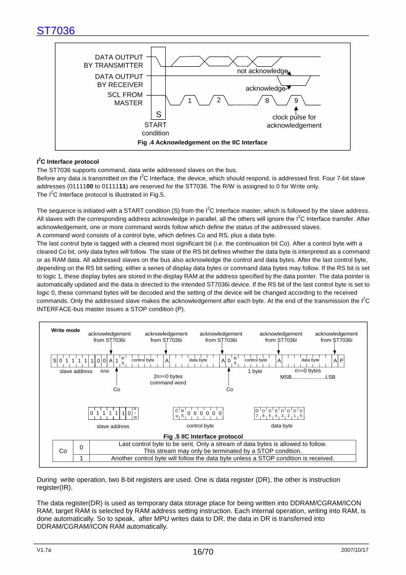
I2C Interface protocol The ST7036 supports command, data write addressed slaves on the bus. Before any data is transmitted on the I2C Interface, the device, which should respond, is addressed first. Four 7-bit slave addresses (0111100 to 0111111) are reserved for the ST7036. The R/W is assigned to 0 for Write only. The I2C Interface protocol is illustrated in Fig.5. The sequence is initiated with a START condition (S) from the I2C Interface master, which is followed by the slave address. All slaves with the corresponding address acknowledge in parallel, all the others will ignore the I2C Interface transfer. After acknowledgement, one or more command words follow which define the status of the addressed slaves. A command word consists of a control byte, which defines Co and RS, plus a data byte. The last control byte is tagged with a cleared most significant bit (i.e. the continuation bit Co). After a control byte with a cleared Co bit, only data bytes will follow. The state of the RS bit defines whether the data byte is interpreted as a command or as RAM data. All addressed slaves on the bus also acknowledge the control and data bytes. After the last control byte, depending on the RS bit setting; either a series of display data bytes or command data bytes may follow. If the RS bit is set to logic 1, these display bytes are stored in the display RAM at the address specified by the data pointer. The data pointer is automatically updated and the data is directed to the intended ST7036i device. If the RS bit of the last control byte is set to logic 0, these command bytes will be decoded and the setting of the device will be changed according to the received commands. Only the addressed slave makes the acknowledgement after each byte. At the end of the transmission the I2C INTERFACE-bus master issues a STOP condition (P).
During write operation, two 8-bit registers are used. One is data register (DR), the other is instruction register(IR). The data register(DR) is used as temporary data storage place for being written into DDRAM/CGRAM/ICON RAM, target RAM is selected by RAM address setting instruction. Each internal operation, writing into RAM, is done automatically. So to speak, after MPU writes data to DR, the data in DR is transferred into DDRAM/CGRAM/ICON RAM automatically.
1 2 8 9
S
DATA OUTPUTBY TRANSMITTER
DATA OUTPUTBY RECEIVER
SCL FROMMASTER
STARTcondition
not acknowledge
acknowledge
clock pulse foracknowledgement
Fig .4 Acknowledgement on the IIC Interface
S 0 1 1 1 1 1 RS0 A control byte A data byte
Co
0 RSA control byte A data byte A P
Co
slave address
acknowledgementfrom ST7036i
acknowledgementfrom ST7036i
acknowledgementfrom ST7036i
acknowledgementfrom ST7036i
acknowledgementfrom ST7036i
2n>=0 bytescommand word
n>=0 bytesMSB.......................LSB
1 byteR/W
Write mode
Co
RS 0 0 0 0 0 0
control byte
D7
D6
D5
D4
D3
D2
D1
D0
data byte
1 0
00 1 1 1 1R/W
1 0
slave address
Fig .5 IIC Interface protocol
0 Last control byte to be sent. Only a stream of data bytes is allowed to follow. This stream may only be terminated by a STOP condition. Co
1 Another control byte will follow the data byte unless a STOP condition is received.

ST7036
V1.7a 2007/10/17 17/70
The Instruction register(IR) is used only to store instruction code transferred from MPU. MPU cannot use it to read instruction data. To select register, use RS bit input in IIC interface.
Table 2. Various kinds of operations according to R S and R/W bits. Busy Flag (BF) When BF = "High”, it indicates that the internal operation is being processed. So during this time the next instruction cannot be accepted. BF can be read, when RS = Low and R/W = High (Read Instruction Operation), through DB7 port. Before executing the next instruction, be sure that BF is not High. Address Counter (AC) Address Counter(AC) stores DDRAM/CGRAM/ICON RAM address, transferred from IR. After writing into (reading from) DDRAM/CGRAM/ICON RAM, AC is automatically increased (decreased) by 1. When RS = "Low" and R/W = "High", AC can be read through DB0 ~ DB6 ports. Display Data RAM (DDRAM) Display data RAM (DDRAM) stores display data represented in 8-bit character codes. Its extended capacity is 80 x 8 bits, or 80 characters. The area in display data RAM (DDRAM) that is not used for display can be used as general data RAM. See Figure 6 for the relationships between DDRAM addresses and positions on the liquid crystal display. The DDRAM address (ADD ) is set in the address counter (AC) as hexadecimal. 1-line display (N3=0,N = 0) (Figure 7)
When there are fewer than 80 display characters, the display begins at the head position. For example, if using only the ST7036, 20 characters are displayed. See Figure 7. When the display shift operation is performed, the DDRAM address shifts. See Figure 8.
RS R/W Operation L L Instruction Write operation (MPU writes Instruction code into IR) H L Data Write operation (MPU writes data into DR)
ST7036
V1.7a 2007/10/17 18/70
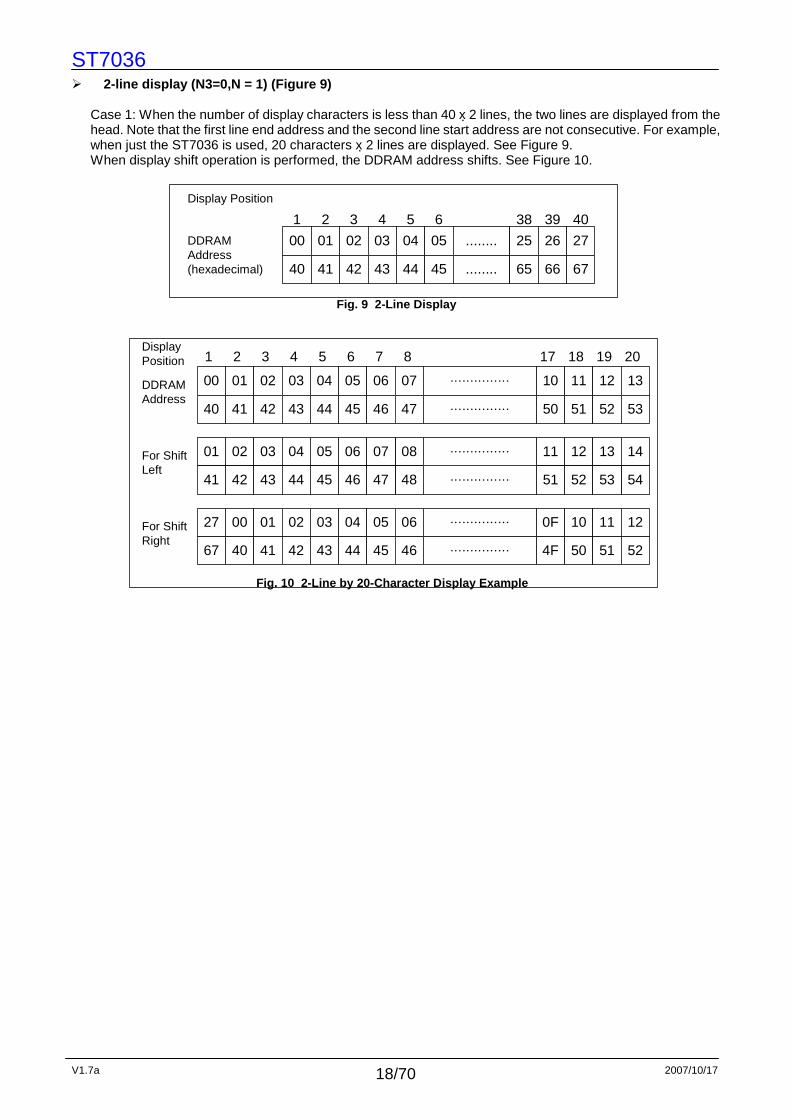
2-line display (N3=0,N = 1) (Figure 9) Case 1: When the number of display characters is less than 40 x 2 lines, the two lines are displayed from the head. Note that the first line end address and the second line start address are not consecutive. For example, when just the ST7036 is used, 20 characters x 2 lines are displayed. See Figure 9. When display shift operation is performed, the DDRAM address shifts. See Figure 10.
Fig. 9 2-Line Display
00 01 02 03 04 05 ........ 25 26 27DDRAMAddress(hexadecimal)
1 2 3 4 5 6 38 39 40
Display Position
40 41 42 43 44 45 ........ 65 66 67
DisplayPosition
Fig. 10 2-Line by 20-Character Display Example
DDRAMAddress
For ShiftLeft
For ShiftRight
1 2 3 4 5 6 7 8 17 18 19 20
00 01 02 03 04 05 0627
40 41 42 43 44 45 4667
0F 10 11 12
4F 50 51 52
00 01 02 03 04 05 06 07
0801 02 03 04 05 06 07
40 41 42 43 44 45 46 47
4841 42 43 44 45 46 47
10 11 12 13
50 51 52 53
11 12 13 14
5451 52 53
……………
……………
……………
……………
……………
……………

ST7036
V1.7a 2007/10/17 19/70
3-line display (N3=1,N =1) (Figure 11)
Case 1: When the number of display characters is less than 16 x 3 lines, the tree lines are displayed from the head. For example, when just the ST7036 is used, 16 characters x 3 lines are displayed. See Figure 11. When display shift operation is performed, the DDRAM address shifts. See Figure 12.
Fig. 12 3-Line Display
00 01 02 03 04 05 ........ 0D 0E 0FDDRAMAddress(hexadecimal)
1 2 3 4 5 6 14 15 16
Display Position
10 11 12 13 14 15 ........ 1D 1E 1F
20 21 22 23 24 25 ........ 2D 2E 2F
1 2 3 4 5 6 14 15 16
For Shift Left
For Shift Right
01 02 03 04 05 06 ........ 0E 0F 00
11 12 13 14 15 16 ........ 1E 1F 10
21 22 23 24 25 26 ........ 2E 2F 20
0F 00 01 02 03 04 ........ 0C 0D 0E
1 2 3 4 5 6 14 15 16
1F 10 11 12 13 14 ........ 1C 1D 1E
2F 20 21 22 23 24 ........ 2C 2D 2E
Fig. 11 3-Line Display
00 01 02 03 04 05 ........ 0D 0E 0FDDRAMAddress(hexadecimal)
1 2 3 4 5 6 14 15 16
Display Position
10 11 12 13 14 15 ........ 1D 1E 1F
20 21 22 23 24 25 ........ 2D 2E 2F

ST7036
V1.7a 2007/10/17 20/70
Character Generator ROM (CGROM) The character generator ROM generates 5 x 8 dot character patterns from 8-bit character codes. It can generate 240/250/248/256 5 x 8 dot character patterns(select by OPR1/2 ITO pin). User-defined character patterns are also available by mask-programmed ROM. Character Generator RAM (CGRAM) In the character generator RAM, the user can rewrite character patterns by program. For 5 x 8 dots, eight character patterns can be written. Write into DDRAM the character codes at the addresses shown as the left column of Table 5 to show the character patterns stored in CGRAM. See Table 5 for the relationship between CGRAM addresses and data and display patterns. Areas that are not used for display can be used as general data RAM. ICON RAM In the ICON RAM, the user can rewrite icon pattern by program. There are totally 80 dots for icon can be written. See Table 6 for the relationship between ICON RAM a ddress and data and the display patterns. Timing Generation Circuit The timing generation circuit generates timing signals for the operation of internal circuits such as DDRAM, CGROM and CGRAM. RAM read timing for display and internal operation timing by MPU access are generated separately to avoid interfering with each other. Therefore, when writing data to DDRAM, for example, there will be no undesirable interference, such as flickering, in areas other than the display area. LCD Driver Circuit(N3=0) LCD Driver circuit has 17 common and 100 segment signals for LCD driving. Data from CGRAM/CGROM/ICON is transferred to 100 bit segment latch serially, and then it is stored to 100 bit shift latch. When each common is selected by 17 bit common register, segment data also output through segment driver from 100 bit segment latch. In case of 1-line display mode, COM1 ~ COM8(with COMI) have 1/9 duty, and in 2-line mode, COM1 ~ COM16(with COMI) have 1/17 duty ratio. LCD Driver Circuit(N3=1) LCD Driver circuit has 25 common and 80 segment signals for LCD driving. Data from CGRAM/CGROM/ICON is transferred to 80 bit segment latch serially, and then it is stored to 80 bit shift latch. When each common is selected by 25 bit common register, segment data also output through segment driver from 80 bit segment latch. In case of 3-line display mode, COM1 ~ COM24(with COMI) have 1/25 duty. COM/SEG Output pins
N3 COMI1 COM [1:8]
SEG [1:5]
SEG [6:10]
SEG [11:90]
SEG [91:96]
SEG [97:100]
COM [9:16] COMI2
VSS COMI1 COM [1:8]
SEG [1:5]
SEG [6:10]
SEG [11:90]
SEG [91:96]
SEG [97:100]
COM [9:16] COMI2
VDD NC COM [5:12]
COM[4:1] + COMI1 NC SEG
[1:80] NC COM [13:16]
COM [17:24] COMI2
Table 3. COM/SEG output define Cursor/Blink Control Circuit It can generate the cursor or blink in the cursor/blink control circuit. The cursor or the blink appears in the digit at the display data RAM address set in the address counter.

ST7036
V1.7a 2007/10/17 21/70
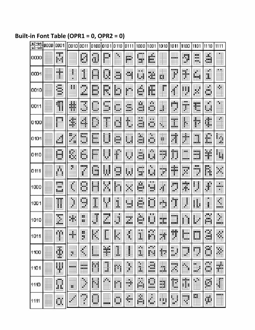
Table 4 Correspondence between Character Codes and Character Patterns
ST7036
V1.7a 2007/10/17 22/70
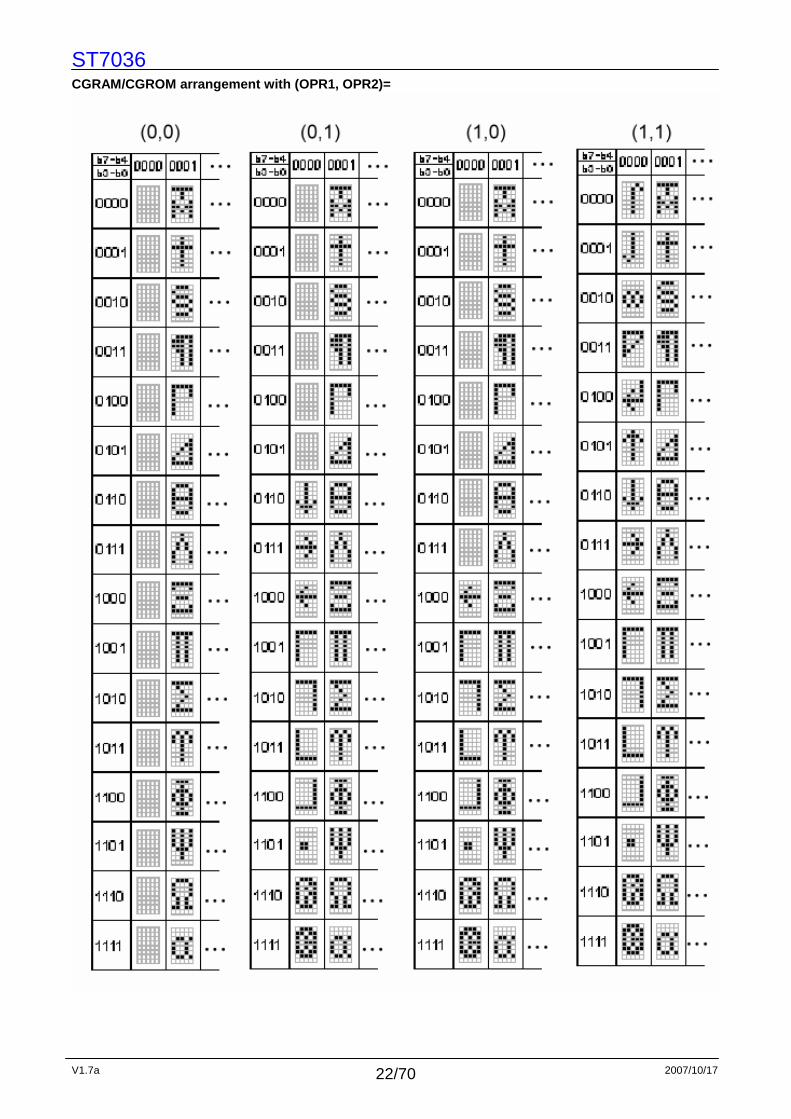
CGRAM/CGROM arrangement with (OPR1, OPR2)=

ST7036
V1.7a 2007/10/17 23/70
Character Code (DDRAM Data)
CGRAM Address
Character Patterns (CGRAM Data)
b7 b6 b5 b4 b3 b2 b1 b0 b5 b4 b3 b2 b1 b0 b7 b6 b5 b4 b3 b2 b1 b0 0 0 0 0 0 0 1 1 1 1 1 0 0 0 0 0 1 0 0 1 0 0 0 0 0 0 1 0 0 0 1 0 0 0 0 0 0 1 1 0 0 1 0 0 0 0 0 1 0 0 0 0 1 0 0 0 0 0 1 0 1 0 0 1 0 0 0 0 0 1 1 0 0 0 1 0 0
0 0 0 0 -
0 0 0
0 0 0
1 1 1
- - -
0 0 0 0 0 0 0 1 0 0 0 1 1 1 1 0 0 0 1 0 0 1 1 0 0 0 1 0 0 1 0 1 0 1 0 0 0 1 0 0 1 0 1 1 1 1 1 1 0 0 0 1 1 0 0 1 0 1 0 0 0 0 1 1 0 1 1 0 0 1 0 0 0 1 1 1 0 1 0 0 0 1
0 0 0 0 -
0 0 1
0 0 1
1 1 1
- - -
0 0 0 0 0
Table 5 Relationship between CGRAM Addresses, Char acter Codes (DDRAM) and Character patterns (CGRAM Data)
Notes: 1. Character code bits 0 to 2 correspond to CGRAM address bits 3 to 5 (3 bits: 8 types). 2. CGRAM address bits 0 to 2 designate the character pattern line position. The 8th line is the cursor position
and its display is formed by a logical OR with the cursor. Maintain the 8th line data, corresponding to the cursor display position, at 0 as the cursor display. If the 8th line data is 1, 1 bits will light up the 8th line regardless of the cursor presence.
3. Character pattern row positions correspond to CGRAM data bits 0 to 4 (bit 4 being at the left). 4. As shown Table 5, CGRAM character patterns are selected when character code bits 4 to 7 are all 0.
However, since character code bit 3 has no effect, the T display example above can be selected by either character code 00H or 08H.
5. “1” for CGRAM data corresponds to display selection and “0” to non-selection,“-“ Indicates no effect. 6. Different OPR1/2 ITO option can select different CGRAM size.

ST7036
V1.7a 2007/10/17 24/70
When ICON RAM data is filled the corresponding posi tion displayed is described as the following table.
When SHLS=1, ICON RAM map refer below table
ICON RAM bits
D7~D5 D4 D3 D2 D1 D0 ICON Address
N3 = 0 N3 = 1 N3 = 0 N3 = 1 N3 = 0 N3 = 1 N3 = 0 N3 = 1 N3 = 0 N3 = 1
00H - S1/S81 S1 S2/S82 S2 S3/S83 S3 S4/S84 S4 S5/S85 S5
01H - S6/S86 S6 S7/S87 S7 S8/S88 S8 S9/S89 S9 S10/S90 S10
02H - S11/S91 S11 S12/S92 S12 S13/S93 S13 S14/S94 S14 S15/S95 S15
03H - S16/S96 S16 S17/S97 S17 S18/S98 S18 S19/S99 S19 S20/S100 S20
04H - S21 S21 S22 S22 S23 S23 S24 S24 S25 S25
05H - S26 S26 S27 S27 S28 S28 S29 S29 S30 S30
06H - S31 S31 S32 S32 S33 S33 S34 S34 S35 S35
07H - S36 S36 S37 S37 S38 S38 S39 S39 S40 S40
08H - S41 S41 S42 S42 S43 S43 S44 S44 S45 S45
09H - S46 S46 S47 S47 S48 S48 S49 S49 S50 S50
0AH - S51 S51 S52 S52 S53 S53 S54 S54 S55 S55
0BH - S56 S56 S57 S57 S58 S58 S59 S59 S60 S60
0CH - S61 S61 S62 S62 S63 S63 S64 S64 S65 S65
0DH - S66 S66 S67 S67 S68 S68 S69 S69 S70 S70
0EH - S71 S71 S72 S72 S73 S73 S74 S74 S75 S75
0FH - S76 S76 S77 S77 S78 S78 S79 S79 S80 S80
When SHLS=0, ICON RAM map refer below table
ICON RAM bits
D7~D5 D4 D3 D2 D1 D0 ICON Address
N3 = 0 N3 = 1 N3 = 0 N3 = 1 N3 = 0 N3 = 1 N3 = 0 N3 = 1 N3 = 0 N3 = 1
00H - S100/S20 S80 S99/S19 S79 S98/S18 S78 S97/S17 S77 S96/S16 S76
01H - S95/S15 S75 S94/S14 S74 S93/S13 S73 S92S12 S72 S91/S11 S71
02H - S90/S10 S70 S89/S9 S69 S88/S8 S68 S87/S7 S67 S86/S6 S66
03H - S85/S5 S65 S84/S4 S64 S83/S3 S63 S82/S2 S62 S81/S1 S61
04H - S80 S60 S79 S59 S78 S58 S77 S57 S76 S56
05H - S75 S55 S74 S54 S73 S53 S72 S52 S71 S51
06H - S70 S50 S69 S49 S68 S48 S67 S47 S66 S46
07H - S65 S45 S64 S44 S63 S43 S62 S42 S61 S41
08H - S60 S40 S59 S39 S58 S38 S57 S37 S56 S36
09H - S55 S35 S54 S34 S53 S33 S52 S32 S51 S31
0AH - S50 S30 S49 S29 S48 S28 S47 S27 S46 S26
0BH - S45 S25 S44 S24 S43 S23 S42 S22 S41 S21
0CH - S40 S20 S39 S19 S38 S18 S37 S17 S36 S16
0DH - S35 S15 S34 S14 S33 S13 S32 S12 S31 S11
0EH - S30 S10 S29 S9 S28 S8 S27 S7 S26 S6
0FH - S25 S5 S24 S4 S23 S3 S22 S2 S21 S1
Table 6 ICON RAM map
ST7036
V1.7a 2007/10/17 25/70
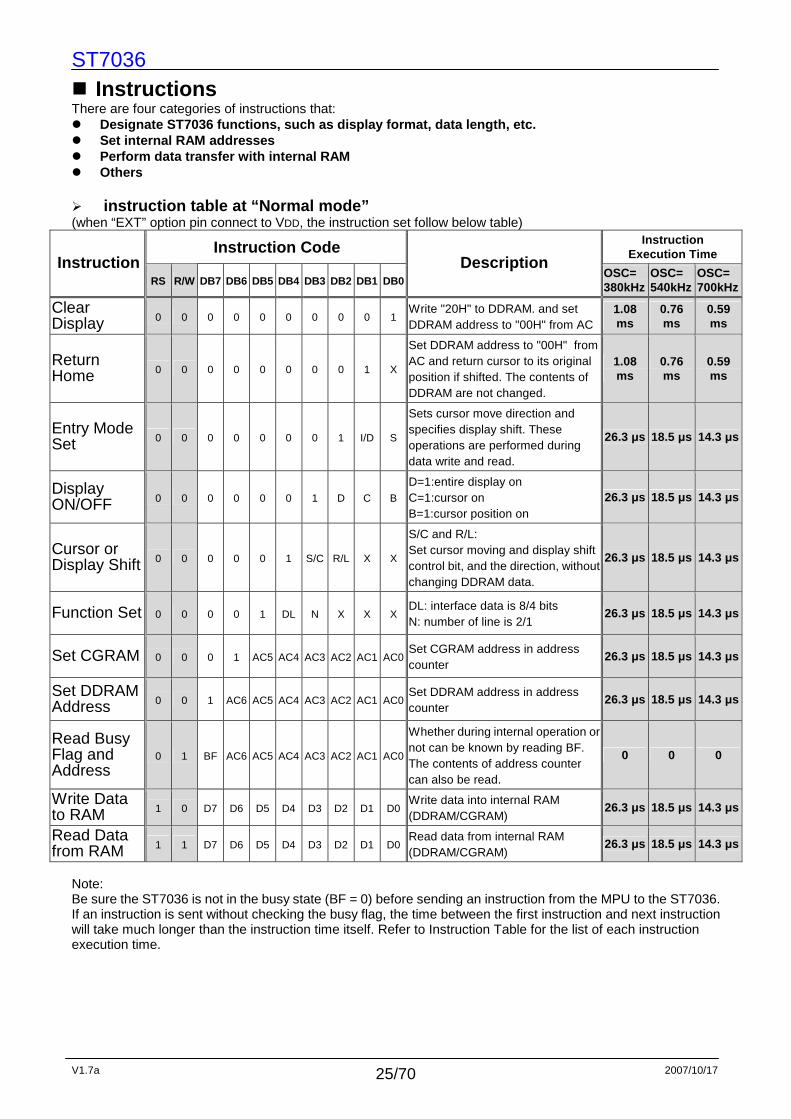
Instructions There are four categories of instructions that: Designate ST7036 functions, such as display format, data length, etc. Set internal RAM addresses Perform data transfer with internal RAM Others instruction table at “Normal mode” (when “EXT” option pin connect to VDD, the instruction set follow below table)
Instruction Code Instruction Execution Time
Instruction RS R/W DB7 DB6 DB5 DB4 DB3 DB2 DB1 DB0
Description OSC= 380kHz
OSC= 540kHz
OSC= 700kHz
Clear Display 0 0 0 0 0 0 0 0 0 1
Write "20H" to DDRAM. and set DDRAM address to "00H" from AC
1.08 ms
0.76 ms
0.59 ms
Return Home 0 0 0 0 0 0 0 0 1 X
Set DDRAM address to "00H" from AC and return cursor to its original position if shifted. The contents of DDRAM are not changed.
1.08 ms
0.76 ms
0.59 ms
Entry Mode Set 0 0 0 0 0 0 0 1 I/D S
Sets cursor move direction and specifies display shift. These operations are performed during data write and read.
26.3 µs 18.5 µs 14.3 µs
Display ON/OFF 0 0 0 0 0 0 1 D C B
D=1:entire display on C=1:cursor on B=1:cursor position on
26.3 µs 18.5 µs 14.3 µs
Cursor or Display Shift 0 0 0 0 0 1 S/C R/L X X
S/C and R/L: Set cursor moving and display shift control bit, and the direction, without changing DDRAM data.
26.3 µs 18.5 µs 14.3 µs
Function Set 0 0 0 0 1 DL N X X X DL: interface data is 8/4 bits N: number of line is 2/1
26.3 µs 18.5 µs 14.3 µs
Set CGRAM 0 0 0 1 AC5 AC4 AC3 AC2 AC1 AC0 Set CGRAM address in address counter
26.3 µs 18.5 µs 14.3 µs
Set DDRAM Address 0 0 1 AC6 AC5 AC4 AC3 AC2 AC1 AC0
Set DDRAM address in address counter
26.3 µs 18.5 µs 14.3 µs
Read Busy Flag and Address
0 1 BF AC6 AC5 AC4 AC3 AC2 AC1 AC0
Whether during internal operation or not can be known by reading BF. The contents of address counter can also be read.
0 0 0
Write Data to RAM 1 0 D7 D6 D5 D4 D3 D2 D1 D0
Write data into internal RAM (DDRAM/CGRAM)
26.3 µs 18.5 µs 14.3 µs
Read Data from RAM 1 1 D7 D6 D5 D4 D3 D2 D1 D0
Read data from internal RAM (DDRAM/CGRAM)
26.3 µs 18.5 µs 14.3 µs
Note: Be sure the ST7036 is not in the busy state (BF = 0) before sending an instruction from the MPU to the ST7036. If an instruction is sent without checking the busy flag, the time between the first instruction and next instruction will take much longer than the instruction time itself. Refer to Instruction Table for the list of each instruction execution time.

ST7036
V1.7a 2007/10/17 26/70
instruction table at “Extension mode” (when “EXT” option pin connect to VSS, the instruction set follow below table)
Instruction Code Instruction Execution Time
Instruction RS R/W DB7 DB6 DB5 DB4 DB3 DB2 DB1 DB0
Description OSC= 380kHz
OSC= 540kHz
OSC= 700kHz
Clear Display 0 0 0 0 0 0 0 0 0 1
Write "20H" to DDRAM. and set DDRAM address to "00H" from AC
1.08 ms
0.76 ms
0.59 ms
Return Home 0 0 0 0 0 0 0 0 1 x
Set DDRAM address to "00H" from AC and return cursor to its original position if shifted. The contents of DDRAM are not changed.
1.08 ms
0.76 ms
0.59 ms
Entry Mode Set 0 0 0 0 0 0 0 1 I/D S
Sets cursor move direction and specifies display shift. These operations are performed during data write and read.
26.3 µs 18.5 µs 14.3 µs
Display ON/OFF 0 0 0 0 0 0 1 D C B
D=1:entire display on C=1:cursor on B=1:cursor position on
26.3 µs 18.5 µs 14.3 µs
Function Set 0 0 0 0 1 DL N DH IS2 IS1
DL: interface data is 8/4 bits N: number of line is 2/1 DH: double height font IS[2:1]: instruction table select
26.3 µs 18.5 µs 14.3 µs
Set DDRAM Address 0 0 1 AC6 AC5 AC4 AC3 AC2 AC1 AC0
Set DDRAM address in address counter
26.3 µs 18.5 µs 14.3 µs
Read Busy Flag and Address
0 1 BF AC6 AC5 AC4 AC3 AC2 AC1 AC0
Whether during internal operation or not can be known by reading BF. The contents of address counter can also be read.
0 0 0
Write Data to RAM 1 0 D7 D6 D5 D4 D3 D2 D1 D0
Write data into internal RAM (DDRAM/CGRAM/ICONRAM)
26.3 µs 18.5 µs 14.3 µs
Read Data from RAM 1 1 D7 D6 D5 D4 D3 D2 D1 D0
Read data from internal RAM (DDRAM/CGRAM/ICONRAM)
26.3 µs 18.5 µs 14.3 µs
ST7036
V1.7a 2007/10/17 27/70
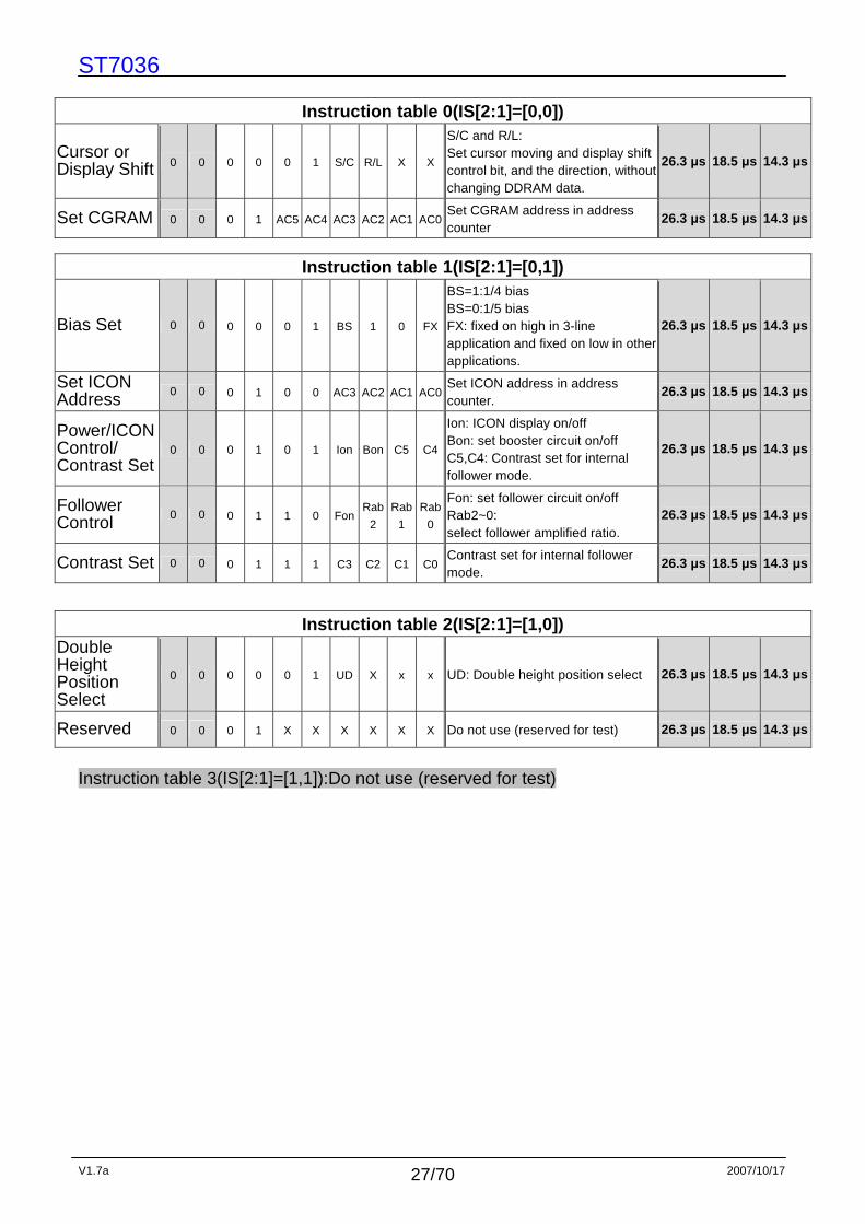
Instruction table 0(IS[2:1]=[0,0])
Cursor or Display Shift 0 0 0 0 0 1 S/C R/L X X
S/C and R/L: Set cursor moving and display shift control bit, and the direction, without changing DDRAM data.
26.3 µs 18.5 µs 14.3 µs
Set CGRAM 0 0 0 1 AC5 AC4 AC3 AC2 AC1 AC0 Set CGRAM address in address counter
26.3 µs 18.5 µs 14.3 µs
Instruction table 1(IS[2:1]=[0,1])
Bias Set 0 0 0 0 0 1 BS 1 0 FX
BS=1:1/4 bias BS=0:1/5 bias FX: fixed on high in 3-line application and fixed on low in other applications.
26.3 µs 18.5 µs 14.3 µs
Set ICON Address 0 0 0 1 0 0 AC3 AC2 AC1 AC0
Set ICON address in address counter.
26.3 µs 18.5 µs 14.3 µs
Power/ICON Control/ Contrast Set
0 0 0 1 0 1 Ion Bon C5 C4
Ion: ICON display on/off Bon: set booster circuit on/off C5,C4: Contrast set for internal follower mode.
26.3 µs 18.5 µs 14.3 µs
Follower Control 0 0 0 1 1 0 Fon
Rab
2
Rab
1
Rab
0
Fon: set follower circuit on/off Rab2~0: select follower amplified ratio.
26.3 µs 18.5 µs 14.3 µs
Contrast Set 0 0 0 1 1 1 C3 C2 C1 C0 Contrast set for internal follower mode.
26.3 µs 18.5 µs 14.3 µs
Instruction table 2(IS[2:1]=[1,0])
Double Height Position Select
0 0 0 0 0 1 UD X x x UD: Double height position select 26.3 µs 18.5 µs 14.3 µs
Reserved 0 0 0 1 X X X X X X Do not use (reserved for test) 26.3 µs 18.5 µs 14.3 µs
Instruction table 3(IS[2:1]=[1,1]):Do not use (reserved for test)

ST7036
V1.7a 2007/10/17 28/70
Instruction Description Clear Display
Clear all the display data by writing "20H" (space code) to all DDRAM address, and set DDRAM address to
"00H" into AC (address counter). Return cursor to the original status, namely, bring the cursor to the left edge
on first line of the display. Make entry mode increment (I/D = "1").
Return Home
Return Home is cursor return home instruction. Set DDRAM address to "00H" into the address counter.
Return cursor to its original site and return display to its original status, if shifted. Contents of DDRAM does
not change.
Entry Mode Set
Set the moving direction of cursor and display.
I/D : Increment / decrement of DDRAM address (curso r or blink) When I/D = "High", cursor/blink moves to right and DDRAM address is increased by 1.
When I/D = "Low", cursor/blink moves to left and DDRAM address is decreased by 1.
* CGRAM operates the same as DDRAM, when read from or write to CGRAM.
S: Shift of entire display When DDRAM read (CGRAM read/write) operation or S = "Low", shift of entire display is not performed. If
S = "High" and DDRAM write operation, shift of entire display is performed according to I/D value (I/D =
"1" : shift left, I/D = "0" : shift right).
S I/D Description
H H Shift the display to the left
H L Shift the display to the right
00 00 00 00 10
R/WRS DB6DB7 DB4DB5 DB2DB3 DB0DB1
00 00 00 00 X1
R/WRS DB6DB7 DB4DB5 DB2DB3 DB0DB1
00 00 00 10 SI/D
R/WRS DB6DB7 DB4DB5 DB2DB3 DB0DB1
ST7036
V1.7a 2007/10/17 29/70
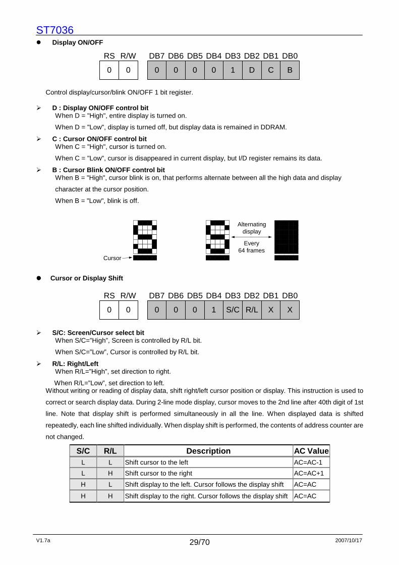
Display ON/OFF
Control display/cursor/blink ON/OFF 1 bit register.
D : Display ON/OFF control bit When D = "High", entire display is turned on.
When D = "Low", display is turned off, but display data is remained in DDRAM.
C : Cursor ON/OFF control bit When C = "High", cursor is turned on.
When C = "Low", cursor is disappeared in current display, but I/D register remains its data.
B : Cursor Blink ON/OFF control bit When B = "High", cursor blink is on, that performs alternate between all the high data and display
character at the cursor position.
When B = "Low", blink is off.
Cursor or Display Shift
S/C: Screen/Cursor select bit
When S/C=”High”, Screen is controlled by R/L bit.
When S/C=”Low”, Cursor is controlled by R/L bit.
R/L: Right/Left When R/L=”High”, set direction to right.
When R/L=”Low”, set direction to left. Without writing or reading of display data, shift right/left cursor position or display. This instruction is used to
correct or search display data. During 2-line mode display, cursor moves to the 2nd line after 40th digit of 1st
line. Note that display shift is performed simultaneously in all the line. When displayed data is shifted
repeatedly, each line shifted individually. When display shift is performed, the contents of address counter are
not changed.
S/C R/L Description AC Value L L Shift cursor to the left AC=AC-1
L H Shift cursor to the right AC=AC+1
H L Shift display to the left. Cursor follows the display shift AC=AC
H H Shift display to the right. Cursor follows the display shift AC=AC
Every64 frames
Alternatingdisplay
Cursor
00 00 00 D1 BC
R/WRS DB6DB7 DB4DB5 DB2DB3 DB0DB1
00 00 10 R/LS/C XX
R/WRS DB6DB7 DB4DB5 DB2DB3 DB0DB1

ST7036
V1.7a 2007/10/17 30/70
Function Set
00 00 DL1 DHN IS1IS2
R/WRS DB6DB7 DB4DB5 DB2DB3 DB0DB1
DL : Interface data length control bit When DL = "High", it means 8-bit bus mode with MPU.
When DL = "Low", it means 4-bit bus mode with MPU. So to speak, DL is a signal to select
8-bit or 4-bit bus mode.
When 4-bit bus mode, it needs to transfer 4-bit data by two times.
N : Display line number control bit When N = "High", 2-line display mode is set.
When N = "Low", it means 1-line display mode.
When “N3” option pin connect to VDD, N must set “N=1”.
DH : Double height font type control bit When DH = " High " and N= “Low”, display font is selected to double height mode(5x16 dot),RAM address
can only use 00H~27H.
When DH= “High” and N= “High”, it is forbidden.
When DH = " Low ", display font is normal (5x8 dot).
EXT option pin connect to high
EXT option pin connect to low N DH
Display Lines Character Font Display Lines Character
Font L L 1 5x8 1 5x8 L H 1 5x8 1 5x16 H L 2 5x8 2 5x8 H H 2 5x8 Forbidden
2 line mode normal display (DH=0/N=1)
1 line mode with double height font (DH=1/N=0)

ST7036
V1.7a 2007/10/17 31/70
IS[2:1]: instruction table select When IS[2:1]=(0,0): normal instruction be selected(refer instruction table 0)
When IS[2:1]=(0,1):extension instruction be selected(refer instruction table 1 )
When IS[2:1]=(1,0):extension instruction be selected(refer instruction table 2 )
When IS[2:1]=(1,1):Do not use (reserved for test)
Double height position set: IS[2:1]=(1,0)
00 00 10 XUD XX
R/WRS DB6DB7 DB4DB5 DB2DB3 DB0DB1
UD: Select double height font display position of scree n.(N3=VDD)
When UD = "High", double height font is show on Com1~Com16.
When UD = "Low", double height font is show on Com9~Com24.
DH UD 2 LINES(N3=VSS) 3 LINES(N3=VDD)
H H Com1~Com16 Double Height Com1~Com16 Double Height Com17~Com24 Normal Display
H L Com1~Com16 Double Height Com1~Com8 Normal Display Com9~Com24 Double Height
L X Normal Display Normal Display
00 10 00 AC2AC3 AC0AC1
R/WRS DB6DB7 DB4DB5 DB2DB3 DB0DB1

ST7036
V1.7a 2007/10/17 32/70
3 Line mode normal display (DH = 0 / N = 1 / UD = don`t care )
COM1 ..8 is normal , COM9 .. 24 is a double height font (DH = 1 / N = 1 / UD = 0 )
COM17 ..24 is normal , COM1 .. 16 is a double height font (DH = 1 / N = 1 / UD = 1 )

ST7036
V1.7a 2007/10/17 33/70
Set CGRAM Address
Set CGRAM address to AC.
This instruction makes CGRAM data available from MPU.
Set DDRAM Address
Set DDRAM address to AC.
This instruction makes DDRAM data available from MPU.
When 1-line display mode (N = 0), DDRAM address is from "00H" to "4FH".
In 2-line display mode (N = 1), DDRAM address in the 1st line is from "00H" to "27H", and
DDRAM address in the 2nd line is from "40H" to "67H".
In 3-line display mode (N3=1, N=1), DDRAM address in the 1st line is from “00H” to “OFH”, DDRAM in the
2nd line is from “10H” to “1FH”, and DDRAM in the 3rd line is from “20H” to “2FH”.
Read Busy Flag and Address
When BF = “High”, indicates that the internal operation is being processed. So during this time the next
instruction cannot be accepted.
The address Counter (AC) stores DDRAM/CGRAM addresses, transferred from IR.
After writing into (reading from) DDRAM/CGRAM, AC is automatically increased (decreased) by 1.
Write Data to CGRAM,DDRAM or ICON RAM
Write binary 8-bit data to CGRAM,DDRAM or ICON RAM
The selection of RAM from DDRAM, CGRAM or ICON RAM, is set by the previous address set instruction
: DDRAM address set, CGRAM address set, ICON RAM address set. RAM set instruction can also determine
the AC
direction to RAM.
After write operation, the address is automatically increased/decreased by 1, according to
the entry mode.
00 10 AC4AC5 AC2AC3 AC0AC1
R/WRS DB6DB7 DB4DB5 DB2DB3 DB0DB1
00 AC61 AC4AC5 AC2AC3 AC0AC1
R/WRS DB6DB7 DB4DB5 DB2DB3 DB0DB1
10 AC6BF AC4AC5 AC2AC3 AC0AC1
R/WRS DB6DB7 DB4DB5 DB2DB3 DB0DB1
01 D6D7 D4D5 D2D3 D0D1
R/WRS DB6DB7 DB4DB5 DB2DB3 DB0DB1

ST7036
V1.7a 2007/10/17 34/70
Read Data from CGRAM,DDRAM or ICON RAM
Read binary 8-bit data from DDRAM/CGRAM./ICON RAM
The selection of RAM is set by the previous address set instruction. If address set instruction of RAM is not
performed before this instruction, the data that read first is invalid, because the direction of AC is not
determined. If you read RAM data several times without RAM address set instruction before read operation,
you can get correct RAM data from the second, but the first data would be incorrect, because there is no time
margin to transfer RAM data.
Bias Set
BS: bias selection
When BS=”High”, the bias will be 1/4
When BS=”Low”, the bias will be 1/5
BS will be invalid when external bias resistors are used(OPF1=1,OPF2=1)
FX: must be fixed on high in 3-line application and fixed on low in other applications.
Set ICON RAM address
Set ICON RAM address to AC.
This instruction makes ICON data available from MPU.
When IS=1 at Extension mode,
The ICON RAM address is from "00H" to "0FH".
11 D6D7 D4D5 D2D3 D0D1
R/WRS DB6DB7 DB4DB5 DB2DB3 DB0DB1

ST7036
V1.7a 2007/10/17 35/70
Power/ICON control/Contrast set(high byte)
Ion: set ICON display on/off
When Ion = "High", ICON display on.
When Ion = "Low", ICON display off.
Bon: switch booster circuit Bon can only be set when internal follower is used (OPF1=0,OPF2=0).
When Bon = "High", booster circuit is turn on.
When Bon = "Low", booster circuit is turn off.
C5,C4 : Contrast set(high byte) C5,C4,C3,C2,C1,C0 can only be set when internal follower is used (OPF1=0,OPF2=0).They can more precisely adjust the input reference voltage of V0 generator. The details please refer to the supply voltage for LCD driver.
Follower control
Fon: switch follower circuit
Fon can only be set when internal follower is used (OPF1=0,OPF2=0). When Fon = "High", internal follower circuit is turn on.
When Fon = "Low", internal follower circuit is turn off.
Note that Fon must be set to “Low” if (OPF1, OPF2) is not (0,0).
Rab2,Rab1,Rab0 : V0 generator amplified ratio
Rab2,Rab1,Rab0 can only be set when internal follower is used (OPF1=0,OPF2=0).They can adjust the
amplified ratio of V0 generator. The details please refer to the supply voltage for LCD driver.
Contrast set(low byte)
C3,C2,C1,C0:Contrast set(low byte)
C5,C4,C3,C2,C1,C0 can only be set when internal follower is used (OPF1=0,OPF2=0).They can more precisely adjust the input reference voltage of V0 generator. The details please refer to the supply voltage for LCD driver.
00 10 10 BONION C4C5
R/WRS DB6DB7 DB4DB5 DB2DB3 DB0DB1
00 10 01Rab
2FON
Rab0
Rab1
R/WRS DB6DB7 DB4DB5 DB2DB3 DB0DB1
00 10 11 C2C3 C0C1
R/WRS DB6DB7 DB4DB5 DB2DB3 DB0DB1
ST7036
V1.7a 2007/10/17 36/70
Reset Function
Initializing by Internal Reset Circuit
An internal reset circuit automatically initializes the ST7036 when the power is turned on. The
following instructions are executed during the initialization. The busy flag (BF) is kept in the busy state (BF = 1)
until the initialization ends. The busy state lasts for 40 ms after VDD rises to stable.
1. Display clear
2. Function set:
DL = 1; 8-bit interface data
N = 0; 1-line display
DH=0; normal 5x8 font
IS[2:1]=(0,0); use instruction table 0
3. Display on/off control:
D = 0; Display off
C = 0; Cursor off
B = 0; Blinking off
4. Entry mode set:
I/D = 1; Increment by 1
S = 0; No shift
5. 3 line: FX=1
1/2 line: FX=0
6. ICON control
Ion=0; ICON off
7. Power control
BS=0; 1/5bias
Bon=0; booster off
Fon=0; follower off
(C5,C4,C3,C2,C1,C0)=(1,0,0,0,0,0)
(Rab2,Rab1,Rab0)=(0,1,0)
8. Double Height Position Select
UD=0, double height font is show on Com9~Com24.
Note: If the electrical characteristics conditions listed under the table Power Supply Conditions Using Internal Reset Circuit are not met, the internal reset circuit will not operate normally and will fail to initialize the ST7036. When internal Reset Circuit not operate,ST7036 can be reset by XRESET pin from MPU control signal.

ST7036
V1.7a 2007/10/17 37/70
Initializing by Instruction 8-bit Interface (fosc=380kHz)
P O W E R O N o r e x te rn a l re s e t
W a it t im e > 4 0 m SA fte r V D D s ta b le
W a it t im e > 2 6 .3 μμμμ S
F u n c t io n s e tR S R /W D B 7 D B 6 D B 5 D B 4 D B 3 D B 2 D B 1 D B 00 0 0 0 1 1 N D H IS 2 IS 1
F u n c t io n s e tR S R /W D B 7 D B 6 D B 5 D B 4 D B 3 D B 2 D B 1 D B 00 0 0 0 1 1 N D H IS 2 IS 1
W a it t im e > 2 6 .3 μμμμ S
W a it t im e > 2 6 .3 μμμμ S
In itia liz a tio n e n d
B F c a n n o t b ec h e c k e d b e fo reth is in s tru c tio n .
B F c a n n o t b ec h e c k e d b e fo reth is in s tru c tio n .
W a it t im e > 2 6 .3 μμμμ S
W a it t im e > 2 6 .3 μμμμ S
W a it t im e > 2 6 .3 μμμμ S
P o w e r/IC O N /C o n tra s t c o n tro lR S R /W D B 7 D B 6 D B 5 D B 4 D B 3 D B 2 D B 1 D B 00 0 0 1 0 1 Io n B o n C 5 C 4
F o llo w e r c o n tro lR S R /W D B 7 D B 6 D B 5 D B 4 D B 3 D B 2 D B 1 D B 00 0 0 1 1 0 F o n R a b 2 R a b 1 R a b 0
D is p la y O N /O F F c o n tro lR S R /W D B 7 D B 6 D B 5 D B 4 D B 3 D B 2 D B 1 D B 00 0 0 0 0 0 1 D C B
B ia s S e tR S R /W D B 7 D B 6 D B 5 D B 4 D B 3 D B 2 D B 1 D B 00 0 0 0 0 1 B S 1 0 F X
W a it t im e > 2 6 .3 μμμμ S
C o n tra s t s e tR S R /W D B 7 D B 6 D B 5 D B 4 D B 3 D B 2 D B 1 D B 00 0 0 1 1 1 C 3 C 2 C 1 C 0

ST7036
V1.7a 2007/10/17 38/70
Initial Program Code Example For 8051 MPU(8 Bit Int erface): ;--------------------------------------------------------------------------------- INITIAL_START:
CALL DELAY40mS MOV A,#38H ;FUNCTION SET CALL WRINS_NOCHK ;8 bit, N=1,5*7dot CALL DELAY30uS MOV A,#38H ;FUNCTION SET CALL WRINS_NOCHK ;8 bit, N=1,5*7dot CALL DELAY30uS MOV A,#14H ;set bias CALL WRINS_CHK CALL DELAY30uS MOV A,#78H ;Contrast set adjustment CALL WRINS_CHK CALL DELAY30uS MOV A,#5EH ;Power/ICON/Contrast control CALL WRINS_CHK CALL DELAY30uS MOV A,#6AH ;Follower control CALL WRINS_CHK CALL DELAY30uS MOV A,#0CH ;DISPLAY ON CALL WRINS_CHK CALL DELAY30uS MOV A,#01H ;CLEAR DISPLAY CALL WRINS_CHK CALL DELAY2mS MOV A,#06H ;ENTRY MODE SET CALL WRINS_CHK ;CURSOR MOVES TO RIGHT CALL DELAY30uS
;--------------------------------------------------------------------------------- MAIN_START:
XXXX XXXX XXXX XXXX
;--------------------------------------------------------------------------------- WRINS_CHK:
CALL CHK_BUSY WRINS_NOCHK:
CLR RS ;EX: Port 3.0 CLR RW ;EX: Port 3.1 SETB E ;EX:Port 3.2 MOV P1,A ;EX:Port 1=Data Bus CLR E MOV P1,#FFH ;For Check Busy Flag RET
;--------------------------------------------------------------------------------- CHK_BUSY: ;Check Busy Flag
CLR RS SETB RW SETB E JB P1.7,$ CLR E RET

ST7036
V1.7a 2007/10/17 39/70
4-bit Interface (fosc=380kHz)

ST7036
V1.7a 2007/10/17 40/70
Initial Program Code Example For 8051 MPU(4 Bit Int erface): ;------------------------------------------------------------------- INITIAL_START:
CALL DELAY40mS MOV A,#30H ; FUNCTION SET CALL WRINS_ONCE ; 8 bit, DL = 1 CALL DELAY2mS MOV A,#30H ; FUNCTION SET CALL WRINS_ONCE ; 8 bit, DL = 1 CALL DELAY30uS MOV A,#30H ; FUNCTION SET CALL WRINS_ONCE ; 8 bit, DL = 1 CALL DELAY30uS CALL CHK_BUSY MOV A,#20H ; FUNCTION SET CALL WRINS_ONCE ; 4 bit, DL = 0 CALL DELAY30uS MOV A,#29H ; FUNCTION SET CALL WRINS_CHK ; 4 bit, DL = 0, N = 1, CALL DELAY30uS ; IS2 = 0, IS1 = 1 MOV A,#14H ;bias CALL WRINS_CHK CALL DELAY30uS MOV A,#78H ;Contrast set CALL WRINS_CHK CALL DELAY30uS MOV A,#5EH ;Power/ICON/Contrast CALL WRINS_CHK CALL DELAY30uS MOV A,#6AH ;Follower control CALL WRINS_CHK CALL DELAY30uS MOV A,#0CH ;DISPLAY ON CALL WRINS_CHK CALL DELAY30uS MOV A,#01H ;CLEAR DISPLAY CALL WRINS_CHK CALL DELAY2mS MOV A,#06H ;ENTRY MODE SET CALL WRINS_CHK CALL DELAY30uS
;------------------------------------------------------------------- MAIN_START:
XXXX XXXX XXXX
XXXX ;------------------------------------------------------------------- WRINS_CHK:
CALL CHK_BUSY WRINS_NOCHK:
PUSH A ANL A,#F0H CLR RS ;EX: Port 3.0 CLR RW ;EX: Port 3.1 SETB E ;EX: Port 3.2 MOV P1,A ;EX:Port1=Data Bus CLR E POP A SWAP A
WRINS_ONCE: ANL A,#F0H CLR RS CLR RW SETB E MOV P1,A CLR E MOV P1,#FFH ;For Check Bus Flag RET
;------------------------------------------------------------------- CHK_BUSY: ;Check Busy Flag
PUSH A MOV P1,#FFH
$1 CLR RS SETB RW SETB E MOV A,P1 CLR E MOV P1,#FFH CLR RS SETB RW SETB E NOP CLR E JB A.7,$1 POP A RET

ST7036
V1.7a 2007/10/17 41/70
Serial interface & IIC interface ( fosc = 380kHz )
ST7036
V1.7a 2007/10/17 42/70
Initial Program Code Example For 8051 MPU ( Serial Interface ) : ;--------------------------------------------------------------------------------- INITIAL_START:
CALL HARDWARE_RESET CALL DELAY40mS MOV A,#38H ;FUNCTION SET CALL WRINS_NOCHK ;8 bit, N=1,5*7dot CALL DELAY30uS MOV A,#39H ;FUNCTION SET CALL WRINS_NOCHK ;8 bit, N=1,5*7dot,IS=1 CALL DELAY30uS MOV A,#14H ;bias CALL WRINS_NOCHK CALL DELAY30uS MOV A,#78H ;Contrast set CALL WRINS_NOCHK CALL DELAY30uS MOV A,#5EH ;Power/ICON/Contrast control CALL WRINS_NOCHK CALL DELAY30uS MOV A,#6AH ;Follower control CALL WRINS_NOCHK CALL DELAY200mS ;for power stable MOV A,#0CH ;DISPLAY ON CALL WRINS_NOCHK CALL DELAY30uS MOV A,#01H ;CLEAR DISPLAY CALL WRINS_NOCHK CALL DELAY2mS MOV A,#06H ;ENTRY MODE SET CALL WRINS_NOCHK ;CURSOR MOVES TO RIGHT CALL DELAY30uS
;--------------------------------------------------------------------------------- MAIN_START:
XXXX XXXX XXXX XXXX . . .
;--------------------------------------------------------------------------------- WRINS_NOCHK:
PUSH 1 MOV R1,#8 CLR RS
$1 RLC A MOV SI,C SETB SCL NOP CLR SCL DJNZ R1,$1 POP 1 CALL DLY1.5mS RET

ST7036
V1.7a 2007/10/17 43/70
Interfacing to the MPU
The ST7036 can send data in two 4-bit operations/one 8-bit operation, serial 1 bit operation or fast I2C operation,
thus allowing interfacing with 4-bit, 8-bit or I2C MPU.
For 4-bit interface data, only four bus lines (DB4 to DB7) are used for transfer. Bus lines DB0 to DB3
are disabled. The data transfer between the ST7036 and the MPU is completed after the 4-bit data has been
transferred twice. As for the order of data transfer, the four high order bits (for 8-bit operation, DB4 to DB7)
are transferred before the four low order bits (for 8-bit operation, DB0 to DB3). The busy flag must be
checked (one instruction) after the 4-bit data has been transferred twice. Two more 4-bit operations then
transfer the busy flag and address counter data.
Example of busy flag check timing sequence
Intel 8051 interface(4 Bit)
Functioning
DB7
Internaloperation
E
R/W
RS
Busy flag check Busy flag check Instruction writeInstruction write
IR7 IR3 AC3Not
BusyAC3 IR3IR7
CSB
P1.0 to P1.3
P3.0P3.1P3.2
RSR/WE
DB4 to DB7
COM1 toCOM16/24
SEG1 toSEG100/80
100/80
16/24
Intel 8051 Serial ST7036
4
P3.3 CSB

ST7036
V1.7a 2007/10/17 44/70
For 8-bit interface data, all eight bus lines (DB0 to DB7) are used.
Example of busy flag check timing sequence
Intel 8051 interface(8 Bit)
DataNot
BusyBusyBusy Data
Functioning
DB7
Internaloperation
E
R/W
RS
Busy flagcheck
Busy flagcheck
Busy flagcheck
Instructionwrite
Instructionwrite
CSB
P1.0 to P1.7
P3.0P3.1P3.2
RSR/WE
DB0 to DB7
COM1 toCOM16/24
SEG1 toSEG100/80
100/80
16/24
Intel 8051 Serial ST7036
8
CSBP3.3

ST7036
V1.7a 2007/10/17 45/70
For serial interface data, only two bus lines (DB6 to DB7) are used.
Example of timing sequence
Intel 8051 interface ( Serial 4-line )
1 2 3 4 5 6 7 8 9 10 11 12 13 14
D7 D6 D5 D4 D3 D2 D1 D0 D7 D6 D5 D4 D3 D2
CSB
SI
SCL
RS
P1.6 to P1.7
P3.0P3.3
RSCSB
SI , SCL
COM1 toCOM16/24
SEG1 toSEG100/80
100/80
16/24
Intel 8051 Serial ST7036
2
ST7036
V1.7a 2007/10/17 46/70
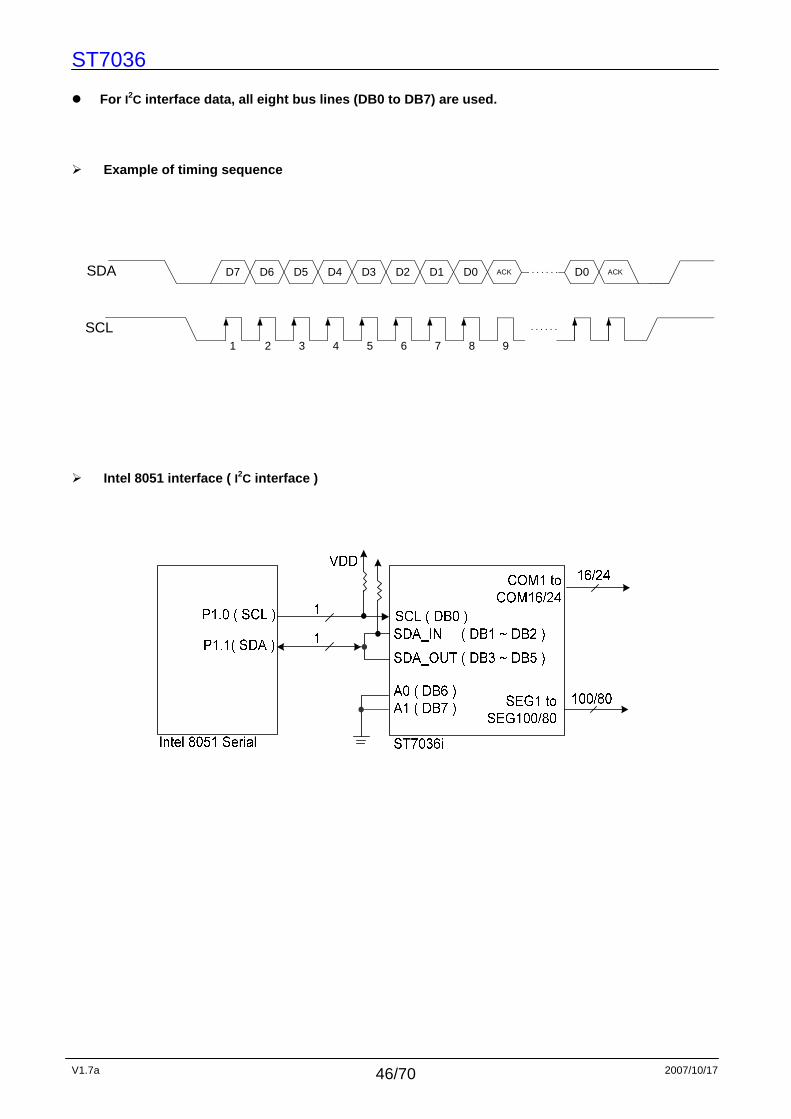
For I2C interface data, all eight bus lines (DB0 to DB7) a re used.
Example of timing sequence
Intel 8051 interface ( I2C interface )
SCL1 2 3 4 5 6 7 8 9
SDA D7 D6 D5 D4 D3 D2 D1 D0 ACK D0 ACK
. . . . . .
. . . . . . .

ST7036
V1.7a 2007/10/17 47/70
Supply Voltage for LCD Drive
When external bias resistors are used
(OPF1=1,OPF2=1)
When built-in bias resistors(9.6K Ω) are used
(OPF1=1,OPF2=0)
Note: Do not use built-in booster while built-in bi as resistors are used.
R
R
R
GND
Vext
1/5 bias
VR
R
VDD
V0
V1
V2
V3
V4
OPF1 OPF2
CAP1P
CAP1N
VSS
VLCD
VCC (2.7~ 5.5V)
R
R
R
Vext
1/4 bias
R
VR
VDD
V0
V1
V2V3
V4
OPF1 OPF2
CAP1P
CAP1N
VSS
VLCD
GND
VCC (2.7~ 5.5V)
VOUT
VIN
VOUT
VIN
GND
Vext
VRVDD
V0
V1
V2
V3
V4
OPF1
OPF2
CAP1P
CAP1N
VSS
VLCD
VCC(2.7~5.5V)
VOUT
VIN

ST7036
V1.7a 2007/10/17 48/70
When built-in bias resistors(3.3K Ω) are used
(OPF1=0,OPF2=1)
Note: Do not use built-in booster while built-in bi as resistors are used.
When built-in voltage followers with external Vout are used
(OPF1=0,OPF2=0 and instruction setting Bon=0,Fon=1)
GND
Vext
VRVDD
V0
V1
V2
V3
V4
OPF2
OPF1
CAP1P
CAP1N
VSS
VLCD
VCC (2.7~ 5.5V)
VOUT
VIN
GND
VLCD
VCC (2.7~ 5.5V)
OPF1 OPF2
Vext ≧ V0
VDD
V0
V1
V2
V3
V4
CAP1P
CAP1N
VSS
VIN
VOUT
Don't need to connect stable capacitor whenuse internal follower circuit
ST7036
V1.7a 2007/10/17 49/70
GND
VDD
V0
V1
V2
V3
V4
VOUT
CAP1P
CAP1N
VSS
VLCD
VCC (2.7~ 3.5V)
OPF1 OPF2
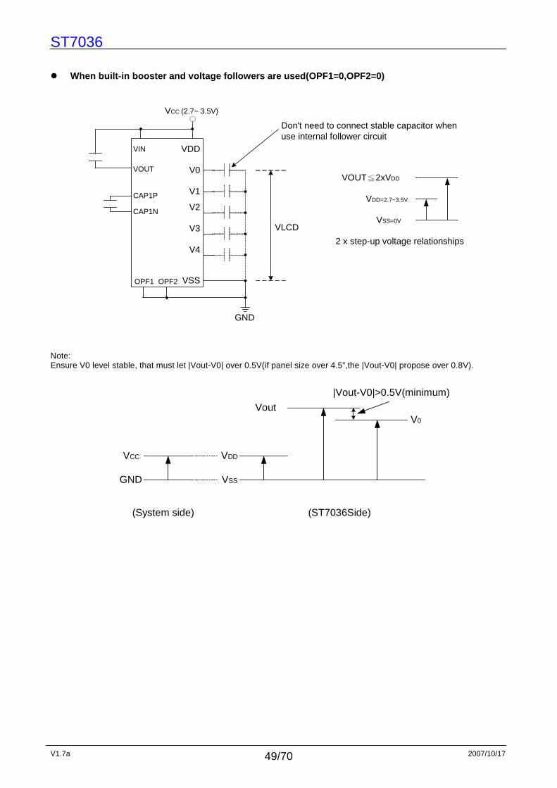
VOUT≦2xVDD
VSS=0V
VDD=2.7~3.5V
2 x step-up voltage relationships
VIN
Don't need to connect stable capacitor whenuse internal follower circuit
When built-in booster and voltage followers are use d(OPF1=0,OPF2=0)
Note: Ensure V0 level stable, that must let |Vout-V0| over 0.5V(if panel size over 4.5”,the |Vout-V0| propose over 0.8V).
(System side) (ST7036Side)
Vout
VDD
VSS
VCC
GND
V0
|Vout-V0|>0.5V(minimum)

ST7036
V1.7a 2007/10/17 50/70
V0 voltage follower value calculation
C5 C4 C3 C2 C1 C0 α Rab2 Rab1 Rab0 1+Rb/Ra
0 0 0 0 0 0 0 0 0 0 1
0 0 0 0 0 1 1 0 0 1 1.25
0 0 0 0 1 0 2 0 1 0 1.5
0 1 1 1.8 : :
: : 1 0 0 2
1 1 1 1 0 1 61 1 0 1 2.5
1 1 1 1 1 0 62 1 1 0 3
1 1 1 1 1 1 63 1 1 1 3.75
V0 level (Condition:Booster on, Follower on, VIN=3.5V, VDD=3.0V,Display off)
The recommended curve: follower = 04H
Notes:
1. Vout ≧V0 ≧V1 ≧V2 ≧V3 ≧V4 ≧Vss must be maintained.
2. If the calculation value of V0 is higher than Vout, the real V0 value will saturate to Vout.
3. internal built-in booster can only be used when OPF1=0,OPF2=0.
Vref
V0
Vout(≧VDD)VDD
RaRb
VSS
) VrefRbRa
V0=(1+ x
While Vref=VDD (α+36
100)x
0
1
2
3
4
5
6
7
8
1 3 5 7 9 11 13 15 17 19 21 23 25 27 29 31 33 35 37 39 41 43 45 47 49 51 53 55 57 59 61 63
ST7036
V1.7a 2007/10/17 51/70
0
1
2
3
4
5
6
7
8
0 2 4 6 8 10 12 14 16 18 20 22 24 26 28 30 32 34 36 38 40 42 44 46 48 50 52 54 56 58 60 62
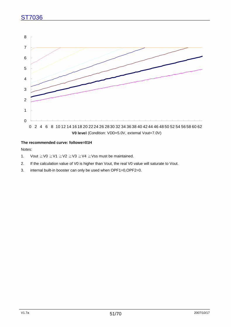
V0 level (Condition: VDD=5.0V, external Vout=7.0V)
The recommended curve: followe=01H
Notes:
1. Vout ≧V0 ≧V1 ≧V2 ≧V3 ≧V4 ≧Vss must be maintained.
2. If the calculation value of V0 is higher than Vout, the real V0 value will saturate to Vout.
3. internal built-in booster can only be used when OPF1=0,OPF2=0.

ST7036
V1.7a 2007/10/17 52/70
AC Characteristics 68 Interface
( Ta =-35°C to 85°C ) VDD=2.7 to 4.5V
Rating VDD=4.5 to 5.5V
Rating Item Signal Symbol Condition
Min. Max. Min. Max. Units
Address hold time RS tAH6 20 - 20 -
Address setup time RS tAW6 —
20 - 20 - ns
System cycle time RS tCYC6 — 400 - 280 - ns
Data setup time D0 to D7 tDS6 100 - 80 -
Data hold time D0 to D7 tDH6 —
40 - 20 - ns
Access time D0 to D7 tACC6 - 500 - 400
Output disable time D0 to D7 tOH6 CL = 100 pF
300 - 150 - ns
Enable H pulse time E tEWH — 200 - 120 - ns
Enable L pulse time E tEWL — 150 - 130 - ns
Note: All timing is specified using 20% and 80% of VDD as the reference.
tAW6 tAH6
tDS6 tDH6
tACC6 tOH6
tEWH
tCYC6
tEWL
RSR/W
E
D0 to D7(Write)
D0 to D7(Read)
CSB

ST7036
V1.7a 2007/10/17 53/70
Serial Interface
( Ta =-35°C to 85°C )
VDD=2.7 to 4.5V Rating
VDD=4.5 to 5.5V Rating Item Signal Symbol Condition
Min. Max. Min. Max. Units
Serial Clock Period tSCYC 200 - 100 -
SCL “H” pulse width tSHW 20 - 20 -
SCL “L” pulse width
SCL
tSLW
—
160 - 120 -
ns
Address setup time tSAS 10 - 10 -
Address hold time RS
tSAH —
250 - 150 - ns
Data setup time tSDS 10 - 10 -
Data hold time SI
tSDH —
10 - 20 - ns
tCSS 20 - 20 - CS-SCL time CS
tCSH —
350 - 200 - ns
*1 All timing is specified using 20% and 80% of VDD as the standard.
tCSS tCSH
tSDS tSDH
tSLW
tSCYC
tSHW
RS
SCL
SI
tSAS tSAH
CSB

ST7036
V1.7a 2007/10/17 54/70
I2C interface
( Ta =-35°C to 85°C ) VDD=2.7 to 4.5V
Rating VDD=4.5 to 5.5V
Rating Item Signal Symbol Condition Min. Max. Min. Max.
Units
SCL clock frequency fSCLK DC 300K DC 400 kHz
SCL clock low period tLOW 2.5 — 1.3 —
SCL clock high period
SCL
tHIGH
—
0.6 — 0.6 — µs
Data set-up time tSU;DAT 1800 — 700 — ns
Data hold time SDA
tHD:DAT —
0 — 0 0.5 µs
SCL,SDA rise time tr 20+0.1Cb 300 20+0.1Cb 300
SCL,SDA fall time
SCL, SDA tf
— 20+0.1Cb 300 20+0.1Cb 300
ns
Capacitive load represent by each bus line
Cb — — 400 — 400 pf
Setup time for a repeated START condition
tSU;STA — 0.6 — 0.6 — µs
Start condition hold time SDA
tHD;STA — 1.8 — 1.0 — µs
Setup time for STOP condition tSU;STO — 0.6 — 0.6 — µs
Bus free time between a Stop and START condition SCL tBUF — 1.3 — 1.3 — µs
SDA
SCL
tBUF
tDH;STA
tLOW
tHD;DAT
tHIGH
tr
tf
tSU;DAT
tSU;STOtSU;STA
SDA

ST7036
V1.7a 2007/10/17 55/70
2.7V/4.5V
0.2V 0.2V 0.2V
trcc tOFF
tOFF≧1mS0.1mS≦trcc≦10mS
Notes: tOFF compensates for the power oscillation period caused by momentary power supply
oscillations. Specified at 4.5V for 5V operation, and at 2.7V for 3V operation. For if 2.7V/4.5V is not reached during 3V/5V operation, internal reset circuit will not
operate normally.
2.7V/4.5V
0.2V
tr 100nS≦
tL>100uS
Internal Power Supply Reset
Hardware reset(XRESET)

ST7036
V1.7a 2007/10/17 56/70
Absolute Maximum Ratings
Characteristics Symbol Value Power Supply Voltage VDD -0.3 to +6.0
LCD Driver Voltage VLCD 7.0- Vss to -0.3+Vss
Input Voltage VIN -0.3 to VDD+0.3
Operating Temperature TA -30oC to + 85oC
Storage Temperature TSTO -65oC to + 150oC
DC Characteristics (VDD = 2.7 V, TA =-35 to 85)
Symbol Characteristics Test Condition Min. Typ. Max. Unit
VDD Operating Voltage - 2.7 - 4.5 V
VLCD LCD Voltage V0-Vss 2.7 - 7.0 V
VIN Power Supply - - - 3.5 V
IDD Power Supply Current VDD=3.0V
(Use internal booster/follower circuit)
- 160 230 uA
VIH1 Input High Voltage
(Except OSC1) -
0.7 VDD
- VDD V
VIL1 Input Low Voltage
(Except OSC1) - - 0.3 - 0.8 V
VIH2 Input High Voltage
(OSC1) -
0.7 VDD
- VDD V
VIL2 Input Low Voltage
(OSC1) - - -
0.2 VDD
V
VOH Output High Voltage
(DB0 - DB7) IOH = -1.0mA
0.7 VDD
- - V
VOL Output Low Voltage
(DB0 - DB7) IOL = 1.0mA - - 0.8 V
RCOM Common Resistance VLCD = 4V, Id = 0.05mA - 2 20 KΩ
RSEG Segment Resistance VLCD = 4V, Id = 0.05mA - 2 30 KΩ
ILEAK Input Leakage
Current VIN = 0V to VDD -1 - 1 µA
IPUP Pull Up MOS Current VDD = 3V 20 30 40 µA
fOSC Oscillation frequency VDD = 3V,1/17duty 350 540 1100 kHz

ST7036
V1.7a 2007/10/17 57/70
DC Characteristics
(VDD = 4.5 V ,TA = -35 to 85)
Symbol Characteristics Test Condition Min. Typ. Max. Unit
VDD Operating Voltage - 4.5 - 5.5 V
VLCD LCD Voltage V0-Vss 2.7 - 7.0 V
VIN Power Supply - - - 3.5 V
IDD Power Supply Current VDD=5.0V
(Use internal booster/follower circuit)
- 240 340 µA
VIH1 Input High Voltage
(Except OSC1) -
0.7 VDD
- VDD V
VIL1 Input Low Voltage
(Except OSC1) - -0.3 - 0.8 V
VIH2 Input High Voltage
(OSC1) -
0.7 VDD
- VDD V
VIL2 Input Low Voltage
(OSC1) - - - 1.0 V
VOH Output High Voltage
(DB0 - DB7) IOH = -1.0mA
0.8 VDD
- VDD V
VOL Output Low Voltage
(DB0 - DB7) IOL = 1.0mA - - 0.8 V
RCOM Common Resistance VLCD = 4V, Id = 0.05mA - 2 20 KΩ
RSEG Segment Resistance VLCD = 4V, Id = 0.05mA - 2 30 KΩ
ILEAK Input Leakage
Current VIN = 0V to VDD -1 - 1 µA
IPUP Pull Up MOS Current VDD = 5V 65 95 125 µA
fOSC Oscillation frequency VDD = 5V,1/17duty 350 540 1100 kHz

ST7036
V1.7a 2007/10/17 58/70
LCD Frame Frequency 1/16 Duty(ST7066U normal mode); Assume the oscillat ion frequency is 540KHZ, 1 clock cycle time
= 1.85us, 1/16 duty; 1/5 bias,1 frame =1.85us x 200 x 16 = 5.92ms=168.9Hz(SHLC and SHLS connect
to High)
1 2 3 4 16 1 2 3 4 16 1 2 3 4 16
V0 V1 V2
V3 V4 Vss
COM1
V0 V1 V2
V3 V4 Vss
COM2
V0 V1 V2
V3 V4 Vss
COM16
V0 V1 V2
V3 V4 Vss
SEGx off
V0 V1 V2
V3 V4 Vss
1 frame
SEGx on
200 clocks
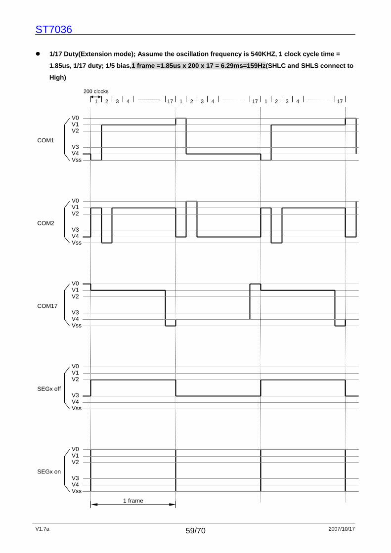
ST7036
V1.7a 2007/10/17 59/70
1/17 Duty(Extension mode); Assume the oscillation f requency is 540KHZ, 1 clock cycle time =
1.85us, 1/17 duty; 1/5 bias,1 frame =1.85us x 200 x 17 = 6.29ms=159Hz(SHLC and SHLS connect to
High)
1 2 3 4 17 1 2 3 4 17 1 2 3 4 17
V0 V1 V2
V3 V4 Vss
COM1
V0 V1 V2
V3 V4 Vss
COM2
V0 V1 V2
V3 V4 Vss
COM17
V0 V1 V2
V3 V4 Vss
SEGx off
V0 V1 V2
V3 V4 Vss
1 frame
SEGx on
200 clocks
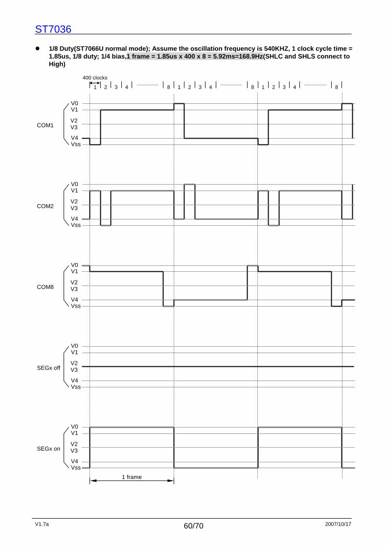
ST7036
V1.7a 2007/10/17 60/70
1/8 Duty(ST7066U normal mode); Assume the oscillati on frequency is 540KHZ, 1 clock cycle time =
1.85us, 1/8 duty; 1/4 bias,1 frame = 1.85us x 400 x 8 = 5.92ms=168.9Hz(SHLC and SHLS connect to High)
1 2 3 4 8 1 2 3 4 8 1 2 3 4 8
V0 V1
V2 V3
V4 Vss
COM1
V0 V1
V4 Vss
COM2
V0 V1
V4 Vss
COM8
V0 V1
V4 Vss
SEGx off
V0 V1
V4 Vss
1 frame
SEGx on
V2 V3
V2 V3
V2 V3
V2 V3
400 clocks

ST7036
V1.7a 2007/10/17 61/70
1/9 Duty(Extension mode); Assume the oscillation fr equency is 540KHZ, 1 clock cycle time =
1.85us, 1/9 duty; 1/4 bias,1 frame = 1.85us x 400 x 9 = 6.66ms=150Hz(SHLC and SHLS connect to High)
1 2 3 4 9 1 2 3 4 9 1 2 3 4 9
V0 V1
V2 V3
V4 Vss
COM1
V0 V1
V4 Vss
COM2
V0 V1
V4 Vss
COM9
V0 V1
V4 Vss
SEGx off
V0 V1
V4 Vss
1 frame
SEGx on
V2 V3
V2 V3
V2 V3
V2 V3
400 clocks

ST7036
V1.7a 2007/10/17 62/70
1/25 Duty( Extension mode and 3-line ); Assume the oscillation frequency is 540KHZ, 1 clock cycle
time = 1.85us, 1/25 duty; 1/4 bias,1 frame = 1.85us x 160 x 25 = 7.40ms=135.1Hz(SHLC and SHLS connect to High)
1 2 3 4 25 1 2 3 4 25 1 2 3 4 25
V0 V1
V2 V3
V4 Vss
COM1
V0 V1
V4 Vss
COM2
V0 V1
V4 Vss
COM25
V0 V1
V4 Vss
SEGx off
V0 V1
V4 Vss
1 frame
SEGx on
V2 V3
V2 V3
V2 V3
V2 V3
160 clocks

ST7036
V1.7a 2007/10/17 63/70
I/O Pad Configuration
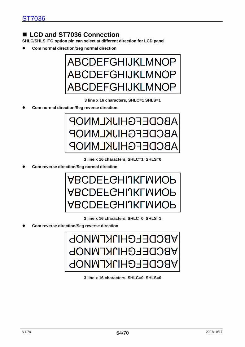
ST7036
V1.7a 2007/10/17 64/70
LCD and ST7036 Connection SHLC/SHLS ITO option pin can select at different di rection for LCD panel
Com normal direction/Seg normal direction
3 line x 16 characters, SHLC=1 SHLS=1
Com normal direction/Seg reverse direction
3 line x 16 characters, SHLC=1, SHLS=0
Com reverse direction/Seg normal direction
3 line x 16 characters, SHLC=0, SHLS=1
Com reverse direction/Seg reverse direction
3 line x 16 characters, SHLC=0, SHLS=0

ST7036
V1.7a 2007/10/17 65/70
Application Circuit ( Normal mode ) Use internal resistor(9.6K ohm) and contrast adjust with external VR. Booster always off. Has 240 character of CGROM. Internal oscillator.
Dot Matrix LCD Panel
ST7036
RS,R/W,E,CSB,DB0-DB7,XRESET
To MPU
Seg 1-80Com 1-24
OPF2
CLSSHLCSHLS
OPF1
OPR2
EXT
OPR1
VDD
V0
V4V3V2V1
CAP1PCAP1N
Vext
VOUTVIN
N3
VDD

ST7036
V1.7a 2007/10/17 66/70
Application Circuit(Extension mode) Use internal follower circuit. Booster has 2 times pump. Has 240 character of CGROM. Internal oscillator.
When the heavy load is applied, the dotted line part could be added.
Dot Matrix LCD Panel
ST7036
RS,R/W ,E,CSB,DB0-DB7,XRESET
To MPU
Seg 1-80Com 1-24
OPF2
CLSSHLCSHLS
OPF1
OPR2
EXT
OPR1
VDD
Vext
CAP1PCAP1N
V0
V4V3V2V1
VOUTVIN
N3

ST7036
V1.7a 2007/10/17 67/70
Application Circuit ( for glass layout ) ST7036 over Glass,6800 serial 8bit interface, with booster and follower circuit on
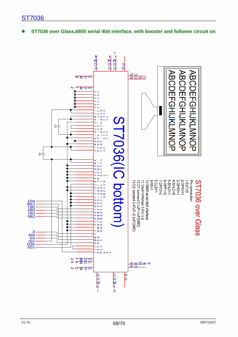
ST7036
V1.7a 2007/10/17 68/70
ST7036 over Glass,6800 serial 4bit interface, with booster and follower circuit on

ST7036
V1.7a 2007/10/17 69/70
ST7036 over Glass, serial interface, with booster and follower circuit on

ST7036
V1.7a 2007/10/17 70/70
ST7036 over Glass, I2C interface, with booster and follower circuit on In I2C application, note that the impedence of SDAs and GNDs should be keep in the POWER PIN LEVEL.

User’s Guide
LCD Safe Handling Procedure
______________________________
For product support, contact Newhaven Display International 2511 Technology Drive, #101 Elgin, IL 60124 Tel: (847)844-8795 Fax: (847)844-8796

USING LCD MODULES LIQUID CRYSTAL DISPLAY MODULES LCD’s are composed of glass, liquid crystal fluid, and a polarizer. Please pay attention to the following items when handling:
1. Keep the temperature within a specified range for use and storage. Polarization degradation, bubble generation or polarizer peel‐off may occur with high temperatures and high humidity.
2. Do not touch, push or rub the exposed polarizer with anything harder than an HB lead pencil (glass, tweezers, etc).
3. N‐hexane is recommended for cleaning the adhesives used to attach the front/rear polarizer. Reflectors made of organic substances will be damaged by chemicals such as acetone, toluene, ethanol and isopropyl alcohol.
4. If the display surface becomes contaminated, breathe on the surface and gently wipe it with a soft dry cloth. If it is heavily contaminated, wipe it gently with absorbent cotton or another soft material like a chamois soaked in Isopropyl alcohol or Ethyl alcohol. Scrub gently to avoid damaging the display surface.
5. Wipe off saliva or water immediately! Contact with water over a long period of time may cause deformation or color fading.
6. Avoid contact with oil or any greasy substances. 7. If there is condensation on the surface and contact with the terminals while cold, it will damage, stain
or dirty the polarizer. After the product is tested at a low temperature, they must be warmed up in a container before being exposed to room temperature environments.
8. Do not put or attach anything on the display area in order to avoid leaving marks. 9. Do not touch the display with bare hands. This will stain the display area and degrade the insulation
between terminals. (Some cosmetics are detrimental to the polarizer). 10. Exercise care to minimize corrosion of the electrode. Corrosion of the electrodes is accelerated by
water droplets, moisture condensation or a current flow in a high‐humidity environment. 11. As glass is fragile, care should be taken to avoid chipping, while handling the edges especially.
PRECAUTIONS FOR HANDLING LCD MODULES Since the LCD module has been assembled and adjusted with a high degree of precision, avoid applying excessive shock or force to the module or making any alterations or modifications to it.
1. Do not alter, modify or change the shape of the tab on the metal frame. 2. Do not make extra holes on the printed circuit board, modify its shape or change the positions of
components to be attached. 3. Do not damage or modify the pattern wiring on the printed circuit board. 4. Absolutely do not modify the zebra rubber strip (conductive rubber) or heat the seal connector! 5. Except for soldering the interface, do not make any alterations or modifications with a soldering iron. 6. Do not drop, bend or twist the LCD module. In particular, don’t forcibly pull or bend the I/O cable or
backlight cable.

7. In order to avoid cracking the FPC, pay attention to the area where the FPC is bent, the edge of the overlay, the area of the surface of Ni‐Au plating, the area of soldering land, and the area of the through hole.
ELECTRO‐STATIC DISCHARGE CONTROL Since this module uses a CMOS LSI, give the same careful attention to the electrostatic discharge as you would for an ordinary CMOS IC.
1. Make sure you are grounded when handling LCD modules. To minimize the performance degradation of the LCD modules resulting from destruction caused by static electricity, exercise care to avoid holding the following sections when handling the modules: exposed area of the printed circuit board, terminal electrode sections.
2. Before removing the LCD module from its packing case or incorporating it into a set, be sure the module and your body have the same electric potential.
3. When soldering the terminal of the LCD module, make sure the AC power source for the soldering iron does not leak.
4. When using an electric screwdriver to attach the LCD module, the screwdriver should be of ground potentiality, to minimize any transmission of electromagnetic waves producing sparks coming from the commutator of the motor.
5. As far as possible, make the electric potential of your work clothes and that of the work bench the ground potential.
6. To reduce the generation of static electricity, be careful that the air in the working environment is not too dry. (A relative humidity of 50‐60% is recommended).
PRECAUTIONS FOR OPERATION 1. Viewing angle varies with the change of liquid crystal driving voltage (VO). Adjust VO to show the
best contrast. 2. Driving the LCD in the voltage above the limit shortens its life. 3. If the LCD modules have been operating for a long time showing the same display patterns, the
display patterns may remain on the screen as ghost images and a slight contrast irregularity may also appear. A normal operating status can be regained by suspending use for some time. It should be noted that this phenomenon does not adversely affect performance reliability.
4. Response time is greatly delayed at temperatures below the operating temperature range, however this does not mean the LCD will be out of order. It will recover when it returns to the specified temperature range.
5. If the display area is pushed hard during operation, the display may become abnormal, however it will return to normal if it is turned off and then turned back on.
6. Condensation on terminals can cause an electrochemical reaction disrupting the terminal circuit, therefore it must be used under the relative condition of 40°C, 50% RH.
7. When turning the power on, input each signal after the positive/negative voltage becomes stable.
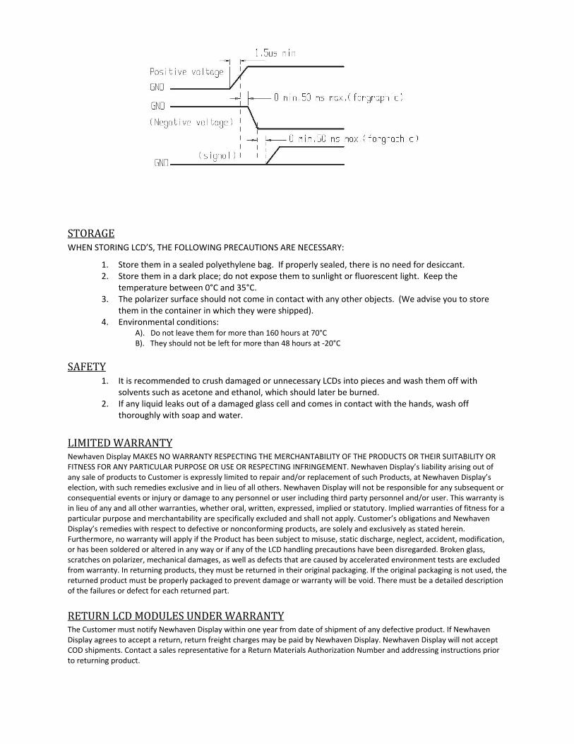
STORAGE WHEN STORING LCD’S, THE FOLLOWING PRECAUTIONS ARE NECESSARY:
1. Store them in a sealed polyethylene bag. If properly sealed, there is no need for desiccant. 2. Store them in a dark place; do not expose them to sunlight or fluorescent light. Keep the
temperature between 0°C and 35°C. 3. The polarizer surface should not come in contact with any other objects. (We advise you to store
them in the container in which they were shipped). 4. Environmental conditions:
A). Do not leave them for more than 160 hours at 70°C B). They should not be left for more than 48 hours at ‐20°C
SAFETY
1. It is recommended to crush damaged or unnecessary LCDs into pieces and wash them off with solvents such as acetone and ethanol, which should later be burned.
2. If any liquid leaks out of a damaged glass cell and comes in contact with the hands, wash off thoroughly with soap and water.
LIMITED WARRANTY Newhaven Display MAKES NO WARRANTY RESPECTING THE MERCHANTABILITY OF THE PRODUCTS OR THEIR SUITABILITY OR FITNESS FOR ANY PARTICULAR PURPOSE OR USE OR RESPECTING INFRINGEMENT. Newhaven Display’s liability arising out of any sale of products to Customer is expressly limited to repair and/or replacement of such Products, at Newhaven Display’s election, with such remedies exclusive and in lieu of all others. Newhaven Display will not be responsible for any subsequent or consequential events or injury or damage to any personnel or user including third party personnel and/or user. This warranty is in lieu of any and all other warranties, whether oral, written, expressed, implied or statutory. Implied warranties of fitness for a particular purpose and merchantability are specifically excluded and shall not apply. Customer’s obligations and Newhaven Display’s remedies with respect to defective or nonconforming products, are solely and exclusively as stated herein. Furthermore, no warranty will apply if the Product has been subject to misuse, static discharge, neglect, accident, modification, or has been soldered or altered in any way or if any of the LCD handling precautions have been disregarded. Broken glass, scratches on polarizer, mechanical damages, as well as defects that are caused by accelerated environment tests are excluded from warranty. In returning products, they must be returned in their original packaging. If the original packaging is not used, the returned product must be properly packaged to prevent damage or warranty will be void. There must be a detailed description of the failures or defect for each returned part.
RETURN LCD MODULES UNDER WARRANTY The Customer must notify Newhaven Display within one year from date of shipment of any defective product. If Newhaven Display agrees to accept a return, return freight charges may be paid by Newhaven Display. Newhaven Display will not accept COD shipments. Contact a sales representative for a Return Materials Authorization Number and addressing instructions prior to returning product.
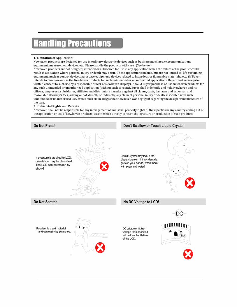
Handling Precautions
If pressure is applied to LCD,orientation may be disturbed.The LCD can be broken by shock!
Liquid Crystal may leak if thedisplay breaks. If it accidentallygets on your hands, wash them with soap and water!
Do Not Press! Don’t Swallow or Touch Liquid Crystal!
Do Not Scratch! No DC Voltage to LCD!
Polarizer is a soft material and can easily be scratched.
DC
No!
DC voltage or higher voltage than specifiedwill reduce the lifetimeof the LCD.
1. Limitation of Application:Newhaven products are designed for use in ordinary electronic devices such as business machines, telecommunications equipment, measurement devices..etc. Please handle the products with care. (See below)Newhaven products are not designed, intended or authorized for use in any application which the failure of the product could result in a situation where personal injury or death may occur. These applications include, but are not limited to: life-sustaining equipment, nuclear control devices, aerospace equipment, devices related to hazardous or lammable materials...etc. (If Buyer intends to purchase or use the Newhaven products for such unintended or unauthorized applications, Buyer must secure prior written consent to such use by a responsible oficer of Newhaven Display). Should Buyer purchase or use Newhaven products for any such unintended or unauthorized application (without such consent), Buyer shall indemnify and hold Newhaven and its oficers, employees, subsidaries, afiliates and distributors harmless against all claims, costs, damages and expenses, and reasonable attorney’s fees, arising out of, directly or indirectly, any claim of personal injury or death associated with such unintended or unauthorized use, even if such claim alleges that Newhaven was negligent regarding the design or manufacture of the part. 2. Industrial Rights and Patents Newhaven shall not be responsible for any infringement of industrial property rights of third parties in any country arising out of the application or use of Newhaven products, except which directly concern the structure or production of such products.

be reshaped, which willconductive rubber may
LCD may be shifted or
cause defects.
Pressure on the metallic frame and PCB may deformthe conductive rubber or break the liquid crystalcell and backlight, whichwill cause defects.
Do Not Put Pressure on the Metallic Frame or Disassemble the LCD Module
Avoid static electricity.
Slowly Peel Off Protective Film!
Please be sure to groundhuman body and electricappliances during work.
It is preferable to use aconductive mat on the tableand wear cotton clothesor conduction processedfiber. Synthetic fiber isnot recommended.
Avoid Static Electricity! Wear Gloves While Handing!
LCD deteriorates.
Keep Away From Extreme Heat and Humidity!
When attaching with theheat seal or anisotropicallyconductive film, wipe offwith alcohol before use.
Alcohol
Use Alcohol to Clean Terminals!
GLOVE
It is preferable to wear glovesto avoid damaging the LCD.
Please do not touch electrodeswith bare hands or leaveany residue.

Don’t Drop Water on LCD!
Precaution in Soldering LCD Module
Basic instructions: Solder I/O terminals only.Use soldering iron without leakage.(1)Soldering condition to I/O terminals
Temperature at tip of the iron: 280±10Soldering time: 3~4 sec.Type of solder: Eutectic solder (containing colophony-flux)*Do not use flux because it may soak into the LCD Module or contaminate it.*It is preferable to peel off protective film on the display surface after soldering I/Oterminals are complete.
(2)Remove connector or cable*When you remove connector or cable soldered to I/O terminals, please confirm that solder is fully melted. If you remove by force, electrodes at I/O terminals maybe damaged(or stripped off).*It is recommended to use a solder suction machine.
Long-term Storage
If it is necessary to store LCD modules for a period of time, please comply with thefollowing procedures.If storage conditions are not satisfactory, the display(especially polarizer)or soldering I/O terminals may become difficult(some oxide is generated at I/Oterminals plating).1.Store as delivered by Newhaven.2.If you store it unpacked, put it in an anti-static bag, seal its opening and store where it isnot subjected to direct sunlight or fluorescent light.
3.Store at temperature 0 to +35 and at low humidity.Please refer to our specificationsheets for storage temperature range and humidity conditions.
Long-term StoragePlease use power supply with built-in surge protection circuit.
Note that the presence ofwaterdrops or dew in the LCD panel may deterioratethe polarizer or corrodethe electrodes.