nh – 67, karur – trichy highways, puliyur c.f, 639 114 karur...
TRANSCRIPT
NH – 67, Karur – Trichy Highways, Puliyur C.F, 639 114 Karur District
DEPARTMENT OF ELETRONICS AND COMMUNICATION ENGINEERING
COURSE NOTES
SUBJECT: DIGITAL ELECTRONICS SUBJECT CODE: EC2203
FACULTY NAME/DESIGNATION: SUGAPRIYAA.THA / LECTURER
CLASS: II YEAR ECE
UNIT-II
COMBINATIONAL CIRCUITS
Design procedure – Half adder – Full Adder – Half subtractor – Full subtractor – Parallel binary adder,
parallel binary Subtractor – Fast Adder - Carry Look Ahead adder – Serial Adder/Subtractor - BCD adder
– Binary Multiplier – Binary Divider - Multiplexer/ Demultiplexer – decoder - encoder – parity checker –
parity generators – code converters - Magnitude Comparator.
OBJECTIVE
• To learn about the combinational circuits and to know about the analysis of those circuits
• To study about the design procedure of the combinational circuits
• Using the design procedure the code converters have to be designed
• Then standard combinational circuits like adders, subtractors, comparators, decoders,
encoders and multiplexers are introduced
Keywords: Combinational Circuits, Adders, Subtractor, Multiplier, Divider, Encoder, Decoder

COMBINATIONAL CIRCUITS
� Logic circuits are either combinational or sequential.
� Combinational logic circuits consists of logic gates whose outputs at any time are
determined from the present combination of the inputs.
� Sequential circuits consist of memory elements and logic gates.
ANALYSIS PROCEDURE
1. Obtain Boolean expression from logic diagram
a. Label all gate outputs that are a function of input variables. Obtain Boolean function for each
gate.
b. Label all gate outputs that are a function of input variables and previously labeled gates.
Obtain Boolean function for each of these gates.
c. Repeat step (b) until the outputs of the circuit are obtained.
2. Obtain the truth table from the logic diagram
a. Prepare the truth table for n input variables and 2n input combinations.
b. Label all gate outputs that are a function of input variables. Fill in the truth table for these
outputs.
c. Label all gate outputs that are functions of input variables and previously labeled gates. Fill in
the truth table columns for these outputs.
d. Repeat step (c) until the columns for all the outputs are obtained.
Example 1: Determine the Boolean functions for the outputs F and G as a function of the four
inputs A, B, C, and D.

Example 2: Analyze the previous logic circuit by establishing the truth table for F and G.

DESIGN PROCEDURE
1. Describe the problem (i.e., the problem statement).
2. Determine the available number of input variables and required output variables.
3. Assign letter symbols to the input and output variables.
4. Derive the truth table that defines the required relationships between inputs and outputs.
5. Obtain the simplified Boolean function for each output.
6. Draw the logic diagram.
Design of a Code Converter
Design a combinational logic circuit that will convert from a BCD code to Excess-3 code.
Design � 4 inputs � A, B, C, and C 4 outputs � w, x, y, and z
Truth Table:
The six unused combinations are considered don’t care conditions. These correspond to 10, 11,
12, 13, 14, and 15. Simplification of the output functions is made using Karnaugh maps and
making use of the don’t care conditions.
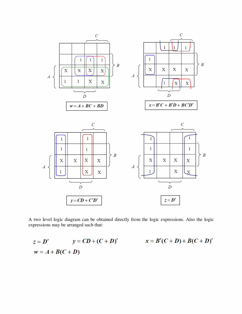
A two level logic diagram can be obtained directly from the logic expressions. Also the logic
expressions may be arranged such that:

Logic diagram for BCD to Excess-3 conversion
HALF ADDER
� Adding two single-bit binary values X, Y produces a sum S bit and a carry out C-out bit.
� This operation is called half addition and the circuit to realize it is called a half adder.
Truth Table
X Y SUM CARRY
0 0 0 0
0 1 1 0
1 0 1 0
1 1 0 1
Symbol
Figure. Half adder

S (X,Y) = (1,2)
S = X'Y + XY'
S = XY
CARRY(X,Y) = (3)
CARRY = XY
Circuit
FULL ADDER
� Full adder takes a three-bits input.
� Adding two single-bit binary values X, Y with a carry input bit C-in produces a sum bit S
and a carry out C-out bit.
Truth Table
X Y Z SUM CARRY
0 0 0 0 0
0 0 1 1 0
0 1 0 1 0
0 1 1 0 1
1 0 0 1 0
1 0 1 0 1
1 1 0 0 1
1 1 1 1 1
SUM (X,Y,Z) = (1,2,4,7)
CARRY (X,Y,Z) = (3,5,6,7)

Kmap-SUM
SUM = X'Y'Z + XY'Z' + X'YZ'
SUM = X ⊕ Y ⊕ Z
Kmap-CARRY
CARRY = XY + XZ + YZ
4-Bit Binary Adder

ADDITION OF TWO 4-BIT BINARY NUMBERS
The table shows the role of carry-in and carry-out.
4-bit binary parallel adder can be implemented in integrated circuit form by cascading 4 full
adders as shown below.
Disadvantage
� Slowing down of the addition due to the carry propagation time.

4-BIT PARALLEL ADDER/SUBTRACTOR
The 4-bit parallel adder can be modified to work as 4-bit parallel adder/subtractor by including 4
exclusive-OR gates to provide the 1's complement of B and adding 1 from the M input to make it
the 2's complement.
CARRY PROPAGATION AND THE LOOK-AHEAD CARRY CIRCUIT
� The carry propagate (Pi) and carry generate (Gi) variables are shown on the full adder
logic circuit.
� The carries C1, C2, and C3 can be expressed in SOP form as functions of C0 and the
different (Pi) and (Gi) as follows:

Therefore:
Similarly
The logic diagram of the look-ahead generator is implemented in a two level form as shown in
the following logic circuit.

The 4-Bit adder with the carry look-ahead circuit is implemented as shown in the following
circuit.
OVERFLOW
Overflow is defined as the situation when two N-digit numbers are added and the sum occupies
(N+1) digits. This situation occurs hen adding binary numbers as follows:
1. An end carry is generated when adding two N-bit unsigned
numbers.
2. The carry-in and carry-out bits are different when adding two N-bit signed binary
numbers.

DECIMAL ADDER
� Decimal numbers are presented in coded form in all case of digital devices for
manipulation.
� Accepting numbers in coded form and presenting the result in same form.
BCD ADDER
� One example of the decimal adder is BCD adder.
� It is useful because many digital devices process + display numbers in tens in BCD each
number is defined by a binary code of 4 bits.
� In order to add two decimal digits with a possible carry in of one, then the maximum sum
is 19. The following table shows the sum when performed in binary and compared to the
sum when performed in BCD. In both cases five outputs are needed.

� Inspecting the table reveals that a correction in the sum is needed when the sum is greater
than 9. The correction is adding 6 to the sum. The BCD adder will then consist of the 4-
bit binary adder.
� A second 4-bit binary adder is needed to add 6 to the sum when it is greater than 9. The
required logic circuit needed to detect if correction is needed can be obtained by
inspecting the table.
� A second method is to find a simplified expression for the carry out C of the five
variables K, Z8, Z4, Z2, and Z1. Minterms m20 to m31 are considered don’t care
conditions.
The logic circuit will be as follows

MAGNITUDE COMPARATOR
� To compare two 4-bit numbers (A3 A2 A1 A0) and (B3 B2 B1 B0), we have to design a
circuit with eight inputs and three outputs. The outputs are:
• A = B
• A > B
• A < B
� A better method to design this circuit is to follow the systematic way of comparison,
where we compare each pair of bits starting from the most significant bit.
� If all pairs are equal then A=B. If we find a difference in the compared bits (i.e. one is 1
and the other is 0), then the number containing the 1 is larger.
� This leads to the following three Boolean functions,

BINARY MULTIPLIER
To multiply two 2-bit binary numbers B1 B0 and A1 A0, we may use half adders and AND
gates.

BINARY DIVIDER
� The binary divisions are performed in a very similar manner to the decimal divisions, as
shown in the below figure examples.
� Thus, the second number is repeatedly subtracted from the figures of the first number
after being multiplied either with '1' or with '0'.
� The multiplication bit ('1' or '0') is selected for each subtraction step in such a manner that
the subtraction result is not negative.
� The division result is composed from all the successive multiplication bits while the
remainder is the result of the last subtraction step.
� This algorithm can be implemented by a series of subtracters composed of modified
elementary cells.
� Each subtracter calculates the difference between two input numbers, but if the result is
negative the operation is canceled and replaced with a subtraction by zero.
� Thus, each divider cell has the normal inputs of a subtracter unit as in the figure below
but a supplementary input ('div_bit') is also present.
� This input is connected to the b_req_out signal generated by the most significant cell of
the subtracter. If this signal is '1', the initial subtraction result is negative and it has to be
replaced with a subtraction by zero.
� Inside each divider cell the div_bit signal controls an equivalent 2:1 multiplexer that
selects between bit 'x' and the bit included in the subtraction result X-Y.
� The complete division can therefore by implemented by a matrix of divider cells
connected on rows and columns as shown in figure below.
� Each row performs one multiplication-and-subtraction cycle where the multiplication bit
is supplied by the NOT logic gate at the end of each row.
� Therefor the NOT logic gates generate the bits of the division result.

MULTIPLEXERS
� A multiplexer is a combinational circuit that selects one of many input lines ( normally 2n
lines) and directs it to a single output line.
� The selection of a particular input line is controlled by a set of election lines ( normally n
selection lines).
2-to-1 Line Multiplexer
A 2-to-1 line multiplexer has two inputs, one selection line and one output. This is shown in the
following logic circuit.
4-to-1 Line Multiplexer
� A 4-to-1 line multiplexer consists of four AND gates. Each input is connected to one
AND gate.

� Selection lines S1 and S0 are decoded to select a particular AND gate.
� The outputs of the AND gates are applied to a single OR gate that provides the output of
the multiplexer Y.
� The output of the multiplexer is then given by:
The function table of the multiplexer is shown next.
S1 S
0 Y
0 O I0
0 1 I1
1 0 I2
1 1 I3
Multiplexers may have an enable input, similar to decoders, to control the operation of the unit.
A quadruple 2-to-1 multiplexer with enable input is shown next.

The function table of the quadruple 2-to-1 multiplexer with the enable input will be as follows:
E S Y
1 X All 0’s
0 0 Select A
0 1 Select B
BOOLEAN FUNCTION IMPLEMENTATION
� A multiplexer is a decoder and an OR gate that provides the output.
� The multiplexer can be used to implement Boolean functions of n variables.
� This can be achieved using either 2n-to-1 multiplexer or 2(n-1)-to-1 multiplexer.
� Using 2n-to-1 multiplexer The n variables are connected to the n selection lines.
� Each input of the multiplexer is set to 0 or 1, depending on which minterm of the function
is present.

DECODERS
� A binary code of n bits is capable of representing up to 2n
distinct elements of coded
information.
� A decoder is a combinational circuit that converts binary information from n input lines
to up to 2n
output lines.
� These decoders are called n-to-m line decoders such that:
m ≤ 2n
3-to-8 Line Decoder
� A 3-to-8 line decoder has three elements and eight outputs.
� The decoder decodes the input binary code represented by the three bits and generates all
eight minterms of the inputs.
� Only one utput is one while the other seven are zeros.
� This decoder can be implemented using three inverters and eight AND gates as shown.
3-to-8 Line Decoder

The following truth table is for the decoder.
2-to-4 Line Decoder with Enable Input Using NAND gates
If we use NAND gates to construct the decoder then the outputs are inverted. Decoders are also
constructed with one or more enable inputs. An example is shown for the 2-to4 line decoder.

DEMULTIPLEXERS
� A decoder with enable input can function as a demultiplexer.
� A demultiplexer is a combinational circuit that has one input and up to 2n outputs and it
directs the input to an output depending on the values of n selection lines.
A 4 X 16 decoder can be constructed from two 3 X 8 decoders with enable inputs.
ENCODERS
� An encoder is a digital circuit that performs the inverse operation of the decoder.
� It has 2n inputs and n outputs that represents the code of the order of the input that is set
to one.
The truth table of an octal to binary encoder is shown below.

The encoder is implements by OR gates. As given in the truth table, the outputs are given by:
This encoder has two main drawbacks:
1. When more than one input is 1 at the same time, then the output could indicate a wrong
code. E.g. D5 and D6 are one at the same time, then x,y, and z are ones indicating D7 is
one.
2. If no input is one, which is not valid code, then the outputs are all zeros, which indicates
a code for D0.
To overcome these problems, we may use a priority encoder.
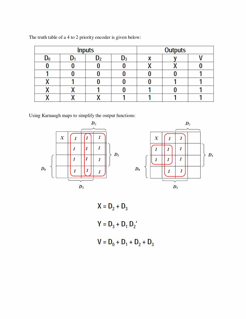
The truth table of a 4 to 2 priority encoder is given below:
Using Karnaugh maps to simplify the output functions:

CODE CONVERSION
� Code conversion is necessary to achieve the compatibility between two different systems
following different coding schemes.
� The code that has to be converted is applied as the inputs and the output gives the
transferred code. BCD to Excess-3 conversion was given already.
EXCESS-3 TO BCD CODE CONVERSION
The truth table for excess-3 to BCD is constructed and from the table the equation for conversion
of BCD to excess-3 is obtained. It is then implemented with the help of logic gates.
Truth Table

By applying K-map method the simplified circuit is shown below
Excess-3 to BCD converter

BINARY TO GRAY CODE CONVERTER
� The first bit of the gray code will be the same as the first bit of the binary code.
� Second bit of gray code is obtained by the XOR operation of first two bits in the binary
code.
� Similarly third bit is obtained by the XOR combination of second and third bit in binary
and so on.
Truth Table
Binary to Gray converter

GRAY TO BINARY CODE CONVERTER
Truth Table
Gray to Binary converter
PARITY CHECKING AND GENERATION
� It is the simple error detecting code by appending or prepending one (parity) bit in each
data word at the transmitter.
� The bit added will make the total number of 1s in the word (including parity bit) as even
or odd.
� The receiver detects the error by counting the number of 1s in each word.
� IC 74180 is used to check/generate even/odd parity of the 9-bit data.
PIN configuration
� The data (X0 – X7) along with the Even or odd input (9-bits in total) is checked by the
IC.
� It will act as the parity generator if PE = 1, PO = 0 (shown in first two entry in truth
table).
� These inputs also taken into account while counting for the 1s. ∑ even output will glow
to generate a 1 to make the total number of 1s even.

7404
1 2
>EVENO/P
ODDO/P
>
330k
>
E EVEN
>
LED
>
EVEN
330k
>
>
IC 74180
MODE
>
X11 E ODD
> LED
IC 74180
ODD
>
X6
X0
X14
>
X15
X1
X12
>
X8
X2
X7 >
X3
> X4
X13
ODD
EVEN
>>
X9
X5
X10 >
>
� The last two entries show the IC operation as parity checker. It checks the number of 1s
in those 9-bits and gives output accordingly.
� Both the ∑ outputs are produced simultaneously. Output is derived from any of these
two pins depending up on the parity we follow.
TRUTH TABLE
� IC 74180 is cascaded to increase the word length capability from 9-bit to 16-bit.
� It is shown below. MODE = 1 for checking parity and for MODE = 0, for generating
parity.
Bit parity checker/Generator

SUMMARY
Combinational logic: The combinational circuit consists of logic gates whose output is
determined by present combination of inputs.
Design procedure:
1. Describe the problem (i.e., the problem statement).
2. Determine the available number of input variables and required output variables.
3. Assign letter symbols to the input and output variables.
4. Derive the truth table that defines the required relationships between inputs and outputs.
5. Obtain the simplified Boolean function for each output.
6. Draw the logic diagram.
Half-Adder
Half adder is a combinational circuit that performs the addition of two bits.
Full-Adder It is a combinational circuit that performs the addition of three bits.
Binary-Adder
A binary adder is a digital circuit that produces the arithmetic sum of two binary numbers
Decimal Adder Decimal numbers are presented in coded form in all case of digital devices for manipulation.
Multiplexers
A multiplexer is a combinational circuit that selects one of many input lines ( normally 2n
lines)
and directs it to a single output line.
Decoders
A decoder is a combinational circuit that converts binary information from n input lines to up to
2n
output lines
Encoders
An encoder is a digital circuit that performs the inverse operation of the decoder.
Code Conversion
Code conversion is necessary to achieve the compatibility between two different systems
following different coding schemes.

Parity Checking And Generation
It is the simple error detecting code by appending or prepending one (parity) bit in each data
word at the transmitter. The bit added will make the total number of 1s in the word (including
parity bit) as even or odd.
Review Questions
2-marks
1. Define combinational logic
2. Explain the design procedure for combinational circuits
3. Define Half adder and full adder
4. What do you mean by carry look ahead adder?
5. Define Decoder
6. What is binary decoder?
7. Define Encoder?
8. What is priority Encoder?
9. Define multiplexer?
10. What do you mean by comparator?
11. Which gate is equal to AND-invert Gate?
12. Which gate is equal to OR-invert Gate?
Big Questions
1. Implement F(x,y,z) = Σ(1,2,6,7) using 8-to-1 multiplexer.
2. Implement F(x,y,z) = Σ(1,2,6,7) using 4-to-1 multiplexer.
3. Implement a full adder circuit using an appropriate decoder and OR gates.
4. Design a 4 bit magnitude comparator to compare two 4 bit number
5. Construct a combinational circuit to convert given binary coded decimal number into an
Excess 3 code for example when the input to the gate is 0110 then the circuit should
generate output as 1001
6. Design a combinational logic circuit whose outputs are F1 = a’bc + ab’c and
F2 = a’ + b’c + bc’
7.
(a) Draw the logic diagram of a *-bit 7483 adder
(b) Using a single 7483, Draw the logic diagram of a 4 bit adder/sub tractor
8. Realize a BCD to Excess 3 code conversion circuit starting from its truth table
(a) Design a full sub tractor
(b) How to it differ from a full sub tractor
9. Design a combinational circuit which accepts 3 bit binary number and converts its
equivalent excess 3 codes
10. Derive the simplest possible expression for driving segment “a” through ‘g’ in an 8421
BCD to seven segment decoder for decimal digits 0 through 9 .Output should be active
high (Decimal 6 should be displayed as 6 and decimal 9 as 9)