next generation nanosatellite standard design …
TRANSCRIPT

1
NEXT GENERATION NANOSATELLITE STANDARD
DESIGN SPECIFICATION
Written by: Pol Via
Revised by: Adriano Camps
Barcelona, February 2017
2
Table of contents
Table of contents .............................................................................................................. 2
List of Figures ................................................................................................................... 4
List of Tables .................................................................................................................... 5
Glossary ........................................................................................................................... 6
1. The Next Generation: A Truly Modular Hardware Standard ....................................... 7
1.1. General Overview ............................................................................................... 7
1.1.1. Concept of Module and miniModule ............................................................ 7
1.1.2. Concept of Data Bus and Power Bus .......................................................... 8
1.1.3. Standardized Interfaces and Power Supply Voltages .................................. 9
1.1.3.1. Interfaces for Subsystem-to-Subsystem communication ........................... 9
1.1.3.2. Interfaces for Subsystem-to-Payload communication .............................. 10
1.1.3.3. Power supply rails ................................................................................... 10
1.2. The Next Generation Standard Design Specification ........................................ 11
2. Next Generation Standard Design Specification ...................................................... 12
2.1. Module Form Factor ......................................................................................... 12
2.1.1. Programming/Debugging/Testing ports ..................................................... 13
2.1.2. miniModules Form Factor .......................................................................... 13
2.1.3. Parent Module Form Factor ....................................................................... 14
2.2. Data Bus .......................................................................................................... 15
2.2.1. Connector .................................................................................................. 15
2.2.2. Pin Assignment ......................................................................................... 16
2.2.3. miniData Bus ............................................................................................. 17
2.3. Power Bus ........................................................................................................ 19
2.3.1. Connector .................................................................................................. 19
2.3.2. Pin Assignment ......................................................................................... 19
2.3.3. miniPower Bus .......................................................................................... 20

3
2.4. Stacking Height Options ................................................................................... 20

4
List of Figures
Figure 1: Module form factor ........................................................................................... 12
Figure 2: Module Programming/Debugging/Testing ports ............................................... 13
Figure 3: miniModule form factor (bottom layer) .............................................................. 14
Figure 4: Parent Module with 2 slots for miniModules in the top layer ............................. 15
Figure 5: Rendered image of the connector used in the Data Bus .................................. 16
Figure 6: Detail of the miniData Bus connector (credit: Samtec) ..................................... 18
Figure 7: Detail of the connector used in the Power Bus (credit: Samtec) ....................... 19
Figure 8: Staking height options, A-F .............................................................................. 21
Figure 9: Stacking height options: G-H ........................................................................... 21

5
List of Tables
Table 1: S2S standardized interfaces ............................................................................... 9
Table 2: S2P standardized interfaces ............................................................................. 10
Table 3: Data Bus pin assignment .................................................................................. 16
Table 4: miniData Bus pin assignment ............................................................................ 18
Table 5: Power Bus pin assignment ................................................................................ 19
Table 6: miniPower Bus pin assignment ......................................................................... 20
Table 7: Stacking height options .................................................................................... 22

6
Glossary
CAN Controller Area Network
COTS Commercial off the Shelf
CSKB CubeSat Kit Bus
EPS Electrical Power System
GPIO General Purpose Input/Output
I2C Inter-Integrated Circuit
I/O Input/Output
MCU Microcontroller Unit
MPPT Maximum Power Point Tracker
OBC On-Board Computer
PCB Printed Circuit Board
RF Radiofrequency
S2P Subsystem-to-Payload
S2S Subsystem–to–Subsystem
SPI Serial Peripheral Interface
SMD Surface Mount Device
TBD To Be Determined
UART Universal Asynchronous Transmitter-Receiver
USART Universal Synchronous/Asynchronous Transmitter-Receiver
USB2.0 Universal Serial Bus 2.0
USB3.0 Universal Serial Bus 3.0

7
1. The Next Generation: A Truly Modular Hardware Standard
This standard, which has been presented in the AVT-257/RSM-041 “Best Practices for Risk
Reduction for Overall Space Systems” conference organized by NATO held in Zaragoza,
during September 2016, presents the guidelines for the development of new CubeSat
hardware in the NanoSat Lab. The goal of the standard is to guide the next generation of
CubeSat hardware to a new level of modularity and versatility and to improve the ease of
integration for products from different manufacturers/universities at a mechanical and
electrical level.
1.1. General Overview
As in the CSKB standard, the new standard is based on the same idea of stacking PCBs,
as opposed –for example- to a back plane approach, and electrically connect them via
stackable connectors for both the data and power buses. Nevertheless, the new standard
focuses on enabling improved modularity, versatility and a better performance in general.
The performance improvement comes from two basic reasons:
- The standardization of modern stackable connectors with high pin density
and differential pair signalling allowing space savings in the PCB due to reduced
size of the connector making possible the routing of modern interfaces which
take advantage of differential pair and improved signal integrity.
- The standardization of modern interfaces to interconnect all the subsystems
and payloads, in front of the more conventional used by the CSKB standard,
leads into a faster and more reliable communication which allows to fly payloads
with higher data rate requirements.
The new standard for the future CubeSat hardware development in the UPC defines:
- PCB form factor (PCB size and mounting holes)
- Data Bus and Power Bus connector type and position
- Stacking height options
- Interfaces for Subsystem-to-Subsystem and Subsystem-to-Payload
communication
- Power supply voltages
1.1.1. Concept of Module and miniModule
The concept of a Module: is very similar to the concept of a subsystem. In CubeSats it is
common to dedicate a PCB inside the satellite to every subsystem, to then stack and
interconnect them through board-to-board connectors. The concept of stacking boards is
inherited from the widely popular industry standard PC104 ¡Error! No se encuentra el
origen de la referencia., an embedded computer standard that defines both the form
factor of the PCBs, and the system data and power buses. Many universities decided to
develop their first subsystems in compliance with the PC104 board form factor, and the
same data bus connector that allows PCB stacking, but modifying the pin assignment.
Some companies have kept basing their platforms on the PC104, but while the PC104
standard has evolved to modern connectors with higher pin density and enhanced signal
integrity, most companies are still using simpler connector definitions introduced in the
initial releases of the PC104. This is commonly known as the CubeSat Kit Bus standard.

8
The proposal presented in this project applies the same module stacking philosophy where
each module is mapped to a satellite/spacecraft subsystem. Usually, modules consist of a
single PCB, although larger subsystems (e.g. Reaction Wheels) tend to integrate a set of
PCBs and mechanical parts, but keeping the same data and power buses definition. The
size of the modules and their attachment to the structure is standardized as well as the
data and power bus connectors. Unlike the current trend, it is proposed the use of high
density pin connectors with improved signal integrity, and optimized differential pair
signalling. Other ports and connectors including programming/debugging ports are also
standardized in terms of connector type and position inside the module.
The concept of a miniModule (or daughterboard): is a simple idea that tries to ease the
integration and maximize the available space for the payload inside the satellite. Smaller
subsystems that do not need an entire PCB (module) can be implemented in smaller PCBs
called miniModules, that are later mounted in slots located at parent modules specifically
designed to allocate one or more miniModules. The connection between the miniModule
and the parent module is performed by a reduced version of the data and power buses
based on two board-to-board connectors (one for the data and another for the power) that
wire the most important interfaces, and power rails to the miniModules. Within the proposed
approach a module could host up to four miniModules (see Appendix A).
1.1.2. Concept of Data Bus and Power Bus
The Data bus: is a set of organized interfaces that aim at interfacing all the subsystems
within a satellite. Physically, the Data Bus is a bus that crosses the satellite carrying all the
signals through the stackable connector that, as mentioned before, must be capable of
carrying differential pair signalling.
The proposed Data Bus aims at minimizing the number of interfaces used to communicate
the subsystems, as well as to minimizel the protocols to be standardized and maximize the
interfaces available for communication with the payload. In order to communicate all the
subsystems, the CAN (Controller Area Network) ¡Error! No se encuentra el origen de la
referencia. and I2C (Inter-Integrated Circuit) ¡Error! No se encuentra el origen de la
referencia. are proposed together with SPI ¡Error! No se encuentra el origen de la
referencia. (Serial Peripheral Interface) for those data transfers requiring bit rates higher
than 1 Mbps (CAN bit rate limit is 1 Mbps) having always in mind that the maximum speed
for the SPI is directly related to the signal integrity conditions. The Data Bus also includes
Ethernet ¡Error! No se encuentra el origen de la referencia., USB3.0 ¡Error! No se
encuentra el origen de la referencia., USB2.0 ¡Error! No se encuentra el origen de la
referencia., UART/USART. Ethernet’s typical applications are payloads that generate
large amounts of data (e.g. high resolution cameras); USB’s typical applications are COTS
(Commercial Off The Shelf) component based payloads (e.g. Software Defined Radios)
and UART or USART are typically used for simpler payloads managed by microcontrollers.
There is also a reduced Data Bus called miniData Bus which electrically connects one or
more miniModules with its parent module, but only a fraction of the interfaces available in
the satellite’s Data Bus are routed into the miniModules via the miniData Bus.

9
The Power Bus: The Power Bus is a set of organized power rails which supply electrical
power to all the subsystems within a satellite. The Power Bus is physically similar to the
Data Bus and also consists on a bus crossing through the satellite and it is also based on
a stackable connector. The Power Bus distributes the power from the Electrical Power
Subsystem (EPS) to the different subsystems and payloads. The voltages levels available
at the Power Bus are standardized.
There is also a reduced Power Bus called miniPower Bus which electrically connects one
or more miniModules with its parent module but only a fraction of the supply rails available
in the satellite’s Power Bus are routed into the miniModules via the miniPower Bus.
1.1.3. Standardized Interfaces and Power Supply Voltages
The interfaces and power supply lines which travel through the satellite’s Data Bus and
Power Bus are standardized as well as the connectors pin assignment.
1.1.3.1. Interfaces for Subsystem-to-Subsystem communication
The Subsystem-to-Subsystem (S2S) communications are intended to carry information
between two or more subsystems. Those communications hardly never require a high data
rate as they are normally commands, status messages or sensor readings. The only
exception is the communication between the OBC and the Communication Subsystem
during downlink operations when large files containing information about the satellite’s
status and scientific data from the payload are being transmitted to the Earth.
For those reasons, the standardized interfaces for S2S communication are:
Table 1: S2S standardized interfaces
CAN I2C SPI
Data rate Up to 1 Mbps, high
speed
100 kbps, standard
mode, low speed
Very High, depends
on signal integrity
Signal Integrity Strong, interference
immunity
Weak, interference
sensitive
Weak, interference
sensitive
Data error
correction
Yes No No
Topology Bus, allows system
expandability
Bus (master-slave),
allows system
expandability
Bus (master-slave),
limited system
expandability
Power
Consumption
High Low Low
The CAN bus is chosen for its high data rate, strong signal integrity of its physical layer,
and because it allows system expandability as more devices can be added to the bus in
any moment. Because CAN is a very complex bus and requires a lot of power, I2C is also
standardized as an alternative. SPI is also standardized, but should be avoided and is only
recommended to use for high speed applications. Also USB2.0 or USB3.0 can be used in
the case that one or more subsystems are based on commercial devices which only have
this port available.

10
1.1.3.2. Interfaces for Subsystem-to-Payload communication
The Subsystem-to-Payload (S2P) communications are intended to carry information
between a subsystem (normally the OBC) and a payload. Those communications can
sometimes require a high speed link specially in case of imaging payloads.
For those reasons. The standardized interfaces for S2P communication, aside from SPI,
I2C, and CAN are:
Table 2: S2P standardized interfaces
UART/USART USB2.0/3.0 10/100/1000
Ethernet
Data rate 100 kbps, low speed Very high, (2.0 –
480 Mbps, 3.0 - 4.8
Gbps)
Up to 1 Gbps
Signal Integrity Strong Extremely sensitive
to interference
Sensitive to
interference
Topology Point-to-point Point-to-point Point-to-point
Power
Consumption
Low High High
For S2P communications a large number of interfaces are standardized to offer the
maximum of versatility and enable the usage of commercial and industrial grade based
payloads.
Note: Due to the high complexity of implementing a physical layer driver in a PCB for the
USB2.0/3.0 and the Ethernet (1000base-T implementation) interfaces, the complexity of
maintaining proper signal integrity conditions and the difficulty of physically debugging and
testing the physical layer it is likely that those interfaces are not included in the next release
of the standard.
1.1.3.3. Power supply rails
The power supply rails are in charge of the transporting the electricity from the Electrical
Power System (EPS) to each subsystem or payload. The EPS, commanded from the On-
Board Computer (OBC) turns on and off each rail as well as it monitors the voltage and
current passing through them.
The standardized voltages for the power supply rails are:
- 12V: intended for high power consumption payloads and subsystems (example:
downlink communications or attitude control)
- 5V: intended for medium power consumption payloads and subsystems
- 3,3V: intended for low power consumption subsystems (example: EPS, OBC).
The connectors and PCB tracks that carry those rails must be designed to withstand a
maximum of 3 A through each rail. Parameters that define the quality and stability of the
supply rails, such as the ripple, voltage drops, Vrms …, are yet TBD.
11
1.2. The Next Generation Standard Design Specification
The first version of the design specification document of the Next Generation Standard can
be found on the Annex A (2).

12
2. Next Generation Standard Design Specification
2.1. Module Form Factor
- The Modules are 90 mm by 90 mm PCBs
- The Modules shall have four 3.5 mm diameter mounting holes located 5 mm
from the edges of the board
- The Modules shall have a Data Bus connector on the top layer and another on
the bottom layer
- The Modules shall have a Power Bus connector on the top layer and another
on the bottom layer
- The Data Bus and Power Bus positions are TBD
Figure 1: Module form factor

13
2.1.1. Programming/Debugging/Testing ports
- The MCU or other devices programming ports shall be located within a specific
area in the top layer and must be right angle connectors
- The MCU or other devices debugging ports shall be located within a specific
area in the top layer and must be right angle connectors
- The MCU or other devices testing ports shall be located within a specific area
in the top layer and must be right angle connectors
- The headers with the plugged housings must not overhang the edge of the
board.
Figure 2: Module Programming/Debugging/Testing ports
2.1.2. miniModules Form Factor
- The miniModules are 60 mm by 40 mm PCBs
- The miniModules shall have four 2.4 mm diameter mounting holes located 2.5
mm from the edges of the board
- The miniModules shall have a male miniData Bus connector on the bottom layer
- The miniModules shall have a male miniPower Bus connector on the bottom
layer
- The miniData Bus and miniPower Bus positions are TBD

14
Figure 3: miniModule form factor (bottom layer)
2.1.3. Parent Module Form Factor
A parent Module is a special Module that can host up to 4 miniModules
- Parent Modules shall comply with the Module Form Factor rules
- Parent Modules shall, at least, be able to host one miniModule
- Parent Modules shall not host more than four miniModules (two on the top layer
and two on the bottom layer
- Parent Modules shall not host more than two modules in the same layer
- Parent Modules shall contain the mounting holes for each miniModule it can
host
- Parent Modules shall have a miniData Bus connector for each miniModule they
can host
- Parent Modules shall have a miniPower Bus connector for each miniModule
they can host

15
Figure 4: Parent Module with 2 slots for miniModules in the top layer
2.2. Data Bus
2.2.1. Connector
The Data Bus connector is based on the SAMTEC LSHM connectors, a SMD, stackable
high density pin, hermaphrodite (does not need a male and a female version) series of
connectors with high reliability, metal shielding and multiple stacking height options.
Connector part number: LSHM-150-0X.0-L-DV-A-S (where X = 3, 4, 6 defines the
connector height).

16
Figure 5: Rendered image of the connector used in the Data Bus
2.2.2. Pin Assignment
Table 3: Data Bus pin assignment
Data Bus Pin Assignment
Pin # Function Function Pin #
1 SHIELD SHIELD 2
3 ETHERNET 0 (D1+) ETHERNET 1 (D1+) 4
5 ETHERNET 0 (D1-) ETHERNET 1 (D1-) 6
7 SHIELD SHIELD 8
9 ETHERNET 0 (D2+) ETHERNET 1 (D2+) 10
11 ETHERNET 0 (D2-) ETHERNET 1 (D2-) 12
13 SHIELD SHIELD 14
15 ETHERNET 0 (D3+) ETHERNET 1 (D3+) 16
17 ETHERNET 0 (D3-) ETHERNET 1 (D3-) 18
19 SHIELD SHIELD 20
21 ETHERNET 0 (D1+) ETHERNET 1 (D1+) 22
23 ETHERNET 0 (D1-) ETHERNET 1 (D1-) 24
25 SHIELD SHIELD 26
27 USB3.0 (D+) USB2.0 (D+) 28
29 USB3.0 (D-) USB2.0 (D-) 30
31 SHIELD SHIELD 32
33 USB3.0 (VUSB) USB2.0 (VUSB) 34
35 SHIELD SHIELD 36
37 USB3.0 (SSRX+) USB3.0 (SSTX+) 38
39 USB3.0 (SSRX-) USB3.0 (SSTX-) 40
41 SHIELD SHIELD 42
43 CAN 0 (H) CAN 1 (H) 44
45 CAN 0 (L) CAN 1 (L) 46
47 SHIELD SHIELD 48
49 I2C 0 (SCL) I2C 1 (SCL) 50

17
51 I2C 0 (SDA) I2C 1 (SDA) 52
53 SHIELD SHIELD 54
55 USART 0 (RXD) USART 1 (RXD) 56
57 USART 0 (CTS) USART 1 (CTS) 58
59 USART 0 (TXD) USART 1 (TXD) 60
61 USART 0 (RTS) USART 1 (RTS) 62
63 USART 0 (SCK) USART 1 (SCK) 64
65 UART 0 (RXD) UART 1 (RXD) 66
67 UART 0 (TXD) UART 1 (TXD) 68
69 SHIELD SHIELD 70
71 SPI 0 (SCK) SPI 0 (SCK) 72
73 SPI 0 (MISO) SPI 0 (MISO) 74
75 SPI 0 (MOSI) SPI 0 (MOSI) 76
77 SPI 0 (CS0) SPI 0 (CS0) 78
79 SPI 0 (CS1) SPI 0 (CS1) 80
81 SHIELD SHIELD 82
83 GPIO0/A0 GPIO8/A4 84
85 GPIO1/A1 GPIO9/A5 86
87 GPIO2/A2 GPIO10/A6 88
89 GPIO3/A3 GPIO11/A7 90
91 GPIO4/PWM0_H GPIO12/PWM2_H 92
93 GPIO5/PWM0_L GPIO13/PWM2_L 94
95 GPIO6/PWM1_H GPIO14/PWM3_H 96
97 GPIO7/PWM1_L GPIO15/PWM3_L 98
99 SHIELD SHIELD 100
Notes:
- The USB3.0 bus can be used as another USB2.0
- The USART buses can be used as UART
- Pins 83 to 98 are intended for general purpose and can be used as Analog I/O,
Digital I/O, PWM, general purpose differential pair, or MCU interruption pins
2.2.3. miniData Bus
The miniData Bus electrically connects one or more miniModules with its parent module.
The connector used is a SAMTEC SS5-30-3.50-L-D which provides high reliability and
differential pair optimization. The female connector is placed on the parent Module and the
female connector is placed on the miniModule.

18
Figure 6: Detail of the miniData Bus connector (credit: Samtec)
Only a fraction of the interfaces available in the satellite are routed into the miniModules
via the miniData Bus. The detailed pin assignment below shows what interfaces are
available to the miniModules.
Table 4: miniData Bus pin assignment
miniData Bus Pin Assignment
Pin
# Function Function
Pin
#
1 SHIELD SHIELD 2
3 GPIO0/A0 GPIO8/A4 4
5 GPIO1/A1 GPIO9/A5 6
7 GPIO2/A2 GPIO10/A6 8
9 GPIO3/A3 GPIO11/A7 10
11 GPIO4/PWM0_H GPIO12/PWM2_H 12
13 GPIO5/PWM0_L GPIO13/PWM2_L 14
15 GPIO6/PWM1_H GPIO14/PWM3_H 16
17 GPIO7/PWM1_L GPIO15/PWM3_L 18
19 USB3.0 (VUSB) USB2.0 (VUSB) 20
21 SHIELD SHIELD 22
23 USB3.0 (D+) USB2.0 (D+) 24
25 USB3.0 (D-) USB2.0 (D-) 26
27 SHIELD SHIELD 28
29 CAN 0 (H) CAN 1 (H) 30
31 CAN 0 (L) CAN 1 (L) 32
33 SHIELD SHIELD 34
35 I2C 0 (SCL) I2C 1 (SCL) 36
37 I2C 0 (SDA) I2C 1 (SDA) 38
39 USART 0 (RXD) USART 1 (RXD) 40
41 USART 0 (CTS) USART 1 (CTS) 42
43 USART 0 (TXD) USART 1 (TXD) 44
45 USART 0 (RTS) USART 1 (RTS) 46
47 USART 0 (SCK) USART 1 (SCK) 48
49 SPI 0 (SCK) SPI 0 (SCK) 50

19
51 SPI 0 (MISO) SPI 0 (MISO) 52
53 SPI 0 (MOSI) SPI 0 (MOSI) 54
55 SPI 0 (CS0) SPI 0 (CS0) 56
57 SPI 0 (CS1) SPI 0 (CS1) 58
59 SHIELD SHIELD 60
2.3. Power Bus
2.3.1. Connector
The Power Bus connector is based on the SAMTEC LSEM connectors, a SMD, stackable
hermaphrodite (does not need a male and a female version) series of connectors with high
reliability and multiple stacking height options.
Connector part number: LSEM-130-0Y.0-L-DV-A-N (where Y = 3, 4, 6 defines the
connector height).
Figure 7: Detail of the connector used in the Power Bus (credit: Samtec)
2.3.2. Pin Assignment
Table 5: Power Bus pin assignment
Power Bus Pin Assigment
Pin # Function Function Pin #
1 GND 12V Rail 1 2
3 GND 12V Rail 1 4
5 GND 12V Rail 2 6
7 GND 12V Rail 2 8
9 GND 12V Rail 3 10
11 GND 12V Rail 3 12
13 GND 12V Rail 4 14
15 GND 12V Rail 4 16
17 GND 12V Rail 5 18
19 GND 12V Rail 5 20
21 GND 5V Rail 1 22
23 GND 5V Rail 1 24
25 GND 5V Rail 2 26
20
27 GND 5V Rail 2 28
29 GND 5V Rail 3 30
31 GND 5V Rail 3 32
33 GND 5V Rail 4 34
35 GND 5V Rail 4 36
37 GND 5V Rail 5 38
39 GND 5V Rail 5 40
41 GND 3V3 Rail 1 42
43 GND 3V3 Rail 1 44
45 GND 3V3 Rail 2 46
47 GND 3V3 Rail 2 48
49 GND 3V3 Rail 3 50
51 GND 3V3 Rail 3 52
53 GND 3V3 Rail 4 54
55 GND 3V3 Rail 4 56
57 GND 3V3 Rail 5 58
59 GND 3V3 Rail 5 60
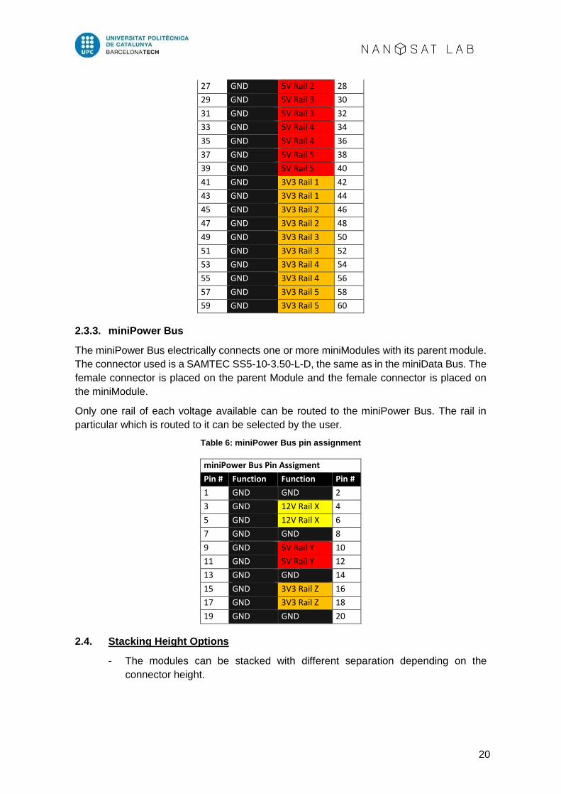
2.3.3. miniPower Bus
The miniPower Bus electrically connects one or more miniModules with its parent module.
The connector used is a SAMTEC SS5-10-3.50-L-D, the same as in the miniData Bus. The
female connector is placed on the parent Module and the female connector is placed on
the miniModule.
Only one rail of each voltage available can be routed to the miniPower Bus. The rail in
particular which is routed to it can be selected by the user.
Table 6: miniPower Bus pin assignment
miniPower Bus Pin Assigment
Pin # Function Function Pin #
1 GND GND 2
3 GND 12V Rail X 4
5 GND 12V Rail X 6
7 GND GND 8
9 GND 5V Rail Y 10
11 GND 5V Rail Y 12
13 GND GND 14
15 GND 3V3 Rail Z 16
17 GND 3V3 Rail Z 18
19 GND GND 20
2.4. Stacking Height Options
- The modules can be stacked with different separation depending on the
connector height.

21
Figure 8: Staking height options, A-F
Figure 9: Stacking height options: G-H

22
Table 7: Stacking height options