network electrophysiology sensor-on-a-chip by tsai-yuan chen a
TRANSCRIPT
Network Electrophysiology Sensor-On-A-Chip
by
Tsai-Yuan Chen
A ThesisSubmitted to the Faculty
of theWORCESTER POLYTECHNIC INSTITUTEin partial fulfillment of the requirements for the
Degree of Doctor of Philosophyin
Electrical and Computer Engineeringby
May 2011
APPROVED:
Professor John A. McNeill, Major Advisor
Professor Edward A. Clancy
Doctor Michael Coln

Abstract
Electroencephalogram (EEG), Electrocardiogram (ECG), and Electromyogram (EMG)
bio-potential signals are commonly recorded in clinical practice. Typically, patients are
connected to a bulky and mains-powered instrument, which reduces their mobility and
creates discomfort. This limits the acquisition time, prevents the continuous monitoring
of patients, and can affect the diagnosis of illness. Therefore, there is a great demand for
low-power, small-size, and ambulatory bio-potential signal acquisition systems.
Recent work on instrumentation amplifier design for bio-potential signals can be broadly
classified as using one or both of two popular techniques: In the first, an AC-coupled signal
path with a MOS-Bipolar pseudoresistor is used to obtain a low-frequency cutoff that passes
the signal of interest while rejecting large dc offsets. In the second, a chopper stabilization
technique is designed to reduce 1/f noise at low frequencies. However, both of these existing
techniques lack control of low-frequency cutoff.
This thesis presents the design of a mixed-signal integrated circuit (IC) prototype to
provide complete, programmable analog signal conditioning and analog-to-digital conversion
of an electrophysiologic signal. A front-end amplifier is designed with low input referred
noise of 1 µ Vrms, and common mode rejection ratio 102 dB. A novel second order sigma-
delta (Σ∆) analog-to-digital converter (ADC) with a feedback integrator from the Σ∆
output is presented to program the low-frequency cutoff, and to enable wide input common
mode range of ±0.3V. The overall system is implemented in Jazz Semiconductor 0.18 µm
CMOS technology with power consumption 5.8 mW from ±0.9V power supplies.

iii
Acknowledgements
I would like to thank my advisor, Professor John McNeill, for his continuous teaching,
guidance, support, and especially his patience throughout the past five years. Also, I
would like to thank Prof. Edward Clancy and Dr. Michael Coln for their service as thesis
committee members.
Thanks also to the staff in the ECE Department for their help and especially Bob
Brown for his help to keep Cadence running. I would like to thank my colleagues in The
Analog Lab: Chris David, Rabeeh Majidi, Ali Ulas Ilhan, Shant Orchanian, Altin Pelteku,
Alihusain Sirohiwala, Chilann Chan, Cody Brenneman, Hattie Spetla and Dave Plourde.
Most importantly, I would like to thank my family and especially my wife, Qian, for
their support and understanding throughout my academic journey.

iv
Contents
List of Figures vi
List of Tables ix
1 Introduction 11.1 Background of Bio-Potential Signals . . . . . . . . . . . . . . . . . . . . . . 21.2 Research Goal . . . . . . . . . . . . . . . . . . . . . . . . . . . . . . . . . . . 31.3 Existing Work, as of 2006 . . . . . . . . . . . . . . . . . . . . . . . . . . . . 51.4 Existing Work at 2010 . . . . . . . . . . . . . . . . . . . . . . . . . . . . . . 9
2 Analog Architecture Requirement 122.1 Bandwidth . . . . . . . . . . . . . . . . . . . . . . . . . . . . . . . . . . . . 122.2 Noise . . . . . . . . . . . . . . . . . . . . . . . . . . . . . . . . . . . . . . . . 14
2.2.1 Quantization Noise . . . . . . . . . . . . . . . . . . . . . . . . . . . . 152.2.2 Thermal Noise . . . . . . . . . . . . . . . . . . . . . . . . . . . . . . 162.2.3 1/f Noise . . . . . . . . . . . . . . . . . . . . . . . . . . . . . . . . . 17
2.3 Common Mode Rejection Ratio . . . . . . . . . . . . . . . . . . . . . . . . . 192.4 Input Common Mode Range . . . . . . . . . . . . . . . . . . . . . . . . . . 22
3 Sigma-Delta ADC Architecture 243.1 Motivation for Sigma-Delta ADC . . . . . . . . . . . . . . . . . . . . . . . . 263.2 Motivation for Chopping . . . . . . . . . . . . . . . . . . . . . . . . . . . . . 28
3.2.1 Basic Principle . . . . . . . . . . . . . . . . . . . . . . . . . . . . . . 303.2.2 Effects of Chopping . . . . . . . . . . . . . . . . . . . . . . . . . . . 333.2.3 Effect on Residual Offset . . . . . . . . . . . . . . . . . . . . . . . . 34
3.3 First Order Sigma-Delta ADC . . . . . . . . . . . . . . . . . . . . . . . . . . 363.3.1 Discrete Time Implementation . . . . . . . . . . . . . . . . . . . . . 363.3.2 Continuous Time Implementation . . . . . . . . . . . . . . . . . . . 393.3.3 The Effects of Idle Tone . . . . . . . . . . . . . . . . . . . . . . . . . 413.3.4 The Effects of Finite Op-Amp Gain . . . . . . . . . . . . . . . . . . 423.3.5 The Effects of Timing Errors . . . . . . . . . . . . . . . . . . . . . . 44
3.4 Second Order Sigma-Delta ADC . . . . . . . . . . . . . . . . . . . . . . . . 473.4.1 Discrete Time Implementation . . . . . . . . . . . . . . . . . . . . . 47

v
3.4.2 Continuous Time Implementation . . . . . . . . . . . . . . . . . . . 493.4.3 Noise Performance . . . . . . . . . . . . . . . . . . . . . . . . . . . . 513.4.4 Common Mode Subtraction . . . . . . . . . . . . . . . . . . . . . . . 543.4.5 Frequency Control . . . . . . . . . . . . . . . . . . . . . . . . . . . . 55
3.5 Summary for Overall System . . . . . . . . . . . . . . . . . . . . . . . . . . 56
4 Circuit Implementation of Sigma-Delta ADC 574.1 First Integrator . . . . . . . . . . . . . . . . . . . . . . . . . . . . . . . . . . 58
4.1.1 Pre-Amplifier . . . . . . . . . . . . . . . . . . . . . . . . . . . . . . 584.1.2 Chopping Block . . . . . . . . . . . . . . . . . . . . . . . . . . . . . 624.1.3 Op-Amp for First Integrator . . . . . . . . . . . . . . . . . . . . . . 634.1.4 DAC1 for First Integrator . . . . . . . . . . . . . . . . . . . . . . . . 75
4.2 Feedback Integrator . . . . . . . . . . . . . . . . . . . . . . . . . . . . . . . 764.2.1 Op-Amp for Second Integrator . . . . . . . . . . . . . . . . . . . . . 764.2.2 GM stage circuit for feedback integrator . . . . . . . . . . . . . . . . 784.2.3 UP-DOWN Counter . . . . . . . . . . . . . . . . . . . . . . . . . . . 804.2.4 DAC2 for Feedback Integrator . . . . . . . . . . . . . . . . . . . . . 81
4.3 Quantizer . . . . . . . . . . . . . . . . . . . . . . . . . . . . . . . . . . . . . 814.4 Simulation Results . . . . . . . . . . . . . . . . . . . . . . . . . . . . . . . . 82
5 Test Chip Results 855.1 Signal Reconstruction . . . . . . . . . . . . . . . . . . . . . . . . . . . . . . 855.2 Chip Evaluation . . . . . . . . . . . . . . . . . . . . . . . . . . . . . . . . . 87
5.2.1 PCB Design . . . . . . . . . . . . . . . . . . . . . . . . . . . . . . . . 885.2.2 Experimental Results . . . . . . . . . . . . . . . . . . . . . . . . . . 90
5.3 Improvements . . . . . . . . . . . . . . . . . . . . . . . . . . . . . . . . . . . 965.3.1 Large device area for first integrator op-amp . . . . . . . . . . . . . 975.3.2 Auto-zero technique . . . . . . . . . . . . . . . . . . . . . . . . . . . 97
6 Conclusion and Future Work 986.1 Conclusion . . . . . . . . . . . . . . . . . . . . . . . . . . . . . . . . . . . . 986.2 Future Work . . . . . . . . . . . . . . . . . . . . . . . . . . . . . . . . . . . 99
A Sigma-Delta ADC Matlab Code 100
B VHDL Code for Timing Signals and UP-DW Counter 110
Bibliography 116
vi
List of Figures
1.1 Traditional biomedical equipment and small-size integrated circuits. . . . . 21.2 Frequency and amplitude characteristics of bio-potential signals, EEG, ECG,
and EMG, and contaminating signals of the bio-potential signals. . . . . . . 31.3 Frequency response for overall system. . . . . . . . . . . . . . . . . . . . . . 41.4 Typical Instrumentation amplifier with 3-op amp configuration. . . . . . . . 51.5 A simplified schematic of the AD620. . . . . . . . . . . . . . . . . . . . . . . 61.6 The schematic of bio-amplifier design at the left. The transfer function of
bio-amplifier design at the right. . . . . . . . . . . . . . . . . . . . . . . . . 71.7 The schematic of bio-amplifier design. . . . . . . . . . . . . . . . . . . . . . 81.8 The transfer function of bio-amplifier design at the left. The noise results of
bio-amplifier design at the right. . . . . . . . . . . . . . . . . . . . . . . . . 91.9 Simplified AD8553 schematic. . . . . . . . . . . . . . . . . . . . . . . . . . . 101.10 Functional block diagram of ADS1298. . . . . . . . . . . . . . . . . . . . . . 11
2.1 Cross-section of PMOS and NMOS devices, showing parasitic transistor Q1and Q2 . . . . . . . . . . . . . . . . . . . . . . . . . . . . . . . . . . . . . . 13
2.2 Equivalent resistance of sigle MOS-bipolar element. For low voltages, theresistance exceeds 1012 ohm. . . . . . . . . . . . . . . . . . . . . . . . . . . . 13
2.3 Long-FET biasing scheme for practical implementation of the monolithic 5Gohm impedance. . . . . . . . . . . . . . . . . . . . . . . . . . . . . . . . . 14
2.4 Quantization noise. . . . . . . . . . . . . . . . . . . . . . . . . . . . . . . . . 152.5 Probability density function for the quantization error. . . . . . . . . . . . . 162.6 Alternative representations of thermal noise. . . . . . . . . . . . . . . . . . . 172.7 1/f noise corner frequency. . . . . . . . . . . . . . . . . . . . . . . . . . . . . 182.8 Schematic of Differential Amplifier. . . . . . . . . . . . . . . . . . . . . . . . 192.9 (a) Schematic of Source Degeneration. (b) Schematic of Offset Ttechnique. 232.10 Currents plot offset Technique at the top. Transconductances plot at the
bottom. . . . . . . . . . . . . . . . . . . . . . . . . . . . . . . . . . . . . . . 23
3.1 Overall System Block . . . . . . . . . . . . . . . . . . . . . . . . . . . . . . 253.2 ADC architectures, applications, resolution, and sampling rates. . . . . . . . 263.3 Effects of digital filtering on shaped quantization noise . . . . . . . . . . . . 283.4 Comparison between autozeroing and chopping in the frequency domain . . 29

vii
3.5 1/f noise for different transistor WLs. . . . . . . . . . . . . . . . . . . . . . 303.6 Illustration of the concept of chopper to remove the undesired signal, Vn
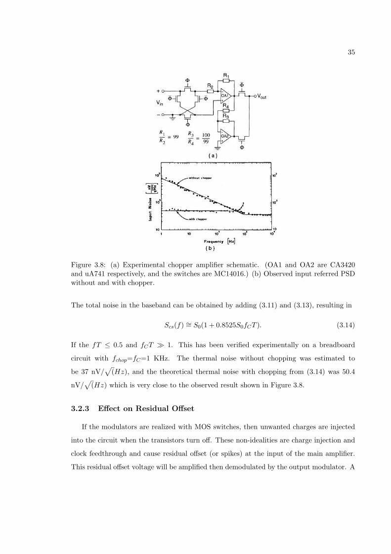
from the desired signal, Vin. . . . . . . . . . . . . . . . . . . . . . . . . . . . 313.7 Circuit implementation for chopper technique in time domain. . . . . . . . . 323.8 (a) Experimental chopper amplifier schematic. (OA1 and OA2 are CA3420
and uA741 respectively, and the switches are MC14016.) (b) Observed inputreferred PSD without and with chopper. . . . . . . . . . . . . . . . . . . . . 34
3.9 (a) Spike signal at the input signal and causing residual offset.(b) Spike signaland chopper-modulated spectra with amplifier bandwidth characteristics. . 35
3.10 First order Σ∆ ADC in discrete time domain model . . . . . . . . . . . . . 373.11 NTF plot for first order Σ∆ ADC . . . . . . . . . . . . . . . . . . . . . . . . 383.12 Input and Output of a First-Order Σ∆ ADC . . . . . . . . . . . . . . . . . 393.13 First order Σ∆ ADC in continuous time domain model . . . . . . . . . . . . 403.14 STF and NTF plot for first order Σ∆ ADC . . . . . . . . . . . . . . . . . . 403.15 A swithed-capacitor implementation of first order Σ∆ ADC . . . . . . . . . 423.16 Finite Op-Amp gain effect for NTF . . . . . . . . . . . . . . . . . . . . . . . 433.17 Excess Loop Delay . . . . . . . . . . . . . . . . . . . . . . . . . . . . . . . . 453.18 Clock jitter . . . . . . . . . . . . . . . . . . . . . . . . . . . . . . . . . . . . 453.19 Σ∆modulator with return to zero (RZ) and switched-capacitor-resistor (SRC)
feedback . . . . . . . . . . . . . . . . . . . . . . . . . . . . . . . . . . . . . . 463.20 PSD for Non returen to zero (NRZ) and SRC . . . . . . . . . . . . . . . . . 473.21 Linear model of second order Σ∆ ADC. . . . . . . . . . . . . . . . . . . . . 483.22 STF and NTF Plot. . . . . . . . . . . . . . . . . . . . . . . . . . . . . . . . 493.23 Linear model for second order Σ∆ ADC . . . . . . . . . . . . . . . . . . . . 503.24 Comparison of N=10 and N=18 bits UP-DOWN digital counter. . . . . . . 513.25 Schematic of pre-amplifier and feedback opamp. . . . . . . . . . . . . . . . . 523.26 Power spectrum density for output noise. . . . . . . . . . . . . . . . . . . . 53
4.1 First integrator. . . . . . . . . . . . . . . . . . . . . . . . . . . . . . . . . . . 574.2 Circuit implementation of pre-amplifier. . . . . . . . . . . . . . . . . . . . . 584.3 Relation between VGS − Vth and inversion coefficients i. . . . . . . . . . . . 604.4 Supply Current versus normalized noise for amplifiers. Dash lines indicate
constant NEF contours. . . . . . . . . . . . . . . . . . . . . . . . . . . . . . 614.5 Folded cascode op amp with gain boosting. . . . . . . . . . . . . . . . . . . 634.6 Gain boosting. . . . . . . . . . . . . . . . . . . . . . . . . . . . . . . . . . . 644.7 Half Circuit of folded cascode op amp. . . . . . . . . . . . . . . . . . . . . . 654.8 Additional Gian stage for boosting output impedance of PMOS current sources. 664.9 Additional Gian stage for boosting output impedance of NMOS current sources. 664.10 A conceptual block diagram of the CMFB loop. . . . . . . . . . . . . . . . . 674.11 A continuous-time CMFB circuit. . . . . . . . . . . . . . . . . . . . . . . . . 694.12 A model for slewing behavior and transient response. . . . . . . . . . . . . . 724.13 Settling Time vs. Slewing. . . . . . . . . . . . . . . . . . . . . . . . . . . . . 734.14 Settling Behavior vs. pole-zero doublet. . . . . . . . . . . . . . . . . . . . . 744.15 Implementation of DAC1. . . . . . . . . . . . . . . . . . . . . . . . . . . . . 754.16 Feedback integrator. . . . . . . . . . . . . . . . . . . . . . . . . . . . . . . . 76
viii
4.17 Op-amp for feedback integrator. . . . . . . . . . . . . . . . . . . . . . . . . 774.18 CMFB as GM stage for Overall System. . . . . . . . . . . . . . . . . . . . . 794.19 Transconductance vs. ICMR. . . . . . . . . . . . . . . . . . . . . . . . . . . 794.20 State Machine for UP-DOWN Counter. . . . . . . . . . . . . . . . . . . . . 804.21 Implementation of Feedback DAC2. . . . . . . . . . . . . . . . . . . . . . . 814.22 Implementation of Quantizer. . . . . . . . . . . . . . . . . . . . . . . . . . . 824.23 Total input referred noise. . . . . . . . . . . . . . . . . . . . . . . . . . . . . 834.24 CMRR on the top and predicted and observed PSD on the bottom. . . . . 83
5.1 Frequency Response for FIR LPF with cutoff frequency at 2000 Hz. . . . . 865.2 Output signal before and after FIR LPF and Signal Reconstruction. . . . . 865.3 Die photo for Biomedical IC . . . . . . . . . . . . . . . . . . . . . . . . . . . 875.4 Positive 0.9V and negative 0.9V for IC . . . . . . . . . . . . . . . . . . . . . 885.5 Input Attenuator . . . . . . . . . . . . . . . . . . . . . . . . . . . . . . . . . 895.6 Averaging output. . . . . . . . . . . . . . . . . . . . . . . . . . . . . . . . . 905.7 fft plot without chopping. . . . . . . . . . . . . . . . . . . . . . . . . . . . . 915.8 fft plot with chopping with input 1 mV amplitude at 100 Hz . . . . . . . . . 925.9 SNR and SNDR vs. Input Amplitude. . . . . . . . . . . . . . . . . . . . . . 935.10 Problems for 1/f noise. . . . . . . . . . . . . . . . . . . . . . . . . . . . . . . 945.11 Noise Distribution. . . . . . . . . . . . . . . . . . . . . . . . . . . . . . . . . 955.12 Noise analysis for different duty cycle. . . . . . . . . . . . . . . . . . . . . . 95

ix
List of Tables
1.1 Bio-potential signals and Applications. . . . . . . . . . . . . . . . . . . . . . 4
2.1 Specifications for Bio-potential Signals . . . . . . . . . . . . . . . . . . . . . 122.2 CMRR for different mismatching error in resistors R1 and R2, and assuming
R1 = R2 . . . . . . . . . . . . . . . . . . . . . . . . . . . . . . . . . . . . . . 21
3.1 Input referred noise for different WLs. . . . . . . . . . . . . . . . . . . . . . 303.2 First order Σ∆ ADC operation for input signal = 1/3. . . . . . . . . . . . . 41
4.1 Operating Point of Pre-Amplifier . . . . . . . . . . . . . . . . . . . . . . . . 604.2 Operating point for each transistor of op-amp. . . . . . . . . . . . . . . . . 774.3 Input Noise Summary for EEG, ECG, and EMG. . . . . . . . . . . . . . . . 834.4 Performance Summary . . . . . . . . . . . . . . . . . . . . . . . . . . . . . . 84
5.1 Components for 0.9V and -09V. . . . . . . . . . . . . . . . . . . . . . . . . . 895.2 Signal and Noise powers summary. . . . . . . . . . . . . . . . . . . . . . . . 935.3 Total input referred noise for different duty cycles. . . . . . . . . . . . . . . 965.4 Performance Summary. . . . . . . . . . . . . . . . . . . . . . . . . . . . . . . 97

1
Chapter 1
Introduction
Various clinical and scientific disciplines sense the electrical activity associated with
various functions of the human body through electrophysiological signals such as Electroen-
cephalogram (EEG), Electrocardiogram (ECG), and Electromyogram (EMG). At present,
different instrumentation is designed for each electrophysiologic signal. This work presents
a mixed-signal integrated circuit (IC) prototype to provide complete, programmable analog
conditioning and analog-to-digital conversion suitable for a range of electrophysiologic sig-
nals. Section 1.1 of this chapter gives an overview and background of bio-potential signals.
Section 1.2 describes the goals of this project. Section 1.3 describes the existing work as of
project initiation in 2006. Finally, Section 1.4 presents the existing work in 2010 at project
completion.
This thesis is organized as follows; Chapter 2 covers the design specifications required
in order to extract weak bio-potential signals, over different frequency ranges, in the pres-
ence of large in-band and out-of-band interference. Chapter 3 describes the Sigma-Delta
(Σ∆) analog-to-digital converter (ADC) architecture developed for this work, with a pro-
grammable built-in pre-amplifier to meet the design requirements for different signal appli-
cations. Sources of error, nonidealities, and their effects on the digital output are discussed.
Chapter 4 covers the detailed circuit implementation of the Σ∆ ADC. Chapter 5 presents
the results from the prototype IC fabricated in a 180nm CMOS process. Chapter 6 con-
cludes by summarizing the developments and contributions of the thesis and possible future
2
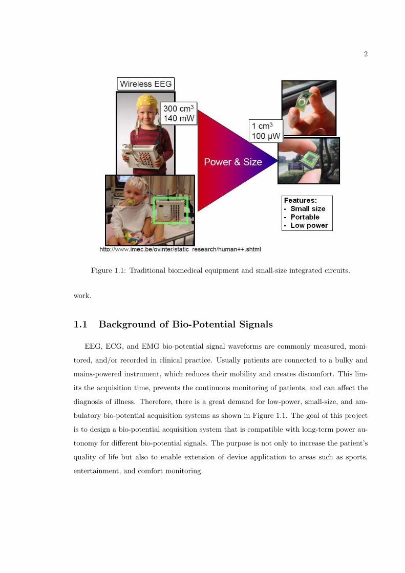
Figure 1.1: Traditional biomedical equipment and small-size integrated circuits.
work.
1.1 Background of Bio-Potential Signals
EEG, ECG, and EMG bio-potential signal waveforms are commonly measured, moni-
tored, and/or recorded in clinical practice. Usually patients are connected to a bulky and
mains-powered instrument, which reduces their mobility and creates discomfort. This lim-
its the acquisition time, prevents the continuous monitoring of patients, and can affect the
diagnosis of illness. Therefore, there is a great demand for low-power, small-size, and am-
bulatory bio-potential acquisition systems as shown in Figure 1.1. The goal of this project
is to design a bio-potential acquisition system that is compatible with long-term power au-
tonomy for different bio-potential signals. The purpose is not only to increase the patient’s
quality of life but also to enable extension of device application to areas such as sports,
entertainment, and comfort monitoring.

3
1.2 Research Goal
EEG is used primarily in studying the properties of cerebral and neural networks in
neurosciences, as well as to monitor the neurodevelopment and sleep patterns of infants in
the intensive care unit and ultimately to use this information to improve daily medical care.
EEG is also used to monitor epileptic seizures from patients.
The ECG is a diagnostic tool that measures and records the electrical activity of the
heart. Interpretation of ECG waveform details allows diagnosis of a wide range of heart
conditions, varying from minor to life threatening (e.g. symptoms of myocardial infarction).
ECG is also used for assessment of patients with systemic disease or critical conditions, as
well as patient monitoring during anesthesia.
EMG is a technique for evaluating and recording the electrical activity produced by
skeletal muscles. It is used to diagnose diseases that generally may be classified into follow-
ing categories: neuropathies, neuromuscular junction diseases and myopathies. Table 1.1
summaries the selected applications for differential bio-potential signals.
Bio-potential signals such as EEG, ECG, and EMG are considered to be weak signals
since peak amplitudes range from 100 µV in the case of EEG signals up to 5 mV for ECG
signals [1]. The bandwidth of these bio-potential signals ranges from 0.05 to 2000Hz in nor-
Figure 1.2: Frequency and amplitude characteristics of bio-potential signals, EEG, ECG,and EMG, and contaminating signals of the bio-potential signals.
4
Table 1.1: Bio-potential signals and Applications.
Bio-potential signals Selected Applications
EEG Sleep studies, seizure detection, cortical mapping
ECG Diagnosis of ischemia, arrhymia, conduction defects
EMG Eye position, sleep state, vetibulo-ocular reflex
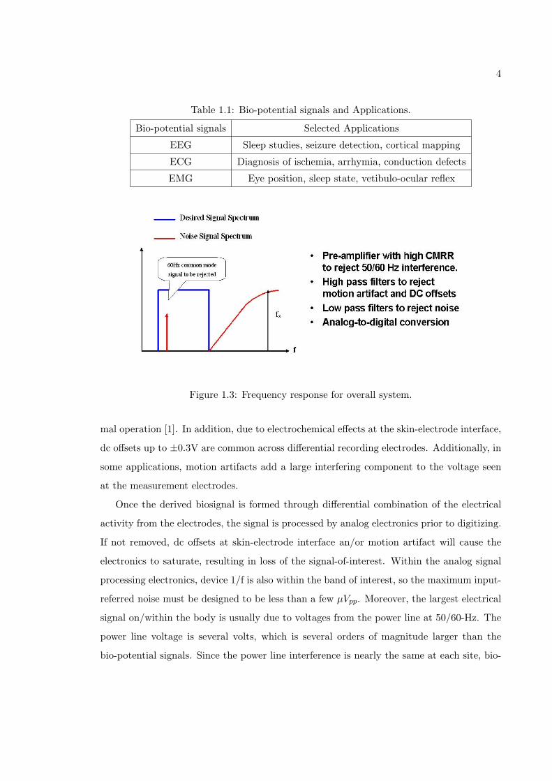
Figure 1.3: Frequency response for overall system.
mal operation [1]. In addition, due to electrochemical effects at the skin-electrode interface,
dc offsets up to ±0.3V are common across differential recording electrodes. Additionally, in
some applications, motion artifacts add a large interfering component to the voltage seen
at the measurement electrodes.
Once the derived biosignal is formed through differential combination of the electrical
activity from the electrodes, the signal is processed by analog electronics prior to digitizing.
If not removed, dc offsets at skin-electrode interface an/or motion artifact will cause the
electronics to saturate, resulting in loss of the signal-of-interest. Within the analog signal
processing electronics, device 1/f is also within the band of interest, so the maximum input-
referred noise must be designed to be less than a few µVpp. Moreover, the largest electrical
signal on/within the body is usually due to voltages from the power line at 50/60-Hz. The
power line voltage is several volts, which is several orders of magnitude larger than the
bio-potential signals. Since the power line interference is nearly the same at each site, bio-

5
Figure 1.4: Typical Instrumentation amplifier with 3-op amp configuration.
potential signals tend to be acquired using a weighted, balanced electrode configuration.
Then the common mode of electrical activity from two sites can be subtracted and the
differential mode of these is amplified.
A summary of measurement source errors is shown in Figure 1.2. In order to achieve
signal extraction under these circumstances, an acquisition system must be designed with
high common-mode rejection ration (CMRR), low noise, and a high-pass filter (HPF) char-
acteristics as shown in Figure 1.3.
1.3 Existing Work, as of 2006
In this section, several design alternatives are investigated for a bio-potential signal
acquisition system. An instrumentation amplifier (IA) is used in many applications, from
motor control to data acquisition to automotive. Figure 1.4 shows a typical 3-op amp IA
configuration [2]. The input amplifiers A1 and A2 of the IA buffer the input voltage. A
single resistor, Rgain, is connected between the summing nodes of the two input buffers.
6
The full differential input voltage will now appear across Rgain. Since the amplified input
voltage appears differentially across the three resistors R1 - Rgain - R1, the differential gain
can be varied by changing Rgain.The total gain of the circuit is
Vout
Vin=
(1 +
2R1
Rgain
)R3
R2. (1.1)
Since the voltage acrossRgain equals Vin, the current throughRgain will equal (Vin/Rgain).
Amplifiers A1 and A2 will operate with gain and amplify the input signal. If a common-
mode voltage is applied to the amplifier input, the voltages on each side of Rgain will be
equal, and no current will flow through this resistor. Since no current flows through Rgain,
amplifiers A1 and A2 will operate as unity-gain followers. Thus, common-mode signals will
be passed through the input buffers at unity gain, but differential voltages will be amplified
by the factor (1 + 2R1/Rgain). Finally, the common-mode voltages are attenuated by the
subtractor A3 while the differential voltages are amplified by a factor of R3/R2. In order to
process the weak bio-potential signals, the buffer amplifiers must be designed with low input
referred noise. One of the R3 resistors can be adjustable to maintain high common-mode
rejection due to the mismatch between the two R2 / R3 resistor ratios.
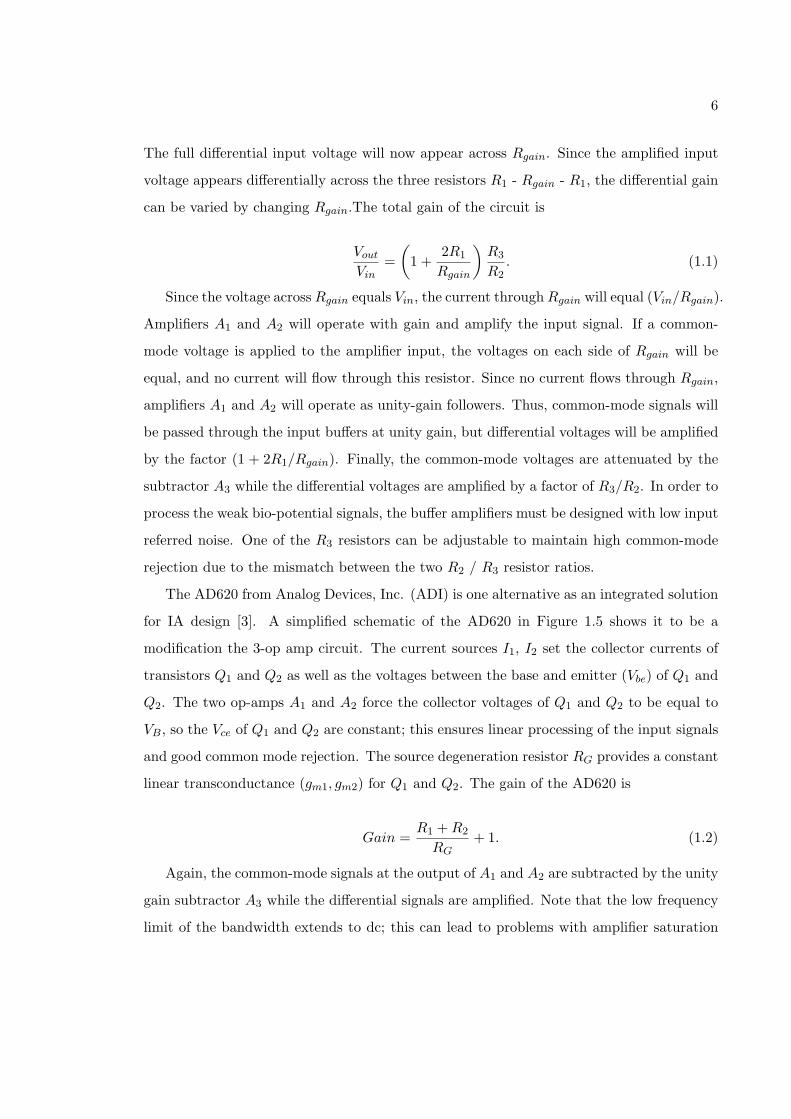
The AD620 from Analog Devices, Inc. (ADI) is one alternative as an integrated solution
for IA design [3]. A simplified schematic of the AD620 in Figure 1.5 shows it to be a
modification the 3-op amp circuit. The current sources I1, I2 set the collector currents of
transistors Q1 and Q2 as well as the voltages between the base and emitter (Vbe) of Q1 and
Q2. The two op-amps A1 and A2 force the collector voltages of Q1 and Q2 to be equal to
VB, so the Vce of Q1 and Q2 are constant; this ensures linear processing of the input signals
and good common mode rejection. The source degeneration resistor RG provides a constant
linear transconductance (gm1, gm2) for Q1 and Q2. The gain of the AD620 is
Gain =R1 +R2
RG+ 1. (1.2)
Again, the common-mode signals at the output of A1 and A2 are subtracted by the unity
gain subtractor A3 while the differential signals are amplified. Note that the low frequency
limit of the bandwidth extends to dc; this can lead to problems with amplifier saturation

7
Figure 1.5: A simplified schematic of the AD620.
given the large dc errors indicated in Figure 1.2.
As of project initiation in 2006, recent work on bio-amplifier design [4–13] featured AC-
coupled input circuitry with a MOS-Bipolar “pseudoresistor” to obtain a low-frequency
cutoff that passes the signal of interest while rejecting large dc offsets. A MOS-Bipolar
pseudoresistor can achieve an equivalent resistance req of greater than 1010Ω [4]. A typical
schematic of this bio-amplifier design approach is shown at the left of Figure 1.6. The
midband gain AM is set by C1/C2, and the bandwidth is gm/(AMCL), where C1 and C2
are the feedback network capacitors, and gm is the transconductance of the operational
transconductance amplifier (OTA). Two MOS-bipolar pseudoresistors are used in serial to
reduce the distortion for large output signals, while any dc signals are rejected by the
capacitor C1. The low-frequency cutoff of the ac-coupled amplifier is 1/(2reqC2). The
measured amplifier transfer function from 0.004Hz to 50 kHz is shown at the right of Figure
1.6. The midband gain is approximately 40dB. The low-frequency cutoff is approximately
0.025 Hz. The input-referred noise of the bio-amplifier can be related to the (OTA) input-
referred noise by
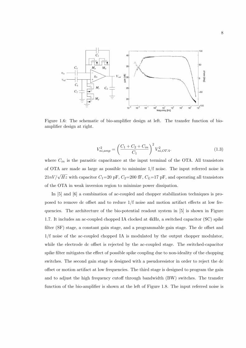
8
Figure 1.6: The schematic of bio-amplifier design at left. The transfer function of bio-amplifier design at right.
V 2ni,amp =
(C1 + C2 + Cin
C1
)2
V 2ni,OTA. (1.3)
where Cin is the parasitic capacitance at the input terminal of the OTA. All transistors
of OTA are made as large as possible to minimize 1/f noise. The input referred noise is
21nV/√Hz with capacitor C1=20 pF, C2=200 fF, CL=17 pF, and operating all transistors
of the OTA in weak inversion region to minimize power dissipation.
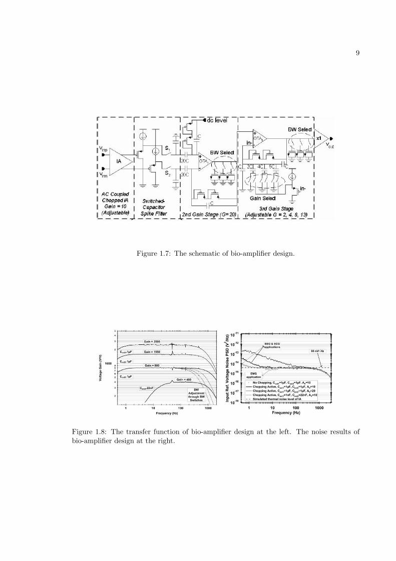
In [5] and [6] a combination of ac-coupled and chopper stabilization techniques is pro-
posed to remove dc offset and to reduce 1/f noise and motion artifact effects at low fre-
quencies. The architecture of the bio-potential readout system in [5] is shown in Figure
1.7. It includes an ac-coupled chopped IA clocked at 4kHz, a switched capacitor (SC) spike
filter (SF) stage, a constant gain stage, and a programmable gain stage. The dc offset and
1/f noise of the ac-coupled chopped IA is modulated by the output chopper modulator,
while the electrode dc offset is rejected by the ac-coupled stage. The switched-capacitor
spike filter mitigates the effect of possible spike coupling due to non-ideality of the chopping
switches. The second gain stage is designed with a pseudoresistor in order to reject the dc
offset or motion artifact at low frequencies. The third stage is designed to program the gain
and to adjust the high frequency cutoff through bandwidth (BW) switches. The transfer
function of the bio-amplifier is shown at the left of Figure 1.8. The input referred noise is
9
Figure 1.7: The schematic of bio-amplifier design.
Figure 1.8: The transfer function of bio-amplifier design at the left. The noise results ofbio-amplifier design at the right.

10
Figure 1.9: Simplified AD8553 schematic.
56nV/√Hz and is shown at the right of Figure 1.8.
Following demonstration of single channel biomedical acquisition systems, multi-channel
systems [8, 10–12] have been designed based on the AC-coupled with pseudoresistor tech-
nique, and also [11] using the chopping technique.
1.4 Existing Work as of 2010
As the work of this thesis was nearing completion in 2010, Analog Devices released the
AD8553 product for single channel systems with gain set by two off-chip resistors R1 and
R2 based on the fundamental concept of 3-op amp IA topology. White noise is defined by
the off-chip resistors R1 and R2, and transconductances of transistors M1 and M2 as shown
in Figure 1.9. 1/f noise is reduced by an autocorrelation shuffling technique.
As shown in Figure 1.9, the circuit consists of a voltage-to-current converter (M1 to M6),
followed by a current-to-voltage amplifier (R2 and A1). When an input signal is applied,
the differential-mode voltage is converted to a current in R1. Transistors M3 to M6 form
a folded cascode structure which provides twice this current to the input of the opamp
A1. Amplifier A1 and resistor R2 form a current-to-voltage converter to generate a output

11
voltage at VOUT . Since common-mode input voltage does not contribute to current in R1,
the current IR inherently rejects the input common-mode voltage so it is not seen by the
voltage-to-current amplifier. The external capacitor C2 aattenuates high frequency noise.
Also in 2010, Texas instruments (TI) released the ADS1298, an 8-channel product with
programmable gain amplifier (PGA) and 24-bit Σ∆ ADC for biomedical applications. The
functional block diagram of ADS1298 is shown in Figure 1.10 (Σ∆ ADC is not shown).
Each channel contains an EMI filter, a flexible input multiplexer, a PGA, and a Σ∆ ADC.
The EMI filter is designed with cutoff frequency at 3 MHz to filter out any electromagnetic
interference that may have been coupled to/from signal or power lines. The PGA is designed
with low-noise, gain programmable based on the traditional 3-op amp configuration. The
right leg drive (RLD) circuity is used as a negative feedback loop to reduce the effect of
common mode signal from the power line. Once the bio-potential signals are extracted, the
Σ∆ ADC converts the analog signal to digital format. Thus, it can be digitally networked
with many other of these ICs.
Both AD8553 and ADS1298 are good examples of single and multi-channel systems for
biomedical applications, similar to the work to be described in this thesis. More detailed
specifications for these products can be found in [14,15].

12
Figure 1.10: Functional block diagram of ADS1298.

13
Chapter 2
Analog Architecture Requirement
In this chapter, analog architecture requirements for biomedical acquisition system are
introduced. Table 2.1 summaries the specifications for bio-potential signals. Section 2.1
introduces the bandwidth requirement for these signals. Section 2.2 states the noise from
different sources. Section 2.3 and section 2.4 describes the CMRR and input common-mode
range (ICMR) requirements for the system respectively.
2.1 Bandwidth
The bandwidth for bio-potential signals ranges from 0.05 Hz to 2000 Hz according to
Table 2.1. A system with high-pass filter (HPF) and low-pass filter (LPF) characteristics is
needed in order to meet the requirement. However, a HPF with 0.05 Hz cutoff frequency is
not easy to achieve, as a large value resistor or capacitor is required in order to realize a low
Table 2.1: Specifications for Bio-potential Signals
ECG EEG EMG
Amplitude (mV) 1 0.1 1
Frequency Range (Hz) 0.05-100 0.1-100 100-2000
Noise (uVrms) ≤2.5 ≤2.5 ≤1.6
CMRR (dB) ≥85
ICMR (V) ±0.3
14
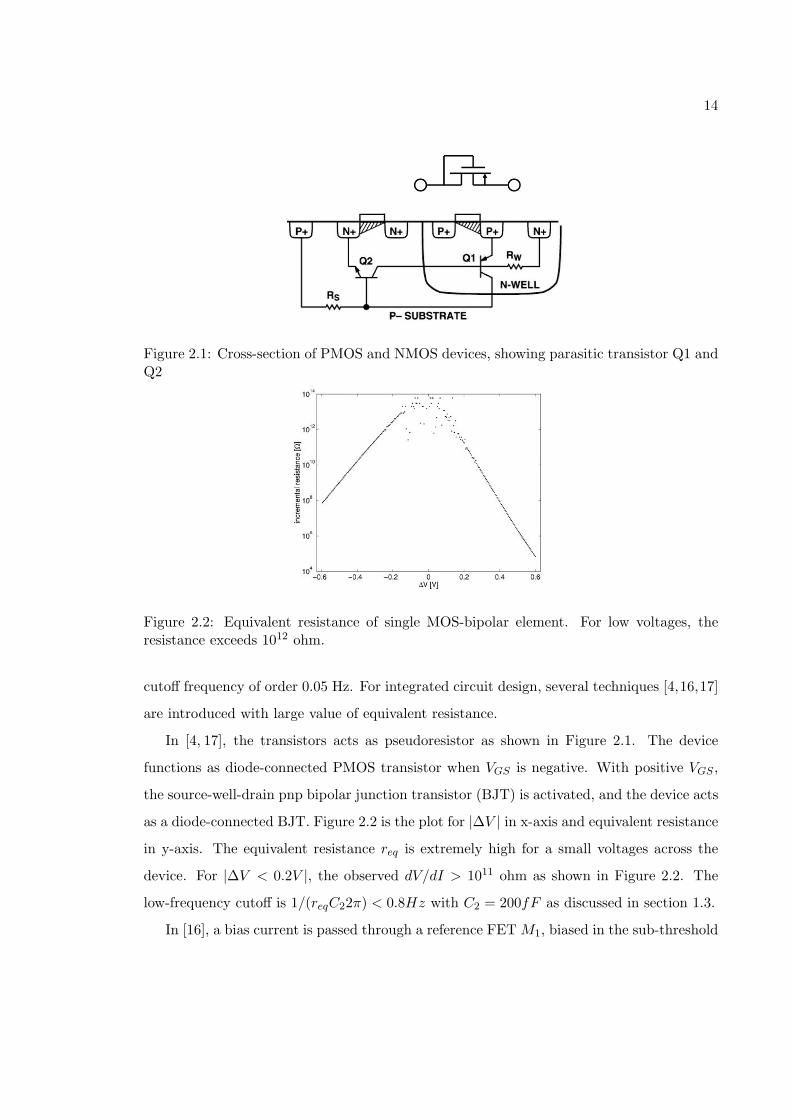
Figure 2.1: Cross-section of PMOS and NMOS devices, showing parasitic transistor Q1 andQ2
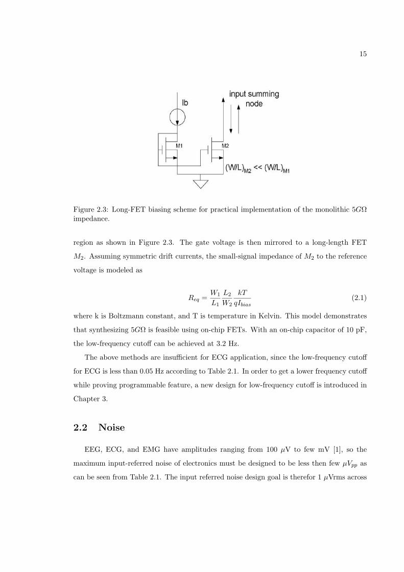
Figure 2.2: Equivalent resistance of single MOS-bipolar element. For low voltages, theresistance exceeds 1012 ohm.
cutoff frequency of order 0.05 Hz. For integrated circuit design, several techniques [4,16,17]
are introduced with large value of equivalent resistance.
In [4, 17], the transistors acts as pseudoresistor as shown in Figure 2.1. The device
functions as diode-connected PMOS transistor when VGS is negative. With positive VGS ,
the source-well-drain pnp bipolar junction transistor (BJT) is activated, and the device acts
as a diode-connected BJT. Figure 2.2 is the plot for |∆V | in x-axis and equivalent resistance
in y-axis. The equivalent resistance req is extremely high for a small voltages across the
device. For |∆V < 0.2V |, the observed dV/dI > 1011 ohm as shown in Figure 2.2. The
low-frequency cutoff is 1/(reqC22π) < 0.8Hz with C2 = 200fF as discussed in section 1.3.
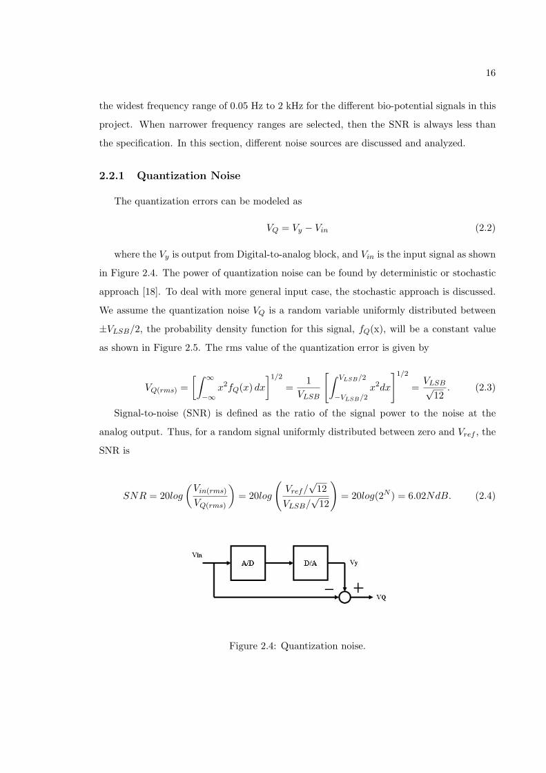
In [16], a bias current is passed through a reference FET M1, biased in the sub-threshold
15
Figure 2.3: Long-FET biasing scheme for practical implementation of the monolithic 5GΩimpedance.
region as shown in Figure 2.3. The gate voltage is then mirrored to a long-length FET
M2. Assuming symmetric drift currents, the small-signal impedance of M2 to the reference
voltage is modeled as
Req =W1
L1
L2
W2
kT
qIbias(2.1)
where k is Boltzmann constant, and T is temperature in Kelvin. This model demonstrates
that synthesizing 5GΩ is feasible using on-chip FETs. With an on-chip capacitor of 10 pF,
the low-frequency cutoff can be achieved at 3.2 Hz.
The above methods are insufficient for ECG application, since the low-frequency cutoff
for ECG is less than 0.05 Hz according to Table 2.1. In order to get a lower frequency cutoff
while proving programmable feature, a new design for low-frequency cutoff is introduced in
Chapter 3.
2.2 Noise
EEG, ECG, and EMG have amplitudes ranging from 100 µV to few mV [1], so the
maximum input-referred noise of electronics must be designed to be less then few µVpp as
can be seen from Table 2.1. The input referred noise design goal is therefor 1 µVrms across
16
the widest frequency range of 0.05 Hz to 2 kHz for the different bio-potential signals in this
project. When narrower frequency ranges are selected, then the SNR is always less than
the specification. In this section, different noise sources are discussed and analyzed.
2.2.1 Quantization Noise
The quantization errors can be modeled as
VQ = Vy − Vin (2.2)
where the Vy is output from Digital-to-analog block, and Vin is the input signal as shown
in Figure 2.4. The power of quantization noise can be found by deterministic or stochastic
approach [18]. To deal with more general input case, the stochastic approach is discussed.
We assume the quantization noise VQ is a random variable uniformly distributed between
±VLSB/2, the probability density function for this signal, fQ(x), will be a constant value
as shown in Figure 2.5. The rms value of the quantization error is given by
VQ(rms) =
[∫ ∞
−∞x2fQ(x) dx
]1/2=
1
VLSB
[∫ VLSB/2
−VLSB/2x2dx
]1/2=
VLSB√12
. (2.3)
Signal-to-noise (SNR) is defined as the ratio of the signal power to the noise at the
analog output. Thus, for a random signal uniformly distributed between zero and Vref , the
SNR is
SNR = 20log
(Vin(rms)
VQ(rms)
)= 20log
(Vref/
√12
VLSB/√12
)= 20log(2N ) = 6.02NdB. (2.4)
Figure 2.4: Quantization noise.

17
Figure 2.5: Probability density function for the quantization error.
where N is number of bit of analog-to digital converter (ADC). However, a input sinusoidal
waveform between zero and Vref is more commonly used in many applications. The SNR
is then given by
SNR = 20log
(Vin(rms)
VQ(rms)
)= 20log
(Vref/2
√2
VLSB/√12
)= 20log
(√3
22N
)= 6.02N + 1.76dB.
(2.5)
2.2.2 Thermal Noise
The random motion of electrons in a conductor introduces thermal noise. Thus, the
thermal noise power is proportional to the absolute temperature. In a resistor R, thermal
noise power can be modeled by a series voltage source V 2 or by a shunt current generator
i2 as shown in Figure 2.6. These representations are equivalent and
v2 = 4kTR∆f (2.6)
i2 = 4kT1
R∆f (2.7)
For MOS transistor, the resistive channel under gate is modulated by the gate-source
voltage so that the drain current is controlled by the gate-source voltage. Since the channel
material is resistive, it exhibits thermal noise. It can be proved [19] that for long-channel
MOS devices operating in saturation region, the channel noise can be modeled by a current
source connected between the drain and source terminals with a spectrum density:

18
Figure 2.6: Alternative representations of thermal noise.
I2n = 4kTγ/Rch (2.8)
where Rch is channel resistance, and γ is equal to 2/3 for long-channel transistors and may
vary with different technologies.
There has been some work on modeling thermal noise for short-channel trnasistors [20–
22]. However, the thermal noise behavior of short-channel MOSFETs in the saturation
region is not well understood and controversial. The theoretical determination of γ is still
under research. Since this project is implemented with CMOS 0.18um technology, the γ is
assumed to be equal 2/3 with hand analysis and then be verified by simulation. The Rch
in (2.8) is also equal to 1/gm, where gm is transconductance of MOS transistor. A more
general expression of thermal noise for MOSFETs is also given
V 2n =
8
3kT
1
gm(2.9)
2.2.3 1/f Noise
In the MOSFET, 1/f noise is caused mainly by the random trapping and detrapping
process of charges in the oxide traps associated with contamination and crystal defects near
the Si−SiO2 interface. The charge fluctuation results in fluctuation of the surface potential

19
Figure 2.7: 1/f noise corner frequency.
and thus modulates the channel carrier density. Since the carrier lifetime in silicon is on the
order of tens of microseconds, the resulting current fluctuations are concentrated at lower
frequencies [23]. Typically PMOS transistors have less 1/f noise than NMOS transistors
since their majority carriers (holes) are less likely to be trapped. The average power of 1/f
noise cannot be predicted easily, it depends on the “cleanness” of the oxide-silicon interface.
The 1/f noise can be modeled as a voltage source in series the gate and roughly given by
V 2n =
K
CoxWL
1
f(2.10)
where K is a process-dependent constant and depends on device characteristics, Cox is gate
oxide capacitance per unit area, and WL is the area for MOS transistor. An important
point to note here is that the 1/f noise is inversely proportional to the transistor area, WL.
In other words, larger devices results in less 1/f noise. 1/f noise is extremely important in
biomedical applications, because it typically dominates at low frequencies. If we plot both
thermal noise and 1/f noise on the same axes as shown in Figure 2.7, the intersection point
between both noise sources is called 1/f noise corner frequency. The 1/f noise corner, fC ,
can be found as8
3kT
1
gm=
K
CoxWL
1
fC, (2.11)
that is,
fC =K
CoxWLgm
3
8kT. (2.12)

20
Figure 2.8: Schematic of Differential Amplifier.
This implies that fC depends on the device dimensions WL and bias current through gm.
Thus, the tradoff between noise and power or die area are challenges for circuit design.
Chopping techniques for 1/f reduction is widely used in biomedical application [6,7,24,
25]. In this project, this technique is applied, and the detailed description is given in next
chapter.
2.3 Common Mode Rejection Ratio
The common mode signal at 50/60 Hz from power line is another noise for bio-potential
signal acquisition system. Thus, an IA is designed with high CMRR to reject any common
mode signals from outside world. The CMRR is defined as [26]
CMRR =ADM
ACM. (2.13)
where ADM is differential gain, and ACM is common mode gain. A good example of
high CMRR design is the traditional 3-op IA as discussed in Chapter 1. A key point of
this topology is the differential amplifier or subtractor for common-mode signal rejection
and differential-mode signal amplification. The ACM of differential amplifier is zero, if

21
R1(1 − k) = R1(1 + k), and R2(1 − k) = R2(1 + k) with k =0 as shown in Figure 2.8,
where k is individual resistor tolerance in fractional form. If the resistors R1 and R2 are
not matched well, and V1 = V2 = Vcm, the voltages Va and Vb can be found by
Va =R2(1 + k)
R1(1− k) +R2(1 + k)Vcm. (2.14)
Vb =R2(1− k)
R1(1 + k) +R2(1− k)Vcm. (2.15)
since the error voltage Vecm at the input terminals of amplifier is equal to Va − Vb, the
output voltage Vocm due to Vecm can be expressed as
Vocm = Vecm × R1 (1− k) +R2 (1 + k)
R1 (1− k)
= Vcm
(R2 (1 + k)
R1 (1− k) +R2 (1 + k)− R2 (1− k)
R1 (1 + k) +R2 (1− k)
)×
(R1 (1− k) +R2 (1 + k)
R1 (1− k)
)(2.16)
Thus, the common gain ACM is
ACM =Vocm
Vcm
=
(R2 (1 + k)
R1 (1− k) +R2 (1 + k)− R2 (1− k)
R1 (1 + k) +R2 (1− k)
)(R1 (1− k) +R2 (1 + k)
R1 (1− k)
)=
R2
R1
(1 + k
1− k− R1 (1− k) +R2 (1 + k)
R1 (1 + k) +R2 (1− k)
)=
R2
R1
((1 + k)2R1 − (1− k)2R1
R1 (1 + k) (1− k) +R2 (1− k)2
)∼=
R2
R1
4kR1
R1 +R2
∼=4kR2
R1 +R2(2.17)
Since the differential gain ADM = R2/R1, the CMRR is

22
Table 2.2: CMRR for different mismatching error in resistors R1 and R2, and assumingR1 = R2
k 1% 0.1% 0.01% 0.001%
CMRR (dB) 34 54 74 94
CMRR =ADM
ACM
=R2
R1
R1 +R2
4kR2
=
(1 +
R2
R1
)1
4k(2.18)
With a mismatching error of k=1% in resistor ratios, the CMRR is 34 dB using (2.18),
and assuming R1 = R2. Table 2.2 summaries the CMRR corresponding to the percentage
error of k in resistor ratios. According to the table 2.2, the mismatching error k should be
less than 0.01% in order to meet the specification. Due to mismatching between resistors,
an error voltage Vir at the input is generated and can be obtained by
Vir =VIN
CMRRr. (2.19)
Thus, the error voltage at the output Vor can be expressed by
Vor =1
β(VIN − Vir)
=1
β
(1− 1
CMRRr
)VIN (2.20)
where β is R1/(R1 +R2), and CMRRr is CMRR due to mismatching between resistors. If
there is another offset voltage at the input due to the amplifier gain error, the total output
voltage error is then given by
Vor =1
β
(1−
(1
CMRRa+
1
CMRRr
))VIN
=1
β
(1− 1
CMRRTotal
)VIN (2.21)
where CMRRa are CMRR for amplifier gain error, and 1/CMRRTotal = 1/CMRRr +
1/CMRRa. Since most of IA design are differential topology, the mismatching between
input stages should be carefully considered.

23
2.4 Input Common Mode Range
Due to electrochemical effects at the skin-electrode interface, dc offsets of ±0.3 V are
common across differential recording electrodes [1]. An IA with wide input common mode
range is needed in order to reject the common mode interference of ±0.3 V. Source degen-
eration is widely used to provide good linearity over wide input common range [27,28]. The
schematic of a typical source degeneration design for bio-medical applications is shown at
the left of Figure 2.9. The transconductance gm is 2/Rin and is linear over a wide input
common mode range. However, the noise at the input due to the extra resistor Rin is
increased to 4kTRin/2.
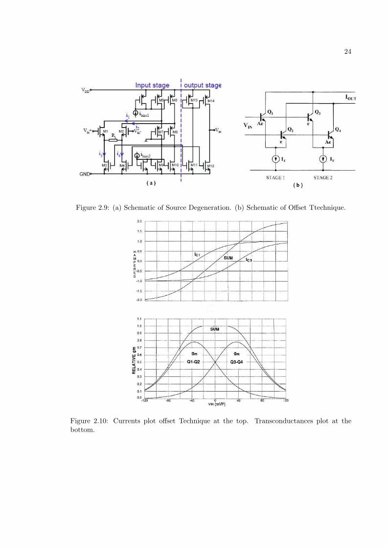
Another technique to improve linearity is also presented in [29, 30]. The basic idea is
to generate an offset voltage at the inputs by sizing the different transistors Q1 and Q3 as
shown at the right of Figure 2.9. The output currents IC1 and IC3 are plotted at the top of
Figure 2.10 when a differential input voltage is applied. The current ISUM is the summation
of IC1 and IC3. The total transconductance gm is derivative of ISUM with respective to
input voltage and is plotted at the bottom of Figure 2.10. As a result, the transconductance
gm is linear over an input range ±40 mV. However, the total noise is almost twice that of
a single differential pair.
In this thesis, one major novel contribution is the design of a pre-amplifier, described
in chapter 4, with wide input common mode range and high CMRR in order to meet the
specifications based on the requirements of Table 2.1.
24
Figure 2.9: (a) Schematic of Source Degeneration. (b) Schematic of Offset Ttechnique.
Figure 2.10: Currents plot offset Technique at the top. Transconductances plot at thebottom.

25
Chapter 3
Sigma-Delta ADC Architecture
Several topologies for bio-potential applications are investigated in Chapter .1. With
traditional 3-op amp IA or AD620 IA design [2], the resistors mismatching is an issue for
high CMRR as discussed in section 2.3. Lower mismatching resistors can be achieved by
trimming technique, however, it increases the budget for the project. An ADC is also needed
to digitize the analog signal to digital format, and to communicate over shared digital buses.
The AC-couple with pseudoresistor is also discussed in Chapter .1 [4]. The impedance of
pseudoresistor is lack of control to provide the selection for different applications. Moreover,
an ADC is required to convert the analog signal to digital format for sharing by other such
ICs. Since the goal of this project is to design an IC for portable biomedical application,
low power design should also be considered.
The AD8553 is presented in Chapter .1 [14]. Source degeneration technique is used
based on the idea of 3-op amp IA configuration. The product is designed from 1.8V to
5.5V power supplies with total current of 4 uA and input referred noise of 0.7 uVp-p from
0.01Hz to 10Hz. Although an IA can be designed with 1.8V power supply in 0.18um CMOS
technology by this topology, extra circuitry is needed to program the bandwidth selection
for different biomedical applications. An ADC again is also needed to translate the analog
signal to digital signal.
A conventional Σ∆ ADC has LPF characteristic for the signal transfer function, which
can saturate the integrator to most positive supply rail and severely degrade dynamic range

26
Figure 3.1: Overall System Block
due to the large offset generated at the skin-electrode interface. Thus, a 24-bit Σ∆ ADC for
bio-potential acquisition system is not sufficient without an isolated buffer or HPF in the
front-end. Therefore, a front-end with a buffer or HPF characteristic is needed to process
very weak biomedical signals. Figure 3.1 shows the proposed Σ∆ ADC with inherent HPF
signal conditioning stage. The overall system consists of an integrator and quantizer as in
a conventional Σ∆ ADC, a differential difference pre-amplifier, and a feedback path with a
controllable UP-DOWN counter, integrator, transconductance Gm stage, and FIR LPF.
The pre-amplifier is designed with low input referred noise 1 µVrms and high CMRR.
The Gm stage provides cancellation of input common signals while alleviating the dc offsets
due to electrochemical effects at the electrode-tissue interface. The first integrator, second
integrator, a UP-DOWN digital counter, and a quantizer form the architecture of a second
order Σ∆ ADC. The UP-DOWN counter acts as a programmable attenuator in the feedback
path, since a total of 2N digital counts must be accumulated before the feedback DAC2 bit
is activated.
This chapter is organized as follows: Section 3.1 and section 3.2 state the reasons that Σ∆
ADC and chopping technique are selected for the overall system. Section 3.3 and section

27
Figure 3.2: ADC architectures, applications, resolution, and sampling rates.
3.4 present the behavior of first order and second order Σ∆ ADC respectively. Final, a
summary is given in Section 3.5
3.1 Motivation for Sigma-Delta ADC
ADCs can be categorized into two types based on the sampling frequency: Nyquist
ADC and Oversampling ADC [31]. The Nyquist ADC requires that the sampling frequency
be at least twice the highest frequency of signal. If the sampling frequency is less than
twice the maximum signal frequency, the signal will be lost and the phenomena is called
aliasing. The quantization noise of Nyquist ADC is evenly spread over the frequency and
SNR can be obtained by (2.5). For Oversampling ADC, the samping frequency is much
higher than Nyquist ADC, and its quantization noise is pushed into high frequencies with
the noise shaping property of Oversampling ADC. Thus, the SNR is different from (2.5)
and is analyzed in sections 3.3 and 3.4. As a result, the resolution of oversampling ADC is
higher than Nyquist ADC.
The most popular ADC architectures today for Nyquist ADC are successive-approximation-
register ADC (SAR), flash, pipelined ADC, and Σ∆ ADC for Oversampling ADC. All ADC
28
require one or more steps involving comparison of an input signal with a reference. Fig-
ure 3.2 shows how flash, pipelined, SAR, and Σ∆ architectures differ with respect to the
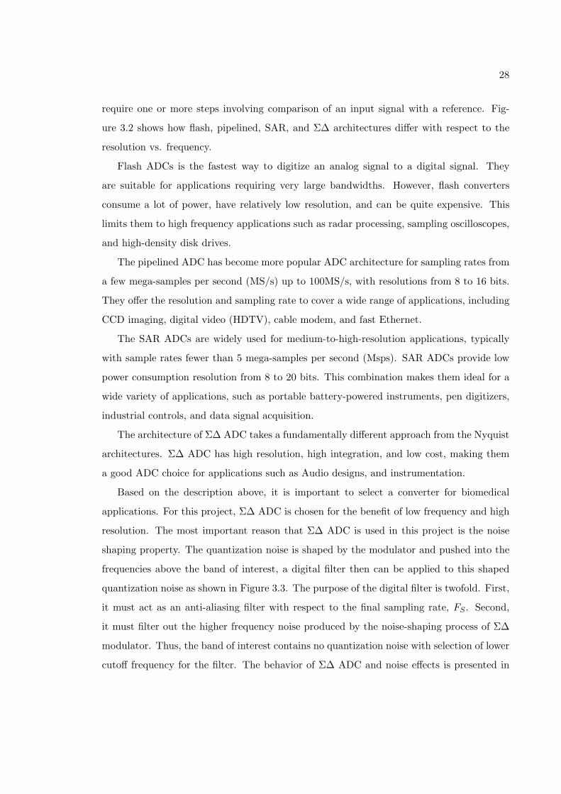
resolution vs. frequency.
Flash ADCs is the fastest way to digitize an analog signal to a digital signal. They
are suitable for applications requiring very large bandwidths. However, flash converters
consume a lot of power, have relatively low resolution, and can be quite expensive. This
limits them to high frequency applications such as radar processing, sampling oscilloscopes,
and high-density disk drives.
The pipelined ADC has become more popular ADC architecture for sampling rates from
a few mega-samples per second (MS/s) up to 100MS/s, with resolutions from 8 to 16 bits.
They offer the resolution and sampling rate to cover a wide range of applications, including
CCD imaging, digital video (HDTV), cable modem, and fast Ethernet.
The SAR ADCs are widely used for medium-to-high-resolution applications, typically
with sample rates fewer than 5 mega-samples per second (Msps). SAR ADCs provide low
power consumption resolution from 8 to 20 bits. This combination makes them ideal for a
wide variety of applications, such as portable battery-powered instruments, pen digitizers,
industrial controls, and data signal acquisition.
The architecture of Σ∆ ADC takes a fundamentally different approach from the Nyquist
architectures. Σ∆ ADC has high resolution, high integration, and low cost, making them
a good ADC choice for applications such as Audio designs, and instrumentation.
Based on the description above, it is important to select a converter for biomedical
applications. For this project, Σ∆ ADC is chosen for the benefit of low frequency and high
resolution. The most important reason that Σ∆ ADC is used in this project is the noise
shaping property. The quantization noise is shaped by the modulator and pushed into the
frequencies above the band of interest, a digital filter then can be applied to this shaped
quantization noise as shown in Figure 3.3. The purpose of the digital filter is twofold. First,
it must act as an anti-aliasing filter with respect to the final sampling rate, FS . Second,
it must filter out the higher frequency noise produced by the noise-shaping process of Σ∆
modulator. Thus, the band of interest contains no quantization noise with selection of lower
cutoff frequency for the filter. The behavior of Σ∆ ADC and noise effects is presented in

29
Figure 3.3: Effects of digital filtering on shaped quantization noise
section 3.3 and 3.4.
3.2 Motivation for Chopping
According the section 2.2.3, 1/f noise is inside the band of interest. Moreover, the DC
offsets due to the input stage mismatching will degrade the performance of CMRR. Since
bio-potential signals are located between 0.05-2000 Hz, the effects of 1/f noise and DC offsets
are significant challenges to the circuit design. Autozeroing and chopping technique are
widely used to reduce the noise at low frequency [24,32]. A clear distinction is made between
autozeroing, which is sampling technique, and chopping, which is modulation technique.
The comparison between these two techniques is shown in Figure 3.4. For autozeroing
technique, the 1/f noise is reduced if the sampling frequency is much greater than 1/f
corner frequency. However, the noise floor is increased due to aliasing of the wide band
noise (thermal noise) inherent to the sampling precess. The total noise after autozeroing is

30
Figure 3.4: Comparison between autozeroing and chopping in the frequency domain
Vn,az = Vn
√2B/FS . (3.1)
where Vn is the thermal noise, B is band of interest, and FS is sampling frequency. The
noise power increased by the under-sampling factor 2B/FS .
For chopping technique, 1/f noise is completely removed if chopping frequency is greater
than the 1/f corner frequency. the total noise after chopping is
Vn,chop ≈ Vn. (3.2)
Based on (3.1) and (3.2), chopping technique is selected for low-frequency biomedical
application. The basic principle and effects of chopping technique are given in section 3.2.1
and section 3.2.2.
Another option to reduce 1/f noise is also discussed in section 2.2.3. From (2.10), large
transistor area WL can reduce 1/f noise effect. A NMOS transistor with different WLs and
31
Figure 3.5: 1/f noise for different transistor WLs.
Table 3.1: Input referred noise for different WLs.
W/L (um) 10/0.18 20/0.36 40/0.72 80/1.44 160/2.88
Vrms(uV) 27.4 18.1 15.6 15.3 15
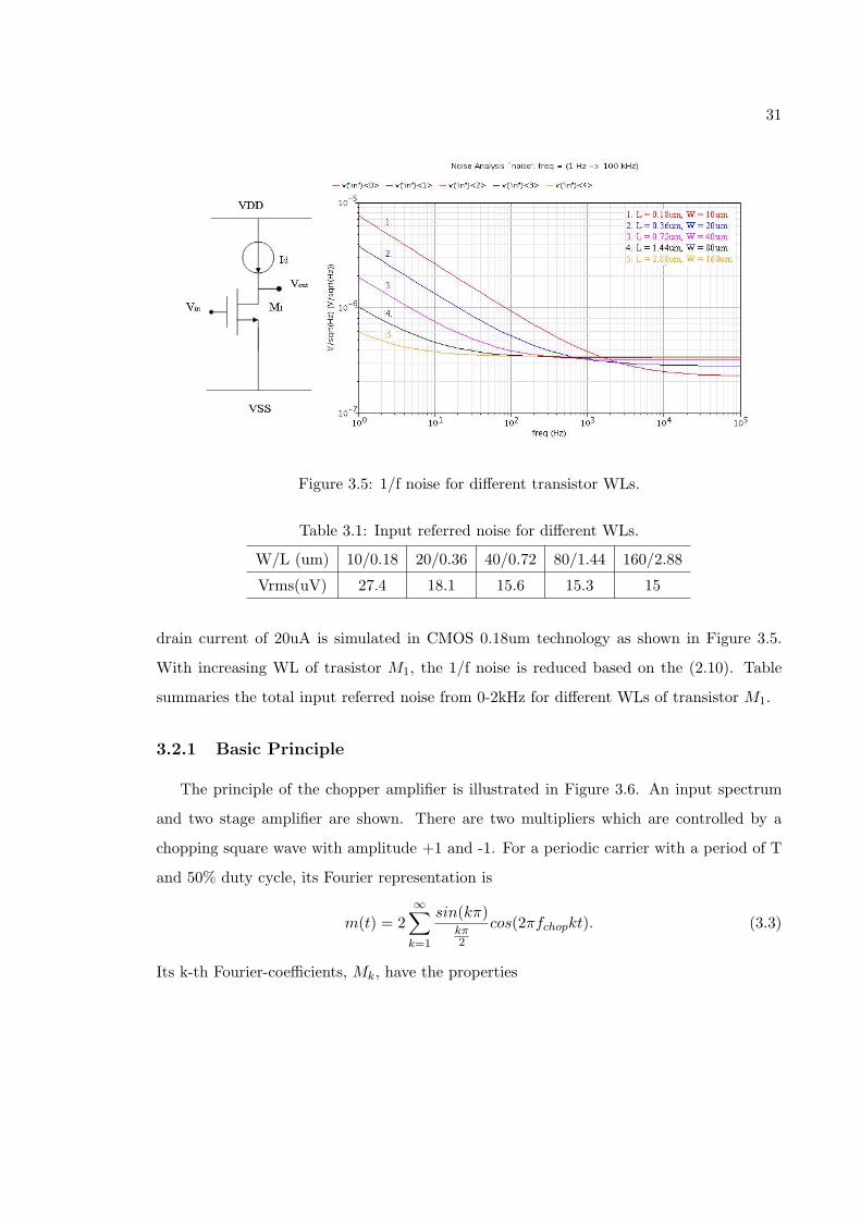
drain current of 20uA is simulated in CMOS 0.18um technology as shown in Figure 3.5.
With increasing WL of trasistor M1, the 1/f noise is reduced based on the (2.10). Table
summaries the total input referred noise from 0-2kHz for different WLs of transistor M1.
3.2.1 Basic Principle
The principle of the chopper amplifier is illustrated in Figure 3.6. An input spectrum
and two stage amplifier are shown. There are two multipliers which are controlled by a
chopping square wave with amplitude +1 and -1. For a periodic carrier with a period of T
and 50% duty cycle, its Fourier representation is
m(t) = 2∞∑k=1
sin(kπ)kπ2
cos(2πfchopkt). (3.3)
Its k-th Fourier-coefficients, Mk, have the properties
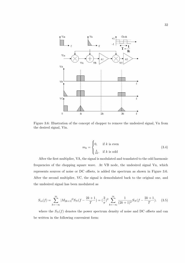
32
Figure 3.6: Illustration of the concept of chopper to remove the undesired signal, Vn fromthe desired signal, Vin.
mk =
0, if k is even
4πk , if k is odd
(3.4)
After the first multiplier, VA, the signal is modulated and translated to the odd harmonic
frequencies of the chopping square wave. At VB node, the undesired signal Vn, which
represents sources of noise or DC offsets, is added the spectrum as shown in Figure 3.6.
After the second multiplier, VC, the signal is demodulated back to the original one, and
the undesired signal has been modulated as
Scs(f) =∞∑
k=−∞|M2k+1|2SN (f − 2k + 1
T) = (
2
π)2
∞∑k=−∞
1
(2k + 1)2SN (f − 2k + 1
T). (3.5)
where the SN (f) denotes the power spectrum density of noise and DC offsets and can
be written in the following convenient form:

33
Figure 3.7: Circuit implementation for chopper technique in time domain.
SN = S0(1 +fCf). (3.6)
where S0 is the thermal in (2.9), and fC is the 1/f noise corner frequency in (2.12). As a
result, the spectrum of the undesired signal has been shifted to the odd harmonic frequencies
of the chopping square wave. If the chopper frequency fc is much greater than the signal
bandwidth, the undesired signal will be greatly reduced. Since the undesired signal signal
will contain 1/f noise and dc offsets of the amplifier, the influence of this source of undesired
signal is mixed out of the desired range of operation.
Another way to interpret the principle of chopper technique in time domain is shown
in Figure 3.7. The multipliers are implemented by two cross-coupled switches, which are
controlled by two nonoverlapping clocks ϕ1 and ϕ2. During ϕ1, the equivalent noise Veq is
equal to the input noise of the first stage plus that of the second divided by the gain of the
first stage. Thus, the equivalent noise at the input is given
Veq(ϕ1) = Vn1 +Vn2
A1. (3.7)
34
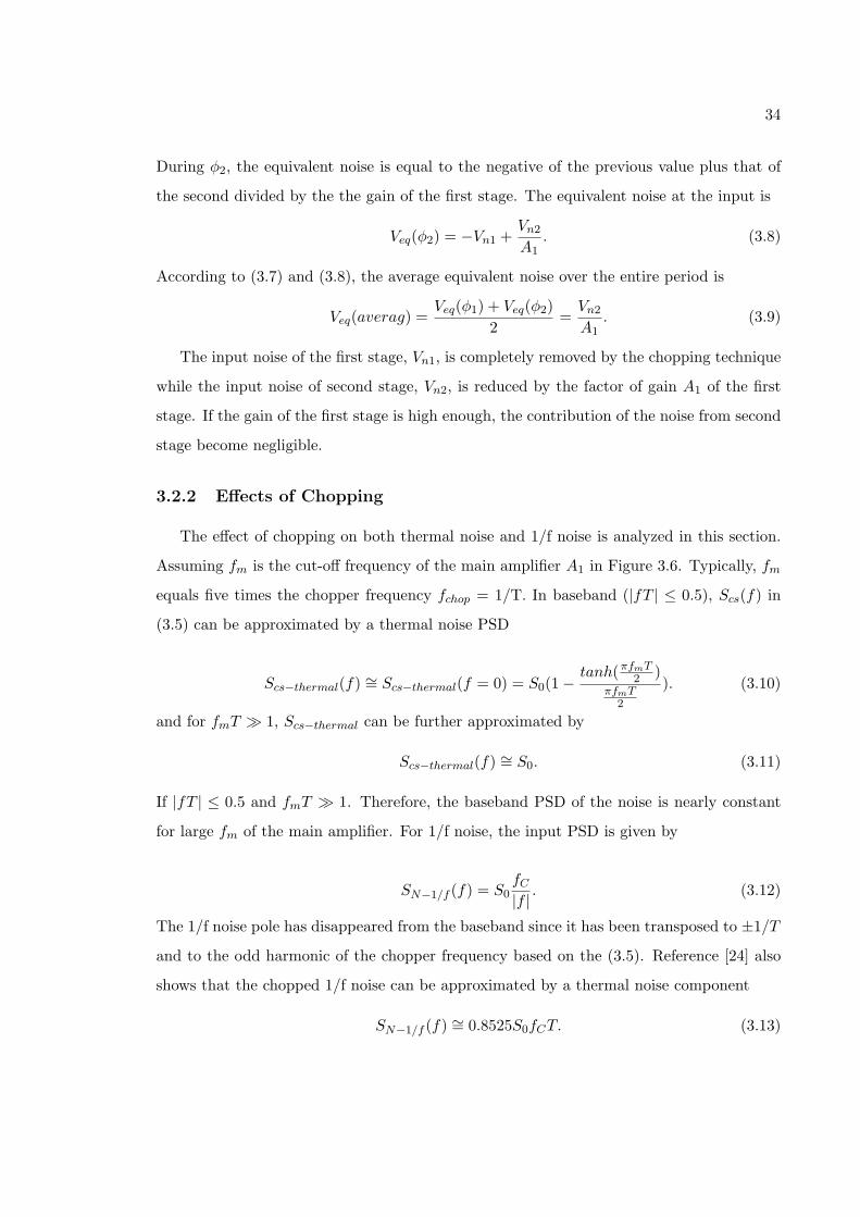
During ϕ2, the equivalent noise is equal to the negative of the previous value plus that of
the second divided by the the gain of the first stage. The equivalent noise at the input is
Veq(ϕ2) = −Vn1 +Vn2
A1. (3.8)
According to (3.7) and (3.8), the average equivalent noise over the entire period is
Veq(averag) =Veq(ϕ1) + Veq(ϕ2)
2=
Vn2
A1. (3.9)
The input noise of the first stage, Vn1, is completely removed by the chopping technique
while the input noise of second stage, Vn2, is reduced by the factor of gain A1 of the first
stage. If the gain of the first stage is high enough, the contribution of the noise from second
stage become negligible.
3.2.2 Effects of Chopping
The effect of chopping on both thermal noise and 1/f noise is analyzed in this section.
Assuming fm is the cut-off frequency of the main amplifier A1 in Figure 3.6. Typically, fm
equals five times the chopper frequency fchop = 1/T. In baseband (|fT | ≤ 0.5), Scs(f) in
(3.5) can be approximated by a thermal noise PSD
Scs−thermal(f) ∼= Scs−thermal(f = 0) = S0(1−tanh(πfmT
2 )πfmT
2
). (3.10)
and for fmT ≫ 1, Scs−thermal can be further approximated by
Scs−thermal(f) ∼= S0. (3.11)
If |fT | ≤ 0.5 and fmT ≫ 1. Therefore, the baseband PSD of the noise is nearly constant
for large fm of the main amplifier. For 1/f noise, the input PSD is given by
SN−1/f (f) = S0fC|f |
. (3.12)
The 1/f noise pole has disappeared from the baseband since it has been transposed to ±1/T
and to the odd harmonic of the chopper frequency based on the (3.5). Reference [24] also
shows that the chopped 1/f noise can be approximated by a thermal noise component
SN−1/f (f) ∼= 0.8525S0fCT. (3.13)
35
Figure 3.8: (a) Experimental chopper amplifier schematic. (OA1 and OA2 are CA3420and uA741 respectively, and the switches are MC14016.) (b) Observed input referred PSDwithout and with chopper.
The total noise in the baseband can be obtained by adding (3.11) and (3.13), resulting in
Scs(f) ∼= S0(1 + 0.8525S0fCT ). (3.14)
If the fT ≤ 0.5 and fCT ≫ 1. This has been verified experimentally on a breadboard
circuit with fchop=fC=1 KHz. The thermal noise without chopping was estimated to
be 37 nV/√
(Hz), and the theoretical thermal noise with chopping from (3.14) was 50.4
nV/√
(Hz) which is very close to the observed result shown in Figure 3.8.
3.2.3 Effect on Residual Offset
If the modulators are realized with MOS switches, then unwanted charges are injected
into the circuit when the transistors turn off. These non-idealities are charge injection and
clock feedthrough and cause residual offset (or spikes) at the input of the main amplifier.
This residual offset voltage will be amplified then demodulated by the output modulator. A

36
Figure 3.9: (a) Spike signal at the input signal and causing residual offset.(b) Spike signaland chopper-modulated spectra with amplifier bandwidth characteristics.
typical spike signal in time domain is shown in Figure 3.9. Figure 3.9(a) is the spike signal
at the input of the amplifier, and Figure 3.9(b) is the spike signal and input signal spectrum
in the frequency domain. τ is the time constant of parasitic spikes and T represents the
period of chopping. Since the τ is generally much small than T/2, most of spike appears
at frequencies higher than the chopping frequency. Assuming that the output modulator is
ideal, the output offset is given by [33]
Voffset,out = −∞∑
n=−∞
2
jπnj2πn
t0TA(
n
T)Vspike(
n
T) (3.15)
where t0 is a possible delay between the input and output modulation signals to compensate
for the phase shift introduced by the amplifier, n is odd based on (3.3), A is gain of amplifier
and
Vspike(f) = −∞∑
n=−∞δ(f − k
T)2τ
T
Vspike
1 + j2πfτ. (3.16)
is bilateral Fourier transform of the spike signal of Figure 3.9(a). The input referred offset
can be obtained assuming that τ ≪ T/1 and (3.15) reduces to:
Vos∼=
2τ
TVspike. (3.17)
where Vspike is the amplitude of the spikes at the chopper amplifier input as shown in
Figure 3.9(a). In the case of an ideal low-pass amplifier with gain A and a bandwidth
37
limited to 2fchop, the offset becomes
Vos∼= (
2τ
T)2Vspike. (3.18)
which is much smaller than that given by (3.17), since the τ has been assumed to be much
smaller than T/2. Therefore, the offset can be reduced drastically by limiting the bandwidth
of the amplifier to twice that chpooer frequency. Other techniques such as [25, 34–36] are
introduced to reduce the effect of spikes. Since the input offset can be reduce by limiting the
bandwidth of amplifier, the methods above are not used in this project. The non-idealities
of modulators are discussed in next chapter.
3.3 First Order Sigma-Delta ADC
Although the Σ∆ modulator was first introduced in 1962 [37], it did not gain attraction
until recent developments in digital VLSI technologies which provide the practical means
to implement the large digital signal processing circuitry. The increasing use of digital
techniques in communication and audio application has also contributed to the recent in-
terest in cost effective high precision A/D converters. A requirement of analog-to-digital
A/D interfaces is compatibility with VLSI technology, in order to provide for monolithic
integration of both the analog and digital sections on a single die. In this section , the first
order Σ∆ ADC in discrete and continuous time domains are reviewed respectively.
3.3.1 Discrete Time Implementation
Consider the first-order loop shown in Figure 3.10, the 1-bit quantizer is modeled as an
additive noise source. The Vout can be expressed as
V out(z) = z−1V out(z) + V in(z)− z−1D(z). (3.19)
and can be solved D(z) as
D(z) = V in(z) + (1− z−1)e(z). (3.20)
Based on the equation (3.20), the signal transfer function is
STF = 1. (3.21)

38
Figure 3.10: First order Σ∆ ADC in discrete time domain model
and noise transfer function is given by
NTF = (1− z−1). (3.22)
By setting z = ej2fπ, the squared magnitude of NTF in the frequency is given by
|NTF (ej2fπ)|2 = |2sin(πf)|2. (3.23)
where f is normalized frequency f/FS . For frequencies which satisfy f ≪ 1, |NTF |2 ≈
(2πf)2. Figure 3.11 illustrates the frequency response of the NTF. The quantization error
has been pushed towards high frequencies due to the (1− z−1) factor. Therefore the analog
input signal Vin(t) is oversampled, and the high-frequency quantization noise is removed
by digital LPF without affecting the input signal characteristics in baseband.
Based on the discussion on sections 2.2.1 and 3.1, the goal of SNR is completely deter-
mined by the thermal noise. However, it is necessary to find out the SNR for Σ∆ ADC in
order to meet the noise specification for overall system. The quantization noise power over
frequency band from 0 to f0 is given by
Pnoise =
∫ f0
0V 2Q(rms)|NTF (f)|2 df. (3.24)

39
0 0.1 0.2 0.3 0.4 0.50
0.5
1
1.5
2
2.5
3
3.5
4
Normalized Frequency (f/fs)
Figure 3.11: NTF plot for first order Σ∆ ADC
where the VQ(rms) is quantization error in (2.3), and the |NTF (f)|2 is noise transfer function
in (3.23). By making the approximation f0 ≪ FS , we have
Pnoise∼= (
VLSB
12)(π2
3)(2f0fs
) =V 2LSBπ
2
36(
1
OSR)3. (3.25)
where the over sampling rate OSR = FS/2f0. Assuming the signal power for a given
sinusoidal waveform with amplitude Vref in (2.5) is Vref/2√2, the SNR for this case is
given by
SNR = 10 log(Ps
Pnoise) = 10 log(
3
222N ) + 10 log(
3
π2(OSR)3). (3.26)
or, equivalently,
SNR = 6.02N + 1.76− 5.17 + 30 log(OSR). (3.27)
Equation (3.27) shows that the SNR increases by 9 dB for each doubling of the OSR.
The waveforms of Vin(t) and D(n) for a first-order Σ∆ modulator are illustrated in
Figure 3.12 when the input signal is a sinusoid with 0.5 V amplitude. In each clock cycle,
the value of the output of the modulator is either logic high or logic low, according to the
results of the 1-bit A/D conversion. When the sinusoidal input to the modulator is positive,
the output is also positive during most clock cycles. A similar statement holds for the case
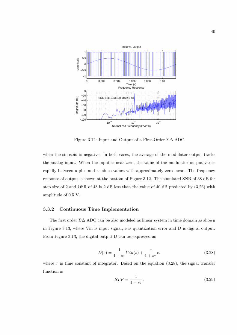
40
0 0.002 0.004 0.006 0.008 0.01
−1
−0.5
0
0.5
1
Time (s)
Mag
nitu
de
Input vs. Output
10−3
10−2
10−1
−120
−100
−80
−60
−40
−20
0
Normalized Frequency (Fs/2Fb)
Mag
nitu
de (
dB)
Frequency Response
SNR = 38.46dB @ OSR = 48
Figure 3.12: Input and Output of a First-Order Σ∆ ADC
when the sinusoid is negative. In both cases, the average of the modulator output tracks
the analog input. When the input is near zero, the value of the modulator output varies
rapidly between a plus and a minus values with approximately zero mean. The frequency
response of output is shown at the bottom of Figure 3.12. The simulated SNR of 38 dB for
step size of 2 and OSR of 48 is 2 dB less than the value of 40 dB predicted by (3.26) with
amplitude of 0.5 V.
3.3.2 Continuous Time Implementation
The first order Σ∆ ADC can be also modeled as linear system in time domain as shown
in Figure 3.13, where Vin is input signal, e is quantization error and D is digital output.
From Figure 3.13, the digital output D can be expressed as
D(s) =1
1 + sτV in(s) +
s
1 + sτe. (3.28)
where τ is time constant of integrator. Based on the equation (3.28), the signal transfer
function is
STF =1
1 + sτ. (3.29)

41
Figure 3.13: First order Σ∆ ADC in continuous time domain model
and noise transfer function is given by
NTF =sτ
1 + sτ. (3.30)
Figure 3.14 is the plot for signal and noise transfer functions. Notice that the signal and
noise transfer functions are LPF and HPF respectively. As we expected, the signal passes
the ADC while the quantization noise is pushed into high frequencies.
100
101
102
103
104
105
106
0.1
0.2
0.3
0.4
0.5
0.6
0.7
0.8
0.9
1
1.1NTFSTF
Figure 3.14: STF and NTF plot for first order Σ∆ ADC
42
Table 3.2: First order Σ∆ ADC operation for input signal = 1/3.
n 0 1 2 3 4 5 6
Vout(n) 1/3 -1/3 1 1/3 -1/3 1 1/3
D(n) 1 -1 1 1 -1 1 1
3.3.3 The Effects of Idle Tone
The periodic sequences generated by the DC inputs are introduced in this section. Con-
sider the behavior of first order Σ∆ ADC in Figure 3.10. From the block diagram, Vout(n)
is
V out(n) = V out(n− 1) + V in(n)−D(n− 1). (3.31)
and
D(n) = sgn(V out(n)). (3.32)
By combining the equations above,
V out(n) = V out(n− 1) + V in(n)− sgn(V out(n)). (3.33)
Now assume that the input signal Vin is 1/3, and also Vout(0) = 1/3. Then D(0) = 1,
Vout(1) = 1/3+0-1=-2/3 and D(1)=-1. The results of Vout and D are summarized in Table
3.2 for n=0 to 6. The average value of digital output D for a full period is (-1+1+1)/3=1/3,
which is identical to the input signal Vin. Thus, the output pattern is three cycles long and
its power is located at dc and FS/3.
Now consider applying a dc level of (1/3+1/9)=4/9 to the same modulator. For this
case, the output sequence becomes
D(n) = 1,−1, 1, 1, 1,−1, 1, 1,−1, 1, 1, 1,−1, 1, 1, 1,−1, 1, 1,−1, 1, .... (3.34)
The period of this output pattern is 16 cycles and has power at FS/16. The periodic
sequences generated by the dc input are sometimes called pattern noise, idle tones, or limit
cycles [38]. This amplitude does not change with time and its frequency and it depends
on the input. Based on the argument above, it is easy to find a tone at lower frequencies.
If a tone say FS/250 is inside band of interest, it could be a problem for next stage LPF
43
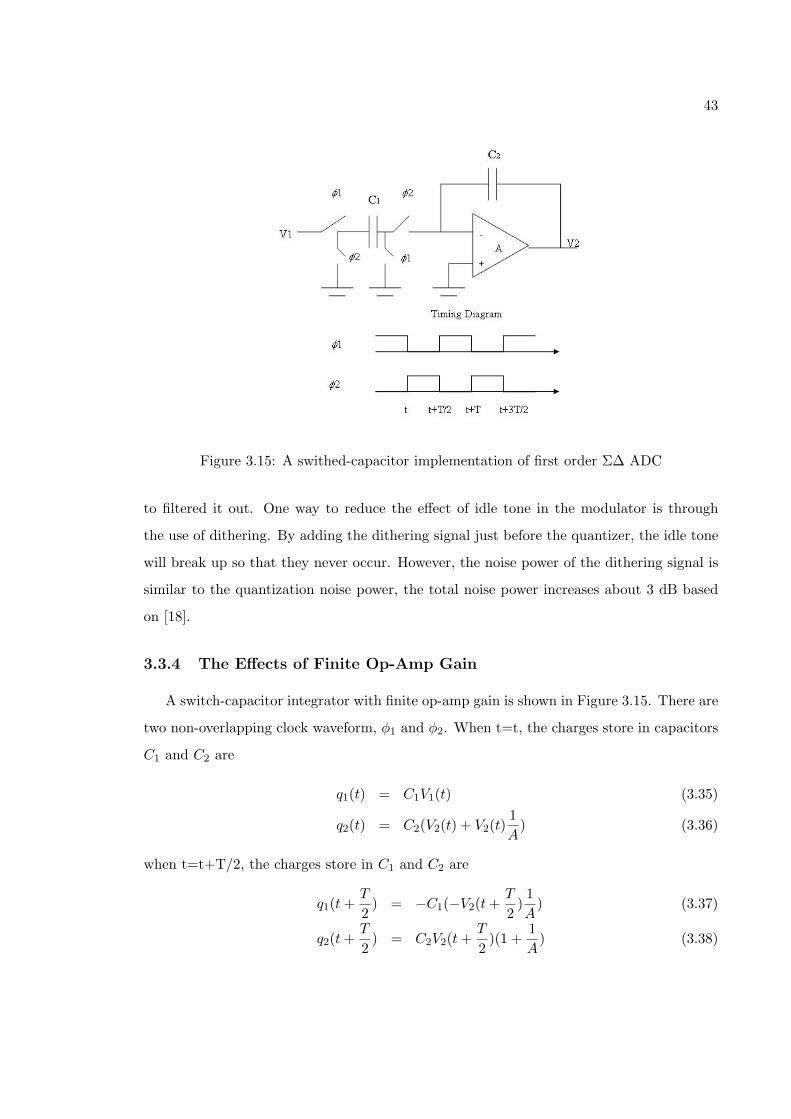
Figure 3.15: A swithed-capacitor implementation of first order Σ∆ ADC
to filtered it out. One way to reduce the effect of idle tone in the modulator is through
the use of dithering. By adding the dithering signal just before the quantizer, the idle tone
will break up so that they never occur. However, the noise power of the dithering signal is
similar to the quantization noise power, the total noise power increases about 3 dB based
on [18].
3.3.4 The Effects of Finite Op-Amp Gain
A switch-capacitor integrator with finite op-amp gain is shown in Figure 3.15. There are
two non-overlapping clock waveform, ϕ1 and ϕ2. When t=t, the charges store in capacitors
C1 and C2 are
q1(t) = C1V1(t) (3.35)
q2(t) = C2(V2(t) + V2(t)1
A) (3.36)
when t=t+T/2, the charges store in C1 and C2 are
q1(t+T
2) = −C1(−V2(t+
T
2)1
A) (3.37)
q2(t+T
2) = C2V2(t+
T
2)(1 +
1
A) (3.38)

44
Figure 3.16: Finite Op-Amp gain effect for NTF
By charge conservation, the total charges at t=t+T/2 are equal to those at t=t. Thus,
q2(t+T/2)+q1(t+T/2) = q1(t)+q2(t), and q2(t+T ) = q2(t+T/2) =⇒ V2(t+T/2) = V2(t).
Rearranging the equations above gives
C2V2(t+ T )(1 +1
A) = C1V1(t) + C2V2(t)(1 +
1
A)− C1V2(t+ T )
1
A
=⇒ C2V2(z)z(1 +1
A) = C1V1(z) + C2V2(z)(1 +
1
A)− C1V2(z)z
1
A
=⇒ C1V1(z) = V2(z)(C2z(1 +1
A)− C2(1 +
1
A)− C1z
1
A)
=⇒ H(z) =V2(z)
V1(z)
=C1
C2
1
z − 1
1+C1/C21+A
1
1 + (1 + C1C2
) 1A
(3.39)
As a result, the pole of the integrator moving to the left of z = 1 by an amount 1/A (If
C1∼= C2) as shown in Figure 3.16, and the gain is also changed according to (3.39). Thus,
the quantization noise does not drop to zero at dc but instead levels off near dc. If the
frequency band of interest, f0 is greater than 1/A rad/sample, any further doubling of the
oversampling ration will improve SNR. Finally, an approximation of minimum gian A is
givenf0FS
>1A
2π. (3.40)

45
since OSR = FS/2f0, the equation 3.40 can be rewrite as
A >OSR
π. (3.41)
According to [38], if the gain A is greater than OSR, the additional noise is less than 0.2
dB, and hence the effect is rarely serious.
3.3.5 The Effects of Timing Errors
Excess loop delay and clock jitter are two timing errors in Σ∆ modulators. These two
timing errors will be discussed in this section.
Excess Loop Delay
Ideally DAC currents respond immediately to the quantizers clock edge, but the non-
zero transistor switching time of the latched comparator (quantizer) and the DAC result
in a finite delay between the comparator and the DAC [39,40]. This delay is called Excess
Loop Delay shown in Figure 3.17. Assume the system is single-bit system with clock 1
MHz, and every 100 cycles the comparator output is delayed by td = 100ps. The average
power of equivalent error signal is
[2 tdT ]
100= 2× 10⁻⁶. (3.42)
which is 57 dB below the power of full-scale sine wave. Thus, the excess loop delay increases
the noise floor for a given Σ∆ modulator. The excess loop delay also potentially increases
the instability of the Σ∆ modulator by adding another order to the loop filter [41]. The
solutions to the excess loop delay are by adding extra feedback DAC as well as an adjustment
of the loop filter coefficients [38,39].
Clock jitter
There are two clocks in a Σ∆ modulator and both can be affected by clock jitter. One
of the clocks controls the decision instant of the quantizer while the other clock controls
the DAC output. Since the quantization error is pushed into high frequencies, the impact

46
Figure 3.17: Excess Loop Delay
of this error will be relatively small. Conversely, the output of the DAC is located in
band of interest, the impact of this error will affect the passband noise in the modulator.
The clock jitter in the DAC manifests itself as white noise. This degrades the SNR of
the Σ∆ modulator severely since the white noise spreads evenly across the band of interest.
Therefore the clock jitter discussed will be the pulse-width clock jitter incurred in the DAC.
DT Σ∆ modulator is insensitive to clock jitter due to the sloping pulse form of the
feedback. The clock jitter intruduces a relative small amount of error in charge lost ∆QD.
The capacitor is discharged over a fairly steep slop as shown at the left of Figure 3.18 [42].
In constrast, CT Σ∆ modulator transfers charge at a constant rate over the clock period,
and thus the charge loss ∆Qc due to timing error is much greater than that of DT Σ∆
Figure 3.18: Clock jitter

47
Figure 3.19: Σ∆ modulator with return to zero (RZ) and switched-capacitor-resistor (SRC)feedback
modulator shown at the right of Figure 3.18.
There are two solutions to reduce the effect of timing jitter in DAC. One of them is to
increase the number of levels in feedback DAC. Another solution to the jitter problem is to
change the feedback from a timing-dependent signal to a timing-insensitive signal.
Σ∆ modulator with return to zero (RZ) and switched-capacitor-resistor (SRC) feedback
is shown in Figure 3.19. Due to the sloping pulse form of the SCR feedback the white
noise power will be heavily reduced compared to the NRZ feedback [43]. The results for
both feedbacks are shown in Figure 3.20. The PSD of output is insensitive to rms jitter of
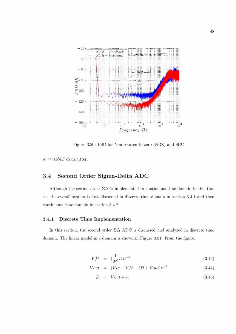
48
Figure 3.20: PSD for Non returen to zero (NRZ) and SRC
σt ∼= 0.5%T clock jitter.
3.4 Second Order Sigma-Delta ADC
Although the second order Σ∆ is implemented in continuous time domain in this the-
sis, the overall system is first discussed in discrete time domain in section 3.4.1 and then
continuous time domain in section 3.4.2.
3.4.1 Discrete Time Implementation
In this section, the second order Σ∆ ADC is discussed and analyzed in discrete time
domain. The linear model in z domain is shown in Figure 3.21. From the figure,
V fb = (1
2ND)z−1 (3.43)
V out = (V in− V fb− bD + V out)z−1 (3.44)
D = V out+ e. (3.45)
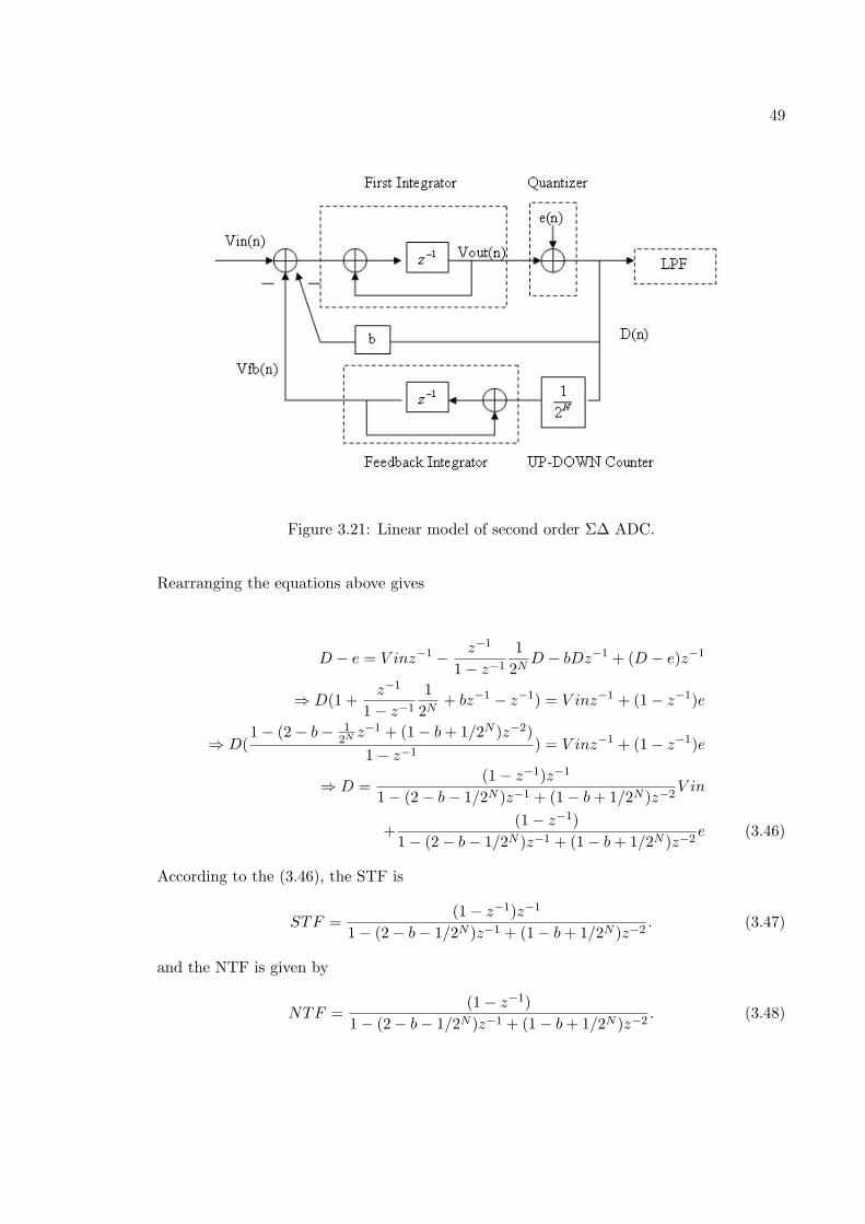
49
Figure 3.21: Linear model of second order Σ∆ ADC.
Rearranging the equations above gives
D − e = V inz−1 − z−1
1− z−1
1
2ND − bDz−1 + (D − e)z−1
⇒ D(1 +z−1
1− z−1
1
2N+ bz−1 − z−1) = V inz−1 + (1− z−1)e
⇒ D(1− (2− b− 1
2Nz−1 + (1− b+ 1/2N )z−2)
1− z−1) = V inz−1 + (1− z−1)e
⇒ D =(1− z−1)z−1
1− (2− b− 1/2N )z−1 + (1− b+ 1/2N )z−2V in
+(1− z−1)
1− (2− b− 1/2N )z−1 + (1− b+ 1/2N )z−2e (3.46)
According to the (3.46), the STF is
STF =(1− z−1)z−1
1− (2− b− 1/2N )z−1 + (1− b+ 1/2N )z−2. (3.47)
and the NTF is given by
NTF =(1− z−1)
1− (2− b− 1/2N )z−1 + (1− b+ 1/2N )z−2. (3.48)
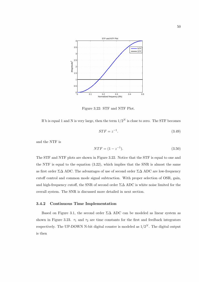
50
0 0.1 0.2 0.3 0.4 0.50
0.5
1
1.5
2
2.5
3
3.5
4
Normailzed frequency (f/fs)
|Mag
nitu
de|2
STF and NTF Plot
NTFSTF
Figure 3.22: STF and NTF Plot.
If b is equal 1 and N is very large, then the term 1/2N is close to zero. The STF becomes
STF = z−1. (3.49)
and the NTF is
NTF = (1− z−1). (3.50)
The STF and NTF plots are shown in Figure 3.22. Notice that the STF is equal to one and
the NTF is equal to the equation (3.22), which implies that the SNR is almost the same
as first order Σ∆ ADC. The advantages of use of second order Σ∆ ADC are low-frequency
cutoff control and common mode signal subtraction. With proper selection of OSR, gain,
and high-frequency cutoff, the SNR of second order Σ∆ ADC is white noise limited for the
overall system. The SNR is discussed more detailed in next section.
3.4.2 Continuous Time Implementation
Based on Figure 3.1, the second order Σ∆ ADC can be modeled as linear system as
shown in Figure 3.23. τ1 and τ2 are time constants for the first and feedback integrators
respectively. The UP-DOWN N-bit digital counter is modeled as 1/2N . The digital output
is then
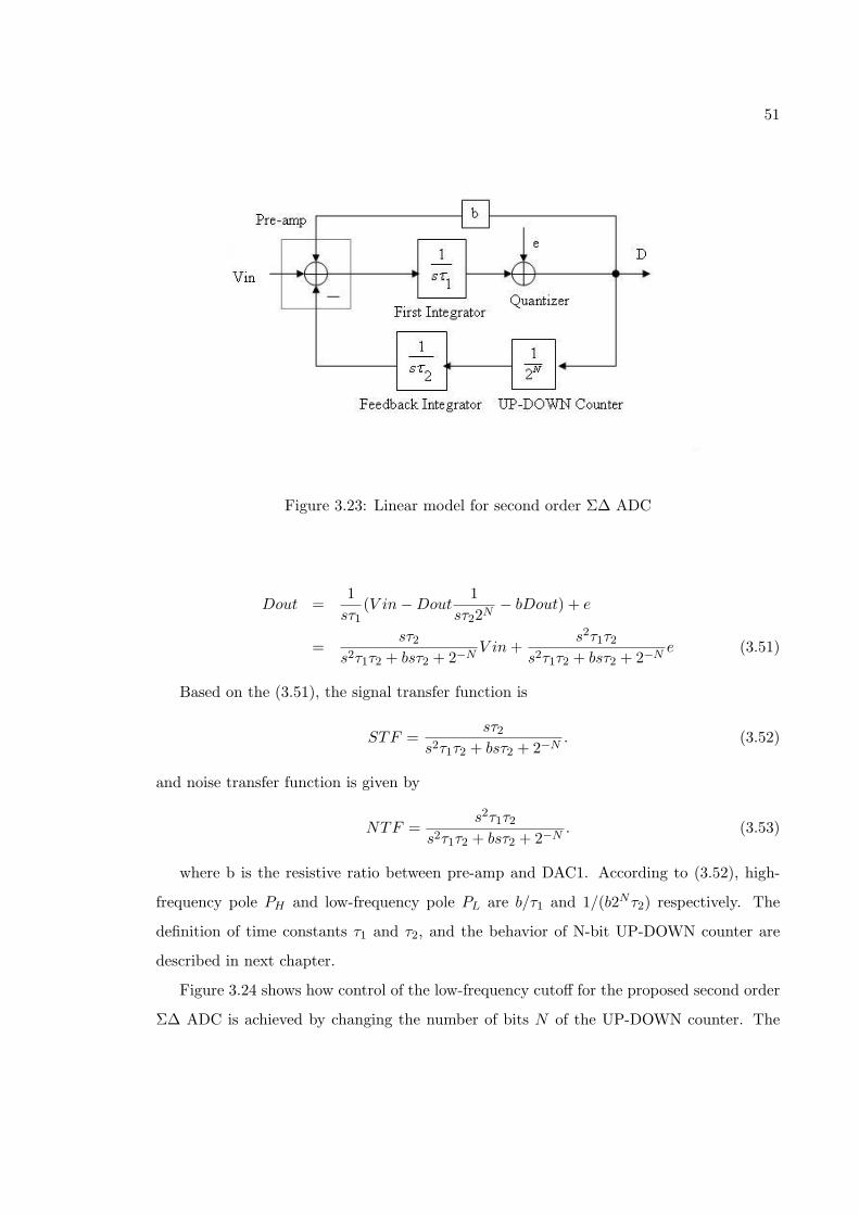
51
Figure 3.23: Linear model for second order Σ∆ ADC
Dout =1
sτ1(V in−Dout
1
sτ22N− bDout) + e
=sτ2
s2τ1τ2 + bsτ2 + 2−NV in+
s2τ1τ2s2τ1τ2 + bsτ2 + 2−N
e (3.51)
Based on the (3.51), the signal transfer function is
STF =sτ2
s2τ1τ2 + bsτ2 + 2−N. (3.52)
and noise transfer function is given by
NTF =s2τ1τ2
s2τ1τ2 + bsτ2 + 2−N. (3.53)
where b is the resistive ratio between pre-amp and DAC1. According to (3.52), high-
frequency pole PH and low-frequency pole PL are b/τ1 and 1/(b2Nτ2) respectively. The
definition of time constants τ1 and τ2, and the behavior of N-bit UP-DOWN counter are
described in next chapter.
Figure 3.24 shows how control of the low-frequency cutoff for the proposed second order
Σ∆ ADC is achieved by changing the number of bits N of the UP-DOWN counter. The
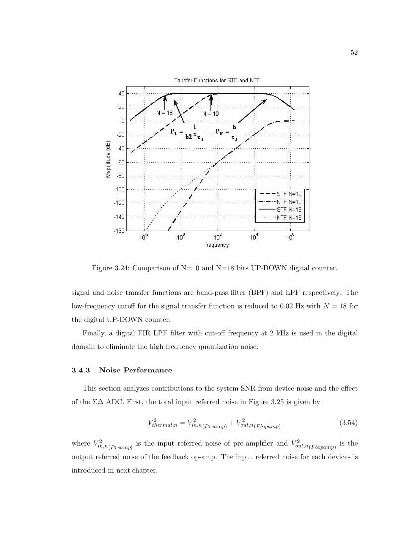
52
Figure 3.24: Comparison of N=10 and N=18 bits UP-DOWN digital counter.
signal and noise transfer functions are band-pass filter (BPF) and LPF respectively. The
low-frequency cutoff for the signal transfer function is reduced to 0.02 Hz with N = 18 for
the digital UP-DOWN counter.
Finally, a digital FIR LPF filter with cut-off frequency at 2 kHz is used in the digital
domain to eliminate the high frequency quantization noise.
3.4.3 Noise Performance
This section analyzes contributions to the system SNR from device noise and the effect
of the Σ∆ ADC. First, the total input referred noise in Figure 3.25 is given by
V 2thermal,n = V 2
in,n(Preamp)+ V 2
out,n(Fbopamp)(3.54)
where V 2in,n(Preamp)
is the input referred noise of pre-amplifier and V 2out,n(Fbopamp)
is the
output referred noise of the feedback op-amp. The input referred noise for each devices is
introduced in next chapter.
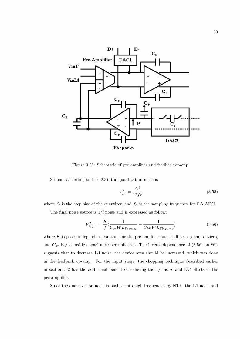
53
Figure 3.25: Schematic of pre-amplifier and feedback opamp.
Second, according to the (2.3), the quantization noise is
V 2q,n =
2
12fS(3.55)
where is the step size of the quantizer, and fS is the sampling frequency for Σ∆ ADC.
The final noise source is 1/f noise and is expressed as follow:
V 21/f,n =
K
f(
1
CoxWLPreamp+
1
CoxWLFbopamp) (3.56)
where K is process-dependent constant for the pre-amplifier and feedback op-amp devices,
and Cox is gate oxide capacitance per unit area. The inverse dependence of (3.56) on WL
suggests that to decrease 1/f noise, the device area should be increased, which was done
in the feedback op-amp. For the input stage, the chopping technique described earlier
in section 3.2 has the additional benefit of reducing the 1/f noise and DC offsets of the
pre-amplifier.
Since the quantization noise is pushed into high frequencies by NTF, the 1/f noise and
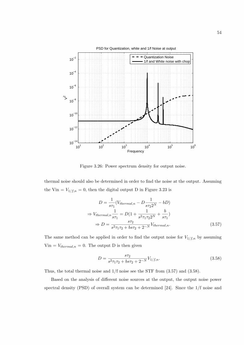
54
101
102
103
104
105
106
10−14
10−12
10−10
10−8
10−6
10−4
10−2
Frequency
V2
PSD for Quantization, white and 1/f Noise at output
Quantization Noise1/f and White noise with chop
Figure 3.26: Power spectrum density for output noise.
thermal noise should also be determined in order to find the noise at the output. Assuming
the Vin = V1/f,n = 0, then the digital output D in Figure 3.23 is
D =1
sτ1(Vthermal,n −D
1
sτ22N− bD)
⇒ Vthermal,n1
sτ1= D(1 +
1
s2τ1τ22N+
b
sτ1)
⇒ D =sτ2
s2τ1τ2 + bsτ2 + 2−NVthermal,n. (3.57)
The same method can be applied in order to find the output noise for V1/f,n by assuming
Vin = Vthermal,n = 0. The output D is then given
D =sτ2
s2τ1τ2 + bsτ2 + 2−NV1/f,n. (3.58)
Thus, the total thermal noise and 1/f noise see the STF from (3.57) and (3.58).
Based on the analysis of different noise sources at the output, the output noise power
spectral density (PSD) of overall system can be determined [24]. Since the 1/f noise and

55
DC offsets at the input are only modulated by the output chopper, the output PSD in (3.5)
can be expressed by
Sout,thernal(f) = (2
π)2
∞∑n=−∞
1
n2Sin,w(f − nfchop)|STF (f)|2 (3.59)
where n is an odd number, fchop is chopping frequency, and Sin is V 2thermal,n in (3.54). The
output PSD for quantization noise is given by
Sout,q = Vq,n|NTF (f)|2 (3.60)
Figure 3.26 shows the total output PSD for each noise source with chopping frequency
at 10 kHz with total thermal noise 1uVrms, and OSR = 250. Notice that the 1/f noise has
been removed by chopping technique. The intersection between PSD for quantization noise
and white noise is above 2 kHz. This implies that SNR is white noise limited, and the SNR
will not improve with higher order Σ∆ ADC design. Achieving higher SNR would require
lower white noise and an associated increase in power dissipation.
3.4.4 Common Mode Subtraction
With differential pairs in the front-end, the input common mode range to preserve
adequate linearity is only a few millivolts. Several techniques are used in order to improve
linearity [29,30,44,45]. However, the increased noise from adding extra devices in the front-
end is an issue. In Figure 3.1, the complementary Gm stage provides a wide input common
mode range such that the common mode DC offsets due to skin-electrode interface can be
subtracted by the pre-amplifier. The circuit implementation of Gm is described in next
chapter.
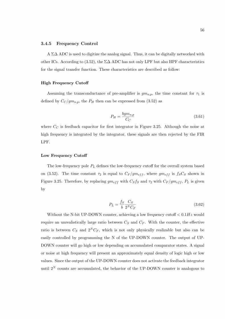
56
3.4.5 Frequency Control
A Σ∆ ADC is used to digitize the analog signal. Thus, it can be digitally networked with
other ICs. According to (3.52), the Σ∆ ADC has not only LPF but also HPF characteristics
for the signal transfer function. These characteristics are described as follow:
High Frequency Cutoff
Assuming the transconductance of pre-amplifier is gmn,p, the time constant for τ1 is
defined by CC/gmn,p, the PH then can be expressed from (3.52) as
PH =bgmn,p
CC(3.61)
where CC is feedback capacitor for first integrator in Figure 3.25. Although the noise at
high frequency is integrated by the integrator, these signals are then rejected by the FIR
LPF.
Low Frequency Cutoff
The low-frequency pole PL defines the low-frequency cutoff for the overall system based
on (3.52). The time constant τ2 is equal to CF /gmeff , where gmeff is fSCS shown in
Figure 3.25. Therefore, by replacing gmeff with CSfS and τ2 with CF /gmeff , PL is given
by
PL =fSb
CS
2NCF(3.62)
Without the N-bit UP-DOWN counter, achieving a low frequency cutoff < 0.1Hz would
require an unrealistically large ratio between CS and CF . With the counter, the effective
ratio is between CS and 2NCF , which is not only physically realizable but also can be
easily controlled by programming the N of the UP-DOWN counter. The output of UP-
DOWN counter will go high or low depending on accumulated comparator states. A signal
or noise at high frequency will present an approximately equal density of logic high or low
values. Since the output of the UP-DOWN counter does not activate the feedback integrator
until 2N counts are accumulated, the behavior of the UP-DOWN counter is analogous to
57
a lowpass characteristic in the feedback path. The input subtracts the lowpass feedback,
resulting in a highpass characteristic for the overall system transfer function.
3.5 Summary for Overall System
A novel second order Σ∆ ADC with feedback integrator from the Σ∆ output is pre-
sented. With feedback integrator and UP-DOWN counter, the low-frequency cutoff can
be programmed. In addition, the Gm stage enables the wide input common mode while
the common mode signal at the input is subtracted by the pre-amplifier. The SNR is
dominated by the thermal noise as discussed in section 3.4.3. In next chapter, the circuit
implementation for each block is described and discussed.

58
Chapter 4
Circuit Implementation of
Sigma-Delta ADC
The second order Σ∆ ADC outlined in Chapter 3 is implemented in Jazz Semiconductor
0.18 um CMOS technology . In section 4.1, a detailed description of pre-amplifier, op-amp,
DAC1, and chopping block are discussed. In section 4.2, the implementation of op-amp for
second integrator is presented. The design of UP-DOWN counter, DAC2, and GM stage
are also described. In section 4.3, the quantizer are presented, followed by a simulation
results of the actual chip layout in section 4.4.
Figure 4.1: First integrator.

59
Figure 4.2: Circuit implementation of pre-amplifier.
4.1 First Integrator
The first order integrator of overall system is in Figure 4.1. The circuit implementation
of pre-amplifier, chopping block, op-amp, and DAC1 are discussed in this section.
4.1.1 Pre-Amplifier
Figure 4.2 shows the pre-amplifier, which is designed with complementary NMOS-PMOS
differential pairs. The input differential voltages are converted to a current as
Iout = gmp(VinP − VinM )− gmn(VfbP − VfbM ) (4.1)
where VinP ,VinM and VfbP , VfbM are input signals from electrodes and signals from feed-
back integrator respectively, and gmn and gmp are transconductance of NMOS and PMOS

60
differential pairs. The current Iout is then integrated in continuous time by the first inte-
grator.
Mismatch between NMOS and PMOS differential pairs would cause linearity errors for
the differential signal. Also, the pre-amplifier must provide equal and opposite gains in each
path to implement subtraction of the common interference (4.1). As shown in Figure 4.1,
chopping technique is used to modulate the effects of these mismatch errors to high fre-
quency where they can be removed by the FIR LPF. For low noise pre-amplifier design [4],
the drain current and sizing of each transistor are implemented with transconductance gmn,p
of 630µA/V as shown in Figure 4.2.
Although the circuit topology is a standard design suitable for driving capacitive loads,
the sizing of transistors is critical for achieving low noise at low current levels. The bias
current is set to 60 uA, giving devices M1 to M4 drain currents of 30 uA. At this current
level, each transistor may operate in weak, moderate, or strong inversion depending on
its W/L ratio. For low noise pre-amplifier design, each transistor is operated in moderate
region and its moderate inversion characteristic current IS [19] is given by
IS =2uCoxV
2T
κ
W
L(4.2)
where VT is the thermal voltage kT/q, and κ is the subthreshold gate coupling coefficient.
Note that κ has typical value of 0.7.
The inversion coefficient (i) is
i =IDIS
(4.3)
For large currents (i>10), the transistor operates in strong inversion. For very small
currents (i<0.1), the transistor is in the weak inversion. The region between (0.1<i<10) is
called the moderate inversion region as shown in Figure 4.3. It provides a smooth transition
between two regions. Figure 4.3 also shows the relationship between the over drive voltage
VGS − Vth of MOS transistor and its inversion coefficient i. The EKV model [19] is used in
order to calculate transconductance gm, the gm is given by
gm1−4 =κIDVT
2
1 +√1 + 4i
(4.4)

61
Figure 4.3: Relation between VGS − Vth and inversion coefficients i.
Table 4.1: Operating Point of Pre-Amplifier
Devices ID(uA) gm/ID(V−1) Vgs − Vth(mV )
M1,M2 30 21 42
M3,M4 30 21 46
Table 4.1 summaries the operating conditions of each transistor. Based on Figure 4.3,
the VGS − Vth for both NMOS and PMOS differential pairs are closed to 50 mV which are
located inside the moderate region.
Input referred noise
According to Figure 4.2, the total input referred noise can be found by
V 2in,n(total)
=8
3
kT
gm1−4+
K
f(
1
CoxWLM1−4
) (4.5)
where the first term is thermal noise, and last term is 1/f noise. Since the 1/f noise is
modulated into high frequencies by the output modulator, the total input referred noise is
then dominated by the thermal noise. The total thermal noise is 8.4nV/√Hz based on gm
of 630uA/V .

62
In order to compare the noise specification with other works, a noise efficiency factor is
introduced by [46]
NEF = Vin,rms
√2Itotal
πVT 4kTBW. (4.6)
where the Vin,rms is input referred noise rms noise voltage, Itotal is the total current of
pre-amplifier, and BW is bandwidth of pre-amplifier in hertz. An amplifier using a BJT
transistor has
NEF =
√2kT
gm
π
2BW
2ItotalπVT 4kTBW
=
√1
2
= 0.707. (4.7)
Any practical circuits have higher value of NEF. Integrating the expression (4.5) over band-
width BW and substituting into (4.6), the noise efficiency factor is
10−2
10−1
100
101
10−1
100
101
102
103
104
Input−Referred Noise /Root (Bandwidth) [u Vrms / Hz1/2 ]
Sup
ply
Cur
rent
[uA
]
This Work
AD 620
[6]
[8]
[3] [17]
[1][2]
[9]
[18] [41]
NEF = 1NEF = 10
NEF = 100
Figure 4.4: Supply Current versus normalized noise for amplifiers. Dash lines indicateconstant NEF contours.

63
NEF =
√8kT
3gm1−44π
2BW
2ItotalπVT 4kTBW
=
√8Itotal
3VT gm1−4
=
√16ID1
3VT gm1−4
(4.8)
Based on Table 4.1, the NEF is equal to 3.1.
Figure 4.4 shows the power-noise performance of pre-amplifier compared with esti-
mated NEF values based on equation (4.6) from previous published bio-amplifiers. The
pre-amplifier has better NEF than existing designs.
4.1.2 Chopping Block
The Chopping technique is used to modulated the dc offsets and 1/f noise of amplifier
stage to the odd harmonic frequencies of the chopping square signal FC . The implementation
of chopping block is shown in Figure 3.7. However, the MOS switch nonidealities include a
nonzero and nonlinear on-resistor as discussed in section 3.2.3. The factors affecting residual
offset are as follow:
• clock feedthrough;
• charge injection;
• sampled noise;
• leakage current.
The nonlinear effects of MOS transistor can be reduced by circuit techniques. The
techniques are
• complementary switches;
• dummy transistor;
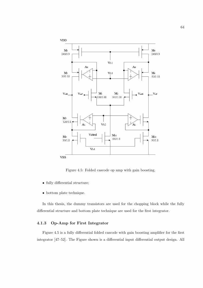
64
Figure 4.5: Folded cascode op amp with gain boosting.
• fully differential structure;
• bottom plate technique.
In this thesis, the dummy transistors are used for the chopping block while the fully
differential structure and bottom plate technique are used for the first integrator.
4.1.3 Op-Amp for First Integrator
Figure 4.5 is a fully differential folded cascode with gain boosting amplifier for the first
integrator [47–52]. The Figure shown is a differential input differential output design. All
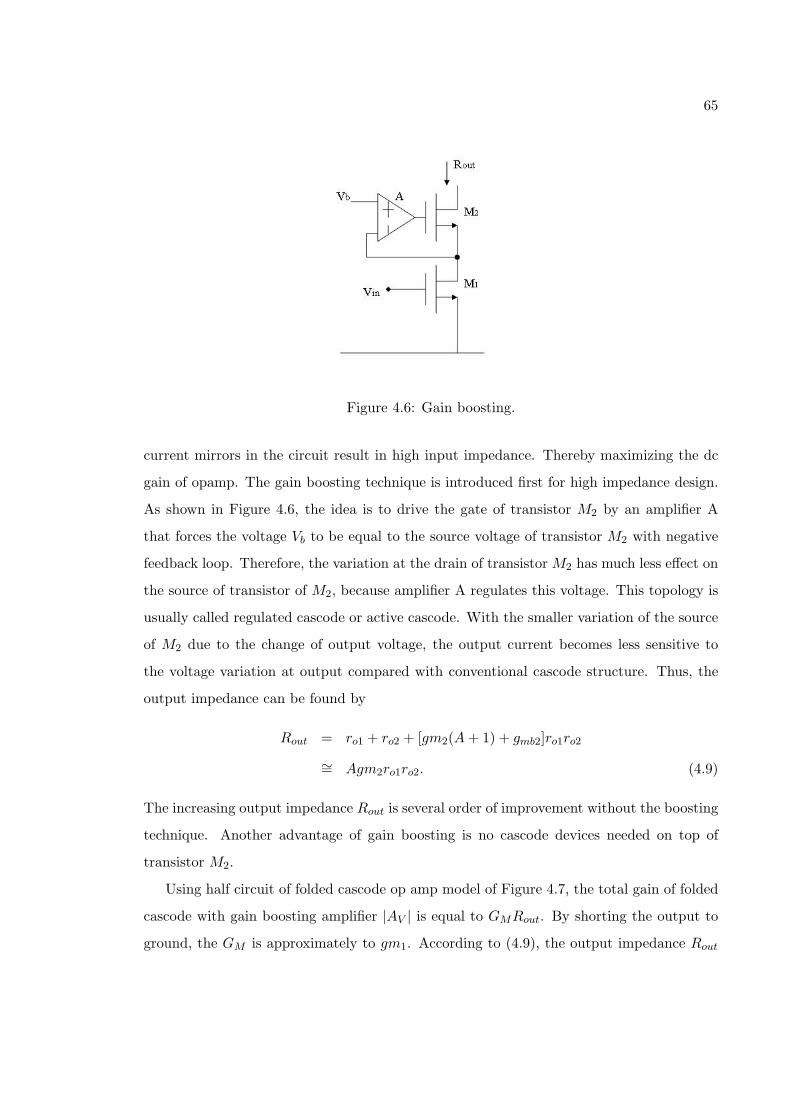
65
Figure 4.6: Gain boosting.
current mirrors in the circuit result in high input impedance. Thereby maximizing the dc
gain of opamp. The gain boosting technique is introduced first for high impedance design.
As shown in Figure 4.6, the idea is to drive the gate of transistor M2 by an amplifier A
that forces the voltage Vb to be equal to the source voltage of transistor M2 with negative
feedback loop. Therefore, the variation at the drain of transistor M2 has much less effect on
the source of transistor of M2, because amplifier A regulates this voltage. This topology is
usually called regulated cascode or active cascode. With the smaller variation of the source
of M2 due to the change of output voltage, the output current becomes less sensitive to
the voltage variation at output compared with conventional cascode structure. Thus, the
output impedance can be found by
Rout = ro1 + ro2 + [gm2(A+ 1) + gmb2]ro1ro2
∼= Agm2ro1ro2. (4.9)
The increasing output impedance Rout is several order of improvement without the boosting
technique. Another advantage of gain boosting is no cascode devices needed on top of
transistor M2.
Using half circuit of folded cascode op amp model of Figure 4.7, the total gain of folded
cascode with gain boosting amplifier |AV | is equal to GMRout. By shorting the output to
ground, the GM is approximately to gm1. According to (4.9), the output impedance Rout
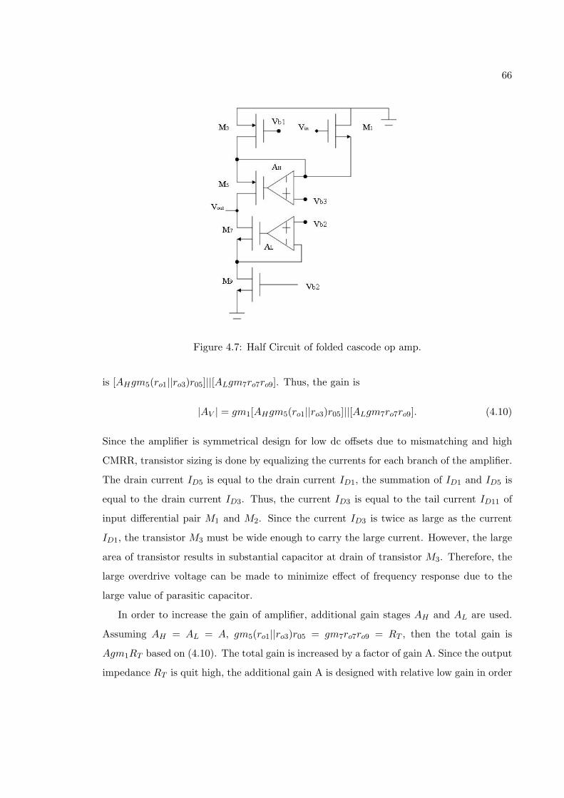
66
Figure 4.7: Half Circuit of folded cascode op amp.
is [AHgm5(ro1||ro3)r05]||[ALgm7ro7ro9]. Thus, the gain is
|AV | = gm1[AHgm5(ro1||ro3)r05]||[ALgm7ro7ro9]. (4.10)
Since the amplifier is symmetrical design for low dc offsets due to mismatching and high
CMRR, transistor sizing is done by equalizing the currents for each branch of the amplifier.
The drain current ID5 is equal to the drain current ID1, the summation of ID1 and ID5 is
equal to the drain current ID3. Thus, the current ID3 is equal to the tail current ID11 of
input differential pair M1 and M2. Since the current ID3 is twice as large as the current
ID1, the transistor M3 must be wide enough to carry the large current. However, the large
area of transistor results in substantial capacitor at drain of transistor M3. Therefore, the
large overdrive voltage can be made to minimize effect of frequency response due to the
large value of parasitic capacitor.
In order to increase the gain of amplifier, additional gain stages AH and AL are used.
Assuming AH = AL = A, gm5(ro1||ro3)r05 = gm7ro7ro9 = RT , then the total gain is
Agm1RT based on (4.10). The total gain is increased by a factor of gain A. Since the output
impedance RT is quit high, the additional gain A is designed with relative low gain in order

67
to save the power and die area. Figures 4.8 and 4.9 are additional gain stages AH and AL
to boost the output impedance of PMOS and NMOS current sources respectively. The AH
and AL consist of one differential pair and three current mirrors. The input differential
pairs M1−2 are loaded with two equal current mirrors M3−4, which provide a current gain
B to the output. The current gain B can be found by the ratio between W5/W3. The total
Figure 4.8: Additional Gian stage for boosting output impedance of PMOS current sources.
Figure 4.9: Additional Gian stage for boosting output impedance of NMOS current sources.

68
Figure 4.10: A conceptual block diagram of the CMFB loop.
gain of AH and AL are then determined by the ratio Bgm1,2/gm3,4.
Common Mode Feed Back (CMFB) circuit for OP-Amp
Since the amplifier is designed with fully differential topology, the output voltages are
not well defined compare to the single-end amplifier. Therefore, the common mode feedback
(CMFB) circuitry is needed in order to set the common mode output voltage correctly as
shown in Figure 4.10 [53]. The purpose of CMFB is to sense the common mode voltage,
Voc, by the CM detector then to compare with a reference voltage, VCM . If the Voc is higher
than the VCM , the bias current ID11 is increased in order to bring the Voc down until both
of VCM and Voc agree. A similar statement holds for the case when the Voc is lower than
the VCM .
The small-signal model can be also analyzed based on Figure 4.10. The CMFB loop
uses negative feedback to make Voc∼= VCM , the Voc can be expressed as
Voc = AcmsAcmc(Voc − VCM ). (4.11)

69
Thus, the ratio Voc/VCM is the closed-loop small-signal gain of the CMFB, which is
ACMFB =∆Voc
∆VCM
=Voc
VCM
=Acms(−Acmc)
1 +Acms(−Acmc). (4.12)
where the Acms the gain of CMFB, and the Acmc is the gain from Vctrol to Voc. The gain of
Acmc can be obtained by applying the input to the gate of transistor M11, and is given by
|Acmc| = gm11H [AHgm5(gm1ro1ro11||ro3)r05]||[ALgm7ro7ro9]. (4.13)
where gm11H is equal to gm11/2 in CM half-circuit. Since Acms(−Acmc) is much greater
than one, ACMFB ≈ 1 and ∆Voc ≃ ∆VCM . If the VCM changes by a small amount, Voc
should change by an equal amount so that Voc tracks VCM .
Since the CMFB loop is a negative feedback loop, it is important to check the loop is
stable or not. The dominant pole Pcp in the CMFB is set by the load capacitance CL and
the output impedance in the CM half-circuit. The Acmc(s) is
Acmc(s) = −gm11H [AHgm5(gm1ro1ro11||ro3)r05]||[ALgm7ro7ro9]
1 + s(AHgm5(gm1ro1ro11||ro3)r05)CL. (4.14)
At high frequency w ≫ Pcp, (4.14) reduces to
Acmc(s) = −gm11H
sCL. (4.15)
The unity frequency of CMFB is gm11H/CL. For stability issue, the adequate phase
margin for CMFB can be designed by splitting the transistor M11 into two identical devices.
Thus, gm11H = gm11/2 decreases gain of Acmc and therefore increases the phase margin of
CMFB loop. For high speed application, the gain-bandwidth-product (GBW) of common
mode is designed to be higher than the differential GBW gm1/CL. Therefore, the fast
common-mode feedback would not take much time to restore the biasing in the input stage.
In this case, the tradeoffs between power and speed are challenges for circuit design.
Figure 4.11 is a CMFB circuitry in continuous time domain. The source-coupled pairs
M1−2 and M3−4 together sense the common mode output voltages and generate an output

70
Figure 4.11: A continuous-time CMFB circuit.
that is proportional to the difference between Voc and VCM . Assume VOP − VCM and
VOM − VCM are small, drain currents of transistor M7 and M8 are equal to I, and the
common mode gain of CMFB is zero. Under these assumptions, the drain currents in M2
and M3 are
Id2 = −I
2− gm2
VOP − VCM
2. (4.16)
Id3 = −I
2− gm3
VOM − VCM
2. (4.17)
The two currents are summed in diode-connected transistor M6 to give the common mode
output current
Id6 = −Id2 − Id3
= I + gm2(VOP + VOM
2− VCM )
= I + gm2(Voc − VCM ). (4.18)
where gm2 = gm3 is assumed. This shows that the current includes a dc term I and a term

71
that is proportional to Voc − VCM . The current Id6 is mirrored by M11 in Figure 4.5 to
produce the tail current in the amplifier, which controls the common mode output voltage.
A modified version of the CMFB can be made by splitting the transistor M6 into two
equal size transistors. One of these transistors is diode-connected and tie the gate to Vctrol,
and the other one is biased at a constant current which is equal to I. This changes effectively
doubles the common mode gain of the circuit with very good linearity [54].
Noise Analysis
The noise performance of op amp is analyzed in this section. Since the noise of active
cascode devices is negligible at low frequency, the total output noise is contributed by
transistors M1−2, M3−4, and M9−10. To determine the input-referred thermal noise, the
noise sources of M3−4 are referred to the output:
Vn,out = 2(4kT2
3gm3,4gm2
3,4R2out). (4.19)
where the factor 2 accounts for noise of M3 and M4, and Rout is the open-loop output
impedance of the op amp. Similarly, for transistors M9 and M10
Vn,out = 2(4kT2
3gm9,10gm2
9,10R2out). (4.20)
Dividing (4.19) and (4.20) by gm21,2R
2out and adding the contribution of M1−2, the total
input referred noise is
Vn,in = 8kT (2
3gm1,2+
2
3
gm3,4
gm21,2
+2
3
gm9,10
gm21,2
). (4.21)
According the equation above, the gm1,2 can be made larger in order to reduce the noise
at the input. However, the noise contribution from transistors M3,4 have effect on the noise
performance because the currents Id3,d4 are twice as large as current Id1. The simulation
result of total input referred noise is shown in the end of this chapter.
Frequency and Transient Response
The settling time is an important parameter of amplifier for use in applications such
as A/D and D/A. The settling time consists of two distinct periods. The first portion is

72
slew-rate (SR) limit, and it acts nonlinear fashion. The time of slew-rate is determined by
the current to charge the amplifier compensation capacitor. With a load or compensation
capacitor CL, the slew-rate may limit by a fixed biasing current. Thus, the linear settling
time will be affected by the slew-rate in this case. Increasing biasing current is one way
to avoid the slew-rate limiting. However, the power consumption is increased with fast
settling time. Another way to improve the SR is to reduce the transconductance of gm1,2
while keeping the bias current constant. It will lower the dc gain and increase the noise [53].
The second portion of settling time is due to the finite unity-gain frequency (wt) of the
amplifier and it acts in a linear fashion. Several work have been shown that this period is
significantly affected by the presence of pole-zero pairs in the amplifier with gain boosting
design [48, 55, 56]. A solution is provided to avoid the effect of pole-zero doublet by the
additional gain stage in this section.
A model which represents the behavior for slewing of input differential pair of amplifier
and transient response is shown in Figure 4.12. The differential input stage is modeled
as shown with maximum current IO and voltage Vx is limited by Io/gm. For the voltage
|Vx| > Io/gm, the input stage is limited by a current Io. This is nonlinearity behavior
in the transient response. A pole-zero doublet is also modeled between the input stage
and single-pole stage. The settling time behavior between slewing and pole-zero effects are
discussed next.
Settling Time and Slew Rate (SR) Limit
For settling time requirement, If the amplifier needs to settle within 1/2 LSB at the 16
bit level in 24 nsec. With feedback β ∼= 1, we can obtain,
1
217= e
−24nsτ
⇒ τ ∼= 2ns. (4.22)
Since τ = 1/βwt, wt is equal to 87.5 MHz. From wt = gm/CL, the gm is 1.6mA/V . The
bias current ID11 is 164 uA by using the square-law relationship gm = 2ID/Veff . Where
the effective over dirve voltage is assumed to be 0.2V . Based on the bias current ID11, the
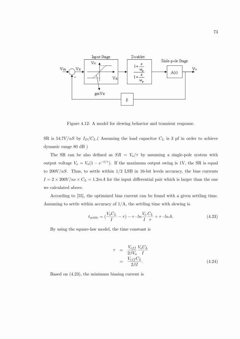
73
Figure 4.12: A model for slewing behavior and transient response.
SR is 54.7V/uS by ID/CL.( Assuming the load capacitor CL is 3 pf in order to achieve
dynamic range 80 dB )
The SR can be also defined as SR = Vo/τ by assuming a single-pole system with
output voltage Vo = Vo(1 − e−t/τ ). If the maximum output swing is 1V, the SR is equal
to 200V/uS. Thus, to settle within 1/2 LSB in 16-bit levels accuracy, the bias currents
I = 2× 200V/us× CL = 1.2mA for the input differential pair which is larger than the one
we calculated above.
According to [55], the optimized bias current can be found with a given settling time.
Assuming to settle within accuracy of 1/A, the settling time with slewing is
tsettle = (VoCL
I− τ)− τ · lnVo
I
CL
τ+ τ · lnA. (4.23)
By using the square-law model, the time constant is
τ =Veff
2βVo
VoCL
I
=VeffCL
2βI. (4.24)
Based on (4.23), the minimum biasing current is

74
0.1 0.2 0.3 0.4 0.5 0.6 0.7 0.8300
350
400
450
500
550
600
650
700
750
800
Veff = Vgs − Vth(V)
Min
imum
Bia
sing
Cur
rent
(uA
)
Settling Time vs. Slewing
Figure 4.13: Settling Time vs. Slewing.
tsettle =VoCL
Imin−
CLVeff
2Iβ−
CLVeff
2Iβ· lnVo
I
CL2Iβ
CLVeff+
CLVeff
2Iβ· lnA.
=VoCL
Imin(1−
Veff
2Iβ−
Veff
2Voβ· ln2βVo
Veff+
Veff
2Voβ· lnA)
⇒ Imin =VoCL
tsettle(1−
Veff
2Iβ−
Veff
2Voβ· ln2βVo
Veff+
Veff
2Voβ· lnA). (4.25)
Figure 4.13 is the simulation result for minimum biasing current corresponding with over
drive voltage Veff with settling time tsettle = 24ns. Notice that, the transistors of input
differential pair will operate in weak inversion if Veff is too low.
Settling Time and Pole-Zero Doublet
The transient response of a single pole amplifier shows a single time constant exponential
settling behavior without overshoot or ringing. Settling accuracy within a specified time is
therefore easily determined. The gain-boosting technique can achieve extremely large DC

75
0 0.5 1 1.5 2 2.5 3
x 10−7
0.93
0.94
0.95
0.96
0.97
0.98
0.99
1
1.01
t (s)
Mag
nitu
de
Settling behavior for pole−zero doublet
wz=wpwz=1.1wpwz=0.9wp
Figure 4.14: Settling Behavior vs. pole-zero doublet.
gain, however it comes with slow settling behavior due to pole-zero doublet [48,56].
According to Figure 4.12, the step response of output Vout(t) can be expressed as [56],
Vout(t) = V (1− k1exp[−wtt] + k2exp[−(t
τ2)]). (4.26)
for t > Ts, where k2 ∼= (wz −wp)/wt, V is input amplitude, τ2 ∼= 1/wz, Ts is slewing period,
wz is doublet zero frequency, wp is doublet pole frequency, and wt is unity-gain frequency
of amplifier. The last term of equation (4.26) represents the slow settling component and
is the term of interest. Three examples for wz = wp = 106(rad/s), wz = 1.1 × wp =
1.1× 10⁶(rad/s), and wz = 0.9× wp = 9× 10⁶(rad/s) are compared with input amplitude
1V and wt = 108(rad/s) as shown in Figure 4.14 . When the ratio between wz and wp are
relative large, output voltage has fast transient response with overshoot. Conversely, the
output has slow time response with no overshoot. According to [48], the settling behavior
can be optimized by
βwt < wadd < wp2. (4.27)
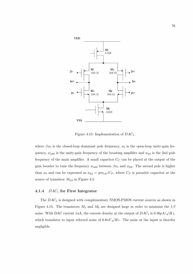
76
Figure 4.15: Implementation of DAC1.
where βwt is the closed-loop dominant pole frequency, wt is the open-loop unity-gain fre-
quency, wadd is the unity-gain frequency of the boosting amplifier and wp2 is the 2nd pole
frequency of the main amplifier. A small capacitor CC can be placed at the output of the
gain booster to tune the frequency wadd between βwt and wp2. The second pole is higher
than wt and can be expressed as wp2 = gm5,6/CP , where CP is parasitic capacitor at the
source of transistor M5,6 in Figure 4.5.
4.1.4 DAC1 for First Integrator
The DAC1 is designed with complementary NMOS-PMOS current sources as shown in
Figure 4.15. The transistors M5 and M6 are designed large in order to minimize the 1/f
noise. With DAC current 1uA, the current density at the output of DAC1 is 0.56pA/√Hz,
which translates to input referred noise of 0.8nV√Hz. The noise at the input is therefor
negligible.

77
Figure 4.16: Feedback integrator.
4.2 Feedback Integrator
The feedback integrator of overall system is in Figure 4.16. The circuit implementation
of op-amp, GM stage, and DAC2 are discussed in this section.
4.2.1 Op-Amp for Second Integrator
In order to enable wide ICMR for pre-amplifier, a two-stage amplifier is used based on
its wide output swings property as shown in Figure 4.17 . Since the speed of feedback path
is relative low, the low power design can be achieved by using small current.
The gain of first and second stages are gm1,2/gm3,4 and B × gm3,4 × rO5,O6||rO7,O8
respectively. Thus, the total gain of amplifier is
AV =gm1,2
gm3,4×B × gm3,4 × rO5,O6||rO7,O8
= B × gm1,2 × rO5,O6||rO7,O8. (4.28)
where B is the factor of drain current Id1,d2. The gain of the amplifier can be made large
by increasing the factor B. The operating points for each device are summarized in Table
4.2

78
Figure 4.17: Op-amp for feedback integrator.
Table 4.2: Operating point for each transistor of op-amp.
Devices ID(uA) VGS-Vth (mV) gm (uA/V)
M1,M2 6.5 4 171
M3, M4 6.5 282 41
M5, M6 6.5 282 41
M7, M8 6.5 190 61
Noise Analysis
In section 3.4.3, the total input referred noise is shown in equation (3.54). The input
referred noise is analyzed first in order to find the noise at output. The noise of M5 and
M7 referred to the gate of M5 is equal to 4kT (2/3)(B × gm3 + gm7)/(B × gm3)2, which
is divided by gm1/gm32 when referred to the main input. Transistors M1 and M3 produce
an input-referred noise of (8kT/3)(gm3 + gm1)/gm21. Thus, the total input-referred noise
equals

79
V 2in,n =
8
3kT (
B × gm3 + gm7
B × gm3
2
) +8
3kT
1
gm21
(gm1 + gm3)
=8
3kT
1
gm21
[gm3
B+
gm7
B2+ gm1 + gm3]. (4.29)
If gm1 is larger than gm3 and B is greater than one, the input referred noise is determined
by the first stage and can be approximated by
V 2in,n
∼=8
3kT
1
gm1. (4.30)
Based on Figure 4.16, the noise at the output is limited by the off-chip capacitor CL
and is expressed as
V 2out,n =
8
3kT
1
gm1
1
β2
gm1
CL2π
π
2
=1
β2
2kT
3CL. (4.31)
where β = (CF +CP )/CF . Thus, the noise at the output is limited by the capacitor CL and
has no effect on gm1. Since the capacitor CL is off-chip and can be made very large, the
total input referred noise is then dominated by the input noise of pre-amplifier according
to equation (3.54). Also, the devices of op-amp are made large, 1/f noise is negligible based
on (2.10).
4.2.2 GM stage circuit for feedback integrator
The CMFB of feedback op-amp is the GM stage to enable wide ICMR for the pre-
amplifier as shown in Figure 3.1. The GM stage has not only no noise effect at the input
but also no extra power consumption for the overall system. The GM stage is designed
based on the concept of CMFB in section 4.1.3. The source degeneration is applied in order
to improve linearity for wide ICMR. The implementation of GM stage is shown in Figure
4.18.

80
Figure 4.18: CMFB as GM stage for Overall System.
Figure 4.19: Transconductance vs. ICMR.
The simulation result for GM stage is shown in Figure 4.19. The transconductance of
pre-amplifier is linear between ±0.3V ICMR. The common mode signal or noise will be
subtracted by the pre-amplifier at the input.

81
Figure 4.20: State Machine for UP-DOWN Counter.
4.2.3 UP-DOWN Counter
Figure 4.20 shows the state machine for the behavior of UP-DOWN digital counter. The
description of behavior is as follow: When the reset is high, R is equal to 2N/2. During
state S1, a digital output of quantizer D is detected, if the D is logic low, state S1 goes to
state S2, and R is subtracted by one, and vice versa. In state S2 or S3, if R is equal to 0 or
2N , its value is reset and goes back to state S1 while producing an output signal En logic
high or low depending on the R is equal to 2N or 0. With digital feedback from Σ∆ output,
quantization noise in high frequency domain also goes through the UP-DOWN counter.
Therefore, the UP-DOWN counter must be designed with low-pass filter characteristic in
order to reject quantization noise in high frequency domain. With ideal Σ∆ ADC operation,
if the input is higher than the reference voltage, more high logics will present at the output.
In the other hand, more low logics will present at the output when the input is lower than
the reference voltage. A signal or noise at high frequency will present logic high or logic low
in a short period of time at the digital output. Therefore, increasing the number of bit of
UP-DOWN counter will make the output of the counter never go high or low according to
the operation of Σ∆ ADC in time domain. Thus, the feedback integrator is not activated
by the UP-DOWN counter, the behavior of UP-DOWN counter is analogous to LPF.

82
Figure 4.21: Implementation of Feedback DAC2.
4.2.4 DAC2 for Feedback Integrator
The circuit implementation of feedback DAC2 is shown in Figure 4.21. The UPa and
DWa signals are the outputs of UP-DOWN digital counter, and the UP and DW signals are
delay signals of UPa and DWa in order to make charge-injection signal independent. The
step size is the ratio between CF and CS , and low-frequency cutoff is determined by (3.62).
The outputs VfbP and VfbM are then fed back to input of pre-amplifier.
4.3 Quantizer
The circuit implementation of quantizer is shown in Figure 4.22. This component con-
tains of a regenerative latch and two D flip flops (DFF). The latch has two back to back
inverters whose outputs are tied together with PMOS transistors. When the PMOS tran-
sistors M7 and M8 are on, the outputs of the inverters are held together and the latch is
in tracking mode. After a short of period, both currents of inverters are equal by turning
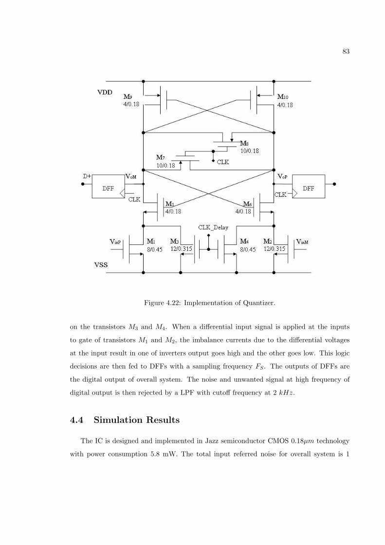
83
Figure 4.22: Implementation of Quantizer.
on the transistors M3 and M4. When a differential input signal is applied at the inputs
to gate of transistors M1 and M2, the imbalance currents due to the differential voltages
at the input result in one of inverters output goes high and the other goes low. This logic
decisions are then fed to DFFs with a sampling frequency FS . The outputs of DFFs are
the digital output of overall system. The noise and unwanted signal at high frequency of
digital output is then rejected by a LPF with cutoff frequency at 2 kHz.
4.4 Simulation Results
The IC is designed and implemented in Jazz semiconductor CMOS 0.18µm technology
with power consumption 5.8 mW. The total input referred noise for overall system is 1

84
Table 4.3: Input Noise Summary for EEG, ECG, and EMG.
ECG EEG EMG Total Input Referred Noise
Frequency (Hz) 0.05-100 0.1-100 20-2000 0-2000
Noise (uVrms) 0.54 0.51 0.72 1
uV rms as shown in Figure 4.23. The input referred noise for EEG, ECG, and EMG are
also summarized in Table 4.3.
The CMRR is 102 dB as shown at the top of Figure 4.24. An input signal with amplitude
Figure 4.23: Total input referred noise.
101
102
103
104
105
106
20
40
60
80
100
120
Frequency
dB
Common mode rejection ratio
101
102
103
104
105
106
10−15
10−10
10−5
100
PSD plot
Frequency
V2
Observed PSDPredicted PSD
SNR = 61 dB
Figure 4.24: CMRR on the top and predicted and observed PSD on the bottom.
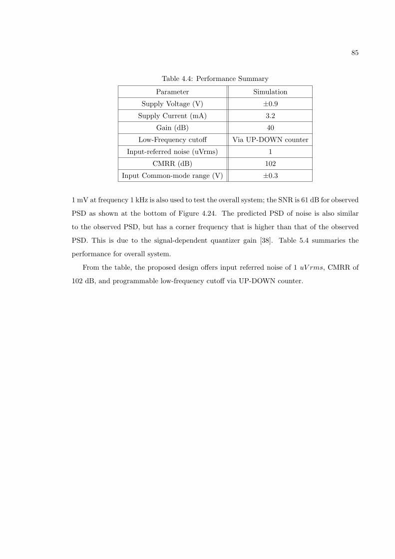
85
Table 4.4: Performance Summary
Parameter Simulation
Supply Voltage (V) ±0.9
Supply Current (mA) 3.2
Gain (dB) 40
Low-Frequency cutoff Via UP-DOWN counter
Input-referred noise (uVrms) 1
CMRR (dB) 102
Input Common-mode range (V) ±0.3
1 mV at frequency 1 kHz is also used to test the overall system; the SNR is 61 dB for observed
PSD as shown at the bottom of Figure 4.24. The predicted PSD of noise is also similar
to the observed PSD, but has a corner frequency that is higher than that of the observed
PSD. This is due to the signal-dependent quantizer gain [38]. Table 5.4 summaries the
performance for overall system.
From the table, the proposed design offers input referred noise of 1 uV rms, CMRR of
102 dB, and programmable low-frequency cutoff via UP-DOWN counter.

86
Chapter 5
Test Chip Results
5.1 Signal Reconstruction
The off-chip LPF is used to reject the quantization noise at high frequencies as shown
in Figure 3.1. It also acts as anti-aliasing filter to limit the bandwidth of signal of interest.
The signal reconstruction can be done by the process of averaging filter function and a rate
reduction function. This process is also known as decimation [57].
Since the output signal of system is a single-bit data stream, a high-order linear-phase
finite-impulse-response (FIR) LPF is used. The output of FIR LPF can be expressed
Y (k) = a0X(k) + a1X(k − 1) + . . .+ anX(k − n). (5.1)
where X(k) is the input sequence, n is the order, and ai the filter coefficients. The advantage
of FIR LPF is nonrecursive property based on (5.1). Although FIR filter takes more time
to perform the decimation filtering process than infinite-impulse-response (IIR) filter for
the same passband and out-of-band frequency characteristics, FIR filter can be designed to
have a linear-phase response which is required for instrumentation applications. A 10000
order FIR LPF is designed with cutoff frequency at 2 kHz as shown in Figure 5.1. The
phase response is linear over frequency 0-2 kHz. An input signal with amplitude 1mV at 1
kHz is used to test the system, the digital outputs are compared at the top of Figure 5.2.
The input signal is reconstructed and shown at the bottom of Figure 5.2.
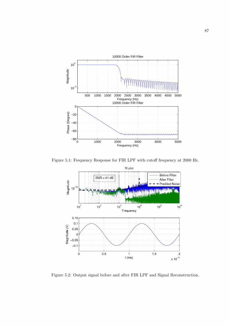
87
500 1000 1500 2000 2500 3000 3500 4000 4500 5000
10−5
100
10000 Order FIR Filter
Frequency (Hz)
Mag
nitu
de
0 1000 2000 3000 4000 5000−80
−60
−40
−20
010000 Order FIR Filter
Frequency (Hz)
Pha
se (
Deg
ree)
Figure 5.1: Frequency Response for FIR LPF with cutoff frequency at 2000 Hz.
Figure 5.2: Output signal before and after FIR LPF and Signal Reconstruction.

88
Figure 5.3: Die photo for Biomedical IC
5.2 Chip Evaluation
The overall system is fabricated on a chip with total area 0.25 mm2. The photo die of
circuitry is shown in Figure 5.3. The power supplies, reference voltages, timing signals ,
and input attenuator are required in order to test the biomedical IC. The implementation
of circuits are discussed in this section.
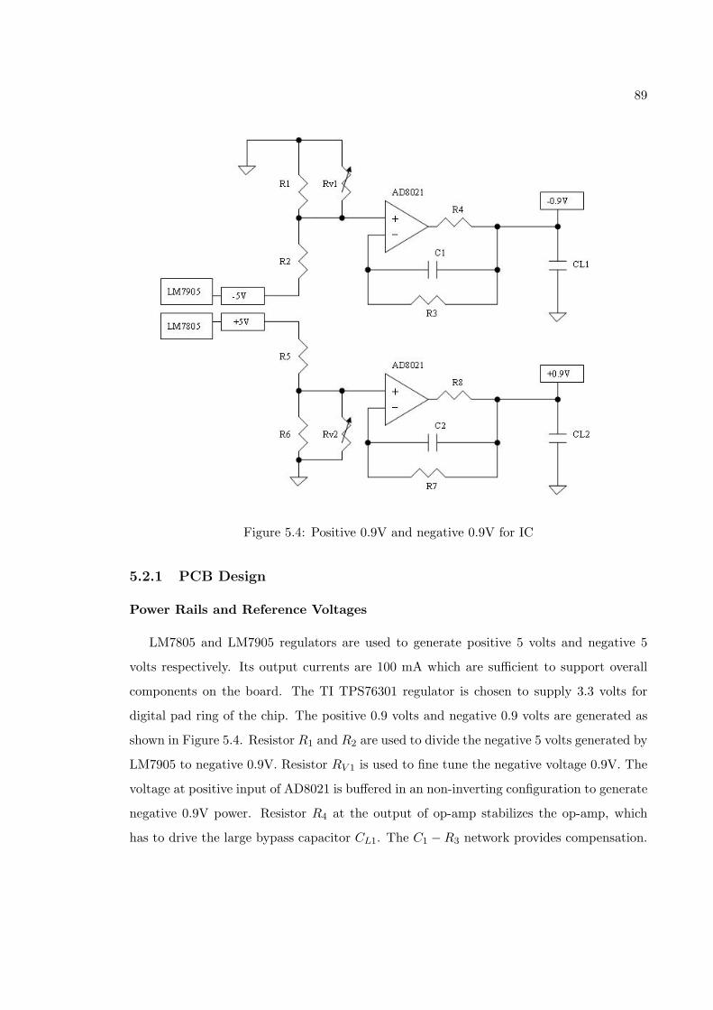
89
Figure 5.4: Positive 0.9V and negative 0.9V for IC
5.2.1 PCB Design
Power Rails and Reference Voltages
LM7805 and LM7905 regulators are used to generate positive 5 volts and negative 5
volts respectively. Its output currents are 100 mA which are sufficient to support overall
components on the board. The TI TPS76301 regulator is chosen to supply 3.3 volts for
digital pad ring of the chip. The positive 0.9 volts and negative 0.9 volts are generated as
shown in Figure 5.4. Resistor R1 and R2 are used to divide the negative 5 volts generated by
LM7905 to negative 0.9V. Resistor RV 1 is used to fine tune the negative voltage 0.9V. The
voltage at positive input of AD8021 is buffered in an non-inverting configuration to generate
negative 0.9V power. Resistor R4 at the output of op-amp stabilizes the op-amp, which
has to drive the large bypass capacitor CL1. The C1 −R3 network provides compensation.

90
Table 5.1: Components for 0.9V and -09V.
Components -0.9V Components +0.9V
R1 200 ohm R5 820 ohm
R2 820 ohm R6 200 ohm
R3 1 kohm R7 1 kohm
R4 1 ohm R8 1 ohm
C1 0.1 uF C5 0.1 uF
CL1 1 uF CL2 1 uF
Figure 5.5: Input Attenuator
The same idea is applied to generate the positive 0.9V power, -Vref, and +Vref for DAC2.
Table 5.1 summaries the components for 0.9V and -0.9V.
Input Attenuator
In order to test the IC, an input signal with 1mV amplitude and low noise is required.
An input attenuator is deigned with low noise as shown in Figure 5.5. Resistors R1 and
R2 are voltage attenuator to divide 1 V input signal from function generator to 1 mV.
Capacitor C is used to limit the bandwidth while keeping the noise of kT/2C.
Timing Signals
The sampling frequency FS and chopping signals FC are generated from crystal oscil-
lator. The Spartan-3 Starter board is used with VHDL code to generate the sampling
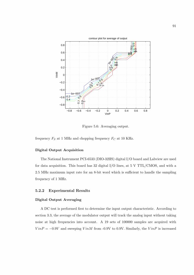
91
1e−0
07
1e−0
07
1e−007
1e−007
0.2
0.2
0.2
0.2
0.4
0.4
0.4
0.4
0.5
0.5
0.5
0.5
0.7
0.7
0.7
0.7
0.9
0.9
0.9
0.9
1
1
1
1
contour plot for average of output
VinP
Vin
M
−0.8 −0.6 −0.4 −0.2 0 0.2 0.4 0.6 0.8
−0.8
−0.6
−0.4
−0.2
0
0.2
0.4
0.6
0.8
Figure 5.6: Averaging output.
frequency FS at 1 MHz and chopping frequency FC at 10 KHz.
Digital Output Acquisition
The National Instrument PCI-6533 (DIO-32HS) digital I/O board and Labview are used
for data acquisition. This board has 32 digital I/O lines, at 5 V TTL/CMOS, and with a
2.5 MHz maximum input rate for an 8-bit word which is sufficient to handle the sampling
frequency of 1 MHz.
5.2.2 Experimental Results
Digital Output Averaging
A DC test is performed first to determine the input output characteristic. According to
section 3.3, the average of the modulator output will track the analog input without taking
noise at high frequencies into account. A 19 sets of 100000 samples are acquired with
V inP = −0.9V and sweeping V inM from -0.9V to 0.9V. Similarly, the V inP is increased
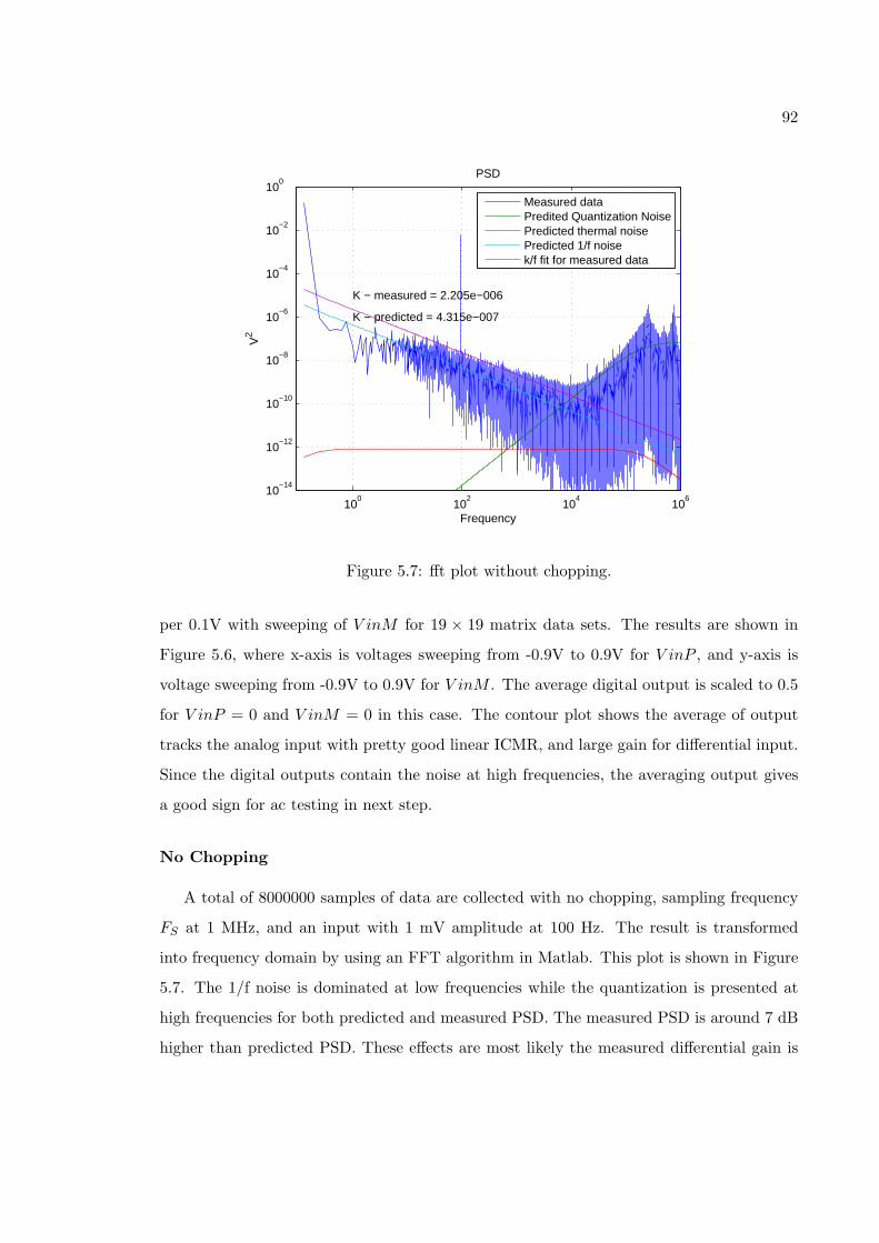
92
100
102
104
106
10−14
10−12
10−10
10−8
10−6
10−4
10−2
100
Frequency
V2
PSD
K − measured = 2.205e−006
K − predicted = 4.315e−007
Measured dataPredited Quantization NoisePredicted thermal noisePredicted 1/f noisek/f fit for measured data
Figure 5.7: fft plot without chopping.
per 0.1V with sweeping of V inM for 19 × 19 matrix data sets. The results are shown in
Figure 5.6, where x-axis is voltages sweeping from -0.9V to 0.9V for V inP , and y-axis is
voltage sweeping from -0.9V to 0.9V for V inM . The average digital output is scaled to 0.5
for V inP = 0 and V inM = 0 in this case. The contour plot shows the average of output
tracks the analog input with pretty good linear ICMR, and large gain for differential input.
Since the digital outputs contain the noise at high frequencies, the averaging output gives
a good sign for ac testing in next step.
No Chopping
A total of 8000000 samples of data are collected with no chopping, sampling frequency
FS at 1 MHz, and an input with 1 mV amplitude at 100 Hz. The result is transformed
into frequency domain by using an FFT algorithm in Matlab. This plot is shown in Figure
5.7. The 1/f noise is dominated at low frequencies while the quantization is presented at
high frequencies for both predicted and measured PSD. The measured PSD is around 7 dB
higher than predicted PSD. These effects are most likely the measured differential gain is

93
100
102
104
106
10−14
10−12
10−10
10−8
10−6
10−4
10−2
100
Frequency
V2
PSD
K − measured = 8.897e−008
K − predicted = 4.315e−010
Measured dataPredited Quantization NoisePredicted thermal noise and 1/f noisek/f fit for measured data
Figure 5.8: fft plot with chopping with input 1 mV amplitude at 100 Hz .
higher than the predicted one. In addition, the K constants for 1/f noise are 2.2e− 6V 2 · f
and 4.3e − 7V 2 · f for measured and predicted data respectively. The measured data of
K constant is 5 times larger than the predicted data from Cadence simulation. The PSD
between measured and predicted data are acceptable for no chopping test. Notice that,
SNR is determined by 1/f noise since the chopping blocks are not enable in this case.
With Chopping
A total of 8000000 samples of data are again acquired with sampling frequency FS at
1 MHz, chopping frequency FC at 10 KHz, and an input with 1 mV amplitude at 100
HZ. The PSD for predicted and measured data are shown in Figure 5.8. The 1/f noise of
pre-amplifier is modulated and translated to the odd harmonic chopping frequencies in this
case. However, the even harmonic chopping signals are still presented at high frequencies
due to the duty cycle of chopping signals are not exactly 50 percent. There is another
1/f noise source due to first integrator amplifier at low frequencies as shown in Figure 5.8.
The corner frequency between 1/f noise and thermal noise are less than 100 Hz and over

94
Table 5.2: Signal and Noise powers summary.
CASE A B C D E
[ϕ1,ϕ2] [1,0] [0,1] [FC ,0] [0,FC ] [FC ,FC ] unit
Signal Power 0.0049 0.0059 0.0012 0.0014 0.0054 v2
Noise Power 2.37e-5 2.6e-5 9.82e-6 1.08e-5 8.45e-6 v2
SNR 23.1 23.58 20.9 21.33 28.07 dB
1 KHz for predicted PSD and measured PSD respectively. The K constants of 1/f noise
for predicted and measured data are 4.3e − 10v2 · f and 8.9e − 8v2 · f , resulting in 23 dB
difference. With integral PSD over frequency 0.25-2 kHz, the SNR is 28dB which is lower
than the one we predicted in Chapter 3.
Table 5.2 summaries the signal and noise powers for different cases. The SNR is 23 dB
without chopping for cases A and B. For cases C and D, one of chopping signals connects
to FC at 10 KHz and the other connects to negative rail, the signal power is reduce to 1/4
compare with cases A and B. When the chopping is applied for case E, the signal power is
0.0054V 2 which is almost equal to no chopping cases A and B. The SNR is improved 5dB
with chopping technique based on Table 5.2.
−4.5 −4 −3.5 −3 −2.5 −20
10
20
30
40
50
60
70
80
Input Level log(V)
SN
R,S
ND
R (
dB)
Ideal SNRSNR for 50HzSNDR for 50HzSNR for 1kHZSNDR for 1kHz
Figure 5.9: SNR and SNDR vs. Input Amplitude.

95
Figure 5.10: Problems for 1/f noise.
Figure 5.9 shows the relationship between input amplitude and SNR. The black line
represents the ideal case while the red and blue lines are input signals at 50 Hz and 1 kHz
respectively. From the Figure, the observed SNR is 20 dB lower than the predicted one
due to the 1/f noise of first integrator amplifier. Also, the SNR is proportional to input
amplitude and reaches peak value at amplitude of 100 mV. This is caused by the decrease
of the gain of quantizer as the amplitude is increased. The decrease in gain of quantizer
changes the shape of noise transfer function, causing the noise to move inside the band of
interest [38,58]. For SNDR, it reaches the peak value at amplitude 1mV and decreases with
increasing amplitude. This is due to the non-linear effects of pre-amplifier and quantizer.
Figure 5.9 also shows the SNR and SNDR is frequency independent.
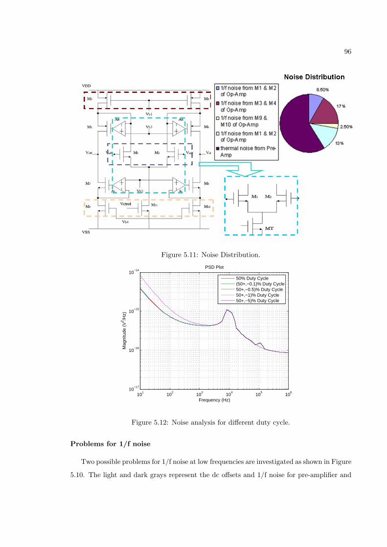
96
Figure 5.11: Noise Distribution.
101
102
103
104
105
106
10−17
10−16
10−15
10−14
PSD Plot
Frequency (Hz)
Mag
nitu
de (
V2 /H
z)
50% Duty Cycle(50+,−0.1)% Duty Cycle50+,−0.5)% Duty Cycle50+,−1)% Duty Cycle50+,−5)% Duty Cycle
Figure 5.12: Noise analysis for different duty cycle.
Problems for 1/f noise
Two possible problems for 1/f noise at low frequencies are investigated as shown in Figure
5.10. The light and dark grays represent the dc offsets and 1/f noise for pre-amplifier and
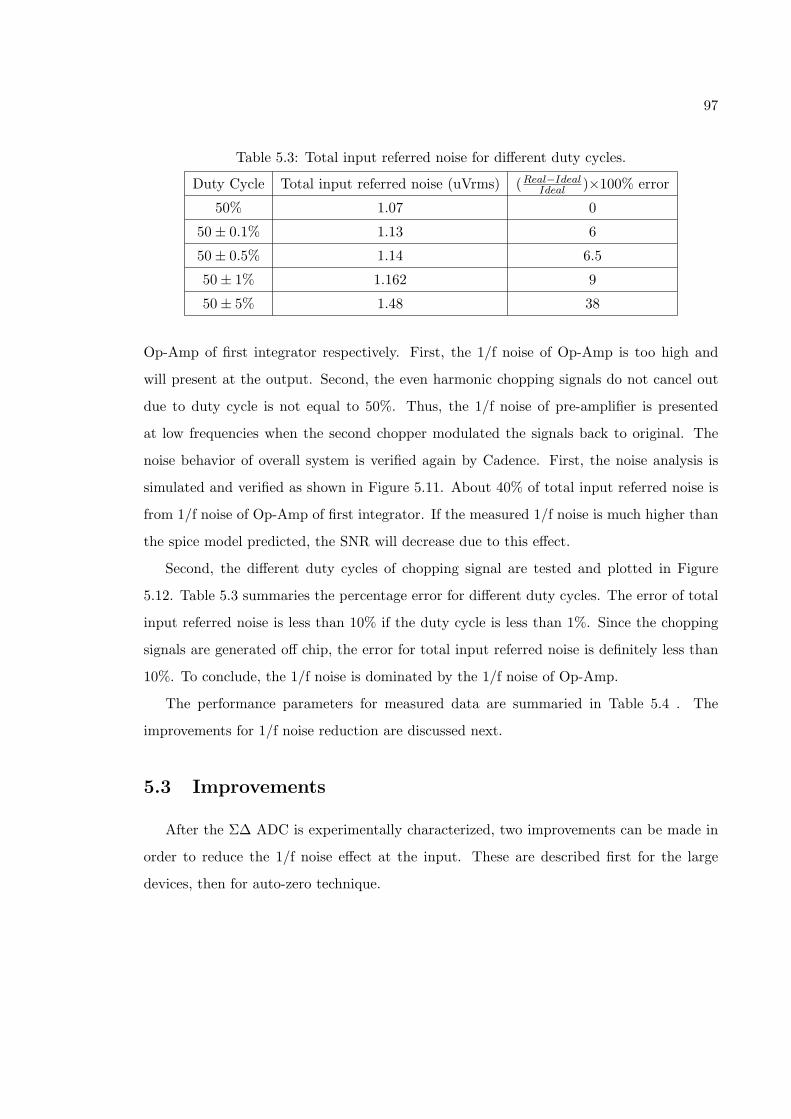
97
Table 5.3: Total input referred noise for different duty cycles.
Duty Cycle Total input referred noise (uVrms) (Real−IdealIdeal )×100% error
50% 1.07 0
50± 0.1% 1.13 6
50± 0.5% 1.14 6.5
50± 1% 1.162 9
50± 5% 1.48 38
Op-Amp of first integrator respectively. First, the 1/f noise of Op-Amp is too high and
will present at the output. Second, the even harmonic chopping signals do not cancel out
due to duty cycle is not equal to 50%. Thus, the 1/f noise of pre-amplifier is presented
at low frequencies when the second chopper modulated the signals back to original. The
noise behavior of overall system is verified again by Cadence. First, the noise analysis is
simulated and verified as shown in Figure 5.11. About 40% of total input referred noise is
from 1/f noise of Op-Amp of first integrator. If the measured 1/f noise is much higher than
the spice model predicted, the SNR will decrease due to this effect.
Second, the different duty cycles of chopping signal are tested and plotted in Figure
5.12. Table 5.3 summaries the percentage error for different duty cycles. The error of total
input referred noise is less than 10% if the duty cycle is less than 1%. Since the chopping
signals are generated off chip, the error for total input referred noise is definitely less than
10%. To conclude, the 1/f noise is dominated by the 1/f noise of Op-Amp.
The performance parameters for measured data are summaried in Table 5.4 . The
improvements for 1/f noise reduction are discussed next.
5.3 Improvements
After the Σ∆ ADC is experimentally characterized, two improvements can be made in
order to reduce the 1/f noise effect at the input. These are described first for the large
devices, then for auto-zero technique.
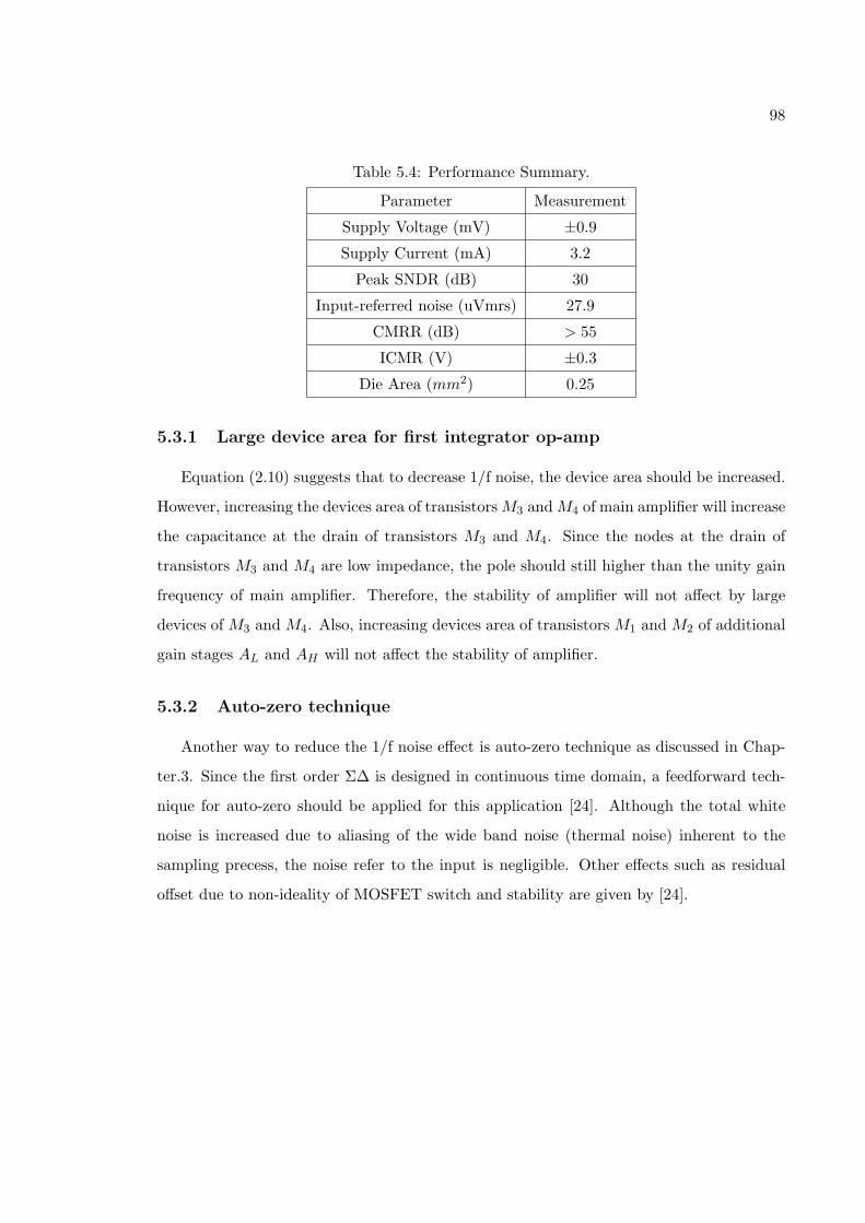
98
Table 5.4: Performance Summary.
Parameter Measurement
Supply Voltage (mV) ±0.9
Supply Current (mA) 3.2
Peak SNDR (dB) 30
Input-referred noise (uVmrs) 27.9
CMRR (dB) > 55
ICMR (V) ±0.3
Die Area (mm2) 0.25
5.3.1 Large device area for first integrator op-amp
Equation (2.10) suggests that to decrease 1/f noise, the device area should be increased.
However, increasing the devices area of transistorsM3 andM4 of main amplifier will increase
the capacitance at the drain of transistors M3 and M4. Since the nodes at the drain of
transistors M3 and M4 are low impedance, the pole should still higher than the unity gain
frequency of main amplifier. Therefore, the stability of amplifier will not affect by large
devices of M3 and M4. Also, increasing devices area of transistors M1 and M2 of additional
gain stages AL and AH will not affect the stability of amplifier.
5.3.2 Auto-zero technique
Another way to reduce the 1/f noise effect is auto-zero technique as discussed in Chap-
ter.3. Since the first order Σ∆ is designed in continuous time domain, a feedforward tech-
nique for auto-zero should be applied for this application [24]. Although the total white
noise is increased due to aliasing of the wide band noise (thermal noise) inherent to the
sampling precess, the noise refer to the input is negligible. Other effects such as residual
offset due to non-ideality of MOSFET switch and stability are given by [24].

99
Chapter 6
Conclusion and Future Work
6.1 Conclusion
A bio-potential acquisition system is presented in this thesis. The background of bio-
potential signals and existing work are introduced in Chapter 1. The specifications and
analog requirements for extracting bio-potential signals are discussed in Chapter 2. A novel
second order Σ∆ ADC with feedback integrator to program the low frequency cutoff is
introduced in Chapter 3. In order to improve wide ICMR, the CMFB circuit of feedback
integrator is used as GM stage to provide wide ICMR to subtract the CM signals at the
input by the pre-amplifier. The noise issues and bandwidth selection also are analyzed.
In Chapter 4, the circuit implementation of each block is designed and discussed. The
simulation results of overall system are met the specifications with input referred noise 1
uVmrs, the control of low frequency cutoff via N-bit counter, CMRR of 102 dB, and ICMR
± 0.3V.
In Chapter 5, the system is fabricated in 0.18 um CMOS technology with total die area
0.25mm2. The measured SNR is around 20 dB lower then the predicted one. The 1/f noise
of pre-amplifier is translated to high frequencies by the chopping technique. However, the
1/f noise of Op-Amp of first integrator is amplified and presented at the outputs. This
effect results in decreasing the SNR for the system.
100
6.2 Future Work
Two ways to improve the 1/f noise are discussed in 5.3. First, the large size of transistors
can be made to reduce the 1/f noise effect. Since the parasitic capacitance is proportional
to the total area of transistor, the second pole at the low impedance node will move to lower
frequency. The stability problem should be considered if the second pole is less than three
times of dominant pole.
Second, if the auto-zero technique is used in the future. It is best to apply for both
Pre-Amplifier and Op-Amp of first integrator. Although the white noise will increase as
discussed in Chapter. 3, it provides very large input impedance to buffer the input voltages
from the electrodes. With improvement of circuitry in the future, the IC presented in this
thesis can be used as one of multi-channel bio-medical applications.
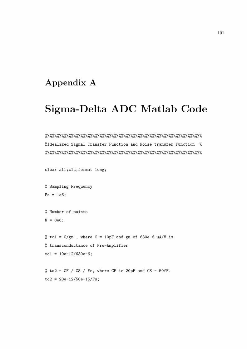
101
Appendix A
Sigma-Delta ADC Matlab Code
%%%%%%%%%%%%%%%%%%%%%%%%%%%%%%%%%%%%%%%%%%%%%%%%%%%%%%%%%%%%%%%%%%
%Idealized Signal Transfer Function and Noise transfer Function %
%%%%%%%%%%%%%%%%%%%%%%%%%%%%%%%%%%%%%%%%%%%%%%%%%%%%%%%%%%%%%%%%%%
clear all;clc;format long;
% Sampling Frequency
Fs = 1e6;
% Number of points
N = 8e6;
% to1 = C/gm , where C = 10pF and gm of 630e-6 uA/V is
% transconductance of Pre-Amplifier
to1 = 10e-12/630e-6;
% to2 = CF / CS / Fs, where CF is 20pF and CS = 50fF.
to2 = 20e-12/50e-15/Fs;
102
% b is gain of STF and set by the ratio of DAC1 and DAC2
b= .01;
f = Fs/N:Fs/N:Fs;
s = i*f*2*pi;
% Nb is number of bit for UP-DW counter.
Nb = 18;
% Signal Transfer Function (STF)
num = [0 to2 0];
den = [to1*to2 b*to2 2^(-Nb)];
h = polyval(num,s)./polyval(den,s);
% Noise Transfer Function (NTF)
numn = [to1*to2 0 0];
denn = [to1*to2 b*to2 2^(-Nb)];
hn = polyval(numn,s)./polyval(denn,s);
% Compare STF and NTF
% figure(1)
% loglog(f,abs(h),f,abs(hn));grid;
% xlabel(’Frequency’);ylabel(’Magnitude’);title(’NTF & STF’);
% axis tight
%%%%%%%%%%%%%%%%%%%%%%%%%%%%%%%%%%%%%%%%%%%%%%%%%%%%%%%%%%%%%%%%%%
% Models for 1/f, white, and quantization Noise %
%%%%%%%%%%%%%%%%%%%%%%%%%%%%%%%%%%%%%%%%%%%%%%%%%%%%%%%%%%%%%%%%%%

103
%%%%%%%%%%%%%%%%%%%%%%
% Quantization noise %
%%%%%%%%%%%%%%%%%%%%%%
% step size for 1-bit quantizer is 1.8V.
VLsb = 1.8/sqrt(12);
% Quantization noise at the input
Vq = VLsb*ones(1,N)/sqrt(Fs);
% Quantization noise at the output.
VVq = (Vq.*abs(hn)).^2;
%%%%%%%%%%%%%%%%%%%%%%
% White noise %
%%%%%%%%%%%%%%%%%%%%%%
% the total thermal noise is 9nV/sqrt(Hz) based on cadence simulation
whitenoise = 9e-9;
% thermal or white noise at the input
Vw = whitenoise*ones(1,N);
% white noise at the output
VVw = (Vw.*abs(h)).^2;
%%%%%%%%%%%%%%%%%%%%%%
% 1/f noise %
%%%%%%%%%%%%%%%%%%%%%%

104
% K constants for 1/f noise, the Ks are found by cadence simulation
% where K_cadeno and K_cadeni are K fit for output and input respectively
K_cadeno = 4.315451793498000e-007
K_cadeni = 1.368851885114884e-004;
% 1/f noise at the input
Vf = K_cadeni ./ f;
% 1/f noise at the output
VVf = K_cadeno ./ f;
%%%%%%%%%%%%%%%%%%%%%%%%%%%%%%%%%%%%%%%%%%%%%%%%%%%%%%%%%%
%%% find fk %
%%% %
% f_k = f(1:1001); %
% k_caden = f_k.*maout(1:1001); %
% K_caden = mean(k_caden); %
% flick_fit = K_caden./f; %
%%% %
%%% %
%%%%%%%%%%%%%%%%%%%%%%%%%%%%%%%%%%%%%%%%%%%%%%%%%%%%%%%%%%
% Chopping model for n = 1, 3 ,5 harmonics only.
% where Fchop = 10 KHz.
Fchop1 = 10e3;

105
Fchop3 = 30e3;
Fchop5 = 50e3;
FC1 = round(Fchop1*N/Fs);
FC3 = round(Fchop3*N/Fs);
FC5 = round(Fchop5*N/Fs);
maoutn = (Vf./b).^2 + (Vw./b).^2;
maout_rot = rot90(maoutn,2);
maout_t = [maout_rot(1:end-1) maoutn];
right1 = [zeros(1,FC1) maout_t(1:length(maout_t)-FC1)];
left1 = [maout_t(FC1+1:end) zeros(1,FC1)];
right3 = [zeros(1,FC3) maout_t(1:length(maout_t)-FC3)];
left3 = [maout_t(FC3+1:end) zeros(1,FC3)];
right5 = [zeros(1,FC5) maout_t(1:length(maout_t)-FC5)];
left5 = [maout_t(FC5+1:end) zeros(1,FC5)];
maout_T = (pi/2)^2*(right1 + left1 + 1/3^3*(right3 + left3)
+ 1/5^5*(right5 + left5));
maout_Tp = maout_T(N:length(maout_T));
% 1/f noise at the output
maout_Tm = maout_Tp.*abs(h)*b;
% Comparison for no chopping and with Chopping
% figure(2)
% loglog(f,VVf.*abs(h).*b,f,maout_Tm);grid
% xlabel(’Frequency’);ylabel(’V^2’);title(’compare 1/f’)
% legend(’no chopping’,’with chopping’)
%%%%%%%%%%%%%%%%%%%%%%%%%%%%%%%%%%%%%%%%%%%%%%%%
% Total plot for Vn(1/f), Vn(white), Vq noise %
%%%%%%%%%%%%%%%%%%%%%%%%%%%%%%%%%%%%%%%%%%%%%%%%

106
% figure(3)
% loglog(f,Vq,f,Vw,f,Vf);grid
% xlabel(’Frequency’);ylabel(’V/sqrt(Hz)’);title(’PSD for
Quantization, white and 1/f Noise at input’)
% legend(’Quantization Noise’,’White noise’,’1/f noise’);
% figure(4)
% loglog(f,VVq,f,maout_Tm + VVw);grid
% axis([10^1 10^6 10^-12 10^-1])
% xlabel(’Frequency’);ylabel(’V^2’);title(’PSD for Quantization,
white and 1/f Noise at output’)
% legend(’Quantization Noise’,’1/f and White noise with chop’);
%%%%%%%%%%%%%%%%%%%%%%%%%%%%%%%%%%%%%%
% 1mvp-p signal @ 100Hz test %
%%%%%%%%%%%%%%%%%%%%%%%%%%%%%%%%%%%%%%
% fin = 100;
% t= 0:1/Fs:100e-3;
% x = .5e-3*sin(2*pi*fin*t);
% xf = abs(fft(x))/length(t);
% xff = (xf.*abs(h)).^2;
%%%%%%%%%%%%%%%%%%%%%%%%%%%%%%%%%%%%%%%%%%%%%%%%%%%%%%%%%%%%%
% Total plot for Vin @ 100Hz Vn(1/f), Vn(white), Wq noise %
%%%%%%%%%%%%%%%%%%%%%%%%%%%%%%%%%%%%%%%%%%%%%%%%%%%%%%%%%%%%%
% figure(5)
% loglog(f,VVq,f,VV_fw,f,xff);grid

107
% axis([10^1 10^6 10^-12 10^-1])
% xlabel(’Frequency’);ylabel(’V^2’);title(’PSD for Quantization,
white and 1/f Noise at output’)
% legend(’Quantization Noise’,’1/f and White noise’,’input test signal’);
%%%%%%%%%%%%%%%%%%%%%%%%%%%%%%%%%%%%%%
% Measured data %
%%%%%%%%%%%%%%%%%%%%%%%%%%%%%%%%%%%%%%
% Read measured data
B = csvread(’input.csv’,1);
Nd = length(B);
fd = Fs/Nd:Fs/Nd:Fs;
D1 = fft(B)/Nd;
PP = D1.*conj(D1);
% PSD plot for measured data
% figure(6)
% loglog(fd,PP)
% xlabel(’Frequency’);ylabel(’V^2’);title(’PSD’);grid
% axis([10^1 10^6 10^-12 10^-1])
% PSD plots for measured data, quantization noise, 1/f noise,
% and white noise at output
% figure(7)
% loglog(fd,PP,f,VVq,f,maout_Tm,f,VVw);grid
% xlabel(’Frequency’);ylabel(’V^2’);title(’PSD’)
% legend(’Measured data’,’Quantization Noise’,’1/f and White noise’);
% axis([10^1 10^6 10^-12 10^-1])

108
% PSD plots for measured data and total noise at output
% figure(8)
totalnoise = VVq + maout_Tm + VVw;
% loglog(fd,PP,f,totalnoise);grid
% hold on
% xlabel(’Frequency’);ylabel(’V^2’);title(’PSD’)
% axis([1e-1 10^6 10^-12 10^-1])
% SNR for predicted and measured data
% where vinf is input signal at 96 Hz from function generator.
vinf = 96;
sig = round(Nd / Fs * vinf);
% Select the signal for plus and minus 20 bins
S_bin = sig + [-20:20];
% Select the bandwidth from 0.25 Hz to 2 kHz
FL = .25; FH = 2000;
in_band = round(FL*Nd/Fs:Nd/Fs*FH);
noise_bin = setdiff(in_band,S_bin);
% Noise power for measured data
NP_m = sum(PP(int32(noise_bin)))
% signal power for measured data
Sig_P = sum(PP(int32(S_bin)))
% SNR for measured date
SNR = 10*log10(Sig_P/NP_m)

109
% noise power for predicted data
NP_p = sum(totalnoise(int32(in_band)))
% s = sprintf( ’Noise Power - measured = %0.4g’,NP_m);
% s1 = sprintf( ’Noise Power - predicted = %0.4g’,NP_p);
% text(1.2e2,1e-6,s)
% text(1.2e2,1e-8,s1)
%%%%%%%%%%%%%%%%%%%%%%%%%%%%%%%%%%%%%%%%%%%%%%%%%%%%%%%%%%%%%%%%%%%%
% Comparison of K constants for predicted and measured data
%%%%%%%%%%%%%%%%%%%%%%%%%%%%%%%%%%%%%%%%%%%%%%%%%%%%%%%%%%%%%%%%%%%%%
% K fit from 1 Hz to 90 Hz for measured data
fl = 1;fh = 90;
f_in = round(fl*Nd/Fs:fh*Nd/Fs);
f_k = f(f_in);
% k for measured data
k_measu = f_k.*PP(f_in)’;
K_measu = mean(k_measu)
PP_fit = K_measu./fd;
% K constant with chopping at output.
% its value is verified by Cadence.
K_chop = 4.315451793498000e-10;
Kout_caden = K_chop./f;
figure(9)
loglog(fd,PP, f, VVq, f , VVw + maout_Tm , f, Kout_caden,fd,PP_fit);grid
110
xlabel(’Frequency’);ylabel(’V^2’);title(’PSD’)
legend(’Measured data’,’Predited Quantization Noise’,’Predicted
thermal noise and 1/f noise’,’Predicted K/f’,’k/f fit for measured data’);
axis([0.9e-1 10^6 10^-14 10^0])
s = sprintf( ’K - measured = %0.4g’,K_measu);
s1 = sprintf( ’K - predicted = %0.4g’,K_chop);
text(1e0,1e-5,s)
text(1e0,1e-6,s1)

111
Appendix B
VHDL Code for Timing Signals
and UP-DW Counter
------------------------------------
------------------------------------
---- Timing Signals ----------------
library IEEE;
use IEEE.STD_LOGIC_1164.ALL;
use IEEE.STD_LOGIC_ARITH.ALL;
use IEEE.STD_LOGIC_UNSIGNED.ALL;
entity signaltest is
Port ( reset,Din : in STD_LOGIC;
clk_50M : in STD_LOGIC;
clk_1M : out STD_LOGIC;
Frin1 : out STD_LOGIC;
Frin2 : out STD_LOGIC;
Fchop1 : out STD_LOGIC;
Fchop2 : out STD_LOGIC;
reset1,DAC_UP,DAC_DN : out STD_LOGIC);
112
end signaltest;
architecture Behavioral of signaltest is
component timing is
port ( clk : in STD_LOGIC;
reset : in STD_LOGIC;
Frin1, Frin2, Fchop1, Fchop2 : out STD_LOGIC);
end component;
component counter is
Port ( clk : in std_logic;
reset : in std_logic;
Din : in std_logic;
Dout1, Dout2 : out std_logic);
end component;
signal cstate,cstate1: std_logic;
begin
-- Make copy of timing component
timing1: timing port map (clk => cstate1, reset => reset,
Frin1 => Frin1, Frin2 => Frin2, Fchop1 => Fchop1, Fchop2 => Fchop2);
-- Make copy of 4 bit counter component
counter8b1: counter port map (clk => cstate, reset => reset
,Din => Din, Dout1 => DAC_UP, Dout2 => DAC_DN);
-- Generate 1M clock

113
process(clk_50M,reset)
variable count : integer range 0 to 25;
begin
if reset=’1’ then
count:=0;
cstate <=’0’;
elsif clk_50M’EVENT and clk_50M = ’1’ then
count:=count+1;
if count=25 then
count:=1;
cstate <= not cstate;
end if;
end if;
end process;
clk_1M <= cstate;
reset1 <= reset;
process(clk_50M,reset)
variable count : integer range 0 to 50;
begin
if reset=’1’ then
count:=0;
cstate1 <=’0’;
elsif clk_50M’EVENT and clk_50M = ’1’ then
count:=count+1;

114
if count = 50 then
count:=1;
cstate1 <= not cstate1;
end if;
end if;
end process;
-- clk_1M <= cstate1;
reset1 <= reset;
end Behavioral;
-- Additional Comments:
-- 4 bit counter
-- can be extended to 18 bit with signal n(17 downto 0)
--------------------------------------------------------------------
library IEEE;
use IEEE.STD_LOGIC_1164.ALL;
use IEEE.STD_LOGIC_ARITH.ALL;
use IEEE.STD_LOGIC_UNSIGNED.ALL;
entity counter is
Port ( clk : in std_logic;
reset : in std_logic;
Din : in std_logic;
Dout1, Dout2 : out std_logic);
-- Idle : out std_logic);
end counter;

115
architecture Behavioral of counter is
signal n : std_logic_vector(3 downto 0);
begin
process(reset, clk)
begin
if reset=’1’ then
n <= "1000";
-- idle <= ’1’;
Dout1 <= ’0’;
Dout2 <= ’0’;
elsif clk’event and clk=’1’ then
if n="1111" then
Dout1<=’1’;
-- Idle<=’0’;
if Din=’1’ then
n<="1001";
else
n<="0111";
end if;
elsif n="0001" then
Dout2<=’1’;
-- Idle<=’0’;
if Din=’1’ then
n<="1001";
else
n<="0111";
end if;
else
Dout1<=’0’;

116
Dout2<=’0’;
-- Idle<=’1’;
if Din=’1’ then
n<=n+"0001";
else
n<=n-"0001";
end if;
end if;
end if;
end process;
end Behavioral;
117
Bibliography
[1] J. Webster, Medical Instrumentation: Application and Design, third edition ed. New
York: Wiley, 1998.
[2] A Designer’s Guide to Instrumentation Amplifiers, 3rd ed. MA: Analog Devices,Inc,
2006.
[3] AD620 Low Cost Low Power Instrumentation Amplifier Data Sheet. MA: Analog
Devices,Inc, 2004.
[4] R. Harrison and C. Charles, “A low-power low-noise cmos amplifier for neural recording
applications,” IEEE Journal of Solid-State Circuits, vol. 38, pp. 958–965, 2003.
[5] R. Yazicioglu, P. Merken, R. Puers, and C. V. Hoof, “A 60uw 60 nv/hz readout front-
end for portable biopotential acquisition systems,” in IEEE International Solid-State
Circuits Conference (ISSCC’06), San Francisco, CA, USA, 2006, pp. 56–57.
[6] K. Ng and P. Chan, “A cmos analog front-end ic for portable eeg/ecg monitoring
applications,” IEEE Transactions on Circuits and Systems I: Regular Papers, vol. 52,
pp. 2335–2347, 2005.
[7] T. Densison, K. Consoer, A. Kelly, A. Hachenburg, and W. Santa, “A 2.2uw 94nv/hz
chopper-stabilized instrumentation amplifier for eeg detection in chronic implants,” in
IEEE International Solid-State Circuits Conference (ISSCC’07), 2007, pp. 162–594.
[8] F. Heer, S. Franks, W. Blau, A. Ziegler, and A. C. Hierlemann, “Cmos microelectrode
array for bidirectional interaction with neuronal networks,” IEEE Journal of Solid-
State Circuits, vol. 41, pp. 1620–1629, July 2006.
118
[9] R. Rieger, D. Taylor, J. Clarke, C. Langlois, and P. Donaldson, “10-channel very
low noise eng amplifier system using cmos technology,” IEEE Journal of circuits and
system, vol. 1, pp. 748–751, May 2005.
[10] R. Olsson and K. Wise, “A three-dimensional neural recording microsystem with im-
plantable data compression circuitry,” IEEE Journal of Solid-State Circuits, vol. 40,
pp. 2796–2804, Dec 2005.
[11] J. Aziz, R. Genov, B. Bardakjian, M. Derchansky, and P. Carlen, “256-channel inte-
grated neural interface and spatio-temporal signal processor,” IEEE Journal of Circutis
and system, vol. 40, pp. 4 pp–5078, Sep 2006.
[12] R. R. Harrison and et al, “A low-power integrated circuit for a wireless 100-electrode
neural recording system,” IEEE Journal of Solid-State Circuits, vol. 42, pp. 123–133,
2007.
[13] H. Wu and Y.-P. Xu, “A 1v 2.3/spl mu/w biomedical signal acquisition ic,” in IEEE
International Solid-State Circuits Conference (ISSCC’06), 2006, pp. 119–128.
[14] AD8553 data sheet. MA: Analog Devices,Inc, 2010.
[15] ADS1298 data sheet. TX: Texas Instruments, 2010.
[16] J. Green, S. Sherman, J. Chang, and S. Lewis, “Single-chip surface micromachined
integrated gyroscope with 50/h allan deviation,” IEEE Journal of Solid-State Circuits,
vol. 37, pp. 1860–1866, Dec 2002.
[17] F. F. Gozzini and M. G. Sampietro, “Linear transconductor with rail-to-rail input
swing for very large time constant applications,” IEEE Electronics Letters, vol. 42, pp.
1069–1070, Sep 2006.
[18] D. A. Johns and K. Martin, Analog Integrated Circuit Design, first edition ed., 1997.
[19] Y. Tsvidis, Operation and Modeling of the MOS Transistor, second edition ed. Boston:
McGraw-Hill, 1999.

119
[20] P. Klein, “An analytical thermal noise model of deep submicron mosfets,” IEEE Letters
on Electron Devices, vol. 20, pp. 399–401, Aug 1999.
[21] D. Triantis, A. Birbas, and D. Kondis, “Thermal noise modeling for short channel
mosfets,” IEEE Transactions on Electron Devices, vol. 43, pp. 1950–1955, Nov 1996.
[22] C. Chen and M. Deen, “Channel noise modeling of deep submicron mosfets,” IEEE
Transactions on Electron Devices, vol. 49, pp. 1484–1487, Aug 2002.
[23] R. Baker, H. Li, and D. Boyce, CMOS circuit design, layout, and simulation. New
York: Wiley, 1998.
[24] C. Enz and G. Temes, “Circuit techniques for reducing the effects of op-amp imperfec-
tions: autozeroing, correlated double sampling, and chopper stabilization,” Proceedings
of the IEEE, vol. 84, pp. 1584–1614, 1996.
[25] R. Yazicioglu, P. Merken, R. Puers, and C. V. Hoof, “A 60uw 60 nv/hz readout front-
end for portable biopotential acquisition systems,” IEEE Journal of Solid-State Cir-
cuits, vol. 42, pp. 1100–1110, 2007.
[26] W. Jung, Op Amp Applications Handbook. Analog Devices, Inc., 2005.
[27] M. Rui, S. Siegfired, and A. Francisco, “A cmos ic for portable eeg acquisition systems,”
IEEE Transactions on Instrumentation and Measurement, vol. 47, pp. 1191–1198, 1998.
[28] C. Hwang, T. Bing, T. JI, and F. Wu, “A high performance current-mode instrumen-
tation amplifier for biomedical applications,” IEEE ICSPS, pp. 64–67, 2010.
[29] A. Nedungadi and T. Viswanathan, “Design of linear cmos transconductance elements,”
IEEE Transactions on Circuits and Systems, vol. 31, pp. 891–894, 1984.
[30] B. Gilbert, “The multi-tanh principle: a tutorial overview,” IEEE Journal of Solid-
State Circuits, vol. 33, pp. 2–17, 1998.
[31] W. Kester, ANALOG-DIGITAL CONVERSION. Analog Devices, Inc., 2004.
120
[32] K. A. Makinwa, “Dynamic offset-cancellation techniques in cmos (isscc tutorial),”
IEEE International Solid-State Circuits Conference (ISSCC’07), Aug 2007.
[33] C. Enz, E. Vittoz, and F. Krummenacher, “A cmos chopper amplifier,” IEEE Journal
of Solid-State Circuits, vol. 22, pp. 335–342, Jun 1987.
[34] C. Menolfi and H. Qiuting, “A fully integrated, untrimmed cmos instrumentation am-
plifier with submicrovolt offset,” IEEE Journal of Solid-State Circuits, vol. 34, pp.
415–420, Mar 1999.
[35] A. .Bakker, K. Thiele, and J. Huijsing, “A cmos nested-chopper instrumentation ampli-
fier with 100-nv offset,” IEEE Journal of Solid-State Circuits, vol. 35, pp. 1877–1883,
Dec 2000.
[36] J. Fischer, “Noise sources and calculation techniques for switched capacitor filters,”
IEEE Journal of Solid-State Circuits, vol. 17, pp. 742–752, Aug 1982.
[37] H. Inose, Y. Yasuda, and J. Marakami, “A telemetering system by code modulation,
delta-sigma modulation,” IRE Trans, on Space, Electronics and Telemetry, pp. 204–
209, Sep 1962.
[38] R. Schreier and G. C. Temes, Understanding Delta-Sigma Data Converters. Wiley,
2004.
[39] J. Cherry and W. Snelgrove, “Excess loop delay in continuous-time delta-sigma mod-
ulators,” IEEE Trans. Circuits and Systems II, vol. 46, no. 4, pp. 376–389, Apr 1999.
[40] Y. Manoli, “Continues-time sigma delta data converters : Tutorial,” IEEE ISSCC,
2007.
[41] W. Gao, O. Shoaei, and W. Snelgrove, “Excess loop delay effects in continuous-time
delta-sigma modulators and the compensation solution,” IEEE ISCAS, vol. 1, pp. 596–
599, Apr 1998.
[42] M. Ortmanns, F. Gerfers, and Y. Manoli, “Clock jitter insensitive continuous-time
121
sigma-delta modulators,” IEEE Int. Conf. On Electronics, Circuits and Systems, vol. 2,
pp. 1049–1052, Apr 2001.
[43] M. Ortmanns and Y. Manoli, “A continuous-time sigma-delta modulator with reduced
jitter sensitivity,” Solid-State Circuits Conference, ESSCIRC, pp. 249 – 252, Apr 2003.
[44] Z. Wang and W. Guggenbuhl, “A voltage-controllable linear mos transconductor using
bias offset technique,” IEEE Journal of Solid-State Circuits, vol. 25, pp. 315–317, Feb
1990.
[45] I. Yamaguchi, F. Matsumoto, and Y. Noguchi, “Technique to improve linearity of
transconductor with bias offset voltages controlling a tail current,” Electronics Letters,
vol. 41, pp. 1146–1148, 2005.
[46] M. Steyaert and W. Sansen, “A micropower low-noise monolithic instrumentation am-
plifier for medical purposes,” IEEE Journal of Solid-State Circuits, vol. 22, pp. 1163–
1168, Dec 1987.
[47] B. Hosticka, “Improvement of the gain of mos amplifiers,” IEEE Journal of Solid-State
Circuits, vol. 14, pp. 1111–1114, Dec 1979.
[48] K. Bult and G. Geelen, “A fast-settling cmos op amp for sc circuits with 90-db dc
gain,” IEEE Journal of Solid-State Circuits, vol. 25, pp. 1379–1384, Dec 1990.
[49] ——, “The cmos gain-boosting technique,” Analog Integrated Circuits and Signal Pro-
cessing, vol. 1, pp. 119–135, 1991.
[50] E. Sackinger and W. Guggenbuhl, “A high-swing high-impedance mos cascode circuit,”
IEEE Journal Solid-State Circuits, vol. 25, pp. 289–298, 1990.
[51] S. Mallya and J. Nevin, “Design procedures for a fully differential folded-cascode cmos
operational amplifier,” IEEE Journal Solid-State Circuits, vol. 24, no. 6, pp. 1737–1740,
1989.

122
[52] D. Flandre, A. Viviani, J.-P. Eggermont, B. Gentinne, and P. Jespers, “Design method-
ology for cmos gain-boosted folded-cascode ota with application to soi technology,”
ESSCIRC, vol. 24, no. 6, pp. 320–323, sep 1996.
[53] P. Gray, P. Hurst, and S. L. abd R. Meyer, Analysis and design of analog integrated
circuits, 4th ed. John Wiley and Sons, Inc, 2001.
[54] J. F. Duque-Carrillo, “Control of the common-mode component in cmos continuous-
time fully differential signal processing,” Analog Integrated Circuits and Signal Pro-
cessing, vol. 4, sep 1993.
[55] C. Y. and K. Wojciechowski, “A gain-boosted 90-db dynamic range fast settling ota
with 7.8-mw power consumption,” vol. 4.
[56] K. B.Y.T., R. Meyer, and P. Gray, “Relationship between frequency response and
settling time of operational amplifiers,” IEEE Journal of Solid-State Circuits, vol. 9,
pp. 347–352, Dec 1974.
[57] J. G. Proakis and D. G. Manolakis, Digital Signal Processing, 3rd ed. NJ: Prentice
Hall, 1996.
[58] S. H. Ardalan and J. J. Paulos, “An analysis of nonlinear behavior in delta-sigma
modulators,” IEEE Transaction on Circuits and Systems, no. 6, pp. 593–603, June
1987.