neo m590e v1 gprs module hardware user guide · 3.7.1 rf design and pcb layout ... this user guide...
TRANSCRIPT
Neo_M590E V1 GPRS Module
Hardware User Guide
Version 1.0
Neo_M590E V1 GPRS Module Hardware User Guide
Copyright © Neoway Technology Co., Ltd i
Copyright © Neoway Technology Co., Ltd 2015. All rights reserved.
No part of this document may be reproduced or transmitted in any form or by any means without
prior written consent of Shenzhen Neoway Technology Co., Ltd.
is the trademark of Neoway Technology Co., Ltd.
All other trademarks and trade names mentioned in this document are the property of their respective
holders.
Notice
This document is intended for system engineers (SEs), development engineers, and test engineers.
The information in this document is subject to change without notice due to product version update
or other reasons.
Every effort has been made in preparation of this document to ensure accuracy of the contents, but
all statements, information, and recommendations in this document do not constitute a warranty of
any kind, express or implied.
Neoway provides customers complete technical support. If you have any question, please contact
your account manager or email to the following email addresses:
Website: http://www.neoway.com
Neo_M590E V1 GPRS Module Hardware User Guide
Copyright © Neoway Technology Co., Ltd ii
Revision Record
Issue Changes Revised By Date
V1.0 Initial draft Weng 2015-12
Neo_M590E V1 GPRS Module Hardware User Guide
Copyright © Neoway Technology Co., Ltd iii
Contents
About This Document ......................................................................................................... 1
1 Introduction to M590E V1 ................................................................................................ 1
1.1 Overview ..................................................................................................................................... 1
1.2 Block Diagram ............................................................................................................................ 1
1.3 Specifications .............................................................................................................................. 2
2 Pin Description and PCB Foot Print .............................................................................. 4
2.1 Specifications and Encapsulation ................................................................................................ 4
2.2 Pin Definition .............................................................................................................................. 5
2.3 PCB Foot Print ............................................................................................................................ 7
3 Interface Design................................................................................................................. 8
3.1 Power Supply and Switch Interfaces ........................................................................................... 8
3.1.1 Design Requirements ......................................................................................................... 8
3.1.2 VDD_EXT ....................................................................................................................... 11
3.1.3 Power-On/Off Control and Procedure .............................................................................. 11
3.1.4 RESET .............................................................................................................................. 14
3.2 UART ........................................................................................................................................ 14
3.3 SIM Card Interface .................................................................................................................... 16
3.4 DTR Pin .................................................................................................................................... 18
3.5 Running LED Indicator ............................................................................................................. 19
3.6 RING Signal Indicator .............................................................................................................. 19
3.7 RF Interface ............................................................................................................................... 20
3.7.1 RF Design and PCB Layout ............................................................................................. 20
3.7.2 Recommended RF Connection ......................................................................................... 21
4 Electric Features and Reliability ..................................................................................... 23
4.1 Electric Feature ......................................................................................................................... 23
4.2 Temperature ............................................................................................................................... 23
4.3 Current....................................................................................................................................... 24
4.4 ESD Protection .......................................................................................................................... 24
5 RF Features ....................................................................................................................... 26
5.1 Work Band ................................................................................................................................. 26
5.2 Transmitting Power and Receiving Sensitivity ......................................................................... 26
5.2.1 Transmitting Power .......................................................................................................... 26
5.2.2 Receiving Sensitivity ........................................................................................................ 27
6 Mounting the Module onto the Application Board.................................................. 28
7 Package .............................................................................................................................. 28
8 Abbreviations ................................................................................................................... 29
Neo_M590E V1 GPRS Module Hardware User Guide
Copyright © Neoway Technology Co., Ltd iv
Table of Figures Figure 2-1 Top view of the M590E V1 module ....................................................................................... 4
Figure 2-2 PCB foot print recommended for M590E V1 (unit: mm) ...................................................... 7
Figure 3-1 Current peaks and voltage drops ............................................................................................ 8
Figure 3-2 Capacitors used for the power supply .................................................................................... 9
Figure 3-3 Reference design of power supply control ............................................................................. 9
Figure 3-4 Reference design of power supply controlled by p-MOSFET ............................................. 10
Figure 3-5 Reference designs of separated power supply .......................................................................11
Figure 3-6 Power-on procedure ............................................................................................................. 12
Figure 3-7 Power-off procedure............................................................................................................. 12
Figure 3-8 Reference circuit for power-on/off control .......................................................................... 13
Figure 3-9 Reference circuit for power-on/off controlled by high level ................................................ 13
Figure 3-10 Reset circuit with triode separating .................................................................................... 14
Figure 3-11 Signal connection between DCE and DTE ........................................................................ 14
Figure 3-12 Recommended circuit for the communication between 3.3V MCU and UART ................ 15
Figure 3-13 Recommended circuit for the communication between 5V MCU and UART ................... 16
Figure 3-14 Reference design of SIM card interface ............................................................................. 17
Figure 3-15 Reference of SIM card socket ............................................................................................ 18
Figure 3-16 LED indicator..................................................................................................................... 19
Figure 3-17 RING indicator for SMS .................................................................................................... 19
Figure 3-18 Reference design for antenna interface .............................................................................. 20
Figure 3-19 RF layout reference ............................................................................................................ 21
Figure 3-20 Reference RF design when pin 21 is not used ................................................................... 21
Figure 3-21 I-PEX connector ................................................................................................................. 22

Neo_M590E V1 GPRS Module Hardware User Guide
Copyright © Neoway Technology Co., Ltd v
Table of Tables
Table 1-1 M590E V1 specifications ........................................................................................................ 2
Table 2-1 M590E V1 pin definition ......................................................................................................... 5
Table 3-1 Power supply and switch interface .......................................................................................... 8
Table 3-2 UART .................................................................................................................................... 14
Table 3-3 SIM Card Interface ................................................................................................................ 17
Table 3-4 LED indicator ........................................................................................................................ 19
Table 4-1 Electric feature of the module ............................................................................................... 23
Table 4-2 Temperature Feature .............................................................................................................. 23
Table 4-3 Current feature ....................................................................................................................... 24
Table 4-4 ESD feature of the module .................................................................................................... 24
Table 5-1 Work band ............................................................................................................................. 26
Table 5-2 Transmitting power (EGSM900) ........................................................................................... 26
Table 5-3 Transmitting power (DCS1800) ............................................................................................ 26

Neo_M590E V1 GPRS Module Hardware User Guide
Copyright © Neoway Technology Co., Ltd 1
About This Document
This document defines the features, indicators, and test standards of the M590E V1 module and provides
reference for the hardware design of each interface. With Neo_M590E V1 GPRS Module AT Command
Set, this user guide can help you complete wireless communication application easily.
1 Introduction to M590E V1
M590E V1 is a compact wireless GPRS module. It provides SMS and data services and is widely used in
industrial and consumer fields.
1.1 Overview
Neoway M590E V1 module adopts 27-pin LGA encapsulation and its dimensions are 27.6 mm x 21.6 mm
x 2.6 mm. It provides customers the following hardware resources:
UART interfaces, used for data communication,
HOST interfaces, firmware updating and commissioning
10-bit ADC input, voltage ranging from 0 V to 1.8 V
Adapting to 1.8 V and 3.0 V SIM card,
Supporting embedded M2M SIM card
Supporting LIGHT (working status indicator)
RING output
MIC input
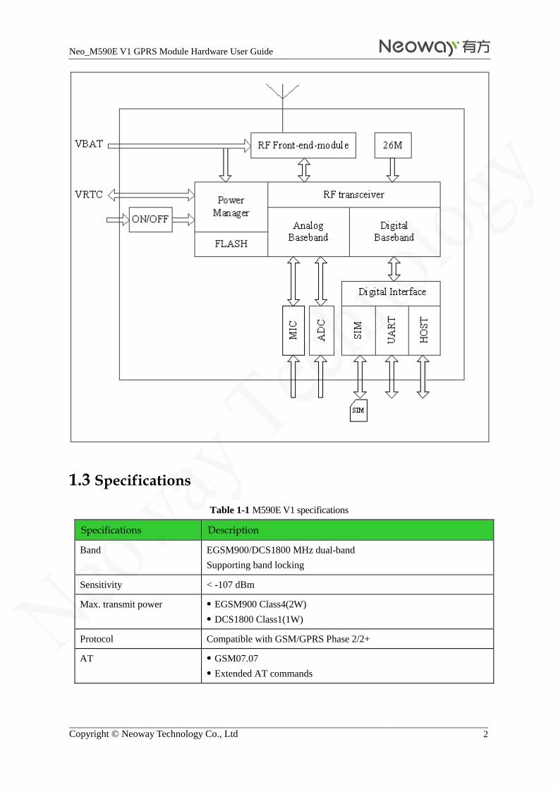
1.2 Block Diagram
The M590E V1 module consists of baseband controller, Flash ROM, RF section, application interfaces,
etc. All sections coordinate with each other to provide such communication functions as GPRS data and
voice.
The following figure shows the block diagram of M590E V1.
Neo_M590E V1 GPRS Module Hardware User Guide
Copyright © Neoway Technology Co., Ltd 2
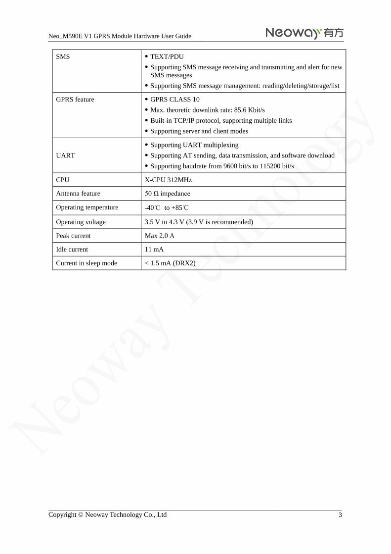
1.3 Specifications
Table 1-1 M590E V1 specifications
Specifications Description
Band EGSM900/DCS1800 MHz dual-band
Supporting band locking
Sensitivity < -107 dBm
Max. transmit power EGSM900 Class4(2W)
DCS1800 Class1(1W)
Protocol Compatible with GSM/GPRS Phase 2/2+
AT GSM07.07
Extended AT commands
Neo_M590E V1 GPRS Module Hardware User Guide
Copyright © Neoway Technology Co., Ltd 3
SMS TEXT/PDU
Supporting SMS message receiving and transmitting and alert for new
SMS messages
Supporting SMS message management: reading/deleting/storage/list
GPRS feature GPRS CLASS 10
Max. theoretic downlink rate: 85.6 Kbit/s
Built-in TCP/IP protocol, supporting multiple links
Supporting server and client modes
UART
Supporting UART multiplexing
Supporting AT sending, data transmission, and software download
Supporting baudrate from 9600 bit/s to 115200 bit/s
CPU X-CPU 312MHz
Antenna feature 50 Ω impedance
Operating temperature -40℃ to +85℃
Operating voltage 3.5 V to 4.3 V (3.9 V is recommended)
Peak current Max 2.0 A
Idle current 11 mA
Current in sleep mode < 1.5 mA (DRX2)
Neo_M590E V1 GPRS Module Hardware User Guide
Copyright © Neoway Technology Co., Ltd 4
2 Pin Description and PCB Foot Print
2.1 Specifications and Encapsulation
Specifications M590E V1
Dimensions 27.6 mm x 21.6 mm x 2.6 mm (H x W x D)
Weight 2.7 g
Encapsulation 27-pin LGA
Figure 2-1 Top view of the M590E V1 module
1
2
3
4
5
6
7
8
9
10 11
12
13
14
15
16
17
18
19
20
21
GND
VBAT
VBAT
GND
LIGHT
VDD_EXT
URXD
UTXD
DTR
RING SIM_DATA
SIM_CLK
SIM_RST
VSIM
GND
ADC_IN
NC
RESET
ON/OFF
GND
GPRS_ANT
Power GND
SIM
UART ADC
ANT Other
M590E V1
Top View
22 23 24 25 26 27
MIC
_P
MIC
_N
HO
ST
_R
X
HO
ST
_T
X
GN
D
NC

Neo_M590E V1 GPRS Module Hardware User Guide
Copyright © Neoway Technology Co., Ltd 5
2.2 Pin Definition
Table 2-1 M590E V1 pin definition
Pin Name I/O Function Reset Status
Level Feature (V)
Remarks
Power Supply and Switch Interfaces
2, 3 VBAT P Main power supply
input
3.5 V to 4.3 V (3.9
V is recommended)
6 VDD_EXT P 2.8 V power supply
output
Supply power for IO
level shifting circuit.
Load capability: less
than 50 mA
1, 4,
15, 20,
26
GND P Ground
19 ON/OFF DI On/Off input 0<VIL<0.6
2.1<VIH<VBAT
Low-level pulse can
change the On/Off
state.
18 RESET DI Reset input 0<VIL<0.6
2.1<VIH<3.1 Low level reset
UART Interface
7 URXD DI UART data receive I/PU
0<VIL<0.6
2.1<VIH<3.1
0<VOL<0.42
2.38<VOH<2.8
With 47K pull-up
inside 8 UTXD DO
UART data
transmit
24 HOST_RX DI HOST data receive Used for module
upgrade 25 HOST_TX DO HOST data
transmit
SIM Card
11 SIM_DATA DI/O SIM card data IO
0<VIL<0.25*VSI
M,
0.75*VSIM<VIH
<VSIM
0<VOL<0.15*VS
IM
0.85*VSIM<VOH
<VSIM
Compatible with
1.8/3.0 V SIM card
12 SIM_CLK DO SIM card clock
output
13 SIM_RST DO SIM card reset
output
14 VSIM P SIM card power
supply output
LED Indicators
5 LIGHT DO Status LED I/PD 2.8 V/4 mA output
SMS and Incoming Call Ring
10 RING DO Ring output I/PD Output 2.8V/4mA
Neo_M590E V1 GPRS Module Hardware User Guide
Copyright © Neoway Technology Co., Ltd 6
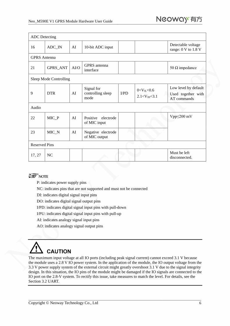
ADC Detecting
16 ADC_IN AI 10-bit ADC input Detectable voltage
range: 0 V to 1.8 V
GPRS Antenna
21 GPRS_ANT AI/O GPRS antenna
interface 50 Ω impedance
Sleep Mode Controlling
9 DTR AI
Signal for
controlling sleep
mode
I/PD 0<VIL<0.6
2.1<VIH<3.1
Low level by default
Used together with
AT commands
Audio
22 MIC_P AI Positive electrode
of MIC input
Vpp≤200 mV
23 MIC_N AI Negative electrode
of MIC output
Reserved Pins
17, 27 NC Must be left
disconnected.
P: indicates power supply pins
NC: indicates pins that are not supported and must not be connected
DI: indicates digital signal input pins
DO: indicates digital signal output pins
I/PD: indicates digital signal input pins with pull-down
I/PU: indicates digital signal input pins with pull-up
AI: indicates analogy signal input pins
AO: indicates analogy signal output pins
The maximum input voltage at all IO ports (including peak signal current) cannot exceed 3.1 V because
the module uses a 2.8 V IO power system. In the application of the module, the IO output voltage from the
3.3 V power supply system of the external circuit might greatly overshoot 3.1 V due to the signal integrity
design. In this situation, the IO pins of the module might be damaged if the IO signals are connected to the
IO port on the 2.8-V system. To rectify this issue, take measures to match the level. For details, see the
Section 3.2 UART.
Neo_M590E V1 GPRS Module Hardware User Guide
Copyright © Neoway Technology Co., Ltd 7
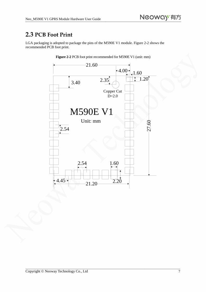
2.3 PCB Foot Print
LGA packaging is adopted to package the pins of the M590E V1 module. Figure 2-2 shows the
recommended PCB foot print.
Figure 2-2 PCB foot print recommended for M590E V1 (unit: mm)
21.20
27.6
0
21.60
3.40
4.00
2.35
M590E V1Unit: mm
Copper Cut
D=2.0
4.45 2.20
1.60
2.54
2.54
1.20
1.60
Neo_M590E V1 GPRS Module Hardware User Guide
Copyright © Neoway Technology Co., Ltd 8
3 Interface Design
3.1 Power Supply and Switch Interfaces
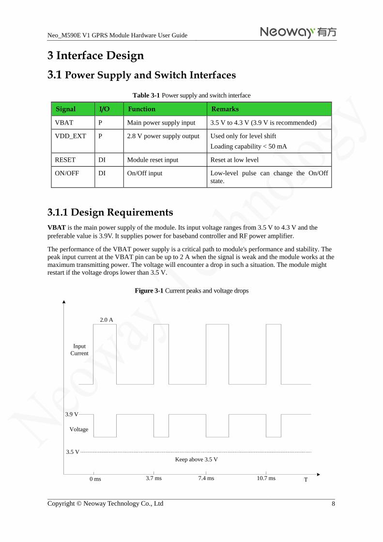
Table 3-1 Power supply and switch interface
Signal I/O Function Remarks
VBAT P Main power supply input 3.5 V to 4.3 V (3.9 V is recommended)
VDD_EXT P 2.8 V power supply output Used only for level shift
Loading capability < 50 mA
RESET DI Module reset input Reset at low level
ON/OFF DI On/Off input Low-level pulse can change the On/Off
state.
3.1.1 Design Requirements
VBAT is the main power supply of the module. Its input voltage ranges from 3.5 V to 4.3 V and the
preferable value is 3.9V. It supplies power for baseband controller and RF power amplifier.
The performance of the VBAT power supply is a critical path to module's performance and stability. The
peak input current at the VBAT pin can be up to 2 A when the signal is weak and the module works at the
maximum transmitting power. The voltage will encounter a drop in such a situation. The module might
restart if the voltage drops lower than 3.5 V.
Figure 3-1 Current peaks and voltage drops
Keep above 3.5 VKeep above 3.5 V3.5 V3.5 V
0 ms0 ms 3.7 ms3.7 ms 7.4 ms7.4 ms 10.7 ms10.7 ms TT
2.0 A2.0 A
VoltageVoltage
Input
Current
Input
Current
3.9 V3.9 V
Neo_M590E V1 GPRS Module Hardware User Guide
Copyright © Neoway Technology Co., Ltd 9
Figure 3-2 shows a recommended power supply design for the module.
Figure 3-2 Capacitors used for the power supply
Power Supply GPRS Module
Close to the pin of the module
D1 C1 C2 C3 C4
VBATCurrent testing point
I_max
C5
In the circuit, you can use TVS at D1 to enhance the performance of the module during a burst.
SMF5.0AG (Vrwm=5V&Pppm=200W) is recommended. A large bypass tantalum capacitor (220 μF or
100 μF) or aluminum capacitor (470 μF or 1000 μF) is expected at C1 to reduce voltage drops during
bursts together with C2 (10 μF capacitor). In addition, you need to add 0.1 μF, 100 pF, and 33 pF filter
capacitors to enhance the stability of the power supply.
A controllable power supply is preferable if used in harsh conditions. The module might fail to reset in
remote or unattended applications, or in an environment with great electromagnetic interference (EMI).
You can use the EN pin on the LDO or DC/DC chipset to control the switch of the power supply as shown
in Figure 3-3.
MIC29302WU in the following figure is an LDO and outputs 3 A current to ensure the performance of the
module.
Figure 3-3 Reference design of power supply control
The alternative way is to use a p-MOSFET to control the module's power, as shown in Figure 3-4. When
the external MCU detects the exceptions such as no response from the module or the disconnection of
GPRS, power off/on can rectify the module exceptions. In Figure 3-4, the module is powered on when
GPRS_EN is set to high level.
VCC_IN_5V
GPRS_EN VBAT
100 uF
TAN
0.1 uF
TVS
5V10 uF470uF
TAN
10K
4.75K
VOUT
MIC29302WU
EN
VIN ADJ
0.1 uF 100pF 33pF

Neo_M590E V1 GPRS Module Hardware User Guide
Copyright © Neoway Technology Co., Ltd 10
Figure 3-4 Reference design of power supply controlled by p-MOSFET
Q2 is added to eliminate the need for a high enough voltage level of the host GPIO. In case that the GPIO
can output a high voltage greater than VCC_IN_3.9V - |VGS(th)|, where VGS(th) is the Gate Threshold
Voltage, Q2 is not needed.
Reference components:
Q1 can be IRML6401 or Rds(on) p-MOSFET which has higher withstand voltage and drain current.
Q2: a common NPN transistor, e.g. MMBT3904; or a digital NPN transistor, e.g. DTC123. If digital
transistor is used, delete R1 and R2.
C3: 470 uF tantalum capacitor rated at 6.3V; or 1000 uF aluminum capacitor. If lithium battery is used to
supply power, C3 can be 220 uF tantalum capacitor.
Protection
Place a TVS diode (VRWM=5 V) on the VBAT power supply to ground, especially in automobile
applications. For some stable power supplies, zener diodes can decrease the power supply overshoot.
MMSZ5231B1T1G from ONSEMI and PZ3D4V2 from Prisemi are options.
Trace
The trace width of primary loop lines for VBAT on PCB must be able to support the safe transmission of
2A current and ensure no obvious loop voltage decrease. Therefore, the trace width of VBAT loop line is
required 2 mm and the ground should be as complete as possible.
Separation
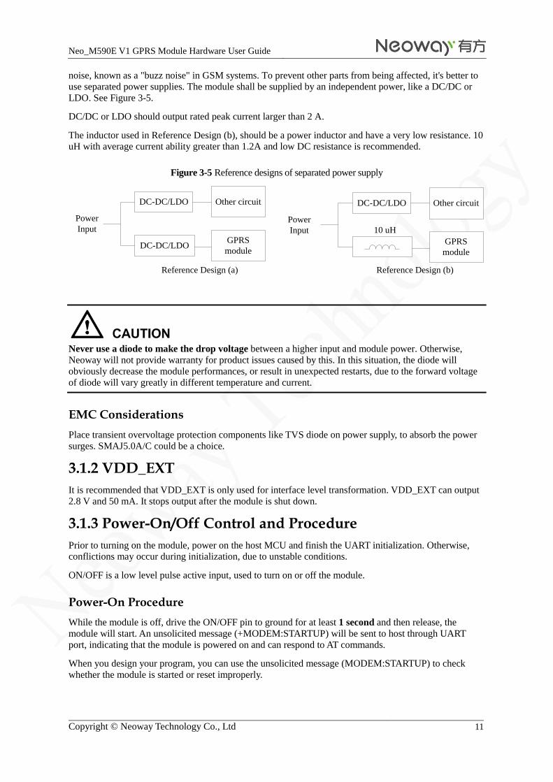
As shown in Figure 3-1, the GPRS module works in burst mode that generates voltage drops on power
supply. Furthermore, this results in a 217 Hz TDD noise through power (One of the way generating noise.
Another way is through RF radiation). Analog parts, especially the audio circuits, are subjected to this
Neo_M590E V1 GPRS Module Hardware User Guide
Copyright © Neoway Technology Co., Ltd 11
noise, known as a "buzz noise" in GSM systems. To prevent other parts from being affected, it's better to
use separated power supplies. The module shall be supplied by an independent power, like a DC/DC or
LDO. See Figure 3-5.
DC/DC or LDO should output rated peak current larger than 2 A.
The inductor used in Reference Design (b), should be a power inductor and have a very low resistance. 10
uH with average current ability greater than 1.2A and low DC resistance is recommended.
Figure 3-5 Reference designs of separated power supply
Other circuitDC-DC/LDO
GPRS
moduleDC-DC/LDO
Power
Input
Other circuitDC-DC/LDO
GPRS
module
Power
Input 10 uH
Reference Design (a) Reference Design (b)
Never use a diode to make the drop voltage between a higher input and module power. Otherwise,
Neoway will not provide warranty for product issues caused by this. In this situation, the diode will
obviously decrease the module performances, or result in unexpected restarts, due to the forward voltage
of diode will vary greatly in different temperature and current.
EMC Considerations
Place transient overvoltage protection components like TVS diode on power supply, to absorb the power
surges. SMAJ5.0A/C could be a choice.
3.1.2 VDD_EXT
It is recommended that VDD_EXT is only used for interface level transformation. VDD_EXT can output
2.8 V and 50 mA. It stops output after the module is shut down.
3.1.3 Power-On/Off Control and Procedure
Prior to turning on the module, power on the host MCU and finish the UART initialization. Otherwise,
conflictions may occur during initialization, due to unstable conditions.
ON/OFF is a low level pulse active input, used to turn on or off the module.
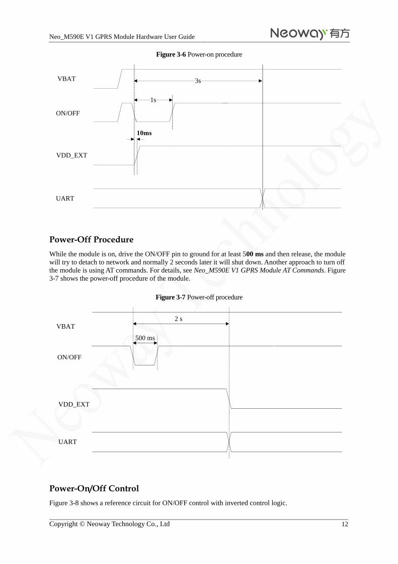
Power-On Procedure
While the module is off, drive the ON/OFF pin to ground for at least 1 second and then release, the
module will start. An unsolicited message (+MODEM:STARTUP) will be sent to host through UART
port, indicating that the module is powered on and can respond to AT commands.
When you design your program, you can use the unsolicited message (MODEM:STARTUP) to check
whether the module is started or reset improperly.
Neo_M590E V1 GPRS Module Hardware User Guide
Copyright © Neoway Technology Co., Ltd 12
Figure 3-6 Power-on procedure
Power-Off Procedure
While the module is on, drive the ON/OFF pin to ground for at least 500 ms and then release, the module
will try to detach to network and normally 2 seconds later it will shut down. Another approach to turn off
the module is using AT commands. For details, see Neo_M590E V1 GPRS Module AT Commands. Figure
3-7 shows the power-off procedure of the module.
Figure 3-7 Power-off procedure
Power-On/Off Control
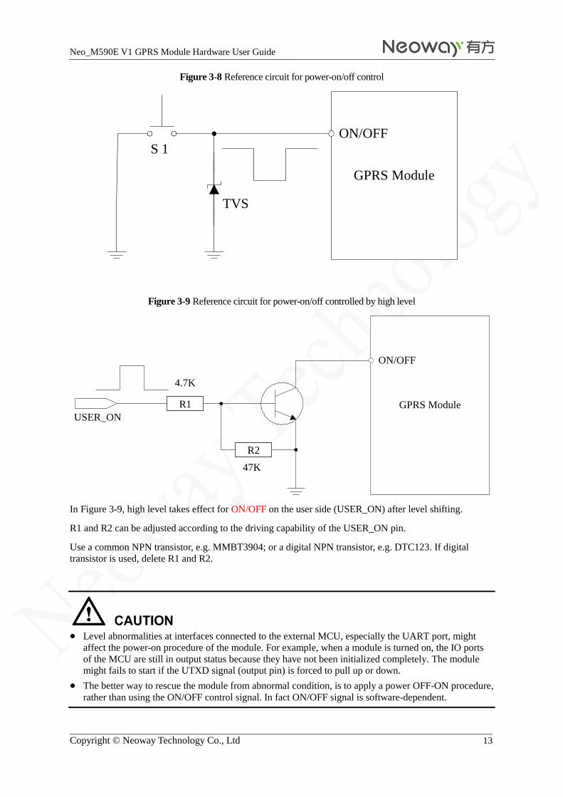
Figure 3-8 shows a reference circuit for ON/OFF control with inverted control logic.
VBAT
ON/OFF
VDD_EXT
UART
1s
3s
10ms
VBAT
ON/OFF
VDD_EXT
UART
2 s
500 ms
Neo_M590E V1 GPRS Module Hardware User Guide
Copyright © Neoway Technology Co., Ltd 13
Figure 3-8 Reference circuit for power-on/off control
Figure 3-9 Reference circuit for power-on/off controlled by high level
In Figure 3-9, high level takes effect for ON/OFF on the user side (USER_ON) after level shifting.
R1 and R2 can be adjusted according to the driving capability of the USER_ON pin.
Use a common NPN transistor, e.g. MMBT3904; or a digital NPN transistor, e.g. DTC123. If digital
transistor is used, delete R1 and R2.
Level abnormalities at interfaces connected to the external MCU, especially the UART port, might
affect the power-on procedure of the module. For example, when a module is turned on, the IO ports
of the MCU are still in output status because they have not been initialized completely. The module
might fails to start if the UTXD signal (output pin) is forced to pull up or down.
The better way to rescue the module from abnormal condition, is to apply a power OFF-ON procedure,
rather than using the ON/OFF control signal. In fact ON/OFF signal is software-dependent.
GPRS Module
ON/OFF
TVS
S 1
USER_ON
GPRS Module
ON/OFF
4.7K
47K
R1
R2

Neo_M590E V1 GPRS Module Hardware User Guide
Copyright © Neoway Technology Co., Ltd 14
3.1.4 RESET
You can reset the module by keeping the RESET pin low level for more than 100 ms. The pin is pulled up
by an internal resistor and the typical high level is 2.8 V. The RESET pin can be left disconnected if not
used. If you use 3.3 V IO system, you are advised to separate it by using triode. Please refer to Figure 3-
10.
Figure 3-10 Reset circuit with triode separating
3.2 UART
Table 3-2 UART
Pin No. Signal I/O Function Description Remarks
7 URXD DI UART data receive Internal 47K pullup
8 UTXD DO UART data transmit
24 HOST_RX DI UART data receive
25 HOST_TX DO UART data transmit
UART is used for AT commands. Figure 3-11 shows the signal connection between the module (DCE) and
the terminal (DTE).
Figure 3-11 Signal connection between DCE and DTE
RESET
VDD_EXT
4.7K
47KGPRS Module
DCE
URXD
UTXD
DTE
UTXD
URXD
Neo_M590E V1 GPRS Module Hardware User Guide
Copyright © Neoway Technology Co., Ltd 15
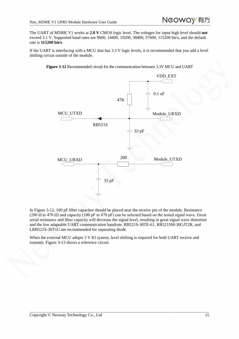
The UART of M590E V1 works at 2.8 V CMOS logic level. The voltages for input high level should not
exceed 3.1 V. Supported baud rates are 9600, 14400, 19200, 38400, 57600, 115200 bit/s, and the default
rate is 115200 bit/s.
If the UART is interfacing with a MCU that has 3.3 V logic levels, it is recommended that you add a level
shifting circuit outside of the module.
Figure 3-12 Recommended circuit for the communication between 3.3V MCU and UART
In Figure 3-12, 100 pF filter capacitor should be placed near the receive pin of the module. Resistance
(200 Ω to 470 Ω) and capacity (100 pF to 470 pF) can be selected based on the tested signal wave. Great
serial resistance and filter capacity will decrease the signal level, resulting in great signal wave distortion
and the low adaptable UART communication baudrate. RB521S-30TE-61, RB521SM-30GJT2R, and
LRB521S-30T1G are recommended for separating diode.
When the external MCU adopts 5 V IO system, level shifting is required for both UART receive and
transmit. Figure 3-13 shows a reference circuit.
Module_URXD
Module_UTXD
VDD_EXT
0.1 uF
47K
RB521S
200
33 pF
33 pF
MCU_UTXD
MCU_URXD
Neo_M590E V1 GPRS Module Hardware User Guide
Copyright © Neoway Technology Co., Ltd 16
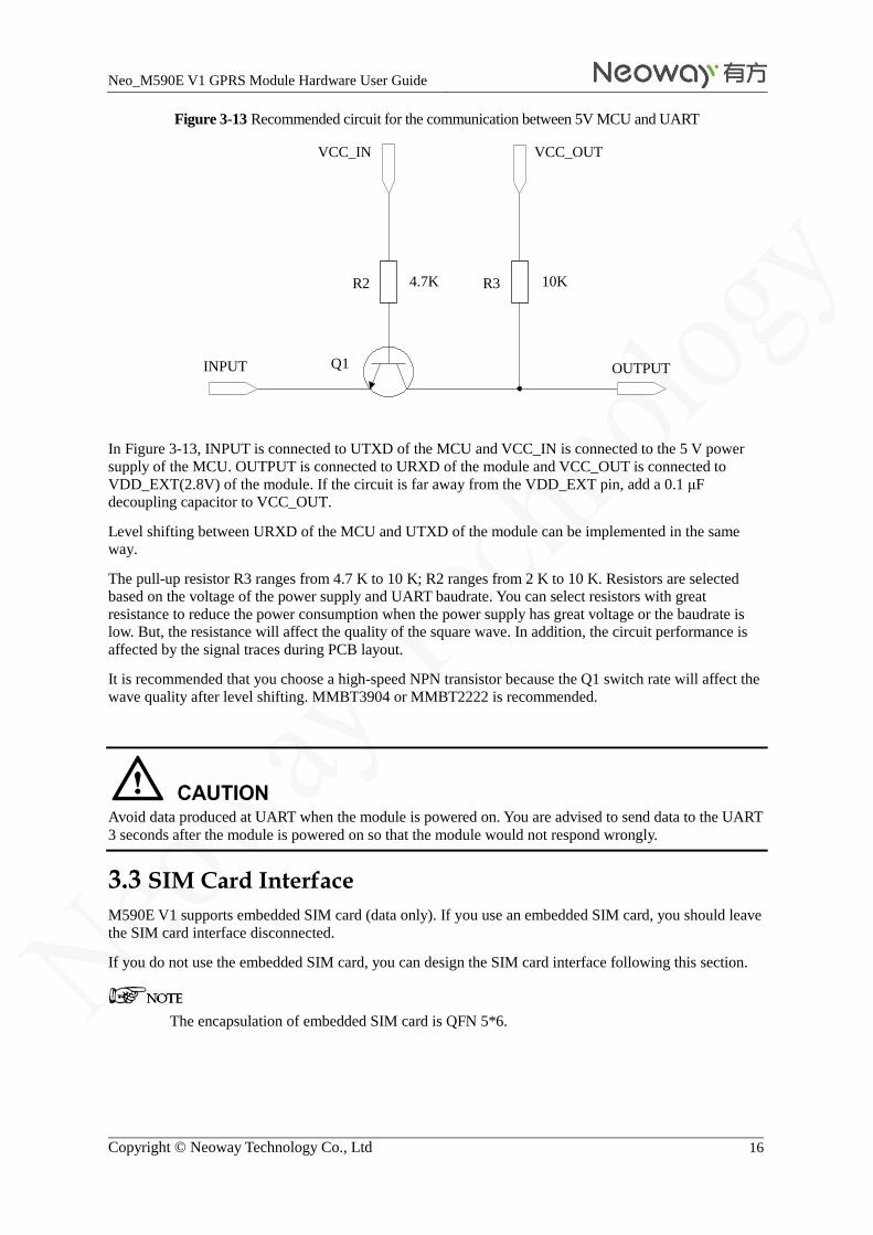
Figure 3-13 Recommended circuit for the communication between 5V MCU and UART
In Figure 3-13, INPUT is connected to UTXD of the MCU and VCC_IN is connected to the 5 V power
supply of the MCU. OUTPUT is connected to URXD of the module and VCC_OUT is connected to
VDD_EXT(2.8V) of the module. If the circuit is far away from the VDD_EXT pin, add a 0.1 μF
decoupling capacitor to VCC_OUT.
Level shifting between URXD of the MCU and UTXD of the module can be implemented in the same
way.
The pull-up resistor R3 ranges from 4.7 K to 10 K; R2 ranges from 2 K to 10 K. Resistors are selected
based on the voltage of the power supply and UART baudrate. You can select resistors with great
resistance to reduce the power consumption when the power supply has great voltage or the baudrate is
low. But, the resistance will affect the quality of the square wave. In addition, the circuit performance is
affected by the signal traces during PCB layout.
It is recommended that you choose a high-speed NPN transistor because the Q1 switch rate will affect the
wave quality after level shifting. MMBT3904 or MMBT2222 is recommended.
Avoid data produced at UART when the module is powered on. You are advised to send data to the UART
3 seconds after the module is powered on so that the module would not respond wrongly.
3.3 SIM Card Interface
M590E V1 supports embedded SIM card (data only). If you use an embedded SIM card, you should leave
the SIM card interface disconnected.
If you do not use the embedded SIM card, you can design the SIM card interface following this section.
The encapsulation of embedded SIM card is QFN 5*6.
INPUT OUTPUT
VCC_IN VCC_OUT
4.7K 10K
Q1
R2 R3
Neo_M590E V1 GPRS Module Hardware User Guide
Copyright © Neoway Technology Co., Ltd 17
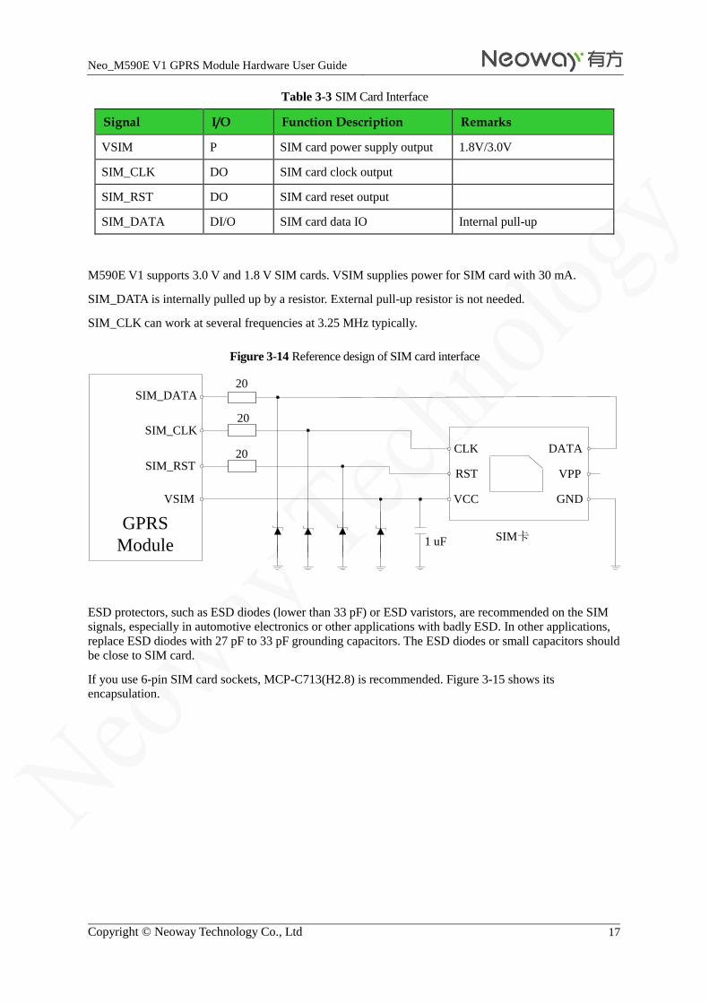
Table 3-3 SIM Card Interface
Signal I/O Function Description Remarks
VSIM P SIM card power supply output 1.8V/3.0V
SIM_CLK DO SIM card clock output
SIM_RST DO SIM card reset output
SIM_DATA DI/O SIM card data IO Internal pull-up
M590E V1 supports 3.0 V and 1.8 V SIM cards. VSIM supplies power for SIM card with 30 mA.
SIM_DATA is internally pulled up by a resistor. External pull-up resistor is not needed.
SIM_CLK can work at several frequencies at 3.25 MHz typically.
Figure 3-14 Reference design of SIM card interface
ESD protectors, such as ESD diodes (lower than 33 pF) or ESD varistors, are recommended on the SIM
signals, especially in automotive electronics or other applications with badly ESD. In other applications,
replace ESD diodes with 27 pF to 33 pF grounding capacitors. The ESD diodes or small capacitors should
be close to SIM card.
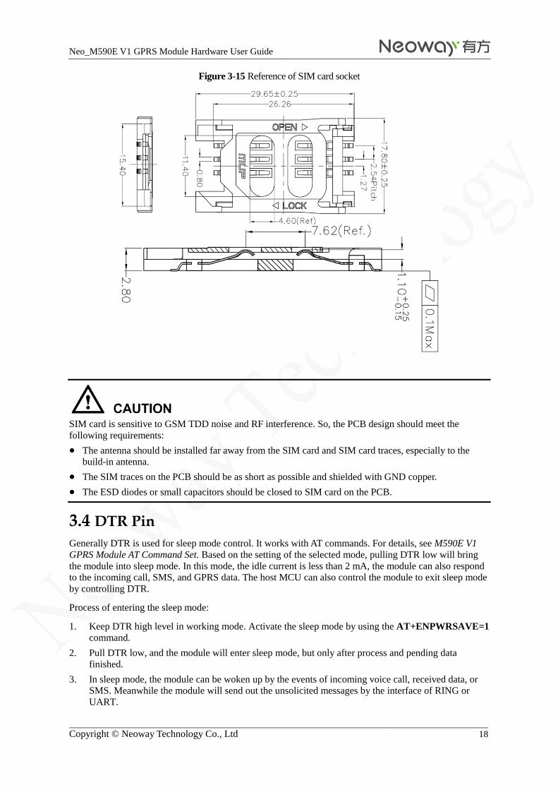
If you use 6-pin SIM card sockets, MCP-C713(H2.8) is recommended. Figure 3-15 shows its
encapsulation.
20
20
20
1 uF
SIM_DATA
SIM_CLK
SIM_RST
VSIM
GPRS
Module
CLK
RST
VCC
VPP
GND
SIM卡
DATA
Neo_M590E V1 GPRS Module Hardware User Guide
Copyright © Neoway Technology Co., Ltd 18
Figure 3-15 Reference of SIM card socket
SIM card is sensitive to GSM TDD noise and RF interference. So, the PCB design should meet the
following requirements:
The antenna should be installed far away from the SIM card and SIM card traces, especially to the
build-in antenna.
The SIM traces on the PCB should be as short as possible and shielded with GND copper.
The ESD diodes or small capacitors should be closed to SIM card on the PCB.
3.4 DTR Pin
Generally DTR is used for sleep mode control. It works with AT commands. For details, see M590E V1
GPRS Module AT Command Set. Based on the setting of the selected mode, pulling DTR low will bring
the module into sleep mode. In this mode, the idle current is less than 2 mA, the module can also respond
to the incoming call, SMS, and GPRS data. The host MCU can also control the module to exit sleep mode
by controlling DTR.
Process of entering the sleep mode:
1. Keep DTR high level in working mode. Activate the sleep mode by using the AT+ENPWRSAVE=1
command.
2. Pull DTR low, and the module will enter sleep mode, but only after process and pending data
finished.
3. In sleep mode, the module can be woken up by the events of incoming voice call, received data, or
SMS. Meanwhile the module will send out the unsolicited messages by the interface of RING or
UART.
Neo_M590E V1 GPRS Module Hardware User Guide
Copyright © Neoway Technology Co., Ltd 19
Upon receipt of the unsolicited messages, the host MCU should pull DTR high firstly, otherwise the
module will resume sleep mode shortly. Then the host MCU can process the voice call, received data,
or SMS. After processing is finished, pull DTR low again to put the module into sleep mode.
4. Pull DTR high, the module will exit from sleep mode actively, and furthermore enable the UART.
Thus the voice call, received data, or SMS can be processed through UART. After processing
finished pull it low again, to take the module back to sleep mode.
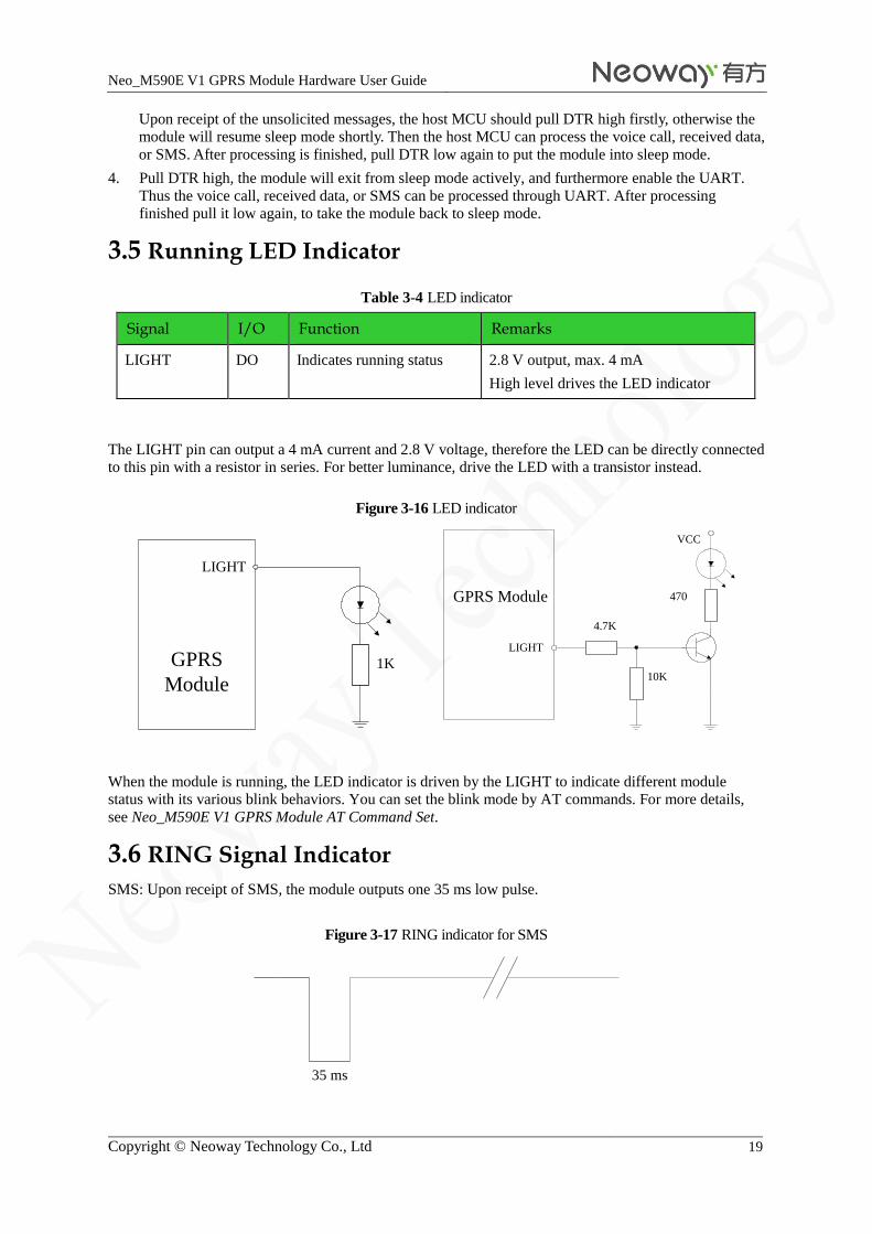
3.5 Running LED Indicator
Table 3-4 LED indicator
Signal I/O Function Remarks
LIGHT DO Indicates running status 2.8 V output, max. 4 mA
High level drives the LED indicator
The LIGHT pin can output a 4 mA current and 2.8 V voltage, therefore the LED can be directly connected
to this pin with a resistor in series. For better luminance, drive the LED with a transistor instead.
Figure 3-16 LED indicator
When the module is running, the LED indicator is driven by the LIGHT to indicate different module
status with its various blink behaviors. You can set the blink mode by AT commands. For more details,
see Neo_M590E V1 GPRS Module AT Command Set.
3.6 RING Signal Indicator
SMS: Upon receipt of SMS, the module outputs one 35 ms low pulse.
Figure 3-17 RING indicator for SMS
LIGHT
GPRS
Module1K
LIGHT
GPRS Module
10K
VCC
470
4.7K
35 ms
Neo_M590E V1 GPRS Module Hardware User Guide
Copyright © Neoway Technology Co., Ltd 20
3.7 RF Interface
3.7.1 RF Design and PCB Layout
A 50 Ω antenna is required. VSWR ranges from 1.1 to 1.5. The antenna should be well matched to
achieve best performance. It should be installed far away from high speed logic circuits, DC/DC power, or
any other strong disturbing sources.
For multiple-layer PCB, the trace between the antenna pad of module and the antenna connector, should
have a 50 Ω characteristic impedance, and be as short as possible. The trace should be surrounded by
ground copper. Place plenty of via holes to connect this ground copper to main ground plane, at the copper
edge.
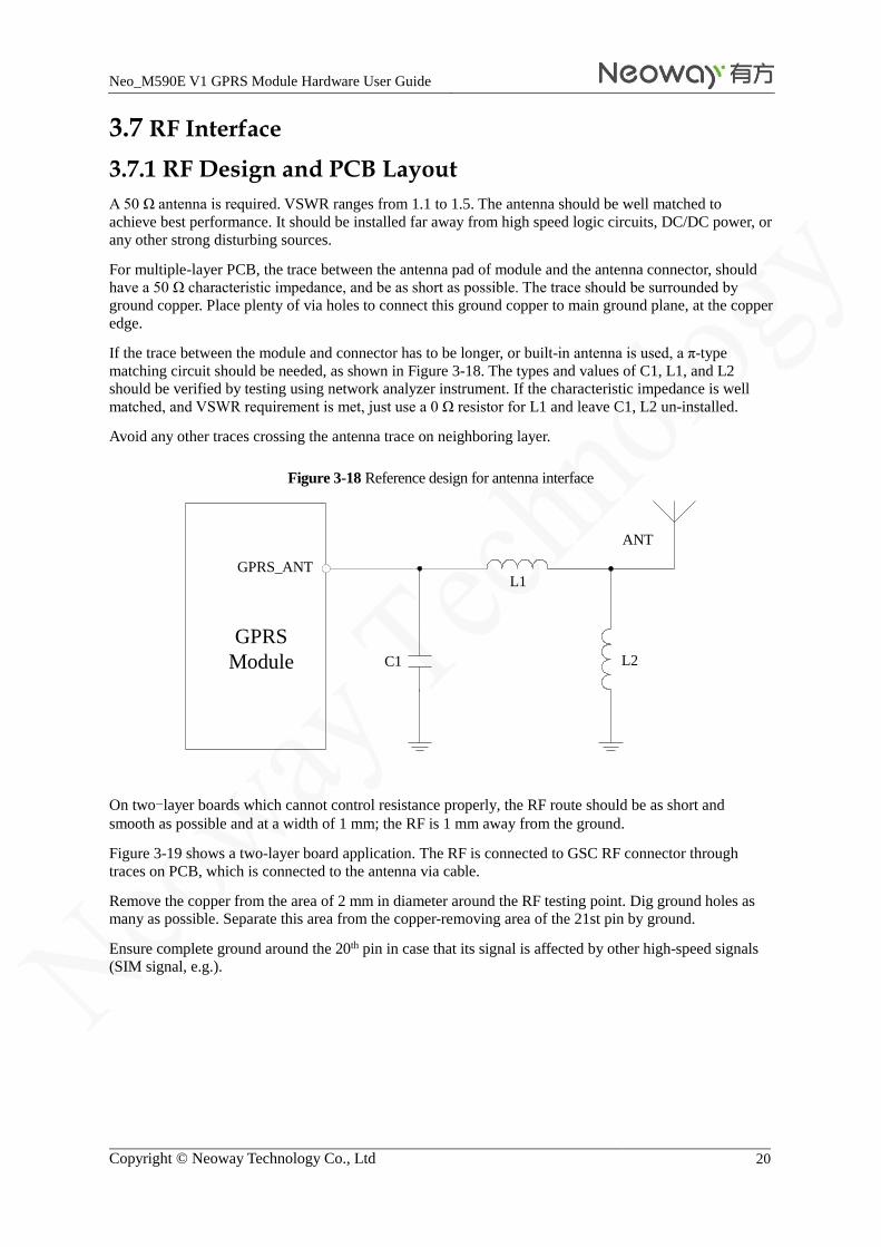
If the trace between the module and connector has to be longer, or built-in antenna is used, a π-type
matching circuit should be needed, as shown in Figure 3-18. The types and values of C1, L1, and L2
should be verified by testing using network analyzer instrument. If the characteristic impedance is well
matched, and VSWR requirement is met, just use a 0 Ω resistor for L1 and leave C1, L2 un-installed.
Avoid any other traces crossing the antenna trace on neighboring layer.
Figure 3-18 Reference design for antenna interface
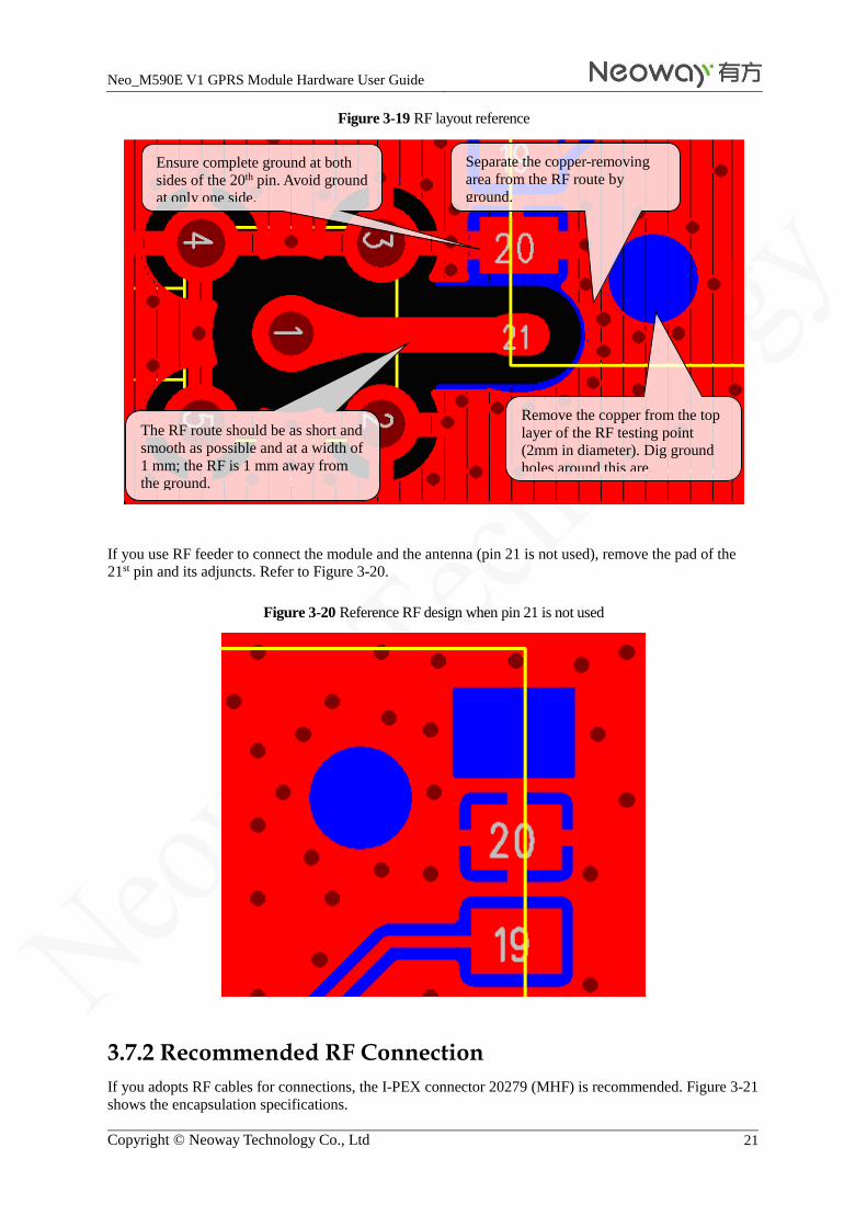
On two-layer boards which cannot control resistance properly, the RF route should be as short and
smooth as possible and at a width of 1 mm; the RF is 1 mm away from the ground.
Figure 3-19 shows a two-layer board application. The RF is connected to GSC RF connector through
traces on PCB, which is connected to the antenna via cable.
Remove the copper from the area of 2 mm in diameter around the RF testing point. Dig ground holes as
many as possible. Separate this area from the copper-removing area of the 21st pin by ground.
Ensure complete ground around the 20th pin in case that its signal is affected by other high-speed signals
(SIM signal, e.g.).
GPRS
Module
ANT
C1
GPRS_ANT
L2
L1
Neo_M590E V1 GPRS Module Hardware User Guide
Copyright © Neoway Technology Co., Ltd 21
Figure 3-19 RF layout reference
If you use RF feeder to connect the module and the antenna (pin 21 is not used), remove the pad of the
21st pin and its adjuncts. Refer to Figure 3-20.
Figure 3-20 Reference RF design when pin 21 is not used
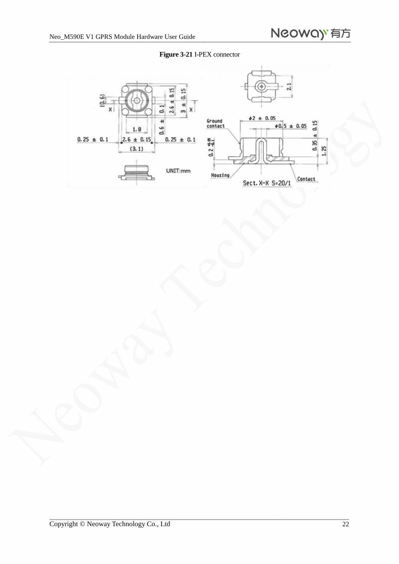
3.7.2 Recommended RF Connection
If you adopts RF cables for connections, the I-PEX connector 20279 (MHF) is recommended. Figure 3-21
shows the encapsulation specifications.
Ensure complete ground at both
sides of the 20th pin. Avoid ground
at only one side.
The RF route should be as short and
smooth as possible and at a width of
1 mm; the RF is 1 mm away from
the ground.
Separate the copper-removing
area from the RF route by
ground.
Remove the copper from the top
layer of the RF testing point
(2mm in diameter). Dig ground
holes around this are.
Neo_M590E V1 GPRS Module Hardware User Guide
Copyright © Neoway Technology Co., Ltd 22
Figure 3-21 I-PEX connector
Neo_M590E V1 GPRS Module Hardware User Guide
Copyright © Neoway Technology Co., Ltd 23
4 Electric Features and Reliability
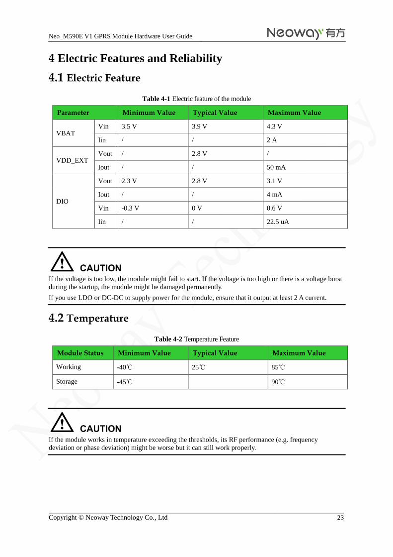
4.1 Electric Feature
Table 4-1 Electric feature of the module
Parameter Minimum Value Typical Value Maximum Value
VBAT Vin 3.5 V 3.9 V 4.3 V
Iin / / 2 A
VDD_EXT Vout / 2.8 V /
Iout / / 50 mA
DIO
Vout 2.3 V 2.8 V 3.1 V
Iout / / 4 mA
Vin -0.3 V 0 V 0.6 V
Iin / / 22.5 uA
If the voltage is too low, the module might fail to start. If the voltage is too high or there is a voltage burst
during the startup, the module might be damaged permanently.
If you use LDO or DC-DC to supply power for the module, ensure that it output at least 2 A current.
4.2 Temperature
Table 4-2 Temperature Feature
Module Status Minimum Value Typical Value Maximum Value
Working -40℃ 25℃ 85℃
Storage -45℃ 90℃
If the module works in temperature exceeding the thresholds, its RF performance (e.g. frequency
deviation or phase deviation) might be worse but it can still work properly.

Neo_M590E V1 GPRS Module Hardware User Guide
Copyright © Neoway Technology Co., Ltd 24
4.3 Current
Table 4-3 Current feature
Parameter Testing Conditions Testing Result (Average Current)
Testing voltage 3.9 V Agilent power supply /
Off leakage current Power on the module or use AT command to shut
the module down. 190 μA
Idle mode Set the instrument and power on the module. 11 mA
Sleep mode Set the instrument properly (DRX=5) 1.5mA
Average network
searching current
Set the instrument.
Start the module. Wait until the module registers
the instrument.
35 mA
Voice service Maximum power level in full rate
mode
EGSM900 220 mA
DCS1800 155 mA
GPRS class 12
2Up/3Down@Gamma=3 EGSM900 350 mA
DCS1800 230 mA
1Up/4Down@Gamma=3 EGSM900 224 mA
DCS1800 160 mA
The data in the above table is typical values obtained during tests in lab. It might be a little bit different in
manufacturing. Also, the test results might be various due to different settings or testing methods.
4.4 ESD Protection
Electronics need to pass sever ESD tests. The following table shows the ESD capability of key pins of our
module. It is recommended that you add ESD protection to those pins in accordance to the application to
ensure your product quality when designing your products.
Humility: 45%
Temperature: 25℃
Table 4-4 ESD feature of the module
Testing Point Contact Discharge Air Discharge
VBAT ±8 KV ±15 KV
GND ±8 KV ±15 KV
ANT ±8 KV ±15 KV
Neo_M590E V1 GPRS Module Hardware User Guide
Copyright © Neoway Technology Co., Ltd 25
Cover ±8 KV ±15 KV
URXD/UTXD ±4 KV ±8 KV
Others ±4 KV ±8 KV

Neo_M590E V1 GPRS Module Hardware User Guide
Copyright © Neoway Technology Co., Ltd 26
5 RF Features
5.1 Work Band
Table 5-1 Work band
Work Band Uplink Downlink
EGSM900 880~915 MHz 925~960 MHz
DCS1800 1710~1785 MHz 1805~1880 MHz
5.2 Transmitting Power and Receiving Sensitivity
5.2.1 Transmitting Power
Table 5-2 Transmitting power (EGSM900)
PCL Transmitting Power Threshold Range
5 33 dBm ±2 dBm
6 31 dBm ±3 dBm
7 29 dBm ±3 dBm
8 27 dBm ±3 dBm
9 25 dBm ±3 dBm
10 23 dBm ±3 dBm
11 21 dBm ±3 dBm
12 19 dBm ±3 dBm
13 17 dBm ±3 dBm
14 15 dBm ±3 dBm
15 13 dBm ±5 dBm
16 11 dBm ±5 dBm
17 9 dBm ±5 dBm
18 7 dBm ±5 dBm
19 5 dBm ±5 dBm
Table 5-3 Transmitting power (DCS1800)
PCL Transmitting Power Threshold Range
0 30 dBm ±2 dBm
1 28 dBm ±3 dBm

Neo_M590E V1 GPRS Module Hardware User Guide
Copyright © Neoway Technology Co., Ltd 27
2 26 dBm ±3 dBm
3 24 dBm ±3 dBm
4 22 dBm ±3 dBm
5 20 dBm ±3 dBm
6 18 dBm ±3 dBm
7 16 dBm ±3 dBm
8 14 dBm ±3 dBm
9 12 dBm ±3 dBm
10 10 dBm ±4 Bm
11 8 dBm ±4 Bm
12 6 dBm ±4 Bm
13 4 dBm ±4 dBm
14 2 dBm ±5 dBm
15 0 dBm ±5 dBm
5.2.2 Receiving Sensitivity
Band Typical
GSM800&EGSM900 <-107 dBm
DCS1800&PCS1900 <-107 dBm
The data in the above tables is obtained by connecting the module to RF test instrument (e.g.
CMU200, CWM500, or Agilent8960) in lab tests. It is for reference only.
Neo_M590E V1 GPRS Module Hardware User Guide
Copyright © Neoway Technology Co., Ltd 28
6 Mounting the Module onto the Application Board
M590E V1 is compatible with industrial standard reflow profile for lead-free SMT process.
The reflow profile is process dependent, so the following recommendation is just a start point guideline:
Only one flow is supported.
Quality of the solder joint depends on the solder volume. Minimum of 0.15 mm stencil thickness is
recommended.
Use bigger aperture size of the stencil than actual pad size.
Use a low-residue, no-clean type solder paste.
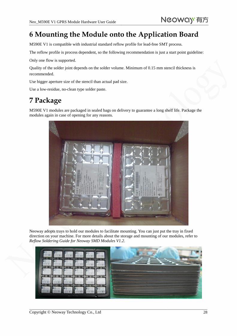
7 Package
M590E V1 modules are packaged in sealed bags on delivery to guarantee a long shelf life. Package the
modules again in case of opening for any reasons.
Neoway adopts trays to hold our modules to facilitate mounting. You can just put the tray in fixed
direction on your machine. For more details about the storage and mounting of our modules, refer to Reflow Soldering Guide for Neoway SMD Modules V1.2.
Neo_M590E V1 GPRS Module Hardware User Guide
Copyright © Neoway Technology Co., Ltd 29
8 Abbreviations
ADC Analog-Digital Converter
AFC Automatic Frequency Control
AGC Automatic Gain Control
AMR Acknowledged multirate (speech coder)
CSD Circuit Switched Data
CPU Central Processing Unit
DAI Digital Audio interface
DAC Digital-to-Analog Converter
DCE Data Communication Equipment
DSP Digital Signal Processor
DTE Data Terminal Equipment
DTMF Dual Tone Multi-Frequency
DTR Data Terminal Ready
EFR Enhanced Full Rate
EGSM Enhanced GSM
EMC Electromagnetic Compatibility
EMI Electro Magnetic Interference
ESD Electronic Static Discharge
ETS European Telecommunication Standard
FDMA Frequency Division Multiple Access
FR Full Rate
GPRS General Packet Radio Service
GSM Global Standard for Mobile Communications
HR Half Rate
IC Integrated Circuit
IMEI International Mobile Equipment Identity
LCD Liquid Crystal Display
LED Light Emitting Diode
MS Mobile Station
PCB Printed Circuit Board
PCS Personal Communication System
Neo_M590E V1 GPRS Module Hardware User Guide
Copyright © Neoway Technology Co., Ltd 30
RAM Random Access Memory
RF Radio Frequency
ROM Read-only Memory
RMS Root Mean Square
RTC Real Time Clock
SIM Subscriber Identification Module
SMS Short Message Service
SRAM Static Random Access Memory
TA Terminal adapter
TDMA Time Division Multiple Access
UART Universal asynchronous receiver-transmitter
VSWR Voltage Standing Wave Ratio