nehalem-ex: a 45nm, 8-core enterprise processor
TRANSCRIPT
1
Nehalem-EX: a 45nm, 8-core Enterprise Processor
Stefan RusuIntel CorporationSanta Clara, CA

2
Outline
• Process Technology• Processor Scaling Trends• Block Diagram and Die Photo• Cache Design• Core and Cache Recovery• Clock and Voltage Domains• Power, Package and Thermals• I/O Links• Idle Power Reduction• Summary

3
45nm Hi-k Metal Gate Technology
World’s first Hi-k Metal Gate CMOS transistors integrated with 3rd generation strained silicon
K. Mistry, IEDM 2007

4
Gate Leakage Reduction
HK+MG significantly reduces gate leakage
0.00001
0.0001
0.001
0.01
0.1
1
10
100
-1.2 -1 -0.8 -0.6 -0.4 -0.2 0 0.2 0.4 0.6 0.8 1 1.2
VGS (V)
Nor
mal
ized
Gat
e Le
akag
e SiON/Poly 65nm
HiK+MG 45nm
NMOS PMOS
HiK+MG 45nm
SiON/Poly 65nm
25x
1000x
K. Mistry, IEDM 2007
5
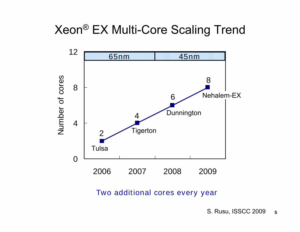
Xeon® EX Multi-Core Scaling Trend
Two additional cores every year
2
4
6
8
0
4
8
12
2006 2007 2008 2009
Num
ber
of c
ores
65nm 45nm
Tulsa
Tigerton
Dunnington
Nehalem-EX
S. Rusu, ISSCC 2009

6
Processor Block Diagram
• 8 cores, 16 threads, 2 integrated memory controllers• 4 point-to-point Quick Path Interconnect links• Two Scalable Memory Interfaces per memory controller• Two counter rotating rings to minimize latency
LLCSlice1
LLCSlice0
LLCSlice6
LLCSlice7
Core1 Core6
Core0 Core7
MIMI
Hub0iMC0 iMC1DFx
PCUHub1Router
LLCSlice2
LLCSlice3
LLCSlice5
LLCSlice4
Core2 Core5
Core3 Core4
QPI (0) QPI (1) QPI (2) QPI (3)

7
Platform Configuration Examples
IOH
CPU1 CPU2
CPU1
CPU2
CPU3
CPU4
IOH
IOH
IOH
CPU1 CPU2
IOH
2 Processors
4 Processors 8 Processors
CPU2
CPU3
CPU4
IOH
IOH
CPU5
CPU6
CPU7
CPU8
IOH
IOH
CPU1

8
Die Photo
The largest device count reported for a microprocessor
2.3B transistors
QPI0 QPI1
Core4
Core5
Core6
Core7
SMI
Core3
Core2
Core1
System Interface
SMI
QPI2 QPI3
Core0
9
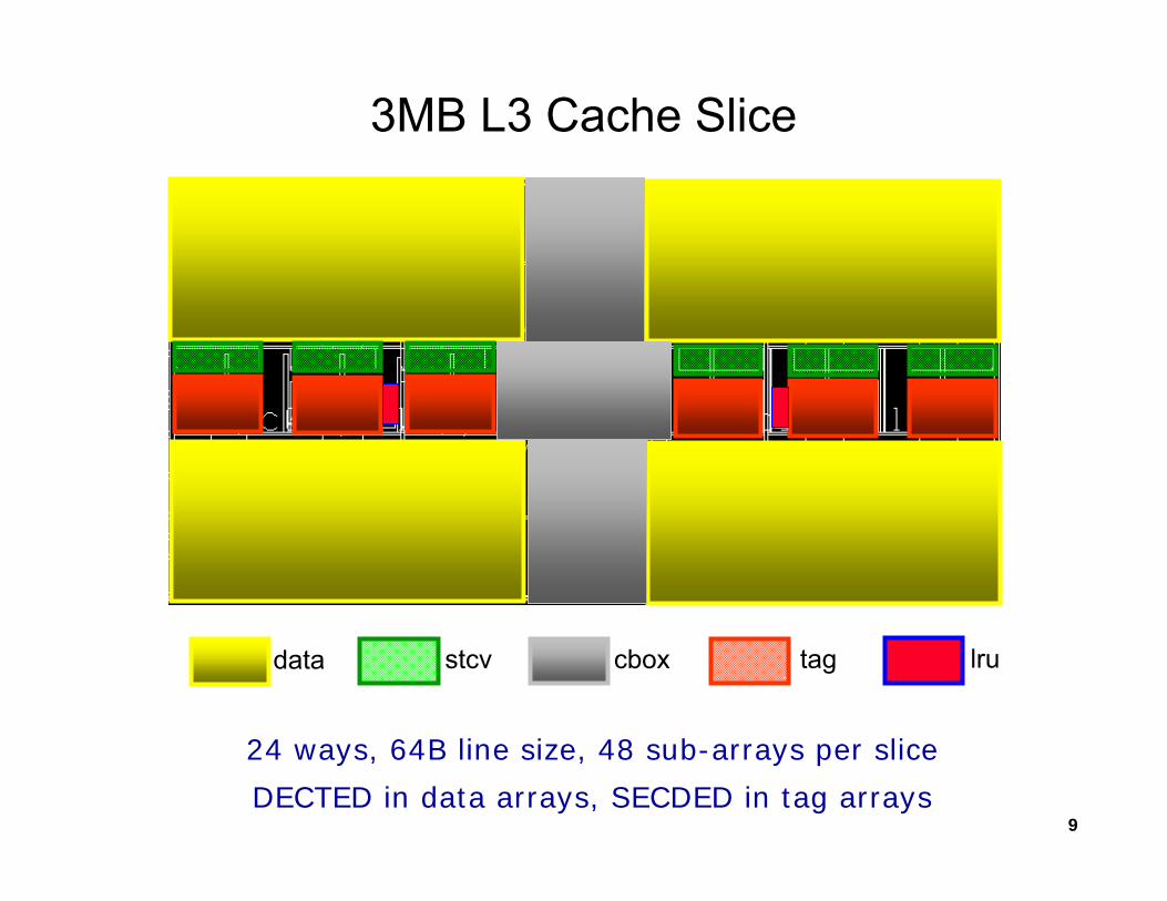
3MB L3 Cache Slice
24 ways, 64B line size, 48 sub-arrays per slice
DECTED in data arrays, SECDED in tag arrays
data tagstcv lrucbox

10
Clock Domains
• 3 primary clock domains:– Core– Un-core– I/O
• 16 PLLs & 8 DLLs– Single system clock
input (BCLK)
SMI SMI
QPI QPI QPI QPI
C3
C2
C1
C0
C4
C5
C6
C7
BCLKBCLK
IO IO PLLsPLLs
IO DLLsIO DLLs
IO IO PLLsPLLs
IO DLLsIO DLLs
UnUn-- core PLLcore PLL Core Core PLLsPLLs
Filter PLLFilter PLL
UnUn-- core PLLcore PLL Core Core PLLsPLLs
Filter PLLFilter PLL
Core Domain (MCLK)
Un-Core Domain (UCLK)
I/O Domain (QCLK)

11
PLL Reference Clocks
FtrPLL UPLL
QPLL QPLLQPLL
QPLL
4 QPI ports
Reference Clocks
BCLK
CPLLCPLL
CPLLCPLL
CPLLCPLL
CPLLCPLLQPLL
QPLL
2 SMI ports
Reference clocks are distributed to 15 destinations
12
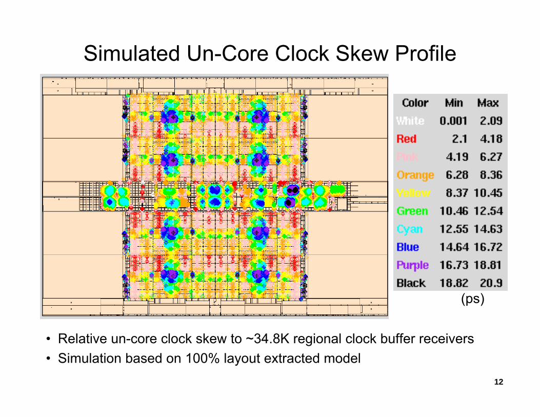
Simulated Un-Core Clock Skew Profile
• Relative un-core clock skew to ~34.8K regional clock buffer receivers• Simulation based on 100% layout extracted model
(ps)

13
Multiple Voltage Domains
Multiple voltage domains minimize power consumption across the core and uncore areas
SMI SMI
QPI QPI QPI QPI
Fuse
CoreSupply
CoreSupply
CoreSupply
CoreSupply
UncoreSupply
Core Domain 0.85-1.1V variable
Un-Core Domain0.9-1.1V
fixed
I/O Domain 1.1Vfixed
14
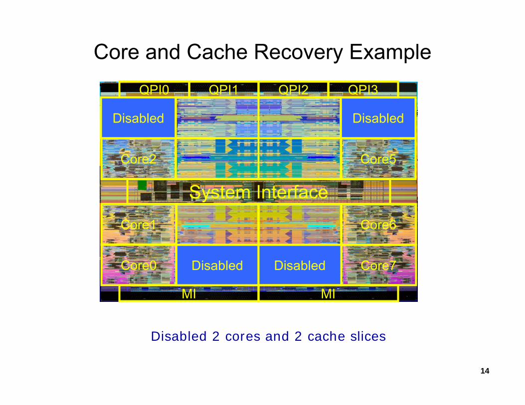
Core and Cache Recovery Example
Disabled 2 cores and 2 cache slices
QPI0 QPI1
Disabled
Core5
Core6
Core7
MI
Disabled
Core2
Core1
Disabled Disabled
System Interface
MI
QPI2 QPI3
Core0

15
Minimize Power in Disabled Blocks
• Disabled cores ► Power gated
• Disabled cache slices ► All major arrays in shut-off
0V
0.9V
Vol
tage
Active Sleep Shut-offVirtual VCC
35% Leakage
Reduction
Active
SRAM array
Sleep/Shut-off
Core
Active/Shut-off
83%
0V
0.85V
Vol
tage
Active Shut-offVirtual VCC
40x Leakage
Reduction

16
Core and Cache Recovery – Infrared Image
All cores and cache slices are enabled

17
Core and Cache Recovery – Infrared Image
Shut-off 2 cores (top row) and 2 cache slices (bottom row)
Disabled blocks are clock and power gated

18
Power and Leakage Breakdown
Power Breakdown Leakage Breakdown
Vcore54.6% Vuncore
33.4%
Vio11.2%
Vpll0.8%
Active84%
Leakage16%
Clock gatingRun uncore at 0.9V
Long channel device usage:58% cores, 85% uncore
Reductiontechniques

19
PackageDetails
• 14 layer organic substrate– 49.1 x 56.4 mm– 5-4-5 layer stacking
• Integrated heat spreader– 35.5 x 43.1 mm
• System management components– ROM’s for processor information
• 1567 total lands at 1.016 mm pitch – 717 signal IO’s
• 32 x 24 mm cavity– Decoupling capacitors on package
bottom directly opposite circuits• 100% lead-free1 and halogen-free2
1 45nm product is manufactured on a lead-free process. Lead is below 1000 PPM per EU RoHS directive (2002/95/EC, Annex A). Some EU RoHS exemptions for lead may apply to other components used in the product package.
2 Applies only to halogenated flame retardants and PVC in components. Halogens are below 900 PPM bromine and 900 PPM chlorine.
20
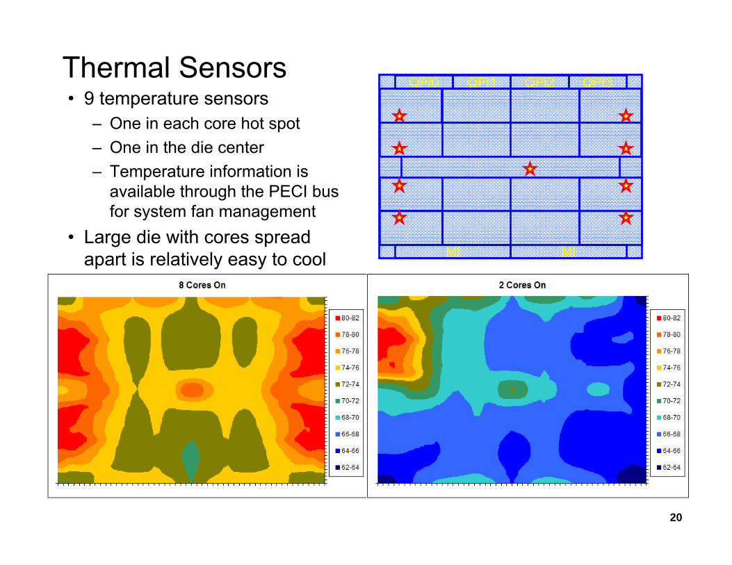
Thermal Sensors• 9 temperature sensors
– One in each core hot spot– One in the die center– Temperature information is
available through the PECI bus for system fan management
• Large die with cores spread apart is relatively easy to cool– Temperatures below 85C
despite over 10C of pre-heat through DRAMs
QPI0 QPI1
MI MI
QPI2 QPI3

21
TX Block Diagram
TX Equalizer & FIFO Block TX Lane
Driver
LinkDetect
1
0
Bias generator
from BGR
Data bits
RTRT
0
1
0
1
FIFO
FIFO
pclk
Tx Eq Coefficients
4 tapTx Eq FIR filter
4 tapTx Eq FIR filter
Direct access
Read pointer
Write pointer
txpclk
Per-lane TX swingcompensation
Global Rtermcompensation

22
RX Block Diagram
3 samplers & VOCs
Rx Controlclk
Rx Lane
Data bits
Offset TrimControl
Rx FIFO
DLL
[3] per bit
0o 45o 90o 135o
VOCCTLE
SampleandHold
PhaseInterpolator
Retiming
Filter &,PI control
FSM
180o 225o 270o 315o
CLK
90
CLK
270
Per-laneRX Irefcompensation
1st orderCTLE
GlobalRtermcompensation
23
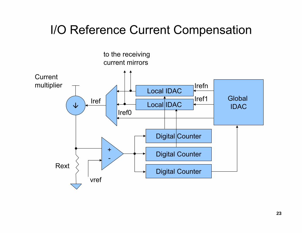
I/O Reference Current Compensation
Global IDAC
+-
vref
Digital Counter
Digital Counter
Local IDAC
Local IDACIref
Rext
Irefn
Iref0
Iref1
Digital Counter
Currentmultiplier
to the receivingcurrent mirrors

24
QPI Eye Diagram
Eye diagram captured on 14”, 1-connector QPI link at 6.4GT/s

25
Disable Unused QPI ports
CPU2CPU2CPU2CPU 1CPU 1CPU 1
IO HUBIO HUB
IO HUBIO HUB
IO HUBIO HUB
CPU 3CPU 3CPU 1CPU 1
CPU 2CPU 2 CPU 4CPU 4
Dual processorwith one IOH
UnusedQPI links
UnpopulatedSocket
Partially populated4 socket board
Legend:

26
Link Detect Circuit
+-VCC/2
RxTerm
Rx Term pulls Tx pad low
Link Detect = 1
VSS VCC
+-VCC/2
No RxTerm
PresentTx pullspad high
Link Detect = 0
VSS VCC
• Link detector senses unused links at power-on and disables them to save ~2W per port– Shut-off all driver bias currents– Turn-off the PLL to stop the clock

27
Load Adaptive Voltage Regulation
Full Load Mode• All VR phases are enabled• Maximum VR efficiency
Idle Mode• Turn off 3 core and 1 cache phases• Maximum VR efficiency
Core VR4 phases Cache VR
3 phases
Nehalem-EXProcessor
PSI_Core PSI_Cache
Nehalem-EX extends the VR phase shut-off to the cache supply
About 2W power reduction per socket in idle mode
Core VR1 phase Cache VR
2 phases
Nehalem-EXProcessor
PSI_Core PSI_Cache

28
Load Efficiency of 4-phase Voltage Regulator
50
55
60
65
70
75
80
85
90
0 5 10 15 20 25 30
Output current (A)
Effi
cien
cy (%
)
1-phase
2-phase
4-phase
Optimal efficiency
Shut-off VR phases in idle mode to improve efficiency
29
Summary• Enterprise-class 45nm 8-cores, 16-threads Xeon®
Processor with 24MB on-die shared L3 cache– Largest transistor count for a microprocessor– Two integrated memory controllers– Four point-to-point links at 6.4GT/s with per-lane compensation
• Active power and leakage reduction techniques– 45nm High-K Metal Gate process reduces leakage– Multiple voltage and clock domains minimize power consumption – Operate at the lowest possible voltage– Extensive use of long channel devices– Automatically disable unused QPI ports at power-on– Load adaptive voltage regulation reduces idle power
• Core and cache recovery enables multiple product options– Disabled cores and cache slices are clock and power gated