near-memory processing - michigan · near-memory processing salessawi ferede yitbarek todd austin...
TRANSCRIPT
11/9/2015
1
NEAR-MEMORY PROCESSING
Salessawi Ferede YitbarekTodd Austin
Outline
Processing-in-Memory Research in the 90’s
2.5D and 3D Integration
Near-Memory Processing
11/9/2015
2
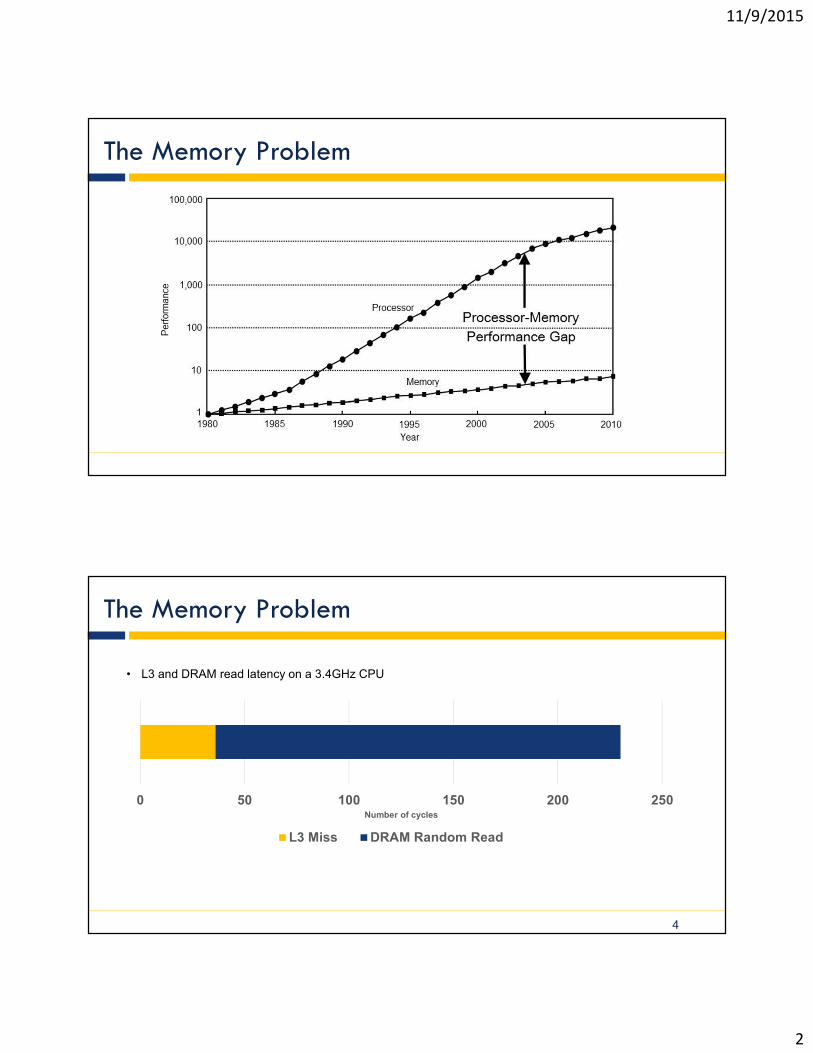
The Memory Problem
The Memory Problem
0 50 100 150 200 250Number of cycles
L3 Miss DRAM Random Read
4
• L3 and DRAM read latency on a 3.4GHz CPU
11/9/2015
3
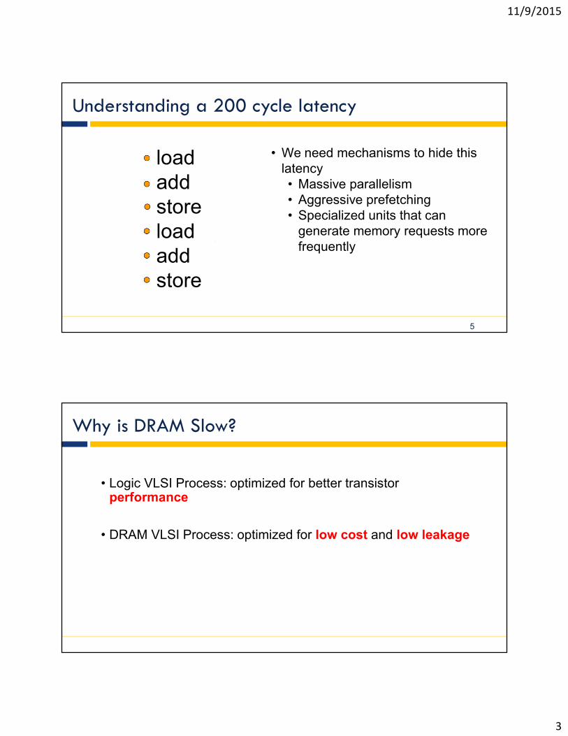
Understanding a 200 cycle latency
5
loadaddstoreloadaddstore
• We need mechanisms to hide this latency• Massive parallelism• Aggressive prefetching• Specialized units that can
generate memory requests more frequently
Why is DRAM Slow?
• Logic VLSI Process: optimized for better transistor performance
• DRAM VLSI Process: optimized for low cost and low leakage

11/9/2015
4
A Highlight of Research from the 90s
Processing-in-Memory7
Processing-in-Memory
Placing processing units on same die with DRAM provides increased bandwidth
Merged Logic and DRAM (MLD) process was emerging IBM, Mitsubishi, Samsung, Toshiba and others
Multiple efforts from industry and academia Micron: Active Memory(Yukon)
UC Berkeley: IRAM
Notre Dame: Execube
MIT: Raw
Stanford: Smart Memories
UIUC: FlexRAM
UC Davis: Active Pages
USC: DIVA
And many more….
11/9/2015
5
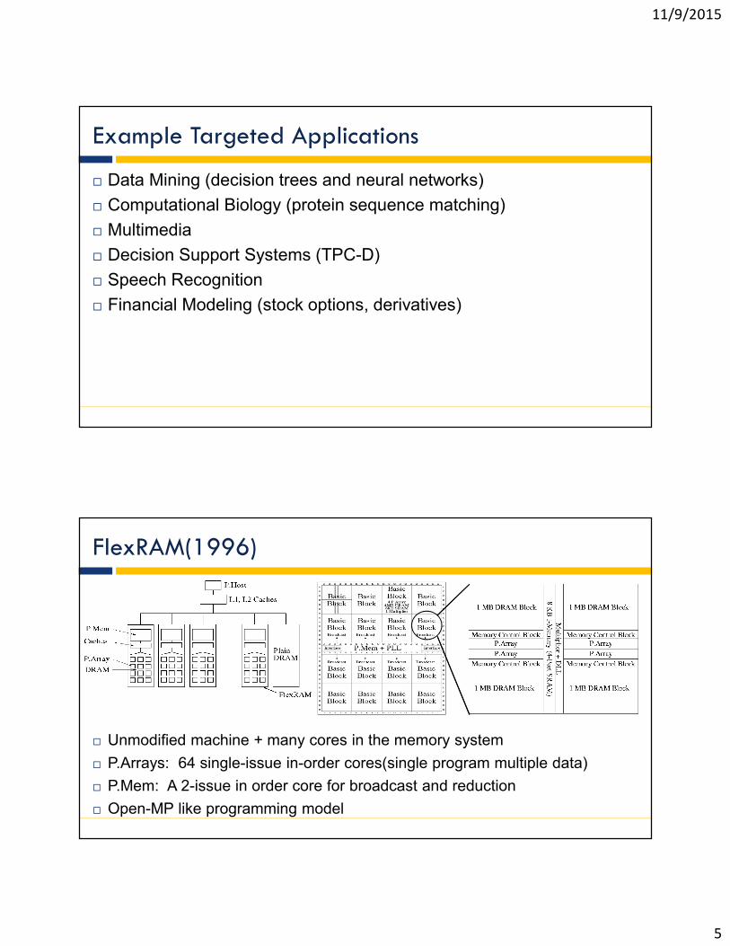
Example Targeted Applications
Data Mining (decision trees and neural networks)
Computational Biology (protein sequence matching)
Multimedia
Decision Support Systems (TPC-D)
Speech Recognition
Financial Modeling (stock options, derivatives)
FlexRAM(1996)
Unmodified machine + many cores in the memory system
P.Arrays: 64 single-issue in-order cores(single program multiple data)
P.Mem: A 2-issue in order core for broadcast and reduction
Open-MP like programming model

11/9/2015
6
Mitsubishi M32Rx/D (HotChips’98)
eRAMTechnology
High bandwidth bus
VIRAM1: Media Oriented Vector PIM(2000-2002)
11/9/2015
7
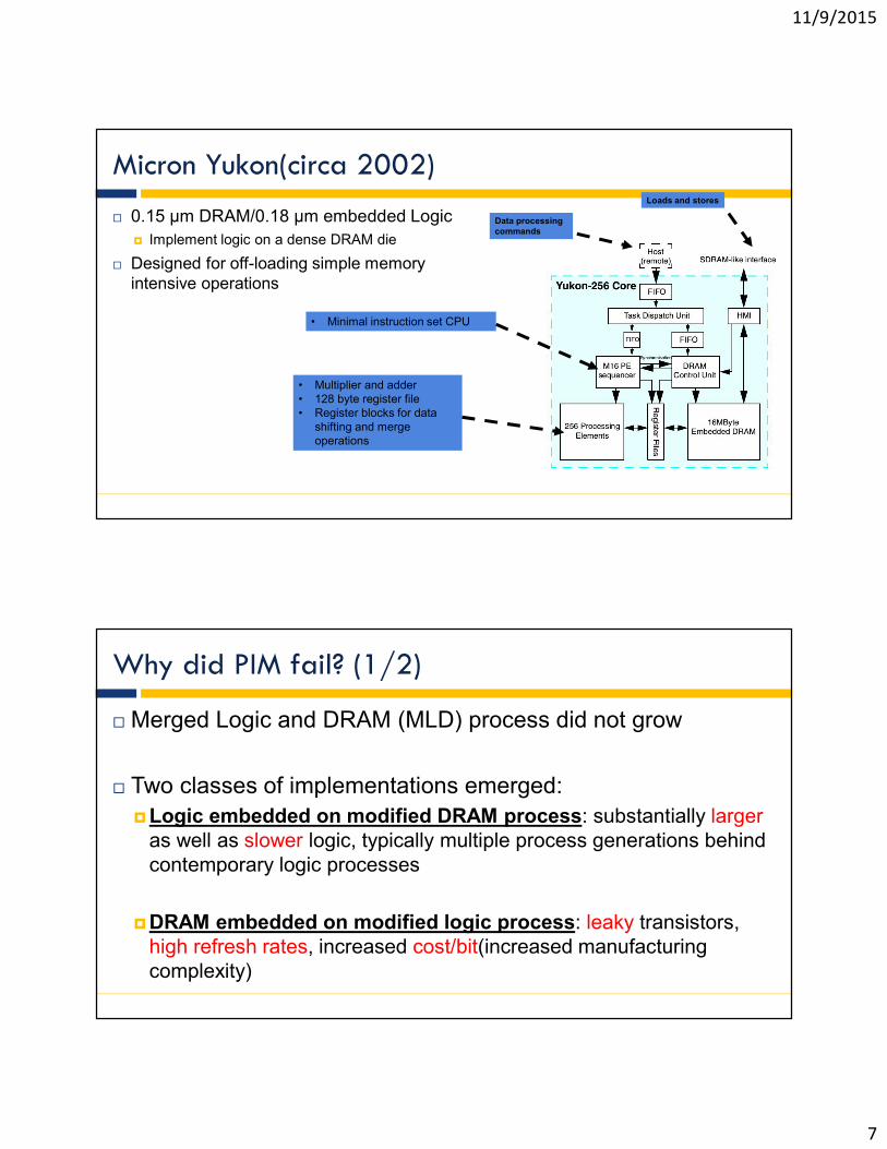
Micron Yukon(circa 2002)
0.15 µm DRAM/0.18 µm embedded Logic
Implement logic on a dense DRAM die
Designed for off-loading simple memory intensive operations
• Multiplier and adder• 128 byte register file• Register blocks for data
shifting and merge operations
• Minimal instruction set CPU
Data processingcommands
Loads and stores
Why did PIM fail? (1/2)
Merged Logic and DRAM (MLD) process did not grow
Two classes of implementations emerged:
Logic embedded on modified DRAM process: substantially largeras well as slower logic, typically multiple process generations behind contemporary logic processes
DRAM embedded on modified logic process: leaky transistors, high refresh rates, increased cost/bit(increased manufacturing complexity)
11/9/2015
8
Why did PIM fail? (2/2)
Reduced performance of logic application specific architectures
Hard to program
No standard interface
Economies of building specialized PIM systems were unattractive to industry
Higher memory cost/bit
Potentially reduced yield
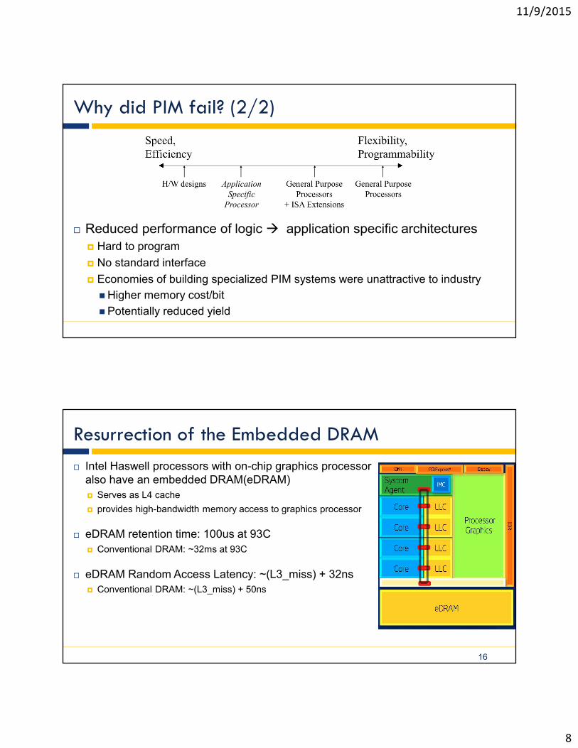
Resurrection of the Embedded DRAM
Intel Haswell processors with on-chip graphics processor also have an embedded DRAM(eDRAM)
Serves as L4 cache
provides high-bandwidth memory access to graphics processor
eDRAM retention time: 100us at 93C
Conventional DRAM: ~32ms at 93C
eDRAM Random Access Latency: ~(L3_miss) + 32ns
Conventional DRAM: ~(L3_miss) + 50ns
16
11/9/2015
9
2.5D and 3D Integration
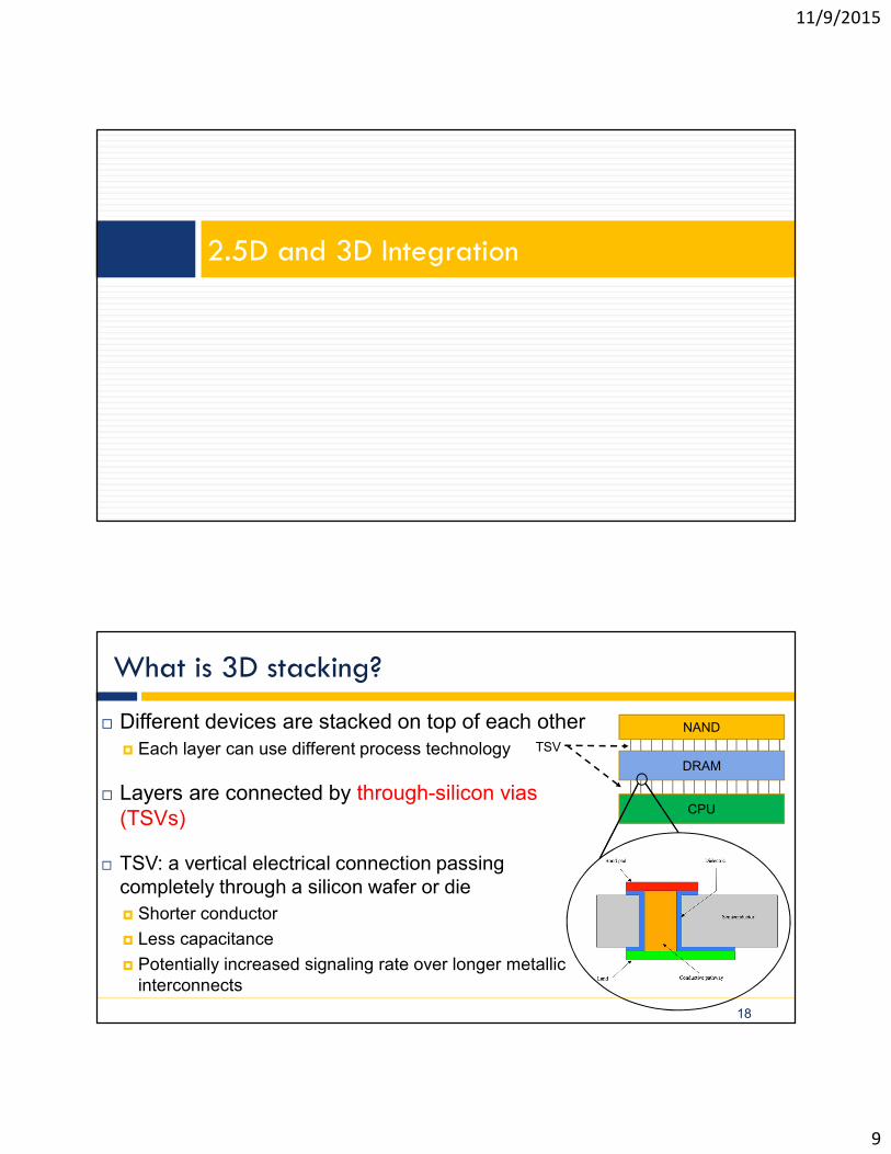
What is 3D stacking?
Different devices are stacked on top of each other Each layer can use different process technology
Layers are connected by through-silicon vias(TSVs)
TSV: a vertical electrical connection passing completely through a silicon wafer or die
Shorter conductor
Less capacitance
Potentially increased signaling rate over longer metallic interconnects
18
NAND
DRAM
CPU
TSV

11/9/2015
10
Why 3D Integration?
Communication between devices bottlenecked by limited I/O pins
Bit-rate supported by long wires is limited
Memory wall: we want to have better DRAM organizations(more on this later…)
Integrating heterogeneous elements on a single wafer is expensive and suboptimal
3D Stacking - Key Challenges
Removing heat from inner layers is challenging
Thermal stress due to TSVs
DRAM requires doubling the refresh rate for temperatures above 85C
Supplying power to all layers
20
NAND
DRAM
CPU
11/9/2015
11
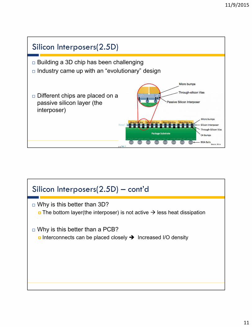
Silicon Interposers(2.5D)
Building a 3D chip has been challenging
Industry came up with an “evolutionary” design
Different chips are placed on a passive silicon layer (the interposer)
Silicon Interposers(2.5D) – cont’d
Why is this better than 3D?
The bottom layer(the interposer) is not active less heat dissipation
Why is this better than a PCB?
Interconnects can be placed closely Increased I/O density
11/9/2015
12
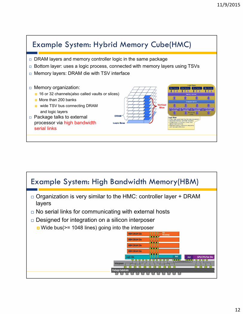
DRAM layers and memory controller logic in the same package
Bottom layer: uses a logic process, connected with memory layers using TSVs
Memory layers: DRAM die with TSV interface
Memory organization:
16 or 32 channels(also called vaults or slices)
More than 200 banks
wide TSV bus connecting DRAM
and logic layers
Package talks to external processor via high bandwidthserial links
Example System: Hybrid Memory Cube(HMC)
Organization is very similar to the HMC: controller layer + DRAM layers
No serial links for communicating with external hosts
Designed for integration on a silicon interposer
Wide bus(>= 1048 lines) going into the interposer
Example System: High Bandwidth Memory(HBM)
11/9/2015
13
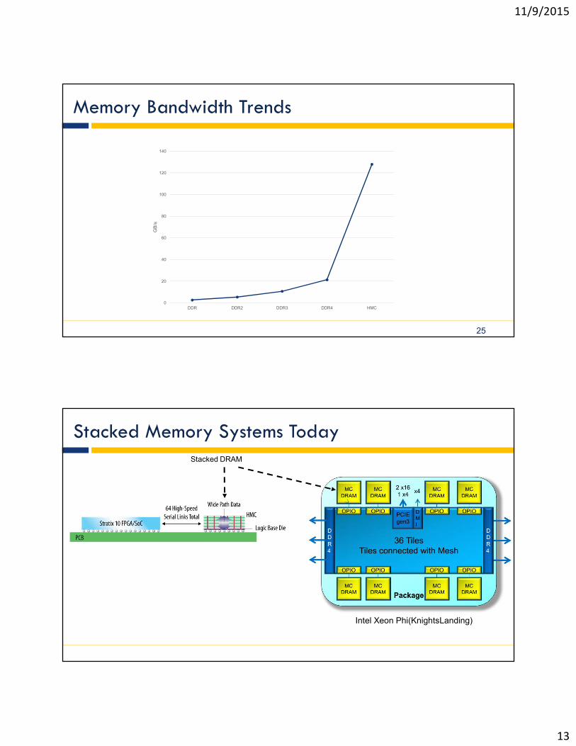
Memory Bandwidth Trends
25
0
20
40
60
80
100
120
140
DDR DDR2 DDR3 DDR4 HMC
GB
/s
Stacked Memory Systems TodayStacked DRAM
Intel Xeon Phi(KnightsLanding)
11/9/2015
14
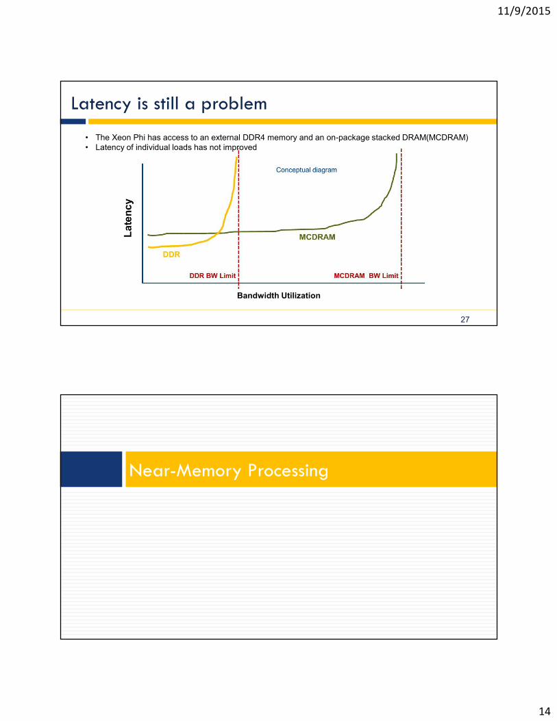
Latency is still a problem
27
Bandwidth Utilization
• The Xeon Phi has access to an external DDR4 memory and an on-package stacked DRAM(MCDRAM)• Latency of individual loads has not improved
Near-Memory Processing

11/9/2015
15
Stacking processors and memory
A fundamental problems with older PIM technologies: slow logic coupled with dense DRAM(or vice versa)
3D stacking solves this problem: different layers can use different process technology
TSVs provide logic layer with high bandwidth access to DRAM banks
Near Memory Processing: Other Enabling Trends
Prevalence of througput-oriented applications
Rise of big-data applications Working sets don’t fit in cache anymore
Matured data parallel and heterogeneous platform programming models CUDA, OpenCL
MapReduce, Spark
Increasing interest in specialized processing units

11/9/2015
16
Example: MapReduce on 3D-Stacked Memory+Logic Devices Workloads[Pugsley et.al.]
16 single-issue in-order cores placed in the bottom layer of the 3D stack
Vertical slices treated as independent silos
Targets massively parallel MapReduce applications
Map phases offloaded to the near memory cores
Terasect: Near-Memory Processing for Parallel Graph Processing[Ahnet.al]
Single-issue in-order cores, coupled with prefetchers optimized for graph processing, are placed at the logic die of each vault
Near-Memory cores access their local DRAM partition only
Low-cost message passing mechanism between near-memory cores
NMC capable memory is separate non-cachable memory (not coherent with the main memory)
11/9/2015
17
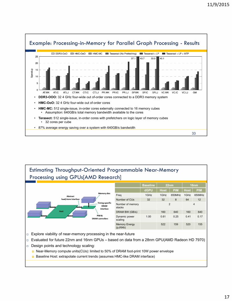
Example: Processing-in-Memory for Parallel Graph Processing - Results
33
• DDR3-OOO: 32 4 GHz four-wide out of-order cores connected to a DDR3 memory system
• HMC-OoO: 32 4 GHz four-wide out of-order cores
• HMC-MC: 512 single-issue, in-order cores externally connected to 16 memory cubes• Assumption: 640GB/s total memory bandwidth available to the cores
• Terasect: 512 single-issue, in-order cores with prefetchers on logic layer of memory cubes• 32 cores per cube
• 87% average energy saving over a system with 640GB/s bandwidth
Estimating Throughput-Oriented Programmable Near-Memory Processing using GPUs[AMD Research]
Explore viability of near-memory processing in the near-future
Evaluated for future 22nm and 16nm GPUs – based on data from a 28nm GPU(AMD Radeon HD 7970)
Design points and technology scaling:
Near-Memory compute units(CUs): limited to 50% of DRAM foot-print 10W power envelope
Baseline Host: extrapolate current trends (assumes HMC-like DRAM interface)
Baseline 22nm 16nm
dGPU Host PIM Host PIM
Freq 1GHz 1GHz 650MHz 1GHz 650MHz
Number of CUs 32 32 8 64 12
Number of memory stacks
2 4
DRAM BW (GB/s) 160 640 160 640
Dynamic power scaling
1.00 0.61 0.25 0.41 0.17
Memory Energy (pJ/64b)
522 159 520 155
11/9/2015
18
0
0.2
0.4
0.6
0.8
1
1.2
1.4
1.6
1.8
2
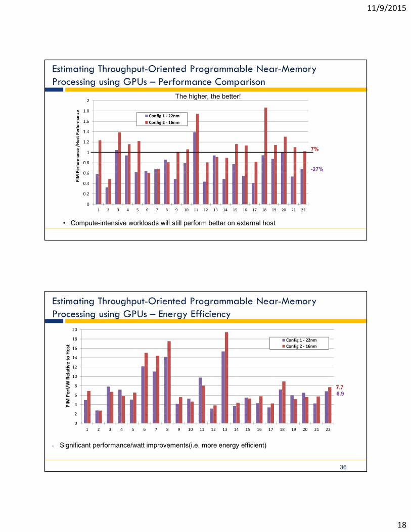
1 2 3 4 5 6 7 8 9 10 11 12 13 14 15 16 17 18 19 20 21 22
PIM
Pe
rfo
rman
ce /
Ho
st P
erf
orm
ance
Config 1 - 22nm
Config 2 - 16nm
The higher, the better!
-27%
7%
• Compute-intensive workloads will still perform better on external host
Estimating Throughput-Oriented Programmable Near-Memory Processing using GPUs – Performance Comparison
Estimating Throughput-Oriented Programmable Near-Memory Processing using GPUs – Energy Efficiency
36
0
2
4
6
8
10
12
14
16
18
20
1 2 3 4 5 6 7 8 9 10 11 12 13 14 15 16 17 18 19 20 21 22
PIM
Pe
rf/W
Re
lati
ve t
o H
ost
Config 1 - 22nm
Config 2 - 16nm
• Significant performance/watt improvements(i.e. more energy efficient)
6.97.7
11/9/2015
19
Challenges
NMC Challenges
Heat
TSV
Thermal stress
Speed vs (yield and size)
Coupling
Power delivery
Coherence
Programming models

11/9/2015
20
3939