near-field imaging of phased array metasurfaces · near-field imaging of phased array metasurfaces...
TRANSCRIPT
Near-Field Imaging of Phased Array MetasurfacesBernhard J. Bohn,†,‡ Martin Schnell,§ Mikhail A. Kats,*,†,∥ Francesco Aieta,† Rainer Hillenbrand,#,⊥
and Federico Capasso†
†School of Engineering and Applied Sciences, Harvard University, Cambridge, Massachusetts 02138, United States‡Fakultat fur Physik, Ludwig-Maximilians-Universitat, 80799 Munchen, Germany§CIC nanoGUNE, 20018 Donostia, San Sebastian, Basque Country, Spain∥Department of Electrical and Computer Engineering, University of Wisconsin −Madison, Madison, Wisconsin 53706, United States#CIC nanoGUNE and EHU/UPV, 20018 Donostia, San Sebastian, Basque Country, Spain⊥IKERBASQUE, Basque Foundation for Science, 48011 Bilbao, Basque Country, Spain
*S Supporting Information
ABSTRACT: Phased-antenna metasurfaces can impart abrupt, spatially dependentchanges to the amplitude, phase, and polarization of light and thus mold wavefrontsin a desired fashion. Here we present an experimental and computational near-fieldstudy of metasurfaces based on near-resonant V-shaped antennas and connect theirnear- and far-field optical responses. We show that far fields can be obtained fromlimited, experimentally obtained knowledge of the near fields, paving the way forexperimental near-field characterization of metasurfaces and other opticalnanostructures and prediction of their far fields from the near-field measurements.
KEYWORDS: Optical antennas, metasurfaces, SNOM, near field, plasmonics
Various widely used optical components such as lenses,prisms, and wave plates rely on the gradual change of
phase and polarization of the light as it propagates throughsome material.1 As nanofabrication technologies have made iteasier to generate structures with length scales smaller than thewavelength of light, new approaches to controlling opticalwavefronts have emerged. One such approach involvesmetasurfaces, which consist of a metallic and/or dielectricpatterned layer (or several layers) with thicknesses muchsmaller than the wavelength of light. The term “flat optics” issometimes used to describe these quasi-two-dimensionalstructures.1,2 Metasurfaces with spatially varying opticalresponse have enabled the observation of new opticalphenomena such as anomalous reflection and refraction3 anddirect coupling to surface waves,4 as well as the development ofultrathin optical components such as planar lenses,5−7 spiralphase plates,8 and wave plates.9
A widely studied metasurface comprises metallic V-shapedantennas which support symmetric and antisymmetric chargeoscillation eigenmodes that can be selectively excited by thetwo linear polarizations of light (Figure 1a). By combining thescattering properties of these two modes, a single V-antennacan be designed to impart a phase shift between the incidentand scattered light in the range from 0 to 2π.3,10 As a resultthese antennas can be tiled to create a metasurface whichmodulates the wavefront of light in a desired fashion. Thesemetasurfaces are often used in cross-polarization mode (e.g., ref3), but other modes of operation are possible.1,9
Since the introduction of these structures, there have beennumerous studies which use metasurfaces for far-field control
(e.g., refs 1−12) but little work to explore their near-fieldproperties. Here we characterized the near-field response ofindividual, isolated V-antennas around resonance using phase-resolved scattering-type scanning near-field optical microscopy(s-SNOM) and compared the experimental results withnumerical simulations. We then examined the near field of anantenna array which imparts a linear phase gradient onto theincident light, resulting in anomalous reflection and refractionin the far field.3 We thus established a connection between thenear- and far-field behavior of metasurfaces.As viewed from the top, our V-antennas consist of two gold
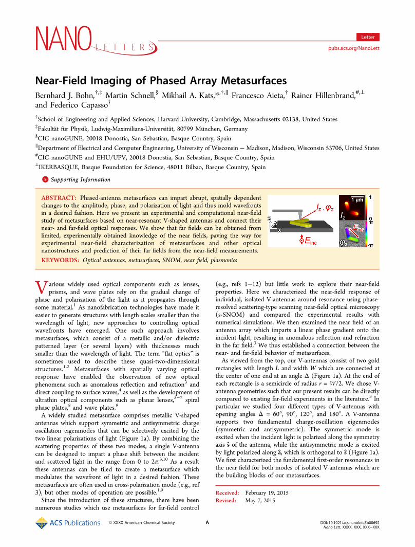
rectangles with length L and width W which are connected atthe center of one end at an angle Δ (Figure 1a). At the end ofeach rectangle is a semicircle of radius r = W/2. We chose V-antenna geometries such that our present results can be directlycompared to existing far-field experiments in the literature.3 Inparticular we studied four different types of V-antennas withopening angles Δ = 60°, 90°, 120°, and 180°. A V-antennasupports two fundamental charge-oscillation eigenmodes(symmetric and antisymmetric). The symmetric mode isexcited when the incident light is polarized along the symmetryaxis s of the antenna, while the antisymmetric mode is excitedby light polarized along a, which is orthogonal to s (Figure 1a).We first characterized the fundamental first-order resonances inthe near field for both modes of isolated V-antennas which arethe building blocks of our metasurfaces.
Received: February 19, 2015Revised: May 7, 2015
Letter
pubs.acs.org/NanoLett
© XXXX American Chemical Society A DOI: 10.1021/acs.nanolett.5b00692Nano Lett. XXXX, XXX, XXX−XXX
The conventional way to probe an antenna resonance is tolook at the response of some quantity (e.g., near-field intensity)for a single antenna as a function of wavelength.13 Because ofexperimental limitations, we instead pursued a complementaryapproach where the wavelength is fixed (λ = 9.3 μm),measuring a series of isolated antennas of varying sizes.14−17
This is roughly equivalent to measuring the wavelength-dependent spectrum of a single antenna due to the scaleinvariance of Maxwell’s equations and the fact that at mid-infrared wavelengths gold behaves similarly to a perfect electricconductor,18 and thus its dispersion can be ignored. We scaledthe length L and width W, maintaining the thickness constantsince it does not change the resonance frequency significantly(see Supporting Information, Section 4). Eleven antenna sizeswere chosen for each opening angle Δ, and the arm length L
and width W increase in equidistant steps from the smallest tothe biggest antenna, such that the ratio L/W is kept constant.The range of sizes was chosen such that the resonances for bothmodes are observed in the experiment.Using electron beam lithography with lift-off, the 50 nm thick
V-antennas were fabricated with gold (Au) on top of a silicon(Si) substrate with a 5 nm titanium (Ti) adhesion layer inbetween (Figure 1b). We utilized s-SNOM in transmissionmode,19−21 which provides amplitude- and phase-resolved near-field mapping. By combining experimental s-SNOM measure-ments with finite-difference time-domain (FDTD) simulationsof the antennas, we gained access to detailed information aboutthe charge distribution at, around, and away from resonance.For this study we considered the intensity Iz = |Ez|
2 and thephase φz = arg(Ez) of the vertical near-field component Ez (see
Figure 1. (a) Schematic of the V-antennas studied in this work. Each antenna is defined by its opening angle Δ, arm length L, and width W. Thesymmetric charge-oscillation eigenmode is excited by light polarized along the symmetry axis of the V-antenna s, and the antisymmetric mode by theorthogonal polarization (along a). The thick arrows with a color gradient indicate the direction of the current flow in each eigenmode while darkercolors represent higher average charge density. The 180° (linear) antenna features only one fundamental eigenmode. (b) Schematic of s-SNOMantenna mapping. The antennas are illuminated from the substrate side at normal incidence with a y-polarized CO2 laser beam (λ = 9.3 μm). Thesymmetric (top sketch, blue) and antisymmetric antenna modes (bottom sketch, red) are excited by aligning the antennas such that s and a areparallel to the polarization of the incident light, respectively. A dielectric tip locally scatters the antenna’s near field. Interferometric detection of thescattered light yields the vertical near-field component Ez and enables calculation of the near-field intensity Iz = |Ez|
2 and the near-field phase φz =arg(Ez) (see Methods section for more details). A full diagram of our s-SNOM setup can be found in ref 35.
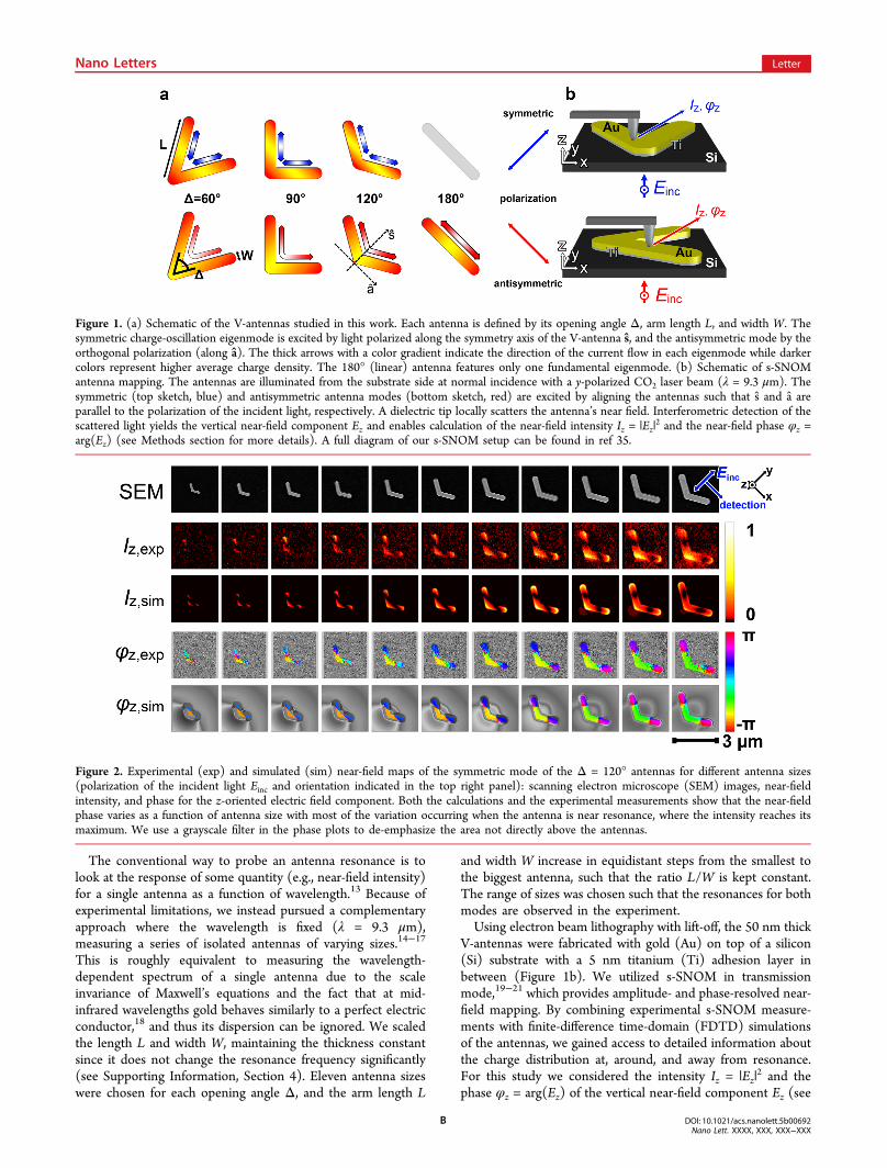
Figure 2. Experimental (exp) and simulated (sim) near-field maps of the symmetric mode of the Δ = 120° antennas for different antenna sizes(polarization of the incident light Einc and orientation indicated in the top right panel): scanning electron microscope (SEM) images, near-fieldintensity, and phase for the z-oriented electric field component. Both the calculations and the experimental measurements show that the near-fieldphase varies as a function of antenna size with most of the variation occurring when the antenna is near resonance, where the intensity reaches itsmaximum. We use a grayscale filter in the phase plots to de-emphasize the area not directly above the antennas.
Nano Letters Letter
DOI: 10.1021/acs.nanolett.5b00692Nano Lett. XXXX, XXX, XXX−XXX
B
Methods section for details). Due to space limitations, we onlypresent the symmetric and antisymmetric modes of the Δ =120° antennas in the main text; the results for all other values ofΔ can be found in the Supporting Information (Section 1).Figure 2 shows the experimental and simulated intensity and
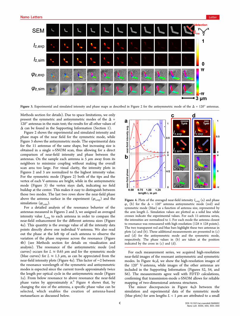
phase maps of the near field for the symmetric mode, whileFigure 3 shows the antisymmetric mode. The experimental datafor the 11 antennas of the same shape, but increasing size isobtained in a single s-SNOM scan, thus allowing for a directcomparison of near-field intensity and phase between theantennas. On the sample each antenna is 5 μm away from itsneighbors to minimize coupling without making the overallscan area too large. For visual clarity, the intensity plots inFigures 2 and 3 are normalized to the highest intensity value.For the symmetric mode (Figure 2) both of the tips and thevertex of each V-antenna are bright, while in the antisymmetricmode (Figure 3) the vertex stays dark, indicating no fieldbuildup at the center. This makes it easy to distinguish betweenthose two modes. The last two rows show the near-field phaseabove the antenna surface in the experiment (φz,exp) and thesimulations (φz,sim).For a detailed analysis of the resonance behavior of the
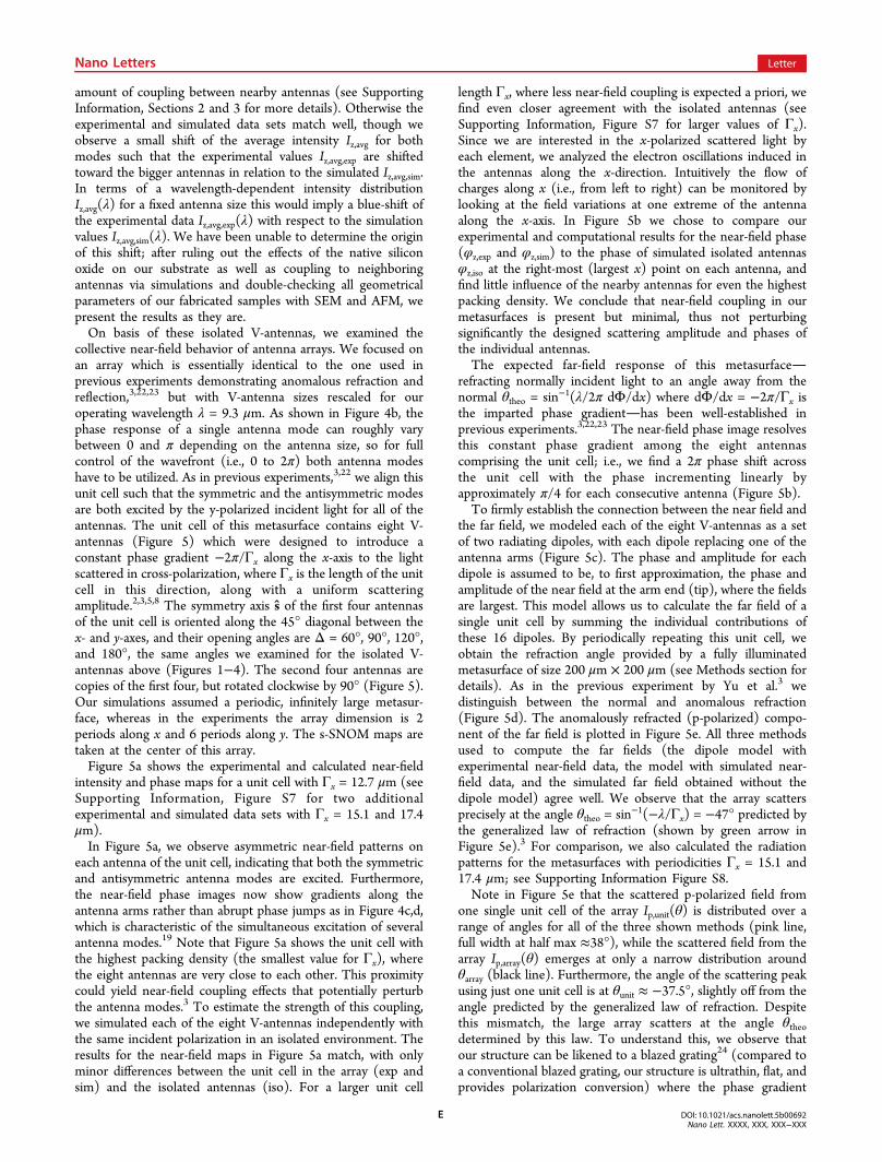
antennas measured in Figures 2 and 3, we assigned an averagedintensity value Iz,avg to each antenna in order to compare thenear-field enhancement for the different antenna sizes (Figure4a). This quantity is the average value of all the intensity datapoints directly above one individual V-antenna. We also readout the phase at the left tip of each antenna to observe thevariation of the phase response across the resonance (Figure4b) (see Methods section for details on visualization andanalysis). The resonance of the antisymmetric mode (redcurves) occurs for L ≈ 0.65 μm and for the symmetric mode(blue curves) for L ≈ 1.3 μm, as can be appreciated from thenear-field intensity plots (Figure 4a). This factor of ∼2 betweenthe resonance wavelength of the symmetric and antisymmetricmodes is expected since the current travels approximately twicethe length per optical cycle in the antisymmetric mode (Figure1a). From below resonance to above resonance the near-fieldphase varies by approximately π.3 Figure 4 shows that, bychanging the size of the antenna, a specific phase value can beselected, which enables the creation of antenna-basedmetasurfaces as discussed below.
For each measurement series, we acquired high-resolutionnear-field images of the resonant antisymmetric and symmetricmodes. In Figure 4c,d, we show the high-resolution images ofthe 120° V-antenna, while images of the other antennas areincluded in the Supporting Information (Figures S2, S4, andS6). The measurements agree well with FDTD calculations,confirming that transmission-mode s-SNOM allows for reliablemapping of two-dimensional antenna structures.The minor discrepancies in Figure 4a,b between the
simulation and experimental data of the symmetric mode(blue plots) for arm lengths L < 1 μm are attributed to a small
Figure 3. Experimental and simulated intensity and phase maps as described in Figure 2 for the antisymmetric mode of the Δ = 120° antennas.
Figure 4. Plots of the averaged near-field intensity Iz,avg (a) and phaseφz (b) for the Δ = 120° antenna antisymmetric mode (red) andsymmetric mode (blue) as a function of antenna size, represented bythe arm length L. Simulation values are plotted as a solid line whilecrosses indicate the experimental values. For each 11-antenna series,the intensities are normalized to 1. For each mode the antenna closestto resonance was remeasured with high resolution (128 × 128 points).The two transparent red and blue bars highlight these two antennas inplots (a) and (b). These additional measurements are presented in (c)and (d) for the antisymmetric mode and the symmetric mode,respectively. The phase values in (b) are taken at the positionindicated by the cross in (c) and (d).
Nano Letters Letter
DOI: 10.1021/acs.nanolett.5b00692Nano Lett. XXXX, XXX, XXX−XXX
C

Figure 5. (a) Experimental (exp) and simulated (sim) near-field maps for the unit cell (Γx = 12.7 μm × Γy = 1.74 μm) of a metasurface antenna arraythat introduces a phase gradient of −2π/Γx to the incident light which is polarized to excite both antenna modes with the same field component:scanning electron microscope (SEM) images, near-field intensity and phase for the z-oriented electric field component. Eight additional simulationswere performed treating each of these V-antennas individually in an isolated environment (iso). (b) Extracted near-field phase at the right-most tip ofthe V-antennas from (a), revealing a near-field phase gradient across the unit cell. Circles mark the experimental near-field phase φz,exp and theposition for each of the eight data points; the solid line shows the data for the simulated near-field phase φz,sim. The crosses in the plot mark the near-field phase values φz,iso above the right-most tip for the respective isolated antennas. (c) Dipole model to represent the unit cell. Each V-antenna isapproximated by two dipoles in the center of both arms. The amplitude and phase values for each dipole are taken in the near-field data of (a) at therespective tip of the V-antenna. (d) Schematic side view of the experiment demonstrating the generalized law of refraction.3 The incident y-polarizedlight hits the metasurface from below at normal incidence. The s-polarized part of the scattered light continues along the surface normal (normalrefraction), whereas the p-polarized part is scattered away from the surface normal at an angle θ (anomalous refraction). (e) Plots of the intensity Ip(p-polarized) in the far field vs θ: We plot the far field for one unit cell (pink) and for a 200 μm × 200 μm array (black) using the dipole model withthe experimental (i) and simulation (ii) near-field data and compare it to the far-field projection from full-wave simulations (iii). The green arrowshows the predicted angle θtheo according to the generalized law of refraction.
Nano Letters Letter
DOI: 10.1021/acs.nanolett.5b00692Nano Lett. XXXX, XXX, XXX−XXX
D
amount of coupling between nearby antennas (see SupportingInformation, Sections 2 and 3 for more details). Otherwise theexperimental and simulated data sets match well, though weobserve a small shift of the average intensity Iz,avg for bothmodes such that the experimental values Iz,avg,exp are shiftedtoward the bigger antennas in relation to the simulated Iz,avg,sim.In terms of a wavelength-dependent intensity distributionIz,avg(λ) for a fixed antenna size this would imply a blue-shift ofthe experimental data Iz,avg,exp(λ) with respect to the simulationvalues Iz,avg,sim(λ). We have been unable to determine the originof this shift; after ruling out the effects of the native siliconoxide on our substrate as well as coupling to neighboringantennas via simulations and double-checking all geometricalparameters of our fabricated samples with SEM and AFM, wepresent the results as they are.On basis of these isolated V-antennas, we examined the
collective near-field behavior of antenna arrays. We focused onan array which is essentially identical to the one used inprevious experiments demonstrating anomalous refraction andreflection,3,22,23 but with V-antenna sizes rescaled for ouroperating wavelength λ = 9.3 μm. As shown in Figure 4b, thephase response of a single antenna mode can roughly varybetween 0 and π depending on the antenna size, so for fullcontrol of the wavefront (i.e., 0 to 2π) both antenna modeshave to be utilized. As in previous experiments,3,22 we align thisunit cell such that the symmetric and the antisymmetric modesare both excited by the y-polarized incident light for all of theantennas. The unit cell of this metasurface contains eight V-antennas (Figure 5) which were designed to introduce aconstant phase gradient −2π/Γx along the x-axis to the lightscattered in cross-polarization, where Γx is the length of the unitcell in this direction, along with a uniform scatteringamplitude.2,3,5,8 The symmetry axis s of the first four antennasof the unit cell is oriented along the 45° diagonal between thex- and y-axes, and their opening angles are Δ = 60°, 90°, 120°,and 180°, the same angles we examined for the isolated V-antennas above (Figures 1−4). The second four antennas arecopies of the first four, but rotated clockwise by 90° (Figure 5).Our simulations assumed a periodic, infinitely large metasur-face, whereas in the experiments the array dimension is 2periods along x and 6 periods along y. The s-SNOM maps aretaken at the center of this array.Figure 5a shows the experimental and calculated near-field
intensity and phase maps for a unit cell with Γx = 12.7 μm (seeSupporting Information, Figure S7 for two additionalexperimental and simulated data sets with Γx = 15.1 and 17.4μm).In Figure 5a, we observe asymmetric near-field patterns on
each antenna of the unit cell, indicating that both the symmetricand antisymmetric antenna modes are excited. Furthermore,the near-field phase images now show gradients along theantenna arms rather than abrupt phase jumps as in Figure 4c,d,which is characteristic of the simultaneous excitation of severalantenna modes.19 Note that Figure 5a shows the unit cell withthe highest packing density (the smallest value for Γx), wherethe eight antennas are very close to each other. This proximitycould yield near-field coupling effects that potentially perturbthe antenna modes.3 To estimate the strength of this coupling,we simulated each of the eight V-antennas independently withthe same incident polarization in an isolated environment. Theresults for the near-field maps in Figure 5a match, with onlyminor differences between the unit cell in the array (exp andsim) and the isolated antennas (iso). For a larger unit cell
length Γx, where less near-field coupling is expected a priori, wefind even closer agreement with the isolated antennas (seeSupporting Information, Figure S7 for larger values of Γx).Since we are interested in the x-polarized scattered light byeach element, we analyzed the electron oscillations induced inthe antennas along the x-direction. Intuitively the flow ofcharges along x (i.e., from left to right) can be monitored bylooking at the field variations at one extreme of the antennaalong the x-axis. In Figure 5b we chose to compare ourexperimental and computational results for the near-field phase(φz,exp and φz,sim) to the phase of simulated isolated antennasφz,iso at the right-most (largest x) point on each antenna, andfind little influence of the nearby antennas for even the highestpacking density. We conclude that near-field coupling in ourmetasurfaces is present but minimal, thus not perturbingsignificantly the designed scattering amplitude and phases ofthe individual antennas.The expected far-field response of this metasurface
refracting normally incident light to an angle away from thenormal θtheo = sin−1(λ/2π dΦ/dx) where dΦ/dx = −2π/Γx isthe imparted phase gradienthas been well-established inprevious experiments.3,22,23 The near-field phase image resolvesthis constant phase gradient among the eight antennascomprising the unit cell; i.e., we find a 2π phase shift acrossthe unit cell with the phase incrementing linearly byapproximately π/4 for each consecutive antenna (Figure 5b).To firmly establish the connection between the near field and
the far field, we modeled each of the eight V-antennas as a setof two radiating dipoles, with each dipole replacing one of theantenna arms (Figure 5c). The phase and amplitude for eachdipole is assumed to be, to first approximation, the phase andamplitude of the near field at the arm end (tip), where the fieldsare largest. This model allows us to calculate the far field of asingle unit cell by summing the individual contributions ofthese 16 dipoles. By periodically repeating this unit cell, weobtain the refraction angle provided by a fully illuminatedmetasurface of size 200 μm × 200 μm (see Methods section fordetails). As in the previous experiment by Yu et al.3 wedistinguish between the normal and anomalous refraction(Figure 5d). The anomalously refracted (p-polarized) compo-nent of the far field is plotted in Figure 5e. All three methodsused to compute the far fields (the dipole model withexperimental near-field data, the model with simulated near-field data, and the simulated far field obtained without thedipole model) agree well. We observe that the array scattersprecisely at the angle θtheo = sin−1(−λ/Γx) = −47° predicted bythe generalized law of refraction (shown by green arrow inFigure 5e).3 For comparison, we also calculated the radiationpatterns for the metasurfaces with periodicities Γx = 15.1 and17.4 μm; see Supporting Information Figure S8.Note in Figure 5e that the scattered p-polarized field from
one single unit cell of the array Ip,unit(θ) is distributed over arange of angles for all of the three shown methods (pink line,full width at half max ≈38°), while the scattered field from thearray Ip,array(θ) emerges at only a narrow distribution aroundθarray (black line). Furthermore, the angle of the scattering peakusing just one unit cell is at θunit ≈ −37.5°, slightly off from theangle predicted by the generalized law of refraction. Despitethis mismatch, the large array scatters at the angle θtheodetermined by this law. To understand this, we observe thatour structure can be likened to a blazed grating24 (compared toa conventional blazed grating, our structure is ultrathin, flat, andprovides polarization conversion) where the phase gradient
Nano Letters Letter
DOI: 10.1021/acs.nanolett.5b00692Nano Lett. XXXX, XXX, XXX−XXX
E

imparted by the single unit cell of the array provides the“blaze”. Though θunit is not precisely equal to θarray, the blazeselects a single diffraction order of the array which beams lightat precisely θtheo. For this reason such metasurfaces are robustto small errors in design or fabrication of the individualantennas.The ability to connect near-field and far-field behavior of
antenna arrays is significant not only because it enhances ourunderstanding of metasurfaces, but also because it suggests thatnear-field measurements such as phase-resolved s-SNOM canbe used to predict the corresponding far-field radiation patternsof a wide variety of optical structures. In full-wave electro-magnetic simulations, complete information about near fields iscommonly used to predict far fields via so-called “far-fieldtransformations”,25 which are made possible by the surfaceequivalence principle.26 These transformations require knowl-edge of the full vectorial near field along some surface. Inexperiments, however, the near-field information is almostalways limited; for example, the present s-SNOM experimentonly provides information about the z-component of theelectric field. Despite this limited information, we demonstratedhere that the far-field response can still be predicted. Weexplain this finding by the fact that for thin antenna structuresthe z-component of the complex near field is a good proxy forthe time-varying charge distribution in the antennas and hencetheir far-field scattering properties. While the dipole modelpresented here already yields good prediction of the far field,we envision more sophisticated models where the near field ateach position on the antenna surface is taken into account.Such limited-information far-field transformations are worthexploring further in future studies.We demonstrated near-field imaging of phase gradients in
optical metasurfaces based on plasmonic V-shaped antennas. Byapplying phase-resolved scattering-type scanning near-fieldoptical microscopy (s-SNOM) at infrared wavelengths, wemeasured the oscillating charge distributions in individual V-shaped antennas and in metasurfaces comprising closely packedantennas, obtaining results in close agreement with full-wavesimulations. The near-field images showed that tailoring thesize and geometry of the antennas determines their amplitudeand phase response, confirming the mechanism for achievingoptical phase discontinuities. By combining the SNOMmeasurements with a model based on oscillating dipoles, weconnected the near- and far fields of phased antennametasurfaces, finding that the far-field response can be inferredfrom limited, experimentally obtained knowledge of the nearfields. This study paves the way for experimental near-fieldcharacterization of a large variety of metasurfaces based onmetal antennas and a prediction of their far fields from near-field measurements.Methods. Fabrication. The antennas were fabricated on
high resistivity (>10 000 Ω cm) double side polished siliconusing a conventional electron beam (e-beam) lithographyprocess with lift-off. A double layer of poly(methylmethacrylate) (PMMA) resist (495A4, then 950A2; Micro-Chem) was spun at 4000 rpm onto the silicon wafer, baked at180 °C for 3 min, and then exposed using a 100 kV e-beamsystem (Elionix ELS-F125). After development with 3:1isopropanol−methyl isobutyl ketone (IPA−MIBK), a 5 nmtitanium adhesion layer and 45 nm of gold were depositedusing e-beam evaporation, and the lift-off process wascompleted in acetone with ultrasonic agitation. For SEMimages of the resulting structures, see Figures 2, 3, and 5.
s-SNOM Measurements. Near-field microscopy setup: weapply interferometric scattering-type scanning near-field opticalmicroscopy (s-SNOM)27−34 to map our antenna structures.Our s-SNOM setup is based on an atomic force microscope(AFM), where commercial silicon tips (NanoWorld, Arrow-NRC-50) are used to locally scatter the antenna nearfield.14,35,19,20,29,34 The sample and tip were illuminated frombelow at normal incidence with a weakly focused CO2 laserbeam at λ = 9.3 μm (transmission-mode s-SNOM19,20,35), thusensuring homogeneous illumination of a relatively large area onthe sample (i.e., covering each complete series of antennas inFigures 2-5) without phase-retardation effects. This illumina-tion closely approximated a plane wave, matching theexperimental conditions in the original far-field experiments.3
In all of the presented experiments the illuminating beampropagated in the positive z-direction and its polarization wasfixed along the y-axis. Excitation of the symmetric mode for theisolated V-antennas in Figure 2 was achieved by aligning the V-antennas’ symmetry axis s along the y-direction. Likewise,excitation of the antisymmetric mode in Figure 3 was achievedby aligning the axis a along the y-direction. To avoid samplerotation between the measurements, we fabricated two sets ofV-antennas on the same substrate where the individualantennas of the second set (antisymmetric mode, Figure 3)were rotated by 90° with respect to the antennas of the first set(symmetric mode, Figure 2).Using a parabolic mirror we collected the tip-scattered light
in the x-direction at an angle of 60° from the surface normal.The tip-scattered near field was interfered with a phase-modulated, vertically (z-) polarized reference beam at theinfrared detector and recorded simultaneously with the sampletopography. Background contributions could be fully sup-pressed by vertical tip oscillation at a frequency Ω = 250 kHz(tapping-mode AFM) and by subsequent higher harmonicdemodulation of the detector signal at 3Ω.21 In this case, thevertical polarization of the reference beam selected the p-component of the tip-scattered light, which mainly contains thevertical (z-) component of the antenna near fields.19,20,35 Usingthis pseudoheterodyne detection module (www.neaspec.com)the amplitude |Ez| and phase φz of the vertical near-fieldcomponent Ez were measured for each scanning point. Thenear-field intensity is then easily calculated by Iz = |Ez|
2.Note that it has been found recently that there are different
scattering mechanisms in s-SNOM imaging of metal anten-nas:15,36 (i) direct scattering of the antenna near fields by thetip into the far field (detector) and (ii) scattering of the antennanear fields by the tip via the antenna itself. When imagingresonant linear antennas, excitation with s-polarization anddetecting the s-component of the scattered light is mainly basedon mechanism (ii), while detecting the p-component is mainlybased on mechanism (i), where the latter was found toessentially yield the z-component, Ez, of the near fields on theantenna surface.36 In our case we aligned the V-antennas such(see Figure 1b) that the excited dipole moment radiates with s-polarization in direction of the detection. In this configuration,the p-component of the scattered light is mainly based onmechanism (i) and we essentially detect the vertical (z-)component of the local near fields, which is furthermoresupported by the good agreement of the experimental imageswith the simulations in Figures 2−5.
Simulations. The FDTD simulations were performed using“FDTD Solutions” from Lumerical running on a workstation.For Figures 2 and 3 (also the 55 isolated antennas in the
Nano Letters Letter
DOI: 10.1021/acs.nanolett.5b00692Nano Lett. XXXX, XXX, XXX−XXX
F

Supporting Information, Section 1) and the isolated V-antennasof Figure 5, the simulation of each V-antenna was done inside avolume of 6.2 μm × 6.2 μm × 1.5 μm using a total-fieldscattered-field (TFSF) plane wave source (λ = 9.3 μm) withperfectly matched layer (PML) boundary conditions. Incontrast to the experiment these V-antennas are truly isolatedsince there are no excited antennas nearby, which couldinfluence each other.The simulations for the three antenna arrays (Figure 5a and
Supporting Information, Figure S7) use periodic boundaryconditions to define a single repeating unit cell with eightantennas in it. A plane wave (λ = 9.3 μm) was launched fromthe silicon side to illuminate this antenna array. So, we simulatean infinite array whereas in the experiment we measure in themiddle of an array of limited size. In all of our simulations weneglect the influence of the cantilever with the silicon tip andthe roughness of the gold surface. The relevant monitor(frequency-domain field and power monitor) for the near fieldwas located at a height of 40 nm above the antenna surfacewhere we obtained a good match with the experimental near-field images.19,20 We took the complex refractive indices givenby Palik37 for Ti, Au and Si.Visualization and Analysis of the Near Field. The
visualization and analysis of experimental and simulated datawas performed using Matlab. We used the intensity and phaseof the complex near-field component Ez. For visual comparisonwe plot the intensity Iz = |Ez|
2 and phase φz = arg(Ez) for all ofthe V-antennas (compare to Figures 2 and 3). The colorbar forthe intensity maps in Figures 2, 3, and 5 is stretched to showthe whole series of resonant and nonresonant antennas in onecolorscale; this was not needed in Figure 4 where just one V-antenna is shown and the conventional “hot” colorscale wasused. In order to analyze the near-field response of eachisolated antenna we took two physical quantities for eachantenna. First we calculated one distinct average intensity valueIz,avg for each antenna, which is the sum of all the singleintensity data points above the actual antenna position dividedby a unitless factor referring to the top-surface area of therespective V-antenna. Then, for each V-antenna series of 11antennas the average intensity was normalized to unity (Figure4a). The phase value was measured as the second quantity. Forthe analysis of Figure 4b we defined the phase as the phasevalue of that point of the left V-antenna tip, where the intensityreaches its maximum. These are data points with a strong signaland thus reliable phase values. Then all of the phase values ineach antenna series have been shifted up or down by a constantfactor so that the phase value equals π /2 at the peak of the Iz,avggraph (compare to Figure 4).Calculation of the Far Field. Our model treats each arm of
the V-antenna as a radiating dipole. These two dipoles areoriented parallel to the arms they replace and are located in thecenter of the respective arms. The phase and amplitude for eachdipole are extracted at the arm end (tip). Then for each of theseradiating dipoles p we can calculate the exact electric fieldEdip(r, p) in air at a given position r in the far field.38,39 In thisapproximation we neglect the silicon substrate.40
We found the far field by calculating the electric field on asemicircle in the xz-plane above the metasurface with a radiusof d = 1 m (Figure 5d). For each position on this circle in thefar field the total electric field scattered by one unit cell can becalculated using the superposition principle by summing up thefields created by the 16 dipoles of this unit cell, Eunit(r) =∑i=1
16 Edip(r − ri, pi) where ri is the position of the i-th dipole in
the unit cell. To model a finite-size incident beam, we sum Eunitover of 16 unit cells along x and 115 cells along y, to obtain anarray with the size of about 200 μm × 200 μm. This way usingall of the dipoles we calculate the total electric field scattered bythe metasurface Earray(r) = ∑nx,nyEunit(ru(nx, ny)), with ru beingthe center of the unit cell (nx, ny).
■ ASSOCIATED CONTENT*S Supporting InformationExperimental and simulation data for V-antenna types notshown in the main text. Near-field maps and far-fieldcalculations for metasurfaces with various periods. Comparisonof the average intensity between different series of isolatedantennas and more information on coupling between antennas.Effect of the antenna thickness on the resonance condition. TheSupporting Information is available free of charge on the ACSPublications website at DOI: 10.1021/acs.nanolett.5b00692.
■ AUTHOR INFORMATIONCorresponding Author*E-mail: [email protected] AddressF.A.: Hewlett-Packard Laboratories, Palo Alto, California94304, USA.Author ContributionsB.J.B. and M.S. contributed equally.NotesThe authors declare the following competing financialinterest(s): R.H. is co-founder of Neaspec GmbH, a companyproducing scattering-type scanning near-field optical micro-scope systems. All other authors declare no competing financialinterests..
■ ACKNOWLEDGMENTSThe authors acknowledge helpful discussions with N. Yu, P.Genevet, and Z. Gaburro. F.C. acknowledges financial supportfrom the Air Force Office of Scientific Research under grantnumber FA9550-12-1-0289 and from Draper Laboratory. M.S.and R.H. acknowledge financial support by the ERC StartingGrant No. 258461 (TERATOMO) and by the National ProjectMAT2012-36580 from the Spanish Ministry of Economy andCompetitiveness. The samples were fabricated in the Center forNanoscale Systems at Harvard University, which is a member ofthe National Nanotechnology Infrastructure Network sup-ported by the National Science Foundation.
■ REFERENCES(1) Yu, N.; Genevet, P.; Aieta, F.; Kats, M. A.; Blanchard, R.; Aoust,G.; Tetienne, J.-P.; Gaburro, Z.; Capasso, F. IEEE J. Quantum Electron.2013, 19, 4700423.(2) Yu, N.; Capasso, F. Nat. Mater. 2014, 13, 139−150.(3) Yu, N.; Genevet, P.; Kats, M. A.; Aieta, F.; Tetienne, J.-P.;Capasso, F.; Gaburro, Z. Science 2011, 334, 333−337.(4) Sun, S.; He, Q.; Xiao, S.; Xu, Q.; Li, X.; Zhou, L. Nat. Mater.2012, 11, 426−431.(5) Aieta, F.; Genevet, P.; Kats, M. A.; Yu, N.; Blanchard, R.;Gaburro, Z.; Capasso, F. Nano Lett. 2012, 12, 4932−4936.(6) Ni, X.; Ishii, S.; Kildishev, A. V.; Shalaev, V. M. Light: Sci. Appl.2013, 2, e72.(7) Chen, X.; Huang, L.; Muhlenbernd, H.; Li, G.; Bai, B.; Tan, Q.;Jin, G.; Qiu, C.-W.; Zhang, S.; Zentgraf, T. Nat. Commun. 2012, 3,1198.
Nano Letters Letter
DOI: 10.1021/acs.nanolett.5b00692Nano Lett. XXXX, XXX, XXX−XXX
G

(8) Genevet, P.; Yu, N.; Aieta, F.; Lin, J.; Kats, M. A.; Blanchard, R.;Scully, M. O.; Gaburro, Z.; Capasso, F. Appl. Phys. Lett. 2012, 100,013101.(9) Yu, N.; Aieta, F.; Genevet, P.; Kats, M. A.; Gaburro, Z.; Capasso,F. Nano Lett. 2012, 12, 6328−6333.(10) Kats, M. A.; Genevet, P.; Aoust, G.; Yu, N.; Blanchard, R.; Aieta,F.; Gaburro, Z.; Capasso, F. Proc. Natl. Acad. Sci. U.S.A. 2012, 109,12364−12368.(11) Pfeiffer, C.; Grbic, A. Phys. Rev. Lett. 2013, 110, 197401.(12) Zhao, Y.; Alu, A. Phys. Rev. B: Condens. Matter Mater. Phys.2011, 84, 205428.(13) Kats, M. A.; Yu, N.; Genevet, P.; Gaburro, Z.; Capasso, F. Opt.Express 2011, 19, 21748−21753.(14) Dorfmuller, J.; Vogelgesang, R.; Weitz, R. T.; Rockstuhl, C.;Etrich, C.; Pertsch, T.; Lederer, F.; Kern, K. Nano Lett. 2009, 9, 2372−2377.(15) Alonso-Gonzalez, P.; Albella, P.; Schnell, M.; Chen, J.; Huth, F.;Garcia-Etxarri, A.; Casanova, F.; Golmar, F.; Arzubiaga, L.; Hueso, L.E.; Aizpurua, J.; Hillenbrand, R. Nat. Commun. 2012, 3, 684.(16) Dorfmuller, J.; Vogelgesang, R.; Khunsin, W.; Rockstuhl, C.;Etrich, C.; Kern, K. Nano Lett. 2010, 10, 3596−3603.(17) Alonso-Gonzalez, P.; Albella, P.; Neubrech, F.; Huck, C.; Chen,J.; Golmar, F.; Casanova, F.; Hueso, L. E.; Pucci, A.; Aizpurua, J.;Hillenbrand, R. Phys. Rev. Lett. 2013, 110, 203902.(18) Novotny, L. Phys. Rev. Lett. 2007, 98, 266802.(19) Schnell, M.; Garcia-Etxarri, A.; Huber, A. J.; Crozier, K.;Aizpurua, J.; Hillenbrand, R. Nat. Photonics 2009, 3, 287−291.(20) Schnell, M.; Garcia-Etxarri, A.; Alkorta, J.; Aizpurua, J.;Hillenbrand, R. Nano Lett. 2010, 10, 3524−3528.(21) Ocelic, N.; Huber, A.; Hillenbrand, R. Appl. Phys. Lett. 2006, 89,101124.(22) Aieta, F.; Genevet, P.; Yu, N.; Kats, M. A.; Gaburro, Z.; Capasso,F. Nano Lett. 2012, 12, 1702−1706.(23) Ni, X.; Emani, N. K.; Kildish, A. V.; Boltasseva, A.; Shalaev, V.M. Science 2012, 335, 427−427.(24) Larouche, S.; Smith, D. R. Opt. Lett. 2012, 37, 2391−2393.(25) Barth, M. J.; McLeod, R. R.; Ziolkowski, R. W. J. Electromagn.Waves Appl. 1992, 6, 5−18.(26) Balanis, C. A. Advanced engineering electromagnetics; Wiley: NewYork, 1989.(27) Hillenbrand, R.; Keilmann, F. Appl. Phys. B: Lasers Opt. 2001,73, 239−243.(28) Hillenbrand, R.; Keilmann, F.; Hanarp, P.; Sutherland, D. S.;Aizpurua, J. Appl. Phys. Lett. 2003, 83, 368−370.(29) Esteban, R.; Vogelgesang, R.; Dorfmuller, J.; Dmitriev, A.;Rockstuhl, C.; Etrich, C.; Kern, K. Nano Lett. 2008, 8, 3155−3159.(30) Olmon, R. L.; Krenz, P. M.; Jones, A. C.; Boreman, G. D.;Raschke, M. B. Opt. Express 2008, 16, 20295−20305.(31) Kim, Z. H.; Leone, S. R. Opt. Express 2008, 16, 1733−1741.(32) Kim, D.-S.; Heo, J.; Ahn, S.-H.; Han, S. W.; Yun, W. S.; Kim, Z.H. Nano Lett. 2009, 9, 3619−3625.(33) Kim, D.-S.; Kim, Z. H. J. Korean Phys. Soc. 2008, 52, 17−20.(34) Rang, M.; Jones, A. C.; Zhou, F.; Li, Z.-Y.; Wiley, B. J.; Xia, Y.;Raschke, M. B. Nano Lett. 2008, 8, 3357−3363.(35) Schnell, M.; Garcia-Etxarri, A.; Huber, A. J.; Crozier, K. B.;Borisov, A.; Aizpurua, J.; Hillenbrand, R. J. Phys. Chem. C 2010, 114,7341−7345.(36) Neuman, T. Mapping the near-fields of plasmonic nanoantennasby scattering-type Scanning Near-field Optical Microscopy. Submittedto Laser Photonics Rev.(37) Palik, E. D. Handbook of optical constants of solids; AcademicPress: San Diego, 1998.(38) Jackson, J. D. Classical electrodynamics, Vol. 3; Wiley: New York,1962.(39) Tetienne, J.-P.; Blanchard, R.; Yu, N.; Genevet, P.; Kats, M. A.;Fan, J. A.; Edamura, T.; Furuta, S.; Yamanishi, M.; Capasso, F. New J.Phys. 2011, 13, 053057.
(40) Blanchard, R.; Aoust, G.; Genevet, P.; Yu, N.; Kats, M. A.;Gaburro, Z.; Capasso, F. Phys. Rev. B: Condens. Matter Mater. Phys.2012, 85, 155457.
Nano Letters Letter
DOI: 10.1021/acs.nanolett.5b00692Nano Lett. XXXX, XXX, XXX−XXX
H