nc 1 8nc rfin 2 7rfout bias nc 3 control 6nc … gain block data sheet adl5531 rev. c document...
TRANSCRIPT

20 MHz to 500 MHz IF Gain Block
Data Sheet ADL5531
Rev. C Document Feedback Information furnished by Analog Devices is believed to be accurate and reliable. However, no responsibility is assumed by Analog Devices for its use, nor for any infringements of patents or other rights of third parties that may result from its use. Specifications subject to change without notice. No license is granted by implication or otherwise under any patent or patent rights of Analog Devices. Trademarks and registered trademarks are the property of their respective owners.
One Technology Way, P.O. Box 9106, Norwood, MA 02062-9106, U.S.A.Tel: 781.329.4700 ©2007–2017 Analog Devices, Inc. All rights reserved. Technical Support www.analog.com
FEATURES Fixed gain of 20 dB Operation up to 500 MHz Input/output internally matched to 50 Ω Integrated bias control circuit Output IP3
41 dBm at 70 MHz 39 dBm at 190 MHz
Output 1 dB compression: 20.6 dB at 190 MHz Noise figure: 2.5 dB at 190 MHz Single 5 V power supply Small footprint 8-lead LFCSP ADL5534 20 dB gain dual-channel version ±2 kV ESD (Class 2)
FUNCTIONAL BLOCK DIAGRAM
NC = NO CONNECT 068
33-0
01
5 CLIN
8 NC
NC 4
6 NC
RFIN 2 7 RFOUT
NC 3
ADL5531
BIASCONTROL
LINEARIZER
NC 1
Figure 1.
GENERAL DESCRIPTION The ADL5531 is a broadband, fixed-gain, linear amplifier that operates at frequencies up to 500 MHz. The device can be used in a wide variety of equipment, including cellular, satellite, broadband, and instrumentation equipment.
The ADL5531 provides a gain of 20 dB, which is stable over frequency, temperature, power supply, and from device to device. This amplifier is single ended and internally matched to 50 Ω. Only input/output ac coupling capacitors, power supply decoupling capacitors, and external inductors are required for operation.
The ADL5531 is fabricated on a GaAs HBT process and has an ESD rating of ±2 kV (Class 2). The device is packaged in an 8-lead 3 mm × 3 mm LFCSP that uses an exposed paddle for excellent thermal impedance.
The ADL5531 consumes 100 mA on a single 5 V supply and is fully specified for operation from −40°C to +85°C.
The dual-channel 20 dB gain version, ADL5534, is also available from Analog Devices, Inc.

ADL5531 Data Sheet
Rev. C | Page 2 of 12
TABLE OF CONTENTS Features .............................................................................................. 1 Functional Block Diagram .............................................................. 1 General Description ......................................................................... 1 Revision History ............................................................................... 2 Specifications ..................................................................................... 3
Typical Scattering Parameters ..................................................... 4 Absolute Maximum Ratings ............................................................ 5
ESD Caution .................................................................................. 5 Pin Configuration and Function Descriptions ............................. 6
Typical Performance Characteristics ..............................................7 Basic Connections .............................................................................9
Soldering Information and Recommended PCB Land Pattern .............................................................................................9
Evaluation Board ............................................................................ 10 Outline Dimensions ....................................................................... 11
Ordering Guide .......................................................................... 11
REVISION HISTORY 8/2017—Rev. B to Rev. C Changed CP-8-2 to CP-8-13 ........................................ Throughout Updated Outline Dimensions ....................................................... 11 Changes to Ordering Guide .......................................................... 11 11/2013—Rev. A to Rev. B Changes to Figure 2 .......................................................................... 6 Added Figure 14, Renumbered Sequentially ................................ 8 8/2008—Rev. 0 to Rev. A Changes to Features Section and General Description Section ................................................................................................ 1 Added Exposed Pad Notation to Outline Dimensions ............. 11 8/2007—Revision 0: Initial Version

Data Sheet ADL5531
Rev. C | Page 3 of 12
SPECIFICATIONS VPOS = 5 V and TA = 25°C, unless otherwise noted.
Table 1. Parameter Conditions Min Typ Max Unit OVERALL FUNCTION
Frequency Range 20 500 MHz Gain (S21) 190 MHz 20.3 dB Input Return Loss (S11) 190 MHz −19.5 dB Output Return Loss (S22) 190 MHz −26.5 dB Reverse Isolation (S12) 190 MHz −23.0 dB
FREQUENCY = 70 MHz Gain 20.9 dB
vs. Frequency ± 5 MHz ±0.03 dB vs. Temperature −40°C ≤ TA ≤ +85°C ±0.22 dB vs. Supply 4.75 V to 5.25 V ±0.19 dB
Output 1 dB Compression Point 20.4 dBm Output Third-Order Intercept Δf = 1 MHz, output power (POUT) = 0 dBm per tone 41.0 dBm Noise Figure 2.5 dB
FREQUENCY = 190 MHz Gain 19.7 20.3 21.0 dB
vs. Frequency ± 50 MHz ±0.12 dB vs. Temperature −40°C ≤ TA ≤ +85°C ±0.22 dB vs. Supply 4.75 V to 5.25 V ±0.17 dB
Output 1 dB Compression Point 20.6 dBm Output Third-Order Intercept Δf = 1 MHz, output power (POUT) = 0 dBm per tone 39.0 dBm Noise Figure 2.5 dB
FREQUENCY = 380 MHz Gain 19.2 19.7 20.5 dB
vs. Frequency ± 50 MHz ±0.15 dB vs. Temperature −40°C ≤ TA ≤ +85°C ±0.24 dB vs. Supply 4.75 V to 5.25 V ±0.15 dB
Output 1 dB Compression Point 20.4 dBm Output Third-Order Intercept Δf = 1 MHz, output power (POUT) = 0 dBm per tone 36.0 dBm Noise Figure 3.0 dB
POWER INTERFACE Pin RFOUT Supply Voltage 4.75 5 5.25 V Supply Current 100 110 mA
vs. Temperature −40°C ≤ TA ≤ +85°C ±15 mA Power Dissipation VPOS = 5 V 0.5 W

ADL5531 Data Sheet
Rev. C | Page 4 of 12
TYPICAL SCATTERING PARAMETERS
VPOS = 5 V and TA = 25°C. The effects of the test fixture have been de-embedded up to the pins of the device.
Table 2.
Frequency (MHz)
S11 S21 S12 S22
Magnitude (dB) Angle (°) Magnitude (dB) Angle (°) Magnitude (dB) Angle (°) Magnitude (dB) Angle (°)
20 −19.9933 −132.614 21.99753 173.7349 −24.2574 4.854191 −19.1444 −46.7161
50 −19.6622 −151.093 21.20511 170.3258 −23.4894 5.603544 −21.4752 −89.9497
100 −17.9244 −166.031 20.83152 167.5595 −23.22 6.119636 −23.0386 −115.741
150 −18.4041 −177.116 20.67117 164.1871 −23.0914 6.631844 −23.335 −119.722
200 −18.6386 +179.6269 20.56097 160.4721 −22.9921 7.784913 −22.8555 −115.855
250 −19.2303 +175.3384 20.45422 156.5272 −22.9219 8.763143 −21.6619 −111.307
300 −19.4456 +175.0622 20.34563 152.4398 −22.8475 9.908631 −20.2707 −106.681
350 −20.1783 +173.422 20.21365 148.3008 −22.7662 11.21706 −18.7007 −104.369
400 −20.2409 +174.1593 20.07116 144.2311 −22.665 12.36953 −17.1242 −103.565
450 −20.7266 +175.6233 19.90932 140.0789 −22.5569 13.57857 −15.726 −103.863
500 −20.6064 +175.853 19.72779 135.9952 −22.4519 14.73385 −14.41 −105.079

Data Sheet ADL5531
Rev. C | Page 5 of 12
ABSOLUTE MAXIMUM RATINGS Table 3. Parameter Rating Supply Voltage on RFOUT 5.5 V Input Power on RFIN 10 dBm Internal Power Dissipation (Paddle Soldered) 600 mW θJA (Junction to Air) 103°C/W Maximum Junction Temperature 150°C Operating Temperature Range −40°C to +85°C Storage Temperature Range −65°C to +150°C ESD Rating—Human Body Model ±2 kV
Stresses at or above those listed under Absolute Maximum Ratings may cause permanent damage to the product. This is a stress rating only; functional operation of the product at these or any other conditions above those indicated in the operational section of this specification is not implied. Operation beyond the maximum operating conditions for extended periods may affect product reliability.
ESD CAUTION

ADL5531 Data Sheet
Rev. C | Page 6 of 12
PIN CONFIGURATION AND FUNCTION DESCRIPTIONS
CLIN
NC
NC
NC
RFIN RFOUT
NC
NC
068
33
-00
2
NOTES1. NC = NO CONNECT.2. EXPOSED PAD. SOLDER THIS
PAD TO A LOW IMPEDANCEGROUND PLANE.
3
4
1
2
6
5
8
7ADL5531TOP VIEW
(Not to Scale)
Figure 2. Pin Configuration
Table 4. Pin Function Descriptions Pin No. Mnemonic Description 1, 3, 4, 6, 8 NC No Connect. 2 RFIN RF Input. Requires a 10 nF dc blocking capacitor. 5 CLIN A 1 nF capacitor connected between Pin 5 and ground provides decoupling for the on-board linearizer. 7 RFOUT RF Output and Bias. DC bias is provided to this pin through a 470 nH inductor (Coilcraft 1008CS-471XJLC or
equivalent). The RF path requires a 10 nF dc blocking capacitor. EP Exposed Pad GND. Solder this pad to a low impedance ground plane.

Data Sheet ADL5531
Rev. C | Page 7 of 12
TYPICAL PERFORMANCE CHARACTERISTICS
0683
3-00
3
FREQUENCY (MHz)
NO
ISE
FIG
UR
E, G
AIN
(dB
)
P1dB
, OIP
3 (d
Bm
)
0
2
4
6
8
10
12
14
16
18
20
22
0 50 100 150 200 250 300 350 400 450 50012
15
18
21
24
27
30
33
36
39
42
45GAIN
NOISEFIGURE
OIP3
P1dB
Figure 3. Noise Figure, Gain, P1dB, and OIP3 vs. Frequency
19.0
19.2
19.4
19.6
19.8
20.0
20.2
20.4
20.6
20.8
21.0
21.2
21.4
0 50 100 150 200 250 300 350 400 450 500
0683
3-00
4
FREQUENCY (MHz)
GA
IN (d
B)
+25°C
–40°C
+85°C
Figure 4. Gain vs. Frequency and Temperature
–40
–35
–30
–25
–20
–15
–10
–5
0
0 50 100 150 200 250 300 350 400 450 500
0683
3-00
5
FREQUENCY (MHz)
S-PA
RA
MET
ERS
(dB
)
S12 (dB)S11 (dB)
S22 (dB)
Figure 5. Input Return Loss (S11), Reverse Isolation (S12), and
Output Return Loss (S22) vs. Frequency
19.0
19.5
20.0
20.5
21.0
21.5
22.0
22.5
23.0
0 50 100 150 200 250 300 350 400 450 50026
28
30
32
34
36
38
40
42
0683
3-00
6
FREQUENCY (MHz)
P1dB
(dB
m)
OIP
3 (d
Bm
)
+25°C
–40°C
+85°C
+25°C+85°C
–40°C
Figure 6. P1dB and OIP3 vs. Frequency and Temperature
24
26
28
30
32
34
36
38
40
42
–8 –6 –4 –2 0 2 4 6 8 10 12 14 16 18 20
0683
3-00
7
POUT PER TONE (dBm)
OIP
3 (d
Bm
)
70MHz20MHz
500MHz380MHz
190MHz
Figure 7. OIP3 vs. Output Power (POUT) and Frequency
1.5
2.0
2.5
3.0
3.5
4.0
4.5
5.0
0 50 100 150 200 250 300 350 400 450 500
FREQUENCY (MHz) 0683
3-00
8
NO
ISE
FIG
UR
E (d
B)
+25°C
–40°C
+85°C
Figure 8. Noise Figure vs. Frequency and Temperature

ADL5531 Data Sheet
Rev. C | Page 8 of 12
0
5
10
15
20
25
30
35
40
45
37.5 37.9 38.3 38.7 39.1 39.5 39.9 40.3
OIP3 (dBm)
068
33-
009
PE
RC
EN
TA
GE
(%
)
Figure 9. OIP3 Distribution at 190 MHz
0
10
20
30
40
50
60
20.0 20.2 20.4 20.6 20.8 21.0 21.2 21.4
P1dB (dBm) 0683
3-0
10
PE
RC
EN
TA
GE
(%
)
Figure 10. P1dB Distribution at 190 MHz
0
5
10
15
20
25
30
35
40
45
50
19.7 19.9 20.1 20.3 20.5 20.7 20.919.8 20.0 20.2 20.4 20.6 20.8 21.0
GAIN (dB) 0683
3-0
11
PE
RC
EN
TA
GE
(%
)
Figure 11. Gain Distribution at 190 MHz
1.0
1.5
2.0
2.5
3.0
3.5
4.0
4.5
5.0
0 50 100 150 200 250 300 350 400 450 500
FREQUENCY (MHz)
0683
3-0
12
NO
ISE
FIG
UR
E (
dB
)
Figure 12. Noise Figure vs. Frequency at 25°C, Multiple Devices Shown
50
60
70
80
90
100
110
120
130
140
150
–40 –30 –20 –10 0 10 20 30 40 50 60 70 80 90
TEMPERATURE (°C)
068
33-0
13
SU
PP
LY
CU
RR
EN
T (
mA
)
5V
4.75V
5.25V
Figure 13. Supply Current vs. Supply Voltage and Temperature
115
55
60
65
70
75
80
85
90
95
100
105
110
–6 –4 –2 0 2 4 6 8 10 12 14 16 18 20 22
06
833
-10
0
SU
PP
LY
CU
RR
EN
T (
mA
)
POUT (dBm)
+25°C
–40°C
+85°C
Figure 14. Supply Current vs. POUT and Temperature

Data Sheet ADL5531
Rev. C | Page 9 of 12
BASIC CONNECTIONS The basic connections for operating the ADL5531 are shown in Figure 16. The input and output are ac-coupled with 10 nF (0402) capacitors. DC bias is provided to the amplifier via an inductor (Coilcraft 1008CS-471XJLC or equivalent) connected to the RFOUT pin. The bias voltage should be decoupled using 10 nF and 1 μF capacitors.
SOLDERING INFORMATION AND RECOMMENDED PCB LAND PATTERN Figure 15 shows the recommended land pattern for ADL5531. To minimize thermal impedance, the exposed pad on the package underside is soldered down to a ground plane. If multiple ground layers exist, they are stitched together using vias (a minimum of five vias is recommended). Pin 1, Pin 3, Pin 4, Pin 6, and Pin 8 can be left unconnected or can be connected to ground. Connecting these pins to ground slightly enhances thermal impedance. For more information on land pattern design and layout, refer to AN-772 Application Note, A Design and Manufacturing Guide for the Lead Frame Chip Scale Package (LFCSP).
0683
3-01
51.53mm
0.5m
m
1.78
mm
1.85
mm
2.03mm
4 5
8
0.71mm
1
Figure 15. Recommended Land Pattern
5CLIN
8NC
NC
NC = NO CONNECT
RFIN RFOUT
L1470nH
4
6NC
RFIN2 7RFOUT
NC3
NCADL5531
0683
3-01
4
1C1
10nF
C31nF
C510nF
C2
10nF
C61µF
VPOS(TESTLOOP RED)
GND(TESTLOOP BLACK)
W1
Figure 16. Basic Connections
ADL5531 Data Sheet
Rev. C | Page 10 of 12
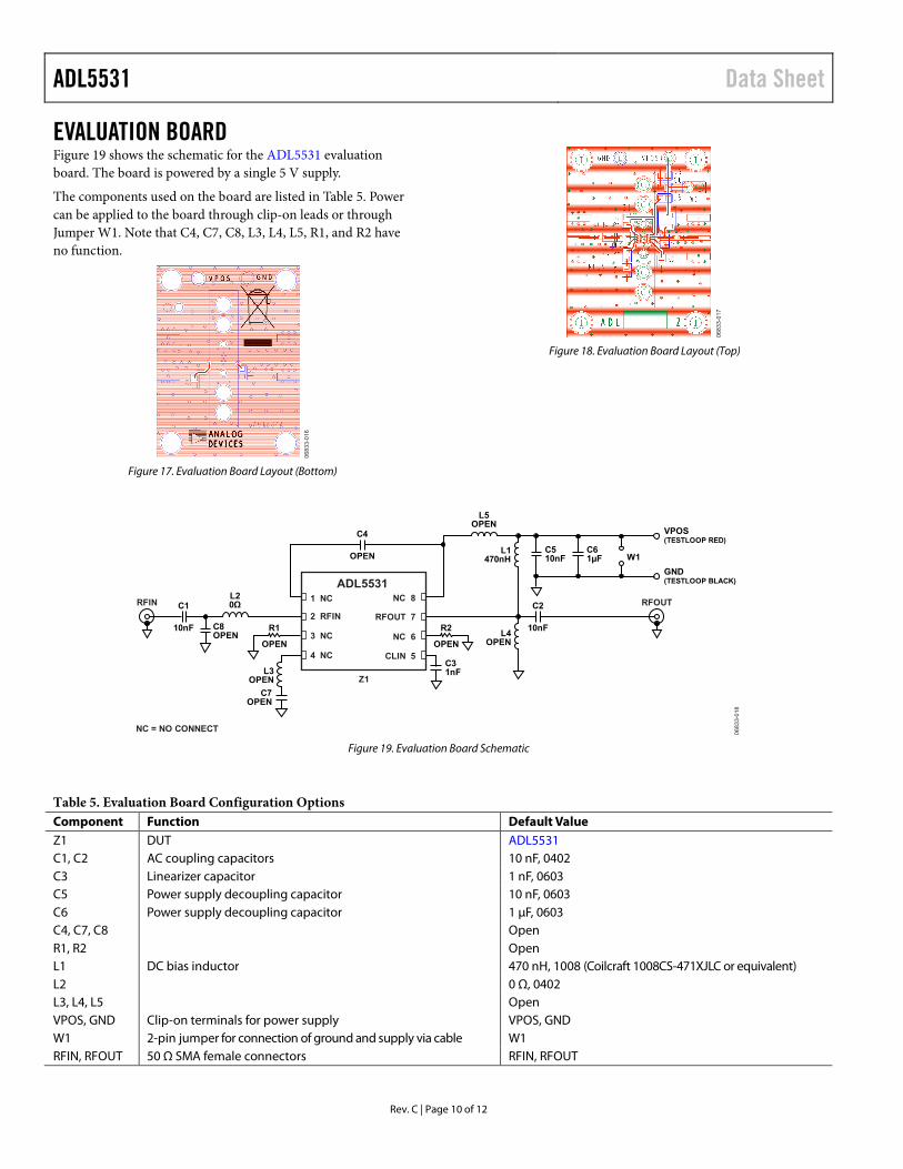
EVALUATION BOARD Figure 19 shows the schematic for the ADL5531 evaluation board. The board is powered by a single 5 V supply.
The components used on the board are listed in Table 5. Power can be applied to the board through clip-on leads or through Jumper W1. Note that C4, C7, C8, L3, L4, L5, R1, and R2 have no function.
0683
3-01
6
Figure 17. Evaluation Board Layout (Bottom)
0683
3-01
7
Figure 18. Evaluation Board Layout (Top)
5CLIN
8NC
NC
NC = NO CONNECT
Z1
RFIN RFOUT
L1470nH
L5OPEN
L4OPEN
4
6NC
RFIN2 7RFOUT
NC3
NCADL5531
0683
3-01
8
1C1
10nF
C31nF
C7OPEN
R2
OPEN
C510nF
C2
10nF
C4
OPEN
C8OPEN
C61µF
L3OPEN
L20Ω
VPOS(TESTLOOP RED)
GND(TESTLOOP BLACK)
W1
R1
OPEN
Figure 19. Evaluation Board Schematic
Table 5. Evaluation Board Configuration Options Component Function Default Value Z1 DUT ADL5531 C1, C2 AC coupling capacitors 10 nF, 0402 C3 Linearizer capacitor 1 nF, 0603 C5 Power supply decoupling capacitor 10 nF, 0603 C6 Power supply decoupling capacitor 1 µF, 0603 C4, C7, C8 Open R1, R2 Open L1 DC bias inductor 470 nH, 1008 (Coilcraft 1008CS-471XJLC or equivalent) L2 0 Ω, 0402 L3, L4, L5 Open VPOS, GND Clip-on terminals for power supply VPOS, GND W1 2-pin jumper for connection of ground and supply via cable W1 RFIN, RFOUT 50 Ω SMA female connectors RFIN, RFOUT

Data Sheet ADL5531
Rev. C | Page 11 of 12
OUTLINE DIMENSIONS
8
1
5
4
0.300.250.20
PIN 1 INDEXAREA
0.800.750.70
1.551.451.35
1.841.741.64
0.203 REF
0.05 MAX0.02 NOM
0.50BSC
EXPOSEDPAD
3.103.00 SQ2.90
FOR PROPER CONNECTION OFTHE EXPOSED PAD, REFER TOTHE PIN CONFIGURATION ANDFUNCTION DESCRIPTIONSSECTION OF THIS DATA SHEET.COPLANARITY
0.08
0.500.400.30
COMPLIANT TOJEDEC STANDARDS MO-229-WEED-4
TOP VIEW BOTTOM VIEW
SIDE VIEW
PKG
-003
886
02-1
0-20
17-A
SEATINGPLANE
PIN 1INDIC ATOR AREA OPTIONS(SEE DETAIL A)
DETAIL A(JEDEC 95)
Figure 20. 8-Lead Lead Frame Chip Scale Package [LFCSP]
3 mm × 3 mm Body and 0.75 mm Package Height CP-8-13
Dimensions shown in millimeters
ORDERING GUIDE Model1 Temperature Range Package Description Package Option Branding ADL5531ACPZ-R7 −40°C to +85°C 8-Lead LFCSP, 7” Tape and Reel CP-8-13 Q16 ADL5531-EVALZ Evaluation Board 1 Z = RoHS Compliant Part.

ADL5531 Data Sheet
Rev. C | Page 12 of 12
NOTES
©2007–2017 Analog Devices, Inc. All rights reserved. Trademarks and registered trademarks are the property of their respective owners. D06833-0-8/17(C)