national open university of nigeria 236-main body.pdf · electronics by treating boolean algebra,...
TRANSCRIPT

NATIONAL OPEN UNIVERSITY OF NIGERIA
COURSE CODE:-CIT 236
COURSE TITLE:-ANALOGUE AND DIGITAL ELECTRONICS

CIT 236 ANALOGUE AND DIGITAL ELECTRONICS
CIT 236ANALOGUE AND DIGITAL ELECTRONICS
Course Writer/Developer Idachaba Francis EnejoNational Open University of Nigeria
Course Coordinator Afolorunso, A. A.National Open University of Nigeria
NATIONAL OPEN UNIVERSITY OF NIGERIA
ii
COURSE GUIDE

CIT 236 ANALOGUE AND DIGITAL ELECTRONICS
National Open University of NigeriaHeadquarters14/16 Ahmadu Bello WayVictoria IslandLagos
Abuja officeNo. 5 Dar es Salaam StreetOff Aminu Kano CrescentWuse II, AbujaNigeria
e-mail: [email protected]: www.nou.edu.ng
Published byNational Open University of Nigeria
Printed 2009
ISBN: 978-058-582-6
All Rights Reserved
iii

CIT 236 ANALOGUE AND DIGITAL ELECTRONICS
CONTENTS PAGE
Introduction............................................................................. 1
What You Will Learn in this Course....................................... 1Course Aims............................................................................ 2 Course Objectives.................................................................... 2 Working through this Course.................................................. 2Course Materials...................................................................... 2Study Units............................................................................. 3 Textbooks and References ...................................................... 3 Assignment File...................................................................... 4 Presentation Schedule.............................................................. 4
Assessment.............................................................................. 4 Tutor-Marked Assignment ...................................................... 4 Examination and Grading........................................................ 5 Course Marking Scheme......................................................... 5
Course Overview………………………………………..….. 6
How to Get the Best from this Course................................... 6Facilitators/Tutors and Tutorials ........................................... 8Summary................................................................................ 9
Introduction
Analogue and Digital Electronics is a 3-credit unit course of eleven units. It is an introductory course which seeks to introduce the students to the basic concepts of analogue and digital electronics. It provides an introduction to the different types of transistors, the biasing arrangements and the configuration of the transistor amplifiers. It also covers the basic principles of feedback and operational amplifiers. The DC power supply is also covered together with voltage regulators heatsinks and finally the text provides an introduction to digital electronics by treating Boolean algebra, logic gates and karnaugh maps. The course is divided into four modules.
Module 1 introduces the transistor, its biasing and the different amplifier configuration of the transistor amplifier. The block lays the foundation for the understanding of the electronics circuit analysis and design.
Module 2 covers the principles of feed back and the operational amplifier. The different types of feedback topolofies and the application
iv

CIT 236 ANALOGUE AND DIGITAL ELECTRONICS
of the different feedback types together with the application of the operational amplifier are covered in this module.
Module 3 describes the DC power supply systems and covers the analysis of the different component parts and it also provides an insight into the design of voltage regulators and heatsinks.
Module 4 has its focus on Digital electronics. It treats the principles of Boolean algebra, logic gates and karnaugh maps. The different types of logic gates and the laws governing Boolean algebra are treated in this module.
The aim of this course is to equip you with the basic skills of analysis and design of electronic circuits as well lay a foundation for the understanding of analogue and digital electronics.
This Course Guide gives you a brief overview of the course content, course duration, and course materials.
What You Will Learn in this Course
The main purpose of this course is to provide the foundational information and theories necessary for the understanding of electronics and the necessary tool for the analysis and design of analogue and digital electronics this, we intend to achieve through the following:
Course Aims
2. Introduces you to the concepts associated with transistors and the transistor amplifiers.
3. Introduces you to the concepts associated with feedback circuits, operational amplifiers and DC power supply design;
4. Expose you to basic principle of Digital electronics, Boolean algebra and logic gates.
Course Objectives
Certain objectives have been set out to ensure that the course achieves its aims. Apart from the course objectives, every unit of this course has set objectives. In the course of the study, you will need to confirm, at the end of each unit, if you have met the objectives set at the beginning of each unit. By the end of this course you should be able to:
i. Identify different types of transistors and the configurations;ii. Describe the design of feed back circuits and the different
feedback topologies.
v

CIT 236 ANALOGUE AND DIGITAL ELECTRONICS
iii. Explain the principles behind the design of operational amplifier based circuit.
iv. Understand the analysis and design of DC power supplies and voltage regulators.
v. Describe the principles and operation of Boolean algebra and the logic gates.
Working through the Course
In order to have a thorough understanding of the course units, you will need to read and understand the contents, practise what you have learnt by studying the network of your organization or proposing one if there is none in existence and be committed to learning and implementing your knowledge.
This course is designed to cover approximately sixteen weeks, and it will require your devoted attention. You should do the exercises in the Tutor-Marked Assignments and submit to your tutors.
Course Materials
These include:
1. Course Guide 2. Study Units 3. Recommended Texts4. A file for your assignments and for records to monitor your
progress. Study Units
There are seventeen study units in this course:
Module 1
Unit 1 Biploar Junction TransistorsUnit 2 Small signal AmplifiersUnit 3 Field Effect Transistors
Module 2
Unit 1 Introduction to feedbackUnit 2 Operational Amplifiers
Module 3
Unit 1 DC power suppliesUnit 2 Voltage regulatorsUnit 3 Heat sinks
vi

CIT 236 ANALOGUE AND DIGITAL ELECTRONICS
Module 4
Unit 1 Boolean AlgebraUnit 2 Logic gatesUnit 3 Karnaugh Maps
Make use of the course materials, do the exercises to enhance your learning.
Textbooks and References
Fitchen F.C; (1972). Transistor Circuit Analysis and Design. Second Edition Van Nostrand Reinhold Publishers.
Maddock R.J and Calcutt D.M (1994). Electronics: a Course for Engineers Second Edition. Longman Publishers.
Neamen D.A (1996). Electronics Circuit Analysis and Design. McGraw-Hill Publishers.
Ron Macini; Op Amps for Everyone. Design Reference, Texas Instruments.
Mendelson, Elliott, (1970). Schaum's Outline of Theory and Problems of Boolean Algebra. McGraw- Hill.
Electronics for Dummies by Gordon McComb and Earl Boysen. ( 2005). Wiley Publishing.
Assignment File
These are of two types: the self-assessment exercises and the Tutor-Marked Assignments. The self-assessment exercises will enable you monitor your performance by yourself, while the Tutor-Marked Assignment is a supervised assignment. The assignments take a certain percentage of your total score in this course. The Tutor-Marked Assignments will be assessed by your tutor within a specified period. The examination at the end of this course will aim at determining the level of mastery of the subject matter. This course includes seventeen Tutor-Marked Assignments and each must be done and submitted accordingly. Your best scores however, will be recorded for you. Be sure to send these assignments to your tutor before the deadline to avoid loss of marks.
Presentation Schedule
The Presentation Schedule included in your course materials gives you the important dates for the completion of tutor marked assignments and
vii

CIT 236 ANALOGUE AND DIGITAL ELECTRONICS
attending tutorials. Remember, you are required to submit all your assignments by the due date. You should guard against lagging behind in your work.
Assessment
There are two aspects to the assessment of the course. First are the tutor marked assignments; second, is a written examination.
In tackling the assignments, you are expected to apply information and knowledge acquired during this course. The assignments must be submitted to your tutor for formal assessment in accordance with the deadlines stated in the Assignment File. The work you submit to your tutor for assessment will count for 30% of your total course mark.
At the end of the course, you will need to sit for a final three-hour
examination. This will also count for 70% of your total course mark.
Tutor-Marked Assignment
There are seventeen tutor marked assignments in this course. You need to submit all the assignments. The total marks for the best four (4) assignments will be 30% of your total course mark.
Assignment questions for the units in this course are contained in the
Assignment File. You should be able to complete your assignments
from the information and materials contained in your set textbooks,
reading and study units. However, you may wish to use other references
to broaden your viewpoint and provide a deeper understanding of the
subject.
When you have completed each assignment, send it together with form
to your tutor. Make sure that each assignment reaches your tutor on or
before the deadline given. If, however, you cannot complete your work
on time, contact your tutor before the assignment is done to discuss the
possibility of an extension.
Examination and Grading
viii

CIT 236 ANALOGUE AND DIGITAL ELECTRONICS
The final examination for the course will carry 70% of the total marks available for this course. The examination will cover every aspect of the course, so you are advised to revise all your corrected assignments before the examination.
This course endows you with the status of a teacher and that of a learner. This means that you teach yourself and that you learn, as your learning capabilities would allow. It also means that you are in a better position to determine and to ascertain the what, the how, and the when of your course learning. No teacher imposes any method of leaning on you.
The course units are similarly designed with the introduction following the table of contents, then a set of objectives and then the concepts and so on.
The objectives guide you as you go through the units to ascertain your knowledge of the required terms and expressions.
Course Marking Scheme
This table shows how the actual course marking is broken down.
Assessment MarksAssignment 1- 4 Four assignments, best three marks of the
four count at 30% of course marksFinal Examination 70% of overall course marks Total 100% of course marks
Table 1: Course Marking Scheme
Course Overview
Unit Title of Work WeeksActivity
Assessment(End of Unit)
Course Guide Week 1 Module 1
1 Bipolar Junction Transistors Week 1-2 Assignment 12 Small Signal Amplifiers Week 3 Assignment 23 Field Effect Transistors Week 4 Assignment 3
Module 21 Introduction to Feedback Week 5-6 Assignment 4
ix

CIT 236 ANALOGUE AND DIGITAL ELECTRONICS
2 Operational Amplifiers Week 7-8 Assignment 5 Module 3
1 Dc power Supplies Week 9-10
2 Voltage Regulators Week 113 Heat Sink Design Week 12 Assignment 6
Module 4 1 Boolean Algebra Week 13 Assignment 72 Logic Gates Week 14 Assignment 83 Karnaugh Maps Week 15
Revision Week 16Examination Week 17Total 17 weeks
How to Get the Best from this Course
In distance learning the study units replace the university lecturer. This is one of the great advantages of distance learning; you can read and work through specially designed study materials at your own pace, and at a time and place that suit you best. Think of it as reading the lecture instead of listening to a lecturer. In the same way that a lecturer might set you some reading to do, the study units tell you when to read your set books or other material. Just as a lecturer might give you an in-class exercise, your study units provide exercises for you to do at appropriate points.
Each of the study units follows a common format. The first item is an introduction to the subject matter of the unit and how a particular unit is integrated with the other units and the course as a whole. Next is a set of learning objectives. These objectives enable you know what you should be able to do by the time you have completed the unit. You should use these objectives to guide your study. When you have finished the units you must go back and check whether you have achieved the objectives. If you make a habit of doing this you will significantly improve your chances of passing the course.
Remember that your tutor’s job is to assist you. When you need help, don’t hesitate to call and ask your tutor to provide it.
1 Read this Course Guide thoroughly.
2 Organize a study schedule. Refer to the ‘Course Overview’ for more details. Note the time you are expected to spend on each unit and how the assignments relate to the units. Whatever method you chose to use, you should decide on it and write in your own dates for working on each unit.
x

CIT 236 ANALOGUE AND DIGITAL ELECTRONICS
3 Once you have created your own study schedule, do everything you can to stick to it. The major reason that students fail is that they lag behind in their course work.
4 Turn to Unit 1 and read the introduction and the objectives for the unit.
5 Assemble the study materials. Information about what you need for a unit is given in the ‘Overview’ at the beginning of each unit. You will almost always need both the study unit you are working on and one of your set of books on your desk at the same time.
6 Work through the unit. The content of the unit itself has been arranged to provide a sequence for you to follow. As you work through the unit you will be instructed to read sections from your set books or other articles. Use the unit to guide your reading
7 Review the objectives for each study unit to confirm that you have achieved them. If you feel unsure about any of the objectives, review the study material or consult your tutor.
8 When you are confident that you have achieved a unit’s objectives, you can then start on the next unit. Proceed unit by unit through the course and try to pace your study so that you keep yourself on schedule.
9 When you have submitted an assignment to your tutor for marking, do not wait for its return before starting on the next unit. Keep to your schedule. When the assignment is returned, pay particular attention to your tutor’s comments, both on the tutor-marked assignment form and also written on the assignment. Consult your tutor as soon as possible if you have any questions or problems.
10 After completing the last unit, review the course and prepare yourself for the final examination. Check that you have achieved the unit objectives (listed at the beginning of each unit) and the course objectives (listed in this Course Guide).
Facilitators/Tutors and Tutorials
There are 12 hours of tutorials provided in support of this course. You will be notified of the dates, times and location of these tutorials, together with the name and phone number of your tutor, as soon as you are allocated a tutorial group.
xi

CIT 236 ANALOGUE AND DIGITAL ELECTRONICS
Your tutor will mark and comment on your assignments, keep a close watch on your progress and on any difficulties you might encounter and provide assistance to you during the course. You must mail or submit your tutor-marked assignments to your tutor well before the due date (at least two working days are required). They will be marked by your tutor and returned to you as soon as possible.
Do not hesitate to contact your tutor by telephone, or e-mail if you need help. The following might be circumstances in which you would find help necessary. Contact your tutor if:
• you do not understand any part of the study units or the assigned readings,
• you have difficulty with the self-tests or exercises,• you have a question or problem with an assignment, with your tutor’s
comments on an assignment or with the grading of an assignment.
You should try your best to attend the tutorials. This is the only chance to have face to face contact with your tutor and to ask questions which are answered instantly. You can raise any problem encountered in the course of your study. To gain the maximum benefit from course tutorials, prepare a question list before attending them. You will learn a lot from participating in discussions actively.
Summary
Analogue and Digital Electronics introduces you to the basic concepts of analogue and digital electronics. It provides an introduction to the different types of transistors, the biasing arrangements and the configuration of the transistor amplifiers. It also covers the basic principles of feedback and operational amplifiers. The DC power supply is also covered together with voltage regulators heatsinks and finally the text provides an introduction to digital electronics by treating Boolean algebra, logic gates and karnaugh maps. The content of the course material was planned and written to ensure that you acquire the proper knowledge and skills for the appropriate situations. Real-life situations have been created to enable you identify with and create some of your own. The essence is to get you to acquire the necessary knowledge and
xii

CIT 236 ANALOGUE AND DIGITAL ELECTRONICS
competence, and by equipping you with the necessary tools, we hope to have achieved that.
I wish you success with the course and hope that you will find it both
interesting and useful.
xiii

CIT 236 ANALOGUE AND DIGITAL ELECTRONICS
Course Code CIT 236
Course Title Analogue and Digital Electronics
Course Writer/Developer Idachaba Francis EnejoNational Open University of Nigeria
Course Coordinator Afolorunso, A. A.National Open University of Nigeria
NATIONAL OPEN UNIVERSITY OF NIGERIA
xiv

CIT 236 ANALOGUE AND DIGITAL ELECTRONICS
National Open University of NigeriaHeadquarters14/16 Ahmadu Bello WayVictoria IslandLagos
Abuja officeNo. 5 Dar es Salaam StreetOff Aminu Kano CrescentWuse II, AbujaNigeria
e-mail: [email protected]: www.nou.edu.ng
Published byNational Open University of Nigeria
Printed 2009
ISBN: 978-058-582-6
All Rights Reserved
Printed by:
xv

CIT 236 ANALOGUE AND DIGITAL ELECTRONICS
CONTENTS PAGE
Module 1 …………………………………….……… 1
Unit 1 Bipolar Junction Transistors…………………..…. 1Unit 2 Small Signal Amplifiers………………………..… 19Unit 3 Field Effect Transistors………………………..…. 31
Module 2 ………………………………………………..…. 39
Unit 1 Introduction to Feedback………………………… 39Unit 2 Operational Amplifiers (OPAMPS)……………… 51
Module 3 ……………………………….………………….. 60
Unit 1 DC Power Supplies……………………………….. 60Unit 2 Voltage Regulators……………………………….. 76Unit 3 Heat Sinks………………………………………… 92
Module 4 ………………………………..…………………. 97
Unit 1 Boolean Algebra………………………………….. 97Unit 2 Logic Gates………………………………………. 102Unit 3 Karnaugh Map……………………………………. 111
xvi

CIT 236 ANALOGUE AND DIGITAL ELECTRONICS
MODULE 1
Unit 1 Bipolar Junction TransistorsUnit 2 Small Signal AmplifiersUnit 3 Field Effect Transistors
UNIT 1 BIPOLAR JUNCTION TRANSISTORS
CONTENTS
1.0 Introduction2.0 Objectives3.0 Main Content
3.1 Bipolar Junction Transistor3.2 Bipolar Junction Transistor Configurations3.3 Load Lines3.4 Bipolar Junction Transistor Biasing3.5 Common Emitter Biasing
4.0 Conclusion5.0 Summary6.0 Tutor-Marked Assignment7.0 References/Further Readings
1.0 INTRODUCTION
A transistor is a three-terminal semiconductor device that can be used for amplification and switching. Amplification consists of magnifying a signal by transferring energy to it from an external source; whereas a transistor switch is a device for controlling a relatively large current between or voltage across two terminals by means of a small control current or voltage applied at a third terminal. There are two major families of transistors are bipolar junction transistors, or BJTs; and field-effect transistors, or FETs. As will be shown, the BJT acts essentially as a current-controlled device, while the FET behaves as a voltage-controlled device.
2.0 OBJECTIVES
At the end of this unit, students should be able to:
• be able to IDENTIFY basic transistor amplifier topologies • be able to ANALYZE basic amplifier topologies for gains and
resistances• be able to DISCUSS the relative properties of various amplifier
topologies• be able to DESIGN basic amplifiers to meet or exceed stated
specifications.
1

CIT 236 ANALOGUE AND DIGITAL ELECTRONICS
3.0 MAIN CONTENT
3.1 The Bipolar Junction Transistor (BJT)
The pn junction forms the basis of a large number of semiconductor devices. A BJT is formed by joining three sections of semiconductor material, each with a different doping concentration. The three sections can be either a thin nregion sandwiched between p+ and p layers, or a p region between n and n+ layers, where the superscript “plus” indicates more heavily doped material. The resulting BJTs are called pnp and npn transistors, respectively:
The figure 1.1 below shows the block diagrams and circuit symbols of both the npn ad the pnp transistors.
Figure 1.1 transistor symbols
Figure 1.2 electron flows in transistors
The operation of the npn BJT can be explained by considering the transistor as consisting of two back-to-back pn junctions. The base-emitter (BE) junction acts very much like a diode when it is forward-
2

CIT 236 ANALOGUE AND DIGITAL ELECTRONICS
biased; thus, the corresponding flow of hole and electron currents from base to emitter when the collector is open and the BE junction is forward-biased, is shown in figure 1.2.Note that the electron current has been shown larger than the hole current, because of the heavier doping of the n side of the junction. Some of the electron-hole pairs in the base will recombine; the remaining charge carriers will give rise to a net flow of current from base to emitter. It is also important to observe that the base is much narrower than the emitter section of the transistor.
The flow of electrons in the transistor is represented by the equation below.
IE = IB + IC ……………………………………………………………..1
Since the transistor is biased in the active region a small base current controls the much larger collector current.
Where IC = βIB…………………………………………………………..2
where β is a current amplification factor dependent on the physical properties of the transistor. Typical values of β range from 20 to 200. The operation of a pnp transistor is completely similar to that of the npn device, with the roles of the charge carriers (and therefore the signs of the currents) reversed.
BBE III β+= …………………………………………………………….3BE II )1( β+= ………………...………………………………………….4
from the equation (4) above
)1( β+= E
BII ………………………………………………….…………5
EC II
+=
ββ
1 …………….…………………………..……….………6
Equation 6 can be written as EC II α=
Thus
+=
ββα
1 where α = common base current gain.
3

CIT 236 ANALOGUE AND DIGITAL ELECTRONICS
3.2 Bipolar Junction Transistor Configurations
Transistors can be configured in three different modes with one pair of terminals for the input and another pair for the output. These configurations are:
1. Common emitter 2. Common collector3. Common base.
• Common Emitter
In the common emitter configuration, the input terminal is the base while the output terminal is the collector and the emitter is common to both the input and the output as shown in figure 1.3 below.
Figure 1.3 Common Emitter configurations
The current gain for this configuration is given by B
C
II
currentinputcurrentoutput =
__
• Common Collector
In the common collector configuration, the input terminal is the base while the output terminal is the emitter and the collector is common to both the input and the output as shown in figure 3.4 below.
Figure 1.4 Common collector configurations
The current gain for this configuration is given by B
E
II
4

CIT 236 ANALOGUE AND DIGITAL ELECTRONICS
• Common Base
In the common base configuration, the input terminal is the emitter while the output terminal is the collector and the base is common to both the input and the output as shown in figure 1.5 below
Figure 1.5 common base configuration
The current gain for this configuration is given by E
C
II
The gain for the CB configuration is always less than 1, so the CB configuration is not used for current amplification .The CC and CE configurations both have a high gain but the input impedance of the CE configuration is higher than that of the CC. This makes the CE configuration the preferred choice for amplifiers in circuit design.
3.3 Loads Lines
The load line is a line drawn based on the DC operating characteristics of the circuit. It enables the visualization of the transistor characteristics. It is determined by using the DC equations of the circuit. The Ic (max) and Vce (max) are used to determine the end points of the line, these points are then joined together and superimposed on the transistor characteristics.
5

CIT 236 ANALOGUE AND DIGITAL ELECTRONICS
Figure 1.6 Amplifier circuit
From the circuit 1.6, the analysis is done below
From the output equation
V I R Vcc C C CE= +
The load line is determined by identifying the two endpoints of the line.The are determined by assuming VCE = 0 and finding Ic, and the V subscribe is determined by assuming Ic= 0.
From the output equation, with Ic = 0,
Vcc = VCE
With VCE = 0
Vcc = IcRc
Ic(max) =Rc
Vcc
The load line is sketched in the figure 1.7 below
6

CIT 236 ANALOGUE AND DIGITAL ELECTRONICS
Figure 1.7 load line
The curves are generated at different base currents. The Q point (operating Point) is the intersection of the Ic and the Vce on the load line for any particular base current.
From the graphs, as Ic rises from 0, the mode of operation of the transistor changes from cutoff to active and when the Ic gets to the maximum, the transistor gets to the saturation region of operation.
Example 1
Given the circuit below, determine the load line.
From the output equation
V I R Vcc C C CE= +
With Vce = 0
Ic(max) = mAK
5.2410 =
With Ic = 0
7

CIT 236 ANALOGUE AND DIGITAL ELECTRONICS
Vce = 10V
3.4 Bipolar Junction Transistor Biasing
The transistor can serve either as a switch or an amplifier. The mode of operation of each transistor is determined by the bias condition in which it operates.
Biasing can be defined as the setting up of the DC voltages and current in an electronic circuit.
From the output characteristics, the transistor has 3 regions of operation.
(i) Saturation region(ii) Active region(iii) Cutoff region
Figure 1.8 Q-point
The Q point or dc operating point is that point on the load line where the Icq and Vceq intercept on the load line. The transistor when operating as a switch is biased in the saturation or cutoff region but for the transistor to be used as an amplifier it is biased in the active region. With transistor in the forward active region the voltage across the B-E junction is V subscribe (on) is 0.7V for silicon transistors and 0.4V for germanium transistors.
The determination of the q point is through the process of biasing.
8

CIT 236 ANALOGUE AND DIGITAL ELECTRONICS
Example 2
Calculate the base, collector and emitter currents for the circuit shown below.β =200
From the output equation
Vcc = IcRc + VCE
From the input equation
VBB= IBRB + VBE
IB = AKR
VVB
BEBB µ15220
7.04 =−=−
Ic = βIB = (200)(15μA) = 3mA
IE = (1+β). IB = (200+1) (15μA) = 3.02mA
VCE = Vcc – IcRc = 10 – (3mA)(2K) = 4V
3.5 Types Common Emitter Biasing
There are different types of bias circuit with each having its advantages and disadvantages.
1. Base Bias
This is the simplest type and is also known as fixed bias. The quiescent base current is established by a single base resistor as shown in figure 1.9 below.
9

CIT 236 ANALOGUE AND DIGITAL ELECTRONICS
Figure 1.9 base bias
Biasing of this circuit will involve the selection of appropriate values for the base resistance and collector resistance.
Analysis
Input equationV I R VI R V V
cc B B BE
B B CC BE
= += −
IV V
R
RV V
I
BQCC BE
B
BCC BE
BQ
=−
=−
This equation yields the Quiescent base current IBQ
From the circuit, the output equation is derived below
V I R Vcc C C CE= +
I R V VCQ C CC CE= −
IV V
RCQ
CC CE
C=
−
RV V
IC
CC CE
CQ=
−
Example 3
Given the circuit below, design the amplifier for the following specifications:
10
(2)
(1)
(3)
(4)
(5)
(6)
(7)
(8)

CIT 236 ANALOGUE AND DIGITAL ELECTRONICS
VCC = 12V, β = 100, Vbe = 0.7, Icq = 1mA Vceq = 6V
Solution
From the input equation,
V I R VCC B B BE= +
I R V VI R II VB B CC BE
B B
= − = −=
12 0 73
..
From the output equation
V I R VI R V V
IcmA
K
cc c c ce
c c cc ce
= += − = −
=−
=
12 612 61
6 Ω
IcqI
IIcq mA
A
BQ
BQ
=
∴ = = =
β
βµ
1100
10
The base resistance is determined from the input equation to be
I R V V on
RA
M
BQ B CC be
B
= −
=−
=
( ).
.12 0 710
113µ
Ω
The load line is determined to be
11

CIT 236 ANALOGUE AND DIGITAL ELECTRONICS
Vcc IcRc VceIcVce Vcc VVce
IcVccRc K
mA
= +=
= ==
= = =
012
0126
2
,
From the various formulas used above, the Icq is dependent to a large extent on the β. The beta (β) varies with temperature so any circuit built with too much dependence on β will be very unstable.
• Base Bias with Collector Feedback
The base is connected to the collector as shown in the circuit in figure 1.10 below
Figure 1.10 Base bias with collector feedback
Output equationCECBCCC VRIIV ++= )( …………………………………………………..1
The collector current and the base currents flow through the collector resistor
But IC >> IB
IC(sat) =Rc
Vcc
Since there is no emitter resistor the out put equation becomes
CCBCCC VRIIV ++= )(
CBCC RIIVccV )( +−=
Since Vc also forms part of the input equation, the input equation becomes
12

CIT 236 ANALOGUE AND DIGITAL ELECTRONICS
BEBBC VRIV +=
CBC RIIVcc )( +− BEBB VRI +=
Since IC >> IB
CC RIVcc − BEBB VRI +=
But IB= βIc
CCBEB RIVccVIcR −=+
β
The collector current can be derived from the expression below.
EB
BE IRcR
VVccIc ≈
+
−=
β
From the expression for collector current, the effect of the transistor gain on the collector current is reduced leading to better system stability
• Base Bias with Collector and Emitter Feedback
Figure 1.11 Base Bias with collector and emitter feedback
13

CIT 236 ANALOGUE AND DIGITAL ELECTRONICS
From the output equation
EECECBCCC RIVRIIV +++= )(
IC>>IB and IC = IE
)( ECCCEECCECCCC RRIVRIVRIV ++=++=
)( CE
CECCC RR
VVI+−=
At saturation (VCE =0)
)( CE
CCC RR
VI+
=
The actual value of Ic is derived using the input equation since in most cases the VCE is unknown
From the input equation
EEBBBECCCC RIRIVRIV +++=
Since IC = IE
ECBBBECCCC RIRIVRIV +++=
BBECCBECC RIRRIVV ++=− )(
But βC
BII =
βB
ECCBECCRRRIVV ++=− )(
)(β
BCE
BECCC RRR
VVI++
−=
Example 4
Determine the Ic(sat),VCE and Vc. In the circuit below. Neglect VBE
14

CIT 236 ANALOGUE AND DIGITAL ELECTRONICS
From the output equation
EECECBCCC RIVRIIV +++= )(
IC>>IB and IC = IE
)( ECCCEECCECCCC RRIVRIVRIV ++=++=
)( CE
CECCC RR
VVI+−=
At saturation (VCE =0)
mAKK
satIC 11.0)10100(
12)( =+
=
VC = VCE + VE
)( ECCCCCE RRIVV +−=
VE =IERE
To determine IC we use the input equation
EEBBBECCCC RIRIVRIV +++=
Since IC = IE
ECBBBECCCC RIRIVRIV +++=
BBECCBECC RIRRIVV ++=− )(
15

CIT 236 ANALOGUE AND DIGITAL ELECTRONICS
But βC
BII =
βB
ECCBECCRRRIVV ++=− )(
)(β
BCE
BECCC RRR
VVI++
−=
kkkkIC 115
12
)10050010010(
12 =++
==0.1mA
Substituting the value of IC in the equation for VCE we have
VKmARRIVV ECCCCCE 1)110(1.012)( =−=+−=
VC = VCE + VE =1 +ICRE = 1 + 0.1mA(100K) =11V
• Voltage Divider Bias
From the circuit diagram in figure 1.12, the voltage divider bias is analyzed below as follows.
Figure 1.12 Voltage divider bias
From the potential (voltage) divider equation
212*
RRRVccVB
+=
VB = Vbe + VE
16

CIT 236 ANALOGUE AND DIGITAL ELECTRONICS
VE = VB – Vbe but VB >>Vbe
IE = REVB
REVbeVB
REVE =−=
From the output equationEECECCCC RIVRIV ++=
VC = VCE + VE
)( CECCCCE RRIVV +−=
With VCE = 0 in the output equation, Ic is determined as
IC(sat) =CE RR
Vcc+
The base voltage is set by the resistors R1 and R2 thus the effect of the transistor forward gain is reduced .The D.C bias is independent of β.
4.0 CONCLUSION
In this unit you have been introduced to the transistor amplifier and the different types of biasing arrangements and transistor configurations.
5.0 SUMMARY
In this unit we have been able to extend knowledge of the theory and applications of transistors and transistor amplifier design.
6.0 TUTOR-MARKED ASSIGNMENT
1. Determine the VCE and IC in the circuit diagram shown below. Vbe = 0.7
17

CIT 236 ANALOGUE AND DIGITAL ELECTRONICS
2. Given the circuit below, design the amplifier for the following specifications:
VCC = 12V, β = 100, Vbe = 0.7, Icq = 1mA Vceq = 6V
7.0 REFERENCES/FURTHER READINGS
Fitchen F.C; (1972). Transistor Circuit Analysis and Design. Second Edition Van Nostrand Reinhold Publishers.
Maddock R.J and Calcutt D.M (1994). Electronics: a Course for Engineers Second Edition. Longman Publishers.
Neamen D.A (1996). Electronics Circuit Analysis and Design. McGraw-Hill Publishers.
18

CIT 236 ANALOGUE AND DIGITAL ELECTRONICS
UNIT 2 SMALL SIGNAL AMPLIFIERS
CONTENTS
1.0 Introduction2.0 Objectives3.0 Main Content
3.1 Transistor Hybrid Parameters3.2 Analysis of a Single Stage Transistor Amplifier Small
Signal Operation3.3 Input Impedance3.4 Output Impedance3.5 Voltage Gain3.6 Effect of Bypass Capacitor on Common Emitter Amplifier
4.0 Conclusion5.0 Summary6.0 Tutor-Marked Assignment7.0 References/ Further Readings
1.0 INTRODUCTION
Electronic amplifying devices such as BJT and FET have three terminals (E,B,C and S,G,D).In a basic amplifying circuit, one of the terminals is made common while the other two serve as input and output ports. Small-signal models for the BJT take advantage of the relative linearity of the base and collector curves in the vicinity of an operating point. These linear circuit models work very effectively, providing that the transistor voltages and currents remain within some region around the operating point. This condition is usually satisfied in small-signal amplifiers used to magnify low-level signals (e.g., sensor signals). For the purpose of our discussion, we use the hybrid-parameter (h-parameter) small-signal model of the BJT, to be discussed presently. Note that a small-signal model assumes that the DC bias point (Q-point) of the transistor has been established. The following convention will be used: each voltage and current is assumed to be the superposition of a DC component (the quiescent voltage or current) and a small-signal AC component. The former is denoted by an uppercase letter and the latter by an uppercase letter preceded by the symbol Δ. Thus,
iB = IBQ + Δ IB
iC = ICQ + Δ IC
vCE = VCEQ + Δ VCE
19

CIT 236 ANALOGUE AND DIGITAL ELECTRONICS
2.0 OBJECTIVES
At the end of this unit, student should be able to:
• be able to IDENTIFY the transistor hybrid parameters • be able to ANALYZE amplifier topologies for gains and impedances• be able to DISCUSS the relative properties of various amplifier
configurations• be able to DESIGN basic amplifiers to meet or exceed stated
specifications.
3.0 MAIN CONTENT
3.1 Transistor Hybrid parameters
The Hybrid parameters are specifications used in the analysis of transistor amplifiers there are four h parameters and these are:
• The parameter hie which is approximately equal to the ratio Δ VBE/ΔIB. Physically, this parameter represents the forward resistance of the BE junction.
• The parameter hre which is representative of the fact that the IB-VBE curve is slightly dependent on the actual value of the collector-emitter voltage, VCE. However, this effect is virtually negligible in any applications of interest to us. Thus, we shall assume that hre ≈ 0. A typical value of hre for VCE ≥ 1 V is around 10-2.
• The parameter hf e is the current ratio Δ IC /ΔIB. This parameter represents the current gain of the transistor and is approximately equivalent to the parameter β introduced earlier. For the purpose of our discussion, β and hf e will be interchangeable, although they are not exactly identical.
• The parameter hoe may be calculated as hoe = ΔIC/ Δ VCE From the
collector characteristic curves. This parameter is a physical indication of the fact that the IC-VCE curves in the linear active region are not exactly flat; hoe represents the upward slope of these curves and therefore has units of conductance (S). Typical values of hoe are around 10-5 S. this parameter is often assumed to be negligible.
20

CIT 236 ANALOGUE AND DIGITAL ELECTRONICS
3.2 Analysis of a Single Stage Transistor Amplifier Small Signal Operation
In order to fully analyze a transistor amplifier, the analysis is broken into AC and DC analysis. In the DC analysis all capacitors are regarded as open circuits, while for the AC analysis, the capacitors are regarded as short circuits and the DC source is replaced by a ground.
The purpose of the analysis is to determine the different specifications of the circuit. These specifications include the input impedance, output impedance and the circuit gain.
Example 1
Given the circuit below, determine the Q point voltage and current values and AC open-loop voltage gain of the amplifier of Figure 2.1; the amplifier employs a 2N5088 npn transistor. β=350
Figure 2.1
21

CIT 236 ANALOGUE AND DIGITAL ELECTRONICS
• Analysis
Q-point calculation
We first write the collector circuit equation by applying KVL:
VCC = VCE + RCIC + REIE = VCE + RCIC + RE(IB + IC)
≈ VCE + (RC + RE)IC
where the emitter current has been approximately set equal to the collector current since the current gain is large and IC >> IB.
Next, we write the base circuit equation, also via KVL:
VBB = RBIB + VBE + REIE = (RB + (β + 1)RE)IB + Vbe
The above equation can be solved numerically (with hf e = β) to obtain:
ARR
VVIEB
BEBBB µ
β40
100351101006.06
)1( 3 =×+×
−=++
−=
Then,
IC = βIB = 350 X 40 x 10-6 = 14 mA
And
VCE = VCC − (RC + RE)IC = 12 − 600 x 40 x 10-3 = 3.6 V
Thus, the Q point for the amplifier is:
IBQ = 40 μA, ICQ = 14 mA and VCEQ = 3.6 V
Confirming that the transistor is indeed in the active region.
From previous discussion, it has been verified that the common emitter configuration is the best for signal amplification. We shall be looking at the single stage common emitter amplifier.
Any amplifier circuit has the following parts:
1) The Bias Circuit2) The Load Circuit3) The Coupling Circuit
22

CIT 236 ANALOGUE AND DIGITAL ELECTRONICS
The bias circuit has been discussed so we focus on the other component parts.
Fig 2.2: CE amplifier circuit
From the diagram above, the following are the responsibility of the different components.
C = Coupling capacitor. it prevents dc signals in the source from upsetting the amplifier’s Q point values.
R1 and R2 = potential divider bias resistors
RC = load/collector resistor
RE = Emitter resistor
Given a common emitter amplifier circuit, to analyze such a circuit we need to consider its DC and AC characteristics.
Example 2
Given the circuit with the following parameters below, (βdc =150 and βac = 160)
Where βdc =DC gain and βac = AC gain. Determine the circuit specifications given the following component parameters. RE = 600Ω Rc = 1kΩ R1 = 22kΩ R2= 4.7kΩ
23

CIT 236 ANALOGUE AND DIGITAL ELECTRONICS
Fig 2.3: CE amplifier circuit
In order to understand the operation of the circuit given above, we will have to perform both the DC and AC analysis.
• DC Analysis
Before the DC analysis is performed, all coupling capacitors are regarded as open circuit. This will yield the following representation of the circuit above.
Fig 2.4:
24

CIT 236 ANALOGUE AND DIGITAL ELECTRONICS
From Ohms Law,
IinVinRin =
Vin =Vbe + IERE . Vbe = 0.7 for silicon transistor which is the most widely used type. IERE >> Vbe
Vin = IERE
IinRI
Rin EE=
EE RIIinRinVin == but IE ≈ Ic = βIb . The base current Ib is the input current and RIN is the resistance at the base so,
Iin = Ib and RIN = RB
EIbRVin β= =IbRB
IbIbRRB Eβ= canceling Ib from both the numerator and denominator we
have the DC input resistance RB to be, ERRB β=
Inserting the values of the components,The Dc input resistance of the circuit is give by
RIN = EdcRRB β= =150 x 600 = 90KΩ
Note: If RB is more than 10 times R2 then the voltage divider rules is used
Vxkk
kVccRR
RVB 11.2127.422
7.421
2 =
+=
+=
VE =VB –Vbe =2.11 – 0.7=1.41V
IE = mAREVE 4.2
60041.1 ==
Since Ic =IE
VC = Vcc- IcRC = 12 – 2.4 = 9.6V
VCE = VC –VE = 9.6 – 1.41 = 8.19V
25

CIT 236 ANALOGUE AND DIGITAL ELECTRONICS
• AC Analysis
For the ac analysis the circuit is redrawn with the following assumptions.
1. All capacitors are short circuit
2. DC sources are replaced by ground
This circuit is further reduced to the circuit shown below
Rin (base) is the resistance at the base of the transistor and it is derived with the ac emitter resistance added in series to the RE.
Rin (base) = βac(re + RE)
The ac emitter resistance is given by IEmVre 25=
3.3 Input Impedance
The total input impedance of the circuit is the parallel combination of R1 ,R2 and Rin(base).Thus the circuit is reduced to the following
26

CIT 236 ANALOGUE AND DIGITAL ELECTRONICS
Input Impedance = R1//R2//Rin(base).
From the component values of the circuit assuming a source impedance of 300Ω, the input impedance is computed to be
Rin(base) = 160(re + 600)
But mAmV
IEmVre
4.22525 == =10.4Ω
IE is the DC emitter current computed to be 2.4mA.
Rin (base) = 160 (10.4 + 600)
Rin(base) =160(610.4) = 97664 Ω
The voltage at the base of the transistor (Vb) is determined below
If RS << Rin(input impedance) then Vb = Vin. If not then the voltage divider equation is used as shown below.
VinRinRS
RinVb
+=
27

CIT 236 ANALOGUE AND DIGITAL ELECTRONICS
Compute the input impedance and the voltage at the base of the transistor
3.4 Output Impedance
The output resistance looking at the collector is approximately equal to RC. In situations where a load is connected in parallel with the RC, the output resistance will be equal to the parallel combination of both the Rc and the load resistance. Thus a load (RL) connected to the output affects the gain.
RC1=RC//RL
3.5 Voltage Gain
The voltage gain is the ratio between the output voltage and the input voltage.
)(
)(
)(
__
REreRCAV
REreIEIERC
REreIEIcRC
VbVC
voltageInputvoltageOutputAV
+=
+
+=
=
This is the voltage gain from the base to the collector of the transistor.
The total circuit gain is made up of the attenuation due to the source resistance and the base to collector gain as shown below.
VinRinRS
RinVb
+=
28

CIT 236 ANALOGUE AND DIGITAL ELECTRONICS
+=
VinVb
REreRCAV I
)(
3.6 Effects of Emitter Bypass Capacitor on the CE Amplifier
When a capacitor is connected across the emitter resistor it bypasses the RE as the capacitor acts as a sort circuit for the AC signals. Thus the Ac voltage gain becomes
)(reRCAV = RE is neglected and the gain increases.
This increase in gain however leads to a reduction in gain stability because the re ( ac emitter resistance varies with temperature)
4.0 CONCLUSION
In this unit you have been introduced to the small signal operation of the BJT amplifier and the transistor hybrid parameters.
5.0 SUMMARY
In this unit we have been able to extend knowledge of the theory and applications of transistors and small signal transistor amplifier design.
6.0 TUTOR-MARKED ASSIGNMENT
1. Determine the Q point of the amplifier shown below. Vbe = 0.7 V; β = 100; VCC = 15
V.R1 = 68 k_; R2 = 11.7 k_; RC = 200 _; RE = 200 _.
2. Given the amplifier circuit below determine the total output voltage (ac and dc).Vcc = 10V, βdc=150, β = 175 RS = 300Ω,R1 =50KΩ,R2 = 10KΩ, Rc = 5KΩ,
29

CIT 236 ANALOGUE AND DIGITAL ELECTRONICS
RE1=RE2 = 500Ω, Load =50KΩ
7.0 REFERENCES/FURTHER READINGS
Fitchen F.C; (1972). Transistor Circuit Analysis and Design. Second Edition Van Nostrand Reinhold Publishers.
Maddock R.J and Calcutt D.M (1994). Electronics: a Course for Engineers Second Edition. Longman Publishers.
Neamen D.A (1996). Electronics Circuit Analysis and Design. McGraw-Hill Publishers.
30

CIT 236 ANALOGUE AND DIGITAL ELECTRONICS
UNIT 3 FIELD EFFECT TRANSISTORS
CONTENTS
1.0 Introduction2.0 Objectives3.0 Main Content
3.1 Junction Field Effect Transistors3.2 FET Configurations
4.0 Conclusion5.0 Summary6.0 Tutor-Marked Assignment7.0 References/Further Readings
1.0 INTRODUCTION
The concept upon which the field - effect transistor or FET is based is that the width of a conducting channel in a semiconductor may be varied by the external application of an electric field. Thus, FETs behave as voltage-controlled resistors. These devices can be grouped into three major categories. The first two categories are both types of metal-oxide-semiconductor field-effect transistors,or MOSFETs: enhancement-mode MOSFETs and depletion-mode MOSFETs. The third category consists of junction field-effect transistors, or JFETs. In addition, each of these devices can be fabricated either as an n-channel device or as a p-channel device, where the n or p designation indicates the nature of the doping in the semiconductor channel.
2.0 OBJECTIVES
At the end of this unit, students are expected be able to:
• be able to IDENTIFY field effect transistor symbols • be able to ANALYZE basic FET amplifier topologies for gains and
resistances• be able to DISCUSS the relative properties of various FET
configurations• be able to DESIGN basic amplifiers to meet or exceed stated
specifications.
31

CIT 236 ANALOGUE AND DIGITAL ELECTRONICS
3.0 MAIN CONTENT
3.1 Junction Field Effect Transistors
There are two general classes of FETs
(i) The Metal Oxide Semiconductor FET (MOSFET)(ii) The Junction FET (JFET)
3.2 FET Configurations
The FET is similar to the BJT transistor in terms of the number of terminals and configuration. The FET has three terminals as shown below.
Fig 3.1 FET symbol
The configurations include:
(i) Common Source
(ii) Common Drain (iii) Common Gate
Fig 3.2 FET Configurations
32
D
S
G
VIN
VO
VIN
VOV
IN VO

CIT 236 ANALOGUE AND DIGITAL ELECTRONICS
The JFET is made up of a Semiconductor region known as the Channel with ohmic contacts at each end. The Channel material can either be N-type of P-type as shown below:
Fig 3.3 N channel JFET Fig 3.4 P channel JFET
The JFET is always operated with the Gate to Source voltage in Reverse Bias as shown below.
Fig 3.5 JFET Operation
In a P channel JFET, the P and N Junctions are reversed from those of the N Channel. In the P channel device, the Majority Carriers are holes (Positive Charges) and due to the low mobility of holes. The N-channel is often times preferred.
When VGS is increased, more positive ions are injected into the P side and this narrows the depletion region there by widening the channel and increasing the current flow. When VGS is decreased (made more negative), more positive ions are taken from the P side and the depletion region widens leading to a narrowing of the channel, reducing ID flow. When VGS becomes more negative to a point where ID=0, the conduction known as pinch-off arises.
33
VDS
source drain
P
PNe-
VGS
P PN
source
drain
gate N NP
source
drain
gate

CIT 236 ANALOGUE AND DIGITAL ELECTRONICS
Drain current at Pinch-Off is essentially zero. The PN JFET is a normally-On device and its current flow is controlled by the gate and can only be switched off by applying a suitable voltage to the gate terminal
For the JFET,
I IV
VD DSS
GS
GS off= −
1
( )
Where IDSS = maximum value of ID when VGS = 0
VGS(off) = value of VGS when FET will be off
Example 1
Given IDSS = 12mA, VGS (off) = -5V, determine the value of ID at VGS = 0, -1, -4.
Solution:
For VGS = 0
I IV
VD DSS
GS
GS off= −
1
( ) = 12mA 105
−−
V
=12mA [1 + 0]2 = 12mA
34
2
RS
VD
+VDD
D
S
G VDS
RD
RG
ID
RS
-VDD
D
S
G VDS
RD
RG
2 2

CIT 236 ANALOGUE AND DIGITAL ELECTRONICS
For VGS = -1
ID = 12mA 115
−−−
= 12mA 115
−
= 7.68mA
For VGS = -4
ID = 12mA 145
−−−
= 12mA 145
−
= 0.48mA
For the N channel JFET,
V I R VV V I RV V VV VV I R
DD D D D
D DD D D
GS G S
GS S
S D S
= += −
= −= −
=0
∴ For N channel, the VGS = -IDRS
For P channel, the VGS = IDRSV I R V VV I RV I R V I RV V I R R
DD D D DS S
S D S
DD D D DS D S
DS DD D D S
= + +=
= + += − +( )
Example 2
Given the circuit below with the following transistor parameters of IDSS
= 5mA, Vp = VGS = -4V, design the circuit such that ID = 2mA, VDS = 6V
35
2
2
2 2
RS
VD
+VDD
VDS
RD
RG
VS

CIT 236 ANALOGUE AND DIGITAL ELECTRONICS
Solution
I IVVp
V
V
D DSSGS
GS
GS
= −
= −−
−−
=
1
2 5 14
14
25
Take the square root of both sides
14
0 4
14
0 63
40 63 1 0 37
4 0 37 148148
148
−−
=
−−
=
−−
= − = −
− = − − =− =
∴ = −
V
V
V
VV VV V
GS
GS
GS
GS
GS
GS
.
.
. .
( )( . ) ..
.
From the diagram IDRS = -VGS
∴ =−
∴ =−
= =
IVR
RVI mA
K
DGS
S
SGS
D
1482
0 74.
. Ω
36
2
2
2

CIT 236 ANALOGUE AND DIGITAL ELECTRONICS
From the output equation,
( ) ( )
V I R V I RV V I I RV V
R V V I RI
mA KmA
R K
DD D D DS D S
DS DD D D S
DS
DDD DS D S
D
D
= + += − −=
∴ = − − =− −
=−
=
610 6 2 0 74
24 148
2126
.
.. Ω
Example 3
Given the circuit below, the transistor parameters are IDSS = 12mA, Vp = -3.5V, R1+R2 = 100K. Design the circuit such that ID = 5mA, VDS = 5V
I IVVp
VVpV
D DSSGS
GS
GS
= −
= −
= −−
1
5 12 1
512
135.
Square root both sides
0 42 135
0 65 135
350 35
124124
..
..
..
..
= −−
= −−
−−
= −
− == −
V
V
V
V VV V
GS
GS
GS
GS
GS
From the circuit,
( ) ( )V I R VS D S= − = − = −5 5 05 5 2 5. .V V V V V VV V
GS G S G GS S
GS
= − = += − + − = − − = −
∴
124 2 5 124 2 5 374. . . . .
37
RS = 0.5K
5V
RD
-5V
VS
2
2
2

CIT 236 ANALOGUE AND DIGITAL ELECTRONICS
From potential divider
( )
( )
( )
( ) ( )
VR
R RV
R
R
RK
R KR K K KV I R V I R
R V V I RI
R K
G
DD D D DS D S
DDD DS D S
D
D
=+
+
− = −
= − +
=
== − =
= + +
∴ = − − =− −
=− −
=
21 2
3742
10010 5
2100
10 374 5
210
126
2 12 61 100 12 6 87 4
10 5 5 055
10 5 2 55
05
.
.
.
.. .
.
..
Ω
Ω
4.0 CONCLUSION
In this unit you have been introduced to the Field effect transistor amplifier and the different types of biasing arrangements and FET configurations.
5.0 SUMMARY
In this unit we have been able to extend knowledge of the theory and applications of transistors and transistor amplifier design.
6.0TUTOR-MARKED ASSIGNMENT
Given IDSS = 12mA, VGS (off) = -4V, determine the value of ID at VGS = 0, -1, -4.
7.0 REFERENCES/FURTHER READINGS
Fitchen F.C; (1972). Transistor Circuit Analysis and Design. Second Edition Van Nostrand Reinhold Publishers.
Neamen D.A (1996). Electronics Circuit Analysis and Design. McGraw-Hill Publishers.
38

CIT 236 ANALOGUE AND DIGITAL ELECTRONICS
MODULE 2
Unit 1 Introduction to FeedbackUnit 2 Operational Amplifiers (OPAMPS)
UNIT 1 INTRODUCTION TO FEEDBACK
CONTENTS
1.0 Introduction2.0 Objectives3.0 Main Content
3.1 Feedback Amplifiers3.2 Types of Feedback Arrangements3.3 Effect of Negative Feedback on Amplifiers3.4 Types of Negative Feed back Topologies
4.0 Conclusion5.0 Summary6.0 Tutor-Marked Assignment7.0 References/Further Readings
1.0 INTRODUCTION
A feedback system is a system in which the input signal is modified by the system output before the internal processing by the system itself. The block diagram in a typical feedback system is shown in figure 4.1 below.
Figure 4.1: Typical Feedback system
The signal combination is usually a simple addition or subtraction. Multiplication, logical or other combination can also be used. The output signal processing is often a simple attenuation or amplitude reduction.
39
SignalCombination Basic System
Output SignalProcessing
External Signal
Feedback
Output

CIT 236 ANALOGUE AND DIGITAL ELECTRONICS
2.0 OBJECTIVES
At the end of this unit, students should be able to:
• be able to IDENTIFY feedback amplifier topologies• be able to ANALYZE feedback amplifier topologies • be able to DISCUSS the relative benefits and possible drawbacks of
feedback amplifier topologies with respect to basic amplifier topologies
• be able to APPLY the concepts of feedback analysis to the DESIGN of analog amplifiers to meet or exceed stated specifications.
3.0 MAIN CONTENT
3.1 Feedback Amplifiers
A feedback amplifier consists of two parts
(i) The Amplifier system(ii) The feedback system
The classic block diagram for a feedback system is given in figure 4.2 below.
Figure 4.2: Classic feedback block system
The amplifier A(s) when used without the feedback is said to be in open loop with the gain denoted by A01.
From the circuit in figure 4.2 above.
Vd Vi Vf= − (1)Vo A Vd= 01 (2)Vf Vo= β (3)
From equation (2), substitute for Vd
( )Vo A Vi Vf= −01
But Vf Vo= β
40
A(s)
β(s)
load
VoV
d
Vf
++-
Vi +-

CIT 236 ANALOGUE AND DIGITAL ELECTRONICS
( )Vo A Vi Vo= −01 β (4)
Expand (4) and collect like terms
Vo A Vi A Vo= −01 01β
( )A Vi Vo A Vo Vo A01 01 1= + = +β β (5)
( )A Vi Vo A01 011= + β
∴ =+
=VoVi
AA
ACL01
011 β (6)
The Voltage gain for the closed loop is given to be
AVoVi
AA
CL = =+
01
011 β
A01 = open loop gain
β = feedback attenuation factor
A01β = loop gain = T
AA
TCL =
+01
1
3.2 Types of Feedback Arrangements
There are two basic types of feedback arrangements and these are:
(i) Positive Feedback
In the positive feedback arrangement, the feedback voltage is in the same phase as the input voltage and it increases the input voltage amplitude. It leads to instability in systems and is only used in oscillator design.
For Positive Feedback (PFB)
Vd Vi Vf= +
Vo A Vd= 01
41

CIT 236 ANALOGUE AND DIGITAL ELECTRONICS
( ) ( )Vo A Vi Vf A Vi Vo= + = +01 01 β
Vo A Vi A Vo= +01 01β
( )A Vi Vo A Vo Vo A01 01 1= − = −β β
VoVi
AA
=−1 01
01β
∴ = =−
AVoVi
AA
CL01
011 β PFB
(ii) Negative Feedback
In negative feedback, the feedback voltage is 1800 out of phase with the input voltage. This leads to a reduction in the input voltage and this stabilizes the system. It is used mostly in amplifier.
Negative Feedback (NFB)
Vd Vi Vf= −
Vo A Vd= 01
( )Vo A Vi Vo A Vi A Vo= − = −01 01 01β β
( )A Vi Vo A Vo Vo A01 01 011= + = +β β
ViVo
AA
=+1 01
01
β
∴ = =+
AVoVi
AA
CL01
011 β NFB
Both gain A and feedback β may be complex quantities having both a modulus and an angle which may depend on signal frequency.
( )AAA
CL =⟨
− ⟨ +01
011θ
β θ φ
For NFB, T = Positive > 0
For PFB, T = Negative < 0
42

CIT 236 ANALOGUE AND DIGITAL ELECTRONICS
SELF ASSESSMENT EXERCISE
The gain and feedback factor of an amplifier at different frequencies are listed below. For each case, determine the nature of the feedback and system gain.
F1 F2 F3 F4
A 5000<180° 4500<160° 1000<65° 500<20°β 0.02<0° 0.018<-5° 1.148 x 10⁻³<-10° 0,001<-15°
01 1805.491801011805000
1801001180500 <=
<<=
<−<=
CLAF
Solve the rest.
From our previous discussion, the gain of an amplifier (Voltage gain) without feedback is higher than the gain with negative feedback while it is lower than the gain of the amplifier with positive feedback.AV(NFB) < AV < AV(PFB).
3.3 Effect of Negative Feedback on Amplifiers
1. Gain and Gain Stability
Typical amplifiers are subject to changes such as temperature, dc supply levels and ageing. Such change results in variation in amplifier gain. Negative feedback helps to reduce the variation in gain to acceptable limits (or stabilize the gain).
For a NFB amplifier
AAA
CL =+
01
011 β A01β>>1
AA
ACL = =
01
01
1β β
The feed back ration β is often determined by the ratio of two resistors.
Example 1
The gain of an amplifier is found to be 750 on test but under conditions of reduced dc supply and external loading, the value reduced to 400. Compare this percentage variation for the amplifier with the corresponding variation if NFB of
43

CIT 236 ANALOGUE AND DIGITAL ELECTRONICS
(a) 0.005 (b) 0.03 (c) 0.1 is used.
Solution
Percentage variation of gain without feed back is
original neworiginal
−× =
−× =
1001
750 400750
1001
46 67. %
Using a β of 0.005
The maximum gain = ( )AA1
7501 750 0 005+
=+ ×β . = =
7504 75
157 9.
.
( )A min.
.=+ ×
=400
1 400 0 0051333
percentage iationvar. .
..=
−× =
157 9 1333157 9
1001
156 %
From this we observe that the gain of the amplifier now ranges from 157.9 to 133.3 as against the 750 to 400 and the variation is now 15.6% as against 46.7%.
Using a β of 0.03
( )A max.
.=+ ×
=750
1 750 0 03319
( )A min.
.=+ ×
=400
1 400 0 03308
percentage iationvar. .
..=
−× =
319 308319
1001
345%
From the above, as the β increases, the gain reduces and the stability increases. Thus, negative feedback decreases gain but increases stability.
2. Decreased Distortion
Amplifiers exhibit a measure of non-linearity due to the curvature of the characteristic curve of active (cut off and saturation points). The non-linearity results in harmonic distortion and Clipping. Each output without distortion has a harmonic distortion component D.
Vout AVin D= + (1)
From the feed back definition (PFB)
44

CIT 236 ANALOGUE AND DIGITAL ELECTRONICS
Vin Vi Vo= + β (2)
But Vo AVin D= + (3)
∴ = + +Vin Vi AVin Dβ β Expanding
Vin Vi AVin D= + +β β Collecting like terms
Vin AVin Vi D− = +β β
( )Vin A Vi D1 − = +β β
VinVi D
A=
+−
ββ1 Substitute in equation 3
Vo AVi D
AD=
+−
+
ββ1
Taking LCM
( )
AVi A DA
D
AVi A D D AA
AVi A D D A DA
VoAVi D
AAVi
AD
A
+−
+
+ + −−
=+ + −
−
=+
−=
−+
−
ββ
β ββ
β ββ
β β β
1
11 1
1 1 1
The term AVi
A1 − β = actual amplified signal. D
A1 − β = Distortion
The distortion present in the signal is reduced by a factor of (1- βA) while the desired output can be attained by controlling Vi.
When negative feedback is used, the distortion level will be reduced by a factor (1 + βA).
Example 2
In an amplifier without feedback, the gain is 36dB and the harmonic distortion at normal output level is 10%. Determine.
(a) The gain(b) The distortion
When NFB is applied with the feedback factor of 16dB, Feedback factor = loop gain = βA
45

CIT 236 ANALOGUE AND DIGITAL ELECTRONICS
Solution
AclA
A=
+1 β Gain (dB) = 20logA
For no feed back
36 = 20logA ∴ A = 101.8 = 63
Feed back factor = 16 = 20logβA
βA = 100.8 = 6.3
βA = 6.3 but A = 63
∴ = =β6 363
01.
.
Gain using NFB
Β = 0.1
Acl =+ ×
= =63
1 63 01637 3
8 63. .
.
20log8.63 = 18.7dB
Distortion = D
A1017 3
100 136−
= × =β
.
.. %
3. Increased Bandwidth
Amplifiers have a frequency range over which the gain and phase shift are approximately constant. For frequencies outside the band (mid-band range), the gain falls. When NFB is applied, the gain drops. The product of the gain and bandwidth must remain constant; so as the gain drops by a factor, the bandwidth increases by that same factor.
Example 3
An RC coupled amplifier has a frequency gain of 300 and a response from 100Hz to 20KHz. A negative feedback with β = 0.02 is incorporated into the circuit. Determine the new system performance.
46

CIT 236 ANALOGUE AND DIGITAL ELECTRONICS
Solution
′ =+
=+ ×
=AAA1
3001 300 0 02
42 85β .
.
( ) ( )
ffA
Hz
f f A KHz KHz
′ =+
=+ ×
=
′ = + = =
11
1100
1 300 0 0214 28
2 2 1 20 7 140
β
β
..
From the diagram
From the values above, applying the gain product bandwidth equation,
A (Bandwidth) = A′ (Bandwidth′)
A (f2 – f1) = A′ (f2 – f1′)
300 (20 KHz – 100Hz) = 42.85 (140 KHz – 14.28Hz)
5.97MHz = 5.99MHz
From the values above
A (f2 – f1) ≈ A′ (f2′ – f1′)
47
Gain
Frequency F1′
14.28F
1
100F
2
20KF
2′
140K

CIT 236 ANALOGUE AND DIGITAL ELECTRONICS
3.4 Types of Negative Feedback Circuit Topologies
There are basically 4 types of feedback amplifier circuit topologies depending on how the signals are added at the input.
1. Shunt Derived Series-Fed Feedback
This is also known as Voltage Series Feedback. The output is connected in parallel while the input is connected in series.
The output resistance is reduced by the shunting effect of the feedback connection while the input resistance is increased by the series addition of both the feedback and amplifier resistance values.
( )Ro
RoA
Ri Ri A
′ =+
′ = +
1
1
β
β
2. Shunt Derived Shunt-Fed Feedback Topology
In this arrangement, the feedback is connected to both the input and output of the amplifier in parallel. This leads to a reduction in both the input and output impedance values.
RoRo
A
RiRi
A
′ =+
′ =+
1
1
β
β
48
A
B
RL
A
B
RL

CIT 236 ANALOGUE AND DIGITAL ELECTRONICS
3. Series Derived Series-Fed Feedback Topology
In this arrangement, the input and output of the amplifier are connected in series. This leads to an increase in both input and output impedance.
( )( )
Ro Ro A
Ri Ri A
′ = +
′ = +
1
1
β
β
4. Series Derived Shunt-Fed Feedback Topology
In this arrangement, the output is feedback in series and the input is connected in parallel.
The output impedance is increased by the factor 1+A β while the input impedance is decreased.
( )Ro Ro A′ = +1 β
RiRi
A′ =
+1 β
The application of negative feedback has the following summarized effects.
(i) Decreases the effect of noise(ii) Decreases the voltage gain(iii) Decreases the Harmonic distortion(iv) Increases Gain stability(v) Increases System bandwidth
Its effect on the input and output impedance values depends on the topology used.
49
A
B
RL
A
B

CIT 236 ANALOGUE AND DIGITAL ELECTRONICS
4.0 CONCLUSION
The advantages and applications of feed back has been studied in this unit and the different applications and advantages of the negative feedback for amplifier design has also been studied.
5.0 SUMMARY
In this unit we studied the following:
• The application of negative feed back • The effects of negative feed back.• The determination of the gain of a positive and negative feed back
amplifier system.
6.0 TUTOR-MARKED ASSIGNMENT
(1) Determine the input resistance of a shunt input connection and the output resistance of a series output connection for a feedback amplifier. Open loop gain = 105. Closed loop gain =50.Input and Output resistance of the basic amplifier are 10kΩ and 20kΩ respectively.
(2) Calculate the percentage change in the closed loop gain and a change in the open loop gain. Open loop gain = 105. Closed loop gain =50,β = 0.01999.Assume a change in the open loop gain is =104.
(3) Given a negative feedback circuit with the following parameters Open loop gain = 106. Closed loop gain = 100. If the magnitude of the open loop gain decreases by 20% determine the corresponding change in the closed loop gain.
7.0 REFERENCES/FURTHER READINGS
Fitchen F.C; (1972). Transistor Circuit Analysis and Design. Second Edition Van Nostrand Reinhold Publishers.
Maddock R.J and Calcutt D.M (1994). Electronics: a Course for Engineers Second Edition. Longman Publishers.
Neamen D.A (1996). Electronics Circuit Analysis and Design. McGraw-Hill Publishers.
50

CIT 236 ANALOGUE AND DIGITAL ELECTRONICS
UNIT 2 OPERATIONAL AMPLIFIERS (OPAMPS)
CONTENTS
1.0 Introduction2.0 Objectives3.0 Main Content
3.1 Ideal Op-Amp3.2 Op-Amp Configurations3.3 Application of Op-Amps
4.0 Conclusion5.0 Summary6.0 Tutor-Marked Assignment7.0 References/Further Readings
1.0 INTRODUCTION
The operational amplifier is a direct coupled amplifier capable of amplifying signals from DC up to a few MHz An operational amplifier—or op-amp—can perform a great number of operations, such as addition, filtering, or integration, which are all based on the properties of ideal amplifiers and of ideal circuit elements. The introduction of the operational amplifier in integrated circuit form marked the beginning of a new era in modern electronics. Since the introduction of the first IC op-amp, the trend in electronic instrumentation has been to move away from the discrete (individual-component) design of electronic circuits, toward the use of integrated circuits for a large number of applications. The majority of op-amps have three stages. The first stage converts the differential signal into a single-ended one; the second one provides the bulk on the gain and the third one the required output power.
2.0OBJECTIVES
At the end of this unit, student should be able to:
• be able to IDENTIFY op-amp circuit topologies• be able to ANALYZE op-amp circuits• be able to DISCUSS the relative properties of op-amp circuits.
3.0MAIN CONTENT
3.1 Ideal Op-Amp
The Ideal Op Amp parameters are derived to simplify circuit analysis. Op amps depart from the ideal in two ways. First, dc parameters such as input offset voltage are large enough to cause departure from the ideal.
51

CIT 236 ANALOGUE AND DIGITAL ELECTRONICS
The ideal assumes that input offset voltage is zero. Second, ac parameters such as gain are a function of frequency, so they go from large values at dc to small values at high frequencies. The table below lists the ideal opamp parameters.
Table 5.1 Ideal Opamp assumptions
Figure 5.1 ideal Opamp
3.2 Op-Amp Configurations
There are two basic configurations of the operational amplifier and these are:
(i) The Noninverting Op Amp
The noninverting op amp configuration has the input signal connected to its noninverting input. There is no input offset voltage because VOS = VE = 0, hence the negative input must be at the same voltage as the positive input. The op amp output drives current into RF until the negative input is at the voltage, VIN. This action causes VIN to appear across RG. The voltage divider rule is used to calculate VIN; VOUT is the input to the voltage divider and VIN is the output of the voltage divider. Since no current can flow into either op amp lead.
52

CIT 236 ANALOGUE AND DIGITAL ELECTRONICS
Figure 5.2 Non inverting opamp configurations
From the circuit shown in the fig above, the gain of the noninverting configuration is derived as:
(ii) The Inverting Op Amp
In the inverting configuration, the input is fed through the input resistor to the inverting pin and the noninverting input of the inverting op amp circuit is grounded. One assumption made is that since the opamp has an infinite input resistance, so the feedback keeps inverting the input of the opamp at a virtual ground (not actual ground but acting like ground). The current flow in the input leads is assumed to be zero, hence the current flowing through RG equals the current flowing through RF. Using Kirchoff’s law, and the Equation is written with a minus sign inserted because this is the inverting input. Algebraic manipulation gives.
Figure 5.3 Inverting opamp configurations
53

CIT 236 ANALOGUE AND DIGITAL ELECTRONICS
From the inverting Opamp configuration the gain is derived is follows:
F
OUT
G
IN
RVI
RVI −=−== 21
G
F
IN
OUT
RR
VV −=
Notice that the gain is only a function of the feedback and gain resistors, so the feedback has accomplished its function of making the gain independent of the op amp parameters. The actual resistor values are determined by the impedance levels that the designer wants to establish. If RF = 10 k and RG = 10 k the gain is minus one as shown in Equation.
3.3 Applications of Op-Amps
The operational amplifier can be configured to perform mathematical operations. Some of these are listed below:
1. Adder or Summer
The adder circuit of the operational amplifier provides an output voltage proportional to the algebraic sum of the inputs, each multiplied by a constant gain factor.
IVR
11
1= , I
VR
22
2= , I
VR
33
3= , I
VR
FF
F=
From Kirchoff’s current law at point A
I1 + I2 + I3 = IF
VR
VR
VR
VR
o
F
1
1
2
2
3
3+ + = −
54
R1
V0
V1
-
+
R2
R3
RF
V2
V3
I3
I2
I1
A

CIT 236 ANALOGUE AND DIGITAL ELECTRONICS
Multiply through by RF
VR
RVR
RVR
R VoF F F1
1
2
2
3
3+ + = −
RRi
AF
V=
∴ + + = −V AV V AV V AV Vo1 1 2 2 3 3
Assuming R R R1 2 3= =
− = + +VoV R
RV R
RV R
RF F F1 2 3
( ) ( )VoRR
V V V A V V VF
V= − + + = + +1 2 3 1 2 3
If R RF =
( )Vo V V V= − + +1 2 3
Hence the output is proportional to the sum of the output voltages.
2. Subtractor
The function of the subtractor is to produce an output proportional to the difference of the two input signals.
Using superposition theorem, the sum of the output with the input taken one by one is as listed below.
V01 = output generated by V1
V02 = output generated by V2
VRR
VF
i01 1= − Inverting amplifier
55
V0
-
+
RF
RiV
1
V2

CIT 236 ANALOGUE AND DIGITAL ELECTRONICS
VRR
VF
i02 21= +
Non-inverting amplifier
R RF i> > , RR
F
i> > 1 (Rule of Thumb)
VoRR
VRR
VF
i
F
i= − +1 2
( )VoRR
V VF
i= −2 1
( )Vo A V VV= −2 1
3. Integrator
Integration is a mathematical process of determining the area under a curve. The Op amp integrator produces an output that is proportional to the area under the curve of the input voltage.
From the concept of virtual ground, Point A = 0
Vin IR= ∴ =IVR
11
The current through the capacitor charges it in the direction shown below.
IVout
XC2 = − ∴ − =I I1 2 0
XfC jwC sC
jw s
C = = =
=
12
1 1π
56
RV
0ut-
+
I1
AVin
+
I2
C

CIT 236 ANALOGUE AND DIGITAL ELECTRONICS
jw sViR
V
sCV sC
VoutVi
sRC
outout
=
= − =
∴ = −
1
Voltage gain = VoVi sRC
= −1
Converting this to time domain
( )VoRC
Vi t dtt
= − ∫1
0
Alternatively
I1 = I2 where I2 = Current through the capacitor
I CdVcdt
2 = but Vc Vo=
dVcdt
IC
=2
but I IViR
1 2= = −
dVoutdt
VRC
= −1
∴ = −dVoutVRC
dt1
Integrating both sides
VoutRC
Vidtt
= − ∫1
0
The integrator is a low pass filter and produces more output for low frequency signals.
Example 1
A 5V, 1KHz sinusoidal signal is applied to the input of an op amp integrator. R = 100K, C = 1μF, determine the Vout.
Vin = 5 Sin 2πft = 5 Sin 2000πt. Integration is from t = 0 to t = t
57

CIT 236 ANALOGUE AND DIGITAL ELECTRONICS
( ) ( )Vo tRC
Vin t
RC
= −
− = −× × ×
= −
∫
−
1
1 1100 10 1 10
103 6
( )
Vo Sin tCos t
Cos
t t
= − = − −
= −
∫10 5 200 502000
2000
140
2000 1
0 0
ππ
π
ππ
4. Differentiator
This is the process by which the rate of change of a curve at any given point can be determined. It is essentially the inverse of integration.
Vin I XC= 1 ∴ =IVX
in
C1
IVout
XC2 = − I I1 2=
VinX
Vout= −
But the current through the capacitor is I1
∴ =I CdVdt
in1 ∴ = −C
dVdt
VoutR
in
Vout RCdVdt
in= −
The differentiator is basically a high pass filter.
4.0CONCLUSION
In this unit you have been introduced to the operational amplifier and its applications.
5.0SUMMARY
In this unit we have been able to extend knowledge of the theory and applications of operational amplifiers and the basic configurations of op amps.
58
Vo
-
+
R
I1
Vi
I2
+
C

CIT 236 ANALOGUE AND DIGITAL ELECTRONICS
6.0 TUTOR-MARKED ASSIGNMENT
A 5V, 10 KHz sinusoidal signal is applied to the input of an op amp integrator for 10 seconds. R = 100K, C = 1μF, determine the Vout. 7.0REFERENCES/FURTHER READINGS
Fitchen F.C; (1972). Transistor Circuit Analysis and Design. Second Edition Van Nostrand Reinhold Publishers.
Maddock R.J and Calcutt D.M (1994). Electronics: a Course for Engineers Second Edition. Longman Publishers.
Neamen D.A (1996). Electronics Circuit Analysis and Design. McGraw-Hill Publishers.
59

CIT 236 ANALOGUE AND DIGITAL ELECTRONICS
MODULE 3
Unit 1 DC Power SuppliesUnit 2 Voltage RegulatorsUnit 3 Heat Sinks
UNIT 1 DC POWER SUPPLIES
CONTENTS
1.0 Introduction2.0 Objectives3.0 Main Content
3.1 DC Power Supply3.2 Components of a Typical DC Power Supply System3.3 Half Wave Rectifier3.4 Efficiency of Rectifiers3.5 Full Wave Rectifiers Center Tapped3.6 Full Wave Bridge Rectifier3.7 Smoothening Circuits
4.0 Conclusion5.0 Summary6.0 Tutor-Marked Assignment7.0 References/Further Readings
1.0 INTRODUCTION
The DC power supply is a circuit design of provide DC power supply mostly for the powering of portable devices. The most common source of dc power supplies are batteries but they are faced with the following challenges:
• Limited life• Reduction in terminal voltage over time• Limited capacity
2.0 OBJECTIVES
At the end of this unit, students should be able to:
• to introduce the students to the principles of DC power supply systems
• to introduce students to the component parts of the DC power supply• to introduce student to the design of Dc power supplies and voltage
regulators.3.0 MAIN CONTENT
60

CIT 236 ANALOGUE AND DIGITAL ELECTRONICS
3.1 DC Power Supply
There are two types of DC power supply. These are:
• Unregulated Power Supply: This is a power supply whose terminal voltage is affected significantly by the amount of load. As the load draws more current the DC terminal voltage becomes less.
• Regulated Power Supply: This DC power supply has a terminal voltage which remains constant regardless of the amount of current drawn from it. A regulated power supply is achieved by the addition of a voltage regulating circuit to an unregulated DC power supply.
Examples of voltage regulators are:
1. Zener diode voltage regulators2. Transistor series voltage regulator3. Integrated circuit voltage regulators both adjust able types and the
fixed types. (e.g. 7805, 7808, e.t.c., LM 317, 117)
The block diagram of a typical dc power supply system is given below:
ply syste
Fig 6.1: Components of a DC Power Supply
3.2 Components of a Typical DC Power Supply System
(i) The Transformer
The transformer is responsible for stepping down the voltage level of incoming ac mains supply. There are basically two classes of transformers. These are:
• The step-up transformer – This steps up the voltage from the ac mains. Its output voltage is higher than the input voltage level.
• The step-down transformer – This is a reverse of the step-up transformer and its output voltage level is lower than the input voltage.
The dc power supply utilizes the step down transformer.(ii) Rectifiers
61
AC from mains Transformer Rectifier Smoothening
CircuitVoltage regulator
Pure dc

CIT 236 ANALOGUE AND DIGITAL ELECTRONICS
The purpose of the rectifier is to convert the AC signal from the transformer to DC. There are also two classes of rectifiers and these are:
• The half wave rectification• The full wave rectification
Under the full wave rectification we have:
• Center tapped transformer full wave rectification• The bridge rectifier full wave rectification
3.3 Half Wave Rectifier
The circuit below shows the basic half wave rectifier circuit and the corresponding wave form.
Fig 6.2: Half wave rectifier
The rectification is achieved by the use of a single diode due to the diode’s characteristics of conducting in one direction only in forward bias (forward bias).
Mode of Operation
During the positive half cycle of the input AC Voltage the diode D is forward biased and it conducts assuming the voltage peak is much grater than 0.6V (diode drop for silicon) the voltage and current of the load flow but during the negative half cycle, the diode is reversed biased and does not conduct thus and 1, are zero thus the output of the half wave rectifier is a pulsating DC voltage which is used only in battery charging.
The frequency of the ripple is the same as that of the input voltage. When this output is measured by a DC meter we get the average positive value for both voltage and current. The half wave rectifier converts the sinusoidal wave form with an average value of zero to a unidirectional wave form with a non zero average waveform. The wave forms for the half wave rectifier is displayed in the figure below.
62

CIT 236 ANALOGUE AND DIGITAL ELECTRONICS
Fig 6.3: Half wave rectifier wave forms
Figure half wave rectifier input/output wave forms.
Instantaneous voltage
And being forward resistance and load resistance
And are peak values
The DC ammeter is connected to indicate the average value of current passing through it. Mathematically the average current Idc is an integration of the instantaneous current over the half cycle.
The AC meter on the other hand reads the effective or rms value of the current passing through it. Mathematically, the rms value squared which is the area of one cycle of the curve divided by the base is given by
63

CIT 236 ANALOGUE AND DIGITAL ELECTRONICS
For half wave
Therefore = = rms value of load current the VL (dc) or load voltage is also derived in as similar manner.
Where
3.4 Efficiency of Rectifiers
The efficiency of rectification is given by the ratio of the output DC power to the total amount of input power supplied to the circuit. It is also called the conversion efficiency.
= transformer secondary winding resistance
Dividing up and down by
64

CIT 236 ANALOGUE AND DIGITAL ELECTRONICS
If is neglected, the efficiency becomes 40.6%. This is the maximum possible efficiency of the half wave rectifier. The frequency of the half wave rectifier output is the same as that of the AC input.
Peak Inverse Voltage
It is the maximum voltage the diode has to withstand without failing when it is non conducting. For the half wave rectifier it is .
Ripple Factor
This is a measure of the AC components (fluctuating components) present in the rectifier output. It is given by:
VdcV
IdcIr rmsrms ==
This shows that the rms ripple exceeds the DC output voltage and thus the half wave rectifier is a poor rectifier circuit.
Voltage Regulation
This is the variation of DC output voltage as a result of variation of the DC load current.
When there is no load no output current flows, but when the output current flows there is a drop over Rs and RF. ( = diode forward resistance and = transformer secondary resistance winding.)
65

CIT 236 ANALOGUE AND DIGITAL ELECTRONICS
Substituting above with the VR equation we have
Example 1
A half wave rectifier using a silicon diode has secondary E.M.F of 14.14 Vrms with a resistance of 0.2. The diode forward resistance is 0.05 and its threshold voltage is 0.7V. If the load resistance is 10, determine (i) DC load current (ii) DC load voltage (iii) VR (iv) Efficiency
i.
ii)
iii)
iv)
3.5 Full Wave Rectifier Center Tapped
In this case both half cycles are utilized with the help of two diodes working alternatively. For full wave rectification the use of a transformer is essential but it is optional in the half wave rectification.
66

CIT 236 ANALOGUE AND DIGITAL ELECTRONICS
Operation
When the input is switched on, the ends of the transformer M and N become positive and negative with the mid point (center tap) at zero potential. So when is forward biased, conducts through the load back to the center tap. When the polarities of M and N are interchanged,
becomes forward biased and reversed. then conducts allowing current to flow through the load to the center tap. From this we realize that and are actually half wave rectifiers but since they conduct alter negatively through the same load, the load sees a full wave rectified output.
Fig 6.4: Full wave rectifier center tapped
The rms value of the output voltage .
The average value of the DC voltage is derived from the equation below
Remember P = VI = R since V = IR
In computing for we make use of the average or DC value of the circuit.
67

CIT 236 ANALOGUE AND DIGITAL ELECTRONICS
. For Pin we make use of the rms value of current.
It is twice the value of the half wave circuit. This is because both half cycles of the input wave are used. It can also be seen that the frequency of the output is twice that of the input.
Ripple Factor
As derived earlier, ripple factor is the ratio of the rms value of AC components of the output to the DC value of the load voltage:
We came to the point where r =
This shows that the ripple factor has dropped to 0.482 from 1.21 for the half wave.
Peak Inverse Voltage
In the center tap transformer we realize that at the point when is contributing, is not because at that point the N is at a negative potential. If our transformer is a 9 volt center tap is 9 volts. If is conducting with the center tap at 0 volts. The voltage difference between
and is from +9V to -9 volts which is 18 volts. Thus the diode must be able to withstand 18V or 2 times the V peak.
68

CIT 236 ANALOGUE AND DIGITAL ELECTRONICS
Fig 6.5: Full wave rectifier center tapped wave forms
Example 2
From the full wave rectifier shown below determine
• The peak, rms values of load voltage• The peak, rms values of load current• The ripple factor• Peak and average diode currents• Total power supplied to the load
Solution
K = Transformer ratio
= 312V
From the transformer ratio the peak voltage of secondary =
VVV GNMG 782
156 ===
69

CIT 236 ANALOGUE AND DIGITAL ELECTRONICS
1. Peak value of the load voltage = 78VAverage value of the load voltage =
Rms value of load voltage =
2. Peak value of load current =
3. Ripple factor =
4. Peak diode current = peak load current = 0.78Average diode current = Since each diode conducts for one load
5. Total power supplied to the loadP =
3.5 Full Wave Bridge Rectifier
It is the most frequently used rectifier circuit for electronic DC power supplies. It requires four diodes but the center tapped transformer is not required. It comes in 3 distinct physical forms:
1) Four discrete diodes2) As a part of an array of diodes in an IC3) One devices inside a four terminal case diagram
Mode of Operation
During the positive input half cycle the M terminal is positive with this, diode one and diode three become forward biased (conducting) while the diode two and diode four are reversed biased. The direction of current flow is indicated in diagram A. while when N becomes positive with respect to M, diodes one and three become reversed biased and diodes two and four become forward biased. The current flow is illustrated in the diagrams below
70

CIT 236 ANALOGUE AND DIGITAL ELECTRONICS
Fig 6.6: Full wave bridge rectifier
The current flow through the load in one direction with point A acting as the anode and point C the cathode the output frequency is twice that of the input wave form because both halves of the input wave form are utilized and each diode has a peak inverse voltage of magnitude equal to the peak of the transformer secondary voltage or current. The rms and average values are the same as that of the center tap. The ripple factor is also the same at 0.482.
3.7 Smoothing Circuits
The easiest way to smooth a circuit is by adding a capacitor in parallel to the resistive load. Instantaneous voltage across the capacitor and the load during diode cut off is given by:
. It is much greater than the period of the supply wave form. The output of the DC consisting
. The bigger the capacitance the better the smoothing.
Capacitor Filter
During the positive half, the capacitor charges and when the input voltage begins to drop the capacitor maintains the charge and discharges through the reverse biasing the diode. The rate the discharge is determined by -time constant. The larger the time constant, the less the capacitor will discharge and the higher the the lower the ripple. The variation in the output voltage during charging and discharging is known as the ripple.
Ripple factor is an indication of effectiveness of the filter and it is defined as rms ripple voltage.
71

CIT 236 ANALOGUE AND DIGITAL ELECTRONICS
The lower the ripple factor the better the filter
From the diagram, RCinVpVcτ
)(= exponential decay
Since the discharge time for the capacitor from one peak to the next approximately tends to T when reaches its minimum value.
RCinVpVcτ
)(=
Since RC tends to T (for improved filtering and reduced ripple becomes less than 1).Therefore
Therefore
RCVpinVpVc RC ττ
−== 1(min)()((min)
Peak ripple voltage
Peak ripple voltage =
Since the ripple waveform is a saw tooth diode to convert peak to rms.
72

CIT 236 ANALOGUE AND DIGITAL ELECTRONICS
Example 3
Determine the ripple factor for the filtered bridge rectifier. Vrms = 115V
V secondary =
Filtered
Rms ripple voltage =
Ripple voltage= r =
The average value of the voltage from the full wave rectifiers is twice that of the half wave. Thus,
)(3185.0)(2 VdVpkVdVpkVdc −=−=π
The half wave rectifier is the simplest but its average dc voltage output is low and it has a large amount of ripple which has a frequency equal to the input frequency.
The full wave (centre tapped and bridge circuits) have a higher output voltage with reduced ripple. Its ripple has a frequency that is twice the value of the input voltage frequency. It requires diodes with twice the PIV (Peak Inverse Voltage) rating. Thus PIV = 2Vpeak for the centre tapped arrangement.
73

CIT 236 ANALOGUE AND DIGITAL ELECTRONICS
Figure 6.8 Full wave output waveforms
Example 4
Find the peak value of the ripple voltage in a half wave rectifier when the peak output voltage is 20V. RL = 250 Ω and C = 1250uF, f = 50 Hz.
Vripple (peak) = FCI L
2
Vout = 20V, RL = 250,
IL = mA8025020 =
Vr(pk) = V64.0101250502
10806
3
=×××
×−
−
The Vdc = Vpk – Vr(pk), therefore for the first condition with C = 1250uF,Vdc = 20 – 0.64 = 19.36V
The formula for calculating the needed capacitance to produce a specified ripple factor is given below:
For T = 1/F= 1/100 full wave,
74

CIT 236 ANALOGUE AND DIGITAL ELECTRONICS
4.0 CONCLUSION
In this unit you have been introduced to the basic principles of the DC power amplifier, its applications and the design procedure.
5.0 SUMMARY
In this unit we have been able to extend knowledge of the theory and applications of the Dc power supply and have been able to derive the different parameters of the DC power supply circuit.
6.0 TUTOR-MARKED ASSIGNMENT
(1) Find the peak value of the ripple voltage in a half wave rectifier when the peak output voltage is 20V. RL = 250 Ω and C = 5000uF, f = 50 Hz.
(2) A single phase full wave rectifier supplies power to a 1KΩ load. The AC voltage applied to the diodes is 300-0-300 Vrms. If the diode resistance is 25 and that of the transformer is negligible, determine (i) Average load current (ii) Average value of load voltages (iii) Rms value of the ripple (iv) Efficiency
7.0 REFERENCES/FURTHER READINGS
Fitchen F.C; (1972). Transistor Circuit Analysis and Design. Second Edition Van Nostrand Reinhold Publishers.
Maddock R.J and Calcutt D.M (1994). Electronics: a Course for Engineers Second Edition. Longman Publishers.
Neamen D.A (1996). Electronics Circuit Analysis and Design. McGraw-Hill Publishers.
75

CIT 236 ANALOGUE AND DIGITAL ELECTRONICS
UNIT 2 VOLTAGE REGULATORS
CONTENTS
1.0 Introduction2.0 Objectives3.0 Main Content
3.1 Introduction to Voltage Regulator3.2 Voltage Regulator Figure of Merit3.3 Series Pass Voltage Regulators3.4 Protection Circuits3.5 Integrated Circuit Regulators
4.0 Conclusion5.0 Summary6.0 Tutor-Marked Assignment7.0 References/Further Readings
8.0 INTRODUCTION
A voltage regulator is a circuit or device that provides a well specified, constant and stable DC voltage supply to other circuits. The output voltage is controlled by internal circuitry and is relatively independent of the current supplied by the regulator.
9.0 OBJECTIVES
At the end of this unit, student should be able to:
• identify voltage regulator circuits • analyze the different voltage regulator circuits • design voltage regulator circuits with the relevant protection circuits.
10.0 MAIN CONTENT
3.1 Introduction to Voltage Regulators
Voltage regulators are circuits incorporated into the unregulated DC power supply circuits and the ensure that the terminal voltage remains unchanged regardless of the variations in the input voltage provided the operational limits are not exceeded There are DC power classified as either:
1. series regulators2. shunt regulators3. switching regulatorsThe basic diagram of a voltage regulator is shown below to consist of:
76

CIT 236 ANALOGUE AND DIGITAL ELECTRONICS
• A reference voltage circuit• An error amplifier• Current amplifier
CURRENT AMPLIFIER
β
REFERENCE VOLTAGE
ERROR AMPLIFIER
IoVo
RL
+-
3.2 Voltage Regulators Figure of Merit
Variations in the reference voltage can be caused by variations in the power supply voltage and this affects the output voltage. This parameter known as line regulation is defined as ratio of change in output to a given change in input supply voltage.
Line regulation = +∆∆
VVo
Output resistance is defined as the rate of change of output voltage with output current.
Rof = - IoVo
∆∆
The change in Vo and Io is as a result of change in RL with other parameters remaining constant.
Load Regulation: This is the change in output voltage between no load current condition and full load current condition, expressed in percentage.
Load regulation = 100)(
)_()( ×−noloadVo
loadfullVonoloadVo%
77

CIT 236 ANALOGUE AND DIGITAL ELECTRONICS
3.3 Series Pass Regulators
Series regulators control or maintain a constant dc voltage output by continuously adjusting the voltage drop across a power transistor connected in series between the unregulated input and the load. The transistors are biased in the linear region and as such are also called linear regulators.They however are inefficient because a large amount of power is wasted in the pass transistor and they require big transformers and capacitors to scale the time voltage and filter it.
The figure below shows a simple series pass voltage regulator
Vin
or
VceIL
Vo-
+
Vz
This circuit can also be redrawn with a Darlington pair as the pass transistor for higher current.
Vi
Vo
Q1
Q2
R1
R2
LOAD
+
-
I0
The basic building blocks of the voltage regulator include:
• The Voltage reference: This provides a scaled version of the input which is stabilized by the Zener diode.
• The Error amplifier: This takes a scaled version of the output and compares it with the reference voltage and adjusts Vo via the series pass transistor.
Vn = )21(1RR
VoR+ Vp = Vref
The error signal Vd= Vp – Vn.
78
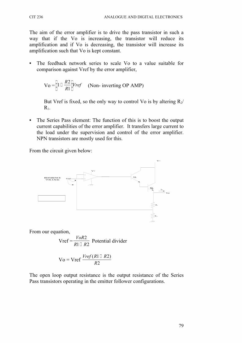
CIT 236 ANALOGUE AND DIGITAL ELECTRONICS
The aim of the error amplifier is to drive the pass transistor in such a way that if the Vo is increasing, the transistor will reduce its amplification and if Vo is decreasing, the transistor will increase its amplification such that Vo is kept constant.
• The feedback network series to scale Vo to a value suitable for comparison against Vref by the error amplifier,
Vo = VrefRR
+
121 (Non- inverting OP AMP)
But Vref is fixed, so the only way to control Vo is by altering R2/R1.
• The Series Pass element: The function of this is to boost the output current capabilities of the error amplifier. It transfers large current to the load under the supervision and control of the error amplifier. NPN transistors are mostly used for this.
From the circuit given below:
Vo
Q1
Q2
R2
R1
-
+
V+
V+
IO
REFERENCE VOLTAGE
Vref
From our equation,
Vref =21
2RR
VoR+
Potential divider
Vo = Vref 2
)21(R
RRVref +
The open loop output resistance is the output resistance of the Series Pass transistors operating in the emitter follower configurations.
79

CIT 236 ANALOGUE AND DIGITAL ELECTRONICS
From the circuit diagram,
The NPN BJT generates a collector circuit β times as large as that entering the base terminal. Ic = βIB
And releases both Ic and IB to the Emitter.IE = Ic + IB , therefore IE = (β + 1)IB
For low Power BJTs, VBE (ON) ~ 0.7 and β ~ 100 or more but
For Power Transistors, VBE (ON) ~ 1V and β is in the range of 10s.For this reason, Darlington pairs are used to give β of the range of 1000s or more.
Example 1
From the circuit below:
(a) Determine the voltage and current at the OP AMP output (b) Find the minimum value of Vi at which the circuit will still
function properly.
Vi
Vo = 5V
Q1
Q2
10K
10K
LOAD
+
-
Vref
33K
2.5V
Vn
R4
510Ω
3.3K R5
IR5
IR2
IE2
IL
RL = 1Ω
VBE1 = 0.8 VBE2 = 1V
β1 = 75 β2 = 15
Solution
a. VoA = OP AMP output voltageIoA = OP AMP output current.
From Kirchoff’s law,
80

CIT 236 ANALOGUE AND DIGITAL ELECTRONICS
IE2 + IR5 – IL – IR2 = 0
Therefore, IE2 = IL + IR2 – IR5
Since Vo = 5V and RL = 1Ω, IL = 5ATherefore, IL = 5A, IE2 = (β2 + 1) Iβ2
Therefore, Iβ2 =
+ 12
2
βEI
But IE2 ~ IL, therefore Iβ2 =
+ 1155
= 312.5mA
IE1 = Iβ2 + IR5 = 312 + IR5
IR5 =
5
2
RVBE
IE1 = 312.5mAIβ1 = ( IE1 ) = 312.5mA = 4.1mA
β1 + 1 76VR4 = Iβ1R4 = (4.1mA)(510) = 0.0041A (510)=2.1V
Therefore, the output voltage of the opamp is
VOA = 5V + VBE2 + VBE1 + VR4
= 5V + 1 + 0.8 + 2.1 = 8.9V
The output current of the opamp is the same as IB1, IOA = Iβ1 = 4.1mA
b. For the circuit to work properly the opamp must be within the linear region and the Vi must be at least 2 Volts greater than VoA. Therefore Vi ≥ 11V.
3.4 Protection Circuits
The performance of power transistors is affected by a number of factors such as Power dissipation capabilities, maximum voltage and current rating, maximum junction temperature; etc. This factor restricts the operation of the transistor to an area on the V & I curves known as the Safe Operating Area (SOA).
The SOA is defined as the area on the V and I curve within which the device can be operated without the risk of failure or degradation. To ensure reliable operation, regulators are equipped with additional circuits which serves to limit the current or switch off the transistors
81

CIT 236 ANALOGUE AND DIGITAL ELECTRONICS
should they be pushed outside the SOA. These circuits are inactive under normal operating conditions and get activated as soon as the SOA boundary is approached.
Examples of these circuits are:
1. Overload Protection
The purpose of this circuit is to prevent the current through the series pass transistor from exceeding a predetermined value. This is also known as short circuit protection.
Vi
Vo = 5V
Q1
LOAD
+
-
33K
2.5V
R4
R4
R2
R1
Rsc
Q2
OVERLOAD PROTECTION
The protection circuit alone is shown below
Q2
IOA IB1
Vi
IE1
Rsc
IO
VO
IE2
IC2
IB2
82

CIT 236 ANALOGUE AND DIGITAL ELECTRONICS
A single transistor Q2 and RSC is used to implement the circuit. The function of RSC is to sense IE1 (Io) and develop a voltage drop of sufficient magnitude to switch on Q2 when Io reaches the preset value.
RSC = maxmax1
)(2 7.0
OE
onBE
IIV
=
Under normal conditions, Io ≤ IE1max and the voltage is insufficient to switch on Q2.But when Io = IE1max = Iomax,the voltage across RSC is such that Q2 is turned on (Vbe is attained). Then current in excess of IB1max is diverted to Q2 as IC2.
Example
Vi
Vo = 5V
Q1
LOAD
+
-
33K
2.5V
510Ω
10K
10K
Rsc
Q2
IRsc
IL
IE2
In the circuit above,
βi = 75, VBE1 = 0.8V, β2 = 150, VBE2 = 0.7V, RSC = 2.2Ω, Vi = 12VFor the overload protection,
RSC = 0.7 I(RSC)
IRSC = 0.7 = 0.318 = 0.32A 2.2
The maximum current as set by the overload protection is 320mA.
a. With RL = 25Ω, the actual load current becomes – IL = VL = Vo = 5 = 0.2 = 200mA. IC1 = 200mA, IC2 = 0mA
83
CIT 236 ANALOGUE AND DIGITAL ELECTRONICS
RL RL 25VRSC = ILRSC = 2.2 x 0.2 = 0.44V.
The voltage drop across RSC = 0.44V but a value of 0.7V is needed to switch Q2 on. So with 0.44V,Q2 is off and the protection circuit is in active.
b. With RL = 10Ω,IL = Vo = 5 = 0.5 = 500mA
RL 10VRSC = ILRSC = 0.5 x 2.2 = 1.1V
The voltage across RSC = 1.1V so the transistor Q2 is switched on.
But IL(max) = 320mA, therefore VRL = 0.32 * 10Ω = 3.2V. Vo = 3.2VB1 = VRL + VBE1 + VBE2
VB1 = 3.2 + 0.7 + 0.8 = 4.7V.
But Vn = VoR1 = 3.2 (10K) Since Vo = ILmaxVL = 3.2V R1 + R2 20KVn = 1.6V, Vp = 2.5V
Maximum output swing of the opamp is 2 volts less than Vi
Therefore Vo = 12 – 2 = 10V.I(output current of opamp) = ( VOA – VB1 ) = 10 – 4.7
R4 510IOA = 10.4mABut IB1 = IC1
β
Therefore IB1(max) = βIC1max , IE1max = IL(max)
IB1(max) = (75 +1)IB1(max) = IE1max = 320mA = 4.2mA
(β+1) 76
The balance of IOA is absorbed by Q2.
Therefore IC2 = IOA – IB1max = 10.4 – 4.2 IC2 = 6.2mA, IB2 = IC2 = 0.04mA
β2
IB2 + IC2 = IE2 ~ 6.2mA
The final current delivered to the load is given by
IL = IRSC + IE2 …………………………….Kirchoff’s current law.
IL = 320 + 6.2 = 326.2mA.
84

CIT 236 ANALOGUE AND DIGITAL ELECTRONICS
2. SOA Protection
To restrict the BJT within the SOA,Ic must be reduced as VCE rises above a safe level. This protection is used in circuits with a high possibility of transients or spikes in the unregulated input.
Vi
Vo (5V)
Q1
LOAD
+
-
R3
2.5V
R4
Rsc
Q2
R5
R6
D2
For values of Vi insufficient to turn on D2 the protection remains inactive. From the zener diode characteristic curve below, when the voltage difference between Vi and Vo is beyond VZ2, the zener diode begins to conduct. This forces Q2 to also conduct because IZ2 will supply IB2 and when Q2 begins to conduct, IB1 is reduced and the current output of the circuit is limited. This circuit is achieved by R6, R5, D2. R6 limits the current through D2 and R5 decouples Q2 base from the Low Impedance point at Q1’s emitter.
3 Thermal Shut down
This form of protection which is mostly used in high power regulators due to possibility of damage due to self heating is implemented by sensing the elements junction temperature and reducing the power dissipation until the temperature drops to a tolerable level. The circuit is shown below:
85

CIT 236 ANALOGUE AND DIGITAL ELECTRONICS
Vi
Q1
LOAD
+
-
R3
R4
Q2
Q3
R7
R8
As temperature increases, the value of VBE3 reduces to a value set by R7
& R8 and Q3 starts conducting.The protection is achieved by using Q3, R7 and R8.The basis for this operation is that Vbe of a diode varies with temperature.
δVBE3 = -2mV/oC δT
At 25oC, VBE3 ~ 700mV.
As temperature increases to 175oC, the value of VBE3 = 700mV – (175 – 25)(2)= 400mV.
This value is provided by the R7 and R8.When Q3 is switched on, it reduces the IB1 which in turn reduces the output current. For fast response, Q3 is usually glued to Q1 to provide excellent thermal coupling.
The three forms of protection can be implemented in one circuit diagram as shown below
86

CIT 236 ANALOGUE AND DIGITAL ELECTRONICS
Vi
Q1
LOAD
+
-
R3
R4
Q2
Q3
R7
R82.5V
5.1K
2.1K
0.4K
510Ω
R2 10K
10KR1
R6
R5
3.5 Integration Circuit Regulators
There are different types of IC voltage regulators. Some of these include:
(1) Three terminal Fixed Voltage Regulators e.g. μa7800 series (+), μA7900 series (-)
(2) There terminal adjustable Regulators e.g. LM 317 (+), LM 337 (-)
(3) Four terminal adjustable Regulators μA78G(4) Dual Tracking Regulators(5) Low Dropout Voltage Regulators.
1. Three Terminal Fixed Voltage Regulators
These regulators come with 3 pins, one each for unregulated input, regulated output and ground. They are produced to specific voltage values. Examples of these include the LM 78XX series for positive voltage and the LM 79XX for the negative voltage. The last two digits specify the output voltage of the chip.
LM 7805 LM 7905LM 7806 LM 7906LM 7812 LM 7912LM 7815 LM 7915LM 7824 LM 7924
87

CIT 236 ANALOGUE AND DIGITAL ELECTRONICS
The low power versions are available in plastic or metal packages like small transistors while high power versions are packaged in TO-3 type metal cans or TO 220 type moulded plastic packages.
COMMON 3
OUTPUT
INPUT
20
10
T0 – 3 PACKAGE
OUTPUT
COMMON
INPUT
To 220 PACKAGE
The device will generate the specified output provided. The input is greater than the required output by 2.5V.This value is known as the drop out voltage and provided the output voltage is not exceeded.
UNREGULATED VOLTAGE7.5 – 35V
78051 2
3
C1 0.33 0.1uFC2
REGULATED OUTPUT
5V,1A
The data sheets recommend the use of two capacitors, C1 which alters out the effect of stray inductance in the input wires and C2 which improves the transient response to sudden load current changes.
Other examples are the LM 340 (Positive regulator) and the LM 320 negative regulator; etc.
2 Three Terminal Adjustable Regulators
These types of regulators rely on external resistors to set the output voltage. Products in this category include the LM 317 (Positive) and the LM 337 (negative) regulators.
88

CIT 236 ANALOGUE AND DIGITAL ELECTRONICS
IN OUT
Adj
Vi
R1
R2
Vo
The common terminal is floated and now used as the adjustment pin.The functional diagram of the LM 317 is shown below.
-
+
1.25V
A dj
50µA
Input
IQ
IQ PRO TECTION C IRCUIT
OPamp
0.2Ω
500
Output
Once the circuit is powered, the error amp drives Vo to whatever value is needed to make Vn = Vp.
Therefore Vo = VADJ + 1.25V
The purpose of R1 and R2 is the setting of the value of Vo.
From a given formula (from data sheets)
Vo = ( 1 + ) ( 1+ ) 1.25V
Current through R1 is given to be 5mA.
Therefore, the equation above simplifies to
Vo = ( 1 + ) 1.25
89

CIT 236 ANALOGUE AND DIGITAL ELECTRONICS
By varying R2 , Vo can be adjusted to any value in the range of 1.25 ≤ Vo ≤ 35V.
The lower limits correspond to R2 = 0, (i.e. Adj is grounded.)
11.0 CONCLUSION
In this unit you have been introduced to the basic principles of the DC power amplifier, its applications and the design procedure.
12.0 SUMMARY
In this unit we have been able to extend knowledge of the theory and applications of the Dc power supply and have been able to derive the different parameters of the DC power supply circuit.
13.0 TUTOR-MARKED ASSIGNMENT
From the circuit below:
(1) Determine the voltage and current at the OP AMP output(2) Find the minimum value of Vi at which the circuit will still
function properly.
Vi
Vo = 5V
Q1
Q2
10K
10K
LOAD
+
-
Vref
33K
2.5V
Vn
R4
510Ω
3.3K R5
IR5
IR2
IE2
IL
RL = 2Ω
VBE1 = 0.8 VBE2 = 1V
β1 = 75 β2 = 15
90

CIT 236 ANALOGUE AND DIGITAL ELECTRONICS
14.0 REFERENCES/FURTHER READINGS
Fitchen F.C; (1972). Transistor Circuit Analysis and Design. Second Edition Van Nostrand Reinhold Publishers.
Maddock R.J and Calcutt D.M (1994). Electronics: a Course for Engineers Second Edition. Longman Publishers.
Neamen D.A (1996). Electronics Circuit Analysis and Design. McGraw-Hill Publishers.
91

CIT 236 ANALOGUE AND DIGITAL ELECTRONICS
UNIT 3 HEAT SINKS
CONTENTS
1.0 Introduction2.0 Objectives3.0 Main Content
3.1 Heat Sink3.2 Thermal Resistance3.3 Free Air Operation3.4 Heat Sink Operation
4.0 Conclusion5.0 Summary6.0 Tutor-Marked Assignment7.0 References/Further Readings
1.0 INTRODUCTION
A heat sink is a metallic material attached to an integrated circuit chip or a high power dissipating transistor. Its aim is to increase the total surface area of the component thereby increasing the rate of heat dissipation of the component .Its purpose is to ultimately prolong the life of the component.
2.0OBJECTIVES
At the end of this unit, student should be able to:
• identify heat sinks • analyze the Heat sink design • design heat sinks for amplifier circuits.
3.0 MAIN CONTENT
3.1 Heat Sinks
The heat dissipated in Integrated circuits and other electronic circuits must be removed or the circuits will be damaged due to excessive temperature rise. Devices based on P-N junction like transistors, diodes, Integrated circuits are the most affected as all the heat is produced at the P-N junction. The power dissipated in the transistor increases its temperature above the ambient temperature. If the device or junction temperature Tj becomes too high, the transistor may suffer permanent damage.
92

CIT 236 ANALOGUE AND DIGITAL ELECTRONICS
The maximum allowable chip temperature referred to as the maximum junction temperature is given in data sheets. For silicon devices, this is usually in the range of 1500C TO 2000C.
To prevent excessive junction temperature build up, heat must be expelled from the silicon chip to the surrounding package structure and then to the ambient. Heat transfer is directly proportional to surface area so the larger the surface area of the chip, the faster the heat transfer from the chip. But design specifications place limits on the chip area, so an approach at increasing the surface area of chips is through the use of heat sinks.
A heat sink is a metal structure usually with fins that is bonded, clipped or clamped to the device package to facilitate heat flow from case to ambient.
3.2 Thermal Resistance
As the chip’s temperature increase with respect to the ambient, at thermal equilibrium this increase is proportional to the internally dissipated power.
TJ – TA ~ θJA PD.
where TJ and TA are junction and ambient temperatures respectively. PD is the dissipated power and θJA is the junction to ambient thermal resistance in oC/W.
The rate of loss of heat is proportional to the temperature difference between the junction and the ambient (case).
θ=
The thermal resistance and maximum allowable junction temperature set an upper limit on the power dissipation capabilities of devices such as power amplifiers, voltage regulators e.t.c no heat sink is used, the device will be said to be operating in free air.
3.3 Free Air Operation
In free air operation, the thermal resistance consists of two components,θJA = θJC + θCA
θJC = thermal resistance from junction to case
93

CIT 236 ANALOGUE AND DIGITAL ELECTRONICS
θCA = thermal resistance from core to ambient
This can be illustrated in the diagram below:
PD
θjc
θCA
TA
Tj
TC
The values for θJC and θJA are usually provided but θCA must be calculated.
3.4Heat Sink Operation
When a heat sink is used, the equation gets modified
TJ – TA = PDθJA
Where θJA = (θJC + θCS + θSA)
θJC = thermal resistance between junction and case
θCS = thermal resistance between case and heat sink
θSA = thermal resistance between heat sink and ambient.
Therefore, TJ – TA = PD (θJC + θCS + θSA)
Where PD = Power dissipated in the device.The presence of the heat sink alters the thermal resistance between case and ambient.
θCA =θCS + θSA
The Electrical diagram for this is shown below
94

CIT 236 ANALOGUE AND DIGITAL ELECTRONICS
PD
θjc
θCS
TA
Tj
TC
θSA
Tsink
Example 1
Determine the maximum power dissipation in a MOSFET with the following parameters:
θJC = 1.75OC/ W , θCS = 1OC/ W, θSA = 5OC/ W, θCA = 50OC/ W, TA = 30OC and Tjmax = 150OC.
Without Heat Sink
TJ – TA = PD (θJC + θCA)150 – 30 = PD (1.75 + 50)Therefore, PD = = 2.32W
With Heat Sink
TJ – TA = PD (θJC + θCS + θSA) = 150-130=PD (175+1+5)PD = = = 15.5W
From the example, the heat sink allows power to be dissipated in the device while keeping the temperature below TJ.
Example 2
A given transistor has θJA = 200OC/ W, TA = 30OC.
Power dissipation of 100mW will give a Tj of PD = 100mW = 0.1W
Δ Tj = PDθJA = 200 * 0.1 = 20OC.
The new junction temperature Tj = TA + Δ Tj
Therefore Tj = 30oC + 20oC = 50oC.
95

CIT 236 ANALOGUE AND DIGITAL ELECTRONICS
The thermal contact between the case and the heat sink must be of low thermal resistance and a thermally conducting paste should be used to bond the heat sink to the case.
Heat sinks are made in many shapes and sizes. They are often painted in black to aid radiative heat transfer. Cooling fans are also used if the heat sink gets too hot, this is called forced convection. Fans improve the dissipation of a heat sink by a factor of two or three and this leads to smaller heat sink design. Aluminium due to its light weight and low resistivity is often used in heat sink construction.
4.0 CONCLUSION
In this unit you have been introduced to the basic principles of the Heat sinks, its applications and the design procedure.
5.0 SUMMARY
In this unit we have been able to extend knowledge of the theory and applications of the heat sink and have been able to derive the design procedure for each application of the heat sink.
6.0 TUTOR-MARKED ASSIGNMENT
(1) 5V regulator is to satisfy the following requirements:
0oC≤TA≤60OC, IO(max) = 0.8A, Vi(max) = 12V, TJmax = 125OC.
Select a suitable heat sink for it.
(2) A silicon transistor has θJC = 10OC/ W and θCA = 30OC/ W.
(a)Determine PDMAX of TA = 30OC and TJ = 150OC.(b) When a heat sink of θHA = 7OC/ W is used, determine the TJ of
PD = 5W
7.0 REFERENCES/FURTHER READINGS
Fitchen F.C; (1972). Transistor Circuit Analysis and Design. Second Edition Van Nostrand Reinhold Publishers.
Maddock R.J and Calcutt D.M (1994). Electronics: a Course for Engineers Second Edition. Longman Publishers.
Neamen D.A (1996). Electronics Circuit Analysis and Design. McGraw-Hill Publishers.
96

CIT 236 ANALOGUE AND DIGITAL ELECTRONICS
MODULE 4
Unit 1 Boolean AlgebraUnit 2 Logic GatesUnit 3 Karnaugh Map
UNIT 1 BOOLEAN ALGEBRA
CONTENTS
1.0 Introduction2.0 Objectives3.0 Main Content
3.1 Boolean Algebra3.2 DeMorgan’s Theorem
4.0 Conclusion5.0 Summary6.0 Tutor-Marked Assignment7.0 References/Further Readings
1.0 INTRODUCTION
The objective of this course is to introduce the student to the field of digital systems. Starting at the fundamental level of Boolean algebra and the different laws used in the resolution of digital electronics circuits.
2.0 OBJECTIVES
At the end of this unit, students should be able to:
• the understanding of Boolean algebra and its laws• the introduction of the Boolean algebraic identities• the introduction of the De Morgan’s theorem.
3.0 MAIN CONTENT
3.1 Boolean Algebra
Boolean algebra is the basic mathematics for the study of logic design .Basic laws of Boolean algebra are implemented as switching devices called logic gates. A Boolean variable can take on two values ‘0’ and ‘1’, ‘T’, ‘F or H,L or ON,OFF . Boolean operations transform Boolean Variables the basic operations are NOT, AND, OR
97

CIT 236 ANALOGUE AND DIGITAL ELECTRONICS
More complicated Boolean Functions can be derived from the basic Boolean operations.
Basic Boolean algebraic identities
A + 0 = AA + 1 = 1A + A = AA + A = 10*A = 01*A = AA*A = AA*A = 0
AA =
Laws of Boolean algebra
Commutative Law
(a) A + B = B + A(b) A B = B A
Associate Law
(a) (A + B) + C = A + (B + C) (b) (A B) C = A (B C)
Distributive Law
(a) A (B + C) = A B + A C(b) A + (B C) = (A + B) (A + C)
Identity Law
(a) A + A = A (b) A A = A
Redundance Law
(a) A + A B = A (b) A (A + B) = A
Other Boolean Identities
(a) (b)
98
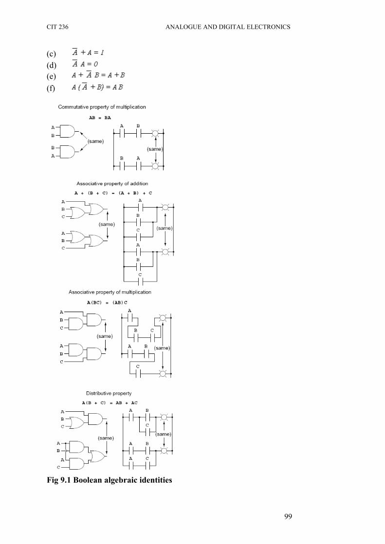
CIT 236 ANALOGUE AND DIGITAL ELECTRONICS
(c) (d) (e) (f)
Fig 9.1 Boolean algebraic identities
99

CIT 236 ANALOGUE AND DIGITAL ELECTRONICS
Example 1
Prove (a) BABAA +=+
Solution
(1) Algebraically:
BAAABA
BAABA
BABA
BAABAA
+=++=
++=
++=
+=+
)(
)1(
1
(2) Using the truth table:
Table 9.1: Truth table for the example 9.1A B A+B BA A+ BA
0 0 0 0 0
0 1 1 1 1
1 0 1 0 1
1 1 1 0 1
3.2 DeMorgan’s Theorem
DeMorgan’s Theorem allows gates to be converted to others by simply inverting the inputs of the selected gate. More specifically, you can convert gates to others if the following steps are followed accordingly:
1. Complement all inputs.2. Convert all AND operations to ORs3. Convert all OR operations to ANDs4. Complement the entire expression.
BABA
BABA
•=+
+=•
The key to the theorem is break the line, change the sign
100

CIT 236 ANALOGUE AND DIGITAL ELECTRONICS
The truth table to prove the theorem is shown below.A B A B BA + BA • BA • BA +
0 0 1 1 1 1 1 1
0 1 1 0 0 0 1 1
1 0 0 1 0 0 1 1
1 1 0 0 0 0 0 0
4.0 CONCLUSION
In this unit you have been introduced to the basic principles of the Boolean algebra and the demorgans theorem.
5.0 SUMMARY
In this unit we have been able to extend knowledge of the theory and applications of Boolean algebra, the De Morgan’s theorem and the different rule that govern the use of Boolean algebra in digital electronics.
6.0 TUTOR-MARKED ASSIGNMENT
(1) Simplify the expression using Boolean algebra
yxxyyx ++ zyxzxxyx +++
C B ABDC BA ])([ ++ABCC BAC B AC BABCA ++++
(2) Apply DeMorgan’s theorems to the following expression)( FED CBA +++ .
7.0 REFERENCES/FURTHER READINGS
Fitchen F.C; (1972). Transistor Circuit Analysis and Design. Second Edition Van Nostrand Reinhold Publishers.
Maddock R.J and Calcutt D.M (1994). Electronics: a Course for Engineers Second Edition. Longman Publishers.
Neamen D.A (1996). Electronics Circuit Analysis and Design. McGraw-Hill Publishers.
101

CIT 236 ANALOGUE AND DIGITAL ELECTRONICS
UNIT 2 LOGIC GATES
CONTENTS
1.0 Introduction2.0 Objectives3.0 Main Content
3.1 Logic Gates3.2 OR Gate3.3 AND Gate3.4 NOT Gate3.5 NOR Gate3.6 NAND Gate3.7 XOR Gate3.8 XNOR Gate
4.0 Conclusion5.0 Summary6.0 Tutor-Marked Assignment7.0 References/Further Readings
15.0 INTRODUCTION
A logic gate is an electronic circuit which makes logic decisions. It has one output and one or more inputs. They are the fundamental blocks with which digital systems are built. The output is a result of the implementation of the logical algebra known as the Boolean algebra.
16.0 OBJECTIVES
At the end of this unit, student should be able to:
• identify the different logic gates• analyze circuits with logic gates• generate other gates from the universal gates.
17.0 MAIN CONTENT
3.1 Logic Gate
One characteristic of this Boolean algebra is that the variables can only assume one of the two values 0 and 1. Where 0 (zero) can represent off, low, minus or false depending on the convention used while 1 (one) takes the opposite state. The gates are available in various IC families, popular among them are the transistor- transistor logic (TTL), emitter coupled logic (ECL), metal oxide semiconductor (MOS) and the complementary metal oxide semiconductor (CMOS). Most of these
102

CIT 236 ANALOGUE AND DIGITAL ELECTRONICS
families have their unique characteristics and qualities for example, the TTL families consume considerable quiescent current while the CMOS which is factor than the TTL consumes zero quiescent current (though it is more delicate) among other properties.
We shall be considering the following gates and their truth table OR gate, AND gate, NOT gate, NOR and NAND gates. Another gate we will look at is the exclusive OR gate. The logic used to determine the state of the variables can either be positive or negative. In the positive logic, where there are two voltage values, the more positive of the voltage represents the high while if we are operating on the negative logic, the more negative value would represent the high state.
3.2 OR Gate
The OR gate is a gate which produces a high output of any or both (all) if its inputs are high. It symbolizes logic addition.
Figure 2 input OR gate
From the diagram (b) we see that so long as any of the switches is closed the bulb will light up. The OR gate represents the Boolean equation;
A B C0 0 00 1 11 0 11 1 1
103

CIT 236 ANALOGUE AND DIGITAL ELECTRONICS
NOTE: a truth table is a table which gives the output state for all the possible input combination.
This OR gate can also be known as an inclusive OR gate because it includes the case when both input are true. Gates can have any number of inputs but standard packages contain four 2- input gates, three 3- input gates. The OR gate can also be derived from discrete circuits. e.g. diodes and transistors.
3.3 AND Gate
The AND gate is a logic gate which will give a high output if and only if all its inputs are high. It symbolizes logical multiplication.
SYMBOL
Figure 2 –input AND gate
The AND gate works on the Boolean algebra
From the diagram it can be seen that an AND gate can be represented by a series circuit. For the lamp to come on, the switches A and B must be on. Below are truth tables for two and three input AND gates.
104

CIT 236 ANALOGUE AND DIGITAL ELECTRONICS
Two input AND gate. C = output Three input AND gate. D = output
The AND gate can also be realized using the diode and the transistor.
3.6 The NOT Gate (Inverse)
The NOT gate is also known as an inverter because it inverts the input signal. It has one input and one output terminal. The logical symbol for negation or inversion is a bar over whose function is to indicate the opposite state. The symbol of the NOT gate is shown below. Truth table for the NOT gate
A B
0 1
1 0
Figure NOT gate symbol
NAND/NOR GATES
The gates (AND/OR) discussed above can be combined with the NOT gate to produce other gates known as the NOR and the NAND gates. This is achieved by inverting the inputs of the gates.
3.7 The NOR Gate
The NOR gate is a combination of the NOT and the OR gate. The NOT gate function is a reverse of the OR gate function so it will have an output of 1 only when all its inputs are 0. The output of the NOR gate is fed to the input of the NOT gate to give NOR.
The NOR gate is also referred to as a universal gate because it can be used to simulate OR, AND and NOT gate functions. The NOR gate
A B C
0
0 0
0 1 0
1 0 0
1 1 1
A B C D
0 0 0 0
0 0 1 0
0 1 0 0
0 1 1 0
105
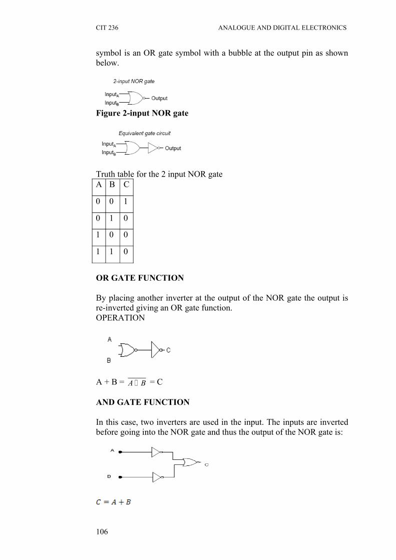
CIT 236 ANALOGUE AND DIGITAL ELECTRONICS
symbol is an OR gate symbol with a bubble at the output pin as shown below.
Figure 2-input NOR gate
Truth table for the 2 input NOR gateA B C
0 0 1
0 1 0
1 0 0
1 1 0
OR GATE FUNCTION
By placing another inverter at the output of the NOR gate the output is re-inverted giving an OR gate function.OPERATION
A + B = BA + = C
AND GATE FUNCTION
In this case, two inverters are used in the input. The inputs are inverted before going into the NOR gate and thus the output of the NOR gate is:
106

CIT 236 ANALOGUE AND DIGITAL ELECTRONICS
NOT GATE FUNCTION
In this case the two inputs are tired together and the output is A + A which by demorgan is A. the OR and AND gates can also be derived from using purely NOR gates.
3.8 NAND Gate
In this case the circuit of the AND gate is fed to the input of an inverter. The gate gives an output of 1 if either A or B or both are 0. The NAND gate is also a universal gate as it can be construed as shown to get either an AND gate or an OR gate operation. The NAND gate symbol is an AND gate symbol with a bubble at the output pin as shown below.
A B C0 0 10 1 01 0 11 1 0
Implementation of a NOT gate using a NAND
Implementation of an AND gate using a NAND
Implementation of an OR gate using a NAND
3.9 XOR Gate
107

CIT 236 ANALOGUE AND DIGITAL ELECTRONICS
Exclusive-OR gates output a high, (1) logic level if the inputs are at different logic levels, either 0 and 1 or 1 and 0. Conversely, they output a low (0) logic level if the inputs are at the same logic levels. The Exclusive-OR (sometimes called XOR) gate has both a symbol and a truth table pattern shown below:
There are equivalent circuits for an Exclusive-OR gate made up of AND, OR, and NOT gates, just as there were for NAND and NOR gates. A rather direct approach to simulating an Exclusive-OR gate is to start with a regular OR gate, then add additional gates to inhibit the output from going, high, (1) when both inputs are high. (1):
3.10 XNOR Gate
Exclusive-NOR gate, otherwise known as the XNOR is equivalent to an Exclusive-OR gate but it has an inverted output. The truth table for this gate is exactly opposite as for the Exclusive-OR gate:
Example 1
A digital signal 101011 is applied to a NOT gate what will be the NOT gate output.
Input = 1 0 1 0 1 1
Output = 0 1 0 1 0 0
SELF ASSESSMENT EXERCISE
1. Two signals A = 1 0 1 1 0 1 and B = 1 1 0 1 0 1 are fed to a 2 input AND gate sketch the output signal.
108

CIT 236 ANALOGUE AND DIGITAL ELECTRONICS
2. Convert the following Boolean expression to logic using different logic gates.(A. B + C)
18.0 CONCLUSION
In this unit you have been introduced to the different logic gates, their symbols and applications.
19.0 SUMMARY
In this unit we have been able to extend knowledge of the theory and applications of the different types of logic gates.
20.0 TUTOR-MARKED ASSIGNMENT
1) Two signals A = 1 0 1 1 0 1 and B = 1 1 0 1 0 1 are fed to a 2 input AND gate sketch the output signal.
2) Using DeMorgan’s theorem, convert the following Boolean expressions to equivalent expressions that (i) have only OR and complement operations, and show that the functions can be implemented with NOR gates only; (ii) have only AND and complement operations, and show that the functions can be implemented with NAND gates only.
(a) zyzxyx f ++= (b) ))()(( zyyxzy f +++=
3) Express the switching circuit shown in the figure in binary logic notation and generate the truth table
21.0 REFERENCES/FURTHER READINGS
Fitchen F.C; (1972). Transistor Circuit Analysis and Design. Second Edition Van Nostrand Reinhold Publishers.
Maddock R.J and Calcutt D.M (1994). Electronics: a Course for Engineers Second Edition. Longman Publishers.
109

CIT 236 ANALOGUE AND DIGITAL ELECTRONICS
Neamen D.A (1996). Electronics Circuit Analysis and Design. McGraw-Hill Publishers.
110

CIT 236 ANALOGUE AND DIGITAL ELECTRONICS
UNIT 3 KARNAUGH MAP
CONTENTS
1.0 Introduction2.0 Objectives3.0 Main Content
3.1 Introduction to Karnaugh Maps3.2 Circuit Simplification Using Karnaugh Maps3.3 Simplifying Logic Circuits Using Karnaugh Maps
4.0 Conclusion5.0 Summary6.0 Tutor-Marked Assignment7.0 References/Further Readings
1.0 INTRODUCTION
In the design of logic functions by means of logic gates, more than one solution is usually available for the implementation of a given logic expression and some combinations of gates can implement a given function more efficiently than others. The challenge in logic design is the assurance of having chosen the most efficient realization.
A very popular and easy to use procedure for simplifying logic design exists and it utilizes a map, describing all possible combinations of the variables present in the logic function of interest. This map is called a Karnaugh map, after its inventor. The karnaugh map consists of row and column assignments for two or more variables arranged so that all adjacent terms change by only one bit. Each map consists of 2N cells, where N is the number of logic variables. Karnaugh maps allow us to convert a truth table to a simplified Boolean expression without using Boolean Algebra.
4.0OBJECTIVES
At the end of this unit, student should be able to:
• the understanding of the use of karnaugh maps in logic design• the understanding of the use of karnaugh maps in simplification of
logic design• the understanding of conversion of truth tables to Boolean algebra • the generation of digital logic circuits from truth tables.
3.0 MAIN CONTENT
111

CIT 236 ANALOGUE AND DIGITAL ELECTRONICS
3.1 Introduction to Karnaugh Maps
Karnaugh maps are a graphical way of simplifying a Boolean expression and thus simplifying the resulting circuit. A Karnaugh map is a completely mechanical method of performing this simplification, and so has an advantage over manipulation of expressions using Boolean algebra. Karnaugh maps are effective for expressions of up to about six variables. For more complex expressions the more advanced Quine-McKluskey method may be appropriate.
The Karnaugh map uses a rectangle divided into rows and columns in such a way that any product term in the expression to be simplified can be represented as the intersection of a row and a column. The rows and columns are labeled with each term in the expression and its complement. The labels must be arranged so that each horizontal or vertical move changes the state of one and only one variable. The figure 9.1 below shows karnaugh map with 2,3and 4 variables
Figure 9.1 Karnaugh maps with 2, 3, 4 variables
3.2 Circuit Simplification Using Karnaugh Maps
112

CIT 236 ANALOGUE AND DIGITAL ELECTRONICS
The following steps are required to use a Karnaugh map to simplify an expression:
1. Draw a “map” with one box for each possible product term in the expression.The boxes must be arranged so that a one-box movement either horizontal or vertical changes one and only one variable. See Figure 9.1.
2. For each product term in the expression to be simplified, place a checkmark (or a 1) in the box whose labels are the product's variables and their complements.
3. Draw loops around adjacent pairs of checkmarks. Blocks are “adjacent” horizontally and vertically only, not diagonally. A block may be “in” more than one loop, and a single loop may span multiple rows, multiple columns, or both, so long as the number of checkmarks enclosed is a power of two.
4. For each loop, write an unduplicated list of the terms which appear; i.e. no matter how many times A appears, write down only one A.
5. If a term and its complement both appear in the list, e.g. both A and A , delete both from the list.
6. For each list, write the Boolean product of the remaining terms.7. Write the Boolean sum of the products from Step 5; this is the
simplified expression.
Example 1
Simplify the Boolean expression below using karnaugh maps AB+ A B .
Solution
This is an expression of two variables. A rectangle is drawn and divided so that there is a row or column for each variable and its complement. Next, we place checks in the boxes that represent each of the product terms of the expression.
Figure 9.2: Karnaugh map for example 1The first product term is AB, so a check is placed in the upper left block of the diagram, the conjunction of A and B.
113

CIT 236 ANALOGUE AND DIGITAL ELECTRONICS
The second is A B , so we place a check in the lower left block. Finally, we draw a loop around adjacent pairs of checks. The loop contains A, B, A, and B . We remove one A so that the list is unduplicated. The B and B “cancel,” leaving only A, which is the expected result: AB+ AB = A.
Example 2
Simplify A B + A B + BA using K-Maps
Solution
There are two variables, so the K-Map is the same as in Example 1. The solution will be derived using the following steps:Place a check in the A B area.Place a check in the A B area.Place a check in the BA area.
Draw loops around pairs of adjacent checks.
Figure 9.3: Karnaugh map for example 2
The Vertical loop contains A , B, BA, . Since A is duplicated, one of it is removed. B and its complement B both cancel out leaving only A .
From the horizontal loop we have A, B , BA, .The duplicate B is removed and the A cancels out with its complement.The Boolean sum of the manipulation is now A + B which is the answer.
3.3 Simplifying Logic Circuits Using Karnaugh Maps
The major advantage of Karnaugh maps is its ability to simplify logic design by simplifying the Boolean expression and/or truth table and eliminating unnecessary logic gates in a digital logic design.
Example 3
Given the truth table for a 3 input logic design:
114

CIT 236 ANALOGUE AND DIGITAL ELECTRONICS
(1) Generate the Boolean equation and sketch the logic circuit required to implement the truth table
(2) Simplify the logic design using K-maps and sketch the resultant logic circuit.
The output is the X column.
Table 9.2 Output of the 3 input logic circuit
A B C X0 0 0 10 0 1 00 1 0 00 1 1 11 0 0 01 0 1 01 1 0 01 1 1 1
Solution
(1) From the truth table, the circuit generates an output when X = 1.The product of the terms at which X = 1 is taken out and summed together. This sum is known as sum of products and it is the Boolean expression that generates the truth table.
Products terms are: CBA , BCA and ABC
Sum of products = CBA + BCA + ABC
The digital logic circuit based on the Boolean equation is given below. Note, the inputs are A, B and C and the complements are CBA The complements are generated by the use of inverters or NOT gates. ABC complements are fed into a 3 input AND gate while BCA is fed into another 3 input AND gate and ABC is fed into the third 3 input AND gate. The inputs of the three 3-input AND gates are fed together into a 3-input OR gate. The circuit diagram is shown below.
115

CIT 236 ANALOGUE AND DIGITAL ELECTRONICS
Figure 9.4: Digital logic circuit for example 3
(2) The truth table generates an expression with three product terms. A measure of the complexity of a digital logic circuit is the number of gate inputs. The circuit in
Figure 9.4 has 15 gate inputs. The Karnaugh map for the sum of products expression is shown in Figure 9.5 below.
Figure 9.5 Karnaugh map for example 3
In this Karnaugh map, the large loop surrounds A B C and BCA .It “wraps around” from the left edge of the map to the right edge. The A and A cancel, so these two terms simplify to BC. CBA is in a cell all by itself, and so contributes all three of its terms to the final expression.
The simplified expression is B C + CBA and the simplified circuit is shown in Figure 9.6. In the simplified circuit, one three-input AND gate was removed, a remaining AND gate was changed to two inputs, and the OR gate was changed to two inputs, resulting in a circuit with ten gate inputs.
Figure 9.6: Simplified Circuit in example 3
116

CIT 236 ANALOGUE AND DIGITAL ELECTRONICS
4.0 CONCLUSION
In this unit you have been introduced to the use of the karnaugh map in simplification of digital logic circuits. The following observations are to be noted in the generation of loops in the K-maps. For maximum simplification, the loops are to be made as big as possible with big loops being the preferred size. The restriction is that the loop must be rectangular and enclose a number of checkmarks that is a power of two. When a map is more than two rows deep, i.e. when it represents more than three variables, the top and bottom edges can be considered to be adjacent in the same way that the right and left edges are adjacent in the two-by-four maps above. If all checkmarks in a loop are enclosed within other loops as well, that loop can be ignored because all its terms are accounted for.
5.0 SUMMARY
In this unit we have been able to extend knowledge of the theory and applications of the Karnaugh Maps.
6.0 TUTOR-MARKED ASSIGNMENT
1 Given the following Karnaugh maps, determine their logic equation.
2) Given the truth table for a 3 input logic design,(a) Generate the Boolean equation and sketch the logic circuit
required to implement the truth table in Table 9.3(b) Simplify the logic design using K-maps and sketch the
resultant logic circuit.
117

CIT 236 ANALOGUE AND DIGITAL ELECTRONICS
The output is the X column.
Table 9.3 Output of the 3 input logic circuit
A B C X0 0 0 00 0 1 00 1 0 10 1 1 11 0 0 01 0 1 11 1 0 11 1 1 1
3 Use a Karnaugh map to simplify A B C + A CB + CBA .
7.0 REFERENCES/FURTHER READINGS
Mendelson, Elliott, (1970). Schaum's Outline of Theory and Problems of Boolean Algebra. McGraw- Hill
Maddock R.J and Calcutt D.M (1994). Electronics: a Course for Engineers Second Edition. Longman Publishers.
Neamen D.A (1996). Electronics Circuit Analysis and Design. McGraw-Hill Publishers.
118