nasa · submillimeter (terahertz) ... 10 times more sensitive than a pyroelectric detector; ... •...
TRANSCRIPT

NASA-CR-192"/'99
JPL Publicatio_ i
N93-22912
Unclas
4
(NASA-CR-I92799) CENTER FOR SPACE
M[CROELECTRONICS TECHNOLOGY
Technicil Report, 199I (JPL)
mm 105 p
G3/33 0154716
Center for Space Microelectronics Technology
1991 Technical Report
July1,1992 8L._K
ORIGINAL PAGE
AI'_D WHITE PHOTOG,_,_I-I
NASANational Aeronautics and
Space Administration
Jet Propulsion Laboratory
California Institute of Technology
Pasadena, California C S M T
https://ntrs.nasa.gov/search.jsp?R=19930013623 2018-06-27T07:36:05+00:00Z
Center for Space Microelectronics Technology
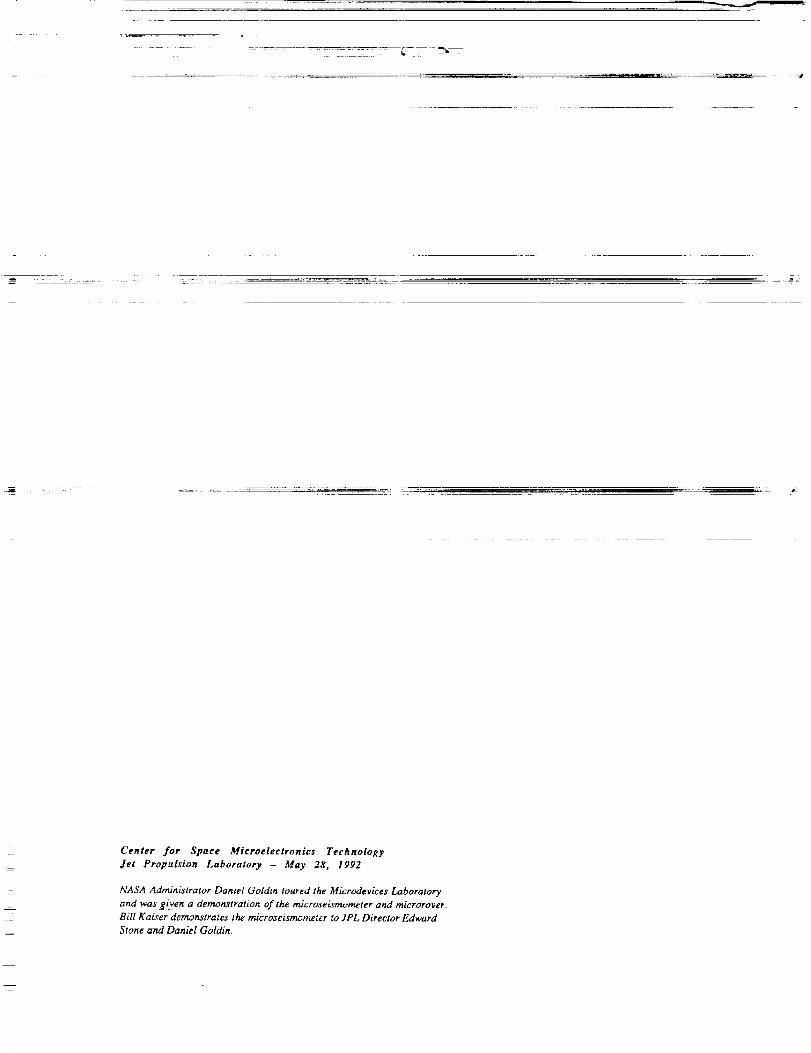
Jet Propulsion Laboratory - .¥1ay 28, 1992
NASA Administrator Daniel Goldin toured the Microdevices Laboratory
and was given a demonstration of the microseismometer and microrover.
Bill Kaiser demonstrates the microseismometer to JPL Director Edward
Stone and Daniel Goldin.

-.-- _. _. TECHNICAL REPORT STANDARD TITLE PAGE
1. Report No.JPL Pub .r92--131
2. Government Accession No.
4. Title and Subtitle
Center for Space Microelectronics
Technology 1991 Technical Report
3. Recipient's Catalog No.
5. Report DateJuly I, 1992
6. Performing Organization Code
L.
7. Author(s) Center for Space Microelectronics 8. Performing Organization Report No.
Technology
10. Work Unit No.9. Per_rming Organization Name and Address
JET PROPULSION LABORATORY
California Institute of Technology4800 Oak Grove Drive
Pasadena, California 91109
12. Sponsoring Agency Name and Address
NATIONAL AERONAUTICS AND SPACE ADMINISTRATION
Washingf0n, D.C. 20546
11. Contract or Grant No.NAS7-918
13. T_e of Report and Period Covered
Annual Technical Report
14. Sponsoring Agency Code
15. Supplementary Notes
16. Abstract
The 1991 Technical Report of the Jet Propulsion Laboratory Center
for Space Microelectronics Technology summarizes the technical
accomplishments, publications, presentations, and patents of the
Center during the past year. The report lists 193 publications,
211 presentations, and 125 new technology reports and patents.
17. Key Words (Selected by Author(s))
Neural Networks - Microcircuit
Technology - Computer Operationsand Hardware - Electronics and
Electrical Engineering - Solid
State Physics - IR, UV, Optical De
19. Security Cl_slf. _f this report)
Unclassified
18. DistributionStatement
Unclassified - Unlimited
:ect_on
_. Security Clmsif. _f thls page)
Unclassified
21. No. of Pages
108
22. Price
JPL. 0184 R 9183


JPL Publication 92-13
Center for Space Microelectronics
1991 Technical Report
Technology
July 1, 1992
I IASANational Aeronautics andSpace Administration
Jet Propulsion LaboratoryCalifornia Institute of TechnologyPasadena, California C S M T

The research described in this publication was carried out by the Jet Propulsion Laboratory,California Institute of Technology, and was sponsored by the National Aeronautics and
Space Administration; Strategic Defense Initiative Organization/Innovative Science andTechnology Office; Defense Advanced Research Projects Agency; U.S. Army; U.S. Navy;
U.S. Air Force; and U.S. Department of Energy.
Reference herein to any specific commercial product, process, or service by trade name,trademark, manufacturer, or otherwise, does not constitute or imply its endorsement by the
United State Government or the Jet Propulsion Laboratory, California Institute ofTechnology.
The report was prepared as an account of work sponsored by an agency of the UnitedStates Government. Neither the United States Government nor "any agency thereof, norany Of their employees, makes any warranty, lexpressed or implied, or assumes any legalliability or responsibility for the accuracy, completeness, or usefulness of any information,apparatus, product, or process disclosed, or represents that its use would not infringeprivately owned rights.
---- - 2 .... .
i

Abstract
The 1991 Technical Report of the Jet Propulsion Laboratory Center for SpaceMicroelectronics Technology summarizes the technical accomplishments, publications,
presentations, and patents of the Center during the past year. The report lists 193publications, 211 presentations, and 125 new technology reports and patents.
o,,
nl

Zzz
E_E
E
m
Table of Contents
Director's Report ................................................................................................................ 1
Technical Highlights ....................................................................................................... 3Programmatic Highlights ................................................................................................ 4Institutional Highlights ................................................................................................... 5
I. Solid State Devices ................................................................................................. 7
Overview ............................................ :............................................................................ 9
1991 Major Technical Achievements .............................................................................. 9Electron Tunneling .............................................................................................. 9Superconductivity ............................................................................................... 9Submillimeter (Terahertz) Receiver Technology ............................................... 10
Semiconducting Materials: Growth and Characterization ................................. 12Electronic Device Technology ........................................................................... 13Microinstrument Technology ............................................................................ 14Cultured Neuron Probe ..................................................................................... 14
Diamond Film Technology ............................................................................... 14Technical Progress Reports
Electron Tunneling ............................................................................................ 15
Superconductivity ............................................................................................. 19Submillimeter (Terahertz) Receiver Technology ............................................... 23Semiconducting Materials: Growth and Characterization ................................. 26Electronic Device Technology ........................................................................... 29Cultured Neuron Probe ..................................................................................... 33
Diamond Film Technology ................ ............................................................... 34
IL Photonics ................................................................................................................. 37
Overview ....................................................................................................................... 39
1991 Major Technical Achievements ............................................................................ 39
Spatial Light Modulators .................................................................................. 39Lasers ............................................................................................................... 39
Optoelectronic Materials and Characterization .................................................. 41Optoelectronic Integrated Circuits ..................................................................... 41Infrared Detectors ............................................................................................. 42
Nonlinear Optical Materials .............................................................................. 43Fiber Optics ...................................................................................................... 44Photovoltaic Technology ................................ ................................................... 44
Space Environmental Effects on Materials ........................................................ 45Technical Progress Reports
Spatial Light Modulators .................................................................................. 46Lasers ............................................................................................................... 48
Optoelectronic Materials and Characterization .................................................. 50Optoelectronic Integrated Circuits ..................................................................... 51Infrared Detectors ............................................................................................. 52
Nonlinear Optical Materials .............................................................................. 56Fiber Optics ...................................................................................................... 60
V PR_ P.alGE'.BLANK NOT FILMED

HI.
IWo
Wo
Photovoltaic Technology .................................................................................. 61Optical Signal Processing ................................................................................ 62Space Environmental Effects on Materials ....................................................... 63
Advanced Computing ......................................................................................... 65
Overview ...................................................................................................................... 67
1991 Major Technical Achievements ............................................................................ 67Parallel Computation ........................................................................................ 67Neural and Analog Computing ......................................................................... 68Neurocompufing Theory and Nonlinear Science .............................................. 69Optical Processing ........................................................................................... 71Data Storage ..................................................................................................... 72Software Engineering and Computer Science ................................................... 73
Technical Progress ReportsParallel Computation .... ............... '" ......... ,,,., ................. . ................................ 73Neural and Analog Computing ......................................................................... 78Neural and Nonlinear Theory ...... ,,. ............... 83Optical Processing ,., ................................. . .................................................... 87Data Storage ..................................................................................................... 89Software Engineering and Computer Science ................................................... 91
Custom Microcircuits ......................................................................................... 93
Overview ...................................................................................................................... 95
1991 Major Technical Achievements ............................................................................ 95Technical Progress Reports
Custom Microcircuits .... , ......... ......................................................................... 96
Appendix .................. .............................................................................................. 99
CSMT-Caltech Campus Collaborations ..................................................................... 101CSMT-Other Collaborations ...................................................................................... 103
Distinguished Visiting Scientists ................................................................................. 106Honors and Awards ................................................................................................... 107
Conferences and Workshops Sponsored and/or Hosted by CSMT ........................... 108
vi

Director's Report
This report is published on the fifth anniversary of the Center for Space MicroelectronicsTechnology (CSMT), which was founded in 1987 at Caltech's Jet Propulsion Laboratory(JPL). NASA and several Department of Defense (DoD) agencies with space responsibili-ties established CSMT in order to create a critical mass program in space microelectronics
with world-class facilities, equipment and staff.
The Center concentrates on innovative, high-risk, high-payoff concepts and devices with
the potential to enable future space missions and to significantly enhance current andplanned missions. CSMT conducts research and development in four technical areas:solid-state devices, photonics, custom microcircuits and advanced computing. Research
and development are pursued through proof of concept demonstration, and successesare transferred to engineering development at JPL, in other Government laboratoriesand industry.
CSMT focuses on those aspects of microelectronics and advanced computing that areunique to space applications. A concrete example is the development of new sensorsfor the very long wavelength infrared and submillimeter regions of the electromagneticspectrum where the atmosphere is opaque and one must get into space to do observations.Another example is the development of laser systems of specific wavelengths tuned to the
absorption lines of trace gases in the Earth's atmosphere.
Space systems require low mass and power consumption with extremely high reliability.CSMT's new thrust in microsensors and microinstruments directly addresses these issues.
Custom microcircuits, including electronic neural networks and low temperature sensorreadout chips, are major elements of the CSMT miniaturization program.
Analysis of the enormous amount of data generated by modem NASA and DoD spacemissions requires orders of magnitude increase in computing power, both on the spacecraftand on the ground, and similar improvements in communications rates. To support theserequirements, CSMT has aggressive programs in high performance parallel computing,data visualization, optical communications and gigabit networks.
After five years, CSMT has gained national recognition for its efforts in thefollowing areas:
Electron tunneling.
Terahertz/submillimeter technology.
Concurrent (parallel) computing.
Neural networks.
Microsensors and microinstruments.
Silicon-compatible infrared detectors.

CSMT alsohassignificantprogramsin:
Longwavelengthandfar-infrareddetectors.
Low andhightemperaturesuperconductors.
Semiconductorlasers.
Acousto-ot-picaltunable_fi|ter_ _spectrometers._:___'__ _'
And,CSMTis investingin theseareasfor futureapplications:
Nanometerdevices.
OptoelectronicintegratedCircuits.
Innovativematerials.
Policyguidanceandprogramoversightfor theCenterareprovidedby theCSMTBoardof Governors.Boardmembersarethemajorsponsorsof theCenter,togetherwith theDirectorof JPLandtheCaltechPresidentandProvost.Thisyear,theU.S.ArmyLaboratoryCommandwith responsibilityto developspacetechnologyfor Army needsbecamea majorsponsor,andCol.DavidJackson,Directorof theArmy SpaceTechnologyandResearchOffice,joinedtheBoardof Governors.
AlthoughCSMT'smissionis to performresearchanddevelopmentin space-microelectronicsfor NASA andDoDspacemissions,severaICSMT inventionsalsohavesignificantcommercialpotentialonEarth_Dr. RobertWhite,UndersecretaryforTechnology,U.S.Departmentof Commerce,hasrecentlyjoinedtheBoardof Governorstohelpdevelopinnovativeapproachesfor CSMTto workwith industryto enhanceU.S.competitiveness_The membersof theCSIVlTBoard of Governors are:
• ___w_d Stone, (Chairman)iDir_t0r, JPL _ _
• Dr. Gary Denm__an, Director, Defense Advanced Research projects Agency.
Dr. Dwight Duston, Director, Strategic Defense Initiative Organization/InnovativeScience and Technology Office.
Dr. Thomas Everhart, President, Caltech.
Dr. Lennard Fisk, Associate Administrator, Office of Space Science and
Applications, NASA.
Col. David Jackson, Director, Army Space Technology and Research Office.
Dr. Paul Jennings, Vice President and Provost, Caltech.
|h
E
Mr. Richard Petersen, Associate Administrator, Office of Aeronautics and SpaceTechnology, NASA.
Dr. Robert White, Undersecretary for Technology, U.S. Department of Commerce.
2

TheCSMT ScientificAdvisoryBoard,comprisingsevenworld-renownedscientists,reviewsthetechnicalprogramandprovidesadviceto theBoardof GovernorsandCSMTDirector. Theremainderof thisDirector'sReportsummarizeslastyear'sachievementsonthetechnical,programmaticandinstitutionalfronts.
Technical Highlights
CSMT has a number of technical achievements to report. CSMT scientists and engineersaccomplished the following:
Long-Wavelength Infrared Detectors. Fabricated 128 x 128 arrays of SixGel.x/Siheterojunction internal photoemission infrared detectors; demonstrated 5 percent
quantum efficiency in the 8-12 micron range and a cutoff wavelength ofapproximately 18 microns.
Electron Tunnel Sensors. Demonstrated operation of a prototype electron tunneling
infrared sensor with the following unique features: uncooled broadband sensor(1-1000 microns); 10 times more sensitive than a pyroelectric detector; siliconrnicromachining used to fabricate all sensor components; array-compatible.
Long Duration Exposure Facility. Explained and documented radiation darkening,temperature effects and connector contamination on fiber samples carded on theLong Duration Exposure Facility (LDEF), which was launched in 1985 andrecovered in 1990. The sample suffered less than 4 decibels loss per kilometer, andthe results strongly support the use of fiberoptics in space.
Semiconductor Lasers. Demonstrated a CW single-mode 727-nanometer diodelaser for injection locking of a solid-state laser.
Combined Release and Radiation Effects Satellite (CRRES). A CSMT radiationeffects test chip was carried aboard CRRES, which was launched in 1990.
Submillimeter Sensor Technology. Demonstrated a niobium superconductor-insulator-superconductor tunnel junction at 500 gigahertz in a Caltech waveguidemixer; demonstrated a 490-gigahertz system consisting of quasi-optical lens, SISmixer and a quintupled Gunn local oscillator.
High Temperature Superconductivity. Successfully fabricated a YBaCuOsuperconducting-normal metal-superconducting (SNS) weak link operating at87 kelvins.
Optically Addressed Spatial Light Modulator (O-SLM). Fabricated asymmetricFabry-Perot O-SLM structures with npn/multiple quantum-wen active material;demonstrated record-breaking, high-contrast (greater than 60:1) modulationperformance with only a 30-milliwatt laser diode source.
Sensor Electronics. Demonstrated a low noise, two-dimensional electron gas FETsensor readout device operating at 5 kelvins.
3

Electronic Neural Networks. Transferred the neuroprocessing chip technology toMcDonnell Douglas Corporation and Charles Stark Draper Laboratory; developed aneural-network inspired, dedicated processor that solves the computation-intensive
"route-planning" problem at ultrahigh speeds.
Neocognitron Neural Network. Successfully demonstrated discrimination of radarsignatures of targets using a 9 x 9 channel, 2-layer optical neocognitron neuralnetwork using a Damann grating fabricated using electron beam lithography.
Vertical Bloch Line (VBL) Memory. Invented an improved method of reading
VBLs in the VBL memory. This improvement uses the bubble movement under anapplied magnetic field.
Programmatic Highlights
CSMT hosted or sponsored the following technical workshops during 1991"
• Second International Workshop on Ballistic Electron Emission Microscopy, held atJPL on January 28, 1991.
• The NASA Astrotech Sensor Workshop, held in Pasadena on
January 23-25, 1991.
° The Second International Symposium on Space Terahertz Technology, held at JPL
on February 26-28, 1991.
• The Strategic Defense Initiative Organization/Innovative Science and TechnologyOffice Symposium on Nanostructures and Applications, held at the University ofArizona on November 19-20, 1991.
Over the past year, CSMT personnel served on numerous panels and committees:
• Joint Services Electronics Program (JSEP) Technical Review Committee.
• NASA University of Michigan Space Terahertz Technology Center, TechnicalRepresentative Committee.
• Concurrent Supercomputing Consortium Policy Board.
• Space Technology Interdependency Group (STIG).
• Defense Intelligence Agency National MASINT Architecture Steering Committee.
• U.S. Air Force Scientific Advisory Board.
• Executive Board of the Electronic Materials and Processing Division, AmericanVacuum Society.
Departmentof EnergyOfficeof BasicEnergySciencesAdvisoryBoard.
CongressionalOfficeof TechnologyAssessmentPanelonMiniaturizationTechnologies.
A numberof awardswerepresentedto CSMTscientists.Most notablewerethefollowing:
PeterMarkMemorialAwardWilliam J.Kaiser,for innovativeapplicationsof electrontunnelingtechniques,bytheAmericanVacuumSociety.
ThomasR. BenedictMemorialAwardAnil P.Thakoor,for thepaper,"ElectronicNeuralNetworkfor DynamicResourceAllocation,"attheAmericanInstituteof AeronauticsandAstronauticsComputersinAerospaceVIII Conference.
Lew Alien Awardfor ExcellenceMichaelH. Hecht,for contributingto theelucidationof photovoltaiceffectsinmetal-semiconductorsystemsandits impacton theunderstandingof thefundamentalmechanismsof Schottkybarrierformation.
During 1991,CSMT staffpublished193papers,made211presentationsandfiled 125newtechnologyreportsandpatentapplications.CSMT alsohostedseveralDistinguishedVisiting Scientists,including:
RavindraAthaleDepartmentof ElectricalEngineering,GeorgeMasonUniversity.
MichaelSpencerDepartmentof Physics,HowardUniversity.
HeinrichRohrerIBM Ztirich ResearchLaboratory,Z_irich,Switzerland.
FrancisT. S.YuDepartmentof ElectricalEngineering,PennsylvaniaStateUniversity.
L. Eric CrossDepartmentof ElectricalEngineering,ComellUniversity.
Institutional Highlights
One particular highlight was the installation at Caltech of the Intel Touchstone Delta parallelsupercomputer, which currently is the world's fastest computer. The Delta was purchasedby the Concurrent Supercomputing Consortium as part of the National High PerformanceComputing and Communications Program. Consortium members include JPL, Caltech,NASA, the Defense Research Advanced Projects Agency, the National Science Foundationand several Department of Energy Laboratories.

i "
i

I. Solid State Devices
PRL=_I,EDING PAGE BLAt'_IK NOT FILMED

Overview
The Solid State Device Research Program is directed toward developing innovative devicesfor space remote and in-situ sensing, and for data processing. Innovative devices can resultfrom the "standard" structures in innovative materials, such as low and high temperaturesuperconductors, strained-layer superlattices, or diamond films. Innovative devices canalso result from "innovative" structures achieved using electron tunneling ornanolithography in standard materials. A final step is to use both innovative structures andinnovative materials. A new area of emphasis is the miniaturization of sensors andinstruments molded by using the techniques of electronic device fabrication tomicromachine silicon into micromechanical and electromechanical sensors and actuators.
1991 Major Technical Achievements
Electron Tunneling
• Observed metal band structure.effects in cartier transport for the first time usingBallistic Electron Emission Microscopy (BEEM) on CoSi2/Si diodes fabricated inthe Microdevices Laboratory. A new cartier transport mechanism was discoveredto govern the performance of CoSi2/Si photodiodes.
Imaged artificial interface structures with BEEM. The resolution of BEEM wasfound to consistently meet or exceed theoretical expectations.
Characterized minority carrier transport across a pn junction for the first timewith BEEM. The potential profile, collection efficiency, and lateral homogeneity ofpn-junctions and other heterostructures can be determined on a microscopic scalewith this technique.
Surface/Interface, Inc., of Mountain View, CA, announced a commercial,
variable temperature BEEM system.
Demonstrated operation of prototype tunneling infrared sensor. Measured NoiseEquivalent Power (NEP) 8 x 10 -10 id_,r/_, which is competitive with best availablepyroelectric uncooled infrared sensors.
Designed improved tunneling infrared sensor.
Developed new fabrication techniques for improved infrared sensor.
Demonstrated operation of improved tunneling infrared sensor. Sensitivity is3-5 x better than prototype.
Demonstrated operation of wide-bandwidth transducer element for tunnelingaccelerometer.
Superconductivity
• Performed first comprehensive study of Y-Ba-Cu-O compositional dependence onlaser deposition parameters.
9
'tt _T_ PRE'qC-ED_G P/I_E BLANK NOT RLMED

Fabricated the first all-high-Tc superconductor/normal-metal/superconductor
(SNS) weak links utilizing nonsuperconducting Y-Ba-Cu-O normal metal layers.
Fabricated high-quality edge-geometry SNS weak links with PrBa2Cu307-x"normal metal layers.
Deposited in-situ Superconducting Ba.6K.4BiO3 thin films by laser ablation.
High Tc microwave filter accepted for launch on HTSSE I satellite.
Submiilimeter (Terahertz) Receiver Technology
Designed, fabricated, and tested a 10 eiement submillimeter wave prototype
helium cooled niobium-aluminum oxide niobium Superconducting tunnel junctionplanar array receiver at 230 GHz. An overaII receiver noise temperature of 260KDSB was achieved. The planar mixer noise temperature measured 150K DSB andhad a conversion loss of 10 dB into a matched load. This is only a factor of fourhigher than the best waveguide receivers using similar superconducting tunneljunctions at this frequency.
• Designed, fabricated, and tested a 200 GHz whiskeriess diode subharrnonicallypumped waveguide mixer to be used as a prototype for the Earth Observing SystemMicrowave Limb Sounder instrument. Obtained mixer noise temperatures below1600K SSB and a conversion loss less than 9 dB, which surpasses the lowestv al.ues _ver reported for this type of mixer at thi_ frequency, including those usingdevices that use whiskered diodes. =_
• Designed hew mask sets for 630 GHz Nb-AIOx-Nb and NbN-MgO-NbN SISmixer elements. These new designs employ both single pole and multipoleintegrated microstrip tuning elements. Preliminary mixer tests show performancebetter than cooled Schottky mixers. Improvements by a factor of 2 to 3 areexpected.
• Made first measurements of dispersion in Nb-SiO-Nb microstrip transmission linesover a frequency range of 100 GHz to 800 GHz. These transmission lines show anonset of dispersion near 500 GHz, which is lower than expected. This is critical tothe design of submitlimeter wave mixer c_'6Uitsl
• Improved a calculational technique to de-embed the 630 GHz mixer circuit usingTucker's quantum theory of mixing. The new technique properly accounts for rfpower reflected from the circuit.
• Waveguide coupled Nb/A1Ox/Nb mixers were put into field receivers at Owens
Valley Radio Observatory (OVRO) and the Caltech Submillimeter Observatory(CSO) at 115 and 230 GHz. This establishes Nb/A1Ox/Nb tunnel iunctions as
state-of-the-,'u't, effectively replacing Pb-allo.v junctions.
• Fabricated waveguide coupled Nb/A1Ox/Nb mixers for operation at 500 GHz.
Achieved iowest noise temperature at this frequency (TR(DSB) 175K). Thesedevices are now in use at CSO.
10p

Fabricated quasioptically coupled Nb/A1Ox/Nb mixer elements using twin slot
antennas for 500 GHz operation (TR(DSB) = 420K).
Fabricated quasioptically coupled Nb/A1Ox/Nb mixers using log-spiral antennas
for broadband coupling.
Fabricated quasioptically coupled Nb/A1Ox/Nb and NbN/MgO/NbN focal plane
arrays (5 x 10) for operation at 230 GHz.
Fabricated Nb/A1Ox/Nb and NbN/MgO/NbN mixers for waveguide coupled
mixers operating at 626 GHz.
Developed a submicron planar SIS junction fabrication process using electronbeam lithography.
Designed, fabricated (at Lincoln Laboratory and Chalmers), and tested singlebarrier varactors (SBV) in a waveguide tripler mount to 200 GHz. Characterizedthe SBV varactor performance over a frequency range from 180 to 210 GHz withvarious whisker lengths as a function of input pump power to compare perfomaance
to our theoretical predictions.
Developed a theory of current saturation in semiconductor varactors that addressesthe limitations of these devices at submillimeter wavelengths. With this theory, we
predict performance of multipliers at high pump powers and high frequencies muchmore accurately. This knowledge allows us to optimize device design.
Designed and carried out initial fabrication of a waveguide quintupler mount to810 GHz.
Designed and carried out initial fabrication of a new planar varactor, the back-to-back barrier-n-n (bbBNN) varactor.
Demonstrated a quantum well oscillator above 700 GHz through a contract toLincoln Laboratory.
Stabilized a quantum well oscillator at 200 GHz with a 10 kHz full width atmaximum half power through the contract to Lincoln Laboratory.
Developed a planarization process based on resist etch back for 1lam isolated stepsin A1GaAs BIN diode structures for millimeter- and submillimeter-wave local
oscillators and multipliers.
11

Semiconducting Materials: Growth and Characterization
• Observed surface plasmon resonances in metallic silicide particles incorporated inMBE-grown silicon. This is the first report of the optical properties of compositematerials incorporating metal particles whose size and aspect ratio can be controlledon a nanometer scale. The resonance peaks observed in the absorption spectra of aset of samples have been modeled successfully by Maxwell-Garnett theory. Theseresonances also appear in the photoresponse of Schottky detectors fabricated fromthe same structures, indicating that the surface plasmon modes decay into detectablesingle-particle excitations. These results constitute the first evidence of a new IRdetection mechanism based on resonant absorption in nanometer-scale metallicparticles.
Constructed a scanning cathodoluminescence imaging system with sensitivity from400 to 1600 nm for high-resolution imaging in a Scanning Electron Microscope(SEM) in the Microdevices Laboratory. This instrument offers an unprecedentedrichness of correlated spatial, spectral and polarization-dependent emission data,coupled with conventional SEM images of the same area. The system operates atcarder densities consistent with device operating conditions, and provides imageswith submicron resolution from which information can be obtained on composition,defects, stress, and carrier transport and recombination. During its first year ofoperation, it has provided the first definitive evidence of directional strain relief in the
vicinity of microcracks_!n heteroepitaxiai GaAs on Si structures.
Demonstrated a technique to obtain photoreflectance measurements ofsemiconductor structures in the 850-1000 nm range using a Fourier TransformSpectrometer.
Installed and brought into operation a state-of-the-art analytical high-resolution
TEM system in the Microdevices Laboratory. This ABT 002B model 200 kVelectron microscope has°a point-to-point resolution of 1.8A and a nanoprobe with aminimum diameter of 5A. The TEM is equipped with energy dispersive X-ray(EDX) spectroscopy and is connected to the JPL-Cray for image analysis andsimulation. This system was purchased for JPL under the EIC Capital EquipmentProgram, and is an integrated facility also containing specimen preparation anddedicated photographic equipment. The system provides information on structure,defects, and interface characteristics of a wide range of materials, and played a keyrole in the discovery of a new subsurface crystal growth technique.
Developed a new MBE-based growth technique in which a metal layer can begrown at a subsurface interface by diffusion through a semiconductor overlayer. Acontinuous, single-crystal layer of cobalt disilicide under a single-crystal Si cappinglayer has been achieved using this approach, indicating the potential for fabricationof a variety of metallic structures in semiconductors. This growth mode has beencoined "endotaxy" as it occurs within the structure rather than on the surface as inconventional "epitaxy". Gr0wthk0ccursat _6_ed_seed nucleation sites, which areprepared by a technique of columnar epitaxy, previously invented in MDL. Thenewly installed TEM system played a crucial role in elucidating this newphenomenon.
12

Developed an MOCVD deposition process capable of selective area growth ofhigh-quality GaAs and A1GaAs epitaxial layers on selected areas of a GaAssubstrate through openings in a silicon nitride layer masking the substrate. Thisnew fabrication technique utilizes a novel approach for selective growth on nitride-coated substrates, which have been patterned using the electron-beam lithographysystem housed in the Microdevices Laboratory. The fabrication of patternedAIGaAs structures with dimensions on the 0.1 gm scale has been demonstrated in
this system. The growth technique is based on diethlygallium-chloride as a sourcefor gallium, rather than the more commonly used trimethylgalIium. Preferentialgrowth of layered structures of GaAs/A1GaAs, with an overall thickness as high as5 g.m, has been demonstrated on the opening with no deposits on the nearby nitridesurfaces. These structures have features with lateral dimensions as small as 1000 A.
The grown layers have shown very strong cathodoluminescence signals, indicativeof their good optical qualities. This process will make it possible to grow submicronsize device structures, such as quantum dot lasers, without a need for post-growthdevice processing steps such as chemical or plasma etching. This work is acollaborative effort with Professor Kerry Vahala of Caltech.
Demonstrated that simple stain etching of silicon wafers can produce porouslayers which luminesce in the red at room temperature. The luminescence is similarto that reported for porous layers produced by more exotic "anodic" etchingprocedures, which has caused a flurry of excitement because of the implications forsilicon-based optoelectronics. In comparison to anodically etched wafers, alsoproduced at JPL, the stain-etched films luminesce somewhat less brightly, but withgreater uniformity across the sample. TEM, XPS, and RHEED analyses show thebulk of the stain-etched films to consist of amorphous silicon. This suggests thatthe most-widely-accepted interpretation of the luminescence as originating fromcrystalline quantum wires is incorrect. Selective definition of the emitting area hasalso been demonstrated using a photolithographic mask for ion implantation.
Implanted regions etch more rapidly, resulting in patterned emitting features.
Electronic Device Technology
• Fabricated quasi-continuous tone computer generated phase hologram etched inPMMA by E-Beam lithography.
Fabricated room temperature high electron mobility test structures using strained
layer quantum wells based on 2 monolayers of InAs interlayered with 3, 4, 5, 6, 7,or 8 monolayers of GaAs. Mobility enhancement is 20% to 80% compared tocomparably designed pseudomorphic InGaAs or A1GaAs/GaAs structures.Previous problems were due to device design parameters and defects in lowtemperature GaAs layers.
Developed MBE In-flee sample mount technology giving low wafer defects andlow thermal variation over wafer, while pemaitting RHEED analysis before andduring sample growth.
13

Microinstrument Technology
Demonstrated a new ultra-high-sensitivity position detection device based on aunique capacitance detection method that shows a sensitivity of at least 0.001
nm/Hz 1/2. This device has many applications for transducers, including high-performance guidance and control sensors.
Fabricated a high-performance compact microseismometer operating at state-of-"'" 1/2 •the-art sensmwty of 10 nano-g/Hz and w_th a total mass of less than 150 grams.
Tested=new microseismomet_-aiong With_conve_onffinS_ments at the world-
leading Caltech facility where the new microseismometer detected weak, distant,earthquake activity with sensitivity comparable tO the best available seismometers.
Cultured Neuron Probe
• Developed processing steps for fabricating prototype neuron probe with neuronwells by micromachining of silicon.
Delivered prototype probes to J. Pine and G. Buzaki for in-vivo testing.
i :
E
Diamond Film Technology
• Achieved initial fiucleation for diamOndgrowih byECR plasmas at 13 mTorr and
600°C. The nucleation of diamond by ECR plasmas can be employed fordeveloping epitaxial diamond growth process.
Deposited boron nitride films containing amorphous, hexagonal and cubic phasesby ECR plasmas using B2H 6 and N 2 as source gases. ECR deposition of BN filmsis the first step for developing a desired interlayer material to promote nucleationand lattice matching for diamond growth on non-diamond substrates.
Demonstrated diamond depositions on ECR-deposited amorphous BN and cubicSiC films, without pretreating the surface of these films with diamond powder.These results indicate the feasibility of developing a viable substrate technology fordiamond film applications.
Expanded diamond film nucleation and deposition parameter space to the pressurerange of 10 mTorr to 10 Torr, temperature range of 400 to 750°C, using 2 to 15%CH4 and 2 to 10% O2 in H2 plasmasi
Fabricated boron nitride and diamond film samples for NASA Evaluation ofOxygen Interaction with Materials-Series 3 (EOIM-3) flight experiments.
Developed cathodoluminescence spectroscopy as a characterization technique fordiamond films, and showed high quality diamond films deposited at 10 Tort and600°C with very few nitrogen and non-detectable silicon impurities.
14
Electron Tunneling
Publications
"Micromachined Silicon Tunnel Sensor for Motion Detection"
T.W. Kenny, S.B. Waltman, J.K. Reynolds and WJ. KaiserApplied Physics Letters, vol. 58, pp. 100-102, January 1991
"Novel Infrared Detector Based on a Tunneling Displacement Transducer"T.W. Kenny, W.J. Kaiser, S.B. Waltman and J.K. ReynoldsApplied Physics Letters, vol. 59, pp. 1820-1822, October I991
"Electron Tunnel Sensors"
T.W. Kenny and W.J. KaiserProgress in Precision Engineering, pp. 39-49, May 1991
"New Electron and Hole Spectroscopies Based on Ballistic-Electron-Emission-Microscopy"L.D. Bell, W.J. Kaiser, M.H. Hecht and L.C. DavisJournal of Vacuum Science and Technology, vol. B 9, 594, 1991
"Ballistic Carrier Spectroscopy of the CoSi2/Si Interface"W.J. Kaiser, M.H. Hecht, R. W. Fathauer, L.D. Bell, E. Y. Lee and L.C. Davis
Physical Review B, vol. 44, 6546, 1991
"Lateral Tunneling through Voltage Controlled Barriers"S.J. Manion, L.D. Bell, W.J. Kaiser, P.D. Maker and R.E. MullerApplied Physics Letters, vol. 59, p. 213, 1991
"Time Dependence of Photovoltaic Shifts in Photoelectron Spectroscopy ofSemiconductors"M.H. Hecht
Physics Review B, vol. 43, no. 14, p. 12102, 1991
"Electron Tunnel Sensors"
T.W. Kenny, W.J. Kaiser, J.K. Reynolds, J.A. Podosek, H.K. Rockstad, E.C. Vote andS.B. Waltman
Journal of Vacuum Science and Technology (accepted)
"Ballistic Electron Emission Microscopy Testing of Quantum Electron WaveHeterostructures"
G.N. Henderson, T.K. Gaylord, E.N. Glytis, P.N. First and W.J. KaiserSolid State Communications (accepted)
"A New Spectroscopy of Carrier Scattering"W.J. Kaiser, L.D. Bell, M.H. Hecht and L.C. Davis
NATO Science Forum '90 (accepted)
"A New Scanning Probe Microscopy for Imaging Subsurface Interface Structure"W.J. Kaiser, L.D. Bell, M.H. Hecht and L.C. Davis
American Institute of Physics Conference Proceedings (accepted)
15

Invited Presentations
"Ballistic Electron Emission Microscopy"W.J. Kaiser
Scanning Probe Microscopy Conference, Santa Barbara, CA, January 11, 1991
"A New Model of Electron Transport in the CoSi2/Si(111) System"
W.J. Kaiser _ = :B EEM Workshop '91, Pasadena, CA, January 28, 1991
"Photovoltaic Effects in Measurement of SurfaceBand Bending"M.H. Hecht
Physics and Chemistry of Semiconductor Interfaces (PCSI), Long Beach, CA, January 29,1991
"Direct Spectroscopy of Interfaces and Carrier Transport Using BEEM"L.D. Bell
March Meeting of the American Physical Society, Cincinnati, OH, March 18-22, 1991
"Recent Developments in Ballistic Electron Emission Microscopy"M.H. Hecht
Seminar at ETH, Zurich, Switzerland, August 20, 1991
"Investigation of Interface Electronic Properties with BEEM"M.H. Hecht
National Science Foundation Workshop on Epitaxy, Interfaces, Defects, and Processing ofElectronic and Photonic Materials, Pittsburgh, PA, November 4-7, 1991
Presentations
"Low Temperature Ballistic Carrier Spectroscopy of CoSi2/Si"W.J. Kaiser
Physics and Chemistry of Semiconductor Interfaces (PCSI), Long Beach, CA, January 30,1991
"Electron Tunnel Sensors"W.J. Kaiser
Caltech Physics Department Colloquium, Pasadena, CA, February 15, 1991
"Electron Tunnel Sensors"
T.W. KennyInstrument Society of America, Bakersfield, CA, March 8, 1991
"Electron Tunnel Sensors"
T.W. Kenny and W.J. Kaiser6th International Precision Engineering Seminar, Braunschweig, Germany, May 28, 1991
"Observation of Artificial Nanostructures with BEEM"
L.D. BellInternational Conference on Scanning Tunneling Microscopy, Interlaken, Switzerland,
August 12-16, 1991
16

"Observationof Minority CarrierTransportby BEEM"M.H. HechtInternationalConferenceonScanningTunnelingMicroscopy,Interlaken,Switzerland,August12-16,1991
"SurfacePhotovoltageEffectsin SchottkyBarriersAssociatedwithPeriodicX-RaySources"M.H. HechtMeetingof theAmericanVacuumSociety,Seattle,WA, November11-15,1991
"New BEEM Methodsfor SemiconductorInterfaces"L.D. BellMeetingof theAmericanVacuumSociety,Seattle,WA, November11-15,1991
"ElectronTunnelSensors"T.W. Kenny, W.J. Kaiser, J.K. Reynolds, J.A. Podosek, H.K. Rockstad, E.C. Vote andS.B. Waltman
1991 American Vacuum Society Symposium, Seattle, WA, November 15, 1991
Patent and New Technology Reports
"A Micromachined Electron Tunneling Infrared Detector"T.W. Kenny, W.J. Kaiser and S.B. WaltmanNew Technology Report NPO-18413, November 7, 1990 (U.S. patent pending)
"Electronically Tunable Elastic Suspension for Sensors"W.J. Kaiser, T.W. Kenny, S.B. Waltman, J.K. Reynolds and T.R. Van ZandtNew Technology Report NPO-18427, November 14, 1990 (U.S. patent pending)
"Measurement of Surface Potential by Photovoltage Decay"M.H. Hecht
New Technology Report NPO-18457, December 17, 1990 (filed)
"An Electron Tunneling Magnetometer"W.J. Kaiser, T.W. Kenny and S.B. WaltmanNew Technology Report NPO-18493, February 15, 1991 (U.S. patent pending)
"A Micromachined Silicon Tunnel Sensor for Motion Detection"
T.W. Kenny, S.B. Waltman and W.J. KaiserNew Technology Report NPO-18513, March 14, 1991 (U.S. patent pending)
"Improved Design for Tunneling Infrared Sensor"T.W. Kenny and W.J. KaiserNew Technology Report NPO-18560, April 18, 1991 (filed)
"Growth of Delta-doped Layers on Silicon Charged-coupled Devices for Enhanced
Ultraviolet Response"M.E. Hoenk, P.J. Grunthaner, F.J. Grunthaner, R.W. Terhune and M.H. Hecht
New Technology Report NPO-18688, September 23, 1991 (filed)
17

"SiliconSampleHolderfor MolecularBeamEpitaxy"M.E. Hoenk,P.J.GrunthanerandF.J.GrunthanerNewTechnologyReportNPO-18687,September23, 1991(filed)
"TunnelEffect MeasuringSystemsandParticleDetectors"W.J.Kaiser,S.B.WaltmanandT.W. KennyNASA TechBrief NPO-17362,vol. 13,no.9,p. 59,September1989(U.S.patentpending)
"Formationof OhmicGoldContactsonEpitaxialGaAs"M.H. Hecht,L.D. Bell andW.J.KaiserNASA Tech.Brief No.NPO-17795,vol. 15,no.3,p. 58,March1991
"Charge-carrierScatteringSpectroscopywithBEEM"M.H. Hecht,L.D. Bell andW.J.KaiserNASA Tech.Brief No.NPO-18411,November6, 1990(accepted)
"SurfaceModificationUsingLow Energy Ground State Ion Beams"
A. Chutjuan, M.H. Hecht and O.J. OrientU.S. Patent No. 4,902,647, March 1, 1991
18

Superconductivity
Publications
"Edge Geometry YBaCuO/Au/Nb SNS Devices"B.D. Hunt, M.C. Foote and L.J. BajukIEEE Trans. Magnetics, vol. 27, 848, March 1991
"YBaCuO/Au/Nb Sandwich Geometry SNS Weak Links on C-Axis Oriented YBaCuO"M.C. Foote, B.D. Hunt and L.J. BajukIEEE Trans. Magnetics, vol. 27, 1335, March 1991
"Study of Chemically Etched BiSrCaCuO Surfaces"R.P. Vasquez and R.M. HousleyPhysica C, vol. 175, no. 233, April 15, 1991
"High Tc Superconductor Coplanar Waveguide Niter"W. Chew, L.J. Bajuk, T.W. Cooley, M.C. Foote, B.D. Hunt, D.L. Rascoe and A.L. RileyIEEE Elec. Dev. Lett., vol. 12, 197, May 1991
"Chemical Nature of the Barrier in Pb/YBaCuO Tunneling Structures"R.P. Vasquez, M.C. Foote, B.D. Hunt and L.J. BajukJ. Vac. Sci. Technol. A, vol. 9, 570, May/June 1991
"X-ray Photoelectron Spectroscopy Study of Sr and Ba Compounds"R.P. VasquezJ. Electron Spectrosc. Relat. Phenom., vol. 56, no. 217, June 1991
"X-ray Photoelectron Spectroscopy Study of Chemically-Etched T1BaCaCuO Thin FilmSurfaces"
R.P. Vasquez and W.L. OlsonPhysica C, vol. 177, no. 223, June 15, 1991
"All-High-Tc Edge-Geometry Weak Links Utilizing Y-Ba-Cu-O Barrier Layers"B.D. Hunt, M.C. Foote and L.J. BajukAppl. Phys. Lett., vol. 59, 982, August 19, 1991
"Design and Performance of a High Tc Superconductor Coplanar Waveguide Filter"W. Chew, A.L. Riley, D.L. Rascoe, B.D. Hunt, M.C. Foote, T.W. Cooley and L.J. BajukIEEE Microwave Theory and Techniques, vol. 39, September 1991
"X-ray Photoelectron Spectroscopy Study of Chemically-Etched Nd-Ce-Cu-O Surfaces"R.P. Vasquez, A. Gupta and A. KussmaulSolid State Commun., vol. 78, no. 303, 1991
"A Low Pass CPW Microwave Filter for the NRL High Temperature SuperconductivitySpace Experiment"A.L. Riley, B.D. Hunt, W. Chew, L. Bajuk, M.C. Foote, D.L. Rascoe and T.W. CooleyProc. 2nd World Congress on Superconductivity, 1991
19

"CoplanarWaveguideMicrowaveFilterof YBaCuO"W. Chew, A.L. Riley, D.L. Rascoe,B.D. Hunt, M.C. Foote,T.W. CooleyandL.J.BajukSuperconductivityApplicationsfor InfraredandMicrowaveDevicesII, Proc.SPIE,1991
"InteractingandSelf-OrganizedTwo-LevelStatesin TunnelBarriers"L. Pesenson,R.P.Robertazzi,R.A. Buhrman,S.R.CypherandB.D. HuntPhys.Rev. Lett., vol. 67, p. 2866, 1991
"High TemperatureSuperconductingSuperconductor/NormalMetal/SuperconductorDevices"M.C. Foote,B.D. Hunt andL.J. Bajuk,invited paperSuperconductivityApplicationsfor InfraredandMicrowaveDevices17,Proc.SPIE,1991
"All-YBa2Cu307-x EdgeGeometryWeakLinks"B.D. Hunt, L.J. Bajuk, J.B. Barrier,M.C. Foote,B.B. Jonesand R.P.VasquezProgressin High Tc SuperconductingTransistorsandOtherDevices,Proc.SPIEvol.1597,1991
"YBaCuO]Au/NbDeviceStructures"B.D. Hunt, M.C. Foote,L.J. Bajuk andR.P.Vasquez,invited paperProgressin High TemperatureSuperconductingTransistorsandotherDevices,R. Singh,J. NarayanandD.T. Shaw,eds.,Proc.SPIE,vol. 1394,89, 1991
"High-TemperatureSuperconductorThinFilm Devicesfor SpaceApplications"B.D. Hunt, A. L. Riley, M.C. Foote,W. Chew,L.J. Bajuk, D.L. Rascoe,T.W. CooleyandR.P.VasquezSpaceMicroeiectronics,vol. 3, 28, Winter 1991(JPL410-25-3)
"On theScalingof TransportPropertiesin HighTemperatureSuperconductors"N.-C. Yeh, D.S. Reed,W. Jiang,U. Kriplani, F. Holtzberg, A. Gupta, B.D. Hunt,
R. Vasquez, M. Foote and L. BajukPhys. Rev. B. 1991 (accepted)
"Modeling of Planar Quasi-TEM Superconducting Transmission Lines"D. Antsos, W. Chew, A.L. Riley, B.D. Hunt, M.C. Foote, L.J. Bajuk, D.L. Rascoe and
T.W. CooleyIEEE Trans. on Microwave Theory and Techniques, 1991 (accepted)
"A Coplanar Waveguide Filter Using Thin Film High Temperature Superconductor"
W. Chew, L.J. Bajuk, T.W. Cooley, M.C. Foote, B.D. Hunt, D.L. Rascoe andA.L. RileyProc. 1991 IEEE MTT-S Inter. Microwave Symposium, June 1991 (accepted)
"X-Ray Photoelectron Spectroscopy Study of Inequivalent Oxygen Sites in HighTemperature Superconductors"R.P. Vasquez, B.D. Hunt, M.C. Foote, L.J. Bajuk and W.L. OlsonPhysica C, 1991 (accepted)
2O
"X-RayPhotoelectronSpectroscopyCharacterizationof aNonsuperconductingY-Ba-Cu-OSNSBarrierMaterial"R.P.Vasquez,B.D. Hunt,M.C.FooteandL.J.BajukJ.Vac.Sci.Technol. A, 1991 (in press)
"Valence Band and Ba Core Level Study of Chemically-Etched YBaCuO"R.P. Vasquez, M.C. Foote, L. Bajuk and B.D. HuntJ. Electron Spectroscopy, 1991 (in press)
Invited Presentations
"High Temperature Superconducting Superconductor/Normal-Metal/SuperconductorDevices"
M.C. Foote, B.D. Hunt and L.J. Bajuk
SPIE Symposium on "Superconductivity Applications for Infrared and Microwave DevicesII," Orlando, FL, April 1-5, 1991
"AI1-YBaCuO Edge-Geometry Weak Links"B.D. Hunt, L.J. Bajuk, M.C. Foote, J.B. Barner, B.B. Jones and R.P. VasquezSPIE Symposium on "Progress in High Temperature Superconducting Transistors andOther Devices", San Jose, CA, September 12-13, 1991
"Josephson Devices Operating Above 80 K with Electrical Transport Along the a-AxisDirection"
J.B. Barner, C.T. Rogers, A. Inam, R. Ramesh, B.J. Wilkens, S. Bersey, B.D. Hunt, M.C.Foote, R.P. Vasquez, L.J. Bajuk and B.B. JonesISS'91, Tokyo, Japan, October 14-17, 1991
Presentations
"Thermal Fluctuations, Dimensional Crossover, and Grain Boundary Effects on the dc andac Vortex Dissipation in High Temperature Superconductors"N.C. Yeh, D.S. Reed, W. Jiang, U. Kriplani, C.T. Jin, J. Carter, B.D. Hunt, M.C. Foote,R.P. Vasquez, L. Bajuk, F. Holtzberg and A. GuptaMarch Meeting of the American Physical Society, March 19, 1991
"Edge Geometry YBaCuO Weak Links"B.D. Hunt, L.J. Bajuk, M.C. Foote and R.P. VasquezMarch Meeting of the American Physical Society, March 21, 1991
"Coplanar Waveguide Microwave Filter of YBaCuO"W. Chew, A. L. Riley, D.L. Rascoe, B.D. Hunt, M.C. Foote, T.W. Cooley and L.J. BajukSPIE Symposium "Superconductivity Applications for Infrared and Microwave Devices II,Orlando, FL, April 1-5, 1991
"X-ray Photoelectron Spectroscopy Study of Chemically-Etched T1BaCaCuO Thin FilmSurfaces"
R.P. Vasquez and W.L. OlsonMaterials Research Society Spring Meeting, Anaheim, CA, April 29-May 3, 1991
21
"A CoplanarWaveguideFilterUsingThinFilm HighTemperatureSuperconductor"W. Chew,L.J.Bajuk,T.W.Cooley,M.C.Foote,B.D.Hunt,D.L. RascoeandA.L. Riley1991IEEEMT]'-S InternationalMicrowaveSymposium,Boston,MA, June1991
"AII-YBaCuOEdge-GeometryWeakLinks"B.D.Hunt,L.J.Bajuk,M.C.Foote,J.B.Barner,B.B. JonesandR.P.VasquezSuperconductiveElectronicsWorkshop,FallenLeafLake,CA, September22-26, 1991
"All-High-Tc Edge-GeometryWeakLinks Utilizing Y-Ba-Cu-OBarrierLayers"B.D.Hunt,M.C. Foote,J.B.Barner,R.P.Vasquez,L.J.Bajuk andB.B. JonesDARPAHigh TemperatureSuperconductivityWorkshop,Seattle,WA, September30-October 1, 1991
"X-ray Photoelectron Spectroscopy Characterization of a Nonsuperconducting Y-Ba-Cu-OSNS Barrier Material"
R. P. Vasquez, B. D. Hunt, M. C. Foote and L. Bajuk38th Annual Symposium of the American Vacuum Society, Seattle, WA, November 11-15,1991
Patent and New Technology Reports
"YBaCuO/Au/Nb Sandwich Geometry SNS Weak Links on c-Axis Oriented YBaCuO"M.C. Foote, B.D. Hunt and L.J. Bajuk
New Technology Report _O-i 8394, October 29, 1990 (filed).... 7-
''High Tc Superconductor Coplanar Waveguide Filter"L.J. Bajuk, W. Chew, T.W. Cooley, M.C. Foote, B.D. Hunt, D.L. Rascoe and A.L. RileyNew Technology Report NPO- 18424 November 16, 1990 (filed)
"Epitaxial Heterojunctions of Oxide Semiconductors and Metals on High Temperature
Superconductors"R.P. Vasquez, B.D. Hunt and M.C. Foote ..........New Technology Report NPO- 18483, January 22, 1991 (patent pending)
"All-High-Tc Edge Geometry Weak Links Utilizing Y-Ba-Cu-O Barrier Layers"B.D. Hunt
New Technology Report NPO-18552, April 11, 1991 (filed)
22

Submillimeter (Terahertz) Receiver Technology
Publications
"THz Dichroic Plates for Use at High Angles of Incidence"P.H. Siegel, R.J. Dengler and J.C. ChenIEEE Microwave and Guided Wave Letters, vol. 1, no. 1, pp. 8-9, January 1991
"The Dielectric-Filled Parabola: A New Millimeter/Submillimeter WavelengthReceiver/Transmitter Front End"
P.H. Siegel and R.J. DenglerIEEE Trans. Ant. and Prop., vol. 39, no. 1, pp. 40-47, January 1991
"Measured and Computed Performance of a Microstrip Filter Composed of Semi-Insulating GaAs on a Fused Quartz Substrate"P.H. Siegel, J. Oswald, R.J. Dengler, D.M. Sheen and S.M. AliIEEE Microwave and Guided Wave Letters, vol. 1, no. 4, pp. 78-80, April 1991
"Improved Millimeter-Wave Mixer Performance Analysis at Cryogenic Temperatures"P.H. Siegel, I. Mehdi and J. EastIEEE Microwave and Guided Wave Letters, vol. 1, no. 6, pp. 129-131, June 1991
"Theoretical Performance of Novel Multipliers at Millimeter and Submillimeter
Wavelengths"T.J. Tolmunen, M.A. FrerkingInternational Journal of Infrared and Millimeter Waves, pp. 1111-1133, October 1991
"Sliding Backshorts For Planar Circuits"V.M. Lubecke, W.R. McGrath and D.B. RutledgeInt. J. of Infrared and Millimeter Waves, vol. 12, no. 12, December 1991 (in press)
"Performance of NbN Superconductive Tunnel Junctions as SIS Mixers at 205 GHz"
W.R. McGrath, J.A. Stem, H.H.S. Javadi, S.R. Cypher, B.D. Hunt and H.G. LeDucIEEE Transactions on Magnetics, vol. 27, p. 2650, 1991
"Submicron Area NbN/MgO/NbN Tunnel Junctions for SIS Mixer Applications"H.G. LeDuc, A. Judas, S.R. Cypher, B. Bumble, B.D. Hunt, J.A. SternIEEE Transactions on Magnetics, vol. 27, p. 3192, 1991
"Characterization of NbN Films and Tunnel Junctions"J.A. Stern and H.G. LeDuc
IEEE Transactions on Magnetics, vol. 27, 3196, 1991
"Current Saturation in Submillimeter Wave Varactors"
E. Kollberg, T. Tolmunen, M. Frerking, J. EastIEEE Microwave Theory and Techniques (accepted)
"Modeling of Planar Varactor Frequency Multiplier Devices with Blocking Barriers"U. Lieneweg, T.J. Tolmunen, M.A. Frerking and J. MaserjianIEEE Microwave Theory and Techniques (accepted)
23
"Measurementson a215GHz SubharmonicallyPumpedWaveguideMixer UsingPlanarBackto BackAir BridgeSchottkyDiodes"P.H.Siegel,R.J.Dengler, I. Mehdi,J.E.Oswald,W.L. Bishop,T.W. CroweandR.J.MattauchIEEETrans.MicrowaveTheoryandTechniques,December1991(filed)
Invited Presentations
"EOS-MicrowaveLimb Sounder:A View from theFront"P.H.SiegelSecondInternationalConferenceonSpaceTerahertzTechnology,March1991
Presentations
"Theoretical Efficiency of Multiplier Devices"T. Tolmunen and M. FrerkingProceedings of the Second International Symposium on Space Terahenz Technology,
Pasadena, CA, February 26-28, 1991: . : : _ :
Design of Planar Varactor Frequency Multlpher Devices w_th Blocking BamersU. Lieneweg, T. Tolmunen, M. Frerking and J. MaserjianProceedings of the Second International Symposium on Space Terahertz Technology,Pasadena, CA, February 26-28, 1991
"Current Saturation in Submillimeter Wave Varactors"
E. Kollberg, T. Tolmunen, M. Frerking and J. EastProceedings of the Second International Symposium on Space Terahertz Technology,Pasadena, CA, February 26-28, 1991
"Modeling of Planar Varactor Frequency Mui_piier _vices with Blocking Barriers"U. Lieneweg, T.J. Tolmunen, M.A. Frerking and J. MaserjianProceedings of the Second International Symposium on Space Terahertz Technology,Pasadena, CA, February 26-28, 1991
"Sliding Backshorts For Planar Circuits"V.M. Lubecke, W.R. McGrath and D.B. RutledgeSecond Int'l. Symposium on Space Terahertz Technology, Pasadena, CA, February 26-28,199!
"Low Noise 205 GHz SIS Mixers Using High Current Density Nb and NbN Tunnel
Junctions"W.R. McGrath, H.H.S. Javadi, S.R. Cypher, B. Bumble, B.D. Hunt and H.G. LeDuc
Second Int'l. Symposium on Space Terahertz Technology, Pasadena, CA, February 26-28,1991
"Improved Millimeter Wave Mixer Performance Analysis Using a Drift Diffusion
Capacitance Model"I. Mehdi and P.H. Siegel1991 IEEE International Microwave Symposium Digest, pp. 887-890, June 1991
24

"An AdjustableRFTuningElementfor Microwave,MillimeterWaveandSubmillimeterWave"V.M. Lubecke,W.R. McGrathandD.B.RutledgeTechnology2001Conference,SanJose,CA, December3-5, 1991
"A NovelNoncontactingWaveguideBackshortfor Millimeter andSubmillimeterWaveFrequencies"W.R. McGrathTechnology2001Conference,SanJose,CA, December3-5, 1991
"A PlanarQuasi-OpticalSISReceiverSuitablefor ArrayApplications"P.A. Stimson,R.J.Dengler,P.H.SiegelandH.G.LeDucThird InternationalConferenceonSpaceTerahertzTechnology,December1991(submitted)
"A PlanarQuasi-OpticalSISReceiverSuitablefor ArrayApplications"P.A.Stimson,R.J.Dengler,P.H.SiegelandH.G.LeDuc1991IEEE InternationalMicrowaveSymposium,December1991(submitted)
"DesignandMeasurementsof a210GHz SubharmonicallyPumpedGaAsMMIC Mixer"P.H.Siegel,S.Weinreb,S.Duncan,W. Berk,A. EskandarianandD.W. Tu1991IEEEInternationalMicrowaveSymposium,December1991(submitted)
"A 200GHz PlanarDiodeSubharmonicallyPumpedWaveguideMixer with State-of-the-Art Performance"P.H.Siegel,R.J.Dengler,I. Mehdi,W. BishopandT. Crowe1991IEEEInternationalMicrowaveSymposium,December1991(submitted)
Patent and New Technology Reports
"optically Switched Submillimeter-Wave Oscillator"J. Maserjian and M.G. Spencer (Distinguished Visiting Scientist from Howard University)New Technology Report, NPO-18547, April 3, 1991 (filed)
"Design of Planar Varactor Frequency Multiplier Devices with Blocking Barriers"U. Lieneweg, T.J. Tolmunen, M.A. Frerking and J. MaserjianNew Technology Report, NPO-18428, November 21, 1990 (filed)
"Adjustable RF Tuning Elements for Microwave, Millimeter Wave and Submillimeter Wave
Integrated Circuits"W.R. McGrath and V.M. LubeckeNASA Tech. Brief NPO-18359, September 7, 1990 (patent pending)
"Making High Pass Filters for Submillimeter Waves"P.H. Siegel and R.J. DenglerNASA Tech, Brief NPO-17992, vol. 15, no. 8, pp. 83-84, August 1991
"Rugged Noncontact Backshorts for Waveguide"W.R. McGrathNASA Tech. Brief NPO-18091, vol. 16, no. 5, p. 26, May 1992 (patent pending)
25

Semiconducting Materials: Growth and Characterization
Publications
"Selective Growth in the CoSi2/Si System by Molecular Beam Eptiaxy"T. George and R.W. Fathauer
Proceedings of MRS Conference, Spring 1991
"Electron Microdiffraction Investigation of Strain-Symmetrised Si/Si0.5Ge0.5 Structures"W.T. Pike, R.A.A. Kubiak, E.H.C. Parker and T.E. Whall
Proceedings of MRS Conference, Spring 1991
"Optical Properties and Internal Photoemission in Epitaxial Composites of CoSi 2 Particlesin Silicon"
J.R. Jimenez, L.J. Schowalter and R.W. FathauerProceedings of MRS Conference, Spring 199 I
"Absorption and Photoluminescence of Ultrathin Pseudomorphic InAS/GaAs QuantumWells"
A. Ksenzov, F.G. Grunthaner, J.K. Liu, D.H. Rich, R.W. Terhune and B.A. Wilson
Physical Review B, vol. 43, 14574, 1991
"Controllable Surface-Plasmon Resonance in Engineered Nanometer Epitaxial SilicideParticles Embedded in Silicon"
R.W. Fathauer, A. Ksendzov, J.M. Iannelli and T. GeorgePhysical Review B, vol. 44, pp. 1345-1348, July 15, 1991
"Optical Absorption by Free Holes in Heavily Doped _GaAs"M.L. Huberman, A. Ksendzov, A. Larsson, R.W. Terhune and J. MaserjianPhysical Review B, vol. 44, 1128, 1991
"Polarized Cathodoluminescence Study of Uniaxial and Biaxial Stress in GaAs/Si"D. Rich, A. Ksendzov, R.W. Terhune and B.A. Wilson
Physical Review B, vol. 43, 6836, 1991
"Subsurface Growth of CoSi 2 by Deposition of Co on Si-Capped CoSi Seed Regions"
R.W. Fathauer, T. George and W.T. PikeMRS Conference Proceedings, 1991 (accepted)
Invited Presentations
"Silicon Molecular Beam Epitaxy"R. Fathauer, Chair
1991 Spring Materials Research Society Symposium, Anaheim, CA, April 29.May 3, 1991
"Fabrication and Properties of Columnar Metal Silicide Structures Embedded in Silicon"R. Fathauer " ...... :: =
Gordon Conference On Crystal Growth, Plymouth, NH, July 15-19, 1991
26
"Diffusion-ControlledGrowthof SubsurfaceCoSiEmbeddedin Si UsinganMBETechnique"T. GeorgeGordonConferenceonCrystalGrowth,Plymouth,NH, July 15-19,1991
Presentations
"Polarized Cathodoluminescence Study of Uniaxial and Biaxial Stress in GaAs/Si"D.H. Rich, A. Ksendzov, R.W. Terhune, F.J. Grunthaner and B.A. WilsonAPS Meeting, Cincinnati, OH, March 18-22, 1991
"Absorption and Photoluminescence of InAs/GaAs Quantum Wells"A. Ksendzov, F.J. Grunthaner, D.H. Rich, R.W. Terhune and B.A. WilsonAPS Meeting, Cincinnati, OH, March 18-22, 1991
"Optical and Structural Characterization of InAs/GaAs Quantum Wells"A. Ksenzov, T. George, F.G. Grunthaner, J.K. Liu, D.H. Rich, R.W. Terhune, B.A. Wilson1991 Spring Materials Research Society Symposium, Anaheim, CA, April 29-May 3, 1991
"Critical Thickness Anisotropy in Highly Carbon Doped p-ype (100) GaAs Layers Grownby Metalorganic Molecular Meam Epitaxy"T. George (with UC Berkeley)1991 Spring Materials Research Society Symposium, Anaheim, CA, April 29-May 3, 1991
"Electron Microdiffraction Investigation of Strain-symmetrised Si/Si0.5Ge0.5 Structures"W.T. Pike (with Cambridge University, U.K.)1991 Spring Materials Research Society Symposium, Anaheim, CA, April 29-May 3, 1991
"Fabrication and Properties of Epitaxial Silicide/Silicon Structures with Nanometer Controlin Three Dimensions"R. Fathauer
1991 Spring Materials Research Society Symposium, Anaheim, CA, April 29-May 3, 1991
"Selective Growth in the CoSi2/Si System by Molecular Beam Epitaxy"
T. George1991 Spring Materials Research Society Symposium, Anaheim, CA, April 29-May 3, 1991
"Characterization of P/N Semiconductor Structures"
J. SingletaryTechnet 91 Conference, Denver, CO, October 1991
"Fabrication of Light-Emitting Silicon with Stain Etches and Evidence that LuminescenceOriginates in Amorphous Layers"R.W. Fathauer, T. George, A. Ksendzov, T.L. Lin, W.T. Pike and R.P. VasquezLate News Session, Fall Materials Research Society Meeting, Boston, MA, November 1,1991
27

Patent and New Technology Reports
"Growing Cobalt Silicide Columns in Silicon"R.W. Fathauer
NASA Tech. Brief No. NPO-17835, vol. 15, no. 3, p. 121, June 1991
"Subsurface Crystalline Growth of Thin Films and Structures in Crystalline Substrates"R. W. Fathauer, T. George and W.T. PikeNew Technology Report NPO-18624, October 1991 (filed)
"Molecular Beam Epitaxy of IrSi3"T.L. Lin
NASA Tech. Brief No. NPO-17953, vol. 15, no. 2, p. 60, February 1991
"Method and Apparatus for Measuring P/N Semiconductor Structures"J. SingleteryPatent Application submitted by Comell University
"Pinhole-free Growth of Epitaxial CoSi2 Film on Si(111)"
T.L. Lin, R. Fathauer and S. NiehU.S. Patent No. 5,010,037, April 23, 1991
"Preparation of Dilute Magnetic Semiconductor Films by MOCVD"A. Nouhi and R.J. Stirn
U.S. Patent No. 4,935,383, June 19, 1990
28

Electronic Device Technology
Publications
"Observation of a Correlation Between Twin Orientation and Substrate Step Direction inThin GaAs Films Grown on Intentionally Misoriented Si (100)"K.C. Rajkumar, A. Madhukar, J.K. Liu and F, J. Grunthaner
Appl. Phys. L, vol. 56, 1160 (1990)
"Some Optical and Electron-Microscope Comparative-Studies of Excimer Laser-Assistedand Nonassisted Molecular-Beam Epitaxially Grown Thin GaAs Films on Si"P. Lao, W.C. Tang, K.C. Rajkumar, K.C. Guha, A. Madhukar, J.K. Liu and F. J.Grunthaner
J. Appl. Phys., vol. 67, 6445 (1990)
"Correlations between the Interfacial Chemistry and Current-Voltage Behavior of n-GaAs/Liquid Junctions"B.J. Tufts, L.G. Casagrande, N.S. Lewis and F.J. GrunthanerAppl. Phys. L., vol. 57, 1242 (1990)
"Analytic Solution for the Current-Voltage Characteristic of Two Mesoscopic TunnelJunctions Coupled in Series"M. Amman, R. Wilkins, E. Ben-Jacob, P.D. Maker and R.C. Jaklevic
Phys. Rev B, vol. 43, 1146, January 1, 1991
"CCD Image Sensor with Differential, Pyramidal Output for Lossless Image Compression"S.E. Kemeny, H. Torbey, H. Meadows, E.R. Fossum, R. Bredthauer and M. LaShellProc. 1991 IEEE Custom Integrated Circuits Conf., San Diego, CA, May 1991
"III-V Charge-coupled Devices"E.R. Fossum
Proc. of 1991 IEEE Workshop on Charge Coupled Devices, Waterloo, Ontario, June 1991
"Report of the Sensor Readout Electronics Panel"E.R. Fossum
Workshop Proceedings, pp. 58-67, Sensor Systems for Space Astrophysics in the 21 stCentury, Pasadena, CA January 23-25, 1992, JPL Pub. 91-24, vol. 2, August 1991
"On-chip Focal-plane Image Processing"E.R. Fossum
Proc. of 1991 Symposium on Advanced Image-Acquisition Technology (SAIT91), pp. 48-56, T. Ando, ed., Tokyo, Japan, November 1991
"A Grid Amplifier"M. Kim, J.J. Rosenberg, R.P. Smith, R.M. Weikle, II, J.B. Hacker, M.P. DeLisio andD.B. RutledgeMicrowave and Guided Wave Letters, vol. 1, no. 322, November, 1991
29

"Ku-BandHigh Efficiency,High GainPseudomorphicHEMT"P.M.Smith,W.F. Kopp, P. Ho, P.C. Chao, R.P. Smith, K. Nordheden and J.M. BallingallElectronics Letters, January 1991 (accepted)
"Wire Transfer of Charge Packets Using a CCD-BBD Structure for Charge-Domain SignalProcessing"E.R. Fossum, S. E. Kemeny, R.A. Bredthauer and M.A. LaShellIEEE Solid-State Circuits, vol. 26(4), pp. 930-932 (1991)
"Digitally Programmable Gain Control Circuit for Charge-domain Signal Processing"E.R. Fossum, S.E. Kemeny, R.A. Bredthauer and M.A. LaShellIEEE J. Solid-State Circuits, vol. 26(4), pp. 683-686 (1991)
"A Resistive-Gate A1GaAs/GaAs 2DEG CCD with High Transfer Efficiency at 1 GHz"
J.-I. Song, D.V. Rossi, S-H xinl W.I. Wang and E.R. FOgstlm::IEEE Trans. Electron Devices, v0i. ED-38, pp. 930-932 (1991)
"Two-Dimensional Electron Gas Charge-Coupled Devices (2DEG-CCDs)"E.R. Fossum, J.-I. Song and D.V. RossiIEEE Trans. Electron Devices, vol. ED-38(5), pp. 1182-1192 (1991)
"A Resistive-Gate In0.53 Ga0.47As/InP Heterostructure CCD"D.V. Rossi, J.-I. Song, E.R. Fossum, P.D. Kirchner, G.D. Pettit and J.M. WoodallIEEE Electron Device Lett., vol. EDL-12(12), pp. 688-690 (1991)
"update on Focal-Plane Image Processing Research"
S.E. Kemeny, E-S. Eid, S. Mendis and E.R. FossumCCDs and Optical Sensors II, Proc. SPIE, vol. 1447, p. 24 (1991)
"Two Dimensional Electron Gas Charge-coupled Devices" (extended abstract)E.R. Fossum, J.-I. Song and D.V. RossiProc. SPIE, vol. 1447, p. 23 (1991)
"Future Directions in Focal-Plane Signal Processing for Space-borne Scientific Imagers"E.R. Fossum
Proc. SPIE, vol. 1541, pp. 62-67 (1991): i
"Analog Dynamic Random Access Memory (ADRAM) Unit Cell Implemented in ChargeDomain"B. Pain and E.R. Fossum
IEEE Trans. on Electron Devices, vol. 38(1), pp. 178-179 (1991)
"Polarized-Cathodoluminescence Study of Uniaxial and Biaxial Stress in GaAs/Si"D.H. Rich, A. Ksendov, R.W. Terhune, F.J. Grunthaner and B.A. Wilson
Phys. Rev. B 43, 6836 (1991)
"Absorption and Photoluminescence of Ultrathin Pseudomorphic InAs/GaAs Quantum-Wells" _ _-_ :A. Ksendov, F. J. Grunthaner, J.K. Liu, D.H. Rich and R.W. Terhune
Phys. Rev. B 43, 4574 (1991)
30

Invited Presentations
"Synthesis of Novel Electronic Materials Through Dynamic Surface and InterfaceChemistry ( Molecular Beam Epitaxy )"F.J. Grunthaner
Physics and Materials Science Colloquium, University of Southern California, Los
Angeles, CA, February 15,1991
"III-V CCDs"E.R. Fossum
University of California at Davis, May 1991
"III-V CCDs"
E.R. FossumTRIUMF, University of British Columbia, Vancouver, Canada, June 1991
"III-V Charge-Coupled Devices"E.R. FossumProc. of 1991 IEEE Device Research Symposium Workshop on Charge-Coupled DevicesWaterloo, Ontario, June 1991
"Atomic-Scale Chemical Characterization, Control and Synthesis of SemiconductorSurfaces and Interfaces"F.J. GrunthanerInternational Conference on Solid State Devices and Materials (S SDM-91), Yokohama,
Japan, August 28,1991
"Solid-State Image Sensors" (5 lectures)E.R. Fossum
Norwegian Defence Research Establishment, Oslo, Norway, September 1991
"On-chip Focal-plane Image Processing"E.R. Fossum1991 Symposium on Advanced Image-Acquisition Technology (SAIT91) Tokyo, Japan,November 1991
"III-V CCDs"E.R. Fossum
IEEE Device Research Symposium, Charlottesville, VA, December 1991
Presentations
"Synthesis and Characterization of Highly-strained Pseudomorphic GaAsfInAs/GaAsQuantum Wells and InAs/GaAs Interfaces"F.J. Grunthaner, K. Delgadillo, A. Ksendov, D. Rich, T. George and J.K. LiuPCSI-18, Long Beach, CA, January 1991
"Update on Focal-plane Image Processing Research"S.E. Kemeny, E-S. Eid, S. Mendis and E.R. FossumSPIE Conference on CCDs and Optical Sensors II, San Jose, CA, February 1991
31

"Two DimensionalElectronGasCharge-coupledDevices"E.R.Fossum,J.-I. SongandD.V. RossiSanJose,CA, February1991(extendedabstract)
"Polarized-CathodoluminescenceStudyof UniaxialandBiaxial Stressin GaAs/Si"D.H. Rich,A. Ksendov,R.W.Terhune,F.J.GrunthanerandB.A. WilsonAPSMarchMeeting,Cincinnati,OH,March1991 , = : .:
"AbsorptionandPhotoluminescenceof UltrathinPseudomorphicInAs/GaAsQuantum-Wells"A. Ksendov,F.J.Grunthaner,J.K.Liu, D.H. RichandR.W.TerhuneAPSMarchMeeting,Cincinnati,OH,March1991
"CCD ImageSensorwith Differential,PyramidalOutputfor LosslessImageCompression"S.E.Kemeny,H. Torbey,H. Meadows,E.R.Fossum,R. BredthauerandM. LaShell1991IEEECustomIntegratedCircuitsConference,SanDiego,CA, May 1991
"FutureDirectionsin Focal-PlaneSignalProcessingfor Space-borneScientificimagers"E.R.Fos_sumSPIEConferenceonFocal-PlaneSignalProcess{ng,SanDiego,CA, Juiy1991
"HoughTransformComputerGeneratedHolograms:New OutputFormat"N. Carender,D. Casasent,F.Coetzee,D. Yu andP.MakerSPIE,July 199i
"Ku-bandPowerAmplifier UsingPseudomorphicHEMT DevicesforImprovedEfficiency"D. Helms,J.J.Komiak, W.F. Kopp, P. Ho, P.M. Smith, R.P. Smith and D. Hogue1991 MTr-s International Microwave Symposium
z
Patent and New Technology Reports
"Time Delay and integration Architecture for Correction of Off-axis Error"E.R. Fossum and R.W. CappsNew Technology Report NPO- 18466 (1991)
"Analog Optical Link for Focal-Plane Readout"E.R. Fossum, A.G2 Larsson and J. MaserjianNew Technology Report NPO- 18481 (1991 )
"Monolithic Image Sensor with Photon-Counting Pixels"E.R. Fossum
New Technology Report NPO-18518 (1991)
"Doping to Reduce Base Resistance of Bipolar TransiStors"T.L. Lin
NASA Tech. Brief NPO-17948, May 1991
32
: E
Cultured Neuron Probe
Presentations
"Cultured Neuron Probes"J. Pine, H.K. Rockstad and G. BuzakiNational Institutes of Health Workshop, Bethesda, MD, October 1991
33

Diamond Film Technology
Publications
"Diamond Film Deposition Using Microwave Plasmas Under Low Pressures"Y.H. Shing, F.S. Pool and D.H. RichApplications of Diamond Films and Related Materials, Editors: Y. Tzeng, M. Yoshikawa, M.Murakawa, A. Feldman, Materials Science Monographs, 73, p.497, Elsevier SciencePublishers, 1991
"Low-Pressure Microwave Plasma Deposition and Nucleation of Diamond FilmsY.H. Shing, F.S. Fool and D.H. RichJournal of Thin Solid Films (accepted)
"Dependence of the Cathodoluminescence of Diamond Films on Deposition Temperature"Y.H. Shing, F.S. Pool and D,H. RichJournal of Applied Physics (accepted)
Presentations
"Low-Pressure Microwave Plasma Deposition of Diamond and Related Films"Y.H. ShingArmy Materials Technology Laboratory, Watertown, MA, May 14, 1991
"Diamond and Diamond-Like Films Deposited by Low-Pressure Microwave Plasmas forEOIM-3 Experiments"Y.H. ShingSDIO Workshop for Sample Providers to EOIM-3 Flight Experiments, Pasadena, CA, May30, 1991
"Diamond Film Deposition Using Microwave Plasmas Under Low Pressures"Y.H. Shing, F.S. Pool and D.H. RichApplied Diamond Conference, Aubum, AL, August 22, 1991
"Diamond Film Technology"Y.H. ShingSDIO/IST Annual Program Review, November 22, 1991
Patent and New Technology Reports
"Interlayer Applications for Diamond Film Nucleation, Adhesion and HeteroepitaxialGrowth"
Y.H. ShingNew Technology Report, NPO-18502, February 18, 1991 (filed)
"Diamond and Diamond-Like Composite Films for Tfibological and Protective Coatings"Y.H. ShingNew Technology Report, NPO- 18501, Febru ary 1991 (filed)
34

"Depositionof Diamond-LikeFilmsbyECRMicrowavePlasma"F.S. Pool andY.H. ShingNASA Tech.Brief NPO-18094,vol. 15,no. 10,p. 42, October1991
"Depositionof Diamond-LikeFilmsbyECRMicrowavePlasma"Y.H. Shingand F.S.PoolPatentApplication,March29, 1991(filed)
35


II. Photonics
3_ PRE_EDIt, tG PPlGE BLANK NOT FILMED


Overview
This section concentrates on optoelectronic materials and devices. Optical processing isincluded in the section on Advanced Computing. Optoelectronic devices that generate,detect, modulate, or switch electromagnetic radiation are being developed for a variety ofspace applications. The program includes spatial light modulators, solid state lasers,optoelectronic integrated circuits, nonlinear optical materials and devices, fiber optics, andoptical networking photovoltaic technology and optical processing.
1991 Major Technical Achievements
Spatial Light Modulators
• Achieved record high contrast ratios (> 60:1) in low-power (<100 mW/cm 2)optically-addressed spatial light modulator (O-SLM) consisting of periodically _5-
doped InGaAs/GaAs multiple quantum well structures. This is the firstdemonstration of a high contrast ratio semiconductor-based O-SLM appropriate formonolithic integration with other semiconductor devices.
Demonstrated pixelation of these O-SLM structures into arrays for applicationssuch as image processing. Imaging cathodoluminescence measurements reveal thatpixilation (50 Bm x 50 I.tm) does not significantly degrade the effective carderlifetime, and thus should not affect the performance. This is an important step inassessing the feasibility of fabricating high-performance O-SLM arrays. Whilefurther improvements in performance are still anticipated, these device parameters arenow within the range required for a variety of practical applications.
Lasers
Designed and fabricated single-mode lasers operating at 730-745 nm. Theselasers are in a ridge-waveguide configuration and consist of a single-quantum-wellGRIN structure with A1GaAs active regions, as required to push the emission toshorter wavelengths than for commercially available GaAs lasers. Facet coating, heatsinking and bonding processes have been developed for these lasers to permitfabrication and delivery of operational lasers for system integration and testing. CWoutput powers in excess of 20 mW have been demonstrated.
Delivered 735 nm diode lasers to LaRC and GSFC for prototype testing in lidar
instruments being developed for atmospheric wind sounding. These lasers, whichare not available commercially, were developed under NASA Code R funding. Thethreshold currents and output power of the delivered lasers were well beyond therequired specification. Further work will be required to achieve the desired long-term stability and reliability.
Demonstrated monolithic dual-wavelength grating surface-emitting arrays at9050 and 9250A. Such sources will be used in wavelength-division multiplexedlocal-area networks.
-_----_:_-=_'1_" _N_i_| _ 39 PRENIEO_G P/IlGE BLANK HOT FILMED

Demonstrated first diode lasers with mixed first and second order, and
nonresonant gratings. A comparison of the 1/2 mixed grating lasers with 2/2conventional lasers on the same chip revealed improvements in the thresholdcurrent, external quantum efficiency and a complete elimination of diffractionripples in vertical far field (this is because there is only one emitting region, ratherthan two).
Demonstrated semiconductor laser operating at 1.111 I.tm with a threshold currentof-600 A/cm 2. These lasers and those at nearby wavelengths are being used forspectroscopic measurements and optical addressing schemes.
Demonstrated for the first time a new semiconductor laser structure capable of
providing near infrared emission. The new approach involves the growth ofpseudomorphically strained In(Ga)As multi-quantum-well active layers, InGaAs(P)barrier and index-guiding layers on InP substrates. The first broad-area lasers inthis materials system have been fabricated in the Microdevices Laboratory, and
exhibit pulsed operation at -1.8 I.tm, with threshold currents -3kA/cm 2.Modification of the structure can theoretically yield lasers covering the wavelengthrange of 1.6-2.3 btm. Semiconductor lasers emitting in this range are desired forspectroscopic applications, and can be used directly, or as injection-locking sourcesfor solid-state lasers. For example, emission at 2.1 t.tm is desired for injectionlocking in the LAWS instrument.
Fabricated high-power ridge-waveguide 940 nm lasers with threshold currents ofless than 10 mA, and external quantum efficiencies of more than 60%. The lasersconsist of MBE-grown single-quantum-well GRIN structures withpseudomorphically strained InGaAs active regions, and emit more than 80 mW ofpower at current levels of-100 mA. The lasers operate in single spatial mode withmany longitudinal modes. The multi-longitudinal mode operation is mainly due tothe properties of the strained-quantum-well InGaAs active region used in thestructure to achieve the desired wavelength of 940 nm. Several devices have beendelivered to Section 322 for evaluation as sources for water vapor spectroscopy.The successful fabrication of second and third order gratings on these laser
structures using MDL's electron-beam lithography facility has also beendemonstrated. The latter is a required step towards the achievement of high-
spectral-purity, tunable lasers at this wavelength desired for NASA applications.
Developed growth process for >1 I.tm strained-layer lasers, and demonstrated
lasing at 1.088 I.tm with a threshold of-2 kA/cm% These lasers are beingdeveloped for a new He magnetometer instrument. Further refinement of thegrowth parameters are underway to lower the threshold.
Prepared a wafer of low-threshold (<50 mA) ridge waveguide A1GaAs/InGaAs/GaAs lasers, which, in collaboration with Cornell University, were
fabricated into laterally-coupled distributed feedback lasers. This is a new approachto achieve efficient tunable lasers, which avoids the difficult step of regrowth over a
grating structure.
Demonstrated integrable laser structures incorporating 45* mirrors implementedin GaAs and InGaAs quantum-well lasers. These lasers were developed as part of
an integrated optoelectronic neural network.
4O
Optoelectronic Materials and Characterization
• Developed a multilayer resist/metal/resist process for the lithography of an
integrated spectrometer structure. Etching a sample SiO2 wafer containing thegrating pattern reproduced the 0.25 Itm pattern with no discernible ripple.
Demonstrated planar LPE regrowth of A1GaAs over wet-etched, e-beam-defined
gratings in n + GaAs. This is a key step towards realizing tunable GaAs-basedmonolithically integrated lasers.
Demonstrated strong photo-optic effects in a periodically delta-dopedInGaAs/GaAs multi-quantum well (MQW) structure through optically inducedStark shifts of the QW excitonic resonances. The effect has been implemented in anovel high-contrast-ratio, optically addressed QW spatial light modulator.
Demonstrated through TEM analysis that higher quality SiGe/Si heteroepitaxiallayers are obtained at growth temperatures below those originally thought to beoptimal. Materials grown below 400 °C exhibit significantly lower densities ofdefects than those grown in the 450-550 °C temperature range more typicallyemployed. Also demonstrated the advantages of using elemental B evaporated froma high temperature Knudsen cell as a dopant source. The utilization of these resultshas led to significant improvements in the performance of SiGe HIP detectorsthrough a reduction of the thermally induced dark current. The elimination ofdislocation-induced conduction paths has resulted in dark currents close totheoretical limits.
Optoelectronic Integrated Circuits
° Demonstrated new OEICs consisting of DHPT, biasing MESFET, drivingMESFET, and LED: The quantum efficiencies of the LED and the phototransistorwere 0.01 W/A and 1.0 A/W, respectively. The transconductance (gm) of theMESFETs was ~20 mS/mm for a 9-itm-gate length and a 100-itm-gate width. Thiscan be further improved by reducing the gate length of the MESFET. The currentlevel through the LED is ~1.2 mA at a supply voltage of 2.0 V; thus the electricalpower consumption of each circuit is ~2.4 mW. With a thin AIAs etch stop layer,the pinch-off voltage of the MESFETs could be controlled over a large area, and theleakage currents held below 100 nA @ 2 V.
Achieved successful implementation of 4 x 4 array of optical neurons based on thisOEIC technology. Each optical neuron exhibits a response time of 5 Its, a switchinginput light power of 2 ItW, and thus an optical switching energy of 10 pJ perneuron.
Achieved high-performance optical neurons utilizing an optical FET (OPFET) as alight detector. The responsivity of the first-generation OPFET was measured to be0.3 A/W. Completed optical neurons exhibited a differential switching input lightpower of 54 nW and a differential LED output power of 4.3 laW, which yielded anoptical gain of 80. The electrical power dissipation was 1.8 mW, the response timeof each neuron was 700 Its, and the differential optical switching energy was 38 pJ
per neuron, sufficiently low for a realistic implementation in a 32 x 32 array.
41
Achieveda high-responsivityOPFET(160A/W) in anintegrableformat. Thedimensionsof thenewOPFET(withoutgate)were 18[am (source-to-drainspacing) and 30 [am (width).
Infrared Detectors
Achieved extension of the LWlR photoresponse to 25 lain in Si-based HIPdetectors. Quantum efficiencies and detectivities at 15 lain of 2% and 3 x 10⁹ cmHzl/2W -1, respectively, at 25 K have been observed.
Demonstrated: the advantages of using elementai B evaporated from a hightemperature Knudsen cell as a dopant source in the fabrication of SiGe/Si HIPdetectors. TEM analyses further indicated that growth at reduced substratetemperatures results in fewer defects. The device dark current has been reducedsignificantly through these procedures. Further increases in the operatingtemperature for background-limited performance are expected for optimizeddetectors.
Incorporated an optical cavity structure into 128x128 HIP detector arraysconsisting of a thick amorphous silicon insulating layer, and an aluminum reflectorlayer. The optical cavity improved the quantum efficiency of the detectors by afactor of -4. The best performance obtained to date are quantum efficiencies of 4%at 8 lam and 1% at 12 [am at 40 K. Further improvement is anticipated throughoptimization of the pixeI structure and the incorporation of antireflection coatings.
Delivered an HIP detector array to Rockwell as part of a collaboration to integrateJPL-fabricated arrays in a hybrid configuration with bump-bonded readoutelectronics. Mask design specifications were provided by Rockwell for designing adetector array matched to their readout format. A 128 x 128 array was fabricated atJPL and bump bonded to readout circuitry by Rockwell. Test devices on the samewafer were characterized, showing 18 lam cutoff and QE's of 2% in the 8-12 gm
range. Measurements of the leakage current indicate that the performance of thesearrays will be background limited (BLIP) for 300 K backgrounds (as in EOSapplications) for temperatures <40 K. However, the predicted performance couldnot be fully tested in this first attempt, as the MUX electronics suffered from cartierfreeze out at somewhat higher temperatures. The second attempt will involve a
detector array with a shorter wavelength cutoff designed for higher temperatureoperation.
Lincoln Laboratory has picked up the JPL-pioneered HIP detector technology, and
has succeeded in fabricafingari array monolithicaIly integrated with CCDreadout electronics. Although they have not yet been able to reproduce the detectorperformance obtained at JPL, this is a very promising step forward in implementingthis new LWIR technology for space applications.
Achieved a factor of 50 improvement in the performance of GaAs/A1GaAs HIP
detectors through new growth techniques aimed at reducing the dopant diffusionwhich had previously precluded LWIR operation. Optical cavities were alsoincorporated into the device structure.
42
Approachedby numerousindustriesandlaboratoriesconcerningpossibletechnologytransferand/orcollaborationsin thedevelopmentof large-formatHIParrays. In addition to the ongoing collaboration with Rockwell, JPL has beencontacted by Hughes, LORAL, Kodak, and David Sarnoff Laboratories. Some ofthis interest was stimulated by a presentation at the Meeting of the IRIS SpecialtyGroup on Infrared Detectors, which was thought by many to be the best paper at themeeting.
Fabricated Si homojunction detectors using MBE growth of Sb-doped barrierlayers and B-doped emitter layers. Zero-bias cutoff wavelengths of > 12 I.tm,N12 _t,rn and 5.5#m were measured for detectors with barrier thicknesses of 1 k_,1.5 kA, and 2 kA, respectively. The photoresponse of these detectors is bothstatically tailorable and dynamically tunable by varying the n barrier layer thicknessand applied bias, respectively. QE's of N5% at wavelengths ranging from 8-12 I.tmhave been obtained with -3 V bias at 15 K.
Demonstrated a new detector structure, the CHIP (Camel-barrier HIP) detector, byincorporating a Sb delta-doped layer between the p+ SiGe layer and p-Si substrate.In addition to the static spectral tailorability of the HIP detector, the CHIP detectoroffers an additional electrically tunable spectral response. The electrical spectraltunability offers important IR imaging system advantages such as real time targetdiscrimination.
Fabricated a novel JPL-invented infrared detector, the Layered InternalPhotoemission Sensor (LIPS). At 77 K, the dark current in these devices with guardrings was below the detection limit at a reverse bias of 1 V. The LIPS deviceincorporates electrically floating epitaxial silicide particles embedded in single-crystal silicon, and responds in the 1-2 lam regime. Detectivities of these deviceshave been measured at 77 K, and are found to be as high as 8x109 cm',]Hz/W.
Demonstrated both low dark current and high responsivity at 100 l.tm in a smallgermanium blocked impurity band (GeBIB) detector array.
Nonlinear Optical Materials
• Measured large electro-optic rl 1 coefficient of dimethylamino stilbazolium tosylate(DAST) single crystal to be 410 pm/V at 820 rim, giving power figure of merit:
n3rl 1/e = 800 pm/V vs. 11 for LiNbO3.
Measured large second harmonic generation dl 1 coefficient of DAST single crystalto be 620 pm/V at 1907 nm.
Demonstrated 17% electro-optic anaplitude modulation up to 100 kHz for anunoptimized DAST-based Pockels cell.
Demonstrated strategy based on heavy atom effect and triplet-triplet absorption forenhancing nonlinear absorption in phthalocyanine dyes leading to threefoldreduction in threshold of optical limiting device.
43

Demonstratedphthalocyaninedye-basedoptical limiter devicecapableofprotectingasilicondetectorfrom 8-nanoseconddurationlaserpulsesof energyover300timesthenormaldamagethreshold.
Demonstratedstrategyfor enhancedopticallimiting materialsbydistributingdyeswith highnonlinearabsorptionin hostmediawith largenonlinearrefractionleadingto improvedclampedthroughputcharacteristicsapproachingDoD requirementsforeyeprotection.
Fiber Optics
Demonstrated ultra-fast (860-fs) pulse source (erbium fiber mode-locked fiber
ring) at 1.55 gm for driving optical protocols fiber network to 100 Gbit/s capacity.
Analyzed LDEF space shuttle experiment results, which indicated thatcommercially jacketed fiber optics can survive five ye,'u-s in space if properlydesigned. Prolonged space exposure and thermal cycling was observed to causetolerable stiffening of cable sheath, movement of fiber strains within the jacket, andvariation of the fiber transmission efficiency with temperature.
Developed multiple HIPPI supercomputer interface concept for 50 Gbit/s hotpotato network.
Photovoltaic Technology
• Fabricated diagnostic p-i-n solar cells incorporating ECR-deposited a-Si:H and a-SiC:H films, These diagnostic devices are being used to evaluate materialproperties for photovoltaic applications.
Developed highly conductive p-type microcrystalline SiC:H films with a
conductivity of 0.2 (-cm) q for window layer applications in p-i-n solar cells. Thehigh conductivity of the window layer can increase the open circuit voltage of p-i-nsolar cells.
Demonstrated the magnetic field profile control on the ion density and energy inthe ECR deposition process for achieving optimized material properties. EeR-
deposited a-Si:H films have shown an optin-fized defect density of 1-2 x 10¹⁶
(cm -3) with the mirror magnetic field in the range of 300 to 800 Gauss.
Invented a new a-Si(Xe,H) material, deposited by ECR plasmas using Sill 4, Xe
and H 2 gases, in which hydrogen bonded to silicon is lower than the detection limit
of the infrared spectroscopy. Photodegradation studies of a-Si(Xe,H) films haveshown improved stability for photovoltaic applications.
44

Space Environmental Effects on Materials
• Identified the mechanism for the synergistic effect between VUV radiation andatomic oxygen in the degradation of space qualified materials.
Determined the microscopic mechanism of the VUV degradation pathway influorinated polymers, including primary photoproducts and the efficiencies of theseprocesses.
Demonstrated the validity of ground based exposure methodology by directcomparison to space exposed samples recovered from LDEF.
45

Spatial Light Modulators
Publications
"Strong Photo-optic Effects in Periodically 8-Doped InGaAs/GaAs Multiple Quantum WellStructures"
A. Larsson and J. Maserjian
OSA Topical Meeting on Optical Computing, Salt Lake City, UT, March 4-6, 1991
"Optically Induced Absorption Modulation in a Periodically 5-Doped InGaAs/GaAs
Multiple Quantum Well Structure"A. Larsson and J. MaserjianAppl. Phys. Lett., vol. 58, p. 1946 (1991)
"Low Power Optically-AddressedSpatial Light Modulators Using MBE-Grown III-VStructures"
J. Maserjian and A. Larsson
Proceedings of the SPIE Symposium, San Diego, CA, 22-26 July 1991, paper 1562-09(in press)
"MBE-Engineered III-V Semiconductor Structures for Low Power Optically-AddressedSpatial Light Modulators"A. Larsson and J. MaserjianOptical Engineering (in press)
"Optically Induced Excitonic Electroabsorption in a Periodically _-Doped InGaAs/GaAsMultiple Quantum Well Structure"A. Larsson and J. MaserjianAppl. Phys. Lett. (accepted)
"An Optically Addressed Asymmetric Fabry-Perot Modulator"A. Larsson and J. MaserjianAppl. Phys. Lett. (accepted)
Invited Presentations
"MBE Engineering of Novel Semiconductor Devices Using Abrupt Doping Profiles"J. Maserjian ........Gordon Research Conference on Crystal Growth, Plymouth, NH, July 15-19, 1991
"Low Power Optically-Addressed Spatial Light Modulators using MBE-Grown III-VStructures"
J. Maserjian and A. LarssonSPIE Symposium, San Diego, CA, 22-26 July 1991
"MBE Engineered III-V Structures for Low Power Optically-Addressed Spatial LightModulators"
J. MaserjianOptical Sciences Colloquium, University of Arizona, Tucson, AZ, October 3, 1991
46

"SpatialLight Modulators"J.MaserjianJPLConferenceonOpticalApplicationsto MicrowaveandMillimeter-WaveSystems,JPL,Pasadena,CA, October8, 1991
"QuantumWell Optically-AddressedSpatialLight Modulators"J. MaserjianSDIO Technology Applications Review, Albuquerque, NM, November 21,1991
Presentations
"Strong Photo-optic Effects in Periodically d-Doped InGaAs/GaAs Multiple Quantum WellStructures"
A. Larsson and J. MaserjianOSA Topical Meeting on Optical Computing, Salt Lake City, UT, March 4-6, 1991
Patent and New Technology Reports
"Analog Optical Link for Focal-Plane Readout"E. Fossum, A.G. Larsson and J. MaserjianNew Tech. Report No. 18481/8019, February 6, 1991
"MBE Engineered III-V Semiconductor Structures for Low Power Optically AddressedSpatial Light Modulators"A. Larsson and J. MaserjianNew Technology Report 18689/8244, September 23, 1991
"Time-Multiplexed Optically-Addressed Gigabit Optical Crossbar Switch"R.J. Lang, J. Maserjian and L. ChengNew Technology Report 18752/8317, December 18, 1991
"All Optical Photochromic Spatial Light Modulators Based on Photoinduced ElectronTransfer in Rigid Matrices"D.N. Beratan and J.W. PerryU.S. Patent No. 5,062,693, November 5, 1991
"Photovoltaic-Driven Quantum Well Modulator"
J. MaserjianU.S. Patent No. 4,953,955, September 4, 1990
47
Lasers
Publications
"High-power A1GaAs/GaAs Single Quantum Well Surface-Emitting Lasers with Integrated45°-Beam-Deflectors ''
J. Kim, R. Lang and A. Larsson (with TRW and Hughes)Appl. Phys. Lett., vol. 57, no. 20, p. 2048, November 12, 1990
"Electron-beam Lithography and Chemically Assisted Ion Beam Etching for theFabrication of Grating Surface-emitting Broad-area A1GaAs Lasers"
R. J. Lang, A. Larsson, S. Forouhar and J. Cody (with Cornell Univ.)J. Vac. Sci. Technol. B, vol. 8, p. 1408, 1990
"Pseudomorphic InGaAs/GaAs/A1GaAs Single Quantum Well Surface-emitting Lasers
with Integrated 45°-beam-deflectors ''J. Kim and A. Larsson (with TRW)
Appl. Phys. Lett., vol. 58, no. 1, p. 7, 1991
"Lateral Modes of Broad Area InGaAs Lasers: Theory and Experiment"
R.J. Lang, A. Larsson, S. Forouhar and J. CodyIEEE Journal of Quantum Electronics (accepted)
"A New Geometric Formalism for Unstable Resonators"
R.J. LangOptics Letters (accepted)
Presentations
"Surface-emitting Single Quantum Well Lasers with Integrated Beam Deflectors"J. KimIEEE LEOS'90 Annual Meeting, Boston, MA, November 4-9, 1990
"Reliable Operation of High Power Density Ridge Waveguide Pseudomorphic SingleQuantum Well Lasers at 980 rim"S. Forouhar, A. Larsson, J. Cody and R.J. LangIEEE LEOS'90 Annual Meeting, Boston, MA, November 4-9, 1990
"High Power Single Element Pseudomorphic InGaAs/GaAs/AIGaAs Single Quantum WellLasers for Pumping Er-doped Fiber Amplifiers"A. Larsson, S. Forouhar, J. Cody, R. Lang and P.A. AndreksonSPIE OE/LASE'91, Los Angeles, CA, January 1991
48

Patent and New Technology Reports
"Self-collimating Unstable Resonator Diode Laser"R.J. LangNASA Tech. Brief NPO- 18386, October 15, 1990 (filed)
"Pseudomorphic InxGal-xAs Surface Emitting Lasers for Optical Parallel ProcessingApplications"J.H. Kim
NASA Tech. Brief NPO-18243, 1991 (filed)
"AlxGal_xAsJ.H. KimNASA Tech.
Single Quantum Well Surface-Emitting Lasers"
Brief NPO- 18281,1991 (filed)
"High-Power A1GaAs Quantum-Well Lasers on Si Substrates"J.H. Kim, R.J. Lang, G. Radhakrishnan and J. KatzNASA Tech. Brief NPO-17988, vol. 15, no. 9, p. 26, September 1991
"Two-Period Gratings for Surface Emitting Laser"R. LangNASA Tech. Brief NPO-18054, vol. 15, no. 12, p. 26, December 1991
"Laterally Coupled Distributed Feedback Laser"R.J. Lang and S. ForouharNASA Tech. Brief NPO-18393, vol 16, no. 4, p. 24, April 1992
"Annular Bragg Grating Surface-emitting Laser" & "Two-period Gratings for Surface-emitting Lasers"R.J. LangA patent is being prepared combining two Technology disclosures, NASA Tech. BriefNPO-18054, vol. 15, no. 12, p. 26, December 1991 and NASA Tech. Brief NPO-17192 vol12, no. 11, p. 34, December 1988
"Self-collimated Unstable Resonator Diode Laser"
R.J. LangPatent Application, NPO-018386, August 28, 1991 (filed)
"Two-Period Gratings for Surface Emitting Laser"R. LangPatent Application, 782,009, October 21, 1991 (filed)
49

Optoelectronic Materials and Characterization
Publications
"Strong Photo-optic Effects in Periodically _-Doped InGaAs/GaAs Multiple Quantum WellStructures"
A. Larsson and J. MaserjianProceedings of the OSA Topical Meeting on Optical Computing, Salt Lake City, UT, March4--6, 1991
"Optically Induced Absorption Modulation in a Periodically _5-Doped InGaAs/GaAs
Multiple Quantum Well Structure"A. Larsson and J. MaserjianAppl. Phys. Lett., vol. 58, p. 1946, 1991
"Photon Assisted Resonant Tunneling Through Variably Spaced Superlattice EnergyFilters"
A. Larsson, S.I. Borenstain, B. Jonsson, I. Andersson, J. Westin and T.G. AnderssonApplied Physics Letters (accepted)
Invited Presentations
"Optically Induced Absorption Modulation in a Periodically 8-doped InGaAs/GaAsMultiple Quantum Well Structures"J. Maserjian and A. LarssonWorkshop on Optical Prope_es of Mesoscopic Semiconductor Structures, Snowbird, UT,April 23-26, 1991
"MBE Engineering of Novel Semiconductor Devices Using Abrupt Doping Profiles"J. MaserjianGordon Research Conference on Crystal Growth, Plymouth, NH, July 15-19, 1991
Presentations
"Strong Photo-optic Effects in Periodically 5-Doped InGaAs/GaAs Multiple Quantum WellStructures"
A. Larsson and J. Maserjian ...........
Late News Paper at OSA Topical Meeting on Optical Computing, Salt Lake City, UT,March 4-6, 1991 ........... -
"Strong Photo-Optic Effects in Periodically 8-Doped InGaAs/GaAs Multiple QuantumWell Structures"
A. Larsson and J. MaserjianIEEE/LEOS Quantum Optoelectronics Meeting, Salt Lake City, UT, March 11-13, 1991
50

Optoelectronic Integrated Circuits
Publications
"Monolithically Integrated Optoelectronic Thresholding Device for Neural Network
Applications"S. Lin, F. Ho, J. Kim and D. PsaltisProceedings of the OSA CLEO'91, Baltimore, MD, May 12-17, 1991
Invited Presentations
"Optoelectronic Master Chip for Optical Computing"R.J. LangSPIE Symposium, San Diego, CA, July 22, 1991
Presentations
"GaAs-based Optoelectronic Neurons"S. Lin and J. Kim (with Caltech)
IEEE LEOS and OSA Topical Meeting on Optical Computing and Photonic Switching, SaltLake City, UT, March 4-8, 1991
"High-gain GaAs Optoelectronic Thresholding Devices for Neural NetworkImplementation"S. Lin and J. Kim (with Caltech)IEEE LEOS Integrated Photonics Research Topical Meeting, Monterey, CA,April 9-11, 1991
"Monolithically Integrated Optoelectronic Thresholding Device for Neural NetworkApplications"S. Lin, F. Ho, J. Kim and D. PsaltisOSA CLEO'91, Baltimore, MD, May 12-17, 1991
Patent and New Technology Reports
"GaAs-based Optoelectronic Neurons"S.H. Lin, J.H. Khn and D. Psaltis
NASA Tech. Brief NPO-18497, February 27, 1991 (filed)
51

Infrared Detectors
Publications
"A Novel Si-based LWIR Detector: The SiGe/Si Heterojunction Internal PhotoemissionDetector"
T.L. Lin, E.W. Jones, A. Ksendzov, S.M. Dejewski, R.W. Fathauer, T.N. Krabach, J.
MaserjianThe International Electron Device Meeting Technical Digest, vol. 641, 1990
"Infrared Response from Metallic Particles Embedded in a Single-crystal Si Matrix: theLayered Internal Photoemission Sensor"R.W. Fathauer, J.M. Iannelli, C.W. Nieh and S. Hashimoto
Applied Physics Letters, vol. 57, p. 1419, 1990
"Novel p+-Sil.xGex/P-Si Heterojunction Detectors Fabricated by Molecular Beam Epitaxy"
T.L. Lin and J. MaserjianApplied Physics Letters, vol. 57, p. 1442, 1990
"Advanced Si IR Detectors Using Molecular Beam Epitaxy"T.L. Lin, E. W. Jones, T. George, A. Ksendzov and M.L. HubermanProceedings of the 1991 SPIE Symposium, July 1991
"Long-Wavelength Infrared Detectors Based on III-V Materials"J. MaserjianProceedings of the 1991 SPIE Symposium, July 1991
"Silicon-based Long Wavelength Infrared Detectors Fabricated by Molecular BeamEpitaxy"T.L. Lin, E. W. Jones, T. George, A. Ksendzov and M.L. HubermanMat. Res. Soc. Symp. Proc., vol. 220, p. 477, 1991
"SiGe/Si Heterojunction Internal Photoemission Long Wavelength Infrared DetectorsFabricated by Molecular Beam Epitaxy"T.L. Lin, A. Ksendzov, S.M. Dejewski, E.W. Jones, R.W. Fathauer, T.N. Krabach, J.
MaserjianIEEE Trans. Electron Devices, vol. ED-38, p. 1145, 1991
7:
Invited Presentations
"Si-compatible Sensor Development Ongoing in the Sensor Technology Group"R. FathauerTexas Instruments Central Research Laboratory, October 5, 1990
"The SiGe/Si Heterojunction Internal Photoemission Sensor"R. Fathauer and T.L. Lin.
Briefing given at SDI Passive Sensor Technology Program review, Naval Ocean SystemsCenter in San Diego, CA, January 31, 1991
52

"LongWavelengthInfraredDetectorResearchBasedon III-V andIV Semiconductors"J.MaserjianUniversityof California,Berkeley,CA, March6, 1991
"LongWavelengthInfraredDetectorResearchBasedonIII-V andIV Semiconductors"J.MaserjianUniversityof CaliforniaStateUniversity,LosAngeles,CA, May29,1991
"Long-WaveInfraredDetectorsBasedon IV andIII-V Materials"J.MaserjianSemiconductorSuperlatticeMaterialsandApplicationsWorkshop,HughesResearchLaboratory,Malibu,CA, July3,1991
"Long-WavelengthInfraredDetectorsBasedon III-V Materials"J.MaserjianSPIESymposium,SanDiego,CA, July22-26, 1991
"AdvancedSi-basedLWIR Detectorsby MolecularBeamEpitaxy"T.L. LinSPIESymposium,SanDiego,CA,July22-26, 1991
"GrowthandPropertiesof NovelSilicide/SiliconHeterostructures"R. FathauerRensselaerPolytechnicInstitute,November1991
"RecentResultson theSi/SiGeHeterojunctionInternalPhotoemissionLWIR Detector"R. FathauerRomeAir DevelopmentCenter,November10,1991
"RecentResultson theSi/SiGeHeterojunctionInternalPhotoemissionLWlR Detector"R. FathauerMIT Lincoln Labs,November11,1991
"SiGe/SiHeterojunctionInternalPhotoemissionDetectors"T.L. LinRomeLaboratory,Boston,MA, December5, 1991
"SiGe/SiHeterojunctionInternalPhotoemissionDetectors"T.L. LinMIT LincolnLaboratory,Boston,MA, December6, 1991
"SiGe/SiHeterojunctionInternalPhotoemissionDetectors"T.L. LinNavalResearchLaboratory,Washington,DC,December12,1991
"SiGe/SiHeterojunctionInternalPhotoemissionDetectors"T.L. LinDavidSarnoffResearchCenter,Princeton,NJ,December13,1991
53

Presentations
"SiGe/Si Heterojunction Intemal Photoemission Long-wavelength Infrared Detectors"R. Fathauer (for T. Lin)1990 Fall Materials Research Society Meeting, Boston, MA, November 26-30, 1990
"Novel Infrared Detectors Base d o n Three-dimensiona! Sch0ttky Barrier Structures"R. Fathauer
1990 Fall Materials Research Society Meeting, Boston, MA, November 26-30, 1990
"A Novel Si-based LWIR Detector: The SiGe/Si Heterojunction Internal PhotoemissionDetector"
T.L. Lin, E.W. Jones, A. Ksendzov S.M. Dejewski, R.W. Fathauer, T.N. Krabach and J.
MaserjianInternational Electron Device Meeting, San Francisco, CA, December 9-12, 1990
"Silicon-based Long Wavelength Infrared Detectors Fabricated by Molecular BeamEpitaxy"T.L. Lin1991 Spring Material Research Society Symposium, Anaheim, CA, April 29-May 3, 1991
"SiGe/Si Camel-barrier Heterojunction Internal Photoemission LWIR Detector,"T.L. Lin
1991 Device Research Conference, Boulder, CO, June 17-i9, 1991
"The Si/SiGe Heterojunction Internal Photoemission Sensor; Optimization of Materials andDevice Parameters"
R.W. Fathauer, T.L. Lin, M.L. Huberman, S.M. Dejewski, T.N. Krabach and J. Maserjian1991 Meeting of IRIS Specialty Group on Infrared Detectors, NIST, Boulder, CO, August13-16, 1991
"Novel SiGe/Si Infrared Detector Grown by Molecular Beam Epitaxy"T.L. Lin, A. Ksendzov, T.N. Krabach, J. Maserjian, M.L. Huberman and R. TerhuneAVS Meeting, Toronto, Canada, October 8-12, 1991
Patent and New Technology Reports
"Low-Power _alog Optical Link for Focal-Plane Readout"E. Fossum and A.G. Larsson and J. MaserjianNew Technology Report NPO-30-18481, January 28, 1991 (filed)
"Laterally Stacked Schottky Diodes for Infrared Sensor Applications"T.L. LinNew Technology Report NPO-i 7426, October 8, I987 (filed)
"Formation of Self-aligned Guard Rings for Monolithic Schottky-barrier Diode Arrays"T.L. LinNASA Tech. Brief NPO-17734, vol. 14, no. 8, p. 20, August 1990
54

"OpticalLink for ReadoutfromFocal-PlaneArray"E.R.Fossum,A.G. LarssonandJ.MaserjianNASA Tech.Brief NPO-18481,February28, 1991(filed)
"Phototransistorsfor Long-WavelengthInfrared"S.Borenstain,NASA Tech.Brief, NPO-18029,vol. 15,no.5, p. 26,May 1991
"Ir/IrSi3/SiSchottky-BarrierInfraredDetector"T.L. LinNASA Tech.Brief, vol. 15,no.10,p. 22,October1991
"SiGe/SiInfraredPhotodiodes"T.L. LinNASA Tech.Brief, vol, 15,no.10,p. 26,October1991
"InAs HIDS LWIR Detector"J.MaserjianPatentApplicationCaseNo.NPO-17880,vol. 15, no. 9, p. 22, September 1991
"Laterally Stacked Schottky Diodes for Infrared Sensor Applications"T.L. Lin
U.S. Patent No. 4,990,988, February 5, 1991
55

Nonlinear Optical Materials
Publications
"Materials for Nonlinear Optics: Chemical: Perspectives"S.R. Marder, J.E. Sohn and G.D. Stucky, eds.ACS Symp. Ser., vol. 455, American Chemical Society, Washington, DC, 1991
"Second-Order Optical Nonlinearities and Photostabilities of 2-N-Methyl StilbazoliumSalts"
S.R. Marder, J.W. Perry, B.G. Tiemann, R.E. Marsh and W.P. SchaeferChemistry of Materials, vol. 2, 685, 1990
"Molecular and Macroscopic Second-Order Nonlinear Optical Properties ofDinitrostilbenes and Related Compounds. Chemistry of Materials"B.G. Tiemann, S.R. Marder, J.W. Perry and L.T. ChengChemistry of Materials, vol. 2, 690, 1990
"New Polymeric Materials with Cubic Optical Nonlinearities Derived From Ring-OpeningMetathesis Polymerization of Substituted Cyclooctatetraenes"R.H. Grubbs, C.B. Gorman, E.J. Ginsburg, J.W. Perry and S.R. MarderIn, Materials for Nonlinear Optics: Chemical: Perspectives, ACS Symp. Ser., vol. 455, S.R.Marder, J.E. Sohn, G.D Stucky, eds., American Chemical Society, Washington, DC, p. 672,1991
"Linear and Nonlinear Polarizability: A Primer"
G.D. Stucky, S,R. Marder and J.E. SohnIn, Materials for Nonlinear Optics: Chemical: Perspectives, ACS Symp. Ser., vol. 455, S.R.Marder, J.E. Sohn, G.D Stucky, eds., American Chemical Society, Washington, DC, p. 2,1991
"Nonlinear Optical Properties of Molecules and Materials"J.W. PerryIn, Materials for Nonlinear Optics: Chemical: Perspectives, ACS Symp. Ser., vol. 455, S.R.Marder, J.E. Sohn, G.D Stucky, eds., American Chemical Society, Washington, DC, p. 2,1991
"Second-Order Molecular and Macroscopic Optical Nonlinearities of Organic and
Organometallic Compounds"S.R. Marder, B.G. Tiemann, J.W. Perry, L.T. Cheng, W. Tam, W.P. Schaefer andR.E. Marsh
In, Materials for Nonlinear Optics: Chemical: Perspectives, ACS Symp. Ser., vol. 455, S.R.Marder, J.E. Sohn, G.D Stucky, eds., American Chemical Society, Washington, DC, p. 187,1991
"Second-Order Optical Nonlinearities and Crystal Structure and of 2-Methoxy- 4' Nitro-(E)Stilbene"R.B. Grubbs, S.R. Marder, LW. Perry and W.P. Schaefer
Chemistry of Materials, vol. 3, 3, 1991
56

"Approachesfor OptimizingtheFirstElectronicHyperpolarizabilityof ConjugatedOrganicMolecules"S.R.Marder,D.N. BeratanandL.T. ChengScience,vol. 255,103,1991
"ExcitedStateAbsorptionandOpticalLimiting in Solutionsof Metallophthalocyanines"J.W.Perry,L.R. Khundkar,D.R.Coulter,D. Alvarez,Jr.,S.R.Marder,T.H.Wei, M.J.Sence,E.W.Van StrylandandD.J.HaganIn, Proceedingsof 1990NATO Workshopof Hyperpolarizabilitiesof OrganicCompounds.KluwerAcademicPublishers,NY, p. 369,1991
"OrganometallicSaltswith LargeSecond-OrderOpticalNonlinearities:(E) -{ 1-ferrocenyl-2-(4-N-methylpyridinium)ethylene)}Salts"S.R.Marder,J.W.Perry,W.P. SchaeferandB.G.TiemannOrganometallics,vol. 10,1896,1991
"NonlinearOptical Hyperpolarizabilitiesof FerrocenylandRuthenacenylComplexes"J.C.Calabrese,L.T. Cheng,J.C.Green,S.R.MarderandW. TamJ.Amer.Chem.Soc.,vol. 113,7227,1991
"TheElectronicStructureandSecond-OrderNonlinearOpticalPropertiesof Donor-AcceptorSubstitutedAcetylenes:A DetailedInvestigationof Structure-PropertyRelationships"A.E. Stiegman,E.Graham,K.J.Perry,L.R. Khundkar,L.T. ChengandJ.W.PerryJ.Amer.Chem.Soc.,vol. 113,7658,1991
"SubstitutedPolyacetylenesthroughtheRing-OpeningMetathesisPolymerization(ROMP)of SubstitutedCyclooctatetraenes:aRouteintoSolublePolyacetylenes"C.B.Gorman,E.J.Ginsburg,M.J.Sailor,J.S.Moore,T.H. Jozefiak,S.R.Marder,J.W.Perry,N.S.Lewis andR.H. GrubbsSynth.Met.,vol. 41,p. 1033,1991
"Second-OrderNonlinearOpticalPropertiesof 4-N-MethylstilbazoliumTosylateSalts"C.P.Yakymyshyn,S.R.Marder,K.R. Stewart,E.P.Boden,J.W.PerryandW.P.SchaeferProceedingsof theInternationalConferenceonOrganicMaterialsfor NonlinearOptics II,RoyalSocietyof ChemistrySpecialPublication#91, R.A.Harm,D. Bloor, eds.,RoyalSocietyof Chemistry,Cambridge,England,p. 108,1991
"Structure/PropertyRelationshipsfor OrganicandOrganometallicMaterialswith Second-OrderOpticalNonlinearities"S.R.Marder,D.N.Beratan,B.T.Tiemann,L.T. ChengandL.T.TamProceedingsof theInternationalConferenceonOrganicMaterialsfor NonlinearOpticsII,RoyalSocietyof ChemistrySpecialPublication#91,R.A. HannandD. Bloor,eds.,RoyalSocietyof Chemistry,Cambridge,England,p. 165,1991
"DirectMeasurementsof NonlinearAbsorptionandRefractionin SolutionsofPhthalocyanines"T.H. Wei, D.J.Hagan,M.J. Sence,E.W.VanStryland,J.W.PerryandD.R.CoulterAppl. Phys.B., vol. 53, 1991(inpress)
57

"Structure/PropertyRelationshipsfor MolecularSecond-orderNonlinearOptics"S.R.Marder,L.T. Cheng,B.G.TiemannandD.N.BeratanProc.SPIE,vol. 1560,1991(in press)
"OrganicSaltswith LargeElectro-opticCoefficients"J.WPerry,S.R.Marder,K.J.Perry,E.T.Sleva,C. Yakymyshyn,K.R.StewartandE.P.BodenProc.SPIE,vol. 1560,1991(in press)
"ExperimentalInvestigationof OrganicMolecularNonlinearOpticalPolarizabilities1.MethodsandResultsonBenzeneandStilbeneDerivatives"L.T. Cheng,W. Tam,S.H.Stevenson,G.R.Meredith,G. RikkenandS.R.MarderJ.Phys.Chem.,1991(accepted)
"ExperimentalInvestigationof OrganicMolecularNonlinearOpticalPolarizabilities2.Effectsof Conjugation"L.T. Cheng,W. Tam,S.R.Marder,A.E. Stiegman,G.RikkenandC.W.SpanglerJ.Phys.Chem.,1991(accepted)
"An OrganometallicCyanine:Bis[l.t2-Carbonyl-dicarbonyl-bis(rl5-cyclopentadienyl)di-iron] It-1,3,5,-heptatrienetetra-fluoroborate"W.P. Schaefer,J.M. SpottsandS.R.MarderActaCryst.C., 1991(accepted)
Invited Presentations
"Nonlinear Optical Devices Using Organic Materials"
J.W. PerryAmerican Chemical Society National Meeting, NY, August 25-30, 1991
"Nonlinear Optical Devices Using organic Materials"J.W. PerryCalifornia State University, Northridge, Dept. of Chemistry Seminar, November 1991
"Nanosecond Optical Switching: Optical Limiters Based on Reverse Saturable Absorptionin Macrocyclic Dye Complexes"J.W. PerryThird Annual Review of the U.S. Army Advanced Laser Protection Program, Washington,
DC, October 1991
"Optical Limiters Based on Excited State Absorption in Macrocyclic Dye Complexes"J.W. PerryHughes Research Laboratories, Malibu, CA, December 1991
"Design of Nonlinear Optical Materials"D.N. Beratan, L.T. Cheng, S.R. Marder, J. Murdoch, J.W. Perry, B.G. Tiemann,J.C.C. Tseng and G. Van DoremaeleSociety American Chemical Society National Meeting, NY, August 25-30, 1991
58
"OptimizingtheSecond-orderOpticalNonlinearitiesof OrganicMolecules"S.R.Marder,D.N. Beratan,L.T. ChengandB.G.TiemannSocietyfor PhotoopticalandInstrumentationEngineersNationalMeeting,SanDiego,CA,July 22-26, 1991
Presentations
"Optimizing the Second-Order Optical Nonlinearities of Organic Molecules"S.R. Marder, D.N. Beratan, L.T. Cheng and B.G. TiemannAmerican Chemical Society National Meeting, Atlanta, GA, April, 14-19, 1991
"Second-Order Nonlinear Optical Properties of 4-N-Methylstilbazolium Tosylate Salts"
C.P. Yakymyshyn, S.R. Marder, K.R. Stewart, E.P. Boden, J.W. Perry and W.P. SchaeferConference on Laser and Electrooptics, Baltimore, MD, May, 12-17, 1991
"Organic Salts with Large Electro-optic Coefficients"J.W. Perry; S.R. Marder, K.J. Perry, E.T. Sleva, C.P. Yakymyshyn, K.R. Stewart and E.P.Boden
Society for Photooptical and Instrumentation Engineers National Meeting, San Diego, CA,
July 22-26, 1991
"The Synthesis and Spectroscopic Properties of Organometallic Cyanines"J. M. Spotts, W. P. Schaefer and S.R. MarderAmerican Chemical Society National Meeting, NY, August 25-30, 1991
"Nonlinear Optical Properties of Phthalocyanines"D. Alvarez, G. Cummings, S.R. Marder, J.W. Perr and K.J. PerryAmerican Chemical Society National Meeting, NY, August 25-30, 1991
Patent and New Technology Reports
"Organometallic Salts Generate Second Harmonics"S.R. Marder and J.W. PerryNASA Tech. Brief NPO-17730, vol. 15, no. 6, p. 54, June 1991
"Electrooptic Polymer Voltage Sensor and Method of Manufacture Thereof'
J.W. Perry and A. GottscheNASA Tech Briefs NPO-18207, March, 8, 1990, and NPO-18311 February 19, 1990
(submitted, patent pending)
59

Fiber Optics
Publications
"Optical Protocols for Terabit Networks"P.L. Chua, J.L. Lambert, J.M. Morookian and L.A. BergmanAmerican Institute of Aeronautics and Astronautics, Proceedings Baltimore, MD, October1991
Invited Presentations
"Optical Networks: Components and Architectures for Overcoming the ElectronicBottleneck"
L.A. BergmanDARPA Optoelectronics Workshop, Washington, DC, January 31-February 1, 1991
"Optical Protocols for Terabit Networks"L.A. BergrnanDARPA PI Workshop, Monterey, CA, March 28, 1991
"LDEF Fiber Optic Exposure Experiment"A. Johnston, L. Bergman and R. HartmayerFirst LDEF Post-Retrieval Symposium, Kissimmee, FL, June 2-8, 1991
"Optical Protocols for Advanced Spacecraft Networks"
L.A. BergmanNASA Space Station Evolution Conference' Houston, TX, August 7, 1991
"Optical Protocols for Terabit Networks"P.L. Chua, J.L. Lambert, J.M. Morookian and L.A. BergmanAIAA Conference, Baltimore, MD, October 23, 1991
"Advanced Networks: Application of IS&T Technology for Multi-Gigabit Networks"L. A. BergmanIS&T Workshop on Nanostructures and Applications, Tucson, AZ, November 19, 1991
60

Photovoltaic Technology
Publications
"Electron Cyclotron Resonance Microwave Plasma Deposition of a-Si:H and a-SiC:HFilms"
Y.H. Shing and F.S. PoolSolar Cells, 30, 391, 1991
"Characterization of Electron Cyclotron Resonance Plasma-Deposited HydrogenatedAmorphous Silicon and Related Alloy Films"J.M. Essick, F.S. Pool, Y.H. Shing and M.J. HolbokeMat. Res. Soc. Symp. Proc., 679, 199I
"Deposition Dependence of the Deep Defect Density for a-Si:H Grown by ElectronCyclotron Resonance Microwave Plasma"J.M. Essick, F.S. Pool and Y.H. ShingJ. Vac. Science and Technology (accepted)
"Material Properties and Device Evaluations of ECR-Deposited a-Si:H and a-SiC:H Films"Y.H. Shing, F.S. Pool and J.M. Essick22nd IEEE Photovoltaic Specialists Conference Proceedings, 1991 (in press)
"Electron Cyclotron Resonance Deposition of Amorphous Silicon Alloy Films andDevices"
Y.H. Shing, F.S. Pool and J. M. EssickNational Renewable Energy Laboratory Photovoltaic Branch Annual Report (accepted)
Presentations
"Material Properties and Device Evaluations of ECR-Deposited a-Si:H and a-SiC:H Films"Y.H. Shing, F.S. Pool and J.M. Essick22nd IEEE Photovoltaic Specialists Conference, Las Vegas, NV, October 7-11, 1991
"Microcrystalline and Amorphous Silicon and Silicon Carbon Alloy Films Deposited byMicrowave Plasmas"
Y.H. Shing and F. S. Pool5th International Photovoltaic Science and Engineering Conference, Kyoto, Japan,November 25, 1990
"Characterization of Electron Cyclotron Resoane Plasma-Deposited HydrogenatedAmorphous Silicon and Related Alloy Films"J.M. Essick, F.S. Pool, Y.H. Shing and M.J. HolbokeMaterials Research Society, Anaheim, CA, April 29-May 3, 1991
61

Optical Signal Processing
Publications
"Superfine Resolution Acousto-Optic Spectrum Analysis"H. Ansari and J.R. Lesh
Applied Optics, vol. 30, no. 11, pp. 1396-1400, April 10, 1991
Patent and New Technology Reports
"Two-Dimensional Acousto-Optic Spectrum Analysis"H. Ansari, B.D. Metscher and J.R. Lesh
NASA Tech. Brief NPO- 18092, September 1991
"Superfine Resolution and ThreeDimensional Acousto-Optic Spectrum Analysis"H. Ansari and J.R. Lesh .....
NASA Tech. BriefNPO-18122, September 1991 = =_
"Eliminating Bias in Acousto-Optic Spectrum Analysis"H. Ansari and J.R. LeshNASA Tech. Brief NPO-18275, May 23, 1990 (filed)
z
!
62

Space Environmental Effects on Materials
Publications
"An Investigation of the Degradation of Fluorinated Ethylene Propylene (FEP) CopolymerThermal Blanketing Materials Aboard LDEF and in the Laboratory"A.E. Stiegman, D.E. Brinza, M.S. Anderson, T.K. Minton, E.G. Laue and R.H. LiangJPL Publication 91-10, May 15, 1991
"Vacuum-Ultraviolet Radiation/Atomic Oxygen Synergism in FEP Teflon Erosion"A.E. Stiegman, D.E. Brinza, E.G. Laue, M.S. Anderson and R.H. LiangJ. Spacecraft and Rockets (in press, 1991)
"VUV-Induced Degradation of FEP Teflon Aboard LDEF"D. Brinza, A.E. Stiegman and R. LiangProceedings of the First LDEF Post Retrieval Symposium, Orlando, FL, June 2-8, 1991 (in
press)
Presentations
"Characterization of Space and Ground Degradation of FEP"D. Brinza, A.E. Sfiegman and R. LiangAEROMAT 91 Meeting, ASM International, Long Beach, CA, May 20-24, 1991
"VUV-Induced Degradation of FEP Teflon Aboard LDEF"
D. Brinza, A.E. Stiegman and R. LiangFirst LDEF Post Retrieval Symposium, Orlando, FL, June 2-8, 1991
63

III. Advanced Computing
PRE_i,EDtNG PAGE BLANK r,lOT FILMED

Overview
Advanced concepts in hardware, software and algorithms are being pursued for applicationin next generation space computers and for ground-based analysis of space data. Theresearch program focuses on massively parallel computation and neural networks, as well asoptical processing and optical networking, which are discussed in the Photonics Section.Also included are theoretical programs in neural and nonlinear science, and device
development for magnetic and ferroelectric memories.
1991 Major Technical Achievements
Parallel Computation
• Demonstrated first concurrent implementation of CASA CALCRUST applicationbetween JPL and SDSC Cray YMP supercomputers.
Developed 3D Parallel Electromagnetic Finite Element code for scattering analysisof arbitrarily shaped, inhomogeneous objects.
Ported Parallel Electromagnetic Integral Equation code to the Intel TouchstoneDelta system; ran cases as large as 30,000 (i.e., dense double precision complexmatrix) unknowns.
Implemented dynamic load balancing in 2D Electrostatic Particle-in-Call (PIC)Code for Multiple Instruction Multiple-Data (MIMD) computers
Developed instrumental line shape algorithm for broadband anisotropic radiation.
Developed Multiple-Instruction Multiple-Data (MIMD) high performancecomputing testbed at JPL for the development of NASA Grand Challenge Earth andSpace Science applications.
Initiated system software and user tools, numerical algorithm development supportfor HPCC Earth and Space Science applications developers.
Implemented the user interface and operating system environment on theBiological Information Signal Processor (BISP) system.
Demonstrated the "Dynamic Load Balancing Algorithm" for the Time Warp
Operating System (TWOS), which is the only parallel processing operating systemthat has the capability to move processes from one node to another during executionof a program on a parallel processor.
Demonstrated the "Concurrent Theater Level Simulation" using TWOS. The
only known wargame to provide a capability for enemy forces to attack from anydirection and to engulf opposing forces. The simulation uses a road network thatallows movement in any direction -- it is not constrained to hex game typemovements or to a piston type operation. In addition the model is data driven and
allows changing locale and military force structure and doctrine easily without aneed to recode the simulation. _.
67pRE'_H_DtNG P.,_k?_EBLANK rqOT FILMED

Designed and implemented the ray-identification algorithm for the three-dimensional perspective rendering. The algorithm runs efficiently on bothsequential and parallel machines, including Sun Sparcstations, JPL MarkIIIfp, InteliPSC/860 and the Intel Touchstone DELTA System.
Made further developments on the analytic model of the Event Horizon forsimulation. This directly applies to the recent parallel simulation synchronizationalgorithm developed last year called "Breathing Time Buckets". This theory hasfurther applications in the field of parallel and sequential simulation.
Developed the interactive features for the Synchronous Parallel Environment forEmulation and Discrete Event Simulation (SPEEDES). SPEEDES is a parallelsimulation environment that supports multiple synchronization protocolstransparently to the application. It now features some new state-of-the-artapproaches for supporting interactive simulations.
Developed a new version of the Time Warp synchronization algorithm to operatein the SPEEDES multi-synchronization environment. This means that allapplications written under the SPEEDES environment can select Time Warp inaddition to other synchronization protocols for parallel synchronization. BecauseSPEEDES uses incremental state saving techniques, the memory overhead for statesaving in Time Warp is kept down to a minimum.
Developed a new algorithm for performing proximity detection for parallelsimulations caIled "The Distribution List". This algorithm, in a scalable way,solves the problem of "who can see who," which is fundamental to all militarysimulations on parallel computers.
Neural and Analog Computing
• Designed, fabricated, and demonstrated for the first time fully parallel,programmable, synaptic array (VLSI) chips with analog weight resolutionexceeding 12 bits (1 part in 4000), incorporated in a reconfigurable neural networkhardware system. Configurable as both feedback and feed forward architectures,
this hardware is based on vertical (parallel) stacking of 7-bit MDAC synapses andnonlinear (sigmoid) variable gain neuron chips. Convergence time of less than onlya few microseconds has been demonstrated on this reconfigurable hardware. Thistranslates into a computing speed of multibillion operations per second.
Developed and implemented in hardware the new powerful "cascadebackpropagation" algorithm for efficient supervised learning in feed forward neuralnetwork architectures. The neuron-synapse composite chip-based, reconfigurableneural network hardware system has been used to implement the new cascadebackprop learning algorithm with "hardware-in-the-loop" for the first time. Aseparate graphics routine developed for the purpose allows a real time display of thenetwork architecture and its performance during learning of the ill-definedtransformations as well as during the mapping exercises.
68

Demonstrateda sonarsignaturediscriminationproblem(Navy) anda Landsatimageryinterpretationproblem(Army) asexamplesof ill-definedtransformationscapturedby thelearningcapabilitiesof theneuralnetworksin hardware.Theill-definednatureof theseproblemsmakesit extremelydifficult to solvethemusingconventionalcomputingtechniques.
Expanded our optical neuron array chip to include 4096 neurons (64 x 64 array,based on phototransistors) for thresholding and winner take all functions, fabricatedin 2 micron CMOS. The chip, designedprimarily for correlation peak detectionfunction in the neocognitron architecture, provides a factor of 4 enhancement in theresolution of the peak detection compared to the earlier 32 x 32 photodetector arraychip.
Developed and demonstrated for the first time a dedicated processor chip forroute planning. Given mobility costs per pixel over a terrain of interest, the 24 x 25pixel-processor array chip based on a highly parallel architecture, computes allpossible paths from a selected (origin) pixel in parallel, providing orders ofmagnitude speed enhancement compared to a typical sequential computer. The chiphas direct applications in planetary rover navigation, robotics, and battlefieldmanagement. The path planner chip, interfaced with a PC, can compute anddisplay, for example, simultaneous advances of "red" and "blue" teams on anyconstrained terrain, isocost contours for the different movers, as well as the best
path to reach virtually any point on the terrain, with an estimate of the required cost.
Demonstrated for the first time a high-speed non-destructive photoresponsereadout from optically addressed ferroelectric lead zirconate titanate (PZT) thin filmmemory elements. When illuminated with laser pulses as short as - 25 nsec, theshort circuit photocurrent from the PZT samples represents nondestructive readoutof the information, stored in a nonvolatile fashion as remanent polarization in thethin film memory elements. Furthermore, the readout signal or the remanentpolarization exhibited negligible degradation even after over a million readouts.
Successfully transferred selected neural network hardware technology (VLSIdesigns and implementation know-how) to a U.S. industry (McDonnell Douglas)and a national laboratory (C. S. Draper Laboratory). The technology transferactivities with the two organizations have resulted in board level neural networkhardware products, primarily optimized for the applications selected by therespective organizations. These hardware products represent some of the very firstsuch high speed, artificial neural networks, tailored for specific functions.
Demonstrated a new Boltzmann machine architecture that determines great circle
arcs using certain associational data sent by an already existing tracker.
Neurocomputing Theory and Nonlinear Science
• Discovered new method for global optimization of multiextremal functions basedon "Terminal Repeller Unconstrained Subenergy Tunneling" (TRUST).
Over 100 times faster than competing state-of-the-art approaches onstandard SIAM benchmarks
69

- TRUSTalgorithmsdesignedfor easyimplementationonmassivelyparalleloptoelectronichardware
- Major benefitexpectedfor manydefense,space,andenergyapplications
Developed new methodology for multitarget tracking in a dense threat
environment based upon hydrodynamical techniques coupled with neural networkalgorithms.
- Demonstrated tracking errors of under one percent for threatconfigurations involving several thousand elements
- Method selected for priority classified dissemination by SDIO/IDA'sAdvanced Concepts Panel
Developed and demonstrated an unipolar terminal-attractor based associativememory (UTABAM) system via adaptive threshold enabling perfectly correctconvergence in the associative recall of inputs where the number of stored states arecomparable to the number of neurons thus showing a significant improvement overthe Hopfield neural net.
Discovered a new pyramidal multi-layer multi-resolution optoelectronic dataclassification system utilizing the perfectly convergent unipolar terminal-attractorbased associative memory and the futuristic SEED devices.
Developed a new class of brain-in-a-cube-type bifurcating opto-electronic patternrecognition (BOPAR) technique for data classification using high-gain nonlinearphotorefractive crystals with an experimental demonstration using barium titanite.
Developed a new class of shift, rotation, and scale invariant adaptive opticalpattern recognition (AOPAR) system for discerning a very faint object merged in ahighly cluttered background and experimentally demonstrated using a high-gainphotorefractive barium-titanite crystals.
Developed the novel theory of Non-Lipschitzian Neural Dynamics.
The ability of our networks to change spontaneously their structuralbehavior as a result of parametrical periodic excitations lead to aperformance that phenomenologically resembles brain activity
- Work importance emphasized by biologists in recent issues of Journal ofNeuroscience
Work also leads to design of unpredictable systems having important
defense applications
Formulated neural learning theory in terms of adjoint operators.
Enables highly efficient spatio-temporal pattern processing (order N 2
speed up)
Designed for real-time applications
7O
Developeda newmethodologyenablingrapidtacticalsituationassessmentunderbattlefieldconditions.
Capableof identifyingenemyforcestructuresusingaslittle astwentypercentof detectednodesandarbitrarytemplatewarping
Capableof predictinglocationof undetectednodes
Developedmethodologyenablingthesolutionof partialdifferential equationsonsynchronousneuralhardware.WhenimplementedonnovelCCD/CIDchip (256neurons,65536synapses,onetrillion operationspersecond)developedjointly withCaltech,afactorof 100speed-upoverconventionalstate-of-the-artsupercomputerswill beachieved.
DemonstratedanewBoltzmannmachinearchitecturethatobtainsfeasiblesolutionswithoutembeddingfeasibilityconstraintson theconnectionmatrix.
Demonstratedtheutility of usinginteractivegraphicsto allow experimentationanduserfriendlinesswith regardto facilitationof neuralconvergenceandsolutionidentification.
Demonstratedthetheoryandalgorithmsrelatingto thedeterminationof whetheranarbitrarytransitiongraphhasaprefix codeevent.
Optical Processing
• DevelopedsuccessfullyaprecisionFourieropticmethodfor characterizingelectron-beam-lithographically-madeRonchigratingin Cr film onglasssubstrateandobtainedencouraginginitial results.
Demonstratedsuccessfully,for thefirst time, imagecorrelationusingphotorefractiveGaAswith twoInGaAsP/InPDBF lasers, which could be a firststep towards development of compact correlators as building blocks for futuresophisticated object recognition systems.
Improved significantly the understanding of time integration and correlation usingphotorefractive GaAs for RF signal processing.
Demonstrated successfully the first-generation optoelectronic peak detection arraychip fabricated using VLSI technology.
Demonstrated, for the first time, the capability of the visible AOTF imagingspectrometer breadboard system to take high-quality video of outdoor scenes inpartially cloudy days, important for future airborne and outdoor applications.
Made significant progress to understand the band edge shift effect in GaAs crystalunder a DC voltage due to heating under two-wave mixing condition, important foroptical processing using the band edge photorefractive effect in the material.
Tested successfully the capability of the first generation 32 x 32 element peakdetection VLSI chips for detecting correlation peaks in an optical correlation system.
71

Demonstratedsuccessfullythefeasibilityof usingdegeneratefour-wavemixing inphotorefractiveGaAstoperformtimecorrelationandpulsecompression,withpotentialapplicationin RF andradarsignalprocessing.
Demonstratedexcellentspatialandintensityuniformityof the imageobtainedbytheAOTF imagingspectrometer.
Completed a computer simulation to generate Mars surface contour features forinvestigating the hazard avoidance guidance for the Mars Lander.
Demonstrated, for the first time, the capability of the IR AOTF imagingspectrometer breadboard system to measure detailed reflective spectra using aBastnaesite sample, which are similar to those reported using a conventionalprecision Beckman spectrometer.
Demonstrated, for the first time, a new image processing concept with attributes ofoptical correlator and novelty filter (e.g., moving detector), with potential applicationsfor both detection of a moving target in a cluttered environment and recognition ofthe target using optical correlation using the same instrument. The demonstrationexperiment used a photorefractive CdTe crystal and a compact diode-pumpedNd:YAG laser in a matched filter configuration.
Data Storage
• Invented a new, higher margin, read technique.
Verified simulations of static behavior of domain walls.
Demonstrated partial matching of bias fields to stabilize both bubble domains inthe major line and stripe domains in the minor loop.
Demonstrated reliable elongation of stripe domains into I/O gate (not out the
opposite end).
Used lift-off processing for better conductor width control. Virtually eliminated layerto layer shorts by design improvement. Improved control of garnet etching by ionimplantation. Studied the variation in magnetization and coercivity of sputtered CoPt.
Developed a new data structure for sequential and parallel simulations formanagement of the future event list called the SPEEDES Tree. This data structureoutperformed the Splay Tree (normally thought of as the best data structure for thisproblem) by 30% or more. Because all discrete event simulations (parallel orsequential) use event lists, this achievement is very important for this field, especiallyin applications where the management of the event list takes a large percentage of thecomputation time.
Software Engineering and Computer Science
• Demonstrated object-oriented classification of software components, hypermedia
browsing, searching, and cataloguing tools for component databases, automaticgeneration of hypermedia from the database, and automatic retrieval of componentsover networks.
72

Parallel Computation
Publications
"Hypercube Matrix Computation Task - Research in Parallel ComputationalElectromagnetics, Report for 1989-1990"T. Cwik, R. Ferraro, R. Hodges, N. Jacobi, P. L_ewer, T. Lockhart, G. Lyzenga, J. Parker, J.Partee, J. Patterson and D. SimoniJPL Publication 91-25, January 1, 1991
"Temporal Decomposition of Simulations Under the Time Warp Operating System"P. Reiher, S. Bellenot and D. JeffersonProceedings of the 1991 Principles of Distributed Simulation Conference, p. 47-54,January 1991
"SPEEDES: Synchronous Parallel Environment for Emulation and Discrete EventSimulation"J. Steinman
Proceedings of the SCS Western Multiconference on Advances in Parallel and DistributedSimulation, vol. 23, no. 1, pp. 95-103, January 1991
"Debugging the Time Warp Operating System and Its Applications"P. Reiher, S. Bellenot and D. JeffersonProceedings of the Symposium on Experiences with Distributed and MultiprocessorSystems II, p. 203-220, March 1991
"Supercritical Speedup"D. Jefferson and P. Reiher
Proceedings of the 24th Annual Simulation Symposium, p. 159-168, April 1991
"Helmholtz Finite Elements Performance on Mark III and Intel iPSC/860 Hypercubes"
J.W. Parker, T. Cwik, R.D. Ferraro, P.C. Liewer, P. Lyster and J.E. PattersonProceedings of the Sixth Distributed Memory Computing Conference, Portland, OR,
April 28-May 2, 1991
"A Multicomputer Simulation of the Galileo Spacecraft Command and Data Subsystem"J.E. Zipse, R.Y. Yeung, B.A. Zimmerman, R. Morillo, D.P. Olster, J.W. Flowe andT. Mizuo
Proceedings of the Sixth Distributed Memory Computing Conference, Portland, OR,
April 28-May 2, 1991
"Interactive SPEEDES"J. Steinman
Proceedings of the 24th Annual Simulation Symposium, pp. 149-158, April 1991
"An Evaluation of Fault-Tolerant Hypercube Architectures for Onboard Computing"J.C. Peterson, J.O. Tuazon and E.T. Upchurch
Proceedings 21 st International Symposium on Fault Tolerant Computing, June 1991
73
"NumericalStudiesof ElectronDynamicsin ObliqueQuasi-PerpendicularCollisionlessShockWaves"P.C.Liewer,V.K, Decyk,J.M.DawsonandB. LembegeJournalof GeophysicalResearch,vol. 96,no.A6, June1, 1991
"A SystolicArray Processorfor BiologicalInformationSignalProcessing"E.T.Chow,T. Hunkapiller,J.C.Peterson,B.A. ZimmermanandM.S.WatermanProceedingsof the 1991InternationalConferenceonSupercomputing(ICS-91),June17-21,1991
"ComputationalRequirementsfor theTroposphericEmissionSpectrometerExperiment"P.M.Lyster,L. SparksandJ.E.PattersonInternalMemorandum,June1991
"DynamicLoadBalancingfor a 2DConcurrentPlasmaPIC Code"R.D.Ferraro,P.C.LiewerandV.K. DecykJournalof ComputationalPhysics(submittedJuly 1991)
"ParallelThree-DimensionalPerspectiveRendering"P.Li andD.W. CurkendallProceedingsof 1992EuropeanWorkshoponParallelComputing,March1992(in press)
Invited Presentations
"CASA CALCRUST 3D Seismic Profiling"L.A. BergmanCNRI Gigabit Testbed Workshop, Washington, DC, February 13-15, 1991
"Distributed Supercomputing for the CASA-CALCRUST Project"P.M. LysterInternet Activities Board, SDSC, La Jolla, CA, June 11, 1991
"Parallel Computational Electromagnetics"J. Patterson, R. Ferraro and T. CwikLockheed, Burbank, CA, July 25, 1991
"Conjugate Gradient Methods Applied to Electromagnetic Scattering Problems"R.D. Ferraro
4th SIAM Conference on Applied Linear Algebra, Minneapolis, MN,September 11-14, 199I .....
Presentations
"Temporal Decomposition of Simulations Under the Time Warp Operating System"P. Reiher, S. Bellenot and D. Jefferson
Proceedings of the 1991 Principles of Distributed Simulation Conference, p. 47-54,January 1991
74

"SPEEDES:SynchronousParallelEnvironmentfor EmulationandDiscreteEventSimulation"J.SteinmanTheSCSWesternMulticonferenceonAdvancesin ParallelandDistributedSimulation,January1991
"SEASCRAPEAlgorithmDevelopment"L. SparksThirdTroposphericEmissionSpectrometer(TES)ScienceTeamMeeting,UniversityofDenver,Denver,CO,March26-28, 1991
"SEASCRAPERequirementsin aParallelComputingEnvironment"P.M. Lyster,L. SparksandJ.E.PattersonThirdTroposphericEmissionSpectrometer(TES)ScienceTeamMeeting,UniversityofDenver,Denver,CO,March26-28,1991
"DebuggingtheTimeWarpOperatingSystemandIts Applications"P.Reiher,S.BellenotandD. JeffersonProceedingsof theSymposiumonExperienceswith DistributedandMultiprocessorSystemsII, pp.203-220,March 1991
"SupercriticalSpeedup"D. JeffersonandP.ReiherProceedingsof the24thAnnualSimulationSymposium,pp. 159-168,April 1991
"InteractiveSPEEDES"J.SteinmanThe24thAnnualSimulationSymposium,April 1991
"Dynamic Load Balancing in a 2D PIC Code Without Particle Sorting"R.D. Ferraro, P.C. Liewer and V.K. DecykThe Sixth Distributed Memory Computing Conference, Portland, OR, April 28-May 2, 1991
"Helmholtz Finite Elements Performance on Mark III and Intel iPSC/860 Hypercubes"J.W. Parker, T. Cwik, R.D. Ferraro, P.C. Liewer, P. Lyster and J.E. PattersonThe Sixth Distributed Memory Computing Conference, Portland, OR, April 28-
May 2, 1991
"The Solution and Numerical Accuracy of Large Electromagnetic Problems Using the i860"T. Cwik and J. PattersonThe Sixth Distributed Memory Computing Conference, Portland, OR, April 28-
May 2, 1991
"A Multicomputer Simulation of the Galileo Spacecraft Command and Data Subsystem"J.E. Zipse, R.Y. Yeung, B.A. Zimmerman, R. Morillo, D.P. Olster, J.W. Flower andT. Mizuo
The Sixth Distributed Memory Computing Conference, Portland, OR, April 28-
May 2, 1991
"Large Parallel Interactive Simulations"J. Steinman and D. Curkendall
SDI Parallel Processing Group (PPG) Meeting, May 1991
75
"A SystolicArray Processorfor BiologicalInformationSignalProcessing"E.T. Chow,T. Hunkapiller,J.C.Peterson,B.A. ZimmermanandM.S.Waterman1991InternationalConferenceonSupercomputing(ICS-91),June17-21, 1991
"PerformanceCharacteristicsof LargeScaleRetrievalof AtmosphericParametersin aParallelComputingEnvironment"P.M.Lyster,L. SparksandJ.E.PattersonAmericanGeophysicalUnion,SpringMeeting,Baltimore,MD, May 28 - June1,1991
"Large-ScaleRetrievalof AtmosphericParameterProfiles"L. Sparks,P.Lyster,J.PattersonandJ.FanselowPhysicsComputing'91,Third InternationalConferenceonComputationalPhysics,SanJose,CA, June10-14,1991
"EM ScatteringComputationsUsingFiniteElementsonMIMD Computers"J.W.Parker,R.D. Ferraro,P.C.LiewerandP.LysterPhysicsComputing'91,Third InternationalConferenceonComputationalPhysics,SanJose,CA, June10-14, 1991
"A 2DElectromagneticPIC Codefor DistributedMemoryConcurrentComputers"R.D.FerraroandP.C.LiewerPhysicsComputing'91,SanJose,CA, June10- 14,1991
"TheSolutionandNumericalAccuracyof LargeMoM Problems"T. Cwik andJ.PattersonInternationalUnionof RadioScience-IEEEAntennasandPropagationSociety,London,Ontario,June24-28, 1991
"Solving3-D ScatteringProblemswith FiniteElementsUsingaSecond-OrderLocalAbsorbingBoundaryCondition"J.Parker,R.D. FerraroandP.C.LiewerInternationalUnionof RadioScience-IEEEAntennasandPropagationSociety,London,Ontario,June24-28, 1991
"IsoparametricEdgeElementsfor 3-DElectromagneticScatteringProblems"J.Parker,R.D.FerraroandP.C.LiewerInternationalUnionof RadioScience-IEEEAntennasandPropagationSociety,London,Ontario, June 24-28, 1991
"Parallel Mesh Generation for Electromagnetic Finite Element Computations"R. Ferraro, J. Parker and J. PattersonInternational Union of Radio Science-IEEE Antennas and Propagation Society, London,
Ontario, June 24-28, 1991
"CASA CALCRUST Parallel Rendering"P. Li
The Second Gigabit Network Applications Workshop, Reston, VA, August 8, 1991
"The Event Horizon"J. SteinmanTechnical Information Exchange Meeting, JPL, Pasadena, CA, August 1991
76

"SEASCRAPE:A Large-ScaleRetrievalCode"L. SparksSecondInternationalWorkshop,AtmosphericSciencefrom SpaceUsingFourierTransformSpectrometry,JPL,Pasadena,CA, September11-13,1991
"PlasmaPIC SimulationsonMIMD Computers"R.D.Ferraro,P.C.LiewerandV.K. Decyk14thInternationalConferenceontheNumericalSimulationof Plasmas(APS),Annapolis,MD, September30,1991
"ProximityDetection"J.SteinmanandF.WielandSDIParallelProcessingGroup(PPG)Meeting,October1991
"ElectromagneticScatteringUsingFiniteElementsonaMIMD Computer"R.D. FerraroSeminar,Departmentof ComputerScience,Universityof Virginia,Charlottesville,VA,November7, 1991
"TheSolutionandNumericalAccuracyof LargeElectromagneticProblemsUsingthei860BasedParallelSupercomputer"T. Cwik, J.ParteandJ.PattersonSupercomputing'91,Albuquerque,NM, November18-22,1991
"Large-ScaleRetrievalof AtmosphericParametersfrom RemoteSoundingData"L. Sparks,P.Lyster,J.PattersonandJ.FanselowFifthTopicalMeetingof OpticalRemoteSensingof theAtmosphere,Williamsburg,VA,November18-21,1991
"High PerformanceComputingandCommunicationsProgram(HPCC),EarthandSpaceScienceApplicationsProject(ESS)"J.Fischer,S.Zalesak,J.Patterson,L. Hamet,J.Dorband,B. CampbelandR. FerraroHPCCComprehensiveReview,GoddardSpaceFlightCenter,December10- 13,1991
"PlanetaryScientificVisualization- UsingtheIntelDeltaParallelSupercomputer"D.W. CurkendalI,P.Li andE. DeJongTheBoardof GovernorsMeeting,JPL,Pasadena,CA, DecemberI6, 1991
"A NetworkExpressDemonstrationof DistributedSupercomputingfor theCASA-CALCRUSTProject"P.M.Lyster,L. Bergman,R. Blom,R.Crippen,L. Li, D. Okaya,C.PardandD. StanfillCASAGigabitJamboree,SDSC,LaJolla,CA, December19,1991
Patent and New Technology Reports
"Electrostatic Particle-In-Cell Code for Hypercube Computer"R.D. Ferraro, P.C. Liewer and V.K. DecykNASA Tech. Brief NPO-18229, vol. 16, no. 2, p. 52, February 1992
"Synchronous Parallel System for Emulation and Discrete Event Simulation"J. Steinman
NASA Tech. Brief NPO-18414, November 8, 1990 (filed, patent pending)
77

Neural and Analog Computing
Publications
"Analog VLSI Neural Networks: Implementation Issues and Examples in Optimization andSupervised Learning"S.P. Eberhardt, R. Tawel, T.X. Brown, T. Daud and A.P. ThakoorIEEE Trans. Industrial Electronics, A Special Issue on Neural Networks (in press)
"Non-Destructive Memory Read-out from Ferroelectric PZT Thin Films"S. Thakoor
Trans. American Ceramic Society (in press)
"CCD Focal Plane Image Reorganization Processors for Lossless Image Compression"S.E. Kemeny, H.H. Torbey, H.E. Meadows, R.A. Bredthauer, M.A. LaShell andE.R. Fossum
IEEE Journal of Solid State Circuits (in press)
"Competitive Neural Architecture for Hardware Solution to the Assignment Problem"S. Eberhardt, T. Daud, D. Kerns, T. Brown and A. ThakoorNeural Networks 4, 431 (1991)
"A VLSI Neuroprocessor for Dynamic Assignment of Resources"S. Eberhardt, T. Daud and A. Thakoor;
IEEE Systems. Man, and Cybernetics, vol. 1, p. 711, 1990
Invited Presentations
"Electronic Neuroprocessors"A. Thakoor
Computer Science and Electrical Engineering Department, University of Texas at Arlington,
TX, September 6, 1991
"On-line Learning an Analog Neural Network Hardware"
T. DuongDepartment of Electrical Engineering, UCSD, La Jolla, CA, September 13, 1991
"Neural Learning of Nonlinear Mappings: An Application in Robotics"R. Tawel
Ascona Workshop on Industrial Applications of Neural Networks, Ascona, Switzerland,September 16-20, 1991
"Learning in Analog Neural Network Hardware"R. TawelAscona Workshop on Industrial Applications of Neural Networks, Ascona, Switzerland,
September 16-20, 1991
"Integration of Neuroprocessors as Co-processors for Large Computing Platforms"A. Thakoor
Rome Laboratory, Griffiss AFB, NY, September 17, 1991
78

"Neuro-computationwithAnalogBuildingBlocks"R.Tawel
EPFL University, Laussane, Switzerland, September 23, 1991
"Electronic Neural Networks: MOSIS Experiments -- What Next?"A. Thakoor
DARPA's Topical Workshop on Neural Network Hardware, Arlington, VA, October 1991
"Artificial Neural Networks for Image Processing"A. Thakoor
JPL/Caltech Administration Quarterly Management Meeting, Caltech, Pasadena, CA,December 1991
"Neural Network Control of Telecommunications Switching"T. Brown
EE class "EE 165: Topics in Telecommunications Systems Engineering" at Caltech,Pasadena, CA, May 7, 1991
"Hybrid Neural Switch Control for New Telecommunication Services"T. Brown
Caltech's Systems Group Meeting, April 25, 1991
Presentations
"Hardware Implementations of Fully Parallel Neural Networks"A. Thakoor
"WESCON": Intl. Electronics Conference and Exhibition, Anaheim, CA; November 1990
"Analog VLSI Implementations of Neural Network Architectures"T. Daud
AIND Second Workshop on Neural Networks at Auburn University, Auburn, AL, February1991 (Published in the workshop proceedings)
"A Limited Connectivity VLSI network for Dynamic Assignment Problems"S. Eberhardt, T. Daud, D. Kerns, T. Brown and A. Thakoor
Snowbird Conf. on Neural Networks for Computing, Snowbird, UT, April 1991
"Photoresponse from Thin Ferroelectric Films of Lead Zirconium Titanate"S. Thakoor
Third Intl. Symp. on Integrated Ferroelectrics, Colorado Springs, CO, April 1991
"Slow Switching Effects in Thin Ferroelectric Films"S. Thakoor
Third Intl. Symp. on Integrated Ferroelectrics, Colorado Springs, CO, April 1991
"Non-Destructive Memory Read-out from Ferroelectric PZT Thin Films"S. Thakoor
Ninety-Third American Ceramic Society Meeting, Cincinnati, OH, April 28-May 2, 1991
79

"32x 32PeakDetectorArrayfor OpticalCorrelatorSystems"H. Langenbacher,T. Chao,T. ShawandJ. YuProc.SHE 91 InternationalSymp.onOpticalAppliedScienceandEngineering,SanDiego,CA, July 1991
"ElectronicNeuralNetworkfor DynamicResourceAllocation"A.P. Thakoor,T. DaudandS.P.EberhardtProc.AIAA ConferenceonComputersin Aerospace8, Baltimore,MD, October1991,p.339.Winner of the Best Paper Award at the Conference
"A NeuraI Network Architecture for the Assignment Problem: Simulation and
VLSI Implementation"S.P. Eberhardt, T. Daud, D.A. Kerns, R. Tawel and A.P. Thakoor
IJCNN, vol. I, p. 421, 1991
"A CMOS UV-Programmable Non-Volatile Synaptic Array"R. Tawel, R. Benson and A.P. ThakoorIJCNN, vol. I, p. 581, 1991
"Update on Focal Plane Image Processing Research"S. Kemeny et al.Proc. SPIE Conf. on CCD and Solid State Optical Sensors, SPIE, vol. 1447, p. 24, 1991
"CCD Image Sensor with Differential Pyramidal Output for Lossless Image Compression"
S. Kemeny et al.Proc. IEEE 1991 Custom Integrated Circuits Conference, San Diego, CA, 1991
"Electronic Neuroprocessors"A. Thakoor
"Technology 2000", Industrial Conference and Exposition Sponsored by NASA,Washington, DC, NASA Conference Publication 3109, vol. 2, 26, 1991
Patent and New Technology Reports
"Analog Memory Device Based on Thin Ferroelectric Capacitors"S. Thakoor
New Technology Report NPO- 18550, April 8, 1991 (filed)
"Stacked Gate FETs for Analog Memory Elements"A.P. Thakoor and A.W. MoopennNASA Tech. Brief NPO-17627, vol. 15, no. 7, p. 16, 1991
"Ferroelectric Memory Capacitors for Neural Networks"S. Thakoor, A. Moopenn and H.L. StadlerNASA Tech. Brief NPO-17973, vol. 15, no. 4, p. 26, 1991
"Neural Networks of VLSI Components"S. Eberhardt,NASA Tech. Brief NPO-17833, vol. 15, no. 2, p. 24, 1991
8O

"SimplifiedLearningSchemefor AnalogNeuralNetworks"S.EberhardtNASA Tech.Brief NPO-17664,vol. 15,no.2, p. 26,1991
"NeuralNetworkSolvesTravelingSalesmanProblem"A.P.ThakoorandA.W. Moopenn,NASA Tech.Brief NPO-17807,vol. 14,no.12,p.22, 1990
"AdaptiveNeuronsfor Artificial NeuralNetworks"R. TawelNASA Tech.Brief NPO-17803,vol. 14,no. 12,p.24, 1990
"FastFeatureRecognizingOptoelectronicSystem"S.ThakoorandA. ThakoorNASA Tech.Brief NPO-17690,vol. 14,no.11,p.42, 1990
"Ferroelectric/OptoelectronicMemory/Processor"S.ThakoorandA.P.ThakoorNASA Tech.Brief NPO-18222,vol. 16,no.4,p. 28,April 1992
"PorousFloatingGateVerticalMOSFETDevicewith ProgrammableAnalogMemory"A.P.Thakoor,A.W. MoopennandJ.J.LambeNASA Tech.Brief NPO-17532,vol. 14,no.7,p. 18,July 1990
"AdaptiveNeuronsfor Artificial NeuralNetwork"R.TawelNASA Tech.Brief NPO-17803,vol. 14,no. 12,p. 24,December1990
"A Generalizationof theAdaptiveNeuronModel toFully RecurrentNeuralModels"R.TawelNASA Tech.Brief NPO-18579,May 8, 1991(filed)
"NonvolatileFerroelectricMemorywith LongLife Cycle"S.ThakoorNASA Tech.Brief NPO-18573,April 30, 1991(filed)
"CascadingVLSI Chipsfor On-LineLearning"T. Duong,T. DaudandA.P.ThakoorNASA Tech.Brief NPO-18645,July 12,1991(filed)
"Non-volatileArrayof Synapsesfor NeuralNetwork"R.TawelNASA Tech.Brief NPO-18578,May7, 1991(filed)
"AnalogProcessorto SolveOptimizationProblems"T. Duong,S.EberhardtandA.P.ThakoorNASA Tech.Brief NPO-18390,October16,1990(filed)
"Depositionof Thin Filmsof MulticomponentMaterials"S.ThakoorPatentapplication,NPO-18221,February1991(filed)
81

"Ferroelectric/OptoelectronicMemory/Processor"S.ThakoorandA.P.ThakoorPatentapplication,603,935,October24,1990(filed)
"AnalogProcessorto SolveOptimizationProblems"T. Duong,S.EberhardtandA.P.ThakoorPatentapplication,789,567,November8, 1991(filed)
"AdaptiveNeuronsfor Artificial NeuralNetwork"R. TawelPatentapplication,473,024,January31,1990(filed)
"PorousFloatingGateVerticalMOSFETDevicewith ProgrammableAnalogMemory"A. P.Thakoor,A. W. MoopennandJ.J.LambeU. S.PatentNo.4,969,021,November6, 1990
"MemorySwitchesBasedon MetalOxideThinFilms"R.Ramesham,A.P.ThakoorandJ.LambeU. S.PatentNo.4,931,763,June5, 1990
82

Neural and Nonlinear Theory
Publications
Part I: Inverse Dynamics, in "Advances in Control and Dynamic Systems, Volume 40:Advances in Robotic Systems Dynamics and Control Systems", Techniques for ParallelComputation of Mechanical Manipulator DynamicsA. Fijany and A.K. BejczyC. T. Leondes (Ed.), Academic Press, pp. 315-356, March 1991
Part II: Forward Dynamics, in "Advances in Control and Dynamic Systems, Volume 40:Advances in Robotic Systems Dynamics and Control Systems", Techniques for ParallelComputation of Mechanical Manipulator DynamicsA. Fijany and A.K. BejczyC.T. Leondes (Ed.), Academic Press, pp. 357--410, March 1991
"Bifurcative Optical Pattern Recognition"H.K. Liu
Journal of Optical Society of America, October 1991
"Holographic Lens Design Using the Contact-Screen Method"F. Peng, A.A.S. Awwal, M.A. Karim and H.K. LiuJournal of Optical Society of America, October 1991
"Adaptive Reconfigurable Interconnects Using a LCTV"A.A.S. Awwal, A.D. McAulay, J. Wang and H.K. LiuJournal of Optical Society of America, October 1991
"Parallel Computation of Manipulator Inverse Dynamics"A. Fijany and A.L. BejczyJournal of Robotic Systems, vol. 8, no. 5, pp. 599-635, October 1991
"Spatially Organized Spectral Neural Networks for Motion Detection in Highly NoisyEnvironments"
J. Barhen, M. Zak, N. Toomarian and D. AndesProc., Fourth European Conference on Neural Networks and Their Applications: Neuro-Nimes '91, pp. 71-79, EC2, Nanterre, France, 1991
"Neurocomputing Formalisms for Computational Learning and Machine Intelligence"S. Gulati, J. Barhen and S.S. IyengarAdvances in Computers, 33, 173-245, Academic Press, 1991
"Adjoint Operators and Non-Adiabatic Learning in Neural Networks"N. Toomarian and J. Barhen
Appl. Math. Lett., vol. 4, no. 2, 69-73, 1991
"Terminal Repeller Unconstrained Subenergy Tunneling for Robotic and Neural NetworkGlobal Optimization Applications"J. Barhen, J. Burdick and B. CetinNinth Symposium on Energy Engineering Sciences, DOE-Conf 9105116, pp. 166-175,U.S. Department of Energy, 1991
83
"Efficient GlobalRedundantConfigurationResolutionvia SubenergyTunnelingandTerminalRepelling"J.Burdick, B. CetinandJ.BarhenIEEE InternationalConf.onRobotics& Automation,pp.939-944,IEEE Press,1991
"Adjoint FunctionsandTemporalLearningAlgorithmsin NeuralNetworks"N. ToomarianandJ.BarhenAdv. Neur. Inf. Proc. Sys.,vol. 3, 113-120,1991
"Self-OrganizingNeuromorphicArchitecturefor ManipulatorInverseKinematics"J.BarhenandS.GulatiNATO-ASI, F66, 179-202,1991
"FastTemporalNeuralLearningUsingTeacherForcing"N. ToomarianandJ.BarhenIJCNN, vol. 4, no. S, 817-822, 1991
"An Unpredictable-DynamicsApproachto NeuralIntelligence"M. ZakIEEEExpert, 1991
"TerminalChaosfor InformationProcessingin Neurodynamics"M. ZakBiol. Cybern,64, 343-351, 1991
"Neurodynamicswith SpatialSelf-Organizations"M. ZakBiol. Cybern.65, 121-127,1991
"Accuracyof CGHEncodingSchemesfor OpticalDataProcessing"D. Casasent,F. Coetzee,S.Natarajan,T. Xu, D. Yu andH.K. LiuSPIEProc.,vol. 1555,23-33, 1991
"TerminalRepellerSubenergyTunnelingfor FastGlobalOptimization"B. Cetin, J.BarhenandJ.BurdickJournalof OptimizationTheory& Applications,1991(inpress)
"LearningaTrajectoryusingAdjoint FunctionsandTeacherForcing"N. ToomarianandJ.BarhenNeuralNetworks,vol. 5, no. 1, 1991(in press)
Invited Presentations
"Neural Networks at NASA"J. Barhen
Invited plenary talk, Fourth European Conference on Neural Networks and TheirApplications: Neuro-Nimes '91, Nimes, France, November 7, 1991
84

Presentations
"Advanced Concepts in Neurocomputing"J. Barhen
Symposium on Technology Training, Herzelia, Israel, July 18-20, 1991
"Accuracy of CGH Encoding Schemes for Optical Data Processing"D. Casasent, F. Coetzee, S. Natarajan, T. Xu, D. Yu and H.K. LiuSPIE Annual Convention, San Diego, CA, July 24-25, 1991
"Bifurcative Optical Pattern Recognition"H.K. Liu
Annual Meeting of the Optical Society of America, San Jose, CA, November 4-9, 1991
"Holographic Lens Design Using the Contact-Screen Method"F. Peng, A.A.S. Awwal, M.A. Karim and H.K. LiuAnnual Meeting of the Optical Society of America, San Jose, CA, November 4-9, 1991
"Adaptive Reconfigurable Interconnects Using an LCTV"A.A.S. Awwal, A.D. McAulay, J. Wang and H.K. LiuAnnual Meeting of the Optical Society of America, San Jose, CA, November 4-9, 1991
Patent and New Technology Reports
"Method and Apparatus for Second-Rank Tensor Generation"H.K. Liu
NASA Tech. Brief NPO-17512. vol. 15, no. 2, p. 70, February 1991
"Algorithmically Specialized Parallel Architecture for Robotics"A. Fijany and A.K. BejczyNASA Tech. Brief NPO-17632 vol. 15, no. 2, p. 22, February 1991
"Conjugate Gradient Algorithms for Manipulator Simulation"A. Fijany and A.K. BejczyNASA Tech. Brief NPO-17929 vol. 15, no. 4, p. 84, April 1991
"Efficient Computation of Manipulator Inertia Matrix"
A. Fijany and A.K. BejczyNASA Tech. Brief NPO-17545 vol. 15, no. 5, p. 70, May 1991
"Parallel-Processing Algorithms for dynamics of Manipulators"A. Fijany and A.K. BejczyNASA Tech. Brief NPO-17718, vol. 15, no. 9, p. 111, September 1991
"Fast Parallel Computation of Manipulator Inverse Dynamics"A. Fijany and A.K. BejczyNASA Tech. Brief NPO-18080 vol. 15, no. 12, p. 89, December 1991
"A Self-amplified Optical Pattern Recognition System"H.K. Liu
NASA Tech. Brief NPO-18009 June 19, 1989 (U.S. patent pending)
85

"TheOpticalImplementationof InnerProductNeuralAssociativeMemory"H.K. LiuNASA Tech.Brief NPO-18491,February14,1991(U.S.patentpending)
"PhotorefractiveCrystalCompressesDynamicRangeof Images"H.K. LiuNASA Tech.Brief NPO-18098,vol. 15,no.10,p. 37,October1991(U.S.patentpending)
"OpticalComputationof MatricesFromVectors"H.K. LiuNASA Tech.Brief NPO-17512,vol. 15,no.2,p. 70,February1991(U.S.patentpending)
"TrinaryAssociativeMemoryWouldRecognizeMachineParts"H.K. Liu, A. Awwal andM. KarimNASA Tech.Brief NPO-17850,vol. 15,no.9, p. 93,September1991(U.S.patentpending)
"OpticalPseudo-colorEncodingof Gray-ScaleImages"T.H. ChaoandH.K. LiuNASA Tech.Brief NPO-17764,vol. 14,no. 10,p. 59,October1990(U.S.patentpending)
"Liquid-CrystalLight ValveEnhancesEdgesin Images"T.H. ChaoandH.K. LiuNASA Tech.Brief NPO-17768,vol. 15,no.4, p. 54,April 1991(U.S.patentpending)
"A HighlyParallelArchitecturefor RoboticsComputation"A. FijanyandA.K. BejczyNASA Tech.Brief NPO-17632,vol. 15,no.2, pg.22,February1991(U.S.patentpending)
"SpecialPurposeParallelComputerArchitecturefor Real-TimeControlandSimulationinRoboticApplications"A. Fijany andA.K. BejczyNASA Tech.Brief NPO-17629,vol. 14,no.6, p. 36,June1990(U.S.patentpending)
"MethodandApparatusfor Second-RankTensorGeneration"H.K. LiuU. S.PatentNo. 5,005,954,April 9, 1991
"Real-timeOpticalMultipleObjectRecognitionandTrackingSystemandMethod"T.H. ChaoandH.K. LiuU. S.PatentNo. 4,924,507,May 8, 1990
"Real-timeImageDifferenceDetectionUsingaPolarizationRotationSpatialLightModulator"T.H. ChaoandH.K. LiuU. S.PatentNo.4,908,702,May 13,1990
"Real-timePseudo-colorDensityEncodingof anImage"T.H. ChaoandH.K. LiuU. S.PatentNo. 5,019,898,May 28, 1991
86

Optical Processing
Publications
"High-Resolution Optical Novelty Filter Using Photorefractive GaAs"D.T.H. Liu and L.J. ChengOpt. Eng. vol. 30, no. 571, 1991
"Optical Processing with Photorefractive Compound Semiconductors"L.J. Cheng, D.T.H. Liu and K.L. LukeJ. Nonlinear Optics (in press, 1991)
Invited Presentations
"Optical Processing Using Photorefractive InP"D.T.H. Liu and L.J. ChengSPIE Technical Symposium on Nonlinear Optics, Los Angeles, CA, January 21-25, 1991
Presentations
"Image Correlation Using Photorefractive GaAs"L.J. Cheng, D.T.H. Liu, K.L. Luke and N.S.Z. Kwong1991 Topical Meeting on Optical Computing, Salt Lake City, UT, March 4--6, 1991
"Acousto-Optic Tunable Imaging Spectrometers"T.H. Chao, J. Yu, G. Reyes, D. Rider and L.J. ChengProceedings of 1991 International Geoscience and Remote Sensing Symposium, Helsinki,Espoo, Finland, IEEE 91CH2971-0, p. 585, June 1991
"Optical Implementation of Neocognitron and Its Applications to Radar SignatureDiscrimination"T.H. Chao and W.W. Stoner
1991 Summer SPIE Meeting in San Diego, CA, July 22-26, 1991
Patent and New Technology Reports
"Novelty Filtered Optical Correlator"D.T.H. Liu, T.H. Chao and L.J. ChengNew Technology Report NPO-18769, October 3, 1991 (filed)
"Liquid Crystal Light Valve Enhances Edges in Images"T.H. Chao and H.K. Liu
NASA Tech. Brief NPO-17768, vol. 15, no. 4, p. 54, April 1991
"High Speed Optical Processor for Photorefractive Semiconductors in Interferometric
Configurations"L.J. Cheng and T.H. LiuNASA Tech. Brief NPO-17784, vol. 15, no. 10, p. 40, October 1991
87
"Motion Detection,NoveltyFilteringandTargetTrackingUsinganInterferometricTechniquewith GaAsPhaseConjugateMirrors"L.J. ChengandT.H. LiuNASA Tech.Brief NPO-17773,vol. 15,no. 10,p. 39,October1991
"OpticalInput,OpticalOutput,MorphologicalProcessor"L.J.Cheng,T.H. ChaoandD. PsaltisNASA Tech.Brief NPO-18174,February5, 1990(filed)
"OpticalInput,OpticalOutput,MorphologicalProcessor"L.J.Cheng,T.H. ChaoandD. PsaltisPatentApplication,678,498,April 1,1991(filed)
"Motion Detection,NoveltyFiltering,andTargetTrackingUsinganInterferometricTechniquewith GaAsPhaseConjugateMirrors"L.J.ChengandT.H. LiuU.S.PatentNo. 5,018,852,May 28, 1991
"OpticalProcessingin III-V andII-VI CompoundSemiconductors"L.J.ChengandG.O.GheenU.S.PatentNo.4,948,212,August14,1990
"SpatialLight Modulationin CompoundSemiconductorMaterials"L.J.Cheng,G.O.GheenandA. PartoviU.S.PatentNo.4,898,436,August14,1990
88

Data Storage
Publications
"Partial Grooving in Vertical Block Line Memory"J.C. Wu, R.R. Katti and H.L. Stadler
IEEE Transactions on Magnetics, 1991 (prepared for submission)
"Magnet-Hall Effect Random Access Memory"J.C. Wu, R.R. Katti and H.L. Stadler
Accepted for publication, Proceedings of the Technology 2001 Conference, San Jose, CA,November 1991
"Vertical Bloch Line Memory"H.L. Stadler, J.C. Wu and R. Katti
Proceedings of the Nonvolatile Memory Technology Review, June 18, 1991
"Major Line Operation in Vertical Bloch Line Memory"J.C. Wu, R.R. Katti and H.L. StadlerJoumal of Applied Physics, April 15, 1991
"Minor Loop Operation in Vertical Bloch Line Memory"J.C. Wu, R.R. Katti and H.L. StadlerJournal of Applied Physics, April 15, 1991
"Future Nonvolatile Memory and Storage Techniques"R.R. Katti, J.C. Wu and H.L. StadlerProceedings of the Nonvolatile Memory Technology Review, June 18, 1991
Invited Presentations
"Vertical Bloch Line Memory"H.L. Stadler, J.C. Wu and R. Katti
Nonvolatile Memory Technology Review, Linthicum, MD, June 18, 1991
"Magnet-Hall Effect Random Access Memory -- a Nonvolatile, High Density, HighSpeed RAM"J.C. Wu
Seminar, UCSD, La Jolla, CA, June 7, 1991
"Magnet-Hall Effect Random Access Memory"J.C. Wu, R.R. Katti and H.L. StadlerAccepted for presentation at the Technology 2001 Conference, December 1991
"Future Nonvolatile Memory and Storage Techniques"R.R. Katti, J.C. Wu and H.L. Stadler
Nonvolatile Memory Technology Review, Linthicum, MD, June 18, 1991
89
Patent and New Technology Reports
"Integrated, Nonvolatile, High Speed Analog Random Access Memory"R.R. Katti, H.L. Stadler and J.C. WuNASA Tech. Brief NPO-17998, vol. 15, no. 11, p. 30, November 1991
"Integrated Vertical Bloch Line Memory"R.R. Katti, H.L. Stadler and J.C. WuNASA Tech. Brief NPO- 18467, January 9, 1991 (filed)
"Nonvolatile Gallium Arsenide Random Access Memory"R.R. Katti, H.L. Stadler and J.C. WuNASA Tech. Brief NPO-18529, March 19, 1991 (filed)
"Three-Dimensional Magnetic Bubble Memory System"R.R. Katti, H.L. Stadler and J.C. WuNASA Tech. BriefNPO-18533, March 27, 1991 (filed)
"New Read Gate Design for Vertical Bloch Line Memory"R.R. Katti, H.L. Stadler and J.C. Wu
NASA Tech. Brief NPO-18615, July 3, 1991 (filed)
"New Memory Cell Write Design for the Micromagnet Hall Effect Random Access Memory(MHRAM)"R.R. Katti, H.L. Stadler and J.C. Wu
NASA Tech. Brief NPO-18626, July 3, 1991 (filed)
"New Memory Cell Read-Out Design for the Micromagnet Hall Effect Random AccessMemory (MHRAM)"R.R. Katti, H.L. Stadler and J.C. Wu
NASA Tech. Brief NPO-18627, July 3, 1991 (filed)
"New Hall Sensor for the Micromagnet Hall Effect Random Access Memory (MHRAM)"R.R. Katti, H.L. Stadler and J.C. WuNASA Tech. Brief NPO-18628, July 3, 1991 (filed)
"Half-State Readback in Vertical Bloch Line Memory"R.R. Katti, H.L. Stadler and J.C. WuNASA Tech. Brief NPO-18644, July 3, 1991 (filed)
"Integrated, Nonvolatile, High Speed Analog Random Access Memory"R.R. Katti, H.L. Stadler and J.C. WuPatent Application, 653,378, February 11, 1991 (filed)
9O
Software Engineering and Computer Science
Publications
"Object-Oriented Classification and Hypermedia for Software Reuse: Knowledge BaseOverview"B. Beckman and M. Summers
JPL Internal Document D-9422 (1991 )
"The ESC: A Hypermedia Encyclopedia of Reusable Software Components"B. Beckman, W.V. Snyder, S. Shen, J. Jupin, L.V. Warren, B. Boyd and R.C. TauswortheInformation Systems Prototyping and Evaluation Quarterly Report, JPL Internal DocumentD-8770, July 1991
Presentations
"Generating Hypermedia Documents from Frame-based Data"B. Beckman and J. JupinACM SIGGRAPH '92 (filed)
"The Encyclopedia of Software Components"B. Beckman, L.V. Warren, J. Jupin, S. Shen and R.C. TauswortheVideo presentation; abstract in Proceedings of ACM Hypertext '91, Austin TX, December1991
Patent and New Technology Reports
"Encyclopedia of Software Components (ESC)"L. Van Warren and B. Beckman
NASA case no. NPO-18435-1-CU (patent pending)
91

= .

IV. Custom Microcircuits
93PRI_¢_SD!NG P.4_.,E.F_LA_ riOT F!LMED

Overview
The goals of this program are to develop custom microcircuit technology, also known asApplication Specific Integrated Circuit (ASIC) technology, for use in flight and groundprograms. Supporting this effort are activities to investigate the effects of the spaceenvironment, and particularly ionizing radiation, on microcircuits and to develop a spacequalification methodology. Another aspect of the program emphasizes innovativeapplications of custom microcircuit technology to image and signal processing andcommunications.
1991 Major Technical Achievements
Designed and fabricated a VLSI chip set for an advanced spacebome computer.The computer features a 16 bit data path based on Sandia's SA3300 Rad board, SEUresistant microprocessor, which executes the National Semiconductor NSC32016instruction set. These custom chips for the computer were designed and fabricatedby JPL: Direct memory access coprocessor (DMAC); fault management unit(FMU); control unit (CU); floating point unit (FPU) (joint project with Sandia).
Designed three complex custom microcircuits with JPL Standard Cell Library andfabricated at US2 foundry. These circuits are three of six chips required forproposed single-board SPacebourne Advanced Computing Engine or SPACE 16capable of supporting science applications aboard EOS and other spacecraft.Breadboard is now in procurement.
Identified failure mechanisms for Schottky gate GaAs ICs. Test structures weredesigned to characterize these mechanisms. A test chip was designed containingthese test structures (over 60 test structures) for Vitesse HgAs II technology. Thetest chip layout was submitted to Vitesse and was fabricated on a dedicated run.
Developed an advanced reliability test system with high throughput capability. Thissystem is being implemented.
Configured a parametric tester comprising HP4062 hardware and the IC-CAP andICMS data acquisition software.
95 PREG__OtNG PhGE DLANK L=OT FILk,_D

Custom Microcircuits
Publications
"Real-Time Computing of Optical Flow Using Adaptive VLSI Neuroprocessors"W.-C. Fang and B.J. SheuIEEE International Conference of Computer Design, Cambridge, MA, October 1990
"Test SRAMs for Characterizing Alpha Particle Tracks in CMOS/Bulk Memories"M.G. Buehler, B.R. Blaes and G.A. SoliProc. IEEE 1991 Int. Conference on Microelectronic Test Structures, vol. 4, no. 1, March1991
"The Inverter Matrix: A Vehicle for Assessing Process Quality Through Inverter Parameter
Analysis of Variance"B.J. Hannaman, M.G. Buehler, J. Chang and H.R. SayahProc. IEEE 1991 Int. Conference on Microelectronic Test Structures, vol. 4, no. 1, March1991
"VLSI Adaptive Image Compression"W.-C. Fang and B.J. SheuAdvanced Research in VLSI Conference 1991, Santa Cruz, CA, March 25-27, 1991
"A Neural Network Based VLSI Vector Quantizer for Real-Time Image Compression"W.-C. Fang, B.J. She and O.T. ChenIEEE Data Compression Conference, Snowbird UT, April 7-11, 1991
"A Very High Speed Lossless Data Compressor Chip for Space Imaging Applications"R. Anderson, J. Bowers, W.-C. Fang, D. Johnson, J. Le and R. NixonIEEE Data Compression Conference, Snowbird, UT, April 7-11, 1991
"Real-Time High-Ratio Image Compression Using Adaptive VLSI Neuroprocessors"B.J. Sheu and W.-C. FangIEEE 1991 International Conference on Acoustics, Speech and Signal Processing, Toronto,Ontario, Canada, May 14-17, 1991
"A Neuroprocessor for Real-Time Image Flow Computation"W.-C. Fang, B.J. Sheu and J.C. LeeIEEE 1991 International Conference on Acoustics, Speech and Signal Processing, Toronto,
Ontario, Canada, May 14-17, 1991
"A Real-Time VLSI Neuroprocessor for Adaptive Image Compression Based UponFrequency-Sensitive Competitive Learning"W.-C. Fang, B.J. Sheu and O.T. ChenIntemational Joint Conference on Neural Networks, Seattle, WA, July 9-12, 1991
"Systolic Tree-Searched Vector Quantizer for Real-Time Image Compression"W.-C Fang, C.-Y. Chang and B.J. SheuVLSI Signal Processing, IV, edited by H. Moscovitz, K. Yao, R. Jain, IEEE Press, 1991
96

"Bench-LevelCharacterizationof aCMOSStandard-CellD-LatchUsingAlpha-ParticleSensitiveTestCircuits"B.R.Blaes,G.A. Soli andM.G. BuehlerIEEETransactionsonNuclearScience,December1991(in press)
"CRRESMicroelectronicTestChip"Y-S Lin, M.G. Buehler,K.P.RayandM.M. SokoloskiIEEETransactionsonNuclearScience,December1991(in press)
Presentations
"GaAs Reliability"N. Zamani
DARPA Digital GaAs Insertion Workshop, Reston, VA, April 25, 1991
"GaAs Reliability"N. Zamani
DARPA Digital GaAs Insertion Workshop, Reston, VA, October 24, 1991
Patent and New Technology Reports
"Five-Segment Interconnection for Electromigration Tests"D. Hannaman and M. Buehler
NASA Tech. Brief NPO-18105, vol. 15, no. 8, p. 18, August 1991
"Cross-Quint-Bridge Resistor"D. Hannaman, M. Buehler, U. Lieneweg and L. MantalasNASA Tech. Brief NPO-18106, vol. 15, no. 6, p. 28, June 1991
97


:i-_i=_= i _ "
V. Appendix
- =
_!___ _i_ ._ _,JJ ._ ........


CSMT-Caltech Campus Collaborations
H. Atwater
A. Awaal
J. D. Baldeschwieler
J. Bower
J. BurdickF. Culick
T. Gottschalk
R.H. Grubbs
K. Huang
M. Karim
J.B. Lathrop
N. Lewis
V.M. Lubecke
V. McKoy
T.G. Phillips
J. Pine
D. Psaltis
B.D. Rutledge
W.P. Schaefer
N. Scoville
D.P. Woody
Y.C. Tai
K. Valhala
In situ electron energy loss characterization ofMBE growth technology
Spatial light modulators
Scanning tunneling microscopy research
Neural oscillations in cognitive neuroscience
New methods for global optimization withapplication to redundant robots operating inunstructured environments
Concurrent multi-target-tracking
Nonlinear optical polymers
Super computing algorithms & architecture
Spatial light modulators & neural computation
Parallel universe and concurrent computationin C++
Surface passiviation and electrochemistry ofIII-V compound semiconductor
Adjustable RF tuning elements
Diamond film technology
Development and fabrication SIS mixers forthe Caltech Submillimeter Observatory (CSO)
Micromachining technologyNeuron culture and electronics development
Optoelectronically implemented neuralnetwork architecture
Adjustable RF tuning elementsMillimeter-wave imaging arrays
Crystal structures of organic nonlinear opticalmaterials
SIS mixers with improved rf and IFcharacteristics for the Owens Valley Radio
Observatory (OVRO)
Micromachining technologyTest chip development for in-vitro testingCaltech micromachined optical components
Selective-area patterned growth by MOCVD
101___'N_I_ _i_,, PRECEDING P/_E BLANK NOT FILMED

D. Wertekamp
J. Wu
A. Yariv
N.C. Yeh
S.M. Zhou
J.X. Zmuidzinas
Solid state NMR spectroscopy of hole andelectron gases at semiconductor quantumwells
Neural network & optical computing
Large-scale processors and algorithms for
neurocomputing and signal analysis based onCCD technology
High Tc superconductivity
Optical computing & spatial light modulators
Development of Josephson effect arrayoscillators and novel receiver designs
102
CSMT m Other Collaborations
S. Ali (Massachusetts Institute ofTechnology)
D. Andes (Naval Weapons Center, ChinaLake, CA)
P. Bhattacharya, (University of Michigan)
S. Bellenot (Florida State University)
A.A. Bhatti (Memphis State University)
R.A. Buhrman (Cornell University)
G. Buzaki (Rutgers-The State University,N J)
D. Casasent (Carnegie-Mellon University)
L.T. Cheng (Dupont Co.)
T. Crowe
R.J. Mattauch (University of Virginia)
N. Dagli (University of California, SantaBarbara)
L.C. Davis (Ford Research Staff, Ford MotorCo.)
V. K. Decyk (University of California, LosAngeles)
B. Dunn (University of California, LosAngeles)
J. East (University of Michigan)
N. Erickson (University of Massachusetts)
J. Essick (Occidental College)
D. Fransen (National Institute of Standardsand Techology)
T.K. Gaylord (Georgia Institute ofTechnology)
J. Green (University of Oxford)
A. Grimshaw (University of Virginia)
Mixer analysis
Development of neurocomputing methods fortarget detection in cluttered background usingVLSI analog neuroprocessors
Data storage
Time Warp Simulation Technology
Development Task
Neural and analog computing
Tunnel barrier noise properties
In-vivo testing and histology of rathippocampi
Computer generated holograms & optical
processing
Hyperpolarizabilities of organics and
organometallics
Planar diodes
Electron waveguides
BEEM research
Particle Simulations
Sol-Gel nonlinear optical materials
Submillimeter-wave mixer analysis
Submillimeter-wave multipliers
Photovoltaic technology
Erbium fiber ring mode-locking
BEEM research
Synthesis of organic and organometallic NLOmaterials
Object-oriented Parallel ProgrammingParadigms
103

J.Heritage(Universityof California,Davis) Ultra-fastfiber pulsetransmission
G. Hewer(NavalWeaponsCenter,ChinaLake,CA)
R. Ihis (Universityof California,SantaBarbara)
D. Jefferson(Universityof California,LosAngeles)
P.Kaaret(ColumbiaUniversity)
E.Kollberg (ChalmersUniversity,Sweden)
N. Luhmann(Universityof California,LosAngeles)
A. Madhuhar(Universityof SouthernCalifornia)
Fiberopticallyguidedmissiles
Neuralandanalogcomputing
TimeWarpSimulationTechnologyDevelopmentTask
MicromachinedX-rayopticalcomponentsSubmillimeterwavevaractors
Millimeter-waveimagingarrays
MBE growthandcharacterizationof latticemismatcheddevicesonpatternedsubstrates
R. McNaughton(RensselaerPolytechnicInstitute)
CounterFreeAutomata
R. MittraS.Gedney(Universityof Illinois)
ParallelComputationalElectromagnetics
D. Okaya(Universityof SouthemCalifornia) CALCRUSTseismicdatapreparation
S.Reich(McDonnellDouglasCorp.) Spacestationfiberpackaging
D. Rich (Universityof SouthernCalifornia)
RockwellInternationalScienceCenter
J.Sauer(Universityof Colorado)
Cathodoluminescenceandneuro-opticalcharacterizationof semiconductorheterojunctionsandnanostructuresFirstdemonstrationof ahybrid HIP detectorarraybumpbondedtoreadoutelectronics
Hotpotatofibernetwork
L. Schowalter(RensselaerPolytechnicUniversity)
J.Simpson(AmericanTelephoneandTelegraphCo.)
Devicetransportandballisticelectronemissionmicroscopy(BEEM)measurementsCustomdopederbiumfiber
E. Soloway(Universityof Michigan)
E.Van Stryland(Universityof CentralFlorida)
A. Stubberud(Universityof California,Irvine)
A.Tanielian(RevtekCorp.)S.Velsko(LawrenceLivermoreNationalLaboratory)
Empiricalobservationsof programmerbehavior
Passiveopticallimiters,nonlinearopticsofphthalocyaninesNeuralandanalogcomputing
DatastorageNonlinearopticsof bio-organiccrystals
104
A. Weiner(Bellcore,Bell CommunicationsResearch,Inc.)
I. Williams (PennsylvaniaStateUniversity)D. Williamson(ColoradoSchoolof Mines)J.Woodall(InternationalBusinessMachineCorp.,WatsonResearchLaboratory)
C. Yakymyshyn(GeneralElectricCo.)W. Yamada,K. MacWilliams(AerospaceCorp.)
P.Yeh (Universityof California,SantaBarabara)
CDMA phasemaskfabrication
Nonlinearopticsof bio-organiccrystals
PhotovoltaictechnologyStrainedlayerhighelectronandholemobilitytransistors
Electro-opticorganicsaltcrystals
GaAsReliability
Nonlinearwaveinteractionsandopticalcomputing
105

Distinguished Visiting Scientists
Professor Ravindra Althale, Department of Electrical Engineering and Computer
Science, George Mason University
- Optical processing and neural networks
Professor Francis T.S. Yu, Department of Electrical Engineering, PennsylvaniaState University
Optical processing and optical fiber sensors
Professor L. Eric Cross, Department of Electrical Engineering, Pennsylvania StateUniversity
Chaired Professor
Former Director of Materials Research Laboratory
Member of National Academy of EngineeringPiezoelectric and Ferroelectric Materials
Director of the Center for Electro-Optic ResearchOptical Fiber Sensors and Optical Neural Networks
Professor Floyd B. Humphrey, Department of Electrical Engineering, BostonUniversity
Former Professor, Caltech; Chairman of Electrical Engineering andProfessor, Carnegie-Mellon University
- Led development of the Permanent Magnet Twistor Memory- Originated Vertical Bloch Line (VBL) Memory development in the
United States
- Fellow, IEEE- 1988 Achievement Award of the IEEE Magnetics Society- IEEE, outstanding lecturer 1973 to 1977- General Chairman, 1972 Intermag Conference
Dr. Heinrich Rohrer
- Nobel Laureate 1986
Inventor of scanning tunneling microscopy
Professor M.G. Spencer, Howard University
MBE of High Electronic Mobility DevicesLaser assisted Molecular Beam Epitaxy
106

Honors and Awards
W.J. Kaiser
M.H. Hecht
A.P. Thakoor
PeterMark Award
Lew Allen Award,semiconductorsurfacephotovoltaiceffects
ThomasR. BenedictMemorialAward
107

Conferences and Workshops Sponsored and/or Hosted by CSMT
Sensor Systems for Space Astrophysics in the 21 st Century, Pasadena, California (January23-25, 1991)
BEEM Workshop '91, Pasadena, California (January 28, 1991)
Second International Symposium on Space Terahertz Technology (March 1991)
S DIO/IST and NTB Computer Networking Workshop (June 1991)
Symposium on Nanostructure and Applications (November 19-20, 1991)
108