nasa technical report analysis of microstrip patch ...mln/ltrs-pdfs/tp3362.pdfnasa technical paper...
TRANSCRIPT

NASATechnicalPaper3362
CECOMTechnicalReport93-E-2
August 1993
Analysis of MicrostripPatch Antennas WithNonzero SurfaceResistance
David G. Shivelyand M. C. Bailey

NASATechnicalPaper3362
CECOMTechnicalReport93-E-2
1993
Analysis of MicrostripPatch Antennas WithNonzero SurfaceResistance
David G. ShivelyJoint Research Program OfficeElectronics Integration DirectorateCommunications Electronics CommandLangley Research CenterHampton, Virginia
M. C. BaileyLangley Research CenterHampton, Virginia

Abstract
The scattering properties of a microstrip patch antenna with nonzero
surface impedance are examined. The electric eld integral equation
for a current element on a grounded dielectric slab is developed for
a rectangular geometry by using Galerkin's technique with subdomain
piecewise linear basis functions. The integral equation includes a resistive
boundary condition on the surface of the patch. The incident eld on
the patch is expressed as a function of incidence angle. The resulting
system of equations is then solved for the unknown current modes on
the patch, and the radar cross section is calculated for a given scattering
angle. Theoretical results in the form of radar cross section as a function
of frequency are compared with results measured at the NASA Langley
Research Center.
Symbols
d thickness of dielectric slab
~E inctan
tangential components of incidentelectric eld
~Escattan
tangential components of scatteredelectric eld
Emn
b component of electric eld
Emn
b component of electric eld
Fmn Fourier transform of currentmode mn
$G dyadic Green's function
Imn amplitude of mode mn
~J surface current on microstrip patchantenna
j =p1
K; variables of integration in cylindri -cal coordinates
Ko propagation constant for free space,2=o
Kx spectral domain transformationvariable for x-direction
Ky spectral domain transformationvariable for y-direction
K1 propagation constant for dielectricslab in z-direction
K2 propagation constant for free spacein z-direction
Lx dimension of the patch inx-direction
Ly dimension of the patch iny-direction
M number of subdivisions inx-direction
mn; pq indices specifying the subdomainbasis functions on patch
N number of subdivisions iny-direction
R resistance matrix representingsurface resistance on patch
Rs surface resistance on microstrippatch antenna
Te characteristic equation for trans-verse electric modes
Tm characteristic equation for trans-verse magnetic modes
V mn component of excitation voltagevector
(x; y; z) coordinates of eld point
(x0; y0; z0) coordinates of source point
bx unit vector in x-direction
xm; yn coordinates of current mode mn
x cell size in x-direction
by unit vector in y-direction
y cell size in y-direction
Z impedance matrix to be solved
Zo impedance of free space, 377

bz unit vector in z-direction
r relative permittivity of dielectricslab
i; i incident angle of electromagneticwave
piecewise linear function for currenton patch
o wavelength of electromagnetic eldin free space
o permeability of free space
pulse function for the current onpatch
b-polarized backscatter fromb-polarized incident eld
b-polarized backscatter fromb-polarized incident eld
b-polarized backscatter fromb-polarized incident eld
b-polarized backscatter fromb-polarized incident eld
! radian frequency of electromagneticeld
Introduction
Spectral domain Green's functions, which de-scribe the electric eld radiated by a current sourceon a grounded dielectric slab, were introduced inthe early 1980's. This allowed the development of amoment method for analyzing perfectly conductingmicrostrip patch antennas. This technique accu-rately accounts for dielectric thickness, dielectriclosses, and surface wave losses and can be extendedto include the eects of a cover layer of a dierentdielectric constant on top of the antenna. Becauseof the spectral nature of the technique, it can easilybe extended to model an innite array of patches byexamining only a single unit cell. Also of interest arethe eects of lossy materials on the antenna. Lossymaterials on the antenna will decrease the eciencyof the antenna, and hence the gain of the antenna willbe lowered. This decrease in gain also means thatthe scattering from the antenna will be decreased.As losses are added to an antenna, other propertiesof the antenna, such as bandwidth, input impedance,and radiation patterns, will also be altered.
The moment method technique incorporates ei-ther subdomain or entire domain expansion func-tions in order to model the current on the patch.
Bailey and Deshpande (refs. 13) have used sub-domain expansion functions in order to model rec-tangular patches. Many other authors (refs. 413)have used entire domain expansion functions in or-der to model rectangular and circular patches. Baileyand Deshpande (ref. 14) have also used entire domainexpansion functions to model an elliptical patch.The majority of this work has examined the inputimpedance and scattering properties of perfectly con-ducting patches both as single radiators and as in-nite arrays. Hansen and Janhsen (ref. 15) haveincluded a space-varying surface impedance whenmodeling a microstrip feed network.
A technique similar to the spectral domainmethod uses spatial domain Green's functions withsubdomain expansion functions in order to modelmicrostrip structures. The disadvantage of this tech-nique is that it is not easily extended to examine in-nite arrays. A number of authors (refs. 1619) haveused this technique to model microstrip patch anten-nas as single radiators. Mosig (ref. 18) has mentionedthat conductor losses can be included in this model,but no results have been presented.
The boundary condition for the electric eld ona thin resistive sheet has been examined by Senior(refs. 2023) and is valid as long as the sheet is elec-trically thin. Using this type of boundary condition,several authors (refs. 2427) have examined the scat-tering response of resistive strips and tapered resis-tive strips. This approach has also been used in orderto study frequency selective surfaces (refs. 2830).The same model for the surface resistance has beenused in the study of superconducting materials andstrip lines (refs. 31 and 32).
This paper will describe spectral domain analysisof imperfectly conducting microstrip patch antennasby using subdomain basis functions to model thepatch current density. To simplify the analysis, theantenna feed will not be considered. The antennais considered to be open circuited from the feednetwork, i.e., the feed impedance is innite. Resultsare presented in the form of radar cross section as afunction of frequency for a few representative casesand are compared with measured results.
Theory
The geometry of a rectangular microstrip patchantenna is shown in gure 1. The patch is assumedto be electrically thin and located on a groundeddielectric slab of innite extent. The dielectric slabhas relative permittivity r, relative permeability r,
2

L y
Lx
x
y
1 2 M. .
12..
N
Resistive surface
Currentmodes
Perfectconductor
x
z
d εr r
Plane of patch
(θ i, φ i )
µ
Figure 1. Geometry of a microstrip antenna with arbitrary
surface resistance.
and thickness d. The standard ej!t time conventionis assumed. The boundary condition on the patch isgiven by (ref. 23)
~E inctan+
~Escattan = Rs
~J (1)
The incident eld is the eld at the patch locationdue to an incident plane wave. The right side ofequation (1) represents the eld dissipated on thepatch. The surface resistance Rs is, in general,a function of x and y and is equal to zero for aperfectly conducting patch. The scattered eld is theeld radiated by the electric current on the patch.Following a notation similar to that of Aberle andPozar (ref. 9), the scattered eld is found from thecurrents excited on the patch as
~Escat (x;y; z) =
ZZZ
V 0
$
G
x;y;zjx
0; y
0; z
0 ~J
x
0;y
0; z
0dx
0; dy
0;dz
0
(2)
where$G is the dyadic Green's function for a current
element on a grounded dielectric slab and ~J is theunknown vector electric current density on the patch.The dyadic Green's function can be written in theform
$
G = bxGxxbx+ bxGxyby+ bxGxzbz +byGyxbx+byGyyby +byGyzbz +bzGzxbx+bzGzyby +bzGzzbz (3)
where
Gab =1
42
Z1
1
Z1
1
eGab
Kx;Ky; zjz
0
ejKx(xx0)ejKy(yy0) dKx dKy (4)
and a and b can be x, y, or z.
The components of the Green's function are givenby
eGxxKx;Ky; djd
=jZo
Ko
K1K2K2xTe+K
2oK
2yTm
2TmTe
sin(K1d)
(5)
eGxyKx;Ky; djd
=
jZo
Ko
KxKy
K
2oTmK1K2Te
2TmTe
sin(K1d)
(6)
eGyx
Kx;Ky; djd
= eGxy
Kx;Ky; djd
(7)
eGyyKx;Ky; djd
=jZo
Ko
K1K2K2yTe+K
2oK
2xTm
2TmTe
sin(K1d)
(8)
eGzx
Kx;Ky; djd
=jZo
Ko
KxK1
Tmsin (K1d) (9)
eGzy
Kx;Ky ; djd
=jZo
Ko
KyK1
Tmsin (K1d) (10)
where
Tm = rK2 cos (K1d) + jK1 sin (K1d) (11)
Te = K1 cos (K1d) + jK2 sin (K1d) (12)
K1 =qrK
2o 2 (Im (K1) 0) (13)
K2 =qK2o 2 (Im (K2) 0) (14)
=qK2x+K2
y(15)
The remaining terms of the Green's function arenot needed in the present analysis. Details of thederivation of the Green's function can be found inreference 3. Additional forms of the Green's function
3

are available in the literature and include such thingsas a dielectric covering above the antenna (ref. 10)and a uniaxial substrate (ref. 13).
The current density ~J is modeled as a summa-tion of piecewise linear subdomain basis functionsknown as rooftop basis functions. This approach is incontrast to using entire domain basis functions thatspan the entire patch. Entire domain basis functions,such as sines and cosines, are useful for analyzingrectangular or circular patches but become cumber-some when used for other shapes. Mathematically,the subdomain basis functions for the components ofthe current density are described as
Jx =
MXm=1
N+1Xn=1
Jmnx =
MXm=1
N+1Xn=1
Imnx m(x)n(y) (16)
Jy =
M+1Xm=1
NXn=1
Jmny =
M+1Xm=1
NXn=1
Imny n(y)m(x) (17)
where the functions and are \triangle" and\pulse" functions, respectively, and are expressed as
m(x) =
8><>:
1+ (x xm)=x (xmx x xm)
1 (x xm)=x (xm x xm+x)
0 (Otherwise)
(18)
n (y) =
(1 (yny y yn)
0 (Otherwise)(19)
where x = 2Lx=(M + 1) and y = 2Ly=(N + 1).Each single subdomain on the patch is specied bya pair of indices mn that also correspond to thecoordinates xm and yn.
After equations (2) and (4) are combined, theorder of integration may be changed and the basisfunctions that represent the patch current densitymay be transformed into the Kx;Ky domain. Thesespectral domain current density functions are givenby
eJx Kx;Ky=
MXm=1
N+1Xn=1
Imnx Fmnx
Kx;Ky
(20)
eJy Kx;Ky=
M+1Xm=1
NXn=1
Imny Fmny
Kx;Ky
(21)
where
Fmnx (Kx;Ky) = x y
sin (Kyy=2)
Kyy=2
"sin (Kxx=2)
Kxx=2
#2
exp [jKxxm jKyyn+ jKy (y=2)]
(22)
Fmny (Kx;Ky) = x y
sin (Kyy=2)
Kyy=2
2"sin (Kxx=2)
Kxx=2
#
exp [jKxxm jKyyn+ jKy (x=2)]
(23)
By using Galerkin's method, the resulting equa-tions are then \tested" with the same set of basisfunctions, ~J pq = J
pqx bx+ J
pqy by, yielding a set of simul-
taneous equations that can be solved by standardtechniques. The boundary condition equation (1),becomesZZS
~Jpq ~E inctandxdy =
ZZS
~Jpq ~Escattan dxdy
+
ZZS
~Jpq Rs~Jmndxdy (24)
and as p and q are varied over each subdomain, theresulting system of equations can be shown in matrixnotation as
" Vpqx
Vpqy#=
" Zpqmnxx
Zpqmnxy
Zpqmnyx
Zpqmnyy
# "
[Imnx ]hImny
i #
+
" Rpqmnxx
0
0Rpqmnyy
# "
[Imnx ]hImny
i # (25)
The impedance matrix terms are given by
Zpqmnxx =
1
42
Z1
1
Z1
1
eGxxKx;Ky; djdFmnx
Kx;Ky
F
pqx
Kx;Ky
dKxdKy (26)
Zpqmnxy =
1
42
Z1
1
Z1
1
eGxyKx;Ky;djdFmny
Kx;Ky
F
pqx
Kx;Ky
dKxdKy (27)
Zpqmnyx =
1
42
Z1
1
Z1
1
eGyxKx;Ky;djdFmnx
Kx;Ky
F
pqy
Kx;Ky
dKxdKy (28)
4

Zpqmnyy =
1
42
Z1
1
Z1
1
eGyyKx;Ky; djdFmny
Kx;Ky
F
pqy
Kx;Ky
dKxdKy (29)
The integrations in equations (26)(29) must be donenumerically but can be simplied with the followingchange of variables
Kx = K cos
Ky = K sin
)(30)
With this change of variables, the integrals arechanged to the formZ
1
1
Z1
1
[ ] dKx dKy =
Z 2
0
Z1
0[ ]K dK d
(31)
The integration from 0 to 2 may be further reducedto an integration from 0 to =2 by using the even andodd properties of the integrand. It should be notedthat each of the four submatrices of the impedancematrix are of a modied block Toeplitz form. Thismeans that only the rst row of each submatrixmust be calculated by numerical integration. Theremaining terms of each submatrix can be lled withthe rst row terms, thus reducing the time neededto calculate the impedance matrix. Furthermore, itcan be shown that Z
pqmnxy = Z
mnpqyx , which further
reduces the computer time.
The terms of the resistance matrix are given by
Rpqmnxx =
Z xp+x
xpx
Z yq
yqyRs (x; y)
p (x)
q (y) m (x)n (y) dy dx (32)
Rpqmnyy =
Z xp
xpx
Z yq+y
yqyRs (x; y)
p (x)
(x)q (y)m (x)n (y) dy dx (33)
Note that the Rpqmnxx terms will equal zero if
p > (m + 1), p < (m 1), or q 6= n. Likewise, theRpqmnyy terms will equal zero if q > (n+ 1),
q < (n 1), or p 6= m. If Rs is constant in the pq
subdomain, equation (32) reduces to
Rpqmnxx =
8><>:Rs xy
6 (p=m+1;p=m 1;q = n)
2Rsxy3 (p=m;q = n)
0 (Otherwise)
(34)
and equation (33) reduces to
Rpqmnyy =
8><>:Rsxy
6 (q = n+1; q = n 1;p=m)
2Rsxy3 (q = n;p=m)
0 (Otherwise)
(35)
If the surface resistance Rs varies across the patch asa function of x and y, the integrals may be evaluatedby numerical integration. It is important to note thatthe terms of the resistance matrix do not depend onfrequency.
In order to examine the scattering from a micro-strip patch antenna it is necessary to evaluate the leftside of equation (25). Each member of the excitationvector can be written as
V pq =
ZZS
~Jpq ~E inc dxdy (36)
By reciprocity, this can be rewritten as (ref. 13)
V pq =4~Epq ~Eo
j!o(37)
where ~Eo is the vector amplitude of the incident plane
wave, ~Epq is the far-eld radiation from vector cur-rent mode pq on the patch, and 4=j!o is therequired strength of an innitesimal dipole source toproduce a unit amplitude plane wave. The factorejKor=r has been suppressed in equation (37). Theincident plane wave is assumed to have unit ampli-tude and is from the direction (i; i) in sphericalcoordinates with components E and E.
The elds radiated by a current mode on thepatch can be found with the Green's function denedabove. The eld at the point (x; y; z) from an impulsecurrent source located at the point (x0; y0; d) is givenby
Ea (x;y; z) =1
42
Z1
1
Z1
1
eGabejKx(xx0)
ejKy(yy0)ejK2(zd) dKxdKy (38)
where a can be either x, y, or z and b is x or y.These integrals can be evaluated by the method ofstationary phase and then integrated over the extentof each basis function to give the elds radiated bythat basis function in the presence of the groundeddielectric slab (ref. 13). Once this has been doneand the resulting equations converted to spherical
5

coordinates, the far-eld components due to a singlebx-directed current mode, mode mn, are
Emn (r; ; ) =Zo
2
ejKor
r
ejK2d cos
K1Kocos sin (K1d)
TmFmnx (Kx;Ky) (39)
Emn (r; ; ) =
Zo
2
ejKor
r
ejK2d cos
K2o sin sin (K1d)
TeFmnx (Kx;Ky) (40)
where Kx and Ky are evaluated at the stationaryphase points:
Kx = Ko sin cos
Ky = Ko sin sin
)(41)
Similarly, the elds radiated by a single by-directedcurrent mode, mode mn, are given by
Emn (r; ;) =
Zo
2
ejKor
r
ejK2d cos
K1Ko sin sin (K1d)
TmFmny (Kx;Ky) (42)
Emn (r; ;) =
Zo
2
ejKor
r
ejK2d cos
K2o cos sin (K1d)
TeFmny (Kx;Ky) (43)
where Kx and Ky are the same as in equation (39).By using equations (39)(43) in equation (37), theleft-hand side of equation (25) can be determined.
Once the impedance matrix and the resistancematrix have been calculated, the results are addedtogether to form a system of simultaneous equations.The excitation vector is then evaluated for the givenincidence angle, and the system is solved for theunknown current coecients. The scattered eldscan then be calculated by summing the radiatedelds from each mode on the patch at the givenscattering angle.
Results
Computer programs have been written to evalu-ate the elements of the impedance and resistance ma-trices and then solve matrix equation (25). As men-tioned previously, only the rst row of each Zpqmn
matrix is calculated by numerical integration. The
rest of each submatrix is then lled in by rearrang-ing the elements of the rst row. Also, because theZpqmn
xy and Zpqmn
yx submatrices are related, only the
Zpqmn
xy submatrix is evaluated by numerical integra-tion. If results are needed over a band of frequencies,it is only necessary to compute the impedance matrixat a few widely spaced frequencies. The impedancematrix for other frequencies can be found by inter-polating each element of the impedance matri-ces. The number of frequency points at which theimpedance matrix must be calculated by numericalintegration depends on the span of frequency to becovered. This approach has been used with entiredomain basis functions (ref. 12). As mentioned pre-viously, the terms of the resistance matrix do notdepend on frequency and need to be calculated onlyonce. The excitation vector, however, does dependon frequency and must be calculated for each fre-quency. After all the terms were evaluated for agiven frequency, the system of equations was solvedon the computer by using an IMSL library routinethat solves a general complex system of equationsand performs iterative improvement on the solutionvector.
When modeling the current distribution on thepatch, it is necessary to chose M and N large enoughto suciently approximate the true current distri-bution. Previous results (ref. 1) have shown thatM = N = 7 is suciently large enough to model thecurrent on the patch when the patch size is closeto the size required for the rst resonance. Exten-sive calculations have shown that for the swept fre-quency results presented, M = N = 12 is sucientfor modeling the patch current in the frequency bandchosen. In gure 2 the calculated scattering froma rectangular microstrip patch is shown as a func-tion of frequency, where the scattering is measuredin dBsm (dB/m2). As indicated in the gure, thereis no signicant dierence between M = N = 12 andM = N = 16. However, a slight dierence is notedin the scattering response, depending on the num-ber of frequencies at which the impedance matrixwas calculated by numerical integration. For theF = 3 responses shown, the impedance matrix wascalculated at frequencies of 6.0 GHz, 10.0 GHz, and12.0 GHz. At frequencies between these three points,the impedance matrix was found by quadratic in-terpolation. The F = 5 responses were calculatedessentially the same way with the addition of twomore frequency points, 8.0 GHz and 12.0 GHz, wherethe impedance matrix was calculated by numericalintegration. The addition of more points, i.e., F > 5,made no noticeable dierence in the scattering
6

6 7 8 9 10 11 12 13 14-50
-40
-30
-20
L y
Lx
x
y
1 2 . . M
12..
N
Frequency, GHz
σ
, dB
smθθ
M = N = 12, F = 3M = N = 12, F = 5M = N = 16, F = 3M = N = 16, F = 5
Figure 2. Calculated scattering from a perfectly conduc-
ting rectangularmicrostrip patch antenna. Lx = 0:75 cm;
Ly = 0:75 cm; d = 0:07874 cm; r = 2:33; Loss tangent =0:001; (i; i) = (60; 180).
response. All the following calculated results havebeen performed with M = N = 12 and F = 5.
Initially, the radar cross section of four microstrippatches, each with a constant resistance prole, wasmeasured. The computed and measured responsesfor a perfectly conducting patch are shown in gure 3.The subdomain result was calculated as describedabove and agrees extremely well with the entire do-main result calculated by J. T. Aberle (Arizona StateUniversity, private communication). The result mea-sured in the Experimental Test Range (ETR) at theNASA Langley Research Center is slightly shifted infrequency and slightly lower than expected. This isnot totally unexpected and can be attributed to thephysical tolerances of the patch shape, dielectric con-stant, and dielectric thickness. The rapid uctua-tions seen in the measured data are most likely dueto imperfections in the background subtraction per-formed when processing the radar range data. Thesesubtractions are necessary to approximate the re-sponse of the patch on an innitely large groundeddielectric slab. Although the measured and calcu-lated data do not exhibit as close agreement as isevident in the subdomain and entire domain data,
6 7 8 9 10 11 12 13 14-60
-40
-20
0
L y
Lx
x
y
1 2 . . M12..
N
Frequency, GHzσ
, d
Bsm
θθ
SubdomainEntire domainMeasured
-50
-30
-10
Figure 3. Calculated and measured scattering from a per-
fectly conducting rectangular microstrip patch antenna.
Lx = 0:75 cm; Ly = 0:75 cm; d = 0:07874 cm; r = 2:33;Loss tangent = 0:001; (i;i) = (60; 180).
the relative position of the resonant peaks and thescattering levels are fairly close.
The components of the scattered eld for otherpolarizations are shown in gure 4. The responseshows a resonant peak at the same frequency as the response but also contains a peak in the center ofthe band where the response does not. The upperresonant peak in the response is not evident in the response. The cross-polarized components, and , are both the same and show all the peaks ofthe previous two responses. The current density on
the patch when illuminated with a b-polarized planewave as in gure 3, is shown in gure 5. The bx
and by components of the current are shown at therst and second resonances of the patch. At therst resonance the current resembles the expectedsinusoidal distribution. At the second resonance thisis also the case, although a whole period of thesinusoid is now evident.
Calculations similar to those described above havebeen performed for a patch with a surface resistanceof 5 over the entire patch. The calculated andmeasured results for are shown in gure 6. Agree-ment in this case, is not as good as in the previous
7

σθθσφφσφθ σθφ
6 7 8 9 10 11 12 13 14-150
-100
-50
0
Frequency, GHz
Sca
tterin
g, d
Bsm
-110
-60
-10
-120
-70
-20
-130
-80
-30
-140
-90
-40
Figure 4. Scattering from a perfectly conducting rectangular microstrip patch as a function of frequency and polarization.
Lx = 0:75 cm; Ly = 0:75 cm; d= 0:07874 cm; r = 2:33; Loss tangent= 0:001; (i; i) = (60;180).
.30
.15
0
6.25 GHz
.30
.15
0
12.25 GHz
.30
.15
0
.30
.15
0
J ,A/m
xJ ,A/m
x
J ,A/m
yJ ,A/m
y
Figure 5. Surface current density J at the rst and second resonances on the perfectly conducting patch described in gure 3.
case, but the general shape of the measured data is
evident. Note that the peaks in the response have
decreased and broadened compared with the per-
fectly conducting patch. The complete set of scat-
tering results are shown in gure 7. The decrease
and broadening of the peaks is seen in each of the
responses. The surface resistance was then increased
to 11 over the entire patch. The measured and
calculated results for are shown in gure 8. The
agreement between the two in this case is quite good
across most of the frequency range with some dis-
agreement noted from 7.09.0 GHz. As expected,
the resonant peaks in the response have decreased
and broadened in shape. The current distribution on
the patch is shown in gure 9. Although the gen-
eral shape of the current distribution is the same as
for the perfectly conducting patch, the amplitude has
been considerably reduced. The response for a
patch with a constant surface resistivity of 20 is
shown in gure 10. The calculated and measured re-
sults for this case agree across most of the frequency
band with only minor discrepancies at the lower fre-
quencies. This is thought to have been caused by the
measurement process, as evidenced by the rapid uc-
tuations in the measured data at the lower frequen-
cies. With a 20 surface resistance on the patch, the
8

resonant peaks seen in the previous results are notevident. The radar cross section maintains a mono-
tonic increase as frequency increases. The calculated
results for for these four cases are summarized
in gure 11. As mentioned previously, as the sur-
face resistance increases the sharp resonant peaks inthe response gradually decrease and spread out. A
patch with a surface resistance of 20 has no no-
ticeable peaks in the scattering response. These re-
sults suggest that the addition of surface resistance to
the patch can be used to reduce the scattering fromthe patch and could possibly be used to increase the
operating bandwidth of the antenna. However, this
increase in bandwidth may be at the expense of low-
ering the gain of the antenna.
6 7 8 9 10 11 12 13 14
-50
-40
-30
-20
L y
Lx
x
y
1 2 . . M
12..
N
Frequency, GHz
σ
, dB
smθθ
CalculatedMeasured
-10
0
-60
Figure 6. Calculated and measured scattering from a rect-
angular microstrip patch antenna with constant surfaceresistance of 5 . Lx = 0:75 cm; Ly = 0:75 cm; d =
0.07874 cm; r = 2:33; Loss tangent = 0:001; (i; i) =
(60;180).
Additional calculations have been performed on
patches with surface resistance that varies as a func-tion of position on the patch surface. A patch that is
perfectly conducting but has a surface resistance of
5 in each of the corners is shown in gure 12 along
with the measured and calculated results for .
6 7 8 9 10 11 12 13 14
Frequency, GHz
-150
-100
-50
0
-110
-60
-10
-120
-70
-20
-130
-80
-30
-140
-90
-40
Sca
tterin
g, d
Bsm
σθθσφφσφθ σθφ
Figure 7. Scattering from a rectangular microstrip patchwith a constant surface resistance of 5 as a func-
tion of frequency and polarization. Lx = 0:75 cm; Ly =
0.75 cm; d = 0:07874 cm; r = 2:33; Loss tangent = 0:001;(i; i) = (60; 180).
6 7 8 9 10 11 12 13 14
-50
-40
-30
-20
L y
Lx
x
y
1 2 . . M
12..
N
Frequency, GHz
σ
, dB
smθθ
CalculatedMeasured
-10
0
-60
Figure 8. Calculated and measured scattering from a rect-angular microstrip patch antenna with constant surface
resistance of 11 . Lx = 0:75 cm; Ly = 0:75 cm; d =
0.07874 cm; r = 2:33; Loss tangent = 0:001; (i; i) =(60;180).
Close agreement between the two is seen across the
entire frequency band, although the peaks in the
9

.050
.025
0
6.25 GHz
.050
.025
0
12.25 GHz
.050
.025
0
.050
.025
0
J ,A/m
xJ ,A/m
x
J ,A/m
yJ ,A/m
y
Figure 9. Surface current density J at the rst and second resonances on the resistive patch described in gure 8.
Ly
L x
x
y
1 2 . . M
12..
N
6 7 8 9 10 11 12 13 14
Frequency, GHz
σ
, dB
smθθ
CalculatedMeasured
-50
-40
-30
-20
-10
0
-60
Figure 10. Calculated and measured scattering from a rect-
angular microstrip patch antenna with constant surface
resistance of 20 . Lx = 0:75 cm; Ly = 0:75 cm; d =
0.07874 cm; r = 2:33; Loss tangent = 0:001; (i; i) =
(60; 180).
6 7 8 9 10 11 12 13 14
Frequency, GHz
σ
, dB
smθθ
Perfect conductor5 Ω11 Ω20 Ω
-50
-40
-30
-20
-10
0
-60
Figure 11. Scattering from a rectangular microstrip patch
antenna as a function of frequency and surface resistance.
Lx = 0:75 cm; Ly = 0:75 cm; d= 0:07874 cm; r = 2:33;
Loss tangent = 0:001; (i;i) = (60;180).
10

L y
Lx
x
y
1 2 . . M
12..
N
6 7 8 9 10 11 12 13 14
Frequency, GHz
σ
, dB
smθθ
CalculatedMeasured
-50
-40
-30
-20
-10
0
-60
Figure 12. Calculated and measured scattering from a rect-
angular microstrip patch antenna with surface resis-
tance ofRs = 5 for 0:375 cm< (jxj and jyj) < 0:75 cm.Lx = 0:75 cm; Ly = 0:75 cm; d = 0:07874 cm; r = 2:33;
Loss tangent = 0:001; (i;i) = (60; 180).
measured response are not as high as was predicted.
This discrepancy may have been caused by imper-
fections in the shape of the patch. In order to en-
sure that enough subdomains were used to model
the current for this patch, additional calculations
were performed with a higher number of subdomains,M = N = 16, and higher resistance on the patch cor-
ners. These results are shown in gure 13 along with
results for M = N = 12. As the resistance on the
corners of the patch is increased, discontinuities in
the current density may result. To accurately modelthis, a larger number of subdomains may be neces-
sary. However, little dierence in the results is seen
in the gure with resistance in the corners as high
as 100 . The current distributions on the patch
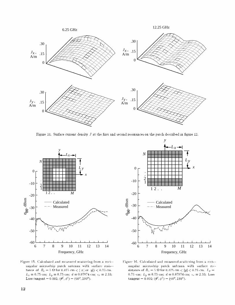
described in gure 12 at the two resonant peaks areshown in gure 14 and are similar to those shown pre-
viously for patches with a constant surface resistance.
A similar patch and the accompanying results are
shown in gure 15. In this case the patch is perfectly
conducting in the center and has a 5 surface re-
sistance around the perimeter. The resonant peaksin the response are lower than those of the previous
response, as is expected with the addition of resis-
L y
Lx
x
y
1 2 . . M
12..
N
6 7 8 9 10 11 12 13 14-50
-40
-30
-20
Frequency, GHzσ
, d
Bsm
θθ
M = N = 12M = N = 16
5 Ω
20 Ω
100 Ω
Figure 13. Calculated results of scattering from a rect-
angular microstrip patch antenna with surface re-sistance Rs for 0:375 cm< (jxj and jyj) < 0:75 cm.
Lx = 0:75 cm; Ly = 0:75 cm; d = 0:07874 cm; r = 2:33;
Loss tangent = 0:001; (i;i) = (60; 180).
tive material on a greater portion of the patch. A
microstrip patch with a 5 surface resistivity on the
patch edges is shown in gure 16. The resistance in
this case is on the patch edges that have the highercurrent density for the given excitation. A similar
patch is shown in gure 17, but in this case the 5
surface resistance is on the patch edges that have the
lower current density for the given excitation. It is in-
teresting to note that the rst resonance in gure 16is considerably lower than the rst resonance in g-
ure 17, although the levels at the second resonance
for each case are nearly the same. A similar patch is
shown in gure 18, but the surface resistance on one
of the patch edges has been increased to 20 . Thepredicted shape of the response can be seen in the
measured data, although a frequency shift is clearly
evident. As expected, with the increase in the sur-
face resistance on the patch the level of the scattered
eld decreases. As a nal example, a patch that has
a 5 surface resistance above the diagonal and isperfectly conducting below the diagonal has been an-
alyzed. This is shown in gure 19 along with the cal-
culated and measured radar cross section . The
data show close agreement on the lower portion of
11
.30
.15
0
6.25 GHz
.30
.15
0
12.25 GHz
.30
.15
0
.30
.15
0
J ,A/m
xJ ,A/m
x
J ,A/m
yJ ,A/m
y
Figure 14. Surface current density J at the rst and second resonances on the patch described in gure 12.
L y
Lx
x
y
1 2 . . M12..
N
6 7 8 9 10 11 12 13 14
Frequency, GHz
σ
, dB
smθθ
CalculatedMeasured
-50
-40
-30
-20
-10
0
-60
Figure 15. Calculated and measured scattering from a rect-
angular microstrip patch antenna with surface resis-
tance of Rs = 5 for 0:375 cm< (jxj or jyj) < 0:75 cm.Lx = 0:75 cm; Ly = 0:75 cm; d = 0:07874 cm; r = 2:33;
Loss tangent = 0:001; (i; i) = (60; 180).
Ly
Lx
x
y
1 2 . . M
12..
N
6 7 8 9 10 11 12 13 14
-50
-40
-30
Frequency, GHz
σ
, dB
smθθ
CalculatedMeasured
-20
-10
0
-60
Figure 16. Calculated and measured scattering from a rect-
angular microstrip patch antenna with surface re-
sistance of Rs = 5 for 0:375 cm< jyj < 0:75 cm. Lx =0:75 cm; Ly = 0:75 cm; d = 0:07874 cm; r = 2:33; Loss
tangent = 0:001; (i;i) = (60;180).
12

Ly
Lx
x
y
1 2 . . M
12..
N
6 7 8 9 10 11 12 13 14
-50
-40
-30
Frequency, GHz
σ
, dB
smθθ
CalculatedMeasured
-20
-10
0
-60
Figure 17. Calculated and measured scattering from a rect-
angular microstrip patch antenna with surface resistance
of Rs = 5 for 0:375 cm < jxj < 0:75 cm. Lx = 0:75 cm;Ly = 0:75 cm; d = 0:07874 cm; r = 2:33; Loss tangent =
0:001; (i; i) = (60; 180).
L y
Lx
x
y
1 2 . . M12..
N
6 7 8 9 10 11 12 13 14
-50
-40
-30
Frequency, GHzσ
, d
Bsm
θθ
CalculatedMeasured
-20
-10
0
-60
Figure 18. Calculated and measured scattering from a rect-
angular microstrip patch antenna with surface resis-
tance of Rs = 5 for 0:75 cm< x < 0:375 cm andRs = 20 for 0:375 cm < x < 0:75 cm. Lx = 0:75 cm;
Ly = 0:75 cm; d = 0:07874 cm; r = 2:33; Loss tangent =
0:001; (i;i) = (60; 180).
L y
Lx
x
y
1 2 . . M
12..
N
6 7 8 9 10 11 12 13 14
-50
-40
-30
Frequency, GHz
σ
, dB
smθθ
CalculatedMeasured
-20
-10
0
-60
Figure 19. Calculated and measured scattering from a rectangular microstrip patch antenna with surface resistance of
Rs = 5 above the patch diagonal. Lx = 0:75 cm; Ly = 0:75 cm; d = 0:07874 cm; r = 2:33; Loss tangent = 0:001;(i; i) = (60; 180).
13

the frequency band but have some dierences on the
upper portion of the frequency band. As before, this
was thought to have been caused by imperfections of
the patch shape.
Conclusions
This paper has described scattering from rectan-
gular microstrip patches with a surface resistance Rs
that is allowed to vary as a function of position on the
patch surface. The boundary condition for the elec-
tric eld was used to derive an integral equation for
the electric current that resides on the patch surface.
Piecewise linear subdomain basis functions were used
to model the current distribution on the patch sur-
face. The necessary terms for representing the sur-
face resistance on the patch were derived and were
included in the equation in the form of a resistance
matrix. The system of equations was then solved
with standard solution techniques available on the
computer.
A variety of test cases were performed to ensure
the validity of the theory and the accuracy of the
computer codes. First, test cases were run for patches
with a constant surface resistance. Additional cases
were then run for patches with a surface resistance
that varied as a function of position on the patch
surface. Scattering results, , measured in the Ex-
perimental Test Range at the Langley Research Cen-
ter were compared with the predicted values. In
all cases satisfactory agreement between the mea-
sured data and the calculated data was noted. How-
ever, slight dierences were seen in some cases and
have been attributed to physical imperfections of the
patch shapes, the nite size of the ground plane used,
and errors in the radar range background subtraction
process. Scattering results for other polarizations
have also been calculated and presented.
The addition of resistance on the surface of a
microstrip patch antenna has been shown to decrease
the scattered energy from the antenna. A resis-
tance of 20 on the entire surface of the patch to-
tally removed the sharp resonant peaks evident in
the frequency response of the perfectly conducting
patch. In addition to reducing the scattering from a
microstrip patch antenna, it may also be possible to
increase the impedance bandwidth of the antenna
with resistance on the antenna surface if the decrease
in the antenna gain can be tolerated.
NASA Langley Research Center
Hampton, VA 23681-0001
May 24, 1993
References
1. Bailey, M. C.; and Deshpande, M. D.: Integral Equation
Formulationof MicrostripAntennas. IEEE Trans. Anten-
nas & Propag., vol. AP-30, no. 4, July 1982, pp. 651656.
2. Deshpande,M. D.; and Bailey,M. C.: Input Impedance of
Microstrip Antennas. IEEE Trans. Antennas& Propag.,
vol. AP-30, no. 4, July 1982, pp. 645650.
3. Bailey, M. C.; and Deshpande, M. D.: Analysis of Rect-
angular Microstrip Antennas. NASA TP-2276, 1984.
4. Pozar, David M.: Input Impedance and Mutual Cou-
pling of Rectangular Microstrip Antennas. IEEE Trans.
Antennas & Propag., vol. AP-30, no. 6, Nov. 1982,
pp. 11911196.
5. Pozar, David M.; and Schaubert, Daniel H.: Analysis of
an Innite Array of RectangularMicrostripPatchesWith
Idealized Probe Feeds. IEEE Trans. Antennas& Propag.,
vol. AP-32, no. 10, Oct. 1984, pp. 11011107.
6. Aberle, J. T.; and Pozar, D. M.: Radiation and Scat-
tering From Circular Microstrip Patches. Antennas and
Propagation|1989 IEEE APS InternationalSymposium,
Volume I, IEEE Catalog No. CH2654-2/89, IEEE Anten-
nas and Propagation Soc., 1989, pp. 438441.
7. Aberle, James T.; and Pozar, David M.: Analysis of
Innite Arrays of One- and Two-Probe-Fed Circular
Patches. IEEE Trans. Antennas& Propag., vol. 38, no. 4,
Apr. 1990, pp. 421432.
8. Aberle, J. T.; and Pozar, D. M.: Analysis of Innite Ar-
rays of Probe-Fed Rectangular Microstrip Patches Using
a Rigorous Feed Model. IEE Proc., pt. H, vol. 136, no. 2,
Apr. 1989, pp. 110119.
9. Aberle, James T.; and Pozar, David M.: Accurate and
Versatile Solutions for Probe-Fed Microstrip Patch An-
tennas and Arrays. Electromagnetics, vol. 11, no. 1,
Jan.Mar. 1991, pp. 119.
10. Pozar, David M.: Radiationand ScatteringFrom a Micro-
strip Patch on a Uniaxial Substrate. IEEE Trans. Anten-
nas & Propag., vol. AP-35, no. 6, June 1987, pp. 613621.
11. Aberle, James T.; Pozar, David M.; and Birtcher,
CraigR.: Evaluationof Input Impedanceand RadarCross
Section of Probe-FedMicrostripPatch Elements Using an
Accurate Feed Model. IEEE Trans. Antennas& Propag.,
vol. 39, no. 12, Dec. 1991, pp. 16911696.
12. Newman,Edward H.; and Forrai, David: ScatteringFrom
a Microstrip Patch. IEEE Trans. Antennas & Propag.,
vol. AP-35, no. 3, Mar. 1987, pp. 245251.
13. Jackson, David R.: The RCS of a Rectangular Microstrip
Patch in a Substrate-SuperstrateGeometry. IEEE Trans.
Antennas& Propag., vol. 38, no. 1, Jan. 1990, pp. 28.
14. Bailey, M. C.; and Deshpande, M. D.: Analysis of El-
liptical and Circular Microstrip Antennas Using Moment
Method. IEEE Trans. Antennas& Propag., vol. 33, no. 9,
Sept. 1985, pp. 954959.
15. Hansen, V.; and Janhsen, A.: Spectral Domain Anal-
ysis of Microstrip Arrays Including the Feed Network
14

With Space-Varying Surface Impedances and Lumped El-
ements. Electromagnetics, vol. 11, no. 1, Jan.Mar. 1991,
pp. 6988.
16. Hall, Richard C.; and Mosig, Juan R.: The Analy-
sis of Coaxially Fed Microstrip Antennas With Electri-
cally Thick Substrates. Electromagnetics, vol. 9, 1989,
pp. 367384.
17. Hall, R. C.; and Mosig, J. R.: The Calculation of Mu-
tual Coupling Between Microstrip Antennas With Thick
Substrates. 1989 International Symposium Digest|
Antennas and Propagation, Volume I, IEEE Catalog No.
CH2654-2/89, IEEE Antennas and Propagation Soc.,
1989, pp. 442445.
18. Mosig, Juan R.: ArbitrarilyShapedMicrostrip Structures
and Their AnalysisWith aMixed Potential IntegralEqua-
tion. IEEE Trans. Microw. Theory& Tech., vol. 36, no. 2,
Feb. 1988, pp. 314323.
19. Mosig, J. R.; and Gardiol, F. E.: General Integral Equa-
tion Formulation for Microstrip Antennas and Scatterers.
IEE Proc., pt. H, vol. 132, no. 7, Dec. 1985, pp. 424432.
20. Senior, T. B. A.: Scattering by Resistive Strips. Radio
Sci., vol. 14, no. 5, Sept.Oct. 1979, pp. 911924.
21. Senior, T. B. A.: Backscattering From Resistive Strips.
IEEE Trans. Antennas & Propag., vol. AP-27, no. 6,
Nov. 1979, pp. 808813.
22. Senior, Thomas B. A.: Approximate Boundary Condi-
tions. IEEE Trans. Antennas & Propag., vol. AP-29,
no. 5, Sept. 1981, pp. 826829.
23. Senior, Thomas B. A.: Combined Resistive and Conduc-
tive Sheets. IEEE Trans. Antennas& Propag., vol. AP-
33, no. 5, May 1985, pp. 577579.
24. Senior, T. B. A.; and Liepa, V. V.: Backscattering
From Tapered Resistive Strips. IEEE Trans. Antennas
& Propag., vol. AP-32, no. 7, July 1984, pp. 747751.
25. Hall, R. C.; and Mittra, R.: Scattering From a Periodic
Array of Resistive Strips. IEEE Trans. Antennas &
Propag., vol. AP-33, no. 9, Sept. 1985, pp. 10091011.
26. Haupt, Randy L.; and Liepa, Valdis V.: Synthesis of Ta-
pered Resistive Strips. IEEE Trans. Antennas& Propag.,
vol. AP-35, no. 11, Nov. 1987, pp. 12171225.
27. Haupt, Randy L.; and Liepa, Valdis V.: Resistive Ta-
pers That Place Nulls in the Scattering Patterns of
Strips. IEEE Trans. Antennas& Propag., vol. 38, no. 7,
July 1990, pp. 11171119.
28. Rubin, B. J.; and Bertoni, H. L.: Re ection From a
Periodically Perforated Plane Using a Subsectional Cur-
rent Approximation. IEEE Trans. Antennas & Propag.,
vol. AP-31, no. 6, Nov. 1983, pp. 829836.
29. Cwik, Thomas A.; and Mittra, Raj: Scattering From
a Periodic Array of Free-Standing Arbitrarily Shaped
Perfectly Conducting or Resistive Patches. IEEE Trans.
Antennas & Propag., vol. AP-35, no. 11, Nov. 1987,
pp. 12261234.
30. Chang, Albert; and Mittra, Raj: Using Half-Plane So-
lutions in the Context of MM for Analyzing Large Flat
Structures With or Without Resistive Loading. IEEE
Trans. Antennas& Propag., vol. AP-38, no. 7, July 1990,
pp. 10011009.
31. Shalaby, Abdel-Aziz T. K.: Spectral Domain Formula-
tion for SuperconductingMicrostripLinesWithArbitrary
Strip Thickness. IEEE Antennas and Propagation Soci-
ety InternationalSymposium|1992 Digest, VolumeTwo,
IEEE Catalog No. 92CH3178-1, IEEE Antennas and
Propagation Soc., 1992, pp. 990993.
32. Lyons, W. G.; and Oates, D. E.: MicrowaveCharacteriza-
tion of High-Tc SuperconductingThin Films and Devices.
IEEE Antennas and Propagation Society International
Symposium|1992 Digest, Volume Four, IEEE Catalog
No. 92CH3178-1, IEEE Antennas and Propagation Soc.,
1992, p. 2256.
15

REPORT DOCUMENTATION PAGEForm Approved
OMB No. 0704-0188
Public reporting burden for this collection of information is estimated to average 1 hour per response, including the time for reviewing instructions, searching existing data sources,gathering and maintaining the data needed, and completing and reviewing the collection of information. Send comments regarding this burden estimate or any other aspect of thiscollection of information, including suggestions for reducing this burden, toWashington Headquarters Services, Directorate for Information Operations and Reports, 1215 JeersonDavis Highway, Suite 1204, Arlington, VA 22202-4302, and to the Oce of Management and Budget, Paperwork Reduction Project (0704-0188), Washington, DC 20503.
1. AGENCY USE ONLY(Leave blank) 2. REPORT DATE 3. REPORT TYPE AND DATES COVERED
August 1993 Technical Paper
4. TITLE AND SUBTITLE
Analysis of Microstrip Patch Antennas With Nonzero Surface
Resistance
6. AUTHOR(S)
David G. Shively and M. C. Bailey
7. PERFORMING ORGANIZATION NAME(S) AND ADDRESS(ES)
Joint Research Program Oce NASA Langley Research Center
Electronics Integration Directorate Hampton, VA 23681-0001
Communications Electronics Command
Langley Research Center
Hampton, VA 23681-0001
9. SPONSORING/MONITORING AGENCY NAME(S) AND ADDRESS(ES)
U.S. Army Communications Electronics Command
Fort Monmouth, NJ 07703-5603and
National Aeronautics and Space Administration
Washington, DC 20546-0001
5. FUNDING NUMBERS
WU 505-64-20-54
P1L162211AH85
8. PERFORMING ORGANIZATION
REPORT NUMBER
L-17219
10. SPONSORING/MONITORING
AGENCY REPORT NUMBER
NASA TP-3362
CECOM TR-93-E-2
11. SUPPLEMENTARY NOTES
Shively: Joint Research Program Oce, EID-CECOM, Langley Research Center, Hampton, VA;Bailey: Langley Research Center, Hampton, VA.
12a. DISTRIBUTION/AVAILABILITY STATEMENT 12b. DISTRIBUTION CODE
UnclassiedUnlimited
Subject Category 32
13. ABSTRACT (Maximum 200 words)
The scattering properties of a microstrip patch antenna with nonzero surface impedance are examined. Theelectric eld integral equation for a current element on a grounded dielectric slab is developed for a rectangulargeometry by using Galerkin's technique with subdomain piecewise linear basis functions. The integral equationincludes a resistive boundary condition on the surface of the patch. The incident eld on the patch is expressedas a function of incidence angle. The resulting system of equations is then solved for the unknown currentmodes on the patch, and the radar cross section is calculated for a given scattering angle. Theoretical resultsin the form of radar cross section as a function of frequency are compared with results measured at the NASALangley Research Center.
14. SUBJECT TERMS 15. NUMBER OF PAGES
Antennas; Scattering; Surface resistance 16
16. PRICE CODE
A0317. SECURITY CLASSIFICATION 18. SECURITY CLASSIFICATION 19. SECURITY CLASSIFICATION 20. LIMITATION
OF REPORT OF THIS PAGE OF ABSTRACT OF ABSTRACT
Unclassied Unclassied
NSN 7540-01-280-5500 Standard Form 298(Rev. 2-89)Prescribed by ANSI Std. Z39-18298-102