nap (no alu processor) : the great communicator
TRANSCRIPT
JOURNAL OF PARALLEL AND DISTRIBUTED COMPUTING 8,169- 179 ( 1990)
NAP (No ALU Processor): The Great CommunicatorBRADLEY C. KUSZMAUL*
Massachusetts Institute of Technology. Laboratoryfor Computer Science, Cambridge, Massachusetts 02139
A N D
JEFF FRIED+
Massachusetts Institute ofTechnology, Laboratoryfor Computer Science, Cambridge, Massachusetts 02139:and GTE Laboratories, Waltham, Massachusetts 02254
Message routing networks are acknowledged to be one of themost critical portions of massively parallel computers. This pa-per presents a processor chip for use in a massively parallel com-puter. The programmable approach used in this processor pro-vides enough f lexibi l i ty to make i t a “universal” part for bui ldinga wide variety of interconnection networks and routing algo-rithms. A SIMD control scheme is used to make programmingand synchronizing large numbers of processors simple. In thecourse of designing this processor, we were faced with the deci-sion of which logic operations to implement in an Arithmetic-Logic Unit (ALU); informal design studies showed that it wasbest to provide none. The processor performs al l computationsby a sophist icated table lookup mechanism, and has no ALU; i tis thus called the No ALU Processor (NAP). Using tables ratherthan an ALU provides a very flexible instruction set , and in realprograms often allows more than one “operation” to be done inone cycle. Benchmarks written for the NAP show that indirectaddressing mechanisms can speed many common operations bya factor of about log N on an N-processor machine. We havetherefore provided hardware to support indirect addressing, ora Multiple Address Multiple Data operation. In addition, theNAP contains local storage used for flexible instructiondecoding: the same instruction can result in different operat ionson different chips. These two mechanisms allow programmersto write programs for NAP machines easily using SIMD style,and also provide the power of different computations happeningsimultaneously in different parts of the machine. It is possibleto build and eff iciently simulate, using NAP chips, a wide varietyof communications networks, including hypercubes, butterf l ies ,fat-trees, and networks for computing parallel prefix operations.By this informal measure, the NAP architecture is a universalpart for building interconnection networks and running networkalgorithms. 0 1990 Academic Press, Inc.
* Partially supported by ONR, Reference Number NO00 14-83-K-O 125,and by ONR, Reference Number NO00 14-84-K-0099.
t Supported by GTE Laboratories, DARPA Contract NOOO14-87-K-0825, and ONR Contract NOOO14-86-K-0593.
I. INTRODUCTION
Message routing networks for parallel supercomputersoccupy a unique place in the spectrum from specialized togeneral-purpose machines. Although these routing net-works can be used to build general-purpose parallel com-puters (as well as specialized computers), they themselvesare usually built out of very specialized hardware. This pa-per presents a single processor design which is useful forbuilding a variety of different networks; in this sense it is ageneral-purpose element within the specialty of intercon-nection networks. This processor is an experimental designincorporating several novel architectural features whichmake it simple to program, general purpose, and efficient.Specifically, no Arithmetic-Logic Unit (ALU) is providedin the processor. The arithmetic functions normally per-formed by an ALU are instead performed by table lookupsinto memory. In addition, a very flexible programmingmodel is provided, which supports indirect addressing andmultiple concurrent instructions while operating in a Sin-gle-Instruction Multiple-Data (SIMD) mode or MultipleSIMD (MSIMD) mode.
The No ALU Processor (NAP) chip described in this pa-per is the result of a design experiment which explores archi-tectures for communication network support. The experi-ment has three main design goals:
l Act as a “universal” element for routing networks. Byuniversal we mean both general purpose and efficient. Theperformance of the NAP when used as a node within a net-work should be as close as possible to the performance of aspecial-purpose chip designed especially for that network.
l Provide communications control which is as flexible aspossible.
l Keep the processor’s input-output channels (whichconnect to other NAP chips) and memory as busy as possi-ble performing useful work.
1 6 9 0743-7315/90$3.00Copyright 0 1990 by Academic Press, Inc.
All rights of reproduction in any form reserved.
170 KUSZMAUL AND FRIED
In the course of designing the NAP, we were faced withthe decision of which logic operations to implement in anALU; informal design studies showed that it was best to pro-vide none. Using tables rather than an ALU provides a veryflexible instruction set, and in real programs often allowsmore than one “operation” to be done in one cycle. One ofthe most interesting lessons from the design of the NAP wasthat table lookup is a very powerful mechanism.
It is interesting to note that there are two other examplesof ALU-less processors, both from the early 1960s. One ofthese, called the CADET, was built and marketed by IBM[ 11. The other was proposed by Ferroxcube Corp. [ 91, amanufacturer of core memory. Both of these machines wereexplored because the cost and performance of memory hadbeen greatly improved with the invention of core memory.As the density of memory compared to logic continues toincrease, a somewhat similar situation exists today.
A collection of NAP chips can be wired together and canbe programmed to simulate many things. We have pro-grammed our simulators to perform several important par-allel algorithms, including reduction and parallel prefix ina tree network [ 21, connection-machine style routing on acube-connected cycle [ 5 1, and cellular automata programs(such as Conway’s game of Life) [ 111. We are able to sup-port any network with a large number of nodes (up to about2 32 nodes) of constant degree, including fat-trees [ 6, 41,butterfly networks [ 12,8, lo], cube-connected cycles, trees,and meshes.
Section II of this paper describes the instruction set archi-tecture of the NAP. Section III gives three examples of theprogramming and operation of the NAP. Section IV dis-cusses the implementation of the NAP chip. Finally, Sec-tion V evaluates the NAP in the light of our design goals,and summarizes the lessons learned from this project.
II. INSTRUCTION SET ARCHITECTURE
We adopt the (M)SIMD model, where one or more mi-crocontrollers broadcast microinstructions to sets of proces-sors; each set of processors is controlled by one microcon-troller. The microcontroller handles all instruction se-quencing (e.g., loops and branches) and, as such, must beas powerful as a conventional computer. In this SIMDmodel all processors are globally synchronized at the in-struction level.
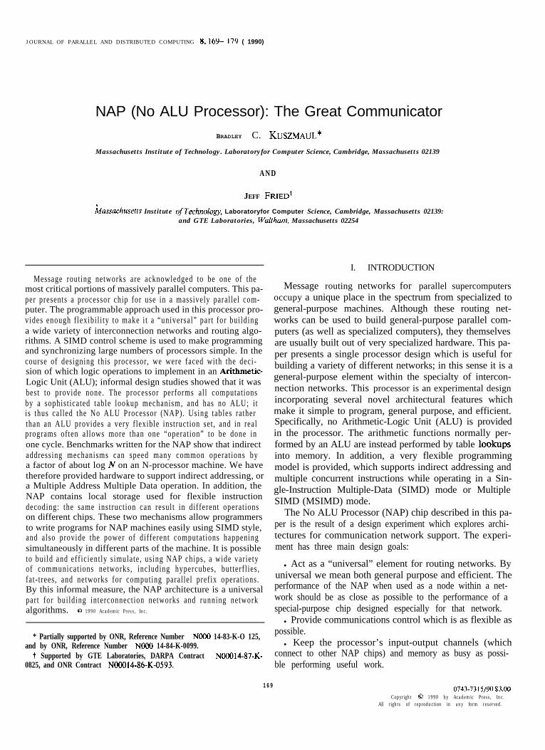
A top-level view of a NAP computer system is shown inFig. 1. Global microcontrollers broadcast instructions (asingle microcontroller is shown at the left) to collections ofNAP chips (shown at the right). Each NAP is connected toits neighbors through up to eight bidirectional data chan-nels. Each bidirectional data channel is capable of sending1 bit and receiving 1 bit per clock cycle. The NAP proces-sors also have an off-chip static random access memory(SRAM).
FIG. 1. System-level view of a NAP-based computer. Global micro-controllers broadcast instructions to sets of NAP chips. Each NAP chip isconnected to an off-chip SRAM, a SIMD instruction broadcast bus, andeight bidirectional network lines.
The bidirectional channels may be connected in any fash-ion to form an interconnection network; the NAP chipsform the nodes of that network, and may do computationsin parallel to perform routing, do actual computing for thesystem, or both. Examples of networks which can be builtusing NAPS are butterfly or fat-tree networks, banyan orflip-type networks, hypercubes (more than 2 8 processors re-quire multiple NAPS per node), cube-connected cycles,shuffle-exchange networks; torus and mesh networks, re-structurable networks, and trees. One restriction is that thenetworks are regular enough to have fewer than 16 distincttypes of nodes; most practical networks have 1 or 2.
A. Indirect Addressing and MIMD
One very important mechanism provided by the NAPwhich is not found in conventional SIMD computers is in-direct addressing. We support indirect addressing becauseof the wave nature of the computations performed by manyrouting networks. Consider, for example, parallel prefix[ 2 1, which is a class of parallel algorithms which use a treeinterconnection structure between processors to performmany operations (such as addition) in log N time on Npro-cessors. At any stage of a parallel prefix computation,different levels of the tree may be accessing bits at differentaddresses. Conventionally, this would be handled by en-abling or disabling the processors at different levels of thetree, and running the computation on different levels atdifferent times, thus slowing down the overall computationto time log* N. Indirect addressing provides a mechanismfor different processors to access different memory ad-dresses at the same time under SIMD control. The result is
NAP: THE GREAT COMMUNICATOR 171
that parallel programming can be done more flexibly andmore efficiently (by a factor of log N).
In addition to indirect addressing, there are three meansof differentiating processors within the SIMD control struc-ture and hence making programming more flexible andefficient:
1. Conditional execution: the instructions broadcast onthe SIMD bus can conditionally load a local instructionstore called the nanostore, conditionally load the memory,conditionally load configuration bits within the NAP(called Input-or-State-Select or ISS bits), and conditionallyexecute sequences of instructions. An instruction may beconditionally executed depending on a combination ofstate bits and data from the input channel.
2. The instructions stored within the nanostore of eachNAP may be different, so that different processors may per-form totally different operations in response to the samebroadcast instruction.
3. Processors can have different tables at the same ad-dress in local memory, and thus perform different functionseven while they are accessing the same address.
These three mechanisms, which are explained in more de-tail below, provide a large degree of flexibility to NAP pro-grammers.
B. Instruction Philosophy
We assume that off-chip wire delays are large comparedto on-chip cycle times and local memory access time, sincewe are implementing systems with long wires (we use a ca-pacitive model for the wires). Therefore, we chose an ap-proach where there is a slow clock for operations betweenprocessors (the microcycle) and a fast clock for operationswithin a processor (the nanocycle). During one microcycle,the microcontroller broadcasts a microinstruction, which isexecuted by the processors. Each processor can read or writefrom each of its eight single-bit input-output channels. Dur-ing one microcycle, there are four minor cycles called nano-cycles. During one nanocycle, a nanoinstruction is exe-cuted. A nanoinstruction may access the external memorywith a read-modify-write (which gives the processor the oldvalue in memory and allows the processor to modify 1 bitof memory or to write a complete different value back tomemory). The nanoinstruction also updates some internalprocessor state. The memory address may be changed onceper nanocycle.
The NAP depends heavily on memory. As we have seen,a nanocycle may involve a complex memory access, so thatthe performance of the NAP is driven by memory perfor-mance. Most programs written for the NAP are also verymemory-oriented. Operations are performed using tables inmemory under the control of broadcast microinstructions.Typically, these table-based operations take as operands an
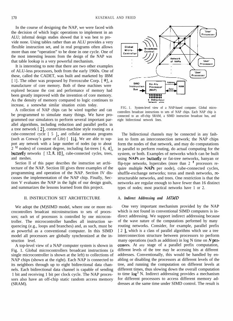
arbitrary combination of state and input channel values, aninteger, or an address. Each table (called a function table)requires 256 words ( 8 bits each). An example function ta-ble for adding two 2-bit numbers is shown in Fig. 2. Notethat multiple functions can be combined in one table; thetable shown in Fig. 2 has a number of unused bits (denotedby “X”) that could be used for another function. Our proto-type supports up to 2K words of external SRAM, so that upto eight different tables can be stored in memory at once;additional tables are downloaded as needed. Tables may beaccessed using either direct or indirect addressing.
We adopted the principle that the implementationshould allow as much flexibility as possible, unless thatflexibility would be expensive. For example, we tried toavoid making any of the state bits special, but we needed 2state bits to control the conditionalization. We decided thatadding a multiplexor or increasing the width of the CC fieldto allow full generality would be too expensive. The condi-tionalization of processors is very general, since it is doneby table lookup in the 4-bit CC field.
C. The NAP Microword
Table I shows the format of the NAP microword. Thisword is the instruction broadcast from a microcontroller toa number of NAP chips in ( M )SIMD fashion each micro-cycle. The 39 bits of the microword are common to all theNAPS in a set. Each microword contains distinct operationcodes for every nanocycle, as well as condition codes, a di-rect memory address, and two table offsets used for indirectaddressing or table-based logical operations. The mi-
Word Addressxxxx 00 00xxxx 00 01xxxx 00 10xxxx 00 11xxxx 01 00xxxx 01 01xxxx 01 10xxxx 01 11xxxx 10 00xxxx 10 01xxxx 10 10xxxx 10 11xxxx 11 00xxxx 11 01xxxx 11 10xxxx 11 11
outputxxxxx 000xxxxx 001xxxxx 010xxxxx 011xxxxx 001xxxxx 010xxxxx 011xxxxx 100xxxxx 010xxxxx 011xxxxx 100xxxxx 101xxxxx 011xxxxx 100xxxxx 101xxxxx 110
FIG. 2. Example function table for two-input 2-bit addition. The wordaddress is composed of some unused high-order bits (which could be usedfor another function), and two binary 2-bit inputs. The output consists of5 unused high-order bits, and a 3-bit result. Unused bits are denoted by“x”. Note that each line of this description specifies 16 words of the func-tion table.
172 KUSZMAUL AND FRIED
TABLE I ent processors. The OP fields give the “address” of theThe Microinstruction Word Format Shows the Mnemonics, nanoinstruction within the nanostore. This approach re-
Functions, and Width of Each Instruction Field duces the number of bits broadcast to the processors andthus economizes on chip pins. In addition, it provides a
WidthMnemonic Function (bits)
mechanism for different processors to perform differentwork under the control of the same microinstruction, since
INIT Initialization and download control 2different processors may have different nanoinstructions
OPO Four-bit indexes into the nanostore which loaded into the same address in the nanostore.OPI specify which nanoinstruction to perform
4
OP2 in each nanocycle; OPs share one address44 D. Processor Organization
OP3 and condition code 4c c Condition code; this decodes to 16 conditions 4
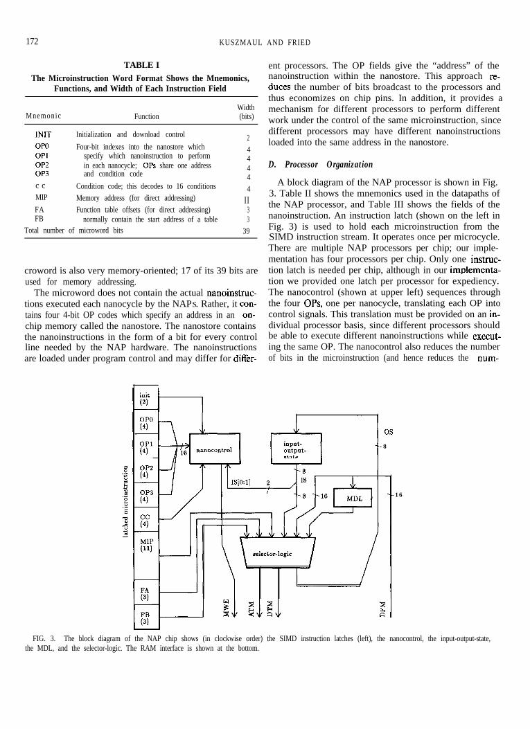
A block diagram of the NAP processor is shown in Fig.MIP Memory address (for direct addressing) II
3. Table II shows the mnemonics used in the datapaths of
FA Function table offsets (for direct addressing) 3 the NAP processor, and Table III shows the fields of theFB normally contain the start address of a table 3 nanoinstruction. An instruction latch (shown on the left in
Total number of microword bits 39 Fig. 3) is used to hold each microinstruction from theSIMD instruction stream. It operates once per microcycle.There are multiple NAP processors per chip; our imple-mentation has four processors per chip. Only one instruc-
croword is also very memory-oriented; 17 of its 39 bits are tion latch is needed per chip, although in our implementa-used for memory addressing. tion we provided one latch per processor for expediency.
The microword does not contain the actual nanoinstruc- The nanocontrol (shown at upper left) sequences throughtions executed each nanocycle by the NAPS. Rather, it con- the four OPs, one per nanocycle, translating each OP intotains four 4-bit OP codes which specify an address in an on- control signals. This translation must be provided on an in-chip memory called the nanostore. The nanostore contains dividual processor basis, since different processors shouldthe nanoinstructions in the form of a bit for every control be able to execute different nanoinstructions while execut-line needed by the NAP hardware. The nanoinstructions ing the same OP. The nanocontrol also reduces the numberare loaded under program control and may differ for differ- of bits in the microinstruction (and hence reduces the num-
OS
- 8
- 1 6
FIG. 3. The block diagram of the NAP chip shows (in clockwise order) the SIMD instruction latches (left), the nanocontrol, the input-output-state,the MDL, and the selector-logic. The RAM interface is shown at the bottom.
NAP: THE GREAT COMMUNICATOR 173
TABLE II logic produces the address to memory (ATM), data toMnemonics Used in the Datapaths of the NAP Processor memory (DTM), and data to the input-output-state (OS).
Mnemonic Description
ATM Address To MemoryDFM Data From MemoryDTM Data To MemoryBITADDR BIT ADDRessBITVAL BIT VALueI data from Input channels0 data to Output channelsS State dataIS combined Input-State dataOS combined Output-State dataM M Mix-and-Match valueISS Input-State-Select (register)MDL Memory-Data-Latch (register)
Width(bits)
II883188888888
ber of pins per chip) since each of the four nanoinstructionsis encoded into 4 rather than 28 bits.
Within each nanocycle the NAP processor behaves as fol-lows (refer to Fig. 3 ) . The data flow through the NAP cir-cuitry as follows. Each nanocycle, the selector-logic uses theMIP, FA, and FB fields of the microinstruction, the currentvalue of the MDL, and the current IS value (derived fromthe S-bit state register and the data input pads) to computea memory address (ATM, shown leaving downward fromthe selector logic). The memory responds with data frommemory (DFM, shown arriving at the lower right). Thevalue of DFM is supplied to the MDL and the selector-logic.The selector-logic then uses the previously available dataplus the value of DFM to compute new DTM. The value ofDTM may be written to the same memory location indexedby the memory address generated earlier in the nanocycle.Whether DTM is actually written to memory is controlledby the memory-write-enable ( MWE, which is a 1 -bit nano-instruction field). The DTM and MWE signals are shownleaving at bottom center.
The input-output-state (shown at upper right) controlsall the input-output data channels (i.e., wires) for the pro-cessor. Each input-output-state unit can be individuallyprogrammed to act as a bidirectional input-output channelor as a single bit of internal state.
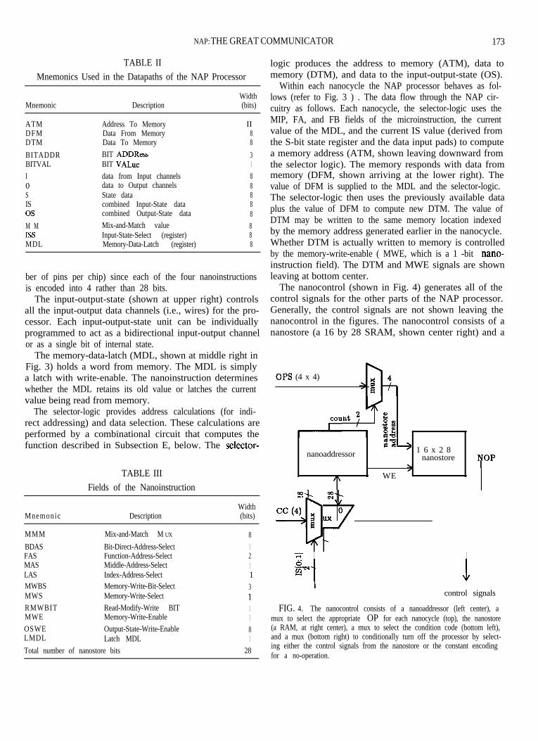
The nanocontrol (shown in Fig. 4) generates all of thecontrol signals for the other parts of the NAP processor.Generally, the control signals are not shown leaving thenanocontrol in the figures. The nanocontrol consists of ananostore (a 16 by 28 SRAM, shown center right) and a
The memory-data-latch (MDL, shown at middle right inFig. 3) holds a word from memory. The MDL is simplya latch with write-enable. The nanoinstruction determineswhether the MDL retains its old value or latches the currentvalue being read from memory.
OPS (4 x 4)
The selector-logic provides address calculations (for indi-rect addressing) and data selection. These calculations areperformed by a combinational circuit that computes thefunction described in Subsection E, below. The selector-
TABLE IIIFields of the Nanoinstruction
nanoaddressor ‘I* 1 6 x 2 8nanostore
>
TWE
Mnemonic Description
MMM Mix-and-Match M UX
BDAS Bit-Direct-Address-SelectFAS Function-Address-SelectMAS Middle-Address-SelectLAS Index-Address-SelectMWBS Memory-Write-Bit-SelectMWS Memory-Write-SelectRMWBIT Read-Modify-Write BITMWE Memory-Write-EnableOSWE Output-State-Write-EnableLMDL Latch MDLTotal number of nanostore bits
Width(bits)
81211311181
28
-yccc4q) ILi- I I
control signals
FIG. 4. The nanocontrol consists of a nanoaddressor (left center), amux to select the appropriate OP for each nanocycle (top), the nanostore(a RAM, at right center), a mux to select the condition code (bottom left),and a mux (bottom right) to conditionally turn off the processor by select-ing either the control signals from the nanostore or the constant encodingfor a no-operation.
174 KUSZMAUL AND FRIED
nanoaddressor (shown center left ) , which is essentially a 2-bit counter with some extra control logic. The value of the2-bit counter is used to select which of the four OPs to use.The selected OP (a 4-bit value) is used to address 1 of the16 words of the nanostore (shown center right). One of thefour CC bits from the microinstruction is selected by thelow-order 2 bits of IS to conditionalize the processor. If theprocessor is disabled (the CC bit is zero), then the controlsignals are set to values which result in no state change, andif the processor is active (the CC bit is one), the outputs ofthe nanostore are the control bits used directly by the logicin the processor.
SIMD instruction stream (rather than, e.g., through a diag-nostic scan path) so that the initialization can be done inparallel. The details of the initialization circuitry are not de-scribed in this paper.
E . The Function Computed by the Selector-Logic
A number of memory addressing modes and data selec-
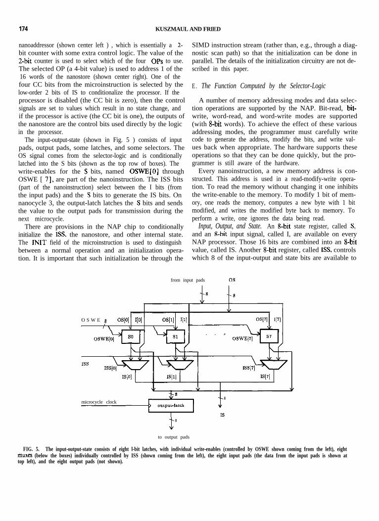
The input-output-state (shown in Fig. 5 ) consists of inputpads, output pads, some latches, and some selectors. TheOS signal comes from the selector-logic and is conditionallylatched into the S bits (shown as the top row of boxes). Thewrite-enables for the S bits, named OSWE[O] throughOSWE [ 71, are part of the nanoinstruction. The ISS bits(part of the nanoinstruction) select between the I bits (fromthe input pads) and the S bits to generate the IS bits. Onnanocycle 3, the output-latch latches the S bits and sendsthe value to the output pads for transmission during thenext microcycle.
tion operations are supported by the NAP. Bit-read, bit-write, word-read, and word-write modes are supported(with g-bit words). To achieve the effect of these variousaddressing modes, the programmer must carefully writecode to generate the address, modify the bits, and write val-ues back when appropriate. The hardware supports theseoperations so that they can be done quickly, but the pro-grammer is still aware of the hardware.
Every nanoinstruction, a new memory address is con-structed. This address is used in a read-modify-write opera-tion. To read the memory without changing it one inhibitsthe write-enable to the memory. To modify 1 bit of mem-ory, one reads the memory, computes a new byte with 1 bitmodified, and writes the modified byte back to memory. Toperform a write, one ignores the data being read.
There are provisions in the NAP chip to conditionally Input, Output, and State. An g-bit state register, called S,initialize the ISS, the nanostore, and other internal state. and an g-bit input signal, called I, are available on everyThe INIT field of the microinstruction is used to distinguish NAP processor. Those 16 bits are combined into an g-bitbetween a normal operation and an initialization opera- value, called IS. Another g-bit register, called ISS, controlstion. It is important that such initialization be through the which 8 of the input-output and state bits are available to
from input pads
O S W E 8 OSIOl I[01 Wll VII
I \ V. . .
microcycle clock8
8
to output pads
FIG. 5. The input-output-state consists of eight l-bit latches, with individual write-enables (controlled by OSWE shown coming from the left), eightmuxes (below the boxes) individually controlled by ISS (shown coming from the left), the eight input pads (the data from the input pads is shown attop left), and the eight output pads (not shown).
NAP: THE GREAT COMMUNICATOR 175
the user as the IS value, according to the following function:ForeachiE{0,...,7},
IS[i] :=I[i] ifISS[i] = 0,
S [ i] otherwise.
The ISS is set under program control.The MDL and the Mix-and-Match Value. An 8-bit regis-
ter called the MDL can be loaded with the DFM on everynanocycle. Whether the MDL latches a new value or keepsits old value is determined by LMDL, a l-bit field in thenanoinstruction.
An 8-bit intermediate value, called MM (for mix-and-match), is a combination of MDL and IS. A programmercan use MM to combine some bits from memory, some bitsfrom input data channels, and some bits from internal state,in order to compute the next state through a table lookup.The value of MM is determined by the following equation:ForeachiE{O,...,7},
MM[i] =IS[i] ifMMM[i] = 0,
MDL [ i] otherwise,
where MMM is an 8-bit field in the nanoinstruction.Generating the Memory Address. The memory address is
used to provide computation via a function table, or to loadand store data from memory. It is an 11 -bit value, generatedas follows:
ATM[O : 41 :=MM[O:4] ifIAS= 1,
MIP [ 0 : 41 otherwise.
ATM[ 5 : 7]:=MM[5 : 71 ifMAS = 1,
MIP[ 5 : 71 otherwise.
if FAS = 0,
ATM[8: lo] := ifFAS = 1,
if FAS = 2.
The definition of MM is given above. The microinstructionprovides MIP, FA, and FB. The nanoinstruction providesIAS, MAS, and FAS. A new memory address is generatedevery nanocycle, although the values of MIP, FA, and FBare held constant for the whole microcycle.
An additional 3 -bit intermediate value called theBITADDR is computed according to the function
BITADDR = I MDL[O : 21 ifBDAS = 1,
FA otherwise,
where BDAS is a l-bit nanoinstruction field. The value of
BITADDR is used to index a single bit inside a byte to im-plement bit-read and bit-write operations.
Generating the Data to Memory (DTM). Every nano-cycle, a byte of data is written back to memory. That byteis computed by the function
1
DFM [ BITADDR + BITVAL]if RMWBIT = 1,
DTM = MM if RMWBIT = 0 and MWS = 0,
OP2 11 OP3 otherwise.
In words, if RMWBIT = 1, we modify the BITADDRth bitof DFM to be BITVAL and store the modified value backto memory. Otherwise we may store the mix-and-matchvalue to memory, or we may store an immediate value (e.g.,for a function table initialization).
A l-bit intermediate value, BITVAL, is computed by
BITVAL = IS [ MWBS] .
The nanoinstruction provides RMWBIT ( 1 bit), MWS ( 1bit), and MWBS ( 3 bits). Except during initialization,MWS is always zero. In one of the initialization modes(indicated by the INIT microinstruction field), only OPO isallowed to execute. In that case, OP2 and OP3 can be usedas immediate data to memory.
Generating OS. The value of OS, which is supplied to theinput-output-state, is computed as
OS =
i
fanout ( DFM [ BITADDR ] )if MWE = 1 and RMWBIT = 1,
DFM otherwise,
where the fanout function produces an 8-bit value from a1 -bit value according to
fanout(0) = 0
fanout( 1) = 255
and where MWE and RMWBIT are both 1 -bit nanoinstruc-tion fields.
F. Providing a Global “OR ” Tree
A global “or” line to the microcontroller (the computerwhich broadcasts the SIMD instruction stream) can be de-rived from any of the output channel bits by ORing onedata output wire from each chip together to compute aglobal “or”. This capability is extremely useful for checkinga global condition (e.g., whether any processor containszero, or whether any processor’s memory contains a patternwhich matches the broadcast pattern). One such global
176 KUSZMAUL AND FRIED
“or” can be returned to the global microcontroller everymicrocycle, although the time between when the microcon-troller broadcasts the microinstruction to when the corre-sponding global “or” arrives back at the microcontrollermay be several microcycles due to pipelining. The distancefrom the microcontroller to the NAP chips through theSIMD bus and back through the global “or” tree might befarther than can be achieved during one microcycle (200ns), so that programmers using the global “or” mechanismmust take account of the pipelining effect. Any data outputpin on the NAP may be used to construct a global “or” tree.In fact, it is possible to have several global “or” trees, bydevoting several data output pins on each NAP to the global“or” tree.
III. PROGRAMMING EXAMPLES
One of the best ways to appreciate the programmingmechanisms provided by the NAP is to study some exampleprograms. Three examples are presented in this section. Foreach example, some tables have been preloaded into the ex-ternal SRAM and some nanoinstructions have been pre-loaded into the nanostore. Each program is one microcyclein length, and the four OPs are bracketed by (OP). Thenotation M[a]jbj] ]c in the following programs indicatesthat a memory reference is being made using an addressbuilt by concatenating bits a, b, and c, where c is the low-order bit.
In our notation, “Mwrite” is the symbol for a memorywrite cycle, and “RMW” indicates a read-modify-write cy-cle (to modify a bit). The latter consists of a read from agiven address in the first phase of a nanocycle, followed bya write of different bits to the same memory address in thesecond phase of the same nanocycle. Finally, the values ofthe condition codes, the MIP field, and the FA and FBpointers are specified.
A. Example 1: Queuing Data in MemoryData queuing is a good example of a need for indirect
addressing; for example, each processor may wish to receiveor send a message at a locally specified address. This pro-gram takes one data input and buffers it in a queue in mem-ory. The input is the bit at IO, and the queue’s tail pointeris at location Q.
OPS=(M[MIP], LatchMDL),
(M[MIP[5:10] llMDL[3:7]],
RMW(IO,MDL[O:2])),
(M[FAIIMDL], LatchMDL),
(MwriteMDLintoM[MIP])
CC=true,MIP=Q,FA=(theINCtable),FB=don't-care
The way this program works is that word Q contains an8-bit “bit pointer” to a bit on the same 256-bit page as Q.During OPO, the MDL is loaded with that bit pointer. Dur-ing OPl, the NAP uses the high-order bits of MIP and thehigh-order bits of that bit pointer (in MDL) to address theword containing the bit which needs to be written. It thendoes a read-modify-write on that word, modifying the bitspecified by the low-order 3 bits of MDL. The new bit is IO.The modified word is written back to memory. DuringOP2, the program uses FA and MDL to look up 1 + MDL(i.e., the increment of MDL) and latches that value intoMDL. This is the new queue pointer. Finally, the NAPstores the new queue pointer back to M [ MIP] during OP4.
This program requires four words of the nanostore tohave been preloaded, and it requires one function table (theincrement table). It could be used as an instruction withinanother program, or could be generalized to other applica-tions. For example, to move N different input bits to differ-ent buffers in memory requires N more preloaded nanoin-structions and would take N more microcycles to execute.(Note the nanoinstructions addressed by OPO, OP2, andOP3 could be reused in the other microcycles; only thenanoinstruction corresponding to OPl would have to bechanged.)
B. Example 2: Circuit Switching Using Permutations
We want to take four inputs, from I, and put them to thefour outputs, 0, by some permutation which is specified inmemory. When this is done repetitively, it provides fourcircuit-switched channels through the NAP, which operateat 1 -bit per microcycle. This permutation could be a differ-ent one for each microcycle, so that the circuit-switchedconnections set up could be as short as 1 bit time.
We will use the low-order bits of word 0 to specify therouting for 04 and 05, and we will use the low-order bitsof word #x 100 to specify the routing for 06 and 07. (Notethat #x 100 is hexadecimal notation, so that #x 100 = 256.)
OPS=(M[MIP], Latch(S0, Sl, S2, S3)),
(M[FA II Is], latch04, OS),
(M[FBI~MIP[O:~] 1,
Latch(S0, Sl, S2, S3)),
(M[FAII1S],latch06,07)
CC=true,MIP=O, FA=(permutationtable),FB=l
In this program, 2 bits of the permutation are computedevery two nanoinstructions. During OPO, the NAP usesMIP = 0 to load word 0 and latch the low-order 4 bits into
NAP: THE GREAT COMMUNICATOR 177
SO, S 1, S2, S3. During OP 1, FA is used to name a functiontable, and IS is the index into the table. The table gives ustwo useful outputs (from bits 4 and 5 ) which are latchedinto 04 and 05. During OP2, the NAP uses FB = 1 andMIP = 0 to load word #x 100 and latch the low-order 4 bitsinto SO, S 1, S2, S3. Finally, during OP3, FA is used to namethe same function table as in OP 1, which provides anothertwo useful outputs (on bits 6 and 7) which are latched into06 and 07.
This example uses four nanostore locations and one func-tion table (which could even be stored on page 0 or 1 sincewe only use the high-order bits of any word for the table,and the permutations only use the low-order bits of thetable). Since the permutations could also depend on thebits, this example also generalizes to some cases of sortingor packet switching.
C . Example 3: Parallel Pre$x Addition
This program does the inner loop of a global reductionusing addition for a tree machine (i.e., to sum up the valuesstored in all the processors to get a global total). This is oneexample of the class of parallel prefix programs (for a moredetailed treatment of parallel prefix, see Borodin and Hop-croft [ 2 ] ) . The program uses one nanocycle per microcycle,and calculates 1 bit of the sum per microcycle. The perfor-mance of this algorithm is to sum bits at 5 megabits persecond (with our 200-ns microcycle clock period). One im-provement on this program would be to speed things up byusing four different input-output channels to effectivelyship 1 bit of data up the tree every nanocycle instead of ev-ery microcycle so that the data rate for this program couldbe 20 megabits per second.
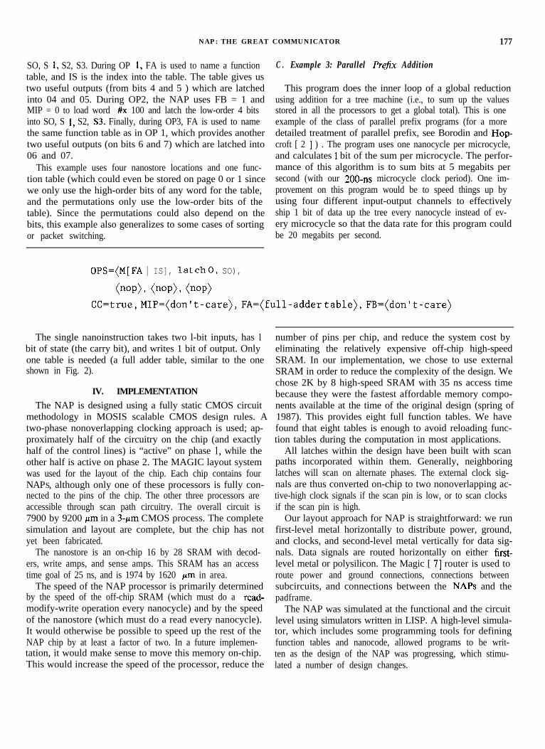
OPS=(M[FAII IS], latch0, SO),
(nap), (nap), (nap)CC=true,MIP=(don't-care),FA=(full-addertable),FB=(don't-care)
The single nanoinstruction takes two l-bit inputs, has 1bit of state (the carry bit), and writes 1 bit of output. Onlyone table is needed (a full adder table, similar to the oneshown in Fig. 2).
IV. IMPLEMENTATION
The NAP is designed using a fully static CMOS circuitmethodology in MOSIS scalable CMOS design rules. Atwo-phase nonoverlapping clocking approach is used; ap-proximately half of the circuitry on the chip (and exactlyhalf of the control lines) is “active” on phase 1, while theother half is active on phase 2. The MAGIC layout systemwas used for the layout of the chip. Each chip contains fourNAPS, although only one of these processors is fully con-nected to the pins of the chip. The other three processors areaccessible through scan path circuitry. The overall circuit is7900 by 9200 Frn in a 3-pm CMOS process. The completesimulation and layout are complete, but the chip has notyet been fabricated.
The nanostore is an on-chip 16 by 28 SRAM with decod-ers, write amps, and sense amps. This SRAM has an accesstime goal of 25 ns, and is 1974 by 1620 pm in area.
The speed of the NAP processor is primarily determinedby the speed of the off-chip SRAM (which must do a read-modify-write operation every nanocycle) and by the speedof the nanostore (which must do a read every nanocycle).It would otherwise be possible to speed up the rest of theNAP chip by at least a factor of two. In a future implemen-tation, it would make sense to move this memory on-chip.This would increase the speed of the processor, reduce the
number of pins per chip, and reduce the system cost byeliminating the relatively expensive off-chip high-speedSRAM. In our implementation, we chose to use externalSRAM in order to reduce the complexity of the design. Wechose 2K by 8 high-speed SRAM with 35 ns access timebecause they were the fastest affordable memory compo-nents available at the time of the original design (spring of1987). This provides eight full function tables. We havefound that eight tables is enough to avoid reloading func-tion tables during the computation in most applications.
All latches within the design have been built with scanpaths incorporated within them. Generally, neighboringlatches will scan on alternate phases. The external clock sig-nals are thus converted on-chip to two nonoverlapping ac-tive-high clock signals if the scan pin is low, or to scan clocksif the scan pin is high.
Our layout approach for NAP is straightforward: we runfirst-level metal horizontally to distribute power, ground,and clocks, and second-level metal vertically for data sig-nals. Data signals are routed horizontally on either first-level metal or polysilicon. The Magic [ 71 router is used toroute power and ground connections, connections betweensubcircuits, and connections between the NAPS and thepadframe.
The NAP was simulated at the functional and the circuitlevel using simulators written in LISP. A high-level simula-tor, which includes some programming tools for definingfunction tables and nanocode, allowed programs to be writ-ten as the design of the NAP was progressing, which stimu-lated a number of design changes.
178 KUSZMAUL AND FRIED
An RTLlike language was also constructed on top ofLISP; this language allows us to compose parts to makelarger parts, and to generate test vectors for ESIM, whichwe can use to drive the circuit extracted from the layout. Aregister transfer-level simulation was written in this lan-guage, which allowed the verification of individual cells andthe composition of cells, all the way up to a full chip-levelsimulation. The results of this simulation were comparedwith the results of ESIM simulations to verify the layout.The RTL simulator generates test vectors to drive ESIMand it generates a file which contains the outputs that ESIMshould generate if the layout is correct.
Although we have not implemented a controller, we be-lieve that the microcycle-nanocycle approach would sim-plify its design. This is because the microcontroller is re-quired to produce microinstructions at only 5 MHz (ratherthan at the 20-MHz nanocycle rate). The latency from themicrocontroller to the NAP chip is not critical.
V. EVALUATION AND CONCLUSIONS
We have shown that it is feasible to design a processorchip which supports a variety of bit-serial routing networksefficiently. This type of chip is a step toward understandinghow to build and operate interconnection networks formassively parallel computers. The NAP chip we have de-signed provides very flexible addressing mechanisms, andallows indirect addressing so that MAMD operation is pos-sible. This chip also supports three distinct means of multi-thread operation, so that different processors operating offthe same instruction stream can do different things. Finally,this processor chip has no ALU; table lookup is used for alloperations. We have found all of these mechanisms usefulin writing example programs, and believe that the NAP ap-proach can teach designers about how to provide addressingand processor selection mechanisms in SIMD processors,and about the issues involved in providing flexible and high-performance interconnection networks.
How well has the NAP design stood up to its original de-sign goals? Let us examine those goals one by one:
l Provide communications control which is as flexible aspossible. The operation of the processor is completely pro-grammable at both the microinstruction and the nanoin-struction level. Processors have considerable flexibility inaddressing modes, and indirect addressing at both the bitand the word level is well supported. In addition, there arethree distinct means for processors operating from the sameinstruction stream to do different things: in addition to thestandard conditional execution (which is made very generalin the NAP), they can have different nanoinstructions intheir nanostore, or use different operation tables in theirmemory. In practice, this allows programmers to write pro-grams with the simplicity implicit in SIMD control and syn-chronization, yet keep processors efficiently utilized doing
different things at the same time. Essentially, one can pro-gram a machine built of NAPS as sets of processors, even ifthose processors share the same microcontroller.
l Keep the input-output channels and memory as busyas possible performing useful work. Each microinstructionmay make up to four memory references, each of a read-modify-write nature. Every microinstruction executed bythe processor can be able to read from and write to up toeight input-output channels on the processor. All of the pro-grams written on NAP to date have been able to keep theinput-output channels active at least 1 bit per microcycle,which corresponds to our assumptions about wire latency.Similarly, most of these programs use most of the nano-cycles in a microcycle to perform useful work, so that mem-ory is well utilized. The cycle time of the NAP is also ingood agreement with the speed available from state-of-the-art commercial SRAMs or on-chip dRAM.
l The NAP should serve as a universal element for routingnetworks. To date, we have written NAP programs for mes-sage routing using algorithms designed for butterfly net-works [lo] using the same number of cycles as a node de-signed specifically for that purpose. We have also writtenNAP programs for parallel prefix [ 21 which execute in onemicrocycle per bit. Although these examples are not suffi-cient evidence to prove that NAP is in fact a universal com-munication element, they do indicate that NAPS would beuseful in a number of different networks.
l Experiment with an ALU-less processor. Our experi-ence in writing NAP programs using tables for operationsis that “compressed tables,” which do more than one thingin one operation, are immediately of use. For example, oneportion of the table might be used to increment a pointerwhile another part might perform a Boolean operation ona few bits from input channels. We had hoped that experi-menting with table-based operations might lead us to achoice of which operations to put into an ALU; instead, wediscovered that the generality offered by these tables wasjust the right thing for programming.
The assumptions that were used in designing the NAPsystem should be carefully examined. In particular, our mi-crocycle-nanocycle approach is implicitly based on the as-sumption that long-distance communication (e.g., betweenNAP chips) is much slower than short-distance communi-cation (e.g., between the NAP processor and the functiontable memory). This assumption may be incorrect. It is truethat the latency for long-distance communication is higherthan for short-distance communication, but research donesince the implementation of the NAP processor indicatesthat the clock rate for long wires might be substantially thesame as the clock rate for short wires [ 31. It may be difficultto use a NAP-like chip to effectively emulate special-pur-pose chips that treat their long-distance wires as transmis-sion lines.
NAP: THE GREAT COMMUNICATOR 179
We hope that the NAP chip will eventually serve as a test-bed for experimentation with new interconnection net-works and parallel algorithms. We plan to test the NAP de-sign using a variety of “benchmark” programs and net-works to test its utility as a general-purpose networkelement. Measurement of effect of indirect addressing andour processor differentiation mechanisms on processor uti-lization will tell us something about the efficiency of ourapproach. Finally, these mechanisms may lead to insightsabout how to write effective parallel programs for commu-nication networks.
ACKNOWLEDGMENTS
The authors thank Tom Cormen and Elliot Kolodner for their hardwork on the design, layout, and programming of the NAP; Bill Dally for hisdirection and feedback during the course of the NAP project; and CharlesLeiserson for his insightful comments, direction, and consultation in theearly stages of the NAP design.
REFERENCES
I. Bashe, C. J., Johnson, L. R., Palmer, J. H., and Pugh, E. W. IBM’sEarly Computers. MIT Press Series in the History of Computing,Cambridge, MA, 1986.
2. Borodin, A., and Hopcroft, J. E. Routing, merging, and sorting onparallel models of computation. In Proc. 14th Annual ACM Sympo-sium on the Theory of Computing, 1982, pp. 338-344.
3. Knight, T., et al. Self terminating low voltage swing CMOS outputdriver. In Proc. Custom Integrated Circuits Conference, 1987.
4. Greenberg, R. I., and Leiserson, C. E. Randomized routing on fat-trees. In Proc. 26th Annual IEEE Symposium on the Foundations ofComputerScience, Nov. 1985.
5. Hillis, W. D. The Connection Machine. MIT Press, Cambridge, MA,1985.
6. Leiserson, C. E. Fat-trees: Universal networks for hardware-efficientsupercomputing. IEEE Trans. Comput. C-34,10 (Oct. 1985).
7. Osterhout, J. K. Mugic User’s Manual. U.C. Berkeley, Berkeley, CA,1986.
8. Pippenger, N. Parallel communication with limited buffers. In Proc.25th Annual IEEE Symposium on the Foundations of Computer Sci-ence, Oct. 1984.
9. Private correspondence. Ferroxcube/Amperex Electronic Corp.10. Ranade, A. G. How to emulate shared memory. In Proc. 28th Annual
IEEE Symposium on the Foundations of Computer Science, Oct.1987, pp. 185-194.
1 I. Toffoli, T., and Margolus, N. Cellular Autonoma Machines. MITPress. Cambridge, MA, 1987.
12. Valiant, L. G., and Brebner, G. J. Universal schemes for parallel com-munication. In Proc. 13th Annual ACM Symposium on the Theory ofComputing, May 198 I.
BRADLEY C. KUSZMAUL received two S.B. degrees (in mathematicsand in computer science and engineering) from MIT in 1984. He receiveda S.M. degree in computer science from MIT in 1986, and is now a Ph.D.candidate in the MIT Department of Electrical Engineering and ComputerScience. His research interests include all aspects of parallel computing,including processor architecture, interconnection networks, algorithms,and programming methodologies. He worked on interconnection net-works and parallel processing at Thinking Machines, in Cambridge, Mas-sachusetts, during the summers of 1984 through 1987, and worked full-time at Thinking Machines during the 1987-1988 academic year. He is amember of ACM and IEEE.
JEFF FRIED is a founder and director of hardware development forConnect Telemanagement Systems Corp. From 1983 to I989 he worked atGTE Laboratories, where his research on advanced switching architecturesincluded building prototypes of broadband switches and developing sys-tem-level modeling and analysis tools. He received the B.S., M.S., and E.E.degrees from MIT, where he is a Ph.D. candidate in the Department ofElectrical Engineering and Computer Science. His research interests in-clude computer and telecommunication system architecture, VLSI andWSI design, optical interconnects, and parallel and distributed algorithms.He is a member of the ACM, IEEE, SPIE, and SIAM, has published over25 technical papers, and holds three patents.
Received February 1, 1989; revised July I, I989