nanotechnology the biggest science and engineering initiative since the apollo program
TRANSCRIPT

NanotechnologyThe biggest science and
engineering initiative since the Apollo program

Objectives
• 1. Make sense of Nanotechnology 2. Understand the smallness of nanoscale 3. Appreciate the impossibility of creating nanoscale materials with macroscale tools 4. Explore the applications of nanotechnology and how it is changing materials

What is Nanotechnology
nano.gov
Click on Tee-shirt

How small are nanostructures?
Single Hair
Width = 0.1 mm
= 100 micrometers
= 100,000 nanometers !
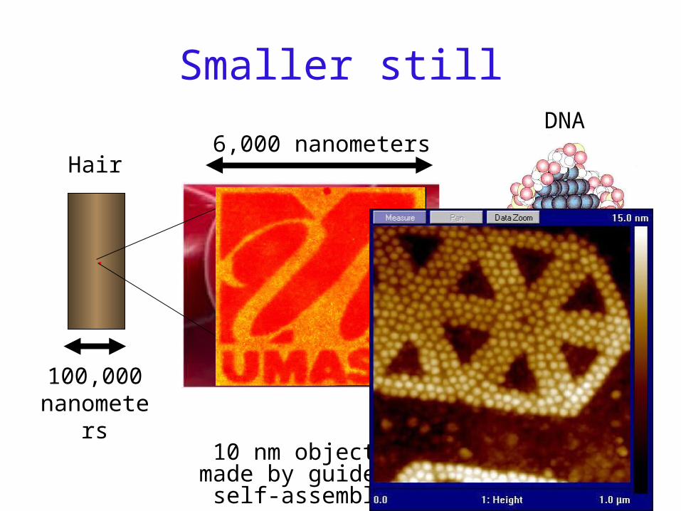
Smaller still
Hair
.
DNA
3 nanometers
6,000 nanometers
100,000 nanomete
rs10 nm objectsmade by guidedself-assembly

Applications of Nanotechnology

10 GB2001
20 GB2002
40 GB2004
80 GB2006
160 GB2007
First, An Example: iPod Data Storage Capacity
Hard driveMagnetic data storage
Uses nanotechnology!
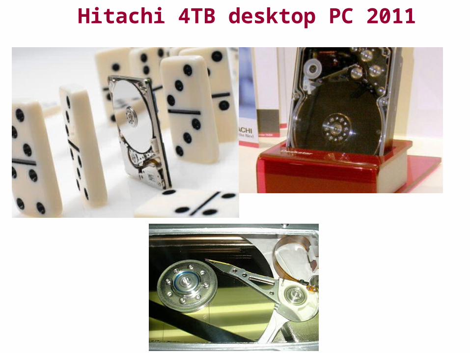
Hitachi 4TB desktop PC 2011
Why do we want to make things at the nanoscale?
• To make better products: smaller, cheaper, faster and more effective. (Electronics, catalysts, water purification, solar cells, coatings, medical diagnostics & therapy, and more)
• To introduce completely new physical phenomena to science and technology. (Quantum behavior and other effects.)
For a sustainable future!


Types of Nanostructuresand How They Are Made

"Nanostructures"
Nano-objects Nanostructured Materials
nanoscale outer dimensions
nanoscale internal structure
Nanoscale Devices and SystemsIntegrated nano-objects and materials
"nanoparticle""nanorod"
"nanofilm"
"nanotube"and more

Making Nanostructures: Nanomanufacturing
"Top down" versus "bottom up" methods
•Lithography•Deposition•Etching•Machining
•Chemical•Self-Assembly

Nanofilms
Gold-coated plastic for insulation purposes
"Low-E" windows: a thin metal layer on glass: blocks UV and IR light
Nanofilm on plasticNanofilm on glass

Photolithography
substrate
process recipe
spin on resist
resist
expose
mask (reticle)
develop
deposit
apply spin bake
spin coating
exposed unexposed
"scission"
liftoff
etch
narrow line
narrow trench
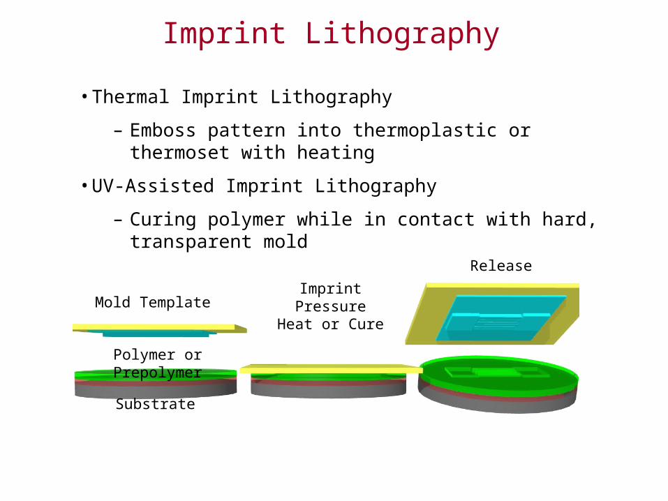
Imprint Lithography
Mold Template
Polymer or Prepolymer
Substrate
ImprintPressure
Heat or Cure
Release
• Thermal Imprint Lithography
– Emboss pattern into thermoplastic or thermoset with heating
• UV-Assisted Imprint Lithography
– Curing polymer while in contact with hard, transparent mold
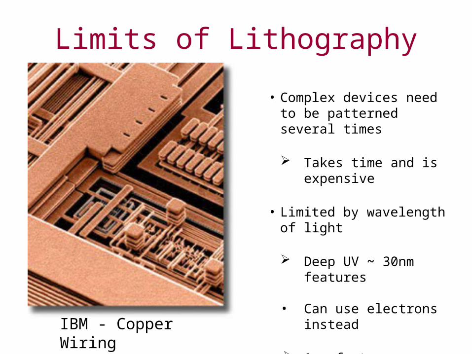
Limits of Lithography
• Complex devices need to be patterned several times
Takes time and is expensive
• Limited by wavelength of light
Deep UV ~ 30nm features
• Can use electrons instead
1nm features possible
MUCH slower than optical
IBM - Copper WiringOn a Computer Chip

Self Assembly

SELF ASSEMBLY with DIBLOCK COPOLYMERS
Block “A” Block “B”
10% A 30% A 50% A 70% A 90% A
~10 nm
Ordered Phases
PMMA PS
Scale set by molecular size

CORE CONCEPT FOR NANOFABRICATION Deposition
Template
EtchingMask
NanoporousMembrane
Remove polymerblock within cylinders(expose and develop)
Versatile, self-assembling, nanoscale lithographic system
(physical orelectrochemical)

nanoporous template
Nanomagnets in a Self-Assembled Polymer Mask
1x10¹² magnets/in2
Data Storage......and More

More Applications of Nanotechnology
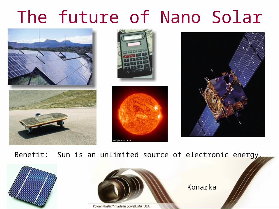
The future of Nano Solar
Konarka
Benefit: Sun is an unlimited source of electronic energy.
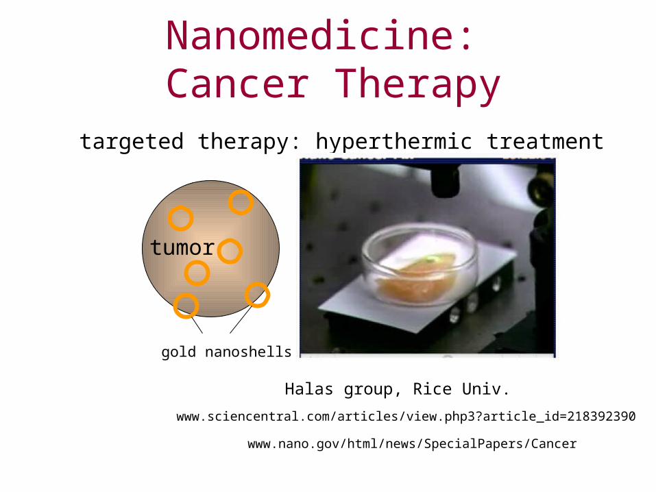
Nanomedicine: Cancer Therapy
tumor
gold nanoshells
Halas group, Rice Univ.
www.sciencentral.com/articles/view.php3?article_id=218392390
targeted therapy: hyperthermic treatment
www.nano.gov/html/news/SpecialPapers/Cancer

Perhaps the most important result in nanotechology so far: People from diverse fields working together to solve important
problems in our society
• Physics• Chemistry• Biology• Materials Science• Polymer Science• Electrical Engineering• Chemical Engineering• Mechanical Engineering• Medicine• And others
• Electronics• Materials• Health/Biotech• Chemical• Environmental• Energy• Food• Aerospace• Automotive• Security• Forest products

A Message for Students
Nanotechnology will change practically every part of our lives. It is a field for people who want to
solve technological challenges facing societies across the world
Some interesting ResourcesCA Berkely What is Nanotechnologyhttp://www.youtube.com/watch?v=4kHLj8la2Fo
Nano-waterproofing lesson