nanotechnology lsi url - dspace.jaist.ac.jp
TRANSCRIPT

Japan Advanced Institute of Science and Technology
JAIST Repositoryhttps://dspace.jaist.ac.jp/
Title極微細LSIのタイミング設計 : Timing Issues in
Nanotechnology LSI
Author(s) 金子, 峰雄
Citation
Issue Date 2007-03-07
Type Presentation
Text version publisher
URL http://hdl.handle.net/10119/8303
Rights
Description
4th VERITE : JAIST/TRUST-AIST/CVS joint workshop
on VERIfication TEchnologyでの発表資料, 開催
:2007年3月6日~3月7日, 開催場所:北陸先端科学技
術大学院大学・知識講義棟2階中講義室

Timing Issues in Nanotechnology LSI
金子峰雄北陸先端科学技術大学院大学 情報科学研究科
極微細LSIのタイミング設計
Mineo KanekoInformation Science, JAIST

Minimum width 60nm
VLSI in the Year 2007
1cm
1cm
Clock frequency 3GHz
0.33ns
1mm
167m167m
Arranging 1mm φ wire in Baseball ground
]m[167]mm[1
]cm[1]nm[60=
Light propagates 10cmin 0.33ns.
]m[1.0])s[1033.0(])m[103( 98
=××× −

Moore's Law (Gordon E. Moore)Complexity grows double in every 18-24 months
"Cramming more components onto integrated circuits", Electronics Magazine 19 April 1965
History of IC = History of Shrinking
Shrink → High Space-Density → More Transistors in a chip Shrink → Improved Tr. performance → High Speed IC Further shrinking
→ Large propagation delay, Inaccuracy in delay estimation,Static and dynamic delay fluctuation

Electrical Aspect of VLSI
MOS Transistor
L
Wdox
Current I, Voltage V,Capacitance Cg
LWdCVLWdI
oxg
ox
⋅⋅∝⋅⋅⋅∝
−
−−
1
211
Switching delay; delay
12211
1−
−−
−
⋅=⋅⋅⋅⋅⋅⋅
=⋅
∝ VLVLWdVLWd
IVC
delayox
oxg
Wire
L
HW
dOX
Resistance Rw,Capacitance Cw
1
11
−
−−
⋅⋅∝⋅⋅∝
OXW
W
dLWCWHLR
I
I
OXWW
W
dWHLWRC
IVCdelay
⋅⋅⋅
=⋅=⋅
∝2
Propagation delay; delay

L1, W1, dox1 L2, W2, dox2Lr, Wr, Hr, dOXr
Delay = Switching delay + Propagation delay
Elmore delay(First Moment Model)
Difficulty in delay estimation: Need higher-order modelVarious parasitic effects Static/Dynamic delay fluctuation
Static/Dynamic delay fluctuation: Fluctuations of chemical density and physical size in the fabrication processNoise on supply voltageCross-talk noise
( )
Electrical Aspect of VLSI
⎟⎟⎠
⎞⎜⎜⎝
⎛++
⋅+
= −−
−
−−
221
2
1
11
1
1221
21
2LWdLWd
HWL
VWdLLWdLWddelay ox
rrOXr
rr
r
ox
oxrrOXr κλ
Propagation delay is not improved by shrinking

Mask pattern
Specification
x
y
Physical-Level Design Transistor circuitModule generation Mask pattern design
Top-down Hierarchical Design of VLSI
Data flowControl flow
Algorithm-Level Design
Two-stage, Multi-stageState assignment Technology mapping
Logic-Level Design
Register Transfer-Level Design
Scheduling Binding Bus, multiplexer, net
t
System-Level Design HW/SW partitioningMemory architecture
MV Q

Timing issues in Data-path Execution of c = a + b
R1
FU1
R2
R3
Register
Functional unit
Register R1
Input of FU
Register R3
Output of FU
Control signal to latch a, b
time
Functional delay+ Propagation delay
arrival of the result c
Control signal to latch c
Timing of control signals ( , ) determines data-path behavior・ Many operations share the same FU, many data share the same register. ・ Various different delay values・ Delay may vary from its nominal value statically and dynamically.

Register R1
Input of FU
Register R3
Output of FU
time
Functional delay+ Propagation delay
ー Synchronous Systemー
Clock signal
・ Design needs ``Delay estimation'' + ``Timing margin'' ・ Easy to implement as a circuit・ Worst-case estimation + Sufficient margin = Low performance
Arrival of the result
R1
FU1
R2
R3
Register
Functional unit
Timing issues in Data-path

Register R1
Register R3
Output of FU
Input of FU
time
Detect the arrival of the result c
ー Asynchronous System ー
Send out latch control signal
Controller
・ No delay-estimation, no timing-margin ・ Tolerance to a large range of delay fluctuation ・ Large area (circuit) overhead in detecting-circuitry
R1
FU1
R2
R3
Register
Functional unit
Timing issues in Data-path
Functional delay + Propagation delay

R1
R2
R3
FU1
FU2
Data-path part+Control part
Resource Binding;assigns each operation to one of available functional units, and assigns each data to one of available registers
Scheduling;determines the start time of each operation
What is High-Level Synthesis?
u
v w
y
dxdu
x
dv dw
FU1
FU2
R1
R2
R3
time
u
wv
yx
Behavioral description of an application
algorithm

Layout(Floorplan)
ConnectionDelay information
Timing constraints
Wire-delay aware high-level synthesis:
SchedulingResource bindingConstraints on
parallel execution
Constraints on resource sharing
High-level synthesis under FU-delay dominant situation
A. New Approach to High-Level Synthesis

A. New Approach to High-Level Synthesis
Scheduling-Centric
Scheduling
Binding
Layout
Delay Extract
Evaluation
Binding-Centric
Binding
Layout
Delay Extract
Scheduling
Evaluation
3D-Approach
Binding
LayoutScheduling
Evaluation
Delay Extract
Wire-delay aware high-level synthesis:

A. 3D-Approach High-Level Synthesis
Execution Reconfiguration of a FU
Data lifetime Reconfiguration of a register
Application to Dynamically Reconfigurable LSI

Computation algorithm to be implemented (Dependence Graph) O, D :Set of operations,and set of data A : Dependency e : O → N ; Operation delay Sizes of functional units and registers
x
yt
( ) ix wip +( )ipx
( )ipy
( ) iy hip + ( )iσ
( ) ei +σ
( ) ( ) ( )( )( ) ( ) ( ) NiNipNip
iipip
yx
yx
∈∈∈ σ
σ
,,
,,dataoperation/each For
Need to check conflictsNeed to check timing constraints
( )ADODG ,,=
Naive solution space ( )DON +3
Execution or data lifetime
A. 3D-Approach High-Level Synthesis

x
yt
( ) ix wip +( )ipx
( )ipy
( ) iy hip + ( )iσ
( ) ei +σ
Execution or data lifetime
・ Each of Γ1, Γ2, Γ3, Γ4 is apermutation of elements in O,D
・ Γ5 is a permutation of elements in O (a topological order w.r.t. DG)
・ (Γ1, Γ2, Γ3, Γ4, Γ5) represents relative spatial relation in x-y-t space.・ O((|O|+|D|)^2) computation-time algorithm to compute
which has the minimum layout area and the minimum makespan among all solutions satisfying the spatial relation specified by the code.
・ The size of the solution space
Constrained Sequence-Quintuple
5-tuple (Γ1, Γ2, Γ3, Γ4, Γ5)
( )( )5!DO +
( ) ( ) ( )( ){ }DOiiipip yx U∈|,, σ
A. 3D-Approach High-Level Synthesis

A. New Approach to High-Level Synthesis
Basic Theory
Elementary Technology
・ Condition for feasible binding ・ Efficient solution space for 3D-Approach to High-Level
Synthesis
・ Binding constrained scheduling ・ Data-path layout, performance estimation
Synthesis System ・ Synthesis system considering wire delay ・ Synthesis system for reconfigurable systems ・ Synthesis system considering control skew ・ Synthesis system for asynchronous systems

B. Design Considering Skew
clock
R1
FU1
R2
R3
Register
Functional unit
R1
R3
clock
R1
R3
R1
R3
Max. delayMin. delay
Skew (timing difference)

B. Schedule and Skew Optimization
Optimum schedule under zero-skew
Minimum clock period=8Schedule length=3Total computation time = 8×3+0 = 24
8
6 8
36
4
R1
R2
R3
Applying skew optimization→skew values
Minimum clock period=7Schedule length=3Total computation time =7×3+1=22
)1,1,0(),,( 321−=rrr τττ
8
6 8
36
4
R1
R2
R3
Simultaneous schedule and skew optimization→skew value
Minimum clock period=5Schedule length=3Total computation time=5×3+3=18
)3,1,0(),,( 321=rrr τττ
8
6 8
3 6
4
R1
R2
R3
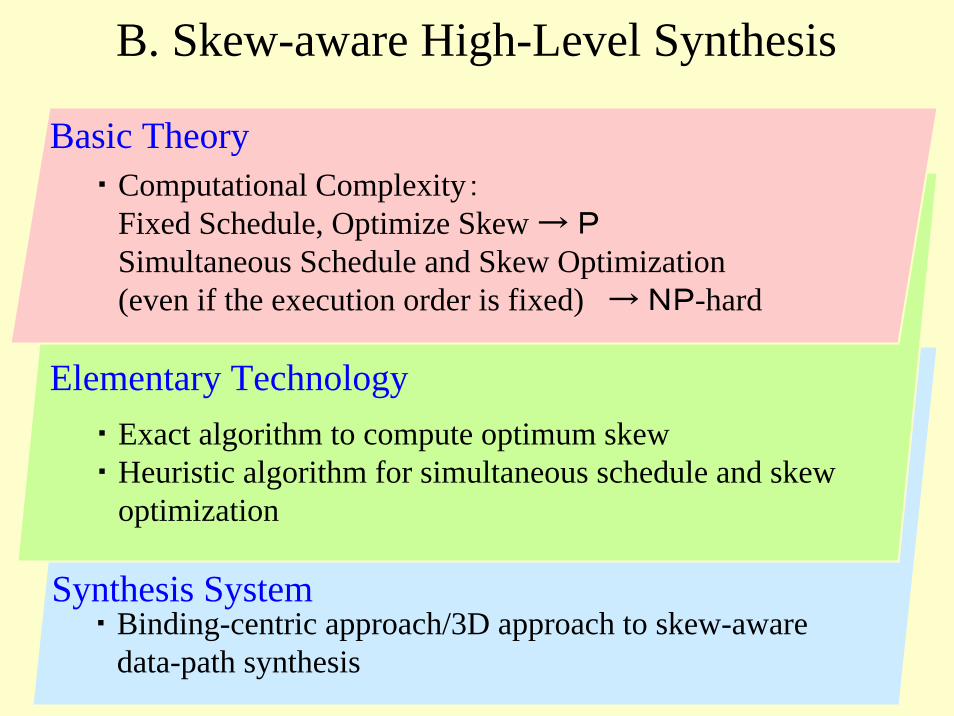
B. Skew-aware High-Level Synthesis
Basic Theory
Elementary Technology
・ Computational Complexity:Fixed Schedule, Optimize Skew → PSimultaneous Schedule and Skew Optimization (even if the execution order is fixed) → NP-hard
・ Exact algorithm to compute optimum skew ・ Heuristic algorithm for simultaneous schedule and skew
optimization
Synthesis System ・ Binding-centric approach/3D approach to skew-aware
data-path synthesis

C. Delay Fluctuation
clock
R1
FU1
R2
R3
Register
Function unit
R1
R3
Max. delayMin. delay
R1
R3 Violation of hold condition
R1
R3 Violation of setup condition
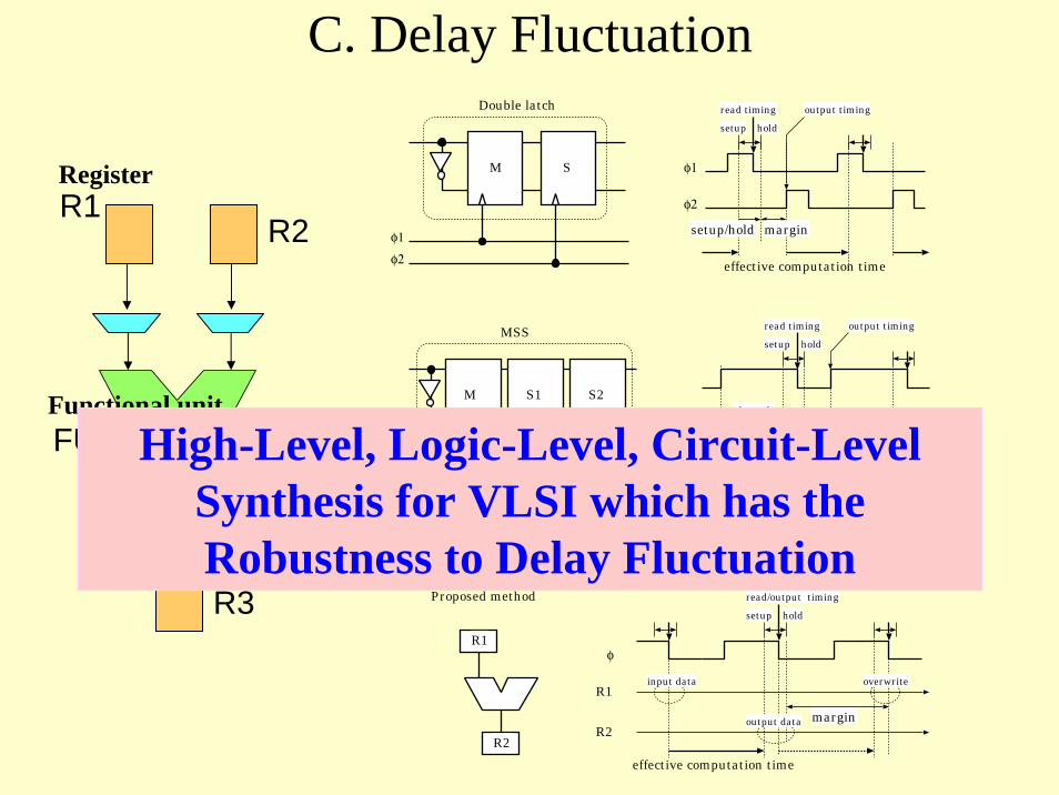
C. Delay Fluctuation
R1
FU1
R2
R3
Register
Functional unit
Double latch
φ1
φ2
φ1
φ2
effective computation time
φ
φ
MSS
M S1 S2M
S1
S2
marginsetup/hold
Proposed method
R1
R2
effective computation time
marginsetup/hold
effective computation time
margin
through
M S
R1
R2
input data
output data
overwrite
output timing
setup hold
read timing
setup hold
read timing output timing
setup hold
read/output timing
High-Level, Logic-Level, Circuit-LevelSynthesis for VLSI which has the Robustness to Delay Fluctuation

D. Asynchronous System
R1
FU1
R2
R3
Register
Functional unit
Max. delay R1
R3
Min. delay
Detect the output arrival
Detect the latch completion Send out latch control signal
Send out latch control signal
Controller
R1
R3
Controller
Setup and hold conditions are always satisfied.

o1 o2 o3o4
d3d2
d1
FU_1FU_2
Reg_1Reg_2Reg_3
working phaseidle phase
d4
0 1 2 3 4 5 6 7 8 time9
c1
c2
c4
d5d6
o4
d7
c3
MUX
o1 o2 o3
d4
DEMUX
d1 d3 d2
Reg_5
C
C
Reg_1 Reg_2Reg_3
Reg_4 Reg_6
Datapath
Controller
datacontrol signal
FU_1FU_2
o1 o2 o3o4
High-Level, Logic-Level, Circuit-LevelSynthesis for Asynchronous System
D. Asynchronous System

High performance/Low power/Reliable System on Chip
High speed, low power・Propagation delay and power consumption on signal/clock wires・Static/dynamic delay fluctuation
Large scale, system on chip・Huge size of optimization problems
VLSI: a core device for reliable e-society
Efficient algorithms for huge size of problemsDesign methodologies to break through the design crisis
Reliable chip: VLSI test, fault-tolerance
Reliability
Reliable design: Reliable EDA tools, 100% automation
Considering layout in high-level designRobustness, tolerance, insensitiveness to delay fluctuation
・Complex design constraints, a large number of design variables・Increasing circuit complexity, low voltage, chemical/physical fluctuation