nanoscale ductile mode ultraprecision … · 2.5 diamond turning of soft and brittle materials ......
TRANSCRIPT

NANOSCALE DUCTILE MODE ULTRAPRECISION
CUTTING OF POTASSIUM DI HYDROGEN PHOSPHATE
Rajanish Javvaji (B.Tech, Kakatiya University, India)
A THESIS SUBMITTED FOR THE DEGREE OF
MASTER OF ENGINEERING
DEPARTMENT OF MECHANICAL ENGINEERING
NATIONAL UNIVERSITY OF SINGAPORE
2008
i
ACKNOWLEDGEMENTS
I would like to use this opportunity to express my sincere gratitude to my
supervisors, A/Prof. Seah Kar Heng and Prof. Li Xiaoping, for their help and
encouragement for this project work. I would also like to express my sincere thanks to
Prof. Mustaffizur Rahman for his support and motivation during the period.
I would also like to thank staff of Advanced Manufacturing Laboratory, the lab
officer Mr. Tan Choon Huat and professional officer Mr. Neo Ken Soon for their
valuable advices given during the experiments. I also thank lab technologist Mr. Nelson
Yeo Eng Huat for assisting in operating the Toshiba ultra precision machine for my
experiments throughout. I also thank Dr. Zheng Ziwen for supporting during the final
experiments.
Besides I would like to thank my friends Mr. K.V.R.Subrahmanyam, Mr. Woon
Keng Soon, and Mr. Minbo Cai for their constant motivation and support during the
studies. It is unforgettable spending times with them and other friends in the lab.
I am grateful to my friends Mr. Hari Kishore Anumola, Mr. Sreenivas
Punireddy, Mr. Vempati Sreenivas, Mr. Talasila Sateesh, Mr. T. Satya, Mr. K. Rajan, Mr.
V. Pardhasaradhi and other roommates for their support and help in times of need.
I would like to thank National University of Singapore (NUS) for their financial
support during my tenure as graduate student and for the wonderful working environment
without which the work would not have been possible.
I am highly indebted to my Parents for all their affection and support without
which I could not have completed this work successfully. Lastly and most importantly I
thank my Almighty helping me to complete the studies.

ii
CONTENTS
Acknowledgements……………………………………………………………………….i
Abstract…………………………………………………………………………………..iv
List of Figures……………………………………………………………………............v
List of Tables…………………………………………………………………………..viii
Chapter 1 Introduction………………………………………………….………………1
1.1 Motivation………………………………………………………………..........1
1.2 Objectives of this Research Work……………………………………………..3
1.3 Organization of the Thesis………………………………………………….....4
Chapter 2 Literature Review………….………………………………………………...5
2.1 Introduction……………………………………………………………………5
2.2 Ductile Regime machining of Brittle Materials……………………….. ……..6
2.3 Mechanisms of Ductile Regime Machining in literature……………………...8
2.4 Brittle-Ductile Transitions in the Machining of Brittle Materials….………..13
2.5 Diamond Turning of Soft and Brittle Materials……………………………...16
2.6 Work Material – Potassium Dihydrogen Phosphate…………………………17
2.6.1 Importance of Surface Integrity for KDP applications……….……18
2.6.2 Diamond Turning of KDP material………………………………..22
2.6.3 Importance of Dry Cutting of KDP………………………………..24
2.7 Conclusion…………………………………………………………………...25
Chapter 3 Experimental Setup Details………………………………………………..26
3.1 Introduction…………………………………………………………………..26
3.2 Approach of Cutting KDP…………………………………………………...26

iii
3.3 Machine Tools and Equipment used…………………………………………27
3.4 Tool Material………………………………………………………………...28
3.5 Work Material………………………………………………………………..29
3.6 Vacuum Setup Description…………………………………………………..29
3.6.1 Theoretical evaluation of chip velocity…………………………….30
3.6.2 Calculation of flow velocity, air flow, suction pressure…………...32
3.6.3 Vacuum Calculation Steps…………………………………………35
3.7 Experimental Procedure……………………………………………………...35
3.8 The Maximum Undeformed Chip Thickness………………………………..36
3.9 Measurement of Cutting Edge Radius……………………………………….37
3.10 Measurement of Surface Roughness……………………………………….40
3.11 Experimental Cutting Conditions…………………………………………..41
Chapter 4 Experimental Results……………………………………………………….42
4.1 Introduction…………………………………………………………………..42
4.2 Ductile Cutting of KDP……………………………………………………...42
4.3 Implementation of Vacuum Suction Technique for extraction of Chips…....46
4.3.1 Discussions…………….…………………………………………..50
4.4 Machined Work piece Surfaces……………………………………………...51
4.4.1 Discussions………………………………………………...56
Chapter 5 Conclusions………………………………………………………………….60
Chapter 6 References…………………………………...……………………………...62

iv
ABSTRACT
Nanoscale Ductile Mode Cutting by using single point diamond turning is an
alternative approach for finishing brittle materials without subsequent polishing. The
process of machining brittle materials where the material is removed plastically leaving a
crack free surface is called ductile cutting. The developments in applicability of this
technology on materials such as silicon and germanium which are used in semiconductor
field has led to use in different other fields. One such other field is nonlinear optics in
which materials used usually are soft and brittle. The importance of surface integrity
requirement on these materials led to applicability of nanoscale ductile cutting
technology. Potassium Di-hydrogen Phosphate (KDP) is one such type of nonlinear
optical brittle material. It is one unique and most widely used inorganic nonlinear crystal
for frequency conversion processes. The surface integrity is an important criterion for this
material in the applications and requires a surface finish less than 5nm Ra. Nanoscale
Ductile Cutting of this soft and brittle material is being attempted in this research work.
The main objective of this research work is to develop an alternative technology
in finishing of this material without subsequent polishing operation and post processing
achieving surface finish less than 5nm Ra. This work involved the overcoming of the
challenges encountered with this material before and during machining such as handling
of this material and removal of chip from work zone. The use of vacuum suction
technique for extraction of chips is proposed in this work in dry cutting conditions.
Key Words: Ductile mode; Potassium Di Hydrogen Phosphate (KDP); Nano-scale; Dry
cutting

v
LIST OF FIGURES
Figure 2.1 Mechanism of material removal involving extrusion of heavily deformed
material ahead of a large radius tool in grinding of ductile metals………………………..9
Figure 2.2 Mechanism of material removal in grinding with machining with high
negative rake tools………………………………………………………………………...9
Figure 2.3 Schematic showing various stages of indentation……………………………10
Figure 2.4 Model of elastic-plastic indentation of brittle materials……………………...11
Figure 2.5 A model of chip removal with a size effect in terms of defects distribution…12
Figure 2.6 A projection of machining cut perpendicular to the cutting direction………..14
Figure 2.7 Structure of KDP crystal: (a) Projection along the a-axis and (b) Projection
along the c-axis…………………………………………………………………………..20
Figure 2.8 Frequency conversion process……………………………………………….21
Figure 3.1 Toshiba ULG-100C ultra precision machine………………………………...28
Figure 3.2 Picture showing single point diamond insert………………………………...28
Figure 3.3 Single crystal potassium di hydrogen (KDP)………………………………...29
Figure 3.4 Principle of operation of venturi suction nozzle……………………………..30
Figure 3.5 Merchant’s circle of cutting forces…………………………………………..32
Figure 3.6 Analogy showing venturi extraction of chips………………………………..34
Figure 3.7 Venturi vacuum setup and nozzle near work zone…………………………..35
Figure 3.8 Picture showing work piece setup…………………………………………...36
Figure 3.9 Schematic diagrams of maximum undeformed chip thickness……………...37
Figure 3.10 Fitting a circle to three points………………………………………………38
Figure 3.11 Picture showing atomic force microscope………………………………….40

vi
Figure 4.1 a and b Pictures of machined surfaces with the chips………………………..44
Figure 4.2 Nomarski surface without implementation of the vacuum at Dmax 24.85 nm..48
Figure 4.3 Nomarski surface with implementation of the vacuum at Dmax 24.85 nm…..49
Figure 4.4 Nomarski surface without implementation of the vacuum at Dmax 20 nm…...49
Figure 4.5 Nomarski surface with implementation of the vacuum at Dmax 20 nm……....49
Figure 4.6.a Fracture free surface at doc 80nm f 2µm/rev R 2mm Dmax 17 nm…………51
Figure 4.6.b Fracture free surface at doc 80nm f 2µm/rev R 2mm Dmax 17 nm…………51
Figure 4.7.a Fracture free surface at doc 100nm f 2µm/rev Dmax 19 nm………………...52
Figure 4.7.b Fracture free surface at doc 100nm f 2µm/rev Dmax 19 nm………………..52
Figure 4.8.a Fracture free surface at doc 100nm f 1.5 µm/rev Dmax 20 nm……………...52
Figure 4.8.b Fracture free surface at doc 100nm f 1.5 µm/rev Dmax 20 nm……………...53
Figure 4.9.a Fracture free surface at doc 150nm f 1.5 µm/rev Dmax 24.85 nm…………..53
Figure 4.9.b Fracture free surface at doc 150nm f 1.5 µm/rev Dmax 24.85 nm…………..53
Figure 4.10 Continuous chips at Dmax 17nm observed under SEM……………………...54
Figure 4.11 Continuous chips at Dmax 19nm observed under SEM……………………...54
Figure 4.12 Continuous chips at Dmax 33.64nm observed under SEM…………………..54
Figure 4.13 AFM surface for doc 80nm f 2µm/rev R 2mm Dmax 17 nm………………...55
Figure 4.14 AFM surface for doc 100nm f 2µm/rev R 2mm Dmax 19 nm……………….55
Figure 4.15 AFM surface for doc 100nm f 1.5µm/rev R 1mm Dmax 20 nm…………….55
Figure 4.16 AFM surface for doc 150nm f 1.5µm/rev R 1mm Dmax 24.85 nm………….56
Figure 4.17 AFM surface for doc 200nm f 1.5µm/rev R 1mm Dmax 32.41 nm………….56
Figure 4.18 Marks on surface wider than feed rate marks……………………………….58
Figure 4.19 Surface showing marks equal to feed rate marks…………………………...58

vii
Figure 4.20 Maximum undeformed chip thickness vs surface roughness Ra …………...59

viii
LIST OF TABLES
Table 2.1 Properties of KDP……………………………………………………………..19
Table 3.1 Machining parameters…………………………………………………………41

1
CHAPTER 1
INTRODUCTION
1.1 Motivation
Precision machining is defined as a combination of the very hard and sharp edges
obtained from certain crystalline (usually diamond) tools with the extremely precise
machine tools. These precise machine tools are incorporated with liquid or gas bearings
and operate under closely controlled environmental conditions to produce finished optical
surfaces. The precision machining technology removes some of the difficulties in
forming optical surfaces encountered in conventional grinding and polishing, specifically,
for the family of materials, both physically and chemically compatible with diamond
tools. Because the diamond tools are so hard and sharp, they present essentially no
cutting edge contact area to the material being worked which results in very little tool
wear and tool force. This leads to the basic tenant of diamond turning which states that
the surface created in the work piece will be an exact replica of a combination of the
cutting tool shape and its tool path. The process is developed to minimize mechanical
material deformation and hence, results in both the specular finish and contour accuracy
sufficient for optical surfaces (Marvin J Weber, 1995).
The demand for high precision and high performance components in the fields of
Optics, Electronics, Semiconductors, etc has led to the development of new materials and
new processing technologies. The components in the applications require brittle materials
like Ceramics, Glasses, Silicon, etc to be used due to their high performance efficiency,
lightweight, temperature and dimensional stability though they have high brittleness.

Chapter 1: Introduction
2
(Ngoi B. K. A. and Sreejith P. S, 2000). The high brittleness, which makes these
materials difficult to be processed, has led to development of Ultra Precision
Technologies such as Diamond Turning and Grinding. Single Point Diamond Turning has
been used for ultra precision machining in a variety of ductile materials, polymers and
crystals. The machining technologies can also be used for the brittle materials at proper
cutting conditions without subsurface damage achieving nanometric surfaces (Puttick et
al, 1989). The technology can also be extended to other fields such as non linear optics in
which materials used are liquid crystals.
Potassium Dihydrogen Phosphate (KDP) is an inorganic non-linear optical crystal
material most widely used in the field of non-linear optics for frequency conversion
processes. The combination of softness and high brittleness characteristics of the material
imposes a challenging task during processing and handling. Further it is deliquescent,
fragile and hygroscopic which adds to the difficulty for machining (Baruch A. Fuchs et
al, 1986, Qiao Xu et al, 1999). It is of most important to achieve a very fine surface finish
and surface integrity on optical crystals such as KDP in this field and at the same time
free from sub-surface damage to withstand higher laser powers for longer times.
Currently polishing, grinding, lapping and magneto-rheological finishing methods
are used for such type of non linear crystals but these processes cause sub-surface
damage which leads to failure of the surface within shorter time (Baruch A. Fuchs et al,
1986, Hou Jing et al, 2006). Polishing is also not well enough understood or controlled to
result in a predetermined surface finish (Marvin J Weber). So, nanoscale ductile mode
cutting by single point diamond tool is believed to give higher surface finishes with good
surface properties for longer life of crystals. The stability of surface roughness obtained

Chapter 1: Introduction
3
by diamond turning is more than by other methods. The spatial versatility, geometric
predictability and inherent repeatability of CNC Ultra precision machines offer a unique
alternative for optical surface manufacturing.
In this regard, this research study aims for significant contribution to the field of
non linear optics for finishing KDP crystals by alternative technology, Single Point
Diamond Turning.
1.2 Objectives of this Research Work
The main objectives of this research work are
To establish a new technology of finishing, called ‘Nanomachining’ for soft and
brittle material, Potassium Dihydrogen Phosphate (KDP) by achieving optical surface
finish (Ra below 5nm) in the field of non-linear optical applications such as Optical
Modulators, Pockel’s Cell etc.
In order to achieve this objective the following is proposed.
To perform Ductile Cutting of KDP with the undeformed chip thickness less than
cutting edge radius and to establish an effective method to overcome the difficulty
of eliminating machined chips which is identified as a main challenge in
machining of KDP in dry cutting conditions
Chapter 1: Introduction
4
1.3 Organization of the Thesis
In the present work, an experimental investigation of nanoscale ductile mode
cutting of Potassium Dihydrogen Phosphate is performed. Chapter 1 describes about the
background of the research work along with its objective. Literature review about the
ductile mode cutting of brittle materials, details of work material (KDP) such as
properties, applications, etc is presented in chapter 2.
Chapter 3 describes experimental details and equipments carried out in this study.
In this chapter details about the approach of cutting, vacuum setup used in the
experiments are discussed. Experimental results pertaining to the nanoscale ductile
cutting of KDP are discussed in Chapter 4. The conclusions are presented in Chapter 5.

5
CHAPTER 2
LITERATURE REVIEW
2.1 Introduction
Brittle materials like Ceramics, Semiconductors, and Glasses etc which are
usually hard and with low fracture toughness are difficult for machining. Such brittle
materials can be deformed plastically when the depth of cut is below several tens of
nanometers i.e., these exhibit plastic deformation like ductile materials below minimum
cut chip thickness. This is known as ‘Ductile Regime Machining’. The present chapter
provides an overview of literature, in the areas of ductile mode machining of brittle
materials, characteristics of KDP material, applications and importance of surface
integrity of KDP and ductile cutting of KDP. The following topics relevant to the present
work are reviewed:
• Ductile regime machining of brittle materials
• Mechanisms of ductile regime machining in literature
• Brittle-ductile transitions in the machining of brittle materials
• Diamond turning of soft and brittle materials
• Characteristics of work material (KDP material)
• Importance of surface integrity for KDP applications
• Diamond turning of KDP material
• Importance of dry cutting of KDP

Chapter 2: Literature Review
6
2.2 Ductile Regime machining of Brittle Materials
The application of brittle materials such as Ceramics, Glasses, Silicon etc in
various fields such as Optics, Semiconductor etc has led to development of processing
technologies of these materials. The brittle materials are used due to their high
performance efficiency, light in weight, able to perform in extreme environments etc.
The processing technologies include Ultra Precision Grinding and Ultra Precision Single
Point Diamond Turning. The development of Ultra Precision machines with resolutions
at nanometric accuracy has led to possibility of finishing brittle materials in a ductile chip
removal way. A lot of research has been going on this ductile mode finishing technology
lately, in machining of new brittle materials and finding the mechanism of ductile mode
machining. A review of machining of brittle materials by ductile grinding and diamond
turning processes is presented here.
Several researchers have reported that machining of the brittle materials in ductile
mode conditions is possible. The literature showed various brittle materials like
Ceramics, Semiconductors, Glasses, etc have been cut in ductile conditions and showed
fracture free surfaces can be achieved. The possibility of grinding brittle materials in a
ductile manner was proposed by King and Tabor (1954), when it was noted that during
frictional wear of rock salts, although there was some cracking and surface
fragmentations, the dominant material removal process was plastic deformation of the
surface layers and not fracture. Huerta and Malkin (1976) showed first reproducible
evidence of grinding brittle glass work pieces with the improvements in precision
diamond grinding mechanisms at that time.

Chapter 2: Literature Review
7
Blake N Peter (1990), who studied the precision machining of germanium and
silicon using single-point diamond turning, pointed out that the critical chip thickness is
an important parameter, which governs the transition from plastic flow to fracture along
the tool nose. Puttick et al (1995) conducted the single point diamond turning using cut
depths of the order 100 nm and achieved a surface quality corresponding to that achieved
by optical polishing, Ra≈0.6 nm, but the subsurface damage also can be observed under
the condition of ductile regime machining. Nakasuji et al (1990) carried out single-point
diamond turning of silicon with a tool having a nose radius of 0.5-1 mm and a rake angle
varying from 0 to -250 and found a surface roughness of 0.04 µm. Shibata et al (1996)
experimented on silicon wafers with a single-point diamond tool of nose radius 0.8 mm
and a negative rake angle of 400. Fang and Venkatesh (1998) reported that for turned
silicon surfaces with roughness value of Ra=23.8 nm, mirror surfaces of 1 nm roughness
were achieved repeatedly by micro-cutting, where a depth of cut of 1 µm. Leung et al
(1998) carried out direct machining of silicon on a precision lathe to a finish of 2.86 nm
roughness and found that in order to produce a high quality surface, it’s necessary that the
machining process is in the ductile regime and the chip thickness must be less than the
critical value, which depends on the machining conditions.
Many other researchers (Beltrao et al., 1999; Bifano et al., 1991; Lawn et al.,
1994; Moriwaki et al., 1992; Morris et al., 1995; etc) reported ductile regime machining
of Si, Ge, Ceramics and Glasses etc with high quality surfaces without subsurface
damages. This indicates that the process of ductile chip formation may be independent of
the nature of the materials (e.g., brittle or ductile, hard or soft, crystalline or amorphous,
etc.).

Chapter 2: Literature Review
8
2.3 Mechanisms of Ductile Regime Machining in literature
As mentioned in last section, much work about ductile-regime machining of
brittle materials has been reported, but the nature of the brittle-ductile transition is not
clear. Systematical study on its machining mechanism and the technology is of
theoretical significance and practical value. Many researchers have been involved into
understanding the phenomena of brittle-ductile transition and revealing the mechanism.
Some initial work is briefly described here.
The basic mechanism of ductile machining of brittle materials can be studied by
assuming the cutting process to be as indentation and scratching processes, since cutting
takes place at sub-micron level where cutting edge radius of the tool plays an important
role. The literature review showed indentation studies and low speed scratching
experiments can be used to analyze the fundamental deformation and fracture process
that may occur during ductile grinding and diamond turning processes.
Shaw (1972) proposed a mechanism of material removal involving extrusion of
heavily deformed material ahead of a large radius tool in grinding of ductile metals (Fig.
2.1) and Komanduri (1971) proposed a mechanism likening the grinding process to
machining with high negative rake tools (Fig. 2.2). Puttick et al (1989) used similar
models to include the case of nanometric cutting of nominally brittle material, such as
silicon. They proposed that brittle materials may be machined in a ductile manner
provided that the depth of cut is restricted below a critical value for crack initiation
predicted by energy scaling. The ductile machining is just like the extrusion of plastic
materials ahead of the tool. Lawn and Evans, 1977; Lawn et al., 1980 showed the
mechanism of material removal by brittle mode can be obtained by comparing this

Chapter 2: Literature Review
9
process with indentation-sliding analysis (Fig. 2.3). The material removal takes place in
six stages. As shown in fig 2.3 the material under the indenter is initially subjected to
elastic deformation.
Figure 2.1: Mechanism of material removal involving extrusion of heavily deformed material ahead of a large radius tool in grinding of ductile metals.
Figure 2.2: Mechanism of material removal in grinding with machining with high negative rake tools.
There creates a small inelastic deformation zone due to high hydrostatic pressure below
the indenter; (b) a median vent is formed on a plane of symmetry containing the contact
axis at the elastic-plastic boundary; (c) further increase of load makes the median vent
stable; (d) the median vent begins to close as the load is removed; (e) the lateral vents are
Chip
Tool stagnation
point
-Ve Rake
Clearance angle
Workpiece
Tool
Undeformed Chip Thickness
Chip
Elastic-plastic boundary
Rake angle
Deformed chip thickness
Grit-tip radius
Abrasive grit

Chapter 2: Literature Review
10
formed as indenter removal goes on and spread out laterally on a plane closely parallel to
the specimen surface. Residual stresses are the main cause to form lateral cracks (f) as the
indenter is removed completely lateral vents continue to extend towards specimen surface
and may eventually lead to removal of material by chipping. In nanometric cutting of
brittle materials such as silicon using a single crystal diamond tool, this mode of material
removal must be avoided as much as possible to eliminate brittle fracture and consequent
micro-crack formation on or near the surface.
Figure 2.3: Schematic showing various stages of indentation.
It is well known that the extent of plastic deformation is determined by the
magnitude of the hydrostatic stress. Under high hydrostatic pressures brittle materials are
capable of ductile behavior (Bridgeman, 1953). Such a condition exists at light loads
under the indenter in indentation testing. Immediately below the indenter, the material is

Chapter 2: Literature Review
11
assumed to behave as a radially expanding core (‘hydrostatic core’) exerting uniform
hydrostatic pressure on its surroundings, encasing the core in an ideally ‘plastic region’.
Beyond the plastic region lies the ‘elastic matrix’ (Johnson, 1970). Fig 2.4 shows a model
for elastic-plastic indentation of brittle materials.
Figure 2.4: Model of elastic-plastic indentation of brittle materials.
A model for material removal without microfracture was developed by Lawn and
Evans (1977). It is based on a model in which the elastic-plastic field beneath the indenter
is resolved into elastic and residual components. Nakasuji et al. (1990) and Shimada et al.
(1995) proposed a possible material removal mechanism, which can be classified into
two modes when machining brittle materials. One is the process due to plastic
deformation in the slip direction on the characteristic slip plane and the other is due to
cleavage fracture on the characteristic cleavage plane. When the resolved shear stress τslip
in the slip direction on the slip plane exceeds a certain critical value τc inherent to the
work piece material, a plastic deformation occurs in a small stressed field in the cutting
region of a specified scale, which may correspond to the depth of cut, for example. On
the other hand, a cleavage occurs when the resolved tensile stress normal to the cleavage
plane σslip exceeds a certain critical value σc. The mode of material removal depends on
P = Applied Load
2a ‘Hydrostatic Core’
‘Plastic Zone’
Surrounding region ‘elastic matrix’
a = Radius of the core
Chapter 2: Literature Review
12
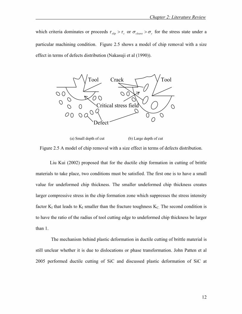
which criteria dominates or proceeds cslip ττ > or ccleave σσ > for the stress state under a
particular machining condition. Figure 2.5 shows a model of chip removal with a size
effect in terms of defects distribution (Nakasuji et al (1990)).
Crack Tool
Critical stress field
Tool
Defect
(a) Small depth of cut (b) Large depth of cut
Figure 2.5 A model of chip removal with a size effect in terms of defects distribution.
Liu Kui (2002) proposed that for the ductile chip formation in cutting of brittle
materials to take place, two conditions must be satisfied. The first one is to have a small
value for undeformed chip thickness. The smaller undeformed chip thickness creates
larger compressive stress in the chip formation zone which suppresses the stress intensity
factor KI that leads to KI smaller than the fracture toughness KC. The second condition is
to have the ratio of the radius of tool cutting edge to undeformed chip thickness be larger
than 1.
The mechanism behind plastic deformation in ductile cutting of brittle material is
still unclear whether it is due to dislocations or phase transformation. John Patten et al
2005 performed ductile cutting of SiC and discussed plastic deformation of SiC at

Chapter 2: Literature Review
13
nanoscale cutting is due to the high pressure phase transformation. They showed negative
rake angles and smaller depths of cut enhance the ductile machining characteristics.
2.4 Brittle-Ductile Transitions in the Machining of Brittle Materials
It is known that there is a transition in the material removal mechanism of brittle
materials from brittle to ductile mode when the depth of cut decreases. A lot of research
has been going on finding the brittle ductile transition for different materials.
Bifano et al (1991) investigated ductile-regime grinding and established a critical-
depth-cut model. Bifano postulated a basic hypothesis for ductile-regime grinding: all
materials, regardless of their hardness or brittleness, will undergo a transition from brittle
machining regime to a ductile machining regime if the grinding infeed rate is made small
enough. Below this threshold infeed rate, the energy required to propagate crack is larger
than the energy required for plastic yielding, so plastic yielding becomes the predominant
grinding mechanism. The critical-depth-cut model originates from a formula describing
the critical depth for fracture during indentation of hard materials and its formula to
predict the critical-depth-cut is:
2
⎟⎠⎞
⎜⎝⎛⎟⎠⎞
⎜⎝⎛=
HK
HEbd C
c
where CK is the fracture toughness and H is the hardness. E is the elastic modulus and
b is a constant which depends on the correlation between the calculated results and the
measured results. These relevant material property parameters are determined according
to the micro-indentation techniques. Consequently, as the scale of machining decreases,
plastic flow becomes an energetically more favorable material-removal mechanism. The

Chapter 2: Literature Review
14
critical depth at which a brittle-ductile transition occurs is a function of the intrinsic
material properties governing plastic deformation and fracture.
Blackley and Scattergood (1991) developed a new machining model for single
point diamond turning of brittle materials. Fig. 2.6 shows a projection of machining cut
perpendicular to the cutting direction.
Figure 2.6 A projection of machining cut perpendicular to the cutting direction.
According to the energy balance concept, fracture damage will initiate at the
effective cutting depth and will propagate to an average depth. The chip thickness varies
from zero at the tool center to a maximum at the top of the uncut shoulder as shown in
the figure. As long as the damage does not replicate beyond the cut surface plane, ductile
regime conditions are achieved. If the damage extends too deeply into the substrate, the
subsequent machining will not remove all the damaged material and indeed some damage
will remain in the finished work piece surface.
Nakasuji T and et al., 1990, discussed the importance of tool shape and cutting
conditions selection in ductile machining of Ge, Si and LiNbO3. The use of small nose
radius, small feed rate and small depth of cut creates small interference region and small
size of critical stress field. Ductile mode cutting can be achieved when tools of negative
Uncut Shoulder
f
dc = Critical Chip Thickness
Diamond Tool
Micro fracture Damage Zone
Cut surface plane
Tool center
Zeff
Damage transition line
yc

Chapter 2: Literature Review
15
rake angle are used even critical thicknesses of cut is large. They showed at identical feed
rate, surface roughness with the negative tool is better than the other. Blackley W. S. and
Scattergood R. O, 1991, showed theoretically that the larger nose radius is better in
ductile regime machining of brittle materials. They also showed large negative rake angle
gives beneficial effect on machinability in ductile regime as the critical depth of cut
parameter dc increases and it is negated by increase of damage depth yc. Maximum feed
fmax which indicates machinability increases significantly at large negative rakes. Lucca
D. A. et al, 1998, studied the effect of rake angle in orthogonal cutting of Ge over a range
of depths of cut below 500nm. They observed the cutting force and thrust force variation
and concluded that at lower depths of cut and higher negative rake angles the depth of cut
causing onset of significant surface fracture increases and increase in ratio of cutting
force to thrust force. And also direction of resultant force changes with lower doc and
higher negative rake angles which induces highest resolved shear stress along the
particular slip system.
However, Fang F. Z. and Zhang G. X, 2003, discussed the difference of cutting
mechanism with a 0o rake tool and an extreme negative rake tool. They showed
experimentally that effective rake angle plays an important role than nominal rake angle
in cutting of brittle materials. With an increase in cutting edge radius and a decrease in
undeformed chip thickness, the rake angle of the tool becomes more negative. The larger
negative rake tool produces more effective negative rake which creates more plowing and
sliding instead of chip formation. Ductile cutting can be achieved with a negative
effective rake angle cutting tool if the undeformed chip thickness is smaller than a critical
value even though 0o rake angle tool is used. Fang F. Z. and Venkatesh V. C, 1998 have

Chapter 2: Literature Review
16
shown zero rake gave better results than -25o rake angle since when -25o rake is used the
effective rake could be as high as -60o creating excessive pressure that could mar the
surface. They used 0.5mm nose radius tool explaining the difficulty of waviness control
of large nose radius when used.
2.5 Diamond Turning of Soft and Brittle Materials
As it is shown in the above section that all materials can be machined in ductile
mode but most of the work is being done on hard and brittle materials like Si, Ge, Glass,
Ceramics etc, a little work has been done on machining of soft and brittle materials.
Some researchers showed organic and inorganic nonlinear crystals which are soft and
brittle such as LiNbO3, L-arginine phosphate, KDP, CaF2 etc can also be diamond turned.
The works are discussed below.
Baruch A Fuchs et al (1989) showed L-arginine phosphate, an organic nonlinear
crystal can be diamond turned and discussed related issues like lubrication and cooling
during machining, effect of rake angle and crystal orientation on surface achieved. They
(1992) also performed diamond turning on Lithium Niobate in ductile shear mode and
discussed shoulder analysis technique and suggested more studies to ascertain the
optimum conditions for finishing on modern high precision lathe. Namba and Saeki
(2003) shown Thienylchalcone, an organic nonlinear crystal can be diamond turned and
studied effects of cutting direction and rake angle on surface roughness. Jiwang Yan et al
(2004) performed diamond turning on Calcium Flourde (CaF2) using straight edge tool
and studied effects of tool feed, rake angle, workpiece crystal orientation and cutting
fluid. Marsh R Eric (2005) reported a predictive model for surface figure extrapolated

Chapter 2: Literature Review
17
from force data in diamond turning of CaF2. Nakasuji (1990) turned Lithium Niobate
(LiNbO3) and showed it can be cut in ductile mode. The experimental results obtained in
ductile mode machining of commercial PZT (Piezoelectric transition) ceramics indicated
that the domain switching is associated with the ductile machinability with this group of
PZT ceramics (Beltrao et al, 1999).
2.6 Work Material – Potassium Dihydrogen Phosphate
Potassium Dihydrogen Phosphate (KDP) is an Inorganic dielectric nonlinear
material which is brittle and soft and also very thermally sensitive and hygroscopic. It is
widely used in nonlinear optical field for frequency conversion processes due to its high
laser damage threshold, high optical homogeneity, high structural perfection, high non-
linear efficiency and high transparency range (240-1600nm). KDP has low fracture
toughness and hardness which makes it difficult to machine, leading to application of
ductile regime machining at certain conditions for finishing of this material.
The combination of high brittleness with a relatively high coefficient of expansion
and low thermal conductivity of KDP makes it very vulnerable to breaking by thermal
shock (Richard C. Montesanti, 1995). So it is important to take utmost care while
processing this material. Some of the properties of KDP are shown in below in table 1.
KDP is a liquid crystal and grown from aqueous solution at rates of few mm/day.
Its melting point is only 2500 C and curie temperature is 122 K (-1510c). At room
temperature it is non-polar paraelectric and has a tetragonal crystal structure and it
changes to ferroelectric phase with ortho rhombic structure at 122 K (-1510c). The crystal
structure of KDP material is shown below in figure 2.2 (Yoshido H and et al, 2000).
Chapter 2: Literature Review
18
2.6.1 Importance of Surface Integrity for KDP applications
The definition of quality depends on the function that a work piece must perform.
The quality can refer to error in the Surface Contour, Surface Roughness of a work piece
and Sub surface damage which together is known as Surface Integrity. Surface Integrity
is defined broadly as the metallurgical and mechanical state of the machined surface.
Subsurface damage can be defined as any degrading effect that manifests itself just below
the surface of a work piece. Examples are residual stress, micro cracks that reside below
or extend from the surface into the bulk of the work piece, changes in the constitution of
the work piece near the surface such as hydration of glass, or change in the hardness due
to plastic working of the work piece material near the surface (Said Jahanmir et al 1999).
It is particularly the cracking that is so deleterious in machining of brittle materials such
as glass, ceramic etc. The absence of residual cracks extending into the surface which
degrade the breaking strength of a work piece is characteristic of ductile regime
machining such as grinding and single point diamond turning. The efficiency of the
nonlinear optical processes in which KDP is used depends on how good the optical
properties are achieved. These optical properties are dependent on the surface integrity of
the crystal. The applications of KDP material mainly are in Pockel’s Cell as Q-switches,
Optical Modulators and for Angle Tuning. Through nonlinear optics, laser radiation can
be converted from one frequency to another, significantly increasing the range of
applications that can be addressed.

Chapter 2: Literature Review
19
Properties of KDP
Crystal System(Space group)
Density (g/cm 3)
Hardness (kg/mm3)
Slip System
Solubility (oC) (g/100 g H2O)
Transmission (µm)
Refractive Index
Elastic Moduli (GPa)
Poisson’s Ratio
Melting Point
Heat Capacity (J/g K)
Thermal Expansion (10-6 K)
Thermal Conductivity(W/m K)
Elastic Constants @ RT
Cij (1011N/m2)
Tetragonal ( I -42m)
2.338
1.5(Mohs)
a. (101), (110), (112), (123)
<111>/2
b. (010) [100]
33 (25)
0.18-1.5
ne = 1.4669, no= 1.5074
E = 38, G = 15, B = 28
0.26
250oC
0.88
22.0║ a , 39.2 ║ c
2.0, 2.1
C11=0.7140, C12= -0.049,
C13=-0.020, C33=0.370,
C44=0.120, C66=0.07
Table 2.1 Properties of KDP.

Chapter 2: Literature Review
20
Figure 2.7 Structure of KDP crystal: (a) Projection along the a-axis and (b) Projection along the c-axis (Yoshido H et al, 2000).
In this nonlinear optical (NLO) interaction, one or two laser beams are directed into a
suitable material in which an output beam of the desired frequency is generated. NLO
interactions include harmonic generation, sum and difference frequency generation, and
parametric oscillation. The physics of an NLO interaction impose severe demands on
potential NLO materials. In general, a material must be optically transparent to the
incident and generated radiation, posses a quadratic susceptibility of sufficient
magnitude, allow for phase-matching of the interaction and withstand the laser intensity
without damaging. In addition to these, the material must have resistance against
photorefractive effects, should available in good quality, large size and with reasonable
price.
As a crystal, KDP is noted for its non-linear optical properties when compared to
other nonlinear materials. KDP when oriented properly is capable of converting a high
percentage of light at certain frequencies when passing through it to twice its incoming

Chapter 2: Literature Review
21
frequency. When certain frequencies of light are passed through consecutive crystals of
KDP and DKDP (Deuterium Potassium Dihydrogen Phosphate) that are properly aligned,
a large percentage of the incoming light may be converted to light of 3 times the
frequency as shown in fig. 2.8. KDP crystals are practically transparent in the visible and
near IR parts of the spectrum. It has high laser damage threshold, optical homogeneity,
high structural perfection, non-linear optical properties with high non-linear efficiency,
strongly birefringent (for phase matching), crystal symmetry and transparency over wide
range of spectrum with relatively low NLO coefficients. These are available in large,
homogenous pieces at relatively low cost. The hygroscopic property of KDP is the
drawback for the usage in some applications. The optical properties of KDP family of
crystals, higher damage threshold and ease of growth into large crystals make significant
in non-linear optics though they are hygroscopic.
Although the surface is coated with Anti-Reflecting (AR) coatings for higher
transference, a higher surface quality is important. The properties like high laser damage
threshold, higher transparency, high structural perfection depends on the processing of
the crystal material. The surface of the crystal material on which laser interacts should be
Figure 2.8 Frequency Conversion Process.
KDP
KDP
1064 nm 532 nm 355 nm

Chapter 2: Literature Review
22
free from sub-surface damage, scratches, residual stresses due to the finishing process,
without any contamination and should avoid any catastrophic failure. It has been
recognized that surface damage and surface plasma formation in optics under intense
illumination depends on the cleanliness and finish of their surfaces (Glass A. J et al.,
1972, Wood R.M. et al., 1975). A higher optical surface is achieved by proper finishing
technique. The higher surface finish requirement minimizes scatter losses and wave front
distortions while increasing the efficiency of optical systems.
A surface preparation process of a nonlinear crystal material starts with an as-cut
surface and progresses through a sequence of increasingly finer scale material removal.
In progressing through the sequence, it is of paramount important that each stage removes
all the damage, including especially sub-surface damage, introduced by the previous
stage. The cutting process for an NLO crystal should avoid catastrophic cracking due to
excessive mechanical or thermal stress (Peter F. Bordui and Martin M. Fejer., 1993). The
surface should be of high finish i.e., the surface roughness should be around λ/4 to λ/10
(λ – wavelength of laser used), higher flatness and good surface topography with
minimum waviness.
2.6.2 Diamond Turning of KDP material
KDP is a soft, brittle and fragile material which imposes a challenging task for
processing. In this section, literature review is presented on diamond turning of KDP
material.
A procedure for polishing the KDP family of crystals to high optical quality
surface finish and flatness is described by Sanjib Chatterjee (2005). The Ultra precision

Chapter 2: Literature Review
23
grinding of KDP crystal surfaces are reported by Namba Y and Katagiri M (1998).
Diamond turning in fly-cutting mode is performed on large KDP single crystals.
Researchers Baruch A. Fuchs and et al (1986) from LLNL developed a manufacturing
process using SPDT in fly cutting mode for large KDP crystals (100mmx100mm) and
concluded that smaller feed and larger tip radius of tool leads to more surface finish. Syn
Chol K and et al (1991) performed diamond turning of optical crystals and studied the
upper limit of the ductile cutting conditions by shoulder analysis technique and suggested
a systematic study on cutting of KDP by that technique on large KDP crystals (25 to 50
mm in diameter) and characterization of subsurface damage. Qiao Xu and et al (1999)
from Chengdu Fine Optical Engineering Research Centre, China explained the defects in
machining KDP surfaces and obtained surface roughness of 8 nm rms in their
experiments.
The researchers Chen M.J. and et al (2006, 2007) from Harbin Institute of
Technology, China have done work on brittle-ductile transition by indentation tests and
machining in fly cutting mode and evaluated theoretical equation for critical depth of cut
based on indentation principles and fracture mechanics. They stated tool’s geometry
parameter, feed rate and nominal depth of cut are main factors for surface quality of
KDP. The surface roughness achieved is more than 5nm Ra. Regression Analysis
technique has been used for prediction of surface roughness and cutting force by them.
The machining of KDP is performed by Japanese researcher Yoshiharu Namba (1998).
Indentation tests were conducted on KDP and DKDP by Tong Fang 2002 and
Kucheyev 2004 to find the micro-hardness and fracture toughness. Tong Fang 2002
described the properties elastic modulus (E) and fracture toughness (Kc) of KDP are

Chapter 2: Literature Review
24
anisotropic. Kucheyev 2004 mentioned low values of E and Kc should be taken into
consideration while processing this material.
The most of the work on SPDT of KDP has been done using Fly Cutting Mode
since the application for their requirements needs larger KDP crystals and these have
been machined using fly cutting mode. The size of crystals used depends upon the size of
the laser beam and the application in which it is used. Systematic studies on
machinability of KDP crystals can be performed for understanding various issues like
ductile mode cutting etc., by using relatively small crystals of size around 50x50mm
conveniently by SPDT in spiral cutting mode instead of fly cutting mode by using Ultra
precision machine.
2.6.3 Importance of Dry Cutting of KDP
From the literature studies it is found that several works have been done on
ductile mode cutting of hard and brittle materials like ceramics, glasses, quartz and
semiconductors, but a little work on soft and brittle materials like KDP. A very few
researchers have attempted to machine KDP material and shows comprehensive work
regarding the finishing of the KDP crystal material is necessary which plays an important
role in the field of non-linear optics. Moreover, it is reported surface roughness above
5nm which is not satisfactory for the non linear applications and the some literature
mostly discussed the procedure for machining and handling and cleaning of KDP.
KDP is susceptible to environmental degradation by moisture, oil residues, dust
etc due to its characteristic. The use of machining oil for flushing away chips causes
residual strains on the surface. The residual strains are removed by cleaning the crystal by

Chapter 2: Literature Review
25
solvents like toulene, xylene. The cleaning procedure causes ‘Fogging’ of the crystals
which is not required in the applications. KDP should be machined in dry cutting
conditions to avoid ‘Fogging’ of the crystal. In this regard, Dry cutting of KDP is
proposed in this research work. The main difficulty identified in dry machining of KDP is
chip removal from the machined surface. The machined chips produced are remained on
the surface causing damage. This problem is being dealt by proper technique in this
research work.
2.7 Conclusion
As it is discussed in the above sections, the research on ductile machining of KDP
is very less and also that little amount of work that has been done on ductile machining of
KDP reported surface roughness Ra more than 5 nm which is not sufficient in the
applications and machined in wet cutting conditions i.e., use of coolant. In this work, the
importance of dry cutting of KDP is emphasised and proposed in view of the
characteristics of this particular material.
The main challenge in dry cutting of KDP is chip elimination from work zone and
work surface. In this regard the objective of this research work is to establish proper
technique for elimination of chips from the surface. Vacuum extraction of chips from the
work zone using venturi is proposed in this work and shown that it is possible to
eliminate chips if the proper vacuum conditions are maintained. The following chapters
describe in detail about the experimental setup, challenges encountered and results.
In this regard, Nanoscale ductile mode cutting of KDP can be achieved by ductile
mode cutting by SPDT which provides an alternative technology for nonlinear optical
applications.

26
CHAPTER 3
EXPERIMENTAL SETUP DETAILS
3.1 Introduction
The details of machining approach of KDP, equipments and cutting tool are
discussed in this chapter. The experimental portion consists of face turning operation on
the KDP crystal. The maximum undeformed chip thickness equations used in the cutting
conditions and the method of measurement of cutting edge radius are briefly described.
Details of the vacuum setup used, theoretical analysis of vacuum parameters and the
machining parameters used in the experiments are also discussed.
3.2 Approach of Cutting KDP
It has been shown that tungsten carbide and silicon can be cut in ductile mode
under the set of conditions proposed by Liu Kui (2002). The proposed conditions are
1) smaller value of undeformed chip thickness and 2) values larger than 1 for the ratio of
cutting edge radius of the tool to maximum undeformed chip thickness should be used. It
is believed that the above conditions are suitable in achieving ductile cutting of KDP
material since this material is expected to have low value of critical chip thickness due to
its low fracture toughness and hardness values. The use of sharp diamond tools (cutting
edge radius 50 -100nm) and low undeformed chip thickness gives fracture free ductile
surfaces with minimum residual stresses. In the present work, ductile cutting of KDP
material is performed under the above conditions, which is different from the previous

Chapter 3: Experimental Setup Details
27
works in the machining of KDP. The studies are carried out in the dry cutting conditions
for achieving ductile crack free surfaces whereas the previous works used coolant.
3.3 Machine tools and Equipments used
The demand for use of Ultra Precision Machines in various applications such as
Optical components (sophisticated lens and mirrors), Fuel injection systems, etc is
increasing everyday since the finishing accuracy of the work piece greatly depends on
which it is machined. Ultra precision machines can be used for several materials and
produce surface accuracies at the order of nanometer for different components. For
getting good optical surfaces on KDP, the use of Ultra precision machine is very much
necessary. The spatial versatility, geometric predictability and inherent repeatability of
CNC Ultra precision machines offer a unique alternative for optical surface
manufacturing (Marvin J Weber, 1995). In this regard, face turning experiments were
carried out on Toshiba (ULG-100C) Ultra precision machine (Fig 3.1) having positioning
resolution of 1 nm. The maximum spindle speed and feed of this machine is 1500
revolutions per minute (rpm) and 450 mm/min respectively. The shock reservoirs are
attached with the machine to make it vibration free. The work piece is set on vacuum
chuck of the machine spindle.
Other equipments used in this research work are:
• Scanning Electron Microscope (SEM)(JEOL JSM-5500)
• Atomic Force Microscope (AFM) (SEIKO II SPA 500)
• Taylor Habson Surface Profilometer
• Nomarski Optical Microscope

Chapter 3: Experimental Setup Details
28
Figure 3.1: Toshiba ULG-100C ultra precision machine.
3.4 Tool Material
The tools used are single point diamond tools of 0.5mm, 1mm and 2 mm nose
radius. The cutting edge radii of these tools are around 50~80nm. The rake angle of the
tool used is 00. The clearance angle is 70. Figure 3.2 shows one of the diamond inserts
used in this experimental study.
Figure 3.2: Picture showing single point diamond insert.

Chapter 3: Experimental Setup Details
29
3.5 Work Material
Potassium Di hydrogen Phosphate (KDP) grown from liquid of size 60x60x15
mm3 is used for machining. The crystallographic orientation of the face machined which
is measured by X-ray Diffractometer is (001). Figure 3.3 shows the cubic single crystal of
KDP.
Figure 3.3 Single crystal potassium di hydrogen (KDP).
3.6 Vacuum Setup Description
In dry cutting of KDP, as it is identified during machining, the main challenge is
removal of chips from the work zone i.e., eliminating the chips from the work surface.
This is overcome by vacuum sucking device. For the purpose of chip extraction, it is
thought venturi vacuum pump is suitable as it is simple in operation and effective. The
other advantages of venturi system are compact and lightweight, can be positioned close
to the work zone, easily regulated, less maintenance, fast cycling and less expensive etc.
when compared to electro-mechanical pumps. The venturi works with the bernoulli’s
principle in which, when compressed air is passed through throat section, the velocity of
compressed air increases and pressure in the suction port decreases creating the pressure

Chapter 3: Experimental Setup Details
30
differences in suction port and atmosphere. Higher-pressure ambient air outside the
system flows in through channels in the generator, trying to create equilibrium. This
outside air mixes with high-speed air used to generate low pressure, and the combination
exits through the exhaust. With this method, the vacuum level depends on the nozzle.
There is a consistent relationship between pressure and velocity, with a high-velocity
fluid creating low pressure according to Bernoulli’s Principle. Fig. 3.4 shows the
principle of operation of venturi.
Figure 3.4 Principle of operation of venturi suction nozzle.
3.6.1 Theoretical evaluation of chip velocity
Ernst and Merchant orthogonal cutting theory is used in analyzing the chip
velocity. As KDP is cut in ductile conditions, continuous chips are produced, to which
this theory is used for chip velocity analysis.
Exhaust
Compressed Air Supply
Suction
Throat Section

Chapter 3: Experimental Setup Details
31
The basic mechanism in chip formation has been recognized as a shear process
taking place along a shear plane in the work material. By shearing action the work
material is plastically deformed and separated from the work piece. In Ernst and
Merchant analysis chip is assumed to behave as a rigid body held in equilibrium by the
action of the forces transmitted across the chip-tool interface and across the shear plane.
This is shown in below fig. 3.5. Their analysis is based on the idea that shear angle φ
would take a value such that work done is minimum. As for given cutting condition work
done is proportional to the cutting force Fc, Fc is expressed in terms of shear angle φ and
shear angle φ is obtained for which Fc is minimum (Geoffrey Boothroyd and Winston A
Knight).
From Merchant’s force diagram shown in figure 3.5,
C
C
NFTan == βµ -----------------------Eq. (3.1)
ααφ
rSinrCosTan−
=1
----------------------Eq. (3.2)
Where r is the chip thickness ratio
2
2 παβϕ =−+ -------------------------Eq. (3.3)

Chapter 3: Experimental Setup Details
32
Figure 3.5 Merchant’s circle of cutting forces.
The cutting velocity, v, is the velocity of the tool relative to the work piece. The
chip velocity vc is the velocity of the chip relative to the tool and is directed along the
tool face.
)(
.αϕ
φ−
=Cos
vSinvC -------------------------Eq. (3.4)
Here in this work above equation is used for calculation of chip velocity and the values of
α, φ and β are calculated accordingly from the above equations.
3.6.2 Calculation of flow velocity, air flow and suction pressure
Airflow is the amount or volume of air moving through the vacuum, usually
measured in Standard Cubic Feet per Minute (SCFM). The airflow (SCFM) into the
suction port should be more than the material removal rate (MRR). The velocity of the

Chapter 3: Experimental Setup Details
33
airflow is the speed of air at any given point in the vacuum system. It is measured in
metres per minute. Suction is the pull power that creates the velocity of airflow necessary
to move debris through the vacuum system. The stronger the suction power, the greater
the velocity of air flow. So suction power that creates higher velocity of air flow
(including with chips), is needed in the present case application. The smaller size of the
nozzle creates higher velocity of air particles at the entrance causing higher suction.
The performance of any venturi vacuum generator is defined by the following factors:
a. Supply Flow: Supply flow describes the flow consumption of the device. It is measured
in terms of SCFM (Standard Cubic Feet per Minute) of air consumption at various supply
pressures.
b. Flow Capacity: Flow capacity is a measure of free air (in SCFM) induced into the
vacuum port of the device when the vacuum port is open to atmosphere.
c. Vacuum Level: Vacuum level is a measure of the vacuum generated with the vacuum
port blocked off from atmosphere.
As it is discussed the air flow velocity (vcf) carrying the chips should be greater
than the chip velocity (vc) at which it comes out from work, Airflow (SCFM) is
calculated from the basic continuity equation that quantity of flow equals product of
velocity of flow multiplied by area of hose which is shown in below equation
Airflow (SCFM) = vcf X Area of hose or nozzle -----------Eq. (3.5)
The diameter of the venturi meter used is ¾” and size of the suction tube at the
work zone is ½”. The actual suction pressure required at the suction port of venturi is
calculated indirectly by deriving the equation for time required for evacuation.

Chapter 3: Experimental Setup Details
34
Consider a volume V of chips is to be evacuated per unit time with flow rate of air
Q by the suction port. The time required for evacuation of volume of chips can be
estimated by applying continuity equation. Below fig. 3.6 shows the V volume of chips,
Q flow rate of air and venturi.
The assumptions made in the above analysis are that flow of chips is steady and
rate of change of volume remains constant.
Figure 3.6 Analogy showing venturi extraction of chips.
Applying continuity equation the time required for evacuation can be derived in
terms of V, Q and atmospheric pressure P0 (psia) and suction pressure to be maintained in
the suction portion of the venturi P (in terms of psia).and it is shown below.
PP
InQVt o= --------------------Eq. (3.6)
From the above analysis, suction pressure required in the suction port of the
venturi can be found by volume V of material to be extracted per one sec. Fig. 3.7 shows
the venturi setup used and nozzle near work zone.
V
Q
venturi

Chapter 3: Experimental Setup Details
35
3.6.3 Vacuum Calculation Steps
a. Initially chip flow velocity (vcf) required is to be calculated from chip velocity (vc)
b. Diameter of venturi nozzle is ¾”
c. Calculate the material removal rate (v) from the cutting geometry and cutting speed
data.
d. Find Q suction flow of the air
e. Estimate the suction pressure to be reached in the suction port of the venturi sample
Figure 3.7 Venturi vacuum setup and nozzle near work zone.
3.7 Experimental Procedure
Face turning experiments are carried out on the work piece on Toshiba ULG 100
Ultra precision machine. KDP crystal is hand polished first to make smooth enough to be
able to glued on the aluminum block. This aluminum block with the square crystal is
vacuum chucked to the machine and then face turning operations are carried out. Fig. 3.8

Chapter 3: Experimental Setup Details
36
shows the crystal glued to the aluminum block. The gluing procedure and handling issues
of KDP crystal are discussed in the following chapter. The machining conditions are
followed such that the maximum undeformed chip thickness should be less than cutting
edge radius of the tool.
Figure 3.8 Picture showing work piece setup.
3.8 The Maximum Undeformed Chip Thickness
The maximum undeformed chip thickness, dmax, can be calculated from equations
below according to the cutting tool geometry and cutting conditions used in the
experiments. Fig 3.9 shows the schematic diagram of the maximum undeformed chip
thickness in the ultra-precision face turning experiments (Liu Kui, 2002). Here, a0 is the
depth of cut; R is the nose radius; O1 and O2 are the centers of two adjacent arc cutting
edges, and the distance between O1 and O2 is the feed rate, f used in the experiments.
The maximum undeformed chip thickness dmax for the condition faRa oo ≤− 22 as
shown in fig. 3.9 (a):
oad =max

Chapter 3: Experimental Setup Details
37
The maximum undeformed chip thickness dmax for the condition faRa oo >− 22 as
shown in fig. 3.9 (b):
222max 22 oo aRaffRRd −−+−=
(a) Feed rate quite large ( faRa oo ≤− 22 ) (b) feed rate quite small ( faRa oo >− 22 )
Figure 3.9 Schematic diagrams of maximum undeformed chip thickness.
As the feed rate used in the experiments is very small, second condition from
above satisfies the required conditions and it is used for calculation of maximum
undeformed chip thickness.
3.9 Measurement of Cutting Edge Radius
The cutting edge radius of sharp tool is below the optical diffraction limit and
hence it is very difficult to develop an effective yet simple measurement technique. It has
been reported that for freshly sharpened diamond tools, the cutting edge radius is
normally in between 20-70 nm (Komanduri et al. 1998). Therefore nano-precision
measurement of diamond cutting tools has become a key issue for ductile mode cutting of

Chapter 3: Experimental Setup Details
38
brittle materials. Many methods were proposed for measuring cutting edge radius of the
diamond tools. In this work, the method proposed by Li X. P. et al (2003) is used for
measuring. This method is a non-destructive in which the tool profile is indented onto the
copper block. This indented tool profile will be analysed using an AFM. The profile
curvature of indentation is copied, fitted to a circle and radius of the circle can be found
by simple mathematical analysis and Matlab. This is shown below.
Consider a set of three points P1(x1, y1), P2 (x2, y2) and P3(x3, y3) that lie along the
radius of the tool as shown figure 3.9. The line ‘a’ passes through the first two points P1
and P2. The line ‘b’ passes through the next two points P2 and P3.
Figure 3.10 Fitting a Circle to three points.
The equations of these two lines are
11 )( yxxmy aa +−= 22 )( yxxmy bb +−=
where ma and mb are the slopes of the two lines. The slopes are given by the following
equation
12
12
xxyyma −
−=
23
23
xxyy
mb −−
=

Chapter 3: Experimental Setup Details
39
The centre of the circle is the intersection of the two lines perpendicular to and passing
through the midpoints of the lines P1P2 and P2 P3. The perpendicular of a line with slope
m has slope -1/m, thus equations of the lines perpendicular to lines ‘a’ and ‘b’ and
passing through the midpoints of P1P2 and P2P3 are given by (3.33). These two lines
intersect at the centre of the circle and hence solving for x gives (3.34). The value of y
can be calculated by substituting the x value into one of the equations of the
perpendiculars. The radius is the distance between any one of the points, for example the
point P1 and the center.
.
2121*
221 yyxxx
my
aa
++⎟
⎠⎞
⎜⎝⎛ +
−−=
221 3232
* yyxxx
my
bb
++⎟
⎠⎞
⎜⎝⎛ +
−−=
( ) ( ) ( )( )ab
abba
mmxxmxxmyymm
x−
+−++−=
2322131
The computation described above was carried out in Matlab®. The radius of the circle
was affected by the choice of the three points along the profile of the tool. Hence a
number of different points were chosen from different profiles and an average value was
computed. As this measurement is not accurate enough because of some amount of spring
back in the copper material after the process of indentation, the measurements obtained
from the AFM are enlarged by a factor of 1.5.

Chapter 3: Experimental Setup Details
40
3.10 Measurement of Surface Roughness
The surface roughness analysis is performed by Atomic Force Microscope (AFM)
and Taylor Habson Profilometer. Atomic Force Microscope is widely used for surface
analysis which consists of scanning a sharp tip on the end of a flexible cantilever across a
sample surface while maintaining a small, constant force. AFM provides three-
dimensional surface topography at nanometer lateral and sub angstrom vertical resolution
on insulators and conductors. The tips typically have an end radius of 2nm to 20nm,
depending on tip type. Because of the high resolution, AFM has proved to be an excellent
method for process control and quality assurance in the applications where nanometer
accuracy is essential (Brinksmeier E et al 1998). Tapping mode is used for surface
roughness analysis as it avoids damage to the KDP machined surface. Average roughness
value Ra and other parameters are observed for different cutting conditions. Fig. 3.10
shows the Atomic Force Microscope (S.I.I. SPA-500) used.
Figure 3.11 Picture showing atomic force microscope.

Chapter 3: Experimental Setup Details
41
3.11 Experimental Cutting Conditions
The table below shows the final experimental conditions used, after preliminary
experiments for obtaining optical surfaces. The possibility of vacuum extraction of chips
is done with different cutting conditions in the preliminary experiments and the below
conditions are used for showing the results of vacuum system. The cutting edge radius of
1mm nose radius tool used is 57 nm and of 2mm tool is 81nm. The maximum
undeformed chip thickness (Dmax) is calculated as discussed previously. The spindle
speed is maintained at 1000rpm for all machining conditions. Smaller values of
undeformed chip thickness are obtained only when given depth of cut and feed rate
values are used and also to maintain the ratio of ratio of cutting edge of the tool to
maximum undeformed chip thickness used larger than 1, these given cutting conditions
are chosen.
S. No
Doc a0 (nm)
Feed rate (µm/rev)
Nose radius
(mm)
Dmax (nm)
1.
2.
3.
100
150
200
1.5
1.5
1.5
1 1 1
20.00
24.85
32.41
4.
5.
6.
80
100
300
2 2 2
2 2 2
17.00
19.00
33.64
Table 3.1 Machining parameters.

42
CHAPTER 4
EXPERIMENTAL RESULTS
4.1 Introduction
The higher surface finish requirement in the applications of KDP material can be
best achieved by Nanomachining by single point diamond tool in ductile mode. The
fracture free surface by ductile cutting can be useful for the nonlinear applications of
KDP. In this regard, machining experiments are conducted on KDP using the machining
conditions as shown in previous chapter. The challenges encountered during machining
of KDP are discussed in this chapter. The method to overcome chip removal by vacuum
suction is explained in this chapter and results are discussed. In this chapter, it is shown
that soft and brittle KDP material can be machined in ductile mode conditions at very
small undeformed chip thicknesses: showing the results of fracture free ductile surfaces,
chips and surface roughnesses obtained. The following sections show the above
mentioned.
4.2 Ductile Cutting of KDP
As discussed in the previous chapter, ductile mode cutting is performed under the
conditions that the undeformed chip thickness is less than the cutting edge radius and also
smaller undeformed chip thicknesses should be used. As it is mentioned before, the
difficulties processing this material are observed during the preliminary experiments
performed on the crystal.

Chapter 4: Experimental Results
43
KDP is very soft, fragile, deliquescent brittle material and also susceptible to
thermal variations which makes a different material from other brittle materials. The
characteristics makes difficult to process (handling and machining). It has to be carefully
handled and fixed onto the aluminum block which it is fixed to vacuum chuck for
turning. The crystal should be hot glued with glue’s melting temperature around 500 C; as
it introduces cracks in the crystal which leads to breakage of the crystal if it is around
1000 C. Therefore, rate of change of temperature experienced by the crystal must be low.
Here, soft gluing process is implemented to fix the work on aluminum block. KDP crystal
is glued on the aluminum block using araldite (soft glue) and this in turn is fixed on the
vacuum chuck of the machine. This issue of handling and fixturing makes a critical step
in machining of KDP crystals as proper care should be taken.
The main challenges encountered during machining of this material in dry cutting
conditions are chips staying at the work zone, on the machined surface and their removal.
These chips make damage to the machined surface. Below figs. 4.1 a and b shows
nomarski surfaces with the chips on the machined surface.
In macro machining one of the main issues is the entangling of the chips with the
tool and causing damage to the machined surface. This problem becomes severe in
micro/nanomachining. As micro/nanomachining is used mainly for higher optical
surfaces, even the small particle will scratch the newly machined surface. Chip removal,
therefore is to be carried out without causing the chips to remain on the work piece and
damaging the machined surface.

Chapter 4: Experimental Results
44
(a)
(b)
Figure 4.1 Pictures of machined surfaces with the chips.
This problem of chips is aggravated by the fact that the KDP material is very soft, and
degradable due to dust, etc., it is easily suspectible to damage. As machining is carried in
dry cutting conditions instead of use of machining oil to avoid fogging problem, a proper
technique is to be established for elimination of chips from the surface. So machining of
KDP in dry conditions makes a challenging task to remove chips. The probable reason
for chips stay on the surface could be the increase of cutting temperature which makes
the material soften since its melting temperature is 2500C. The generated cutting
temperature could be reason for chips glue on the machined surface.
Initially in this study various methods are tried to eliminate the chips from the
surface such as post cleaning process (blowing of air and drag wiping) and use of

Chapter 4: Experimental Results
45
different geometries of tools (various negative rake angle tools and nose radius tools).
This problem was attempted to solve by blowing air during the machining. The chips
were not removed by blowing air method further this caused sub-surface damage.
Another possible way to removal of chips is to clean the surface after machining with
proper solution by drag wiping technique which can be used with KDP material. Such
method also caused surface damage in the process and failure of the surface.
As the cutting is performed in dry cutting conditions, it is thought the elimination
of chips from the surface could be achieved by selecting appropriate tool geometry
(Nakayama K et al 1981), and cutting conditions. In this regard, experiments are carried
out with different tool geometries such as nose radius R (0.5 mm, 1 mm, 2 mm) and rake
angle (-50, -7.50, -100) with R 2mm. Although it is observed that at some conditions and
tool geometries, the chips can be eliminated from the surface, it is not repeatable and
reliable method of elimination of the chips from the work zone.
This problem of chips on the surface could be encountered by flushing of cutting
fluid during machining instead of dry machining. A proper cutting fluid (vegetable oil)
which is compatible with KDP material can be used. The use of cutting fluid reduces the
surface temperature and at the same time flushes away the chips giving fine surface with
no chips on the surface.
This problem of chips on the machined surface is not reported by any previous
researchers in machining of KDP. Researchers Baruch A. Fuchs and et al (1986) had
diamond turned KDP in fly-cutting mode using streaming cooling oil which maintained
uniform temperature at the cutting zone preventing re-crystallisation simultaneously
Chapter 4: Experimental Results
46
flushing away the chips. Researchers Chen M J and et al (2006, 2007) have also used
cooling oil.
However, if the coolant that is suitable with KDP material is used, it is to be
cleaned from the workpiece using solvents Toluene or Xylene (Baruch A. Fuchs and etal,
1986; Richard C. Montesanti, 1995). This may also cause surface fogging or
environmental degradation of the crystal surfaces by improper cleaning process. The
fogging problem of the crystal surfaces by usage of some turning oils is described by
Kozlwski M R and et al, 1991, which leads to the increase of surface roughness causing
increased beam modulation and scattering losses.
The solvents like Xylene and Toulene for cleaning machining oil from the crystal
must be used in special laboratory conditions since they are toxic. This procedure may
not be suitable for use in machining environment and also not suitable for practical
application of diamond turning of these KDP crystals.
Therefore, the use of vacuum system to suck the chips during the dry machining
is hence studied and applied to eliminate the chips forming on the machined surface.
4.3 Implementation of Vacuum Suction Technique for extraction of
Chips
The problem of chips in micro/nano machining as mentioned in above discussions
can be eliminated by use of a vacuum system by sucking the chips while machining. Fine
chips removed from the surface must be removed as formed by a suitable method such as
vacuum, with out introducing vibration effects (Ikawa Naoya et al 1991). A systematic

Chapter 4: Experimental Results
47
analysis in designing of vacuum system is necessary for proper extraction of the chips
from the cutting zone.
A high power vacuum system should be used for sucking of the chips from the
machined zone by analyzing the velocity of the chip at which it comes out of the
machined zone. The speed at which the chips come out can only be sucked or extracted
from the cutting zone only if the speed of flow of air (including the chips) created by
vacuum suction in the hose/nozzle is higher. So in order to provide the higher speed of
flow of air (and chips), chip velocity should be calculated theoretically from the cutting
models. The other factor to be considered is the suction air flow should be greater than
material removal rate. This is the main idea in implementing the vacuum system for chip
extraction. Moreover, the application of this technique can be supported by the fact that
air flow created by the suction around the cutting zone cools down any possible increase
in the cutting temperature which further eliminates the chips staying on the surface.
In this work, as the machining is done in ductile mode which produces continuous
chips, Merchant’s shear model is used for evaluation of chip velocity as discussed in the
previous chapter. A theoretical analysis of vacuum power required is done in selection of
the system to be used considering the chip flow velocity and material removal rate.
The following shows the calculations of the requirements for one of the
conditions (doc 300nm and feed rate 2µm/rev): the chip velocity, air flow and suction.
The chip velocity vc is calculated for cutting speed 1.47m/s and shear angle (φ) is
calculated considering rake angle (α) zero. The calculated chip velocity vc is found to be
1.1m/s where calculated values of β is 16.7o and φ is 36.65o. The force parameters FC and
FT required for calculation of angles are taken from experiments. Volume of material

Chapter 4: Experimental Results
48
removed is calculated from the cutting geometry and cutting speed which gives value of
1.712e-09 m3/s. A factor of 2 is taken for chip flow velocity to be greater than calculated
chip velocity. Suction air flow (SCFM) Q calculated is 1.328, which is more than
material removal rate. Suction vacuum to be maintained is 27.6 “of Hg for the above
condition of cutting speed and material removal according to the equation 3.5 shown in
the previous chapter. The venturi used for generating vacuum is of ¾ “of size which can
generate 21 “of Hg when supplied compressed air is 5.5bar. Even if the vacuum losses
are considered in the connecting pipe from venturi to small nozzle near the work zone,
the produced vacuum is enough for the requirement based upon the calculation. Like this,
required vacuum is maintained for different cutting conditions.
The following shows the results of the implementation of the vacuum system for
different conditions as mentioned in the previous chapter.
Figure 4.2 Nomarski surface without implementation of the vacuum at Dmax 24.85 nm.

Chapter 4: Experimental Results
49
Figure 4.3 Nomarski surface with implementation of the vacuum at Dmax 24.85 nm.
Figure 4.4 Nomarski surface without implementation of the vacuum at Dmax 20 nm.
Figure 4.5 Nomarski surface with implementation of the vacuum at Dmax 20 nm.

Chapter 4: Experimental Results
50
4.3.1 Discussions
As proposed in above sections, the removal of machined chips in dry cutting of
KDP is carried out by Vacuum suction technique. Here in the above sections, it is shown
that for the effective implementation of vacuum suction technique two basic conditions
must be satisfied, one is the flow velocity of chips i.e., suction flow velocity should be
greater than chip velocity that is coming out from the cutting zone and the second one is
the suction flow rate should be greater than the material removal rate. Based upon this,
suction pressure to be maintained in the suction port of the nozzle can be calculated. The
exact value of the chip velocity should be different from the calculated one from
Merchant’s theory. Even though the cutting produces continuous chips, the undeformed
chip thickness used is much less than the cutting edge radius and due to this chips
unlikely flow along the tool rake face. The two conditions do not satisfy the basic
assumptions in Merchant’s theory of tool having perfect sharpness and chip flow along
the shear plane. So for exact value of chip velocity, the effect of cutting edge radius
should be taken into consideration. In this work however, appropriate vacuum conditions
mentioned are maintained.
The experiments also showed that vacuum system can be used for elimination of
chips from the work zone and surface. The nozzle should be positioned properly as close
as possible to the work zone for effective use of the suction. Figure 4.2 show nomarski
surface without implementation of vacuum system at maximum undeformed chip
thickness Dmax at 24.85nm (depth of cut 150nm and feed rate 1.5µm/rev). Figure 4.3
show the surface with implementation at Dmax 24.85nm. Figure 4.4 show nomarski

Chapter 4: Experimental Results
51
surface without implementation of vacuum system at Dmax 20nm (depth of cut 100nm and
feed rate 1.5µm/rev).Figure 4.4 show surface with implementation at Dmax 20nm.
4.4 Machined Work piece Surfaces
Nomarski surfaces at different undeformed chip thicknesses achieved in cutting
KDP are shown in figures from 4.6 to 4.9. SEM photographs of chips at 3 different
cutting conditions are shown in figures from 4.10 to 4.12. AFM analysis surfaces are
shown in figures from 4.13 to 4.17.
Nomarski Photographs of Machined Surfaces
Figure 4.6.a Fracture free surface at a0 80nm f 2µm/rev R 2mm Dmax 17 nm.
Figure 4.6.b Fracture free surface at a0 80nm f 2µm/rev R 2mm Dmax 17 nm.

Chapter 4: Experimental Results
52
Nomarski Photographs of Machined Surfaces(continued)
Figure 4.7.a Fracture free surface at a0 100nm f 2µm/rev Dmax 19 nm.
Figure 4.7.b Fracture free surface at a0 100nm f 2µm/rev Dmax 19 nm.
Figure 4.8.a Fracture free surface at a0 100nm f 1.5 µm/rev Dmax 20 nm.

Chapter 4: Experimental Results
53
Nomarski Photographs of Machined Surfaces(continued)
Figure 4.8.b Fracture free surface at a0 100nm f 1.5 µm/rev Dmax 20 nm.
Figure 4.9.a Fracture free surface at a0 150nm f 1.5 µm/rev Dmax 24.85 nm.
Figure 4.9.b Fracture free surface at a0 150nm f 1.5 µm/rev Dmax 24.85 nm.

Chapter 4: Experimental Results
54
SEM Photographs of Chips
Figure 4.10 Continuous chips at Dmax 17 nm observed under SEM.
Figure 4.11 Continuous chips at Dmax 19 nm observed under SEM.
Figure 4.12 Continuous chips at Dmax 33.64 nm observed under SEM.

Chapter 4: Experimental Results
55
AFM Analysis of Machined Surfaces
Figure 4.13 AFM surface for a0 80nm f 2µm/rev R 2mm Dmax 17 nm.
Figure 4.14 AFM surface for a0 100nm f 2µm/rev R 2mm Dmax 19 nm.
Figure 4.15 AFM surface for a0 100nm f 1.5µm/rev R 1mm Dmax 20 nm.

Chapter 4: Experimental Results
56
AFM Analysis of Machined Surfaces(continued)
Figure 4.16 AFM surface for a0 150nm f 1.5µm/rev R 1mm Dmax 24.85 nm.
Figure 4.17 AFM surface for a0 200nm f 1.5µm/rev R 1mm Dmax 32.41 nm.
4.4.1 Discussions
The experimental investigation of machining under the ductile conditions
performed on KDP material resulted in optical surfaces with free of fracture. The
nomarski photographs of surfaces shown in figures 4.6 to 4.9 show the result at different
maximum undeformed chip thicknesses. The maximum undeformed chip thicknesses
used 17nm, 19nm, 20nm, 24.85nm, 32.41nm, 33.64nm which are very small compared to
the cutting edge radius of tools used for machining (57nm for R 1mm tool and 81nm for

Chapter 4: Experimental Results
57
R 2 mm tool). It is possible to obtain ductile surfaces when only proper cutting conditions
mentioned are maintained (Liu K, 2002). The generation of cracks could be minimized
when smaller undeformed chip thicknesses are used at the point of surface generation,
which can be attained by the decrease of feed and the increase of the corner radius of
cutting tool and increasing cutting edge sharpness (Nakayama, 1997). The use of lower
undeformed chip thicknesses is justified by the fact that KDP has low values of young’s
modulus (E) and fracture toughness (Kc)and these should be taken into consideration
while processing this material (Kucheyev 2004).
The observations under optical microscope show no evidence for the formation
of subsurface damage such as micro cracks that reside under the surface. The other factor
that is observed during the machining is the marks on the surface which are wider than
the feed marks. This indicates that the marks are left over by the previous trimming cuts.
This is shown in below fig. 4.18 from AFM analysis. This kind of ripples cause phase
noise when high power lasers are passed which causes the surface damage resulting in
failure of the optical component. These marks can be eliminated by avoiding trimming
and machining the surface by giving more number of passes with finish parameters to
eliminate the error caused in fixing the work piece on the spindle. The fig. 4.19 shows the
surface marks equivalent to feed rate marks.
The chips are collected for few cutting conditions (17, 19, 33.64 Dmax) without
using vacuum system for observation under SEM. The one of the observations that
distinguishes ductile mode cutting to fracture mode is morphology of chips. The
continuous chips indicate ductile mode where as discontinuous indicate brittle mode
cutting. The SEM analysis of chips collected shows continuous chips which explain the

Chapter 4: Experimental Results
58
cutting is performed in ductile mode. The SEM photographs of chips are shown in figures
4.10 to 4.12.
Figure 4.18 Marks on surface wider than feed rate marks.
Figure 4.19 Surface showing marks equal to feed rate marks.
AFM analysis of the surface shows the surface roughness Ra obtained is below
5nm which is requirement and sufficient in the KDP applications. The analysis
photographs are shown in figures 4.13 to 4.17 at various different undeformed chip
thicknesses. The RMS values are also below 5nm for all conditions used. The obtained
roughness values are different from the theoretical roughness values. Since the feed rates
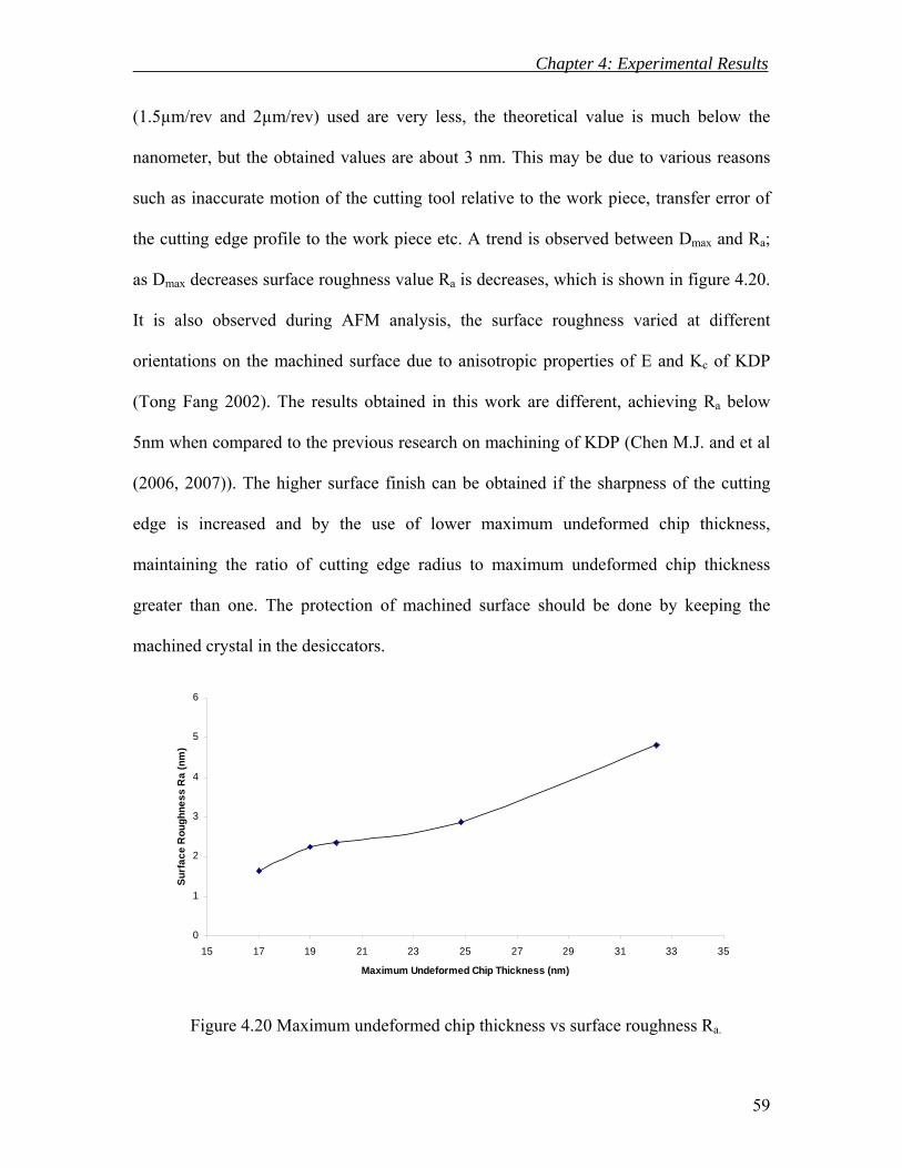
Chapter 4: Experimental Results
59
(1.5µm/rev and 2µm/rev) used are very less, the theoretical value is much below the
nanometer, but the obtained values are about 3 nm. This may be due to various reasons
such as inaccurate motion of the cutting tool relative to the work piece, transfer error of
the cutting edge profile to the work piece etc. A trend is observed between Dmax and Ra;
as Dmax decreases surface roughness value Ra is decreases, which is shown in figure 4.20.
It is also observed during AFM analysis, the surface roughness varied at different
orientations on the machined surface due to anisotropic properties of E and Kc of KDP
(Tong Fang 2002). The results obtained in this work are different, achieving Ra below
5nm when compared to the previous research on machining of KDP (Chen M.J. and et al
(2006, 2007)). The higher surface finish can be obtained if the sharpness of the cutting
edge is increased and by the use of lower maximum undeformed chip thickness,
maintaining the ratio of cutting edge radius to maximum undeformed chip thickness
greater than one. The protection of machined surface should be done by keeping the
machined crystal in the desiccators.
0
1
2
3
4
5
6
15 17 19 21 23 25 27 29 31 33 35
Maximum Undeformed Chip Thickness (nm)
Surf
ace
Rou
ghne
ss R
a (n
m)
Figure 4.20 Maximum undeformed chip thickness vs surface roughness Ra.

60
CHAPTER 5
CONCLUSIONS
The following important conclusions drawn from the experimental investigation
are shown below
1. Experimental results show that ductile surfaces could be achieved on the soft
and brittle material like KDP with the surface roughness below 5nm from AFM analysis
which is required in the KDP applications.
2. Dry cutting of KDP is proposed in this work considering the disadvantages
when suitable coolant is used such as occurrence of ‘Fogging’.
3. The main challenge identified in dry cutting of KDP is removal of machined
chips. These machined chips cause surface damage which leads to poor surface integrity.
4. To overcome this problem, a Venturi Vacuum Suction Technique is proposed
to extract the chips from the machined zone.
5. The applicability of Venturi Vacuum Suction Technique is shown theoretically
based upon the conditions that the chip flow velocity into the suction port should be
greater than the chip velocity and suction flow rate (SCFM) should be more than material
removal rate.
• Chip Velocity is calculated from Merchant’s theory of cutting and a factor is
considered for estimation of chip flow velocity.
• Suction flow rate (SCFM) and suction pressure required are calculated from
the size of the venturi nozzle.

Chapter 5: Conclusions
61
6. The implementation of vacuum suction for extraction of chips is performed
maintaining the conditions mentioned previously and results showed that it is possible to
eliminate chips from the work zone and machined surface, leaving a fracture free optical
surface on the KDP material.
It is concluded that KDP, as proposed in this work, should be diamond turned in
dry cutting conditions to avoid the sub-surface damage caused due to cleaning process
that involved when machining oil is used (mentioned in literature); which aggravates the
damage due to the intrinsic behavior of the KDP material. The difficulties encountered
during dry machining of KDP are resolved by proposing the extraction of chips by
vacuum and experiment results showed obtaining the chip free, fracture free optical
surface with surface roughness that can be directly used in the applications.

62
CHAPTER 6
REFERENCES
Baruch A. Fuchs, P. Paul Hed, and Phillip C. Baker, ‘Fine Diamond Turning of KDP
Crystals’, Applied Optics, Vol. 25, No. 11, 1986.
Baruch A. Fuchs et al, ‘Diamond turning of L-arginine phosphate, a new organic
nonlinear crystal’, Applied Optics, 28, 20, 1989, p 4465-4472.
Baruch A. Fuchs, C. Syn and S.P. Velsko, ‘Diamond Turning of Lithium Niobate for
Optical Applications’, Applied Optics, Vol. 31, No. 27, 1992.
Beltrao P.A, A.E. Gee, J. Corbett and R.W. Whatmore, ‘Ductile Mode Machining of
Commercial PZT Ceramics’, Annals of the CIRP, 48, 1999, p 437-440.
Blake N Peter, ‘Ductile Regime Machining of Germanium and Silicon’, Journal of
American Ceramic Society, 73, 4, 1990, p 949-957.
Blackley W.S. and Scattergood R.O, ‘Ductile Regime machining model for diamond
turning of brittle materials’, Precision Engineering, 1991, p 95-103.
Bifano T.G, T.A. Dow and R.O. Scattergood, ‘Ductile Regime Grinding: A New
Technology for Machining Brittle Materials, Transactions of the ASME, 113, 1991, p
184-189.
Bridgeman P.W, ‘Effects of Very High-Pressure on Glass’, Journal of Applied Physics,
24, 1953, p 405-413.
Brinksmeier E, O. Riemer, ‘Measurement of Optical Surfaces Generated by Diamond
Turning’, International Journal of Machine tools manuf., vol. 38, 5-6, 1998, p 699-
705.

Chapter 6: References
63
Chen M. J et al, ‘Research on Influence of Crystal KDP Anisotropy on Critical Condition
of BDT in Ultra precision Cutting’, Key Engineering Materials, Vols. 315-316, 2006,
p 725-730.
Chen M. J, J. H. Wang, X. M. Chen , Y. C. Liang, ‘Analysis of Mechanical Property of
Crystal KDP and Simulation of Ultra-precision cutting process in the ductile mode’,
Key Engineering Materials, Vol. 329, 2007, p 427-432.
Fang F. Z and Venkatesh V. C, ‘Diamond Cutting of Silicon with Nanometric Finish’,
Annals of the CIRP, Vol. 47/1/1998, p 45-49.
Fang F. Z. and Zhang G. X, ‘An experimental study of edge radius effect on cutting
single crystal silicon’, International Journal of Advanced Manufacturing Technology,
22, 2003, p 703-707.
Geoffrey Boothroyd and Winston A Knight, ‘Fundamentals of machining and machine
tools’.
Glass A. J. and Guenther A. J, ‘Damage in Laser Materials’, Applied Optics 11, 1972, p
832-840.
Hou Jing, Zhang Jianfeng, Chen Jinlin, Zhang Xiali, Hu Dezhi, ‘Surface quality of large
KDP crystal fabricated by single point diamond turning’, Proceedings of SPIE, Vol.
6149, 2006.
Huerta M and Malkin S, ‘Grinding of Glass: The Mechanics of the Process’, ASME
Transactions, Journal of Engineering for Industry, 98, 1976, p 459-467.
Ikawa Naoya et al, ‘Ultraprecision Metal Cutting – The Past, the Present and the Future’,
Annals of the CIRP, 40, 2, 1991, p 587-594.

Chapter 6: References
64
Jiwang Yan et al, ‘Single Point Diamond Turning of CaF2 for nanometric surfaces’,
International Journal of Advanced Manufacturing Technology, 24, 2004, p 640-646.
John Patten et al, ‘Ductile Regime Nanomachining of Single Crystal Silicon Carbide’,
Transactions of the ASME, 127, 2005, p 522-532.
Johnson K. L, ‘The core-relation of Indentation Experiments’, Journal of the Mechanics
and Physics of Solids, 18, 1970, p 115-126.
Komanduri R, ‘Some Aspects of Machining with Negative Rake Tools Simulating
Grinding’, Int. J. Mach. Tool Des Res., 11, 1971, p 223-233.
Komanduri R, N. Chandrasekaran, L. M. Raff, ‘Effect of Tool Geometry in Nanometric
Cutting: A molecular Dynamic Simulation Approach’, Wear, 219, 1998, p 84-97.
Kozlwski M. R et al, ‘Influence of Diamond Turning and Surface Cleaning Processes on
the Degradation of KDP Crystal Surfaces’, SPIE Vol. 1561, Inorganic Crystals for
Optics, Electro-optics and Frequency Conversion, 1991, p 59-69.
King R. F. and D. Tabor, ‘The Strength Properties and Frictional Behavior of Brittle
Solids’, Proceedings of the Royal Society of London, Series A: Mathematical and
Physical Science, 223, 1954, p 225-238.
Kucheyev S. O et al, ‘Mechanical response of DKDP crystals during nanoindentation’,
Applied Physics Letters, Vol. 84, 13, 2004, p 2274-2276.
Lawn B. R and A. G. Evans, ‘A Model for Crack Initiation in Elastic/Plastic Indentation
Fields’, Journal of Materials Science, 12, 1977, p2195-2199.
Lawn B. R, A. G. Evans, D. B. Marshall, ‘Elastic-Plastic Indentatin Damage in Ceramics:
The Median Radial Crack System’, Journal of American Ceramic Society, 63, 1980, p
574-581.

Chapter 6: References
65
Lawn B. R et al, ‘Making Ceramics Ductile’, Science, 263, 1994, p 1114-1116.
Leung T. P, W. B. Lee, X. M. Lu, ‘Diamond Turning of Silicon Substrates in Ductile
Regime’, Journal of Materials Processing Technology, 73, 1998, p 42-48.
Liu Kui, ‘Ductile Cutting for Rapid Prototyping of Tungsten Carbide Tools’, PhD Thesis,
2002.
Li X. P, M. Rahman, K. Liu, K. S. Neo, C. C. Chan, ‘Nano-precision measurement of
diamond tool edge radius for wafer fabrication’, Journal of Materials Processing
Technology, 140, 2003, p 358-362.
Lucca D. A et al, ‘Effect of Tool Edge Geometry on the Nanometric Cutting of Ge’,
Annals of the CIRP, Vol. 47/1, 1998, p 475-478.
Marsh R Eric et al, ‘Predicting surface figure in diamond turned calcium fluoride using in
process force measurement’, Journal of Vacuum Science and Technology, B 23, 1,
2005, p 84-89.
Marvin J Weber, ‘Handbook of Laser Science and Technology’ Volume 5, Optical
Materials, Part 3, 1995.
Moriwaki T. E, Shamoto and K. Inoue, ‘Ultraprecision Ductile Cutting of Glass by
Applying Ultrasonic Vibration’, Annals of the CIRP, 41, 1992, p 141-144.
Morris J.C et al, ‘Origins of the Ductile Regime in SPDT of Semiconductors’, Journal of
the American Ceramic Society, 78, 1995, p 2015-2020.
Nakasuji et al, ‘Diamond Turning of Brittle Materials for Optical Components’, Annals
of the CIRP, vol. 39, 1, 1990, p 89-92.
Nakayama K et al., ‘Cutting Tools with Curved Rake Face-A Means for Breaking Thin
Chips’, Annals of CIRP, 30(1), 1981, p 5-8.
Chapter 6: References
66
Nakayama K, ‘Topics on fundamentals of Precision Machining’, Machining Science and
Technology, 1(2), 1997, p 251-262.
Namba Y and Katagiri M, ‘Ultraprecision grinding of KDP for getting optical surfaces’,
SPIE Vol.3578, 1998.
Namba Y and Saeki M, ‘Optical Surface Generation of Organic Nonlinear Crystals by
Single Point Diamond Turning’, Annals of the CIRP, Vol. 52, 1, 2003, p 475-478.
Ngoi B. K. A. and Sreejith P. S, ‘Ductile Regime Finish Machining – A Review’,
International Journal of Advanced Manufacturing Technology, 16, 2000, p 547-550.
Peter F. Bordui and Martin M. Fejer, ‘Inorganic Crsystals for Nonlinear Optical
Frequency Conversion’, Annual Review of Material Sciences, 1993, p 321-79.
Puttick K. E et al, ‘Single Point Diamond machining of Glasses’, Proc. R. Soc. Lond,
A426, 19/30, 1989.
Puttick K. E et al, ‘Energy Scaling Transitions in Machining of Silicon by Diamond’,
Tribology International, 28, 6, 1995, p 349-355.
Qiao Xu, Jian Wang, Wei Li, Xun Zeng, Shouyong Jing, ‘Defects of KDP Crystal
Fabricated by Single Point Diamond Turning’, SPIE, Vol. 3862, 1999.
Richard C Montesanti, Samuel L Thompson, ‘A Procedure for Diamond Turning KDP
Crystals’, LLNL Report, 1995.
Said Jahanmir, M.Ramulu, Philip Koshy, ‘Machining of ceramics and composites’ 1999.
Sanjib Chatterjee, ‘Simple Technique for Polishing Optical Components made from KDP
group of Crystals’, Journal of Optics, 2005, Vol. 34, No.2, p93-101.
Shaw M. C, ‘A New Theory of Grinding’, Mech Chem Trans Inst Eng Aust, 1, 1972, p
73-78.

Chapter 6: References
67
Shibata T., S. Fujii, E. Makino and M. Ideda, ‘Ductile Regime Turning Mechanism of
Single Crystal Silicon’, Precision Engineering, 18, pp.325-328, 1996.
Shimada Shoichi et al, ‘Brittle-Ductile Transition Phenomena in Microindentation and
Micromachining’, Annals of the CIRP, 44, 1, 1995.
Syn Chol K et al, ‘Diamond Turning: Optimum Machining of Optical Crsytals’,
Mechanical Engineering, 1991, 113, 4, p 68-72.
Tong Fang, ‘Microhardness and Indentation Fracture of KDP’, Journal of American
Ceramic Society, 85, 1, 2002, p 174-178.
Wood R M. et al, ‘Laser damage in Optical materials at 1.06µm’, Optics and Laser
Technology, Vol. 6, 1975, 105-111.
Yoshiharu Namba et al, ‘Single Point Diamond Turning of KDP Inorganic Nonlinear
Optical Crystals for Laser Fusion’, Journal of Japan Society, Vol. 64, no. 10, 1998, p
1487-1491 (Japanese).
Yoshido H et al, 2000 crystal structure.
http://www.teknocraft.com
http://www.clevelandcrystals.com/KDP.htm