nanopla overview yao guo oct 6, 2005. semiconducting nanowires few nm’s in diameter (e.g. 3nm)...
Post on 21-Dec-2015
216 views
TRANSCRIPT

NanoPLA Overview
Yao Guo
Oct 6, 2005

Semiconducting Nanowires
• Few nm’s in diameter (e.g. 3nm)– Diameter controlled by seed catalyst
• Can be microns long
• Control electrical properties via doping– Materials in environment during growth– Control thresholds for conduction
From: Cui…Lieber APL v78n15p2214

SiNWGrowth
• Atomic structure determines feature size
• Self-same crystal structure constrains growth
• Catalyst defines/constrains structure

SiNW Growth

SiNW Growth

Homogeneous Crossbar
• Gives us homogeneous NW crossbar– Undifferentiated wires– All do the same thing

Control NW Dopant
• Can define a dopant profile along the length of a wire– Control lengths by timed growth– Change impurities present in the envir
onment as a function of time
Gudiksen et. al. Nature 415 p617
Björk et. al. Nanoletters 2 p87

Control NW Dopant
• Can define a dopant profile along the length of a wire– Control lengths by timed growth– Change impurities present in the envir
onment as a function of time
• Get a SiNW banded with differentiated conduction/gate-able regions
Gudskien et. al. Nature 415 p617
Björk et. al. Nanoletters 2 p87

Enables: Differentiated Wires
• Can engineer wires– Portions of wire always
conduct) – Portions controllable

Coded Wires
• By selectively making bit-regions on wires either highly or lightly doped– Can give the wire an address

Unique Set of Codes
• If we can assemble a set of wires with unique codes– We have an address
decoder

Unique Set of Codes
• If we can assemble a set of wires with unique codes– We have an address
decoder• Apply a code
– k-hot code
• Unique code selects a single wire

Devices
Diode and FET Junctions
Doped nanowires give:
Huang…LieberScience 294 p1313
Cui…LieberScience 291 p851
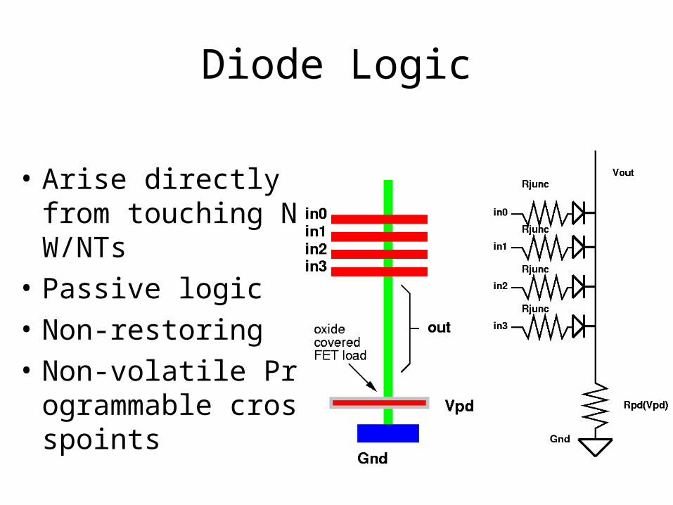
Diode Logic
• Arise directly from touching NW/NTs
• Passive logic
• Non-restoring
• Non-volatile Programmable crosspoints
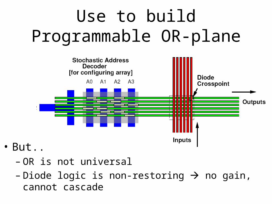
Use to build Programmable OR-plane
• But..– OR is not universal– Diode logic is non-restoring no gain, cannot
cascade
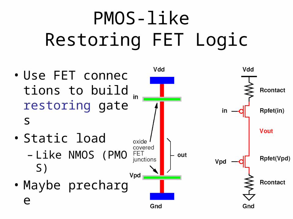
PMOS-like Restoring FET Logic
• Use FET connections to build restoring gates
• Static load– Like NMOS (PMO
S)
• Maybe precharge

Ideal vs. Stochastic Restore

Simple Nanowire-Based PLA
NOR-NOR = AND-OR PLA Logic

Defect Tolerant
All components (PLA, routing, memory) interchangeable;Have M-choose-N propertyAllows local programming around faults

Crosspoint Defects• Crosspoint junctions may be
nonprogrammable– E.g. HPs first 8x8 had 85% pr
ogrammable crosspoints
• Tolerate by matching nanowire junction programmability with pterm needs
• Less than ~10% overhead for crosspoint defect rates up to 20%
Naeimi/DeHon, FPT2004

Interconnected nanoPLAs

Tile into Arrays

Manhattan Routing

Manhattan Routing

Tile into Arrays

Complete Substrate for Computing
• Know NOR gates are universal
• Selective inversion• Interconnect structure for arb
itrary routingCan compute any logic functi
on
• Can combine with nanomemories

Interconnected nanoPLA Tile

Area Mapped Logic
• Take standard CAD/Benchmark designs– Toronto20 used for FPGA evaluation
• Map to PLAs
• Place and Route on arrays of various configurations
• Pick Best mapping to minimize Area
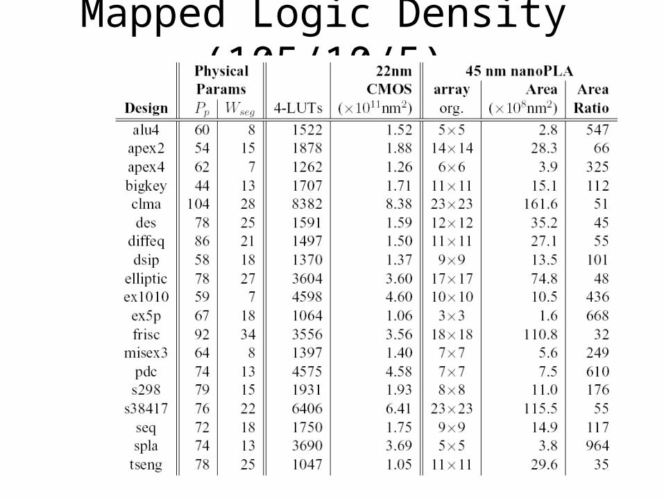
Mapped Logic Density (105/10/5)

Cycle Delay:105/10/5/Ideal Restore/Pc=0.95

Power Density (per GHz)
• Vdd=1V• Active Power• Precharge

Comparison to NASIC
• Area Efficiency:– NanoPLA wastes most of the area in routing.– NASIC should be more efficient in area usage.
• Density Comparison:– NanoPLA: up to 1000X denser than 22-nm CMOS PLA– NASIC: up to 100X denser than 30-nm ASIC
• Fault Tolerance– Fault tolerance is easier in NanoPLA because you can pr
ogram around defects.

Memories

Basis for Sublithographic Memory

Precharge all lines low

Drive Column Read Address

Pulls Single Column Line High

On xpoint allow to pull Row lines to be pulled high
Assume here: only the two points shown are “on”.i.e. column has 0 1 0 0 1 0

All Rows Disabled
Read outputnot driven;sees 0

Select Read Row 1010
Read outputnow pulledhigh; sees 1

Select Read Row 1100
Read outputnot driven;sees 0