nanoelectronics: current generation, new formulation of
TRANSCRIPT

JOURNAL OF NANO- AND ELECTRONIC PHYSICS ЖУРНАЛ НАНО- ТА ЕЛЕКТРОННОЇ ФІЗИКИ
Vol. 5 No 1, 01023(15pp) (2013) Том 5 № 1, 01023(15cc) (2013)
2077-6772/2013/5(1)01023(15) 01023-1 2013 Sumy State University
Nanoelectronics: Current Generation, New Formulation of Ohm's Law and
Conduction Modes by "Bottom-Up" Approach
Yu.A. Kruglyak1, P.A. Kondratenko2, Yu.M. Lopatkin3
1 Odessa State Environmental University, 15, Lvivska str., 65016 Odessa, Ukraine 2 National Aviation University, 1, Komarov ave., 03058 Kyiv, Ukraine
3 Sumy State University, 2, Rymsky-Korsakov str., 40007 Sumy, Ukraine
(Received 18 January 2013; revised manuscript received 13 February 2013; published online 28 March 2013)
General questions of electronic conductivity, current generation with the use of electrochemical poten-
tials and Fermi functions, elastic resistor model, ballistic and diffusion transport, conductivity modes, n-
and p-conductors and graphene, new formulation of the Ohm’s law are discussed in the frame of the «bot-
tom-up» approach of modern nanoelectronics.
Keywords: Nanoelectronics, Moletronics, Bottom-Up, Ohm’s law.
PACS numbers: 71.15.Mb, 71.20. – b, 73.22.Pr, 73.23.Ad, 84.32.Ff, 85.35. – p
1. INTRODUCTION
The rapid development of nanoelectronics in the
last 10-15 years has led not only to the creation and
wide use of nanotransistors and a variety of nanoscale
electronic devices, but also to the deeper understanding
of the causes of current, exchange and energy dissipa-
tion, and the operation principles of nanoscale devices
as well as conventional electronic devices [1-4]. Nowa-
days, the revolutionary changes in electronics require
reviewing the content of physics studies at the univer-
sity. A similar revolutionary situation was 50 years ago
after the discovery of the transistor, which led not only
to the widespread use of microelectronic devices, but
also to a radical revision of the university and engi-
neering courses of General Physics, not to mention the
special courses in electronics and related disciplines.
The materials and substances used in electronics are
characterized by such integral properties as carrier
mobility and optical absorption coefficient, with further
use to explain the observed physical phenomena and
modeling of various electronic devices from the time of
formation physics of solid state. Now with the shift to
meso- and nanoscopic the nano- and molecular transis-
tors require using of laws of quantum mechanics and
non-equilibrium statistical thermodynamics for its de-
scription and simulation from the very outset, which
inevitably leads to a revision of university physics
courses at the beginning.
According to Ohm's law, the resistance R and con-
ductance G of the conductor with length L and cross-
sectional area A are given by expressions:
/ / and 1/ /R V I L A R G A L , (1)
where the resistivity ρ and its inverse conductivity
does not depend on the geometry of the conductor and
the properties of the material from which the conductor
is made. Ohm's law says that length reduction of the
conductor several times reduces the resistance in the
same number of times. And if we reduce the length of
the conduction channel to a very small size, does it
mean that the resistance will be almost "neutral earth-
ing"?
With usual "diffusive" motion of electrons through a
conductor the mean free path in conductor is less than
1 micron and varies widely, depending on the tempera-
ture and the nature of the conductor material. The
length of the conduction channel in the current FET is
~ 40 nm, which are few hundred atoms. It is appropri-
ate to ask the question: if the length of the conductor is
less than the diffusion length of the mean free path,
does the electron motion become ballistic? Will re-
sistance obey Ohm's law in the usual record? And what
if one reduces the length of the conduction channel to a
few atoms? Does it make sense to speak of the re-
sistance in itself? All these questions were the hot dis-
cussion topic 15-20 years ago. Nowadays the answers to
these questions are given and reliably supported by
numerous experimental data. And even the resistance
of the hydrogen molecule was measured. [5]
Attention is drawn to the fact that the impressive
success of the experimental nano-electronics didn’t
have any effect on the way we think, learn, and explain
the concept of resistance, conductivity and operation of
electronic devices in general. And until now, apparent-
ly, for historical reasons the familiar concept of "top-
down" from the massive conductors to molecules domi-
nates. This approach was acceptable as long as there
was not enough experimental data on the measure-
ment of conductivity of nanoscale conductors. In the
last decade, the situation has changed. Vast experi-
mental data are accumulated for large and maximum
small conductors. The development of the concept of
"bottom-up" conductivity, which was not only found to
be complementary to concept of "top-down" but also led
to a rethinking of the operation principles of conven-
tional electronic devices, has begun [6-8]. Recall that
the concept of "bottom-up" from the hydrogen atom in
the direction of the solid dominates in quantum me-
chanics from the start.
There is another range of problems in nanoelectro-
nics, for which the concept of "bottom-up" is very inter-
esting. This is the transport problem. In conventional
electronics transport of particles is described by the
laws of mechanics-classical or quantum. Transport in
bulk conductors is accompanied by heat, which is de-

YU.A. KRUGLYAK, P.A. KONDRATENKO, YU.M. LOPATKIN J. NANO- ELECTRON. PHYS. 5, 01023 (2013)
01023-2
scribed by the laws of thermodynamics-conventional or
statistical. Processes are reversible in mechanics, and
irreversible in thermodynamics. Strictly speaking, it is
impossible to separate these two processes – the
movement and heat. There is quite different situation
in nanoelectronics. Here the process of electron motion
and heat are spatially separated: the electrons move
elastically, ballistic ("elastic resistance"), and heat gen-
eration occurs only at the interface of the conductor
and the electrodes. The concept of "elastic resistor" was
proposed by Landauer in 1957 [9-11] long before its
experimental confirmation in nanotransistors. The con-
cept of "elastic resistor", properly speaking, is an ideal-
ization, but it is reliably confirmed by numerous exper-
imental data for the ultra-small nanotransistors. The
development of the concept of "bottom-up" [12] has led
to the creation of the unified picture of transport phe-
nomena in nanoscale electronic devices as well as in
macrodimension ones.
The paper presents the causes of the origin of cur-
rent and the role of electro-chemical potentials under
the concept of "bottom-up" and the Fermi functions in
this process. Furthermore, the model of «elastic resis-
tor» is considered and a new formulation of Ohm's law
is given. Within the framework of conception "below-
up" the general questions of electronic conductivity will
also be considered, including the example of graphene.
2. THE CAUSE OF THE CURRENT
When asked about the cause of current by applying
the potential difference at the ends of the conductor
usually refer to the relationship of the current density j
and the external applied electric field E
j E, (2)
in other words, electric field is usually considered the
cause of current. The answer is, at the best case, in-
complete. Before connecting conductor to the cleats of
the voltage source the strong electric fields created by
nuclei affects electrons of the conductor and current is
still not arise. Why do the strong internal electric fields
not cause the movement of electrons, but much weaker
external electric field of battery causes movement of
electrons? It is usually said that the internal micro-
scopic fields can’t cause movement of the electrons, it is
necessary to attach an external macroscopic field. This
explanation can not be satisfactory. It is impossible
definitively separate the internal and external electric
fields in present-day experiments of measuring the
individual molecules conductivity. We have to take this
lesson learned us by present experimental nanoelec-
tronics, and re-ask the question why the electrons move
when the battery is connected to the ends of the con-
ductor.
To answer the question about the cause of current
from the start we need two concepts – the density of
free states, those occupied by electrons per unit energy
D (E) and electrochemical potential 0 (Fig. 1). For
simplicity's sake, that will not affect the final conclu-
sions, we will use the point model of conductor (the
channel of electron transfer), which assumes the im-
mutability of the density of states D (E) as they move
along a conductor. If the system comprising the source
electrode (S / Source), conductor M and stock electrode
(D / Drain) are in equilibrium (shorted), the electro-
chemical potential 0 is the same everywhere, and all
states with E < 0 filled with electrons, and the states
with E > 0 are empty (Fig. 1).
Fig. 1 – The first step in explaining the operation of any elec-
tronic device should be setting the density of states D (E) as
the function of the energy E in the conductor M and determi-
nation of the equilibrium value of the electrochemical poten-
tial 0, separating the occupied electron states from empty
states
When the voltage source in the circuit (Fig. 2) the
potential difference V reduces all energies on the posi-
tive electrode D on the value of qV, where q – charge of
electron, resulting in the electrodes the electrochemical
potential difference is created
1 2– qV . (3)
Just as the temperature difference causes heat flow,
and the difference in the levels of fluid leads to its
flows, and electrochemical potential difference is the
cause of the current. Only the state of the conductor in
the interval 1 – 2 and located enough close to the val-
ues of 1 and 2 contribute to the electron flow, while
all the state that are much higher μ1 and lower 2 do
not play any role. The reason is as follows.
Each contact seeks to lead the current channel to
the equilibrium with itself by filling all the states of the
channel with electrons with energy less than the elec-
trochemical potential 1, and emptying of states of
channel with energy greater than the potential μ2.
Consider the current channel with the states with en-
ergy less than 1, but more 2. Contact 1 is seeking to
fill these states, because their energy is lower than 1,
and contact 2 tends to empty these states because their
energy is greater than 2, which leads to the continu-
ous movement of electrons from contact 1 to contact 2.
Now consider the state of the channel with energy
greater than 1 and 2. Both contacts tend to empty
these states, but they are empty and do not make their
contribution to the electrical current. The situation is
similar to the states when energy is less at the same
time than both potentials μ1 and μ2. Each contact is
seeking to fill them with electrons, but they are already
filled, and can’t make the contribution to the current,
NANOELECTRONICS: CURRENT GENERATION, NEW FORMULATION… J. NANO- ELECTRON. PHYS. 5, 01023 (2013)
01023-3
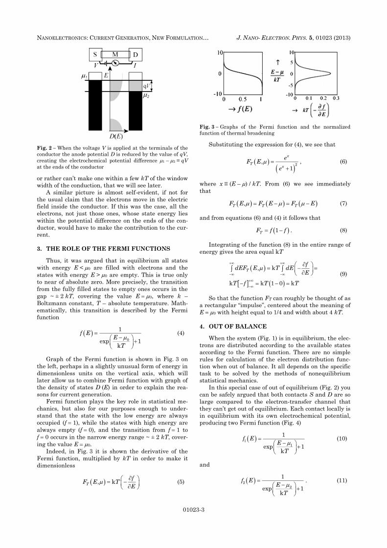
Fig. 2 – When the voltage V is applied at the terminals of the
conductor the anode potential D is reduced by the value of qV,
creating the electrochemical potential difference 1 – 2 = qV
at the ends of the conductor
or rather can’t make one within a few kT of the window
width of the conduction, that we will see later.
A similar picture is almost self-evident, if not for
the usual claim that the electrons move in the electric
field inside the conductor. If this was the case, all the
electrons, not just those ones, whose state energy lies
within the potential difference on the ends of the con-
ductor, would have to make the contribution to the cur-
rent.
3. THE ROLE OF THE FERMI FUNCTIONS
Thus, it was argued that in equilibrium all states
with energy E < 0 are filled with electrons and the
states with energy E > 0 are empty. This is true only
to near of absolute zero. More precisely, the transition
from the fully filled states to empty ones occurs in the
gap ~ ± 2 kT, covering the value E 0, where k –
Boltzmann constant, T – absolute temperature. Math-
ematically, this transition is described by the Fermi
function
0
1
exp 1k
f EE
T
(4)
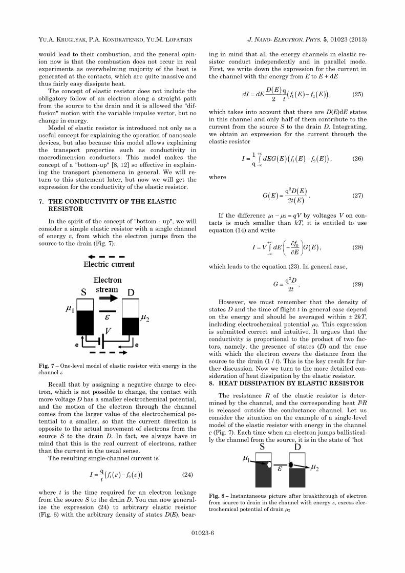
Graph of the Fermi function is shown in Fig. 3 on
the left, perhaps in a slightly unusual form of energy in
dimensionless units on the vertical axis, which will
later allow us to combine Fermi function with graph of
the density of states D (E) in order to explain the rea-
sons for current generation.
Fermi function plays the key role in statistical me-
chanics, but also for our purposes enough to under-
stand that the state with the low energy are always
occupied (f 1), while the states with high energy are
always empty (f 0), and the transition from f 1 to
f 0 occurs in the narrow energy range ~ ± 2 kT, cover-
ing the value E 0.
Indeed, in Fig. 3 it is shown the derivative of the
Fermi function, multiplied by kT in order to make it
dimensionless
, kT
fF E T
E
(5)
Fig. 3 – Graphs of the Fermi function and the normalized
function of thermal broadening
Substituting the expression for (4), we see that
2,
1
x
Tx
eF E
e
, (6)
where x ≡ (E – ) / kT. From (6) we see immediately
that
,T T TF E F E F E (7)
and from equations (6) and (4) it follows that
1TF f f . (8)
Integrating of the function (8) in the entire range of
energy gives the area equal kT
, k
k k 1 0 k
T
fdEF E T dE
E
T f T T
(9)
So that the function FT can roughly be thought of as
a rectangular “impulse”, centered about the meaning of
E 0 with height equal to 1/4 and width about 4 kT.
4. OUT OF BALANCE
When the system (Fig. 1) is in equilibrium, the elec-
trons are distributed according to the available states
according to the Fermi function. There are no simple
rules for calculation of the electron distribution func-
tion when out of balance. It all depends on the specific
task to be solved by the methods of nonequilibrium
statistical mechanics.
In this special case of out of equilibrium (Fig. 2) you
can be safely argued that both contacts S and D are so
large compared to the electron-transfer channel that
they can’t get out of equilibrium. Each contact locally is
in equilibrium with its own electrochemical potential,
producing two Fermi function (Fig. 4)
11
1
exp 1k
f EE
T
(10)
and
22
1
exp 1k
f EE
T
. (11)

YU.A. KRUGLYAK, P.A. KONDRATENKO, YU.M. LOPATKIN J. NANO- ELECTRON. PHYS. 5, 01023 (2013)
01023-4
Fig. 4 – When they get out of balance the electrons in the
contacts take available to them the states in accordance with
the Fermi distribution, and the values of electrochemical po-
tentials
Summing up, it is stated that the reason of the cur-
rent is the difference in the preparation of the equilibri-
um states of contacts, displayed by their respective Fer-
mi function f1(E) and f2(E). Qualitatively, this is true for
any conductors – nanoscale and macrodimension ones.
However, for nanoscale conductors the current is propor-
tional to the difference I (E) ~ f1 (E) – f2 (E) of the Fermi
distributions in both contacts at any value of the energy
of the electronic states in a conductor. This difference
vanishes if the energy E is greater 1 and 2, as in this
case; both the Fermi functions are zero. This difference
also vanishes if the energy E is smaller 1 and 2, as in
this case, both the Fermi functions are equal to one.
Current arises only in the window 1 – 2, if it contains
at least one electronic state of the conductor.
5. LINEAR RESPONSE
The current-voltage characteristic is usually non-
linear, but it could be single out plot of "linear re-
sponse", which implies conductance dI / dV at V → 0.
We construct the function of the difference of the
two Fermi functions, normalized to the applied voltage
1 2
q / k
f E f EF E
V T
, (12)
Where
1 0
2 0
q / 2
q / 2
V
V
. (13)
Function of the difference F (E) is narrowed as the
voltage V, multiplied by the charge of the electron, be-
comes smaller than kT (Fig. 5). Note also that as kT
begins to exceed the energy qV, function F (E) is get-
ting closer to the function of the thermal broadening (5)
F (E) → FT (E) at qV / kT → 0, so that from equations
(12) follows that
01 2 0
q, q
kT
fVf E f E F E V
T E
(14)
if the applied voltage multiplied by the electron charge,
1 – 2 qV becomes much smaller kT.
We also need the following expression
00 0
ff E f E
E
(15)
Fig. 5 – The graph of the difference F (E) depending on the
value (E – 0) / kT for different qV / kT ≡ y
which, like the equation (14), can be obtained as fol-
lows.
For the Fermi function
1
,k1x
Ef x x
Te
(16)
we have
2
1
k
1
k
k
f df x df
E dx E dx T
f df x df
dx dx T
f df x df E
T dx T dx T
, (17)
where from
f f
E
f E f
T T E
. (18)
Equation (15) is obtained from the decomposition of
the Fermi function in Taylor series near the point of
equilibrium
0
0 0, ,f
f E f E
. (19)
From equation (18) it follows
00
f f
E
. (20)
Let f(E) corresponds to f(E, ), and f0(E) corresponds
to f (E, 0), then
0 0
ff E f E
E
, (21)
that after rearrangement gives the required equation
(15), which is true for – 0 << kT.

NANOELECTRONICS: CURRENT GENERATION, NEW FORMULATION… J. NANO- ELECTRON. PHYS. 5, 01023 (2013)
01023-5
Preliminary results. Conductivity of materials can
vary by more than 1020 times, going, for example, from
silver to glass – the substances that very distant from
each other in the scale of conductivity. The standard
explanation for the difference in the conductivity is
alleged that the density of "free electrons" in these ma-
terials is very different. This explanation immediately
requires explanations which electrons are free, and
which are not. This difference becomes more and more
absurd as the transition to the nanoscale conductors.
The concept of "bottom-up" offers the following sim-
ple answer. Conductivity depends on the density of
states in the window with width of a few kT, covering
the equilibrium electrochemical potential μ0, defined by
the function FT (equation 5, Fig. 3), which is different
from zero in a small gap with width a few kT around
the equilibrium value of the electrochemical potential.
It's not in the total number of electrons, which is of
the same order as in silver, and in the glass. The key
point is the presence of the electronic states in the
range of meaning of electrochemical potential 0 that
basically distinguishes one substance from another.
The real answer is not new, and it is well known to
experts in the field of nanoelectronics. However nowa-
days discussion usually starts with the Drude theory
[13], which has played an important historical role in
understanding the nature of the current. Unfortunate-
ly, the approach of the Drude spawned two misunder-
standings that should be overcome, and especially in
the teaching of physics, such as:
(1) Current is generated by an electric field;
(2) Current depends on the number of electrons.
Both misconceptions related to each other, as if the
current would indeed be generated by an electric field,
then all the electrons would be affected by the field.
Lessons learned from our experimental nanoelec-
tronics, show that the current generated by the "prepa-
ration" of the two contacts f1(E) – f2(E), and this differ-
ence is not zero only in the window around the equilib-
rium electrochemical potential 0. Conductivity of the
channel is high or low depends on the availability of
the electronic states in the window. This conclusion
usually come through the Boltzmann transport equa-
tion [14] or Kubo formalism [15], while we use the con-
cept of "bottom-up" immediately gives a physically cor-
rect picture of the current.
6. MODEL OF ELASTIC RESISTANCE
Thus, the current generated by the "preparation" of
the two contacts 1 and 2 with the Fermi functions f1(E)
and f2(E). The larger value of the electrochemical po-
tential corresponds to negative terminal 1, and a lower
value – to positive. Negative terminal is willing to
transfer the electrons in the conduction channel, and
positive contact seeks to extract electrons from the
conduction channel. This is true for any conductors –
either nanoscale, or macrodimension.
Model of elastic resistor serves as a useful idealiza-
tion that provides physically correct explanation of
functioning of nanoscale conductors and opens the pos-
sibility for a new interpretation of macrodimension
devices. Rolf Landauer proposed the concept of «elastic
resistor» in 1957 [9-11] long before its experimental
confirmation in nanotransistor. [1] The concept of
"elastic resistor", strictly speaking, is an idealization,
but it is reliably confirmed by numerous experimental
data for ultra small nanotransistors. [3] Development
of the concept of elastic resistor [6-8, 12] has led to the
creation of a unified picture of transport phenomena in
electronic devices of any dimension.
In the elastic resistor model electrons swaps the
conduction channel from the source contact S to stock
one D elastically, without loss or acquisition of energy
(Fig. 6).
Fig. 6 – In the elastic resistor electrons move ballistically
through the channels with constant energy
Current in the range of energy from E to E + dE is
separated from the channel in the elastic resistor with
different values of energy that allows us to write for the
current in the differential form
1 2dI dEG E f E f E , (22)
and after integration to obtain an expression for the
total current. Then, using the expression (14), we ob-
tain the expression for the low voltage conductivity
(linear response)
0fIG dE G E
V E
, (23)
in which the negative derivative (– ðf0 / ðE) can be
thought as a rectangular impulse, whose area is equal
to one and the width ~ ± 2 kT (Fig. 3). According to
(23), the conductivity function G(E) for the elastic resis-
tor, being averaged over the range of ~ ± 2 kT, which
includes the value of the electrochemical potential 0,
gives the experimentally measured conductance G. At
low temperatures, you can simply use the value of G(E)
with E 0.
Such energetic approach to the conductivity in the
elastic resistor model provides the significant simplifi-
cation in understanding of the current causes, although
it sounds paradoxical, because we traditionally associ-
ate the current I through the conductor with the re-
sistance R and the Joule heat I2R. How can we talk
about resistance when electrons moving through a con-
ductor do not lose energy?
The answer is that since the electrons do not lose
energy when driving on elastic resistor, energy loss
occurs at the conductor boundary with the source and
stock contacts, where Joule heat is dissipated. In other
words, the elastic resistance, characterized by the re-
sistance R of the conductance channel, dissipates Joule
heat I2R outside of the conductance channel. This is
indicated by the many different experimental meas-
urements, direct and indirect, on the nanoscale conduc-
tors [3, 4], not to mention the fact that the dissipation
of heat, whether a single molecule or nanoconductor,
YU.A. KRUGLYAK, P.A. KONDRATENKO, YU.M. LOPATKIN J. NANO- ELECTRON. PHYS. 5, 01023 (2013)
01023-6
would lead to their combustion, and the general opin-
ion now is that the combustion does not occur in real
experiments as overwhelming majority of the heat is
generated at the contacts, which are quite massive and
thus fairly easy dissipate heat.
The concept of elastic resistor does not include the
obligatory follow of an electron along a straight path
from the source to the drain and it is allowed the "dif-
fusion" motion with the variable impulse vector, but no
change in energy.
Model of elastic resistor is introduced not only as a
useful concept for explaining the operation of nanoscale
devices, but also because this model allows explaining
the transport properties such as conductivity in
macrodimension conductors. This model makes the
concept of a "bottom-up" [8, 12] so effective in explain-
ing the transport phenomena in general. We will re-
turn to this statement later, but now we will get the
expression for the conductivity of the elastic resistor.
7. THE CONDUCTIVITY OF THE ELASTIC
RESISTOR
In the spirit of the concept of "bottom - up", we will
consider a simple elastic resistor with a single channel
of energy ε, from which the electron jumps from the
source to the drain (Fig. 7).
Fig. 7 – One-level model of elastic resistor with energy in the
channel
Recall that by assigning a negative charge to elec-
tron, which is not possible to change, the contact with
more voltage D has a smaller electrochemical potential,
and the motion of the electron through the channel
comes from the larger value of the electrochemical po-
tential to a smaller, so that the current direction is
opposite to the actual movement of electrons from the
source S to the drain D. In fact, we always have in
mind that this is the real current of electrons, rather
than the current in the usual sense.
The resulting single-channel current is
1 2
qI f f
t (24)
where t is the time required for an electron leakage
from the source S to the drain D. You can now general-
ize the expression (24) to arbitrary elastic resistor
(Fig. 6) with the arbitrary density of states D(E), bear-
ing in mind that all the energy channels in elastic re-
sistor conduct independently and in parallel mode.
First, we write down the expression for the current in
the channel with the energy from E to E + dE
1 2
q
2
D EdI dE f E f E
t , (25)
which takes into account that there are D(E)dE states
in this channel and only half of them contribute to the
current from the source S to the drain D. Integrating,
we obtain an expression for the current through the
elastic resistor
1 2
1
qI dEG E f E f E
, (26)
where
2q
2
D EG E
t E . (27)
If the difference 1 – 2 qV by voltages V on con-
tacts is much smaller than kT, it is entitled to use
equation (14) and write
0fI V dE G EE
, (28)
which leads to the equation (23). In general case,
2q
2
DG
t , (29)
However, we must remember that the density of
states D and the time of flight t in general case depend
on the energy and should be averaged within ± 2kT,
including electrochemical potential 0. This expression
is submitted correct and intuitive. It argues that the
conductivity is proportional to the product of two fac-
tors, namely, the presence of states (D) and the ease
with which the electron covers the distance from the
source to the drain (1 / t). This is the key result for fur-
ther discussion. Now we turn to the more detailed con-
sideration of heat dissipation by the elastic resistor.
8. HEAT DISSIPATION BY ELASTIC RESISTOR
The resistance R of the elastic resistor is deter-
mined by the channel, and the corresponding heat I2R
is released outside the conductance channel. Let us
consider the situation on the example of a single-level
model of the elastic resistor with energy in the channel
ε (Fig. 7). Each time when an electron jumps ballistical-
ly the channel from the source, it is in the state of "hot
Fig. 8 – Instantaneous picture after breakthrough of electron
from source to drain in the channel with energy , excess elec-
trochemical potential of drain 2
NANOELECTRONICS: CURRENT GENERATION, NEW FORMULATION… J. NANO- ELECTRON. PHYS. 5, 01023 (2013)
01023-7
electron" at the drain of energy ε, excess electrochemi-
cal potential of drain 2 (Fig. 8).
In the drain contact the dissipation processes quick-
ly dissipate the excess energy – 2. Similarly, on the
source contact "hole" with energy , less than the elec-
trochemical potential 1 of the source, filled with elec-
trons, and the excess energy 1 – dissipates on source
(Fig. 9).
Fig. 9 – After the ballistic flight of the electron from the
source to the drain through the channel with energy , on
source energy 1 – ε is released , and on the drain the energy
– 2 is released, and contacts are in balance again
The total energy dissipated on the contacts is 1 –
μ2 qV. If N electrons skip from the source to the
drain in the time t, then the power dissipated at the
contacts
q /P V I V N t . (30)
Thus, the heat generated by the passage of current
in elastic resistor dissipates on the contacts, which al-
ready has experimental evidence for nano- and meso-
dimensional conductors [16]. The attractiveness of the
elastic resistor model is that the mechanical and ther-
modynamic processes are spatially separated.
9. MODEL OF ELASTIC RESISTOR AND MAC-
ROCONDUCTORS
It is natural to wonder about the validity and use-
fulness of the elastic resistor model to explain and un-
derstand the physics of the phenomenon of current flow
in normal macroconductors, in which the electron mo-
tion is apparently inelastic. In macroconductors inelas-
tic processes are combined with flexible and randomly
distributed throughout the conductor (Fig. 10). We par-
tition a macroconductor with randomly distributed the
inelastic collisions on sequence of elastic resistors
(Fig. 11) of length L, that much shorter than the real
macroconductor, and with the voltage drop between the
adjacent elastic resistors, which is the small fraction of
the potential difference at the ends of the real conduc-
tor 1 – 2 qV. In the partition the lengths L must be
less than the length of Lin, which is the electron mean
free path to the next inelastic collision. While partition-
ing except the condition L < Lin it should be comply the
requirement that the voltage drop between the adja-
cent elastic resistors ΔV < kT / q.
Fig. 10 – In macroconductors the inelastic processes combined
with elastic ones
Fig. 11 – Hypothetical partition of the real macroconductor on
the series of the elastic resistors
Partitioning the large conductor to the elastic resis-
tors requires some care. As will be shown below, the
standard expression for Ohm's law should be changed
to
/R L A , (31)
where A − the cross-sectional area of the conductor, in
which the additional resistance / A does not depend
on the length of the conductor and can be interpreted
as borderline resistance, which occurs at the boundary
of the channel / contact. In the expression (31) is the
length, which is close to the mean free path, so such
modification of Ohm's law is significant only for ballis-
tic conductors (L ~ ) and is not significant for large
conductors (L >> ). However, conceptually, this addi-
tional resistance will be extremely important if using
the hypothetical structure in Fig. 11 to explain the real
situation in Fig. 10. Structure in Fig. 11 has a lot of
boundary interfaces that do not exist in the real situa-
tion (Fig. 10), so you should get rid of the virtual
boundaries. For example, if a resistance (31) character-
izes each section of length L in Fig. 11, the correct ex-
pression for the conductor in Fig. 10, for example, with
the length 3L will be
3 /R L A , (32)
rather than
3 3 /R L A . (33)
Thus, to obtain the correct expression for the con-
ductivity of the long conductor in the frame of the elas-
tic resistor model you should carefully separate the
boundary resistance from the conductor resistance,
depending on its length.
10. BALLISTIC AND DIFFUSIVE TRANSPORT
As we saw above, the conductivity of the elastic re-
sistor is given by (29) 2q / 2G D t .
We will show that the transit time t through the re-
sistor of length L in diffusion mode with the mean free
path is related to the transit time in the ballistic re-
gime tB by ratio
1B
Lt t
. (34)
Substituting (34) into (29) and taking into account
that

YU.A. KRUGLYAK, P.A. KONDRATENKO, YU.M. LOPATKIN J. NANO- ELECTRON. PHYS. 5, 01023 (2013)
01023-8
2q / 2B BG D t (35)
we will finally obtain for the conductivity in the diffu-
sive mode
BGGL
. (36)
Inverting the conductivity (36), we will obtain for
Ohm's law in a new formulation
R LA
, (37)
where
1 1
BA A G
. (38)
Until now, it was the three-dimensional resistor
with a cross-section A (Fig. 12).
Fig. 12 – Conductors of dimension 3d, 2d and 1d
The various experiments are performed on two-
dimensional conductors with a width W and single-
dimensional cross-section. For such 2d-resistors the
corresponding expressions for Ohm's law, obviously,
have the form
W
R L
(39)
where
1 1
BW W G
. (40)
Finally, for one-dimensional conductors we have
R L , (41)
where
1 1
BG
. (42)
We will write Ohm's law compactly for conductors of
all three dimensions
1 1
1, ,R LW A
, (43)
where
1 1 1
1, ,BGW A
. (44)
The expression in the curly brackets corresponds
1d-, 2d-and 3d-conductors. Note that the resistivity
and conductivity have different dimensions, depending
on the dimensions of the conductor, and the conductivi-
ty and the length is still measured in meters and sie-
mens.
Standard Ohm's law says that the resistance tends
to zero with decreasing length of the conductor to zero.
Nobody expects that the resistance becomes zero, but
common consensus is that the resistance tends to the
certain boundary resistance, which can be made arbi-
trarily small with the improvement of measurement
technology. The experimentally established fact is that
under the most carefully prepared contact the observed
minimal resistance is associated with the channel con-
ductance and is independent of the contact [2]. Modi-
fied Ohm's law reflects this fact: even at approaching
the length conductor to zero the residual resistance
associated with the effective length of is remained. It
is appropriate, however, to ask yourself what sense is
to talk about a non-zero length at zero length of the
conductor. The answer is the fact that for nanoscale
conductors neither resistivity ρ, nor the length has
sense separately, and only their product is essential.
11. BALLISTIC AND DIFFUSIVE TRANSPORT
Consider how the density of states D and the time
of flight t in the expression for the conductivity (29)
correlate with the size of the channel in large conduc-
tors. As for the density of states, it is an additive prop-
erty. At two times large channel has twice the electron
states, so that the density of states for large conductors
should be proportional to the volume of the conductor
A∙L.
As for the time of flight t, it is usually considered
two transport modes:
ballistic one with t ~ L and diffusion one with t ~ L2.
Ballistic conductance is proportional to the cross sec-
tional area of the conductor and, according to (29) does
not depend on the length of the conductor. Such "non-
ohmic" behavior is actually observed in nanoscale con-
ductors [17]. As for conductors with diffusive transport
mode, they show normal "ohmic" behavior of the con-
ductivity G ~ A / L.
The difference of the two transport modes can be
explained as follows. In the ballistic regime the time of
flight from the source to the drain
B
Lt
u , (45)
where
zu (46)
is the average velocity of the electrons along the axis z of
the motion direction of electrons from source to drain.
In the case of the diffusion mode time t quadratical-
ly depends on the length of the conductor
2
2
L Lt
u D , (47)
where the value D is the diffusion coefficient in the
frame of theory of random walks [18]
Current
NANOELECTRONICS: CURRENT GENERATION, NEW FORMULATION… J. NANO- ELECTRON. PHYS. 5, 01023 (2013)
01023-9
2zD (48)
where is the mean free time.
Using (45), we rewrite the (47) in the form
12
B
Lut t
D
, (49)
which together with the equation (34) for the length of
yields
2D
u . (50)
To calculate the constants ū according to the equa-
tion (46) and D according to the equation (48) it is re-
quired to the average electrons velocity in the direction
of their movement (axis z) for all angular variables,
depending on the dimension of the conductor d {1, 2,
3}. Simple calculations yield for
2 21d-conductor andz z , (51)
2 22d-conductor 2 / and / 2z z ,(52)
2 23d-conductor / 2 and / 3z z ,(53)
with the result that
2 1
1, ,2
zu E
, (54)
2 2 1 11, ,
2 3zD E
, (55)
or finally for the mean free path we have
2 4
2, ,2 3
D
u
. (56)
We emphasize that the length λ includes a numeri-
cal factor depending on the dimensions of the conduc-
tor, as compared to its standard value of v . Can
we use this standard value of ? Yes, we can, but then
in the new formulation of Ohm's law (43) L should not
only be replaced by L + , but add to L , multiplied by
the numerical factor that depends on the dimension of
the conductor, or use the definition of the length of in
(56). It’s curious that this factor even for one-
dimensional conductor is not equal to one, and is two.
The value of is the mean free time of the flight to the
next encounter. Since the scattering is assumed to be
isotropic, only half of the acts collision leads the elec-
tron from the source to the drain. With regard for the
inverse scattering the length value for for 1d-
conductor is equal 2v.
Now we will obtain the equation for the ballistic
conductance. From equations (35) and (45) we have
2q 2BG Du L , (57)
and substituting equations (54), we obtain
2q 2 1
1, ,2 2
B
DG
L
. (58)
Finally, substituting (56) and (58) into (44) and tak-
ing (55) we will obtain for the conductivity
2 1 11, ,
Dq D
L W A
. (59)
So, the expressions for the conductivity in the bal-
listic mode (59) and diffusion mode (36) are obtained
based on the general expression for the conductivity
(29) and transit times (45) and (47).
12. CONDUCTIVITY MODES
From equation (58) it is shown that the ballistic
conductance is proportional to the density of states per
unit length of the conductor D / L. Since the density of
states is proportional to the volume, it can be expected
that the ballistic conductance is proportional to the
cross sectional area A of the 3d-conductor or width W of
the 2d-conductor.
Numerous experiments have shown [17] that for
nanoscale conductors the ballistic conductivity does not
vary linearly with their cross-sectional area, and mul-
tiple of the quantum of conductance
2q
BG Mh
. (60)
In other words, the real conductor can be considered
as M independent modes of conduction, giving a total
ballistic conduction. Taking into account (58), we ob-
tain for the number of conduction modes
2 1
1, ,2 2
hDM
L
, (61)
and from equations (44) and (60) the conductivity is
expressed through the number of conduction modes M
and the mean free path
2q 1 1
1, ,Mh W A
. (62)
We will explain in complete detail the concept of
conduction modes hereafter.
13. FUNDAMENTAL RELATIONSHIP
Standard expression for the conductivity is given by
the Drude formula [13] relating the conductivity with
the electron density n, the effective mass m and the
mean free time
21 q n
m
, (63)
or using the concept of mobility
q
m
, (64)

YU.A. KRUGLYAK, P.A. KONDRATENKO, YU.M. LOPATKIN J. NANO- ELECTRON. PHYS. 5, 01023 (2013)
01023-10
we have
qn . (65)
On the other hand, it results in two equivalent ex-
pressions for the conductivity in the concept of a "bot-
tom-up", one of which expresses the conductivity
through the product of the density of states and the
diffusion coefficient D (59), and the other − through the
product of the number of modes M in the channel of
conductance and the average mean free path (62).
As the conductance
0fIG dE G E
V E
,
conductivity of the equations (59) and (62) must be av-
erage over the energy of a few kT, including E 0 us-
ing the function of the thermal broadening
0fdE EE
. (66)
Equation (59) is well known, it is deduced in the
standard textbooks on solid state physics [13], which is
not an equivalent equation (62), the deduce of which
usually requires the use of statistical thermodynamics
of irreversible processes such as the Kubo formalism
[14, 15].
As for the Drude model we would like to emphasize
the following. The applicability of the Drude model is
very limited, while the equation for the conductivity
(59) and (62) have the most general meaning. For
example, these equations are applicable to graphene
[19, 20] with nonparabolic behavior of zones and "mass-
less" electrons – with properties that can’t be described
in the Drude model. One of the lessons learned by
nanoelectronics is broad applicability of the equations
for the conductivity (59) and (62).
The fundamental difference between (59) and (62)
and the Drude theory is that the averaging (66) makes
the conductivity as property of the Fermi surface: the
conductivity is determined by the energy levels close to
E 0. And according to the equations (63)-(65) of the
Drude theory conductivity depends on the total electron
density, summed over the entire spectrum of energy,
which leads to the limited applicability of the Drude
model. Conductivity of materials varies widely in spite
of the fact that the number of electrons approximately
equal. Low glass conductivity not because there are few
of so-called "free" electrons in it; glass is characterized
by a very low density of states and the number of
modes near E 0. The concept of a "free" electron be-
longs to intuitive concept.
For any conductor, either with the crystal or amor-
phous structure, and for molecular conductors, follow-
ing [12], we show that, regardless of the functional de-
pendence of E(p), the density of states D(E), velocity
v(E) and impulse p(E) are related to the number of
electron states N(E) with energy less than the values of
E, by the ratio of
dD E E p E N E , (67)
where d – the dimension of the conductor. Using (67) to
calculate the conductivity (59) with the diffusion coeffi-
cient (55)
2 .zD
we obtain for 3d-conductor
2qN E E
EA L m E
. (68)
where the mass is defined as
p Em E
E . (69)
It is easy to see that the fundamental relation (67)
is valid for the parabolic dependence of E(r) and linear
as in graphene [20]. For the parabolic dependence the
mass of the carrier does not depend on the energy,
which is not so in general case.
Equation (68) looks like the expression (63) of the
Drude theory, if to assume N / A·L as the electron den-
sity n. At low temperatures, it is true, as the average
(66) at E 0 gives
0
2 2q q /E
Nn m
A Lm
, (70)
as N(E) with E 0 is the total number of electrons
(Fig. 13). At nonzero temperature the situation is all
the more sobdifficult if the density states is non-
parabolic. Note that the key factor in the reduction of
the general expression for the conductivity (59) to (68),
similar to the Drude formula (63), there is the funda-
mental expression (67) connecting the density of states
D(E), velocity v(E) and impulse p(E) for the given value
of the energy with the total number of states N(E), ob-
tained by integrating the density
How the total number of states N(E) in (71) can be
unambiguously associated with the density of states
D(E), velocity v(E) and impulse p(E) for the specific
value of energy? The answer is in the fact that (67) is
satisfied only when the energy levels are calculated
explicitly from the expression for E(p). It may not be in
the energy region of the overlapping bands or, for ex-
ample, for amorphous, when the function E(p) is not
known. In these cases, the equations (59) and (62) are
not equivalent to (68) and you can use only the first
one.
Fig. 14 – The parabolic
dispersion
Fig. 15 – The linear dis-
persion

NANOELECTRONICS: CURRENT GENERATION, NEW FORMULATION… J. NANO- ELECTRON. PHYS. 5, 01023 (2013)
01023-11
E
N E dE D E
. (71)
Fig. 13 –The equilibrium Fermi function f0(E). The density of
states D(E) and the total number of electrons N(E)
Let’s see how single zones described by the different
ratios of E(p) leads to the fundamental equation (67),
and thus opens the possibility to establish the relation-
ship between the expressions for the conductivity (59)
and (62) and Drude formulas (63-65). It will also lead to
a new interpretation of modes M(E), introduced above,
and to explaination of their integrality.
14. DISPERSION E (P) FOR CRYSTALLINE
SOLIDS
Let the standard relation between energy and im-
pulse is parabolic (Fig. 14)
2
2c
pE p E
m , (72)
where m is the effective mass. We will use the rela-
tion E(p) instead of E(k), although you can always go to
the wave vector k p / ħ. Dispersion (72) is widely used
for various substances – for metals and semiconduc-
tors. But this is not the only possibility. For graphene
[19, 20], which use in nanoelectronics is expected to
lead to the next step in miniaturization, it takes place
linear dependence from impulse (Fig. 15)
0CE E p , (73)
where vo – the constant equal to about 1/300 of the
speed of light. Here and formerly it is used absolute
value of impulse p. In other words, it is implied that
the dependence of E(p) is isotropic.
For isotropic E (p) the velocity is parallel to the im-
pulse, and its value is equal to
dE
dp . (74)
15. TO COUNTING THE NUMBER OF STATES
The length L resistor must fit an integer de Broglie
waves with length h / p
h /
L
p integer or p = integer • (h / L).
This means that the allowed states are uniformly
distributed for given value of p and each of the states
occupies the interval
h
pL
. (75)
We define N(p) as the total number of states with
the values of the impulse less than the specified value
of p. For one-dimensional conductors 1d (Fig. 16) this
function is the ratio of available length 2p (from – p to
+ p) to the interval Δp
2
2h / h
p pN p L
L
. (76)
For 2d-conductors (Fig. 17) it must be divided the
cross sectional area r2 on intervals with the length of
h / L and cross-sectional area h / W, so that finally
22
h / h / h
p pN p W L
L W
. (77)
For 3d-conductors the volume of sphere of radius r
is divided on the product of the intervals
(h / L) (h / W1) (h / W2), where the cross-sectional
area A W1 W2, so that finally
33
2
4 / 3 4
3 hh / h /
p pN p A L
L A
, (78)
or gathering together for d {1, 2, 3} we have
2 3
42 , ,
h / 3h / h /
L L W L AN p
p p p
. (79)
Specifying the dispersion law E(p), we can now cal-
culate the dependence of the number of states N(E) c
energy less than the given value of E.
16. THE DENSITY OF STATES D(E)
Resulting the function of the number of states N(E)
must be equal to the density of states D(E), integrated
over up to the state energy E
E
N E dED E
,
so that the density of states
dN
D EdE
(80)
Fig. 16 – To counting the
number of states for the 1d-
conductor
Fig. 17 – To counting the
number of states for 2d-
conductor

YU.A. KRUGLYAK, P.A. KONDRATENKO, YU.M. LOPATKIN J. NANO- ELECTRON. PHYS. 5, 01023 (2013)
01023-12
and using equations (79)
1 4
2 , ,3
d
d
dN dp dp p dD E L LW LA
dp dE dE h
.(81)
Using (74) and (79) we finally obtain the required
fundamental equation (67), independent of the disper-
sion law.
17. DRUDE FORMULA
As it has been shown, using (67) to calculate the
conductivity (59) for the 3d-conductor we obtain the
expression (68), in which mass depending on the ener-
gy is determined by equation (69). It was also shown
that equation (68) reduces to the Drude formula (63) at
temperatures close to zero. Now consider the conductor
of n-type and p-type separately at temperatures differ-
ent from zero.
17.1 n-type conductors
Using equation (68), and assuming its independence
of the mass m and the time τ from the energy, we ob-
tain
2
0q 1 fdE N E
m A L E
. (82)
Integrating by parts, we have
00 0
00 0 the total number of electrons,
f dNdE N E N E f E dE f E
E dE
dE D E f E
(83)
since the product dE D(E) f0(E) is the number of
electrons in the energy range from E to E + dE. Thus,
equation (82) reduces to the Drude
2q N
m A L
, (84)
keeping in mind that N / A L n.
17.2 p-type conductor
An interesting situation occurs for the p-conductors
with the downward dispersion, for example,
2
2c
pE p E
m . (85)
Instead of the number of states in (71) we now have
(Fig. 18)
E
N E dED E
(86)
which gives
dN
D EdE
. (87)
Since the function N (E) is determined by the func-
tion N(p), which gives the total number of states with
impulse less than a given value of p, which corresponds
to the energy larger than the given value of E according
to the dispersion relation (85).
If, as before, we integrate by parts
00
0
fdE N E N E f E
E
dNdE f E
dE
, (88)
now the first summand does not vanish, since N(E) and
f0(E) in the lower limit is not zero.
This situation can be bypassed in the following way:
to take the derivative of (1 – f0) instead of taking the
derivative of f0
0
0 0
0
1
1 1
0 0 1
the total number of "holes".
fdE N E
E
dNN E f E dE f E
dE
dE D E f E
(89)
In other words, for the p-type conductors you can
use the Drude formula
2q /n m , (90)
if the value of n means the number of "holes": smaller
number of electrons corresponds to larger value of n.
Fig. 18 – The equilibrium Fermi function f0(E), the density of
states D(E) and the number of states N(E) for the p-conductor
with the dispersion (85)
17.3 Graphene
How to calculate the value of n when zones spread
in both directions as in graphene with dispersion
E ± v0p [19, 20] (Fig. 7, left). It is impossible not to
recognize the ingenious to split zone in graphene on the
n-type zone and p-type zone (Fig. 19, right), so that
n pD E D E D E (91)
and then use the formulas of Drude.
It has to be emphasized that there is no need for
such ingenuity, because (59) and (62) are applied in all
cases and correctly reflect the physics of conduction.
18. IS THE CONDUCTIVITY PROPORTIONAL TO
THE ELECTRON DENSITY?

NANOELECTRONICS: CURRENT GENERATION, NEW FORMULATION… J. NANO- ELECTRON. PHYS. 5, 01023 (2013)
01023-13
Experimental measurements of the conductivity are
often performed depending on the electron density,
which, according to the Drude theory, related linearly,
so that the deviation from linearity is interpreted as a
manifestation of the dependence of the mean free path
of energy. They do not take into account that, for non-
parabolic dispersion the mass of the current carrier
defined as p / v may depend on the energy and thus
lead to nonlinearity of conduction from the electron
density.
Fig. 19 – Artificial splitting of the band structure of graphene
on the zone of n- and p-type
First, we will define the electron density from the
equation (79)
2 3
2 3
42 , ,
h 3h h
p p pn p
, (92)
where n is the density of N / L, N / W L and N / A L
for d 1, 2, and 3. Rewrite (92) as
dn p K p , (93)
where the proportionality factor K {2/h, /h2, 4/3h3}.
Now for the conductivity (70) with (69) we have
2 2 1q q dn p p
K p p pm p
. (94)
If it is known or chosen the dependence of velocity
and time of the mean free path on the energy, and
therefore also on the impulse, in the equations (93) and
(94) we can get rid of dependence on the impulse and
thus establish the link between the conductivity σ and
the electron density n.
For example, in the case of graphene, E ± v0p, the
rate dE / dp is constant and equal to v0, and is inde-
pendent of the impulse. Assuming the free path time
independent of energy, the dependence of the conduc-
tivity on the electron density from the equations (93)
and (94) and considering equation (56) for the mean
free path
2 4
2, ,2 3
D
u
we obtain the following
2q 4
h
n
(95)
or with the g-factor (for graphene g 4)
2q 4
h
gn
. (96)
Thus, the conductivity in graphene is obtained pro-
portional ~ √n, but not as it is usually assumed ~ n,
and with the mean free time, independent of energy.
Calculation with (96) with 2 m and 300 nm
(Fig. 20) are in agreement with experimental data [21].
Fig. 20 – The conductivity of graphene according to (96) as the
function of the electron density for the values of 2 m (sol-
id) and 300 nm (dotted line) is consistent with the experi-
mental data (Fig. 1 in [21])
19. QUANTIZATION OF CONDUCTANCE AND
CONDUCTIVITY MODES
Ballistic conductance is quantized
2q
hBG M .
where for low-dimensional conductors at low tempera-
tures the number of M is integer. Above an expression
for the number of modes
h 2 1
1, ,2 2
DM
L
(97)
through the product of the density of states D and the
electron velocity v, and quite non obvious the integer of
expression (97). Using the expression for the dispersion
of E(p), it is possible to give another interpretation of
M(p) indicating the integer nature of M
Using (67), we rewrite (97) as
h 4 3
1, ,2 2
NM
Lp
, (98)
where N (p) is the total number of states with impulse
less than the given value of p. Using (79) we transform
(98) to
21, 2 ,
h / h /
W AM p
p p
. (99)
As well as the number of states N(p) gives us the
number of de Broglie wavelengths that stacked in the
conductor, and M(p) gives the number of modes that
stacked in the cross section of the conductor, and this
number is independent of the dispersion law, since for the
derivation of (99) any specific dispersion law was not used.

YU.A. KRUGLYAK, P.A. KONDRATENKO, YU.M. LOPATKIN J. NANO- ELECTRON. PHYS. 5, 01023 (2013)
01023-14
In practice while assessing the number N(p) and
M(p) in the specific task it is obtained, of course, the
fractional numbers. However, these numbers must be
integer by the physical meaning. In large conductors at
high temperatures the quantization of M(p) is smeared,
however, in the meso- and nanoscale conductors the
integer nature of the number of modes M (p) and the
quantization of conductance are observed. Therefore, it
is more correct to rewrite equation (99) as
21, 2 ,
h / h /
W AM p Int
p p
, (100)
where Int {x} means the greatest integer number less
than value of x.
In one-dimensional conductors the number of modes
coincides with the g-factor equaled to the number of
valleys, multiplied by the spin degeneracy of 2. Re-
sistance of the ballistic conductors ~ M h/q2, so that
the resistance of the ballistic 1d-conductor is approxi-
mately equal to 25 KΩ, divided by g, that is observed
experimentally [1]: most metals and semiconductors
such as GaAs have g 2 and the ballistic 1d-sample
resistance of order of 12.5 KΩ, and carbon nanotubes
are two-valley with g 4 and their ballistic resistance
of order of 6.25 KΩ.
This work is the result of prof. Yu.A. Kruglyak visit
to the «Fundamentals of Nanoelectronics, Part I: Basic
Concepts» and «Fundamentals of Nanoelectronics, Part
II: Quantum Models» course lectures, given on-line in
January ― April, 2012 by prof. Supriyo Datta in the
framework of the Purdue University initiative / nano-
HUB-U [www.nanohub.org/u].
ACKNOWLEDGEMENT
We are grateful to Professor Supriyo Datta for the
first-hand acquaintance with this article in English and
for coming to the agreement with the World Scientific
Publishing Company about publication of this paper.
Наноэлектроника: возникновение тока, новая формулировка закона
Ома и моды проводимости в концепции «снизу–вверх»
Ю.А. Кругляк1, П.А. Кондратенко2, Ю.М. Лопаткин3
1 Одесский государственный экологический университет, ул. Львовская, 15, 65016 Одесса, Украина 2 Национальный авиационный университет, пр. Космонавта Комарова, 1, 03058 Киев, Украина
3 Сумский государственный университет, ул. Римского-Корсакова, 2, 40007 Сумы, Украина
В рамках концепции «снизу – вверх» теоретической и прикладной наноэлектроники рассматрива-
ются общие вопросы электронной проводимости, причины возникновения тока и роль электрохимиче-
ских потенциалов и фермиевских функций в этом процессе, модель упругого резистора, баллистиче-
ский и диффузионный транспорт, моды проводимости, проводники n- и p-типа и графен и дается но-
вая формулировка закона Ома.
Ключевые слова: Наноэлектроника, Молетроника, Снизу-Вверх, Закон Ома.
Наноелектроніка: виникнення струму, нове формулювання закону Ома і моди
провідності в концепції «знизу–вгору»
Ю.О. Кругляк1, П.О. Кондратенко2, Ю.М. Лопаткін3
1 Одеський державний экологічний університет, вул. Львівська, 15, 65016 Одеса, Україна 2 Національний авіаційний університет, пр. Космонавта Комарова, 1, 03058 Київ, Україна
3 Сумський державний університет, вул. Римського-Корсакова, 2, 40007 Суми, Україна
В рамках концепції «знизу – вгору» теоретичної і прикладної наноелектроніки розглядаються за-
гальні питання електронної провідності, причини виникнення струму та роль електрохімічних поте-
нціалів і фермієвських функцій в цьому процесі, модель пружнього резистора, балістичний і діфузі-
онний транспорт, моди провідності, провідники n- і p-типу та графен, дається нове формулювання
закону Ома.
Ключові слова: Наноелектроніка, Молетроніка, Знизу-Вгору, Закон Ома.
REFERENCES
1. V.V. Mitin , V.A. Kochelap , M.A. Stroscio, Introduction to
Nanoelectronics: Science, Nanotechnology, Engineering,
and Applications (Cambridge: Cambridge University
Press: 2012).
2. Hoefflinger Bernd (Editor), Chips 2020: A Guide to the
Future of Nanoelectronics (Frontiers Collection), (Berlin:
Springer-Verlag: 2012).
3. J.M. Martínez-Duart, R.J. Martín-Palma, F. Agulló-
Rueda, Nanotechnology for Microelectronics and Optoelec-
tronics (London: Elsevier: 2005).
NANOELECTRONICS: CURRENT GENERATION, NEW FORMULATION… J. NANO- ELECTRON. PHYS. 5, 01023 (2013)
01023-15
4. V.P. Dragunov, I.G. Neizvestnyi, V.A. Gridchin, Basics of
Nanoelectronics (Moscow: Logos: 2006).
5. R.H.M. Smit, Y. Noat, C. Untiedt, N.D. Lang, M.C. van Hemert,
J.M. van Ruitenbeek, Nature 419, N 3, 906 (2002).
6. Datta Supriyo, Electronic Transport in Mesoscopic Sys-
tems (Cambridge: Cambridge University Press: 2001).
7. Datta Supriyo, Quantum Transport: Atom to Transistor
(Cambridge: Cambridge University Press: 2005).
8. Electronics from the Bottom Up: A New Approach to Nano-
electronic Devices and Materials [Electronic resource] //
www.nanohub.org/topics/ElectronicsFromTheBottomUp
9. Rolf Landauer, IBM J. Res. Dev. 1, N 3, 223 (1957).
10. Rolf Landauer , Philos. Mag. 21, 863 (1970).
11. Rolf Landauer, J. Math. Phys. 37, N 10, 5259 (1996).
12. Datta Supriyo, Lessons from Nanoelectronics: A New Per-
spective on Transport (Hackensack, New Jersey: World
Scientific Publishing Company: 2012).
13. N.W. Ashcroft, N.D. Mermin. Solid State Physics (New
York: Holt, Rinehart and Winston: 1976).
14. F.W. Sears, G.L. Salinger, Thermodynamics, Kinetic Theory, and
Statistical Thermodynamics (Boston: Addison-Wesley: 1975).
15. R. Kubo, J. Phys. Soc. Japan 12, 570 (1957).
16. M. Lundstrom, Guo Jing, Nanoscale Transistors: Physics,
Modeling and Simulation (Berlin: Springer: 2006).
17. Yu.V. Nazarov, Ya.M. Blanter, Quantum Transport. In-
troduction to nanoscience (Cambridge: Cambridge Univer-
sity Press: 2009).
18. Berg Howard C., Random walks in biology (Princeton:
Princeton University Press: 1993).
19. M.V. Strikha, Sensor Electronics Microsyst. Tech. 1(7), N
3, 5 (2010).
20. Yu.A. Kruglyak, N.E. Kruglyak, Visnyk Odessa State En-
vironmental Univ. N 13, 207 (2012).
21. K.I. Bolotin, K.J. Sikes, J. Hone, P. Kim, H.L., Phys. Rev.
Lett. 101, 096802/1-4 (2008).