nano-s100 - u-blox · nano-s100 rpma module system integration manual abstract this document...
TRANSCRIPT

NANO-S100 RPMA module System Integration Manual
Abstract
This document describes the features and the integration of the u-blox NANO-S100 Random Phase Multiple Access (RPMA) cellular module.
The u-blox NANO-S100 module is an RPMA module in the LGA form factor and with the industry standard 4-wire Serial Peripheral Interface (SPI), allowing for easy integration with various host processors. Operating in the unlicensed 2.4 GHz ISM band, the RPMA network features demonstrated up to 177 dB of link budget for superior connectivity. The module delivers unprecedented range, capacity, robustness and low power consumption, even in the most demanding of environments.
www.u-blox.com
UBX-16026400 - R04

NANO-S100 - System Integration Manual
UBX-16026400 - R04
Page 2 of 51
Document Information
Title NANO-S100
Subtitle RPMA module
Document type System Integration Manual
Document number UBX-16026400
Revision and date R04 19-Oct-2017
Disclosure restriction
This document applies to the following products:
Name Type number Firmware version PCN / IN
NANO-S100 NANO-S100-00C-00 8.1.10 UBX-17005440
u-blox reserves all rights to this document and the information contained herein. Products, names, logos and designs described herein may in whole or in part be subject to intellectual property rights. Reproduction, use, modification or disclosure to third parties of this
document or any part thereof without the express permission of u-blox is strictly prohibited.
The information contained herein is provided “as is” and u-blox assumes no liability for the use of the information. No warranty, either express or implied, is given, including but not limited, with respect to the accuracy, correctness, reliability and fitness for a particular
purpose of the information. This document may be revised by u-blox at any time. For most recent documents, visit www.u-blox.com.
Copyright © 2017, u-blox AG.
u-blox is a registered trademark of u-blox Holding AG in the EU and other countries. Arm is a registered trademark of Arm Limited (or its
subsidiaries) in the US and/or elsewhere.
NANO-S100 - System Integration Manual
UBX-16026400 - R04 Preface
Page 3 of 51
Preface u-blox Technical Documentation As part of our commitment to customer support, u-blox maintains an extensive volume of technical documentation for our products. In addition to our product-specific technical data sheets, the following manuals are available to assist u-blox customers in product design and development.
System Integration Manual: This manual provides hardware design instructions and information on how to set up production and final product tests.
Application Note: Provides general design instructions and information that applies to all u-blox cellular modules. See Section Related documents for a list of Application Notes related to your cellular module.
How to use this Manual The NANO-S100 System Integration Manual provides the necessary information to successfully design in and configure these u-blox cellular modules. This manual has a modular structure. It is not necessary to read it from the beginning to the end.
The following symbols are used to highlight important information within the manual:
An index finger points out key information pertaining to module integration and performance.
A warning symbol indicates actions that could negatively impact or damage the module.
Questions If you have any questions about u-blox cellular integration, please:
Read this manual carefully.
Contact our information service on the homepage http://www.u-blox.com
Read the questions and answers on our FAQ database on the homepage http://www.u-blox.com
Technical Support
Worldwide Web
Our website (www.u-blox.com) is a rich pool of information. Product information, technical documents and helpful FAQ can be accessed 24h a day.
By E-mail
Contact the nearest Technical Support office by email. To ensure that your request is processed as soon as possible, use our service pool email addresses rather than any personal email address of our staff. You will find the contact details at the end of the document.
Helpful Information when Contacting Technical Support
When contacting Technical Support please have the following information ready:
Module type (e.g. NANO-S100) and firmware version
Module configuration
Clear description of your question or the problem
A short description of the application
Your complete contact details

NANO-S100 - System Integration Manual
UBX-16026400 - R04 Contents
Page 4 of 51
Contents
Preface ................................................................................................................................ 3
Contents .............................................................................................................................. 4
1 System description ....................................................................................................... 7
1.1 Overview .............................................................................................................................................. 7
1.2 Architecture .......................................................................................................................................... 8
1.2.1 NANO-S100 .................................................................................................................................. 8
1.2.2 Pin description ............................................................................................................................... 9
1.3 Power states ....................................................................................................................................... 10
1.4 Operating states ................................................................................................................................. 11
1.4.1 Power-Off state ........................................................................................................................... 11
1.4.2 Deep sleep state .......................................................................................................................... 11
1.4.3 Oscillator calibration state ........................................................................................................... 11
1.4.4 Idle state ..................................................................................................................................... 12
1.4.5 RX state ....................................................................................................................................... 12
1.4.6 TX state ....................................................................................................................................... 12
1.4.7 System power ............................................................................................................................. 13
1.5 Application for power modes ............................................................................................................. 14
1.5.1 Powered operating mode ............................................................................................................ 14
1.5.2 Battery operated mode ................................................................................................................ 14
1.5.3 Sleep mode assumptions ............................................................................................................. 15
1.5.4 Active mode ................................................................................................................................ 15
1.5.5 Example schematics ..................................................................................................................... 17
1.6 SPI interface and sequences ................................................................................................................ 18
1.6.1 SPI system interface overview ...................................................................................................... 18
1.6.2 SPI mode and timing ................................................................................................................... 19
1.6.3 Host initialization ......................................................................................................................... 19
1.6.4 Startup (Power On) sequence ...................................................................................................... 19
1.6.5 Wake sequence ........................................................................................................................... 21
1.6.6 Wake sequence (Synchronous) .................................................................................................... 21
1.6.7 Wake sequence (Asynchronous) .................................................................................................. 22
1.6.8 Host-Driven reset sequence ......................................................................................................... 22
1.6.9 Host MRQ release / NANO-S100 allowed to sleep sequence ........................................................ 23
1.7 SPI messaging protocol ....................................................................................................................... 23
1.7.1 Arbitration ................................................................................................................................... 23
1.7.2 Message protocol ........................................................................................................................ 24
1.7.3 Host Interface SPI bus state machine ........................................................................................... 26
1.7.4 SPI bus timing example ................................................................................................................ 27
1.7.5 Host message SPI example ........................................................................................................... 28
1.7.6 Host message “Connect” SPI example ........................................................................................ 30
NANO-S100 - System Integration Manual
UBX-16026400 - R04 Contents
Page 5 of 51
1.8 RF connection ..................................................................................................................................... 32
1.8.1 RF diversity .................................................................................................................................. 32
1.8.2 Example antenna circuit .............................................................................................................. 33
1.9 RF interference and channels to avoid................................................................................................. 33
1.10 Reserved pins (RSVD) ...................................................................................................................... 34
1.11 Approvals ........................................................................................................................................ 34
1.11.2 FCC warnings .............................................................................................................................. 35
1.11.3 ISED warnings ............................................................................................................................. 36
1.11.4 ETSI warnings .............................................................................................................................. 36
1.11.5 Usage .......................................................................................................................................... 37
1.11.6 Product labels .............................................................................................................................. 37
1.11.7 RF exposure statement ................................................................................................................ 37
1.11.8 WEEE directive ............................................................................................................................ 37
1.11.9 REACH directive .......................................................................................................................... 37
1.11.10 RoHS directive ......................................................................................................................... 37
1.11.11 Export compliance ................................................................................................................... 37
2 Design-In ..................................................................................................................... 38
2.1 Design-in checklist .............................................................................................................................. 38
2.1.1 Schematic checklist ..................................................................................................................... 38
2.1.2 Layout checklist ........................................................................................................................... 38
2.1.3 Antenna checklist ........................................................................................................................ 38
2.2 Design guidelines ............................................................................................................................... 39
2.2.1 Layout guidelines per pin function ............................................................................................... 39
2.2.2 Host antenna trace design ........................................................................................................... 39
2.2.3 Controlled RF impedance trace design ......................................................................................... 40
2.2.4 PCB land pattern and keep-outs .................................................................................................. 41
2.3 Antenna design considerations ........................................................................................................... 42
2.4 Diversity antenna considerations ......................................................................................................... 43
2.5 Antennas used for NANO-S100 certification ....................................................................................... 44
2.5.1 Antenna termination ................................................................................................................... 44
2.5.2 Antenna radiation ....................................................................................................................... 45
2.6 ESD immunity test precautions ........................................................................................................... 45
3 Handling and soldering ............................................................................................. 46
3.1 Packaging, shipping, storage and moisture preconditioning ............................................................... 46
3.2 Soldering ............................................................................................................................................ 46
3.2.1 Soldering paste ........................................................................................................................... 46
3.2.2 Reflow soldering ......................................................................................................................... 46
3.2.3 Optical inspection ........................................................................................................................ 46
3.2.4 Cleaning ...................................................................................................................................... 46
3.2.5 Repeated reflow soldering ........................................................................................................... 47
3.2.6 Wave soldering ........................................................................................................................... 47
3.2.7 Hand soldering ............................................................................................................................ 47
3.2.8 Conformal coating ...................................................................................................................... 47

NANO-S100 - System Integration Manual
UBX-16026400 - R04 Contents
Page 6 of 51
3.2.9 Casting ........................................................................................................................................ 47
3.2.10 Grounding metal covers .............................................................................................................. 47
3.2.11 Use of ultrasonic processes .......................................................................................................... 47
Appendix .......................................................................................................................... 48
A Glossary ...................................................................................................................... 48
Related documents .......................................................................................................... 50
Revision history ................................................................................................................ 50
Contact .............................................................................................................................. 51

NANO-S100 - System Integration Manual
UBX-16026400 - R04 System description
Page 7 of 51
1 System description
1.1 Overview
The u-blox NANO-S100 module is a cost effective solution intended for data throughput applications such as remote sensing that may require up to 100 kB per day. It features ultra-low power consumption mode for battery powered devices, and can be suitable for applications that demand 10 years or longer field life on a single cell. The module’s ultra-low -133 dBm Rx sensitivity permits cell sites to range typically between 50 and 200 sq miles.
RPMA air interface characteristics
RPMA Terrestrial Radio Access Time Division Duplex (TDD) operating mode
Single-band support: ISM Band 2.4GHz
Proprietary RPMA Direct spread spectrum (DSSS)
Table 1: RPMA Air Interface characteristics
NANO-S100 is strictly a data module for embedded solutions. The 7-wire SPI supports handshaking for deep sleep modes. Along with the module, there are host common libraries provided to enable easy adoption to existing host application processors.
The NANO-S100 antenna interface is provided via 50 Ω antenna pads with a main RF port and a diversity RF port to further provide improved RF performance.

NANO-S100 - System Integration Manual
UBX-16026400 - R04 System description
Page 8 of 51
1.2 Architecture
1.2.1 NANO-S100
26 MHz
TXCOAFE PHY
MAX2832
Radio
8 Mbit
Flash
32 kHz
OSC
U401
DPDT
RF SW
U402
U400 XF400 LPFPA
Rx Path
Tx
Path U403
2.45 GHz
Balun/BPF
Combo
XO101
microAsic
U500 U501 U502 U503XO102
ARM7 Subsystem
(32-bit micoprocessor/CPU)
2.45 GHz
Balun/BPF
Combo
U102
78
MHz
U405
1.8 V
1.8 V
1.8 V
REG
1.2 vback
REG
1.2 V
REG
FET
Switch
Vbatt 2.2 V – 5.5 V
3.3 V
3.3 V Filtered
to
Oscillators
to
microAsic
State
Machine
to
microAsic
Core
3.3 V to
Radio, CPU I/Os
3V3
JTAG
ANT1&2 Ports2402 - 2475.63 MHz
Figure 1: NANO-S100 block diagram
1.2.1.1 Functional blocks
NANO-S100 modules consist of the following internal functional blocks: RF front-end, RF transceiver, baseband section, and regulators.
RF Front-End
The antenna connector is directly connected to the RF switch, which controls the gating for TX and RX.
RF transceiver
The RF transceiver includes the following key components:
Single band 2.4 GHz transceiver, excluding the RF Power Amplifier, filters, and RF switch
26 MHz crystal oscillator
While operating, the RF transceiver performs direct up-conversion and down-conversion of the baseband I/Q signals, with the RF voltage controlled gain amplifier being used to set the uplink TX power. In the downlink path, the internal LNA enhances the RX sensitivity. An internal automatic gain control amplifier optimizes the signal levels before delivering the analog I/Q to baseband for further digital processing.

NANO-S100 - System Integration Manual
UBX-16026400 - R04 System description
Page 9 of 51
Baseband section and power supplies
Another section includes all the digital circuitry and the power supplies, basically the following functional blocks:
Wireless baseband mixed signal ASIC, which integrates:
o Microprocessor for controller functions, DSSS modulation software
o ARM7 32-bit processor
o SPI interface for host communication
o 8 Mbits flash
1.2.2 Pin description
Table 2 provides a summary of the module pin names and descriptions.
For the exact specification including pin numbering and additional information see the NANO-S100 Data Sheet [1].
Name Power
domain I/O Description Remarks
WAKE - O 1.8V This is a 1.8 V output signal that reflects the status of the module’s power state. When WAKE is “high” the module is active in idle, RX, or TX states. When WAKE is “low”, the module’s 3.3V is internally gated
OFF and the module is in its lowest power state. This signal is to be used for “battery operating modes”, as described in Figure 28.
Connect the WAKE pin directly to the enable pin of a voltage regulator
or FET switch controlling 3.3 V
VBATT - I Input supply Input power to the NANO-S100. This power domain is low current but is used 100% of the time to supply internal Supervisory domains.
3V3 - I Input supply Module supply input. The 3.3 V can be continuously supplied (line powered) or only when the WAKE pin is asserted “high” (battery powered). This power domain is high power (internal CPU, transceiver,
and RF PA) and should be decoupled with a low ESR, high capacitance capacitor.
SCLK GDI I SPI SPI clock
MISO GDI O SPI SPI Master Input Slave Output
CS GDI I SPI SPI Chip Select (Note other slaves are prohibited on the SPI interface, but this pin must be controlled by the Host Common Library). It
CANNOT be tied low on the PCB.
MOSI GDI I SPI SPI Master Output Slave Input
MRQ GDI I SPI control signal SPI Master Request
TOUT GDI O Network indication TOUT is a normally low signal that pulses high in response to specific
Network Timing Events. It allows an application to trigger a measurement with sub-1ms accuracy.
RSVD RSVD N/A RSVD RESERVED pin. Do not connect.
RF_SHDN GDI O RF status This pin indicates the status of the RF transceiver for the NANO-S100:
Low = Shutdown
High = Active
It can be used for WIFI/BT coexistence, and to reduce power supply current during low power states (see 3V3 pin description in u-blox NANO-S100 series Data Sheet [1]
SRQ GDI O SPI control signal SPI Slave Request. SRQ must be connected to a pin that can wake the application processor from sleep, for battery powered applications.
SRDY GDI O SPI control signal SPI Slave Ready
ON_OFF GDI I ON/OFF control line This is used to turn ON/OFF the Internal Power supplies of the NANO-S100. It is controlled by the Host Common Library.
Low: module consumes less than 1 µA
High: Module is active and will run through a wide range of power states.

NANO-S100 - System Integration Manual
UBX-16026400 - R04 System description
Page 10 of 51
Name Power
domain I/O Description Remarks
RF_TXENA O PA status This signal is used to indicate status of the power amplifier for the
NANO-S100:
Low = OFF
High = Enabled (Transmitting)
The rise edge can be used to trigger a host CPU’s ADC read of VBATT (battery voltage while under maximum load).
RF1 ANT I/O Primary RF path RF ports for the NANO-S100. They are 50 Ω port, DC coupled. RF1 is required but both RF1 and RF2 are desired for antenna diversity. Single port or dual antenna port can be configured in the provisioning
process.
RF2 ANT I/O Diversity RF path RF ports for the NANO-S100. They are 50 Ω port, DC coupled. RF1 is required but both RF1 and RF2 are desired for antenna diversity. Single
port or dual antenna port can be configured in the provisioning process.
Table 2: NANO-S100 pin-out
Pins designated “RESERVED” should be left open and not connected.
The VDD of the internal logic of the NANO-S100 is 3.3 V.
The host is the SPI Master and the NANO-S100 is the SPI slave.
CMOS_I: The module input voltages are 3.3 V CMOS levels. VIH = 2.0V (min) and VIL = 0.8 V (max).
CMOS_O: The module output voltages are 3.3 V CMOS levels (4 mA), VOH = 2.4 V (min) and VOL = 0.4 V (max).
SPI inputs to the node (SCLK, MOSI, CS) must be tri-stated or driven low when the node may be sleeping (MRQ and SRQ are both low). See see section 1.6 for more details.
1.3 Power states
u-blox can assist with tools to predict battery life for their particular application. This section on the power states is provided for background informational purposes.
The NANO-S100 has a number of states it runs through during its various operating modes.
General comments:
The NANO-S100 accepts a wide input voltage range (2.2 V – 5.5 V on VBATT).
The NANO-S100 has low drop out (LDO) regulators that will operate 100% of the time the NANO-S100 is powered (ON_OFF signal set to high).
The NANO-S100 requires either a fixed or switched 3.3 V supply on its 3V3 pin.
The NANO-S100 always tries to minimize its power consumption but is largely driven by network operating states and modes of operation. This document does not describe all of the modes in detail but, in general, there are two main operating modes for the NANO-S100:
o Continuous Mode: the NANO-S100 is ON (awake) at least 50% of the time (100% of its RX cycle). The NANO-S100 starts up, searches for the network, locks on, and joins. In this mode, the NANO-S100 is nominally in RX or TX mode (radio is ON and in a high power consumption state), or in an Idle state where the clocks and CPU are ON but the radio is OFF (moderately low power mode). The continuous mode is usually for applications where the host and NANO-S100 are AC-powered and system current consumption is not an issue.
o Slotted Mode: This mode has the NANO-S100 falling into a Deep Sleep state—the lowest power state of the NANO-S100. The NANO-S100 module is mostly powered down except for a couple of low power LDO Regulators. The NANO-S100 can sleep for hours at a time if the network is configured to allow this.

NANO-S100 - System Integration Manual
UBX-16026400 - R04 System description
Page 11 of 51
1.4 Operating states
General Status Operating Mode Definition
Power-down Not-Powered Mode 3V3 supply not present or below the operating range: the module is switched off.
Power-Off Mode 3V3 supply within operating range and the module is switched off.
Normal Operation Deep Sleep / Calibration Mode
Module processor core runs with 32 kHz as reference oscillator.
Idle-Mode Module processor core runs with 26 MHz oscillator running. RF is OFF and not connected to RPMA network
Connected Mode Module processor core runs with 26 MHz oscillator running. RF is ON and connected with RPMA network. Module can receive or transmit.
Table 3: Module operating modes definition
The following subsections describe the various operating states within the operational modes.
1.4.1 Power-Off state
When the NANO-S100 is totally non-functional, the host can set the ON_OFF signal Low to deactivate the NANO-S100 circuitry. This should NOT be confused with Deep Sleep states where the NANO-S100 mostly sleeps yet maintains key network timers to wake up synchronously with network activity. If awakened from the Power Off state, the NANO-S100 must go through a very power-hungry search/acquisition algorithm to re-acquire the RPMA Network.
1.4.2 Deep sleep state
The NANO-S100 shuts off all its power regulators except a couple low quiescent LDO regulators. These regulators keep a minimal amount of circuitry alive for tracking network timers, enable a 32 kHz clock, and some minor interface circuitry.
1.4.3 Oscillator calibration state
When the NANO-S100 is in Deep Sleep state, it attempts to maintain accuracy of its low power 32 kHz clock to enable faster network synchronizing when it wakes up. The NANO-S100 CPU is not activated during this calibration state. The NANO-S100 will periodically (and briefly) wake up in a very low power mode to calibrate its 32 kHz clock to its very accurate 26 MHz clock. This is especially important when the temperature varies substantially causing the 32 kHz oscillator to drift. This is illustrated in Figure 2.
This plot is an example of the NANO-S100 performing a self-calibration of its 32 kHz oscillator. The pulses represent the TCXO being turned on periodically to perform the calibration. The NANO-S100 wakes itself from Deep Sleep state, calibrates, and then falls back to sleep. Minimal power is consumed during this self-calibration process. As can be seen, the NANO-S100 does this approximately every 900 s.

NANO-S100 - System Integration Manual
UBX-16026400 - R04 System description
Page 12 of 51
Figure 2: NANO-S100 oscillator calibration plot: current (“Amps “ y-axis) vs time (“Seconds” x-axis)
1.4.4 Idle state
The idle state has various sub-states but generally refers to a state where the NANO-S100 is “awake” and its system clock is on, the CPU is awake, but the RF is OFF.
1.4.5 RX state
The NANO-S100 turns on all its clocks, the main CPU and the RF in an RX-only state. The RF transceiver, in RX state, consumes a moderate amount of power.
1.4.6 TX state
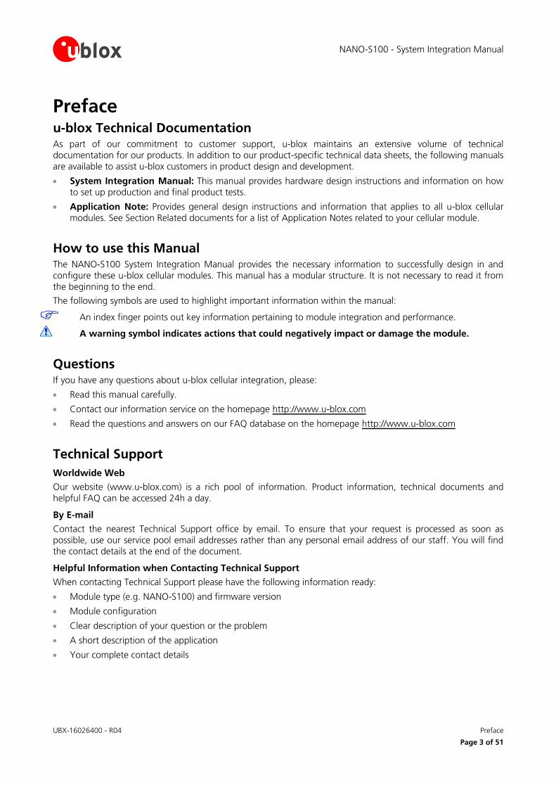
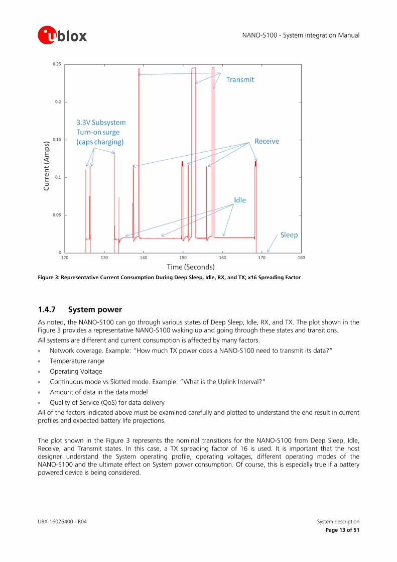
When the NANO-S100 transmits, it uses a variable transmit power that is correlated to its received RSSI. In this state, the NANO-S100 is likely at its highest power states, but this is somewhat dependent on RSSI. Figure 3 shows the worst case state (maximum power). This is at approximately 23.3 dBm output power. This is the highest power state for the NANO-S100.
Time (s)
Sleep
Calibrate
NANO-S100 - System Integration Manual
UBX-16026400 - R04 System description
Page 13 of 51
Figure 3: Representative Current Consumption During Deep Sleep, Idle, RX, and TX; x16 Spreading Factor
1.4.7 System power
As noted, the NANO-S100 can go through various states of Deep Sleep, Idle, RX, and TX. The plot shown in the Figure 3 provides a representative NANO-S100 waking up and going through these states and transitions.
All systems are different and current consumption is affected by many factors.
Network coverage. Example: “How much TX power does a NANO-S100 need to transmit its data?”
Temperature range
Operating Voltage
Continuous mode vs Slotted mode. Example: “What is the Uplink Interval?”
Amount of data in the data model
Quality of Service (QoS) for data delivery
All of the factors indicated above must be examined carefully and plotted to understand the end result in current profiles and expected battery life projections.
The plot shown in the Figure 3 represents the nominal transitions for the NANO-S100 from Deep Sleep, Idle, Receive, and Transmit states. In this case, a TX spreading factor of 16 is used. It is important that the host designer understand the System operating profile, operating voltages, different operating modes of the NANO-S100 and the ultimate effect on System power consumption. Of course, this is especially true if a battery powered device is being considered.

NANO-S100 - System Integration Manual
UBX-16026400 - R04 System description
Page 14 of 51
1.5 Application for power modes
The section describes two major methods of implementing the NANO-S100: Powered and battery operated modes:
Powered Operating mode: “Powered” refers to the host board and its power supply. Specifically, it refers to a good solid, consistent power supply – such as an AC powered source. In this type of usage case, the host can potentially supply a good clean 3.3 V rail (3V3 pin 4) without regard to extreme detail of optimizing power consumption.
Battery Operated mode: This mode refers to a battery operated device in which extreme care and attention is applied to reducing overall power consumption. All details and all modes of power consumption are considered and optimized.
1.5.1 Powered operating mode
In this scenario, the host and module’s power consumption is not really a consideration. In this case, the host can take an input voltage and convert to a 100% duty 3.3 V supply. This would be applied to:
Host CPU
VBATT pin
3V3 pin
In this case, the module will internally turn the 3.3 V rail ON/OFF as it is required. The module attempts to gate this internal supply OFF to conserve power, when it can. The HW status of the 3.3V supply is the WAKE signal (3.3 V = “ON” if WAKE is high). When the 3.3 V is internally gated off, the module consumes virtually no power on that supply.
However, the host CPU is always powered by 3.3 V – the operating level of the host to NANO-S100 SPI interface. The NANO-S100 requires a full 3.3 V during SPI transfers. For a wired example of the Powered circuitry, see the Figure 4.
1.5.2 Battery operated mode
Battery operating mode offers a much more challenging design constraint. The goal is to reduce current consumption where possible. To this conservation goal, see Figure 5 for a Lithium Battery example schematic.
The assumption in this design goal is to use a long life battery such as Lithium battery/cell. These primary cells offer:
Extreme low self-discharge
Long life
Wide operating temperatures
High capacity
2.2 V – 3.6 V direct voltage over the operating temperature and discharge characteristics of the cell

NANO-S100 - System Integration Manual
UBX-16026400 - R04 System description
Page 15 of 51
In this case, assume that:
The VBATT pin of the module is connected directly to the cell (2.2 V – 3.6 V).
The 3V3 signal of the module is connected directly to the 3.3 V regulator. The regulator is turned ON/OFF depending on the state of the WAKE pin of the module.
The CPU uses an indirect path through a dual Schottky diode to permit seamless switching/transition from battery voltage to 3.3 V.
Most modern CPUs used for this type of application have the following characteristics:
o Operate at 1.8 V – 3.6 V
o Low sleep current (1 – 2 µA with full SRAM retention for fast wakeup)
o Pins that use interrupts to wake the processor from deep sleep
The following sections describe the major operating states and power supply modes.
1.5.3 Sleep mode assumptions
1. The module is powered “on” (ON_OFF = high).
2. The module is in sleep mode when in the wake state (WAKE = low).
3. The module is consuming minimal current through its VBATT pin.
4. 3V3 is off and is not required by the host or module.
5. The host CPU can run off the “natural voltage” of the cell only drawing microAmperes of current.
1.5.4 Active mode
If the module is operated in a battery mode, when the 3V3 pin is not always enabled, the 3V3 pin supply must power up and be stable within 2 ms of the WAKE signal going "high".
When the module awakens (WAKE = high) and the 3.3 V power supply is turned “on”:
The module uses the supplied 3.3 V as required.
The 3V3 pin must be on and stable within 2 ms of WAKE being asserted high.
The voltage of the CPU ramps to the higher of the following: cell voltage or 3.3 V supply.
The 3.3 V on the host and the module permits the module to fully function on the RPMA network and also allows host-module SPI communications.
A Texas Instruments TPS63000 3.3V buck/boost regulator (or equivalent) is recommended for NANO-S100 applications. This has some unique benefits:

NANO-S100 - System Integration Manual
UBX-16026400 - R04 System description
Page 16 of 51
When in high efficiency mode (PS/SYNC = low), the regulator outputs a loose 3.3 V with +/-100 mV ripple. In this mode, its quiescent current is only 50 µA.
When in low efficiency (but “clean” output) mode (PS/SYNC = high), the regulator is within +/-20 mV ripple but consumes a 0.6 mA quiescent current.
These operating modes align well with the module’s operating modes as defined by the RF_SHDN pin:
When tight regulation (low ripple) is required by the RF of the module:
o RF_SHDN = high
o PS/SYNC = high
When the module does not need tight regulation and is in a moderately low power mode, RF_SHDN is low (and PS/SYNC is low).
Other design considerations for optimal low power are as follows:
1. Reduce capacitance in the 3.3V domain. Extra capacitors require charging each time the 3.3 V is turned "on".
2. Ensure all software and CPU configurations set CPU pins to low power states. 3. Use high value resistors such as 1 M or greater for pull-ups/pull-downs where possible.

NANO-S100 - System Integration Manual
UBX-16026400 - R04 System description
Page 17 of 51
1.5.5 Example schematics
Figure 4: Example of non-battery “Powered” application schematic
Figure 5: Example of Lithium Battery application schematic

NANO-S100 - System Integration Manual
UBX-16026400 - R04 System description
Page 18 of 51
1.6 SPI interface and sequences
1.6.1 SPI system interface overview
The SPI slave interface is the only supported interface for host-to-module communication. The SPI System interface is controlled / handled by the Host Common Library, compiled onto the user’s apps processor. This section is intended for background informational purposes only.
The NANO-S100 must be the only SPI slave on the bus.
The SPI slave interface provides communication with an external host through a 7-wire interface. The host is the SPI master and the NANO-S100 is the SPI slave. In addition to the four standard SPI signals, three additional signals are used to complement the SPI bus: MRQ, SRQ, and SRDY. The additional signals are included to support NANO-S100 state transitions and bi-directional message traffic.
The SPI signals include four that are controlled by the master and three that are controlled by the slave.
Master-controlled signals (host) Slave-controlled signals (NANO-S100)
MOSI MISIO
SCKL SRQ
CS SRDY
MRQ
Figure 6: SPI signal control between host and module
When MRQ and SRQ are low, the remaining Master controlled signals (MOSI, SCLK, and CS) must be held low or tri-stated. This is to prevent these signals from back-driving the NANO-S100 (Slave) that may be in deep sleep. When either MRQ or SRQ assert high, the Master should set each of the three signals appropriately according to their standard usage. No pull-up resistors should ever be applied to any signals on the NANO-S100 since it often needs to fall into a Deep Sleep mode (all internal regulators turned off).
Figure 7: SPI interface
NANO-S100 - System Integration Manual
UBX-16026400 - R04 System description
Page 19 of 51
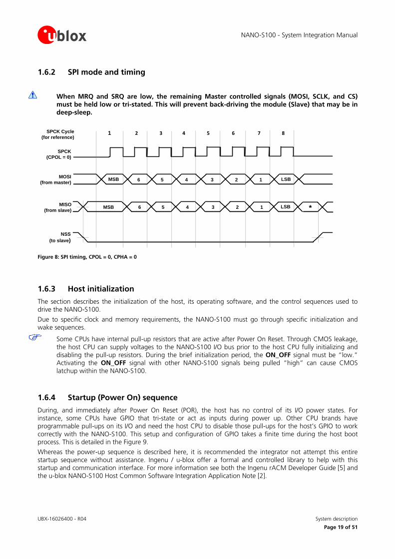
1.6.2 SPI mode and timing
When MRQ and SRQ are low, the remaining Master controlled signals (MOSI, SCLK, and CS) must be held low or tri-stated. This will prevent back-driving the module (Slave) that may be in deep-sleep.
MOSI
(from master)
1
NSS
(to slave)
MISO
(from slave)
SPCK
(CPOL = 0)
2 3 4 5 6 7 8SPCK Cycle
(for reference)
MSB
MSB
LSB
LSB *6 5 4 3 2 1
6 5 4 3 2 1
Figure 8: SPI timing, CPOL = 0, CPHA = 0
1.6.3 Host initialization
The section describes the initialization of the host, its operating software, and the control sequences used to drive the NANO-S100.
Due to specific clock and memory requirements, the NANO-S100 must go through specific initialization and wake sequences.
Some CPUs have internal pull-up resistors that are active after Power On Reset. Through CMOS leakage, the host CPU can supply voltages to the NANO-S100 I/O bus prior to the host CPU fully initializing and disabling the pull-up resistors. During the brief initialization period, the ON_OFF signal must be “low.” Activating the ON_OFF signal with other NANO-S100 signals being pulled “high” can cause CMOS latchup within the NANO-S100.
1.6.4 Startup (Power On) sequence
During, and immediately after Power On Reset (POR), the host has no control of its I/O power states. For instance, some CPUs have GPIO that tri-state or act as inputs during power up. Other CPU brands have programmable pull-ups on its I/O and need the host CPU to disable those pull-ups for the host’s GPIO to work correctly with the NANO-S100. This setup and configuration of GPIO takes a finite time during the host boot process. This is detailed in the Figure 9.
Whereas the power-up sequence is described here, it is recommended the integrator not attempt this entire startup sequence without assistance. Ingenu / u-blox offer a formal and controlled library to help with this startup and communication interface. For more information see both the Ingenu rACM Developer Guide [5] and the u-blox NANO-S100 Host Common Software Integration Application Note [2].

NANO-S100 - System Integration Manual
UBX-16026400 - R04 System description
Page 20 of 51
The initial sequencing of the 3V3 and VBATT rails can be either:
Both 3V3 and VBATT can be applied simultaneously
The VBATT can rise first if 3V3 follows within 1 ms, but the 3V3 should never rise prior to VBATT.
To avoid damage to the module never apply supply to the 3V3 pin prior to VBATT.
The timing sequence shown in Figure 9 is described in detail below. The timing in the Figure 9 is not to scale.
t0 t1: This phase is where the host’s system power has been applied and the host software must power up and initialize the GPIO interfaces for the NANO-S100 to the required states defined at time t1. The t1 state becomes “TRUE” indicating the host sets all the GPIO to a known and controlled state (Low).
t2: At t2 state, all the output signals to the NANO-S100 are set low and the Power On Signal is set high. This turns on the internal LDO regulators of the NANO-S100 to initiate a power up sequence. The time between t1-t2: is approximately 100 ms, or longer. Assert ON_OFF “high” starts an internal clock (32 kHz) and releases an internal reset pin which may take up to 3 seconds to stabilize.
t3: t3 is when the host releases the NANO-S100 from its Reset state. This time allows the 32 kHz of the NANO-S100 to turn on and stabilize. The time between t2-t3 is 1 s, or longer.
t4: t4 signals the start of the host wanting to initiate communications (arbitration) with the NANO-S100. The host raises MRQ to turn on various circuitries. The time between t3-t4 is 10 ms, or longer.
t5: After the assertion of t4, the NANO-S100 begins its “wake sequence.” The NANO-S100 must boot, initialize its operating system and hardware and when it is ready for communications it raises its SRDY signal back to the host. At this point, communications (Arbitration) can begin.
t6: At this point the NANO-S100 signals its readiness by asserting the SRDY pin. The host can now begin communications with the NANO-S100.
t0 t1 t2 t3 t4 t5 t6
3000 ms 10 ms 4 ms
t6 – t4 < 300 ms or error
SRDY
SPI
System
MRQ
Int Node
Reset/Init
(not a signal)
Power On
Host Init
(not a signal)
3.3V/VBATT
Hi-Z
100 ms
*Note: timing shown not to scale
Figure 9: NANO-S100 Power-up Timing Sequence
NANO-S100 - System Integration Manual
UBX-16026400 - R04 System description
Page 21 of 51
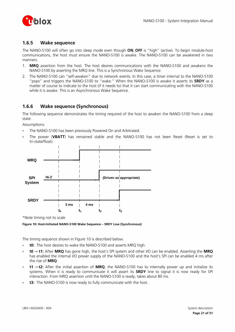
1.6.5 Wake sequence
The NANO-S100 will often go into sleep mode even though ON_OFF is “high” (active). To begin module-host communications, the host must ensure the NANO-S100 is awake. The NANO-S100 can be awakened in two manners:
1. MRQ assertion from the host. The host desires communications with the NANO-S100 and awakens the NANO-S100 by asserting the MRQ line. This is a Synchronous Wake Sequence.
2. The NANO-S100 can “self-awaken” due to network events. In this case, a timer internal to the NANO-S100 “pops” and triggers the NANO-S100 to “wake.” When the NANO-S100 is awake it asserts its SRDY as a matter of course to indicate to the host (if it needs to) that it can start communicating with the NANO-S100 while it is awake. This is an Asynchronous Wake Sequence.
1.6.6 Wake sequence (Synchronous)
The following sequence demonstrates the timing required of the host to awaken the NANO-S100 from a sleep state.
Assumptions:
The NANO-S100 has been previously Powered On and Arbitrated.
The power (VBATT) has remained stable and the NANO-S100 has not been Reset (Reset is set to tri-state/float).
t0 t1 t2 t3
SRDY
SPI
System
MRQ
Hi-Z
4 ms
(Driven as appropriate)
3 ms
*Note timing not to scale
Figure 10: Host-Initiated NANO-S100 Wake Sequence – SRDY Low (Synchronous)
The timing sequence shown in Figure 10 is described below.
t0: The host desires to wake the NANO-S100 and asserts MRQ high.
t0 t1: After MRQ has gone high, the host’s SPI system and other I/O can be enabled. Asserting the MRQ has enabled the internal I/O power supply of the NANO-S100 and the host’s SPI can be enabled 4 ms after the rise of MRQ.
t1 t2: After the initial assertion of MRQ, the NANO-S100 has to internally power up and initialize its systems. When it is ready to communicate it will assert its SRDY line to signal it is now ready for SPI interaction. From MRQ assertion until the NANO-S100 is ready, takes about 80 ms.
t3: The NANO-S100 is now ready to fully communicate with the host.

NANO-S100 - System Integration Manual
UBX-16026400 - R04 System description
Page 22 of 51
1.6.7 Wake sequence (Asynchronous)
In this scenario, the NANO-S100 is already awake due to a networking event (SRDY is already high) and the host wants to communicate with the NANO-S100 while it is awake. The host asserts MRQ to ensure that the NANO-S100 stays awake during its communication cycle.
t0 t1 t2 t3
SRDY
SPI
System
MRQ
Hi-Z (Driven as appropriate)
< 250 μs
*Note timing not to scale
Figure 11: Host-Initiated NANO-S100 Wake Sequence – SRDY high (asynchronous)
1.6.8 Host-Driven reset sequence
If the NANO-S100 fails to communicate (or similar), it may be necessary to “Reset” the NANO-S100. Figure 12 shows the proper sequence to reset the device. Resetting the device causes it to go through an RPMA Cold Acquisition process to reacquire the network.
ON_OFF
t0 t1 t2 t3 t4 t5 t6
3000 ms 10 ms 4 ms
SRDY
SPI
System
MRQ
VBATT
Hi-Z
15 ms
(Driven as appropriate)
*Note timing not to scale
Figure 12: Host-Driven Reset Sequence

NANO-S100 - System Integration Manual
UBX-16026400 - R04 System description
Page 23 of 51
1.6.9 Host MRQ release / NANO-S100 allowed to sleep sequence
If the host determines there are no more messages or SPI transactions required, it nominally de-asserts the MRQ to allow the NANO-S100 to fall back to Deep Sleep (lowest power mode). Figure 13 shows how this is sequenced by the host/NANO-S100. A small delay in de-asserting SRDY is enforced to prevent quick toggling (waking) of the NANO-S100.
t0 t1 t2
SRDY
SPI
System
MRQ
Hi-Z
10 ms3 ms
*Note timing not to scale
Figure 13: Host MRQ Release/NANO-S100 Allowed to Sleep Sequence
1.7 SPI messaging protocol
The SPI messaging between the host processor and the module is controlled / handled by the Host Common Library, compiled onto the user’s apps processor. This section are intended for background informational purposes only.
The details of host/module messaging are typically not necessary for integrators to implement. The rACM application code is a working example of a host common integration on an NXP (formerly Freescale) K20.
1.7.1 Arbitration
Arbitration is the process a host uses to signal to the module that it supports the bi-directional messaging protocol. The arbitration sequence is designed to reduce the probability that an arbitrary non-host transfer sequence can mirror a valid arbitration sequence.
Arbitration consists of both host and module transmitting an arbitration request/reply pair. After a defined turn-around delay, both transmit a validation request/reply. The turn-around delay avoids race conditions between host and module and provides enough time to allow ISR execution to complete before the next SPI transfer.
If the module does not reply to the host request, the host needs to wait for a turn-around delay and retry the arbitration request.
The host must perform the arbitration sequence before any other SPI bus communication can take place between the host and the module.
The host must initiate this arbitration sequence on boot-up. Additionally, the host must perform the arbitration sequence when the module sends to the host an arbitration message. This can occur due to the module going into Deep Sleep and then waking up. Since the module requires the arbitration sequence after waking from Deep Sleep and since the host is not aware of when the module goes to Deep Sleep, the host must be able to detect that the module is requesting arbitration and the host must then reset its host interface state machine and perform arbitration. For more information on the host interface SPI bus state machine, see the section 1.7.3.

NANO-S100 - System Integration Manual
UBX-16026400 - R04 System description
Page 24 of 51
1.7.2 Message protocol
Host-to-module transfers use master message command pairs and module-to-host transfers use slave message command pairs. Both transfers use identical command sequences with only the encoding of the commands differing. The command sequence for a message transfer consists of a request/acknowledgement pair followed by a defined turn-around delay and then a message composed of a header pair and a payload.
Variable length payloads are supported by encoding the payload size in the second half of the message request. The second half of the message reply contains the available receive buffer size. If the message payload size exceeds the receive buffer size, then a new request must be made after a turn-around delay with a payload size that does not exceed the receive buffer size.
After a successful message request transfer, the host waits a turn-around delay and then initiates the transfer with a message header command. The payload immediately follows the header and, if necessary, is zero padded to match the payload size indicated in the message request. After the payload, the host waits a turn-around delay before proceeding with any other further messages.
The host interface SPI bus is a standard SPI bus (with MISO, MOSI, CS, and SCLK) with the addition of three lines (MRQ, SRQ, and SRDY). These three additional lines are used to provide the host with the ability to wake up the module over the SPI Bus as well as providing the module with the ability to prompt the host to begin a SPI Bus transaction. The module is also exceptional in that it must be the only slave present on the SPI Bus, since MOSI, CS, and SCLK must be undriven (tri-stated) any time that MRQ is low.
Before any message is communicated over the SPI Bus, the MRQ and SRDY lines must be high. The host guarantees this by pulling the MRQ line high and waiting for the module to pull the SRDY line high. The host cannot proceed with SPI Bus communication until both of these lines are high. Once MRQ and SRDY are high, the host, being SPI Bus master, can continue with a normal SPI Bus transaction.
When the module wishes to communicate with the host, it pulls the SRQ line high. The host must have the ability to detect this and start a SPI Bus transaction (by first pulling the MRQ high and waiting for SRDY to go high). A standard SPI Bus transaction is described and illustrated in Figure 16.
Message exchanges between host and module are shown below in Figure 14.
In each of the request/acknowledge command pairs shown, the top command is transmitted by the host (master) and the bottom command is transmitted by the module (slave). The wait bubbles indicate a predefined turn-around delay which provides ISR processing time and avoids race conditions between host and module.

NANO-S100 - System Integration Manual
UBX-16026400 - R04 System description
Page 25 of 51
MRQ=1
Node
SRDY=1
HostSlave
Request
Slave Ready
ArbREQ
ArbACK
ValREQ
ValACK
Arbitration
Request
Arbitration
Acknowledge
Validation
Acknowledge
Validation
Request
MMsgREQ+Size
MMsgACK+Size
MHdrREQ
MHdrACK
Master Message
Request
Master Message
Acknowledge
Master Header
Request
Master Header
Acknowledge
Payload
Transmit
Payload
Receive
SMsgREQ+Size
SMsgACK+Size
SHdrREQ
SHdrACK
Slave Message
Request
Slave Message
Acknowledge
Slave Header
Request
Slave Header
Acknowledge
Payload
Transmit
Payload
Receive
Repeat 6 steps above
PAYLOAD
SRQ=1Slave
Request
Arbitration
Host-to- Node
Message
Transfer
Node-to-Host
Message
Transfer
wait
wait
wait
wait
wait
wait
wait = Turn-around Delay
MRQ=1
SRDY=1
MRQ=1
SRDY=1
wait
wait
PAYLOAD
Repeat 5 steps above
if needed
Figure 14: SPI Master and Slave Message Sequences
NANO-S100 - System Integration Manual
UBX-16026400 - R04 System description
Page 26 of 51
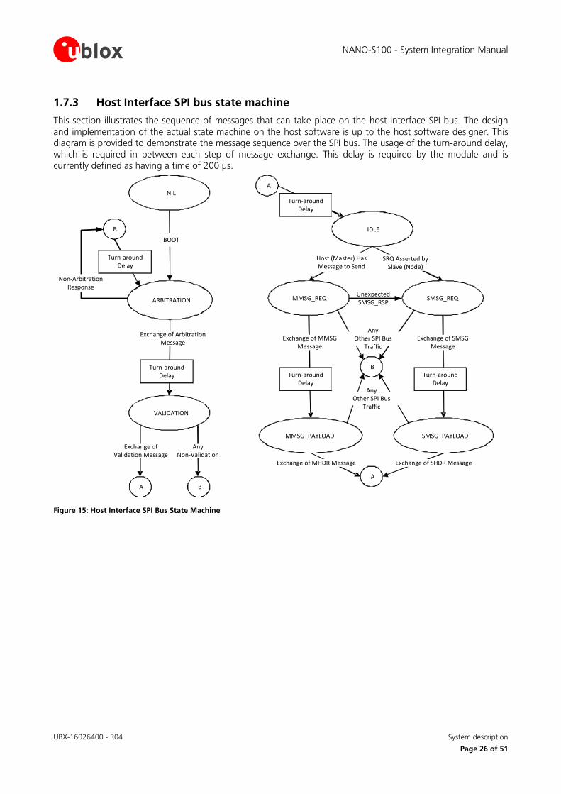
1.7.3 Host Interface SPI bus state machine
This section illustrates the sequence of messages that can take place on the host interface SPI bus. The design and implementation of the actual state machine on the host software is up to the host software designer. This diagram is provided to demonstrate the message sequence over the SPI bus. The usage of the turn-around delay, which is required in between each step of message exchange. This delay is required by the module and is currently defined as having a time of 200 µs.
ARBITRATION
NIL
VALIDATION
IDLE
MMSG_REQ SMSG_REQ
MMSG_PAYLOAD SMSG_PAYLOAD
A
A
B
B
Turn-around Delay
A
Turn-around Delay
Turn-around Delay
Turn-around Delay
Turn-around Delay
B
BOOT
Exchange of Arbitration Message
Exchange of Validation Message
AnyNon-Validation
Exchange of MHDR Message Exchange of SHDR Message
Exchange of MMSG Message
AnyOther SPI Bus
Traffic
AnyOther SPI Bus
Traffic
Exchange of SMSG Message
Host (Master) Has Message to Send
SRQ Asserted by Slave (Node)
Non-Arbitration Response
Unexpected SMSG_RSP
Figure 15: Host Interface SPI Bus State Machine

NANO-S100 - System Integration Manual
UBX-16026400 - R04 System description
Page 27 of 51
1.7.4 SPI bus timing example
This section provides an example illustration of an exchange of messages first from master (host) to slave (module) and then from slave (module) to master (host). Each step in the timing sequence is described below:
SRQ
MRQ
SRDY
CS
SCLK
MISO
MOSI
6
9
5 10
11
1
2
3 4 7 8
Figure 16: SPI timing example
MRQ state transitions must respect the timing requirements section and sub-sections of 1.6.
The following items pertain to the numbered bubbles above:
1. Host has a message that it desires to send to module. The first thing that it does is drive MRQ and CS high. 2. The host then waits for the module to drive SRDY high. No SPI bus transaction with the module can occur
before this. 3. After SRDY is high, the host can start with the SPI data transaction. This is accomplished by driving the
module CS line low and then having the host toggle the SCLK, and MOSI lines and having the module toggle the MISO line according to the data to be transferred. The SPI host interface specifies that first a MMsg pair is exchanged.
4. A MHdr pair is exchanged. Note that the payload of the message is appended to the MHdr. 5. The host detects that the transaction is complete and that it does not wish to send more messages to the
module at this time. It drives the MRQ line low. Since MRQ is low, CS, SCLK and MOSI are tri-stated. 6. At some time in the future, the module desires to send a message to the host. It indicates this to the host by
driving SRQ high. Since SRQ is high, the host drives MRQ and then CS high. It then waits for SRDY to go high, which it already is.
7. The host starts the SPI data transaction. This is accomplished by driving the module CS line low and then having the host toggle the SCLK, and MOSI lines and having the module toggle the MISO line according to the data to be transferred. The SPI host interface specifies that first a SMsg pair is exchanged.
8. A SHdr pair is exchanged. Note that the payload of the message is appended to the SHdr. 9. The module detects that the transaction is complete and that it does not wish to send more messages to the
host at this time. It drives the SRQ line low. 10. The host detects that SRQ has gone low and that it does not have any messages to send to the module. It
drives the MRQ line low. Since MRQ is low, CS, SCLK and MOSI are tri-stated. 11. The module drives the SRDY line low after MRQ goes low.

NANO-S100 - System Integration Manual
UBX-16026400 - R04 System description
Page 28 of 51
1.7.5 Host message SPI example
This section provides an example host message exchange from master (host) to slave (module). In this example, the host is sending a version request message.
This example is a zoomed-in view of the example provided previously in Figure 16. This section covers what happens in step 3 of the example, which includes the two SPI exchanges initiated by the host.
With any SPI host interface message, first an MMsg or SMsg pair must be exchanged. This pair contains information on how big the message is (from the message originator) and how much message queue space is available (on the message destination).
The following diagram in Figure 17 shows such an example.
SCLK
MISO
MOSI
0 1 1 0 1 0 0 1 1 1 1 1 1 1 1 1
1 0 1 0 1 0 0 1 1 0 0 0 0 0 0 0
Figure 17: Host Message on SPI – MMsg Pair
The SPI clock edging is configurable with a polarity and phase. In order to communicate with the module, the SPI clock polarity must be set to “the inactive state value of SPI clock is logic level zero” and the SPI clock phase must be set to “data is captured on the leading edge of SPI clock and changed on the following edge of SPI clock.” This means that the data lines (both MISO and MOSI) are read on the SCLK rising edge and are set or cleared on the SCLK falling edge, and is commonly referred to as CPOL=0, CPHA=0.
This illustration shows that the bit streams for MISO and MOSI are:
MISO: 0110100111111111
MOSI: 1010100100000100
These bits indicate:
MISO
from slave to master (01)
length of message=2 (10)
opcode=MMsgACK (1001)
buffer size=255 (11111111)
MOSI
from master to slave (10)
length of message=2 (10)
opcode =MMsgREQ (1001)
payload size=4 (00000100)
NANO-S100 - System Integration Manual
UBX-16026400 - R04 System description
Page 29 of 51
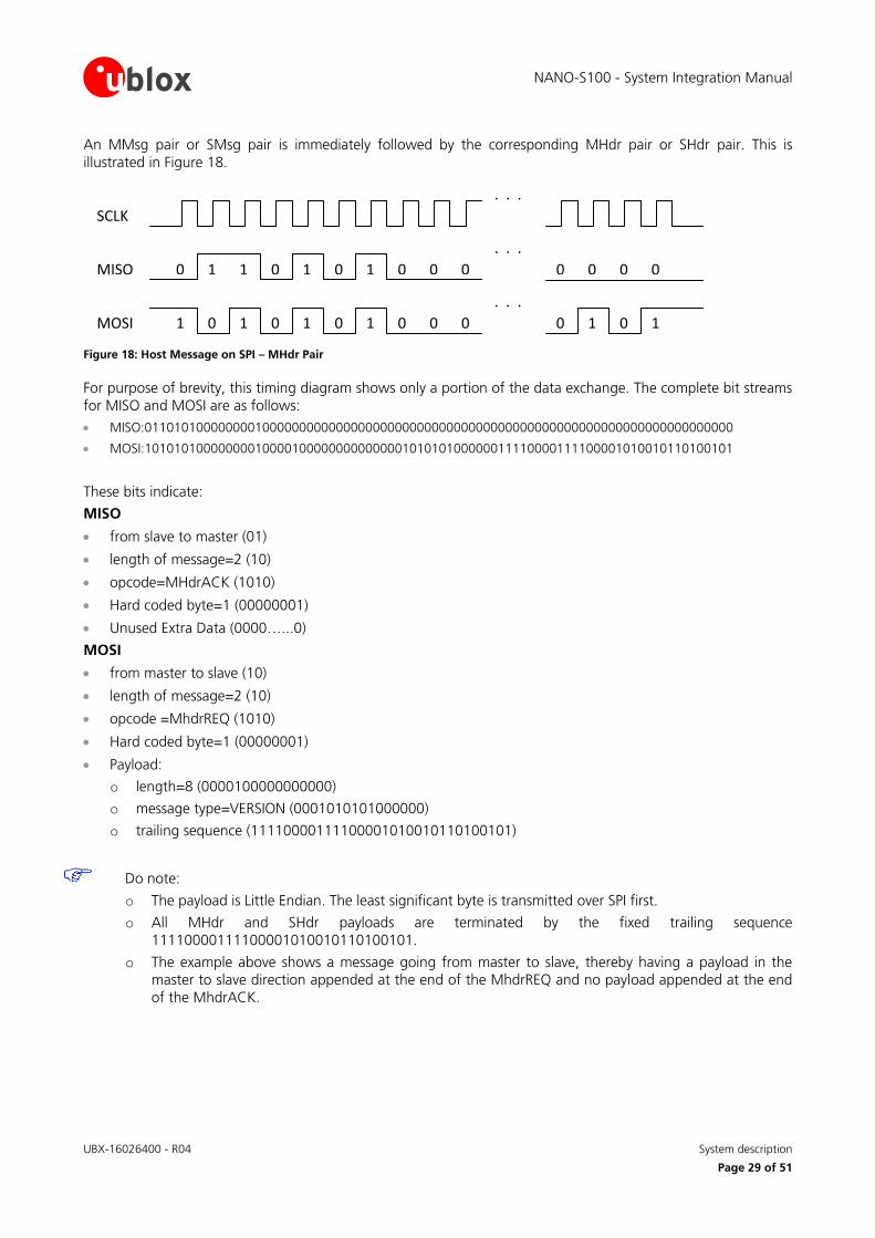
An MMsg pair or SMsg pair is immediately followed by the corresponding MHdr pair or SHdr pair. This is illustrated in Figure 18.
SCLK
MISO
MOSI
. . .
0 1 1 0 1 0 1 0 0 0
1 0 1 0 1 0 1 0 0 0
. . .
. . .
0 1 0 1
0 0 0 0
Figure 18: Host Message on SPI – MHdr Pair
For purpose of brevity, this timing diagram shows only a portion of the data exchange. The complete bit streams for MISO and MOSI are as follows:
MISO:01101010000000010000000000000000000000000000000000000000000000000000000000000000
MOSI:10101010000000010000100000000000000101010100000011110000111100001010010110100101
These bits indicate:
MISO
from slave to master (01)
length of message=2 (10)
opcode=MHdrACK (1010)
Hard coded byte=1 (00000001)
Unused Extra Data (0000…...0)
MOSI
from master to slave (10)
length of message=2 (10)
opcode =MhdrREQ (1010)
Hard coded byte=1 (00000001)
Payload:
o length=8 (0000100000000000)
o message type=VERSION (0001010101000000)
o trailing sequence (11110000111100001010010110100101)
Do note:
o The payload is Little Endian. The least significant byte is transmitted over SPI first.
o All MHdr and SHdr payloads are terminated by the fixed trailing sequence 11110000111100001010010110100101.
o The example above shows a message going from master to slave, thereby having a payload in the master to slave direction appended at the end of the MhdrREQ and no payload appended at the end of the MhdrACK.

NANO-S100 - System Integration Manual
UBX-16026400 - R04 System description
Page 30 of 51
1.7.6 Host message “Connect” SPI example
This section provides an example host message exchange of the CONNECT message from master/host to slave/module and subsequent response from the slave to the master.
The timing is similar to the timing illustrated in the previous section, but the data and length of data is different.
The steps involved in this exchange are as follows:
The host desires to send the CONNECT message to the module. As described in the previous section, this starts with an MmsgREQ/MmsgACK exchange over the SPI bus.
MISO: 0110100111111111
MOSI: 1010100100000110
These bits indicate:
MISO:
from slave to master (01)
length of message=2 (10)
opcode=MMsgACK (1001)
buffer size=255 (11111111)
MOSI:
from master to slave (10)
length of message=2 (10)
opcode =MmsgREQ (1001)
payload size=6 (00000110)
The MMsg exchange is followed by the MHdr exchange, which includes the payload of the CONNECT message.
MISO: 0110101000000001000000000000000000000000000000000000000000000000000000000000000000000000000000000000000000000000
MOSI: 1010101000000001000011000000000000110010010000000000000100000000000000000000000011110000111100001010010110100101
These bits indicate:
MISO:
from slave to master (01)
length of message=2 (10)
opcode=MHdrACK (1010)
Hard coded byte=1 (00000001)
Unused Extra Data (0000…...0)
MOSI:
from master to slave (10)
length of message=2 (10)
opcode=MhdrREQ (1010)
Hard coded byte=1 (00000001)
Payload:
o length=12 (0000110000000000) o message type=CONNECT (0011001001000000) o host interface=True (00000001000000000000000000000000) o trailing sequence (11110000111100001010010110100101)

NANO-S100 - System Integration Manual
UBX-16026400 - R04 System description
Page 31 of 51
The payload of the message includes first the length, which is the number of bytes in the payload including the length and the trailing sequence.
It is followed by the message type, which in this case is 0x4032, and corresponds with CONNECT.
The CONNECT message has a 4-byte field that is a Boolean flag specifying whether or not the module should send asynchronous SPI messages to the host. To specify that the module should send messages to the host, the value of 0x00000001 is used.
It is then followed by the standard fixed trailing sequence.
This message exchange is followed by a module-initiated message exchange for the purpose of sending an ACK of the CONNECT message to the host. This starts with a SmsgREQ/SMsgACK exchange over the SPI bus.
MISO: 0110101100000100
MOSI: 1010101111111111
These bits indicate:
MISO:
from slave to master (01)
length of message=2 (10)
opcode=SMsgACK (1011)
buffer size=255 (11111111)
payload size=4 (00000100)
MOSI:
from master to slave (10)
length of message=2 (10)
opcode =SmsgREQ (1011)
buffer size=255 (11111111)
The SMsg exchange is followed by the SHdr exchange, which includes the payload of the ACK message.
MISO: 01101100000000010000100000000000001100000000000011110000111100001010010110100101
MOSI: 10101100000000010000000000000000000000000000000000000000000000000000000000000000
These bits indicate:
MISO:
from slave to master (01)
length of message=2 (10)
opcode=SHdrACK (1100)
Hard coded byte=1 (00000001)
Payload:
o length=8 (0000100000000000)
o message type=ACK (0011000000000000)
o trailing sequence (11110000111100001010010110100101)
MOSI:
from master to slave (10)
length of message=2 (10)
opcode =ShdrREQ (1100)
Hard coded byte=1 (00000001)
Unused Extra Data (0000…...0)

NANO-S100 - System Integration Manual
UBX-16026400 - R04 System description
Page 32 of 51
1.8 RF connection
The ANT1 and ANT2 pads each have a 50 nominal characteristic impedance and must be connected to the
antenna through a 50 transmission line to allow transmission and reception of radio frequency (RF) signals in the ISM operating bands
Name Description Remarks
NANO-S100 ANT1 ANT2 Surface Mount pad with Zo = 50 nominal characteristic impedance.
Table 4: Antenna connectivity
Choose an antenna with optimal radiating characteristics for the best electrical performance and overall module functionality. Focus on minimizing the insertion loss between radiating antenna and the module RF connector. See section 2.3 for further details regarding antenna guidelines.
See section 2.5 for details on antennae used for NANO-S100 certification.
1.8.1 RF diversity
Through ANT2 pin, the NANO-S100 supports Antenna Diversity for optimal system performance. In many cases, the NANO-S100 and host system are mounted in fixed locations that often experience nulls in the RF coverage. Antenna Diversity can help with optimization of the RX and TX links. In marginal coverage areas, an RF null could easily disadvantage the NANO-S100 to force it to transmit at a higher TX Power (more battery energy) or cause network loss and frequent rescanning to reacquire the network (again, more energy). In summary, diversity potentially provides:
High link reliability
Better pattern coverage; less nulls
Better ability to see more AP to connect to
Lower power consumption

NANO-S100 - System Integration Manual
UBX-16026400 - R04 System description
Page 33 of 51
1.8.2 Example antenna circuit
Figure 19: Example antennae implementation with Ethertronics 1001013 antenna
1.9 RF interference and channels to avoid
The NANO-S100 uses a channel scheme such as the following:
Channel 1 = 2402 MHz and each successive channel is 1.99 MHz offset to that Channel 1.
Channel 2 = 2403.99 MHz
Channel 3 = 2405.98 MHz
Etc.
The NANO-S100 uses a 26 MHz reference clock for processing and for the direct conversion radio. It has been found that 26 MHz harmonics can create strong tones that cause some RF sensitivity degradation on these harmonic channels.
93*26 MHz = 2418 MHz. This affects channel 9.
94*26 MHz = 2444 MHz. This affects channel 22.
95*26 MHz = 2470 MHz. This affects channel 35.
System integrators should NOT use these 3 channels, because NANO-S100 RX sensitivity can be degraded by a nominal 3-10 dB.
ANT1
ANT2

NANO-S100 - System Integration Manual
UBX-16026400 - R04 System description
Page 34 of 51
1.10 Reserved pins (RSVD)
The NANO-S100 module has pins reserved. See the NANO-S100 Data Sheet [1] for the list of NANO-S100 reserved pins and connectivity guidelines.
1.11 Approvals
The NANO-S100 is designed to meet regulations for world-wide use. It is certified in the United States, Canada, and Europe as a Limited Single Module. Table 5 lists the certifications currently achieved.
Country Certifying Agency Certifications
US Federal Communications
Commission (FCC)
FCC 47 CFR Part 15, Subpart C, Clause 15.247 for RF TX bandwidth, power,
conducted and radiated emissions.
Canada Industry Canada (IC) RSS247 Issue 1 and RSS-GEN Issue 4. This includes FCC tests and ISED-specific tests
(RX radiated emissions).
Europe European Telecommunications
Standards Institute ETSI ETSI EN 300 440-1 and 440-2, ETSI Emissions.
301 489-1, ETSI Immunity.
Table 5: NANO-S100 certifications
Additional details can be found in the document by Ingenu EMC Compliance Guide [6].
The integrator of the final product is often required to do additional compliance tests. The integration application and market will determine specifics. The integrator is advised to consult with local experts in compliance certifications for complete information.
1.11.1.1 FCC/ISED
The NANO-S100 is Single-Modular Certified, therefore the final product may only need Class B unintentional radiator and powerline conducted emissions tests. This should be done with the actual production antenna and power supply.
Customers are free to follow one of three paths in their final product evaluations:
Class I permissive change: Customers can use one of Ingenu / u-blox approved antenna types that are of equal and lesser gain along with the antenna PCB reference designs. This path allows customers to use NANO-S100 certification. While ideal from the perspective of program cost and schedule, the ability to reuse this antenna is highly dependent on the application. See section 2.5 for antennas used for NANO-S100 certification.
Class II Permissive change: If there are minor changes when integrating the module and application with the FCC or ISED the NANO-S100 certification can still be used. These changes could be a higher antenna gain, different PCB characteristics, or collocated transmitters as an example. In the case of FCC/IC EMC certifications, if a different antenna type or higher gain antenna is used, it is required that the final product be recertified with the NANO-S100.
New FCC ID: Customers can obtain a new FCC ID for their product with the u-blox approved modules. In this case it is up to the manufacturer of the host equipment to arrange certification.
Customers opting to re-certify on their own with different layout, stack-ups, and antennas, etc., it is important that the NANO-S100 is presented with a 50Ω load. To that end, it is strongly recommended that the RF trace from the NANO-S100 to the antenna be outfitted with a Pi network, near the antenna, for matching during the development phase of a host board.

NANO-S100 - System Integration Manual
UBX-16026400 - R04 System description
Page 35 of 51
1.11.1.2 ETSI
Europe’s system is a self-declaration system. There are no documents to submit or certification grants to obtain. One must have the passing test results available for all applicable requirements at any time if challenged. The NANO-S100 has been verified and qualified for two operational scenarios under EN 300 440-1:
Generic with a maximum of 10 dBm EIRP (2402 – 2475.63 MHz)
Annex C.1 with a maximum of 27 dBm EIRP (2447 – 2452.94 MHz)
The actual minimum/maximum channel frequencies are shown in Table 6.
Module Minimum/Maximum channel frequencies
NANO-S100 2447-2452.94 MHz
Table 6: NANO-S100 Minimum/Maximum Channel Frequencies for Annex C.1 Applications
Other countries will vary.
1.11.2 FCC warnings
This device complies with part 15 of the Federal Communications Commission (FCC) Rules. Operation is subject to the following two conditions:
1. This device may not cause harmful interference.
2. This device must accept any interference received, including interference that may cause undesired operation.
Changes or modifications not expressly approved by the manufacturer could void the user’s authority to operate the equipment.
This equipment has been tested and found to comply with the limits for a Class B digital device, pursuant to Part 15 of the FCC Rules. These limits are designed to provide reasonable protection against harmful interference in a residential installation.
This equipment generates, uses, and can radiate radio frequency energy. If not installed and used in accordance with the instructions, this equipment may cause harmful interference to radio communications. However, there is no guarantee that interference will not occur in a particular installation. If this equipment does cause harmful interference to radio or television reception, which can be determined by turning the equipment off and on, the user is encouraged to try to correct the interference by one or more of the following measures:
Re-orient or relocate the receiving antenna.
Increase the separation between the equipment and receiver.
Connect the equipment into an outlet on a circuit different from that to which the receiver is connected.
Consult the dealer or an experienced radio/TV technician for help.

NANO-S100 - System Integration Manual
UBX-16026400 - R04 System description
Page 36 of 51
1.11.3 ISED warnings
CAN ICES-3 (B)/NMB-3(B)
Canadian Two Part Warning Statement:
The installer of this radio equipment must ensure that the antenna is located or pointed so that it does not emit RF field in excess of Health Canada limits for the general population. Consult Safety Code 6 which is obtainable from Health Canada’s website http://www.hc-sc.gc.ca/index-eng.php.
This device complies with Innovation, Science and Economic Development (ISED) licence-exempt RSS standard(s). Operation is subject to the following two conditions:
1. this device may not cause interference, and 2. this device must accept any interference, including interference that may cause undesired operation of the
device.
To reduce potential radio interference to other users, select the antenna type and its gain so that the equivalent isotropically radiated power (EIRP) is not more than that permitted for successful communication.
L'installateur de cet équipement de radio doit veiller à ce que l'antenne est située ou est pointée de façon à ne pas dégager de champ RF dépassant les limites de Santé Canada pour la population générale. Consulter le Code de sécurité 6 qui peut être obtenu sur le site Web de Santé Canada http://www.hc-sc.gc.ca/index-eng.php
Cet appareil se conforme aux Cahiers des charges sur les Normes Radioélectriques (CNR) d'Industrie Canada applicables aux appareils de radio exempté de licence. Son fonctionnement se soumis aux deux conditions suivantes :
(1) l'appareil ne doit pas produire d’ interférences, et
(2) l'utilisateur de l'appareil doit accepter tout interférences radioélectrique subi, même si les interférences sont susceptible d'en compromettre le fonctionnement.
Pour réduire les interférences radioélectrique pour les autres utilisateurs, sélectionnez le type d'antenne et son gain de sorte que la puissance isotrope rayonnée équivalente (PIRE) ne soit pas supérieure à celle permise pour réussir une communication.
Canada, Industry Canada (IC) Notices
Changes or modifications not expressly approved by the party responsible for compliance could void the user's authority to operate the equipment.
Canada, avis d'Industrie Canada (IC)
Les changements ou modifications n'ont pas était expressément approuvés par la partie responsable de la conformité, ils pourraient annulée l'autorité de l'utilisateur pour exploiter l'équipement.
1.11.4 ETSI warnings
This equipment complies with the essential requirements of the European Union Radio Equipment Directive (RED) 2014/53/EU and the Restriction of Hazardous Substances Directive (RoHS) directive 2011/65/EU.
The NODE103 has been tested against the requirements for both Generic Short Range Devices and Radio Frequency Identification (RFID) according to EN 300 440. Restrictions for RFID performance follow ERC/REC 70-03, Edition May 27, 2016.
It is the responsibility of the integrator to comply by the rules and regulations as outlined in the applicable European directives.

NANO-S100 - System Integration Manual
UBX-16026400 - R04 System description
Page 37 of 51
1.11.5 Usage
This device is only authorized for use in fixed and mobile applications. This device cannot be collocated with other wireless transmitters without performing simultaneous transmission evaluation.
NANO-S100 RF certification IDs:
FCC: XPY2DXMNNN1N
IC: 8595A-2DXMNNN1N
1.11.6 Product labels
If the NANO-S100 is visible in a product, the label showing the FCC ID and IC designators (listed above) must be visible from the exterior of the product.
If the NANO-S100 is contained within a product and is not visible, a label showing the FCC ID and IC designators (listed above) must be affixed to the exterior of the device containing the NANO-S100. The exterior label must state the following:
Contains FCC ID: XPY2DXMNNN1N, IC: 8595A-2DXMNNN1N
1.11.7 RF exposure statement
The air interface supports operation on channels in the 2402 MHz –2475.63 MHz range for FCC/IC and ETSI regulatory domains. Before the NANO-S100 becomes operational, it must undergo a Provisioning procedure, during which critical information required for operation is entered into the device and stored in non-volatile storage. It is during the initial commissioning procedure that the regulatory domain, under which the device will operate, is set. Subsequent configuration of the device during operation is checked against the commissioned regulatory domain and non-permitted channels or transmit power levels are rejected and the device will not transmit until a permissible configuration per the commissioned regulatory domain is set.
1.11.8 WEEE directive
The Waste Electrical and Electronic Equipment (WEEE) directives do not apply to NANO-S100s as they are not considered “end products” that would put them under the WEEE initiatives in the EU.
1.11.9 REACH directive
The NANO-S100s are Registration, Evaluation, Authorization and Restriction of Chemicals (REACH) compliant under 1907/2006/EC. This certification is located in Appendix D.
1.11.10 RoHS directive
The NANO-S100s comply with Restriction of Hazardous Substances Directive (RoHS) directive 2011/65/EU. u-blox has received a Certificate of Conformance (CoC) from Flextronics (contract manufacturer) for all components and printed circuit boards for the NANO-S100s.
1.11.11 Export compliance
The NANO-S100 complies with the export requirements of the Bureau of Industry and Security and relevant information is provided below. For details relating to export compliance for the NANO-S100, see the CCATS numbers provided in Table 7.
ECCN CCATS
ECCN 5A002a.1 G164372
Table 7: ECCN and CCATS Information

NANO-S100 - System Integration Manual
UBX-16026400 - R04 Design-In
Page 38 of 51
2 Design-In
2.1 Design-in checklist
2.1.1 Schematic checklist
The following are the most important points for a simple schematic check:
DC supply must provide a nominal voltage at 3V3 pin above the minimum operating range limit.
DC supply must be capable of supporting 0.36 A, providing a voltage at 3V3 pin above the minimum operating range limit.
3V3 supply should be clean, with very low ripple/noise: suggested passive filtering parts can be inserted. Ripple should be +/- 100mV in high efficiency mode and +/- 20mV in low efficiency mode (see section 1.5.4 for details).
Connect only one DC supply to 3V3: different DC supply systems are mutually exclusive.
Check that voltage level of any connected pin does not exceed the relative operating range.
Provide appropriate access to SPI signal MOSI, MISO, SCLK, CS, MRQ, SRDY and SRQ lines for debugging. Test points are strongly recommended.
Provide proper precautions for ESD immunity as required on the application board.
RSVD pin is left unconnected.
2.1.2 Layout checklist
The following are the most important points for a simple layout check:
Check 50 nominal characteristic impedance of the RF transmission line connected to ANT1 and ANT2 pins to antenna connector or antennae.
Follow the recommendations of the antenna producer for correct antenna installation and deployment.
3V3 line should be wide and short.
Ensure proper grounding and return paths.
Consider “No-routing” areas for the module footprint. See section 2.2.4 for details.
Optimize placement for minimum length of RF line and closer path from DC source for 3V3.
In the stack up make the top and bottom layers ground layers and route all signals in within them to minimize EMI/EMC issues.
2.1.3 Antenna checklist
Antenna should have 50 impedance, V.S.W.R less than 2:1 on operating 2.4 GHz ISM band.
Follow the recommendations of the antenna producer for correct antenna installation and deployment (PCB layout and matching circuitry).
Provide pads to near antenna for matching during development phase, such as a Pi network.

NANO-S100 - System Integration Manual
UBX-16026400 - R04 Design-In
Page 39 of 51
2.2 Design guidelines
The following design guidelines must be met for the optimal integration of NANO-S100 module on the final application board.
2.2.1 Layout guidelines per pin function
Table 8 groups the NANO-S100 module pins by signal function and provides a ranking of importance in layout design. See the NANO-S100 series Data Sheet [1] for the complete pin lists.
Rank Function Pin(s) Layout Remarks
1st RF lines Very important Design for 50 characteristic impedance.
2nd
Main DC supply
Very important 3V3 line should be wide and short. Route
away from sensitive analog signals.
3rd SPI signals MOSI, MISO,
SCLK, SRQ
SRDY, MRQ
CS
Very important Avoid coupling with noisy signals
4th Ground GND Very important Provide proper grounding.
5th Sensitive pin: Careful layout Avoid coupling with noisy signals.
Wake for battery operating modes WAKE
Internal supply supervisory domain VBATT
Internal Power supply control ON_OFF
6th Digital pins and supplies: Common practice Follow common practice rules for digital pin
routing. RF transceiver status RF_SHDN
PA status RF_TXENA
Network timing events indicator TOUT
Table 8: Pin list in order of decreasing importance for layout design
2.2.2 Host antenna trace design
To connect RF signal from the module’s RF pins to the antenna, RF connector, or matching network, 50 Ω controlled impedance traces should be used. Vias may be used to transition the RF from one signal layer to another signal layer.
The following controlled impedance RF traces (i.e., microstrip types) are allowed:
Surface microstrip
Surface coplanar waveguide (CPWG)
Surface ground-backed CPWG
Embedded microstrip
Embedded CPWG
Embedded ground-backed CPWG
Stripline
Asymmetrical stripline

NANO-S100 - System Integration Manual
UBX-16026400 - R04 Design-In
Page 40 of 51
2.2.3 Controlled RF impedance trace design
2.2.3.1 Dimensions
The controlled impedance trace should have dimensions that correspond to 50 Ω ± 10% no matter what the specific microstrip type is. The specific design depends on trace width, thickness, dielectric constant, and distance to grounds. These dimensional factors are controlled by the PCB fabrication shop. From a design perspective, on the PCB fabrication drawing, clearly mark that the microstrip trace requires controlled impedance of 50 Ω ± 10%. Also specify that the PCB shop must test to confirm that the impedance is within 10% of 50 Ω.
2.2.3.2 Ground planes
All microstrip types except surface CPWG and embedded CPWG requires ground planes either above the RF trace, below the RF trace, or both above and below the RF trace. In these cases with ground planes, the RF trace must not cross any splits in the ground plane. The ground plane directly above and below the RF trace must be continuous.
2.2.3.3 Matching network
A matching network may be used at the module’s RF pin to ensure good 50 Ω transition between the host board and the module. Another matching network may be used on the antenna side of the controlled impedance trace to match the antenna to 50 Ω.
2.2.3.4 Stitching vias
Ample ground stitching vias should be used around the connectors, trace, and module. It is recommended that a via stitching pattern be used with no more than 0.25” separation between adjacent vias.
2.2.3.5 Isolation
Since the RF signal coming from the module has already been filtered, there is no isolation requirement.
2.2.3.6 Example RF trace design
Figure 20 shows surface-ground backed CPWG design with 22 mil trace width, 15 mil gap-to-surface ground plane, 2 mil thick top layer (1/2 oz copper + plating), 14 mil dielectric thickness to solid ground plane underneath, and a FR-4 dielectric constant of 4.4. This configuration achieves the desired 50 Ω ± 10% for the controlled impedance. In this design, a pi-matching network exists to match the antenna. This is recommended but not necessary if the antenna is already matched with VSWR of 1.5:1 or better. Antennas should not have gain at the harmonic frequencies and only dipole-type antennas should be used. Antennas with gain at the fundamental frequency of more than 9 dBi should not be used.
Other controlled impedance RF trace configurations are acceptable as long as the characteristic impedance stays within the boundary limit of 50 Ω ± 10%. Most PCB fabrication shops can adjust the trace width of the controlled impedance traces such that 50 Ω is maintained. The PCB shop must guarantee the impedance of the traces to within the 50 Ω ± 10% boundary limit by impedance testing the PCBs.

NANO-S100 - System Integration Manual
UBX-16026400 - R04 Design-In
Page 41 of 51
Figure 20: Controlled impedance RF trace design
2.2.4 PCB land pattern and keep-outs
It is desirable to keep traces and pads/vias away from these areas as the NANO-S100 uses these areas as test points on the underside of its PCA. Some signals are high frequency and could induce noise onto host traces or contamination at time of NANO-S100 to host reflow could cause long term problems. Figure 21 and Figure 22 shows the keep out areas to avoid routing near.
Figure 21: NANO-S100 PCB land pattern

NANO-S100 - System Integration Manual
UBX-16026400 - R04 Design-In
Page 42 of 51
Figure 22: NANO-S100 PCB land pattern keep-outs
2.3 Antenna design considerations
Antenna characteristics are essential for good module functionality. Antenna radiating performance has direct impact on the reliability of connections over the air Interface. A bad termination of ANT1 and ANT2 can result in poor module performance. It is important to consider some pertinent issues. Through field testing the antenna and RF performance of the device can be compared with a reference device. This is one suggested way to check the design performance. Contact the network operator (depending on the location) for details on how they may be able to assist with field testing your unit with a reference device.
Item Recommendations
Impedance 50 Ω nominal characteristic impedance
Frequency Range ISM Band 2.4 GHz: 2402 MHz to 2482 MHz
V.S.W.R < 2:1 recommended
Return Loss S11
<-10 dB recommended
Table 9: General recommendation for RPMA antenna
Here is a list of design considerations that may need attention:
Ceramic antennas can work well but may sometimes have issues. Careful testing must be done to ensure desired gains and radiation patterns.
The product must be researched in conjunction to the access point, its deployment, and its antenna radiation pattern. Nominally the access point will be mounted on a tower or mountain with a downward tilt.

NANO-S100 - System Integration Manual
UBX-16026400 - R04 Design-In
Page 43 of 51
The NANO-S100 and system may be mounted vertically or horizontally—forcing requirements on the optimal radiation pattern of the NANO-S100.
The antenna must be well matched and with low loss between NANO-S100 and antenna. It is important to follow the manufacturer’s recommendations. The use of low tolerance ceramic capacitors and low tolerance thin film inductors are recommended. Examples include the Murata GJM series of capacitors and LQP series of inductors. If using stripline RF port feeds, care must be employed to ensure low loss and proper impedance. The antenna match may change when fully integrated into a product. Is advised to recheck the match after full integration. During tuning this may require the use of so called “RF pigtails” in an ad hoc fashion. If the Bill of Materials (BOM) cost will allow, a special connector can be implemented to support this verification/optimization.
Metallic objects nearby to the antenna can affect radiation gains, patterns, and power match. Typically anything within about 4-5 inches can affect the match significantly particularly if the nearby metal is resonant at 2.4 GHz. A little pattern distortion usually is not of too much concern unless deep wide angular nulls in the antenna pattern results. Other types of pattern distortion can be caused by absorptive losses due to lossy dielectrics nearby the antenna, which represents real power loss dissipated as heat in the loss object. This represents power that is completely lost and not radiated in a useful direction.
Do not include antenna within closed metal case.
Noisy System clocks with harmonics can fall into the operating band of the NANO-S100 and can be picked up by the antennas—degrading sensitivity, or causing Electromagnetic Compatibility (EMC) regulatory issues.
It is best to put chip antennas on the side of the PCB that faces outward in your enclosure. If the antennas are on the opposite side of the PCB from the NANO-S100, make sure to use the proper PCB via for 50 Ω.
Select antenna with best radiating performance that offers highest efficiency and desired antenna pattern.
If a cable is used to connect the antenna radiating element to application board, select a short cable with minimum insertion loss. The higher the additional insertion loss due to low quality or long cable, the lower the connectivity.
Do not place antenna in close vicinity to end user since the emitted radiation in human tissue is limited by S.A.R. regulatory requirements.
Take care of interaction between co-located RF systems since the RF transmitted power may interact or disturb the performance of companion systems.
Place antenna far from sensitive analog systems or employ countermeasures to reduce electromagnetic compatibility issues that may arise.
2.4 Diversity antenna considerations
The operating frequency of the NANO-S100 is the ISM 2.4 GHz band. This has a wavelength of 12.3 cm in air. For optimal null/peak diversity detection, the antennas must be separated by at least 2.5” (5 cm). It is a good idea on the diversity antenna to orient it 90 degrees from the main antenna to improve the polarization diversity and increase spatial de-correlation.
Practical ground plane-independent antennas are preferable to those that require the printed circuit board (PCB) copper for the antenna counterpoise. Examples of these are dipole antennas and some chip patch antennas. However these can be cost adders in certain cases. It should be noted however that some chip antennas that use the PCB for ground return have been shown to produce reasonable performance.

NANO-S100 - System Integration Manual
UBX-16026400 - R04 Design-In
Page 44 of 51
2.5 Antennas used for NANO-S100 certification
To preserve NANO-S100 certifications the antennas on the host application be equal or lower gain than what was used for the module certification for the applicable regulatory body.
This NANO-S100 has two antenna ports that have been certified to operate with the antennas listed below. To adhere to these certifications requires the antennas to be of the types specified below and of lower gain. In all instances, the combinations of NANO-S100 maximum transmit power and antenna gain must not exceed the regulatory Effective Isotropic Radiated Power (EIRP). Antennas that are not of the specified type or are of greater gain are strictly prohibited for use with the NANO-S100, per EMC certifications. The required antenna impedance is 50 Ω.
Application Manufacturer Part Number Gain Type Connector Comment
FCC/ISED All Laird 0600-00012 5 dBi Monopole MMCX -
ETSI Generic Ethertronics 1001013 2.1 dBi Monopole Internal PCB chip antenna 10 dBm EIRP
ETSI, C.1 Laird 0600-00012 5 dBi Monopole MMCX 27 dBm EIRP (per EN 300 440-
1 Annex C.1) must not be exceeded
Table 10: Antennae use for NANO-S100 EMC certification
2.5.1 Antenna termination
The NANO-S100 modules are designed to work on a 50 load. However, real antennas do not have a perfect
50 load on all the supported frequency bands. Therefore, to reduce as much as possible performance degradation due to antenna mismatch, the following requirements should be met:
Measure the antenna termination with a network analyzer.
Connect the antenna through a coaxial cable to the measurement device. |S11| indicates which portion of the
power is delivered to antenna and which portion is reflected by the antenna back to the module output.
A good antenna should have an |S11| below -10 dB over the entire frequency band. For RPMA, only the signle
2.4GHz band needs to be considered.
Figure 23 shows an example of this |S11| measurement on a network analyzer for a penta-band antenna. The
same principle applies to an ISM 2.4 GHz antenna.
Figure 23: |S11
| sample measurement of a penta-band antenna that covers in a small form factor the 4 bands (850 MHz, 900 MHz,
1800 MHz and 1900 MHz). Same measurement principle applies to 2.4GHz
NANO-S100 - System Integration Manual
UBX-16026400 - R04 Design-In
Page 45 of 51
2.5.2 Antenna radiation
To characterize antenna radiation for both pattern and radiation efficiency an anechoic chamber facility with the proper equipment can perform such measurement. There are various 3
rd party companies that can perform such
measurement if it is not possible to have such facility.
Field testing side by side with a reference device can give an idea if the antennae setup is comparable in performance, but does not provide definitive performance figures nor does it show the antenna pattern and where the peak / nulls are in the antennae pattern.
For good antenna radiation performance, antenna dimensions should be comparable to a quarter of the wavelength. Different antenna types can be used for the module, many of them (e.g. patch antennas, monopole) are based on a resonating element that works in combination with a ground plane. The ground plane, ideally infinite, can be reduced down to a minimum size that must be similar to one quarter of the wavelength of the minimum frequency that has to be radiated (transmitted/received). Numerical sample: frequency = 1 GHz wavelength = 30 cm minimum ground plane (or antenna size) = 7.5 cm. Below this size, the antenna efficiency is reduced.
2.6 ESD immunity test precautions
The NANO-S100 is designed to be a truly embedded module and can almost be considered an IC. The NANO-S100 is to be placed as a direct-connect to the host CPU. Therefore, the NANO-S100 has inherent minimal electrostatic discharge (ESD) protection on its I/O.
NANO-S100 modules are Electrostatic Sensitive Devices (ESD) and require special ESD precautions typically applied to ESD sensitive components.
Proper ESD handling and packaging procedures must be applied throughout the processing, handling and operation of any application that incorporates NANO-S100 module.
ESD model Class Min. voltage
HBM Class 1C > 1000V
Table 11: ESD rating
Failure to observe these precautions can result in severe damage to the device!
RF pins have inherent ESD robustness due to the RF antenna cross switch and survive the 1 kV HBM test. With a shunt 27 nH inductor at the RF pin, the pin can survive direct 8 kV ESD strikes.
If the application is intended for harsh ESD or lightning strike scenarios it is recommended that the integrator take extra precautions to guard against accidental resets or ESD damage.

NANO-S100 - System Integration Manual
UBX-16026400 - R04 Handling and soldering
Page 46 of 51
3 Handling and soldering No natural rubbers, no hygroscopic materials or materials containing asbestos are employed.
3.1 Packaging, shipping, storage and moisture preconditioning
For information pertaining to reels and tapes, Moisture Sensitivity levels (MSD), shipment and storage information, as well as drying for preconditioning see the NANO-S100 Data Sheet [1].
The NANO-S100 modules are Electro-Static Discharge (ESD) sensitive devices.
Ensure ESD precautions are implemented during handling of the module.
3.2 Soldering
3.2.1 Soldering paste
Use of "No Clean" soldering paste is strongly recommended, as it does not require cleaning after the soldering process has taken place. The paste listed in the example below meets these criteria.
Soldering Paste: OM338 SAC405 / Nr.143714 (Cookson Electronics)
Alloy specification: 95.5% Sn / 3.9% Ag / 0.6% Cu (95.5% Tin / 3.9% Silver / 0.6% Copper)
95.5% Sn / 4.0% Ag / 0.5% Cu (95.5% Tin / 4.0% Silver / 0.5% Copper)
Melting Temperature: 217°C
Stencil Thickness: 150 µm for base boards
The final choice of the soldering paste depends on the approved manufacturing procedures.
3.2.2 Reflow soldering
The recommended reflow profile is SMT Reflow Profile IPC-7530.
Failure to observe these recommendations can result in severe damage to the device!
3.2.3 Optical inspection
After soldering the NANO-S100 modules, inspect the modules optically to verify that the module is properly aligned and centered.
3.2.4 Cleaning
Cleaning the soldered modules is not recommended. Residues underneath the modules cannot be easily removed with a washing process.
Cleaning with water will lead to capillary effects where water is absorbed in the gap between the baseboard and the module. The combination of residues of soldering flux and encapsulated water leads to short circuits or resistor-like interconnections between neighboring pads. Water will also damage the sticker and the ink-jet printed text.
Cleaning with alcohol or other organic solvents can result in soldering flux residues flooding into the two housings, areas that are not accessible for post-wash inspections. The solvent will also damage the sticker and the ink-jet printed text.
Ultrasonic cleaning will permanently damage the module, in particular the quartz oscillators.
For best results use a "no clean" soldering paste and eliminate the cleaning step after the soldering.

NANO-S100 - System Integration Manual
UBX-16026400 - R04 Handling and soldering
Page 47 of 51
3.2.5 Repeated reflow soldering
Only a single reflow soldering process is encouraged for boards with a NANO-S100 module populated on it. The reason for this is the risk of the module falling off due to high weight in relation to the adhesive properties of the solder.
3.2.6 Wave soldering
Boards with combined through-hole technology (THT) components and surface-mount technology (SMT) devices require wave soldering to solder the THT components. Only a single wave soldering process is encouraged for boards populated with NANO-S100 modules.
3.2.7 Hand soldering
Hand soldering is not recommended.
3.2.8 Conformal coating
Certain applications employ a conformal coating of the PCB using HumiSeal® or other related coating products.
These materials affect the HF properties of the NANO-S100 modules and it is important to prevent them from flowing into the module.
The RF shields do not provide 100% protection for the module from coating liquids with low viscosity, therefore care is required in applying the coating.
Conformal Coating of the module will void the warranty.
3.2.9 Casting
If casting is required, use viscose or another type of silicone-pottant. The OEM is strongly advised to qualify such processes in combination with the NANO-S100 modules before implementing this in the production.
Casting will void the warranty.
3.2.10 Grounding metal covers
Attempts to improve grounding by soldering ground cables, wick or other forms of metal strips directly onto the EMI covers is done at the customer's own risk. The numerous ground pins should be sufficient to provide optimum immunity to interferences and noise.
u-blox gives no warranty for damages to the NANO-S100 modules caused by soldering metal cables or any other forms of metal strips directly onto the EMI covers.
3.2.11 Use of ultrasonic processes
NANO-S100 modules contain components which are sensitive to Ultrasonic Waves. Use of any Ultrasonic Processes (cleaning, welding etc.) may cause damage to the module.
u-blox gives no warranty against damages to the NANO-S100 modules caused by any Ultrasonic Processes.

NANO-S100 - System Integration Manual
UBX-16026400 - R04 Appendix
Page 48 of 51
Appendix
A Glossary Name Definition
ACPR Adjacent Channel Power Ratio
AP Access Point
ASIC Application-Specific Integrated Circuit
BOM Bill of Materials
BW Bandwidth
CMOS Complementary Metal-Oxide-Semiconductor
CPOL Clock Polarity (for SPI)
CPU Central Processing Unit
DBPSK Differential Binary Phase Shift Keying
DFS Dynamic Frequency Selection
DPLL Digital Phase-Locked Loop
D-DSSS Dynamic Direct Sequence Spread Spectrum
EIRP Effective Isotropic Radiated Power
EMC Electromagnetic Compatibility
ESD Electrostatic Discharge
GDI Generic Digital Interfaces (power domain)
ERS Equivalent Series Resistance
H High
HBM Human Body Model
I Input (means that this is an input port for NANO-S100)
ISR Interrupt Service Routine
FFS Local File System
L Low
LGA Land Grid Array
MISO Master Input, Slave Output
MOSI Master Output, Slave Input
MRQ Master Request
MSL Moisture Sensitivity Level
N/A Not Applicable (used in the I/O field of pinout)
NC Do not connect
O Output (means that this is an output port of NANO-S100)
PCB Printed Circuit Board
PD Pull-Down
PO “Power Output” for the RF Transmitter
POS Power-On Input (power domain)
PU Pull-Up
RSSI Receive Signal Strength Indicator
RPMA Random Phase Multiple Access
RTC Real Time Clock
SPI Synchronous Peripheral Interface
NANO-S100 - System Integration Manual
UBX-16026400 - R04 Appendix
Page 49 of 51
Name Definition
SRDY Slave Ready
SRQ Slave Request
TCXO Temperature Compensated Crystal Oscillator
T Tristate
TX Transmit
UART Universal Asynchronous Receiver/Transmitter
VCO Voltage Controlled Oscillator
VSWR Voltage Standing Wave Ratio

NANO-S100 - System Integration Manual
UBX-16026400 - R04 Related documents
Page 50 of 51
Related documents [1] u-blox NANO-S100 series Data Sheet, Docu No UBX-16025707
[2] u-blox NANO-S100 Host Common Software Integration Application Note, Docu. No UBX-16025680
[3] u-blox Package Information Guide, Docu No UBX-14001652
[4] u-blox EVK-S10NANO (rACM2) NANO-S100 cellular evaluation kit User Guide Docu No UBX-16031276
[5] Ingenu rACM Developer Guide Docu No 010-0105-00
[6] Ingenu EMC Compliance Guide Docu No 010-0037-00
[7] CENELEC EN 61000-4-2 (2001): “Electromagnetic compatibility (EMC) - Part 4-2: Testing and measurement techniques - Electrostatic discharge immunity test”.
[8] ETSI EN 301 489-1 V1.8.1: “Electromagnetic compatibility and Radio spectrum Matters (ERM); ElectroMagnetic Compatibility (EMC) standard for radio equipment and services; Part 1: Common technical requirements”
[9] ETSI EN 301 489-7 V1.3.1 “Electromagnetic compatibility and Radio spectrum Matters (ERM); ElectroMagnetic Compatibility (EMC) standard for radio equipment and services; Part 7: Specific conditions for mobile and portable radio and ancillary equipment of digital cellular radio telecommunications systems (GSM and DCS)“
Some of the above documents can be downloaded from u-blox web-site (http://www.u-blox.com).
Revision history Revision Date Name Comments
R01 11-Nov-2016 clee Initial Release
R02 09-Mar-2017 clee Early Production Information
Updated Figure 5: Battery example schematic.
Updated: WAKE to 3V3 "ON" timing requirement
R03 17-Mar-2017 clee Updated pin-out table
R04 19-Oct-2017 clee "Disclosure restriction" replaces "Document status" on page 2 and document footer.

NANO-S100 - System Integration Manual
UBX-16026400 - R04 Contact
Page 51 of 51
Contact For complete contact information visit us at www.u-blox.com
u-blox Offices
North, Central and South America
u-blox America, Inc.
Phone: +1 703 483 3180 E-mail: [email protected]
Regional Office West Coast:
Phone: +1 408 573 3640 E-mail: [email protected]
Technical Support:
Phone: +1 703 483 3185 E-mail: [email protected]
Headquarters Europe, Middle East, Africa
u-blox AG
Phone: +41 44 722 74 44 E-mail: [email protected] Support: support @u-blox.com
Documentation Feedback
E-mail: [email protected]
Asia, Australia, Pacific
u-blox Singapore Pte. Ltd.
Phone: +65 6734 3811 E-mail: [email protected] Support: [email protected]
Regional Office Australia:
Phone: +61 2 8448 2016 E-mail: [email protected] Support: [email protected]
Regional Office China (Beijing):
Phone: +86 10 68 133 545 E-mail: [email protected] Support: [email protected]
Regional Office China (Chongqing):
Phone: +86 23 6815 1588 E-mail: [email protected] Support: [email protected]
Regional Office China (Shanghai):
Phone: +86 21 6090 4832 E-mail: [email protected] Support: [email protected]
Regional Office China (Shenzhen):
Phone: +86 755 8627 1083 E-mail: [email protected] Support: [email protected]
Regional Office India:
Phone: +91 80 4050 9200 E-mail: [email protected] Support: [email protected]
Regional Office Japan (Osaka):
Phone: +81 6 6941 3660 E-mail: [email protected] Support: [email protected]
Regional Office Japan (Tokyo):
Phone: +81 3 5775 3850 E-mail: [email protected] Support: [email protected]
Regional Office Korea:
Phone: +82 2 542 0861 E-mail: [email protected] Support: [email protected]
Regional Office Taiwan:
Phone: +886 2 2657 1090 E-mail: [email protected] Support: [email protected]