nano express open access direct formation of gold ... · malaysia, nibong tebal, penang 14300,...
TRANSCRIPT
Goh et al. Nanoscale Research Letters 2012, 7:563http://www.nanoscalereslett.com/content/7/1/563
NANO EXPRESS Open Access
Direct formation of gold nanoparticles onsubstrates using a novel ZnO sacrificialtemplated-growth hydrothermal approach andtheir properties in organic memory deviceLean Poh Goh1, Khairunisak Abdul Razak1,2*, Nur Syafinaz Ridhuan1,2, Kuan Yew Cheong1, Poh Choon Ooi3
and Kean Chin Aw3
Abstract
This study describes a novel fabrication technique to grow gold nanoparticles (AuNPs) directly on seeded ZnOsacrificial template/polymethylsilsesquioxanes (PMSSQ)/Si using low-temperature hydrothermal reaction at 80°C for4 h. The effect of non-annealing and various annealing temperatures, 200°C, 300°C, and 400°C, of the ZnO-seededtemplate on AuNP size and distribution was systematically studied. Another PMMSQ layer was spin-coated onAuNPs to study the memory properties of organic insulator-embedded AuNPs. Well-distributed and controllableAuNP sizes were successfully grown directly on the substrate, as observed using a field emission scanning electronmicroscope followed by an elemental analysis study. A phase analysis study confirmed that the ZnO sacrificialtemplate was eliminated during the hydrothermal reaction. The AuNP formation mechanism using thishydrothermal reaction approach was proposed. In this study, the AuNPs were charge-trapped sites and showedexcellent memory effects when embedded in PMSSQ. Optimum memory properties of PMMSQ-embedded AuNPswere obtained for AuNPs synthesized on a seeded ZnO template annealed at 300°C, with 54 electrons trapped perAuNP and excellent current–voltage response between an erased and programmed device.
Keywords: Gold nanoparticles, Seeded growth, Hydrothermal, Organic memory
BackgroundOrganic materials and devices have drawn attention forapplications in modern electronic devices due to their ex-cellent processability in large-area circuits; possibility formolecular design through chemical synthesis; high mech-anical flexibility, comparable to flexible substrates; lowprocessing cost; lower power consumption; good scalabil-ity; multiple state property; three-dimensional stackingcapability; and large data storage capacity [1-5]. Therefore,organic memories have aroused wide interest for elec-tronic devices in new information technology. Organicmemory devices can be divided into several device
* Correspondence: [email protected] of Materials and Mineral Resources Engineering, Universiti SainsMalaysia, Nibong Tebal, Penang 14300, Malaysia2NanoBiotechnology Research and Innovation, INFORMM, Universiti SainsMalaysia, USM, Penang 11800, MalaysiaFull list of author information is available at the end of the article
© 2012 Goh et al.; licensee Springer. This is anAttribution License (http://creativecommons.orin any medium, provided the original work is p
structures as follows: organic capacitors, organic field-effect transistors, organic diodes, and metal/organic semi-conductor/metal junctions. Organic memory devices canfurther be divided based on the charge storage mechanismas follows: ferroelectric, polymer charge trapping, floating-gate storages, and those with nanoparticle use [5].Organic memory has recently drawn increasing attention.
Using a three-layer stacking structure, a tri-layer (polymer/metallic nanoparticle/polymer) structure has demonstrateda bistable memory effect. This simple tri-layer can be usedto construct a memory device in a structure consisting ofmetal/tri-layer/semiconductor layers, the MIS structure.The tri-layer is most important because it is where chargetrapping occurs. The memory function of the trilayer struc-ture can be achieved by storing charge in nanoparticles ornanoclusters, which are interposed between the insulatingpolymer layers. The semiconductor layer is used as an elec-tronic charge source to be injected into the tri-layer to be
Open Access article distributed under the terms of the Creative Commonsg/licenses/by/2.0), which permits unrestricted use, distribution, and reproductionroperly cited.
Goh et al. Nanoscale Research Letters 2012, 7:563 Page 2 of 10http://www.nanoscalereslett.com/content/7/1/563
trapped by the nanoparticles [6-9]. Among the metallicnanoparticles, gold nanoparticles (AuNPs) possess import-ant properties for device fabrication as well as good mem-ory characteristics, such as easy synthesis approach, highwork function [10-12], good electron-accepting properties[13], and chemical stability [12]. A broad work functionimproves the retention time and speed of the write-eraseprocess [14].The formation and properties of AuNP thin films em-
bedded in organic memory have been investigated usingvarious methods including typical reduction method fol-lowed by spin coating [15,16], Langmuir-Blodgett filmdeposition [17], dip coating [18], and template-directedassembly method [19]. For AuNPs synthesized using thereduction method followed by spin coating to form thinfilms, AuNPs were normally non-uniformly distributed.Therefore, more AuNPs can be found at the edges of asubstrate due to the centrifugal effect, resulting in non-uniform AuNP dispersion that leads to inconsistentmemory device properties. AuNPs synthesized using theLangmuir-Blodgett film deposition require complicatedprocessing steps and involve several chemical reactions.Kim et al. [18] used 3-aminopropyl-triethoxysilane tomodify a surface in the self-assembly of AuNPs to pro-duce uniform and stable AuNP adsorption on the dielec-tric surface. Template use allows the controllableformation of AuNPs with specific geometric characteris-tics. Meanwhile, the template-directed assembly methodis promising for obtaining well-distributed AuNPs for amemory device. However, the polymer template has tobe removed using O2 plasma [19].The current study presents a novel method in forming
AuNPs directly on a substrate. The AuNPs were grownon a seeded ZnO template using the low-temperaturesacrificial hydrothermal growth technique. The seededtemplate refers to the nanosize grain-consisting ZnOlayer after annealing at a certain temperature. In a typ-ical ZnO nanorod formation, this ZnO seed templatecontributes to the formation of well-aligned nanorodarrays [20,21]. However, in the present study, the ZnOseed template was eliminated or dissolved during thehydrothermal reaction to form AuNPs directly on thesubstrate (sacrificial process). Without the ZnO seedtemplate, the AuNP formation cannot be tuned. TheZnO seed template dissolves into the hydrothermal re-active bath during the reaction due to the competitivereaction between Au and ZnO formations, which isattributed to the difference in free Gibbs energy (ΔG;ΔGAu = −421.59 kJ/mol and ΔGZnO = 16.08 kJ/mol)[22,23]. This preceding approach has the advantages oflow-cost setup, uniform AuNP distribution, and adjust-able AuNP size and allows large-area fabrication. Theeffect of the annealing temperature of the seeded ZnOtemplate on AuNP properties after the reaction is
explained accordingly. The AuNP formation mechan-ism using this approach is proposed. The memoryproperties of PMMSQ-embedded AuNPs are explainedin detail.
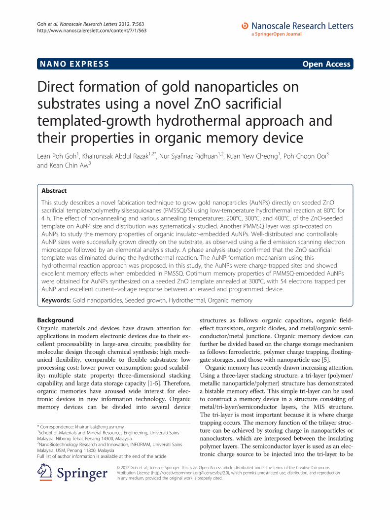
MethodsA n-type (100) silicon wafer was cut into small pieces(dimension of 1 × 1 cm) and used as substrates. The sili-con substrates were cleaned using a standard RCAcleaning process to remove the organic and inorganiccontaminants from the surface. A polymethylsilsequiox-ane (PMSSQ) layer was deposited at 2,000 rpm for 100 son the cleaned substrates to achieve 350-nm dielectriclayers. Thereafter, the samples were cured in an oven at160°C for 1 h (Figure 1a). A 200-nm-thick ZnO thin filmwas then deposited on each substrate using radio-frequency magnetron sputtering at 200 W (Figure 1b).The samples were annealed at different temperatures:200°C, 300°C, and 400°C, with a ramp rate and soakingtime of 5°C/min and 10 min, respectively, to observe theseed layer effects on AuNP formation (Figure 1c). There-after, the AuNPs were grown on the ZnO seed templateusing a sacrificial low-temperature hydrothermal ap-proach. The ZnO-seeded samples were subjected to ahydrothermal reaction in a preheated oven at 80°C for 4h. The hydrothermal bath contained 0.1 M zinc nitratetetrahydrate (Zn(NO3)2·4H2O), 0.1 M hexamethylenete-tramine (C6H12N4), 0.01 M gold(III) chloride trihydrate(AuCl4.3H2O), and 10 mL acetic acid. After hydrother-mal reaction, the samples were removed, rinsed withdeionized water, and then dried. The thin ZnO layer waseliminated due to sacrificial growth (Figure 1d).A second PMSSQ layer was then spin-coated on top
of AuNPs and cured at 160°C for 1 h (Figure 1e).Aluminum (Al) top (1 × 1 mm) and back contacts weredeposited using thermal evaporation (Figure 1f ).The surface morphology of the samples was observed
using a field emission scanning electron microscope(FESEM; Zeiss Supra™ 35VP, Carl Zeiss AG, Oberko-chen, Germany). The presence of chemical elements wasanalyzed using an energy dispersive X-ray spectrometer.Phase presence was analyzed using the Bruker D8 X-raydiffractometer (XRD; Bruker AXS GmbH, Karlsruhe,Germany). The memory characteristics of the sampleswere determined using the Keithley Model 4200-SCSsemiconductor characterization system (Keithley Instru-ments Inc., Cleveland, OH, USA).
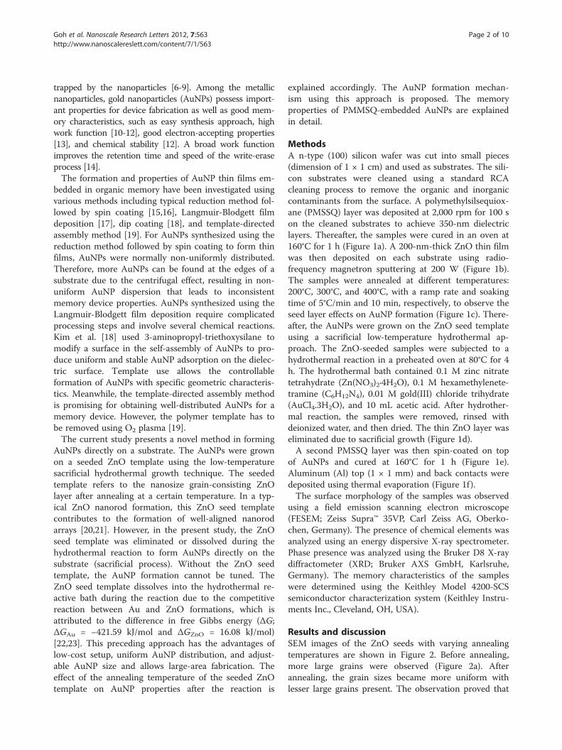
Results and discussionSEM images of the ZnO seeds with varying annealingtemperatures are shown in Figure 2. Before annealing,more large grains were observed (Figure 2a). Afterannealing, the grain sizes became more uniform withlesser large grains present. The observation proved that
Figure 1 Process flow for sacrificial templated-growth hydrothermal reaction of AuNPs embedded in the PMMSQ memory device. (a)PMMSQ/n-Si, (b) deposited ZnO layer, (c) thermal oxidation of ZnO layer to form ZnO seeds, (d) AuNPs formed on PMMSQ/n-Si, (e) anotherPMMSQ layer was deposited on the AuNPs, and (f) desired memory device structure with Al as top and bottom electrodes.
Goh et al. Nanoscale Research Letters 2012, 7:563 Page 3 of 10http://www.nanoscalereslett.com/content/7/1/563
the atoms rearranged to form a more stable microstruc-ture during the annealing process. The size of the grainsbecame smaller until annealing at 300°C (Figure 2c).Further increasing the annealing temperature to 400°Ccaused more large grain presence due to the diffusion ofions (Figure 2d). A similar result was reported by Chu
Figure 2 SEM images of the ZnO seed template annealed at varying
et al. [24]. However, for the hydrothermal growth usinga seeded template, the seeds must not be too dense toprovide a space for growth during the hydrothermalreaction.The average seed size of each sample was calculated
from SEM images using the ImageJ software (NIH,
temperatures. (a) Non-annealed, (b) 200°C, (c) 300°C, and (d) 400°C.

Goh et al. Nanoscale Research Letters 2012, 7:563 Page 4 of 10http://www.nanoscalereslett.com/content/7/1/563
Bethesda, MD, USA). The ZnO seed sizes of the non-annealed sample and those annealed at 200°C, 300°C,and 400°C were 110, 113, 109, and 104 nm, respectively.The ZnO seeds became smaller with increasing anneal-ing temperature. At high temperature, ZnO atoms vi-brate strongly at their lattice positions and exchangeenergy with neighboring atoms when sufficient thermalenergy is supplied during the annealing process. Thus,atoms diffuse to achieve the lowest strain energy [25],forming smaller ZnO seed surface grains (Figure 2).Figure 3a shows the XRD patterns of the ZnO seed
layer template annealed at different temperatures, witha preferential growth along (002) at 34.4° in all samples.The (002) peak intensities increased with increasingannealing temperature, indicating a crystallinity im-provement in the ZnO seeds. This crystallinity improve-ment is due to the sufficient thermal energy of theannealing process, which caused Zn and O atoms to re-arrange in a proper site. Thus, the ZnO seed layer tem-plate crystallinity is improved [26]. Moreover, the (002)peak positions shifted to a higher angle with increasedannealing temperature due to compressive stress relief.During the annealing process, the ZnO film atomsgained energy to rearrange; thus, the ZnO seed film
Figure 3 ZnO seed layer template, AuNP growth, and MIS memory deannealed at various temperatures. (b) Corresponding AuNP growth using t(c) Cross-sectional view of the MIS memory device for the sample annealed
achieved relaxation [24,27,28]. Meanwhile, ZnO peaksdisappear; however, a dominant peak of (111) at 38.3°Cappeared, which corresponds to the AuNP presence.Theoretically, for a face-centered cubic metal Au, thesurface energies of the low-index crystallographic facetsusually increase in the order of {111} < {100} < {110}due to an increase in interatomic distance. The {110}plane is the most favorable plane for the Au atom de-position because {110} has the highest facet surface en-ergy. Therefore, {110} planes have the highest rate ofdissolution and recrystallization of Au atoms, eventuallyresulting in {110} facet disappearance as the Au parti-cles grow, thereby making the synthesis of Au nanopar-ticle with {110} facets difficult. Therefore, Au prefers togrow along the {111} facets because the {111} facetshave the lowest surface energy, which is more stable, asshown in Figure 3b [29,30]. The ZnO peaks for all sam-ples were unobserved, confirming the dissolution of theZnO seed template during the hydrothermal reaction.This dissolution is attributed to the competitive growthbetween Au and ZnO. Furthermore, ZnO erodes in anacidic solution [31]. Therefore, in the present study, thepH of the hydrothermal precursor was similar for allsamples at approximately 2.7. Figure 3c shows the
vice. XRD spectra of the (a) sputtered ZnO seed layer templatehe ZnO seed template annealed at various temperatures.at 400°C.
Goh et al. Nanoscale Research Letters 2012, 7:563 Page 5 of 10http://www.nanoscalereslett.com/content/7/1/563
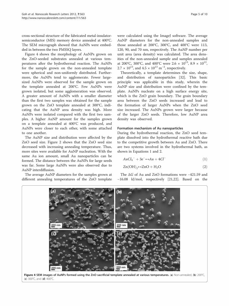
cross-sectional structure of the fabricated metal-insulator-semiconductor (MIS) memory device annealed at 400°C.The SEM micrograph showed that AuNPs were embed-ded in between the two PMSSQ layers.Figure 4 shows the morphology of AuNPs grown on
the ZnO-seeded substrates annealed at various tem-peratures after the hydrothermal reaction. The AuNPsfor the sample grown on the non-annealed templatewere spherical and non-uniformly distributed. Further-more, the AuNPs tend to agglomerate. Fewer large-sized AuNPs were observed for the sample grown onthe template annealed at 200°C. Few AuNPs weregrown isolated, but some agglomeration was observed.A greater amount of AuNPs with a smaller diameterthan the first two samples was obtained for the samplegrown on the ZnO template annealed at 300°C, indi-cating that the AuNP area density was high. MoreAuNPs were isolated compared with the first two sam-ples. A higher AuNP amount for the samples grownon a template annealed at 400°C was produced, andAuNPs were closer to each other, with some attachedto one another.The AuNP size and distribution were affected by the
ZnO seed size. Figure 2 shows that the ZnO seed sizedecreased with increasing annealing temperature. Thus,more sites were available for AuNP nucleation. With thesame Au ion amount, small Au nanoparticles can beformed. The distance between the AuNPs for large seedswas far. Some large AuNPs were also observed due toAuNP interdiffusion.The average AuNP diameters for the samples grown at
different annealing temperatures of the ZnO template
Figure 4 SEM images of AuNPs formed using the ZnO sacrificial temp(c) 300°C, and (d) 400°C.
were calculated using the ImageJ software. The averageAuNP diameters for the non-annealed samples andthose annealed at 200°C, 300°C, and 400°C were 113,120, 90, and 70 nm, respectively. The AuNP number perunit area (area density) was calculated. The area dens-ities of the non-annealed sample and samples annealedat 200°C, 300°C, and 400°C were 2.6 × 10¹³, 8.9 × 1012,2.7 × 1013, and 4.5 × 10¹³ m−2, respectively.Theoretically, a template determines the size, shape,
and distribution of nanoparticles [32]. This basicprinciple was applicable in this study, wherein theAuNP size and distribution were confined by the tem-plate. AuNPs nucleate on a high surface energy site,which is the ZnO grain boundary. The grain boundaryarea between the ZnO seeds increased and lead tothe formation of larger AuNPs when the ZnO seedsize increased. The AuNPs grown were larger becauseof the larger ZnO seeds. Therefore, low AuNP areadensity was observed.
Formation mechanism of Au nanoparticlesDuring the hydrothermal reaction, the ZnO seed tem-plate dissolved into the hydrothermal reactive bath dueto the competitive growth between Au and ZnO. Thereare two systems involved in the hydrothermal bath, asshown in Equations 1 and 2.
AuCl4� þ 3e�↔Auþ 4Cl� ð1Þ
Zn OHð Þ2↔ZnOþH2O ð2ÞThe ΔG of Au and ZnO formations were −421.59 and
−16.08 kJ/mol, respectively [21,22]. Based on the
late annealed at various temperatures. (a) Non-annealed, (b) 200°C,
Goh et al. Nanoscale Research Letters 2012, 7:563 Page 6 of 10http://www.nanoscalereslett.com/content/7/1/563
difference in ΔG values, AuNP formation was more fa-vorable; thus, ZnO formation was suppressed. Further-more, the precursor solution was acidic; ZnO erodes inan acidic condition [31]. ZnO is amphoteric and dis-solves in acids to form salts that contain hydrated zinc(II) cation [33]. Consequently, Zn(OH)2 dissociated backinto OH− and Zn2+ to neutralize the solution by reactingwith H+ ions in the precursor solution, as shown inEquations 3 and 4. Therefore, pH of the solution afterthe hydrothermal reaction increased.
Zn OHð Þ2↔Zn2þ þOH� ð3ÞHþ þ OH�↔H2O ð4Þ
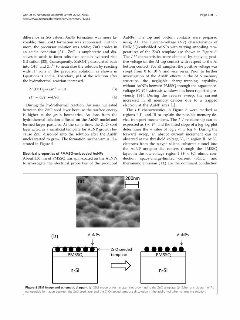
During the hydrothermal reaction, Au ions nucleatedbetween the ZnO seed layer because the surface energyis higher at the grain boundaries. Au ions from thehydrothermal solution diffused on the AuNP nuclei andformed larger particles. At the same time, the ZnO seedlayer acted as a sacrificial template for AuNP growth be-cause ZnO dissolved into the solution after the AuNPnuclei started to grow. The formation mechanism is illu-strated in Figure 5.
Electrical properties of PMMSQ-embedded AuNPsAbout 350 nm of PMSSQ was spin-coated on the AuNPsto investigate the electrical properties of the produced
Figure 5 SEM image and schematic diagram. (a) SEM image of Au nanonanoparticle formation between the ZnO seed layer and the ZnO-seeded t
AuNPs. The top and bottom contacts were preparedusing Al. The current–voltage (I-V) characteristics ofPMMSQ-embedded AuNPs with varying annealing tem-peratures of the ZnO template are shown in Figure 6.The I-V characteristics were obtained by applying posi-tive voltage on the Al top contact with respect to the Albottom contact. For all samples, the positive voltage wasswept from 0 to 10 V and vice versa. Prior to furtherinvestigation of the AuNP effects in the MIS memorystructure, the negligible charge-trapping capabilitywithout AuNPs between PMSSQ through the capacitance-voltage (C-V) hysteresis windows has been reported pre-viously [34]. During the reverse sweep, the currentincreased in all memory devices due to a trappedelectron at the AuNP sites [1].The I-V characteristics in Figure 6 were marked as
regions I, II, and III to explain the possible memory de-vice transport mechanisms. The I-V relationship can beexpressed as I∝ Vn, and the fitted slope of a log-log plotdetermines the n value of log I ∝ n log V. During theforward sweep, an abrupt current increment can beobserved at the threshold voltage,Vt,, in region II. At Vt,electrons from the n-type silicon substrate tunnel intothe AuNP acceptor-like centers through the PMSSQlayer. In the low-voltage region I (V < Vt), ohmic con-duction, space-charge-limited current (SCLC), andthermionic emission (TE) are the dominant conduction
particles grown using the ZnO template. (b) Schematic diagram of Auemplate dissolution in the acidic hydrothermal reactive solution.

Figure 6 I-V characteristics. (a) Non-annealed sample, (b) annealed at 200°C sample, (c) annealed at 300°C sample, and (d) annealed at 400°Csample as MIS memory devices.
Figure 7 Energy-band diagram. The diagram describes theelectron flows and trap observed during the positive bias on the Altop electrode with respect to the Al bottom contact.
Goh et al. Nanoscale Research Letters 2012, 7:563 Page 7 of 10http://www.nanoscalereslett.com/content/7/1/563
mechanisms, where electrons are being injected fromthe n-type Si into AuNPs. In ohmic conduction, n = 1.2and n = 0.9 for the memory devices that were non-annealed and annealed at 400°C, respectively. In SCLC,n = 2.8 for the memory device annealed at 200°C,whereas the log-log plot for the memory device annealedat 300°C does not fit the log I ∝ n log V relationshipbut fits the loge(J/T
2) ∝ V0.5, where J and T are thecurrent density and temperature of the system, indicat-ing that the TE mechanism was obeyed. As the voltageincreased to Vt, the transport mechanism switched tothe trapped charge-limited current for all memorydevices because n >>2 as marked in region II. In this re-gion, the trap sites due to the presence of AuNPs startedto be filled by electrons, and an abrupt current increasewas observed. After all traps in the AuNPs were filled,the transportation mechanism switched to trap-free (anideal SCLC transport mechanism has n = 2) SCLC forall cases. During the reverse sweep, the current flowthrough the device remained high because all the trapswere filled and followed the SCLC transport mechanism.The electrons can be stored and retained, thereby prov-ing the existence of the memory effect. An energy-banddiagram illustrates the electron injection from Si toPMSSQ and trapped in AuNPs, as described in Figure 7.The sample prepared using AuNPs grown on the non-
annealed template showed an abrupt increase at 6.8 V,which was the highest Vt observed among all samples,
with 0.8 orders of increment in current magnitude. Thispreceding aspect was due to the low area density of theAuNPs formed. For the sample grown on the templateannealed at 200°C, 0.7 orders of current magnitude in-crement was observed with lower Vt, 5.6 V. The lowAuNP area density was compensated by the larger andisolated AuNPs that stored more charges to obtain asimilar increment with the first sample, which was sup-ported by the findings on the effect of size on the

Goh et al. Nanoscale Research Letters 2012, 7:563 Page 8 of 10http://www.nanoscalereslett.com/content/7/1/563
memory window [35,36]. The largest hysteresis wasobtained for the sample prepared on the ZnO templateannealed at 300°C, with 6 orders of current magnitudeincrement at 3.6 V, indicating that uniform AuNPsobserved in combination with their size and area densityexhibited excellent memory effects. For the samplegrown on the template annealed at 400°C, 2 orders ofcurrent magnitude increment was observed at 2.4 V,which is attributed to the high area density of isolatedAuNPs. Based on the I-V characteristics, the samplesprepared using templates annealed at 300°C and 400°Cshowed larger current increment. Both samples showedgood distribution of isolated AuNPs when related backto the microstructure. The sample grown on the tem-plate annealed at 300°C produced better I-V responsesbetween an erased and programmed device. I-V plot isimportant as it allows the understanding of the chargetransport mechanism when the device is erased orprogrammed.The C-V characteristics of the PMMSQ-embedded
AuNPs using the ZnO template annealed at varying tem-peratures are shown in Figure 8. All samples were sweptfrom the negative to the positive voltage and then backto the negative voltage. The hysteresis (flat-band voltageshift, ΔVFB) window for the sample prepared on thenon-annealed template was 3.7 V, which was the largest
Figure 8 C-V characteristics of PMMSQ-embedded AuNPs. (a) Non-ann(d) 400°C.
hysteresis. The sample prepared on the templateannealed at 200°C exhibited the smallest hysteresis of1.2 V. Meanwhile, a large hysteresis of 3.6 V wasobserved in the sample grown on the template annealedat 300°C. No complete hysteresis window was observedfor the sample grown on the template annealed at 400°Cbecause the AuNPs formed were too dense and led tothe lateral flow of charges. Hence, the charge per Aunanoparticle was not calculated.The following illustrates the calculation of charge stor-
age capacity per AuNP. Flat-band voltage shift, ΔVFB,was calculated for a single electron (n = 1) confined inAuNPs using Equation 5:
ΔV FB ¼ nqdnanoparticleεPMSSQ
ðtgate þ 12DnanoparticleÞ ð5Þ
where n is the number of charges per single Au nano-particle, q is the electron charge magnitude, dnanoparticleis the area density, tgate is the thickness of the controlgate (PMSSQ), Dnanoparticle is the AuNP diameter, andεPMSSQ is the PMSSQ dielectric constant.Through the observed flat-band voltage shift, ΔVFBO,
from the C-V curve, the amount of charges stored persingle Au nanoparticle can be calculated as follows:
ealed samples and those (b) annealed at 200°C, (c) 300°C, and
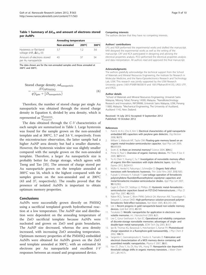
Table 1 Summary of ΔVFB and amount of electrons storedper AuNPs
Annealing temperature
Non-annealed 200°C 300°C
Hysteresis or flat-bandvoltage shift, ΔVFB (V)
3.7 1.2 3.6
Amount of electrons storedper Au nanoparticle
43 37 54
The data shown are for the non-annealed samples and those annealed at200°C and 300°C.
Goh et al. Nanoscale Research Letters 2012, 7:563 Page 9 of 10http://www.nanoscalereslett.com/content/7/1/563
Stored charge density; ndnanoparticle
¼ ΔVFBεPMSSQ
q tgate þ 12Dnanoparticle
� � ð6Þ
Therefore, the number of stored charge per single Aunanoparticle was obtained through the stored chargedensity in Equation 6, divided by area density, which is
represented as ndnanoparticlednanoparticle
.
The data obtained through the C-V characteristics ofeach sample are summarized in Table 1. Large hysteresiswas found for the sample grown on the non-annealedtemplate and at 300°C, 3.7 and 3.6 V, respectively. Fromthe microstructure observation, the latter sample had ahigher AuNP area density but had a smaller diameter.However, the hysteresis window size was slightly smallercompared with the sample grown on the non-annealedtemplate. Therefore, a larger Au nanoparticle size isprobably better for charge storage, which agrees withTseng and Tao [35]. The amount of charge stored perAu nanoparticle grown on the template annealed at300°C was 54, which is the highest compared with thesamples grown on the non-annealed and at 200°C(43 and 37, respectively). The results proved that thepresence of isolated AuNPs is important to obtainoptimum memory properties.
ConclusionsAuNPs were successfully grown directly on PMSSQusing a sacrificial templated growth hydrothermal reac-tion at a low temperature. The AuNP size and distribu-tion were dependent on the annealing temperature ofthe ZnO sacrificial template because AuNPs werenucleated and grown on ZnO seed grain boundaries.The AuNP size decreased, whereas the area densityincreased, with increasing ZnO annealing temperature.Optimum memory properties of the PMMSQ-embeddedAuNPs were obtained for AuNPs grown on the ZnOseed template annealed at 300°C, with an estimated 54electrons per Au nanoparticle and excellent I-Vresponses between an erased and programmed device.
Competing interestsThe authors declare that they have no competing interests.
Authors’ contributionsLPG and NSR performed the experimental works and drafted the manuscript.KAR designed the experimental works as well as the writing of themanuscript. CKY and KCA participated in designing and advising theelectrical properties analysis. PCO performed the electrical properties analysisand data interpretation. All authors read and approved the final manuscript.
AcknowledgmentsThe authors gratefully acknowledge the technical support from the Schoolof Materials and Mineral Resources Engineering, the Institute for Research inMolecular Medicine, and the Nano-Optoelectronics Research and TechnologyLab, USM. This research was jointly supported by the USM ResearchUniversity grants (1001/PSKBP/8630019 and 1001/PBahan/814135), LRGS UTP,and ERGS.
Author details1School of Materials and Mineral Resources Engineering, Universiti SainsMalaysia, Nibong Tebal, Penang 14300, Malaysia. 2NanoBiotechnologyResearch and Innovation, INFORMM, Universiti Sains Malaysia, USM, Penang11800, Malaysia. 3Mechanical Engineering, The University of Auckland,Auckland 1142, New Zealand.
Received: 14 July 2012 Accepted: 9 September 2012Published: 10 October 2012
References1. Park B, Im K-J, Cho K, Kim S: Electrical characteristics of gold nanoparticle-
embedded MIS capacitors with parylene gate dielectric. Org Electron2008, 9:878.
2. William S, Mabrook MF, Taylor DM: Floating-gate memory based on anorganic metal-insulator-semiconductor capacitor. Appl Phys Lett 2009,95:093309.
3. Scott JC: Is there an immortal memory? Science 2004, 304:62.4. Prime D, Paul S: Overview of organic memory devices. Phil Trans R Soc A
2009, 367:4141.5. Yu H, Chen Y, Huang C, Su Y: Investigation of nonvolatile memory effect
of organic thin-film transistors with triple dielectric layers. Appl PhysExpress 2012, 5:034101.
6. Müller K, Henkel K, Paloumpa I, Schmeiβer D: Organic field effecttransistors with ferroelectric hysteresis. Thin Solid Films 2007, 515:7683.
7. Fujisaki S, Ishiwara H, Fukisaki Y: Low-voltage operation of ferroelectricpoly(vinylidene fluoridetrifluoroethylene) copolymer capacitors andmetal-ferroelectric-insulator-semiconductor diodes. Appl Phys Lett 2007,90:162902.
8. Cagin E, Chen DY, Siddiqui JJ, Phillips JD: Hysteretic metal–ferroelectric–semiconductor capacitors based on PZT/ZnO heterostructures. J Phys D:Appl Phys 2007, 40:2430.
9. Naber RCG, Tanase C, Blom PWM, Gelinck GH, Marsman AW, Touwslager FJ,Setayesh S, Leeuw DMD: High-performance solution-processed polymerferroelectric field-effect transistors. Nat Mater 2005, 4(3):243–248.
10. Lee J: Recent progress in gold nanoparticle-based non-volatile memorydevices. Gold Bull 2010, 43:189.
11. Tsoukalas D: Metallic nanoparticles for application in electronic non-volatile memories. Int J Nanotechnol 2009, 6:35.
12. Lee C, Gorur-Seetharam A, Kan EC: Operational and reliability comparisonof discrete-storage nonvolatile memories: advantages of single- anddouble-layer metal nanocrystals. IEDM Tech Dig 2003, 3:557.
13. Ipe BI, Thomas KG, Barazzouk S, Hotchandani S, Kamat PV: Photoinducedcharge separation in a fluorophore-gold nanoassembly. J Phys Chem B2002, 106:18.
14. Sargentis C, Giannakopoulos K, Travlos A, Tsamakis D: Fabrication andelectrical characterization of a MOS memory device containing self-assembled metallic nanoparticles. Physica E 2007, 38:85.
15. Han ST, Zhou Y, Xu ZX, Roy VAL, Hung TF: Nanoparticle size dependentthreshold voltage shifts in organic memory transistors. J Mater Chem2011, 21:14575.

Goh et al. Nanoscale Research Letters 2012, 7:563 Page 10 of 10http://www.nanoscalereslett.com/content/7/1/563
16. Prakash A, Ouyang J, Lin J, Yang Y: Polymer memory device based onconjugated polymer and gold nanoparticles. J Appl Phys 2006,100:054309.
17. Paul S, Pearson C, Molloy A, Cousins MA, Green M, Kolliopoulou S, DimitrakisP, Normand P, Tsoukalas D, Petty MC: Langmuir-Blodgett film depositionof metallic nanoparticles and their application to electronic memorystructures. Nano Lett 2003, 3:533.
18. Kim H, Jung S, Kim B, Yoon T, Kim Y, Lee H: Characterization of chargingeffect of citrate-capped Au nanoparticle pentacene device. J Ind EngChem 2010, 16:848.
19. Gupta RK, Krishnamoorthy S, Kusuma DY, Lee PS, Srinivasan MP: Enhancingcharge-storage capacity of non-volatile memory devices using template-directed assembly of gold nanoparticles. Nanoscale 2012, 4:2296.
20. Tan WK, Razak KA, Ibrahim K, Lockman Z: Formation of ZnO nanorodarrays on polytetraflouroethylene (PTFE) via a seeded growth lowtemperature hydrothermal reaction. J Alloys Compd 2011, 509:820.
21. Lockman Z, Pet Fong Y, Wai Kian T, Ibrahim K, Razak KA: Formation of self-aligned ZnO nanorods in aqueous solution. J Alloys Compd 2010, 493:699.
22. Davies A, Staveley LAK: The thermodynamics of the stable modification ofzinc hydroxide, and the standard entropy of the aqueous zinc ion.J Chem Thermodyn 1972, 4:267.
23. Marsden JO, Lain CI: The Chemistry of Gold Extraction. Colorado: Society forMining, Metallurgy and Exploration Inc; 2006.
24. Chu SY, Water W, Liaw JT: Influence of postdeposition annealing on theproperties of ZnO films prepared by RF magnetron sputtering. J EurCeram Soc 2003, 23:1593.
25. Mittemeijer EJ: Fundamentals of Materials Science: The Microstructure-PropertyRelationship Using Metals as Model Systems. New York: Springer; 2011.
26. Liu SY, Chen T, Wan J, Ru GP, Li BZ, Qu XP: The effect of pre-annealing ofsputtered ZnO seed layers on growth of ZnO nanorods through ahydrothermal method. Appl Phys A 2009, 94:775.
27. Karamdel J, Dee CF, Majlis BY: Effects of annealing conditions on thesurface morphology and crystallinity of sputtered ZnO nano films. SainsMalaysiana 2011, 40:209.
28. Sun X, Fu Z, Wu Z: Fractal processing of AFM images of rough ZnO films.Mater Charact 2002, 48:169.
29. Personick ML, Langille MR, Zhang J, Harris N, Schatz GC, Mirkin CA:Synthesis and isolation of {110}-faceted gold bipyramids and rhombicdodecahedra. J Am Chem Soc 2011, 133:6170.
30. Bakshi MS, Sachar S, Kaur G, Bhandari P, Biesinger MC, Possmayer F,Petersen NO: Dependence of crystal growth of gold nanoparticles on thecapping behavior of surfactant at ambient conditions. Cryst Growth Des2008, 8:1713.
31. Baruah S, Dutta J: pH-dependent growth of zinc oxide nanorods. J CrystGrowth 2009, 311:2549.
32. Hulteen JC, Martin CR: A general template-based method for thepreparation of nanomaterials. J Mater Chem 1997, 7:1075.
33. Degen A, Kosec M: Effect of pH and impurities on the surface charge ofzinc oxide in aqueous solution. J Eur Ceram Soc 2000, 20:667.
34. Ahmad Z, Ooi PC, Aw KC, Sayyad MH: Electrical characteristics of poly(methylsilsesquioxane) thin films for non-volatile memory. Solid StateCommun 2011, 151:297.
35. Tseng C, Tao Y: Electric bistability in pentacene film-based transistorembedding gold nanoparticles. J Am Chem Soc 2009, 131:12441.
36. Houili H, Tutis E, Izquierdo R: Modeling nanoparticle embedded organicmemory devices. Org Electron 2010, 11:514.
doi:10.1186/1556-276X-7-563Cite this article as: Goh et al.: Direct formation of gold nanoparticles onsubstrates using a novel ZnO sacrificial templated-growth hydrothermalapproach and their properties in organic memory device. NanoscaleResearch Letters 2012 7:563.
Submit your manuscript to a journal and benefi t from:
7 Convenient online submission
7 Rigorous peer review
7 Immediate publication on acceptance
7 Open access: articles freely available online
7 High visibility within the fi eld
7 Retaining the copyright to your article
Submit your next manuscript at 7 springeropen.com