mx25l512 datasheet - natisbad.orgnatisbad.org/nas5/refs/mx25l512_3v_512kb_v1.7.pdf · mx25l512...
TRANSCRIPT
REV. 1.7, APR. 15, 20091
P/N: PM1214
MX25L512
MX25L512 DATASHEET
The MX25L512 product family is not recommended for new designs. The MX25L512C family is the recommended replacement. Please refer to MX25L512C datasheet for full specifications and ordering information, or contact your local sales representative for additional support.

2P/N: PM1214 REV. 1.7, APR. 15, 2009
MX25L512
FEATURES
GENERAL• Serial Peripheral Interface (SPI) compatible -- Mode 0 and Mode 3• 524,288 x 1 bit structure • 16 Equal Sectors with 4K byte each - Any Sector can be erased individually• Single Power Supply Operation - 2.7 to 3.6 volt for read, erase, and program operations• Latch-up protected to 100mA from -1V to Vcc +1V
PERFORMANCE• High Performance - Fast access time: 85MHz serial clock (15pF + 1TTL Load) and 66MHz serial clock (30pF + 1TTL Load) - Fast program time: 1.4ms(typ.) and 5ms(max.)/page (256-byte per page) - Fast erase time: 60ms(typ.) and 120ms(max.)/sector (4K-byte per sector) ; 1s(typ.) and 2s(max.)/chip(512Kb)• Low Power Consumption - Low active read current: 12mA(max.) at 85MHz, 8mA(max.) at 66MHz and 4mA(max.) at 33MHz - Low active programming current: 15mA (max.) - Low active erase current: 15mA (max.) - Low standby current: 10uA (max.)
- Deep power-down mode 1uA (typical)• Minimum 100,000 erase/program cycles
SOFTWARE FEATURES• Input Data Format - 1-byte Command code• Block Lock protection - The BP0~BP1 status bit defines the size of the area to be software protected against Program and Erase in-
structions.• Auto Erase and Auto Program Algorithm
- Automatically erases and verifies data at selected sector - Automatically programs and verifies data at selected page by an internal algorithm that automatically times the
program pulse widths (Any page to be programed should have page in the erased state first)
512K-BIT [x 1] CMOS SERIAL FLASH
The MX25L512 product family is not recommended for new designs. The MX25L512C family is the recommended replacement. Please refer to MX25L512C datasheet for full specifications and ordering information, or contact your local sales representative for additional support.
3P/N: PM1214 REV. 1.7, APR. 15, 2009
MX25L512
• Status Register Feature• Electronic Identification
- JEDEC 2-byte Device ID - RES command, 1-byte Device ID
HARDWARE FEATURES• SCLK Input
- Serial clock input• SI Input
- Serial Data Input• SO Output
- Serial Data Output• WP# pin
- Hardware write protection• HOLD# pin
- pause the chip without diselecting the chip • PACKAGE - 8-pin SOP (150mil) - 8-USON (2x3mm) - All Pb-free devices are RoHS Compliant
GENERAL DESCRIPTION
MX25L512 is a CMOS 524,288 bit serial Flash memory, which is configured as 65,536 x 8 internally. MX25L512 features a serial peripheral interface and software protocol allowing operation on a simple 3-wire bus. The three bus signals are a clock input (SCLK), a serial data input (SI), and a serial data output (SO). SPI access to the device is enabled by CS# input.
MX25L512 provide sequential read operation on whole chip.
After program/erase command is issued, auto program/ erase algorithms which program/ erase and verify the spec-ified page or sector/block locations will be executed. Program command is executed on page (256 bytes) basis, and erase command is executes on chip or sector (4K-bytes).
To provide user with ease of interface, a status register is included to indicate the status of the chip. The status read command can be issued to detect completion status of a program or erase operation via WIP bit.
When the device is not in operation and CS# is high, it is put in standby mode and draws less than 10uA DC cur-rent.
The MX25L512 utilize MXIC's proprietary memory cell, which reliably stores memory contents even after 100,000 program and erase cycles.

4P/N: PM1214 REV. 1.7, APR. 15, 2009
MX25L512
PIN CONFIGURATIONS
SYMBOL DESCRIPTIONCS# Chip SelectSI Serial Data InputSO Serial Data Output
SCLK Clock InputHOLD# Hold, to pause the device without
deselecting the deviceWP# Write ProtectionVCC + 3.3V Power SupplyGND Ground
PIN DESCRIPTION
8-PIN SOP (150mil)
1234
CS#SO
WP#GND
VCCHOLD#SCLKSI
8765
8-LAND USON (2x3mm)
1234
CS#SO
WP#GND
8765
VCCHOLD#SCLKSI

5P/N: PM1214 REV. 1.7, APR. 15, 2009
MX25L512
BLOCK DIAGRAM
AddressGenerator
Memory Array
Page Buffer
Y-Decoder
X-D
ecoder
DataRegister
SRAMBuffer
SI
SCLK Clock Generator
StateMachine
ModeLogic
SenseAmplifier
HVGenerator
OutputBuffer
SO
CS#

6P/N: PM1214 REV. 1.7, APR. 15, 2009
MX25L512
DATA PROTECTION
MX25L512 is designed to offer protection against accidental erasure or programming caused by spurious system level signals that may exist during power transition. During power up the device automatically resets the state ma-chine in the standby mode. In addition, with its control register architecture, alteration of the memory contents only occurs after successful completion of specific command sequences. The device also incorporates several features to prevent inadvertent write cycles resulting from VCC power-up and power-down transition or system noise.
• Valid command length checking: The command length will be checked whether it is at byte base and completed on byte boundary.
• Write Enable (WREN) command: WREN command is required to set the Write Enable Latch bit (WEL) before other command to change data. The WEL bit will return to reset stage under following situation:
- Power-up - Write Disable (WRDI) command completion - Write Status Register (WRSR) command completion - Page Program (PP) command completion - Sector Erase (SE) command completion - Block Erase (BE) command completion - Chip Erase (CE) command completion
• Software Protection Mode (SPM): by using BP0-BP1 bits to set the part of Flash protected from data change.
• Hardware Protection Mode (HPM): by using WP# going low to protect the BP0-BP1 bits and SRWD bit from data change.
• Deep Power Down Mode: By entering deep power down mode, the flash device also is under protected from writing all commands except Release from deep power down mode command (RDP) and Read Electronic Sig-nature command (RES).
7P/N: PM1214 REV. 1.7, APR. 15, 2009
MX25L512
Table 1. Protected Area SizesStatus bit Protect level 512bBP1 BP0
0 0 0 (none) None 0 1 1 (All) All1 0 2 (All) All1 1 3 (All) All
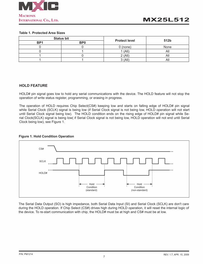
HOLD FEATURE
HOLD# pin signal goes low to hold any serial communications with the device. The HOLD feature will not stop the operation of write status register, programming, or erasing in progress.
The operation of HOLD requires Chip Select(CS#) keeping low and starts on falling edge of HOLD# pin signal while Serial Clock (SCLK) signal is being low (if Serial Clock signal is not being low, HOLD operation will not start until Serial Clock signal being low). The HOLD condition ends on the rising edge of HOLD# pin signal while Se-rial Clock(SCLK) signal is being low( if Serial Clock signal is not being low, HOLD operation will not end until Serial Clock being low), see Figure 1.
The Serial Data Output (SO) is high impedance, both Serial Data Input (SI) and Serial Clock (SCLK) are don't care during the HOLD operation. If Chip Select (CS#) drives high during HOLD operation, it will reset the internal logic of the device. To re-start communication with chip, the HOLD# must be at high and CS# must be at low.
HOLD#
CS#
SCLK
HoldCondition
(standard)
HoldCondition
(non-standard)
Figure 1. Hold Condition Operation

8P/N: PM1214 REV. 1.7, APR. 15, 2009
MX25L512
Table 2. COMMAND DEFINITION
(1) ADD=00H will output the manufacturer's ID first and ADD=01H will output device ID first.(2) BE command may erase whole 512Kb chip.(3) It is not recommended to adopt any other code which is not in the above command definition table.
COMMAND (byte)
WREN (write enable)
WRDI (write disable)
RDID (read identification)
RDSR (read status
register)
WRSR (write status
register)
READ(read data)
Fast Read(fast read
data)1st 06 (hex) 04 (hex) 9F (hex) 05 (hex) 01 (hex) 03 (hex) 0B (hex)2nd AD1 AD13rd AD2 AD24th AD3 AD35th x
Action
sets the (WEL) write enable
latch bit
resets the (WEL) write enable latch
bit
outputs manufacturer ID and 2-byte
device ID
to read out the status register
to write new values to the status register
n bytes read out until CS#
goes high
COMMAND (byte)
SE(Sector Erase)
BE (2)(Block Erase)
CE (Chip Erase)
PP(Page Program)
DP(Deep Power Down)
RDP (Release
from Deep Power-down)
RES (Read Electronic
ID)
REMS (Read Electronic
Manufacturer & Device ID)
1st 20 (hex) 52 or D8 (hex)
60 or C7 (hex) 02 (hex) B9 (hex) AB (hex) AB (hex) 90 (hex)
2nd AD1 AD1 AD1 x x3rd AD2 AD2 AD2 x x4th AD3 AD3 AD3 x ADD(1)5th
Action
Output the manufacturer ID and device
ID
9P/N: PM1214 REV. 1.7, APR. 15, 2009
MX25L512
DEVICE OPERATION
1. Before a command is issued, status register should be checked to ensure device is ready for the intended op-eration.
2. When incorrect command is inputted to this LSI, this LSI becomes standby mode and keeps the standby mode until next CS# falling edge. In standby mode, SO pin of this LSI should be High-Z.
3. When correct command is inputted to this LSI, this LSI becomes active mode and keeps the active mode until next CS# rising edge.
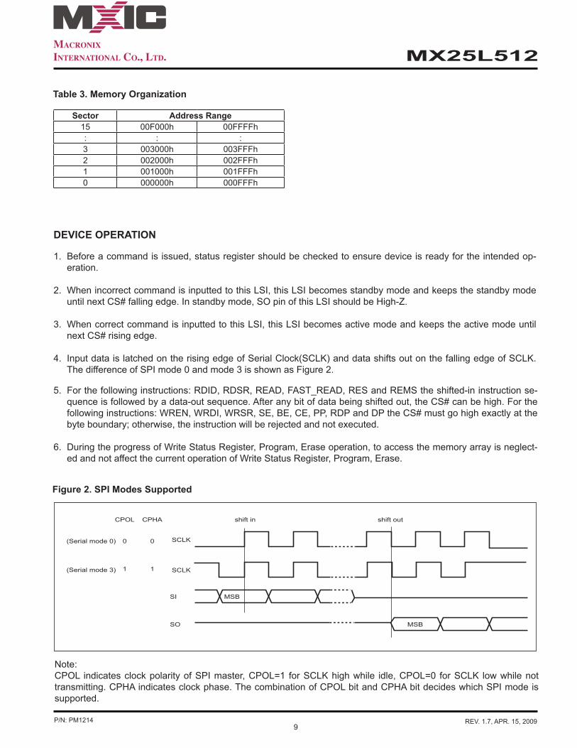
4. Input data is latched on the rising edge of Serial Clock(SCLK) and data shifts out on the falling edge of SCLK. The difference of SPI mode 0 and mode 3 is shown as Figure 2.
Figure 2. SPI Modes Supported
SCLK
MSB
CPHA shift in shift out
SI
0
1
CPOL
0(Serial mode 0)
(Serial mode 3) 1
SO
SCLK
MSB
5. For the following instructions: RDID, RDSR, READ, FAST_READ, RES and REMS the shifted-in instruction se-quence is followed by a data-out sequence. After any bit of data being shifted out, the CS# can be high. For the following instructions: WREN, WRDI, WRSR, SE, BE, CE, PP, RDP and DP the CS# must go high exactly at the byte boundary; otherwise, the instruction will be rejected and not executed.
6. During the progress of Write Status Register, Program, Erase operation, to access the memory array is neglect-ed and not affect the current operation of Write Status Register, Program, Erase.
Table 3. Memory Organization
Note:CPOL indicates clock polarity of SPI master, CPOL=1 for SCLK high while idle, CPOL=0 for SCLK low while not transmitting. CPHA indicates clock phase. The combination of CPOL bit and CPHA bit decides which SPI mode is supported.
Sector Address Range15 00F000h 00FFFFh: : :3 003000h 003FFFh2 002000h 002FFFh1 001000h 001FFFh0 000000h 000FFFh
10P/N: PM1214 REV. 1.7, APR. 15, 2009
MX25L512
COMMAND DESCRIPTION
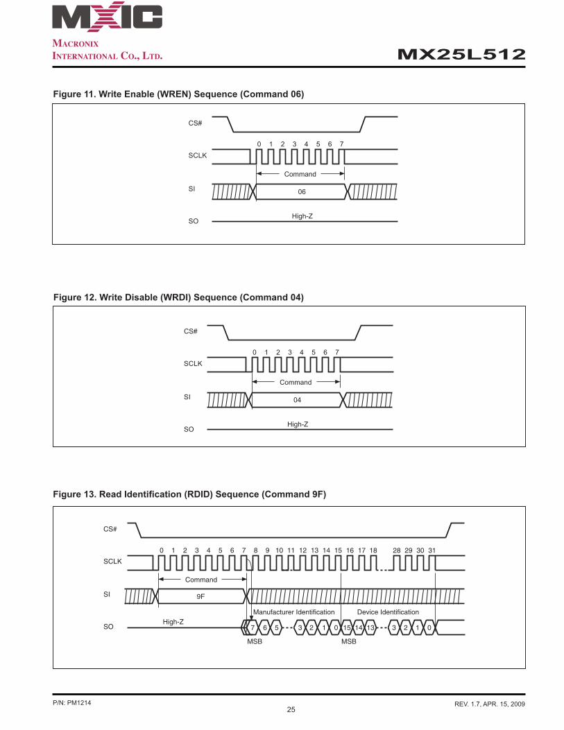
(1) Write Enable (WREN)
The Write Enable (WREN) instruction is for setting Write Enable Latch (WEL) bit. For those instructions like PP, SE, BE, CE, and WRSR, which are intended to change the device content, should be set every time after the WREN in-struction setting the WEL bit.
The sequence of issuing WREN instruction is: CS# goes low-> sending WREN instruction code-> CS# goes high. (see Figure 11)
(2) Write Disable (WRDI)
The Write Disable (WRDI) instruction is for resetting Write Enable Latch (WEL) bit.
The sequence of issuing WRDI instruction is: CS# goes low-> sending WRDI instruction code-> CS# goes high. (see Figure 12)
The WEL bit is reset by following situations: - Power-up - Write Disable (WRDI) instruction completion - Write Status Register (WRSR) instruction completion - Page Program (PP) instruction completion - Sector Erase (SE) instruction completion - Block Erase (BE) instruction completion - Chip Erase (CE) instruction completion
(3) Read Identification (RDID)
RDID instruction is for reading the manufacturer ID of 1-byte and followed by Device ID of 2-byte. The MXIC Manu-facturer ID is C2(hex), the memory type ID is 20(hex) as the first-byte device ID, and the individual device ID of second-byte ID is as followings: 10(hex) for MX25L512.
The sequence of issuing RDID instruction is: CS# goes low→sending RDID instruction code→24-bits ID data out on SO→to end RDID operation can use CS# to high at any time during data out. (see Figure. 13)
While Program/Erase operation is in progress, it will not decode the RDID instruction, so there's no effect on the cy-cle of program/erase operation which is currently in progress. When CS# goes high, the device is at standby stage.
11P/N: PM1214 REV. 1.7, APR. 15, 2009
MX25L512
(4) Read Status Register (RDSR)
The RDSR instruction is for reading Status Register Bits. The Read Status Register can be read at any time (even in program/erase/write status register condition) and continuously. It is recommended to check the Write in Progress (WIP) bit before sending a new instruction when a program, erase, or write status register operation is in progress.
The sequence of issuing RDSR instruction is: CS# goes low→sending RDSR instruction code→Status Register data out on SO (see Figure. 14)
The definition of the status register bits is as below:
WIP bit. The Write in Progress (WIP) bit, a volatile bit, indicates whether the device is busy in program/erase/write status register progress. When WIP bit sets to 1, which means the device is busy in program/erase/write status register progress. When WIP bit sets to 0, which means the device is not in progress of program/erase/write status register cycle.
WEL bit. The Write Enable Latch (WEL) bit, a volatile bit, indicates whether the device is set to internal write enable latch. When WEL bit sets to 1, which means the internal write enable latch is set, the device can accept program/erase/write status register instruction. When WEL bit sets to 0, which means no internal write enable latch; the de-vice will not accept program/erase/write status register instruction.
BP1, BP0 bits. The Block Protect (BP1, BP0) bits, non-volatile bits, indicate the protected area(as defined in table 1) of the device to against the program/erase instruction without hardware protection mode being set. To write the Block Protect (BP1, BP0) bits requires the Write Status Register (WRSR) instruction to be executed. Those bits define the protected area of the memory to against Page Program (PP), Sector Erase (SE), Block Erase (BE) and Chip Erase(CE) instructions (only if all Block Protect bits set to 0, the CE instruction can be executed)
SRWD bit. The Status Register Write Disable (SRWD) bit, non-volatile bit, is operated together with Write Protec-tion (WP#) pin for providing hardware protection mode. The hardware protection mode requires SRWD sets to 1 and WP# pin signal is low stage. In the hardware protection mode, the Write Status Register (WRSR) instruction is no longer accepted for execution and the SRWD bit and Block Protect bits (BP1, BP0) are read only.
Note: 1. See the table "Protected Area Sizes". 2. The endurance cycles of protect bits are 100,000 cycles; however, the tW time out spec of protect bits is
relaxed as tW = N x 15ms (N is a multiple of 10,000 cycles, ex. N = 2 for 20,000 cycles) after 10,000 cycles on those bits.
bit7 bit6 bit5 bit4 bit3 bit2 bit1 bit0
SRWD (status register write
protect)0 0 0
BP1 (level of
protected block)
BP0 (level of
protected block)
WEL(write enable
latch)
WIP(write in
progress bit)
1=status register write
disable(note 1) (note 1)
1=write enable
0=not write enable
1=write operation
0=not in write operation
12P/N: PM1214 REV. 1.7, APR. 15, 2009
MX25L512
(5) Write Status Register (WRSR)
The WRSR instruction is for changing the values of Status Register Bits. Before sending WRSR instruction, the Write Enable (WREN) instruction must be decoded and executed to set the Write Enable Latch (WEL) bit in ad-vance. The WRSR instruction can change the value of Block Protect (BP1, BP0) bits to define the protected area of memory (as shown in table 1). The WRSR also can set or reset the Status Register Write Disable (SRWD) bit in accordance with Write Protection (WP#) pin signal. The WRSR instruction cannot be executed once the Hardware Protected Mode (HPM) is entered.
The sequence of issuing WRSR instruction is: CS# goes low-> sending WRSR instruction code-> Status Register data on SI-> CS# goes high. (see Figure 15)
The WRSR instruction has no effect on b6, b5, b4, b1, b0 of the status register.
The CS# must go high exactly at the byte boundary; otherwise, the instruction will be rejected and not executed. The self-timed Write Status Register cycle time (tW) is initiated as soon as Chip Select (CS#) goes high. The Write in Progress (WIP) bit still can be check out during the Write Status Register cycle is in progress. The WIP sets 1 during the tW timing, and sets 0 when Write Status Register Cycle is completed, and the Write Enable Latch (WEL) bit is reset.
Table 4. Protection Modes
Note: 1. As defined by the values in the Block Protect (BP1, BP0) bits of the Status Register, as shown in Table 1.
As the table above showing, the summary of the Software Protected Mode (SPM) and Hardware Protected Mode (HPM).
Software Protected Mode (SPM): - When SRWD bit=0, no matter WP# is low or high, the WREN instruction may set the WEL bit and can change
the values of SRWD, BP1, BP0. The protected area, which is defined by BP1, BP0, is at software protected mode (SPM).
- When SRWD bit=1 and WP# is high, the WREN instruction may set the WEL bit can change the values of SRWD, BP1, BP0. The protected area, which is defined by BP1, BP0, is at software protected mode (SPM)
Mode Status register condition WP# and SRWD bit status Memory
Software protectionmode (SPM)
Status register can be writtenin (WEL bit is set to "1") and
the SRWD, BP0-BP1bits can be changed
WP#=1 and SRWD bit=0, orWP#=0 and SRWD bit=0, or
WP#=1 and SRWD=1
The protected area cannot
be program or erase.
Hardware protectionmode (HPM)
The SRWD, BP0-BP1 ofstatus register bits cannot be
changedWP#=0, SRWD bit=1
The protected area cannot
be program or erase.
13P/N: PM1214 REV. 1.7, APR. 15, 2009
MX25L512
Note: If SRWD bit=1 but WP# is low, it is impossible to write the Status Register even if the WEL bit has previously been set. It is rejected to write the Status Register and not be executed.
Hardware Protected Mode (HPM):- When SRWD bit=1, and then WP# is low (or WP# is low before SRWD bit=1), it enters the hardware protected
mode (HPM). The data of the protected area is protected by software protected mode by BP1, BP0 and hard-ware protected mode by the WP# to against data modification.
Note: to exit the hardware protected mode requires WP# driving high once the hardware protected mode is entered. If the WP# pin is permanently connected to high, the hardware protected mode can never be entered; only can use software protected mode via BP1, BP0.
(6) Read Data Bytes (READ)
The read instruction is for reading data out. The address is latched on rising edge of SCLK, and data shifts out on the falling edge of SCLK at a maximum frequency fR. The first address byte can be at any location. The address is automatically increased to the next higher address after each byte data is shifted out, so the whole memory can be read out at a single READ instruction. The address counter rolls over to 0 when the highest address has been reached.
The sequence of issuing READ instruction is: CS# goes low→ sending READ instruction code→ 3-byte address on SI→ data out on SO→ to end READ operation can use CS# to high at any time during data out. (see Figure. 16)
(7) Read Data Bytes at Higher Speed (FAST_READ)
The FAST_READ instruction is for quickly reading data out. The address is latched on rising edge of SCLK, and data of each bit shifts out on the falling edge of SCLK at a maximum frequency fC. The first address byte can be at any location. The address is automatically increased to the next higher address after each byte data is shifted out, so the whole memory can be read out at a single FAST_READ instruction. The address counter rolls over to 0 when the highest address has been reached.
The sequence of issuing FAST_READ instruction is: CS# goes low→ sending FAST_READ instruction code→ 3-byte address on SI→ 1-dummy byte address on SI→data out on SO→ to end FAST_READ operation can use CS# to high at any time during data out. (see Figure. 17)
While Program/Erase/Write Status Register cycle is in progress, FAST_READ instruction is rejected without any im-pact on the Program/Erase/Write Status Register current cycle.
(8) Sector Erase (SE)
The Sector Erase (SE) instruction is for erasing the data of the chosen sector to be "1". A Write Enable (WREN) in-struction must execute to set the Write Enable Latch (WEL) bit before sending the Sector Erase (SE). Any address of the sector (see table 3) is a valid address for Sector Erase (SE) instruction. The CS# must go high exactly at the byte boundary (the latest eighth of address byte been latched-in); otherwise, the instruction will be rejected and not executed.
Address bits [Am-A12] (Am is the most significant address) select the sector address.
The sequence of issuing SE instruction is: CS# goes low → sending SE instruction code→ 3-byte address on SI → CS# goes high. (see Figure 19)

14P/N: PM1214 REV. 1.7, APR. 15, 2009
MX25L512
The self-timed Sector Erase Cycle time (tSE) is initiated as soon as Chip Select (CS#) goes high. The Write in Progress (WIP) bit still can be check out during the Sector Erase cycle is in progress. The WIP sets 1 during the tSE timing, and sets 0 when Sector Erase Cycle is completed, and the Write Enable Latch (WEL) bit is reset. If the page is protected by BP1, BP0 bits, the Sector Erase (SE) instruction will not be executed on the page.
(9) Block Erase (BE)
The Block Erase (BE) instruction is for erasing the data of the chosen block to be "1". A Write Enable (WREN) in-struction must execute to set the Write Enable Latch (WEL) bit before sending the Block Erase (BE). Any address of the block (see table 3) is a valid address for Block Erase (BE) instruction. The CS# must go high exactly at the byte boundary (the latest eighth of address byte been latched-in); otherwise, the instruction will be rejected and not executed.
The sequence of issuing BE instruction is: CS# goes low → sending BE instruction code→ 3-byte address on SI → CS# goes high. (see Figure 20)
The self-timed Block Erase Cycle time (tBE) is initiated as soon as Chip Select (CS#) goes high. The Write in Progress (WIP) bit still can be check out during the Sector Erase cycle is in progress. The WIP sets 1 during the tBE timing, and sets 0 when Sector Erase Cycle is completed, and the Write Enable Latch (WEL) bit is reset. If the page is protected by BP1, BP0 bits, the Block Erase (BE) instruction will not be executed on the page.
(10) Chip Erase (CE)
The Chip Erase (CE) instruction is for erasing the data of the whole chip to be "1". A Write Enable (WREN) instruc-tion must execute to set the Write Enable Latch (WEL) bit before sending the Chip Erase (CE). Any address of the sector (see table 3) is a valid address for Chip Erase (CE) instruction. The CS# must go high exactly at the byte boundary( the latest eighth of address byte been latched-in); otherwise, the instruction will be rejected and not ex-ecuted.
The sequence of issuing CE instruction is: CS# goes low→ sending CE instruction code→ CS# goes high. (see Figure 20)
The self-timed Chip Erase Cycle time (tCE) is initiated as soon as Chip Select (CS#) goes high. The Write in Progress (WIP) bit still can be check out during the Chip Erase cycle is in progress. The WIP sets 1 during the tCE timing, and sets 0 when Chip Erase Cycle is completed, and the Write Enable Latch (WEL) bit is reset. If the chip is protected by BP1, BP0 bits, the Chip Erase (CE) instruction will not be executed. It will be only executed when BP1, BP0 all set to "0".
(11) Page Program (PP)
The Page Program (PP) instruction is for programming the memory to be "0". A Write Enable (WREN) instruction must execute to set the Write Enable Latch (WEL) bit before sending the Page Program (PP). If the eight least sig-nificant address bits (A7-A0) are not all 0, all transmitted data which goes beyond the end of the current page are programmed from the start address if the same page (from the address whose 8 least significant address bits (A7-A0) are all 0). The CS# must keep during the whole Page Program cycle. The CS# must go high exactly at the byte boundary( the latest eighth of address byte been latched-in); otherwise, the instruction will be rejected and not executed. If more than 256 bytes are sent to the device, the data of the last 256-byte is programmed at the request page and previous data will be disregarded. If less than 256 bytes are sent to the device, the data is programmed at the request address of the page without effect on other address of the same page.
The sequence of issuing PP instruction is: CS# goes low→ sending PP instruction code→ 3-byte address on SI→

15P/N: PM1214 REV. 1.7, APR. 15, 2009
MX25L512
(12) Deep Power-down (DP)
The Deep Power-down (DP) instruction is for setting the device on the minimizing the power consumption (to enter-ing the Deep Power-down mode), the standby current is reduced from ISB1 to ISB2). The Deep Power-down mode requires the Deep Power-down (DP) instruction to enter, during the Deep Power-down mode, the device is not ac-tive and all Write/Program/Erase instruction are ignored. When CS# goes high, it's only in standby mode not deep power-down mode. It's different from Standby mode.
The sequence of issuing DP instruction is: CS# goes low→ sending DP instruction code→ CS# goes high. (see Fig-ure 22)
Once the DP instruction is set, all instruction will be ignored except the Release from Deep Power-down mode (RDP) and Read Electronic Signature (RES) instruction. (RES instruction to allow the ID been read out). When Power-down, the deep power-down mode automatically stops, and when power-up, the device automatically is in standby mode. For RDP instruction the CS# must go high exactly at the byte boundary (the latest eighth bit of instruction code been latched-in); otherwise, the instruction will not executed. As soon as Chip Select (CS#) goes high, a delay of tDP is required before entering the Deep Power-down mode and reducing the current to ISB2.
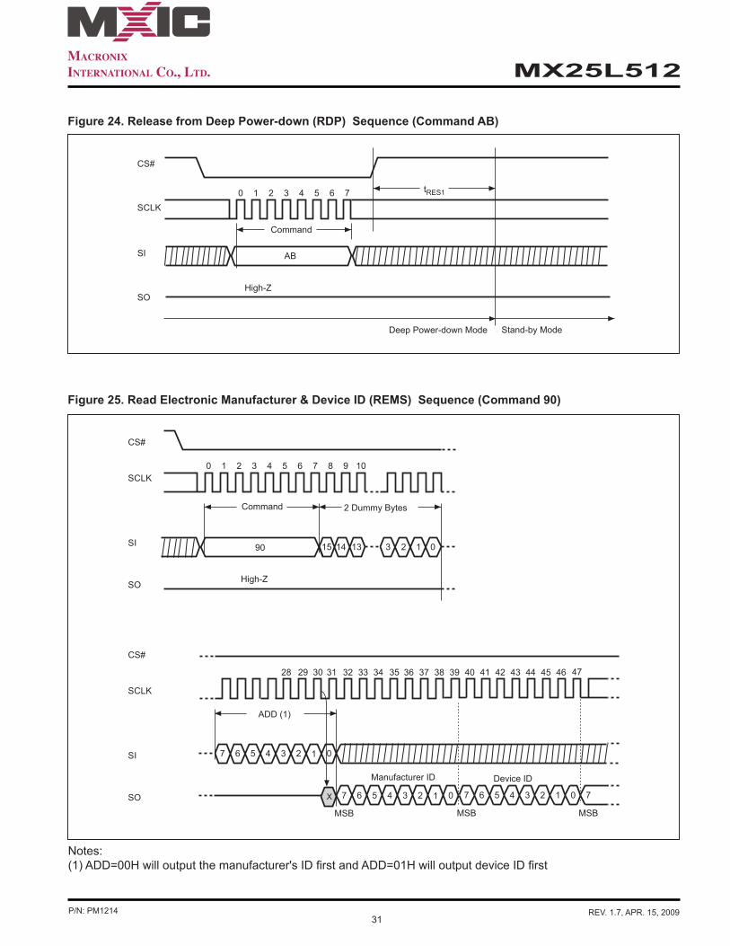
(13) Release from Deep Power-down (RDP), Read Electronic Signature (RES)
The Release from Deep Power-down (RDP) instruction is terminated by driving Chip Select (CS#) High. When Chip Select (CS#) is driven High, the device is put in the Stand-by Power mode. If the device was not previously in the Deep Power-down mode, the transition to the Stand-by Power mode is immediate. If the device was previously in the Deep Power-down mode, though, the transition to the Stand-by Power mode is delayed by tRES2, and Chip Select (CS#) must remain High for at least tRES2(max), as specified in Table 6. Once in the Stand-by Power mode, the device waits to be selected, so that it can receive, decode and execute instructions.
RES instruction is for reading out the old style of 8-bit Electronic Signature, whose values are shown as table of ID Definitions. This is not the same as RDID instruction. It is not recommended to use for new design. For new deisng, please use RDID instruction. Even in Deep power-down mode, the RDP and RES are also allowed to be executed, only except the device is in progress of program/erase/write cycle; there's no effect on the current program/erase/write cycle in progress.
The sequence is shown as Figure 23,24.
The RES instruction is ended by CS# goes high after the ID been read out at least once. The ID outputs repeat-edly if continuously send the additional clock cycles on SCLK while CS# is at low. If the device was not previously in Deep Power-down mode, the device transition to standby mode is immediate. If the device was previously in Deep Power-down mode, there's a delay of tRES2 to transit to standby mode, and CS# must remain to high at least tRES2(max). Once in the standby mode, the device waits to be selected, so it can be receive, decode, and execute instruction.
The RDP instruction is for releasing from Deep Power Down Mode.
at least 1-byte on data on SI→ CS# goes high. (see Figure 18)
The self-timed Page Program Cycle time (tPP) is initiated as soon as Chip Select (CS#) goes high. The Write in Progress (WIP) bit still can be check out during the Page Program cycle is in progress. The WIP sets 1 during the tPP timing, and sets 0 when Page Program Cycle is completed, and the Write Enable Latch (WEL) bit is reset. If the page is protected by BP1, BP0 bits, the Page Program (PP) instruction will not be executed.

16P/N: PM1214 REV. 1.7, APR. 15, 2009
MX25L512
(14) Read Electronic Manufacturer ID & Device ID (REMS)
The REMS instruction is an alternative to the Release from Power-down/Device ID instruction that provides both the JEDEC assigned manufacturer ID and the specific device ID.
The REMS instruction is very similar to the Release from Power-down/Device ID instruction. The instruction is initi-ated by driving the CS# pin low and shift the instruction code "90h" followed by two dummy bytes and one bytes address (A7~A0). After which, the Manufacturer ID for MXIC (C2h) and the Device ID are shifted out on the falling edge of SCLK with most significant bit (MSB) first as shown in figure 25. The Device ID values are listed in Table of ID Definitions on page 16. If the one-byte address is initially set to 01h, then the device ID will be read first and then followed by the Manufacturer ID. The Manufacturer and Device IDs can be read continuously, alternating from one to the other. The instruction is completed by driving CS# high.
Table of ID Definitions:
RDID Command manufacturer ID memory type memory densityC2 20 10
RES Command electronic ID05
REMS Command manufacturer ID device IDC2 05

17P/N: PM1214 REV. 1.7, APR. 15, 2009
MX25L512
POWER-ON STATE
The device is at below states when power-up: - Standby mode ( please note it is not deep power-down mode) - Write Enable Latch (WEL) bit is reset
The device must not be selected during power-up and power-down stage unless the VCC achieves below correct level: - VCC minimum at power-up stage and then after a delay of tVSL - GND at power-downPlease note that a pull-up resistor on CS# may ensure a safe and proper power-up/down level.
An internal power-on reset (POR) circuit may protect the device from data corruption and inadvertent data change during power up state.
For further protection on the device, if the VCC does not reach the VCC minimum level, the correct operation is not guaranteed. The read, write, erase, and program command should be sent after the below time delay: - tVSL after VCC reached VCC minimum levelThe device can accept read command after VCC reached VCC minimum and a time delay of tVSL.Please refer to the figure of "power-up timing".
Note: - To stabilize the VCC level, the VCC rail decoupled by a suitable capacitor close to package pins is recommend-
ed.(generally around 0.1uF)
18P/N: PM1214 REV. 1.7, APR. 15, 2009
MX25L512
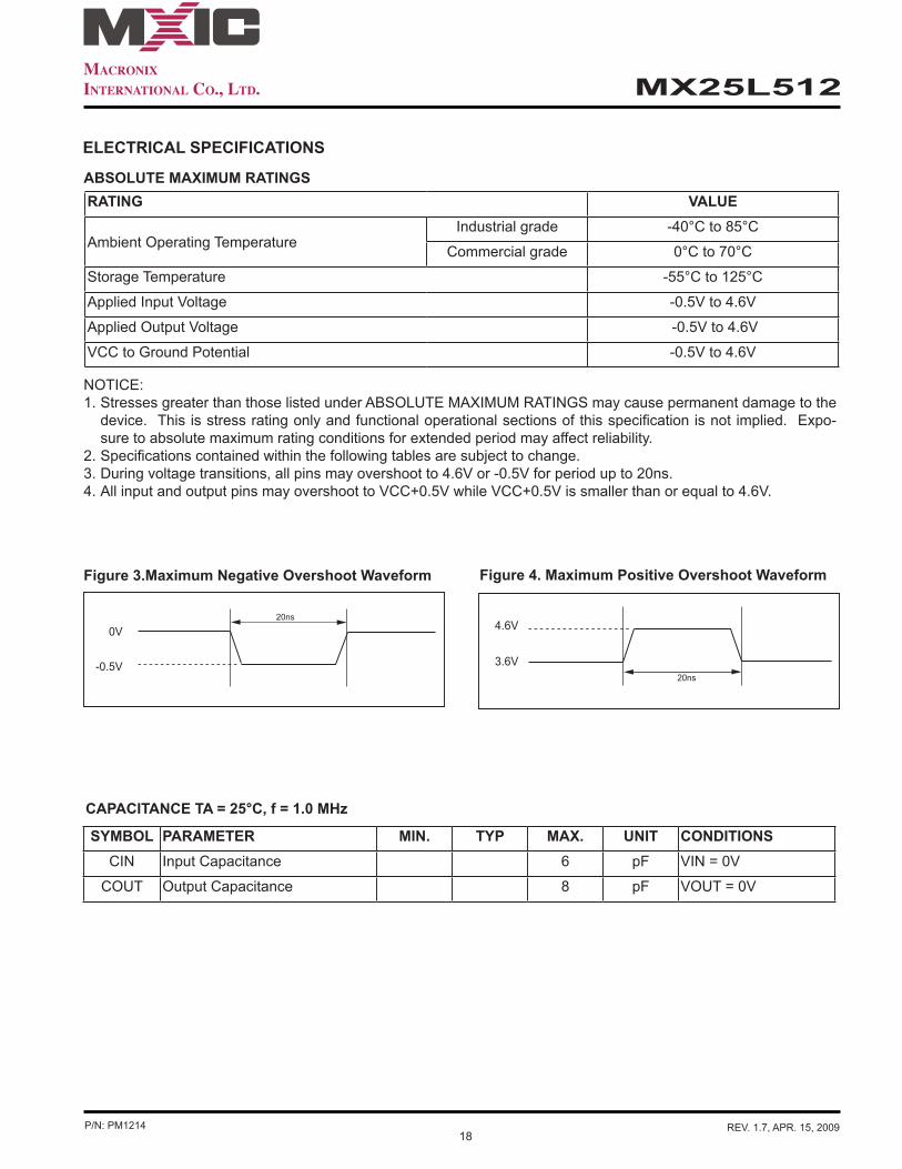
NOTICE:1. Stresses greater than those listed under ABSOLUTE MAXIMUM RATINGS may cause permanent damage to the
device. This is stress rating only and functional operational sections of this specification is not implied. Expo-sure to absolute maximum rating conditions for extended period may affect reliability.
2. Specifications contained within the following tables are subject to change.3. During voltage transitions, all pins may overshoot to 4.6V or -0.5V for period up to 20ns.4. All input and output pins may overshoot to VCC+0.5V while VCC+0.5V is smaller than or equal to 4.6V.
ABSOLUTE MAXIMUM RATINGS
ELECTRICAL SPECIFICATIONS
CAPACITANCE TA = 25°C, f = 1.0 MHz
Figure 3.Maximum Negative Overshoot Waveform Figure 4. Maximum Positive Overshoot Waveform
RATING VALUE
Ambient Operating TemperatureIndustrial grade -40°C to 85°C
Commercial grade 0°C to 70°C
Storage Temperature -55°C to 125°C
Applied Input Voltage -0.5V to 4.6V
Applied Output Voltage -0.5V to 4.6V
VCC to Ground Potential -0.5V to 4.6V
SYMBOL PARAMETER MIN. TYP MAX. UNIT CONDITIONSCIN Input Capacitance 6 pF VIN = 0V
COUT Output Capacitance 8 pF VOUT = 0V
0V
-0.5V
20ns4.6V
3.6V20ns

19P/N: PM1214 REV. 1.7, APR. 15, 2009
MX25L512
Figure 5. INPUT TEST WAVEFORMS AND MEASUREMENT LEVEL
ACMeasurement
Level
Input timing referance level Output timing referance level
0.8VCC0.7VCC
0.3VCC0.5VCC
0.2VCC
Note: Input pulse rise and fall time are <5ns
Figure 6. OUTPUT LOADING
DEVICE UNDER TEST
DIODES=IN3064OR EQUIVALENT
CL6.2K ohm
2.7K ohm+3.3V
CL=30pF Including jig capacitance
(CL=15pF Including jig capacitance for 70MHz)

20P/N: PM1214 REV. 1.7, APR. 15, 2009
MX25L512
SYMBOL PARAMETER NOTES MIN. TYP. MAX. UNITS TEST CONDITIONS
ILI Input Load Current 1 ± 2 uA VCC = VCC MaxVIN = VCC or GND
ILO Output Leakage Current 1 ± 2 uA VCC = VCC MaxVIN = VCC or GND
ISB1 VCC Standby Current 1 10 uA VIN = VCC or GNDCS#=VCC
ISB2 Deep Power-down Current 1 5 uA VIN = VCC or GND
CS#=VCC
ICC1 VCC Read 1
12 mAf=85MHz SCLK=0.1VCC/0.9VCC, SO=Open
8 mAf=66MHzSCLK=0.1VCC/0.9VCC, SO=Open
4 mAf=33MHzSCLK=0.1VCC/0.9VCC, SO=Open
ICC2 VCC Program Current (PP) 1 15 mA Program in Progress
CS#=VCC
ICC3VCC Write Status Register (WRSR) Current
15 mAProgram status register in progressCS#=VCC
ICC4 VCC Sector Erase Current (SE) 1 15 mA Erase in Progress
CS#=VCC
ICC5 VCC Chip Erase Current (CE) 1 15 mA Erase in Progress
CS#=VCCVIL Input Low Voltage -0.5 0.3VCC VVIH Input High Voltage 0.7VCC VCC+0.4 VVOL Output Low Voltage 0.4 V IOL = 1.6mAVOH Output High Voltage VCC-0.2 V IOH = -100uA
Table 5. DC CHARACTERISTICS (Temperature = -40°C to 85°C for Industrial grade, Temperature = 0°C to 70°C for Commercial grade, VCC = 2.7V ~ 3.6V)
Notes :1. Typical values at VCC = 3.3V, T = 25°C. These currents are valid for all product versions (package and speeds).2. Typical value is calculated by simulation.
21P/N: PM1214 REV. 1.7, APR. 15, 2009
MX25L512
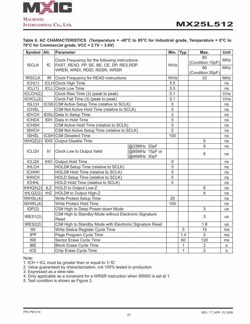
Symbol Alt. Parameter Min. Typ. Max. Unit
fSCLK fCClock Frequency for the following instructions:FAST_READ, PP, SE, BE, CE, DP, RES,RDPWREN, WRDI, RDID, RDSR, WRSR
1KHz
85(Condition:15pF) MHz
66(Condition:30pF)
MHz
fRSCLK fR Clock Frequency for READ instructions 1KHz 33 MHztCH(1) tCLH Clock High Time 5.5 nstCL(1) tCLL Clock Low Time 5.5 ns
tCLCH(2) Clock Rise Time (3) (peak to peak) 0.1 V/nstCHCL(2) Clock Fall Time (3) (peak to peak) 0.1 V/ns
tSLCH tCSS CS# Active Setup Time (relative to SCLK) 5 nstCHSL CS# Not Active Hold Time (relative to SCLK) 5 nstDVCH tDSU Data In Setup Time 2 nstCHDX tDH Data In Hold Time 5 nstCHSH CS# Active Hold Time (relative to SCLK) 5 nstSHCH CS# Not Active Setup Time (relative to SCLK) 5 nstSHSL tCSH CS# Deselect Time 100 ns
tSHQZ(2) tDIS Output Disable Time 6 ns
tCLQV tV Clock Low to Output Valid @33MHz 30pF 8 ns@85MHz 15pF or @66MHz 30pF 6 ns
tCLQX tHO Output Hold Time 0 nstHLCH HOLD# Setup Time (relative to SCLK) 5 nstCHHH HOLD# Hold Time (relative to SCLK) 5 nstHHCH HOLD Setup Time (relative to SCLK) 5 nstCHHL HOLD Hold Time (relative to SCLK) 5 ns
tHHQX(2) tLZ HOLD to Output Low-Z 6 nstHLQZ(2) tHZ HOLD# to Output High-Z 6 nstWHSL(4) Write Protect Setup Time 20 nstSHWL(4) Write Protect Hold Time 100 ns
tDP(2) CS# High to Deep Power-down Mode 3 us
tRES1(2) CS# High to Standby Mode without Electronic Signature Read 3 us
tRES2(2) CS# High to Standby Mode with Electronic Signature Read 1.8 ustW Write Status Register Cycle Time 5 15 mstPP Page Program Cycle Time 1.4 5 mstSE Sector Erase Cycle Time 60 120 mstBE Block Erase Cycle Time 1 2 stCE Chip Erase Cycle Time 1 2 s
Note: 1. tCH + tCL must be greater than or equal to 1/ fC 2. Value guaranteed by characterization, not 100% tested in production.3. Expressed as a slew-rate.4. Only applicable as a constraint for a WRSR instruction when SRWD is set at 1.5. Test condition is shown as Figure 3.
Table 6. AC CHARACTERISTICS (Temperature = -40°C to 85°C for Industrial grade, Temperature = 0°C to 70°C for Commercial grade, VCC = 2.7V ~ 3.6V)

22P/N: PM1214 REV. 1.7, APR. 15, 2009
MX25L512
INITIAL DELIVERY STATE
The device is delivered with the memory array erased: all bits are set to 1 (each byte contains FFh). The Status Register contains 00h (all Status Register bits are 0).
Table 7. Power-Up Timing
Note: 1. The parameter is characterized only.
Symbol Parameter Min. Max. UnittVSL(1) VCC(min) to CS# low 10 us

23P/N: PM1214 REV. 1.7, APR. 15, 2009
MX25L512
Figure 7. Serial Input Timing
Figure 8. Output Timing
LSB
ADDR.LSB IN
tSHQZ
tCH
tCL
tQLQHtQHQL
tCLQX
tCLQVtCLQV
SCLK
SO
CS#
SI
SCLK
SI
CS#
MSB
SO
tDVCH
High-Z
LSB
tSLCH
tCHDX
tCHCL
tCLCH
tSHCH
tSHSL
tCHSHtCHSL

24P/N: PM1214 REV. 1.7, APR. 15, 2009
MX25L512
Figure 9. Hold Timing
* SI is "don't care" during HOLD operation.
Figure 10. WP# Disable Setup and Hold Timing during WRSR when SRWD=1
tCHHL
tHLCH
tHHCH
tCHHH
tHHQXtHLQZ
SCLK
SO
CS#
HOLD#
High-Z
01
0 1 2 3 4 5 6 7 8 9 10 11 12 13 14 15
tWHSLtSHWL
SCLK
SI
CS#
WP#
SO
25P/N: PM1214 REV. 1.7, APR. 15, 2009
MX25L512
Figure 11. Write Enable (WREN) Sequence (Command 06)
Figure 12. Write Disable (WRDI) Sequence (Command 04)
Figure 13. Read Identification (RDID) Sequence (Command 9F)
21 3 4 5 6 7
High-Z
0
06
Command
SCLK
SI
CS#
SO
21 3 4 5 6 7
High-Z
0
04
Command
SCLK
SI
CS#
SO
21 3 4 5 6 7 8 9 10 11 12 13 14 15
Command
0
Manufacturer IdentificationHigh-Z
MSB
15 14 13 3 2 1 0
Device Identification
MSB
7 6 5 3 2 1 0
16 17 18 28 29 30 31
SCLK
SI
CS#
SO
9F

26P/N: PM1214 REV. 1.7, APR. 15, 2009
MX25L512
Figure 14. Read Status Register (RDSR) Sequence (Command 05)
Figure 15. Write Status Register (WRSR) Sequence (Command 01)
Figure 16. Read Data Bytes (READ) Sequence (Command 03)
21 3 4 5 6 7 8 9 10 11 12 13 14 15
command
0
7 6 5 4 3 2 1 0
Status Register OutHigh-Z
MSB
7 6 5 4 3 2 1 0
Status Register Out
MSB
7
SCLK
SI
CS#
SO
05
21 3 4 5 6 7 8 9 10 11 12 13 14 15
StatusRegister In
0
7 6 5 4 3 2 01
MSB
SCLK
SI
CS#
SO
01
High-Z
command
SCLK
SI
CS#
SO
23
21 3 4 5 6 7 8 9 10 28 29 30 31 32 33 34 35
22 21 3 2 1 0
36 37 38
7 6 5 4 3 1 70
Data Out 1
24-Bit Address
0
MSB
MSB
2
39
Data Out 2
03
High-Z
command

27P/N: PM1214 REV. 1.7, APR. 15, 2009
MX25L512
Figure 17. Read at Higher Speed (FAST_READ) Sequence (Command 0B)
23
21 3 4 5 6 7 8 9 10 28 29 30 31
22 21 3 2 1 0
High-Z
24 BIT ADDRESS
0
32 33 34 36 37 38 39 40 41 42 43 44 45 46
7 6 5 4 3 2 01
DATA OUT 1
Dummy Byte
MSB
7 6 5 4 3 2 1 0
DATA OUT 2
MSB MSB
7
47
7 6 5 4 3 2 01
35
SCLK
SI
CS#
SO
SCLK
SI
CS#
SO
0B
Command

28P/N: PM1214 REV. 1.7, APR. 15, 2009
MX25L512
Figure 18. Page Program (PP) Sequence (Command 02)
4241 43 44 45 46 47 48 49 50 52 53 54 5540
23
21 3 4 5 6 7 8 9 10 28 29 30 31 32 33 34 35
22 21 3 2 1 0
36 37 38
24-Bit Address
0
7 6 5 4 3 2 01
Data Byte 1
39
51
7 6 5 4 3 2 01
Data Byte 2
7 6 5 4 3 2 01
Data Byte 3 Data Byte 256
2079
2078
2077
2076
2075
2074
2073
7 6 5 4 3 2 01
2072
MSB MSB
MSB MSB MSB
SCLK
CS#
SI
SCLK
CS#
SI
02
Command

29P/N: PM1214 REV. 1.7, APR. 15, 2009
MX25L512
Figure 19. Sector Erase (SE) Sequence (Command 20)
Note: SE command is 20(hex).
Figure 20. Block Erase (BE) Sequence (Command 52 or D8)
Note: BE command is 52 or D8(hex).
24 Bit Address
21 3 4 5 6 7 8 9 29 30 310
7 6 2 1 0
MSB
SCLK
CS#
SI 20
Command
24 Bit Address
21 3 4 5 6 7 8 9 29 30 310
23 22 2 01
MSB
SCLK
CS#
SI 52 or D8
Command

30P/N: PM1214 REV. 1.7, APR. 15, 2009
MX25L512
Figure 21. Chip Erase (CE) Sequence (Command 60 or C7)
Figure 22. Deep Power-down (DP) Sequence (Command B9)
Figure 23. Release from Deep Power-down and Read Electronic Signature (RES) Sequence (Command AB)
Note: CE command is 60(hex) or C7(hex).
21 3 4 5 6 70
60 or C7
SCLK
SI
CS#
Command
21 3 4 5 6 70 tDP
Deep Power-down ModeStand-by Mode
SCLK
CS#
SI B9
Command
23
21 3 4 5 6 7 8 9 10 28 29 30 31 32 33 34 35
22 21 3 2 1 0
36 37 38
7 6 5 4 3 2 01High-Z
Electronic Signature Out
3 Dummy Bytes
0
MSB
Stand-by ModeDeep Power-down Mode
MSB
tRES2
SCLK
CS#
SI
SO
AB
Command
31P/N: PM1214 REV. 1.7, APR. 15, 2009
MX25L512
Figure 24. Release from Deep Power-down (RDP) Sequence (Command AB)
Figure 25. Read Electronic Manufacturer & Device ID (REMS) Sequence (Command 90)
Notes:(1) ADD=00H will output the manufacturer's ID first and ADD=01H will output device ID first
21 3 4 5 6 70 tRES1
Stand-by ModeDeep Power-down Mode
High-Z
SCLK
CS#
SI
SO
AB
Command
15 14 13 3 2 1 0
21 3 4 5 6 7 8 9 10
2 Dummy Bytes
0
32 33 34 36 37 38 39 40 41 42 43 44 45 46
7 6 5 4 3 2 01
Manufacturer ID
ADD (1)
MSB
7 6 5 4 3 2 1 0
Device ID
MSB MSB
7
47
7 6 5 4 3 2 01
3531302928
SCLK
SI
CS#
SO
SCLK
SI
CS#
SO X
90
High-Z
Command

32P/N: PM1214 REV. 1.7, APR. 15, 2009
MX25L512
Figure 26. Power-up Timing
VCC
VCC(min)
Chip Selection is Not Allowed
tVSL
time
Device is fullyaccessible
VCC(max)

33P/N: PM1214 REV. 1.7, APR. 15, 2009
MX25L512
RECOMMENDED OPERATING CONDITIONS
At Device Power-Up
AC timing illustrated in Figure A is recommended for the supply voltages and the control signals at device power-up. If the timing in the figure is ignored, the device may not operate correctly.
Figure A. AC Timing at Device Power-Up
Notes :1. Sampled, not 100% tested.2. For AC spec tCHSL, tSLCH, tDVCH, tCHDX, tSHSL, tCHSH, tSHCH, tCHCL, tCLCH in the figure, please refer to
"AC CHARACTERISTICS" table.
Symbol Parameter Notes Min. Max. UnittVR VCC Rise Time 1 0.5 500000 us/V
SCLK
SI
CS#
VCC
MSB IN
SO
tDVCH
High Impedance
LSB IN
tSLCH
tCHDX
tCHCL
tCLCH
tSHCH
tSHSL
tCHSHtCHSL
tVR
VCC(min)
GND
34P/N: PM1214 REV. 1.7, APR. 15, 2009
MX25L512
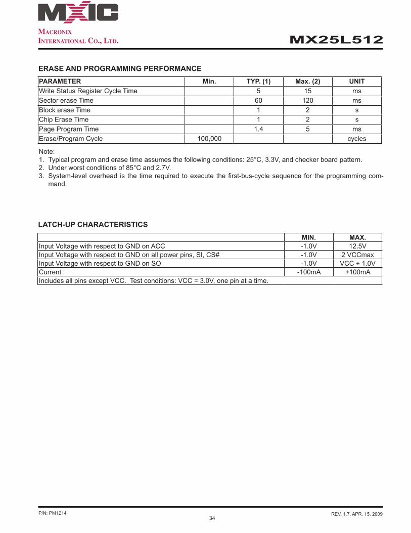
ERASE AND PROGRAMMING PERFORMANCEPARAMETER Min. TYP. (1) Max. (2) UNITWrite Status Register Cycle Time 5 15 msSector erase Time 60 120 msBlock erase Time 1 2 sChip Erase Time 1 2 sPage Program Time 1.4 5 msErase/Program Cycle 100,000 cycles
Note: 1. Typical program and erase time assumes the following conditions: 25°C, 3.3V, and checker board pattern.2. Under worst conditions of 85°C and 2.7V.3. System-level overhead is the time required to execute the first-bus-cycle sequence for the programming com-
mand.
MIN. MAX.
Input Voltage with respect to GND on ACC -1.0V 12.5VInput Voltage with respect to GND on all power pins, SI, CS# -1.0V 2 VCCmaxInput Voltage with respect to GND on SO -1.0V VCC + 1.0VCurrent -100mA +100mAIncludes all pins except VCC. Test conditions: VCC = 3.0V, one pin at a time.
LATCH-UP CHARACTERISTICS
35P/N: PM1214 REV. 1.7, APR. 15, 2009
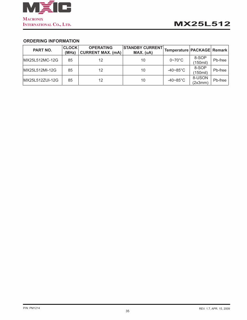
MX25L512
PART NO. CLOCK (MHz)
OPERATING CURRENT MAX. (mA)
STANDBY CURRENT MAX. (uA) Temperature PACKAGE Remark
MX25L512MC-12G 85 12 10 0~70°C 8-SOP (150mil) Pb-free
MX25L512MI-12G 85 12 10 -40~85°C 8-SOP (150mil) Pb-free
MX25L512ZUI-12G 85 12 10 -40~85°C 8-USON (2x3mm) Pb-free
ORDERING INFORMATION

36P/N: PM1214 REV. 1.7, APR. 15, 2009
MX25L512
PART NAME DESCRIPTION
MX 25 L 12 M I GOPTION:G: Pb-freeblank: normal
SPEED:12: 85MHz
TEMPERATURE RANGE:I: Industrial (-40℃ to 85℃)C: Commercial (0℃ to 70℃)
PACKAGE:M: 150mil 8-SOPZU: 2x3mm 8-USON
DENSITY & MODE:512: 512Kb
TYPE:L: 3V
DEVICE:25: Serial Flash
512

37P/N: PM1214 REV. 1.7, APR. 15, 2009
MX25L512
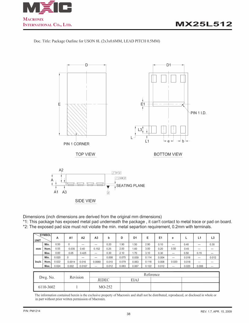
PACKAGE INFORMATION
38P/N: PM1214 REV. 1.7, APR. 15, 2009
MX25L512
39P/N: PM1214 REV. 1.7, APR. 15, 2009
MX25L512
REVISION HISTORY
Revision No. Description Page Date1.0 1. Modified read current:6mA@85MHz/4mA@66MHz/2mA@33MHz P1,18,33 OCT/03/2005 → 12mA@85MHz/8mA@66MHz/4mA@33MHz 2. Modified tSE:90ms(typ)/270ms(max)→60ms(typ)/120ms(max) ; P1,19,32 tBE:3s(max)→2s(max); tCE:3s(max)→2s(max) 3. Added description about Pb-free device is RoHS compliant P1 4. Removed "Advanced Information" title P1 5. Added C-grade part number P331.1 1. Format change All JUN/08/2006 2. Supplemented the footnote for tW of protect/unprotect bits P91.2 1. Added statement P38 NOV/06/20061.3 1. Defined min. clock frequency of fSCLK & fRSCLK as 1KHz P20 NOV/30/20061.4 1. Removed 8-land SON package and order information P2,3,34,35 MAR/24/20081.5 1. Removed wrong Block Protect bit: BP2 P5,11 AUG/12/2008 2. Removed non Pb-free EPN P34,351.6 1. Modified Figure 13, 14, 16, 17, 23 (waveform) P24,25,26,29 FEB/17/2009 2. Added 8-USON package P3,34,37 3. Removed "Low Vcc write inhibit" function P1,5,16,21,31 4. Changed tCH/tCL spec from 7/7(ns) to 5.5/5.5(ns) P201.7 1. Announced "not recommended for new designs" wording P1,2 APR/15/2009

MX25L512
40
MACRONIX INTERNATIONAL CO., LTD.
Macronix Offices : Taiwan Headquarters, FAB2 Macronix, International Co., Ltd. 16, Li-Hsin Road, Science Park, Hsinchu, Taiwan, R.O.C. Tel: +886-3-5786688 Fax: +886-3-5632888
Taipei Office Macronix, International Co., Ltd. 19F, 4, Min-Chuan E. Road, Sec. 3, Taipei, Taiwan, R.O.C. Tel: +886-2-2509-3300 Fax: +886-2-2509-2200
Macronix Offices : China Macronix (Hong Kong) Co., Limited. 702-703, 7/F, Building 9, Hong Kong Science Park, 5 Science Park West Avenue, Sha Tin, N.T. Tel: +86-852-2607-4289 Fax: +86-852-2607-4229
Macronix (Hong Kong) Co., Limited, SuZhou Office No.5, XingHai Rd, SuZhou Industrial Park, SuZhou China 215021 Tel: +86-512-62580888 Ext: 3300 Fax: +86-512-62586799
Macronix (Hong Kong) Co., Limited, Shenzhen Office Room 1401 & 1404, Blcok A, TianAN Hi-Tech PLAZA Tower, Che Gong Miao, FutianDistrict, Shenzhen PRC 518040 Tel: +86-755-83433579 Fax: +86-755-83438078
http : //www.macronix.com
MACRONIX INTERNATIONAL CO., LTD. reserves the right to change product and specifications without notice.
Macronix Offices : Japan Macronix Asia Limited. NKF Bldg. 5F, 1-2 Higashida-cho, Kawasaki-ku Kawasaki-shi, Kanagawa Pref. 210-0005, Japan Tel: +81-44-246-9100 Fax: +81-44-246-9105
Macronix Offices : Korea Macronix Asia Limited. #906, 9F, Kangnam Bldg., 1321-4, Seocho-Dong, Seocho-Ku, 135-070, Seoul, Korea Tel: +82-02-588-6887 Fax: +82-02-588-6828
Macronix Offices : Singapore Macronix Pte. Ltd. 1 Marine Parade Central, #11-03 Parkway Centre, Singapore 449408 Tel: +65-6346-5505 Fax: +65-6348-8096
Macronix Offices : Europe Macronix Europe N.V. Koningin Astridlaan 59, Bus 1 1780 Wemmel Belgium Tel: +32-2-456-8020 Fax: +32-2-456-8021
Macronix Offices : USA Macronix America, Inc. 680 North McCarthy Blvd. Milpitas, CA 95035, U.S.A. Tel: +1-408-262-8887 Fax: +1-408-262-8810
Macronix's products are not designed, manufactured, or intended for use for any high risk applications in which the failure of a single component could cause death, personal injury, severe physical damage, or other substan-tial harm to persons or property, such as life-support systems, high temperature automotive, medical, aircraft and military application. Macronix and its suppliers will not be liable to you and/or any third party for any claims, injuries or damages that may be incurred due to use of Macronix's products in the prohibited applications.
Copyright© Macronix International Co. Ltd. 2005~2009. All Rights Reserved. Macronix, MXIC, MXIC Logo, MX Logo, are trademarks or registered trademarks of Macronix International Co., Ltd.. The names and brands of other companies are for identification purposes only and may be claimed as the property of the respective companies.